

Page 1
TROUBLE SHOOTING GUIDE
MODEL
.............. ......... ....................
DEST. CHASSIS NO. MODEL DEST. CHASSIS NO.
PFM-500A1WU US/CND
PFM-500A1WE AEP
.............. ......... ....................
MB-514
RM-921
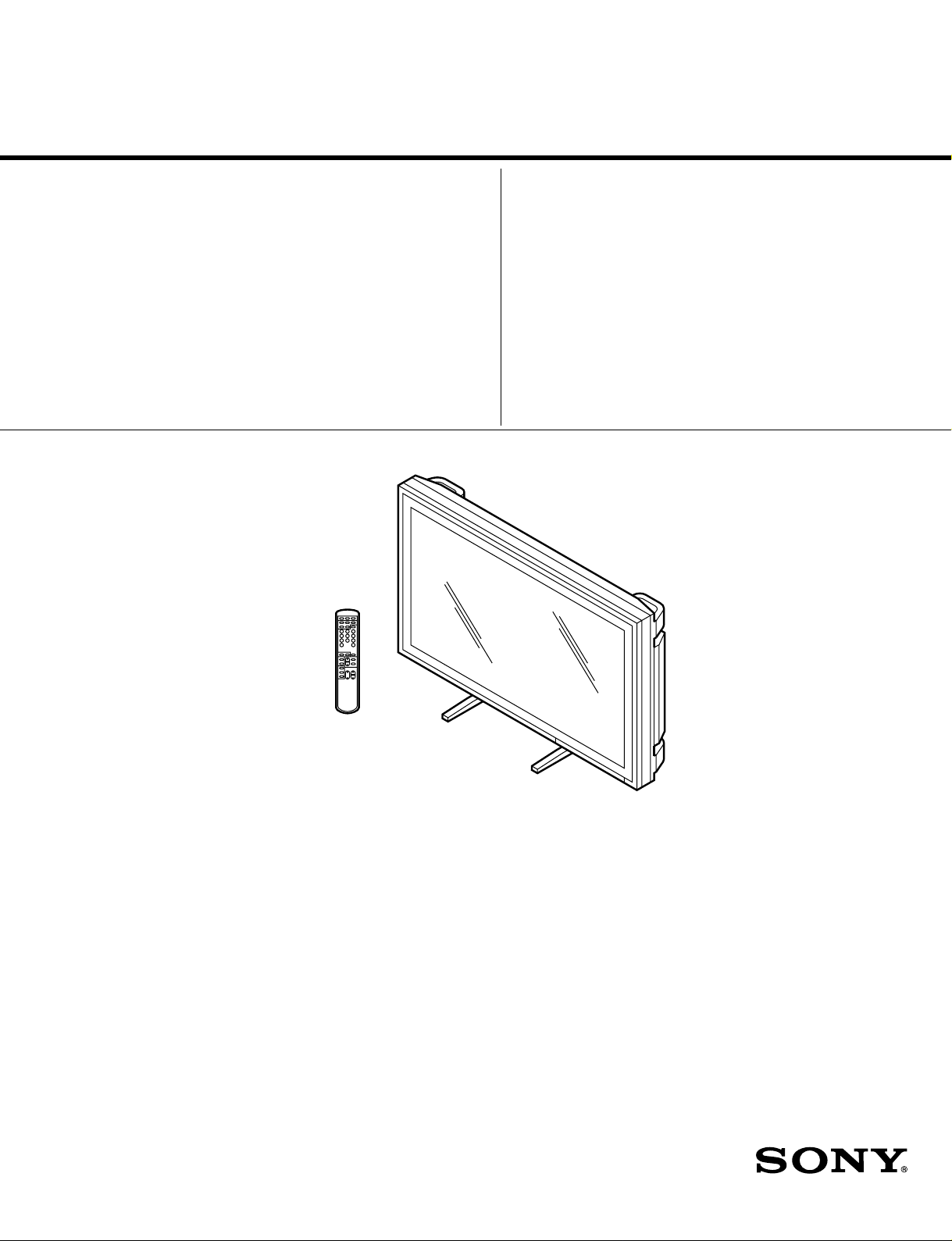
PFM-500A1WU/WE Flat Panel Monitor
MB-514 Mounting Bracket
RM-921 Remote Commander
FLAT PANEL MONITOR
Page 2

! WARNING
This manual is intended for qualified service personnel only.
To reduce the risk of electric shock, fire or injury, do not perform any servicing other than that
contained in the operating instructions unless you are qualified to do so. Refer all servicing to
qualified service personnel.
! WARNUNG
Die Anleitung ist nur für qualifiziertes Fachpersonal bestimmt.
Alle Wartungsarbeiten dürfen nur von qualifiziertem Fachpersonal ausgeführt werden. Um die
Gefahr eines elektrischen Schlages, Feuergefahr und Verletzungen zu vermeiden, sind bei
Wartungsarbeiten strikt die Angaben in der Anleitung zu befolgen. Andere als die angegeben
Wartungsarbeiten dürfen nur von Personen ausgeführt werden, die eine spezielle Befähigung
dazu besitzen.
! AVERTISSEMENT
Ce manual est destiné uniquement aux personnes compétentes en charge de l’entretien. Afin
de réduire les risques de décharge électrique, d’incendie ou de blessure n’effectuer que les
réparations indiquées dans le mode d’emploi à moins d’être qualifié pour en effectuer d’autres.
Pour toute réparation faire appel à une personne compétente uniquement.
PFM-500A1WU/500A1WE
Page 3

Table of Contents
1. Introduction
1-1. PDP Unit (FPF42C10660UD) Analysis Manual ........................................1-1
1-2. Test Equipment ...........................................................................................1-2
1-3. Burn-in Device ............................................................................................1-3
1-4. Measuring Device .......................................................................................1-3
1-5. Parts List and Their Outlined Description of the PDP Unit........................1-4
2. Repair Flow........................................................................................... 2-1
3. Data
3-1. Check Point (X-SUS) .................................................................................. 3-1
3-2. Check Point (Y-COM) ................................................................................3-2
3-3. Check Point (DC/DC) ................................................................................. 3-3
3-4. Check Point of Voltage (X-SUS, Y-SUS) ..................................................3-4
3-5. Glossary....................................................................................................... 3-5
3-6. Connection to Test Equipment....................................................................3-6
3-7. Test Equipment ...........................................................................................3-7
3-8. Photo (Burn-in Unit) ................................................................................... 3-8
3-9. Burn-in Unit Instruction Manual.................................................................3-9
3-10. Criteria Table ............................................................................................3-13
3-11. Voltage Setting Procedure.........................................................................3-19
3-12. Display Test Manual ................................................................................. 3-24
3-13. VG-826 Program Display Pattern .............................................................3-28
3-14. Fixed Display Exclusive-key Pattern ........................................................3-30
3-15. Decision Criteria Table ............................................................................. 3-31
3-16. PC Board Replacing Proceduce ................................................................ 3-32
3-17. Each PC Board Installation Screw Position/Connector Position ..............3-33
PFM-500A1WU/500A1WE
1
Page 4

Page 5

1. Introduction
1-1. PDP Unit (FPF42C10660UD) Analysis Manual
This manual explains the failure analysis procedure l for PDP unit and it is applied to analysis by
the test equipment below. To perform failure analysis, see the data, as follows :
. Repair flow
. Check point (X-SUS) ............................ 3-1.
. Check point (Y-COM) .......................... 3-2.
. Check point (DC/DC) ........................... 3-3.
. Voltage check........................................ 3-4.
. Glossary ................................................ 3-5.
. Connection to test equipment ................ 3-6.
. Test equipment....................................... 3-7.
. Photo (Burn-in unit) .............................. 3-8.
. Burn-in unit Instruction Manual ........... 3-9.
. Criteria table.......................................... 3-10.
. Voltage setting procedure ..................... 3-11.
. Display test Manual .............................. 3-12.
. PC board replacing procedure............... 3-16.
Always, allow the self electrical discharge about 30 seconds between shutting down the external power
supply and the operation of replacing each PC board or disconnecting connectors in the repair and
analysis process.
PFM-500A1WU/500A1WE
1-1
Page 6

1-2. Test Equipment (3-6, 7)
Display test is conducted with the facilities listed below and whether the test results can satisfy the criteria
is determined by the display special point standard in the 3-11.
<Facilities used>
1. Video signal generator : Astro design VG-826 (Refer to the 3-12)
2. External keyboard : Astro design RB-614C (Refer to the 3-12)
3. PDP function test switch (APC/DISP ENABLE/HQEN/luminance variable volume)
1 APC (monitoring power consumption/abnormal operation)
ON: NEW.APC mode [Stability hour (about 3 minutes)]
It can monitor the power consumption on the circuit to maintain the rating power.
In addition, it can monitor the X/YSUS operation and shut down the PDP circuit immediately
when any abnormal operation is detected. This prevents further damage to the circuit.
OFF: OLD.APC mode [Stability hour (about 10 seconds)]
In this mode, the internal power supply is activated forcibly to run the electricity
on the circuit, regardless of whether abnormal operation is detected.
Set this mode with care for failure analysis.
The use of APC switch in “OFF” mode may likely cause a secondary failure. Thus, handle this switch
with care. Do not power on the external power supplies at one time.
2 DISP ENABLE (screen display ON/OFF)
ON : Every operation of displaying data is disabled.
OFF : Every operation of displaying data is enabled.
3 HQEN ENABLE (false frame line deletion function)
ON : The difference of each step is lightened in gradation display
OFF : Each step in gradation is displayed as it is and false frame line can be seen.
4 Luminance variable volume (for changing the screen luminance)
Turn the volume to the right to increase the brightness or turn the volume to the left to decrease
the brightness.
4. External power supplies (See the 3-7)
1 Vcc 0 ~ 6 V 10 A
2 Va 0 ~ 110 V 2.0 A
3 Vs 0 ~ 250 V 15 A
* Observe the following sequence, as shown below when using external power supplies:
Power ON : Vcc → Va → Vs
Power OFF : Vs → Va → Vcc
5. Power supply for exclusive use (See the 3-6)
FPF10P-AC100/240 B Rev.B
1-2
PFM-500A1WU/500A1WE
Page 7

1-3. Burn-in Device (3-8) 1
(for the Handling Method, Refer to 3-9.)
1-4. Measuring Device
1 Oscilloscope...................... 1 (equivalent to 100 MHz)
2 Digital Multimeter ............ 1
3 Analog tester ..................... 1
PFM-500A1WU/500A1WE
1-3
Page 8
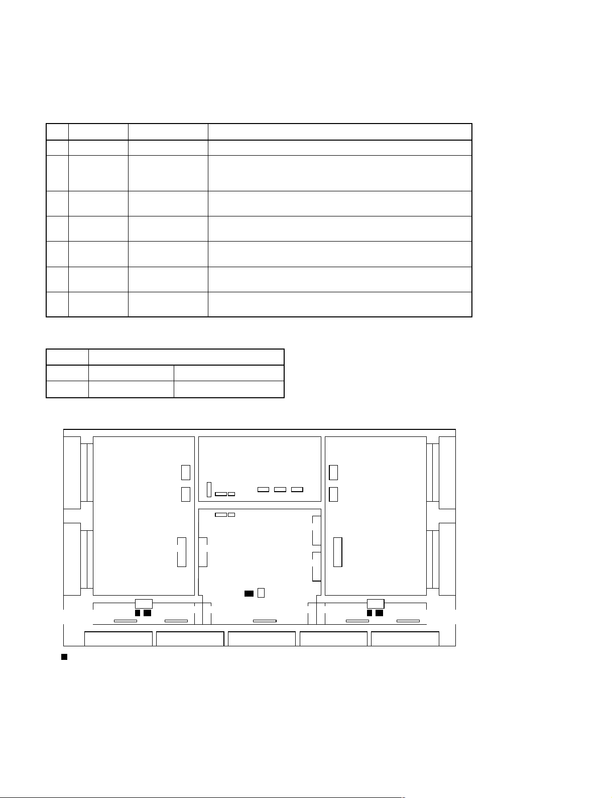
1-5. Parts List and Their Outlined Description of the PDP Unit
<Outlined description of each part>
No NAME Drawing number Basic operation outline
1 Panel FPF10R-UCPANEL Processes and displays data in image processing
2 Logic FPF10R-LOGIC12 Stores and processes data and monitors the power consumption and
PC board X/YSUS operation.
3 XSUS FPF10R-XSUS Controls reservation, deletion, and writing of display data.
PC board
4 YSUS FPF10R-YSUS13 Controls writing and reservation of display data.
PC board
5 RBUS FPF10R-ABUSR Controls output of screen data to ACOM1, 2.
PC board
6 LBUS FPF10R-ABUSL Controls output of screen data to ACOM4, 5.
PC board
7 DC/DC FPF10R-DC/DC Generates the secondary power supplies Ve. Vsc.
PC board Vw. and _Vy by the external power supply.
<EP ROM and YSUS Correspondence table>
Model UD01
ROM 197G 197L
YSUS NA21701-B192 NA21701-B241
Controls output of screen data to ACOM3.
<Mounting diagram each PC board (rear view)>
YCOM UP
CN
YCOM DOWN
CN
LBUS PC board
Fuse mounting position
46
47
CN43
CN44
ACOM5
YSUS PC board
CN18
CN13
CN41
CN42
CN40
CN17
CN12
ACOM4
CN30
CN20CN37
CN37
CN5CN4
CN3
CN18
DC/DC
CN49
CN25CN24CN23
CN2
Logic PC board
1 or 2
CN9
CN16
ACOM3 ACOM2 ACOM1
CN1
CN7
CN50
XSUS PC board
CN48
CN10
CN15
CN11
CN51
CN52
CN14
XBUS UP
CN
53
XBUS DOWN
CN
54
RBUS PC board
1-4
PFM-500A1WU/500A1WE
Page 9
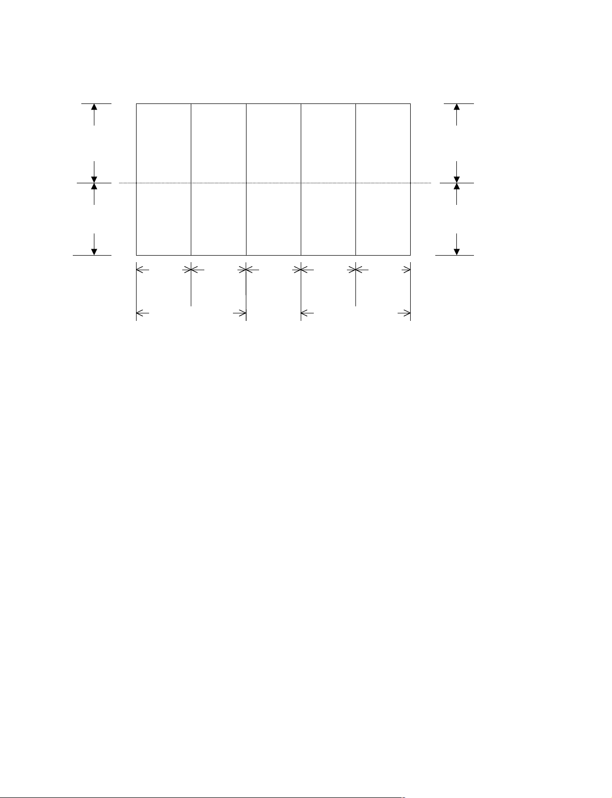
<Control section of each display (front view)>
XBUS UP
Display control
section
XBUS DOWN
Display control
section
1/2 1/2
Panel
1/2
1/5
1/5 1/5 1/5 1/5
ACOM1 ACOM2 ACOM 3 ACOM4 ACOM5
Display control
section
FUSE2 FUSE1
RBUS control section LBUS control section
Display control
section
Display control
section
FUSE201
Logic control
Display control
section
FUSE2
Display control
section
FUSE1
section
1/2
YCOM UP
Display control
section
YCOM DOWN
Display control
section
PFM-500A1WU/500A1WE
1-5
Page 10

Page 11
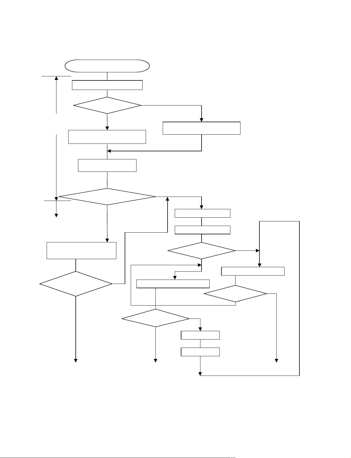
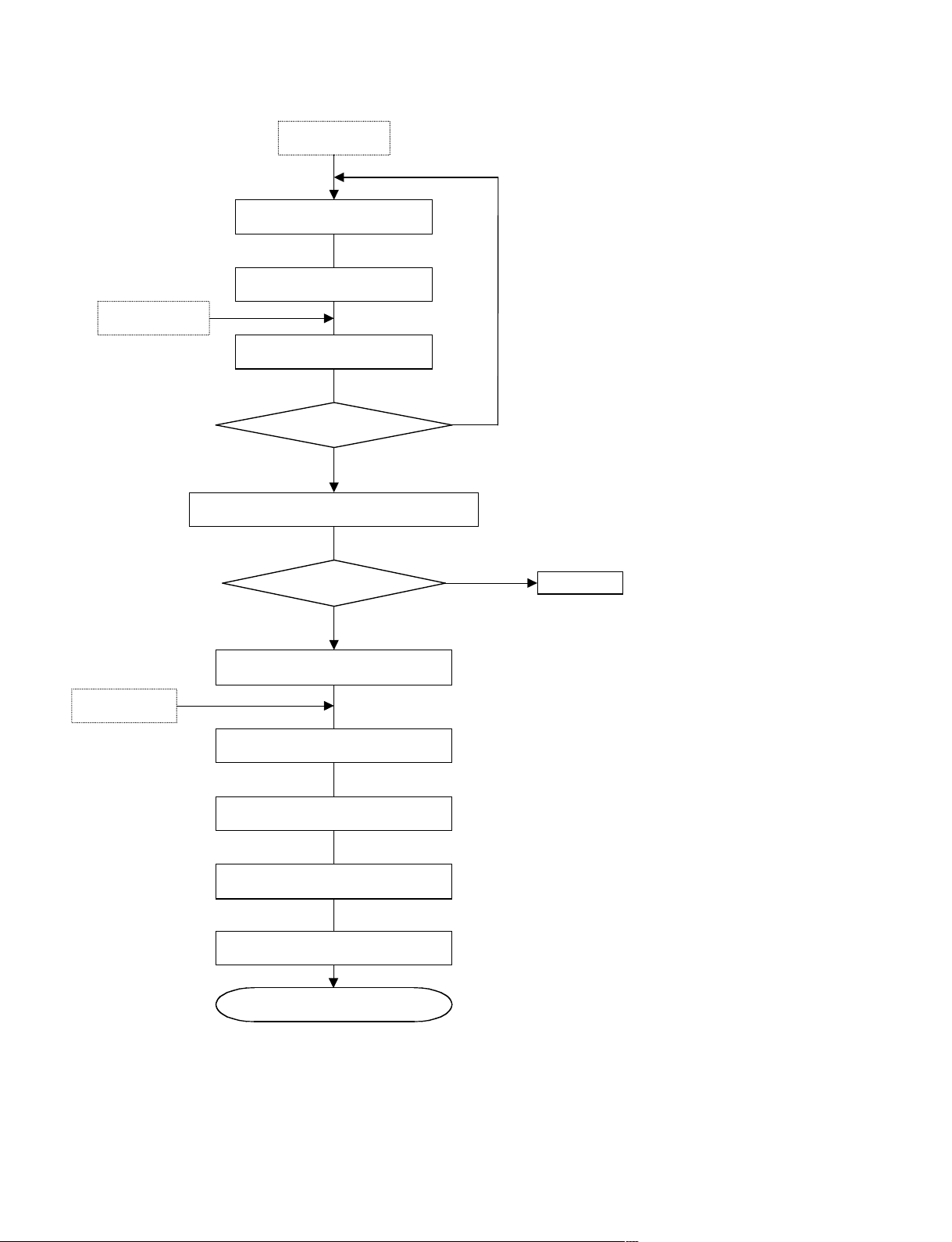
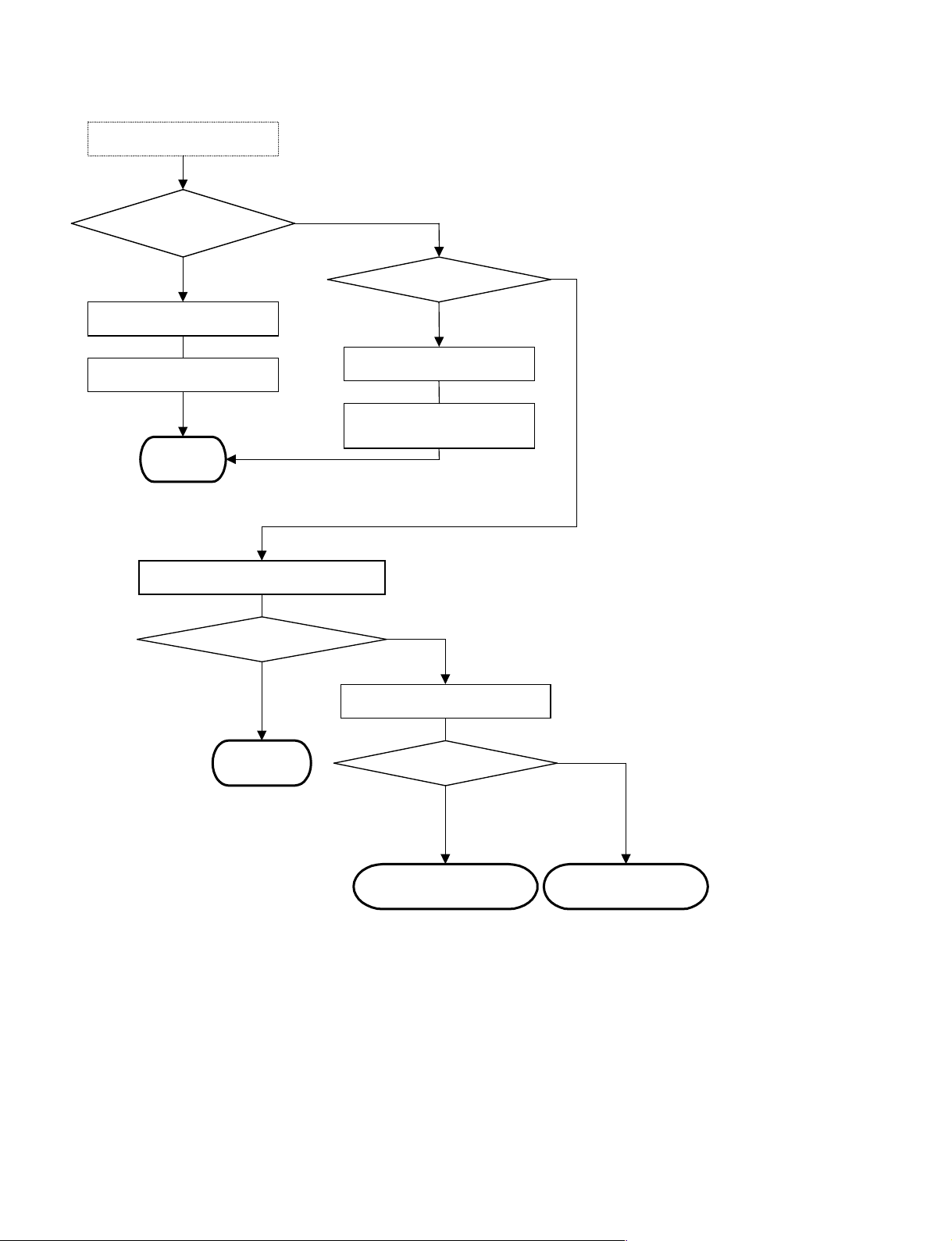
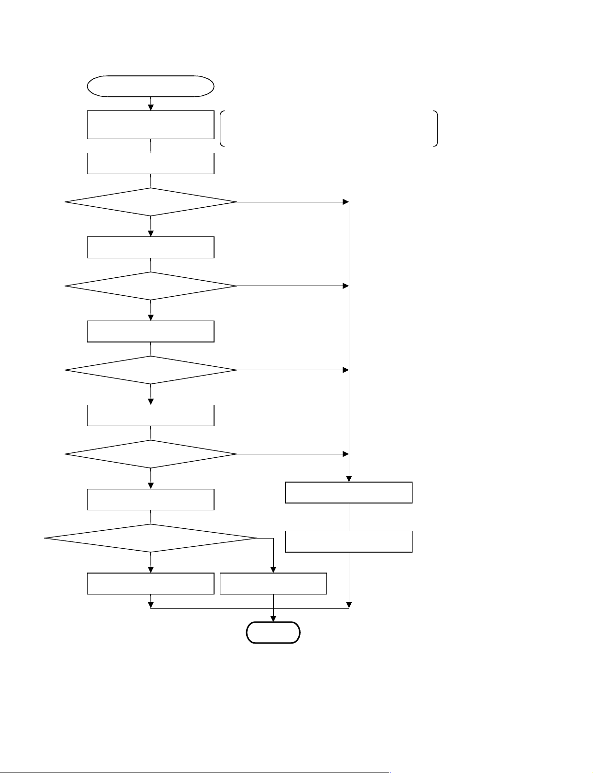
2. Repair Flow
Acceptance of returned unit
Check the contents of a fault
Before repair flow
Check the contents of a fault
according to IRIS CODE table.
Appearance inspection
Appearance defect?
Starts repair flow
Repair the defective position
Repair part describing clearly
Appearance
repair request?
Yes
IRIS CODE
Yes
Yes
No
No
Check the contents of a request
No
Connect to test device
Connect to test device
Fault occurs?
Check the contents of fault request
Yes
No
Non-recurrent analysis mode
Fault occurs?
Yes
No
Go to 6 (P2-2) Go to 1 (P2-2) Go to 3 (P2-2)
PFM-500A1WU/500A1WE
Appearance defect?
Yes
No
Failure analysis
Repair
2-1
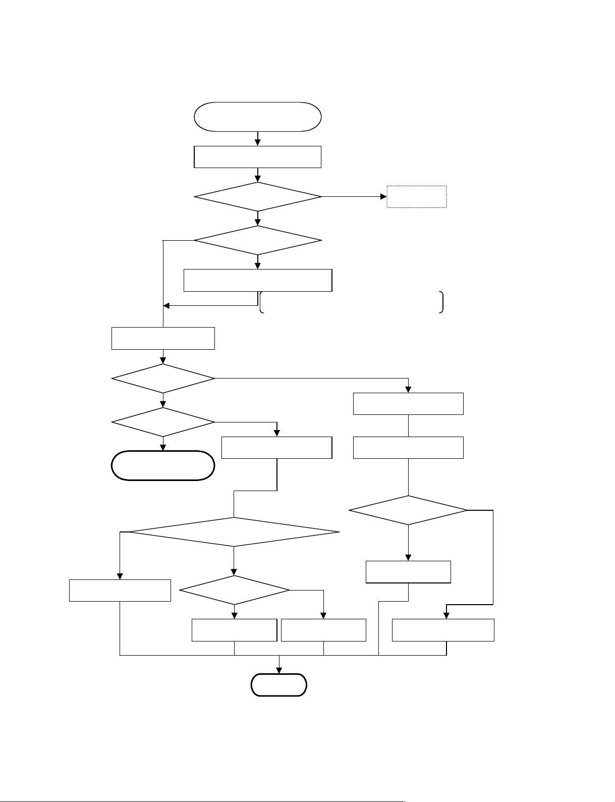
Page 12
From 6 (P2-1)
From 1 (P2-1)
Failure analysis
Repair the defective position
Display test
From 3 (P2-1)
Repair complete?
Yes
Re-install the defective parts (except panel).
Fault recur?
Yes
Change the defective parts again.
Check the CPU/ROM revision No.
Conduct display function test.
No
No
Repair
Go to 4 (P2-1)
2-2
Assurance test (running)
Repair complete
END (Shipping)
PFM-500A1WU/500A1WE
Page 13
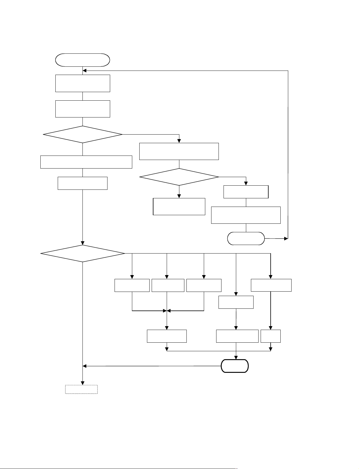
t
START
Test equipment
MAIN-SW ON
Signal generator
SW ON
* A-1 to A-4: See the 3-10 (P3-13)
A-1
Operation OK?
Check the contents of a fault
Appearance check
A-3
Appearance OK?
Yes
Yes
No
No
COM failure
Power supply AC100V measure
(MAIN-SW IN/OUT)
A-2
AC100V OK?
Yes
Fault of Test device
Repair request
Panel failure
Flexible cable
failure
No
MAIN-SW OFF
AC power supply correction
treatment execution
ART
ST
Other appearance
defect
Go to P2-4
PFM-500A1WU/500A1WE
Change panel
Lacking parts
Supply, change Repair
TEST
2-3
Page 14
From P2-3
Protect-cover installation
Fixes to the unit folder
Signal cable is connected with
Logic PC board (CN1)
Special power supply connection
APC function ON Program-key
PUSH “01”
Remote-control SW ON
Analysis A
Fixes to the unit folder
A-4
Screen lighting?
Yes
Evaluation analysis
Go to P2-11
No
Remote-control SW OFF
Separation of Special power supply
External power supply connection
APC function OFF
Program-key PUSH “01”
Go to P2-5
Signal cable is connected with
Logic PC board (CN1)
Analysis B
2-4
PFM-500A1WU/500A1WE
Page 15
From P2-4
Vcc ON
Vcc is gradually raised, and the voltage is set to 5V.
* B-1 to B-!- : See the 3-10 (P3-13)
B-1
Overcurrent?
No
Yes
External power supply OFF
Separation of SUS
Go to P2-7
Va is gradually raised, and the voltage is set to 65V.
No
APC function ON/Vs ON Vs is gradually raised,
and the voltage is set to 180V.
B-6
Overcurrent?
No
Vcc OFF→ON
B-2
Overcurrent?
Yes
Va ON
B-5
Overcurrent?
Yes
External power supply OFF
Go to P2-6
No
No
No
B-3
Vcc or Va checks?
Yes
B-4
Xsus or Ysus separated?
Yes
External power supply OFF
Separation SUS exchange
Analysis A
Go to P2-4
External power supply OFF
Check the separation of YCOM PC board
B-7
YCOM PC board separated?
Separation of YCOM PC board
PFM-500A1WU/500A1WE
Yes
Yes
No
External power supply OFF
Separation of YCOM PC board
Analysis A
Go to P2-4
Separation of SUS
Go to P2-7
2-5
Page 16
From P2-5
B-8
YCOM PC board
separated?
External power supply OFF
Change panel
Analysis A
Go to P2-4
B-0
Yes
Check display
Screen flicker OK?
No
B-9
SUS separated?
External power supply OFF
Change the separated
SUS PC board
No
No
Yes
Yes
Check flicker
Go to P2-9
All white color display check
B-!-
Any data display
Evaluation analysis No display analysis
Go to P2-11
No
Yes
Go to P2-19
2-6
PFM-500A1WU/500A1WE
Page 17
* C-1 to C-8 : See the 3-10 (P3-14)
Separation of SUS
From P2-5
Check of connector for XSUS PC board
C-1
Separate the
XSUS PC board?
Yes
XSUS CN49/50 connection
YSUS CN41/42 separation
Analysis B
Go to P2-4
No
XSUS CN49/50 separation
YSUS PC board connector separation check
C-2
No
Separate theYSUS
PC board?
Yes
External power supply Vcc ON Vcc is gradually raised,
and the voltage is set to 5V.
C-3
Overcurrent?
Yes
Go to P2-8
No
Va ON
Va is gradually raised,
and the voltage is set to 65V.
C-4
Overcurrent?
Yes
and the voltage is set to 180V.
C-5
External power supply OFF
DC/DC
From P2-8
No
Vs O
N
Vs is gradually raised,
Overcurrent?
Yes
No
External power supply OFF
Change X / YSUS PC board
Change DC/DC Analysis A
Go to P2-4
PFM-500A1WU/500A1WE
2-7
Page 18
From P2-7
External power supply Vcc OFF
Separation of Logic PC board
External power supply Vcc ON
C-6
Overcurrent?
Yes
External power supply Vcc OFF
Separation of LBUS (CN11)
External power supply Vcc ON
C-7
Overcurrent?
Yes
External power supply Vcc OFF
Separation of LBUS (CN13)
External power supply Vcc ON
No
External power supply Vcc OFF
Change Logic PC board
Analysis A
Go to P2-4
No
External power supply Vcc OFF
Change LBUS
Analysis A
C-8
Overcurrent?
Yes
External power supply Vcc OFF
DC/DC
Go to P2-7
2-8
No
Go to P2-4
External power supply Vcc OFF
Change LBUS
Analysis A
Go to P2-4
PFM-500A1WU/500A1WE
Page 19
Check flicker
* D-1 to D-9 See the 3-10 (P3-14)
From P2-6
XSUS PC board operation test.
Pump output measurement.
Measurements at probe VH27
D-1
Measurement OK?
Measurement at probe VH28
D-2
Measurement OK?
Yes
Measurement at probe VH29
D-3
Measurement OK?
Measure the output at VH27 to VH30.
Voltages are within 1.3 V to 1.8 V on the oscilloscope.
See the 3-4 for the measuring points.
No
Yes
No
No
Measurement at probe VH30
D-4
Measurement OK?
Y test
Go to P2-10
Yes
No
Yes
External power supply OFF
Change XSUS PC board
Analysis A
Go to P2-4
PFM-500A1WU/500A1WE
2-9
Page 20
Y test
From P2-9
D-5
D-6
D-7
YSUS PC board operation test
Pump output measurement
Measurement at probe VH32
Measurement OK?
Yes
Measurement at probe VH33
Measurement OK?
Yes
Measurement at probe VH34
Measurement OK?
Yes
Measure the output at VH32 to VH35.
Voltages are within 1.3 V to 1.8 V on the oscilloscope.
See the 3-4 for the measuring points.
No
No
No
D-9
D-8
Measurement at probe VH35
Measurement OK?
Yes
External power supply OFF
DC/DC changed already?
Yes
Change logic PC board
No
External power supply OFF
No
Change YSUS PC board
Change DC/DC
Analysis A
Go to P2-4
2-10
PFM-500A1WU/500A1WE
Page 21
* E-1 to E-!-: See the 3-10 (P3-15)
E-3
E-4
Display test
APC OK?
Yes
Display OK?
Evaluation analysis
All white color display check
E-1
Display OK?
Yes
E-2
No
Measure and set the panel voltage
New panel?
Yes
For the panel voltage measuring procedure,
see the 3-11.
No
No
From P2-4, 2- 6
No
Go to P2-12
External power OFF
Shipping process
Go to P2-13
E-5
No
Change logic PC board
Yes
Logic PC board Changed?
E-6
New LBUS?
External power OFF
Yes
No
Yes
Analysis A
Go to P2-4
Logic PC board changed
E-7
Changed?
Yes
Change DC/DC
Change logic PC boardChange LBUSChange RBUS
No
PFM-500A1WU/500A1WE
2-11
Page 22
No
E-8
From P2-11
Lateral display error?
Yes
Monitor XSUS PC board
E-9
Waveform OK?
Yes
Monitor YSUS PC board
See the 3-2 for the measuring points of
DOXE/DOXO.
See figure 1 in the 3-1 for the
monitored waveform.
No
External power OFF
E-!-
See the 3-2 for the measuring
points of DOYSU/DOYSD/YCOMDV.
See figure 2,3 in the 3-1
for the monitored waveform.
E-0
Waveform OK?
Yes
Failure caused by panel error?
Yes
External power OFF
Change panel
Change XSUS PC board
Analysis A
Go to P2-4
No
SUS Check
Go to P2-18
No
Separation
Go to P2-15
2-12
Analysis A
Go to P2-4
PFM-500A1WU/500A1WE
Page 23

* F-1 to F-4: See the 3-10 (P3-15)
F-1
Shipping process
Non-recurrent product?
Yes
Non-recurrent product
analysis process
Go to P2-25
From P2-11
No
No
External power OFF
Re-install the faulty PC board
External power ON
Fault recurrent check test
F-2
Fault recur?
Yes
Non-recurrent product analysis process
Go to P2-25
External power OFF
Change into normal PC board
Go to P2-14
PFM-500A1WU/500A1WE
2-13
Page 24

From P2-13
External power ON
Ve readjustment VE=16V ±0.1V
ROM version No. Check
F-3
ROM version No. OK?
Yes
Install the PC board in the burn-in rack and conduct
the running test for 2 hours,
keeping the display solid white.
F-4
Display operation OK?
Yes
Shipping
Go to P2-26
No
ROM version up
No
Analysis B
Go to P2-4
2-14
PFM-500A1WU/500A1WE
Page 25

* G-1 to G-5: See the 3-10 (P3-16)
Lateral direction
External power OFF
Change panel
Separation
No display in whole screen
Fuse check
G-3
Fuse blown?
Change Fuse
Yes
From P2-12, P2-20
G-1
No
Change logic PC board
Vertical direction
ACOM PC board unit?
Yes
Retrieve COM
Go to P2-16
G-2
Single line missing?
No
No
Yes
Change panel
BUS board Change
Analysis A
Go to P2-5
G-4
External power OFF
G-5
No
Change logic PC board
BUS board changed?
Regularity?
Yes
Yes
No
Change panel
PFM-500A1WU/500A1WE
2-15
Page 26

* H-1 to H-7 See the 3-10 (P3-16)
COM connector check
H-1
Connector OK?
External power OFF
H-4
Retrieve COM
From P2-15
Yes
Fuse check
Fuse blown?
No
External power OFF
Insert CN again
Analysis B
Go to P2-4
No
Appearance
ACOM failure check.
Visual check on the chip section
H-2
Chip OK?
Yes
H-3
Fuse changed?
Yes
Change fuse Change panel
No
No
Yes
Appearance
Go to P2-17
Analysis A
Go to P2-4
2-16
PFM-500A1WU/500A1WE
Page 27

From P2-16
H-5
RBUS changed?
Change RBUS
Fault in RBUS
NoNo
Yes
Change Logic PC board
Change panel Change panel Change LBUS Change panel
Fault in Logic PC board
H-6
Logic changed?
Yes
No
Fault in LBUS
H-7
LBUS changed?
Yes
PFM-500A1WU/500A1WE
Analysis A
Go to P2-4
2-17
Page 28

SUS Check
From P2-12, P2-19
External power OFF
* K-1 to K-6: See the 3-10 (P3-16)
K-1
Both SUS?
Yes
Logic changed
K-3
Changed?
Yes
APC OFF
Separate S/YSUS PC board
External power ON
No
No
K-2
XSUS PC board changed
K-4
Changed?
X SUS?
Yes
Yes
Change YSUS PC board
No
No
YSUS PC board changed
K-5
Change logic PC board
Changed?
Yes
Change YSUS PC board
No
DC/DC output measurement
Mesurement point/
mesurement voltage,
K-6
Output OK?
External power OFF
Change X/YSUS PC board
see the 3-3
Yes
Change logic PC board
No
External power OFF
Change DC/DC
Analysis A
Go to P2-4
2-18
PFM-500A1WU/500A1WE
Page 29

No display analysis
From P2-6
Background light emission check
* L-1 to L-8 : See the 3-10 (P3-17)
L-1
Light emission from background?
YCOMDV output measurement.
See Figure 4 in 3-2
Go to P2-20
Yes
D check
Go to P2-22
L-3
No
Ve measurement
L-2
No
Output OK?
Yes
Measuring points For the DOYSU/DOYSD/DOXE/DOXO.
Measuring waveform, see Figures 1, 2, and 3 in 3-1, 2.
Waveform OK?
No
Yes
PFM-500A1WU/500A1WE
External power OFF
Change panel
Analysis A SUS check
Go to P2-4 Go to P2-18
2-19
Page 30

From P2-19
L-4
Output OK?
Yes
XSUS output measurement.
For the measuring point, see
Figure 1 in the 3-1.
L-5
Output OK?
Yes
External power OFF
XSUS PC board changed
L-7
Changed?
No
No
Yes
YCOMDV waveform
Waveform (A)
+Vs→
OV→
_Vy→
No
L-6
External power OFF
Waveform (B)
+Vs→
OV→
_Vy→
Waveform A?
Yes
Change panel
L-8
Vsc→
(No scanning wave)
No
External power OFF
YSUS PC board changed
Changed?
Yes
No
Re-mounting XSUS PC board
Separation
Go to P2-15
Change logic PC board
Change XSUS PC board
Re-mounting YSUS PC board
Change YSUS PC board
Change logic PC board
Analysis A
Go to P2-4
2-20
PFM-500A1WU/500A1WE
Page 31

XPUMP
From P2-22
External power OFF
External power separation
Special power connection
XSUS VPON measuring
Special power ON
* M-1 to M-5: See the 3-10 (P3-17)
XSUS and YSUS PC board operation check
Monitoring signal VPON
Connection of the probe to circuit No. M1 (LV244) 04 pin
Monitoring device: Oscilloscope
Measuring range: 2v/div, 1ms/div
Output the charge up signal VPON at around 4 v/ms from
the logic section about 2 seconds after the external power
and VS have been entered.
See the 3-4 for the measuring points.
M-1
Special power OFF
Special power ON
M-2
Input OK?
Yes
XPUMP check
YPUMP
Input OK?
Yes
No
Go to P2-23
From P2-23
External power OFF
No
Change logic PC board
Special power OFF
YPUMP check
Go to P2-24
PFM-500A1WU/500A1WE
Analysis A
Go to P2-4
2-21
Page 32

D check
From P2-19
External power OFF
VEGO/VWYGO measuring
External power ON
M-3
VEGO OK?
Yes
External power OFF
External power ON
M-4
VWYGO OK?
s
Ye
Monitoring device: Oscilloscope
Measuring range: 2v/div, 20 m/s
Measuring points: Logic section (CN4)
No
No
External power OFF
2-22
X PUMP
Go to P2-21
M-5
Always “0”?
Change Logic PC board
No
Yes
Change DC/DC
Analysis A
Go to P2-4
PFM-500A1WU/500A1WE
Page 33

XPUMP Check
From P2-21
* N-1 to N-8: See the 3-10 (P3-18)
XSUS PC board operation test
Pump output measurement
Connection to probe VH27
Special power ON
N-1
Output OK?
Yes
Special power OFF
Connection to probe VH28
Special power ON
N-2
Output OK?
Monitoring device: Oscilloscope
Measuring range: 1 v/div, 1 ms/div
Check that the voltage around 1.3V to 1.8V is output about 2
seconds later than entry of power. (Time: about 7ms)
Measuring points:VH27 to VH30: VH32 to VH35 (See the 3-4)
No
Special power OFF
No
Yes
Special power OFF
Connection to probe VH29
Special power ON
N-3
Output OK?
Yes
No
Connection to probe VH30
Special power ON
N-4
Output OK?
Yes
YPUMP
Go to P2-21 Go to P2-4
No
Special power OFF
Change XSUS PC board
Analysis A
PFM-500A1WU/500A1WE
2-23
Page 34

YPUMP check
From P2-21
YSUS PC board operation test.
Pump output measurement.
Connection to probe VH32
Special power ON
N-5
Output OK?
Special power OFF
Connection to probe VH33
Special power ON
N-6
Output OK?
Special power OFF
Connection to probe VH34
Yes
Yes
No
No
Special power OFF
Connection to probe VH35
Special power ON
N-8
Output OK?
Yes
Special power OFF
No
Special power OFF
N-7
2-24
Special power ON
Output OK?
Yes
Change YSUS PC board
Change logic PC board
No
Analysis A
Go to P2-4
PFM-500A1WU/500A1WE
Page 35

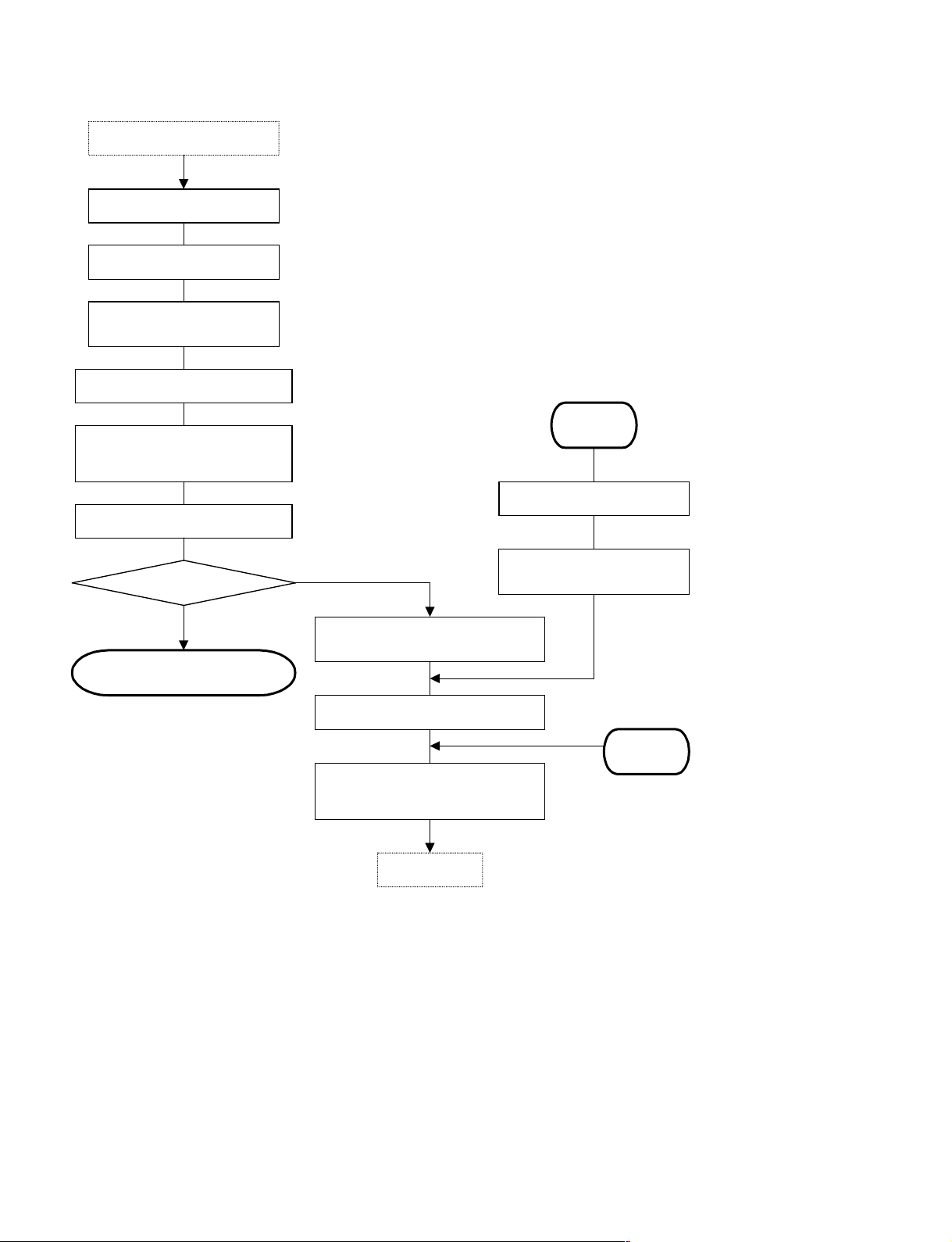
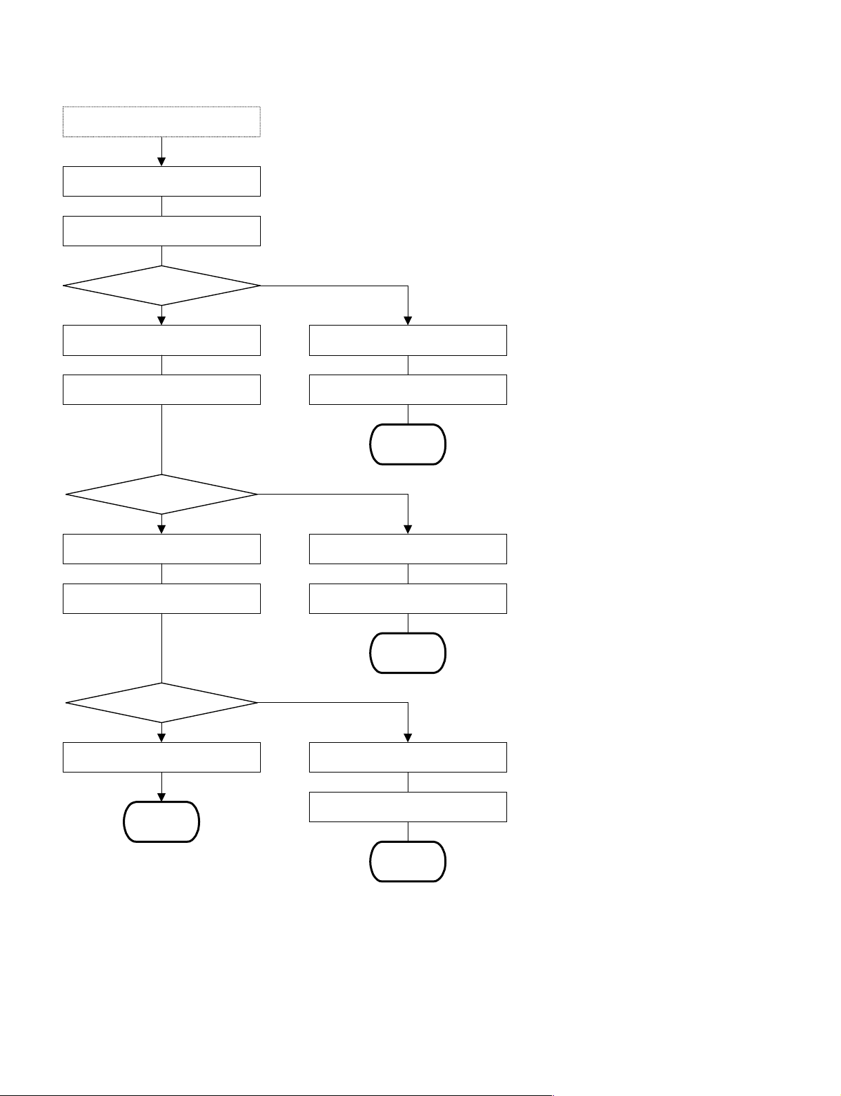
Non-recurrent analysis / Shipping mode
Non-recurrent analysis
From P2-13
Tapping on each PC board
* P-1 to P-5 : See the3-10 (P3-18)
P-1
Trouble reproduction?
External power OFF
Change the defective PC board
Analysis A
Go to P2-4
Yes
No
ROM version No. check
P-2
ROM version No. OK?
Yes
Ve readjustment
VE=16V ±0.1V
External power OFF / Separation
Leave the unit for 4 hours after
installing the running device.
No
ROM version up
PFM-500A1WU/500A1WE
P-3
Trouble reproduction? Go to P2-26
Yes
Analysis B
Go to P2-4
No
2-25
Page 36

From P2-25
Shipping
From P2-2, P2-14
P-5
Connections to power supply for exclusive use.
Install in test equipment.
APC function ON / Special power ON
Display test
P-4
OK?
Yes
Non-recurrent and returned unit?
Ye
No
s
Analysis B
Go to P2-4
No
2-26
Shipping substitute
Repair completed
(Shipping)
PFM-500A1WU/500A1WE
Page 37

3. Data
3-1. Check Point (X-SUS)
* V sync
X-SUS
1/8SF 2/8SF 3/8SF 6/8SF 7/8SF 8/8SF
Figure-1
DOYSD
Figure-2
DO YSU / F. VCC (=D OY SU+1 0V )
(DOXO)
Vs
0v
Vsc
EVEN ODD
+Va
0v (DOXE)
EVEN ODD
SUS
Vsw (350V)
PFM-500A1WU/500A1WE
Figure-3
_
Vs
0v
Vy
3-1
Page 38

3-2. Check Point (Y-COM)
Figure-4
GND
Vsc
_Vy
1 Frame
SUS (Vs)
240 240
EVEN LINE
1 Line selected signal (1/480)
Measurement point
ODD LINE
Y-COM
YCOMDV
Check-terminal
M1
M4
CN43CN46
YCN
YSUS PC board
FVCC
CN43 A1-A6
B1-B6
DOYSU
CN43 A13-A25
DOYSD
CN43 A28-A45
XSUS PC board
B13-B25
B28-B45
CN51
CN
CN53
X-BUS
XBUS
Measurement position
DOXO
A01-A21
CN53
B01-B21
DOXE
CN53
A25-A45
B25-B45
3-2
PFM-500A1WU/500A1WE
Page 39

3-3. Check Point (DC/DC)
Q31
T2
C41
C31
T1
C21
CN28
VW
CN33
C13
CN27
CN29
CN39
CN30
Voltage Circuit Adjustment point Set point Measurement point Measurement device
_Vy VR41 _Vy volume 160V ~ 180V ±1 % 3 digital multimeter
Ve VR61 Ve volume 16V ±0.1V 4 digital multimeter
Vrs VR54 Vrs volume 0 ~ 2V 5 digital multimeter
Vsc __ 100V ±0.1 % 1 digital multimeter
Vw __ 170V ±0.1 % 6 digital multimeter
C55
VSC
C75
G_4
IC81
CN37
1 Vsc Point
_
VY
2 GND Terminal
IC41
_VY
VR41
CN20
3 _Vy Point
C93
IC71
VR61
CN38
C54
VW
VR21
CN25
4 Ve Point 5 Vrs Point 6 Vw Point
VE
VRS
CN32
VR54
Vrs
CN24
CN31
C3
C1
C11
CN23
* Measurement point of Vsc : Vsc point and _Vy point.
PFM-500A1WU/500A1WE
3-3
Page 40

3-4. Check Point of Voltage (X-SUS, Y-SUS)
M6
M7
M16
M14
M8
M9
YSUS PC board
M10
M11
M12
M13
M3
M2
M1
CN41
CN42
M5
CN40
CN51
CN48
CN49
M13
M14
M4
M2
M1
M15
M16
XSUS PC board
M9
M11
M12
M5
M6M10
M17
M7
M8
18
19
20
10
M1
LV244
VH 32 VH 35
R13
R14
VH 33
2
1
M5
MB3615
R16
R15
VH 34
10
1
2
LV244
VH 27
VH 28
M1
20
19
18
R3 R6
R4 R5
C9
M4
MB3615
VH 30
VH 29
3-4
PFM-500A1WU/500A1WE
Page 41

3-5. Glossary
Oscilloscope : A device that allows the flow and strength of the running current to be visually
checked and measured.
Gradation : Shading of the display color.
External power ON : Running the external powers (Vcc. Va. Vs) on the designated voltage, unless
otherwise specified.
External power OFF : Making the external powers (Vcc. Va. Vs) to stop their operation completely,
unless otherwise specified.
White solid : A condition when the screen display is entirely white.
Tapping : Light impact.
Panel : The indication part of the plasma display panel (PDP).
Parts : Each PC board and parts mounted in the PC boards.
Panel voltage : The voltage required to operate the PDP normally.
Burn-in rack : Test equipment of the shelf test in which the PDP unit is left to stand in drive
condition.
Flexible cable : The cable for connecting the electric circuit to the panel.
Flicker : Continuous switching between bright and dark views by the PDP itself.
Protection cover : A cover made by aluminum to protect the PDP entirely during test.
Probe : A cable with contact finger that can transfer the status of the electric circuit to be
measured to an oscilloscope.
Remote control box : The device that can control the power on/off state of the power supply for
exclusive use (FPF10P-AC100/240B).
Unit of COM : The unit of circuits connected to the panel with flexible cable.
(YCOM UP/DOWN, XBUS UP/DOWN, address sections, the unit of PC boards
in ACOM1 to 5)
CPU : The unit for controlling the circuit operation.
DOYSU : Used in the drive voltage in the Y direction.
DOYSD : Used in the drive voltage in the Y direction.
DOXE : The control voltage for even-numbered lines in the X direction.
DOXO : The control voltage for odd-numbered lines in the X direction.
PUMP : The name of a circuit where the current from X/YSUS is returned.
PDP : Plasma display panel abbreviated.
ROM : Memory that stores the drive sequence and other data.
SUS : XSUS or YSUS.
Vcc : The power supply at 5 V, which is used to operate the logic section mainly.
Va : The power supply at 60 V, which is used to write data on the panel.
Vs : The power supply ranging from 127 V to 180 V, which is used to maintain
display data. In addition, this can serve as the primary side for the secondary
voltage (Vw, _Vy, Vsc).
XSUS: The name of the circuit that controls the panel operation in the X direction.
YCOMDV: The name of the panel drives voltage signal output from YCOM UP/DOWN
section.
YCOM: The circuit used to output a panel Y line selection signal and the voltage of a
display data keep signal.
YSUS: The name of the circuit that controls the panel operation in the Y direction.
PFM-500A1WU/500A1WE
3-5
Page 42

3-6. Connection to Test Equipment
PDP fixing jig
VG-826 remote control box
Function SW/RB-614C
Vcc/Va/Vs power supply
Power supply for exclusive use
Mount a protection cover on the PDP.
In case of an external power supply
Check that each power supply is turned off. Check that the remote control box switch is turned off.
Set the PDP on the PDP fixing tool of the test equipment and
connect a signal cable from the remote control box to CN1 on the logic PC board.
Connect the connector from the external
power supply to the DC/DC PC board
(CN23/CN24).
Each process Each process
In case of a power supply for exclusive use
Connect the connector from power supply to the
DC/DC PC board (CN23 to CN25).
Connection cable at 100VAC
3-6
PFM-500A1WU/500A1WE
Page 43

3-7. Test Equipment
6
5
7
4
3
1
2
4
5
6
Function
SW
VG-826
Remote control box
7
RB-614C
1 2
Vc Power supply Va Power supply
3
Vs Power supply
External power supply
PFM-500A1WU/500A1WE
3-7
Page 44

3-8. Photo (Burn-in Unit)
Burn-in equipment
3-8
Signal generator
PFM-500A1WU/500A1WE
Page 45

3-9. Burn-in Unit Instruction Manual
This manual explains the procedure of connecting the Burn-in unit and outlines the basic operations only
in the PDP signal generator.
Usage condition : AC input : 240 VAC
No. of running units : maximum of 2
I. Configuration
1. Power controller
1 AC power supply ON/OFF switch x 1 (breaker EG32F)
2 Individual power supply ON/OFF switch x 2 (FRONT, REAR)
2. Signal generator (1)
3. Individual power supply for exclusive use (2)
4. Cabinet (with PDP stand)
II. Names and Operations of Parts in Signal Generator
1. POWER switch
This switch can turn ON/OFF the external power supply.
2. Keyboard
This is used to set various functions.
3. Indicator
This is used to display the current operating status and data entered from the keyboard.
4. Output 1 to 4 ON/OFF switch (correspond to output 1 to 4)
This switch can turn ON/OFF the external output.
5. Output monitor LED (display the operating status. )
1 Output 1 to 4
2 R, G, B, (ON/OFF)
3 Reverse indication (ON/OFF)
4 DISP-ENB (Hi/Low)
5 Gradation status
16 steps 64 steps 256 steps
LED 1
LED 2
OFF
ON
6 Hi-QUALITY (Hi/Low)
7 TEST (Hi/Low)
III. Connection
1 Mount a protection cover on the PDP.
2 Check that the AC power supply switch and individual power switch in the burn-in unit are turned
off.
3 Connect AC cable from the burn-in unit to 240VAC.
4 Install the PDP on the stand of the unit and fix it.
5 Connect output cable from the power supply for exclusive use to DC/DC connector of PDP
(CN23 to 25).
6 Connect signal cable from the signal generator to CN1 in the logic section of PDP.
7 Turn on the AC power supply switch in the burn-in unit.
8 Turn on the power switch in the signal generator.
9 Turn on the power switch of the installed side -- FRONT or REAR.
Operation start
PFM-500A1WU/500A1WE
3-9
Page 46

IV. Changing and Selecting the Screen Display
The PDP unit enables the selection of 15 different patterns below. In addition, self test can be conducted
in any display pattern.
1. Available patterns and operations
Pattern No. Display pattern Pattern No. Display pattern
00 Automatic operation 09 Slant 8-color bar, vertical scroll
01 All solid 10 Cell plaid pattern
02 Vertical pattern 11 Most outer periphery frame + slant slash
03 Horizontal pattern 12 16 blocks
04 Plaid pattern 13 Vertical band
05 Vertical gradation 14 Lateral band
06 Horizontal gradation 15 Cross line
07 Vertical 8-color bar 16 Cross dot
08 Horizontal 8-color bar 17 _
2. Selecting the display pattern (for example, white solid pattern)
Key entry
Monitor indicator
Select
Pattern
0
1
Set
0 8 3 2 0 0 0 0
P T N 0 8
Operation mode indicator
P T N 0 0
P T N 0 1
0 8 3 2 0 0 0 0
Display pattern selection input field
(Select from the above table)
As the results of this operation, the PDP screen will be displayed in “white solid” pattern.
Any other pattern can be selected by entering the desired pattern No. (01 to 16) in the display Selection
field.
3-10
PFM-500A1WU/500A1WE
Page 47

3. Automatice display setting (used for running test)
Select
Display time
X
Set
(Automatic operation flow)
Select automatic display
Slant 8-color bar, vertical scroll display
XXXX second
White solid display
0 8 3 2 0 0 0 0
T I M 1 2 0 0
T I M X X X X
0 8 3 2 0 0 0 0
Current time (in sec)
Switching time input (0 to 3600 seconds)
Consecutive 75 hours
4. Palette setting
The gradation of all display colors can be checked with this setting.
0 8 3 2 0 0 0 0
P L A 0
OR 1
P L A 0 R 2 5 5
Indication and input area of current step No.(0 to 255)
Vary as instructed(R, B, and B)
P L A 0 R X X X
Input any value (0 to 255)
0 8 3 2 0 0 0 0
OR
Select
Pallet 0
R
OR
X
Set
G
B
PFM-500A1WU/500A1WE
3-11
Page 48

5. RGB ON/OFF
The indication of each color can be set to disable (used for checking a single color).
Select
3
R
G
OR
B
OR
Set
6. Function setting
Select
7
0 8 3 2 0 0 0 0
O N
R O N
Selected color
R O F F
0 8 3 2 0 0 0 0
0 8 3 2 0 0 0 0
D S E H I
/
O F F
Status of the display color (ON or OFF)
Vary as instructed
Current LED status
DISP ENB
HI LO
OR
4
OR
0
Set
H Q E L O
T S L O
D S E L O
Press
0 8 3 2 0 0 0 0
key to display HI and LO alternately
HI-QEN
HI LO
TEST
HI
HI
LO
DISP ENB
LO
3-12
PFM-500A1WU/500A1WE
Page 49

3-10. Criteria Table
(Scope : UD-01)
Item P2-3, 4 Judgment
No. Branch condition YES NO
A-1 Operation OK? The fan of the signal generator rotates, The fan of the signal generator does not
A-2 AC100V OK? Measured with Digital bottle-meter, AC100V isn’t input..
A-3 Appearance OK? The product is regarded to Product with defect in appearance
A-4 Screen lighting? Some data is displayed on the screen.
and the LED display is 001. rotate, and the LED display is not 001.
and AC100V is input..
operate normally because it does YCOM failure (hole)
not show any defect in Panel failure (fracture, crack of chip pipe)
appearance as mentioned above. Flexible cable failure
(break, peeling, and others)
In particular, check the panel to
see if there are any cracks in the
corner (gas leak)
Blur, flow, parts failure, missing
parts, disconnection of cable,
and other defects in appearance
may affect PDP operation.
(The background light emission is included.) No data is displayed on the screen.
Item P2-5, 6 Judgment
No. Branch condition YES NO
B-1 Overcurrent? Icc>2.5 Icc<2.5
B-2 Overcurrent? Icc>2.5 Icc<2.5
B-3 Vcc or Va checks? Abnormal check of VCC and Va. Checks other than Vcc and Va.
B-4 XSUS or YSUS XSUS or YSUS is separated. XSUS or YSUS is not separated.
Separated?
B-5 Overcurrent? Ia>0.2(A) Ia<0.2(A)
B-6 Overcurrent? Is>3.5(A) Is<3.5(A)
B-7 YCOM PC board Separated because CN46 and CN47 on Not separated because YCOM UP and
Separated? YCOM UP and DOWN sections are DOWN both or either section is connected
disconnected from CN43 and CN44 to CN43 or CN44 on YSUS.
on YSUS.
B-8 YCOM Separated because CN46 and CN47 on Not separated because YCOM UP and
separated? YCOM UP and DOWN sections are DOWN both or either section is connected
B-9 SUS separated? The power connectors CN49 and CN50 XSUS and YSUS are not separated from
B-!/ Screen flicker OK? PDP shows bright (turn on) and Abnormal condition, not showing the right
B-!- Any data display Some data is displayed on the screen. No data is displayed on the screen.
disconnected from CN43 and CN44 to CN43 or CN44 on YSUS.
on YSUS.
for XSUS or the power connectors CN41 DC/DC.
and CN42 for YSUS are disconnected from
DC/DC connector.
dark (turn off) views alternately condition
on the entire screen.
PFM-500A1WU/500A1WE
3-13
Page 50

(Scope : UD-01)
Item P2-7, 8 Judgment
No. Branch condition YES NO
C-1 Separate the XSUS The power connectors CN49 and CN50 for The power connectors CN49 and CN50 for
PC board? XSUS are disconnected from XSUS are not disconnected from
C-2 Separate the YSUS The power connectors CN41 and CN42 for The power connectors CN41 and CN42 for
PC board? YSUS are disconnected from YSUS are not disconnected from
C-3 Overcurrent? Icc>1.7(A) Icc<1.7(A)
C-4 Overcurrent? Ia>0.2(A) Ia<0.2(A)
C-5 Overcurrent? Is>0(A) Is=0
C-6 Overcurrent? Icc>1.7(A) Icc<1.7(A)
C-7 Overcurrent? Icc>1.7(A) Icc<1.7(A)
C-8 Overcurrent? Icc>1.7(A) Icc<1.7(A)
Item P2-9, 10 Judgment
No. Branch condition YES NO
D-1
Measurement OK?
D-2
Measurement OK?
D-3
Measurement OK?
D-4
Measurement OK?
D-5
Measurement OK?
D-6
Measurement OK?
D-7
Measurement OK?
D-8
Measurement OK?
D-9 DC/DC changed Changed DC/DC supply already. Not changed DC/DC supply.
already?
the DC/DC connector. the DC/DC connector.
the DC/DC connector. the DC/DC connector.
VH27<1.8 or VH27>1.3 VH27>1.8 or VH27<1.3
VH32<1.8 or VH32>1.3 VH32>1.8 or VH32<1.3
VH28<1.8 or VH28>1.3 VH28>1.8 or VH28<1.3
VH33<1.8 or VH33>1.3 VH33>1.8 or VH33<1.3
VH29<1.8 or VH29>1.3 VH29>1.8 or VH29<1.3
VH34<1.8 or VH34>1.3 VH34>1.8 or VH34<1.3
VH30<1.8 or VH30>1.3 VH30>1.8 or VH30<1.3
VH35<1.8 or VH35>1.3 VH35>1.8 or VH35<1.3
3-14
PFM-500A1WU/500A1WE
Page 51

(Scope : UD-01)
Item P2-11, 12 Judgment
No. Branch condition YES NO
E-1 Display OK? The screen is all white color display. Display omission in white color display.
E-2 New panel? Already changed due to a defective panel. Not changed.
E-3 APC OK? APC Operations normal. APC Operations is abnormal.
E-4 Display OK? A surplus, a defect, a step, A surplus, a defect, a step, and a tone
E-5 Logic PC board Changed Logic PC board already. Not Changed Logic PC board.
Changed?
E-6 New LBUS? Changed LBUS PC board already. Not changed LBUS PC board.
E-7 Changed? Changed Logic PC board already. Not changed Logic PC board.
E-8 Lateral display Found display error in the lateral direction No display error in the lateral direction.
error? on the screen.
E-9 Waveform OK? Upon monitoring the waveform output Upon monitoring the waveform output
E-!/ Waveform OK? YSUS waveform is normal. YSUS waveform is abnormal.
E-!- Failure caused by Panel failure caused by display cell Panel failure not caused by display cell
panel error? defect and brightness variation defect and brightness variation
and a tone operation are normal. operation are abnormal.
(For example, lack of indication or fringes
in the lateral direction.
from DOXE and DOXO for XSUS, from DOXE and DOXO for XSUS,
it was found that waveforms on EVEN an inclination (not level) was found on
and ODD at around 50(V) are even. EVEN and ODD at around 50(V).
In addition, other abnormal waveforms Alternatively, some abnormal waveforms
were not found. were found.
in the panel. in the panel.
Item P2-13, 14 Judgment
No. Branch condition YES NO
F-1 Non-recurrent The fault did not recur. The specified fault recurred.
product?
F-2 Faults recur? The fault does not recur upon The fault does not recur upon
re-installation of new parts. re-installation of new parts.
F-3 ROM version No. The ROM installed are listed in The ROM installed is not listed in
OK? the table below. the table to the left.
Model UD01
ROM 197 or 197G
F-4 Display operation Not found abnormality or failure in Found abnormality or failure in the display
OK? the display operation. operation.
PFM-500A1WU/500A1WE
3-15
Page 52

(Scope : UD-01)
tem P2-15 Judgment
No. Branch condition YES NO
G-1 ACOM Found abnormality in a single A-COM unit Not found abnormality such as vertical line,
PC board unit? (one-fifth of screen width) or more. vertical band, and vertical fringe in the
G-2 Single line missing Found abnormality in one line or band. Found abnormality in two or more lines or
G-3 Fuse blown? Fuse is blown (not conductive). Fuse is not blown (conductive).
The tester reads ∞ ohm in one range. The tester reads 0 ohm in one range.
G-4 Regularity? Found some regularity for display error in No regular recurrence of display errors in
vertical direction -- at a certain interval, the vertical direction.
and others.
G-5 BUS board Changed BUS board already Not changed BUS board
changed?
Item P2-16, 17 Judgment
No. Branch condition YES NO
H-1 Connector OK? The cards for A-COM1 to 5 are The cards for A-COM1 to 5 are discon-
connected to RBUS, LBUS, nected from RBUS, LBUS, or
and logic PC boards properly. logic PC board or not connected properly.
H-2 Chip OK? Found no ACOM chip failure in Found ACOM chip failure in visual
visual checking. checking.
H-3 Fuse changed? Changed fuse already. Not changed fuse.
H-4 Fuse blown? Fuse is blown (not conductive). Fuse is not blown (conductive).
The tester reads ∞ ohm in one range. The tester reads 0 ohm in one range.
H-5 RBUS changed? Changed RBUS PC board already. Not changed RBUS PC board.
H-6 Logic changed? Changed Logic PC board already. Not changed Logic PC board.
H-7 LBUS changed? Changed LBUS PC board already. Not changed LBUS PC board.
ACOM unit (one-fifth of screen width).
bands.
Item P2-18 Judgment
No. Branch condition YES NO
K-1 Both SUS? Likely failure in both XSUS and YSUS. Failure in either XSUS or YSUS.
K-2 XSUS? XSUS failure (waveform). YSUS failure (waveform).
K-3 Changed? Changed logic PC board already. Not changed Logic PC board.
K-4 Changed? Changed XSUS PC board already. Not changed XSUS PC board.
K-5 Changed? Changed YSUS PC board already. Not changed YSUS PC board.
K-6 Output OK? Ve 16 V ~ 18 V ±0.1 % ,Vsc 100 V ±0.1 % The voltage (Ve, Vsc., Vw, _Vy) do not
Vw 180 V ±0.1 % , _Vy 170 ~ 180 ±1.0 % indicate the values as
mentioned on the right.
3-16
PFM-500A1WU/500A1WE
Page 53

(Scope : UD-01)
Item P2-19, 20 Judgment
No. Branch condition YES NO
L-1 Light emission Found light emission from background. Not found light emission from background.
from background?
L-2 Output OK? Ve output is Ve>16 and Ve<18. Ve output is Ve<16 and Ve>18.
L-3 Waveform OK? An output waveform shown by figure 1,2 It isn’t an output waveform shown by figure
L-4 Output OK? YCOMDV output is normal. YCOMDV output is abnormal. (see the
L-5 Output OK? An output shown by figure 1 of appendix 1. It Isn’t an output shown by figure 1 of
L-6 Waveform A? An output waveform (A) shown by An output waveform (B) shown by flow
L-7 Changed? Changed XSUS PC board already. Not changed XSUS PC board.
L-8 Changed? Not changed YSUS PC board. Changed YSUS PC board already.
Item P2-21, 22 Judgment
No. Branch condition YES NO
M-1 Input OK? Found VPON entry (XSUS). Not found VPON entry (XSUS).
M-2 Input OK? Found VPON entry (YSUS). Not found VPON entry (YSUS).
M-3 VEGO OK? After YEGO outputs about 120ms Excluding the left
M-4 VWYGO OK? After VWYGO outputs about 120ms Excluding the left
M-5 Always “0”? A logical output is always “0” A logical output is not “0”
and 3 of appendix 1,2. 1,2 and 3 of appendix 1,2.
(see the figure 4 of appendix 2) figure 4 of appendix 2)
appendix 1.
flow chart. chart.
and about 5 V, YEGO becomes 0V.
and about 5 V, VWYGO becomes 0V.
PFM-500A1WU/500A1WE
3-17
Page 54

(Scope: UD-01)
Item P2-23, 24 Judgment
No. Branch condition YES NO
N-1 Output OK? VH27<1.8 or VH27>1.3 VH27>1.8 or VH27<1.3
N-2 Output OK? VH32<1.8 or VH32>1.3 VH32>1.8 or VH32<1.3
N-3 Output OK? VH28<1.8 or VH28>1.3 VH28>1.8 or VH28<1.3
N-4 Output OK? VH33<1.8 or VH33>1.3 VH33>1.8 or VH33<1.3
N-5 Output OK? VH29<1.8 or VH29>1.3 VH29>1.8 or VH29<1.3
N-6 Output OK? VH34<1.8 or VH34>1.3 VH34>1.8 or VH34<1.3
N-7 Output OK? VH30<1.8 or VH30>1.3 VH30>1.8 or VH30<1.3
N-8 Output OK? VH35<1.8 or VH35>1.3 VH35>1.8 or VH35<1.3
Item P2-25, 26 Judgment
No. Branch condition YES NO
P-1 Trouble The fault recurred. The specified fault does not recur.
reproduction?
P-2 ROM The ROM installed are listed The ROM installed is not listed
version No. OK? in the table below. in the table to the left.
Model UD01
ROM 197L or 197G
P-3 Trouble Some problem occurred or the fault Any fault including the specified fault does
reproduction? recurred during running test. not occur.
P-4 OK? The PDP function works perfectly normal. Some fault or problem occurred.
P-5 Non-recurrent The PDP unit, which was once returned Not returned due to the same fault in the
and due to a fault, has been inspected and same position as before.
returned unit? shipped following no recurrence of the fault.
Then, the unit was returned again with
the same fault. However, the faulty part
cannot be isolated because the fault
has not recurred yet.
3-18
PFM-500A1WU/500A1WE
Page 55

3-11. Voltage Setting Procedure
Vs and _Vy fluctuation, voltage margin is measured and a set voltage is decided. Use the external and
internal (DC/DC in 3-3) power supplies to generate +Vs and _Vy respectively.
Please see to Display Test Manual (3-12) for each display pattern.
1. Panel Voltage Measuring Procedure
Judgment of the minimum voltage : The level at which every point is turned on upon raising the voltage
slowly at each point (except the special points).
Special point : The point that is not turned on when every other point is turned on.
This point requires a higher voltage to be turned on.
Judgment of the maximum voltage : The level at which the surplus points are disappeared with a straight
change in voltage upon lowering the voltage slowly at each point.
Surplus point : The display point other than display data
(Except constant surplus point).
(Procedure) (Operation)
1 Preparation Install and turn on the test equipment in the white solid display in the
highest level for four minutes.
2 Vs(min) setting _Vy = _160 V (Temporary setting)
Setting : APC : ON, HQEN : OFF
Display : Gray-scale [R16 gradation : Left discernment-Right privily]
Cross-hatch + slash-pattern (G The highest gradation)
3 Vs Set value Decision [The set value of Vs is decided from Vs (min) in this paragraph.]
Vs (min)=Vs (min) +4 V
(1) For Vs (min)<180 V/Vs(Set value)=180 V
(2) At setting Vs = 180 V, Margin measurement in clause 4-7.
When abnormality is found in the display confirmation, VS is
assumed 170 V, and executes clause 4-7. But, it is assumed Vs
(min) <170 V.
4 _Vy Margin measurement [Set value as for Vs. _Vy margin is measured in this paragraph.]
Setting : APC : ON, HQEN : OFF
Display : _Vy (min) : Overall lighting
(W, R, G, B Each color highest gradation)
Cross-hatch +slash-pattern (G The highest
gradation)
_Vy (max) : Overall lighting (W The highest gradation)
Gray-scale
[R, G, B Each color 16 gradation :
Left discernment-Right privily]
Length color bar
[R=172, G=192, B=255 Each color specification
gradation (50 Hz)]
Cross-hatch + slash-pattern
(W The highest gradation)
Next page
PFM-500A1WU/500A1WE
3-19
Page 56

Before page
5 _Vy Set value Decision [The set value of _Vy from _Vy margin is decided in this paragraph.]
(1) _Vy (Set value) = _Vy _4 V
But, for a | _Vy (Set value) |<| _145 V|, _Vy(Set value) _145
(2) _Vy (Set value) _4V<_Vy (max)
6 Margin confirmation [The Vs margin is finally set by the result of the _Vy setting.]
Vs (min) is confirmed with Vs _3V.
Vs (max) is confirmed with Vs +4V.
Setting : APC : ON, HQEN : OFF
Display : _Vy (min) : Overall lighting (B The highest gradation)
Gray-scale
[R, G, B Each color 16 gradation :
Left discernment-Right privily]
Cross-hatch +slash-pattern
[W, R, G, B Each color highest gradation)
_Vy (max) : Overall lighting (W The highest gradation)
Gray-scale
[R, G, B each color 16 gradation :
Left discernment-Right privily]
Length color bar
[R = 172, G = 192, B = 255 Each color specification gradation (50 Hz)]
7 Display confirmation [The display confirmation of Vs and _Vy is done by the set value.]
Setting : APC : ON, HQEN : OFF
But, gradation plover pattern HQEN : ON
Display : Length belt pattern
[R : 134 & 136] AUTO program mode test (10 cycle)
[See the next page]
Gradation plover pattern [G : 62 & 64]
Length color bar
[R = 172, G = 192, B = 255 Each color specification gradation
(50 Hz)]
Gray-scale
[R, G, B Each color 16 gradation : Left discernment-Right
privily]
Length belt pattern and gradation plover pattern are numbers 0 of
blinking faults. But, the cell defect-blinking fault is excluded.
Length belt pattern and gray-scale are five pixel or less of blinking
faults.
But, the cell defect-blinking fault is excluded. (Self-erase judgment :
SE)
3-20
PFM-500A1WU/500A1WE
Page 57

AUTO Program Mode Test (Operation and Stop Procedure)
Purpose : Black point noise Evaluation pattern (No.22 . 23) is alternately displayed, and the presence of
Black point noise is confirmed.
Method : The undermentioned operation is executed from RB-614C keyboard.
FUNC Key PUSH
1
SET
SET
Program No.22
Black Point Pattern display
Program No.23
Black Point Pattern display
FUNC push?
Yes
Program No.22
Black Point Pattern display
Key PUSH
Key PUSH
Key PUSH
No
Keeps pushing for about 3 seconds.
0
SET
AUTO Program Mode STOP
Arbitrary key
PFM-500A1WU/500A1WE
Key PUSH
Key PUSH
3-21
Page 58

Marginal diagram (reference drawing for setting voltage when Vs=180V)
Vs (v)
185
180
175
170
-Vs min-4V
Vs Set value
-Vs min
-Vy Set value
Check point Vs max (Vs +4 V)
Check point -Vy (Set value = _4 V)
Check point Vs min(Vs _3 V)
Vs min
_160
_Vy max
_170_150 _152 _156
Area which can be set
DC/DC internal voltage setting (see the 3-3 for the measuring points for Vrs, _Vy voltages)
1 Connect the external power supply to CN23 to 25 on the DC/DC PC board.
2 Set a digital multimeter to the voltage of Vrs on the DC/DC PC board.
3 Turn on the external power supply.
_Vy (v)
4 Set to the voltage of Vrs on the DC/DC PC board. (Vs formula : Vs = 165 +10xVrs, Vrs = 0 to 2.0 V)
5 Set the marginal value to _Vy.
6 Complete setting after display test.
3-22
PFM-500A1WU/500A1WE
Page 59

2. Voltage Setting Procedure in Replacement of the DC/DC
Measure the voltage on the old DC/DC PC board and set the measurement on the new voltage.
Measuring points and setting voltage
1 Vrs voltage
2 _Vy setting voltage
Setting procedure when an invalid voltage exists
1 Set Vs to 180 V.
2 Set _Vy to 160 V and perform the display operation to check if the resulting value is valid with the
table as shown below. Obtain the setting voltage by fluctuating the value within the standard electric
potential and set this value.
PFM-500A1WU/500A1WE
3-23
Page 60

3-12. Display Test Manual
This manual explains the examination procedure and the operation method when 42-model PDP is
examined by using VG-826. The display pattern is recorded. The display function of PDP is confirmed.
1. Signal generator
VG-826 is used as a display signal generator. The display pattern is built into panel ROM by the program
form. The program No. is selected from the keyboard, and the display function is confirmed.
Signal generator
External keyboard (RB-614C)
Ten-key for program No. input
Exclusive pattern-key
FUNCTION-key
Panel ROM
2. Panel ROM and External keyboard
In ROM, there is a test pattern for a lot of displays. The selection of the test pattern inputs the figure of
two digits (01 ~ 36) by External keyboard.
This program is a display test pattern to examine the PDP-unit connected with VG-826. The display
pattern for this test is in program ROM.
Mount panel ROM so that VG-826 may operate by the program data.
1 Panel ROM
Memory of display data as program
Selection program ....... 36 pattern
2 RB-614C External keyboard function
Key name Number Key-function
Fixed display exclusive key 11 A fixed pattern is displayed.
Option-key 1 1 23 kinds of patterns can be displayed.
Option-key 2 1 23 kinds of patterns can be displayed.
FUNCTION 1 VG-826 Function selection key (Unused usually)
SET 1 Key which effectively does function selection (Unused usually)
INV 1 The screen display is reversed.
R,G,B (Each) 3 The display of each color is switched.(ON / OFF)
H-T 1 Unused
&
3-24
PFM-500A1WU/500A1WE
Page 61

t
3. Test equipment connection diagram
Check whether the connection of the test equipment is normal, before doing trouble analysis and the
display test of the PDP device. (See the undermentioned connection diagram)
68 p connector
Logic (go to CN1)
To DC/DC CN24
34 line flat cable
APC D.EN HQEN B.CONT
OFF OFF OFF
8P connector
CN 4 CN5
CN6
flat cable
DIGITAL OUT
VG-826
DIGITAL
VIDEO
GENERATOR
50P
flat cable
3
CN
Remote Control BOX
POWER
POWER/SW
50P
AC100V
CN1 CN2
POWER OFF 0
POWER ON 1
REMOTE
3P DC24 V
2
CN
MAIN SW BOX
OFF
(AC100V)
o
(AC240V)
INC DEC SET
RB-614C
PDP Special power
supply
To DC/DC CN25
To DC/DC CN26
To DC/DC CN25
To DC/DC CN26
9P connector
10P connector
9P connector
10Pconnector
ROM
LED display window
External power supply
Vcc Va Vs
(FPF10P-AC100/240B)
AC100 V
PFM-500A1WU/500A1WE
3-25
Page 62

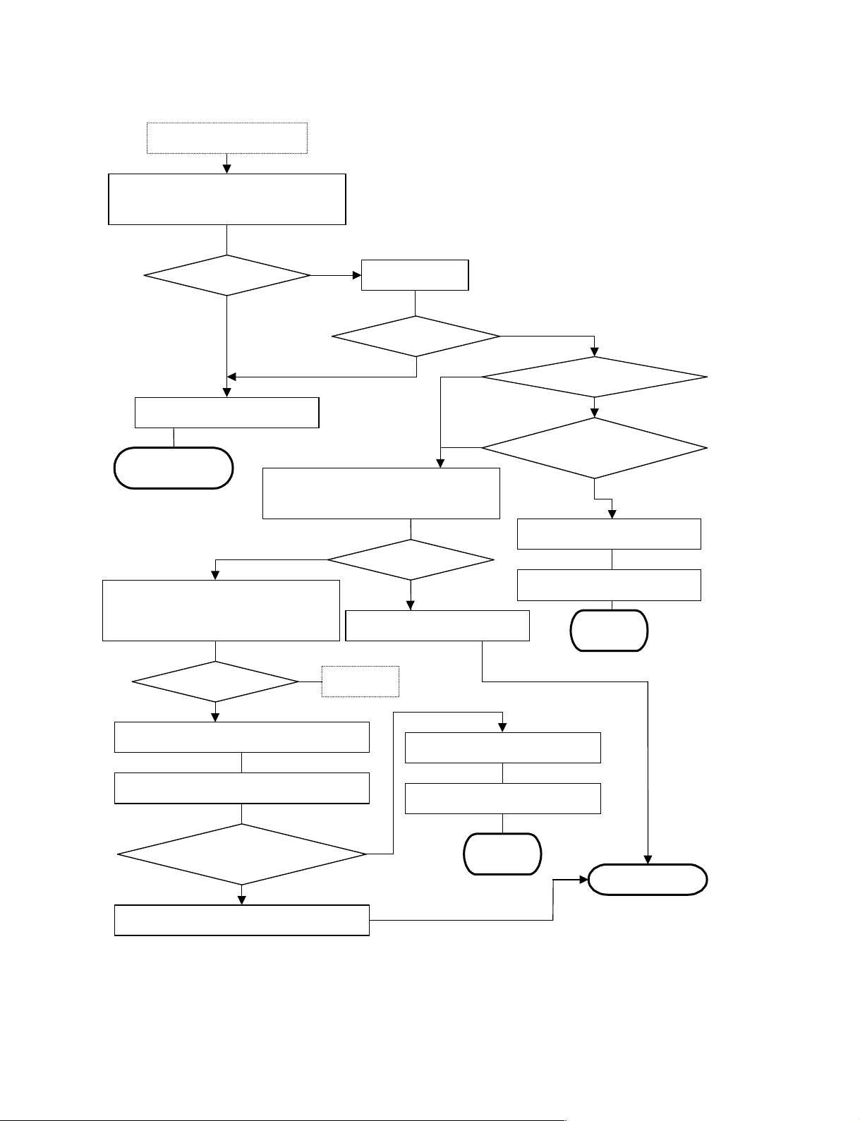
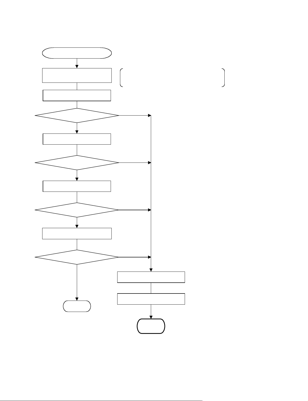
4. Test equipment Start procedure and Equipment connection
Each decision criteria is described to the attached paper. (See the 3-15)
Connection
Check MAIN SW OFF
A-1
MAIN SW OFF
Yes
Check VG-826 POWER SW OFF
A-2
POWER SW OFF
Yes
Test equipment power supply connection
Test equipment MAIN SW ON
VG-826 POWER SW ON
A-3
VG-826 Operation OK?
No
MAIN SW OFF
No
POWER SW OFF
No
Yes
68P connector is connected with
the logic part (CN1)
External power supply or Special power supply
cable is connected with DC/DC.
External power supply is connected individual SW
OFF is confirmed.
Equipment connection completion
3-26
VG-826 input check
A-4
AC input OK?
VG-826 Repair request
No
Yes
AC input improvement processing
Go to Connection
PFM-500A1WU/500A1WE
Page 63

5. Operation method and Display
1 Operation method
The signal generator enters command input standby by turning the POWER SW to ON.
RB-614C can select the display pattern by the input numerical value (01-36) of two digits from a numeric
key. (You can see the Display pattern on P3-28, 29.)
POWER ON
Command input standby
B-1
Input ?
Yes
Selection pattern display OK ?
Yes
No
No
PFM-500A1WU/500A1WE
3-27
Page 64

3-13. VG-826 Program Display Pattern
P-No. Color Display pattern P-No. Color Display pattern
01 W 16 W
02 R
03 G
04 B
One color on all screens display Discernment --- 256 gradation --- Privily
05 W 17 W
06 R 18 R
07 G 19 G
08 B 20 B
Lattice +Slash +Frame Window
09 W 21 W
Privily --- 256 gradation --- Discernment English
10 No display 22 R
11 W 23 R
12 R
13 G
14 B
Horizontal belt Length belt
15 W 24 G
The middle gradation display Gradation plover pattern
3-28
PFM-500A1WU/500A1WE
Page 65

P-No. Color Display pattern P-No. Color Display pattern
25 W 32 Mix
Length belt Color-bar
26 W 33 W
27 R 34 R
28 G 35 G
29 B 36 B
Frame +Slash Window
31 W
Half tone
PFM-500A1WU/500A1WE
3-29
Page 66

3-14. Fixed Display Exclusive-key Pattern
The thing to push an exclusive-key can display these screens.
CHARA CROSS DOT
CIRC COLOR GLAY
BRST
WINDOW
++
+
++
xx
x
xx
3-30
PFM-500A1WU/500A1WE
Page 67

3-15. Decision Criteria Table (Object Page : P3-26, 27)
YES NO
A-1 MAIN SW OFF MAIN SW ON
A-2 VG-826 POWER SW OFF VG-826 POWER SW ON
A-3 The fan of the signal generator (VG-826) rotates, The fan of the signal generator (VG-826) doesn’t
and the LED display is 001. rotate. /LED is not displayed.
A-4 AC100V is input. AC100V is not input.
B-1 Two-digit numerical value to 01-36 is input. Numerical values other than the left were input.
PFM-500A1WU/500A1WE
3-31
Page 68

3-16. PC Board Replacing Proceduce
Replacing-procedure of Print PC board is shown in the following. PC board replacing work after a
defective PC board separates works in reverse-procedure.
n
Please note insulating bushing position when you install PC-board.
Exchange PC board confirmation
Check each power supply OFF
XSUS PC board exchange
YSUS PC board exchange
CN48 to CN50
Separation
PC board fixation
screw detaching
screw (3 x12 mm) x10
Insulating bushing
UC-02 x9
Others x2
XSUS Separation of
connector
CN51-53/CN52-54
XSUS PC board
Separation
XSUS PC board
exchange
External power supply ?
Yes
Signal cable and power supply cables are separated.
PDP is moved to the work stand and the protecting cover is removed.
Defective PC board selection
DC/DC PC-board exchange
CN40 to CN42
Separation
PC board fixation
screw detaching
screw (3 x12mm) x10
Insulating bushing x10
UC-02 x10
Others x2
YSUS Separation of
connector
CN43-46/CN44-47
XSUS PC board
Separation
XSUS PC board
exchange
CN5, 9,11,13,37,41,42,49, 50
Each connector separation
PC board fixation
screw detaching
screw (3 x12mm) x 2
Thai lap cutting
(8 places)
DC/DC PC board
Separation
DC/DC PC
board exchange
No
Check Remote-Ctrl BOX SW OFF
Address PC board exchange
Logic PC board exchange
CN2 to 5, 16
Separation
Address PC board
Separation
PC board fixation
screw detaching
screw (3 x12mm) x2
Logic PC board
Separation
Logic PC board
exchange
L-BUS (CN13, 17,18)
Separation
R-BUS (CN11, 14,15)
Separation
Each ABUS PC board
PC board fixation
screw detaching
screw (3x20mm)x2
Connector separation
L-BUS (CN12-CN8)
separation
R-BUS (CN10-CN7)
separation
L or R-BUS PC board
Separation
Address PC board
exchange
3-32
PFM-500A1WU/500A1WE
Page 69

3-17. Each PC Board Installation Screw Position/Connector Position
UD-01
YCOM UP
CN
46
YCOM DOWN
CN
47
CN37
CN4 CN5
CN3
Logic PC board
CN18
DC/DC
CN25 CN24 CN23
9
CN
CN16
CN
CN
CN7
2
1
CN10
CN15
CN49
CN50
XSUS PC board
CN48
CN11
RBUS PC board
CN43
YSUS PC board
4
CN4
CN13
LBUS PC board
CN18
ACOM5 ACOM3ACOM4 ACOM2 ACOM1
CN41
CN42
CN40
PC board installation screw position
Insulating bushing (NA18100-X024) Installation screw position
With core (Cable with core)
CN26 CN37
CN12
CN17
CN51
CN52
CN14
XBUS UP
CN
53
XBUS DOWN
CN
54
PFM-500A1WU/500A1WE
3-33
Page 70

Page 71

The material contained in this manual consists of
information that is the property of Sony Corporation.
Sony Corporation expressly prohibits the duplication of
any portion of this manual or the use thereof for any
purpose other than the operation or maintenance of the
equipment described in this manual without the express
written permission of Sony Corporation.
Le matériel contenu dans ce manuel consiste en
informations qui sont la propriété de Sony Corporation.
Sony Corporation interdit formellement la copie de
quelque partie que ce soit de ce manuel ou son emploi
pour tout autre but que des opérations ou entretiens de
l’équipement à moins d’une permission écrite de Sony
Corporation.
Das in dieser Anleitung enthaltene Material besteht aus
Informationen, die Eigentum der Sony Corporation sind.
Die Sony Corporation untersagt ausdrücklich die
Vervielfältigung jeglicher Teile dieser Anleitung oder den
Gebrauch derselben für irgendeinen anderen Zweck als
die Bedienung oder Wartung der in dieser Anleitung
beschriebenen Ausrüstung ohne ausdrückliche
schriftliche Erlaubnis der Sony Corporation.
PFM-500A1WU/500A1WE
Page 72

Sony Corporation
B&P Company
©2001 FUJITSU HITACHI PLASMA DISPLAY LIMITED9-976-682-41
Printed in Japan
English
01HS16-1
©2001.8
 Loading...