

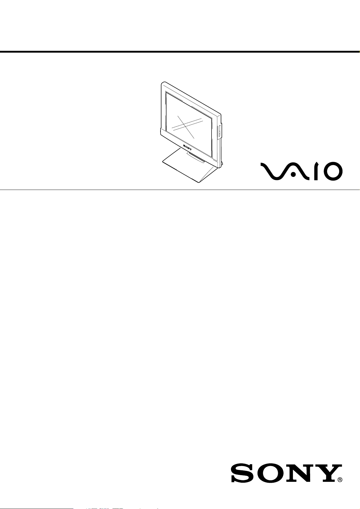
PCVA-15XD2
SERVICE MANUAL
SPECIFICATIONS
LCD panel
Panel type: a-Si TFT Active Matrix
Picture size: 15 inch (38cm)
Picture element: 99.99%
Resolution
Horizontal: Max. 1024 dots
Vertical: Max. 768 lines
Power requirements
— AC adapter
Input: AC 100 – 240V/
1A/50 – 60Hz
Output: DC 12V/3A
— LCD Display
Input: DC12V/1.7A
Power consumption
Max. 36W (less than 3W in power
saving mode)
Canadian Model
Dimensions (width/height/
depth)
Approx. 380 × 360 × 200 mm
1
7
/
× 7
(15 × 14
Mass
Approx. 5.5 kg (12 lb 2 oz)
Plug & Play
DDC1/DDC2B
Accessories
• LCD display
• AC adapter
• Power cord
• Warranty Card
• This instruction manual
Design and specifications are subject
to change without notice.
4
/8 inches)
US Model
9-928-380-11
15 INCH TFT LCD DIGITAL DISPLAY

Information in this document is subject to change without notice.
Sony and VAIO are trademarks of Sony. Intel logo and Intel Inside
logo are registered trademarks of Intel Corporation. Pentium MMX
is a trademark of Intel Corporation. Microsoft, MS-DOS, W indows,
the W indows 95 and W indows 98 log o are trademarks of Microsoft
Corporation.
All other trademarks are trademarks or registered trademarks of
their respective owners. Other tr ademarks and trade names may be
used in this document to refer to the entitles claiming the marks and
names or their produces. Sony Corporation disclaims any proprietary
interest in trademarks and trade names other than its own.
Caution Markings for Lithium/Ion Battery - The following or similar
texts shall be provided on battery pack of equipment or in both the
operating and the service instructions.
CAUTION: Danger of explosion if battery is incorrectly replaced.
Replace only with the same or equivalent type recommended by
the manufacturer. Discard used batteries according to the
manufacturer’s instructions.
CAUTION: The battery pack used in this de vice may present a f ire
or chemical burn hazard if mistreated. Do not disassemble, heat
above 100°C (212°F) or incinerate.
Dispose of used battery promptly.
Keep away from children.
Service and Inspection Precautions
1. Obey precautionary markings and instructions
Labels and stamps on the cabinet, chassis, and components identify areas
requiring special precautions. Be sure to observe these precautions, as well
as all precautions listed in the operating manual and other associated
documents.
2. Use designated parts only
The set’s components possess important safety characteristics, such as
noncombustibility and the ability to tolerate large voltages. Be sure that
replacement parts possess the same safety characteristics as the originals.
Also remember that the 0 mark, which appears in circuit diagrams and
parts lists, denotes components that have particularly important safety
functions; be extra sure to use only the designated components.
3. Always follow the original design when mounting
parts and routing wires
The original layout includes various safety features, such as inclusion of
insulating materials (tubes and tape) and the mounting of parts above the
printer board. In addition, internal wiring has been routed and clamped so
as to keep it away from hot or high-voltage parts. When mounting parts or
routing wires, therefore, be sure to duplicate the original layout.
4. Inspect after completing service
After servicing, inspect to make sure that all screws, components, and wiring
have been returned to their original condition. Also check the area around
the repair location to ensure that repair work has caused no damage, and
confirm safety.
5. When replacing chip components...
Never reuse components. Also remember that the negati ve side of tantalum
capacitors is easily damaged by heat.
6. When handling flexible print boards...
•The temperature of the soldering-iron tip should be about 270C.
•Do not apply the tip more than three times to the same pattern.
•Handle patterns with care; never apply force.
Caution: Remember that hard disk drives are easily damaged by
vibration. Always handle with care.
ATTENTION AU COMPOSANT AYANT RAPPORT
À LA SÉCURITÉ!
LES COMPOSANTS IDENTIFÉS P AR UNE MARQUE 0 SUR LES
DIAGRAMMES SCHÉMA TIQUES ET LA LISTE DES PIÈCES SONT
CRITIQUES POUR LA SÉCURITÉ DE FONCTIONNEMENT. NE
REMPLACER CES COMPOSANTS QUE PAR DES PIÈSES SONY
DONT LES NUMÉROS SONT DONNÉS DANS CE MANUEL OU
DANS LES SUPPÉMENTS PUBLIÉS PAR SONY.
Confidential
PCVA-15XD2 (UC)
— 2 —

TABLE OF CONTENTS
1. OVERVIEW ······························································1-1
2. DISASSEMBLY
2-1. Flowchart ·····································································2-1
2-2. Arm Rear Cover ···························································2-1
2-3. Arm Front Cover ··························································2-2
2-4. Rear Cover, Inverter Unit ·············································2-3
2-5. LCD Ass’y (S), LEX-23 Board···································· 2-4
2-6. IFX-105 Board ·····························································2-5
2-7. Main Electrical Parts Location Diagram······················2-5
3. SERVICE OVERVIEW
3-1. Service Tools································································ 3-1
3-2. Procedure For Writing Edid Data ································3-1
3-3. Procedure For Writing Firmware·································3-1
4. BLOCK DIAGRAM
4-1. System Configuration ··················································4-1
4-2. Block Diagram ·····························································4-1
5. FRAME HARNESS
5-1. Connector List······························································5-1
5-2. Frame Harness Diagram ··············································5-2
6. EXPLODED VIEW
6-1. Exploded View And Parts List ·····································6-1
6-2. Parts List (Accessories and Packing Materials)···········6-2
— 3 —
Confidential
PCVA-15XD2 (UC)
SECTION 1
7
US
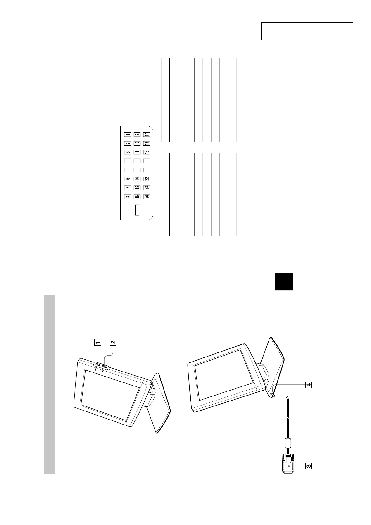
Identifying parts and controls
See the pages in parentheses for further details.
Right
Left
(Continued)
8
1 1 Power switch and indicator (pages 10, 12)
This switch turns the display on and off.
The indicator lights up in green when the display is turned on.
The indicator lights up in orange when the display is in power saving
mode.
2 2 +/– Brightness control
This control adjusts the brightness of the screen.
3 DVI video input connector (page 9)
This connector inputs digital RGB video signals.
Pin No. Signal
1 TMDS Data 2–
2 TDMS Data 2+
3 TDMS Data 2 Shield
6 DDC Clock
7 DDC Data
9 TDMS Data 1–
10 TDMS Data 1+
11 TDMS Data 1 Shield
Pin No. Signal
14 +5V Power
15 Ground (for +5V)
16 Hot Plug Detect
17 TDMS Data 0
–
18 TDMS Data 0+
19 TDMS Data 0 Shield
22 TDMS Clock Shield
23 TDMS Clock+
24 TDMS Clock–
4 DC IN connector (page 10)
This connector provides DC power to the display. Connect the AC adapter
to this connector.
OVERVIEW
This section is extracted from
instruction manual (4-649-778-01).
Confidential
1-1 PCVA-15XD2 (UC)
(END)
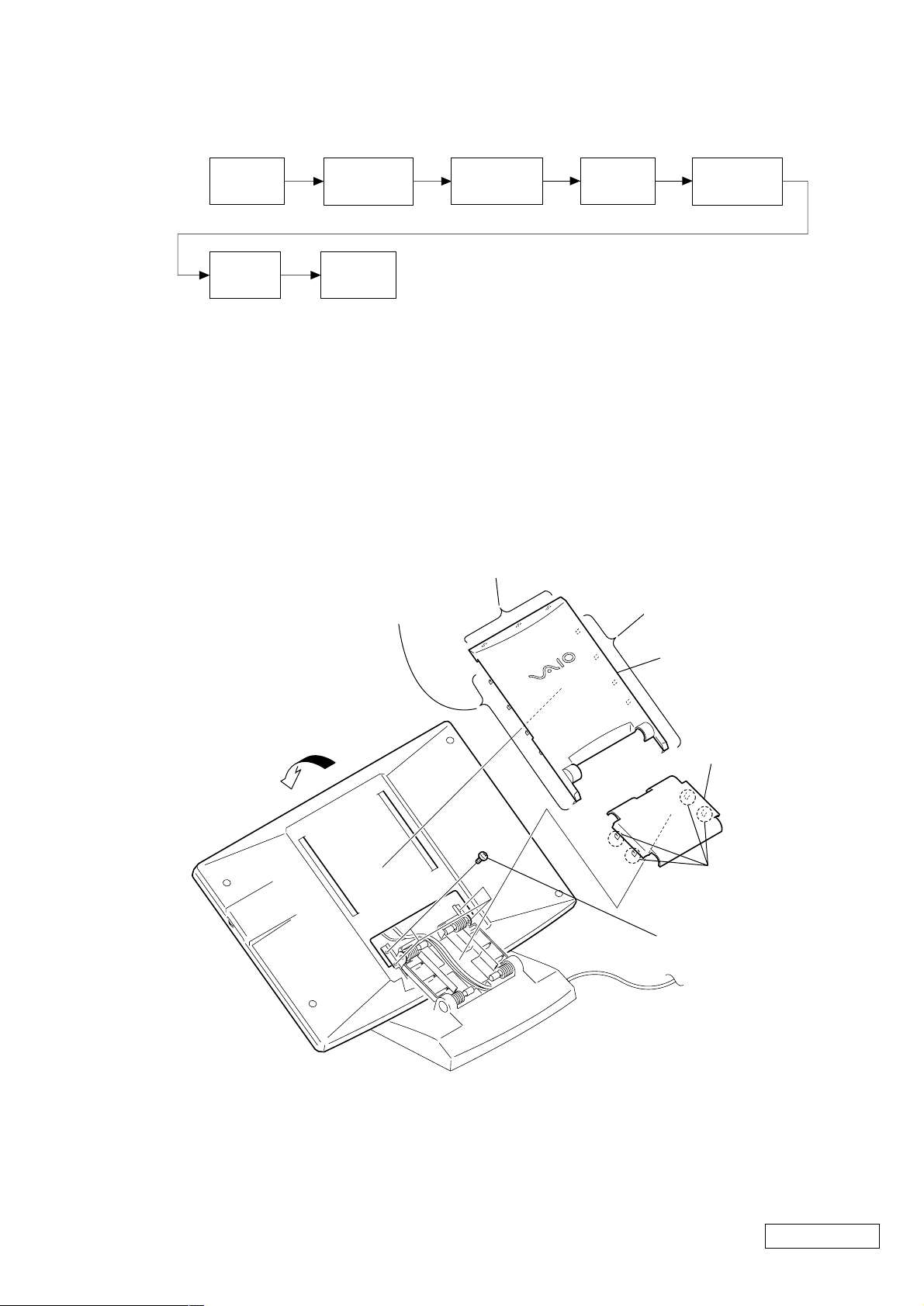
2-1. FLOWCHART
)
SECTION 2
DISASSEMBLY
ARM REAR
COVER
P2-1
LEX-23
BOARD
P2-4
• P X-X means pages that appears in this manual.
2-2. ARM REAR COVER
ARM FRONT
COVER
P2-2
IFX-105
BOARD
P2-5
4 Five claws
REAR COVER
P2-3
4 Three claws
INVERTER
UNIT
P2-3
LCD ASS'Y (S)
P2-4
4 Five claws
1 Slant the LCD ass'y (S)
in the direction of arrow A.
A
5 VAIO rear cover
3 Arm rear cover
2 Four claws
6 Four screws +PS (3 × 5
Confidential
2-1 PCVA-15XD2 (UC)

2-3. ARM FRONT COVER
Base cover upper
7
Tie band
DVI cable, Power cable
8 Remove the DVI cable and the power cable from the tie band.
6 Seven screws +BVTP (3 × 8)
q; Pull out the DVI cable and give the DVI cable a play.
5 Arm front cover
3 Raise the arm plate ass'y.
4 Four claws
2 Base cover lower
9 Pull out the power cable.
1 Seven claws
Confidential
PCVA-15XD2 (UC)
2-2

2-4. REAR COVER, INVERTER UNIT
y
1 Four screw covers
2 Four screws +B (3 × 16)
4 Rear cover
qa Inverter cable (2P)
q; Harness (LCD 2P)
3 Ten claws (Front cover ass'y)
5 Three screws +P (3 × 3)
6 Shield cover INV
7 Three screws +P (3 × 4)
9 Harness (LCD 2P)
8 Cover ass'
qs Inverter unit
Confidential
2-3 PCVA-15XD2 (UC)

2-5. LCD ASS’Y (S), LEX-23 BOARD
2 LCD cable (A)
1 Front cover ass'y
4 LCD ass'y (S)
Plastic tape
6 VR-SW cable (6P)
3 LCD cable (B)
5 Two screws +P (2 × 3)
7 LEX-23 board
Confidential
PCVA-15XD2 (UC)
2-4

2-6. IFX-105 BOARD
)
d
3 Shield cover IFX
1 Four screws +P (3 × 3)
7 Four screws +P (3 × 3)
9 IFX-105 board
8 DVI cable (2P)
4 Inverter cable (2P)
2 T wo claws
2-7. MAIN ELECTRICAL PARTS LOCATION DIAGRAM
5 VR-SW cable (6P)
6 Power cable (17P
IFX-105 board
LCD ass'y (S)
Inverter unit
LEX-23 boar
Confidential
2-5 PCVA-15XD2 (UC)
(END)

3-1. SERVICE T OOLS
SECTION 3
SERVICE OVERVIEW
Ref. No.
Name
Parts code
Application
Outside drawing
EDID writing tool
Used to connect the DVI cable and the PC during EDID
writing of the PCVA-15XD2.
1
J-2500-446-1
3-2. PROCEDURE FOR WRITING EDID DATA
1. Required tools
• EDID writing tool
• PC
• Serial cable (cross cable: D-sub pin-9 female ⇔ D-sub pin-9 female)
• EDID writing software disk
Before starting writing, copy the writing software program
(EDIDUPD) and the data file (XXXXXXX.bin) to the bootable
floppy disk already containing the system file.
• Power supply (for writing tool: + 5 V)
2
Firmware writing cable
J-2500-447-1
Used to connect the pin-7 connector (CN2) on the
IFX-105 mounted board during firmware writing of
the PCVA-15XD2.
11. Press the [ESC] key twice and press the [Q] key to terminate
writing.
12. After the MS-DOS prompt appears, disconnect the power
supply from the writing tool.
13. Disconnect the DVI cable of the display from the DVI connector
of the writing tool.
14. Disconnect the serial cable.
15. Turn off the power of the PC.
3-3. PROCEDURE FOR WRITING FIRMWARE
1. Required tools
2. Procedure
1. Connect the serial cable to the serial connector of the EDID
writing tool and the serial port COM1 of the PC.
2. Connect the DVI cable of the display to the DVI connector of
the writing tool.
3. Supply power to the writing tool.
4. Insert the writing software disk into the floppy drive.
5. Start up the PC from the floppy disk.
6. After the MS-DOS prompt appears, input the newest EDID
data file name shown below.
A:\>EDIDUPD/d:XXXXXXX.bin [enter]
7. After the writing software starts up, press the [w] key.
8. The prompt “Do you want to transfer? (y=space)” appears.
9. Press the [Space] key to start writing.
Transferring...
+>>>>------------+ } ← The above indicates the progress.
10. When writing ends normally, “Verifying...” appears for a
moment, then “Transferring succeeded. (y=continue)” appears.
• PC
• Cable for firmware writing
• Firmware writing software disk
Before starting writing, copy the writing software program
(F51PBSLAA) and the firmware file (XXXXXXX.bin) to the
bootable floppy disk already containing the system file.
2. Procedure
1. Remove the rear cover from the display.
2. Connect the cable for writing to the serial port COM1 of the
PC.
3. Connect the cable for writing to the pin-7 connector (CN2) on
the IFX board.
4. Insert the writing software disk into the floppy drive.
5. Start up the PC from the floppy disk.
6. After the MS-DOS prompt appears, input A:\>F51PBSLA
[enter].
Confidential
3-1
PCVA-15XD2 (UC)

7. After the menu of the firmware writing software appears,
connect the AC adapter to DC IN of the display and press the
Power switch.
∗ The display does not change and the power LED does not
light after the above operation.
--------------------------------------------------------------------------FlashFlex51 Boot-Strap Loader
SST Embedded Controller Applications Group
Ver.1.1, 1999.10.20
SECURITY : UNKNOW ! !
CHIP TYPE : NOT SET ! !, COM PORT : 1, BAUD RATE : bps
STATUS : SELECT CHIP TYPE AND COM PORT FIRST !
MENU SELECTIONs
0, Press 0 to EXIT to DOS
1, Press 1 to SELECT CHIP TYPE & COM PORT
2, Press 2 to DOWNLOAD BINRY FILE TO PRIMARY BLOCK
3, Press 3 to READ DATA IN PRIMARY BLOCK & SAVE AS A BINAY FILE
4, Press 4 to BLANK CHECK
5, Press 5 to SECTOR ERASE
6, Press 6 to LOCK CHIP
Enter Choice ( 0 to 6 ) : _
---------------------------------------------------------------------------
8. Input 1 (“SELECT CHIP TYPE & COM PORT”) in Enter
Choice.
9. After “Please enter SST MCU chip type (54, 58 or 59):”
appears, input 58 [enter].
10. After “Please enter COM PORT It is displayed with (1 for
COM1 OR 2 for COM2):” appears, input 1 [enter].
11. “Please enter Baud Rate: 0 for AUTO DEFECT. 1 for 38.4k, 2
for 19.2k, 3 for 9.6k, 4 for 4.8k, 5 for 2.4k, 6 for 1.2k, 7 for 600
or 8 for It is displayed with 300:” appears, input 0 [enter].
12. When the communication is established normally,
“Testing 38.4k bps on COM1 port...PASS...” appears and
“CHIP TYPE: SST89x58, COM POR T: 1, B A UD RA TE: 38.4k
bps” appears on the top of the menu.
13. Input 2 (“DOWNLOAD BINARY FILE TO PRIMARY
BLOCK”) in Enter Choice.
14. After “Input full name of f ile (.bin or Intel hex):” appears, input
the newest firmware name XXXXXXX.bin [enter].
-------------------------------------
Wait for two or three minutes.
-------------------------------------
15. After writing ends normally, “ST A TUS: VERIFY OK!” appears
on the top of the menu.
16. Input 0 (“EXIT to DOS”) in Enter Choice.
17. After the MS-DOS prompt appears, disconnect the A C adapter
from the display.
∗ The power cannot be turned off by using the Power switch.
18. Disconnect the cable for writing.
19. Turn off the power of the PC.
Confidential
3-2PCVA-15XD2 (UC)
(END)

4-1. SYSTEM CONFIGURATION
SECTION 4
BLOCK DIAGRAM
LCD Panel
LCD
LCD
Cable
45
30
Cable
(B)
(A)
2
Inverter
2
IFX-105 Board
Main Unit of LCD Display
Power Cord (2P)
Inverter Cable
7
AC Adaptor
VR_SW
Power
6
2
Cable
Cable
DVI
LEX-23
Board
Cable
4-2. BLOCK DIAGRAM
DC12V
DVI I/F
TMDS
EDID Data
5V
EEPROM
512byte
(for Debug)
Serial I/F
SiI141
Serial
12V
VSYNC,HSYNC,
DE,ODCK,SCDT
3.3V
QE0-23
RxD,TxD
DC/DC Converter
Sage
CHEETAH4
Microcontroller
with FlashROM
12V
PENVDD
5V
VSYNC,HSYNC,DE,DCLK
R/G/B
PENBKL
5V
LED
PowerSW
5V
FET
VR
LCD
Inverter
VR_SW
Socket
for
Optional ROM
Confidential
4-1 PCVA-15XD2 (UC)
(END)

SECTION 5
FRAME HARNESS
5-1. CONNECTOR LIST
1. IFX-105 BOARD
CN1
pin assignments :
Pin Signal Name
1VR
2 VR (GND)
3 CTRL
4 GND
5 GND
6VIN
7VIN
CN2
pin assignments :
Pin Signal Name
1 RXD
2 TXD
3 GND
4 GND
5 GND
6 DL_JP
7 DL_PW
CN4
pin assignments :
Pin Signal Name
1 +5V
2 BLVR
3 PWR_SW
4 GND
5 SUS_LED
6 PW_LED
CN6
pin assignments :
Pin Signal Name
1 +12V
2 NO PIN
3 GND
CN10
pin assignments:
Pin Signal Name Pin Signal Name
1 TEST 24 GO7
2 TEST 25 GND
3 TEST 26 BO0
4 VCC 27 BO1
5 VCC 28 BO2
6 RO0 29 BO3
7 RO1 30 GND
8 RO2 31 BO4
9 RO3 32 BO5
10 GND 33 BO6
11 RO4 34 BO7
12 RO5 35 GND
13 RO6 36 NC
14 RO7 37 GND
15 GND 38 HD
16 GO0 39 GND
17 GO1 40 VD
18 GO2 41 GND
19 GO3 42 DENA
20 GND 43 GND
21 GO4 44 DCLK
22 GO5 45 GND
23 GO6
CN11
pin assignments:
Pin Signal Name Pin Signal Name
1 RE0 16 GE4
2 RE1 17 GE5
3 RE2 18 GE6
4 RE3 19 GE7
5 GND 20 GND
6 RE4 21 BE0
7 RE5 22 BE1
8 RE6 23 BE2
9 RE7 24 BE3
10 GND 25 GND
11 GE0 26 BE4
12 GE1 27 BE5
13 GE2 28 BE6
14 GE3 29 BE7
15 GND 30 GND
CN9
pin assignments:
Pin Signal Name Pin Signal Name
1 RXC SHIELD 11 NC
2 RXC+ 12 RX1–
3 DDC GND 13 RX1 SHIELD
4 RXC– 14 RX1+
5 DDC+5V 15 DDC/SCL
6NC16NC
7 RX0 SHIELD 17 DDC/SDA
8 RX0– 18 RX2–
9 SENSE 19 RX2 SHIELD
10 RX0+ 20 RX2+
2. LEX-23 BOARD
CN101
pin assignments :
Pin Signal Name
1 PW_LED
2 SUS_LED
3 GND
4 PWR_SW
5 BLVR
6 +5V
Confidential
5-1 PCVA-15XD2 (UC)

5-2. FRAME HARNESS DIAGRAM
IFX-105 BOARD
LCD PANEL
1
CN11
1
CN10
CN6
CN9
1
CN4
CN1
1
1
CN101
LEX-23 BOARD
1
DC-IN
DVI CABLE
1
CN2
CN1
1
1
1
CN-IN2 CN-IN1
INVERTER UNIT
CN3
1
Confidential
PCVA-15XD2 (UC)
5-2
(END)

SECTION 6
EXPLODED VIEW
NOTE:
• -XX, -X mean standardized parts, so they may have some differences
from the original one.
• Items marked “S” in the S/P column are normally required for routine
service work. Items marked “O” are not stocked since they are seldom
required for routine service. Some delay should be anticipated when
ordering these items.
6-1. EXPLODED VIEW AND PARTS LIST
1
37
2
3
not supplied
38
The components identified by mark ! or
dotted line with mark ! are critical for safety.
Replace only with part number specified.
Les composants identifiés par une marque
! sont critiques pour la sécurité.
Ne les remplacer que par une pièce portant
le numéro spécifié.
a
b
c
18
19
21
20
6-2. PARTS LIST (ACCESSORIES AND PACKING
MATERIALS)
S/P Ref.No. Part No. Description S/P Ref.No. Part No. Description
S 1 X-4623-150-1 COVER ASSY, FRONT
S 2 4-045-165-11 EMBLEM (NO.6), SONY
O 3 4-647-422-01 TACT COVER
O 4 4-647-415-01 SHIELD COVER IFX
S 5 1-960-593-11 CABLE, VR-SW
S 6 7-621-255-15 SCREW +P 2X3
S 7 A-8066-021-A MOUNTED PWB LEX-23
O 8 X-4622-950-1 FRAME ASSY
S 9 7-682-645-01 SCREW +PS 3X4
O 10 4-644-445-01 CLAMP, CABLE
S 11 A-8066-022-A MOUNTED PWB IFX-105
O 12 4-647-752-01 ANCHOR, MINIATURE CODE
S 13 1-960-592-11 CABLE, INVERTER
S 14 1-476-153-11 INVERTER UNIT
O 15 X-4623-314-1 COVER ASSY
S 16 7-682-144-01 SCREW +P 3X3
O 17 4-647-416-01 SHIELD COVER INV
S 18 7-682-552-09 SCREW +B 3X16
S 19 4-644-474-01 COVER, SCREW
S 20 4-647-413-03 REAR COVER
0 S 1-476-159-12 ADAPTOR, AC
0 S 1-782-614-21 CORD, POWER
S 4-649-778-01 MANUAL, INSTRUCTION
S 21 4-647-408-11 VAIO REAR COVER
S 22 7-682-145-09 SCREW +P 3X4 (BLACK)
27
e
30
36
not supplied
not
supplied
5
9
41
6
7
33
25
26
31
d
f
g
9
41
39
not supplied
c
d
13
40
14
h
12
e
10
40
9
a
11
16
22
15
8
29
28
22
j
22
9
23
f
32
g
j
24
22
not supplied
S 23 X-4622-836-1 HINGE ASSY (L)
S 24 X-4622-835-1 HINGE ASSY (R)
S 25 4-647-410-01 BASE COVER LOWER
S 26 4-647-409-02 BASE COVER UPPER
S 27 4-647-406-01 ARM REAR COVER
S 28 1-960-590-11 CABLE, DVI
S 29 1-960-591-11 CABLE, POWER
S 30 1-960-611-11 CABLE, LCD (B)
S 31 X-4622-837-2 PLATE ASSY, ARM
S 32 X-4622-842-1 PLATE, BASE
S 33 4-647-405-01 ARM FRONT COVER
S 34 4-649-451-01 FOOT, RUBBER
S 35 7-685-646-79 SCREW +BVTP 3X8 TYPE2 IT-3
S 36 1-960-610-11 CABLE, LCD (A)
S 37 4-642-125-01 LABEL, ENERGY STAR
S 38 A-8047-289-A LCD (ADI/15XGA) ASSY(S)
S 39 4-651-656-01 PLATE
S 40 4-651-483-01 SPACER
S 41 7-682-646-01 SCREW +PS 3X5
16
h
4
b
16
17
34
35
Confidential
6-26-1
PCVA-15XD2 (UC)
(END)

PCVA-15XD2 (UC)
9-928-380-11
Sony Corporation
Information T echnology Company
— 24 —
This manual and the constituent data may not be
replicated, copied nor reprinted in whole or in part
without prior written authorization of Sony Corporation.
English
2000J16DOC-1
© 2000 Sony Corporation
Published by PNC Planning & Control Dept. [SKZ]
 Loading...