

Page 1
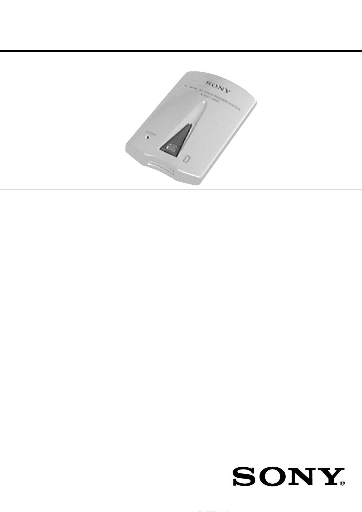
MSGC-US10
SERVICE MANUAL
Ver 1.0 2001. 01
Ver 1.0 2001. 07
SPECIFICATIONS
MG Memory Stick Reader/Writer
Interface: USB interface
Operating voltage 5 V DC (supplied from USB cable)
Current consumption Action Max. 100 mA
External dimensions Approx. 68 × 20 × 108 mm (w/h/d)
Mass Approx. 65 g
Operating environment 0 °C to 40 °C (condensation not allowed)
Standby Max. 500 µA
AEP Model
Hong Kong Model
Design and specifications are subject to change
without notice.
MAGICGATE MEMORY STICK
READER/WRITER
9-873-246-01
2001G0400-1
© 2001. 7
Sony Corporation
Personal Audio Company
Shinagawa Tec Service Manual Production Group
1
Page 2

MSGC-US10
Program©2000 Sony Corporation
Documentation©2001 Sony Corporation
OpenMG and its logo are trademarks of Sony Corporation.
“MagicGate Memory Stick,” , “Memory Stick, ” , are trademarks of
Sony Corporation.
“MagicGate ” and are trademarks Sony Corporation.
IBM and PC/AT are registered trademarks of International Business
Machines Corporation.
Microsoft, Windows, Windows NT and Windows Media are trademarks or
registered trademarks of Microsoft Corporation in the United States and/or
other countries.
Copyright©1995 Microsoft Corporation. All Right Reserved.
Portion Copyright©1995 Microsoft Corporation.
MMX and Pentium are registered trademarks or trademarks of Intel
Corporation.
All other trademarks and registered trademarks are trademarks or registered
trademarks of their respective holders.
TABLE OF CONTENTS
1. GENERAL
Before You Begin ................................................................. 3
Basic Operations .................................................................. 6
Enjoying Digital Music with OpenMG™ Jukebox ............. 6
Other information................................................................. 8
2. DISASSEMBLY
2-1. Case (Lower) ...................................................................... 10
3. DIAGRAMS....................................................................... 11
3-1. Printed Wiring Board –Main Section– ............................... 12
3-2. Schematic Diagram –Main Section–.................................. 13
4. EXPLODED VIEW
4-1. Main Section ...................................................................... 15
5. ELECTRICAL PARTS LIST ........................................ 16
Notes on chip component replacement
• Never reuse a disconnected chip component.
• Notice that the minus side of a tantalum capacitor may be
damaged by heat.
SAFETY-RELATED COMPONENT WARNING!!
COMPONENTS IDENTIFIED BY MARK 0 OR DOTTED LINE
WITH MARK 0 ON THE SCHEMATIC DIAGRAMS AND IN
THE PARTS LIST ARE CRITICAL TO SAFE OPERATION.
REPLACE THESE COMPONENTS WITH SONY P ARTS WHOSE
PART NUMBERS APPEAR AS SHOWN IN THIS MANUAL OR
IN SUPPLEMENTS PUBLISHED BY SONY.
2
Page 3
SECTION 1
GENERAL
MSGC-US10
This section is extracted from
instruction manual.
3
Page 4
MSGC-US10
4
Page 5
MSGC-US10
5
Page 6

MSGC-US10
6
Page 7

MSGC-US10
7
Page 8

MSGC-US10
8
Page 9

MSGC-US10
9
Page 10

MSGC-US10
SECTION 2
DISASSEMBLY
Note : Follow the disassembly procedure in the numerical order given.
2-1. CASE (LOWER)
claws
2 P 2x6
3
1 P 2x6
4 case (lower)
10
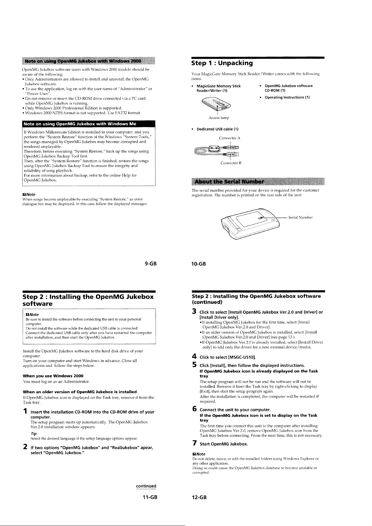
Page 11

SECTION 3
p
p
DIAGRAMS
MSGC-US10
THIS NOTE IS COMMON FOR PRINTED WIRING
BOARD AND SCHEMATIC DIAGRAM.
(In addition to this, the necessary note is
printed in each block.)
for schematic diagram:
• All capacitors are in µF unless otherwise noted. pF: µµF
50 WV or less are not indicated except for electrolytics
and tantalums.
• All resistors are in Ω and 1/
specified.
• % : indicates tolerance.
f
•
• C : panel designation.
• A : B+ Line.
• Power voltage is dc 5V and fed with regulated dc power
• Voltages are taken with a VOM (Input impedance 10 MΩ).
• Voltage and waveforms are dc with respect to ground
• Waveforms are taken with a oscilloscope.
• Circled numbers refer to waveforms.
for printed wiring boards:
• X : parts extracted from the component side.
• : Pattern from the side which enables seeing.
Caution:
Pattern face side: Parts on the pattern face side seen from the
(Side B) pattern face are indicated.
Parts face side: Parts on the parts face side seen from the
(Side A) parts face are indicated.
: internal component.
supply from USB connector (CN102).
Voltage variations may be noted due to normal produc-
tion tolerances.
under no-signal conditions.
no mark : Standby
Voltage variations may be noted due to normal production tolerances.
(The other layer’s patterns are not indicated.)
4
W or less unless otherwise
• Waveforms
1V AC/div, 20nsec/div
1
20 MHz
IC101
1V AC/div, 20nsec/div
2
IC101
1V AC/div, 20nsec/div
3
20 MHz
IC106
rs
48 MHz
th
6
(SCK0)
(X0)
(XT)
1.85 Vp-
1.65 Vp-p
1.85 Vp-
• Semiconductor
Location
Ref. No. Location
D001 I-13
D002 B-5
IC101 C-4
IC102 C-6
IC103 E-2
IC104 C-2
IC105 E-6
IC106 C-3
IC107 F-6
IC108 G-6
IC109 G-6
Q101 G-2
Q102 G-2
Q104 D-3
• Main board is four-layer printed board.
However, the patterns of layers 2 and 3 have not been included in this diagrams.
Replacement of IC107 on main board
*
requires a special tool.
• Lead Layouts
Lead layout of conventional IC
CSP (chip size package)
surface
11 11
Page 12

MSGC-US10
3-1. PRINTED WIRING BOARD — MAIN SECTION — • Refer to page 11 for Note. Refer to page 11 for Semiconductor Locations.
A
B
C
D
E
1
234567891011121314
CN102
MAIN BOARD (SIDE B)
TP001
C109
C110
C121
1
32
IC104
C105
C106
TP002
C122
IC103
TP003
21
3
C107
C108
L104
C137
L103
C119
C120
R119
L102
4
6
L107
C117
TP007
IC106
X102
3
1
R164
R155
Q104
SDG
R123
R154
R162
C138
R156
R161
10
R165
15
20
R163
25
30
32
TP005
PS101
C118
1
5
L105
125128
3335 40
R113
R112
R110
R111
R140
R101
R104
C126
FB102
IC101
R105
TP008
R107
X101
100105110115120
R114
FB101
C129
97
6455 6045 50
R106
L106
R147
R153
R144
R143
D002
R139
R137
R135
R133
96
R131
R129
90
R127
85
R125
80
C128
75
70
C127
65
R151
R150
R149
R118
C123
R136
R134
R117
R138
R132
R130
R128
R126
R124
R145
3
4
R166
1
5
TP009
IC105
R146
152024
C134
IC102
C115
510
4540353025
L101
1
46
C116
MAIN BOARD (SIDE A)
142
3
F
G
H
Q102
ECB
C102
C103
R108
C104
R109
Q101
BCE
C101
R141
15
CN101
TP006
10
IC107
*
C132
C133
C131
IC108
R158
5
1
R157
4
3
TP004
R120
C130
C136
D001
ACCESS
C135
5
1
IC109
4
3
I
J
1-679-144-
13
(13)
1-679-144-
1212
13
(13)
Page 13

3-2. SCHEMATIC DIAGRAM — MAIN SECTION — • Refer to page 11 for Note and Waveforms. Refer to page 14 for IC Block Diagram.
MEMORY STICK
)
(
CONNECTOR
MSGC-US10
13 13
IC B/D
Page 14

MSGC-US10
• IC BLOCK DIAGRAM
IC108 TC7SH32FU
INB
VCC OUT Y
5 4
1 2 3
INA GND
MEMO
1414
Page 15

NOTE:
• The mechanical parts with no reference
number in the exploded views are not supplied.
• Items marked “*” are not stocked since
they are seldom required for routine service.
Some delay should be anticipated
when ordering these items.
4-1. MAIN SECTION
not supplied
SECTION 4
EXPLODED VIEW
• -XX and -X mean standardized parts, so
they may have some difference from the
original one.
• Color Indication of Appearance Parts
Example :
KNOB, BALANCE (WHITE) ... (RED)
R
Parts Color Cabinet’s Color
• Accessories and packing materials are
given in the last of this parts list.
MSGC-US10
R
CN102
1
CN101
2
3
3
4
Ref. No. Part No. Description Remark
* 1 A-3323-662-A MAIN BOARD, COMPLETE
2 3-220-912-01 CASE (LOWER)
3 7-685-104-14 SCREW +P 2X6 TYPE2 NON-SLIT
Ref. No. Part No. Description Remark
4 3-226-838-01 FOOT, RUBBER
CN101 1-793-111-21 CONNECTOR, MEMORY STICK
* CN102 1-784-010-11 CONNECTOR, USB (B)
15
Page 16

MSGC-US10
SECTION 4
MAIN
NOTE:
• Due to standardization, replacements in
the parts list may be different from the
parts specified in the diagrams or the
components used on the set.
• -XX and -X mean standardized parts, so
they may have some difference from the
original one.
• RESISTORS
All resistors are in ohms.
METAL:Metal-film resistor.
METAL OXIDE: Metal oxide-film resistor.
F:nonflammable
Ref. No. Part No. Description Remark Ref. No. Part No. Description Remark
* A-3323-662-A MAIN BOARD, COMPLETE
*********************
< CAPACITOR >
ELECTRICAL PARTS LIST
• CAPACITORS
uF : µF
• COILS
uH : µH
• Items marked “*” are not stocked since
they are seldom required for routine service.
Some delay should be anticipated
when ordering these items.
• SEMICONDUCTORS
In each case, u : µ, for example:
uA.. : µA.. uPA.. : µPA..
uPB.. : µPB.. uPC.. : µPC.. uPD.. : µPD..
FB101 1-469-083-21 INDUCTOR, FERRITE BEAD 600uH
FB102 1-469-083-21 INDUCTOR, FERRITE BEAD 600uH
When indicating parts by reference
number, please include the board.
< FERRITE BEAD >
C101 1-107-820-11 CERAMIC CHIP 0.1uF 16V
C102 1-107-820-11 CERAMIC CHIP 0.1uF 16V
C103 1-124-779-00 ELECT CHIP 10uF 20% 16V
C104 1-124-779-00 ELECT CHIP 10uF 20% 16V
C105 1-107-820-11 CERAMIC CHIP 0.1uF 16V
C106 1-124-779-00 ELECT CHIP 10uF 20% 16V
C107 1-107-820-11 CERAMIC CHIP 0.1uF 16V
C108 1-124-779-00 ELECT CHIP 10uF 20% 16V
C109 1-107-820-11 CERAMIC CHIP 0.1uF 16V
C110 1-124-779-00 ELECT CHIP 10uF 20% 16V
C115 1-124-779-00 ELECT CHIP 10uF 20% 16V
C116 1-107-820-11 CERAMIC CHIP 0.1uF 16V
C117 1-124-779-00 ELECT CHIP 10uF 20% 16V
C118 1-107-820-11 CERAMIC CHIP 0.1uF 16V
C119 1-124-779-00 ELECT CHIP 10uF 20% 16V
C120 1-107-820-11 CERAMIC CHIP 0.1uF 16V
C121 1-107-820-11 CERAMIC CHIP 0.1uF 16V
C122 1-107-820-11 CERAMIC CHIP 0.1uF 16V
C123 1-164-939-11 CERAMIC CHIP 0.0022uF 10% 16V
C126 1-107-820-11 CERAMIC CHIP 0.1uF 16V
C127 1-107-820-11 CERAMIC CHIP 0.1uF 16V
C128 1-107-820-11 CERAMIC CHIP 0.1uF 16V
C129 1-107-820-11 CERAMIC CHIP 0.1uF 16V
C130 1-107-820-11 CERAMIC CHIP 0.1uF 16V
C131 1-107-820-11 CERAMIC CHIP 0.1uF 16V
< IC >
IC101 8-759-695-24 IC F731791CPBK-TEB
IC102 X-3380-692-1 IC ROM (MBM29LV200BC-90PFTN-MG3)
IC103 8-759-829-80 IC XC62FP1802MR
IC104 8-759-486-73 IC XC62FP3302PR
IC105 8-759-593-23 IC S-80928ANMP-DDR-T2
IC106 8-759-486-57 IC XC2141C21AMR
@ IC107 8-752-399-04 IC CXD3450GG
IC108 8-759-196-97 IC TC7SH32FU-TE85R
IC109 8-759-196-97 IC TC7SH32FU-TE85R
< COIL >
L101 1-410-381-11 INDUCTOR CHIP 10uH
L102 1-410-381-11 INDUCTOR CHIP 10uH
L103 1-410-381-11 INDUCTOR CHIP 10uH
L104 1-469-324-21 FERRITE, EMI (SMD)
L105 1-414-226-21 FERRITE, EMI (SMD)
L106 1-414-226-21 FERRITE, EMI (SMD)
L107 1-469-324-21 FERRITE, EMI (SMD)
< IC LINK >
PS101 1-533-606-21 LINK, IC (500mA)
< TRANSISTOR >
C132 1-107-820-11 CERAMIC CHIP 0.1uF 16V
C133 1-107-820-11 CERAMIC CHIP 0.1uF 16V
C134 1-107-820-11 CERAMIC CHIP 0.1uF 16V
C135 1-107-820-11 CERAMIC CHIP 0.1uF 16V
C136 1-124-779-00 ELECT CHIP 10uF 20% 16V
C137 1-234-494-21 FILTER, EMI REMOVAL (SMD)
C138 1-164-850-11 CERAMIC CHIP 10PF 0.5PF 16V
< CONNECTOR >
CN101 1-793-111-21 CONNECTOR, MEMORY STICK
* CN102 1-784-010-11 CONNECTOR, USB (B) (USB CONNECTOR)
< DIODE >
D001 8-719-082-95 LED TLO220 (ACCESS)
D002 8-719-078-01 DIODE NNCD6.8LG-T1
16
Q101 8-729-051-23 TRANSISTOR 2SA2018TL
Q102 8-729-907-00 TRANSISTOR DTC114EU
Q104 8-729-032-62 FET 2SJ347-TE85L
< RESISTOR >
R101 1-218-939-11 RES-CHIP 68 5% 1/16W
R104 1-218-977-11 RES-CHIP 100K 5% 1/16W
R105 1-218-977-11 RES-CHIP 100K 5% 1/16W
R106 1-218-977-11 RES-CHIP 100K 5% 1/16W
R107 1-218-981-11 RES-CHIP 220K 5% 1/16W
R108 1-218-955-11 RES-CHIP 1.5K 5% 1/16W
R109 1-218-977-11 RES-CHIP 100K 5% 1/16W
R110 1-218-981-11 RES-CHIP 220K 5% 1/16W
R111 1-218-981-11 RES-CHIP 220K 5% 1/16W
R112 1-208-643-11 RES-CHIP 22 5% 1/16W
@Replacement of CXD3450GG (IC107) used in this
set requires a special tool.
Therefore, it cannot be replaced.
Page 17

MSGC-US10
MAIN
Ref. No. Part No. Description Remark Ref. No. Part No. Description Remark
R113 1-208-643-11 RES-CHIP 22 5% 1/16W
R114 1-218-989-11 RES-CHIP 1M 5% 1/16W
R117 1-218-977-11 RES-CHIP 100K 5% 1/16W
R118 1-218-981-11 RES-CHIP 220K 5% 1/16W
R119 1-218-981-11 RES-CHIP 220K 5% 1/16W
R120 1-218-981-11 RES-CHIP 220K 5% 1/16W
R123 1-218-955-11 RES-CHIP 1.5K 5% 1/16W
R124 1-218-981-11 RES-CHIP 220K 5% 1/16W
R125 1-218-981-11 RES-CHIP 220K 5% 1/16W
R126 1-218-981-11 RES-CHIP 220K 5% 1/16W
R127 1-218-981-11 RES-CHIP 220K 5% 1/16W
R128 1-218-981-11 RES-CHIP 220K 5% 1/16W
R129 1-218-981-11 RES-CHIP 220K 5% 1/16W
R130 1-218-981-11 RES-CHIP 220K 5% 1/16W
R131 1-218-981-11 RES-CHIP 220K 5% 1/16W
R132 1-218-981-11 RES-CHIP 220K 5% 1/16W
R133 1-218-981-11 RES-CHIP 220K 5% 1/16W
R134 1-218-981-11 RES-CHIP 220K 5% 1/16W
R135 1-218-981-11 RES-CHIP 220K 5% 1/16W
R136 1-218-981-11 RES-CHIP 220K 5% 1/16W
ACCESSORIES & PACKING MATERIALS
********************************
1-792-826-21 CORD, CONNECTION
3-228-138-31 SOFT (CD-ROM), APPLICATION
3-228-141-11 MANUAL, INSTRUCTION (ENGLISH,FRENCH,
GERMAN)
R137 1-218-981-11 RES-CHIP 220K 5% 1/16W
R138 1-218-981-11 RES-CHIP 220K 5% 1/16W
R139 1-218-981-11 RES-CHIP 220K 5% 1/16W
R140 1-218-981-11 RES-CHIP 220K 5% 1/16W
R141 1-218-945-11 RES-CHIP 220 5% 1/16W
R143 1-218-981-11 RES-CHIP 220K 5% 1/16W
R144 1-218-981-11 RES-CHIP 220K 5% 1/16W
R145 1-218-975-11 RES-CHIP 68K 5% 1/16W
R146 1-218-965-11 RES-CHIP 10K 5% 1/16W
R147 1-218-981-11 RES-CHIP 220K 5% 1/16W
R149 1-218-981-11 RES-CHIP 220K 5% 1/16W
R150 1-218-981-11 RES-CHIP 220K 5% 1/16W
R151 1-218-981-11 RES-CHIP 220K 5% 1/16W
R153 1-218-981-11 RES-CHIP 220K 5% 1/16W
R154 1-218-981-11 RES-CHIP 220K 5% 1/16W
R155 1-218-981-11 RES-CHIP 220K 5% 1/16W
R156 1-218-981-11 RES-CHIP 220K 5% 1/16W
R157 1-218-981-11 RES-CHIP 220K 5% 1/16W
R158 1-218-981-11 RES-CHIP 220K 5% 1/16W
R161 1-218-981-11 RES-CHIP 220K 5% 1/16W
R162 1-218-981-11 RES-CHIP 220K 5% 1/16W
R163 1-218-957-11 RES-CHIP 2.2K 5% 1/16W
R164 1-218-981-11 RES-CHIP 220K 5% 1/16W
R165 1-218-981-11 RES-CHIP 220K 5% 1/16W
R166 1-218-981-11 RES-CHIP 220K 5% 1/16W
< VIBRATOR >
X101 1-795-097-21 VIBRATOR, CERAMIC (48MHz)
X102 1-781-945-21 VIBRATOR, CERAMIC (20MHz)
*************************************************************
17
Page 18

MSGC-US10
REVISION HISTORY
Clicking the version allows you to jump to the revised page.
Also, clicking the version at the upper right on the revised page allows you to jump to the next revised
page.
Ver. Date Description of Revision
1.0 2001. 07 New
18
 Loading...