

Page 1
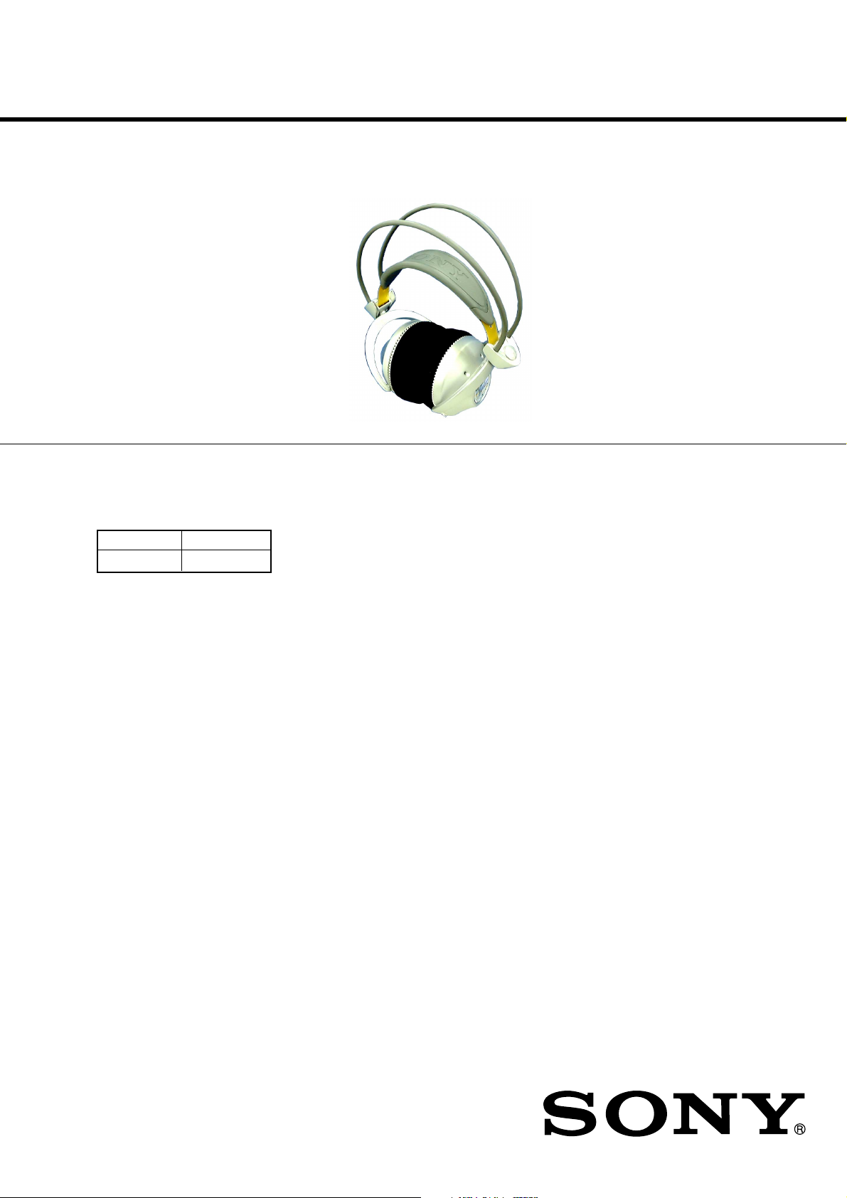
MDR-RF975R
SERVICE MANUAL
Ver 1.1 2001. 06
MDR-RF975R is the component model block one in the MDR-RF975RK.
COMPONENT MODEL NAME FOR MDR-RF975RK
Headphones MDR-RF975R
Transmitter TMR-RF975R
US Model
SPECIFICATIONS
Headphones
Power source DC 2.4 V: Built-in rechargeable
battery
Mass Approx. 350 g (12.3 oz.) incl.
built-in rechargeable battery
Built-in Ni-MH rechargeable battery
Model name NH-AAC
Voltage 1.2 V
Capacity 1,000 mAh
Design and specifications are subject to change without
notice.
9-873-141-12
2001F0200-1
© 2001.6
HEADPHONES
Sony Corporation
Personal Audio Company
Shinagawa Tec Service Manual Production Group
Page 2
MDR-RF975R
SECTION 1
GENERAL
TABLE OF CONTENTS
Specifications ............................................................................ 1
1. GENERAL ......................................................................... 2
2. DISASSEMBLY
2-1. Driver (R Side), RX-BASE Board ........................... 3
2-2. SW Board, Hanger (R) ............................................. 4
2-3. Holder (R) ................................................................. 4
2-4. Driver (L Side) .......................................................... 5
2-5. Hanger (L) ................................................................ 6
2-6. Holder (L) ................................................................. 6
3. ELECTRICAL ADJUSTMENTS
3-1. Free Run Frequency Check and Adjustments........... 7
3-2. Receive Frequency Check and Adjustments ............ 7
3-3. Carrier Modulation Check ........................................ 7
3-4. Expander Output Check ............................................ 7
3-5. Separation Check ...................................................... 7
4. DIAGRAMS
4-1. Block Diagrams .......................................................11
4-2. Schematic Diagram ................................................. 12
4-3. Printed Wiring Board .............................................. 13
5. XPLODEDVIEWS....................................................... 14
This section is extracted from
instruction manual.
5
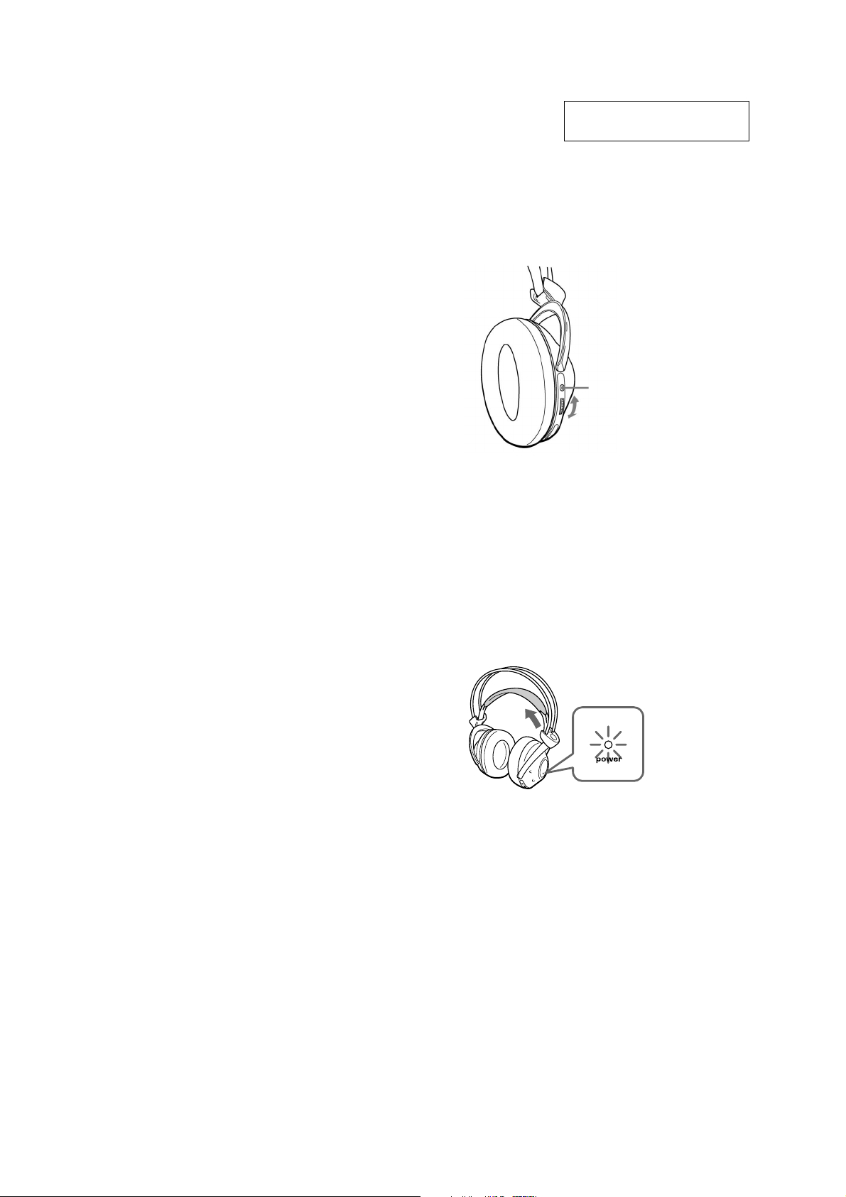
Turn up the volume to a moderate level
with the VOL control.
Press the TUNING button briefly for
automatic tuning of the headphones.
If you do not receive a clear audio signal,
press it again.
TUNING
button
VOL control
Try the above steps 3 and 5 until the
receiving performance becomes better.
6. ELECTRICAL PARTSLIST..................................... 15
Auto power on/off function
When you remove the headphones from your
head, the power turns off automatically. Do not
allow the self adjusting band to be pulled up,
otherwise the headphones will be switched on.
The power turns on.
Flexible Circuit Board Repairing
• Keep the temperature of soldering iron around 270°C
during repairing.
• Do not touch the soldering iron on the same conductor of the
circuit board (within 3 times).
• Be careful not to apply force on the conductor when soldering
or unsoldering.
Notes on chip component replacement
• Never reuse a disconnected chip component.
• Notice that the minus side of a tantalum capacitor may be
damaged by heat.
2
Page 3
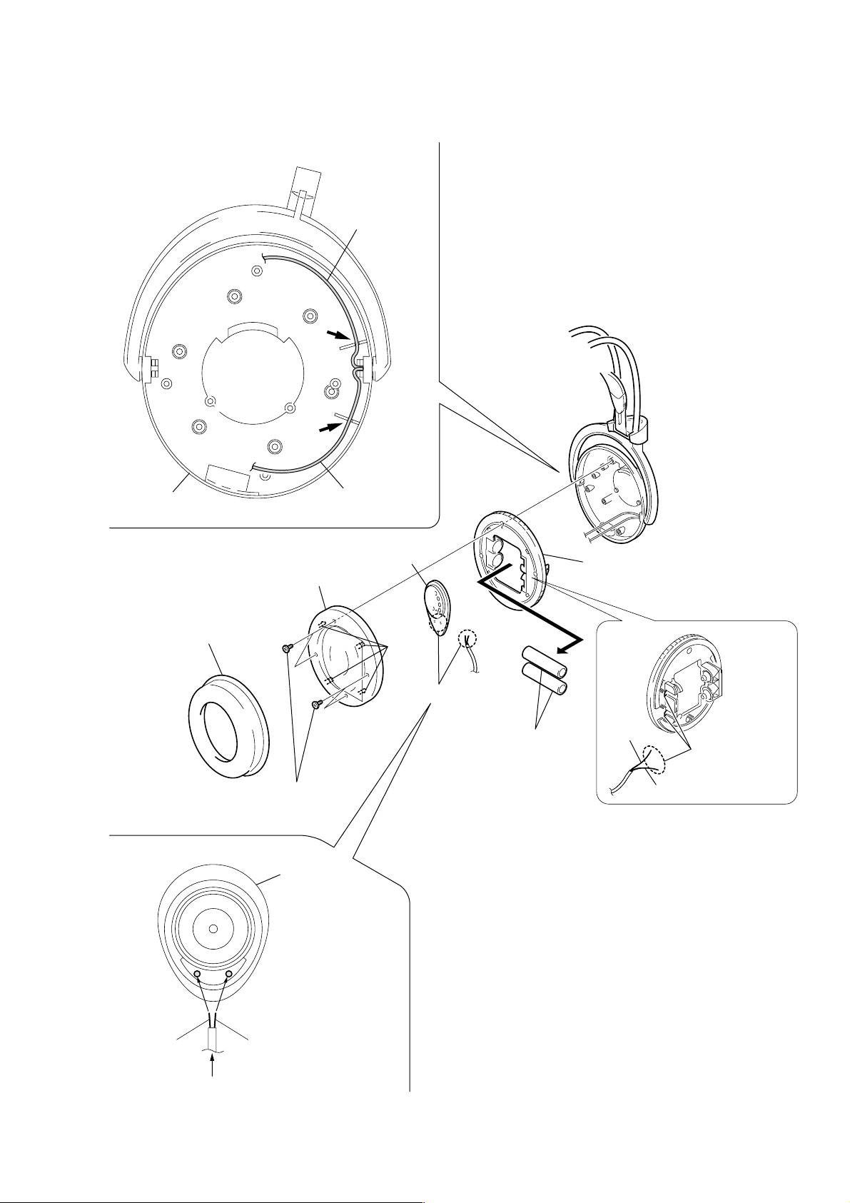
SECTION 2
DISASSEMBLY
• The equipment can be removed using the following procedure .
MDR-RF975R
Set
Driver (R side), RX-BASE board
Driver (L side), Hanger (L)
SW board, Harger (R)
Holder (L)
Note: Follow the disassembly procedure in the numerical order given .
2-1. DRIVER (R SIDE), RX-BASE BOARD
9
Volume knob
Holder (R)
Set the each leads as illustrated below.
From head
band assy (front).
From head
band assy (rear).
Groove
From
SW board.
Groove
qa
RX-BASE board
0
Remove the
eight solderings.
(Housing (R) side)
Head band
assy (front)(natural)
8
Charge terminal
7
Remove the
two solderings.
Precaution for installtion
ANT
RX-BASE board
SW board
Head band
assy (rear)(natural)
Head band
assy (rear)(green)
Driver (natural)
Driver (red)
4
Holder (R),ear pad
5
Remove the
two solderings.
6
Four
claws
Driver
2
Four screws (M 2
Housing (R)
Precaution for installtion
3
Plate (R) assy, front
1
pad, ear
× 5)
Precaution for installtion
Driver (R side)
Head band
assy (front)(red)
Solder the each leads directly to the position as shown
while being cautions of colors.
SW board
Red Natural
From RX-BASE board.
3
Page 4
MDR-RF975R
s
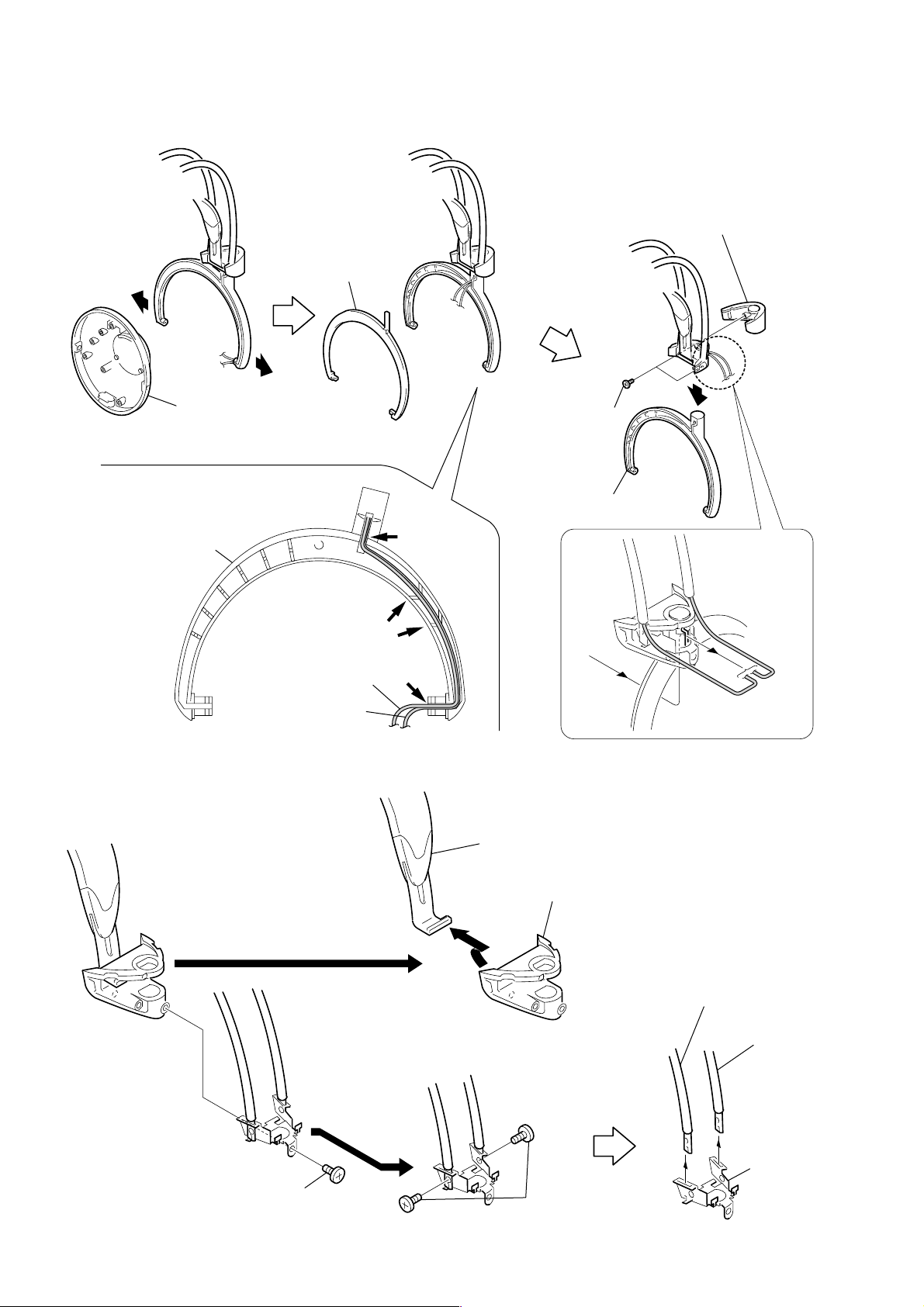
2-2. SW BOARD, HANGER (R)
1
1
2
Housing (R)
Precaution for installtion
3
Lid (R), hanger
8
7
Remove the
two solderings.
SW board
5
Holder (R)
4
Two screw
(P 2
× 8)
Set the each leads as illustrated below.
Groove
Groove
Groove
From head
band assy (front).
From head
band assy (rear).
2-3. HOLDER (R)
2
Spring
(ON/OFF)
From
SW board.
Groove
Groove
Groove
Hanger (R)
3
Holder (R)
SW board
9
6
4
Cushion assy, head
8
Band assy (front), Head
7
Band assy (rear), head
Hanger (R)
5
1
Screw (P 2
× 8)
Two screws
× 8)
(P 2
6
Chassis
4
Page 5
2-4. DRIVER (L SIDE)
Set the each leads as illustrated below.
MDR-RF975R
From head
band assy (front).
Groove
Groove
Housing (L)
Precaution for installtion
3
Plate (L) assy, front
1
Pad, ear
2
Four screws (M 2
Precaution for installtion
× 5)
Driver (L side)
From head
band assy (rear).
8
Driver
Four
claws
7
Remove the
two solderings.
4
Two "batterys,
nickle hydrogen"
6
Ear pad
holder (L)
Green
Natural
5
Remove the
two solderings.
Green Natural
From head band assy (rear).
5
Page 6
MDR-RF975R
s
2-5. HANGER (L)
1
3
Lid (L), hanger
1
2
Housing (L)
Precaution for installtion
4
Two screws
(M 2
× 5)
5
Holder (L)
Set the each leads as illustrated below.
Hanger (L)
2-6. HOLDER (L)
Groove
From head
band assy (front).
From head
band assy (rear).
Groove
Groove
7
Hanger (L)
3
Cushion assy, head
2
Holder (L)
6
6
Band assy (front),head
7
Band assy
(rear), head
5
Chassi
1
Screw (M 2
× 5)
4
Two screws
(M 1.7
× 3)
6
Page 7
SECTION 3
4
4
7
7
ELECTRICAL ADJUSTMENTS
MDR-RF975R
Ver 1.1 2001.06
Notes:
1. Use transmitter with check and adjustment alreadycompleted.
2. On adjusting the headphones section, use the transmitter as a
jig.
Headphones:MDR-RF975R
Transmitter:TMR-RF975R
Procedure:
1. Connect an oscillator with attenuator and terminator (600 Ω)
to the transmitter AUDIO IN-A connector (J402).
2. Connect an AC adapter to the transmitter DC IN 9V jack (J404).
3. Short between Q303 collector and GND on the RX board.
4. Connect DC 2.4V to the +B power line externally.
5. Connect lead wires to IC301 pin 4, pin 6, pin 7, IC 307 pin 7,
IC 308 pin 7 and GND on the RX-BASE board.
6. Connect a 33kΩ resistor between IC301 pin 4 and pin 7.
7. Connect lead wires to the speakers’ terminals (L+,L-,R+,R-)
on the RX-BASE board. (See page 9)
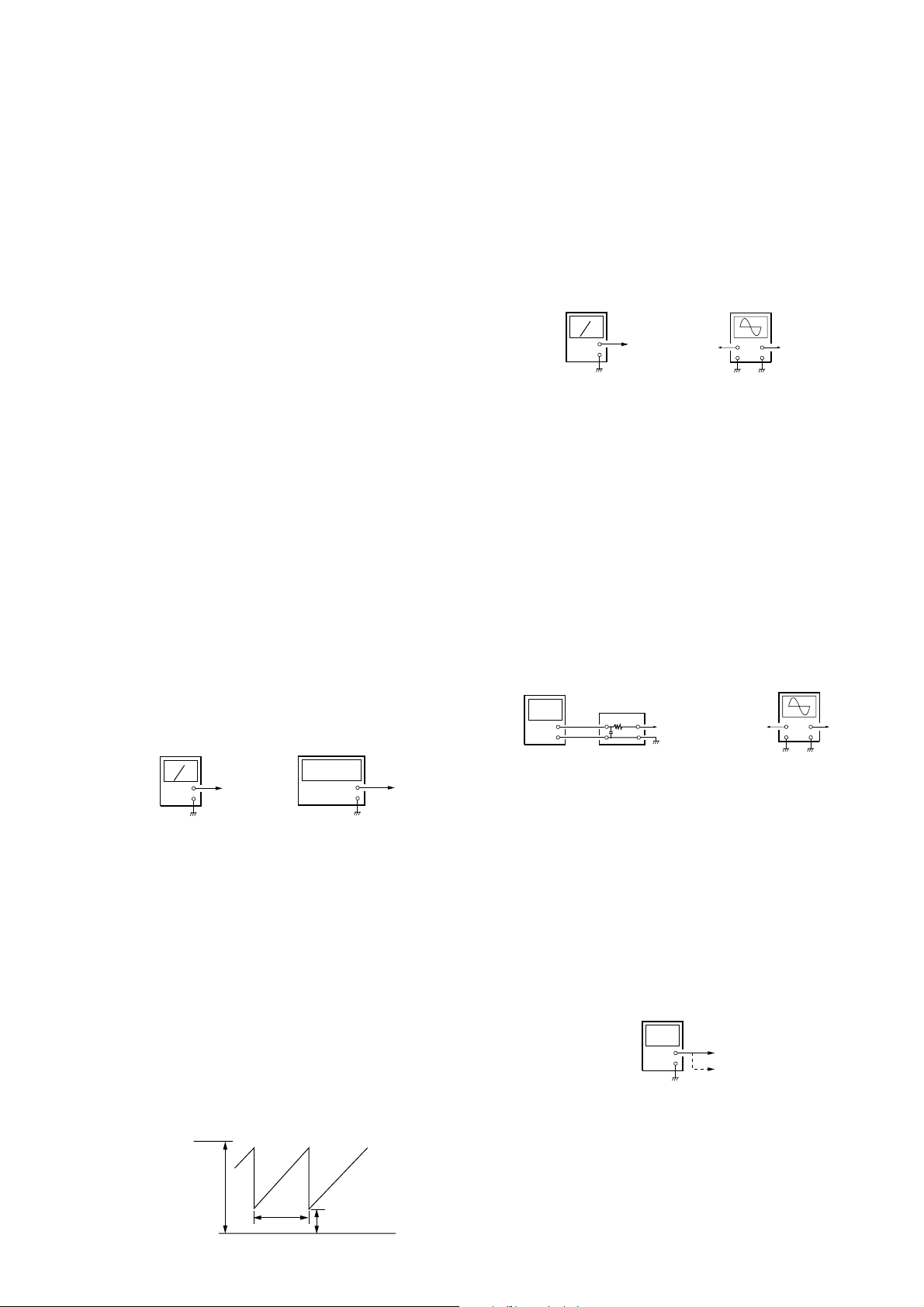
3-1. Free Run Frequency Check and Adjustment
1. Set the transmitter AUDIO IN-A connector (J402) to no signal.
Note: In this case, operation time is about 5 or 10 minutes.
Perform the confirmation for less than 5 minutes.
2. Check the transmitter power indicator (red) lights.
3. Set the transmitter CHANNEL switch to 1.
4. Connect DC 1.2V across TP and GND.
5. Connect a frequency counter to IC301 pin 4 and GND on the
RX-BASE board, then confirm the frequency within 76KHz
± 50Hz.
6. When the frequency dose not satisfy the specified value, adjust
the value of the frequency counter to specification by RV301
on the RX-BASE board.
Specified values: 76kHz ± 50Hz.
7. Remove a 33kΩ resistor between IC301 pin 4 and pin 7.
Setting :
Regulated power supply
(DC 1.2V)
TP
+
–
Frequency counter
+
–
IC301 pin
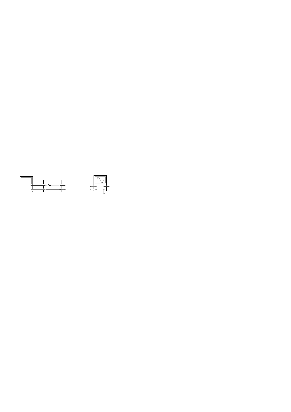
3-2. Receive Frequency Check and Adjustment
1. Set the transmitter CHANNEL switch to 2.
2. Set the transmitter NOISE FILTER switch to OFF.
3. Input a signal of 1kHz, 316mVrms to transmitter AUDIO INA(L-ch) connector only.
4. Keep distance between transmitter and headphones to 5 meters
over.
5. Set the headphones volume (RV302) to minimum.
6. Connect DC 1.2V across TP and GND.
7. Connect an oscilloscope CH1 and CH2 to IC301 pin 6 and
pin 4.
8. Check the waveform of the oscilloscope to CH1 is demodulated
1kHz signal and CH2 is GND.
9. If CH1 and CH2 are not satisfied in step 8, adjust the coil (L301)
on the RX board to satisfied step 8.
10. Open between Q303 corrector and GND on the RX board.
11. When the transmitter off, check the waveform of the
oscilloscope as follows:
1.8V
GND
2-3sec
0.6V
12. Set the transmitter CHANNEL switch to 1.
13. Push the headphones tuning switch (S301) to receive radio
frequency.
14. Check same step 8.
15. Set the transmitter CHANNEL switch to 3.
16. Push the headphones tuning switch (S301) to receive radio
frequency.
17. Check same step 8.
Setting :
Regulated power supply
(DC 1.2V)
TP
+
–
OSCILLOSCPE
IC301 pin6
CH1 CH2
+
–+–
IC301 pin
3-3. Carrier Modulation Check
1. Set the transmitter CHANNEL switch to 2.
2. Set the transmitter NOISE FILTER switch to OFF.
3. Input a signal of 1kHz, 316mVrms to transmitter AUDIO IN-A
(L-ch) connector only.
4. Set the headphones volume (RV302) to minimum.
5. Connect an oscilloscope CH1 and CH2 to IC301 pin 6 and
pin 4.
6. Push the headphones tuning switch (S301) to receive radio
frequency.
7. Check the waveform of the oscilloscope that the CH1 is
demodulated 1kHz signal and CH2 is GND.
8. Connect an AC voltmeter with LPF to IC301 pin 6 and GND.
9. Check the value of the AC voltmeter to 40mVrms ± 5mV
Setting :
Digital voltmeter
(AC range)
+
–
LPF
2.2K
33000P
IC301
pin6
OSCILLOSCPE
IC301 pin6
CH1 CH2
+
–+–
IC301 pin4
3-4. Expander Output Check
1. Set the transmitter CHANNEL switch to 2.
2. Input a signal of 1kHz, 316mVrms to transmitter AUDIO IN-A
L and R connector.
3. Connect an AC voltmeter to IC307 pin 7 and IC308 pin 7.
4. Measure the value of the AC voltmeter.
5. Input a signal of 1kHz, 31.6mVrms to transmitter AUDIO INA L and R connector.
6. Measure the value of the AC voltmeter.
7. Check the difference of the step 4 and step 6 to more than 20
dB ± 3 dB.
Setting :
Digital voltmeter
(AC range)
+
–
IC307 pin
IC308 pin
3-5. Separation Check
1. Set the transmitter CHANNEL switch to 2.
2. Set the transmitter NOISE FILTER switch to OFF.
3. Input a signal of 1kHz, 316mVrms to transmitter AUDIO IN-A
(L-ch) connector only.
4. Connect an oscilloscope CH1 to speakers terminal (L+,L-) and
CH2 to IC301 pin 4 and GND.
5. Push the headphones tuning switch (S301) receive radio
frequency.
7
Page 8
MDR-RF975R
4
Ver 1.1 2001.06
6. Check the waveform of the oscilloscope that the CH1 is
demodulated 1kHz signal and CH2 is GND.
7. Connect an AC voltmeter with LPF to speakers terminal
(L+L-).
8. Adjust the value of the AC voltmeter to specification by
headphones volume RV302.
Specified values: 155mVrms
9. Connect an AC voltmeter with LPF to speakersterminal
(R+,R-).
10. Measure the value of the AC voltmeter.
11. Check the difference of the L and R to more than 25dB.
12. Input a signal of 1kHz, 316mVrms to transmitter AUDIO IN-A
(R-ch) connector only.
13. Connect an AC voltmeter with LPF to speakers terminal
(R+,R-).
14. Adjust the value of the AC voltmeter to specification by
headphones volume RV302.
Specified values: 155mVrms
15. Connect an AC voltmeter with LPF to speakers terminal
(L+,L-).
16. Measure the value of the AC voltmeter.
17. Check the difference of the L and R to more than 25dB.
Setting :
Digital voltmeter
(AC range)
+
–
LPF
2.2K
33000P
L+ / R+
L– / R–
OSCILLOSCPE
CH1 CH2
+
L+
–+–
L–
IC301 pin
8
Page 9
)
Asjustment Location :
RX-BASE BOARD
(Conductor side)
C340
C337
R347
R349
C341
TP
GND
L301:
Receive frequency
Adjustment
R340
R346
R341
R345
S301
CF301
R342
R344
C320
R343
IC303
C316
C344
R312
D301
L301
C322
C332
C336
C315
C313
D304
power
C321
C309
R325
R308
L302
C314
C355
C312
C329
C331
C317
C319
JC335
D310
C394
C308
C306
IC301
C359
C393
C303
C307
R309
C333
C363
R330
Q304
R322
C302
R320
Q305
IC305
R318
R321
R314
R302
C301
Q303
R348
R354
R331
R363
R364
R361
R360
R332
C323
JC303
10 6
IC302
15
R333
C361
R304
R310
R362
C362
C381
C304
R334
C352
C343
R353
JC306
C380
C305
R367
C345
JC309
R355
IC301
R305
JC311
Q301
R352
R351
JC304
R358
IC304
R315
C357
R316
C328
C330
C327
7
IC301
IC301
C342
R366
JC336
C326
JC332
GND
C311
RV301
CF302
R350
JC334
4
6
R356
C324
R357
C325
JC331
C310
C346
(Connect a 33 KΩ resistor
RV301:
Free Run Frequency
Adjustment
C318
C347
D303
JC333
L–
L+
R–
R+
MDR-RF975R
Short
+B
power line
(DC 2.4V)
RV302: Volume control
9
Page 10
MDR-RF975R
SECTION 4
DIAGRAMS
Note on schematic diagrams.
Note:
• All capacitors are in µF unless otherwise noted. pF: µµF 50 WV or
less are not indicated except for electrolytics and tantalums.
• All resistors are in Ω and 1/
f
•
: internal component.
• A : B+ Line.
• H : adjustment for repair.
• Power voltage is dc 2.4V and fed with regulated dc power supply
from battery terminal.
• Voltages are dc with respect to ground under no-signal conditions.
• Voltages are taken with a VOM (Input impedance 10 MΩ).
• Signal path.
F : FM
L : AUDIO
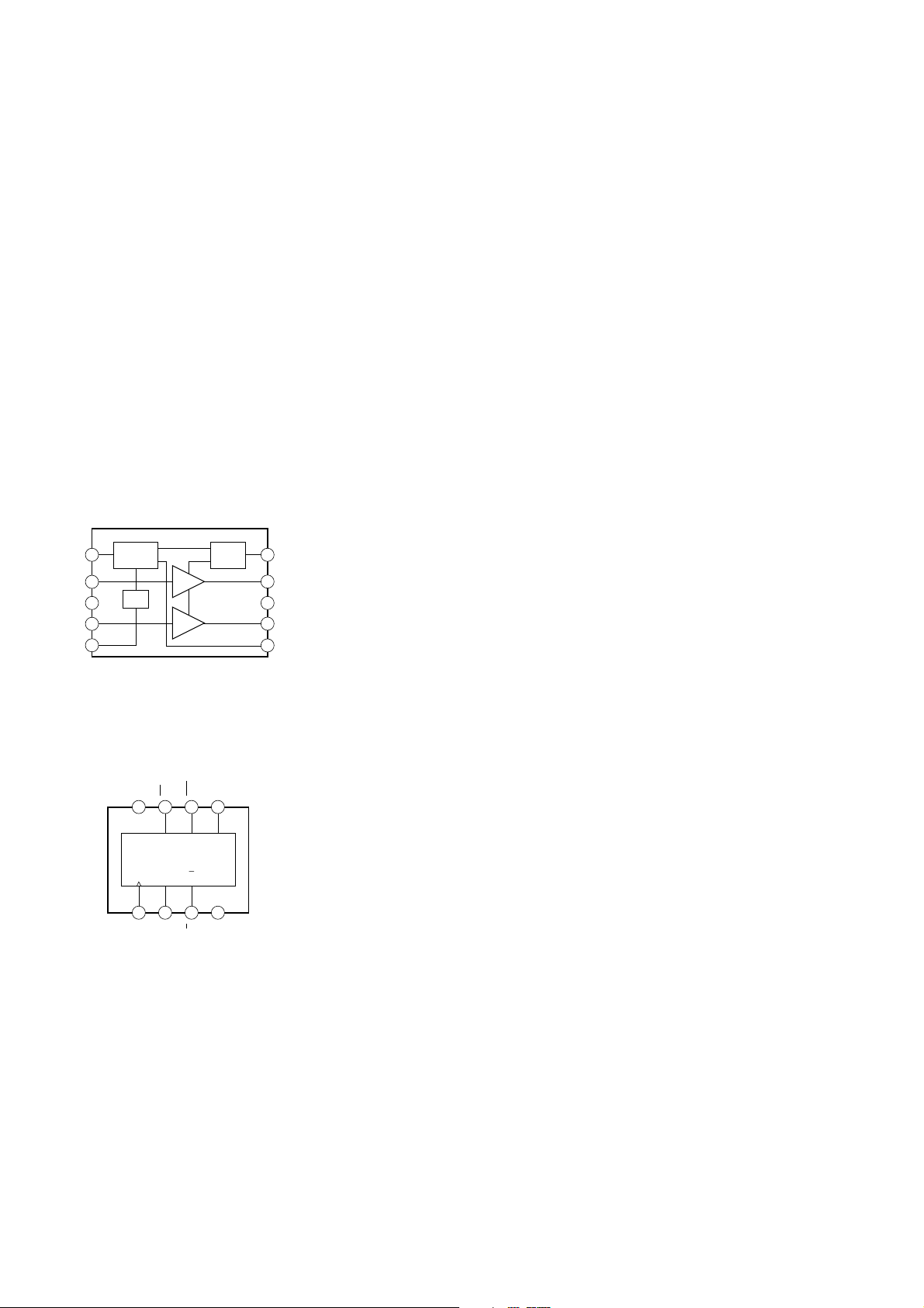
• IC BLOCK DIAGRAMS
IC302 LA4533M TP-1
4
W or less unless otherwise specified.
P/SW
IN1
PRE GND
IN2
REF
SWITCH
2
BIAS
3
4
5
AMP1
AMP2
POWER
1
IC305 TC7W74FU (TE12R)
CLR
PR
VCC
8
1
CK
6
7
RSQ
QDC
3Q2
D
MUTE
CIRCIUT
Q
5
4
GND
10
MT/SW
OUT1
9
8
POWER GND
7
OUT2
6
VCC
10
Page 11

4-1. BLOCK DIAGRAMS
MDR-RF975R
ANT301
RX-BASE BOARD
FRONT END
FE UNIT
D301
18
RECEIVE
+V
L301
FREQ.
20
FM FE
22
+V
L302
IC303
COUNTER
CF301
CF302
10.7MHz
REG
21
+V
1316
26
OSC
Q301
FM IF/
DISCRI
SWITCH
Q303
AUTO
BLEND
MUTE
IF AMP/DECODE
IC301
PD1
COUNTER
PD1
FREE RUN
1/2
VCO
27
RV301
FREQ.
DECODE
AMP
MONO/ST
SW
DETUNE
MUTE
STEREO
IND
TUNING
IND
IC307
(L-CH)
IC308
Q306
6 2
5
10
HPF
R-CH
DETECT
IC304
IC309
LPF EQ
IC306
(R-CH)
EXPANDER
AMP
RV302
VOL
w
IC305
Q
FF
12
Q305
D
Q
S301
TUNE
RX-SW BOARD
B+
D304
power
• Signal path.
: FM
: AUDIO
• R-ch is omitted due to same as L-ch.
POWER AMP
IC302
10
MUTE
Q304
S1
ON/OFF SW
RECHAGEABLE BATTERY
(NICKEL-CADMIUM)
NH-AAC
2PCS, 2.4V
9
R-CH
SPEAKER
L-CH
SPEAKER
R-CH
+
CHARGE
TERMINAL
(TO TMR-RF975R)
–
11
11
Page 12

MDR-RF975R
4-2. SCHEMATIC DIAGRAM
C311
10
16V
RV301
4.7k
FREE
RUN
CXA1538N
IC301
C302
0.47
C304
0.001
FREQ.
R310
3.3k
C301
1
IF AMP/DECODE
R304
3.3k
C303
4.7/16V
R302
2.2k
• See page 10 for Notes. • See page 10 for IC Block Diagrams.
D301
CF302
10.7MHz
DISC
C381
4.7
16V
C305
0.001
C380
16V
1T363
C312
R312
3.3
15k
50V
C359
0.001
C314
C313
0.01
JC311
0
C306
R305
22
3.3k
16V
R370
8.2k
4.7
C370
1000p
1000p
R374
4.3k
C379
2200p
R372
R373
8.2k
8.2k
C373
C372
1000p
1000p
R375
4.3k
R330
68p
C333
3p
10
C307
0.01
C378
2200p
R371
8.2k
C371
C315
C320
R309
100k
C316
10
0.1
16V
µH
L301
10p
AIR COIL
L302
0.33
C308
22
16V
C310
C309
1
1
50V
50V
R376
100k
Q306
2SC2712L
HPF
R380
1.0k
R377
100k
R400
C355
0.001
C319
0.01
C354
0.01
CF301
10.7MHz
R382
2.2k
R383
2.2k
R331
2.2k
R384
5.6k
C384
2200p
R385
5.6k
C385
2200p
C352
0.001
C329
0.01
LPF
IC309
NJM2100E
C388
150pF
C317
0.001
C336
56p
C332
56p
R325
330
C331
1
100
R401
100
C353
0.01
C382
1
Q307
2SC2712L
HPT
C383
1
R381
1k
C386
0.022
R386
4.7k
C387
0.022
R387
4.7k
R308
2.2k
R320
10
R366
150
D303
UDZ-TE-17-2.2B
C346
0.22
JC304
C347
0
47
16V
C340
R340
0.1
8.2k
COUNTER
R342
R341
240k
470k
IC303
TC74HC4024
30k
15k
7.5k
R345
R346
R347
R348
47k
C337
100p
R403
10k
R391
100k
R390
100k
R404
C404
10k
C389
150pF
1
C400
R343
120k
0.1
62k
R344
F
R349
ANT301
ANTENNA
FE UNIT
(FRONT END)
R356
22k
JC303
0
JC306
R367
47k
R353
R352
R351
R350
15k
C342
0.01
C341
0.1
10k
R392
3.9k
R393
2.2k
C377
2.2
C376
220p
Q301
FMW1
OSC
C375
R378
3.9k
R379
2.2
1M
15k
1M
C343
0.01
IC304
Q303
2SC2712L
OSC SWITCH
C391
2.2
C374
220p
2.2k
EQ AMP
IC306
NJM2100E
C392
2.2
C394
C393
10
16V
JC350
0
1000p
C356
10
16V
0
BA10393F
4
3
2
1
4
3
2
1
GND
CAP
REF
REFERENCE
60K
SUN IN
NFIN
GND
CAP
REF
REFERENCE
60K
SUN IN
NFIN
22k
47k
R358
R355
RECTIFIER
GAIN CELL
TK10691M
RECTIFIER
TK10691M
DETECT
R357
22k
IC307
GAIN CELL
IC308
R354
R364
C402
0.022
R395
3.3k
R394
3.3k
C403
0.022
R396
22k
R362
10k
R363
22k
1
C321
27k
R398
10k
R397
27k
RV302(1/2)
0.01
C318
R399
10k
RV302(2/2)
1
C322
C330
R333
2.2k
C361
100p
R334
2.2k
C362
100p
33
25V
R332
1.0k
FF
C345
0.1
IC305
C399
0.01
C344
TC7W74FU
0.1
Q305
DTC114TK
BUFFER
EXPANDER
AMP
C397
2.2
C395
1
EXPANDER
AMP
C398
2.2
C396
1
R361
22k
22k
R360
22k
S301
TUNE
CAP
RECT
5
20K
IN
6
CONT
20K
7
SUM
8
VCC
CAP
RECT
5
20K
IN
6
CONT
20K
7
SUM
8
VCC
RV302
2SC2712L
AUDIO MUTE
R318
47k
P S/W
IN1
PRE
GND
IN2
REF
POWER AMP
IC302
LA4533M
Q304
MT/SW
OUT1
POWER
OUT2
GND
VCC
C323
R314
100k
JC309
C357
0.01
0.1
C325
220
JC331
6.3V
0
0
C324
C326
220
JC332
6.3V
0
RECHARGEABLE
D304
TLSU124
power
(NICKEL-CADMIUM)
R316
10
10
R315
C327
0.1
220
6.3V
JC334
C328
0.1
JC333
0
0
R321
1.5k
BATTERY
NH-AAC
2pcs,2.4V
R322
6.8k
C363
0.01
JC336
JC335
0
0
D310
RB411D
+
SPEAKER
(L-ch)
-
+
SPEAKER
(R-ch)
-
S302
(POWER ON/OFF)
+
TO
TMR-RF975R
(BATTERY
CHARGE
TERMINAL)
-
12
12
Page 13

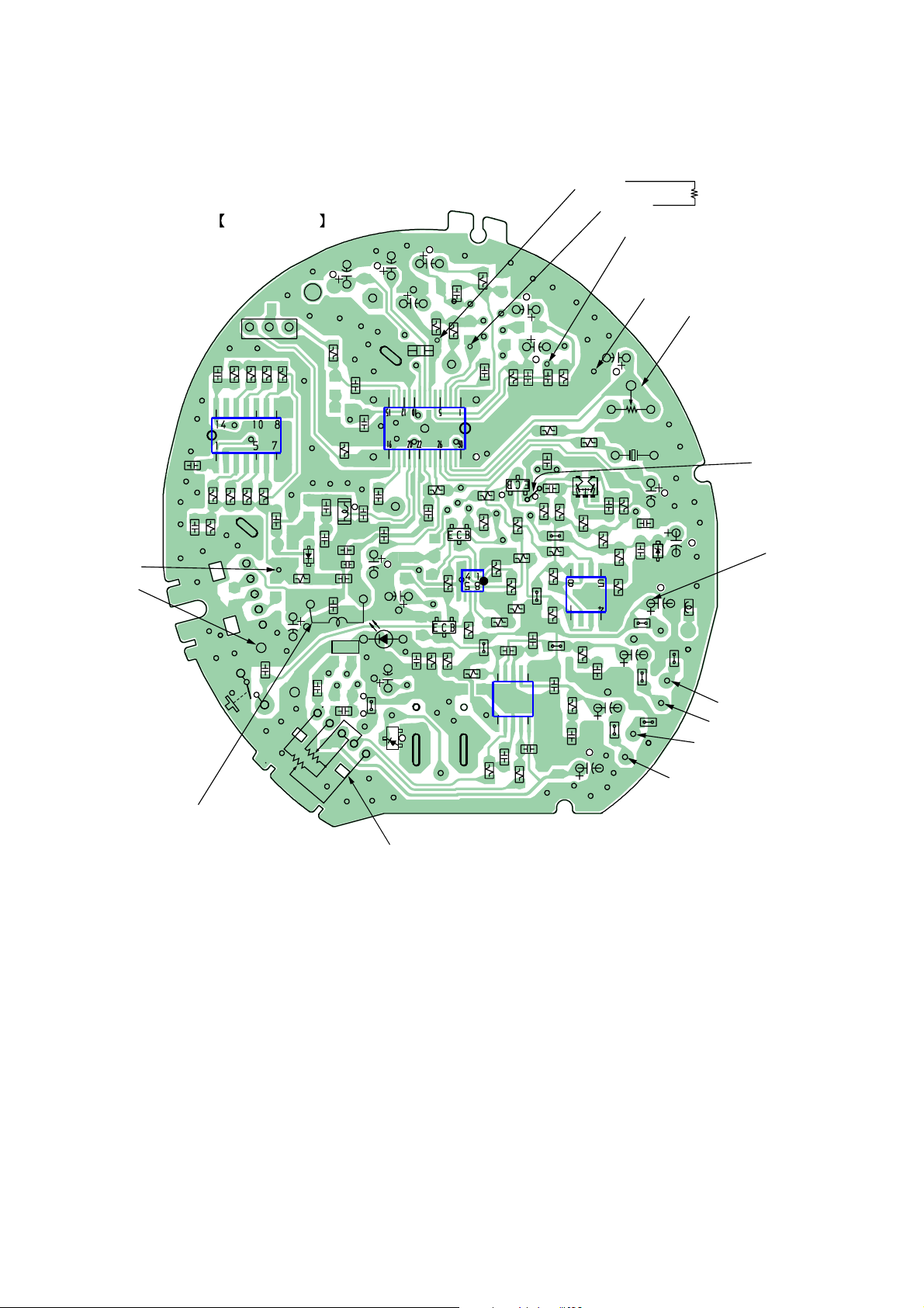
4-3. PRINTED WIRING BOARD
MDR-RF975R
1
2
3 4 5 6 7
8
9 10
• Semiconductor
A
ANT301
RX-BASE BOARD (SIDE A)
RX-BASE BOARD (SIDE B)
C303
(ANTENNA)
C309
R325
C329
C340
R340
R341
CF301
R342
R343
B
IC303
C331
R308
C
C337
C341
D
E
F
S301
TUNE
R346
R345
R347
R349
S301
R344
C320
C344
RV302
VOL
w
RECHAGEABLE BATTERY
(NICKEL-CADMIUM)
D301
R312
C316
L301
C322
NH-AAC
2PCS, 2.4V
C332
C336
C313
C315
C314
D304
power
C321
C319
L302
C317
C312
C394
C355
JC335
D310
C308
R302
C307
C302
R320
R330
C301
C306
IC301
R309
R348
C333
Q305
C359
Q304
C393
R322
C363
+
TO TMR-RF975R
(BATTERY CHARGE TERMINAL)
IC305
R318
R321
R314
–
R331
R363
R361
R360
C323
JC303
10 6
IC302
15
R333
C381
R304
R310
Q303
R354
R362
R364
R332
C362
C361
1-677-934-
C304
R334
C380
C352
C343
R353
JC306
R367
C345
JC309
C305
R355
C328
R305
JC311
Q301
R352
R351
JC304
R358
IC304
R315
C357
R316
C330
11
(11)
R366
C327
C311
C342
JC336
JC332
RV301
C326
CF302
R350
R356
R357
JC334
C310
C346
C325
JC331
FE UNIT
(FRONT-END)
C318
C347
D303
C324
JC333
–
+
–
+
RX-SW BOARD
S302
(POWER ON/OFF)
1-678-658-
(11)
11
SPEAKER
(L-CH)
SPEAKER
(R-CH)
R401
C354
Q307
R381
C384
C353
R400
R383
C383
R385
R380
C372
C404
R372
R404
R387
C387
C385
C377
C382
R390
R393
C378
Q306
R377
IC309
C389
IC306
R374
R382
R384
R403
R391
R379
C388
R392
C376
R370
R371
R375
R378
C373
R386
C392
C391
C375
C370
C371
R376
C386
C374
C379
R373
IC308
JC350
C400
C398
C395
IC307
C399
C396
C356
R395
1-677-934-
C397
C402
C403
R394
R397
R396
R399
R398
11
(11)
Location
Ref. No. Location
D301 C-2
D303 D-5
D304 D-3
D310 E-3
IC301 B-3
IC302 E-4
IC303 C-2
IC304 D-4
IC305 D-4
IC306 E-8
IC307 D-8
IC308 D-8
IC309 D-8
Q301 C-4
Q303 C-4
Q304 D-3
Q305 C-3
Q306 C-8
Q307 C-7
13
Note:
• X : parts extracted from the component side.
• a : Through hole.
• : Pattern from the side which enables seeing.
(The other layer's patterns are not indicated.)
Caution:
Pattern face side: Parts on the pattern face side seen from the
(Side B) pattern face are indicated.
Parts face side: Parts on the parts face side seen from the
(Side A) parts face are indicated.
13
Page 14

MDR-RF975R
NOTE:
• -XX, -X mean standardized parts, so they may
have some differences from the original one.
• Items marked “*” are not stocked since they
are seldom required for routine service. Some
delay should be anticipated when ordering these
items.
SECTION 5
EXPLODED VIEWS
• The mechanical parts with no reference number
in the exploded views are not supplied.
• Hardware (# mark) list and accessories and
packing materials are given in the last of this
parts list.
23
24
20
#2
d
not supplied
#1
13
c
14
d
#2
15
4
b
3
6
#2
#2
not
supplied
36
a
#1
e
14
b
a
21
5
37
#1
not
supplied
7
c
#1
12
37
not
supplied
e
22
8
not
supplied
9
37
not
supplied
16
25
37
not
supplied
1
29
2
28
37
33
10
17
6
18
not
supplied
19
32
31
34
#2
4
37
26
35
Ref. No. Part No. Description Remarks Ref. No. Part No. Description Remarks
1 3-224-689-01 SHEET (R), LIGHT PREVENTION
2 3-846-312-01 SPACER
3 X-3379-301-1 CUSHION ASSY, HEAD
4 3-046-718-01 PAD, EAR
5 X-3379-304-1 PLATE (L) ASSY, FRONT
6 X-3380-120-1 DRIVER ASSY
7 3-046-723-01 HOLDER (L), EAR PAD
8 1-756-109-11 BATTERY, NICKEL HYDROGEN
9 3-046-717-01 TERMINAL (SMALL), BATTERY
10 X-3380-844-1 HOUSING (L) ASSY
11 3-046-709-11 CAP (L), ORNAMENTAL
12 3-046-716-01 TERMINAL (LARGE), BATTERY
13 3-046-696-01 HOLDER (L)
14 3-046-695-01 CHASSIS
15 3-046-698-01 LID (L), HOLDER
16 3-220-123-01 PLATE (L), HOUSING ORNAMENTAL
17 3-046-707-01 HOUSING (L)
18 3-049-953-21 LID (L), HANGER
19 3-046-705-01 HANGER (L)
20 3-046-699-01 LID (R), HOLDER
* 21 1-678-658-11 RX-SW BOARD
22 3-046-697-02 HOLDER (R)
23 3-046-706-01 HANGER (R)
24 3-049-954-21 LID (R), HANGER
25 3-046-708-01 HOUSING (R)
26 X-3380-845-1 HOUSING (R) ASSY
* 28 A-3062-570-A RX-BASE BOARD, COMPLETE
29 3-049-797-01 LIGHT, MDR GUIDE
31 3-220-124-01 PLATE (R), HOUSING ORNAMENTAL
32 3-046-715-01 TERMINAL, CHARGE
33 3-049-951-01 KNOB, VOLUME
34 3-046-724-01 HOLDER (R), EAR PAD
35 X-3380-341-1 PLATE (R) ASSY, FRONT
36 3-224-569-01 SPRING (ON/OFF)
37 3-223-909-01 SCREW (B2)
38 3-224-572-01 SHEET, HOLOGRAM (L) ADHESIVE
39 3-224-688-01 SHEET (L), LIGHT PREVENTION
#1 7-627-553-28 SCREW,PRECISION +P 2X2.5
#2 7-685-104-14 SCREW +P 2X6 TYPE2 NON-SLIT
#2
14
Page 15

SECTION 6
ELECTRICAL PARTS LIST
Ref. No. Part No. Description Remarks Ref. No. Part No. Description Remarks
NOTE:
• Due to standardization, replacements in the
parts list may be different from the parts
specified in the diagrams or the components
used on the set.
• -XX, -X mean standardized parts, so they
may have some difference from the original
one.
• Items marked “*” are not stocked since they
are seldom required for routine service.
Some delay should be anticipated when
ordering these items.
Ref. No. Part No. Description Remarks Ref. No. Part No. Description Remarks
* A-3062-570-A RX-BASE BOARD, COMPLETE
*********************
3-046-715-01 TERMINAL, CHARGE
3-049-951-01 KNOB, VOLUME
< CAPACITOR >
C301 1-164-346-11 CERAMIC CHIP 1uF 16V
C302 1-164-005-11 CERAMIC CHIP 0.47uF 25V
C303 1-124-259-11 ELECT 4.7uF 20% 16V
C304 1-163-009-11 CERAMIC CHIP 0.001uF 10% 50V
C305 1-163-009-11 CERAMIC CHIP 0.001uF 10% 50V
C306 1-124-234-00 ELECT 22uF 20% 16V
C307 1-163-059-91 CERAMIC CHIP 0.01uF 10% 50V
C308 1-124-234-00 ELECT 22uF 20% 16V
C309 1-104-942-11 ELECT 1uF 20% 50V
C310 1-104-942-11 ELECT 1uF 20% 50V
C311 1-124-233-11 ELECT 10uF 20% 16V
C312 1-126-162-11 ELECT 3.3uF 20% 50V
C313 1-163-021-91 CERAMIC CHIP 0.01uF 10% 50V
C314 1-164-441-11 CERAMIC CHIP 68PF 5% 50V
C315 1-163-227-11 CERAMIC CHIP 10PF 0.50PF 50V
C316 1-124-233-11 ELECT 10uF 20% 16V
C317 1-163-009-11 CERAMIC CHIP 0.001uF 10% 50V
C318 1-163-021-91 CERAMIC CHIP 0.01uF 10% 50V
C319 1-163-021-91 CERAMIC CHIP 0.01uF 10% 50V
C320 1-163-038-00 CERAMIC CHIP 0.1uF 25V
C321 1-164-346-11 CERAMIC CHIP 1uF 16V
C322 1-164-346-11 CERAMIC CHIP 1uF 16V
C323 1-163-038-00 CERAMIC CHIP 0.1uF 25V
C324 1-124-635-00 ELECT 220uF 20% 6.3V
C325 1-124-635-00 ELECT 220uF 20% 6.3V
C326 1-124-635-00 ELECT 220uF 20% 6.3V
C327 1-163-038-00 CERAMIC CHIP 0.1uF 25V
C328 1-163-038-00 CERAMIC CHIP 0.1uF 25V
C329 1-163-021-91 CERAMIC CHIP 0.01uF 10% 50V
C330 1-124-242-00 ELECT 33uF 20% 25V
C331 1-164-346-11 CERAMIC CHIP 1uF 16V
C332 1-163-245-11 CERAMIC CHIP 56PF 5% 50V
C333 1-163-220-11 CERAMIC CHIP 3PF 0.25PF 50V
C336 1-163-245-11 CERAMIC CHIP 56PF 5% 50V
C337 1-163-251-11 CERAMIC CHIP 100PF 5% 50V
C340 1-163-038-00 CERAMIC CHIP 0.1uF 25V
C341 1-163-038-00 CERAMIC CHIP 0.1uF 25V
C342 1-163-021-91 CERAMIC CHIP 0.01uF 10% 50V
C343 1-163-021-91 CERAMIC CHIP 0.01uF 10% 50V
C344 1-163-038-00 CERAMIC CHIP 0.1uF 25V
• CAPACITORS:
uF: µF
• RESISTORS
All resistors are in ohms.
METAL: metal-film resistor
METAL OXIDE: Metal Oxide-film resistor
F: nonflammable
• COILS
uH: µH
C346 1-164-489-11 CERAMIC CHIP 0.22uF 10% 16V
C347 1-124-589-11 ELECT 47uF 20% 16V
C352 1-163-009-11 CERAMIC CHIP 0.001uF 10% 50V
C353 1-163-021-91 CERAMIC CHIP 0.01uF 10% 50V
C354 1-163-021-91 CERAMIC CHIP 0.01uF 10% 50V
C355 1-163-009-11 CERAMIC CHIP 0.001uF 10% 50V
C356 1-163-009-11 CERAMIC CHIP 0.001uF 10% 50V
C357 1-163-021-91 CERAMIC CHIP 0.01uF 10% 50V
C359 1-163-009-11 CERAMIC CHIP 0.001uF 10% 50V
C361 1-163-251-11 CERAMIC CHIP 100PF 5% 50V
C362 1-163-251-11 CERAMIC CHIP 100PF 5% 50V
C363 1-163-021-91 CERAMIC CHIP 0.01uF 10% 50V
C370 1-163-009-11 CERAMIC CHIP 0.001uF 10% 50V
C371 1-163-009-11 CERAMIC CHIP 0.001uF 10% 50V
C372 1-163-009-11 CERAMIC CHIP 0.001uF 10% 50V
C373 1-163-009-11 CERAMIC CHIP 0.001uF 10% 50V
C374 1-163-259-91 CERAMIC CHIP 220PF 5% 50V
C375 1-164-505-11 CERAMIC CHIP 2.2uF 16V
C376 1-163-259-91 CERAMIC CHIP 220PF 5% 50V
C377 1-164-505-11 CERAMIC CHIP 2.2uF 16V
C378 1-164-161-11 CERAMIC CHIP 0.0022uF 10% 100V
C379 1-164-161-11 CERAMIC CHIP 0.0022uF 10% 100V
C380 1-124-259-11 ELECT 4.7uF 20% 16V
C381 1-124-259-11 ELECT 4.7uF 20% 16V
C382 1-164-346-11 CERAMIC CHIP 1uF 16V
C383 1-164-346-11 CERAMIC CHIP 1uF 16V
C384 1-164-161-11 CERAMIC CHIP 0.0022uF 10% 100V
C385 1-164-161-11 CERAMIC CHIP 0.0022uF 10% 100V
C386 1-163-037-11 CERAMIC CHIP 0.022uF 10% 25V
C387 1-163-037-11 CERAMIC CHIP 0.022uF 10% 25V
C388 1-163-255-11 CERAMIC CHIP 150PF 5% 50V
C389 1-163-255-11 CERAMIC CHIP 150PF 5% 50V
C391 1-164-505-11 CERAMIC CHIP 2.2uF 16V
C392 1-164-505-11 CERAMIC CHIP 2.2uF 16V
C393 1-124-233-11 ELECT 10uF 20% 16V
C394 1-124-233-11 ELECT 10uF 20% 16V
C395 1-164-346-11 CERAMIC CHIP 1uF 16V
C396 1-164-346-11 CERAMIC CHIP 1uF 16V
C397 1-164-505-11 CERAMIC CHIP 2.2uF 16V
C398 1-164-505-11 CERAMIC CHIP 2.2uF 16V
C399 1-163-021-91 CERAMIC CHIP 0.01uF 10% 50V
C400 1-163-038-00 CERAMIC CHIP 0.1uF 25V
C402 1-163-037-11 CERAMIC CHIP 0.022uF 10% 25V
C403 1-163-037-11 CERAMIC CHIP 0.022uF 10% 25V
C404 1-164-346-11 CERAMIC CHIP 1uF 16V
• SEMICONDUCTORS
In each case, u: µ, for example:
uA...: µA... , uPA... , µPA... ,
uPB... , µPB... , uPC... , µPC... ,
uPD..., µPD...
When indicating parts by reference number,
please include the board name.
MDR-RF975R
RX-BASE
C345 1-163-038-00 CERAMIC CHIP 0.1uF 25V
15
Page 16

MDR-RF975R
Ver 1.1 2001.06
RX-BASE
Ref. No. Part No. Description Remarks Ref. No. Part No. Description Remarks
< CERAMIC FILTER >
CF301 1-577-588-11 FILTER, CERAMIC
CF302 1-577-572-11 FILTER, CERAMIC
R320 1-216-001-00 METAL CHIP 10 5% 1/10W
R321 1-216-053-00 METAL CHIP 1.5K 5% 1/10W
R322 1-216-069-00 METAL CHIP 6.8K 5% 1/10W
R325 1-216-037-00 METAL CHIP 330 5% 1/10W
< DIODE >
D301 8-719-002-81 DIODE 1T363
D303 8-719-056-71 DIODE UDZ-TE-17-2.2B
D304 8-719-077-16 LED TLSU124(TPJ52) (power)
D310 8-719-975-40 DIODE RB411D
< IC >
IC301 8-752-072-12 IC CXA1538N
IC302 8-759-802-75 IC LA4533M
IC303 8-759-453-43 IC TC74HC4024AF(EL)
IC304 8-759-510-73 IC BA10393F-E2
IC305 8-759-083-94 IC TC7W74FU
IC306 8-759-344-00 IC NJM2100E(TE2)
IC307 8-759-384-90 IC TK10691M
IC308 8-759-384-90 IC TK10691M
IC309 8-759-344-00 IC NJM2100E(TE2)
< JUMPER RESISTER >
JC303 1-216-295-91 SHORT 0
JC304 1-216-295-91 SHORT 0
JC306 1-216-295-91 SHORT 0
JC309 1-216-295-91 SHORT 0
JC311 1-216-295-91 SHORT 0
JC331 1-216-295-91 SHORT 0
JC332 1-216-295-91 SHORT 0
JC333 1-216-295-91 SHORT 0
JC334 1-216-295-91 SHORT 0
JC335 1-216-295-91 SHORT 0
JC336 1-216-295-91 SHORT 0
JC350 1-216-295-91 SHORT 0
< COIL >
L301 1-422-317-31 COIL, AIR-CORE
L302 1-412-933-11 INDUCTOR 0.33uH
R330 1-216-001-00 METAL CHIP 10 5% 1/10W
R331 1-216-057-00 METAL CHIP 2.2K 5% 1/10W
R332 1-216-049-11 RES-CHIP 1K 5% 1/10W
R333 1-216-057-00 METAL CHIP 2.2K 5% 1/10W
R334 1-216-057-00 METAL CHIP 2.2K 5% 1/10W
R340 1-216-071-00 METAL CHIP 8.2K 5% 1/10W
R341 1-216-113-00 METAL CHIP 470K 5% 1/10W
R342 1-216-106-00 METAL CHIP 240K 5% 1/10W
R343 1-216-099-00 METAL CHIP 120K 5% 1/10W
R344 1-216-092-00 RES-CHIP 62K 5% 1/10W
R345 1-216-084-00 METAL CHIP 30K 5% 1/10W
R346 1-216-077-00 RES-CHIP 15K 5% 1/10W
R347 1-216-070-00 METAL CHIP 7.5K 5% 1/10W
R348 1-216-089-91 RES-CHIP 47K 5% 1/10W
R349 1-216-073-00 RES-CHIP 10K 5% 1/10W
R350 1-216-077-00 RES-CHIP 15K 5% 1/10W
R351 1-216-121-11 RES-CHIP 1M 5% 1/10W
R352 1-216-121-11 RES-CHIP 1M 5% 1/10W
R353 1-216-077-00 RES-CHIP 15K 5% 1/10W
R354 1-216-081-00 METAL CHIP 22K 5% 1/10W
R355 1-216-089-91 RES-CHIP 47K 5% 1/10W
R356 1-216-081-00 METAL CHIP 22K 5% 1/10W
R357 1-216-081-00 METAL CHIP 22K 5% 1/10W
R358 1-216-081-00 METAL CHIP 22K 5% 1/10W
R360 1-216-081-00 METAL CHIP 22K 5% 1/10W
R361 1-216-081-00 METAL CHIP 22K 5% 1/10W
R362 1-216-073-00 RES-CHIP 10K 5% 1/10W
R363 1-216-081-00 METAL CHIP 22K 5% 1/10W
R364 1-216-081-00 METAL CHIP 22K 5% 1/10W
R366 1-216-029-00 METAL CHIP 150 5% 1/10W
R367 1-216-089-91 RES-CHIP 47K 5% 1/10W
R370 1-216-071-00 METAL CHIP 8.2K 5% 1/10W
R371 1-216-071-00 METAL CHIP 8.2K 5% 1/10W
R372 1-216-071-00 METAL CHIP 8.2K 5% 1/10W
R373 1-216-071-00 METAL CHIP 8.2K 5% 1/10W
< TRANSISTOR >
Q301 8-729-903-10 TRANSISTOR FMW1
Q303 8-729-200-72 TRANSISTOR 2SC2712L-TE85L
Q304 8-729-200-72 TRANSISTOR 2SC2712L-TE85L
Q305 8-729-027-44 TRANSISTOR DTC114TKA-T146
Q306 8-729-200-72 TRANSISTOR 2SC2712L-TE85L
Q307 8-729-200-72 TRANSISTOR 2SC2712L-TE85L
< RESISTER >
R302 1-216-057-00 METAL CHIP 2.2K 5% 1/10W
R304 1-216-061-00 RES-CHIP 3.3K 5% 1/10W
R305 1-216-061-00 RES-CHIP 3.3K 5% 1/10W
R308 1-216-057-00 METAL CHIP 2.2K 5% 1/10W
R309 1-216-097-11 RES-CHIP 100K 5% 1/10W
R310 1-216-061-00 RES-CHIP 3.3K 5% 1/10W
R312 1-216-077-00 RES-CHIP 15K 5% 1/10W
R314 1-216-097-11 RES-CHIP 100K 5% 1/10W
R315 1-216-001-00 METAL CHIP 10 5% 1/10W
R316 1-216-001-00 METAL CHIP 10 5% 1/10W
R318 1-216-089-91 RES-CHIP 47K 5% 1/10W
16
R374 1-216-064-00 METAL CHIP 4.3K 5% 1/10W
R375 1-216-064-00 METAL CHIP 4.3K 5% 1/10W
R376 1-216-097-11 RES-CHIP 100K 5% 1/10W
R377 1-216-097-11 RES-CHIP 100K 5% 1/10W
R378 1-216-063-91 RES-CHIP 3.9K 5% 1/10W
R379 1-216-057-00 METAL CHIP 2.2K 5% 1/10W
R380 1-216-049-11 RES-CHIP 1K 5% 1/10W
R381 1-216-049-11 RES-CHIP 1K 5% 1/10W
R382 1-216-057-00 METAL CHIP 2.2K 5% 1/10W
R383 1-216-057-00 METAL CHIP 2.2K 5% 1/10W
R384 1-216-067-00 METAL CHIP 5.6K 5% 1/10W
R385 1-216-067-00 METAL CHIP 5.6K 5% 1/10W
R386 1-216-065-91 RES-CHIP 4.7K 5% 1/10W
R387 1-216-065-91 RES-CHIP 4.7K 5% 1/10W
R390 1-216-097-11 RES-CHIP 100K 5% 1/10W
R391 1-216-097-11 RES-CHIP 100K 5% 1/10W
R392 1-216-063-91 RES-CHIP 3.9K 5% 1/10W
R393 1-216-057-00 METAL CHIP 2.2K 5% 1/10W
R394 1-216-061-00 RES-CHIP 3.3K 5% 1/10W
R395 1-216-061-00 RES-CHIP 3.3K 5% 1/10W
R396 1-216-083-00 METAL CHIP 27K 5% 1/10W
Page 17

MDR-RF975R
RX-BASE
Ref. No. Part No. Description Remarks Ref. No. Part No. Description Remarks
R397 1-216-083-00 METAL CHIP 27K 5% 1/10W
R398 1-216-073-00 RES-CHIP 10K 5% 1/10W
R399 1-216-073-00 RES-CHIP 10K 5% 1/10W
R400 1-216-025-11 RES-CHIP 100 5% 1/10W
R401 1-216-025-11 RES-CHIP 100 5% 1/10W
R403 1-216-073-00 RES-CHIP 10K 5% 1/10W
R404 1-216-073-00 RES-CHIP 10K 5% 1/10W
< VARIABLE RESISTOR >
RV301 1-241-763-11 RES, ADJ, CARBON 4.7K (FREE RUN FREQ.)
RV302 1-227-189-11 RES, VAR CARBON 20K/20K (VOL )
< SWITCH >
S301 1-771-980-11 SWITCH, TACTILE (TUNE)
w
RX-SW
******************************************************
*
1-678-658-11 RX-SW BOARD
***********
< SWITCH >
S302 1-572-467-61 SWITCH, PUSH (1 KEY) (POWER ON/OFF)
******************************************************
MISCELLANEOUS
*************
6 X-3380-120-1 DRIVER ASSY
8 1-756-109-11 BATTERY, NICKEL HYDROGEN
17
Page 18

MDR-RF975R
REVISION HISTORY
Clicking the version allows you to jump to the revised page.
Also, clicking the version at the upper right on the revised page allows you to jump to the next revised
page.
Ver. Date Description of Revision
1.1 2001.06 Correction of electrical adjustment and electrical parts list. (ENG-01007)
1.0 2001.05 New
Page 19

TMR-RF975R
SERVICE MANUAL
Ver 1.1 2001. 06
TMR-RF975R is the component model block one in the MDR-RF975RK.
COMPONENT MODEL NAME FOR MDR-RF975RK
Headphones MDR-RF975R
Transmitter TMR-RF975R
US Model
SPECIFICATIONS
General
Carrier frequency
913.5 – 914.5 MHz
Channel Ch1, Ch2, Ch3
Modulation FM stereo
Frequency response
18 – 22,000 Hz
Transmitter TMR-RF975R
Power source DC 9 V: supplied AC power adaptor
Audio input phono jacks/stereo mini jack
Dimensions Approx. 130 135 150 mm
Mass Approx. 200 g (7 oz.)
Design and specifications are subject to change without
notice.
1
(5
/4 5 3/8 6 in.) (w/h/d)
XX
XX
9-873-140-12
2001F0200-1
© 2001.6
TRANSMITTER
Sony Corporation
Personal Audio Company
Shinagawa Tec Service Manual Production Group
Page 20

TMR-RF975R
TABLE OF CONTENTS
Specifications ............................................................................ 1
1. GENERAL ....................................................................... 2
2. DISASSEMBLY
2-1. Housing (Upper) ....................................................... 3
2-2. TX-BASE Board ....................................................... 3
3. ELECTRICAL ADJUSTMENTS ............................. 4
4. DIAGRAMS
4-1. Block Diagrams ........................................................ 5
4-2. Schematic Diagram– TX-BASE Section – ............... 6
4-3. Printed Wiring Board – TX-BASE Section – .......... 7
4-4. Schematic Diagram
– BATTERY CHARGER Section – .......................... 8
4-5. Printed Wiring Board
– BATTERY CHARGER Section – .......................... 9
5. EXPLODED VIEWS....................................................10
6. ELECTRICAL PARTS LIST.....................................11
SECTION 1
GENERAL
This section is extracted from
instruction manual.
Setting up the
transmitter
Connect the transmitter to audio/video
1
equipment. Select one of the hookups
below depending on the jack type:
To connect to a headphones jack
A
Transmitter
OFF ON
BA
R
AUDIO IN
FILTERNOISE
DC IN 9V
L
to AUDIO IN
A jacks
123
CHANNEL
Right channel
(red)
Connecting cord
(supplied)
Unimatch plug
adaptor
(supplied)
to headphones
jack (stereo
phone jack)
Flexible Circuit Board Repairing
• Keep the temperature of soldering iron around 270°C
during repairing.
• Do not touch the soldering iron on the same conductor of the
circuit board (within 3 times).
• Be careful not to apply force on the conductor when soldering
or unsoldering.
Left channel
(white)
to headphones
jack (stereo
mini jack)
Discman, MD,
WALKMAN*, VCR,
etc.
Notes on chip component replacement
• Never reuse a disconnected chip component.
• Notice that the minus side of a tantalum capacitor may be
damaged by heat.
2
Page 21

SECTION 2
)
)
Housing (upper)
2
CHG-NR board
1
Four screws (P 2
× 6)
DISASSEMBLY
Note: Follow the disassembly procedure in the numerical order given .
2-1. HOUSING (UPPER)
TMR-RF975R
2
Housing (upper)
1
Four screws (P 2
× 8
2-2. TX-BASE BOARD
Housing (upper)
Screw
3
TX-BASE board
1
Screw (P 2
2-3. CHG-NR BOARD
2
× 6
3
Page 22

TMR-RF975R
SECTION 3
ELECTRICAL ADJUSTMENTS
Setting :
AF signal
generator
set
TMR-RF975R
L-CH / R-CH (J402)
Telescopic
antenna
Frequency counter
8 cm
set
TMR-RF975R
Transmission Frequency Check
1. Set the noise filter SW to OFF.
2. Input a signal of 1 kHz, 40 mVrms to only the L-CH (J402).
3. Connect a telescopic antenna to the frequency counter input
and extend the antenna to a length of approximately 8 cm.
4. Place TX-BASE board close to the frequency counter, then
measure the frequencies of CH1, CH2 and CH3 and make
sure the values are as follows:
CH1 : 913.5 MHz ± 200 kHz
CH2 : 914.0 MHz ± 200 kHz
CH3 : 914.5 MHz ± 200 kHz
When the frequency does not satisfy the specified value,
set the channel switch (S402) to CH2, then adjust the value of
the frequency counter to 914.0 MHz by trimmer capacitor in
the VCO unit.
Standard value :913.9MHz to 914.1MHz.
Pilot Signal and MPX Signal Modulation Check and
Adjustment
1. Set the channel to CH2.
2. An electric wave is output for 5 or 10 minutes when OFF to ON
a power supply with no signal input (Power indicator will ON).
3. Set the RV402 and RV403 to max. (clockwise)
4. Connect a digital voltmeter (AC range) to the center terminal
of RV403 (Fig.2).
5. Adjust the value of the digital voltmeter to minimum by RV401.
6. See the RV402 to minimum. (counter clock wise)
7. Adjust the value of the digital voltmeter to max by L407.
8. Adjust the value of the digital voltmerter to 2.1to 2.6mVrms
by RV403.
9. Connect a digital voltmeter (AC range) with LPF to movable
terminal of RV403 (Fig.2).
10. Input a signal of 1 kHz, 316 mVrms to only the L-CH.
11. Adjust the value of the digital voltmeter to 5.2 to 6.4 mVrms
by RV402.
Connection points and Adjustment Location :
CH3
L407
←
CH2 ←CH1
S402
RV403RV402
(L-CH) (R-CH)
Sheet
R464
J402
VCO
UNIT
CHG-NR board
When completed with replacement, recheck the frequecies of
CH1, CH2 and CH3.
Compresser Output Check
1. Set the channel to CH2.
2. Input a signal of 1 kHz, 316 mVrms to L-CH and R-CH of
J402.
3. Measure IC 601 pin 7 and IC 602 pin 7 on the CHG-NR
board using a digital voltmeter (AC range) and put down a
value mesured. (Fig.1).
4. Input a signal of 1 kHz, 31.6 mVrms to L-CH and R-CH of
J402.
5. Measure IC 601 pin 7 and IC 602 pin 7 on the CHG-NR
board using a digital voltmeter (AC range) and put down a
value mesured (Fig.1).
Confirm that there is a difference of step 3 and 5 by 10dB±
3dB.
6. When the frequency is not satisfied the specified value,
exchange TX- BASE board or CHG-NR board.
RV401-403,
L407
Modulation
check and
adjustment.
digital
voltmeter
(AC range)
R464
(Fig. 2)
RV401
+
–
Hole
Trimmer capacitor:
Transmission
frequency
adjustment
digital
voltmeter
(AC range)
(Fig. 1)
+
–
1
4
IC 601
7 pin
IC 602
8
5
8
1
5
4
4
Page 23

4-1. BLOCK DIAGRAMS
SECTION 4
DIAGRAMS
TMR-RF975R
B
AUDIO IN
A
TX-BASE BOARD
J401
R-CH
J402
L
R R-CH
S401
NOISE FILTER
OFF
|
ON
NOISE
FILTER
CHG-NR BOARD
IC401
IC601
(L-CH)
IC602
(R-CH)
RV401
CH1
AMP
CH2
AMP
MODULATION
12 11
TIME
DEVISION
MPX
BUFFER
OSC
AMP
76
X401
38kHz
BUFFER
Q401
10
VS
BUFFER
DIVIDER
D404,405
RECT
2V
D408
RV402
9
MODULATION
L407
8
MODULATION
B+
5V
Q402,405
INPUT
DET
Q403
MODULATION
CHANNEL
SET
Q408
RV403
MODULATION
1
2
3
I
S402
CHANNEL
MOD IN
VCO401
(VCO UNIT)
ANT
ANT401
O
IC402
V
5V
+5V
REG
D401
power
SWITCH
Q404
POWER
ON/OFF
Q406,407
CHG-NR BOARD
SWITCH
Q601
IC604(1/2)
DETECT
IC603
D407
SWITCH
Q602
D402
chg
SWITCH
Q604
COMPARATOR
(2/2)
OSC
Q605
IC605
+5V
REG
IC604(2/2)
DETECT
SWITCH
Q603
REF V
+
CHARGE
TERMINAL
–
(TO MDR-RF975R)
J404
DC IN 9V
(1/2)
IC403
STEREO MPX
LPF
R-CH
14
1
72113
• R-ch is omitted due to same as L-ch.
• Signal path.
L : AUDIO
F : FM
5
5
Page 24

TMR-RF975R
4-2. SCHEMATIC DIAGRAM –TX-BASE SECTION –
AUDIO IN
J402
A
-N
G
CH
D
AR
BO
602)
(CN
-N
G
CH
D
AR
BO
601)
N
(C
J404
DC IN 9V
J401
B
R
L
R
B-B CON 3P
R
CNP402
B-B CON
6PIN
CNP401
R411
33k
R401
33k
R414
33k
JW401
JW402
JW406
R404
33k
S401
NOISE FILTER
OFF
D403
11ES2-TA1B
JW416
JW407
R418
2.2k
R448
1k
R458
1k
4.7k
SLR342MGT
D402
R408
2.2k
C413
0.001
R417
1k
R449
15k
R459
15k
chg
C433
C443
1
1
C403
0.001
IC403
NJM2035M
MPX
R406
33k
R416
33k
R407
R403
1k
51
R413
51
ON
L408
R457
19KLPF
R446
1.2k
C480
0.01
R456
1.2k
C432
0.0056
C442
0.0056
L409
19KLPF
JC403
R474
620
0
4.7k
R461
0.022
C416
JW404
R423
220
C417
2.2
50V
L402
L401
R421
100k
R422
3.3k
C431
10
16V
RV401
47k
C453
10
16V
C462
100p
R424
3.3M
C469
C454
100p
C421
16V
0.1
22
L405
C458
10
16V
C423
C459
510p
R468
1.8k
X401
38K
100p
C422
IC401
BA3308F
R440
R432
2.2M
C425
C428
100p
Q401
C427
0.01
R433
22k
Q403
2SC2712L
MODULATION
R471
1.2k
R464
1k
1k
R441
2.2k
R472
470
R490
6.8k
Q401,402
AUDIO INPUT
C430
4.7
16V
D404
1SS133T
C429
100p
D407
MTZ-77-5.6B
DET
D405
1SS133T
C444
100p
C445
100p
R438
220k
R484
1.3k
R485
1.2k
R452
22k
Q408
DTA124KA
CHANNEL
C439
1
R483
2.2k
R486
18k
SET
PRE AMP
JW405
JW403
R428
680
R425
100k
R426
3.3k
C441
10
16V
220
R430
16V
R429
10k
L406
5mH
C455
10p
C460
390p
10k
C456
0.0033
C406
0.022
R427
220
C407
2.2
50V
C426
0.01
D408
MTZ-77-2.0B
C457
0.1
C461
0.0015
R469
33k
L407
20mH
MODULATION
C466
0.01
RV402
R470
33k
RV401-403
2SC2712L
R431
4.7k
0.022
C451
220
16V
JC430
0
10k
RV403
4.7k
R454
47k
R453
680k
Q402
2SC2712L
C436
10
16V
R482
22k
POW
Q405-407
ER ON/OFF
Q405
KTA1266-GR
D410
MA77
2SC2712L
0.0033
S402
CHANNEL
Q407
3
2
1
C452
100
16V
C478
JW413
2SC2712L
D409
MA77
R455
1k
Q406
VCO401
VCO UNIT
JW410
914MHZ
C470
47
16V
R466
22k
JW409
RD5.1ES
D406
L410
C440
100p
Q404
KTA1266-GR
POWER
SWITCH
R467
4.7k
SLR342VCT7
R489
18k
D401
power
C483
R473
620
2p
0.1
C475
C468
0.01
+5V REG
JW411
IC402
KIA78S05
JW415
ANT401
(ANTENNA)
Note on schematic diagrams.
Note:
• All capacitors are in F unless otherwise noted. pF: F 50 WV or
less are not indicated except for electrolytics and tantalums.
• All resistors are in and 1/
• : B+ Line.
4
W or less unless otherwise specified.
• : adjustment for repair.
• Power voltage is dc 9V and fed with regulated dc power supply
from external power voltage jack.
• Voltages are dc with respect to ground under no-signal conditions.
6
6
• Voltages are taken with a VOM (Input impedance 10 M ).
• Signal path.
: FM
: AUDIO
Page 25

4-3. PRINTED WIRING BOARD –TX-BASE SECTION –
TMR-RF975R
1
2
A
TX-BASE BOARD
S401
J401
B A
NOISE FILTER
OFF
TON
CHG-NR
BOARD
R403
(CN601)
B
R413
B
JW401
R414
R407
CNP401
3
2
1
C
C425
R423
C416
R422
C426
R417
R429
D
A
CHG-NR
BOARD
(CN602)
E
C417
R421
Q401
C429
C466
R404
C413
JW404
C421
C431
CNP402
R430
R431
C427
C428
JW402
R418
R424
6
1
R432
C430
L402
IC401
C423
L405
C422
R428
JW405
R433
R440
C445
D404
R490
R406
L401
R456
C444
D405
R416
C403
R446
C436
R411
R401
JW403
C441
L408
C432
C442
L409
R438
R452
JW407
3 4 5
ANT401
ANTENNA
DC IN 9V
JW417
R464
C433
RV401
C453
JC403
J404
C460
C461
C469
IC403
C462
D403
JW416
RV403
L406
C454
R467
C480
R485
R486
R483
R470
R468
C459
C458
C457
X401
C455
AUDIO IN
R408
C407
R427
R426
C406
R425
D406
R455
Q402
R
C483
R453
R454
Q407
R441
L410
C440
Q405
D407
J402
O
V
I (TP12)
R457
R461
JW410
D401
power
D402
chg
C470
VCO401
(VCO UNIT)
R448
C452
C478
Q406
R473
R474
L
R482
C439
R449
D410
D409
JW420
R458
R459
C443
JW409
S402
CHANNEL
1t2t3
JW415
JW413
Q408
Q403
RV402
ECB
R471
C456
R469
JW411
11
(11)
R484
C451
IC402
1
2
3
R472
JC430
L407
JW412
D408
Q404
R466
C468
C475
• Semiconductor
Location
Ref. No. Location
D401 E-3
D402 E-3
D403 B-4
D404 E-2
D405 E-2
D406 D-3
D407 E-3
D408 D-5
D409 D-4
D410 D-4
IC401 C-2
IC302 B-5
IC303 D-4
Q401 D-2
Q402 D-3
Q403 C-5
Q404 C-5
Q405 D-3
Q406 D-4
Q407 D-3
Q408 C-5
R489
Note:
• X : parts extracted from the component side.
• : Pattern from the side which enables seeing.
1-682-266-
7
7
Page 26

TMR-RF975R
4-4. SCHEMATIC DIAGRAM –BATTERY CHARGER SECTION –
CHARGE
TERMINAL
TO
)
MDR-RF975R
470
R636
D601
UDZ S 5.6B
Q601
2SB1386
2.2k
SWITCH
R624
+
Q602
C630
)
-
0.01
DTC144EKA
SWITCH
470
R637
470
R638
470
R639
R621
22k
BA10393
DETECT
470
R640
IC604
• See page 6 for Note.
Q603
DTA144VKA
SWITCH
22k
39k
R625
R635
68k
R627
18k
R628
47k
R626
C626
+5V REG
KIA78S05
0.1
IC605
C621
0.027
R632
TO
TX-BASE BOARD
CNP401
LED
DECT
9V
CN601
HOUSING 3P
C624
47
16V
10k
R629
COMPARATOR
IC603
TB1004AF
C623
0.033
R630
1M
15k
1M
R634
C622
Q605
FMW1
OSC
R631
1
1M
15k
R633
3
1
C627
0.1
C620
0.1
Q604
DTC144EKA
SWITCH
TX-BASE BOARD
GND
1
CNP402
L-IN
TO
R-IN
JC605
0
L-OUT
R601
3.3k
R611
3.3k
R-OUT
5V
6
R602
2.2k
0
JC601
R612
2.2k
0
JC602
CN602
HOUSING 6P
100p
C609
100p
C619
R603
22k
C602
10
16V
R613
22k
C612
10
16V
C601
16V
10
C606
C611
16V
10
C616
R604
22k
R605
10k
R615
10k
0
JC606
C618
16V
22
IC601
TK10690MTL
1
C628
1000p
R614
22k
IC602
TK10690MTL
AMP
1
C629
1000p
C603
16V
C604
C613
10
16V
C614
AMP
C605
10
2.2
C607
0.1
1
C615
2.2
C617
0.1
1
IC601, IC602 TK10690M
8
IC603 TB1004AF(EL)
OSC1
OSC2
OSC3
CMP-
GND
1
2
3
4
CK Q22
R
SQ
SQ
RQ
R
22BIT COUNTER
INITIALIZE
Q
CK
R
SQ
R
Q
CK
R
5
10 VDD
*
9
TIMER OUT1
*
8
TIMER OUT2
7
CMP+
6
RESET
8
Page 27

4-5. PRINTED WIRING BOARD –BATTERY CHARGER SECTION –
TMR-RF975R
A
B
1
CHG-NR BOARD
C602
C606
C628
IC601
C603
C629
C612
C604
C614
R603
R604
C607
IC602
C613
JC601
C605
JC606
JW602
R605
R613
R602
C601
C616
R614
C615
R601
C609
R612
C611
C617
R615
2
JC602
6
C619
R611
JC605
CN602
C630
L601
R636
R637
R638
R640
R639
3 4
Q605
R633
JW601
Q601
R627
R626
JW604
D601
R628
R625
R621
R635
Q603
C622
IC604
R624
2 1 3
IC605
R634
R631
Q602
R629
C626
C624
R632
C621
C623
IC603
Q604
R630
• Semiconductor
Location
Ref. No. Location
D601 B-3
IC601 A-1
IC602 B-1
IC603 B-4
IC604 B-4
IC605 B-4
Q601 B-3
Q602 B-4
Q603 B-3
Q604 B-4
Q605 A-4
C
C618
A
TX-BASE
BOARD
(CNP402)
C627
+
–
CHARGE TERMINAL
(TO MDR-RF975R)
3
JW603
CN601
1-677-935-
C620
B
TX-BASE
BOARD
(CNP401)
11
(11)
9
9
Page 28

TMR-RF975R
NOTE:
• -XX, -X mean standardized parts, so they may
have some differences from the original one.
• Items marked “*” are not stocked since they
are seldom required for routine service. Some
delay should be anticipated when ordering these
items.
SECTION 5
EXPLODED VIEWS
• The mechanical parts with no reference number
in the exploded views are not supplied.
• Hardware (# mark) list and accessories and
packing materials are given in the last of this
parts list.
1
2
5
10
3
11
4
#1
6
7
#1
#1
#1
8
9
#2
#2
Ref. No. Part No. Description Remarks Ref. No. Part No. Description Remarks
1 X-3380-843-1 HOUSING (UPPER) ASSY
2 3-049-798-01 CUSHION, ANTENNA
3 3-046-726-01 LIGHT, GUIDE,
8 X-3380-842-1 CABINET ASSY, LOWER
9 4-984-729-01 FOOT, RUBBER
10 3-673-766-11 CUSHION, UPPER LID
* 4 A-3062-567-A TX-BASE BOARD, COMPLETE
* 5 A-3062-568-A CHG-NR BOARD, COMPLETE
6 3-048-485-01 TERMINAL (+), CHARGE
7 3-048-486-01 TERMINAL (-), CHARGE
11 4-213-164-01 TERMINAL, ANTENNA
#1 7-685-104-19 SCREW +P 2X6 TYPE2 NON-SLIT
#2 7-685-105-19 SCREW +P 2X8 TYPE2 NON-SLIT
10
Page 29

SECTION 6
ELECTRICAL PARTS LIST
Ref. No. Part No. Description Remarks Ref. No. Part No. Description Remarks
NOTE:
• Due to standardization, replacements in the
parts list may be different from the parts
specified in the diagrams or the components
used on the set.
• -XX, -X mean standardized parts, so they
may have some difference from the original
one.
• Items marked “*” are not stocked since they
are seldom required for routine service.
Some delay should be anticipated when
ordering these items.
Ref. No. Part No. Description Remarks Ref. No. Part No. Description Remarks
* A-3062-568-A CHG-NR BOARD, COMPLETE
• CAPACITORS:
uF: µF
• RESISTORS
All resistors are in ohms.
METAL: metal-film resistor
METAL OXIDE: Metal Oxide-film resistor
F: nonflammable
• COILS
uH: µH
• SEMICONDUCTORS
In each case, u: µ, for example:
uA...: µA... , uPA... , µPA... ,
uPB... , µPB... , uPC... , µPC... ,
uPD..., µPD...
When indicating parts by reference number,
please include the board name.
< JUMPER RESISTOR >
TMR-RF975R
CHG-NR
*********************
JC601 1-216-295-91 SHORT 0
3-048-485-01 TERMINAL (+), CHARGE
3-048-486-01 TERMINAL (-), CHARGE
< CAPACITOR >
C601 1-164-346-11 CERAMIC CHIP 1uF 16V
C602 1-126-157-11 ELECT 10uF 20% 16V
C603 1-126-157-11 ELECT 10uF 20% 16V
C604 1-164-346-11 CERAMIC CHIP 1uF 16V
C605 1-164-505-11 CERAMIC CHIP 2.2uF 16V
C606 1-126-157-11 ELECT 10uF 20% 16V
C607 1-163-038-00 CERAMIC CHIP 0.1uF 25V
C609 1-163-251-11 CERAMIC CHIP 100PF 5% 50V
C611 1-164-346-11 CERAMIC CHIP 1uF 16V
C612 1-126-157-11 ELECT 10uF 20% 16V
C613 1-126-157-11 ELECT 10uF 20% 16V
C614 1-164-346-11 CERAMIC CHIP 1uF 16V
C615 1-164-505-11 CERAMIC CHIP 2.2uF 16V
C616 1-126-157-11 ELECT 10uF 20% 16V
C617 1-163-038-00 CERAMIC CHIP 0.1uF 25V
C618 1-124-234-00 ELECT 22uF 20% 16V
C619 1-163-251-11 CERAMIC CHIP 100PF 5% 50V
C620 1-163-038-00 CERAMIC CHIP 0.1uF 25V
C621 1-163-986-00 CERAMIC CHIP 0.027uF 10% 25V
C622 1-164-346-11 CERAMIC CHIP 1uF 16V
C623 1-163-989-11 CERAMIC CHIP 0.033uF 10% 25V
C624 1-126-786-11 ELECT 47uF 20% 16V
C626 1-163-038-00 CERAMIC CHIP 0.1uF 25V
C627 1-163-038-00 CERAMIC CHIP 0.1uF 25V
C628 1-163-009-11 CERAMIC CHIP 0.001uF 10% 50V
C629 1-163-009-11 CERAMIC CHIP 0.001uF 10% 50V
C630 1-163-021-91 CERAMIC CHIP 0.01uF 10% 50V
< CONNECTOR >
* CN601 1-794-571-11 HOUSING, CONNECTOR
JC602 1-216-295-91 SHORT 0
JC605 1-216-295-91 SHORT 0
JC606 1-216-295-91 SHORT 0
< COIL >
L601 1-412-933-11 INDUCTOR 0.33uH
< TRANSISTOR >
Q601 8-729-025-88 TRANSISTOR 2SB1386-T100-R
Q602 1-801-806-11 TRANSISTOR DTC144EKA
Q603 8-729-027-40 TRANSISTOR DTA144VKA-T146
Q604 1-801-806-11 TRANSISTOR DTC144EKA
Q605 8-729-903-10 TRANSISTOR FMW1
< RESISTOR >
R601 1-216-061-00 RES-CHIP 3.3K 5% 1/10W
R602 1-216-057-00 METAL CHIP 2.2K 5% 1/10W
R603 1-216-081-00 METAL CHIP 22K 5% 1/10W
R604 1-216-081-00 METAL CHIP 22K 5% 1/10W
R605 1-216-073-00 RES-CHIP 10K 5% 1/10W
R611 1-216-061-00 RES-CHIP 3.3K 5% 1/10W
R612 1-216-057-00 METAL CHIP 2.2K 5% 1/10W
R613 1-216-081-00 METAL CHIP 22K 5% 1/10W
R614 1-216-081-00 METAL CHIP 22K 5% 1/10W
R615 1-216-073-00 RES-CHIP 10K 5% 1/10W
R621 1-216-081-00 METAL CHIP 22K 5% 1/10W
R624 1-216-057-00 METAL CHIP 2.2K 5% 1/10W
R625 1-216-689-11 METAL CHIP 39K 0.50% 1/10W
R626 1-216-089-91 RES-CHIP 47K 5% 1/10W
R627 1-216-093-00 RES-CHIP 68K 5% 1/10W
R628 1-216-079-00 METAL CHIP 18K 5% 1/10W
R629 1-216-073-00 RES-CHIP 10K 5% 1/10W
R630 1-216-121-11 RES-CHIP 1M 5% 1/10W
R631 1-216-077-00 RES-CHIP 15K 5% 1/10W
R632 1-216-121-11 RES-CHIP 1M 5% 1/10W
* CN602 1-794-571-21 HOUSING, CONNECTOR
< DIODE >
D601 8-719-069-55 DIODE UDZSTE-175.6B
< IC >
IC601 8-759-384-88 IC TK10690M
IC602 8-759-384-88 IC TK10690M
IC603 8-759-678-31 IC TB1004AF(EL)
IC604 8-759-510-73 IC BA10393F-E2
IC605 8-759-537-90 IC KIA78S05P-TP
R633 1-216-121-11 RES-CHIP 1M 5% 1/10W
R634 1-216-077-00 RES-CHIP 15K 5% 1/10W
R635 1-216-081-00 METAL CHIP 22K 5% 1/10W
R636 1-249-413-11 CARBON 470 5% 1/4W
R637 1-249-413-11 CARBON 470 5% 1/4W
R638 1-249-413-11 CARBON 470 5% 1/4W
R639 1-249-413-11 CARBON 470 5% 1/4W
R640 1-249-413-11 CARBON 470 5% 1/4W
******************************************************
11
Page 30

TMR-RF975R
Ver 1.1 2001.06
TX-BASE
Ref. No. Part No. Description Remarks Ref. No. Part No. Description Remarks
* A-3062-567-A TX-BASE BOARD, COMPLETE
*********************
3-673-766-11 CUSHION, UPPER LID
< CAPACITOR >
C403 1-163-009-11 CERAMIC CHIP 0.001uF 10% 50V
C406 1-163-037-11 CERAMIC CHIP 0.022uF 10% 25V
C407 1-126-961-11 ELECT 2.2uF 20% 50V
C413 1-163-009-11 CERAMIC CHIP 0.001uF 10% 50V
C416 1-163-037-11 CERAMIC CHIP 0.022uF 10% 25V
C417 1-126-961-11 ELECT 2.2uF 20% 50V
C421 1-124-234-00 ELECT 22uF 20% 16V
C422 1-126-934-11 ELECT 220uF 20% 16V
C423 1-163-251-11 CERAMIC CHIP 100PF 5% 50V
C425 1-163-037-11 CERAMIC CHIP 0.022uF 10% 25V
C426 1-163-021-91 CERAMIC CHIP 0.01uF 10% 50V
C427 1-163-021-91 CERAMIC CHIP 0.01uF 10% 50V
C428 1-163-251-11 CERAMIC CHIP 100PF 5% 50V
C429 1-163-251-11 CERAMIC CHIP 100PF 5% 50V
C430 1-124-259-11 ELECT 4.7uF 20% 16V
C431 1-126-157-11 ELECT 10uF 20% 16V
C432 1-163-018-00 CERAMIC CHIP 0.0056uF 5% 50V
C433 1-164-346-11 CERAMIC CHIP 1uF 16V
C436 1-126-157-11 ELECT 10uF 20% 16V
C439 1-164-346-11 CERAMIC CHIP 1uF 16V
C440 1-163-251-11 CERAMIC CHIP 100PF 5% 50V
C441 1-126-157-11 ELECT 10uF 20% 16V
C442 1-163-018-00 CERAMIC CHIP 0.0056uF 5% 50V
C443 1-164-346-11 CERAMIC CHIP 1uF 16V
C444 1-163-251-11 CERAMIC CHIP 100PF 5% 50V
C445 1-163-251-11 CERAMIC CHIP 100PF 5% 50V
C451 1-126-934-11 ELECT 220uF 20% 16V
C452 1-126-933-11 ELECT 100uF 20% 16V
C453 1-126-157-11 ELECT 10uF 20% 16V
C454 1-163-251-11 CERAMIC CHIP 100PF 5% 50V
C455 1-163-227-11 CERAMIC CHIP 10PF 0.50PF 50V
C456 1-164-182-11 CERAMIC CHIP 0.0033uF 10% 50V
C457 1-163-038-00 CERAMIC CHIP 0.1uF 25V
C458 1-126-157-11 ELECT 10uF 20% 16V
C459 1-163-134-00 CERAMIC CHIP 510PF 5% 50V
C460 1-163-131-00 CERAMIC CHIP 390PF 5% 50V
C461 1-163-011-11 CERAMIC CHIP 0.0015uF 10% 50V
C462 1-163-251-11 CERAMIC CHIP 100PF 5% 50V
C466 1-163-021-91 CERAMIC CHIP 0.01uF 10% 50V
C468 1-163-021-91 CERAMIC CHIP 0.01uF 10% 50V
C469 1-163-038-00 CERAMIC CHIP 0.1uF 25V
C470 1-126-786-11 ELECT 47uF 20% 16V
C475 1-163-038-00 CERAMIC CHIP 0.1uF 25V
C478 1-164-182-11 CERAMIC CHIP 0.0033uF 10% 50V
C480 1-163-021-91 CERAMIC CHIP 0.01uF 10% 50V
C483 1-163-219-00 CERAMIC CHIP 2PF 50V
< CONNECTOR >
D403 8-719-200-82 DIODE 11ES2
D404 8-719-991-33 DIODE 1SS133T-77
D405 8-719-991-33 DIODE 1SS133T-77
D406 8-719-109-85 DIODE RD5.1ESB2
D407 8-719-109-89 DIODE RD5.6ESB2
D408 8-719-109-51 DIODE RD2.0ESB2
D409 8-719-421-40 DIODE MA77
D410 8-719-421-40 DIODE MA77
< IC >
IC401 8-759-998-71 IC BA3308F
IC402 8-759-537-90 IC KIA78S05P-TP
IC403 8-759-667-59 IC NJM2035M(TE2)
< JACK >
J401 1-566-822-51 JACK (K) (AUDIO IN (B))
J402 1-580-441-61 JACK, PIN 2P (AUDIO IN (A))
J404 1-785-066-11 JACK,DC(POLARITY UNIFIED TYPE) (DC IN 9V)
< JUMPER RESISTOR >
JC403 1-216-295-91 SHORT 0
JC430 1-216-295-91 SHORT 0
< COIL >
L401 1-414-234-22 FERRITE 0uH
L402 1-414-234-22 FERRITE 0uH
L405 1-414-234-22 FERRITE 0uH
L406 1-419-637-11 COIL, VARIABLE
L407 1-419-638-11 COIL, VARIABLE
L408 1-419-079-21 COIL (MPX FILTER)
L409 1-419-079-21 COIL (MPX FILTER)
L410 1-419-662-12 COIL, AIR-CORE
< TRANSISTOR >
Q401 8-729-200-72 TRANSISTOR 2SC2712L-TE85L
Q402 8-729-200-72 TRANSISTOR 2SC2712L-TE85L
Q403 8-729-200-72 TRANSISTOR 2SC2712L-TE85L
Q404 8-729-045-00 TRANSISTOR KTA1266GR-AT
Q405 8-729-045-00 TRANSISTOR KTA1266GR-AT
Q406 8-729-200-72 TRANSISTOR 2SC2712L-TE85L
Q407 8-729-200-72 TRANSISTOR 2SC2712L-TE85L
Q408 8-729-040-78 TRANSISTOR DTA124GKA-T146
< RESISTOR >
R401 1-216-085-00 RES-CHIP 33K 5% 1/10W
R403 1-216-018-00 METAL CHIP 51 5% 1/10W
R404 1-216-085-00 RES-CHIP 33K 5% 1/10W
R406 1-216-085-00 RES-CHIP 33K 5% 1/10W
R407 1-216-049-11 RES-CHIP 1K 5% 1/10W
R408 1-216-057-00 METAL CHIP 2.2K 5% 1/10W
R411 1-216-085-00 RES-CHIP 33K 5% 1/10W
R413 1-216-018-00 METAL CHIP 51 5% 1/10W
R414 1-216-085-00 RES-CHIP 33K 5% 1/10W
R416 1-216-085-00 RES-CHIP 33K 5% 1/10W
CNP401 1-794-572-11 PIN, CONNECTOR 3P
CNP402 1-794-572-21 PIN, CONNECTOR 6P
< DIODE >
D401 8-719-059-98 LED SLR-342VC3F (power)
D402 8-719-048-87 LED SLR-332MGTB7 (chg)
12
R417 1-216-049-11 RES-CHIP 1K 5% 1/10W
R418 1-216-057-00 METAL CHIP 2.2K 5% 1/10W
R421 1-216-097-11 RES-CHIP 100K 5% 1/10W
R422 1-216-061-00 RES-CHIP 3.3K 5% 1/10W
R423 1-216-033-00 METAL CHIP 220 5% 1/10W
R424 1-216-133-91 RES-CHIP 3.3M 5% 1/10W
R425 1-216-097-11 RES-CHIP 100K 5% 1/10W
Page 31

TMR-RF975R
TX-BASE
Ref. No. Part No. Description Remarks Ref. No. Part No. Description Remarks
R426 1-216-061-00 RES-CHIP 3.3K 5% 1/10W
R427 1-216-033-00 METAL CHIP 220 5% 1/10W
R428 1-216-045-00 METAL CHIP 680 5% 1/10W
R429 1-216-073-00 RES-CHIP 10K 5% 1/10W
R430 1-216-073-00 RES-CHIP 10K 5% 1/10W
R431 1-216-065-91 RES-CHIP 4.7K 5% 1/10W
R432 1-216-129-00 METAL CHIP 2.2M 5% 1/10W
R433 1-216-081-00 METAL CHIP 22K 5% 1/10W
R438 1-216-105-91 RES-CHIP 220K 5% 1/10W
R440 1-216-049-11 RES-CHIP 1K 5% 1/10W
R441 1-216-057-00 METAL CHIP 2.2K 5% 1/10W
R446 1-216-051-00 METAL CHIP 1.2K 5% 1/10W
R448 1-216-049-11 RES-CHIP 1K 5% 1/10W
R449 1-216-077-00 RES-CHIP 15K 5% 1/10W
R452 1-216-081-00 METAL CHIP 22K 5% 1/10W
R453 1-216-117-00 METAL CHIP 680K 5% 1/10W
R454 1-216-089-91 RES-CHIP 47K 5% 1/10W
R455 1-216-049-11 RES-CHIP 1K 5% 1/10W
R456 1-216-051-00 METAL CHIP 1.2K 5% 1/10W
R457 1-216-065-91 RES-CHIP 4.7K 5% 1/10W
R458 1-216-049-11 RES-CHIP 1K 5% 1/10W
R459 1-216-077-00 RES-CHIP 15K 5% 1/10W
R461 1-216-065-91 RES-CHIP 4.7K 5% 1/10W
R464 1-216-049-11 RES-CHIP 1K 5% 1/10W
R466 1-216-081-00 METAL CHIP 22K 5% 1/10W
R467 1-216-065-91 RES-CHIP 4.7K 5% 1/10W
R468 1-216-055-00 METAL CHIP 1.8K 5% 1/10W
R469 1-216-085-00 RES-CHIP 33K 5% 1/10W
R470 1-216-085-00 RES-CHIP 33K 5% 1/10W
R471 1-216-051-00 METAL CHIP 1.2K 5% 1/10W
R472 1-216-041-00 METAL CHIP 470 5% 1/10W
R473 1-216-044-00 METAL CHIP 620 5% 1/10W
R474 1-216-044-00 METAL CHIP 620 5% 1/10W
R482 1-216-081-00 METAL CHIP 22K 5% 1/10W
R483 1-216-057-00 METAL CHIP 2.2K 5% 1/10W
R484 1-216-052-00 METAL CHIP 1.3K 5% 1/10W
R485 1-216-051-00 METAL CHIP 1.2K 5% 1/10W
R486 1-216-079-00 METAL CHIP 18K 5% 1/10W
R489 1-216-079-00 METAL CHIP 18K 5% 1/10W
R490 1-216-069-00 METAL CHIP 6.8K 5% 1/10W
< VARIABLE RESISTOR >
RV401 1-238-602-31 RES, ADJ, CARBON 47K (MODULATION)
RV402 1-238-600-31 RES, ADJ, CARBON 10K (MODULATION)
RV403 1-241-763-11 RES, ADJ, CARBON 4.7K (MODULATION)
< SWITCH >
S401 1-771-961-11 SWITCH, SLIDE (NOISE FILTER)
S402 1-771-962-11 SWITCH, SLIDE (CHANNEL)
< VIBRATOR >
X401 1-781-850-11 VIBRATOR, CRYSTAL
******************************************************
13
Page 32

TMR-RF975R
REVISION HISTORY
Clicking the version allows you to jump to the revised page.
Also, clicking the version at the upper right on the revised page allows you to jump to the next revised
page.
Ver. Date Description of Revision
1.1 2001.06 Correction of electrical parts list. (ENG-01007)
1.0 2001.05 New
 Loading...