

Page 1
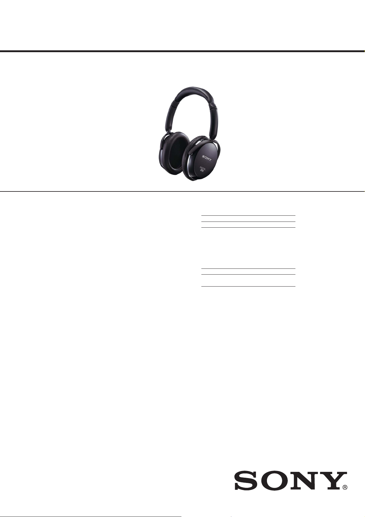
MDR-NC500D
SERVICE MANUAL
Ver. 1.2 2008.10
SPECIFICATIONS
General
Type Closed dynamic
Driver unit 40 mm, dome type (CCAW adopted)
Power handling capacity 100 mW
Impedance 40 Ω at 1 kHz
Sensitivity 102 dB/mW
Frequency response 5 - 24,000 Hz
Total Noise Suppression Ratio*1 Approx. 20 dB
Power source DC 3.7 V: Built-in lithium-ion
2 × LR6 (size AA) batteries,
or AC power adaptor
Mass Approx. 195 g (6.9 oz)
Supplied accessories
Connecting cord (0.5 m, gold plated stereo mini plug) (1)
Connecting cord (1.5 m, gold plated L type stereo mini plug) (1)
Connecting cord with battery case (1)
Carrying case (1)
Plug adaptor for in-fl ight use*3 (single/dual) (1)
Gold-plated unimatch plug adaptor
(stereo phone plug y stereo mini jack) (1)
Sony LR6 (size AA) batteries (2) (US and Tourist models)
AC power adaptor (1)
Operating Instructions (1)
Product Information (1)
Startup guide (1)
Card warranty (1)
*1
Under the Sony measurement standard.
For details about the Total Noise Suppression
Ratio amount for each mode, refer to the
Product Information booklet.
*2
Equivalent to approx. 99 % reduction of energy of sound compared
with not wearing headphones
(NC MODE A).
*3
May not be compatible with some in-fl ight music services.
rechargeable battery,
*2
US Model
Canadian Model
AEP Model
UK Model
E Model
Australian Model
Chinese Model
Tourist Model
General charging and usage time
Charging time Usage time
Approx. 3 hours *2 Approx. 15 hours
*1
At 1 kHz, 0.1 mW + 0.1 mW output
*2
Hours required to fully charge an empty battery
*3
Time stated above may vary, depending on ambient temperature or
conditions of use.
Battery life
Battery type Approx. hours
Sony Alkaline 10 hours
LR6 (size AA) battery
*1
Output at 1 kHz, 0.1 mW + 0.1 mW
*2
Time stated above may vary, depending on ambient temperature or
conditions of use.
Note (US and Tourist models)
Because the supplied battery was included in the package from the time of
manufacture (as a convenience to the user), it is possible that the battery
life may be somewhat depleted by the time of purchase. The actual life
of the supplied battery may be shorter than the standard time described in
this manual when using a fresh battery.
*1
*3
*1
*2
Design and specifi cations are subject to change without notice.
9-889-146-03
2008J05-1
2008.10
©
Sony Corporation
Audio&Video Business Group
Published by Sony Techno Create Corporation
NOISE CANCELING HEADPHONES
Page 2
MDR-NC500D
Ver. 1.2
NOTES ON CHIP COMPONENT REPLACEMENT
• Never reuse a disconnected chip component.
• Notice that the minus side of a tantalum capacitor may be damaged by heat.
Note
• Use the AC power adaptor supplied with this unit. Do
not use any other AC power adaptor since it may
cause the unit to malfunction.
Polarity of the plug
CAUTION
Danger of explosion if battery is incorrectly replaced.
Replace only with the same or equivalent type.
TABLE OF CONTENTS
1. SERVICING NOTES ............................................. 3
2. GENERAL .................................................................. 4
3. DISASSEMBLY
3-1. Disassembly Flow ........................................................... 5
3-2. MAIN Board (Rch) ......................................................... 6
3-3. Battery (Li-ion) Sub Assy (Lch) ..................................... 6
3-4. CHARGER Board (Lch) ................................................. 7
3-5. Wire Setting .................................................................... 8
4. ELECTRICAL ADJUSTMENT ........................... 9
5. DIAGRAMS
5-1. Block Diagram - AUDIO Section - ................................. 13
5-2. Block Diagram - POWER SUPPLY Section - ................ 14
5-3. Printed Wiring Board - MAIN Board - ........................... 16
5-4. Schematic Diagram - MAIN Board (1/3) - ..................... 17
5-5. Schematic Diagram - MAIN Board (2/3) - ..................... 18
5-6. Schematic Diagram - MAIN Board (3/3) - ..................... 19
5-7. Printed Wiring Board - CHARGER Board
(US, CND, JE models) - ................................................. 20
5-8. Printed Wiring Board - CHARGER Board
(Except US, CND, JE models) - ..................................... 20
5-9. Schematic Diagram - CHARGER Board - ..................... 21
SAFETY-RELATED COMPONET WARNING!
COMPONENTS IDENTIFIED BY MARK 0 OR DOTTED LINE
WITH MARK 0 ON THE SCHEMATIC DIAGRAMS AND IN
THE PARTS LIST ARE CRITICAL TO SAFE OPERATION.
REPLACE THESE COMPONENTS WITH SONY PARTS
WHOSE PART NUMBERS APPEAR AS SHOWN IN THIS
MANUAL OR IN SUPPLEMENTS PUBLISHED BY SONY.
ATTENTION AU COMPOSANT AYANT RAPPORT
À LA SÉCURITÉ!
LES COMPOSANTS IDENTIFIÉS PAR UNE MARQUE 0 SUR
LES DIAGRAMMES SCHÉMATIQUES ET LA LISTE DES
PIÈCES SONT CRITIQUES POUR LA SÉCURITÉ DE FONCTIONNEMENT. NE REMPLACER CES COMPOSANTS QUE
PAR DES PIÈCES SONY DONT LES NUMÉROS SONT DONNÉS DANS CE MANUEL OU DANS LES SUPPLÉMENTS
PUBLIÉS PAR SONY.
6. EXPLODED VIEWS
6-1. Housing, Lithium-Ion Battery Section ............................ 28
6-2. MAIN Board, CHARGER Board Section ...................... 29
7. ELECTRICAL PARTS LIST .............................. 30
Accessories are given in the last of the electrical parts list.
• Abbreviation
CND : Canadian model
JE : Tourist model
2
Page 3

SECTION 1
SERVICING NOTES
UNLEADED SOLDER
Boards requiring use of unleaded solder are printed with the leadfree mark (LF) indicating the solder contains no lead.
(Caution: Some printed circuit boards may not come printed with
the lead free mark due to their particular size)
: LEAD FREE MARK
Unleaded solder has the following characteristics.
• Unleaded solder melts at a temperature about 40 °C higher
than ordinary solder.
Ordinary soldering irons can be used but the iron tip has to be
applied to the solder joint for a slightly longer time.
Soldering irons using a temperature regulator should be set to
about 350 °C.
Caution: The printed pattern (copper foil) may peel away if
the heated tip is applied for too long, so be careful!
• Strong viscosity
Unleaded solder is more viscous (sticky, less prone to fl ow)
than ordinary solder so use caution not to let solder bridges
occur such as on IC pins, etc.
• Usable with ordinary solder
It is best to use only unleaded solder but unleaded solder may
also be added to ordinary solder.
MDR-NC500D
NOTE OF REPLACING THE IC501, IC551, IC601,
IC801 AND IC802 ON THE MAIN BOARD
IC501, IC551, IC601, IC801 and IC802 on the MAIN board cannot exchange with single. When these parts on the MAIN board are
damaged, exchange the entire mounted board.
NOTE OF REPLACING THE IC402 ON THE CHARGER
BOARD
IC402 on the CHARGER board cannot exchange with single.
When this part on the CHARGER board is damaged, exchange the
entire mounted board.
3
Page 4
MDR-NC500D
SECTION 2
GENERAL
This section is extracted
from instruction manual.
Features
(US and Tourist models )
• Digital noise canceling headphones
with Sony’s unique DNC Software
Engine.
Creation of a high-precision canceling signal
delivers outstanding noise canceling
performance.
• AI (Artificial Intelligence) Noise
Canceling function.
Automatic selection of the optimal noise
canceling mode based on intelligent analysis of
environmental ambient noise.
Digital equalizer delivers ideal frequency
•
response and high-quality music
reproduction.
• High S/N ratio achieved through digital
signal processing.
• Lightweight design creates extremely
comfortable wearing fit.
Generous use of lightweight materials such as
Magnesium and A7075 aluminum alloy.
• Pressure relieving urethane cushion in
the earpad.
The earpad structure provides comfort without
stress even after extended use.
• Built-in monitor function lets you
silence the audio to listen outside.
Features
(Except US and Tourist models )
•
Digital noise canceling headphones with
Sony’s unique DNC Software Engine.
Reduces approx. 99% of ambient noise by
creating a high-precision canceling signal.
• AI (Artificial Intelligence) Noise
Canceling function.
Automatic selection of the optimal noise
canceling mode based on intelligent analysis of
environmental ambient noise.
• Digital equalizer delivers ideal
frequency response and high-quality
music reproduction.
• High S/N ratio achieved through digital
signal processing.
• Lightweight design for extremely
comfortable wearing.
Generous use of lightweight materials such as
Magnesium and A7075 aluminum alloy.
• Pressure relieving urethane cushion in
the earpad.
The earpad structure provides comfort without
stress even after extended use.
• Built-in monitor function lets you
silence the audio to hear externally.
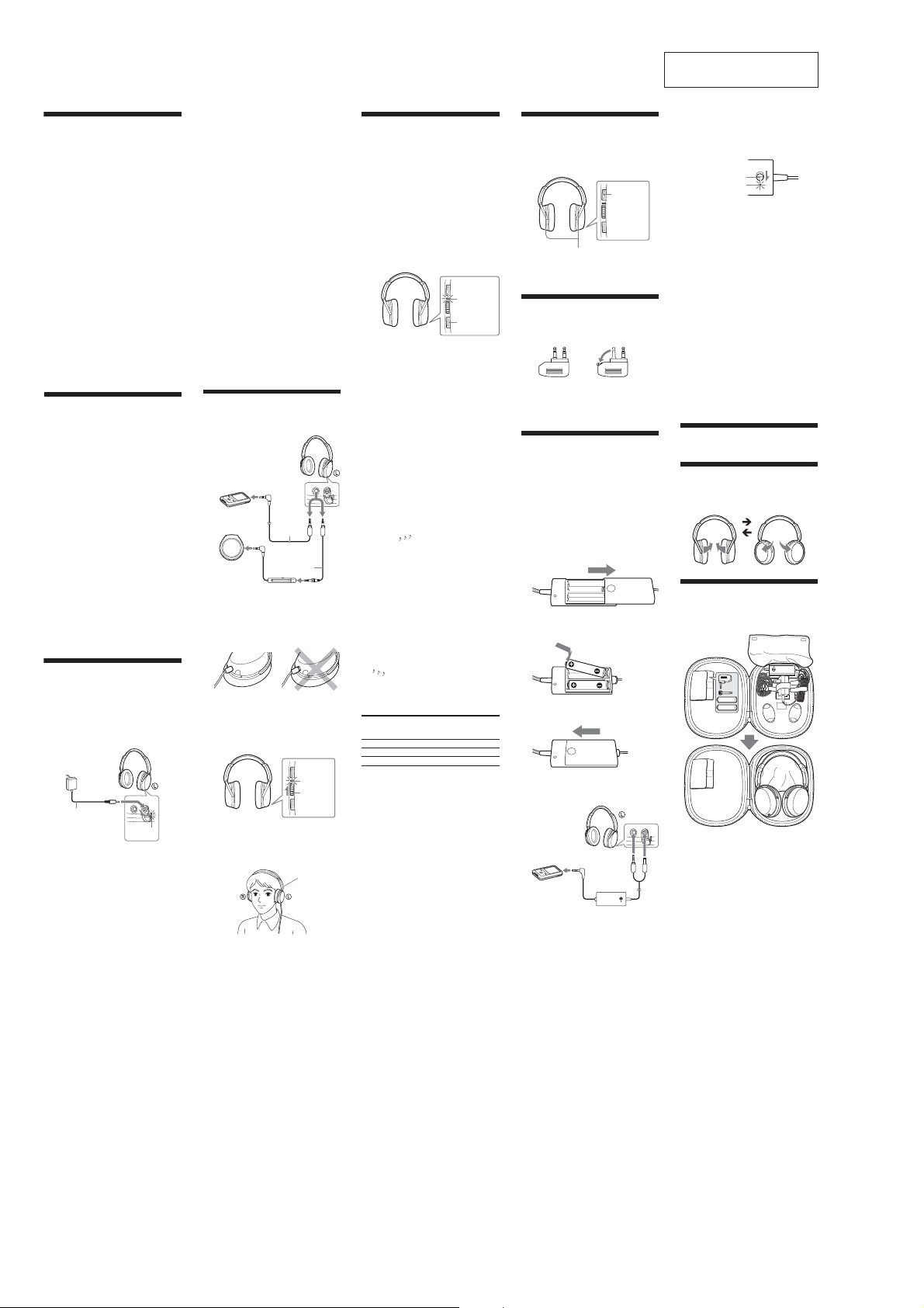
Charge the headphones
The headphones contains a rechargeable LithiumIon battery. Charge the battery before use.
Connect the supplied AC power adaptor to the DC
IN 6V jack on the headphones and an AC outlet.
The charge indicator lights up in orange and
charging starts.
To an AC outlet
AC power
To DC IN
adaptor
6V jack
(supplied)
Charging is completed after about three hours,
and the charge indicator goes out.
Disconnect the AC power adaptor after the
charging has finished.
Charge
indicator
Headphones
When the rechargeable
battery is low
When the rechargeable battery is low, short beeps
sound from the unit for 8 seconds and the
POWER indicator blinks slowly.
When the battery level is getting lower, a long
beep sounds from the unit for 2 seconds and the
POWER indicator blinks quickly, and all
operations are stopped. Move the POWER switch
to “OFF” in this case.
[Tips
When the battery runs out, you can supply the power to
the headphones in one of the following ways:
• Connect the headphones to the AC power adaptor by
following the steps shown in “Charge the
headphones.”
You can use the headphones while charging.
• Use the supplied connecting cord with battery case.
See “How to use the connecting cord with battery
case” for details.
Using your AC power
adaptor abroad
You can use yourAC power adaptor in any
country or area that uses 100 V to 240 VAC,
50/60 Hz, by connecting a plug adaptor. If the
country you visit employs a different shaped
socket, use the correct plug adaptor.
Consult your nearest travel bureau for the type of
plug adaptor needed for your trip.
Listening to music
1 Connect the headphones to the AV
equipment.
When connecting
to the stereo mini
jack of a
WALKMAN*, etc.
When connecting
to the stereo mini
jack of the remote
control supplied
with a WALKMAN,
etc.
* “WALKMAN” and “WALKMAN” logo are
registered trademarks of Sony Corporation.
Notes
• When connecting the cord, insert the plug into the
jack until the green portion of the plug disappears.
• To disconnect the cord, pull it out by the plug, not
the cord, as the inner conductors may break.
2 Turn on the power on the right side of the
headphones.
The POWER indicator lights up in blue, and a
short beep sounds from the unit.
3 Put on the headphones.
After confirming the cord on the left and the
POWER switch on the right, put on the
headphones.
Adjust the ear pads so as to cover your ears.
4 Start playing on the AV equipment
connected to the headphones.
Note
Playback is not available when there is no
power.
Headphones
Connecting
cord 1.5 m
(supplied)
Connecting cord
0.5 m (supplied)
Remote
control
3-
POWER
indicator
POWER
switch
Tactile dot
(on the left)
Utilizing the AI Noise
Canceling
1 Press the AI NC MODE button.
When you press the AI NC MODE
the POWER switch is set to “ON”, sounds
come from the headphones to inform you that
the unit has started analyzing ambient sound
components (approx. 3 seconds).
During analysis, sound reproduction from the
unit is stopped and the POWER indicator
lights in pink.
When analysis is completed, the most
effective noise canceling mode is set
automatically, and sound reproduction from
the headphones starts.
AI Noise Canceling
AI Noise Canceling is a useful function that
automatically selects one of the noise canceling
modes. This function provides the most effective
noise canceling mode by immediately analyzing
ambient sound components when the AI NC
MODE button is pressed.
[Tips
• When the power of the headphones is turned on,
mode A is set. (See “Noise canceling mode types,”
for details about Mode A.)
• Press the AI NC MODE button again to reset the
noise canceling mode if ambient noise has changed,
such as when you move outdoors from a room.
To set the noise canceling mode
manually
You can set the noise canceling mode manually
(manual noise canceling).
1 Press and hold the AI NC MODE button
for more than one second.
Sounds ( ) come from the headphones to
inform you that manual noise canceling is set.
2 Press the AI NC MODE button
repeatedly to change the mode type.
The POWER indicator blinks pink and a
beep(s) sound(s) from the headphones. After
that, the noise canceling mode is set. The
number of POWER indicator blinks and the
beep sounds depends on the mode selected.
See “Noise canceling mode types.”
[Tips
• Mode A is selected when manual noise canceling is
activated.
• To change from manual noise canceling to AI Noise
Canceling, press and hold the AI NC MODE button
for more than one second. When you hear the sounds
) to inform you of the change to AI Noise
(
Canceling, press the AI NC MODE button again.
Ambient analysis starts and the most effective noise
canceling mode is set automatically.
Noise canceling mode types
Mode names Number of POWER indicator
A1
B2
C3
A:Noise mainly in an airplane is effectively reduced.
B:Noise mainly in a bus or a train is effectively
reduced.
C:Noise mainly found in an office environment (PC,
copier, air ventilation, etc.) is effectively reduced.
blinks (pink) and beep
sounds
button
POWER
indicator
3-
AI NC MODE
button
Hearing environmental
sound for safety
If the MONITOR
the POWER switch is set to ON, playback silences
then you can hear the surrounding environment.
and
Note
Environmental sound might not be heard if the
microphone is covered with your fingers.
button
Monitor microphone
When using in an
airplane
• The supplied plug adaptor can be connected to
the dual or stereo mini jacks in an airplane.
for dual jacks for stereo mini jacks
• Do not use the headphones when use of
electronic equipment is prohibited, or when use
of personal headphones for in-flight music
services are prohibited.
How to use the
connecting cord with
the battery case
You can continue to use the unit, even when the
rechargeable battery in the headphones runs out,
by connecting the supplied connecting cord with
battery case.
Use the connecting cord with battery case by
inserting two size AA alkaline batteries.
1 Open the lid of the battery case.
2 Insert two size AA alkaline batteries.
Make sure of direction, matching the F
marks in the case with those on the batteries.
3 Close the lid.
4 Connect the supplied connecting cord
with the battery case to both the
headphones and AV equipment.
Headphones
AV equipment
Notes
• When connecting the cord, insert the plug fully into the
jack so that the green sign on the metal parts cannot be
seen.
• When disconnecting the cord, pull it out by holding the
plug. If the cord is pulled forcibly the wire may break.
is pressed and held while
MONITOR
button
3-
Connecting cord with
battery case (supplied)
5 Set the POWER switch of the
headphones to “OFF,” and then set the
POWER switch of the battery case to
“ON.”
The POWER indicator on the battery case
lights up green.
POWER switch
POWER indicator
See steps 2 to 4 of “Listening to music” for
the following setting steps.
After use, set the POWER switch of both the
headphones and the battery case to “OFF.”
[Tips
• The power supply of the rechargeable battery is
consumed first, unless the battery runs out.
• If you connect and turn on the connecting cord with
the battery case in advance when the rechargeable
battery is low, you can use the headphones
uninterrupted, even after the battery in the
headphones runs out.
Notes
• The use of manganese batteries is not recommended,
since this type of battery has an extremely short
usage time.
• The battery case supplies the power to the
headphones for operation purposes only. It does not
charge the internal rechargeable battery in the
headphones.
• The POWER indicator of the battery case becomes
dim when the battery life is reaching the limit.
Replace the battery with new ones at the time.
• The supplied connecting cord with battery case is
only for these headphones. Do not connect to other
equipment.
After use
Turn off the power of the headphones.
Flat Storage
he housings rotate to make them flat for easy
storage in the carrying case (supplied), or in a seat
pocket. Restore to their usual position before using.
3-3-
Putting the headphones
in the carrying case
Rotate the housings to be flat before putting them
in the carrying case.
T
4
Page 5
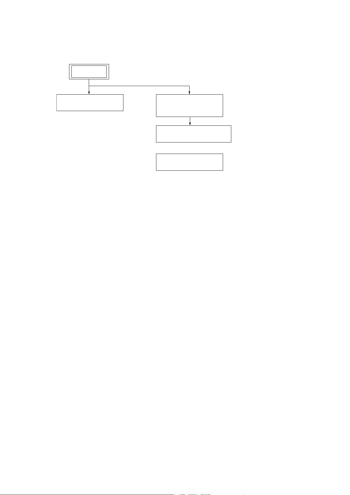
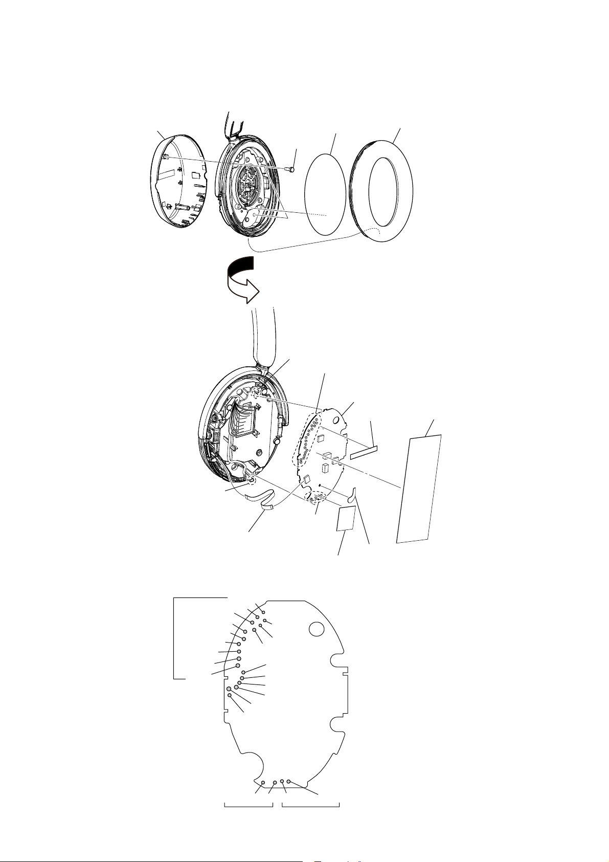
SECTION 3
DISASSEMBLY
• This set can be disassembled in the order shown below.
3-1. DISASSEMBLY FLOW
SET
– Rch – – Lch –
3-2. MAIN BOARD (Rch)
(Page 6)
3-3. BATTERY (LI-ION)
SUB ASSY (Lch)
(Page 7)
3-4. CHARGER BOARD (Lch)
(Page 8)
3-5. WIRE SETTING
(Page 8)
MDR-NC500D
5
Page 6
MDR-NC500D
Note: Follow the disassembly procedure in the numerical order given.
3-2. MAIN BOARD (Rch)
housing (R) sub assy
two screws
(M2.6)
screen
ear pad (R)
claw
RB
flexible flat cable
(MAIN board: CN405/POWER board)
• POSITION OF LEAD WIRES (MAIN board: Side B)
natural
red
red (SP201)
to CHARGER board
red/dark blue
dark blue
red/green
natural/green
green
white
black
claw
RB
Remove solders.
yellow
blue
natural
natural (MC201)
blue (MC201)
natural (MC201)
blue (MC231)
natural (SP201)
Remove solders.
RT
cushion saranet
MAIN board
sheet (A)
shield sheet (D)
shield sheet (C)
natural
to MODE board to RESET board
natural greenred
6
Page 7

3-3. BATTERY (LI-ION) SUB ASSY (Lch)
screen
ear pad (L)
shield sheet (B)
MDR-NC500D
battery (LI-ION) sub assy lead
CN403
black
two screws
(M2.6)
battery (LI-ION) sub assy
3-4. CHARGER BOARD (Lch)
connector
claw
claw
red
sheet (B)
housing (L) sub assy
CHARGER board
claw
• POSITION OF LEAD WIRES (CHARGER board)
– Side A – – Side B –
red/dark blue
to MAIN board
dark blue
black
green
natural/green
red/green
claw
Remove solders.
CHARGER board
flexible flat cable
(CHARGER board: CN402/JACK board)
blue
natural
yellow
natural
white
red
black (housing plate)
black (JACK board)
natural (MIC101)
blue (MIC131)
natural (MIC131)
to MAIN board
natural (SP101)
blue (MIC101)
red (SP101)
red (JACK board)
7
Page 8
MDR-NC500D
3-5. WIRE SETTING
– Lch – – Rch –
relay cord
MIC NC wireMIC NC wire
JACK wire
driver wiredriver wire
relay cord wire
sheet (A)
relay cord
MIC monitor wire
ground wire
JACK board
relay cord wire
flexible flat cable
sheet (B)
MODE board wire
RESET board wire
cushion saranet
8
Page 9
MDR-NC500D
SECTION 4
ELECTRICAL ADJUSTMENTS
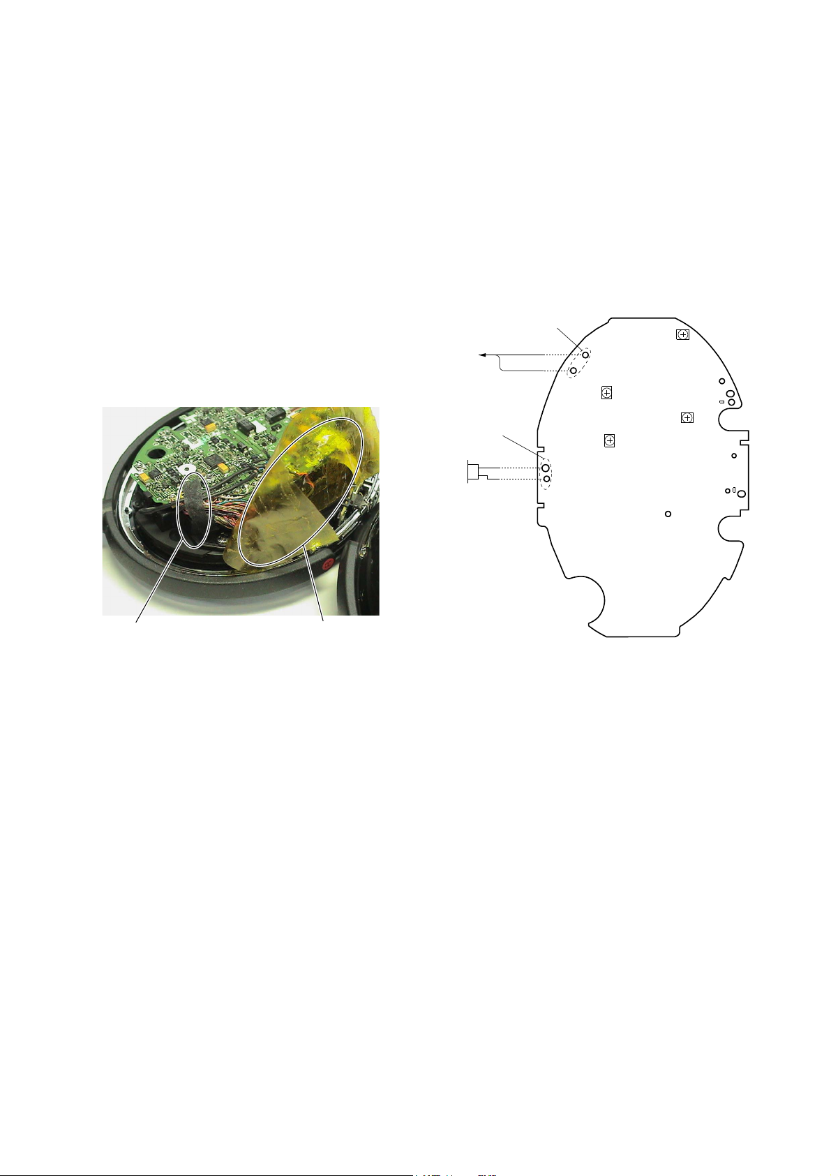
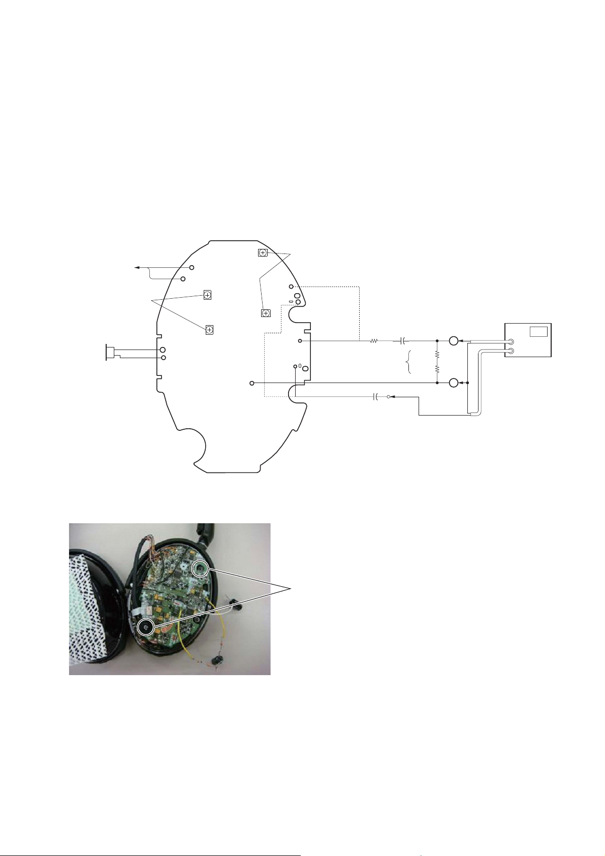
NOISE CANCELING VOLUME ADJUSTMENT
Procedure:
1. Prepare the following parts.
22 kΩ resistor (Part No.: 1-260-115-11)
330 Ω resistor (Part No.: 1-260-093-11)
270 Ω resistor (Part No.: 1-260-092-11)
39 Ω resistor (Part No.: 1-260-082-11)
100 µF capacitor (Part No.: 1-126-933-11)
2. Remove the shield sheet (C) and sheet (A). (Refer to Fig. 1-1)
3. Remove lead wires of the TP182 (dark blue), TP183 (red/dark blue). (for CHARGER board (SP101)) (Refer to Fig. 1-2)
4. Remove lead wires of the TP282 (natural), TP283 (red). (for SP201) (Refer to Fig. 1-2)
– MAIN Board (Side B) –
CHARGER board
(SP101)
Remove
Remove
Red/Dark Blue
Dark Blue
TP183
TP182
RV101
RV282
TP284
R211
RV182
SL201
TP203
RV201
TP282
TP283
remove the sheet (A) remove the shield sheet (C)
SP201
Natural
Red
Fig. 1-1 Fig. 1-2
TP478
TP184
TP103
R111
SL101
9
Page 10
MDR-NC500D
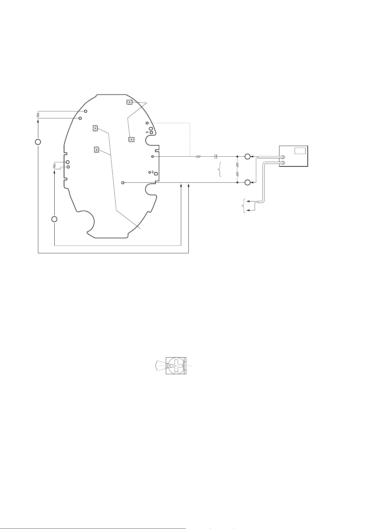
1 AMP Gain Adjustment
Connection:
1. Connect resistors (22 kΩ, 330 Ω + 270 Ω) and capacitor (100 µF) to the TP184, TP478. (Refer to Fig. 2)
2. Connect a resistor to (39 Ω) the TP182, TP183. (Refer to Fig. 2)
3. Connect a resistor to (39 Ω) the TP282, TP283. (Refer to Fig. 2)
– MAIN Board (Side B) –
39 Ω
level
C
(measure
L-CH)
39 Ω
level
D
(measure
R-CH)
RV282
TP183
TP182
RV101
RV182
RV201
TP282
TP283
TP478
TP284
R211
TP184
R111
TP103
Do not touch in
this adjustment.
adjustment parts
(input R-CH)
SL201
TP203
(input L-CH)
SL101
100 µF
22 kΩ
+
330 Ω
600 Ω
270 Ω
measure $(L-CH)
and %(R-CH) level
A
B
Fig. 2
Adjustment:
– L-CH –
1. Connect an audio analyzer (output impedance: 600 Ω) to A and B in Fig. 2.
2. Input the signal (1 kHz, 0 dBv) from the audio analyzer.
3. Adjust RV182 so that C level in Fig. 2 (between TP182 and TP478) is –2.6 dBv ± 0.1 dB. (Refer to Fig. 3)
audio analyzer
OUT
IN
output impedance: 600 Ω
signal: 1 kHz, 0 dBv
– R-CH –
4. Remove the one side of resistor (22 kΩ) of the TP184, and connect to TP284. (Refer to Fig. 3)
5. Input the signal (1 kHz, 0 dBv) from the audio analyzer.
6. Adjust RV282 so that the D level in Fig. 2 (between TP238 and TP478) is –2.6 dBv ± 0.1 dB. (Refer to Fig. 3)
15°
0°
–15°
RV182, RV282
nearby mechanical center
Fig. 3. Adjusted position (reference)
10
Page 11
MDR-NC500D
2 Canceling Gain Adjustment
Procedure:
1. Remove the resistors (39 Ω) from TP182, TP183.
2. Remove the resistors (39 Ω) from TP282, TP283.
3. Connect the lead wires of CHARGER board (SP101) to the TP182 (dark blue), TP183 (red/dark blue). (Refer to Fig. 4)
4. Connect the lead wires of SP201 to the TP282 (natural), TP283 (red). (Refer to Fig. 4)
5. Remove the one side of resistor (22 kΩ) of TP284, and connect to TP184. (Refer to Fig. 4)
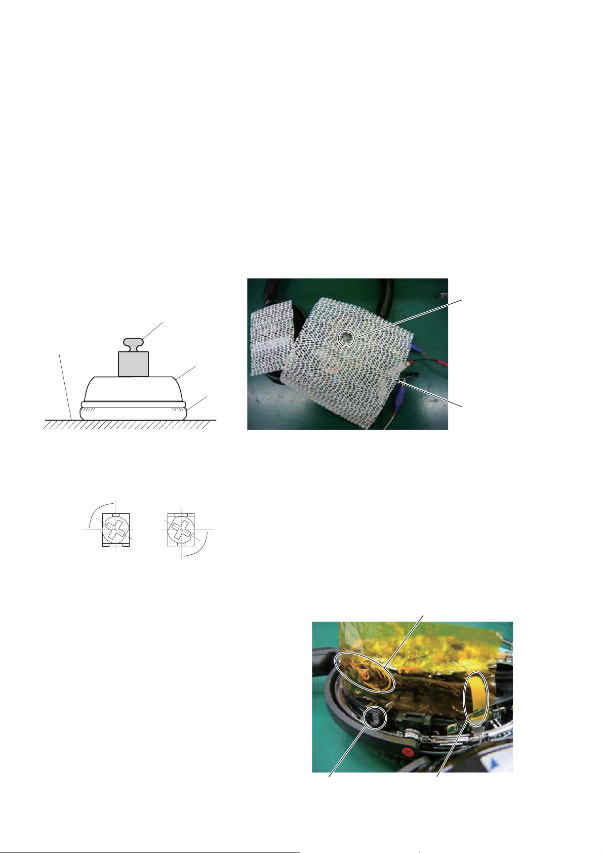
6. The screw is closes into the hole (two places) where housing (R-CH side) is fi xed. It closes it so that air should not leak. (Refer to Fig.
5)
Note: The problem is not in this hole even if it closes it with not the screw but clay, tape and so on. The hole is completely closed with stability so as not to
do the air leak.
7. Remove the R111 (0 Ω) and R211 (0 Ω).
8. Connect a capacitor (100 µF) to the TP103.
– MAIN Board (Side B) –
CHARGER board
(SP101)
adjustment parts
SP201
Red/
Dark Blue
Dark Blue
Natural
Red
TP282
TP283
TP183
TP182
RV101
RV201
RV282
TP284
R211
RV182
TP184
TP103
TP478
(measure R-CH)
Do not touch in
this adjustment.
(input R-CH)
SL201
TP203
(input L-CH)
R111
SL101
(measure L-CH)
Fig. 4
22 kΩ
+
100 µF
100 µF
600 Ω
+
330 Ω
270 Ω
audio analyzer
A
B
OUT
IN
output impedance: 600 Ω
signal: 220 Hz, –26 dBv
Fig. 5
hole for R-CH side housing fixation
(completely closes it with screw,
clay, tape and so on)
11
Page 12
MDR-NC500D
Adjustment:
– L-CH –
1. Put the housing (L-CH side) on fl at table.
2. Put a weight (500 g) on the housing. (Refer to Fig. 6)
3. Press the housing so that the fl at table of ear pad is sealed. (It notes do not press very strong)
4. Input the signal (220 Hz, –25 dBv) from the audio analyzer.
5. Adjust RV101 so that the level of connected capacitor to TP103 is –14 dBv ± 0.3 dB. (Refer to Fig. 8)
– R-CH –
6. Remove the one side of resistor (22 kΩ) of the TP184, and connect to TP284.
7. Remove the one side of capacitor (100 µF) of the TP103, and connect to TP203
8. Put the housing (R-CH side) on fl at table.
9. Put a weight (500 g) on the housing. (Refer to Fig. 6)
(MAIN board is covered so that there is no short-circuit. RV201 makes it not blocked with the cover) (Refer to Fig. 7)
10. Press the housing so that the fl at table of ear pad is sealed. (It notes do not press very strong)
11. Input the signal (220 Hz, –25 dBv) from the audio analyzer.
12. Adjust RV201 so that the level of connected capacitor to TP203 is –14 dBv ± 0.3 dB. (Refer to Fig. 8)
weight (500g)
hole (RV201)
flat table
housing
ear pad
Fig. 6 Fig. 7
90°
nearby 30°
0°
RV101
90°
RV201
0°
nearby 30°
Fig. 8. Adjusted position (reference)
End of adjustment processing:
lead wires are stored on the MAIN board side
1. Remove the resistors (22 kΩ, 330 Ω + 270 Ω) and capacitor
(100 µF) from TP284, TP478.
2. Remove the capacitor (100 µF) from TP203.
3. SL101 and SL201 are short-circuited with solders.
4. The screw (or clay, tape and so on) fi xed to the hole is re-
moved.
5. Wire setting, shield sheet (C) and sheet (A) are pasted.
(Flexible fl at cable is cover. MIC is not cover) (Refer to Fig.
9)
cover
12
MIC is not cover flexible flat cable is cover
Fig. 9
Page 13

5-1. BLOCK DIAGRAM - AUDIO Section -
JACK BOARD (1/3)
(INPUT)
LINE AMP
IC361 (1/2)
LINE AMP
IC361 (2/2)
SECTION 5
DIAGRAMS
STEREO AUDIO CODEC
17 LLINEIN
16
RLINEIN
STEREO AUDIO CODEC
17 LLINEIN
16
RLINEIN
X501
12.288MHz
23 XTO
22 XTI/MCLK
IC551
3
DOUT A10 A11DR2 DX2
28BCLK A9 CLKR2
4LRCOUT C9 FSR2
22
XTI/MCLK
SDIN
SCLK
22
21
IC501 (1/2)
3
DOUT
28BCLK
4LRCOUT
27
CLKOUT
SDIN
SCLK
22
21
D8 DR1
D7 CLKR1
B10 CLKX2
A7 FSR1
D10 F S X 2
F2 X2/CLKIN
DSP
IC601
D6DR0 35
E7DX0
B5CLKR0 37
C6CLKX0
A5FSR0 50
B6FSX0 49
G14_INT0 2
G13_INT1 1
A3GPIO4 29
D5GPIO5 27
H12_RESET 32
STEREO AUDIO CODEC
IC501 (2/2)
1DIN
SYSTEM CONTROLLER
IC801 (1/2)
DR0
36 DX0
CLK0
FSR0
FSX0
INT0
INT1
GPIO4
GPIO5
DSPRST
15 SDA
14 SCLK
MDR-NC500D
RV182
AMP GAIN
9LOUT
10ROUT
3AMUTE
19MO NPATH
21HYBPATH1
20HYBPATH2
+
POWER AMP
IC184
SIGNAL PATH
SP101
(L-CH)
: AUDIO (ANALOG)
: AUDIO (DIGITAL)
: MONITOR
MIC131
(MONITOR)
MIC101
(NOISE DETECT)
MIC231
(MONITOR)
MIC201
(NOISE DETECT)
MIC BIAS
Q130
MIC BIAS
Q230
A+3.3V
A+3.3V
MIC AMP
IC301 (1/2)
RV101
CANCELING GAIN
MIC AMP
IC301 (2/2)
RV201
CANCELING GAIN
AUDIO SWITCH
IC183
AUDIO SWITCH
IC181
AUDIO SWITCH
IC182
AUDIO SWITCH
IC283
AUDIO SWITCH
IC281
AUDIO SWITCH
IC282
RV282
AMP GAIN
+
POWER AMP
IC284
AMP OFF
SWITCH
Q476
SP201
(R-CH)
SD
A
MDR-NC500D
1313
Page 14

MDR-NC500D
5-2. BLOCK DIAGRAM - POWER SUPPLY Section -
POWER BOARD (1/2)
(POWER)
(AI NC MODE)
LED DRIVE
Q802
LED DRIVE
Q801
SYSTEM CONTROLLER
IC801 (2/2)
30 LED_R
POWER BOARD (2/2)
SD
A
MONITOR
24KEYMON
40VBATT
D802
4DDCE
25KEYMODE
POWER
ON 5 OFF
MODE BOARD
AI NC MODE
RESET BOARD
D+2.1V
A+3.3V
SWITCHING
Q474 (1/2)
DC/DC CONVERTER
IC472
4
SW1
6
SW2
RUN1
RUN2
2
7
3Vin
POWER/CHARGE CONTROL
IC402
15
OUT
16
OUT
17
12TS9
5BAT2618 KEYPOWERLED_B OUT
6BAT
4IN
7ISET2
MODE
8
2STAT1
CE
JACK BOARD (2/3)
(CHARGE)
DC/DC
CONVERTER
IC401, Q401
BATT101
LITHIUM ION
BATTERY
3.7V 1,260mAh
RESET
SWITCH
Q404
SWITCH
Q403
Q402
D+1.35V
D+2.8V
RESET SIGNAL
GENERATOR
IC802
SWITCHING
Q474 (2/2)
DC/DC CONVERTER
IC473
4
SW1
6
SW2
RUN1
RUN2
2
7
3Vin
B+ SWITCH
Q472, 473
VOLTAGE
DETECT
IC471
5_RESET
Q475
VOLTAGE
DETECT
IC403
VOLTAGE
DETECT
IC404
VOLTAGE
DETECT
IC405
JACK BOARD (3/3)
−
+
DC IN 6V
TH401
6BATTSEL
SWITCHING
Q405
MDR-NC500D
1414
Page 15

MDR-NC500D
THIS NOTE IS COMMON FOR PRINTED WIRING BOARDS AND SCHEMATIC DIAGRAMS.
(In addition to this, the necessary note is printed in each block.)
For Printed Wiring Boards.
Note:
• Y : parts extracted from the conductor side.
• : Pattern from the side which enables seeing.
(The other layers' patterns are not indicated.)
Caution:
Pattern face side:
(SIDE B)
Parts face side:
(SIDE A)
• MAIN board is multi-layer printed board. However, the
patterns of intermediate-layers have not been included in
diagrams.
• Lead layouts
Parts on the pattern face side seen from
the pattern face are indicated.
Parts on the parts face side seen from
the parts face are indicated.
surface
CSP (Chip Size Package) Lead layout of conventional IC
For Schematic Diagrams.
Note:
• All capacitors are in µF unless otherwise noted. (p: pF) 50
WV or less are not indicated except for electrolytics and
tantalums.
• All resistors are in Ω and 1/4 W or less unless otherwise
specifi ed.
• A : B+ Line.
• H : adjustment for repair.
• Power voltage is dc 3.7 V and fed with regulated dc power
supply from CN403 pin 1 and pin 2 on the CHARGER
board.
• Voltages and waveforms are dc with respect to ground
under no-signal conditions.
no mark : POWER ON
• Voltages are taken with VOM (Input impedance 10 MΩ).
Voltage variations may be noted due to normal production
tolerances.
• Waveforms are taken with a oscilloscope.
Voltage variations may be noted due to normal production
tolerances.
• Circled numbers refer to waveforms.
• Signal path.
F : AUDIO (ANALOG)
J : AUDIO (DIGITAL)
N : MONITOR
• The voltage and waveform of CSP (chip size package)
cannot be measured, because its lead layout is different
from that of conventional IC.
• Abbreviation
CND : Canadian model
JE : Tourist model
• Circuit Boards Location
– Rch –
MAIN board
RESET board
POWER board
MODE board
– Lch –
CHARGER board
JACK board
• Waveforms
– MAIN Board –
IC472 (SW1)
472 ns
200 mV/DIV, 200 ns/DIV
IC472 (SW2)
468 ns
200 mV/DIV, 200 ns/DIV
0.5 Vp-p
0.6 Vp-p
IC473 (SW1)
IC473 (SW2)
468 ns
0.7 Vp-p
200 mV/DIV, 200 ns/DIV
0.7 Vp-p
472 ns
500 mV/DIV, 200 ns/DIV
IC501 XE (XTO)
81.5 ns
0.2 Vp-p
100 mV/DIV, 50 ns/DIV
MDR-NC500D
1515
Page 16

MDR-NC500D
5-3. PRINTED WIRING BOARD - MAIN Board -
• Semiconductor
Location
Ref. No. Location
D101 B-7
D102 C-7
D103 B-8
D104 B-8
D131 B-8
D132 B-8
D133 B-9
D134 B-9
D162 F-9
D163 F-9
D164 F-9
D165 F-9
D201 C-7
D202 C-8
D203 D-7
D204 D-8
D231 D-9
D232 D-8
D233 C-9
D234 C-9
D262 F-10
D263 F-10
D264 F-10
D265 F-10
D801 D-2
D802 D-3
IC181 D-10
IC182 D-10
IC183 D-9
IC184 D-10
IC281 C-9
IC282 B-9
IC283 A-8
IC284 A-9
IC301 C-8
IC361 E-10
IC471 D-8
IC472 F-8
IC473 E-7
IC501 C-5
IC551 B-4
IC601 E-3
IC801 C-2
IC802 C-3
Q130 B-8
Q230 D-8
Q472 E-8
Q473 E-8
Q474 G-8
Q475 G-9
Q476 D-8
Q801 C-2
Q802 B-2
A
B
C
D
E
F
12345678910
MAIN BOARD (SIDE A)
R813
R814
R815
C809
R818
G
• See Page 15 for Circuit Boards Location.
(NC)
CN801
TP832
TP807
C806
C807
R807
R837
Q801
C814
C810
R809
C815
R811
R812
R810
FB810
FB811
C808
D801
TP833
R817
R819
TP838
R629
C672
R640
R621
FB621
R644
R615
C665
C610
C615
C605
C604
C817
C626
R641
C816
C674
R626
C620
C673
R636
C621
R824
R635
R634
R639
R638
R808
R628
C611
C656
R805
TP839
R631
R632
R627
R630
C612
TP805
R806
C640
R637
C613
R610
FB601
TP803
C812
Q802
IC801
C642
C643
P14
N14
C633
M14
L14
K14
J14
C671
H14
G14
F14
E14
D14
C14
B14
A14
R604
R606
C647
P13
N13
M13
L13
K13
J13
H13
G13
F13
E13
D13
C13
B13
A13
R605
TP804
C636
P12
N12
M12
L12
K12
J12
H12
G12
F12
E12
D12
C12
B12
A12
R603
R642
10
L801
FB812
N11
M11
H11
G11
D11
C11
C645
FB813
R820
C635
P11
L11
K11
J11
F11
E11
B11
A11
TP802
TP808
C631
C641
P10
N10
M10
L10
K10
J10
H10
G10
F10
E10
D10
C10
B10
A10
C608
R804
R821
P9
N9
M9
L9
K9
IC601
E9
D9
C9
B9
A9
C603
C818
C625
R803
P8
N8
M8
L8
K8
E8
D8
C8
B8
A8
R643
TP801
SL801
C823
R838
C639
C650
TP809
TP806
SL803
SL802
R836
C822
C821
R834
C803
C802
R833
C820
C801
R832
R801
R827
R826
C819
R840
C638
P7
N7
M7
L7
K7
E7
D7
C7
B7
A7
P6
N6
M6
L6
K6
E6
D6
C6
B6
A6
C607
C623
R607
C813
P5
N5
M5
L5
K5
J5
H5
G5
F5
E5
D5
C5
B5
A5
C602
C637
R602
R828
C629
C634
P4
P3
P2
N4
N3
N2
M4
M3
M2
L4
L3
L2
K4
K3
K2
J4
J3
J2
H4
H3
H2
G4
G3
G2
F4
F3
F2
E4
E3
E2
D4
D3
D2
C4
C3
C2
B4
B3
B2
A4
A3
A2
C657
C601
C658
R608
L601
K
C630
R830
R829
R823
P1
N1
M1
R601
L1
K1
J1
H1
G1
F1
E1
D1
C1
B1
A1
C628
C606
R611
C554
R600
A
C652
R618
L551
K
R822
C614
R609
C648
R273
R173
R624
C617
C616
C558
R555
C551
IC802
R835
D802
C632
C627
C624
C622
C670
C663
R613
R614
C644
C661
TP834
• : Uses unleaded solder.
C560
C557
R557
R556
C552
L552
R616
R620
C646
C659
1-875-098-
15
21
TP473
C512
R612
R617
TP613
R619
C664
C669
C559
14
8
IC551
7
FB553
FB551
R560
TP552
R551
C508
14
22 28
C503
TP835
C511
C506
C502
R553
R554
TP553
TP551
C510
8
L502
1
28
22
C556
C553
FB552
C555
C509
TP505
R212
15
R112
R507
R506
21
X501
R509
C501
L501
C513
C504
R633
C649
L602
C651
12
(12)
TP504
IC501
FB503
7
TP502
1
FB504
R510
C505
FB501
TP506
R504
FB502
R501
TP501
TP503
R502
MAIN BOARD (SIDE B)
CHARGER
A1
BOARD
(US, CND, JE) (EXCEPT US, CND, JE)
R503
(Page 20) (Page 20)
MIC201
NOISE DETECT
(R-CH)
MIC231
MONITOR
(R-CH)
SP201
(R-CH)
HOUSING
PLATE
NATURAL
RED
CHARGER
A2
BOARD
RED/DARK BLU
NATURAL/GRN
POWER
BOARD
TP282
TP830
NATURAL
RED
BLU
NATURAL
DARK BLU
GRN
WHT
BLK
NATURAL
BLU
NATURAL
BLU
TP283
TP814
TP817
YEL
FB231
RED/GRN
TP361
TP161
TP471
TP472
C231
R487
C487
R488
TP811
TP201
TP231
R470
FB161
TP202
TP232
C497
TP815
TP261
FB361
L474
CN405
FB261
FB472
R496
D102
C470
FB202
C489
TP827
TP182
D101
C234
FB471
FB232
FB201
C201
TP476
C488
5
IC473
8
TP102
D201
D203
TP816
C104
R108
TP837
TP183
D104
D103
C202
C496
C485
TP475
R499
R494
C232
R201
1
FB102
R106
C490
4
D202
BLK
TP477
R486
R480
R207
D204
R286
R276
C291
TP132
TP101
R107
R105
R104
C302
FB132
TP131
FB101
R102
C301
C292
IC283
FB131
C102
R131
R103
C103
RV101
R101
C133
R298
4
C130
Q130
C132
R132
IC301
R203
R202
RV201
TP238
R478
R495
C478
Q473
C483
R208
C486
R479
R843
R206
R230
Q230
Q476
R457
C492
R484
C482
8
1
L471
MODE
BOARD
C476
R485
L472
R205
5
TP812
C204
C233
R235
R231
C230
IC471
R471
Q472
C495
4
C477
R477
TP474
IC472
C203
L473
C484
TP813
NATURAL NATURAL
FB282
C134
R233
13
5
R133
TP479
C480
R481
C494
TP826
2
R472
R232
D
R130
1
R288
R236
3
S
G
C475
R490
C288
R287
C287
D132
C135
R136
C235
C472
4
6
R492
TP810
RESET
BOARD
R259
C479
C481
Q474
D134
R137
R135
R237
FB283
D131
R238
FB182
C499
GRNRED
C284
IC284
D133
C283
R140
TP333
TP233
R240
D231D232
C471
C474
R482
R491
3
1
R493
C285
C282
R842
C498
TP281
3
R138
Q475
R284
R285
R282
R292
C289
1
IC282
54
C281
TP133
D233
FB183
IC183
TP162
TP478
R169
R174
D165
R162
R262
R261
R469
1-875-098-
R289
C294
R279
C290
4
5
IC281
RV182
D234
TP181
C192
R176
C183
R161
R290
R168
RV282
R171
R167
C163
C191
3
R166
C161
C261
3
1
C186
C164
(12)
R283
C286
R294
R177
D164
12
R198
R278
R186
54
C184
1
R164
TP290
R297
R213
R159
R188
R190
IC361
C162
R163
D162
D163
R172
R263
R280
R183
IC184
C185
C188
R182
R192
C194
C363
C264
R272
C262
R267
C263
D264
D265
R281
R184
R271
R264
R277
R296
R189
R187
TP289
R293
R180
R196
C187
C189
R179
IC182
TP262
C362
R266
R269
TP204
R185
TP190
R381
1
3
TP284
R211
TP189
TP103
R274
R268
SL201
TP203
IC181
R181
R193
4
5
C181
5
4
C361
D263
D262
TP184
C182
TP104
R111
3
1
R178
R194
R197
R113
SL101
C190
MDR-NC500D
Note: IC501, IC551, IC601, IC801 and IC802 on the MAIN board cannot exchange with single. When these parts on
the MAIN board are damaged, exchange the entire mounted board.
1616
Page 17

MDR-NC500D
5-4. SCHEMATIC DIAGRAM - MAIN Board (1/3) -
FB472
FB471
XC61GN3002HR
R479
330k
(1/3)
0
C472
0
0.1
C471
100
IC471
C478
10V
R472
470k
Q476
2SD2654
AMP
OFF SWITCH
Q473
2SC2712L
R495
100k
R494
33p
C499
0.01
47k
R480
330k
L471
4.7µH
C494
10
R492
Q474
SCH2401
SWITCHING
R496
0
(Page 21)
TP182
TP183
TP131
TP132
TP101
TP102
TP837
TP161
TP261
TP361
TP471
TP472
D/U(+)
D/U(-)
MIC(FF) SIG
MIC(FF) GND
MIC(FB) SIG
MIC(FB) GND
U-COM
SOUND(L)
SOUND(R)
SOUND(GND)
VDD
GND
C474
100
10V
TP479
TP478
2200p
C470
C475
0.1
C476 C477
47
10V
DTC115TE
INVERTER
R478
220k
R490
470k
Q475
0.01
R485 C486
750k 33p
• See Page 15 for Waveforms. • See Page 22 for IC Block Diagrams.
FB182
0
FB183
0
FB131
0
FB132
0
FB101
0
FB102
0
FB161
FB261
FB361
R471
10k
VOLTAGE
DETECT
R457 R477
1M 220k
DC/DC CONVERTER
IC472
LTC3547B
100
TP473
S
Q472
CPH3303
C482
22
10V
DC/DC CONVERTER
L472
4.7µH
Q472,473
B+ SWITCH
R499
0
TP474
C479R481
33p150k
C495
C480
R482
10
33k
C483
0.01
R491
100
C481
22
0.01
10V
TP475
C102
0.1
R262
1k
R261R161
R102R101 R103
10k2.7k 3.9k
C103
2.2
RV101
CANCELING GAIN
3939
C104
10p
RV101
47k
C261
0.15
R263
0
R271
4.7k
1SS380 1SS380
1SS380
C263
330p
R274R162
22k1k
R264
22k
1SS380 1SS380
C262
0.01
C264
0.1
LINE AMP
IC361
NJM2734
R277
100
D101 D102
1SS380 1SS380
R106
1k
D103 D104
LINE AMP
D262
D264 D265
C363
0.1
R107
22k
IC301
NJM2734
1SS380
R267
R105
A01
D162 D163
D263
R266
0
1k
TP262
R131
2.7k
0
R108
0
C161
R268
0.15
4.7k
R164
R269
0
R272
Q130
2SD2654
MIC BIAS
C132
0.1
22k
R163
0
C162
0.01
4.7k
TP162
R130
47k
C133
2.2
C130
4.7
10V
C301
0.1
1SS380 1SS380
C163 R167
330p 1k
R174
22k
D164 D165
1SS380 1SS380
C362C361 C164
10
0.1 0.1
10V
R172
4.7k
D131 D132
R133
1SS380 1SS380
4.7k
C135
R136
10p 1k
R140
0
10k
R132
C134
D133 D134
0.1
1SS380 1SS380
C234
0.1
C302
10
10V
R166
0
R168
4.7k
R169
0
4.7k
R171
R177
100
R135
0
R137
10k
R138
0
TP203
TP103
SL101
SL201
A02
A03
A04
A05
A06
A07
0
R111
A08
TP104
TP204
A09
R211
0
(Page 18)
A10
MDR-NC500D
MIC201
NOISE DETECT
(R-CH)
MIC231
MONITOR
(R-CH)
HOUSING
PLATE
TP201
TP202
TP231
TP232
TP238
C484 C485 R484
47
0.01 750k
10V
R486
470k
L473
4.7µH
C496 R470
10 0
FB232
FB201
FB202
FB231
R487 C487
C489
750k 33p
L474
4.7µH
IC473
LTC3547B
0
C201
0
4700p
0
C231
0
4700p
C497
R488
200k
10
C490
22
10V
TP477
TP476
0.01
D201 D202
R203R202
3.9k10k
C204
10p
1SS380 1SS380
R206
1k
RV201
47k
D203 D204
1SS380 1SS380
C233
0
RV201
CANCELING GAIN
0
2.2
R205
R207
22k
R208
C488
22
10V
C492
0.01
R469
100k
R493
10k
C498
0.1
R201
2.7k
C203
2.2
C202
0.1
R232 R233 R235
10k 4.7k 0
R231
2.7k
Q230
2SD2654
MIC BIAS
C232
0.1
R230
47k
C230
4.7
10V
D231 D232
1SS380 1SS380
C235 R236
10p 1k
R240
0
D233 D234
1SS380 1SS380
R237
10k
R238
0
TP133
TP233
TP333
A11
A12
A13
A14
A15
A16
A17
D-GND
DSP-GND
D-2.8V
D-1.35V
LI-ION
LCHV+
DD_CE
(Page 19)
1717
Page 18

MDR-NC500D
5-5. SCHEMATIC DIAGRAM - MAIN Board (2/3) -
(2/3)
A01
(Page
17)
A02
A03
A04
A05
A06
A07
A08
A10
A09
A11
A12
A13
A14
A15
A16
A17
R173
STEREO AUDIO
TLV320AIC23B
STEREO AUDIO
CODEC
IC501
TLV320AIC23B
R273
0
0
CODEC
IC551
SCLK
R555
0
MCK
SCLK
R509
1k
X501
12.288MHz
C512 C513
27p 27p
SDA
R556
10k
C553
0.1
C552 C555 FB552
10
10V
L551
10µH
R113
R112
SDA
0
R506 R507
10k 10k
0.1
C503
10V
10
H
C502
µ
10
L501
C501
0.1
• See Page 15 for Waveforms. • See Page 22 for IC Block Diagrams.
C557
0.1
C558
10
10k
10V
R557
C556
0.1
10
10V
L552
R560
10µH
10k
R551
220
TP552
C554C551
0.10.1
BCK2
0
0
R213
R212
0
C508
0.1
C509
10
10V
0.1
C506
FB502 FB503
00
FB504
FB501
10V
10
C505
0.1
C504
220
R510
TP506
H
µ
10
L502
220
R501
BCK
MCK
R503 R504
100 22
TP502
TP503
TP501
R502
0
DX2
0.1
C559
C560
10
10V
C181
0.1
HYB_MIX
C182
0.1
FB553
0
R554
0
0
100
FB551
R553
TP553
TP551
DR2
LRCK2
TP505
C510
0.1
C511
10
10V
TP504
DR1
LRCK
FF_MIX
MON_MIX
HYB_MIX
FF_MIX
MON_MIX
C183
0.1
C281
0.1
C282
0.1
C283
0.1
IC181
TC7SB66FU
IC183
TC7SB66FU
AUDIO SWITCH
VCC
AUDIO SWITCH
VCC
IC182
TC7SB66FU
VCC
VCC
TC7SB66FU
VCC
IC282
TC7SB66FU
AUDIO SWITCH
VCC
IC283
TC7SB66FU
AUDIO SWITCH
TP189 TP190
GND
GND
GND
GND
IC281
GND
GND
R196
0
R178
1M
C190
2200p
C194
33000p
R179
1M
R176 C191 R186
4.7k 0.22 22k
R198
1M
C192
0.01
R278
1M
C290
2200p
TP289
C294
33000p
R279
1M
R298
1M
C292
0.01
R181
R193
22k
R197 R194 R180
330k 0 33k
R192
12k
AUDIO SWITCH
AUDIO SWITCH
R182 R190
12k 0
C189
47000p
TP290
R296 R281
0 22k
R292 R282 R290
12k 12k 0
C289
47000p
C291 R286R276
0.22 22k4.7k
C186
2200p
R183
4.7k
TP184
0
C187
0.1
C287
0.1
R184
6.8k
TP181
10V
0.1
10
C185
C184
VDD
GND
R187
10k
22k
R188
R159
4.7k
TP284
R293R280R294R297
033k0330k
C284
C285
10
10V
R287
10k
C188
2200p
R285
10k
R283
C286
4.7k
R284
6.8k
2200p
2200p
RV282
22k
VDD
GND
R288
22k
C288
TP281
TLV4113
IC284
0.1
R259
4.7k
R185
10k
RV182 RV182
22k
2SD
1SD
R189
22k
R381
100k
2SD
1SD
R289
22k
AMUTE
AMP GAIN
POWER AMP
TLV4113
IC184
RV282
AMP GAIN
POWER AMP
FB282
FB283
MCK
BCK
LRCK
BCK2
LRCK2
DR1
DR2
DX2
SDA
SCLK
AMUTE
HYB_MIX
FF_MIX
MON_MIX
0
0
TP282
TP283
MCK
BCK
LRCK
BCK2
LRCK2
DR1
DR2
DX2
SDA
SCLK
AMUTE
HYB_MIX
FF_MIX
MON_MIX
(R-CH)
(Page
19)
SP201
MDR-NC500D
Note: IC501 and IC551 on the MAIN board cannot exchange with single. When these parts on the MAIN board are
damaged, exchange the entire mounted board.
1818
Page 19

MDR-NC500D
5-6. SCHEMATIC DIAGRAM - MAIN Board (3/3) -
(3/3)
MCK
HYB_MIX
MON_MIX
DSP-GND
D-GND
D-2.8V
D-1.35V
Li-ion
Lch V+
DDconCE
AMUTE
FF_MIX
LRCK2
BCK
LRCK
BCK2
DR1
DR2
DX2
SDA
SCLK
C633
0.1
C634
0.1
C635
0.1
C636
0.1
C637
0.1
C638
0.1
C639
0.1
C640
0.1
C641
0.1
C642
0.1
C643
0.1
C651
100
10V
C644
10
6.3V
C645
10
10V
C650
100
10V
C646
0.1
C647
L601
L602
0.1
10µH
C648
0.1
C649
0.1
C652
10µH
100p
R600 R601
1k 0
GPIO4
TP834
TP835
0.1
0.1
0.1
C603
C602
C601
R602 R603
00
BCK2
FSR0
LRCK
BCK
DR1
DR2
DX2
SDA
(Page
18)
(Page
17)
HYB_MIX
MON_MIX
DSP-GND
AMUTE
FF_MIX
D-1.35V
LRCK2
D-GND
D-2.8V
LCHV+
DD_CE
MCK
LRCK
BCK2
SCLK
LI-ION
• See page 23 for IC Pin Function Description.
C673
1000p
C674C632
1000p0.1
R632
1k
10k
0
0
R606
R604
FB601
C656
1000p
R605
100
DX2
DR2
C631
0.1
R631
1k
DSP
IC601 FB812
TMS320VC5503ZHH 0
CSP
(Chip Size Package)
R607
0.1
C657
C604
1000p
C605
C606
R608
0.1
0.1
0.1
100p
100p
10k
C608
C658
C659
C607
0
R610
0.1
0
R609
0
FSX0
CLK0
BCK
C630 C629 C628
0.1 0.1 0.1
C627
0.1
C661
C610
0.1
100p
R611 R612
00
CLK0
R627R629
10k1k
R628
10k
10k
R643
RES_DSP
R626C626
47k1000p
R641
0
C611 C612 C613 C614
0.1 0.1 0.1 0.1
LRCK2
TP816
C812
1000p
Q802
R824
10k
R805
47k
R804
10k
DTC144EUA
LED DRIVE
R812
10k
R837
100k
C814
1000p
R808 C807
47k 1000p
R806
C806
HYB_MIX
FF_MIX
MON_MIXMCK
R803
10k
SCLK
SL803
SL802
R810
10k
R843R807
1k1k
1k
1000p
SDA
TP832
TP807
TP805
TP803
TP804
TP802
TP808
TP801
TP806
TP809
C810
1000p
C816
100p
R809
10k
C815
100p
C803
0.1
R836
0
SL801
1k
DTC144EUA
LED DRIVE
RES_DSP
R811
R833 R834
10k 10k
TP814
Q801
GPIO4
GPIO5
1k
C802
1
R819 C809 R817
75k 0.01 2.7k
C624C625
0.10.1
C672
100p
R634
47k
R635
47k
R640
0
R639
0
R624
10k
TP613
FB621
0
10k
R644
R620
10k
R618
0
R617
0
R616
0
R615
0
R614
10k
C665
100p
R613
10k
C663
1000p
INT0
INT1
C671
100p
C623
TP833
0.1
R638
1k
C622
0.1
R637
1k
C621
0.1
R630
1k
C620
0.1
C670
1000p
R633
0
R642
R621
10k
100
DX0
C617
0.1
C616
0.1
C669
1000p
R619
1k
LRCK
C615
0.1
DR1
BCK
DR0
GPIO5
R636
1k
C664
1000p
R820
100
FSX0
FSR0
R821
100
R840
10k
R838
10k
L801
10µH
TP838
DR0
DX0
CLK0
TP815
D801
HZU3BLL
R818
100k
C808
0.1
C817
100p
TP839
FB813
0
C818
1000p
C819
1000p
C801
1000p
C813
100p
R826
1k
INT1
R822
1k
IC802
XC61FN2512MR
VOUT
VDD
GND
C822
0.1
C823
0.1
RESET SIGNAL
GENERATOR
RB715W
R830
47k
C821
10
6.3V
C820
0.1
D802
1k
R827
INT0
100
100
R815
R814
0
FB811
4.7k
R801
AMUTE
R832
47k
R835
0
R813
100
0
FB810
SYSTEM CONTROLLER
IC801
µPD78F0527GB (S)
-UET-A
R828
1k
R823
R829
1k
TP830
CN405
8P
NC
TP827
TP811
TP817
TP813
TP812
R842
1k
TP810
TP826
CN801
10P
GND
RESET IN
FLMD0
DATA
CLK
Txd
Vdd
Rxd
RESET OUT
GND
BOARD
RESET
BOARD
MODE
POWER
BOARD
(NC)
Note: IC601, IC801 and IC802 on the MAIN board cannot exchange with single. When these parts on the MAIN board
are damaged, exchange the entire mounted board.
MDR-NC500D
1919
Page 20

MDR-NC500D
5-7. PRINTED WIRING BOARD - CHARGER Board (US, CND, JE models) -
• See Page 15 for Circuit Boards Location.
• : Uses unleaded solder.
1234 5
A1
A
B
C
D
MAIN
BOARD
(Page 16)
LITHIUM
ION BATTERY
3.7V 1,260mAh
BLK
GRN
NATURAL/GRN
RED/GRN
TP401
RED
TP363
TP263
DARK BLU
TP185
2
1
TP186
CN403
D403
BLU
RED/DARK BLU
TP105
C401
L401
CN402
NATURAL
CHARGER BOARD
(SIDE A)
TP106
TP134
C421
TP406
D402
C406
TP402
TP163
TP135
BLK
BLK
YEL
TP411
IC405
3
1
2
R435
Q405
TP412
NATURAL
TP403
R434
TP836
WHT
RED
HOUSING
PLATE
CHARGER BOARD
(SIDE B)
MIC101
NOISE DETECT
(L-CH)
MIC131
MONITOR
(L-CH)
BLU
NATURAL
BLU
NATURAL
R428
R427
E
1-875-099-
11
(11)
Q401
R429
C413
Q404
C412
TP137
R404
Q403
C415
5-8. PRINTED WIRING BOARD - CHARGER Board (Except US, CND, JE models) -
• See Page 15 for Circuit Boards Location.
• : Uses unleaded solder.
1234 5
A2
SP101
(L-CH)
RED
NATURAL
TP188
R423
TP107
3
C402
C405
R401
C414
R424
TH401
2
IC404
1
Q402
C403
TP187
TP108
TP136
C101
C131
R420
1
3
2
R421
IC403
R403
R402
C404
G
IC401
D
S
R431
R430
R432
C411
R426
C416
R417
R416
R415
R414
A
B
C
D
IC402
R410
C417
R411
C408
R413
R419
R412
C410
C409
C418
MAIN
BOARD
(Page 16)
LITHIUM
ION BATTERY
3.7V 1,260mAh
BLK
GRN
NATURAL/GRN
RED/GRN
TP401
RED
TP363
TP263
DARK BLU
TP185
2
1
C423
CN403
RED/DARK BLU
TP186
TP105
C401
L401
D403
C400
CN402
BLU
NATURAL
CHARGER BOARD
(SIDE A)
TP106
TP134
D402
C406
TP402
TP406
TP163
TP135
BLK
BLK
YEL
TP411
IC405
3
1
2
R435
Q405
TP412
NATURAL
R434
TP836
WHT
TP403
RED
HOUSING
PLATE
CHARGER BOARD
(SIDE B)
MIC101
NOISE DETECT
(L-CH)
MIC131
MONITOR
(L-CH)
NATURAL
NATURAL
R428
R427
BLU
BLU
Q401
R429
C413
Q404
C412
TP137
R404
Q403
C415
SP101
(L-CH)
RED
NATURAL
TP188
R423
TP107
3
C402
C405
R401
C414
TH401
R424
TP187
2
IC404
1
Q402
C403
TP108
TP136
C101
C131
R420
1
3
2
R421
IC403
R403
R402
C404
G
IC401
D
S
R431
R430
R432
C411
R426
C416
R417
R416
R415
R414
IC402
R410
C417
R411
C408
R413
R419
R412
C410
C409
C418
E
1-875-099-
11
(11)
1-875-099-
21
(21)
1-875-099-
21
(21)
• Semiconductor
Location
Ref. No. Location
D402 C-3
D403 D-2
IC401 C-5
IC402 E-5
IC403 C-5
IC404 B-5
IC405 C-3
Q401 C-4
Q402 C-5
Q403 D-4
Q404 D-4
Q405 C-3
MDR-NC500D
JACK
BOARD
Note: IC402 on the CHARGER board cannot exchange with single. When this part on the
CHARGER board is damaged, exchange the entire mounted board.
• Semiconductor
Location
Ref. No. Location
D402 C-3
D403 D-2
IC401 C-5
IC402 E-5
IC403 C-5
IC404 B-5
IC405 C-3
Q401 C-4
Q402 C-5
Q403 D-4
Q404 D-4
Q405 C-3
2020
JACK
BOARD
Note: IC402 on the CHARGER board cannot exchange with single. When this part on the
CHARGER board is damaged, exchange the entire mounted board.
Page 21

MDR-NC500D
5-9. SCHEMATIC DIAGRAM - CHARGER Board -
DC IN
DC IN
TP187
TP188
TP136
TP137
TP107
TP108
CN402
8P
TP401
(EXCEPT US,CND,JE)
TP412
JACK
BOARD
SP101
(L-CH)
MIC131
MONITOR
(L-CH)
MIC101
NOISE DETECT
(L-CH)
LED CHARGE KATHODE
LED CHARGE ANODE
AUDIO IN L
AUDIO IN R
AUDIO IN GND
DC GND
• See Page 22 for IC Block Diagrams. • See page 23 for IC Pin Function Description.
C400
0.01
R401
330k
Q401
XP162A11C0PR
DC/DC CONVERTER
DC/DC
CONVERTER
S
L401
22µH
R402C404
1M10p
R410C408
1.5k0.1
100k
C409
0.1
C410
D/U(+)
D/U(-)
C131
4700p
C101
4700p
R413R412R411
1.5k100k100k
C411R419
10
0.1
16V
C412
10V
22
C413
0.47
MIC(FF)SIG
MIC(FF)GND
MIC(FB)SIG
MIC(FB)GND
U-CON
SOUND(L)
SOUND(R)
SOUND(GND)
VDD
GND
TP403
TP185
TP186
TP134
TP135
TP105
TP106
TP836
TP163
TP263
TP363
TP411
TP406
CN403
(Page 17)
2P
1
2
BATT101
LITHIUM ION
BATTERY
3.7V 1,260mAh
HOUSING
PLATE
TP402
VOLTA GE
DETECT
IC403
XC61GN3002HR
D402
RB051L-40
0.1
16V
C402
100
C401
R420 R424
0 100k
R421
100k
C403
0.047
VOLTAGE
DETECT
XC61GN5002HR
IC404
R423
0
IC401
XC6365D103MR
(US,CND,JE)
C421
0.0022
RB051L-40
Q402
DTC115TE
D403
R403C423
270k0.01
(EXCEPT US,CND,JE)
R428
100k
2
R430
TH401
4
22k
R404 C405
R427R426 R429
100k470k 100k
41
2
C406
100
10V15k 0.1
1
5
Q403 Q404
63
IMX9 IMX9
SWITCH SWITCH
R414
4.7k
63
IC402
BQ24070RHLRG4
R416
C415
22k
C414R415
0.133k
R432
100
5
R431
22k
R417
47k
VOLTAGE
DETECT
10
16V 0.1
C416
R435
IC405
XC61GN3302HR
47k
DTC144EUA
SWITCHINGINVERTER
R434
C417
16V
10
0
Q405
C418
0.1
POWER/CHARGE
CONTROL
MDR-NC500D
Note: IC402 on the CHARGER board cannot exchange with single. When this part on the CHARGER board is dam-
aged, exchange the entire mounted board.
2121
Page 22

MDR-NC500D
• IC Block Diagrams
– MAIN Board –
IC472, 473 LTC3547BEDDB#TR
IC501, 551 TLV320AIC23BRHDRG4
VFB1 1
RUN1 2
VIN
SW1
BURST
CLAMP
SLOPE
COMP
–
–+
EA
+
0.6V
SOFT
START
3
4
SOFT
START
OSC
0.6V
+
EA
–
VSLEEP
ITH
REFERENCE
ITH
SLEEP
BURST
SQ
RS
LATCH
RQ
0.6V
RQ
RS
LATCH
SQ
BURST
+
–
SWITCHING
SHUTDOWN
SHUTDOWN
SWITCHING
SLEEPVSLEEP
LOGIC
AND
BLANKING
CIRCUIT
LOGIC
AND
BLANKING
CIRCUIT
SLEEP1SLEEP2
+
–
ICOMP
SHOOT-THRU
IRCMP
IRCMP
SHOOT-THRU
ICOMP
–
+
ANTI
ANTI
DIN
LRCIN
DOUT
LRCOUT
HPVDD
+
–
–
+
VFB2
8
RUN2
7
SW26
GND
5
LHPOUT
RHPOUT
1
2
3
4
5
6
7
BCLK
28
27
HEADPHONE
HEADPHONE
CLKOUT
CLKOUT
DIVIDER
(1×, 1/2×)
DIGITAL
AUDIO
INTERFACE
DRIVER
DRIVER
6 to - 73 dB,
1 dB Steps
6 to - 73 dB,
1 dB Steps
DVDD
DGND
BVDD
24
25
26
CLKIN
DIVIDER
(1×, 1/2×)
Σ-∆
D/A
CONVERTER
Σ
9
8
LOUT
HPGND
XTO
XTi/MCLK
23
22
OSC
DIGITAL
FILTER
Σ-∆
D/A
CONVERTER
BYPASS
MUTE
ROUT
BYPASS
MUTE
SIDE TONE
11
AVD D
Σ
1.0 × 1.0 × 1.0 × 1.5 ×
10
MUTE
CONVERTER
12
AGND
Σ-∆
A/D
2 : 1
MUX
LINE
MUTE
13
VMID
Σ-∆
A/D
CONVERTER
2 : 1
MUX
LINE
MUTE
MUTE,
0 dB, 20 dB
14
MICBIAS
CONTROL
INTERFACE
12 to - 34.5 dB,
1.5 dB Steps
12 to - 34.5 dB,
1.5 dB Steps
21
20
19
18
17
16
15
SCLK
SDIN
MODE
CS
LLINEIN
RLINEIN
MICIN
MDR-NC500D
SLOPE
COMP
BURST
CLAMP
– CHARGER Board –
IC401 XC6365D103MR
RAMP WAVE
GENERATOR,
OSC
EXT/
VDD
GND
BUFFER,
1
DRIVER
2
3
–
+
PWM
COMPARATOR
2222
PWM/PFM
CONTROLER
PHASE
COMPENSATION
ERROR AMP
+
–
VREF WITH
SOFT START,
CE
5
FB
4
CE
Page 23

• IC Pin Function Description
MAIN BOARD IC601 TMS320VC5503ZHH (DSP)
Pin No. Pin Name I/O Description
A2 VSS - Ground terminal
A3 GPIO4 O Signal output to the system controller
A4 DVDD - Power supply terminal (+2.8V)
A5 FSR0 I Frame sync signal input from the system controller
A6 CVDD - Power supply terminal (+1.35V)
A7 FSR1 I L/R sampling clock signal input from the stereo audio codec
A8 DVDD - Power supply terminal (+2.8V)
A9 CLKR2 I Bit clock signal input from the stereo audio codec
A10 DR2 I Digital audio data input from the stereo audio codec
A11 DX2 O Digital audio data output to the stereo audio codec
A12 RTCINX1 I Real time clock signal input terminal Not used
A13, A14 RDVDD - Power supply terminal (+2.8V)
B1 VSS - Ground terminal
B2 CVDD - Power supply terminal (+1.35V)
B3 GPIO3 I/O Not used
B4 TIN/TOUT0 I/O Not used
B5 CLKR0 I Serial data transfer clock signal input from the system controller
B6 FSX0 I Frame sync signal input from the system controller
B7, B8 CVDD - Power supply terminal (+1.35V)
B9 VSS - Ground terminal
B10 CLKX2 I Bit clock signal input from the stereo audio codec
B11 VSS - Ground terminal
B12 RTCINX2 I Real time clock signal input terminal Not used
B13 RDVDD - Power supply terminal (+2.8V)
B14 VSS - Ground terminal
C1 NC - Not used
C2 VSS - Ground terminal
C3 NC - Not used
C4 GPIO6 I/O Not used
C5 VSS - Ground terminal
C6 CLKX0 I Serial data transfer clock signal input from the system controller
C7 VSS - Ground terminal
C8 CLKX1 O Clock signal output terminal Not used
C9 FSR2 I L/R sampling clock signal input from the stereo audio codec
C10 CVDD - Power supply terminal (+1.35V)
C11 VSS - Ground terminal
C12 RCVDD - Power supply terminal (+1.35V)
C13 VSS - Ground terminal
C14 DVDD - Power supply terminal (+2.8V)
D1 GPIO7 I/O Not used
D2 DVDD - Power supply terminal (+2.8V)
D3, D4 RSVD2, RSVD1 - Not used
D5 GPIO5 O Signal output to the system controller
D6 DR0 I Serial data input from the system controller
D7 CLKR1 I Bit clock signal output to the stereo audio codec
D8 DR1 I Digital audio data input from the stereo audio codec
D9 DVDD - Power supply terminal (+2.8V)
D10 FSX2 I L/R sampling clock signal input from the stereo audio codec
D11 VSS - Ground terminal
D12 to
D14
E1, E2 GPIO1, GPIO2 I/O Not used
E3 DVDD - Power supply terminal (+2.8V)
NC - Not used
MDR-NC500D
23
Page 24

MDR-NC500D
Pin No. Pin Name I/O Description
E4, E5 VSS - Ground terminal
E6 DVDD - Power supply terminal (+2.8V)
E7 DX0 O Serial data output to the system controller
E8 FSX1 O Frame sync signal output terminal Not used
E9 DX1 O Serial data output terminal Not used
E10, E11 NC - Not used
E12, E13 VSS - Ground terminal
E14 XF O External fl ag output terminal Not used
F1 X1 O System clock signal output terminal Not used
F2 X2/CLKIN I Master clock signal input from the stereo audio codec
F3 GPIO0 I/O Not used
F4 VSS - Ground terminal
F5 CLKOUT O DSP clock signal output terminal Not used
F10 DVDD - Power supply terminal (+2.8V)
F11 VSS - Ground terminal
F12 _INT4 I Interrupt signal input terminal Not used
F13 DVDD - Power supply terminal (+2.8V)
F14 _INT3 I Interrupt signal input terminal Not used
G1 CVDD - Power supply terminal (+1.35V)
G2 C1 I/O Not used
G3 A20 I/O Address bus terminal Not used
G4, G5 C2, C0 I/O Not used
G10 _INT2 I Interrupt signal input terminal Not used
G11 CVDD - Power supply terminal (+1.35V)
G12 VSS - Ground terminal
G13, G14 _INT1, _INT0 I Interrupt signal input from the system controller
H1 C3 I/O Not used
H2 DVDD - Power supply terminal (+2.8V)
H3 A19 I/O Address bus terminal Not used
H4, H5 C4, C5 I/O Not used
H10 DVDD - Power supply terminal (+2.8V)
H11 A’0 I/O Address bus terminal Not used
H12 _RESET I Reset signal input from the system controller "L": reset
H13 SDA I/O I2C data bus terminal Not used
H14 SCL I/O I2C clock bus terminal Not used
J1 C6 I/O Not used
J2 DVDD - Power supply terminal (+2.8V)
J3, J4 C7, C8 I/O Not used
J5, J10,
J11
J12 _TRST I Test reset signal input terminal Not used
J13 TCK I Test clock signal input terminal Not used
J14 TMS I Test mode select signal input terminal Not used
K1 A18 I/O Address bus terminal Not used
K2, K3 C9, C11 I/O Not used
K4, K5 VSS - Ground terminal
K6, K7 A3, A2 I/O Address bus terminal Not used
K8 D1 I/O Data bus terminal Not used
K9 A14 I/O Address bus terminal Not used
K10 DVDD - Power supply terminal (+2.8V)
K11, K12 EMU0, EMU1/_OFF I/O Emulator terminal Not used
K13 TDO O Test data output terminal Not used
K14 TDI I Test data input terminal Not used
L1 CVDD - Power supply terminal (+1.35V)
L2, L3 C14, C12 I/O Not used
L4 to L7 A11, A8, A6, A0 I/O Address bus terminal Not used
CVDD - Power supply terminal (+1.35V)
24
Page 25

Pin No. Pin Name I/O Description
L8 to L13 D0, D4, D9, D13 to D15 I/O Data bus terminal Not used
L14 CVDD - Power supply terminal (+1.35V)
M1, M2 C10, C13 I/O Not used
M3 VSS - Ground terminal
M4 CVDD - Power supply terminal (+1.35V)
M5 VSS - Ground terminal
M6 to M8 A5, A1, A15 I/O Address bus terminal Not used
M9, M10 D3, D6 I/O Data bus terminal Not used
M11 CVDD - Power supply terminal (+1.35V)
M12 DVDD - Power supply terminal (+2.8V)
M13 VSS - Ground terminal
M14 D12 I/O Data bus terminal Not used
N1, N2 VSS - Ground terminal
N3 to N5 A13, A10, A7 I/O Address bus terminal Not used
N6 DVDD - Power supply terminal (+2.8V)
N7, N8 CVDD - Power supply terminal (+1.35V)
N9, N10 VSS - Ground terminal
N11, N12 D8, D11 I/O Data bus terminal Not used
N13 DVDD - Power supply terminal (+2.8V)
N14, P1,
P2
P3 to P7 A12, A9, A17, A4, A16 I/O Address bus terminal Not used
P8 DVDD - Power supply terminal (+2.8V)
P9 to P12 D2, D5, D7, D10 I/O Data bus terminal Not used
P13, P14 DVDD - Power supply terminal (+2.8V)
VSS - Ground terminal
MDR-NC500D
25
Page 26

MDR-NC500D
MAIN BOARD IC801 µPD78F0527GB (S)-UET-A (SYSTEM CONTROLLER)
Pin No. Pin Name I/O Description
1, 2 INT1, INT0 O Interrupt signal output to the DSP
3 AMUTE O Muting on/off control signal output to the power amplifi er "L": muting on
4 DDCE O DC/DC converter on/off control signal output terminal "H": DC/DC converter on
5 _RESET I
6 BATTSEL O
7 P123 O Not used
8 FLMD0 - Not used
9, 10
11 REGC - External capacitor connection terminal
12 VSS - Ground terminal
13 VDD - Power supply terminal (+2.8V)
14 SCLK O Serial data transfer clock signal output to the stereo audio codec
15 SDA O Serial data output to the stereo audio codec
16, 17 P62, P63 O Not used
18 LED_B O LED drive signal output terminal for power on indicator "H": LED on
19 MONPATH O Monitor signal on/off control signal output terminal "H": monitor signal on
20, 21
22, 23 P74, P73 O Not used
24 KEYMON I MONITOR switch input terminal
25 KEYMODE I AI NC MODE switch input terminal
26 KEYPOWER I POWER switch input terminal
27 GPIO5 I Signal input from the DSP
28 P31 O Not used
29 GPIO4 I Signal input from the DSP
30 LED_R O LED drive signal output terminal for AI noise cancelling mode on indicator "H": LED on
31 P16 O Not used
32 DSPRST O Reset signal output to the DSP "L": reset
33, 34 P14/RXD6, P13/TXD6 O Not used
35 DR0 O Serial data output to the DSP
36 DX0 I Serial data input from the DSP
37 CLK0 O Serial data transfer clock signal output to the DSP
38 AVREF I Reference voltage (+2.8V) input terminal
39 AVSS - Ground terminal
40 VBAT I Rechargeable battery power supply voltage detection signal input terminal (A/D input)
41 to 48 P26 to P20, P130 O Not used
49 FSX0 O Frame sync signal output to the DSP
50 FSR0 O Frame sync signal output to the DSP
51, 52 REGION1, REGION0 I Input terminal for destination setting
P121/OCD0A,
P122/OCD0B
HYB2PATH,
HYB1PATH
System reset signal input from the reset signal generator and RESET switch "L": reset
For several hundreds msec. after the power supply rises, "L" is input, then it change to "H"
Power supply selection signal output terminal
"L": rechargeable battery, "H": external DC power supply
O Not used
O Noise signal on/off control signal output terminal "H": noise signal on
26
Page 27

CHARGER BOARD IC402 BQ24070HLRG4 (POWER/CHARGE CONTROL)
Pin No. Pin Name I/O Description
1 VREF O Reference voltage output terminal
2 STAT1 O LED drive signal output terminal for charge on indicator "L": LED on
3 STAT2 O Charge status output terminal Not used
4 IN I Power supply voltage input for charge from the DC/DC converter
5, 6 BATT I/O
7 ISET2 I
8 MODE I
9 CE I Chip enable signal input terminal "H": charge on
10 ISET1 I Input terminal for charge current, precharge and charge termination setting
11 VSS - Ground terminal
12 TS I Temperature detection signal input terminal
13 DPPM I Input terminal for dynamic power path management setting
14 TMR I Timer program input terminal Not used
15 to 17 OUT O Power supply voltage output terminal
18 PG O Power good status output terminal Not used
19, 20 GND - Ground terminal
Power supply voltage input from the rechargeable battery and power supply voltage for
charge to the rechargeable battery
Input terminal for charge current setting
"L": 100 mA, "H": 500 mA Fixed at "H" in this set at charge
Input terminal for power supply selection
"L": USB power supply, "H": AC power supply Fixed at "H" in this set at charge
MDR-NC500D
27
Page 28

MDR-NC500D
Ver. 1.2
SECTION 6
EXPLODED VIEWS
Note:
• -XX and -X mean standardized parts, so
they may have some difference from the
original one.
• Items marked “*” are not stocked since
they are seldom required for routine service. Some delay should be anticipated
when ordering these items.
• The mechanical parts with no reference
number in the exploded views are not supplied.
• Color Indication of Appearance Parts Example:
KNOB, BALANCE (WHITE) . . . (RED)
↑ ↑
6-1. HOUSING, LITHIUM-ION BATTERY SECTION
main board, charge board section
2
Parts Color Cabinet’s Color
• Abbreviation
AUS : Australian model
CH : Chinese model
CND : Canadian model
E18 : 100V – 240V AC area in E model
E92 : 120V AC area in E model
JE : Tourist model
KR : Korean model
TH : Thai model
TW : Taiwan model
1
– Rch –
2
5
– Lch –
6
7
8
4
3
Ref. No. Part No. Description Remark Ref. No. Part No. Description Remark
1 X-2190-524-2 HOUSING (R) SUB ASSY
2 3-252-831-01 SCREW (M2.6), (+) P
3 3-275-348-01 COVER, DC JACK
4 X-2190-523-2 HOUSING (L) SUB ASSY
5 3-275-990-01 ADHESIVE, BATTERY
6 X-2190-559-1 BATTERY (LI-ION) SUB ASSY (US, CND)
6 X-2190-560-1 BATTERY (LI-ION) SUB ASSY
(EXCEPT US, CND, JE)
7 3-287-010-01 SHEET (B)
8 3-879-138-01 SHEET (B), SHIELD
6 X-2190-525-1 BATTERY (LI-ION) SUB ASSY (JE)
28
Page 29

6-2. MAIN BOARD, CHARGER BOARD SECTION
Note: The illustration sees the set from the right (MAIN board).
54
55
MDR-NC500D
Ver. 1.2
53
52
51
– Lch –
57
55
55
58
56
55
57
60
55
61
– Rch –
64
62
59
63
63
51
66
67
65
53
68
Ref. No. Part No. Description Remark Ref. No. Part No. Description Remark
51 1-834-708-11 FLEXIBLE FLAT CABLE
52 A-1364-079-A CHARGER BOARD, COMPLETE (US, CND, JE)
52 A-1555-457-A CHARGER BOARD, COMPLETE
(EXCEPT US, CND, JE)
53 3-287-009-01 SHEET (A)
54 X-2190-526-2 HEAD BAND SUB ASSY (JE)
54 X-2318-408-2 HEAD BAND SUB ASSY
(US, CND, E18, E92, TW, KR, TH)
54 X-2318-409-2 HEAD BAND SUB ASSY (AEP, UK)
54 X-2342-451-1 HEAD BAND SUB ASSY (AUS)
54 X-2342-452-1 HEAD BAND SUB ASSY (CH)
55 3-275-992-01 ADHESIVE, SCREEN
56 3-700-504-02 PAD (R), EAR
57 3-275-993-11 SCREEN
58 3-275-994-02 PAD (L), EAR
59 3-275-341-02 ORNAMENT (R)
60 3-275-343-01 BUTTON, MONITOR
61 3-275-342-01 KNOB, POWER
62 3-275-346-01 LIGHT GUIDE, POWER
63 3-289-858-01 SHEET, COVER
64 3-275-344-01 BUTTON, MODE
65 X-2318-251-1 MAIN BOARD, COMPLETE (for SERVICE)
66 3-879-140-01 SHEET (D), SHIELD
67 3-213-197-21 CUSHION SARANET
68 3-879-139-01 SHEET (C), SHIELD
29
Page 30

MDR-NC500D
Ver. 1.2
CHARGER
SECTION 7
ELECTRICAL PARTS LIST
Note:
• Due to standardization, replacements in
the parts list may be different from the
parts specifi ed in the diagrams or the com-
ponents used on the set.
• -XX and -X mean standardized parts, so
they may have some difference from the
original one.
• Items marked “*” are not stocked since
they are seldom required for routine service. Some delay should be anticipated
when ordering these items.
• CAPACITORS
uF: µF
• COILS
uH: µH
Ref. No. Part No. Description Remark Ref. No. Part No. Description Remark
A-1364-079-A CHARGER BOARD, COMPLETE (US, CND, JE)
A-1555-457-A CHARGER BOARD, COMPLETE
*************************
< CAPACITOR >
C101 1-128-630-91 CERAMIC CHIP 0.0047uF 10% 6.3V
C131 1-128-630-91 CERAMIC CHIP 0.0047uF 10% 6.3V
C400 1-162-970-11 CERAMIC CHIP 0.01uF 10% 25V
C401 1-100-814-91 TANTALUM CHIP 100uF 20% 16V
C402 1-125-777-11 CERAMIC CHIP 0.1uF 10% 10V
C403 1-100-965-91 CERAMIC CHIP 0.047uF 10% 6.3V
C404 1-112-197-91 CERAMIC CHIP 10PF 0.5PF 50V
C405 1-112-716-11 CERAMIC CHIP 0.1uF 10% 6.3V
C406 1-135-856-91 TANTALUM CHIP 100uF 20% 10V
C408 1-112-716-11 CERAMIC CHIP 0.1uF 10% 6.3V
C409 1-112-716-11 CERAMIC CHIP 0.1uF 10% 6.3V
C410 1-112-716-11 CERAMIC CHIP 0.1uF 10% 6.3V
C411 1-137-910-11 TANTALUM CHIP 10uF 20% 16V
C412 1-165-897-11 TANTALUM CHIP 22uF 20% 10V
C413 1-100-415-91 CERAMIC CHIP 0.47uF 10% 6.3V
C414 1-112-716-11 CERAMIC CHIP 0.1uF 10% 6.3V
C415 1-137-910-11 TANTALUM CHIP 10uF 20% 16V
C416 1-112-716-11 CERAMIC CHIP 0.1uF 10% 6.3V
C417 1-137-910-11 TANTALUM CHIP 10uF 20% 16V
C418 1-112-716-11 CERAMIC CHIP 0.1uF 10% 6.3V
C421 1-162-966-11 CERAMIC CHIP 0.0022uF 10% 50V
C423 1-164-943-81 CERAMIC CHIP 0.01uF 10% 16V
< CONNECTOR >
CN402 1-817-549-51 CONNECTOR, FPC 8P
CN403 1-770-619-11 PIN, CONNECTOR 2P
< DIODE >
D402 8-719-066-98 DIODE RB051L-40TE25
D403 8-719-066-98 DIODE RB051L-40TE25
• RESISTORS
All resistors are in ohms.
METAL: Metal-fi lm resistor.
METAL OXIDE: Metal oxide-fi lm resistor.
F: nonfl ammable
• SEMICONDUCTORS
In each case, u: µ, for example:
uA. . : µA. . , uPA. . , µPA. . ,
uPB. . : µPB. . , uPC. . , µPC. . ,
uPD. . : µPD. .
• Abbreviation
AUS : Australian model
CH : Chinese model
CND : Canadian model
E18 : 100V – 240V AC area in E model
E92 : 120V AC area in E model
JE : Tourist model
KR : Korean model
IC404 6-711-834-01 IC XC61GN5002HR
(EXCEPT US, CND, JE)
(EXCEPT US, CND, JE)
(US, CND, JE)
(EXCEPT US, CND, JE)
IC405 6-711-838-01 IC XC61GN3302HR
< COIL >
L401 1-481-390-11 INDUCTOR 22uH
< TRANSISTOR >
Q401 8-729-047-90 FET XP162A11C0PR
Q402 6-551-139-01 TRANSISTOR DTC115TE-TL
Q403 8-729-043-90 TRANSISTOR IMX9T110
Q404 8-729-043-90 TRANSISTOR IMX9T110
Q405 8-729-029-14 TRANSISTOR DTC144EUA-T106
< RESISTOR >
R401 1-240-724-91 METAL CHIP 330K 5% 1/20W
R402 1-218-989-11 METAL CHIP 1M 5% 1/16W
R403 1-218-982-11 METAL CHIP 270K 5% 1/16W
R404 1-208-711-11 METAL CHIP 15K 0.5% 1/16W
R410 1-240-697-91 METAL CHIP 1.5K 5% 1/20W
R411 1-240-718-91 METAL CHIP 100K 5% 1/20W
R412 1-240-718-91 METAL CHIP 100K 5% 1/20W
R413 1-240-697-91 METAL CHIP 1.5K 5% 1/20W
R414 1-240-703-91 METAL CHIP 4.7K 5% 1/20W
R415 1-240-713-91 METAL CHIP 33K 5% 1/20W
R416 1-240-711-91 METAL CHIP 22K 5% 1/20W
R417 1-240-714-91 METAL CHIP 47K 5% 1/20W
R419 1-240-718-91 METAL CHIP 100K 5% 1/20W
R420 1-694-535-91 SHORT CHIP 0
R421 1-240-718-91 METAL CHIP 100K 5% 1/20W
R423 1-694-535-91 SHORT CHIP 0
R424 1-240-718-91 METAL CHIP 100K 5% 1/20W
R426 1-240-726-91 METAL CHIP 470K 5% 1/20W
R427 1-240-718-91 METAL CHIP 100K 5% 1/20W
R428 1-240-718-91 METAL CHIP 100K 5% 1/20W
R429 1-240-718-91 METAL CHIP 100K 5% 1/20W
R430 1-240-711-91 METAL CHIP 22K 5% 1/20W
R431 1-240-711-91 METAL CHIP 22K 5% 1/20W
R432 1-240-683-91 METAL CHIP 100 5% 1/20W
R434 1-694-535-91 SHORT CHIP 0
TH : Thai model
TW : Taiwan model
When indicating parts by reference number, please include the board name.
The components identifi ed by mark 0
or dotted line with mark 0 are critical for
safety.
Replace only with part number specifi ed.
Les composants identifi és par une marque
0 sont critiques pour la sécurité.
Ne les remplacer que par une pièce portant
le numéro spécifi é.
< IC >
IC401 8-759-578-53 IC XC6365D103MR
IC402 (Not supplied) IC BQ24070RHLRG4
IC403 6-711-835-01 IC XC61GN3002HR
30
R435 1-240-714-91 METAL CHIP 47K 5% 1/20W
Note: IC402 on the CHARGER board cannot exchange with single. When this part on the
CHARGER board is damaged, exchange the entire mounted board.
Page 31

MDR-NC500D
CHARGER
Ref. No. Part No. Description Remark Ref. No. Part No. Description Remark
< THERMISTOR >
TH401 1-810-812-21 THERMISTOR, NTC (1608)
************************************************************
X-2318-251-1 MAIN BOARD, COMPLETE (for SERVICE)
********************
< CAPACITOR >
C102 1-112-716-11 CERAMIC CHIP 0.1uF 10% 6.3V
C103 1-100-742-91 CERAMIC CHIP 2.2uF 20% 10V
C104 1-164-850-11 CERAMIC CHIP 10PF 0.5PF 50V
C130 1-135-210-11 TANTALUM CHIP 4.7uF 20% 10V
C132 1-112-716-11 CERAMIC CHIP 0.1uF 10% 6.3V
C133 1-100-742-91 CERAMIC CHIP 2.2uF 20% 10V
C134 1-112-716-11 CERAMIC CHIP 0.1uF 10% 6.3V
C135 1-164-850-11 CERAMIC CHIP 10PF 0.5PF 50V
C161 1-131-664-91 CERAMIC CHIP 0.15uF 10% 10V
C162 1-164-943-81 CERAMIC CHIP 0.01uF 10% 16V
C163 1-112-672-81 CERAMIC CHIP 330PF 5% 50V
C164 1-112-716-11 CERAMIC CHIP 0.1uF 10% 6.3V
C181 1-112-716-11 CERAMIC CHIP 0.1uF 10% 6.3V
C182 1-112-716-11 CERAMIC CHIP 0.1uF 10% 6.3V
C183 1-112-716-11 CERAMIC CHIP 0.1uF 10% 6.3V
C301 1-112-716-11 CERAMIC CHIP 0.1uF 10% 6.3V
C302 1-104-851-11 TANTALUM CHIP 10uF 20% 10V
C361 1-112-716-11 CERAMIC CHIP 0.1uF 10% 6.3V
C362 1-104-851-11 TANTALUM CHIP 10uF 20% 10V
C363 1-112-716-11 CERAMIC CHIP 0.1uF 10% 6.3V
C470 1-164-939-11 CERAMIC CHIP 0.0022uF 10% 50V
C471 1-135-856-91 TANTALUM CHIP 100uF 20% 10V
C472 1-100-505-11 CERAMIC CHIP 0.1uF 20% 16V
C474 1-135-856-91 TANTALUM CHIP 100uF 20% 10V
C475 1-112-716-11 CERAMIC CHIP 0.1uF 10% 6.3V
C476 1-137-934-91 TANTALUM CHIP 47uF 20% 10V
C477 1-107-726-91 CERAMIC CHIP 0.01uF 10% 16V
C478 1-164-862-11 CERAMIC CHIP 33PF 5% 50V
C479 1-164-862-11 CERAMIC CHIP 33PF 5% 50V
C480 1-165-897-11 TANTALUM CHIP 22uF 20% 10V
C481 1-107-726-91 CERAMIC CHIP 0.01uF 10% 16V
C482 1-165-897-11 TANTALUM CHIP 22uF 20% 10V
C483 1-107-726-91 CERAMIC CHIP 0.01uF 10% 16V
C484 1-137-934-91 TANTALUM CHIP 47uF 20% 10V
C485 1-107-726-91 CERAMIC CHIP 0.01uF 10% 16V
C486 1-164-862-11 CERAMIC CHIP 33PF 5% 50V
C487 1-164-862-11 CERAMIC CHIP 33PF 5% 50V
C488 1-165-897-11 TANTALUM CHIP 22uF 20% 10V
MAIN
C184 1-104-851-11 TANTALUM CHIP 10uF 20% 10V
C185 1-112-716-11 CERAMIC CHIP 0.1uF 10% 6.3V
C186 1-164-939-11 CERAMIC CHIP 0.0022uF 10% 50V
C187 1-112-716-11 CERAMIC CHIP 0.1uF 10% 6.3V
C188 1-164-939-11 CERAMIC CHIP 0.0022uF 10% 50V
C189 1-119-923-11 CERAMIC CHIP 0.047uF 10% 10V
C190 1-164-939-11 CERAMIC CHIP 0.0022uF 10% 50V
C191 1-165-887-91 CERAMIC CHIP 0.22uF 10% 6.3V
C192 1-164-943-81 CERAMIC CHIP 0.01uF 10% 16V
C194 1-127-772-81 CERAMIC CHIP 0.033uF 10% 10V
C201 1-128-630-91 CERAMIC CHIP 0.0047uF 10% 6.3V
C202 1-112-716-11 CERAMIC CHIP 0.1uF 10% 6.3V
C203 1-100-742-91 CERAMIC CHIP 2.2uF 20% 10V
C204 1-164-850-11 CERAMIC CHIP 10PF 0.5PF 50V
C230 1-135-210-11 TANTALUM CHIP 4.7uF 20% 10V
C231 1-128-630-91 CERAMIC CHIP 0.0047uF 10% 6.3V
C232 1-112-716-11 CERAMIC CHIP 0.1uF 10% 6.3V
C233 1-100-742-91 CERAMIC CHIP 2.2uF 20% 10V
C234 1-112-716-11 CERAMIC CHIP 0.1uF 10% 6.3V
C235 1-164-850-11 CERAMIC CHIP 10PF 0.5PF 50V
C261 1-131-664-91 CERAMIC CHIP 0.15uF 10% 10V
C262 1-164-943-81 CERAMIC CHIP 0.01uF 10% 16V
C263 1-112-672-81 CERAMIC CHIP 330PF 5% 50V
C264 1-112-716-11 CERAMIC CHIP 0.1uF 10% 6.3V
C281 1-112-716-11 CERAMIC CHIP 0.1uF 10% 6.3V
C282 1-112-716-11 CERAMIC CHIP 0.1uF 10% 6.3V
C283 1-112-716-11 CERAMIC CHIP 0.1uF 10% 6.3V
C284 1-104-851-11 TANTALUM CHIP 10uF 20% 10V
C285 1-112-716-11 CERAMIC CHIP 0.1uF 10% 6.3V
C286 1-164-939-11 CERAMIC CHIP 0.0022uF 10% 50V
C489 1-107-726-91 CERAMIC CHIP 0.01uF 10% 16V
C490 1-165-897-11 TANTALUM CHIP 22uF 20% 10V
C492 1-107-726-91 CERAMIC CHIP 0.01uF 10% 16V
C494 1-165-989-11 CERAMIC CHIP 10uF 10% 6.3V
C495 1-165-989-11 CERAMIC CHIP 10uF 10% 6.3V
C496 1-165-989-11 CERAMIC CHIP 10uF 10% 6.3V
C497 1-165-989-11 CERAMIC CHIP 10uF 10% 6.3V
C498 1-107-826-11 CERAMIC CHIP 0.1uF 10% 16V
C499 1-107-726-91 CERAMIC CHIP 0.01uF 10% 16V
C501 1-112-716-11 CERAMIC CHIP 0.1uF 10% 6.3V
C502 1-104-851-11 TANTALUM CHIP 10uF 20% 10V
C503 1-112-716-11 CERAMIC CHIP 0.1uF 10% 6.3V
C504 1-112-716-11 CERAMIC CHIP 0.1uF 10% 6.3V
C505 1-104-851-11 TANTALUM CHIP 10uF 20% 10V
C506 1-112-716-11 CERAMIC CHIP 0.1uF 10% 6.3V
C508 1-112-716-11 CERAMIC CHIP 0.1uF 10% 6.3V
C509 1-104-851-11 TANTALUM CHIP 10uF 20% 10V
C510 1-112-716-11 CERAMIC CHIP 0.1uF 10% 6.3V
C511 1-104-851-11 TANTALUM CHIP 10uF 20% 10V
C512 1-162-920-11 CERAMIC CHIP 27PF 5% 50V
C513 1-162-920-11 CERAMIC CHIP 27PF 5% 50V
C551 1-112-716-11 CERAMIC CHIP 0.1uF 10% 6.3V
C552 1-104-851-11 TANTALUM CHIP 10uF 20% 10V
C553 1-112-716-11 CERAMIC CHIP 0.1uF 10% 6.3V
C554 1-112-716-11 CERAMIC CHIP 0.1uF 10% 6.3V
C555 1-104-851-11 TANTALUM CHIP 10uF 20% 10V
C556 1-112-716-11 CERAMIC CHIP 0.1uF 10% 6.3V
C557 1-112-716-11 CERAMIC CHIP 0.1uF 10% 6.3V
C558 1-104-851-11 TANTALUM CHIP 10uF 20% 10V
C559 1-112-716-11 CERAMIC CHIP 0.1uF 10% 6.3V
C287 1-112-716-11 CERAMIC CHIP 0.1uF 10% 6.3V
C288 1-164-939-11 CERAMIC CHIP 0.0022uF 10% 50V
C289 1-119-923-11 CERAMIC CHIP 0.047uF 10% 10V
C290 1-164-939-11 CERAMIC CHIP 0.0022uF 10% 50V
C291 1-165-887-91 CERAMIC CHIP 0.22uF 10% 6.3V
C292 1-164-943-81 CERAMIC CHIP 0.01uF 10% 16V
C294 1-127-772-81 CERAMIC CHIP 0.033uF 10% 10V
C560 1-104-851-11 TANTALUM CHIP 10uF 20% 10V
C601 1-112-716-11 CERAMIC CHIP 0.1uF 10% 6.3V
C602 1-112-716-11 CERAMIC CHIP 0.1uF 10% 6.3V
C603 1-112-716-11 CERAMIC CHIP 0.1uF 10% 6.3V
C604 1-112-716-11 CERAMIC CHIP 0.1uF 10% 6.3V
C605 1-112-716-11 CERAMIC CHIP 0.1uF 10% 6.3V
C606 1-112-716-11 CERAMIC CHIP 0.1uF 10% 6.3V
3131
Page 32

MDR-NC500D
MAIN
Ref. No. Part No. Description Remark Ref. No. Part No. Description Remark
C607 1-112-716-11 CERAMIC CHIP 0.1uF 10% 6.3V
C608 1-112-716-11 CERAMIC CHIP 0.1uF 10% 6.3V
C610 1-112-716-11 CERAMIC CHIP 0.1uF 10% 6.3V
C806 1-128-627-91 CERAMIC CHIP 0.001uF 10% 16V
C807 1-128-627-91 CERAMIC CHIP 0.001uF 10% 16V
C808 1-112-716-11 CERAMIC CHIP 0.1uF 10% 6.3V
C611 1-112-716-11 CERAMIC CHIP 0.1uF 10% 6.3V
C612 1-112-716-11 CERAMIC CHIP 0.1uF 10% 6.3V
C613 1-112-716-11 CERAMIC CHIP 0.1uF 10% 6.3V
C614 1-112-716-11 CERAMIC CHIP 0.1uF 10% 6.3V
C615 1-112-716-11 CERAMIC CHIP 0.1uF 10% 6.3V
C616 1-112-716-11 CERAMIC CHIP 0.1uF 10% 6.3V
C617 1-112-716-11 CERAMIC CHIP 0.1uF 10% 6.3V
C620 1-112-716-11 CERAMIC CHIP 0.1uF 10% 6.3V
C621 1-112-716-11 CERAMIC CHIP 0.1uF 10% 6.3V
C622 1-112-716-11 CERAMIC CHIP 0.1uF 10% 6.3V
C623 1-112-716-11 CERAMIC CHIP 0.1uF 10% 6.3V
C624 1-112-716-11 CERAMIC CHIP 0.1uF 10% 6.3V
C625 1-112-716-11 CERAMIC CHIP 0.1uF 10% 6.3V
C626 1-128-627-91 CERAMIC CHIP 0.001uF 10% 16V
C627 1-112-716-11 CERAMIC CHIP 0.1uF 10% 6.3V
C628 1-112-716-11 CERAMIC CHIP 0.1uF 10% 6.3V
C629 1-112-716-11 CERAMIC CHIP 0.1uF 10% 6.3V
C630 1-112-716-11 CERAMIC CHIP 0.1uF 10% 6.3V
C631 1-112-716-11 CERAMIC CHIP 0.1uF 10% 6.3V
C632 1-112-716-11 CERAMIC CHIP 0.1uF 10% 6.3V
C633 1-112-716-11 CERAMIC CHIP 0.1uF 10% 6.3V
C634 1-112-716-11 CERAMIC CHIP 0.1uF 10% 6.3V
C635 1-112-716-11 CERAMIC CHIP 0.1uF 10% 6.3V
C636 1-112-716-11 CERAMIC CHIP 0.1uF 10% 6.3V
C637 1-112-716-11 CERAMIC CHIP 0.1uF 10% 6.3V
C638 1-112-716-11 CERAMIC CHIP 0.1uF 10% 6.3V
C639 1-112-716-11 CERAMIC CHIP 0.1uF 10% 6.3V
C640 1-112-716-11 CERAMIC CHIP 0.1uF 10% 6.3V
C641 1-112-716-11 CERAMIC CHIP 0.1uF 10% 6.3V
C642 1-112-716-11 CERAMIC CHIP 0.1uF 10% 6.3V
C809 1-128-632-91 CERAMIC CHIP 0.01uF 10% 6.3V
C810 1-128-627-91 CERAMIC CHIP 0.001uF 10% 16V
C812 1-128-627-91 CERAMIC CHIP 0.001uF 10% 16V
C813 1-128-617-91 CERAMIC CHIP 100PF 5% 25V
C814 1-164-937-11 CERAMIC CHIP 0.001uF 10% 50V
C815 1-164-874-11 CERAMIC CHIP 100PF 5% 50V
C816 1-164-874-11 CERAMIC CHIP 100PF 5% 50V
C817 1-164-874-11 CERAMIC CHIP 100PF 5% 50V
C818 1-164-937-11 CERAMIC CHIP 0.001uF 10% 50V
C819 1-164-937-11 CERAMIC CHIP 0.001uF 10% 50V
C820 1-112-716-11 CERAMIC CHIP 0.1uF 10% 6.3V
C821 1-117-919-11 TANTALUM CHIP 10uF 20% 6.3V
C822 1-112-716-11 CERAMIC CHIP 0.1uF 10% 6.3V
C823 1-112-716-11 CERAMIC CHIP 0.1uF 10% 6.3V
< CONNECTOR >
CN405 1-817-549-51 CONNECTOR, FPC 8P
* CN801 1-817-705-51 CONNECTOR, FPC 10P
< DIODE >
D101 6-501-099-01 DIODE 1SS380TE-17
D102 6-501-099-01 DIODE 1SS380TE-17
D103 6-501-099-01 DIODE 1SS380TE-17
D104 6-501-099-01 DIODE 1SS380TE-17
D131 6-501-099-01 DIODE 1SS380TE-17
D132 6-501-099-01 DIODE 1SS380TE-17
D133 6-501-099-01 DIODE 1SS380TE-17
D134 6-501-099-01 DIODE 1SS380TE-17
D162 6-501-099-01 DIODE 1SS380TE-17
D163 6-501-099-01 DIODE 1SS380TE-17
C643 1-112-716-11 CERAMIC CHIP 0.1uF 10% 6.3V
C644 1-117-919-11 TANTALUM CHIP 10uF 20% 6.3V
C645 1-104-851-11 TANTALUM CHIP 10uF 20% 10V
C646 1-112-716-11 CERAMIC CHIP 0.1uF 10% 6.3V
C647 1-112-716-11 CERAMIC CHIP 0.1uF 10% 6.3V
C648 1-112-716-11 CERAMIC CHIP 0.1uF 10% 6.3V
C649 1-112-716-11 CERAMIC CHIP 0.1uF 10% 6.3V
C650 1-135-856-91 TANTALUM CHIP 100uF 20% 10V
C651 1-135-856-91 TANTALUM CHIP 100uF 20% 10V
C652 1-164-874-11 CERAMIC CHIP 100PF 5% 50V
C656 1-164-937-11 CERAMIC CHIP 0.001uF 10% 50V
C657 1-164-937-11 CERAMIC CHIP 0.001uF 10% 50V
C658 1-164-874-11 CERAMIC CHIP 100PF 5% 50V
C659 1-164-874-11 CERAMIC CHIP 100PF 5% 50V
C661 1-164-874-11 CERAMIC CHIP 100PF 5% 50V
C663 1-164-937-11 CERAMIC CHIP 0.001uF 10% 50V
C664 1-164-937-11 CERAMIC CHIP 0.001uF 10% 50V
C665 1-164-874-11 CERAMIC CHIP 100PF 5% 50V
C669 1-164-937-11 CERAMIC CHIP 0.001uF 10% 50V
C670 1-164-937-11 CERAMIC CHIP 0.001uF 10% 50V
C671 1-164-874-11 CERAMIC CHIP 100PF 5% 50V
C672 1-164-874-11 CERAMIC CHIP 100PF 5% 50V
C673 1-164-937-11 CERAMIC CHIP 0.001uF 10% 50V
C674 1-164-937-11 CERAMIC CHIP 0.001uF 10% 50V
C801 1-128-627-91 CERAMIC CHIP 0.001uF 10% 16V
C802 1-165-908-11 CERAMIC CHIP 1uF 10% 10V
C803 1-112-716-11 CERAMIC CHIP 0.1uF 10% 6.3V
D164 6-501-099-01 DIODE 1SS380TE-17
D165 6-501-099-01 DIODE 1SS380TE-17
D201 6-501-099-01 DIODE 1SS380TE-17
D202 6-501-099-01 DIODE 1SS380TE-17
D203 6-501-099-01 DIODE 1SS380TE-17
D204 6-501-099-01 DIODE 1SS380TE-17
D231 6-501-099-01 DIODE 1SS380TE-17
D232 6-501-099-01 DIODE 1SS380TE-17
D233 6-501-099-01 DIODE 1SS380TE-17
D234 6-501-099-01 DIODE 1SS380TE-17
D262 6-501-099-01 DIODE 1SS380TE-17
D263 6-501-099-01 DIODE 1SS380TE-17
D264 6-501-099-01 DIODE 1SS380TE-17
D265 6-501-099-01 DIODE 1SS380TE-17
D801 6-502-217-01 DIODE HZU3BLLTRF-E
D802 8-719-082-45 DIODE RB715W-TL
< JUMPER RESISTOR/FERRITE BEAD >
FB101 1-218-990-81 SHORT CHIP 0
FB102 1-218-990-81 SHORT CHIP 0
FB131 1-218-990-81 SHORT CHIP 0
FB132 1-218-990-81 SHORT CHIP 0
FB161 1-469-083-21 INDUCTOR, FERRITE BEAD (1005)
FB182 1-218-990-81 SHORT CHIP 0
FB183 1-218-990-81 SHORT CHIP 0
FB201 1-218-990-81 SHORT CHIP 0
FB202 1-218-990-81 SHORT CHIP 0
32
Page 33

MDR-NC500D
MAIN
Ref. No. Part No. Description Remark Ref. No. Part No. Description Remark
FB231 1-218-990-81 SHORT CHIP 0
Q474 6-551-938-01 FET SCH2401-TL-E
FB232 1-218-990-81 SHORT CHIP 0
FB261 1-469-083-21 INDUCTOR, FERRITE BEAD (1005)
FB282 1-218-990-81 SHORT CHIP 0
FB283 1-218-990-81 SHORT CHIP 0
FB361 1-469-083-21 INDUCTOR, FERRITE BEAD (1005)
FB471 1-216-864-11 SHORT CHIP 0
FB472 1-216-864-11 SHORT CHIP 0
FB501 1-469-084-21 INDUCTOR, FERRITE BEAD (1005)
FB502 1-218-990-81 SHORT CHIP 0
FB503 1-218-990-81 SHORT CHIP 0
FB504 1-469-084-21 INDUCTOR, FERRITE BEAD (1005)
FB551 1-218-990-81 SHORT CHIP 0
FB552 1-469-084-21 INDUCTOR, FERRITE BEAD (1005)
FB553 1-218-990-81 SHORT CHIP 0
FB601 1-218-990-81 SHORT CHIP 0
FB621 1-218-990-81 SHORT CHIP 0
FB810 1-218-990-81 SHORT CHIP 0
FB811 1-218-990-81 SHORT CHIP 0
FB812 1-218-990-81 SHORT CHIP 0
FB813 1-218-990-81 SHORT CHIP 0
< IC >
IC181 6-703-606-01 IC TC7SB66FU (TE85R)
IC182 6-703-606-01 IC TC7SB66FU (TE85R)
IC183 6-703-606-01 IC TC7SB66FU (TE85R)
IC184 6-711-839-01 IC TLV4113CDGQRG4
IC281 6-703-606-01 IC TC7SB66FU (TE85R)
IC282 6-703-606-01 IC TC7SB66FU (TE85R)
IC283 6-703-606-01 IC TC7SB66FU (TE85R)
IC284 6-711-839-01 IC TLV4113CDGQRG4
IC301 6-711-841-01 IC NJM2734V (TE1)
IC361 6-711-841-01 IC NJM2734V (TE1)
IC471 6-711-835-01 IC XC61GN3002HR
IC472 6-712-742-01 IC LTC3547BEDDB#TR
IC473 6-712-742-01 IC LTC3547BEDDB#TR
IC501 (Not supplied) IC TLV320AIC23BRHDRG4
IC551 (Not supplied) IC TLV320AIC23BRHDRG4
IC601 (Not supplied) IC TMS320VC5503ZHH
IC801 (Not supplied) IC uPD78F0527GB (S)-UET-A
IC802 (Not supplied) IC XC61FN2512MR
< COIL >
L471 1-457-250-11 COIL, CHOKE 4.7uH
L472 1-457-250-11 COIL, CHOKE 4.7uH
L473 1-457-250-11 COIL, CHOKE 4.7uH
L474 1-457-250-11 COIL, CHOKE 4.7uH
L501 1-400-675-11 INDUCTOR 10uH
L502 1-400-675-11 INDUCTOR 10uH
L551 1-400-675-11 INDUCTOR 10uH
L552 1-400-675-11 INDUCTOR 10uH
L601 1-400-675-11 INDUCTOR 10uH
L602 1-481-383-11 INDUCTOR 10uH
L801 1-400-675-11 INDUCTOR 10uH
< TRANSISTOR >
Q130 6-551-411-01 TRANSISTOR 2SD2654TLV
Q230 6-551-411-01 TRANSISTOR 2SD2654TLV
Q472 8-729-047-36 FET CPH3303-TL-E
Q473 8-729-200-72 TRANSISTOR 2SC2712L-TE85L
Note: IC501, IC551, IC601, IC801 and IC802 on the MAIN board cannot exchange with single. When these parts on
the MAIN board are damaged, exchange the entire mounted board.
Q475 6-551-139-01 TRANSISTOR DTC115TE-TL
Q476 6-551-411-01 TRANSISTOR 2SD2654TLV
Q801 8-729-029-14 TRANSISTOR DTC144EUA-T106
Q802 8-729-029-14 TRANSISTOR DTC144EUA-T106
< RESISTOR >
R101 1-240-700-91 METAL CHIP 2.7K 5% 1/20W
R102 1-240-707-91 METAL CHIP 10K 5% 1/20W
R103 1-240-702-91 METAL CHIP 3.9K 5% 1/20W
R105 1-694-535-91 SHORT CHIP 0
R106 1-218-953-11 METAL CHIP 1K 5% 1/16W
R107 1-240-711-91 METAL CHIP 22K 5% 1/20W
R108 1-694-535-91 SHORT CHIP 0
R111 1-218-990-81 SHORT CHIP 0
R112 1-218-990-81 SHORT CHIP 0
R113 1-218-990-81 SHORT CHIP 0
R130 1-240-714-91 METAL CHIP 47K 5% 1/20W
R131 1-240-700-91 METAL CHIP 2.7K 5% 1/20W
R132 1-240-707-91 METAL CHIP 10K 5% 1/20W
R133 1-240-703-91 METAL CHIP 4.7K 5% 1/20W
R135 1-694-535-91 SHORT CHIP 0
R136 1-218-953-11 METAL CHIP 1K 5% 1/16W
R137 1-240-707-91 METAL CHIP 10K 5% 1/20W
R138 1-694-535-91 SHORT CHIP 0
R140 1-218-990-81 SHORT CHIP 0
R159 1-218-961-11 METAL CHIP 4.7K 5% 1/16W
R161 1-216-804-11 METAL CHIP 39 5% 1/10W
R162 1-240-695-91 METAL CHIP 1K 5% 1/20W
R163 1-218-990-81 SHORT CHIP 0
R164 1-240-711-91 METAL CHIP 22K 5% 1/20W
R166 1-218-990-81 SHORT CHIP 0
R167 1-218-953-11 METAL CHIP 1K 5% 1/16W
R168 1-240-703-91 METAL CHIP 4.7K 5% 1/20W
R169 1-218-990-81 SHORT CHIP 0
R171 1-208-699-11 METAL CHIP 4.7K 0.5% 1/16W
R172 1-218-961-11 METAL CHIP 4.7K 5% 1/16W
R173 1-218-990-81 SHORT CHIP 0
R174 1-218-969-11 METAL CHIP 22K 5% 1/16W
R176 1-218-961-11 METAL CHIP 4.7K 5% 1/16W
R177 1-218-941-81 METAL CHIP 100 5% 1/16W
R178 1-218-989-11 METAL CHIP 1M 5% 1/16W
R179 1-218-989-11 METAL CHIP 1M 5% 1/16W
R180 1-218-971-11 METAL CHIP 33K 5% 1/16W
R181 1-218-969-11 METAL CHIP 22K 5% 1/16W
R182 1-218-966-11 METAL CHIP 12K 5% 1/16W
R183 1-218-961-11 METAL CHIP 4.7K 5% 1/16W
R184 1-218-963-11 METAL CHIP 6.8K 5% 1/16W
R185 1-240-707-91 METAL CHIP 10K 5% 1/20W
R186 1-218-969-11 METAL CHIP 22K 5% 1/16W
R187 1-240-707-91 METAL CHIP 10K 5% 1/20W
R188 1-240-711-91 METAL CHIP 22K 5% 1/20W
R189 1-240-711-91 METAL CHIP 22K 5% 1/20W
R190 1-218-990-81 SHORT CHIP 0
R192 1-218-966-11 METAL CHIP 12K 5% 1/16W
R193 1-218-990-81 SHORT CHIP 0
R194 1-218-990-81 SHORT CHIP 0
R196 1-216-864-11 SHORT CHIP 0
R197 1-218-983-11 METAL CHIP 330K 5% 1/16W
R198 1-218-989-11 METAL CHIP 1M 5% 1/16W
3333
Page 34

MDR-NC500D
MAIN
Ref. No. Part No. Description Remark Ref. No. Part No. Description Remark
R201 1-240-700-91 METAL CHIP 2.7K 5% 1/20W
R202 1-240-707-91 METAL CHIP 10K 5% 1/20W
R478 1-208-943-11 METAL CHIP 220K 0.5% 1/16W
R479 1-208-947-11 METAL CHIP 330K 0.5% 1/16W
R203 1-240-702-91 METAL CHIP 3.9K 5% 1/20W
R205 1-694-535-91 SHORT CHIP 0
R206 1-218-953-11 METAL CHIP 1K 5% 1/16W
R207 1-240-711-91 METAL CHIP 22K 5% 1/20W
R208 1-694-535-91 SHORT CHIP 0
R211 1-218-990-81 SHORT CHIP 0
R212 1-218-990-81 SHORT CHIP 0
R213 1-218-990-81 SHORT CHIP 0
R230 1-240-714-91 METAL CHIP 47K 5% 1/20W
R231 1-240-700-91 METAL CHIP 2.7K 5% 1/20W
R232 1-240-707-91 METAL CHIP 10K 5% 1/20W
R233 1-240-703-91 METAL CHIP 4.7K 5% 1/20W
R235 1-694-535-91 SHORT CHIP 0
R236 1-218-953-11 METAL CHIP 1K 5% 1/16W
R237 1-240-707-91 METAL CHIP 10K 5% 1/20W
R238 1-694-535-91 SHORT CHIP 0
R240 1-218-990-81 SHORT CHIP 0
R259 1-218-961-11 METAL CHIP 4.7K 5% 1/16W
R261 1-216-804-11 METAL CHIP 39 5% 1/10W
R262 1-240-695-91 METAL CHIP 1K 5% 1/20W
R263 1-218-990-81 SHORT CHIP 0
R264 1-240-711-91 METAL CHIP 22K 5% 1/20W
R266 1-218-990-81 SHORT CHIP 0
R267 1-218-953-11 METAL CHIP 1K 5% 1/16W
R268 1-240-703-91 METAL CHIP 4.7K 5% 1/20W
R269 1-218-990-81 SHORT CHIP 0
R271 1-208-699-11 METAL CHIP 4.7K 0.5% 1/16W
R272 1-218-961-11 METAL CHIP 4.7K 5% 1/16W
R273 1-218-990-81 SHORT CHIP 0
R274 1-218-969-11 METAL CHIP 22K 5% 1/16W
R480 1-208-947-11 METAL CHIP 330K 0.5% 1/16W
R481 1-208-939-11 METAL CHIP 150K 0.5% 1/16W
R482 1-208-923-11 METAL CHIP 33K 0.5% 1/16W
R484 1-208-956-81 METAL CHIP 750K 0.5% 1/16W
R485 1-208-956-81 METAL CHIP 750K 0.5% 1/16W
R486 1-218-985-11 METAL CHIP 470K 5% 1/16W
R487 1-208-956-81 METAL CHIP 750K 0.5% 1/16W
R488 1-208-942-11 METAL CHIP 200K 0.5% 1/16W
R490 1-216-853-11 METAL CHIP 470K 5% 1/10W
R491 1-216-809-11 METAL CHIP 100 5% 1/10W
R492 1-216-809-11 METAL CHIP 100 5% 1/10W
R493 1-218-965-11 METAL CHIP 10K 5% 1/16W
R494 1-218-973-11 METAL CHIP 47K 5% 1/16W
R495 1-218-977-11 METAL CHIP 100K 5% 1/16W
R496 1-218-990-81 SHORT CHIP 0
R499 1-218-990-81 SHORT CHIP 0
R501 1-218-945-11 METAL CHIP 220 5% 1/16W
R502 1-218-990-81 SHORT CHIP 0
R503 1-218-941-81 METAL CHIP 100 5% 1/16W
R504 1-218-933-11 METAL CHIP 22 5% 1/16W
R506 1-240-707-91 METAL CHIP 10K 5% 1/20W
R507 1-240-707-91 METAL CHIP 10K 5% 1/20W
R509 1-218-953-11 METAL CHIP 1K 5% 1/16W
R510 1-218-945-11 METAL CHIP 220 5% 1/16W
R551 1-218-945-11 METAL CHIP 220 5% 1/16W
R553 1-218-941-81 METAL CHIP 100 5% 1/16W
R554 1-218-990-81 SHORT CHIP 0
R555 1-218-990-81 SHORT CHIP 0
R556 1-218-965-11 METAL CHIP 10K 5% 1/16W
R557 1-218-965-11 METAL CHIP 10K 5% 1/16W
R276 1-218-961-11 METAL CHIP 4.7K 5% 1/16W
R277 1-218-941-81 METAL CHIP 100 5% 1/16W
R278 1-218-989-11 METAL CHIP 1M 5% 1/16W
R279 1-218-989-11 METAL CHIP 1M 5% 1/16W
R280 1-218-971-11 METAL CHIP 33K 5% 1/16W
R281 1-218-969-11 METAL CHIP 22K 5% 1/16W
R282 1-218-966-11 METAL CHIP 12K 5% 1/16W
R283 1-218-961-11 METAL CHIP 4.7K 5% 1/16W
R284 1-218-963-11 METAL CHIP 6.8K 5% 1/16W
R285 1-240-707-91 METAL CHIP 10K 5% 1/20W
R286 1-218-969-11 METAL CHIP 22K 5% 1/16W
R287 1-240-707-91 METAL CHIP 10K 5% 1/20W
R288 1-240-711-91 METAL CHIP 22K 5% 1/20W
R289 1-240-711-91 METAL CHIP 22K 5% 1/20W
R290 1-218-990-81 SHORT CHIP 0
R292 1-218-966-11 METAL CHIP 12K 5% 1/16W
R293 1-218-990-81 SHORT CHIP 0
R294 1-218-990-81 SHORT CHIP 0
R296 1-216-864-11 SHORT CHIP 0
R297 1-218-983-11 METAL CHIP 330K 5% 1/16W
R298 1-218-989-11 METAL CHIP 1M 5% 1/16W
R381 1-240-718-91 METAL CHIP 100K 5% 1/20W
R457 1-240-729-91 METAL CHIP 1M 5% 1/20W
R469 1-218-977-11 METAL CHIP 100K 5% 1/16W
R470 1-218-990-81 SHORT CHIP 0
R471 1-240-707-91 METAL CHIP 10K 5% 1/20W
R472 1-240-726-91 METAL CHIP 470K 5% 1/20W
R477 1-240-722-91 METAL CHIP 220K 5% 1/20W
R560 1-218-965-11 METAL CHIP 10K 5% 1/16W
R600 1-218-953-11 METAL CHIP 1K 5% 1/16W
R601 1-218-990-81 SHORT CHIP 0
R602 1-218-990-81 SHORT CHIP 0
R603 1-218-990-81 SHORT CHIP 0
R604 1-218-990-81 SHORT CHIP 0
R605 1-218-941-81 METAL CHIP 100 5% 1/16W
R606 1-240-707-91 METAL CHIP 10K 5% 1/20W
R607 1-240-707-91 METAL CHIP 10K 5% 1/20W
R608 1-218-990-81 SHORT CHIP 0
R609 1-218-990-81 SHORT CHIP 0
R610 1-218-990-81 SHORT CHIP 0
R611 1-218-990-81 SHORT CHIP 0
R612 1-218-990-81 SHORT CHIP 0
R613 1-240-707-91 METAL CHIP 10K 5% 1/20W
R614 1-240-707-91 METAL CHIP 10K 5% 1/20W
R615 1-218-990-81 SHORT CHIP 0
R616 1-218-990-81 SHORT CHIP 0
R617 1-218-990-81 SHORT CHIP 0
R618 1-218-990-81 SHORT CHIP 0
R619 1-240-695-91 METAL CHIP 1K 5% 1/20W
R620 1-240-707-91 METAL CHIP 10K 5% 1/20W
R621 1-218-941-81 METAL CHIP 100 5% 1/16W
R624 1-240-707-91 METAL CHIP 10K 5% 1/20W
R626 1-240-714-91 METAL CHIP 47K 5% 1/20W
R627 1-240-707-91 METAL CHIP 10K 5% 1/20W
R628 1-240-707-91 METAL CHIP 10K 5% 1/20W
R629 1-240-695-91 METAL CHIP 1K 5% 1/20W
34
Page 35

MDR-NC500D
Ver. 1.2
MAIN
Ref. No. Part No. Description Remark Ref. No. Part No. Description Remark
R630 1-218-953-11 METAL CHIP 1K 5% 1/16W
R631 1-240-695-91 METAL CHIP 1K 5% 1/20W
R632 1-240-695-91 METAL CHIP 1K 5% 1/20W
R633 1-218-990-81 SHORT CHIP 0
R634 1-240-714-91 METAL CHIP 47K 5% 1/20W
R635 1-240-714-91 METAL CHIP 47K 5% 1/20W
R636 1-218-953-11 METAL CHIP 1K 5% 1/16W
R637 1-218-953-11 METAL CHIP 1K 5% 1/16W
R638 1-218-953-11 METAL CHIP 1K 5% 1/16W
R639 1-218-990-81 SHORT CHIP 0
R640 1-218-990-81 SHORT CHIP 0
R641 1-218-990-81 SHORT CHIP 0
< VIBRATOR >
X501 1-795-485-21 VIBRATOR, CRYSTAL (SMD) (12.288MHz)
*************************************************************
MISCELLANEOUS
**************
6 X-2190-525-1 BATTERY(LI-ION) SUB ASSY (JE)
6 X-2190-559-1 BATTERY(LI-ION) SUB ASSY (US, CND)
6 X-2190-560-1 BATTERY(LI-ION) SUB ASSY
(EXCEPT US, CND, JE)
51 1-834-708-11 FLEXIBLE FLAT CABLE
54 X-2190-526-2 HEAD BAND SUB ASSY (JE)
R642 1-218-965-11 METAL CHIP 10K 5% 1/16W
R643 1-218-965-11 METAL CHIP 10K 5% 1/16W
R644 1-218-965-11 METAL CHIP 10K 5% 1/16W
R801 1-218-961-11 METAL CHIP 4.7K 5% 1/16W
R803 1-240-707-91 METAL CHIP 10K 5% 1/20W
R804 1-240-707-91 METAL CHIP 10K 5% 1/20W
R805 1-240-714-91 METAL CHIP 47K 5% 1/20W
R806 1-240-695-91 METAL CHIP 1K 5% 1/20W
R807 1-240-695-91 METAL CHIP 1K 5% 1/20W
R808 1-240-714-91 METAL CHIP 47K 5% 1/20W
R809 1-240-707-91 METAL CHIP 10K 5% 1/20W
R810 1-240-707-91 METAL CHIP 10K 5% 1/20W
R811 1-218-953-11 METAL CHIP 1K 5% 1/16W
R812 1-240-707-91 METAL CHIP 10K 5% 1/20W
R813 1-218-941-81 METAL CHIP 100 5% 1/16W
R814 1-218-941-81 METAL CHIP 100 5% 1/16W
R815 1-218-941-81 METAL CHIP 100 5% 1/16W
R817 1-240-700-91 METAL CHIP 2.7K 5% 1/20W
R818 1-240-718-91 METAL CHIP 100K 5% 1/20W
R819 1-240-827-91 METAL CHIP 75K 0.5% 1/20W
R820 1-218-941-81 METAL CHIP 100 5% 1/16W
R821 1-218-941-81 METAL CHIP 100 5% 1/16W
R822 1-240-695-91 METAL CHIP 1K 5% 1/20W
R823 1-240-695-91 METAL CHIP 1K 5% 1/20W
R824 1-240-707-91 METAL CHIP 10K 5% 1/20W
R826 1-218-953-11 METAL CHIP 1K 5% 1/16W
R827 1-218-953-11 METAL CHIP 1K 5% 1/16W
R828 1-218-953-11 METAL CHIP 1K 5% 1/16W
R829 1-218-953-11 METAL CHIP 1K 5% 1/16W
R830 1-240-714-91 METAL CHIP 47K 5% 1/20W
R832 1-240-714-91 METAL CHIP 47K 5% 1/20W
R833 1-240-707-91 METAL CHIP 10K 5% 1/20W
R834 1-240-707-91 METAL CHIP 10K 5% 1/20W
R835 1-694-535-91 SHORT CHIP 0
R836 1-218-990-81 SHORT CHIP 0
R837 1-240-718-91 METAL CHIP 100K 5% 1/20W
R838 1-218-965-11 METAL CHIP 10K 5% 1/16W
R840 1-218-965-11 METAL CHIP 10K 5% 1/16W
R842 1-218-953-11 METAL CHIP 1K 5% 1/16W
R843 1-218-953-11 METAL CHIP 1K 5% 1/16W
< VARIABLE RESISTOR >
RV101 1-227-830-11 RES, ADJ, CERMET 47K
RV182 1-227-829-11 RES, ADJ, CERMET 22K
RV201 1-227-830-11 RES, ADJ, CERMET 47K
RV282 1-227-829-11 RES, ADJ, CERMET 22K
54 X-2318-408-2 HEAD BAND SUB ASSY
(US, CND, E18, E92, TW, KR, TH)
54 X-2318-409-2 HEAD BAND SUB ASSY (AEP, UK)
54 X-2342-451-1 HEAD BAND SUB ASSY (AUS)
54 X-2342-452-1 HEAD BAND SUB ASSY (CH)
*************************************************************
ACCESSORIES
************
1-477-125-23 ADAPTOR, PLUG (DUAL)
(Plug adaptor for in-fl ight use (single/dual))
0 1-479-329-31 ADAPTOR, AC (AC-ES608K3) (AC power adaptor)
(JE)
0 1-479-331-51 ADAPTOR, AC (AC-ES608K3) (AC power adaptor)
(AEP, E18)
0 1-479-332-51 ADAPTOR, AC (AC-ES608K3) (AC power adaptor)
(UK)
0 1-479-334-31 ADAPTOR, AC (AC-ES608K3) (AC power adaptor)
(KR)
0 1-480-532-11 ADAPTOR, AC (AC-MS608T) (AC power adaptor)
(US, CND, E92, TW)
0 1-487-055-11 ADAPTOR, AC (AC-MS608T) (AC power adaptor)
(CH)
0 1-487-056-11 ADAPTOR, AC (AC-MS608T) (AC power adaptor)
(TH)
0 1-487-057-11 ADAPTOR, AC (AC-MS608T) (AC power adaptor)
(AUS)
1-566-410-21 ADAPTOR, PLUG (Gold-plated unimatch plug
adaptor (stereo phone plug y stereo mini jack))
1-833-783-12 CORD (WITH PLUG) (Connecting cord
(0.5 m, gold plated stereo mini plug))
1-833-784-12 CORD (WITH PLUG) (Connecting cord
(1.5 m, gold plated L type stereo mini plug))
3-275-356-01 LID, BATTERY
(for Connecting cord with battery case)
3-275-995-01 CASE, CARRYING (including shoulder belt)
3-278-744-02 MANUAL, INSTRUCTION (JAPANESE) (JE)
3-278-744-13 MANUAL, INSTRUCTION (ENGLISH, SPANISH)
(US, JE)
3-278-744-23 MANUAL, INSTRUCTION (ENGLISH, FRENCH)
(CND, AEP, UK, E92)
3-278-744-33 MANUAL, INSTRUCTION (GERMAN, SPANISH)
(AEP, E92)
3-278-744-43 MANUAL, INSTRUCTION
(ITALIAN, PORTUGUESE) (AEP)
3-278-744-51 MANUAL, INSTRUCTION (ENGLISH, KOREAN)
(E18, TW, KR, TH, AUS)
3-278-744-61 MANUAL, INSTRUCTION
(TRADITIONAL CHINESE, SIMPLIFIED CHINESE)
(E18, TW, KR, TH, AUS)
3-278-744-71 MANUAL, INSTRUCTION
(ENGLISH, SIMPLIFIED CHINESE) (CH)
3535
Page 36

MDR-NC500D
Ref. No. Part No. Description Remark
A-1364-074-A CORD (WITH PLUG) ASSY (Connecting cord with
A-1555-465-A CORD (WITH PLUG) ASSY (Connecting cord with
battery case) (including battery lid) (US, CND, JE)
battery case) (including battery lid)
(EXCEPT US, CND, JE)
36
Page 37

MEMO
MDR-NC500D
37
Page 38

MDR-NC500D
REVISION HISTORY
Checking the version allows you to jump to the revised page.
Also, clicking the version at the top of the revised page allows you to jump to the next revised page.
Ver. Date Description of Revision
1.0 2008.05 New
1.1 2008.07 Addition of detailed contens
Addition of 120V AC area in E, Taiwan, Korean, Thai and Australian models
1.2 2008.10 Addition of Chinese model
(SMR-08077)
 Loading...