

Page 1
MDCT-1000
SERVICE MANUAL
Ver 1.0 2001. 05
US and foreign patents licensed from Dolby
Laboratories Licensing Corporation
SPECIFICATIONS
US Model
Model Name Using Similar Mechanism MDCC-2000
MD Mechanism Type CCMD-2000
Optical Pick-up Mechanism Type KMS-250A
Laser diode properties
Material: GaAlAs
Wavelength: 780 nm
Emission duration: Continuous
Laser output: Less than 44.6 µW
(This output is the value measured at a distance of
about 200 mm from the lens surface on the optical
pick-up block with 7 mm aperture.)
Revolutions
400 rpm to 1,800 rpm (CLV)
Error correction
Advanced Cross Interleave Reed Solomon Code (ACIRC)
Sampling frequency
44.1 kHz
Coding
ATRAC 3 (Adaptive TRansform Acoustic Coding 3)
Modulation system
EFM (Eight to Fourteen Modulation)
Number of channels
2 or 4 monaural channels
Frequency response
50–10,000 Hz
Speaker
Approx. 5.0 cm (2 inches) dia.
Power output
600 mW (at 10% distortion)
Output
EAR (minijack)
Other connector
Power requirements
Dimensions
Mass
Accessories supplied
Design and specifications are subject to change without notice.
for 8–300 Ω earphones
CONTROL UNIT connector
12 V DC
DC IN 12V jack accepts the supplied AC power
adaptor for use on 120 V AC, 60 Hz
Approx. 320 x 280 x 118 mm (w/h/d)
5
(12
⁄8 x 111⁄8 x 43⁄4 inches)
including projecting parts and controls
Approx. 3.7 kg (8 lb 3 oz)
AC power adaptor (1)
AC power cord (1)
9-873-186-01
2001E1600-1
© 2001.5
MD CONFER-TRANSCRIBER
Sony Corporation
Personal Audio Company
Shinagawa Tec Service Manual Production Group
Page 2

MDCT-1000
TABLE OF CONTENTS
1. GENERAL ·········································································· 4
2. DISASSEMBLY
2-1. Cabinet(Upper) Section················································ 6
2-2. Switch Section······························································ 7
2-3. LCD Section································································· 7
2-4. MD Section ·································································· 8
2-5. Volume Section ···························································· 8
2-6. Main Board ·································································· 9
2-7. Door ··········································································· 10
2-8. MD Board ·································································· 10
2-9. Base Unit Section······················································· 11
2-10. BUM-F1 Board ·························································· 11
2-11. REC/PB Head Assy (HR901) Section ······················ 12
2-12. Holder Assy, Cartridge Section ·································· 12
2-13. Holder Assy, Cartridge Installation ···························· 13
2-14. Optical Pick-Up (KMS-250A) Section ······················ 13
3. TEST MODE···································································· 14
4. ELECTRICAL ADJUSTMENTS ······························· 26
5. DIAGRAMS
5-1. Circuit Boards Location ············································· 27
5-2. Block Diagrams·························································· 28
MD Section ································································ 28
I/O Section ································································· 29
FIFO Section ······························································ 30
CPU Section ·······························································31
LCD Section······························································· 32
5-3. Printed Wiring Board MD Section ···························33
5-4. Schematic Diagram MD Section (1/4)····················· 34
5-5. Schematic Diagram MD Section (2/4)····················· 35
5-6. Schematic Diagram MD Section (3/4)····················· 36
5-7. Schematic Diagram MD Section (4/4)····················· 37
5-8. Schematic Diagram BUM Section ···························38
5-9. Printed Wiring Board BUM Section ························ 39
5-10. Schematic Diagram Main Section (1/11)················· 40
5-11. Schematic Diagram Main Section (2/11)················· 41
5-12. Schematic Diagram Main Section (3/11)················· 42
5-13. Schematic Diagram Main Section (4/11)················· 43
5-14. Schematic Diagram Main Section (5/11)················· 44
5-15. Schematic Diagram Main Section (6/11)················· 45
5-16. Schematic Diagram Main Section (7/11)················· 46
5-17. Schematic Diagram Main Section (8/11)················· 47
5-18. Schematic Diagram Main Section (9/11)················· 48
5-19. Schematic Diagram Main Section (10/11)··············· 49
5-20. Schematic Diagram Main Section (11/11)··············· 50
5-21. Printed Wiring Board Main Section ························· 51
Main Section (1/4) ····················································· 52
Main Section (2/4) ····················································· 53
Main Section (3/4) ····················································· 54
Main Section (4/4) ····················································· 55
5-22. Schematic Diagram Audio Section ·························· 56
5-23. Printed Wiring Board Audio Section························ 57
5-24. Schematic Diagram Level Meter Section················· 58
5-25. Printed Wiring Board Level Meter Section·············· 59
5-26. Schematic Diagram LCD Section ···························· 60
5-27. Printed Wiring Board LCD Section ························· 61
5-28. Schematic Diagram Switch Section ························· 62
5-29. Printed Wiring Board Switch Section ······················ 63
5-30. Schematic Diagram Foot Switch Section················· 64
5-31. Printed Wiring Board Foot Switch Section ·············· 65
5-32. IC Pin Function Description ······································ 66
5-37. IC Block Diagrams····················································· 69
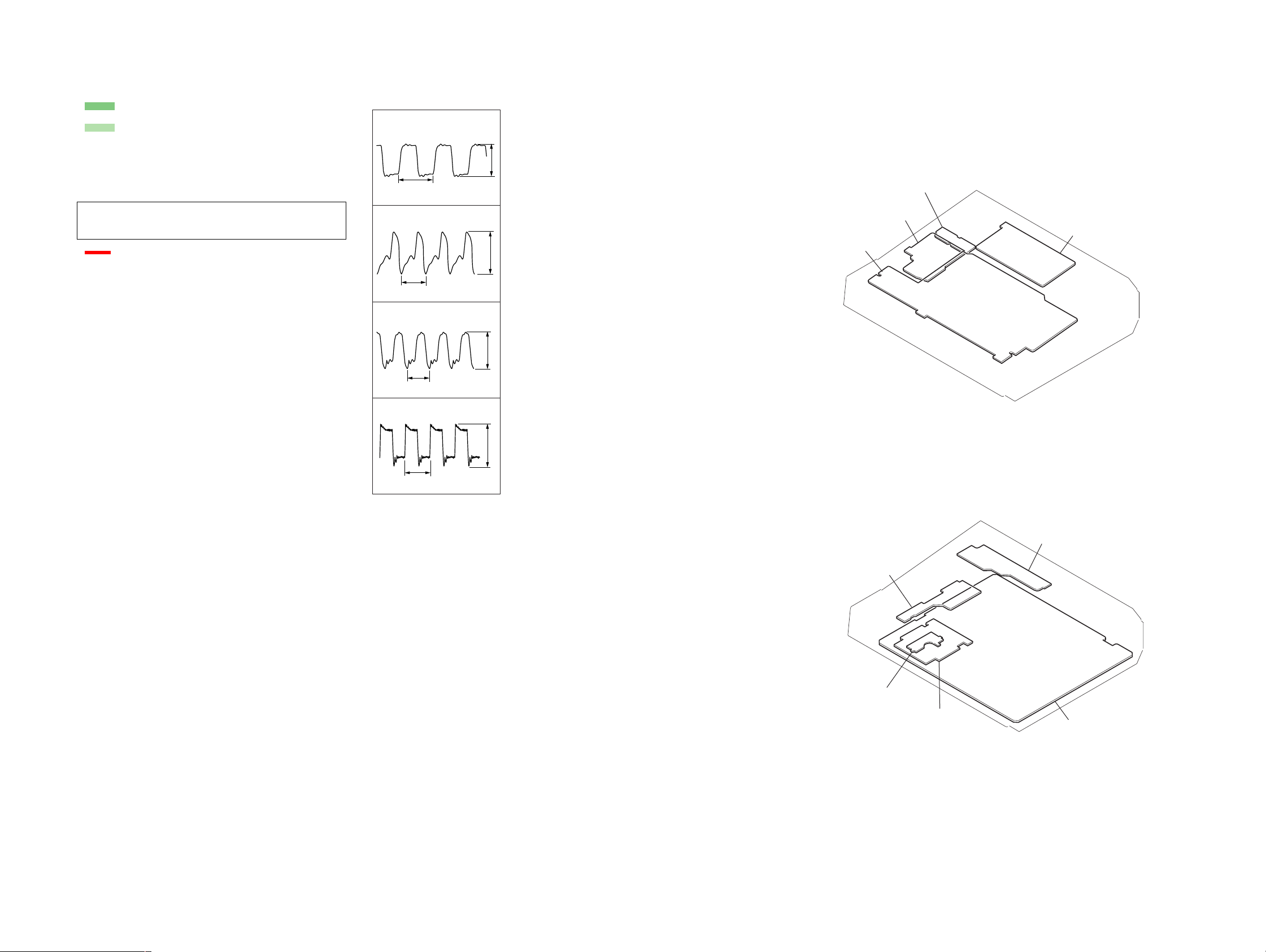
6. EXPLODED VIEWS
6-1. Cabinet Section ·························································· 76
6-2. Key Section ································································ 77
6-3. LCD Section······························································· 78
6-4. MD Mechanism Section (CCMD-2000)···················· 79
7. ELECTRICAL PARTS LIST ······································· 80
NOTES ON HANDLING THE OPTICAL PICK-UP
BLOCK OR BASE UNIT
The laser diode in the optical pick-up block may suffer electrostatic
break-down because of the potential difference generated by the
charged electrostatic load, etc. on clothing and the human body.
During repair, pay attention to electrostatic break-down and also
use the procedure in the printed matter which is included in the
repair parts.
The flexible board is easily damaged and should be handled with
care.
NOTES ON LASER DIODE EMISSION CHECK
Never look into the laser diode emission from right above when
checking it for adjustment. It is feared that you will lose your sight.
CAUTION
Use of controls or adjustments or performance of
procedures other than those specified herein may result in
hazardous radiation exposure.
2
Flexible Circuit Board Repairing
• Keep the temperature of the soldering iron around 270°C during
repairing.
• Do not touch the soldering iron on the same conductor of the
circuit board (within 3 times).
• Be careful not to apply force on the conductor when soldering or
unsoldering.
Notes on chip component replacement
• Nev er reuse a disconnected chip component.
• Notice that the minus side of a tantalum capacitor may be damaged by heat.
SAFETY-RELATED COMPONENT WARNING!!
COMPONENTS IDENTIFIED BY MARK ! OR DOTTED LINE WITH
MARK !ON THE SCHEMATIC DIAGRAMS AND IN THE PARTS
LIST ARE CRITICAL TO SAFE OPERATION.
REPLACE THESE COMPONENTS WITH SONY PARTS WHOSE
PART NUMBERS APPEAR AS SHOWN IN THIS MANUAL OR IN
SUPPLEMENTS PUBLISHED BY SONY.
Page 3

Unleaded solder
Boards requiring use of unleaded solder are printed with the leadfree mark (LF) indicating the solder contains no lead.
(Caution: Some printed circuit boards may not come printed with
the lead free mark due to their particular size.)
: LEAD FREE MARK
Unleaded solder has the following characteristics.
• Unleaded solder melts at a temperature about 40°C higher than
ordinary solder.
Ordinary soldering irons can be used but the iron tip has to be
applied to the solder joint for a slightly longer time.
Soldering irons using a temperature regulator should be set to
about 350°C.
Caution: The printed pattern (copper foil) may peel away if the
heated tip is applied for too long, so be careful!
• Strong viscosity
Unleaded solder is more viscous (sticky, less prone to flo w) than
ordinary solder so use caution not to let solder bridges occur such
as on IC pins, etc.
• Usable with ordinary solder
It is best to use only unleaded solder but unleaded solder may
also be added to ordinary solder.
MDCT-1000
3
Page 4
MDCT-1000
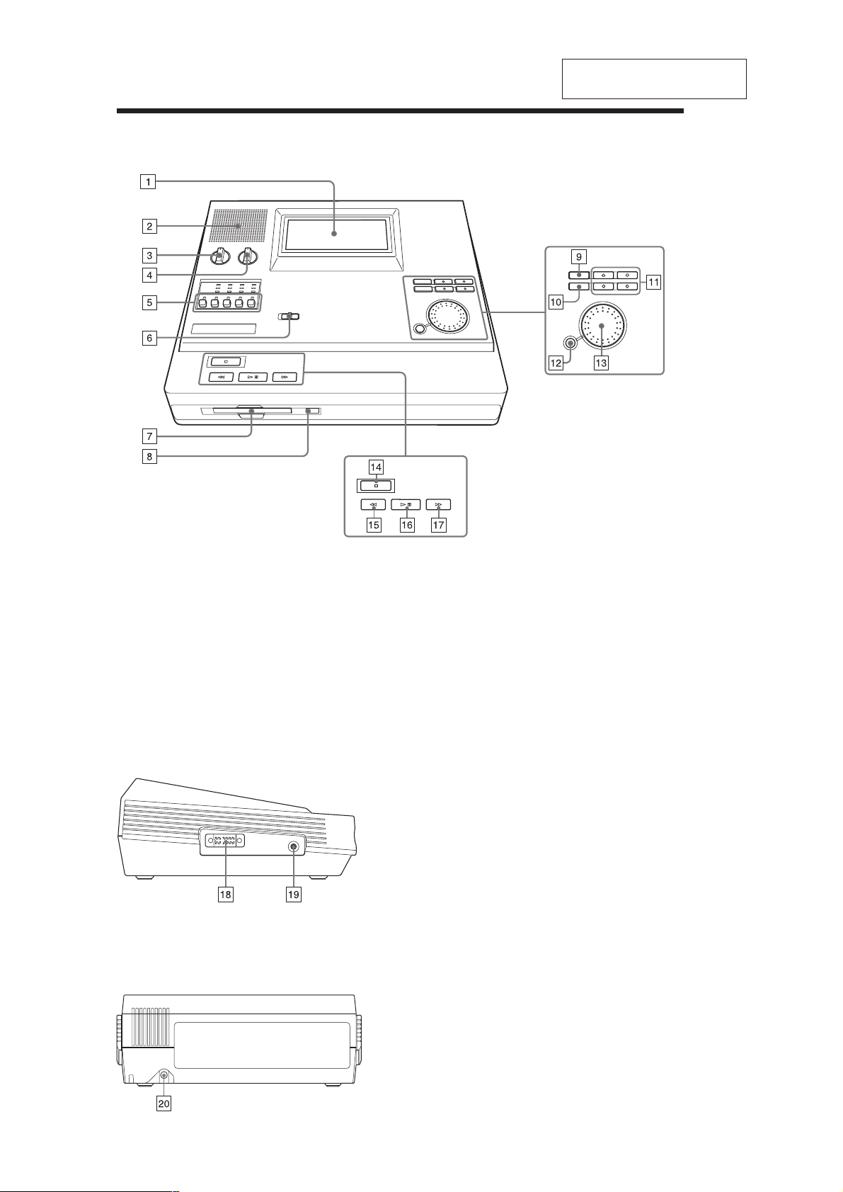
Location and Function of Controls
For details, refer to the pages indicated in ( ).
SECTION 1
GENERAL
This section is extracted from
instruction manual.
1 LCD display
23Built-in speaker
MONITOR VOL control
4 LCD CONTRAST control
Adjusts the contrast of the display.
5 MONITOR select buttons (ALL/1/2/3/4) (8)
6 STANDBY switch
7 MD insertion slot
8 Z EJECT button
Left side
Rear
9 FUNCTION button
q; DISP MODE button (10)
qa Arrow buttons
qs ENTER button
qd Jog dial
qf x STOP button
qg m REW/BS button
qh u PLAY/PAUSE button
qj M FF/FS button
qk CONTROL UNIT connector (11)
ql EAR jack (8)
w; DC IN 12V jack (7)
4
Page 5
Display Window (Information screen)
1
2
3
4
5
6
7
8
MDCT-1000
1 Status display (17)
Indicates the disc inserted in or the status of
deck as follows:
BLANK: a blank disc
NO DISC: no disc
PB ONLY: a commercially available recorded
disc (for playback only)
PROTECTED: a protected disc
RECORDED: a recorded disc
23TIME display
Indicates the recorded time at the current
location for each index item.
(copied) display
Indicates that a disc digitally copied on MDCC2000 is inserted.
4 INDEX counter
Lights up when a disc is inserted.
Blinks during an index search. (9)
5 END display
This shows the end of the disc.
6 Disc status display
Indicates the status of the disc with pictures.
7 Message display
Indicates various data by characters and various
error messages. (17)
8 Disc position display
Indicates the current playback location on the
disc by a white box. Already recorded parts are
indicated in black. The further it is to the right,
the closer the disc is to the end. Depending on the
condition of the disc, the black part might not
reach the far right even if the disc is full.
5
Page 6
MDCT-1000
)
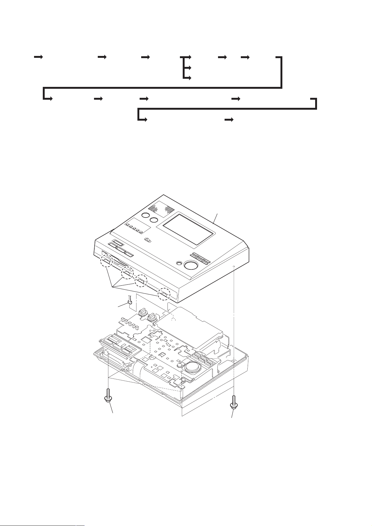
SECTION 2
DISASSEMBLY
• The equipment can be removed using the following procedure. • Disassemble the unit in the order as shown below.
Set
Cabinet (upper) section
Switch section
LCD section
MD section
Main board
Volume section
Door
MD board
Base unit section
BUM-F1 board
REC/PB head assy (HR901) section
Holder assy, cartridge installation Optical pick-up (KMS-250A) section
Note : Follow the disassembly procedure in the numerical order given.
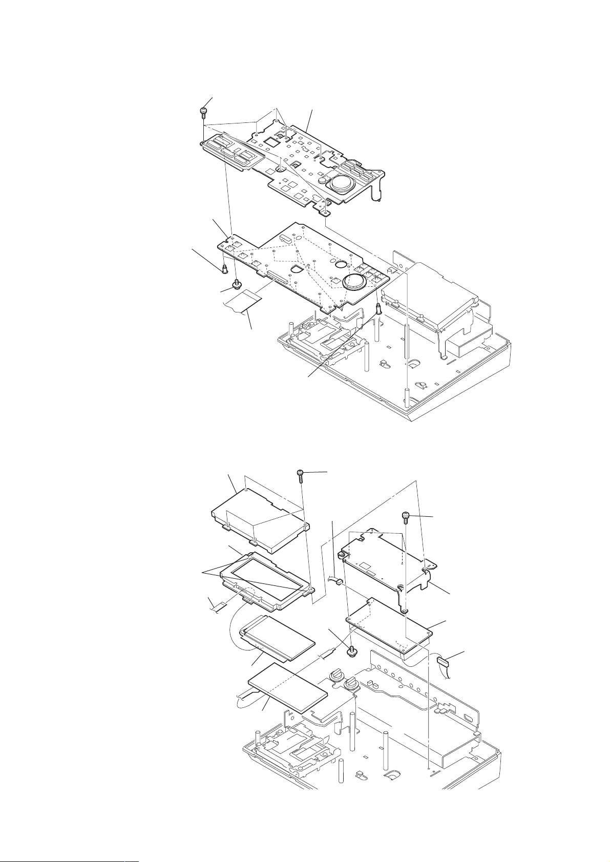
2-1. CABINET(UPPER) SECTION
Holder assy, cartridge section
Cabinet (upper) assy
3
Four claws
4
Connector
(CN9102)
2
Three s
crews (+PSW4
× 1
6)
1
Two s
crews (+PSW4
× 1
6
6
Page 7
2-2. SWITCH SECTION
7
SWITCH board
5
Seven s
(STEP M2)
6
(+PSW 3
crews
Five screws
×
2
Seven
(+PS 3
6)
screws
×
6)
3
Key switch block assy
MDCT-1000
2-3. LCD SECTION
3
Cable, flexible flat
(70mm)
1
Cable, flexible flat (90mm)
Plate (LCD), transparent
2
5
Holder (LCD)
4
Claws
4
Eight s
(STEP M2)
crews
0
Four
(+PSW 3
1
Four
qd
Connector
(CN4002)
screws
×
6)
screws (+PS 2
×
8)
9
(+PS 3
Three
screws
×
qa
LCD bracket
qf
LCD board
6)
6
LCD
8
Light unit, back
7
qs
Connector
(CN4001)
7
Page 8
MDCT-1000
2-4. MD SECTION
3
Three screws
(+PS 3
4
MD mechanism
×
6)
5
Connector(CN9101)
1
Cable, flexible flat
(295mm)
2
Screw
(+PS 3
×
6
Two screws
(+PSW 3
7
6)
× 8
)
AUDIO I/O board
2-5. V OLUME SECTION
qg
Screws
(+PSW 3
qd
(CN9001)
qh
×
Connector
FOOT SWITCH board
9
Two screws (+PS 3
4
2
(CN9202)
Two screws
qf
8)
(+PSW 3
5
Knob(VOL)
6
Two nuts
7
Spacer
×
Level meter bracket
Connector
×
6)
qs
(CN8001)
6)
Connector
3
Three screws (+PS 3
1
Connector(CN6002)
qa
LEVEL METER board
0
Screw
(+PSW 3
×
×
8
VOLUME board
6)
6)
8
Page 9
2-6. MAIN BOARD
6
5
Four screws
(+PSW 3
MAIN board
×
6)
MDCT-1000
3
Connector(CN111)
4
Cable, flexible flat
(295mm)
1
2
Cabinet (lower)
9
Page 10
MDCT-1000
2-7. DOOR
2-8. MD BOARD
spring, door return
1
Release the hook.
5
Tw o
screws
(M 2
×
3)
3
Door
2
Release the boss.
6
MD board
4
Tw o
screws
(M 2
×
3)
10
1
Flexible wire
(18 core, CN5)
2
Flexible board
(CN3)
3
Flexible board
(CN1)
Page 11
2-9. BASE UNIT SECTION
3
Two screws (step)
5
Base unit
4
Two screws (step)
1
S
crew
(toothed lock M 2
MDCT-1000
×
3.5)
2-10. BUM-F1 BOARD
4
Two s
(precision +M 1.7
crews
5
Claw
×
2.2)
7
BUM-F1 board
2
6
Lug, 2
Claw
3
Flexible board
(CN302)
2
Flexible board
(CN304)
1
Plam flexible board
(CN303)
11
Page 12
MDCT-1000
2-11. REC/PB HEAD ASSY (HR901) SECTION
2
Lug, 2
1
S
crew
(toothed lock M 2
×
3.5)
5
G
uide, screw
4
S
crew
(toothed lock M 1.4)
6
Tw o
screws
(M 1.7
×
2.8)
3
Motor, DC geared
(M903)
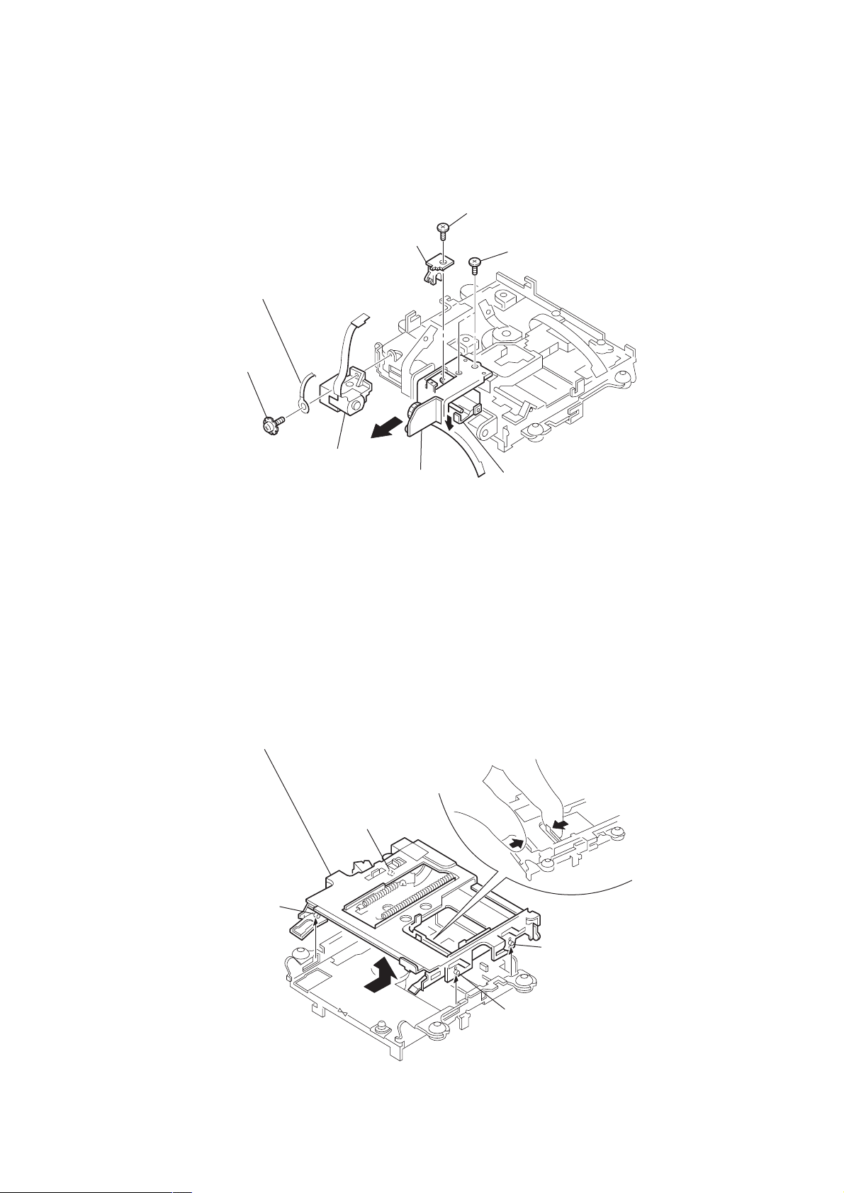
2-12. HOLDER ASSY, CARTRIDGE SECTION
2
While releasing the four bosses, remove
the cartridge holder assembly in the
direction of the arrow
C
.
8
REC/PB head assy
(HR901)
1
the arrows
Boss
7
Removed hook
Push it in the direction of
A
and B with fingers.
A
B
12
Boss
Boss
C
Boss
Page 13
2-13. HOLDER ASSY, CARTRIDGE INSTALLATION
When installing the cartridge holder, coat
the portion
grease (EM-30L).
A
shown in the illustration with
A
Position
A
Position
MDCT-1000
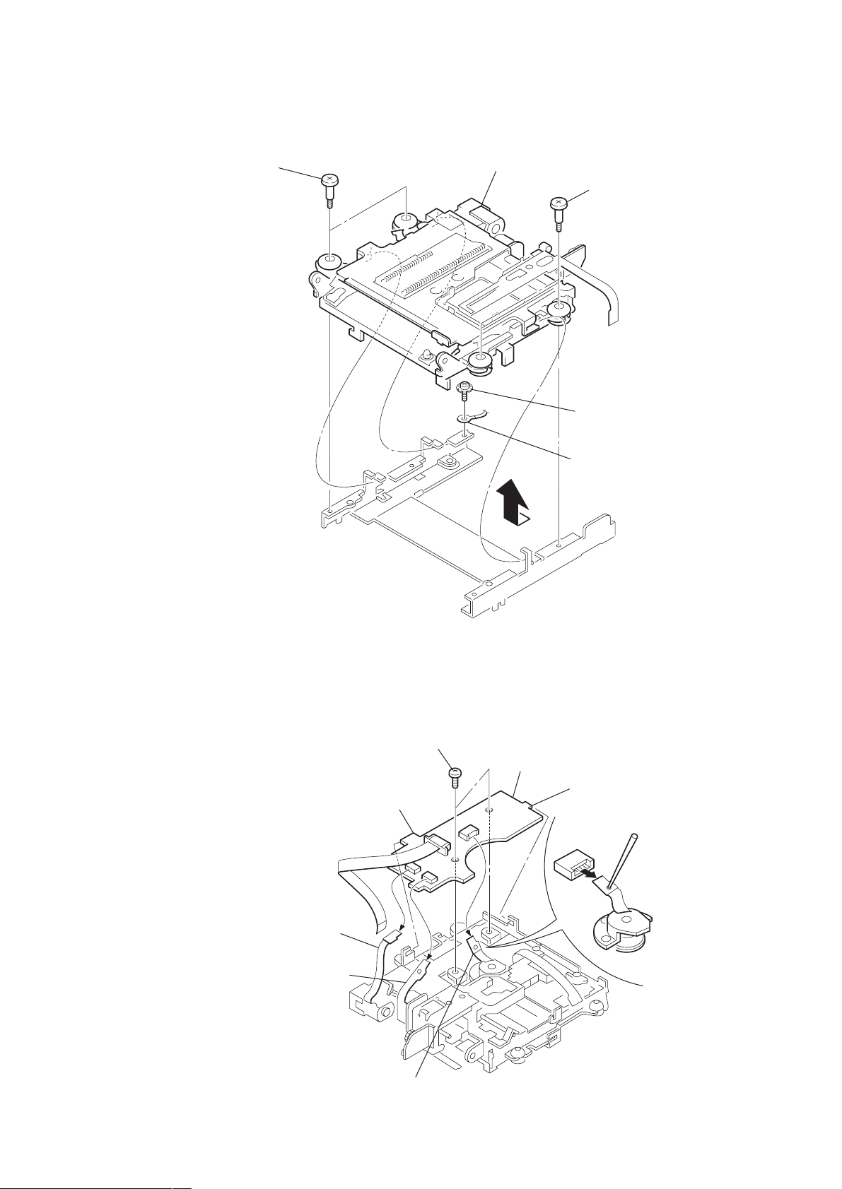
2-14. OPTICAL PICK-UP (KMS-250A) SECTION
4
Spring, g
uide shaft retainer
3
Two screws
(Precision, +P 1.7
×
2.2)
A
5
Two screws
(M 1.7
Position
×
4.5)
6
Two washers
2
Motor, stepping
(M902)
1
Two screws
(Precision, +P 1.7
×
2.2)
7
Optical pick-up (KMS-250A)
13
Page 14
MDCT-1000
SECTION 3
TEST MODE
NOTE
This machine does not have either DECK B nor the
recording function.
3-1. Description
3-1-1. How to Enter the Test Mode
Pressing the G G ENTER g g g g g ENTER G G
ENTER F buttons.
3-1-2. How to Exit the Test Mode
While pressing the G button, rotate the JOG dial and set
“k_test_h” to “0”.
3-1-3. How to Cancel the ENTER key
The numeric keys that have been input up to the moment can be
canceled at the following so that the machine does not enter the
test mode unless otherwise needed.
1. When the interval of pressing the previous numeric key and
the next key exceeds one second or more.
2. When the deck select key is pressed.
3. When the k_mode changes.
4. When the selected deck has changed.
5. When the test mode is set.
3-1-4. How to Select the Test Item
The test item can be selected by “k_test_h” and “k_test_l”.
1. Displaying the selected item
The selected item is displayed on LCD as follows.
Value of “k_test_h” (Displayed in hexadecimal number)
Value of “k_test_l” (Displayed in hexadecimal number)
3-1-5. T est Display
01 - 00 (Top menu)
00 - 00 EXIT (Exit)
01 - 00 THIS MENU (Top menu)
02 - 00 AUDIO (Audio firmware test)
03 - 00 MECH (Mechanism test)
04 - 00 DISPLAY (Display system test)
05 - 00 KEY (Key test)
06 - 00 COMMUNICATION (Communication test)
07 - 00 AUDIO HW (Audio hardware test)
08 - 00 DIGITAL HW (Digital hardware test)
09 - 00 NVRAM (NVRAM test)
3-1-6. Communication with Mechanism Deck
Communication with the mechanism deck is performed using
programs such as “Hyper terminal” or the like that have been
started up on a PC.
Refer to 3-3-3. “Selecting the Terminal”.
(Communication control with the log system or trace monitor is
not possible.)
3-1-7. Circuit Block
General purpose port
KEY
CPU
CPU bus
1809
NVRAM
ROM
CLOCK
SRAM
FIFO8655
DRAM
LCD
05 - 01
/* KEY INCREMENT TEST */
2. How to select the test item using the JOG dial
1. While pressing G b utton, rotate the JOG dial. “k_test_h”
changes.
When “k_test_h” changes, “k_test_l” is set to “0”.
Select the desired test category using “k_test_h”.
2. While pressing g button, rotate the JOG dial. “k_test_l”
changes.
Select the desired test item using “k_test_l”.
3. Sets the selected test item either by pressing g button
after selecting “k_test_l” or by pressing the ENTER
button.
3. How to select the test item with the use of the PC remote
command
The desired test item can be selected by sending the remote
command of rewriting “k_test_h” and “k_test_l” from the PC
to the machine.
When the “k_test_h/l” change command is sent from a PC to
the machine while the “k_test_h/l” change inhit bit is being
set, the machine returns NAK and the machine does not chanage
“k_test_h/l”.
DECK A
CODEC
AD/DA
3-2. Audio Firmware Test: [AUDIO]
SF data storage method in the DRAM.
• Test program is stored as shown below.
(Operations start in the order starting from channel 1, channel 2,
channel 3, and up to channel 4 under the ordinary operation
conditions but the test mode starts from channel 1, channel 3,
channel 2, and channel 4 in this order.)
0123
1chSF
3ch 2ch 4ch
FIF012 CXD1858 1.2ch
FIF034 CXD1858 3.4ch
LCD: Types, conditions and others of the test are displayed on
the LCD during each test.
Channel selector and channel selector LED: Select the channel
selector by manual operation.
Voice mirror: Change the input level by manual operation.
14
• Perform the following tests after the machine is set in the “STOP”
mode.
02-00 /* AUDIO-F TEST MENU */
02-00 AUDIO-F MENU
Page 15

MDCT-1000
3-2-1. Audio Recording and Playback Test without Disc
• The audio signal (up to the full memory capacity of the DRAM
at a maximum) is recorded in the ATRAC data recording area in
the DRAM and is played back.
• Note: If the audio sources of channel 1 to channel 4 are all the
same,
• Playback is slower than normal if the 4 channels are recorded
and 2 channels are played back.
(The pitch of the playback remains unchanged and the
playback speed of it is half of normal.)
• Playback is faster than normal if the 2 channels are recorded
and 4 channels are played back.
(The pitch of the playback remains unchanged and the speed
of it is double of normal.)
02-01 4ch-REC on DRAM
02-02 4ch-PLAY on DRAM
02-03 2ch-REC on DRAM
02-04 2ch-PLAY on DRAM
02-05 reserve
02-06 reserve
3-2-2. Microphone Sound Monitoring from Speaker during Stop
• Application: For testing “ripping” sound of speak er (Sweep sound
is input from external source.)
• Application: For testing the voice mirror LED (sound is input
from external source.)
02-07 REC_MONI, SP, 1-4ch
3-2-5. Audio Muting T est
• ROM_PB (990Hz, -0.2dB, 1 to 4ch)
02-19 XMUTE=on, MODE=00, (During ROM_PB, circuit playback + mute)
02-1A XMUTE=on, MODE=01, (During ROM_PB, circuit recording + mute)
02-1B XMUTE=on, MODE=10, (During ROM_PB, circuit STOP + mute)
02-1C XMUTE=on, MODE=11, (During ROM_PB, circuit STANDBY + mute)
02-1D XMUTE=off, MODE=00, (During ROM_PB, circuit is in playback.)
02-1E XMUTE=off, MODE=01, (During ROM_PB, circuit is in record.)
02-1F XMUTE=off, MODE=10, (During ROM_PB, circuit is STOP.)
02-20 XMUTE=off, MODE=11, (During ROM_PB, circuit is STANDBY.)
3-3. Mechanism Deck: [MECH]
03-00 /* MD TEST MENU */
01-0E .....etc
10-1F DECK-A Only (Check & Setting)
20-2F DECK-B Only (Check & Setting)
30-3F DECK-A Only (Display Log)
40-4F DECK-B Only (Display Log)
50-57 Laser Check
3-3-1. Displaying the Number of Times of Using the Lasers
The number of times of using the lasers of the deck-A and deckB is displayed.
The number of times of using the lasers is stored in the NVRAM,
and the number of times that the laser power has entered the MO
write (number of clusters), is displayed.
3-2-3. ROM Playback 1
• The pseudo ATRAC data on the EPROM is copied to the 1SG
area on the DRAM and is played back repeatedly.
• Application: Level/Frequency response test
02-08 990Hz, -0.2db, 1-4ch (For playback of the reference level)
02-09 43Hz, -0.2db, 1-4ch
02-0A 10KHz, -0.2db, 1-4ch
02-0B 990Hz, -12db, 1-4ch
02-0C Infinity, 0, 1-4ch (For S/N test)
3-2-4. ROM Playback 2
• The pseudo ATRAC data on the EPROM is copied to the 1SG
area on the DRAM and is played back repeatedly.
• Application: Separation/Frequency response test
• Other channels : No sound
02-0D 990Hz, -0.2db, 1ch
02-0E 990Hz, -0.2db, 2ch
02-0F 990Hz, -0.2db, 3ch
02-10 990Hz, -0.2db, 4ch
02-11 43Hz, -0.2db, 1ch
02-12 43Hz, -0.2db, 2ch
02-13 43Hz, -0.2db, 3ch
02-14 43Hz, -0.2db, 4ch
02-15 10KHz, -0.2db, 1ch
02-16 10Hz, -0.2db, 2ch
02-17 10Hz, -0.2db, 3ch
02-18 10Hz, -0.2db, 4ch
03-01
DECK-A Laser Cnt = xxxxxxxx
DECK-B Laser Cnt = xxxxxxxx
3-3-2. Displaying Temperature of Mechanism
The temperatures of the mechanism of deck-A and deck-B are
displayed.
The temperature of mechanism indicates the temperature inside
the RF amplifier mounted on this machine. However, use this
temperature as a reference value because it is not highly accurate.
03-02
Thermo
DECK-A 35˚C
[Result] = [55] [0B] [58] [62] [07] [09] [09]
DECK-B 31˚C
[Result] = [55] [0B] [58] [5F] [06] [06] [06]
3rd byte of the above [Result] data string : Initial value of the
temperature sensor at 25˚C
4th byte of the above [Result] data string : Present temperature
sensor value
3-3-3. Selecting the Terminal
Select the PC terminals (RS-232C) on the rear of this machine.
Either one of the two patterns “Other” and “Mech”, can be
selected.
Other : For checking contents, etc of the system memory
Mech : For checking status of the mechanism operation
03-0A
Terminal Mode = Mech
15
Page 16
MDCT-1000
The PC should use the terminal software (such as Hyper-T erminal
or Tera-Term).
Sets the communication as follows.
Baud rate : 9600 bps
Data length : 8 bits
Parity : None
Stop bit : 1
Flow control : None
3-3-4. Dump List
Displays the Dump-List of the specified address.
Sets the address value (Adrr) and number (Num) of display bytes
by rotating the JOG dial and pressing ENTER button.
03-0D
Adrr = 00000000 Num = 00
3-3-5. Deleting (Deck-A/Deck-B)
Performs deletion of the disc data.
03-14 (DECK-A)
03-24 (DECK-B)
3-3-6. OA (Inner track, Middle track and Outer track) (Deck-A/
Deck-B)
Performs the OA (overall) test against the inner track (UTOC
area)/Middle track/Outermost track.
Performs “Write”, “Read”, and “Verify” for every 1 cluster as
many as 10 clusters in each area.
03-15 (DECK-A)
03-25 (DECK-B)
Result display
When the OA test of each area has ended with success, the
following message appears on the LCD.
When the “Mech” position of the terminal is selected, the test
status can be checked as follows.
Description of the contents displaying the test status
Example of display
$$ TEST-drv [CNT] (W/R/D/S) (TW/TR) (Result)
drv : Drive No.
CNT : Number of times of test
W : Number of times of “Write” error
Number of times of the write failure for the single
write command (“Seek” error is not included.)
R : Number of times of “Read” error
Number of times of the read failure for the single
read command (“Seek” error is not included.)
D : Number of times of alternation
Number of times of giving-up to write into the
specified cluster
S : Number of times of “Seek” error
Number of times that “Seek” error has occurred
TW : Number of times of TOC “Write” error
Number of times of the TOC write failure for the
single TOC “Write” command (“Seek” error is no
included.)
TR : Number of times of TOC “Read” error
Number of times of the TOC read failure for the
single TOC “Read” command (“Seek” error is no
included.)
Result : Test result up to present (1 : OK, 0 : NG)
Result display
When the OA test has ended with success, the following
message appears on the LCD.
***
Total OK
***
3-3-8. Checking Operations of Mechanism (Deck-A/Deck-B)
Operations of the mechanism are checked using the terminal.
***
Total OK
***
• After the above message appears with normal end, the disc is
ejected automatically.
3-3-7. OA (Overall Test for Normal Recording ) (Deck-A/Deck-B)
The OA test in the same operation as the normal recording is
performed.
The process of “Write”, “Read” and “Verify” is performed for
every 1 cluster starting from the innermost track of the recording
area to the outermost track. Then the “UTOC Write” is performed
for every 10 clusters.
03-16 (DECK-A)
03-26 (DECK-B)
03-17 (DECK-A)
03-27 (DECK-B)
y
Dedicated for
mechanism
Waiting for ’ . ’
y
>>
Mechanism test Prompt
:MON>
Waiting for mdmon
n
Waiting for exit Waiting for command
ny
Operation step
Step 1 : Enters the test mode of the mechanism.
Step 2 : Type in “mdmon” against “MON>” and set it.
Step 3 : Press the ENTER button several times until the
machine enters the test mode dedicated for
mechanism.
Step 4 : Performs the operation check in accordance with
the display output.
Step 5 : Type in “.” to return to “Prompt”.
Step 6 : Type in “exit” to set the operation and exit the
test mode of the mechanism.
n
16
Page 17

MDCT-1000
3-3-9. Eject (Deck-A/Deck-B)
Ejects the disc.
03-18 (DECK-A)
03-28 (DECK-B)
3-3-10. Clearing the Number of Times of Using the Laser
(Deck-A/Deck-B)
The number of times of using the laser is stored, and is cleared as
follows.
It is necessary to clear the number of times data of using the laser
whenever the laser is replaced.
03-19 (DECK-A)
03-29 (DECK-B)
DECK-B Laser Count Clear
NV-RAM Save OK
3-3-11. OA (Overall Test for Random Recording )
(Deck-A/Deck-B)
The (OA) overall test is performed using the same operation as
that of the normal recording.
The “write”, “read”, and “verify” are performed at every cluster
at random within the recording area. The “UTOC write” is
performed at every ten clusters.
The test ends after the specified time has passed.
When the “Mech” position of the terminal is selected, the test
status can be checked as follows.
Description of the contents displaying the test status
Example of display
$$ TEST-drv [CNT] (W/R/D/S) (TW/TR) (Result)
drv : Drive No.
CNT : Number of times of test
W : Number of times of “Write” error
Number of times of the write failure for the single
write command (“Seek” error is not included.)
R : Number of times of “Read” error
Number of times of the read failure for the single
read command (“Seek” error is not included.)
D : Number of times of alternation
Number of times of giving-up to write into the
specified cluster
S : Number of times of “Seek” error
Number of times that “Seek” error has occurred
TW : Number of times of TOC “Write” error
Number of times of the TOC write failure for the
single TOC “Write” command (“Seek” error is no
included.)
TR : Number of times of TOC “Read” error
Number of times of the TOC read failure for the
single TOC “Read” command (“Seek” error is no
included.)
Result : Test result up to present (1 : OK, 0 : NG)
3-3-12. Rescue (2-channel Mode) (Deck-A/Deck-B)
When the UTOC information shows error, the disc can be
recovered as follows.
03-1E (DECK-A)
03-2E (DECK-B)
DECK-A Rescue 2Ch Mode
Disc-Input!!
Result display
Index structure : Only 1 index is used over the entire area
of a disc.
Recording mode : 2-channel mode
Original : Original
Name information : Invalid
Time information : Invalid
3-3-13. Rescue (4-channel Mode) (Deck-A/Deck-B)
When the UTOC information shows error, the disc can be
recovered as follows.
03-1F (DECK-A)
03-2F (DECK-B)
DECK-A Rescue 4Ch Mode
Disc-Input!!
Contents of recovery
Index structure : Only 1 index is used over the entire area
of a disc.
Recording mode : 4-channel mode
Original : Original
Name information : Invalid
Time information : Invalid
3-3-14. Laser Power OFF (Deck-A/Deck-B)
Turns off the laser power.
03-50 (DECK-A)
Laser Power (DECK-A) = OFF
[Result] = [01] [1D] [00] [00] [00] [00] [00]
03-54 (DECK-B)
Laser Power (DECK-B) = OFF
[Result] = [01] [1D] [00] [00] [00] [00] [00]
3-3-15. Laser Power MO-WRITE (Deck-A/Deck-B)
Sets the laser power to the “MO-WRITE”.
03-51 (DECK-A)
Laser Power (DECK-A) = MO-WRITE
[Result] = [01] [1D] [00] [18] [00] [01] [00]
03-55 (DECK-B)
Laser Power (DECK-B) = MO-WRITE
[Result] = [01] [1D] [00] [18] [00] [01] [00]
Result display
When the OA test has ended with success, the following
message appears on the LCD.
***
Total OK
***
3-3-16. Laser Power CD-READ (Deck-A/Deck-B)
Sets the laser power to the “CD-READ”.
03-52 (DECK-A)
Laser Power (DECK-A) = CD READ
[Result] = [01] [1D] [00] [08] [00] [02] [00]
03-56 (DECK-B)
Laser Power (DECK-B) = CD READ
[Result] = [01] [1D] [00] [08] [00] [02] [00]
17
Page 18
MDCT-1000
3-3-17. Laser Power MO-READ (Deck-A/Deck-B)
Sets the laser power to the “MO-READ”.
03-53 (DECK-A)
Laser Power (DECK-A) = MO READ
[Result] = [01] [1D] [00] [08] [00] [03] [00]
03-57 (DECK-B)
Laser Power (DECK-B) = MO READ
[Result] = [01] [1D] [00] [08] [00] [03] [00]
3-4. Display System Test: [DISPLAY]
04-00 /* DISPLAY TEST MENU */
04-01 [LCD_cntr] - [u_com] : connection check
[LCD_cntr] - [h_sram] : connection check
[LCD_cntr] - [LCD] : connection check
04-02 LCD DOT all set
04-03 LCD DOT all clear
04-04 character check on h_sram (SAG1) [1]
04-05 character check on h_sram (SAG1) [2]
04-06 [u_com - [LCD_cntr] : test signal
04-07 transmission of character data
04-08... content of global_area_address
• Connecting the Microprocessor with LCD Controller
Microprocessor
AO
XRD
XHWR
XCS4
16MHz
D15
D14
D13
D12
D11
D10
D9
D8
XRES
Divide-by-2
Reset IC
LCD controller
AO
XRD
XWR
XCS
8MHz
XRES
• Connecting the LCD Controller with SRAM
LCD controller
VA15
VA14
VA13
VA12
VWR
VRD
VA14
VA13
VA12
VA11
VA10
VA9
VA8
VA7
VA6
VA5
VA4
VA3
VA2
VA1
VA0
D7
D6
D5
D4
D3
D2
D1
D0
ADDRESS
0000 to 6FFF
7000 to EFFF
F000 to FFFF
123
H
L
L
H
H
H
L
H
L
AND
AND OR
1
Buff
2
[SRAM]
• 1st layer (Character screen)
0 (0000h) to 9999 (270Fh)
• 2nd layer (Graphic screen)
10000 (2710h) to 19999 (4E1Fh)
• SAG1 (Character storage)
61440 (F000h) to (FFFFh)
3
AND
VCE
18
Page 19
MDCT-1000
• Connecting the LCD Controller with LCD
LCD controller LCD
WF
LP
XSCL
YDIS
YD
D0
D1
D2
D3
XRES
Reset IC
PA4 (Microprocessor)
LP
DELAY
AND
OR
DF
LOAD
CP
FRAME
DISP
3-4-1. Connection Check between Microprocessor and LCD
Controller, and between LCD Controller and SRAM
• Check the checksum of the font and the graphic data that are
transferred to SAG1 (F000h to FFFFh) of the SRAM for display
when releasing the STANDBY mode.
[Calculation is under way.]
04-01
(data read from LCD cntr) = ????????
• When [OK] appears:
Connection between the microprocessor and LCD controller and
the connection between LCD controller and SRAM are correct.
04-01
(data read from LCD cntr) = xxxxxxxx
3-4-2. LCD Dot Check (Lighting All Dots)
Lighting all dots of LCD (Graphic data: By 0xff transfer)
04-02
3-4-3. Checking the LCD Dot (Turning off all dots)
All dots of LCD are turned off. (Graphic data : By 0x00 transfer)
04-03
3-4-4. Test Signal Output from Microprocessor to LCD Controller
Test signal output is under preparation.
04-06
NOW test signal loading...
Test signal is under preparation.
0xff and 0x00 are output repeatedly to the microprocessor ports
D15 to D8 as follows.
About 0.25 S 0.25 0.25 0.25
About 30 seconds
The test signal output ends.
04-06
finished test signal output
3-5. Key Test: [KEY]
05-00
/* KEY TEST MANU */
05-01 KEY INCREMENT TEST
05-02 ANY KEY TEST
05-03 K_mode LOG
[OK]
• When [NG] appears:
1. If the following *NG display is recognized, “XRD” is
suspected.
2. If the following *NG display is not recognized (upon
confirmation through trace monitor), either one of the
connections between microprocessor and LCD controller or
the connection between LCD controller and SRAM or the
connection between LCD controller and LCD is defective.
(At this time, if the test signal is output from the microprocessor
to LCD controller in step 04-06, whether the connection is OK
or NG can be confirmed, and also which of the connections
between LCD controller and SRAM or the connection between
LCD controller and LCD is NG.)
04-01
(data read from LCD cntr) = KKKKKKKK
[NG]
Mabye read pattern NG. or.
[LCD_cntr]-[u_com],[h_sram]: connect NG
3-5-1. Key Test by Pressing Keys in Order
05-01
/* KEY INCREMENT TEST */
Turn ON
⇒ DISPLAY(A)
When the specified “DISPLAY (A)” key is pressed correctly, the
following messages appear.
05-10
/* KEY INCREMENT TEST */
⇒ DISPLAY(A)
OK
Turn OFF
19
Page 20
MDCT-1000
When releasing your finger from the key , the next ke y to be pressed
is specified.
When an incorrect key that is different from the specified one is
pressed, following messages appear.
05-10
/* KEY INCREMENT TEST */
⇒ DISPLAY(A)
NG
Turn OFF
The test cannot be advanced unless the correct key is pressed.
The “Key Test by Pressing Keys in Order” is complete.
(Normally end)
When all of the key pressings are correct,
“COMPLETE”
appears on the LCD screen and type in 05-42.
(Abnormally end)
When the incorrect key is pressed more than once,
“xxxxx
at FAULT”
appears on the LCD screen.
An incorrect key that was detected at first in the order of pressing keys,
is displayed in “xxxxx”.
3-5-2. Key Test by Pressing Arbitrary Key
05-02
/* KEY TEST */
PUSH KEY : OFF (FF/F5-FF)
AD CODE : FF FF FF FF FF FF FF
TRANSCRIBE : A POW : ON
SEARCH MODE : INDEX JOG : 00
Displays the name of the pressed key.
Example : When the STOP button of the deck-A is pressed,
05-05
PUSH KEY : STOP (A) (00/00-09)
appears.
The first 2-digit “00” of (00/00-09) indicate the value that the
pressed key after it is conv erted by AD con verter. The digits “00-
09” indicate the range when the key is judged as “STOP (A)”.
Allocation of key groups and keys
Application
Type
Group
Allocation of Kn
Application
Type
Group
Allocation of Kn
Application
Type
Group
Allocation of Kn
Foot switch
operation
0
FS_PLAY
1
FS_FS
2
FS_BS
3
4
5
6
7
8
9
10
Operation of the
mechanism
0
STOP(A)
1
STOP(B)
2
PLAY/PAUSE(A)
3
REW/REV(A)
4
FF/CUE(A)
5
MARK(A)
6
MARK_OFF(A)
7
8
9
10
FUNCTION
0
f
1
F
2
DEL
3
<(LEFT)
4
>(RIGHT)
5
6
7
8
9
10
ANALOG
0
ANALOG
1
Function
ANALOG
5
Operation of the
mechanism
ANALOG
2
REC(A)
REC(B)
PLAY/PAUSE(B)
REW/REV(B)
FF/CUE(B)
MARK(B)
MARK_OFF(B)
Function
ANALOG
6
ENTER
DISP_MODE(A)
DISP_MODE(B)
Operation of the
mechanism
ANALOG
3
INDEX
EJECT(A)
EJECT(B)
DECK_A
DECK_B
SEARCH
Function
ANALOG
7
REC_PAUSE
Search
ANALOG
4
0
1
2
3
4
5
6
7
8
9
10
Power supply,
etc.
DIGITAL
8
Use is prohibited
Use is prohibited
A/B(FS)
INDEX/TIME
STANDBY/ON
AD CODE
Displays values when the key inputs are converted by AD
converter, in the order starting from 0 up to 7 from the left of
the LCD screen.
05-05
Group 0
AD CODE : FF FF FF FF FF FF FF
Group 7
20
Page 21

MDCT-1000
3-6. Communication Test: [COMMUNICATION]
• RS232-C connector
When the pin-2 and pin-3 of the RS232-C connectors are
connected, two values are displayed in the 2-digit hexadecimal
values respectively on the LCD screen, one is the send data and
the other is data that have been received by the loop-back.
Display example
Tx DATA 57 ← Send data.
Rx DATA 57 ← Received data.
The value of the receiv ed data follows a little bit delayed after the
send data.
The send data increments at every about 0.5 seconds.
• Modular jack
When pin-2 and pin-3 of the modular jack are connected to pin3 of the RS232-C connector, the same test can be done.
• Communication packet
The status packet is used.
Packet size = 38 bytes
06-00
/* PC_I/F LOOP BACK */
Tx DATA = xx
Rx DATA = xx
3-7. Audio Hardware Test: [AUDIO HW]
• The following test should be performed while the machine is set
in the “STOP” mode.
07-00 /* AUDIO-H TEST MENU */
07-00 AUDIO-H MENU
07-01 RESERVE
3-7-1. Testing the Alarm Sound
07-02 XMUTE=on, MODE=00 (During alarm, circuit playback + mute)
07-03 XMUTE=on, MODE=01 (During alarm, circuit recording + mute)
07-04 XMUTE=on, MODE=10 (During alarm, circuit STOP + mute)
07-05 XMUTE=on, MODE=11 (During alarm, circuit STANDBY + mute)
07-06 XMUTE=off, MODE=00 (During alarm, circuit is in playback.)
07-07 XMUTE=off, MODE=01 (During alarm, circuit is in record.)
07-08 XMUTE=off, MODE=10 (During alarm, circuit is STOP)
07-09 XMUTE=off, MODE=11 (During alarm, circuit is STANDBY)
3-7-2. T esting LED
07-0A LED=4ch, LED=on
07-0B LED=2ch, LED=off
3-7-3. Stopping FINT Information
07-0C FINT INFORMATION
3-8. Digital Hardware System Test: [DIGITLAL HW]
• Performs the menu display of the digital system test items.
• SRAM test
Write/read test of the SRAM area is performed at the startup when
the main power is turned on.
0x5555, 0xAAAA and 0x0000 are used as the write data.
After completion of the writing the respective data, the data are
read-out and are collated.
The test area is 0x200000 to 0x207FFF in the area 1.
When an error occurs during reading and collating, the REC LED
on the deck-A will blink permanently.
(The REC LED on the deck-A is connected to the pin-11 (PC0)
of the IC1077 HD64003TF16.
• DRAM test
Write/read test of the DRAM area is performed at the startup
when the main power is turned on.
0x5555, 0xAAAA and 0x0000 are used as the write data.
After completion of the writing the respective data, the data are
read-out and are collated.
The test area is 0x600000 to 0x7FFFFF in the area 3. The test is
performed at every 257 bytes.
When an error occurs during reading and collating, the REC LED
on the deck-B will blink permanently.
(The REC LED on the deck-B is connected to the pin-12 (PC1)
of the IC1077 HD64003TF16.)
3-8-1. The Menu Display
08-01
/* DIGITAL HW TEST */
08-01 THIS MENU
08-02 ROM VERSION & DATE
08-03 ROM CHECK SUM
08-04 JOG INPUT
08-05 PULSE 10 mSEC
08-06 CXD-8655 WRITE/READ
08-07 CLOCK IC
08-08 CLOCK IC (power on)
08-09 LED ON/OFF
08-0A NMI
08-0B MODEL
08-0C LOCAL
3-8-2. ROM Version
Displays the release version of the programmed ROM.
08-02
/* ROM VERSION & DATE */
ROM: Ver No.0017 DATE: 2001.02.21
DECK A ROM : V 2.33
DECK B ROM : V 2.33
3-8-3. Check Sum of the ROM
Checksum of the programmed ROM is calculated.
The checksum area is 0x00000 to 0x07FFFF in the area 0.
Displays the address under calculation in hexadecimal number.
08-03
/* ROM CHECK SUM */
CHECK SUM = xxxx
21
Page 22
MDCT-1000
Displays the calculation result in the 2 bytes hexadecimal number .
The result indicates the value which is the same as checksum
calculated by the ROM writer.
08-FF
/* ROM CHECK SUM */
CHECK SUM = 9375
COMPLETED
3-8-4. Entry by JOG Operation
The input data of the JOG operation is sampled by 1 msec. cycle.
When the input data agree twice continuously, the data are
confirmed as the input data. The confirmed input data pass through
the chattering processing. Then the resultant input data is
displayed.
08-04
/* JOG INPUT */
JOG-1 = 1
JOG-2 = 0 or 1
Displays the input status of the pin-2 of the CPU in the JOG-1.
Displays the input status of the pin-3 of the CPU in the JOG-2.
The JOG-1 is the input at pin-2 (PB0) connector of the IC1077
HD64003TF16.
The JOG-2 is the input at pin-3 (PB1) connector of the IC1077
HD64003TF16.
3-8-5. PULSE Output
• Connection between the CXD-1809 and the CPU bus can be
checked by this test.
08-05
/* PULSE 10mSEC */
The pulse for confirming the clock oscillation of the microprocessor is output.
This pulse is output to pin-73 (RA03) terminal TP1058 of the
IC1033 CXD-1809.
The pulse width is 10 msec and the tolerance is less than 1/100.
10 mSEC 10 mSEC
3-8-6. Write/Read Test of CXD-8655
After writing 0x55 in the “Interrupt Timing Register” of the CXD8655 (IC1021), the value in the same register is read out and is
checked whether the data is 0x55 or not.
3-8-7. Watch IC Test I
Displays the inside data of the watch IC and performs the error
correction of the oscillation clock.
08-07
/* CLOCK DATA */
SECOND = 54 CORRECT = 10
MINUTE = 37 CRTL_1 = 20
OCLOCK = 14 CTRL_2 = 00
WEEK = 00
DAY = 02 SET CORRECT (JOG & ENTER)
MONTH = 91 32769.500 - 32769.599 (10)
YEAR = 00
“MONTH = 91” means a status that the 100-yaer bit is on. It
becomes November by masking MSB.
1. Contents of displays
Items Contents of display
SECOND Displays the value of the “second” count register in 2-digit BCD.
MINUTE Displays the value of the “minute” count register in 2-digit BCD.
OCLOCK Displays the value of the “hour” count register in 2-digit BCD using
24-hour display.
WEEK Displays the value of the “week” count register in 2-digit
hexadecimal number.
No. 0 to No. 7 corresponds to Sunday through Saturday
respectively. But, because this machine does not use the day of
No. 7, the data is different from the actual day of the week.
DAY Displays the value of the “date” count register in 2-digit hexadecimal
number.
MONTH Displays the value of the “month” count register in 2-digit
hexadecimal number.
The bit 7 is set to “1” when the “year” count register is capable up
to 100 years.
YEAR Displays the value of the “year” count register in 2-digit BCD.
Displays the value of the “CORRECT” error correction register
in 2-digit hexadecimal number.
CRTL_1 Displays the value of the control register 1 in 2-digit hexadecimal
number.
Bit name Used for Setup value
7 : WALE Alarm control 0 = Alarm is invalid
6 : DALE Alarm control 0 = Alarm is invalid
5 : 12 24 12-hours/24-hours clock 1 = 24-hours clock
4 : CLEN2 32 kHz output 0 = Valid
3 : TEST IC test 0 = Normal operation
mode
2 : CT2 0 = OFF
1 : CT1 0 = OFF
0 : CT0 0 = OFF
Selecting the
periodic interrupt
08-06
/* CXD- 8 6 5 5 WR/RD */
WRITE/READ COMPLETE.
If value is the same, “WRITE/READ COMPLETE” appears.
If value differs, “WRITE/READ ERROR!” appears.
22
Page 23

MDCT-1000
CRTL_2 Displays the value of the control register 2 in 2-digit
hexadecimal number.
Bit name Used for Setup value
7 : VDSL Power supply monitoring 0 = 2.1V
voltage
6 : VDET Result of power supply 0 = More than
monitoring monitoring
voltage
5 : SCRATCH Scribble bit
4 : XSTP Stops sending data 0 = Normal send
status
3 : CLEN1 32 kHz output 0 = Valid
2 : CTFG Fixed cycle interrupt 0 = OFF
output
1 : WAFG Alarm matches. 0 = Does not match.
0 : DAFG Alarm matches. 0 = Does not match.
SET CORRECT Indicates the method to set the correction value.
32768.500 to Indicates the clock oscillation frequency range.
32768.599 ( ) Indicates the correction value in parenthesis ( ).
2. Error Correction
Corrects an error of the clock oscillation frequency of the watch
IC.
1. Pull up the clock output (TP1001) of the watch IC to the
Vcc with a resistor (about 10 kΩ).
2. Measure the clock oscillation frequency.
The frequency counter which has the measurement accuracy
of eight digits or more should be used.
3. Select the range of the oscillation frequency using the JOG
dial.
4. Press the ENTER button.
When the writing data into the watch IC and the storing
data into the NVRAM are complete, “COMPLETE”
appears.
5. When the ENTER button pressed once and then the hand
removed from the ENTER button, the value that are set in
“CORRECT=” is reflected and stored.
(Note)
In order to return the machine to the customer with the status
in which the clock error correction value is being saved,
select “SHIPPING” in the test mode of the NVRAM and
press the ENTER button, or alternately exit the test mode
and enter the STANDBY mode.
In the latter method, be careful that the stamp information,
password, reverse time, etc are not initialized.
(If the NVRAM is initialized or the pattern write test is
performed, the clock error correction value that is sav ed in
the NVRAM, will also be initialized.)
3-8-8. Watch IC Test II (When power is turned on)
The inside data of the watch IC before executing the backup
battery run-out check is displayed at the moment of immediately
after the power-on of the machine.
Accordingly, the data before resetting the watch IC at the event
of backup battery run-out check, etc can be confirmed.
08-08
/* CLOCK IC (Data just before power on) */
SECOND = 54 CORRECT = 10
MINUTE = 37 CRTL_1 = 20
OCLOCK = 14 CTRL_2 = 00
WEEK = 00
DAY = 02 [OSCILLATOR : OK (CONTINUED) ]
MONTH = 91 [SECOND-YEAR DATA : LEGAL ]
YEAR = 00 [BACKUP BATTERY : OK (MORE THAN 2.1V) ]
“MONTH = 91 becomes November by masking MSB in the status
in which the 100-yaer bit is set to on.
1. Contents of displays
The contents are the same as those of Section 3-8-7. “Watch
IC T est I” except for the following.
Items Contents of displays
[OSCILLATOR : OK (CONTINUED) ] When the oscillation stop
is not detected.
[OSCILLATOR : NG (STOPED) ]
[SECOND-YEAR DATA : LEGAL ]
[SECOND-YEAR DATA : ILLEGAL ]
[BACKUP BATTERY : OK (MORE THAN 2.1V) ] When the backup battery
[BACKUP BATTERY : LESS THAN 2.1V ] When the backup battery
When the oscillation stop
is detected.
When the data of second,
minute, hour, date, month,
and year are of the
possible values.
When the data of second,
minute, hour, date, month,
and year are of the
impossible values.
is normal.
has run out.
3-8-9. LED ON/OFF
The LEDs of the channel 3 and channel 4 of the monitor and
those of LINE OUT, the deck-A and deck-B, and the REC button
simultaneously blink.
08-09
/* LED ON/OFF */
1. 3ch/4ch
2. DECK A/B
3. REC A/B
The period of blinking is 0.5 seconds for “on” and 0.5 seconds
for “off”.
0.5 SEC 0.5 SEC
23
Page 24
MDCT-1000
3-8-10. NMI Test
When the NMI starts, “NMI ON” appears.
08-0A
/* NMI */
NMI ON
“NMI OFF” appears about one second later.
08-0A
/* NMI */
NMI OFF
Outputs the pulse to pin-73 (RA03) terminal TP1058 of the
IC1033 CXD-1809.
Pulse width is about 1 sec.
IC1002-8 PIN
IC1007-72 PIN
IC1033-72 PIN
1 SEC
3-9-1. Setup for Shipment of the Machine
The data except the watch correction value and the number of
times of use of the laser are initialized.
09-01
/* NVRAM INITIALIZE / CHECK */
Setting-up is under way.
Setup for shipment of the machine is under way.
09-10
/* NVRAM SHIPPING */
Result
(Normal completion)
Display of completion of setup for shipment of the machine
09-FF
/* NVRAM SHIPPING */
COMPLETE.
CUT OFF POWER!
Shut off the power supply after this.
(After completion of the test mode by setting k_test_h to 0x00,
you may set the [STANDBY] mode.)
LCD display
"NMI OFF" "NMI ON" "NMI OFF"
3-9. NVRAM Test: [NVRAM]
After writing the word data (2 bytes) with 128 words to the evennumbered address from the address 0x00, write 128 words to the
odd- numbered address from the address 0x01.
After reading and checking at every ev en-numbered address from
the address 0x00, read and check at odd-numbered address from
the address 0x01.
09-01
/* NVRAM INIIALIZE / CHECK */
09-01 SHIPPING
09-02 INITIALIZE
09-03 PATTERN CHECK
SELECT and ENTER
While pressing the g button, rotate the [JOG] dial, then the
setup or test starts by pressing the ENTER button after changed
k_test_l.
• Remote selection
By sending the remote command for the setup of k_test_h and
k_test_l, the test can start to perform directly without operating
buttons of g , [JOG], ENTER , etc.
(Abnormal completion)
Display of the abnormal completion of the setup for shipment
of the machine
09-10
/* NVRAM SHIP INITIALIZE */
ERROR.
REPAIR HARDWARE!
Data of the NVRAM are undefined.
Investigation to perform repair, etc is required.
Initialized data of the NVRAM
Marks Items Values Remarks
A disp_cnt_A/B 0x11 A=Lower 4-bit, B=Higher 4-bit
B deck status 0x00 use, mark_a/b
C mark_clust_a 0x00 Cluster address of the mark A
D mark_clust_b 0x00 Cluster address of the mark B
E mark_sect_a 0x00 Sector address of the mark A
F mark_sect_b 0x00 Sector address of the mark B
G pb_stop (A/B) 0x00 Playback stop position address
H laser (A/B) ? Count of use of the laser
I rec_mode 0x01 Record ATARC mode
J rev_time 0x00 Reverse time
K pass_word 0x00 Password
L correct ? Error correction value of the watch
M reserve 1 Reserved
N crc_int ? CRC of the above
O stamp 0x00 Stamp character string
P crc_stamp ? CRC in stamp character string
24
Page 25

MDCT-1000
3-9-2. Initialization of the NVRAM
09-02
/* NVRAM INITIALIZE/CHECK */
During execution of the initialization, “k_test_l” shows the
following values.
Value of k_test_l Status
0x21 During write.
0x22 During read.
0xFF Completion of the check
Display during initialization
09-20
/* NVRAM INITIALIZE */
NOW NVRAM INITIALIZE.
Result
(Normal completion of the initialization)
If nv_error=0, the initialization has normally ended.
09-FF
/* NVRAM INITIALIZE */
COMPLETE.
CUT OFF POWER.
3-9-3. 4-Pattern Check
09-03
/* NVRAM INITIALIZE / CHECK */
During execution of the check, “k_test_l” shows the following
values.
Value of k_test_l Status
0x31 Data write is in progress. Both even number and odd number
are 0x0000.
0x32 Data read and data check are in progress.
0x33 Data write is in progress. Even number is 0x5555 and odd
number is 0xAAAA.
0x34 Data read and data check are in progress.
0x35 Data write is in progress. Even number is 0xAAAA and odd
number is 0x55555.
0x36 Data read and data check are in progress.
0x37 Data write is in progress. Both even number and odd number
are 0xFFFF.
0x38 Data read and data check are in progress.
0xFF Check is complete.
Display during check
09-31
/* NVRAM PATTERN CHECK */
1. NOW 00-00 PATTERN CHECK
All data of the NVRAM are set up to 0xFFFF (the initial value of
the device).
After this, shut off the power supply.
(Note) The correction information of the watch is set up to “No
correction (0)”.
(Abnormal completion of the initialization)
If nv_error=0x10, the initialization has ended with failure.
09-FF
/* NVRAM INITIALIZE */
ERROR.
REPAIR HEARDWARE!
The data of the NVRAM are undefined.
Investigation to perform repair, etc is required.
(Note) The correction information of the watch is set up to “No
correction (0)”.
Result of the check
(In the normal case)
If nv_error=0, the result is normal.
09-FF
/* NVRAM CHECK */
1. 00-00 PATTERN CHECK OK.
2. 55-AA PATTERN CHECK OK.
3. AA-55 PATTERN CHECK OK.
4. FF-FF PATTERN CHECK OK.
CHECK END.
CUT OFF POWER.
All data of the NVRAM are set up to 0xFFFF (the initial value of
the device).
After this, shut off the power supply.
(Note) The correction information of the watch is set up to “No
correction (0)”.
(In the abnormal case)
If nv_error>0, the result is abnormal.
09-FF
/* NVRAM CHECK */
1. 00-00 PATTERN CHECK OK.
2. 55-AA PATTERN CHECK OK.
3. AA-55 PATTERN CHECK ERROR.
4. FF-FF PATTERN CHECK OK.
REPAER THE HEARDWARE!
Example : An error in write and read of the AA-55 pattern
Investigation to perform repair, etc is required.
(Note) The correction information of the watch is set up to “No
correction (0)”.
25
Page 26

MDCT-1000
SECTION 4
ELECTRICAL ADJUSTMENTS
4-1. LASER POWER ADJUSTMENT
1. Enter the test mode of Checking Operations of Mechanism,
and start up the adjustment program. (Refer to section 3-3-13.
Checking Operations of Mechanism.)
:MON>mdmon
MD DRIVE TEST MODE MONITOR Wait..... Hit ’.’ to exit
>>>PDMD-7 TEST MODE V2.14 [Feb. 16 1998]
>>
2. When the return key is pressed, the menu is displayed.
>>>PDMD-7 TEST MODE V2.14
P)Play A)Access N)Info E)Eject R)Rec K)Erase V)Volum !)Reset
X)Cmd L)Laser F)Focus W)Switch S)Spindl J)Jump G)FGSV D)Sled
M)EEPROM U)Adjust C)Spec T)Still Y)Sync 1)Mon 2)Aging
>>
3. Select U)Adjust.
>>u
1)TEMP 2)LASER 3)EFBL/SERVO/FBIAS
5)EFBL 6)SERVO 7)FBIAS E)Eject >>
4. Select 2) LASER.
1)TEMP 2)LASER 3)EFBL/SERVO/FBIAS
5)EFBL 6)SERVO 7)FBIAS E)Eject >>2
--- READJUST?
5. Set the laser power meter (J-2501-046-A) and press the return
key.
>>WRITE POWER : 6.85 mW
1)- 2)+ [DA] FD [00ED]
6. Adjust the laser power by pressing [1] key (decreasing the laser
power), [2] key (increasing the laser power) until the laser po wer
measurement value is as close as possible to 6.85 mW. Press
the return key to set the adjustment value.
(Do not take to long time for adjustment. If it takes too long
time, the laser power will fluctuate due to temperature increase.)
1)- 2)+ [DA] FD [00ED]
1)TEMP 2)LASER 3)EFBL/SERVO/FBIAS
5)EFBL 6)SERVO 7)FBIAS E)Eject >>
7. Eject the probe of the laser power meter.
1)TEMP 2)LASER 3)EFBL/SERVO/FBIAS
5)EFBL 6)SERVO 7)FBIAS E)Eject >>e
4-2. SERVO ADJUSTMENT
1. Set the MD data disk (recordable disk).
2. Select 3) EFBL/SERVO/FBIAS.
1)TEMP 2)LASER 3)EFBL/SERVO/FBIAS
5)EFBL 6)SERVO 7)FBIAS E)Eject >>3
---MO PIT (FBIAS)---------FBIAS [10]
---MO GROOVE (EFBL)---------EFBL [0F]
---MO WRITE (EFBL)---------EFBL [0F]
---MO GROOVE (FOCUS)---------K13 [4D]
---MO GROOVE (TRACKING)---------K23 [43] K07 [43]
---MO GROOVE (FBIAS)---------FBIAS [2F]
T=6774(msec)
3. Press the [ESC] key to terminate the adjustment menu.
1)TEMP 2)LASER 3)EFBL/SERVO/FBIAS
5)EFBL 6)SERVO 7)FBIAS E)Eject >>
>>
4. Eject the MD data disk (recordable disk).
>>e
5. Select U)Adjust.
>>u
1)TEMP 2)LASER 3)EFBL/SERVO/FBIAS
5)EFBL 6)SERVO 7)FBIAS E)Eject >>
6. Set the MD data disk (read only disk).
7. Select 3) EFBL/SERVO/FBIAS.
1)TEMP 2)LASER 3)EFBL/SERVO/FBIAS
5)EFBL 6)SERVO 7)FBIAS E)Eject >>
---CD DISC (EFBL)---------EFBL[10]
---CD DISC (FOCUS)---------K13[38]
---CD DISC (TRACKING)---------K23[30] K07[30]
---CD (FBIAS)---------FBIAS[00]
T=3143(msec)
8. Press the [ESC] key to terminate the adjustment menu.
1)TEMP 2)LASER 3)EFBL/SERVO/FBIAS
5)EFBL 6)SERVO 7)FBIAS E)Eject >>
>>
9. Eject the MD data disk (read only disk).
>>e
26
10. Press the period [.] key to exit the adjustment program.
>>.
:MON>
11. Turn off the main power of this machine.
:MON>pwof
Note :
If discs are replaced while the machine is left in the U/Adjust mode
in the machines up to Ver 2.14, the disk types may be incorrectly
recognized and adjustment may not be possible.
In such a case, press the [ESC] key to terminate the U)Adjust mode
once and then select U)Adjust again.
Page 27
SECTION 5
DIAGRAMS
MDCT-1000
5-1. CIRCUIT BOARDS LOCATION
Note on Printed Wiring Boards: MAIN SECTION
• X : parts extracted from the component side.
• : Pattern from the side which enables seeing.
(The other layers' patterns are not indicated.)
• : Pattern of the rear side.
Note on Schematic Diagram: MAIN SECTION
• All capacitors are in µF unless otherwise noted. pF: µµF 50 WV or
less are not indicated except for electrolytics and tantalums.
• All resistors are in Ω and 1/
f
•
Note: The components identified by mark 0 or dotted line with
• : B+ Line.
• Power voltage is dc 12 V and fed with regulated dc power supply
• Voltages and waveforms are dc with respect to ground under no-
• Voltages are taken with a VOM (Input impedance 10 MΩ).
• Waveforms are taken with a oscilloscope.
• Circled numbers refer to waveforms.
• Signal path.
: internal component.
mark 0 are critical for safety.
Replace only with part number specified.
from battery terminal.
signal conditions.
no mark : PLAY
Voltage variations may be noted due to normal production tolerances.
Voltage variations may be noted due to normal production tolerances.
E : PB
4
W or less unless otherwise specified.
• Waveforms
2
IC1009 pin4 (TP1006)
62.5 ns (16MHz)
3
IC1018 pin4
22.1 ns (45.1584MHz)
4
IC38 eh (CL25)
39.4 ns (25.4MHz)
5
IC2 pinya (CL18)
5.4 Vp-p
7.4 Vp-p
4.6 Vp-p
VOLUME board
LEVEL METER board
LCD board
SWITCH board
100 ns (10MHz)
4.6 Vp-p
AUDIO I/O board
FOOT SWITCH board
BUM-F1 board
MD board
MAIN board
2727
Page 28
MDCT-1000
5-2. BLOCK DIAGRAMS
MD SECTION
HR901
OVER WRITE HEAD
OPTICAL
PICK-UP
KMS-250A
(J2N)
ILCC
FCS+
FCS-
TRK+
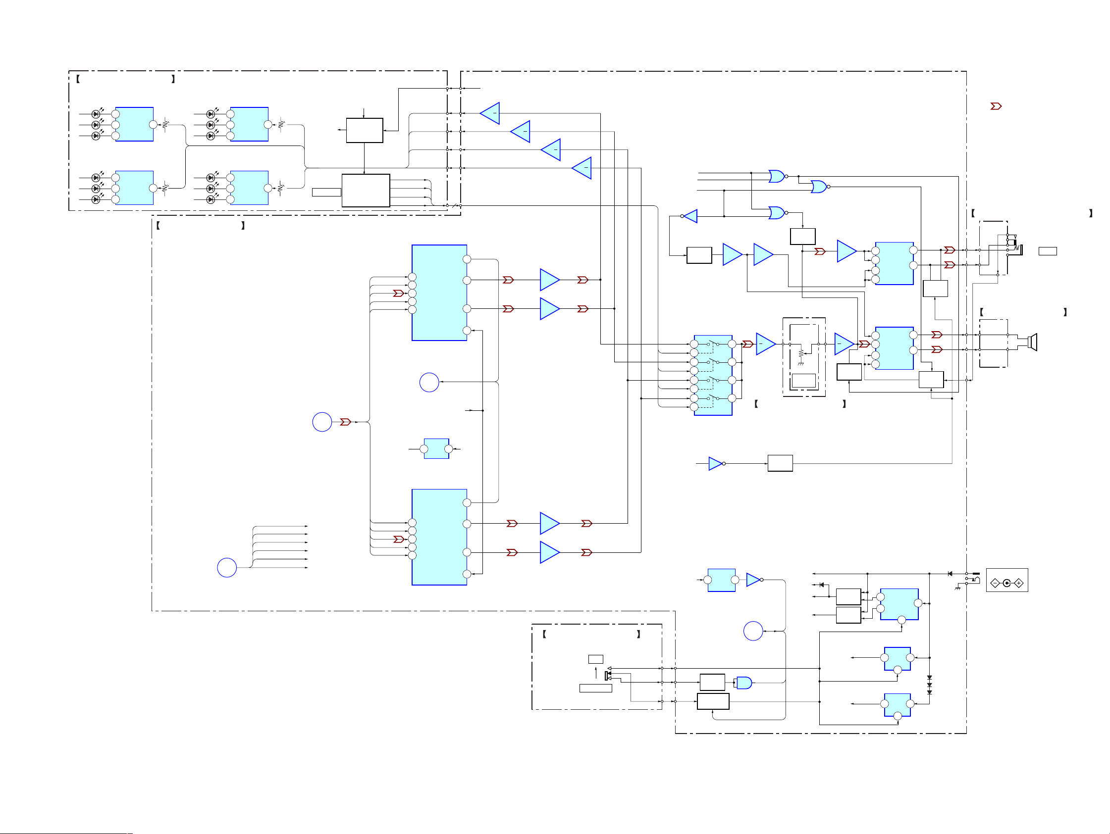
TRK-
MOD
MD BOARD
I-V AMP
IC22
3
1
75
IC23
3
75
II
J
VC
A
B
C
D
E
F
PD
Q3,4
AUTOMATIC
POWER
CONTROL
IC13
1
4
2
VS
IC24
SUM
1
4
1
3
RF MATRIX AMP
1
J
2
VC
3
A
4
B
5
C
6
D
7
E
8
F
9
PD
10
11
APC
IC14
4
FOCUS/TRACKING COIL DRIVER
SPINDLE MOTOR DRIVER
24
RO4
8
FO1
11
RO1
29
FO3
26
RO3
LDON
IC15
1
4
2
IC37
RI4
19
FI1
6
5
RI1
FI3
31
32
RI3
PS
CLK
3
34
XRST XRST
IC21
2
FFDR
FRDR
TFDR
TRDR
FS4
VREF
PEAK
BOTM
ABCD
AUX
ADFG
APCREF
SWDT
SCLK
XLAT
XSHOCK
LMOD
LPF,PHASE SHIFT
3
2
21
38
RF
37
36
35
33
32
SE
28
12
FE
34
TE
26
16
17
18
IC17
1
5
IC26
2
2
SPSW
1
6
4
7
9
10
SPFD
7
FGSV
6
Q11-14
OVER WRITE
HEAD DRIVER
7
IC12
24
IC9
6
1
7
IC10
6
1
7
IC35
LPF
14
IC34
SHOCK DETECT
2
1
1
14
2
13
Q6-8
B+
SWITCH
CHUT
IC33
6
7
4
LMOD
XSHOCK
+2.8V REG
1
5
IC29
DRIVER
2
18
Y1
3
17
I2I1Y2
8
12
I7Y7
9
11
I8G2Y8
19
EFM/ACIRC ENCODER/DECODER
69
VC
RFI
58
PEAK
64
BOTM
65
ABCD
66
AUX1
68
ADFG
82
SE
76
LDDR
84
FE
67
IC36
TE
77
1
IC20
4
2
SPFD
94
FFDR
FRDR
TFDR
TRDR
FS4
IC39
SPFD
87
FFDR
89
FRDR
86
TFDR
85
TRDR
90
FS4
32
6
3
XMGON
Q15,16
RF MOD
SWITCH
IC28
IC38
DSP,
5
4
1
2
VCC
WRPWR
EFMO
DTI
DTO
C2PO
BCK
LRCK
REC
FOK
SENS
SQSY
COUT
SRDT
XTAI
XTAO
SPRD
SWDT
SCLK
XLAT
XRST
UNREG
• Signal Path
: PB
IC2
MD MECHANISM
CONTROLLER
79
45
29
30
31
32
33
24
12
14
99
11
93
99
10
16
DTI
DTO
C2PO
BCK
LRCK
2
6
35
X1
25.4MHz
34
SPDL
DIR
8
Q9
TEMP
SENSOR
REC
FOK
SENS
WRPWR
SQSY
TCNT
SRDT
X2
10MHz
IC18
7
1
5
FGDR
6
SPSW
FGSV
AD1
AD2
80
81
AD3
CSV
60
PS2
58
PS0
82
P74
P75
83
87
IRQ0
88
IRQ1
PA3
96
15
RXD1
66
EXTL
XTL
67
P45
24
23
P44
TCA4
4
13
TXD1
17
CLK1
P94
16
PB4
6
IRQ3
90
LDON
PB7
9 63
MLON
PB5
7
IC5
4
1
2
8
PB6
RECS
5
PB3
TXD0
RXD0
D0-D7 D0-D7
A0-A15 A0-A15
XRD
XWR XWE
CSO
P42
P41
P40
PS1
P43
IRQ2
TCA0
PA0
TCKB
PA1
TCA3
PA7
PA6
PA4
RES
1
12
14
27-34
36-43
45-52
70
71
91
20
19
18
59
21
89
95
93
3
94
2
100
99
97
IC6
RESET
TXD
RXD
XRST
3
VS
DIR
PVCC
IC3
EEPROM
DAT
3
SCK
4
CS
1
XRST2
UNREG
FLASH MEMORY
21-23
25-29
20-13
3,2,31
1,12,4
5,11
32
XOE
7
XCE
30
DSCPRO
RFLCT
DISCIN
EJECT
LIMIT
MOB
CK
OEB
CW
STOP
FG
STBY
IC1
IC11
DTI
4
IC40
4
BUM-F1 BOARD
S301
S302
S303
S304
PVCC
5V
MVCC
3.5V
VCC
3.5V
1
2
1
2
SPINDLE MOTOR DRIVER
3
3
+3.5V REG
3
+3.5V REG
IC302
20
COM
16
VS
U
VS
BK–
FG
STBY
IC301
MOB
CK
OEB
CW
STOP
IC19
IC30
IC4
15
V
13
W
10
A1
13
B1
17
B2
19
A2
15
2
2
2
6
22
1
2
SLED MOTOR DRIVER
27
28
4
3
1
Q5
SWITCH
4
+5V REG
Q10
SWITCH
4
Q1
SWITCH
4
UNREG
UNREG
XRST2
(6.4V)
Q301-302
MOTOR
DRIVER
C2PO
LRCK
BCK
DTO
DTI
RECS
TXD
RXD
XRST
D6.4V
VU
W
M
M
(SPINDLE)
M903
(EJECT)
M902
(SLED)
M901
MAIN BOARD (3/3)
P
2828
Page 29
I/O SECTION
MDCT-1000
LEVEL METER BOARD
IC9201
D9201-9203
D9204-9206
LED LEVEL
METER DRIVER
VC5
9
IN
VC3
4
VC1
1
IC9202
LED LEVEL
METER DRIVER
VC5
9
IN
VC3
4
VC1
1
D9207-9209
MON LEV 1
12
D9210-9212
12
MON LEV 2
MAIN BOARD (1/3)
MAIN BOARD (3/3)
IC9203
LED LEVEL
METER DRIVER
VC5
9
VC3
4
VC1
1
IC9204
LED LEVEL
METER DRIVER
VC5
9
VC3
4
VC1
1
C
IN
12
IN
12
MON LEV 4
MAIN BOARD (2/3)
XDEM
MODE0
MODE1
XMUTE
BEEP ON
2CH X4CH
MON LEV 3
D9207
-9212
MONITOR
A
XDEM
MODE0
MODE1
XMUTE
BEEP ON
2CH X4CH
A5V
Q9201-9203
B+ SWITCH
S9201,D9215-9219
MONITOR
SELECTOR
MCLK
XPD
DADT12
LRCK
SCLK
MAIN BOARD (2/3)
MCLK
XPD
DADT34
LRCK
SCLK
MON SEL 1
MON SEL 2
MON SEL 3
MON SEL 4
17
20
12
10
11
3.3V
(IC105)
(IC305)
17
20
12
10
11
2CH X4CH
MON LEV 1
MON LEV 2
MON LEV 3
MON LEV 4
4
IC105
AD/DA CONVERTER
SDTO
MCKI
AOUTL
XPD
STDI
LRCK
AOUTR
SCLK
DEM0
ADDT12
B
XDEM
IC703
+3.3V
3
2
REG
IC305
AD/DA CONVERTER
SDTO
MCKI
AOUTL
XPD
STDI
LRCK
AOUTR
SCLK
DEM0
13
22
23
15
,ADDT34
A5V
13
22
23
15
2CH X4CH
ADDT12
21
ADDT34
IC107
AMP
67
IC307
21
AMP
IC106
BUFFER
57
31
IC306
BUFFER
57
31
SWITCH BOARD (2/2)
S9401
STANDBY
• Signal Path
: PB
67
ON
MODE0
MODE1
BEEP ON
11 12
MON SEL 1
MON SEL 2
MON SEL 3
MON SEL 4
XMUTE
IC705(1/2)
Q701
SWITCH
IC501
MONITOR SWITCH
13
5
12
6
IC705(2/2)
9
B12V
2 8
MAIN BOARD (3/3)
Q1002
SWITCH
Q1003,1004
SWITCH
IC706(1/2)
BEEP OSC
2
8
IC1002
RESET
12
34
1110
98
1
2
6
5
9
8
IC706(2/2)
BUFFER
57
1
BEEP
IC505
AMP
21
VOLUME BOARD(2/2)
IC1006
2
4
D
REG ON
IC1063
XSTANDBY
4
XPDOWN
Q502
SWITCH
NMI
IC704
4
10
Q508,510
MUTING
RV6002
MONITOR
VOL
B12V
D5VCPU
D5V
D6.4V
2
3
D1006
1
IC506(2/2)
BUFFER
31
IC506(1/2)
AMP
67
Q509,510
MUTING
Q1005
SWITCH
Q1006
SWITCH
A9V
A5V
MUTE SP1
IC509
EARPHONE AMP
IN+1
OUT1
3
IN+2
5
OUT2
IN-1
2
IN-2
6
IC507
POWER AMP
B+IN
OUTA
6
A+IN
7
OUTB
B-IN
5
A-IN
8
IC1064
SWITCHING REG
10
OUT1
VCC
7
OUT1
CTL
14
IC701
+9V
4
REG
1
IC702
+5V
4
REG
1
2
2
1
7
1
3
9
XMUTE SP0
Q514,515
MUTING
Q506,507
MUTING
D1007
FOOT SWITCH BOARD (2/2)
J9001
EAR
AUDIO I/O BOARD
(SPEAKER)
J1001
DC IN 12V
2929
Page 30

MDCT-1000
FIFO SECTION
MAIN BOARD(2/3)
MAIN BOARD
(1/3)
MAIN BOARD
(1/3)
B
3.3V
DADT12
A
DADT34
MCLK
SCLK
XPD PD
MAIN BOARD
(3/3)
+3.3V REG
18
17
15
13
11
4
F
ADDT12
IC1069
IC1027
BUFFER
1Y
2Y
4Y
6Y
8Y
IC1032
ADDT34
1A
2A
4A
6A
8A
2
IC1046
1
2
XRES1
D5V
23
2
3
256Fs
5
64Fs
7
LRCKALRCK
9
MAIN BOARD
(3/3)
E
IC1055
1
2
XRES1
4
4
+5V
+5V
DADT12r
512fs
128fs
X64fs
LRCKA
DADT34r
512fs
128fs
X64fs
LRCKA
Q1011,1013-1015
Q1012,1016-1018
ENCODER/DECODER
33
DODT12
34
AIDT12
19
XRST
EXTAL
15
ACLK
25
BCK
36
38
LRCK12
ENCODER/DECODER
33
DODT34
34
AIDT34
19
XRST
EXTAL
15
ACLK
25
BCK
36
38
LRCK34
XLAT1A
XLAT2A
B+ SWITCH
B+ SWITCH
IC1042
ATRAC
IC1051
ATRAC
ACDI12
ACDO12
XIRQ0
SCLK
SWDT
XLAT
XARQ12N
XABS12
ACDI34
ACDO34
XIRQ0
SCLK
SWDT
XLAT
XARQ34N
XABS34
IC1050
1
2
4
28
31
10
20
23
24
32
29
28
31
10
20
23
24
32
29
4
XLAT2G
IC1070
XIRQ0
SCLK
SWDT
XLAT1A
XIRQ0
SCLK
SWDT
2
1
XRES
D5V
CPU
4
4
XRES
XREC
9
10
13
IC1048
IC1047
XREC
IC1057
IC1056
12
3
2
6
1
9
10
13
12
3
2
6
1
IC1018
OSCILLATOR
2
X1003
45.1584MHz
24
24
IC1043
IC1052
G
8
11
1
XPB
2
4
XREC
5
8
11
1
XPB
2
4
XREC
5
4
MAIN BOARD
(3/3)
Q1CLK1
ADT04
63
58
ADTI2
XRQ2
57
XRQ0
64
XLAT0
62
59
XLAT2
DO12
55
DO34
69
ADTO1
53
ADTI3
94
XRQ3
95
XRQ1
96
XLAT1
52
XLAT3
93
IC1019
DIVIDER
53
512fs
A[0]-A[4]
41,38-35
A0-A4
FIFO CONTROLLER
IC1021
Q2CLK2
I/O0-I/O7
256FS
65
911
256fs
23-30
D[8]-D[15]
CS
XRD
XWR
CPUSCK
XRST
FIA0
FIA7
XRDF0
XWRFA
FIB0
FIB7
XRDF1
XWRFB
ACLK
FS64
BCK
BFIN
BFOUT
FS01
LRCK
X64fs
34
43
44
46
45
81
88
80
79
48
70
76
49
47
5
3
97
8
9
4
98
IC1020
XCS7
XRD
XHWR
16MHz
24
DATA BUS D[0]-D[15]
ADDRESS BUS A[0]-A[20]
CONTROL SIGNAL BUS
XRES
26
IC1022
128fs
64fs
LRCKA
XARQ12N
XARQ24N
64fs
X64fs
FIA[0]-FIA[7]
FIB[0]-FIB[7]
XCS3
XRD
XHWR
XLWR
14
XRAS
XOE
29
13
XWE
30
XUCAS
XLCAS
31
10,11,13
14,19-22
18
XR
2
XW
10,11,13
14,19-22
18
XR
2
XW
IC1059
7 15
Ep RCo
CK
2
1
XCLR
IC1060
7 15
Ep RCo
CK
2
1
XCLR
IC1062
24
IC1017
DRAM
IC1025
FIFO
Q0
Q7
PB
1/2ch
IC1026
FIFO
Q0
Q7
PB
3/4ch
COUNTER
I/O0
I/O15
A0
A8
A9
A11
D0
D7
D0
D7
XRS
XRS
2-5,7-10
33-36
38-41
17-20
23-27
28,16
15
7-4
31-28
25
7-4
31-28
25
IC1061(1/2)
12
D2
CLK2
11
13
CLR2
IC1061(2/2)
2
D1
CLK1
3
1
CLR1
D[0]-D[15]
A[1]-A[9]
A[18]-A[20]
D[8]-D[15]
D[8]-D[15]
8
XQ2
6
XQ1
XRES1
FINT12
FINT34
RST01
L
H
I
J
MAIN BOARD
K
MAIN BOARD
(3/3)
• Signal Path
: PB
MAIN BOARD
(3/3)
(3/3)
3030
Page 31

CPU SECTION
MDCT-1000
SWITCH
BOARD
FOOT SWITCH
BOARD (1/2)
MAIN BOARD (3/3)
DATA BUS D[0]-D[15]
ADDRESS BUS A[0]-A[20]
CONTROL SIGNAL BUS
IC1014
1
XRESL
XRES
IC1010
45-52
54-65,95
A0-A20
Q1007
SWITCH
Q1008
SWITCH
Q1009
SWITCH
Q1010
SWITCH
8
R1IN
T1OUT
13
IC1003
NVRAM
IC1005
SCLK
DO
CS
R1OUT
DI
AN-IN[1]
AN-IN[3]
AN-IN[5]
AN-IN[6]
TRC_ON
AN-IN[0]
AN-IN[7]
T1IN
2
4
3
1
SW_AN-IN1
SW_AN-IN3
M
SW_AN-IN5
SW_AN-IN6
SW_SLA
SW_SLB
TRC_ON
FS_PLAY
FS–FS
N
FS-BS
B12V
RX232C
TX232C
B12V
SLA
SLB
11
9
87
AN-IN1
AN-IN3
89
91
AN-IN5
92
AN-IN6
PB0
2
PB1
3
4
PB2
KEY-IN
86
AN-IN7
93
22
RXD0
TXD0
20
PA2(NV_SCLK)
107
PA3(NV_DIO)
108
PA5(NV_CS)
110
IC1007
CPU
27-34
36-43
XRD
D0-D15
XHWR
XLWR
XCS0
XCS1
XCS3
XCS4
XCS6
XCS7
PA4(XREST)
PA7(1809RST)
IRQ0
XDREQ0
XDREQ1
KEY-INT
PHA1
XTAL
EXTAL
XRES
NMI
PB4
PBF5
XRES_AD
XRES1
FINT12
FINT34
78
79
80
104
103
101
13
15
16
109
111
100
17
69
75
74
71
72
68
67
18
102
8
9
6
7
XRD
XHWR
XLWR
XCS0
XCS1
XCS3
XCS4
XCS6
XCS7
XRESL
1809RST
IRQ0
XDREQ0
XDREQ1
INT1809
IC1009
1
2
X1002
16MHz
XSTANDBY
XPDOWN
XRES1
FINT12
FINT34
NMI
PD
4
16MHz
IC1008
RESET
1 2
XCS0
XRD
XCS1
XRD
XHWR
XCS1
XRD
XLWR
D
E
L
EPROM
D8-D15
D0-D7
2
XCE
A0-A17
20
XRD
IC1016
SRAM
XCE
20
XOE
22
A0
XWE
27
A14
IC1067
SRAM
XCE
20
XOE
22
A0
XWE
27
A14
D5VCPU
MAIN BOARD (1/3)
MAIN BOARD (2/3)
MAIN BOARD (2/3)
D0
D7
D0
D7
10-3
19-12
21-29
31-39
11-13
15-19
10-3,25
24,21
23,2,1
11-13
15-19
10-3,25
24,21
23,2,1
D[0]-D[15]
A[1]-A[18]
D[8]-D[15]
A[1]-A[15]
D[0]-D[7]
A[1]-A[15]
MAIN BOARD (1/3)
D[8]-D[15]
XRD
XCS4
16MHz
XRES
A[0]
XRD
XHWR
XCS4
16MHz
XRES
16MHz
D[0]-D[15]
A[1]-A[5]
16MHz
1809RST
XCS6
XLWR
XHWR
XRD
XDREQ0
XDREQ1
INT1809
IRQ0
C
XDEM
2CH X4CH
MODE1
MODE0
XMUTE
BEEP ON
4
2
IC1011
BUS TRANSCEIVER
1A
2
8A
9
1
DIR
IC1012
1
4
2
IC1013
BUFFER
1A
2
2A
3
3A
4
5
4A
6
5A
9
8A
IC1071
1
2
1D 1Q
2
3
1CK
32-37
39-48
15
19
4
5
7
8
9
10
12
14
30
31
60
59
58
57
56
55
1B
8B
IC1015
D-FF
1D 1Q
2
3
1CK
4
1XS
1Y
2Y
3Y
4Y
5Y
8Y
4
IC1072
D-FF
5
TIMING
CONTROL
MD CONTROLLER
HD00
HD15
HAD1
HAD5
HSCK
XRST
HXCS
HXWL
HXWH
HXRD
HXD0
HXD1
HXI1
HXI2
IO07
IO06
IO05
IO04
IO03
IO02
18
11
5
18
17
16
15
14
11
12 9
11
IC1033
DISP_CTL
LCD-D08-D15
DIRECTION
CONTROL
2D 2Q
2CK
RA07
RA08
DTOT
DTIN
C2PO
LRCK
BTCK
RCTR
SDIN
SDOT
RD02
RA04
RA07
RA06
RD00
RD01
RD04
RD05
LCD A[0]
LCD XRD
LCD XHWR
LCD XCS4
LCD 16MHz
LCD XRES
79
80
90
91
92
93
94
95
49
50
64
74
69
68
61
62
66
67
8
RST01
XIRQ0
XREC
XPB
SCLK
SWDT
XLAT1A
XLAT2A
O
DECKSEL
XMDRES
DTOT-1809
DTIN-1809
C2PO-1809
LRCK-1809
BTCK-1809
RCTR-1809
SDIN-1809
SDOT-1809
LCD BOARD
SDDT-1809
DECKSEL
DTOT-1809
RCTR-1809
C2PO-1809
SDIN-1809
LRCK-1809
DECKSEL
BTCK-1809
DTIN-1809
XMDRES
DECKSEL
K
MAIN BOARD (2/3)
F
H
MAIN BOARD (2/3)
I
J
IC1037
2
IC1036
2
1
MAIN BOARD (2/3)
• Signal Path
: PB
IC1038
1
4
2
4
4
IC1039
1
4
2
IC1040
1
4
2
IC1034
4
7
9
12
1
IC1035
4
7
11
10
14
13
6
(L=A ,H=B)
+3.3V D5VCPU
XRES
G
RXD A
DTI A
RECS A
2
3
C2PO A
5
6
11
10
14
13
12
TXD A
LRCK A
BCK A
2
3
DTO A
5
6
XRST A
9
IC1065
+3.3V
3
REG
MAIN BOARD (2/3)
RECS A
C2PO A
TXD A
RXD A
LRCK A
BCK A
DTO A
DTI A
XRST A
D6.4V
2
P
MD BOARD
3131
Page 32

MDCT-1000
LCD SECTION
MAIN BOARD
(3/3)
O
8
LCD
16MHz
LCD BOARD
DISP_CTL
LCD-D08-D15
LCD-A0[0]
LCD-XRD
LCD-XHWR
LCD-XCS4
LCD-XRES
IC4012(2/2)
COUNTER
2D
12
2CK
11
33
30
40
36
37
35
49-42
6-1
59-50
7
9
8
YDIS
DIN
FR
LP
XSCL
VA15
VA14
VA13
VA10
VA15
VA14
VA13
VA12
IC4001(1/2)
12
10
9
IC4001(2/2)
1
2
4
5
XD0-XD3
FR
IC4006
VRAM
VD0-7
VA0-15
IC4002
8
10
9
8
6
11
12
3
1
2
13
11-13
D0-7
15-19
10-3,25
24,21,23
A0-15
2,26,1
27
XWE
22
XOE
5
4
20
6
XCE
8MHz
XSCL
XSCL
LP
IC4008
8
LP
9
11
LP
12
IC4007
D-FF
2
1D
1Q
3
1CK
10
13
5
TIMING GENERATOR
IC4010
COUNTER
9
XLD
7
EP
CK
2
(DCBA)
=(0000)
IC4011
COUNTER
9
XLD
ET
10
7
EP
CK
2
(DCBA)
=(1010)
RCO
RCO
IC4012(1/2)
D-FF
5
1Q
1Q
2
1CK
3
6
1Q
15
D5V
15
XSCL
YDIS
LOAD LOAD0
DIN
YDIS
IC4014
+3.3V
2 3
REG
IC4013
+3.0V
REG
IC4015,Q4001
DC/DC
CONV
IC4004
LCD CONTROLLER
XD0
XD3
22
D0
29
D7
A0
20
XRD
13
14
XWK
19
XCS
10
XRCS
8MHz
8MHz
17
XG
9
2Q
8
2Q
YD
WE
LP
XSCL
VD0-7
VA0-15
XVWR
XVRD
XVCE
IC4016
BUFFER
7Y
12
4Y
15
18
1Y
16
3Y
8Y
11
2Y
17
4
Q4002,
Q4003
D0-D3
DF
CP
DISP
FRAME
VD1
VD2
LCD VDD
LCD VCC
LCD VSS
4
LCD
UNIT
7A
8
4A
5
2
1A
4
3A
8A
9
2A
3
IC4017
1
2
32
SWITCH
SWITCH BOARD (1/2)
S5001,5003-5005
FUNCTION SWITCH
S5016
FUNCTION SWITCH
S5032-5037
FUNCTION SWITCH
S5038
FUNCTION SWITCH
S5041
INDEX
SEARCH
/SELECT
ROTARY
ENCODER
SW_AN-IN1
SW_AN-IN3
SW_AN-IN5
SW_AN-IN6
SW_SLA
SW_SLB
M
MAIN BOARD
(3/3)
CONTROL
UNIT
FOOT SWITCH BOARD (1/2)
FS_PLAY IN
FS_FS
FS_BS
FL8001
FL
B12V
N
MAIN BOARD
(3/3)
RV6001
LCD CONTRAST
VOLUME BOARD
+–
3232
Page 33

MDCT-1000
5-
)11(
005
901RIT
UPBLOCK
50
5-3. PRINTED WIRING BOARD MD SECTION
• : Uses unleaded solder.
MD BOARD
• See page 27 for Circuit Boards Location.
PTICA
PICK-
KMS-2
• Semiconductor
Location
Ref. No. Location
D1 H-6
D3 I-7
D6 F-3
D7 E-8
D8 E-7
D9 E-8
D10 E-7
HR
VER W
IC1 F-7
IC2 G-5
IC3 H-4
IC4 H-5
IC5 I-8
IC6 I-7
IC9 E-6
IC10 E-5
IC11 I-4
IC12 D-2
IC13 B-6
IC14 B-6
IC15 B-6
IC17 E-1
IC18 D-1
IC19 H-2
IC20 B-5
IC21 D-6
IC22 A-7
IC23 A-6
IC24 A-5
IC26 E-3
IC28 D-7
IC29 D-8
IC30 G-8
IC33 C-4
IC34 C-5
IC35 C-5
IC36 E-4
IC37 F-2
IC38 B-3
IC39 A-4
IC40 H-4
Q1 I-6
Q3 B-6
Q4 B-7
Q5 H-2
Q6 A-5
Q7 A-5
Q8 A-4
Q9 H-3
Q10 G-7
Q11 D-8
Q12 D-7
Q13 F-7
Q14 F-8
Q15 A-5
Q16 B-5
A
TO
CN301
BUM-F1 BOARD
1-674-22
TO
MAIN BOARD
N1
3333
Page 34

MDCT-1000
5-4. SCHEMATIC DIAGRAM MD SECTION (1/4)
• See page 73 for IC Block Diagrams.
IC B/D
IC B/D
IC B/D
IC B/D
IC B/D
IC B/D
3434
Page 35

MDCT-1000
5-5. SCHEMATIC DIAGRAM MD SECTION (2/4)
• See page 69, 73 for IC Block Diagrams.
IC B/D
IC B/D
3535
Page 36

MDCT-1000
5-6. SCHEMATIC DIAGRAM MD SECTION (3/4)
• See page 27 for Waveform. • See page 70 for IC Block Diagram.
IC B/D
9
3636
Page 37

MDCT-1000
5-7. SCHEMATIC DIAGRAM MD SECTION (4/4)
• See page 27 for Waveform.
3737
Page 38

MDCT-1000
5-8. SCHEMATIC DIAGRAM BUM SECTION
• See page 72 for IC Block Diagrams.
IC B/D
IC B/D
3838
Page 39

MDCT-1000
5-9. PRINTED WIRING BOARD BUM SECTION
• : Uses unleaded solder.
• See page 27 for Circuit Boards Location.
(LOADING)
IC301
A
MD BOARD
CN5
IC302
3939
Page 40

MDCT-1000
5-10. SCHEMATIC DIAGRAM MAIN SECTION (1/11)
4040
Page 41

5-11. SCHEMATIC DIAGRAM MAIN SECTION (2/11)
MDCT-1000
4141
Page 42

MDCT-1000
5-12. SCHEMATIC DIAGRAM MAIN SECTION (3/11)
4242
Page 43

MDCT-1000
5-13. SCHEMATIC DIAGRAM MAIN SECTION (4/11)
• See page 73,75 for IC Block Diagrams.
IC B/D
IC B/D
4343
Page 44

MDCT-1000
5-14. SCHEMATIC DIAGRAM MAIN SECTION (5/11)
• See page 27 for Waveform. • See page 66 for IC Pin Function Description.
4444
Page 45

5-15. SCHEMATIC DIAGRAM MAIN SECTION (6/11)
MDCT-1000
4545
Page 46

MDCT-1000
5-16. SCHEMATIC DIAGRAM MAIN SECTION (7/11)
• See page 27 for Waveform. • See page 67 for IC Pin Function Description.
4646
Page 47

MDCT-1000
5-17. SCHEMATIC DIAGRAM MAIN SECTION (8/11)
• See page 75 for IC Block Diagrams.
IC B/D
IC B/D
4747
Page 48

MDCT-1000
5-18. SCHEMATIC DIAGRAM MAIN SECTION (9/11)
• See page 74 for IC Block Diagram.
IC B/D
4848
Page 49

5-19. SCHEMATIC DIAGRAM MAIN SECTION (10/11)
MDCT-1000
4949
Page 50

MDCT-1000
5-20. SCHEMATIC DIAGRAM MAIN SECTION (11/11)
• See page 75 for IC Block Diagram.
IC B/D
5050
Page 51

MDCT-1000
5-21. PRINTED WIRING BOARD MAIN SECTION
MAIN BOARD
A
B
C
FOOT SWITCH
D
E
F
G
H
I
J
L
TO
BOARD
CN8001
F
TO
LCD BOARD
CN4001
B
TO
MD BOARD
CN2
12
CN1002
CN1005
TO 1/4 TO 2/4
CN1004
345678910111213
• : Uses unleaded solder.
• See page 27 for Circuit Boards Location.
CN1001
SWITCH BOARD
TO
K
CN5001
CN112
CN115
12
N
TO
AUDIO I/O
BOARD
CN9103
J
TO
VOLUME
BOARD
CN6002
• Semiconductor Location
Ref. No. Location
D501 C-13
D701 D-11
D702 A-6
D703 B-5
D704 C-5
D1004 C-4
D1005 C-4
D1006 H-3
D1007 A-4
D1008 B-3
IC105 D-9
IC106 D-9
IC107 F-12
IC305 D-7
IC306 C-9
IC307 E-12
IC501 D-11
IC505 C-10
IC506 B-11
IC507 A-12
IC509 D-12
IC701 A-6
IC702 C-5
IC703 E-8
IC704 D-12
IC705 D-12
IC706 D-11
Ref. No. Location
IC1036 F-3
IC1037 E-3
IC1038 F-3
IC1039 F-3
IC1040 F-3
IC1042 I-10
IC1043 I-11
IC1046 I-11
IC1047 I-11
IC1048 I-11
IC1050 H-10
IC1051 G-10
IC1052 H-12
IC1055 G-11
IC1056 G-11
IC1057 G-11
IC1059 H-10
IC1060 H-11
IC1061 H-11
IC1062 H-10
IC1063 B-2
IC1064 B-4
IC1065 D-3
IC1067 F-6
IC1069 F-8
IC1070 I-10
IC1071 D-4
IC1072 D-5
IC1002 C-3
IC1003 J-5
IC1005 H-6
IC1006 B-3
M
TO
FOOT
SWITCH
CN109
BOARD
CN9001
CN114
TO 4/4TO 3/4
IC1007 H-5
IC1008 I-2
IC1009 H-3
IC1010 G-5
IC1011 E-5
IC1012 E-5
IC1013 D-4
IC1014 E-5
IC1015 D-5
E
TO
LEVEL
METER
BOARD
CN9201
IC1016 F-7
IC1017 G-7
IC1018 I-6
IC1019 H-7
IC1020 H-7
IC1021 H-7
IC1022 H-9
IC1025 G-8
IC1026 H-9
1-680-430-
11
(11)
IC1027 G-9
IC1032 G-8
IC1033 F-4
IC1034 F-4
IC1035 F-3
Q502 D-13
Q506 D-12
Q507 B-12
Q508 C-11
Q509 A-12
Q510 D-11
Q514 C-12
Q515 C-13
Q701 D-11
Q1002 B-3
Q1003 B-4
Q1004 B-4
Q1005 B-4
Q1006 B-3
Q1007 C-3
Q1008 C-3
Q1009 C-3
Q1010 C-3
Q1011 H-10
Q1012 G-10
Q1013 I-10
Q1014 H-10
Q1015 I-10
Q1016 G-10
Q1017 G-10
Q1018 G-10
5151
Page 52

MDCT-1000
5
3
7
2
4
8
1
001
C
D
O
6
OOT S
CH
MAIN SECTION (1/4)
L
TO
F
WIT
BOARD
CN8001
L
MD B
• : Uses unleaded solder.
MAIN BOARD
F
TO
D BOAR
CN4001
B
TO
ARD
CN2
• See page 27 for Circuit Boards Location.
J1001
DC IN 12V
1
IC 100
113
70
70
70
70
70
71
• Semiconductor Location
Ref. No. Location Ref. No. Location
D501 C-13
D701 D-11
D702 A-6
D703 B-5
D704 C-5
D1004 C-4
D1005 C-4
D1006 H-3
D1007 A-4
D1008 B-3
IC105 D-9
IC106 D-9
IC107 F-12
IC305 D-7
IC306 C-9
IC307 E-12
IC501 D-11
IC505 C-10
IC506 B-11
IC507 A-12
IC509 D-12
IC701 A-6
IC702 C-5
IC703 E-8
IC704 D-12
IC705 D-12
IC706 D-11
IC1002 C-3
IC1003 J-5
IC1005 H-6
IC1006 B-3
IC1007 H-5
IC1008 I-2
IC1009 H-3
IC1010 G-5
IC1011 E-5
IC1012 E-5
IC1013 D-4
IC1014 E-5
IC1015 D-5
IC1016 F-7
IC1017 G-7
IC1018 I-6
IC1019 H-7
IC1020 H-7
IC1021 H-7
IC1022 H-9
IC1025 G-8
IC1026 H-9
IC1027 G-9
IC1032 G-8
IC1033 F-4
IC1034 F-4
IC1035 F-3
IC1036 F-3
IC1037 E-3
IC1038 F-3
IC1039 F-3
IC1040 F-3
IC1042 I-10
IC1043 I-11
IC1046 I-11
IC1047 I-11
IC1048 I-11
IC1050 H-10
IC1051 G-10
IC1052 H-12
IC1055 G-11
IC1056 G-11
IC1057 G-11
IC1059 H-10
IC1060 H-11
IC1061 H-11
IC1062 H-10
IC1063 B-2
IC1064 B-4
IC1065 D-3
IC1067 F-6
IC1069 F-8
IC1070 I-10
IC1071 D-4
IC1072 D-5
Q502 D-13
Q506 D-12
Q507 B-12
Q508 C-11
Q509 A-12
Q510 D-11
Q514 C-12
Q515 C-13
Q701 D-11
Q1002 B-3
Q1003 B-4
Q1004 B-4
Q1005 B-4
Q1006 B-3
Q1007 C-3
Q1008 C-3
Q1009 C-3
Q1010 C-3
Q1011 H-10
Q1012 G-10
Q1013 I-10
Q1014 H-10
Q1015 I-10
Q1016 G-10
Q1017 G-10
Q1018 G-10
5252
Page 53

MDCT-1000
5
O
D
03
O
E
D
6002
C
013
MAIN SECTION (2/4)
• : Uses unleaded solder.
• See page 27 for Circuit Boards Location.
I
1
N11
T
AR
N91
T
VOLUM
AR
N
• Semiconductor Location
Ref. No. Location Ref. No. Location
D501 C-13
D701 D-11
D702 A-6
D703 B-5
D704 C-5
D1004 C-4
D1005 C-4
D1006 H-3
D1007 A-4
D1008 B-3
IC105 D-9
IC106 D-9
IC107 F-12
IC305 D-7
IC306 C-9
IC307 E-12
IC501 D-11
IC505 C-10
IC506 B-11
IC507 A-12
IC509 D-12
IC701 A-6
IC702 C-5
IC703 E-8
IC704 D-12
IC705 D-12
IC706 D-11
IC1002 C-3
IC1003 J-5
IC1005 H-6
IC1006 B-3
IC1007 H-5
IC1008 I-2
IC1009 H-3
IC1010 G-5
IC1011 E-5
IC1012 E-5
IC1013 D-4
IC1014 E-5
IC1015 D-5
IC1016 F-7
IC1017 G-7
IC1018 I-6
IC1019 H-7
IC1020 H-7
IC1021 H-7
IC1022 H-9
IC1025 G-8
IC1026 H-9
IC1027 G-9
IC1032 G-8
IC1033 F-4
IC1034 F-4
IC1035 F-3
IC1036 F-3
IC1037 E-3
IC1038 F-3
IC1039 F-3
IC1040 F-3
IC1042 I-10
IC1043 I-11
IC1046 I-11
IC1047 I-11
IC1048 I-11
IC1050 H-10
IC1051 G-10
IC1052 H-12
IC1055 G-11
IC1056 G-11
IC1057 G-11
IC1059 H-10
IC1060 H-11
IC1061 H-11
IC1062 H-10
IC1063 B-2
IC1064 B-4
IC1065 D-3
IC1067 F-6
IC1069 F-8
IC1070 I-10
IC1071 D-4
IC1072 D-5
Q502 D-13
Q506 D-12
Q507 B-12
Q508 C-11
Q509 A-12
Q510 D-11
Q514 C-12
Q515 C-13
Q701 D-11
Q1002 B-3
Q1003 B-4
Q1004 B-4
Q1005 B-4
Q1006 B-3
Q1007 C-3
Q1008 C-3
Q1009 C-3
Q1010 C-3
Q1011 H-10
Q1012 G-10
Q1013 I-10
Q1014 H-10
Q1015 I-10
Q1016 G-10
Q1017 G-10
Q1018 G-10
5353
Page 54

MDCT-1000
MAIN SECTION (3/4)
• : Uses unleaded solder.
CN2
• See page 27 for Circuit Boards Location.
• Semiconductor Location
Ref. No. Location Ref. No. Location
D501 C-13
D701 D-11
D702 A-6
D703 B-5
D704 C-5
D1004 C-4
D1005 C-4
D1006 H-3
D1007 A-4
D1008 B-3
IC105 D-9
IC106 D-9
IC107 F-12
IC305 D-7
IC306 C-9
IC307 E-12
IC501 D-11
IC505 C-10
IC506 B-11
IC507 A-12
IC509 D-12
IC701 A-6
IC702 C-5
IC703 E-8
IC704 D-12
IC705 D-12
IC706 D-11
IC1002 C-3
IC1003 J-5
IC1005 H-6
IC1006 B-3
IC1007 H-5
IC1008 I-2
IC1009 H-3
IC1010 G-5
IC1011 E-5
IC1012 E-5
IC1013 D-4
IC1014 E-5
IC1015 D-5
IC1016 F-7
IC1017 G-7
IC1018 I-6
IC1019 H-7
IC1020 H-7
IC1021 H-7
IC1022 H-9
IC1025 G-8
IC1026 H-9
IC1027 G-9
IC1032 G-8
IC1033 F-4
IC1034 F-4
IC1035 F-3
IC1036 F-3
IC1037 E-3
IC1038 F-3
IC1039 F-3
IC1040 F-3
IC1042 I-10
IC1043 I-11
IC1046 I-11
IC1047 I-11
IC1048 I-11
IC1050 H-10
IC1051 G-10
IC1052 H-12
IC1055 G-11
IC1056 G-11
IC1057 G-11
IC1059 H-10
IC1060 H-11
IC1061 H-11
IC1062 H-10
IC1063 B-2
IC1064 B-4
IC1065 D-3
IC1067 F-6
IC1069 F-8
IC1070 I-10
IC1071 D-4
IC1072 D-5
Q502 D-13
Q506 D-12
Q507 B-12
Q508 C-11
Q509 A-12
Q510 D-11
Q514 C-12
Q515 C-13
Q701 D-11
Q1002 B-3
Q1003 B-4
Q1004 B-4
Q1005 B-4
Q1006 B-3
Q1007 C-3
Q1008 C-3
Q1009 C-3
Q1010 C-3
Q1011 H-10
Q1012 G-10
Q1013 I-10
Q1014 H-10
Q1015 I-10
Q1016 G-10
Q1017 G-10
Q1018 G-10
5454
Page 55

MDCT-1000
SWITCH BOARD
CN5001
680-430-
)
O
OOT
CH
D
9001
O
D
01
013
MAIN SECTION (4/4)
• : Uses unleaded solder.
• See page 27 for Circuit Boards Location.
1-
T
F
WIT
BOAR
N
T
BOAR
N92
11
• Semiconductor Location
Ref. No. Location Ref. No. Location
D501 C-13
D701 D-11
D702 A-6
D703 B-5
D704 C-5
D1004 C-4
D1005 C-4
D1006 H-3
D1007 A-4
D1008 B-3
IC105 D-9
IC106 D-9
IC107 F-12
IC305 D-7
IC306 C-9
IC307 E-12
IC501 D-11
IC505 C-10
IC506 B-11
IC507 A-12
IC509 D-12
IC701 A-6
IC702 C-5
IC703 E-8
IC704 D-12
IC705 D-12
IC706 D-11
IC1002 C-3
IC1003 J-5
IC1005 H-6
IC1006 B-3
IC1007 H-5
IC1008 I-2
IC1009 H-3
IC1010 G-5
IC1011 E-5
IC1012 E-5
IC1013 D-4
IC1014 E-5
IC1015 D-5
IC1016 F-7
IC1017 G-7
IC1018 I-6
IC1019 H-7
IC1020 H-7
IC1021 H-7
IC1022 H-9
IC1025 G-8
IC1026 H-9
IC1027 G-9
IC1032 G-8
IC1033 F-4
IC1034 F-4
IC1035 F-3
IC1036 F-3
IC1037 E-3
IC1038 F-3
IC1039 F-3
IC1040 F-3
IC1042 I-10
IC1043 I-11
IC1046 I-11
IC1047 I-11
IC1048 I-11
IC1050 H-10
IC1051 G-10
IC1052 H-12
IC1055 G-11
IC1056 G-11
IC1057 G-11
IC1059 H-10
IC1060 H-11
IC1061 H-11
IC1062 H-10
IC1063 B-2
IC1064 B-4
IC1065 D-3
IC1067 F-6
IC1069 F-8
IC1070 I-10
IC1071 D-4
IC1072 D-5
Q502 D-13
Q506 D-12
Q507 B-12
Q508 C-11
Q509 A-12
Q510 D-11
Q514 C-12
Q515 C-13
Q701 D-11
Q1002 B-3
Q1003 B-4
Q1004 B-4
Q1005 B-4
Q1006 B-3
Q1007 C-3
Q1008 C-3
Q1009 C-3
Q1010 C-3
Q1011 H-10
Q1012 G-10
Q1013 I-10
Q1014 H-10
Q1015 I-10
Q1016 G-10
Q1017 G-10
Q1018 G-10
1
5555
Page 56

MDCT-1000
5-22. SCHEMATIC DIAGRAM AUDIO SECTION
5656
Page 57

MDCT-1000
I/O BOARD
680
8-
)
OARD
5
0
3
O
MAIN BOARD
2
D
680
-
)
6002RV6001
OL
ST
OARD
002
5-23. PRINTED WIRING BOARD AUDIO SECTION
• : Uses unleaded solder.
• See page 27 for Circuit Boards Location.
N910
VOLUME BOAR
RV
1-
-42
11
N
TO
MAIN B
N11
3
1
G
TO
LCD
B
N4
T
CN11
MONITOR V
LCD CONTRA
1-
-424
11
5757
Page 58

MDCT-1000
5-24. SCHEMATIC DIAGRAM LEVEL METER SECTION
4.7 25V
4.7 25V
4.7 25V4.7 25V
5858
Page 59

MDCT-1000
O
MAIN BOARD
09
D
680
-
1
OR
L
5
6
03
02
01
0
7
8
9
5-25. PRINTED WIRING BOARD LEVEL METER SECTION
EVEL METER BOAR
• : Uses unleaded solder.
920
MONIT
AL
• See page 27 for Circuit Boards Location.
D921
D921
D92
D92
2ch MODE
D92
D921
D921
D921
D9212D9211D921
1-
-427
11
(11)
4ch MODE
• Semiconductor
Location
Ref. No. Location
D9201 C-9
D9202 C-8
D9203 C-8
D9204 D-9
D9205 D-8
D9206 D-8
D9207 F-9
D9208 F-8
D9209 F-8
D9210 G-9
D9211 G-8
D9212 G-8
D9213 D-4
D9214 D-4
D9215 A-7
D9216 C-7
D9217 D-7
D9218 F-7
D9219 G-7
T
CN1
IC9201 B-11
IC9202 C-11
IC9203 F-11
IC9204 G-11
Q9201 H-3
Q9202 H-2
Q9203 G-2
5959
Page 60

MDCT-1000
5-26. SCHEMATIC DIAGRAM LCD SECTION
10µH
• See page 71 for IC Block Diagrams.
IC B/D
8
IC B/D
6060
Page 61

MDCT-1000
O
MAIN BOARD
004
D
680-431-
)
T
013
0
5-27. PRINTED WIRING BOARD LCD SECTION
LCD BOAR
• : Uses unleaded solder.
• See page 27 for Circuit Boards Location.
G
TO
VOLUME
BOARD
CN6001
CN1
• Semiconductor
Location
Ref. No. Location
D4001 A-11
D4002 B-11
D4003 D-11
IC4001 B-2
IC4002 C-2
IC4004 C-3
IC4006 B-3
IC4007 B-6
IC4008 A-5
IC4010 C-5
2
1-
T
LCD UNI
11
1
IC4011 C-6
IC4012 C-7
IC4013 A-7
IC4014 D-5
IC4015 B-11
IC4016 E-8
IC4017 D-7
Q4001 A-10
Q4002 B-10
Q4003 C-10
Q4004 B-11
6161
Page 62

MDCT-1000
5-28. SCHEMATIC DIAGRAM SWITCH SECTION
6262
Page 63

MDCT-1000
TO
MAIN BOARD
001
680-432-
)
ON
A
CH
/
T
E
2
OP
SFF/FS
CT
E
6
B
013
5-29. PRINTED WIRING BOARD SWITCH SECTION
• : Uses unleaded solder.
504
• See page 27 for Circuit Boards Location.
FUNCTI
DISP MOD
INDEX SEAR
SELEC
T
1-
11
REW/B
PLAY/PAUS
DECK
501
EJE
CN1
DECK
1
6363
Page 64

MDCT-1000
5-30. SCHEMATIC DIAGRAM FOOT SWITCH SECTION
6464
Page 65

MDCT-1000
O
MAIN BOARD
4
680
6-
)
J9001
2
OARD
002
0
5-31. PRINTED WIRING BOARD FOOT SWITCH SECTION
FOOT SWITCH BOARD
T
• : Uses unleaded solder.
• See page 27 for Circuit Boards Location.
CONTROL UNIT
N800
CN11
MAIN
B
N1
TO
1-
-42
11
1
6565
Page 66

MDCT-1000
5-32. IC PIN FUNCTION DESCRIPTION
• IC1021 CXD8655Q (FIFO CONTROLLER) (MAIN BOARD)
Pin No.
1
2
3
4
5
6
7
8
9
10 - 14
15
16
17 - 20
21 - 22
23 - 30
31
32 - 33
34
35 - 38
39
40
41
42
43
44
45
46
47
48
49
50
51
52
53
54
55
56
57
58
59
60
61
62
63
64
65
66
67
68
69
Pin Name
INVIN
INVOUT
FS64
FS01
ACLK
FFCLK
FFOUT
BFIN
BFOUT
TEST00-04
VSS
VDD
TEST05-08
TEST10-11
I/O0-7
VDD
TEST12-13
CS
A4-1
VSS
VDD
A0
XINT
XRD
XWR
XRST
CPUSCK
XWRFB
FIB0
XRDF1
F863
AC21
XLAT1
ADTO1
MLTC
DO12
F860
XRQ2
ADTI2
XLAT2
F862
AC20
XLAT0
ADTO0
XRQ0
256FS
VSS
VDD
F861
DO34
I/O
I
Input terminal of an inverter for a general purpose
O
Output terminal of an inverter for a general purpose (open)
O
Divider output (1/4) of 256fs
O
Divider output (1/256) of 256fs
O
Clock output (128fs) for data communications with ATRAC CODEC
I
Not used (connected to ground)
O
Not used (open)
I
Input terminal of a buffer for a general purpose (64fs)
O
Output terminal of a buffer for a general purpose (64fs)
I
Not used (connected to ground)
—
Ground
—
Power supply (+5V)
I
Not used (connected to ground)
O
Not used (open)
I/O
Data bus
—
Power supply (+5V)
O
Not used (open)
I
Chip select signal input
I
Address bus from the CPU
—
Ground
—
Power supply (+5V)
I
Address bus from the CPU
O
Not used
I
Read signal input from the CPU
I
Write signal input from the CPU
I
Reset signal input from the CPU
I
System clock input from the CPU (16MHz)
O
Write signal output for the FIFO (PLAY 3/4ch)
I/O
Input/output terminal of data communications with the FIFO (3/4ch)
O
Read signal output for the FIFO (PLAY 3/4ch)
I
Not used (connected to ground)
O
Not used (open)
O
Latch signal output for transferring serial data (ADTO1) to the ATRAC CODEC (3/4ch) during PLAY operation
O
Serial data output to the ATRAC decoder (3/4ch)
I
Input terminal for multi-chip setting (connected to ground for single-chip setting)
I
Input teminal of 1/2ch digital audio data
I
Not used (connected to ground)
I
Request signal input to receive serial data from the ATRAC encoder during REC operation
I
Serial data input from the ATRAC encoder (1/2ch)
O
Strobe signal output for receiving serial data (ADTI2) from the ATRAC CODEC (1/2ch) during REC opeation
I
Not used (connected to ground)
O
Not used (open)
O
Latch signal output for transferring serial data (ADTO0) to the ATRAC CODEC (1/2ch) during PLAY operation
O
Serial data output to the ATRAC decoder (1/2ch)
I
Request signal input to send serial data from the ATRAC decoder (1/2ch) during PLAY operation
I
Clock input (256fs)
—
Ground
—
Power supply (+5V)
I
Not used (connected to ground)
I
Input terminal of 3/4ch digital audio data
Description
Pin No.
70 - 76
77
78
79
80
81 - 88
89
90
91
92
93
94
95
96
97
98
99
100
Pin Name
FIB1-7
XWRF3
XRDFB
XWRFA
XRDF0
FIA0-7
XWRF2
VSS
VDD
XRDFA
XLAT3
ADTI3
XRQ3
XRQ1
BCK
LRCK
VSS
NC
I/O
I/O
Input/output terminal of data communications with the FIFO (3/4ch)
O
Write signal output for the FIFO (REC 3/4ch)
O
Read signal output for the FIFO (REC 3/4ch)
O
Write signal output for the FIFO (PLAY 1/2ch)
O
Read signal output for the FIFO (PLAY 1/2ch)
I/O
Input/output terminal of data communications with the FIFO (1/2ch)
O
Write signal output for the FIFO (REC 1/2ch)
—
Ground
—
Power supply (+5V)
O
Read signal output for the FIFO (REC 1/2ch)
O
Strobe signal output for receiving serial data (ADTI3) from the ATRAC CODEC (3/4ch) during REC operation
I
Serial data input from the ATRAC encoder (3/4ch)
I
Request signal input to receive serial data from the ATRAC encoder (3/4ch) during REC operation
I
Request signal input to send serial data from the ATRAC decoder (3/4ch) during PLAY operation
I
BCK signal input (FS64)
I
LRCK signal input (FS01)
—
Ground
—
Not used
Description
6666
Page 67

• IC1007 HD6413003TF16 (CPU) (MAIN BOARD)
MDCT-1000
Pin No.
1
2 - 3
4
5
6
7
8
9
10
11
12
13
14
15
16
17
18
19
20
21
22
23
24
25
26
27 - 34
35
36 - 43
44
45 - 52
53
54 - 65
66
67
68
69
70
71
72
73
74
75
76
77
78
79
80
81
82
83
Pin Name
VCC
PB0-1
PB2
PB3
PB4
PB5
XDREQ0
XDREQ1
VSS
PC0
PC1
XCS4
PC3
XCS6
XCS7
KEY-INT
FINT12
RES0
TXD0
TXD1
RXD0
RXD1
SCK0
SCK1
VSS
D0-7
VSS
D8-15
VCC
A0-7
VSS
A8-19
(XWDRES)
XRES1
XRES-AD
PHAI
XSTBY
XRES
NMI
VSS
EXTAL
XTAL
VCC
XAS
XRD
XHWR
XLWR
MD0
MD1
MD2
I/O
—
Power supply (+5V)
I
Data signal input from the jog dial
I
Transcriber DeckXA/B selection signal input
I
Search mode INDEX/XTIME selection signal input
I
Standby signal input from the STANDBY switch (L=STANDBY)
O
Power control signal output after power off sequence
I
CH0 DMA request signal input
I
CH1 DMA request signal input
—
Ground
O
DECK-A REC LED control signal output (H=ON,L=OFF)
O
DECK-B REC LED control signal output (H=ON,L-OFF)
O
Chip select signal output for area 4 (LCD controller)
—
Not used
O
Chip select signal output for area 6 (MD controller)
O
Chip select signal output fot area 7 (FIFO controller)
I
Interrupt request 6 signal input from the MD controller
I
Interrupt request 7 signal input from the ATRAC CODEC 1/2ch
O
Not used
O
Serial communication interface data signal output
O
LED control signal output (DECK-A)
I
Serial communication interface data signal input
O
LED control signal output (DECK-B)
—
Not used
—
Not used
—
Ground
I/O
Data bus
—
Ground
I/O
Data bus
—
Power supply (+5V)
O
Address bus
—
Ground
O
Address bus
I
Not used (pull up)
O
ATRAC CODEC reset signal output
O
AD/DA converter reset signal output
O
System clock output (16MHz)
I
Not used (connected to +5V)
I
Reset signal input (L=reset)
I
Nonmaskable interrupt signal input
—
Ground
I
Input for connection to a crystal resonator
I
Input for connection to a crystal resonator
—
Power supply (+5V)
O
Not used
O
Read signal output
O
Write data signal output on the upper data bus
O
Write data signal output on the lower data bus
I
Operating mode control input (ground)
I
Operating mode control input (ground)
I
Operating mode control input (+5V)
Description
67
Page 68

MDCT-1000
Pin No.
84
85
86
87 - 93
94
95
96 -98
99
100
101
102
103
104
105
106
107
108
109
110
111
112
Pin Name
AVCC
VREF
KEY-IN
AN-IN1-7
AVSS
A20
A21-23
VSS
IRQ0
XCS3
FINT34
XCS1
XCS0
PA0
PA1
PA2(NV_SCLK)
PA3(NV_DIO)
PA4(XRESL)
PA5(NV_CS)
PA6(1809RST)
PA7(RTC_CS)
I/O
—
Power supply input for the A/D converter
—
Reference voltage input for the A/D converter
I
Analog signal input
I
Analog signal input
—
Ground for the A/D converter
O
Address bus
O
Address bus (not used)
—
Ground
I
Interrupt request 0 signal input from the MD controller
O
Chip select signal outpur for area 3 (DRAM)
I
Interrupt request 2 signal input from the ATRAC CODEC 3/4ch
O
Chip select signal output for area 1 (SRAM)
O
Chip select signal output for area 0 (PROM)
—
Not used
—
Not used
O
Serial clock output for the NVRAM and RTC
I/O
Serial data bus for the NVRAM and RTC
O
Control signal output for the LCD horizontal line
O
Chip select signal output for the NVRAM
O
Reset signal output for the MD controller
O
Chip select signal output for the RTC
Description
68
Page 69

5-37. IC BLOCK DIAGRAMS
IC21 CXA2523R-T4 (MD BOARD)
MDCT-1000
MORFO47MORFI46RFO45OPN
48
–
+
RFA1
+
–
1I
2J
CVB
3VC
4A
IVR
5B
IVR
6C
IVR
7D
IVR
8E
IVR
9F
IVR
GSW IV
+
–
+
–
+
–
+
–
+
–
+
–
+
–
RFA2
–
–
–
–
–
–
–
AA
BB
CC
DD
EE
FF
1
2
1
2
GRVA
HLPT
CFST
GRV
+
–
+
–
FBAL
OPO43ADDC42COMPP41COMPO40AGCI39RF AGC38RF37PEAK
44
USROP
EE'
–1
–2
–2
–1
+
+
+
+
+
+
–
–
–
–
+
+
FF'
+
–
BPF3T
PTGR
ABCDA
FEA
BPF22
WBL
ATA
WBL
–
+
–
EFB TESW
+
RF AGC EQ
USRC
PEAK
BOTTOM
WBL
ADIP
PTGR
PEAK3T
P-P
PBH
AGC
WBL
3T
EQ
3T
3T WBL
DET
DET
–1
–2
–1
–2
TEMP
EQ
BPFC
SEA
TEA
VI CONV
TG
TG
36
BOTM
35
ABCD
34
FE
33
AUX
32 ADFG
31 ADAGC
30 ADIN
29 ADFM
28 SE
27 CSLED
26 TE
25 WBLADJ
15
AUXSW
TEMPR
COMMAND
SCRI - PARA
DECODE
17
16
SCLK
SWDT
BGR
VREF
24
23
22
21
20
19
18
XLAT
XSTBY
F0CNT
VREF
EQADJ
3TADJ
VCC
10PD
11APC
12APCREF
+
–
+
–
14
13
GND
TEMPI
69
Page 70

MDCT-1000
IC38 CXD2535CR-1 (MD BOARD)
AVSS
ADRB
ADRT
AVDD
74 73 72 71
TRACKING SERVO
FOCUS SERVO
SLED SERVO
AD IP
DEMODULATOR
APC COMP./
FILTER
SERVO AUTO
SEOUENCER
SERVO
CONTROL
65
WRPWR
SERVO DSP
7
DIRC
SE
TE
TENV
MID
APC
TEST1
ADFG
TS25
LDDR
TRDR
TFDR
FFDR 87
DVDD
FRDR
FS4
SRDR
SFDR
SPRD
SPFD
DCLO
DCLI
XDCL
OFTRK
COUT
DVSS
100
75 70 69 68 67 66 65 63 62 61 60 59 58 57 56 55 54 53 52 51
76
77
78
79
80
81
82
83
84
85
86
88
89
90
91
92
93
94
95
96
97
98
99
PWM GENERATOR
DIGITAL
CLV
PROCESSOR
OFTRK/DFCT/
FOK/C OUT/
SHCK/TEOK
PROCESSOR
3
2
1
FOK
TEOK
TRACKING PWM
FOCUS PWM
SLED PWM
4
DFCT
SHCK
SSTOP
BIA2
ADIOVCAUXFEABCD
ANALOG MUX
OP AMP
AD IP
DECODER
GENERATOR
SENS
CONTROL
CPU I/F
9
8
SCLK
SWDT
APC PWM
11
10
XLAT
BOTM
A/D
CONVERTER
12
SENS
SRDT
PEAK
FILO
FILI
PCO
CLTV
AVSS
RFI
COMP
ECC
ENCODER/
DECODER
REGISTER
32K RAM
REGISTER
SUBCODE Q
READER/
GENERATOR
SUBCODE
P~W
PROCESSOR
18
17
SBODT
SBOCK
BIAS
SBIOT
64
34 MHz
PLL
15
14
13
ADSY
SQSY
16
DQSY
XRST
20
ASYI
DOUT
ASYO
DIN
22
DVDD
FMCK
DIFO
DIN PLL
(22 MHz)
23
ADER
DIFI
25
242119
REC
DICV
EFM
MODULATOR
EFM
DEMODULATOR
AUDIO
DATA
CONTROL
DVSS
EFM
DIGITAL PLL
EFM SYNC
TIMING
DETECTOR/
GENERATOR
PROTECTOR
CLOCK
GENERATOR
TIMING GENERATOR
DIGITAL
AUDIO
IN/OUT
PEAK
DETECT
50
DVSS
DIPO
49
TEST2
48
MVC1
47
RAOF
46
EFMO
45
XPLCK
44
GFS
43
GTOP
42
WFCK
41
RFCK
40
WDCK
39
DVDD
38
XBCK
37
MCLK
36
XTAI
35
XTAO
34
LRCK
33
BCK
32
C2PO
31
DTO
30
DTI
29
DIDT
28
DODT
27
DOVF
26
70
Page 71

IC4004 SED1335FOB (LCD BOARD)
NC
VA6
VA7
VA8
60
58
59
57
VA9
56 55 54
VA10
VA11
53
VA12
52
VA13
51
VA14
50
VA15
MDCT-1000
VD0
VD1
VD2
VD3
49
48
46
47
VA5
VA4
VA3
VA2
VA1
VA0
VWR
VCE
VRD
RES
NC
NC
RD
WR
SEL2
1
2
3
4
5
6
7
8
9
10
11
12
13
14
15
DISPLAY
ADDRESS
CONTROLLER
CURSOR ADDRESS
CONTROLLER
OSC
V RAM INTERFACE
REFRESH
COUNTER
COUNTER
DOT
MPU INTERFACE
CG
ROM
INPUT/OUTPUT
REGISTER
LAYERER
CONTROLLER
LCD CONTROLLER
VD4
45
44
VD5
43
VD6
42
VD7
41
YSCL
40
YD
39
YDIS
38
WF
LP
37
36
SS
V
35
XSCL
XECL
34
33
XDO
XD1
32
XD2
31
17
XG
18
XD
16
EL1
20 21
19
A0
CS
IC4006 LC35256FT-70U (LCD BOARD)
A11
A13
WE
VCC
A14
A12
ADDRESS
OE
22
23
24
A9
25
A8
26
27
28
1
2
3
A7
4
A6
5
A5
6
A4
7
A3
BUFFER
INPUT
DATA
BUFFER
ROW
DECODER
CONTROL
INPUT
DATA
22
D0
VCC
MEMORY
CELL ARRAY
512 x 512
COLUMN
I/O
CONTROL
COLUMN
DECODER
ADDRESS
BUFFER
23 24
D1
OUTPUT
BUFFER
D2
DATA
26 27
25
D3
D4
28
D5
D6
21
A10
20
CE
19
I/O8
18
I/O7
17
I/O6
16
I/O5
15
I/O4
14
GND
13
I/O3
12
I/O2
11
I/O1
10
A0
9
A1
8
A2
30
29
D7
XD3
71
Page 72

MDCT-1000
M
+
–
IC301 MPC17A85ZVMEL (BUM-F1 BOARD)
RESETB
30
29
DECODER
2
1
STOP
MODE
28
3
PSB
CK
CW
20
12
VMB
PRE
DRIVER
PRE
DRIVER
VMA
B2
NFB
19 18
H BRIDGE DRIVER
H BRIDGE DRIVER
14
13
A1
NFA
PGND
B1
17
16
15
A2
VG
OSC
21
PWM
OSC
CURRENT
SET B
8
9
FLBO
+
+
FLBI
–
+
–
+
10
11
VC
LGND
SAVE
5
PSR
C1L
C2L
C1H
25
26
23
24
CHARGE PUMP
CURRENT
SET A
6
7
FLAO
C2H
22
FLAI
MOB
27
POWER
4
OEB
IC302 CXA8027N-ELL2000 (BUM-F1 BOARD)
U
VS
U IN
V IN
W IN
COM
BRK
BRK
GND
STAT
24 23 22 21 20 19 18 17 16 15 14 13
OVER
HEAT
PROTECT
START
CONTROL
1 2 3 4 5 6 7 8 9 10 11 12
FG
STBY
EXOR
TIMING
CONTROL
SLP1
SLP2
ROTOR
POSITION
DETECT
SWITCHING
IB
SOFT
DRIVE
IB SET
OUTPUT
DRIVE
BUFFER
IBS
Vcc
DRIVER
VS
U
V
W
W
ICO
ICOM
V
NC
72
Page 73

IC37 MPC17A38ZVMEL (MD BOARD)
MDCT-1000
1
PGND
PGND
FO3
VD
FI3
VG
GNDPSOE
36 35 34 33 32 31 30 29 28 27 26 25 24 23 22 21 20 19
DC/DC
CONVERTER
VC
CLOCK
CLK
DETECTOR
VC
345
2
LG
VC
CLK
GND
6 7 8
RI1
VD
FI1
FO1
RI3
DRIVER
PRE-DRIVER
VC VC
CONTROL
9
10
PGND
PGND
11
RO1
VC
VCVC
DRIVER
PRE-DRIVER
CONTROL
14
VD
RO2
PGND
151312
VD
FO2
VC
FI2
RO3VDRO4
DRIVER
PRE-DRIVER
VC
CONTROL
VC
181716
RI2
PGND
FO4VDF/R4
DRIVER
PRE-DRIVER
CONTROL
PI4
IC9,IC10,IC22,IC23,IC26 NJM2100V-TE2 (MD BOARD)
IC509 NJU7082BV(TE2) (MAIN BOARD)
A OUTPUT
A –INPUT
A +INPUT
1
+
–
2
+
3
V–
4
V+
8
B OUTPUT
7
–
B –INPUT
6
B +INPUT
5
IC34 LM339PW-ELL2000 (MD BOARD)
1 OUT
2 OUT
VCC
2 IN–
2 IN+
1 IN–
1 IN+
1
2
3
4
5
6
7
14
3 OUT
13
4 OUT
2
GND
11
4 IN+
10
4 IN–
9
3 IN+
8
3 IN–
73
Page 74

MDCT-1000
IC1033 CXD1809R (MAIN BOARD)
PB5
PB0
75 - 70 69 - 64 62, 61 60 - 53 52 5163
76
VDD
77
VSS
PB6
78
PB7
-
PA0
84
PA4
85
PA5
PA6
86
87
PA7
88
VSS
89
RMSL
MD - D.S.P.
I/F
P/S 8 S/P
DTOT
90
91
DTIN
C2PO
LRCK
BTCK
92
93
94
SCRAMBLE
DESCRAMBLE
SYNC
GENERATOR
DETECTOR
PC7
PC2
VSS
RAM I/F (PIO) PIO
HEADER
GENERATOR
COMPARATOR
PC1
PC0
EDC
GENERATOR
CHECKER
PD7
PD0
VSS
FIFO
HOST
CPU
I/F
VDD
ASYNCHRO-NOUS
SERIAL I/F
50
SDOT
SDIN
49
HD15
48
-
39
HD06
38
VSS
HD05
37
-
HD00
32
RCTR
SENS
SRDT
SWDT
XLAT
SRCK
95
96
97
98
99
100
TIMING
GENERATOR
MD
COMMAND
I/F
VDD
VSS
TEST
HSCK
ECC
DECODER
XRST
XSHS
SYNDROME
HXCS
HXWL
GALOIS
FIELD
HXWH
HXRD
HXDA
ECC
ENCODER
ECC RAM
HXDO
VSS
16 BIT
TIMER
HXDI
15 - 19
HAD1
HAD5
BIST
TCK
TDI
TENAI
TDO
HXI2
31
HXI1
30
HXI0
29
HXDK
28
VSS
27
26
VDD
2524232221201413121110987654321
VST
74
Page 75

IC1064 MB3778PFV-EF (MAIN BOARD)
MDCT-1000
+IN1
–IN1
FB1
DTC1
OUT1
GND
CT
RT
1
TRIANGLE
2
OSCILLATOR
ERROR AMP 1
3
+
–
4
5
6
7
8
WAVE
S.C.P. COMP
–
+
+
2.1V
PWM COMP1
–
+
+
PWM COMP2
–
+
+
R
U.V.L.O.
2.46V
D.T.C. COMP
OUT1
OUT2
–
+
+
1.1V
2.46V
REFERENCE
VOLTAGE
R S
LATCH
1µA
ERROR AMP 2
–
+
1.23V
POWER
CONTROL
2.46V
16
VREF
15
SCP
14
CTL
13
–IN2
12
FB2
11
DTC2
10
OUT2
9
VCC
IC1016,IC1067 LC35256FT-70U (MAIN BOARD)
MEMORY
CELL ARRAY
512 x 512
COLUMN
I/O
CONTROL
COLUMN
DECODER
ADDRESS
BUFFER
A11
A13
WE
VCC
A14
A12
ADDRESS
OE
22
23
24
A9
25
A8
26
27
28
1
2
3
A7
4
A6
5
A5
6
A4
7
A3
BUFFER
INPUT
DATA
BUFFER
ROW
DECODER
CONTROL
INPUT
DATA
OUTPUT
DATA
BUFFER
IC507 NJM2073D (MAIN BOARD)
21
A10
A.OUT
20
CE
19
I/O8
18
I/O7
17
I/O6
16
I/O5
15
I/O4
14
GND
13
I/O3
12
I/O2
11
I/O1
10
A0
9
A1
8
A2
1
2
VDD
B.OUT
3
GND
4 5
8
7
6
A.–
A.+
B.+
B.–
75
Page 76

MDCT-1000
NOTE:
• -XX, -X mean standardized parts, so they may
have some differences from the original one.
• Items marked “*” are not stocked since they
are seldom required for routine service. Some
delay should be anticipated when ordering these
items.
6-1. CABINET SECTION
SECTION 6
EXPLODED VIEWS
• The mechanical parts with no reference number
in the exploded views are not supplied.
• Hardware (# mark) list and accessories and
packing materials are given in the last of this
parts list.
The components identified by mark 0 or
dotted line with mark 0 are critical for safety.
Replace only with part number specified.
10
4
5
6
3
SP101
13
not
supplied
#1
2
#1
#5
1
8
#2
MUTE board
(not supplied)
7
7
#4
Ref. No. Part No. Description Remarks Ref. No. Part No. Description Remarks
* 1 A-3021-406-A MAIN BOARD, COMPLETE
2 3-225-516-01 BUTTON (EJECT)
3 X-3380-502-1 CABINET (UPPER) ASSY
4 3-225-517-01 KNOB (PA)
5 3-718-322-02 EMBLEM, SONY
6 3-225-543-01 NET, SPEAKER
7 3-343-250-01 CUSHION
8 3-225-520-11 CABINET (LOWER)
10 3-225-508-01 PLATE, TRANSPARENT
* 13 1-562-504-11 CONNECTOR, MICRO (HOUSING) 2P
SP101 1-504-888-12 SPEAKER (5.0cm)
76
Page 77

6-2. KEY SECTION
MDCT-1000
#3
54
53
59
54
64
60
not
supplied
56
not
supplied
not
supplied
57
#3
58
#3
63
62
51
#2
65
52
Ref. No. Part No. Description Remarks Ref. No. Part No. Description Remarks
51 3-231-088-01 SCREW (M2), STEP
* 52 1-757-620-11 CABLE, FLEXIBLE FLAT (90mm)
53 3-225-512-11 BUTTON (MD)
54 3-724-455-41 SCREW
56 3-225-531-01 BUTTON (5 GANG)
57 3-225-532-01 KNOB (VOL)
58 3-231-950-01 SPACER (CABINET UPPER)
61
59 3-225-515-11 BUTTON (FUNCTION)
60 3-225-528-01 KNOB (ENCODER)
61 3-231-088-11 SCREW (M2), STEP
* 62 1-680-427-11 LEVEL METER BOARD
* 63 1-680-424-11 VOLUME BOARD
64 3-233-394-01 SPACER (ENCODER)
* 65 1-680-432-11 SWITCH BOARD
77
Page 78

MDCT-1000
6-3. LCD SECTION
104
103
102
101
112
#6
109
#3
not
supplied
#2
114
106
#3
108
110
#8
#2
105
#7
107
111
113
115
116
not
CCMD-2000
Ref. No. Part No. Description Remarks Ref. No. Part No. Description Remarks
101 1-476-469-11 LIGHT UNIT, BACK
102 1-803-019-11 DISPLAY PANEL, LIQUID CRYSTAL
103 3-225-537-01 HOLDER (LCD)
104 3-225-507-01 PLATE (LCD), TRANSPARENT
* 105 1-680-426-11 FOOT SWITCH BOARD
106 3-229-120-01 CUSHION (LCD)
* 107 1-680-428-11 AUDIO IO BOARD
* 108 A-3062-207-A LCD MOUNTED PC BOARD
supplied
109 1-757-623-11 CABLE, FLEXIBLE FLAT (70mm)
* 110 1-815-637-11 HOUSING, CONNECTOR
111 3-724-455-41 SCREW
112 1-680-433-11 B-LIGHT FLEXIBLE BOARD
113 3-229-845-01 PLATE (REAR), INDICATION
* 114 1-757-622-11 CABLE, FLEXIBLE FLAT (295mm)
115 3-231-101-01 SPACER (REAR)
116 3-225-496-01 CLAMP (FLAT CLAMP 45)
78
Page 79

6-4. MD MECHANISM SECTION (CCMD-2000)
MDCT-1000
258
255
253
263
261
262
257
265
M901
256
254
#12
259
260
264
261
267
#13
278
M903
279
#13
276
#12
262
not supplied
267
281
M902
269
277
276
271
280
270
#12
#12
HR901
275
268
269
271
272
273
274
251
252
252
Ref. No. Part No. Description Remarks Ref. No. Part No. Description Remarks
* 251 A-3062-214-A MD BOARD, COMPLETE
252 4-628-169-01 SCREW (M2X3)
253 4-628-170-01 SCREW (M1.7X4.5)
* 254 4-628-165-01 SHAFT, SUB GUIDE
255 3-701-437-11 WASHER
* 256 4-628-190-01 BRACKET, SUB SHAFT
257 4-628-193-21 DOOR
258 4-628-178-01 SPRING, DOOR RETURN
259 A-3178-000-A BUM-F1 BOARD, COMPLETE
260 1-777-945-11 WIRE, FLAT TYPE (18 CORE)
261 4-628-167-01 SCREW, STEP
262 4-979-919-01 INSULATOR (102)
263 X-3377-612-1 HOLDER ASSY, CARTRIDGE
* 264 4-628-164-01 SPRING, TENSION
* 265 4-628-181-01 SPRING, TENSION
267 4-628-646-11 SCREW(M2X3.5),TOOTHED LOCK(+)P
* 268 4-628-355-01 SPRING, SCREW RETAINER
269 3-704-246-13 SCREW (P1.4X2.0)
270 3-953-235-01 DAMPER, OIL
271 4-628-168-01 SCREW (M1.7X2.8)
* 272 4-628-647-01 BRACKET, DAMPER
273 4-628-180-01 SPRING, SCREW GUIDE
274 4-628-189-02 GUIDE, SCREW
275 3-345-648-91 SCREW (M1.4), TOOTHED LOCK
* 276 4-628-166-01 SPRING, GUIDE SHAFT RETAINER
277 4-987-697-01 SHAFT (GUIDE A)
* 278 4-628-182-01 HOOK, OWH TRIGGER
279 3-040-840-01 SPRING, TRIGGER HOOK
280 3-713-786-51 SCREW +P 2X3
0 281 8-583-027-03 OPTICAL PICK-UP KMS-250A
M901 A-3174-053-A MOTOR, SPINDLE CHASSIS ASSY (SPINDLE)
M902 1-698-454-12 MOTOR,STEPPING (F LA15-2002-A) (SLED)
M903 1-698-455-11 MOTOR, DC GEARED (12C-082G) (LOADING)
HR901 A-3174-011-A REC/PB HEAD ASSY
The components identified by mark 0 or dotted
line with mark 0 are critical for safety.
Replace only with part number specified.
79
Page 80

MDCT-1000
AUDIO I/O BUM-F1
SECTION 7
ELECTRICAL PARTS LIST
FOOT SWITCH
NOTE:
• Due to standardization, replacements in the
parts list may be different from the parts
specified in the diagrams or the components
used on the set.
• -XX, -X mean standardized parts, so they
may have some difference from the original
one.
• Items marked “*” are not stocked since they
are seldom required for routine service.
Some delay should be anticipated when
ordering these items.
Ref. No. Part No. Description Remarks Ref. No. Part No. Description Remarks
* 1-680-428-11 AUDIO I/O BOARD
***************
< CONNECTOR >
• CAPACITORS:
uF: µF
• RESISTORS
All resistors are in ohms.
METAL: metal-film resistor
METAL OXIDE: Metal Oxide-film resistor
F: nonflammable
• COILS
uH: µH
Q301 8-729-015-76 TRANSISTOR UN5211-TX
Q302 8-729-141-48 TRANSISTOR 2SB624T1-BV345
• SEMICONDUCTORS
In each case, u: µ, for example:
uA...: µA... , uPA... , µPA... ,
uPB... , µPB... , uPC... , µPC... ,
uPD..., µPD...
When indicating parts by reference number,
please include the board name.
The components identified by mark 0 or
dotted line with mark 0 are critical for safety.
Replace only with part number specified.
< TRANSISTOR >
CN9102 1-564-505-21 PLUG, CONNECTOR 2P
CN9103 1-564-505-21 PLUG, CONNECTOR 2P
************************************************************
A-3178-000-A BUM-F1 BOARD, COMPLETE
***********************
< CAPACITOR >
C301 1-164-360-11 CERAMIC CHIP 0.1uF 16V
C302 1-162-974-11 CERAMIC CHIP 0.01uF 50V
C303 1-162-974-11 CERAMIC CHIP 0.01uF 50V
C304 1-164-360-11 CERAMIC CHIP 0.1uF 16V
C305 1-162-970-11 CERAMIC CHIP 0.01uF 10% 25V
C306 1-162-974-11 CERAMIC CHIP 0.01uF 50V
C307 1-162-970-11 CERAMIC CHIP 0.01uF 10% 25V
C308 1-162-967-11 CERAMIC CHIP 0.0033uF 10% 50V
C309 1-104-913-11 TANTAL. CHIP 10uF 20.00% 16V
C310 1-164-489-11 CERAMIC CHIP 0.22uF 10.00% 16V
C312 1-163-809-11 CERAMIC CHIP 0.047uF 10% 25V
C313 1-164-227-11 CERAMIC CHIP 0.022uF 10% 25V
C314 1-164-227-11 CERAMIC CHIP 0.022uF 10% 25V
C315 1-164-344-11 CERAMIC CHIP 0.068uF 10.00% 25V
C316 1-164-227-11 CERAMIC CHIP 0.022uF 10% 25V
C317 1-164-227-11 CERAMIC CHIP 0.022uF 10% 25V
C318 1-164-005-11 CERAMIC CHIP 0.47uF 25V
C319 1-164-227-11 CERAMIC CHIP 0.022uF 10% 25V
C320 1-164-005-11 CERAMIC CHIP 0.47uF 25V
< CONNECTOR >
CN301 1-573-927-11 CONNECTOR, FFC/FPC (ZIF) 18P
CN302 1-766-759-11 CONNECTOR, FFC/FPC 4P
CN303 1-766-759-11 CONNECTOR, FFC/FPC 4P
CN304 1-766-759-11 CONNECTOR, FFC/FPC 4P
< DIODE >
D301 8-719-801-78 DIODE 1S2837-T1
< IC >
IC301 8-759-350-04 IC MPC17A85ZVMEL
IC302 8-759-098-52 IC CXA8027N-ELL2000
< RESISTOR >
R301 1-216-845-11 METAL CHIP 100K 5% 1/16W
R302 1-218-716-11 METAL CHIP 10K 0.5% 1/16W
R303 1-218-716-11 METAL CHIP 10K 0.5% 1/16W
R304 1-216-079-00 METAL CHIP 18K 5% 1/10W
R305 1-216-833-11 METAL CHIP 10K 5% 1/16W
R306 1-216-833-11 METAL CHIP 10K 5% 1/16W
R307 1-216-833-11 METAL CHIP 10K 5% 1/16W
R308 1-217-806-11 RES-CHIP 1 5% 1/8W
R309 1-217-806-11 RES-CHIP 1 5% 1/8W
R310 1-216-815-11 METAL CHIP 330 5% 1/16W
R311 1-217-806-11 RES-CHIP 1 5% 1/8W
R312 1-217-806-11 RES-CHIP 1 5% 1/8W
R313 1-216-210-00 RES-CHIP 3.3K 5% 1/8W
R314 1-216-194-00 METAL CHIP 680 5% 1/8W
R315 1-216-833-11 METAL CHIP 10K 5% 1/16W
< SWITCH >
S301 1-692-363-11 SWITCH, PUSH (1 KEY) (PROTECT)
S302 1-692-273-11 SWITCH, PUSH (1 KEY) (REFLECT)
S303 1-692-273-11 SWITCH, PUSH (1 KEY) (DISC IN)
S304 1-572-467-61 SWITCH, PUSH (1 KEY) (LIMIT)
************************************************************
* 1-680-426-11 FOOT SWITCH BOARD
******************
< CAPACITOR >
C8001 1-162-971-11 CERAMIC CHIP 0.001uF 10.00% 50V
C8002 1-162-971-11 CERAMIC CHIP 0.001uF 10.00% 50V
C8003 1-162-971-11 CERAMIC CHIP 0.001uF 10.00% 50V
C9001 1-162-971-11 CERAMIC CHIP 0.001uF 10.00% 50V
< CONNECTOR >
* CN8001 1-793-807-11 PIN, CONNECTOR (WITH PWB) 20P
CN8002 1-750-568-11 SOCKET, CONNECTOR (CONTROL UNIT)
CN9001 1-565-978-11 HOUSING, CONNECTOR 6P
< DIODE >
D8001 8-719-017-58 DIODE MA8068-TX
D8002 8-719-017-58 DIODE MA8068-TX
D8003 8-719-017-58 DIODE MA8068-TX
80
Page 81

MDCT-1000
FOOT SWITCH LCD
Ref. No. Part No. Description Remarks Ref. No. Part No. Description Remarks
< FERRITE BEAD >
< DIODE >
FB8002 1-414-229-11 FERRITE 0uH
FB8003 1-414-229-11 FERRITE 0uH
FB8004 1-414-229-11 FERRITE 0uH
< FILTER >
FL8001 1-411-312-11 FILTER, COMMON MODE
< JACK >
J9001 1-563-282-11 JACK, SMALL TYPE (EAR)
< LINE FILTER >
LF9001 1-403-601-21 FILTER, COMMON MODE
************************************************************
* A-3062-207-A LCD BOARD, COMPLETE
********************
< CAPACITOR >
C4003 1-164-156-11 CERAMIC CHIP 0.1uF 25V
C4004 1-164-156-11 CERAMIC CHIP 0.1uF 25V
C4005 1-164-156-11 CERAMIC CHIP 0.1uF 25V
C4009 1-164-156-11 CERAMIC CHIP 0.1uF 25V
C4010 1-164-156-11 CERAMIC CHIP 0.1uF 25V
C4011 1-126-395-11 ELECT 22uF 20% 16V
C4012 1-164-156-11 CERAMIC CHIP 0.1uF 25V
C4014 1-164-156-11 CERAMIC CHIP 0.1uF 25V
C4016 1-164-156-11 CERAMIC CHIP 0.1uF 25V
C4017 1-164-156-11 CERAMIC CHIP 0.1uF 25V
C4019 1-164-156-11 CERAMIC CHIP 0.1uF 25V
C4020 1-126-395-11 ELECT 22uF 20% 16V
C4021 1-126-395-11 ELECT 22uF 20% 16V
C4022 1-164-346-11 CERAMIC CHIP 1uF 16V
C4023 1-126-395-11 ELECT 22uF 20% 16V
C4024 1-126-395-11 ELECT 22uF 20% 16V
C4025 1-164-156-11 CERAMIC CHIP 0.1uF 25V
C4026 1-164-156-11 CERAMIC CHIP 0.1uF 25V
C4027 1-126-393-11 ELECT CHIP 33uF 20.00% 10V
C4028 1-128-996-11 ELECT CHIP 4.7uF 20% 50V
C4029 1-162-967-11 CERAMIC CHIP 0.0033uF 10% 50V
C4030 1-162-974-11 CERAMIC CHIP 0.01uF 50V
C4031 1-128-597-11 ELECT CHIP 4.7uF 20.00% 50V
C4032 1-128-593-11 ELECT CHIP 0.47uF 20.00% 50V
C4033 1-128-597-11 ELECT CHIP 4.7uF 20.00% 50V
C4034 1-164-156-11 CERAMIC CHIP 0.1uF 25V
C4035 1-164-156-11 CERAMIC CHIP 0.1uF 25V
C4036 1-126-395-11 ELECT 22uF 20% 16V
C4037 1-126-601-11 ELECT CHIP 2.2uF 20% 50V
C4038 1-126-191-11 ELECT CHIP 0.47uF 20.00% 50V
< CONNECTOR >
* CN4001 1-815-206-21 PIN, CONNECTOR 50P
CN4002 1-770-623-21 PIN, CONNECTOR 6P
CN4003 1-573-929-11 CONNECTOR, FFC/FPC (ZIF) 20P
CN4004 1-770-687-11 CONNECTOR, FFC/FPC 4P
D4001 8-719-069-29 DIODE RB520S-30TE61
D4002 8-719-069-29 DIODE RB520S-30TE61
D4003 8-719-420-77 DIODE MA724-TX
< IC >
IC4001 8-759-523-92 IC TC74VHC21FT(EL)
IC4002 8-759-523-79 IC TC74VHC02FT(EL)
IC4004 8-759-188-96 IC SED1335FOB
IC4006 6-700-495-01 IC LC35256FT-70U
IC4007 8-759-523-95 IC TC74VHC74FT(EL)
IC4008 8-759-523-79 IC TC74VHC02FT(EL)
IC4010 8-759-524-18 IC TC74VHC163FT(EL)
IC4011 8-759-524-18 IC TC74VHC163FT(EL)
IC4012 8-759-523-95 IC TC74VHC74FT(EL)
IC4013 8-759-582-86 IC XC62FP3002PR
IC4014 8-759-486-73 IC XC62FP3302PR
IC4015 8-759-582-85 IC XC6382F501MR
IC4016 8-759-524-50 IC TC74VHC541FT(EL)
IC4017 8-759-196-96 IC TC7SH08FU-TE85R
< COIL >
L4001 1-414-398-11 INDUCTOR 10uH
L4002 1-469-989-11 INDUCTOR 1MH
< TRANSISTOR >
Q4001 8-729-037-55 TRANSISTOR 2SK1826(TE85L)
Q4002 8-729-023-89 TRANSISTOR 2SJ305(TE85L)
Q4003 8-729-037-55 TRANSISTOR 2SK1826(TE85L)
Q4004 8-729-023-89 TRANSISTOR 2SJ305(TE85L)
< RESISTOR >
R4001 1-216-805-11 METAL CHIP 47 5% 1/16W
R4002 1-216-805-11 METAL CHIP 47 5% 1/16W
R4003 1-216-805-11 METAL CHIP 47 5% 1/16W
R4004 1-216-805-11 METAL CHIP 47 5% 1/16W
R4005 1-216-805-11 METAL CHIP 47 5% 1/16W
R4006 1-216-805-11 METAL CHIP 47 5% 1/16W
R4007 1-216-805-11 METAL CHIP 47 5% 1/16W
R4008 1-216-805-11 METAL CHIP 47 5% 1/16W
R4009 1-216-805-11 METAL CHIP 47 5% 1/16W
R4010 1-216-805-11 METAL CHIP 47 5% 1/16W
R4011 1-216-805-11 METAL CHIP 47 5% 1/16W
R4012 1-216-805-11 METAL CHIP 47 5% 1/16W
R4013 1-216-805-11 METAL CHIP 47 5% 1/16W
R4014 1-216-805-11 METAL CHIP 47 5% 1/16W
R4015 1-216-841-11 METAL CHIP 47K 5% 1/16W
R4016 1-216-841-11 METAL CHIP 47K 5% 1/16W
R4017 1-216-841-11 METAL CHIP 47K 5% 1/16W
R4018 1-216-841-11 METAL CHIP 47K 5% 1/16W
R4019 1-216-841-11 METAL CHIP 47K 5% 1/16W
R4020 1-216-841-11 METAL CHIP 47K 5% 1/16W
R4021 1-216-841-11 METAL CHIP 47K 5% 1/16W
R4022 1-216-841-11 METAL CHIP 47K 5% 1/16W
R4023 1-216-841-11 METAL CHIP 47K 5% 1/16W
R4024 1-216-841-11 METAL CHIP 47K 5% 1/16W
R4025 1-216-841-11 METAL CHIP 47K 5% 1/16W
81
Page 82

MDCT-1000
LCD LEVEL METER
Ref. No. Part No. Description Remarks Ref. No. Part No. Description Remarks
R4026 1-216-841-11 METAL CHIP 47K 5% 1/16W
R4027 1-216-841-11 METAL CHIP 47K 5% 1/16W
R4028 1-216-841-11 METAL CHIP 47K 5% 1/16W
R4029 1-218-875-11 METAL CHIP 15K 0.5% 1/16W
R4030 1-218-875-11 METAL CHIP 15K 0.5% 1/16W
R4031 1-218-895-11 METAL CHIP 100K 0.5% 1/16W
R4032 1-218-895-11 METAL CHIP 100K 0.5% 1/16W
R4033 1-218-899-11 METAL CHIP 150K 0.5% 1/16W
R4034 1-218-895-11 METAL CHIP 100K 0.5% 1/16W
R4035 1-216-847-11 METAL CHIP 150K 5% 1/16W
R4036 1-216-855-11 METAL CHIP 680K 5% 1/16W
R4037 1-216-805-11 METAL CHIP 47 5% 1/16W
R4038 1-216-805-11 METAL CHIP 47 5% 1/16W
R4039 1-216-805-11 METAL CHIP 47 5% 1/16W
R4040 1-216-805-11 METAL CHIP 47 5% 1/16W
R4041 1-216-805-11 METAL CHIP 47 5% 1/16W
R4042 1-216-805-11 METAL CHIP 47 5% 1/16W
R4043 1-216-805-11 METAL CHIP 47 5% 1/16W
R4044 1-216-805-11 METAL CHIP 47 5% 1/16W
R4045 1-216-805-11 METAL CHIP 47 5% 1/16W
R4046 1-218-233-11 RES-CHIP 47 5% 1/2W
R4047 1-218-233-11 RES-CHIP 47 5% 1/2W
R4048 1-218-233-11 RES-CHIP 47 5% 1/2W
R4049 1-218-233-11 RES-CHIP 47 5% 1/2W
R4050 1-216-805-11 METAL CHIP 47 5% 1/16W
R4051 1-216-841-11 METAL CHIP 47K 5% 1/16W
R4052 1-218-899-11 METAL CHIP 150K 0.5% 1/16W
R4053 1-218-895-11 METAL CHIP 100K 0.5% 1/16W
R4054 1-218-875-11 METAL CHIP 15K 0.5% 1/16W
R4055 1-218-875-11 METAL CHIP 15K 0.5% 1/16W
< THERMISTOR >
D9201 8-719-077-40 LED SLR-322MG3F
D9202 8-719-077-40 LED SLR-322MG3F
D9203 8-719-077-40 LED SLR-322MG3F
D9204 8-719-077-40 LED SLR-322MG3F
D9205 8-719-077-40 LED SLR-322MG3F
D9206 8-719-077-40 LED SLR-322MG3F
D9207 8-719-077-40 LED SLR-322MG3F
D9208 8-719-077-40 LED SLR-322MG3F
D9209 8-719-077-40 LED SLR-322MG3F
D9210 8-719-077-40 LED SLR-322MG3F
D9211 8-719-077-40 LED SLR-322MG3F
D9212 8-719-077-40 LED SLR-322MG3F
D9213 8-719-059-50 DIODE MA3J142D0LSO
D9214 8-719-059-50 DIODE MA3J142D0LSO
D9215 8-719-077-40 LED SLR-322MG3F (ALL)
D9216 8-719-077-40 LED SLR-322MG3F (1)
D9217 8-719-077-40 LED SLR-322MG3F (2)
D9218 8-719-077-40 LED SLR-322MG3F (3)
D9219 8-719-077-40 LED SLR-322MG3F (4)
FB9201 1-414-229-11 FERRITE 0uH
FB9202 1-414-229-11 FERRITE 0uH
FB9203 1-414-229-11 FERRITE 0uH
FB9204 1-414-229-11 FERRITE 0uH
FB9205 1-414-229-11 FERRITE 0uH
FB9206 1-414-229-11 FERRITE 0uH
FB9207 1-414-229-11 FERRITE 0uH
FB9208 1-414-229-11 FERRITE 0uH
FB9209 1-414-229-11 FERRITE 0uH
< DIODE >
< FERRITE BEAD >
TH4001 1-810-947-11 THERMISTOR (1608)
************************************************************
* 1-680-427-11 LEVEL METER BOARD
******************
3-225-530-01 BRACKET (LED MOUNT B)
< CAPACITOR >
C9201 1-113-987-11 TANTAL. CHIP 4.7uF 25V
C9202 1-164-156-11 CERAMIC CHIP 0.1uF 25V
C9203 1-104-851-11 TANTAL. CHIP 10uF 20.00% 10V
C9204 1-113-987-11 TANTAL. CHIP 4.7uF 25V
C9205 1-164-156-11 CERAMIC CHIP 0.1uF 25V
C9206 1-104-851-11 TANTAL. CHIP 10uF 20.00% 10V
C9207 1-113-987-11 TANTAL. CHIP 4.7uF 25V
C9208 1-164-156-11 CERAMIC CHIP 0.1uF 25V
C9209 1-104-851-11 TANTAL. CHIP 10uF 20.00% 10V
C9210 1-113-987-11 TANTAL. CHIP 4.7uF 25V
C9211 1-164-156-11 CERAMIC CHIP 0.1uF 25V
C9212 1-104-851-11 TANTAL. CHIP 10uF 20.00% 10V
< CONNECTOR >
* CN9201 1-793-807-11 PIN, CONNECTOR (WITH PWB) 20P
< IC >
IC9201 6-700-089-01 IC BA6124F-E2
IC9202 6-700-089-01 IC BA6124F-E2
IC9203 6-700-089-01 IC BA6124F-E2
IC9204 6-700-089-01 IC BA6124F-E2
< TRANSISTOR >
Q9201 8-729-402-96 TRANSISTOR UN5114-TX
Q9202 8-729-030-46 TRANSISTOR XP4314-TX
Q9203 8-729-030-46 TRANSISTOR XP4314-TX
< RESISTOR >
R9201 1-216-833-11 METAL CHIP 10K 5% 1/16W
R9202 1-216-833-11 METAL CHIP 10K 5% 1/16W
R9203 1-216-833-11 METAL CHIP 10K 5% 1/16W
R9204 1-216-833-11 METAL CHIP 10K 5% 1/16W
R9205 1-216-821-11 METAL CHIP 1K 5% 1/16W
R9206 1-216-821-11 METAL CHIP 1K 5% 1/16W
R9207 1-216-821-11 METAL CHIP 1K 5% 1/16W
R9208 1-216-821-11 METAL CHIP 1K 5% 1/16W
R9209 1-216-821-11 METAL CHIP 1K 5% 1/16W
R9210 1-216-841-11 METAL CHIP 47K 5% 1/16W
R9211 1-216-841-11 METAL CHIP 47K 5% 1/16W
R9212 1-216-841-11 METAL CHIP 47K 5% 1/16W
R9213 1-216-841-11 METAL CHIP 47K 5% 1/16W
R9214 1-216-821-11 METAL CHIP 1K 5% 1/16W
R9215 1-216-821-11 METAL CHIP 1K 5% 1/16W
82
Page 83

MDCT-1000
MAINLEVEL METER
Ref. No. Part No. Description Remarks Ref. No. Part No. Description Remarks
R9216 1-216-821-11 METAL CHIP 1K 5% 1/16W
R9217 1-216-821-11 METAL CHIP 1K 5% 1/16W
R9218 1-216-821-11 METAL CHIP 1K 5% 1/16W
R9219 1-216-821-11 METAL CHIP 1K 5% 1/16W
R9220 1-216-821-11 METAL CHIP 1K 5% 1/16W
C342 1-107-826-11 CERAMIC CHIP 0.1uF 10.00% 16V
C343 1-104-851-11 TANTAL. CHIP 10uF 20.00% 10V
C344 1-107-826-11 CERAMIC CHIP 0.1uF 10.00% 16V
C345 1-107-686-11 TANTAL. CHIP 4.7uF 20.00% 16V
C346 1-107-826-11 CERAMIC CHIP 0.1uF 10.00% 16V
R9221 1-216-821-11 METAL CHIP 1K 5% 1/16W
R9222 1-216-821-11 METAL CHIP 1K 5% 1/16W
R9223 1-216-821-11 METAL CHIP 1K 5% 1/16W
R9224 1-216-821-11 METAL CHIP 1K 5% 1/16W
R9225 1-216-821-11 METAL CHIP 1K 5% 1/16W
< VARIABLE RESISTOR >
RV9201 1-225-901-11 RES, ADJ, CERMET (3 TYPE) 10K
RV9202 1-225-901-11 RES, ADJ, CERMET (3 TYPE) 10K
RV9203 1-225-901-11 RES, ADJ, CERMET (3 TYPE) 10K
RV9204 1-225-901-11 RES, ADJ, CERMET (3 TYPE) 10K
< SWITCH >
S9201 1-786-094-11 SWITCH BLOCK (MONITOR)
************************************************************
* A-3021-406-A MAIN BOARD, COMPLETE
*********************
3-899-248-11 SCREW (M3X8)
< CAPACITOR >
C139 1-104-851-11 TANTAL. CHIP 10uF 20.00% 10V
C140 1-162-970-11 CERAMIC CHIP 0.01uF 10% 25V
C141 1-162-970-11 CERAMIC CHIP 0.01uF 10% 25V
C142 1-107-826-11 CERAMIC CHIP 0.1uF 10.00% 16V
C143 1-104-851-11 TANTAL. CHIP 10uF 20.00% 10V
C144 1-107-826-11 CERAMIC CHIP 0.1uF 10.00% 16V
C145 1-107-686-11 TANTAL. CHIP 4.7uF 20.00% 16V
C146 1-107-826-11 CERAMIC CHIP 0.1uF 10.00% 16V
C147 1-107-686-11 TANTAL. CHIP 4.7uF 20.00% 16V
C148 1-164-156-11 CERAMIC CHIP 0.1uF 25V
C149 1-104-851-11 TANTAL. CHIP 10uF 20.00% 10V
C150 1-164-156-11 CERAMIC CHIP 0.1uF 25V
C151 1-107-826-11 CERAMIC CHIP 0.1uF 10.00% 16V
C152 1-104-851-11 TANTAL. CHIP 10uF 20.00% 10V
C153 1-162-968-11 CERAMIC CHIP 0.0047uF 10% 50V
C154 1-162-968-11 CERAMIC CHIP 0.0047uF 10% 50V
C155 1-104-851-11 TANTAL. CHIP 10uF 20.00% 10V
C156 1-104-851-11 TANTAL. CHIP 10uF 20.00% 10V
C157 1-164-156-11 CERAMIC CHIP 0.1uF 25V
C158 1-164-156-11 CERAMIC CHIP 0.1uF 25V
C159 1-104-851-11 TANTAL. CHIP 10uF 20.00% 10V
C160 1-104-851-11 TANTAL. CHIP 10uF 20.00% 10V
C161 1-164-156-11 CERAMIC CHIP 0.1uF 25V
C162 1-104-851-11 TANTAL. CHIP 10uF 20.00% 10V
C165 1-125-837-11 CERAMIC CHIP 1uF 10% 6.3V
C166 1-125-837-11 CERAMIC CHIP 1uF 10% 6.3V
C167 1-104-851-11 TANTAL. CHIP 10uF 20.00% 10V
C168 1-164-156-11 CERAMIC CHIP 0.1uF 25V
C169 1-104-851-11 TANTAL. CHIP 10uF 20.00% 10V
C170 1-164-156-11 CERAMIC CHIP 0.1uF 25V
C171 1-125-837-11 CERAMIC CHIP 1uF 10% 6.3V
C172 1-125-837-11 CERAMIC CHIP 1uF 10% 6.3V
C339 1-104-851-11 TANTAL. CHIP 10uF 20.00% 10V
C340 1-162-970-11 CERAMIC CHIP 0.01uF 10% 25V
C341 1-162-970-11 CERAMIC CHIP 0.01uF 10% 25V
C347 1-107-686-11 TANTAL. CHIP 4.7uF 20.00% 16V
C348 1-164-156-11 CERAMIC CHIP 0.1uF 25V
C349 1-104-851-11 TANTAL. CHIP 10uF 20.00% 10V
C350 1-164-156-11 CERAMIC CHIP 0.1uF 25V
C351 1-107-826-11 CERAMIC CHIP 0.1uF 10.00% 16V
C352 1-104-851-11 TANTAL. CHIP 10uF 20.00% 10V
C353 1-162-968-11 CERAMIC CHIP 0.0047uF 10% 50V
C354 1-162-968-11 CERAMIC CHIP 0.0047uF 10% 50V
C355 1-104-851-11 TANTAL. CHIP 10uF 20.00% 10V
C356 1-104-851-11 TANTAL. CHIP 10uF 20.00% 10V
C357 1-164-156-11 CERAMIC CHIP 0.1uF 25V
C358 1-164-156-11 CERAMIC CHIP 0.1uF 25V
C359 1-104-851-11 TANTAL. CHIP 10uF 20.00% 10V
C360 1-104-851-11 TANTAL. CHIP 10uF 20.00% 10V
C361 1-164-156-11 CERAMIC CHIP 0.1uF 25V
C362 1-104-851-11 TANTAL. CHIP 10uF 20.00% 10V
C365 1-125-837-11 CERAMIC CHIP 1uF 10% 6.3V
C366 1-125-837-11 CERAMIC CHIP 1uF 10% 6.3V
C367 1-104-851-11 TANTAL. CHIP 10uF 20.00% 10V
C368 1-164-156-11 CERAMIC CHIP 0.1uF 25V
C369 1-104-851-11 TANTAL. CHIP 10uF 20.00% 10V
C370 1-164-156-11 CERAMIC CHIP 0.1uF 25V
C371 1-125-837-11 CERAMIC CHIP 1uF 10% 6.3V
C372 1-125-837-11 CERAMIC CHIP 1uF 10% 6.3V
C501 1-164-156-11 CERAMIC CHIP 0.1uF 25V
C504 1-104-851-11 TANTAL. CHIP 10uF 20.00% 10V
C507 1-164-361-11 CERAMIC CHIP 0.047uF 16V
C514 1-162-927-11 CERAMIC CHIP 100PF 5% 50V
C515 1-107-686-11 TANTAL. CHIP 4.7uF 16V
C516 1-125-837-11 CERAMIC CHIP 1uF 10% 6.3V
C517 1-104-851-11 TANTAL. CHIP 10uF 20.00% 10V
C518 1-164-156-11 CERAMIC CHIP 0.1uF 25V
C519 1-107-826-11 CERAMIC CHIP 0.1uF 10.00% 16V
C520 1-164-156-11 CERAMIC CHIP 0.1uF 25V
C521 1-104-851-11 TANTAL. CHIP 10uF 20.00% 10V
C522 1-164-156-11 CERAMIC CHIP 0.1uF 25V
C523 1-104-851-11 TANTAL. CHIP 10uF 20.00% 10V
C524 1-104-851-11 TANTAL. CHIP 10uF 20.00% 10V
C525 1-104-851-11 TANTAL. CHIP 10uF 20.00% 10V
C526 1-104-851-11 TANTAL. CHIP 10uF 20.00% 10V
C527 1-164-156-11 CERAMIC CHIP 0.1uF 25V
C528 1-164-156-11 CERAMIC CHIP 0.1uF 25V
C529 1-104-851-11 TANTAL. CHIP 10uF 20.00% 10V
C530 1-104-851-11 TANTAL. CHIP 10uF 20.00% 10V
C531 1-164-156-11 CERAMIC CHIP 0.1uF 25V
C532 1-104-851-11 TANTAL. CHIP 10uF 20.00% 10V
C533 1-104-851-11 TANTAL. CHIP 10uF 20.00% 10V
C534 1-104-851-11 TANTAL. CHIP 10uF 20.00% 10V
C536 1-162-927-11 CERAMIC CHIP 100PF 5% 50V
C537 1-125-837-11 CERAMIC CHIP 1uF 10% 6.3V
C538 1-125-837-11 CERAMIC CHIP 1uF 10% 6.3V
C544 1-104-851-11 TANTAL. CHIP 10uF 20.00% 10V
C553 1-164-156-11 CERAMIC CHIP 0.1uF 25V
C554 1-104-851-11 TANTAL. CHIP 10uF 20.00% 10V
C555 1-128-964-11 TANTAL. CHIP 100uF 20% 6.3V
83
Page 84

MDCT-1000
MAIN
Ref. No. Part No. Description Remarks Ref. No. Part No. Description Remarks
C556 1-128-964-11 TANTAL. CHIP 100uF 20% 6.3V
C573 1-162-915-11 CERAMIC CHIP 10PF 0.5PF 50V
C575 1-162-915-11 CERAMIC CHIP 10PF 0.5PF 50V
C701 1-164-156-11 CERAMIC CHIP 0.1uF 25V
C702 1-126-940-11 ELECT 330uF 20.00% 25V
C1042 1-126-204-11 ELECT CHIP 47uF 20% 16V
C1043 1-164-156-11 CERAMIC CHIP 0.1uF 25V
C1044 1-126-204-11 ELECT CHIP 47uF 20% 16V
C1045 1-164-156-11 CERAMIC CHIP 0.1uF 25V
C1047 1-164-156-11 CERAMIC CHIP 0.1uF 25V
C703 1-126-940-11 ELECT 330uF 20.00% 25V
C704 1-126-940-11 ELECT 330uF 20.00% 25V
C705 1-126-940-11 ELECT 330uF 20.00% 25V
C706 1-164-156-11 CERAMIC CHIP 0.1uF 25V
C707 1-164-156-11 CERAMIC CHIP 0.1uF 25V
C708 1-126-934-11 ELECT 220uF 20.00% 16V
C709 1-164-156-11 CERAMIC CHIP 0.1uF 25V
C710 1-164-156-11 CERAMIC CHIP 0.1uF 25V
C711 1-126-934-11 ELECT 220uF 20.00% 16V
C712 1-164-156-11 CERAMIC CHIP 0.1uF 25V
C713 1-164-156-11 CERAMIC CHIP 0.1uF 25V
C714 1-117-681-11 ELECT CHIP 100uF 20.00% 16V
C715 1-164-156-11 CERAMIC CHIP 0.1uF 25V
C716 1-117-681-11 ELECT CHIP 100uF 20.00% 16V
C717 1-164-156-11 CERAMIC CHIP 0.1uF 25V
C718 1-119-750-11 TANTAL. CHIP 22uF 20.00% 6.3V
C719 1-164-156-11 CERAMIC CHIP 0.1uF 25V
C720 1-164-156-11 CERAMIC CHIP 0.1uF 25V
C721 1-164-156-11 CERAMIC CHIP 0.1uF 25V
C722 1-162-969-11 CERAMIC CHIP 0.0068uF 10% 25V
C723 1-164-156-11 CERAMIC CHIP 0.1uF 25V
C724 1-104-851-11 TANTAL. CHIP 10uF 20.00% 10V
C725 1-125-837-11 CERAMIC CHIP 1uF 10% 6.3V
C726 1-125-837-11 CERAMIC CHIP 1uF 10% 6.3V
C727 1-125-837-11 CERAMIC CHIP 1uF 10% 6.3V
C1048 1-126-204-11 ELECT CHIP 47uF 20% 16V
C1049 1-164-156-11 CERAMIC CHIP 0.1uF 25V
C1050 1-126-204-11 ELECT CHIP 47uF 20% 16V
C1051 1-162-915-11 CERAMIC CHIP 10PF 0.5PF 50V
C1052 1-126-204-11 ELECT CHIP 47uF 20% 16V
C1053 1-164-156-11 CERAMIC CHIP 0.1uF 25V
C1054 1-164-156-11 CERAMIC CHIP 0.1uF 25V
C1055 1-164-156-11 CERAMIC CHIP 0.1uF 25V
C1056 1-162-915-11 CERAMIC CHIP 10PF 0.5PF 50V
C1057 1-164-156-11 CERAMIC CHIP 0.1uF 25V
C1058 1-164-156-11 CERAMIC CHIP 0.1uF 25V
C1059 1-164-156-11 CERAMIC CHIP 0.1uF 25V
C1060 1-164-156-11 CERAMIC CHIP 0.1uF 25V
C1061 1-164-156-11 CERAMIC CHIP 0.1uF 25V
C1062 1-126-204-11 ELECT CHIP 47uF 20% 16V
C1063 1-126-204-11 ELECT CHIP 47uF 20% 16V
C1064 1-164-156-11 CERAMIC CHIP 0.1uF 25V
C1067 1-164-156-11 CERAMIC CHIP 0.1uF 25V
C1068 1-164-156-11 CERAMIC CHIP 0.1uF 25V
C1069 1-126-204-11 ELECT CHIP 47uF 20% 16V
C1070 1-164-156-11 CERAMIC CHIP 0.1uF 25V
C1071 1-126-204-11 ELECT CHIP 47uF 20% 16V
C1080 1-164-156-11 CERAMIC CHIP 0.1uF 25V
C1081 1-126-204-11 ELECT CHIP 47uF 20% 16V
C1082 1-164-156-11 CERAMIC CHIP 0.1uF 25V
C728 1-164-156-11 CERAMIC CHIP 0.1uF 25V
C729 1-104-851-11 TANTAL. CHIP 10uF 20.00% 10V
C1004 1-162-971-11 CERAMIC CHIP 0.001uF 10.00% 50V
C1008 1-162-971-11 CERAMIC CHIP 0.001uF 10.00% 50V
C1011 1-164-156-11 CERAMIC CHIP 0.1uF 25V
C1013 1-164-361-11 CERAMIC CHIP 0.047uF 16V
C1014 1-164-156-11 CERAMIC CHIP 0.1uF 25V
C1015 1-164-156-11 CERAMIC CHIP 0.1uF 25V
C1016 1-165-112-11 CERAMIC CHIP 0.33uF 16V
C1017 1-165-112-11 CERAMIC CHIP 0.33uF 16V
C1018 1-164-156-11 CERAMIC CHIP 0.1uF 25V
C1019 1-165-112-11 CERAMIC CHIP 0.33uF 16V
C1021 1-126-204-11 ELECT CHIP 47uF 20% 16V
C1022 1-164-156-11 CERAMIC CHIP 0.1uF 25V
C1024 1-164-156-11 CERAMIC CHIP 0.1uF 25V
C1025 1-164-156-11 CERAMIC CHIP 0.1uF 25V
C1026 1-164-156-11 CERAMIC CHIP 0.1uF 25V
C1029 1-164-156-11 CERAMIC CHIP 0.1uF 25V
C1030 1-162-915-11 CERAMIC CHIP 10PF 0.5PF 50V
C1031 1-162-915-11 CERAMIC CHIP 10PF 0.5PF 50V
C1032 1-164-156-11 CERAMIC CHIP 0.1uF 25V
C1033 1-126-204-11 ELECT CHIP 47uF 20% 16V
C1034 1-164-156-11 CERAMIC CHIP 0.1uF 25V
C1035 1-126-204-11 ELECT CHIP 47uF 20% 16V
C1036 1-164-156-11 CERAMIC CHIP 0.1uF 25V
C1083 1-164-156-11 CERAMIC CHIP 0.1uF 25V
C1084 1-164-156-11 CERAMIC CHIP 0.1uF 25V
C1085 1-164-156-11 CERAMIC CHIP 0.1uF 25V
C1086 1-164-156-11 CERAMIC CHIP 0.1uF 25V
C1087 1-164-156-11 CERAMIC CHIP 0.1uF 25V
C1088 1-164-156-11 CERAMIC CHIP 0.1uF 25V
C1089 1-164-156-11 CERAMIC CHIP 0.1uF 25V
C1090 1-126-204-11 ELECT CHIP 47uF 20% 16V
C1091 1-164-156-11 CERAMIC CHIP 0.1uF 25V
C1093 1-164-156-11 CERAMIC CHIP 0.1uF 25V
C1094 1-164-156-11 CERAMIC CHIP 0.1uF 25V
C1095 1-164-156-11 CERAMIC CHIP 0.1uF 25V
C1096 1-126-204-11 ELECT CHIP 47uF 20% 16V
C1097 1-126-204-11 ELECT CHIP 47uF 20% 16V
C1099 1-164-156-11 CERAMIC CHIP 0.1uF 25V
C1102 1-164-156-11 CERAMIC CHIP 0.1uF 25V
C1103 1-164-156-11 CERAMIC CHIP 0.1uF 25V
C1104 1-164-156-11 CERAMIC CHIP 0.1uF 25V
C1105 1-164-156-11 CERAMIC CHIP 0.1uF 25V
C1106 1-164-156-11 CERAMIC CHIP 0.1uF 25V
C1107 1-164-156-11 CERAMIC CHIP 0.1uF 25V
C1108 1-164-156-11 CERAMIC CHIP 0.1uF 25V
C1110 1-164-156-11 CERAMIC CHIP 0.1uF 25V
C1111 1-164-156-11 CERAMIC CHIP 0.1uF 25V
C1112 1-164-156-11 CERAMIC CHIP 0.1uF 25V
C1037 1-164-156-11 CERAMIC CHIP 0.1uF 25V
C1038 1-164-156-11 CERAMIC CHIP 0.1uF 25V
C1039 1-164-156-11 CERAMIC CHIP 0.1uF 25V
C1040 1-164-156-11 CERAMIC CHIP 0.1uF 25V
C1041 1-126-204-11 ELECT CHIP 47uF 20% 16V
84
C1113 1-164-156-11 CERAMIC CHIP 0.1uF 25V
C1114 1-126-204-11 ELECT CHIP 47uF 20% 16V
C1115 1-126-204-11 ELECT CHIP 47uF 20% 16V
C1117 1-164-156-11 CERAMIC CHIP 0.1uF 25V
C1120 1-164-156-11 CERAMIC CHIP 0.1uF 25V
Page 85

MDCT-1000
MAIN
Ref. No. Part No. Description Remarks Ref. No. Part No. Description Remarks
C1121 1-164-156-11 CERAMIC CHIP 0.1uF 25V
C1122 1-164-156-11 CERAMIC CHIP 0.1uF 25V
C1123 1-164-156-11 CERAMIC CHIP 0.1uF 25V
C1124 1-164-156-11 CERAMIC CHIP 0.1uF 25V
C1125 1-164-156-11 CERAMIC CHIP 0.1uF 25V
C1196 1-162-927-11 CERAMIC CHIP 100PF 5% 50V
C1197 1-162-927-11 CERAMIC CHIP 100PF 5% 50V
C1198 1-162-927-11 CERAMIC CHIP 100PF 5% 50V
C1199 1-162-927-11 CERAMIC CHIP 100PF 5% 50V
C1200 1-162-927-11 CERAMIC CHIP 100PF 5% 50V
C1126 1-164-156-11 CERAMIC CHIP 0.1uF 25V
C1128 1-164-156-11 CERAMIC CHIP 0.1uF 25V
C1129 1-164-156-11 CERAMIC CHIP 0.1uF 25V
C1130 1-164-156-11 CERAMIC CHIP 0.1uF 25V
C1131 1-164-156-11 CERAMIC CHIP 0.1uF 25V
C1132 1-164-156-11 CERAMIC CHIP 0.1uF 25V
C1133 1-164-156-11 CERAMIC CHIP 0.1uF 25V
C1134 1-162-971-11 CERAMIC CHIP 0.001uF 10.00% 50V
C1135 1-162-971-11 CERAMIC CHIP 0.001uF 10.00% 50V
C1136 1-162-971-11 CERAMIC CHIP 0.001uF 10.00% 50V
C1137 1-126-942-61 ELECT 1000uF 20.00% 25V
C1138 1-164-156-11 CERAMIC CHIP 0.1uF 25V
C1139 1-164-156-11 CERAMIC CHIP 0.1uF 25V
C1140 1-164-346-11 CERAMIC CHIP 1uF 16V
C1142 1-162-962-11 CERAMIC CHIP 470PF 10% 50V
C1143 1-162-967-11 CERAMIC CHIP 0.0033uF 10% 50V
C1144 1-162-967-11 CERAMIC CHIP 0.0033uF 10% 50V
C1145 1-128-399-11 ELECT CHIP 330uF 20.00% 16V
C1146 1-128-399-11 ELECT CHIP 330uF 20.00% 16V
C1147 1-128-399-11 ELECT CHIP 330uF 20.00% 16V
C1148 1-128-399-11 ELECT CHIP 330uF 20.00% 16V
C1149 1-164-156-11 CERAMIC CHIP 0.1uF 25V
C1150 1-164-156-11 CERAMIC CHIP 0.1uF 25V
C1151 1-128-399-11 ELECT CHIP 330uF 20.00% 16V
C1152 1-128-399-11 ELECT CHIP 330uF 20.00% 16V
C1201 1-162-927-11 CERAMIC CHIP 100PF 5% 50V
C1202 1-162-927-11 CERAMIC CHIP 100PF 5% 50V
C1203 1-162-927-11 CERAMIC CHIP 100PF 5% 50V
C1204 1-162-927-11 CERAMIC CHIP 100PF 5% 50V
C1205 1-162-927-11 CERAMIC CHIP 100PF 5% 50V
C1206 1-162-927-11 CERAMIC CHIP 100PF 5% 50V
C1207 1-162-927-11 CERAMIC CHIP 100PF 5% 50V
C1208 1-162-927-11 CERAMIC CHIP 100PF 5% 50V
C1209 1-162-927-11 CERAMIC CHIP 100PF 5% 50V
C1210 1-162-959-11 CERAMIC CHIP 330PF 5% 50V
C1211 1-162-959-11 CERAMIC CHIP 330PF 5% 50V
C1213 1-162-959-11 CERAMIC CHIP 330PF 5% 50V
C1214 1-162-959-11 CERAMIC CHIP 330PF 5% 50V
C1215 1-162-959-11 CERAMIC CHIP 330PF 5% 50V
C1216 1-162-959-11 CERAMIC CHIP 330PF 5% 50V
C1217 1-164-005-11 CERAMIC CHIP 0.47uF 25V
C1218 1-162-959-11 CERAMIC CHIP 330PF 5% 50V
C1219 1-162-959-11 CERAMIC CHIP 330PF 5% 50V
C1220 1-162-927-11 CERAMIC CHIP 100PF 5% 50V
C1221 1-162-927-11 CERAMIC CHIP 100PF 5% 50V
C1222 1-162-959-11 CERAMIC CHIP 330PF 5% 50V
C1223 1-164-156-11 CERAMIC CHIP 0.1uF 25V
C1224 1-162-961-11 CERAMIC CHIP 330PF 10% 50V
< CONNECTOR >
C1153 1-128-399-11 ELECT CHIP 330uF 20.00% 16V
C1154 1-128-399-11 ELECT CHIP 330uF 20.00% 16V
C1155 1-126-204-11 ELECT CHIP 47uF 20% 16V
C1156 1-164-156-11 CERAMIC CHIP 0.1uF 25V
C1157 1-164-156-11 CERAMIC CHIP 0.1uF 25V
C1162 1-164-346-11 CERAMIC CHIP 1uF 16V
C1165 1-126-204-11 ELECT CHIP 47uF 20% 16V
C1167 1-164-346-11 CERAMIC CHIP 1uF 16V
C1171 1-164-156-11 CERAMIC CHIP 0.1uF 25V
C1174 1-164-156-11 CERAMIC CHIP 0.1uF 25V
C1175 1-164-156-11 CERAMIC CHIP 0.1uF 25V
C1177 1-164-156-11 CERAMIC CHIP 0.1uF 25V
C1178 1-162-959-11 CERAMIC CHIP 330PF 5% 50V
C1179 1-162-959-11 CERAMIC CHIP 330PF 5% 50V
C1180 1-162-959-11 CERAMIC CHIP 330PF 5% 50V
C1181 1-162-959-11 CERAMIC CHIP 330PF 5% 50V
C1182 1-162-959-11 CERAMIC CHIP 330PF 5% 50V
C1183 1-162-959-11 CERAMIC CHIP 330PF 5% 50V
C1184 1-162-959-11 CERAMIC CHIP 330PF 5% 50V
C1185 1-162-959-11 CERAMIC CHIP 330PF 5% 50V
C1186 1-162-927-11 CERAMIC CHIP 100PF 5% 50V
C1187 1-162-927-11 CERAMIC CHIP 100PF 5% 50V
C1188 1-162-927-11 CERAMIC CHIP 100PF 5% 50V
C1189 1-162-959-11 CERAMIC CHIP 330PF 5% 50V
C1190 1-162-927-11 CERAMIC CHIP 100PF 5% 50V
* CN109 1-793-807-11 PIN, CONNECTOR (WITH PWB) 20P
* CN112 1-691-591-11 PIN, CONNECTOR (1.5MM) (SMD)8P
CN115 1-564-505-11 PLUG, CONNECTOR 2P
CN1001 1-774-666-11 CONNECTOR, FFC/FPC 30P
* CN1002 1-793-807-11 PIN, CONNECTOR (WITH PWB) 20P
CN1003 1-785-125-11 CONNECTOR 6P
* CN1004 1-815-206-21 PIN, CONNECTOR 50P
CN1005 1-770-700-11 CONNECTOR, FFC/FPC 17P
< DIODE >
D501 8-719-404-50 DIODE MA111-TX
D701 8-719-404-50 DIODE MA111-TX
D702 8-719-053-18 DIODE 1SR154-400TE-25
D703 8-719-053-18 DIODE 1SR154-400TE-25
D704 8-719-053-18 DIODE 1SR154-400TE-25
D1004 8-719-066-98 DIODE RB051L-40TE25
D1005 8-719-066-98 DIODE RB051L-40TE25
D1006 8-719-067-33 DIODE MA2HD0800LS0
D1007 8-719-066-98 DIODE RB051L-40TE25
D1008 8-719-076-95 DIODE PTZ-TE25-18B
< FUSE >
F1001 1-533-829-21 FUSE, CHIP
< FERRITE BEAD >
C1191 1-162-959-11 CERAMIC CHIP 330PF 5% 50V
C1192 1-162-927-11 CERAMIC CHIP 100PF 5% 50V
C1193 1-162-927-11 CERAMIC CHIP 100PF 5% 50V
C1194 1-162-927-11 CERAMIC CHIP 100PF 5% 50V
C1195 1-162-927-11 CERAMIC CHIP 100PF 5% 50V
FB1001 1-414-229-11 FERRITE 0uH
FB1002 1-414-229-11 FERRITE 0uH
FB1003 1-414-229-11 FERRITE 0uH
FB1004 1-414-229-11 FERRITE 0uH
FB1005 1-414-229-11 FERRITE 0uH
85
Page 86

MDCT-1000
MAIN
Ref. No. Part No. Description Remarks Ref. No. Part No. Description Remarks
FB1006 1-414-229-11 FERRITE 0uH
FB1007 1-414-229-11 FERRITE 0uH
FB1008 1-414-229-11 FERRITE 0uH
FB1009 1-414-229-11 FERRITE 0uH
FB1010 1-414-229-11 FERRITE 0uH
FB1112 1-500-283-11 FERRITE 0uH
FB1113 1-500-283-11 FERRITE 0uH
FB1114 1-500-283-11 FERRITE 0uH
FB1115 1-500-283-11 FERRITE 0uH
FB1116 1-414-229-11 FERRITE 0uH
FB1011 1-414-229-11 FERRITE 0uH
FB1013 1-414-229-11 FERRITE 0uH
FB1015 1-414-229-11 FERRITE 0uH
FB1016 1-414-229-11 FERRITE 0uH
FB1017 1-414-229-11 FERRITE 0uH
FB1018 1-414-229-11 FERRITE 0uH
FB1019 1-414-229-11 FERRITE 0uH
FB1020 1-414-229-11 FERRITE 0uH
FB1021 1-414-229-11 FERRITE 0uH
FB1022 1-414-229-11 FERRITE 0uH
FB1023 1-414-229-11 FERRITE 0uH
FB1024 1-414-229-11 FERRITE 0uH
FB1025 1-414-229-11 FERRITE 0uH
FB1026 1-414-229-11 FERRITE 0uH
FB1027 1-414-229-11 FERRITE 0uH
FB1028 1-414-229-11 FERRITE 0uH
FB1029 1-414-229-11 FERRITE 0uH
FB1030 1-414-229-11 FERRITE 0uH
FB1031 1-414-229-11 FERRITE 0uH
FB1058 1-414-229-11 FERRITE 0uH
FB1059 1-414-229-11 FERRITE 0uH
FB1060 1-414-229-11 FERRITE 0uH
FB1061 1-414-229-11 FERRITE 0uH
FB1062 1-414-229-11 FERRITE 0uH
FB1063 1-414-229-11 FERRITE 0uH
FB1064 1-414-229-11 FERRITE 0uH
FB1065 1-414-229-11 FERRITE 0uH
FB1066 1-414-229-11 FERRITE 0uH
FB1067 1-414-229-11 FERRITE 0uH
FB1084 1-414-229-11 FERRITE 0uH
FB1085 1-414-229-11 FERRITE 0uH
FB1086 1-414-229-11 FERRITE 0uH
FB1087 1-414-229-11 FERRITE 0uH
FB1088 1-414-229-11 FERRITE 0uH
FB1091 1-414-229-11 FERRITE 0uH
FB1092 1-500-284-21 FERRITE 0uH
FB1093 1-500-284-21 FERRITE 0uH
FB1094 1-500-284-21 FERRITE 0uH
FB1095 1-500-284-21 FERRITE 0uH
FB1096 1-500-284-21 FERRITE 0uH
FB1097 1-500-284-21 FERRITE 0uH
FB1098 1-500-284-21 FERRITE 0uH
FB1099 1-500-284-21 FERRITE 0uH
FB1100 1-500-284-21 FERRITE 0uH
FB1101 1-500-284-21 FERRITE 0uH
FB1102 1-500-284-21 FERRITE 0uH
FB1103 1-500-284-21 FERRITE 0uH
FB1104 1-500-284-21 FERRITE 0uH
FB1105 1-500-284-21 FERRITE 0uH
FB1106 1-500-284-21 FERRITE 0uH
FB1107 1-500-284-21 FERRITE 0uH
FB1108 1-500-284-21 FERRITE 0uH
FB1109 1-500-284-21 FERRITE 0uH
FB1110 1-500-283-11 FERRITE 0uH
FB1111 1-500-283-11 FERRITE 0uH
FB1117 1-414-229-11 FERRITE 0uH
FB1118 1-414-229-11 FERRITE 0uH
FB1119 1-414-229-11 FERRITE 0uH
FB1120 1-414-229-11 FERRITE 0uH
FB1121 1-414-229-11 FERRITE 0uH
FB1122 1-500-283-11 FERRITE 0uH
FB1123 1-500-283-11 FERRITE 0uH
FB1124 1-500-284-21 FERRITE 0uH
FB1125 1-500-284-21 FERRITE 0uH
< FILTER >
FL1001 1-233-736-21 FILTER, EMI
FL1002 1-233-736-21 FILTER, EMI
FL1003 1-416-846-11 COIL, LINE FILTER
< IC >
IC105 8-759-689-64 IC AK4522VF-E2
IC106 8-759-357-68 IC NJM2115M-TE2
IC107 8-759-357-68 IC NJM2115M-TE2
IC305 8-759-689-64 IC AK4522VF-E2
IC306 8-759-357-68 IC NJM2115M-TE2
IC307 8-759-357-68 IC NJM2115M-TE2
IC501 8-759-075-69 IC NJU4066BV(TE2)
IC505 8-759-357-68 IC NJM2115M-TE2
IC506 8-759-357-68 IC NJM2115M-TE2
IC507 8-759-701-54 IC NJM2073D
IC509 8-759-573-33 IC NJU7082BV(TE2)
IC701 8-759-476-24 IC BA09SFP-E2
IC702 8-759-496-15 IC BA05ST-V5
IC703 8-759-486-73 IC XC62FP3302PR
IC704 8-759-523-79 IC TC74VHC02FT(EL)
IC705 8-759-523-78 IC TC74VHC00FT(EL)
IC706 8-759-357-68 IC NJM2115M-TE2
IC1002 8-759-918-65 IC TL7700CPS-E20
IC1003 8-759-385-35 IC BR93LC66RF
IC1005 8-759-484-69 IC MAX3221CAE-TE2
IC1006 8-759-271-86 IC TC7SH04FU-TE85R
IC1007 8-759-446-15 IC HD6413003TF16
IC1008 8-759-657-24 IC XC61FC4512PR
IC1009 8-759-196-96 IC TC7SH08FU-TE85R
IC1010 8-759-837-09 IC HN27C4096AHG-85
IC1011 8-759-524-28 IC TC74VHC245FT(EL)
IC1012 8-759-196-97 IC TC7SH32FU-TE85R
IC1013 8-759-524-50 IC TC74VHC541FT(EL)
IC1014 8-759-196-96 IC TC7SH08FU-TE85R
IC1015 8-759-523-95 IC TC74VHC74FT(EL)
IC1016 6-700-495-01 IC LC35256FT-70U
IC1017 8-759-712-42 IC GM71C16160CJ-6T
IC1018 8-759-271-88 IC TC7SHU04FU-TE85R
IC1019 8-759-523-95 IC TC74VHC74FT(EL)
IC1020 8-759-271-86 IC TC7SH04FU-TE85R
IC1021 8-759-441-74 IC CXD8655Q
IC1022 8-759-327-60 IC TC7W125FU-TE12R
IC1025 8-759-443-00 IC AM7200-50JC
IC1026 8-759-443-00 IC AM7200-50JC
IC1027 8-759-524-50 IC TC74VHC541FT(EL)
86
Page 87

MDCT-1000
MAIN
Ref. No. Part No. Description Remarks Ref. No. Part No. Description Remarks
IC1032 8-759-271-86 IC TC7SH04FU-TE85R
IC1033 8-752-375-14 IC CXD1809R
IC1034 8-759-475-45 IC TC74LCX157FT(EL)
IC1035 8-759-475-45 IC TC74LCX157FT(EL)
IC1036 8-759-196-96 IC TC7SH08FU-TE85R
IC1037 8-759-271-86 IC TC7SH04FU-TE85R
IC1038 8-759-196-96 IC TC7SH08FU-TE85R
IC1039 8-759-196-96 IC TC7SH08FU-TE85R
IC1040 8-759-196-97 IC TC7SH32FU-TE85R
IC1042 8-752-403-46 IC CXD1858R
IC1043 8-759-523-94 IC TC74VHC32FT(EL)
IC1046 8-759-485-79 IC TC7SET08FU(TE85R)
IC1047 8-759-196-96 IC TC7SH08FU-TE85R
IC1048 8-759-271-86 IC TC7SH04FU-TE85R
IC1050 8-759-196-97 IC TC7SH32FU-TE85R
IC1051 8-752-403-46 IC CXD1858R
IC1052 8-759-523-94 IC TC74VHC32FT(EL)
IC1055 8-759-485-79 IC TC7SET08FU(TE85R)
IC1056 8-759-196-96 IC TC7SH08FU-TE85R
IC1057 8-759-271-86 IC TC7SH04FU-TE85R
IC1059 8-759-524-18 IC TC74VHC163FT(EL)
IC1060 8-759-524-18 IC TC74VHC163FT(EL)
IC1061 8-759-523-95 IC TC74VHC74FT(EL)
IC1062 8-759-271-86 IC TC7SH04FU-TE85R
IC1063 8-759-196-96 IC TC7SH08FU-TE85R
IC1064 8-759-166-48 IC MB3778PFV-EF
IC1065 8-759-486-73 IC XC62FP3302PR
IC1067 6-700-495-01 IC LC35256FT-70U
IC1069 8-759-486-73 IC XC62FP3302PR
IC1070 8-759-196-96 IC TC7SH08FU-TE85R
Q502 8-729-402-93 TRANSISTOR UN5214-TX
Q506 8-729-426-31 TRANSISTOR XP1214-TXE
Q507 8-729-426-01 TRANSISTOR XP1119
Q508 8-729-420-74 TRANSISTOR 2SD1328-RST-TX
Q509 8-729-420-74 TRANSISTOR 2SD1328-RST-TX
Q510 8-729-425-88 TRANSISTOR XP1114-TXE
Q514 8-729-425-18 TRANSISTOR XN4504-TX
Q515 8-729-425-88 TRANSISTOR XP1114-TXE
Q701 8-729-030-46 TRANSISTOR XP4314-TX
Q1002 8-729-230-63 TRANSISTOR 2SD1819A-QRS-TX
Q1003 8-729-230-63 TRANSISTOR 2SD1819A-QRS-TX
Q1004 8-729-420-24 TRANSISTOR 2SB1218A-QRS-TX
Q1005 8-729-035-17 TRANSISTOR 2SA1870TLEF
Q1006 8-729-035-17 TRANSISTOR 2SA1870TLEF
Q1007 8-729-021-47 TRANSISTOR RN4911(TE85R)
Q1008 8-729-021-47 TRANSISTOR RN4911(TE85R)
Q1009 8-729-021-47 TRANSISTOR RN4911(TE85R)
Q1010 8-729-021-47 TRANSISTOR RN4911(TE85R)
Q1011 8-729-032-04 TRANSISTOR 2SD2150-T100QRS
Q1012 8-729-032-04 TRANSISTOR 2SD2150-T100QRS
Q1013 8-729-928-72 TRANSISTOR DTA114TE-TL
Q1014 8-729-049-50 TRANSISTOR 2SB1424-T100-R
Q1015 8-729-929-26 TRANSISTOR DTC114TE-TL
Q1016 8-729-049-50 TRANSISTOR 2SB1424-T100-R
Q1017 8-729-929-26 TRANSISTOR DTC114TE-TL
Q1018 8-729-928-72 TRANSISTOR DTA114TE-TL
< TRANSISTOR >
< RESISTOR >
IC1071 8-759-196-97 IC TC7SH32FU-TE85R
IC1072 8-759-523-95 IC TC74VHC74FT(EL)
< JACK >
J1001 1-774-741-11 JACK, DC (DC IN 12V)
< JUMPER >
JC1001 1-216-864-11 METAL CHIP 0 5% 1/16W
JC1002 1-216-864-11 METAL CHIP 0 5% 1/16W
JC1003 1-216-864-11 METAL CHIP 0 5% 1/16W
< COIL >
L701 1-409-532-41 INDUCTOR 33uH
L1002 1-414-398-11 INDUCTOR 10uH
L1003 1-414-398-11 INDUCTOR 10uH
L1004 1-414-398-11 INDUCTOR 10uH
L1005 1-414-398-11 INDUCTOR 10uH
L1006 1-414-398-11 INDUCTOR 10uH
L1007 1-414-398-11 INDUCTOR 10uH
L1008 1-414-398-11 INDUCTOR 10uH
L1009 1-414-398-11 INDUCTOR 10uH
L1010 1-414-398-11 INDUCTOR 10uH
L1011 1-414-398-11 INDUCTOR 10uH
L1012 1-414-398-11 INDUCTOR 10uH
L1013 1-414-529-21 INDUCTOR 100uH
L1014 1-414-529-21 INDUCTOR 100uH
L1018 1-414-398-11 INDUCTOR 10uH
R139 1-218-851-11 METAL CHIP 1.5K 0.5% 1/16W
R140 1-218-851-11 METAL CHIP 1.5K 0.5% 1/16W
R141 1-216-833-11 METAL CHIP 10K 5% 1/16W
R142 1-216-833-11 METAL CHIP 10K 5% 1/16W
R143 1-218-887-11 METAL CHIP 47K 0.5% 1/16W
R144 1-216-833-11 METAL CHIP 10K 5% 1/16W
R145 1-216-833-11 METAL CHIP 10K 5% 1/16W
R146 1-218-887-11 METAL CHIP 47K 0.5% 1/16W
R147 1-218-887-11 METAL CHIP 47K 0.5% 1/16W
R148 1-218-887-11 METAL CHIP 47K 0.5% 1/16W
R149 1-216-841-11 METAL CHIP 47K 5% 1/16W
R150 1-216-841-11 METAL CHIP 47K 5% 1/16W
R151 1-216-833-11 METAL CHIP 10K 5% 1/16W
R152 1-216-833-11 METAL CHIP 10K 5% 1/16W
R153 1-218-879-11 METAL CHIP 22K 0.5% 1/16W
R154 1-218-879-11 METAL CHIP 22K 0.5% 1/16W
R155 1-218-871-11 METAL CHIP 10K 0.5% 1/16W
R156 1-218-871-11 METAL CHIP 10K 0.5% 1/16W
R166 1-218-851-11 METAL CHIP 1.5K 0.5% 1/16W
R167 1-218-851-11 METAL CHIP 1.5K 0.5% 1/16W
R339 1-218-851-11 METAL CHIP 1.5K 0.5% 1/16W
R340 1-218-851-11 METAL CHIP 1.5K 0.5% 1/16W
R341 1-216-833-11 METAL CHIP 10K 5% 1/16W
R342 1-216-833-11 METAL CHIP 10K 5% 1/16W
R343 1-218-887-11 METAL CHIP 47K 0.5% 1/16W
R344 1-216-833-11 METAL CHIP 10K 5% 1/16W
R345 1-216-833-11 METAL CHIP 10K 5% 1/16W
R346 1-218-887-11 METAL CHIP 47K 0.5% 1/16W
R347 1-218-887-11 METAL CHIP 47K 0.5% 1/16W
R348 1-218-887-11 METAL CHIP 47K 0.5% 1/16W
87
Page 88

MDCT-1000
MAIN
Ref. No. Part No. Description Remarks Ref. No. Part No. Description Remarks
R349 1-216-841-11 METAL CHIP 47K 5% 1/16W
R350 1-216-841-11 METAL CHIP 47K 5% 1/16W
R351 1-216-833-11 METAL CHIP 10K 5% 1/16W
R352 1-216-833-11 METAL CHIP 10K 5% 1/16W
R353 1-218-879-11 METAL CHIP 22K 0.5% 1/16W
R716 1-218-907-11 METAL CHIP 330K 0.5% 1/16W
R717 1-218-823-11 METAL CHIP 100 0.5% 1/16W
R718 1-216-833-11 METAL CHIP 10K 5% 1/16W
R719 1-218-887-11 METAL CHIP 47K 0.5% 1/16W
R720 1-216-833-11 METAL CHIP 10K 5% 1/16W
R354 1-218-879-11 METAL CHIP 22K 0.5% 1/16W
R355 1-218-871-11 METAL CHIP 10K 0.5% 1/16W
R356 1-218-871-11 METAL CHIP 10K 0.5% 1/16W
R366 1-218-851-11 METAL CHIP 1.5K 0.5% 1/16W
R367 1-218-851-11 METAL CHIP 1.5K 0.5% 1/16W
R505 1-216-845-11 METAL CHIP 100K 5% 1/16W
R506 1-216-845-11 METAL CHIP 100K 5% 1/16W
R511 1-216-841-11 METAL CHIP 47K 5% 1/16W
R512 1-216-841-11 METAL CHIP 47K 5% 1/16W
R513 1-216-793-11 RES-CHIP 4.7 5% 1/16W
R514 1-216-833-11 METAL CHIP 10K 5% 1/16W
R515 1-216-833-11 METAL CHIP 10K 5% 1/16W
R516 1-218-871-11 METAL CHIP 10K 0.5% 1/16W
R517 1-218-823-11 METAL CHIP 100 0.5% 1/16W
R518 1-216-833-11 METAL CHIP 10K 5% 1/16W
R519 1-216-833-11 METAL CHIP 10K 5% 1/16W
R520 1-218-895-11 METAL CHIP 100K 0.5% 1/16W
R521 1-218-887-11 METAL CHIP 47K 0.5% 1/16W
R522 1-216-833-11 METAL CHIP 10K 5% 1/16W
R523 1-216-833-11 METAL CHIP 10K 5% 1/16W
R525 1-218-887-11 METAL CHIP 47K 0.5% 1/16W
R526 1-218-871-11 METAL CHIP 10K 0.5% 1/16W
R527 1-218-871-11 METAL CHIP 10K 0.5% 1/16W
R530 1-216-821-11 METAL CHIP 1K 5% 1/16W
R531 1-216-833-11 METAL CHIP 10K 5% 1/16W
R721 1-216-841-11 METAL CHIP 47K 5% 1/16W
R1001 1-218-847-11 METAL CHIP 1K 0.5% 1/16W
R1002 1-218-823-11 METAL CHIP 100 0.5% 1/16W
R1003 1-218-827-11 METAL CHIP 150 0.5% 1/16W
R1004 1-218-847-11 METAL CHIP 1K 0.5% 1/16W
R1005 1-218-847-11 METAL CHIP 1K 0.5% 1/16W
R1006 1-218-847-11 METAL CHIP 1K 0.5% 1/16W
R1007 1-218-847-11 METAL CHIP 1K 0.5% 1/16W
R1008 1-218-847-11 METAL CHIP 1K 0.5% 1/16W
R1009 1-218-847-11 METAL CHIP 1K 0.5% 1/16W
R1010 1-216-841-11 METAL CHIP 47K 5% 1/16W
R1011 1-216-841-11 METAL CHIP 47K 5% 1/16W
R1012 1-216-841-11 METAL CHIP 47K 5% 1/16W
R1013 1-216-841-11 METAL CHIP 47K 5% 1/16W
R1014 1-218-883-11 METAL CHIP 33K 0.5% 1/16W
R1015 1-218-871-11 METAL CHIP 10K 0.5% 1/16W
R1016 1-216-833-11 METAL CHIP 10K 5% 1/16W
R1017 1-216-841-11 METAL CHIP 47K 5% 1/16W
R1019 1-218-847-11 METAL CHIP 1K 0.5% 1/16W
R1020 1-216-837-11 METAL CHIP 22K 5% 1/16W
R1023 1-216-813-11 METAL CHIP 220 5% 1/16W
R1024 1-216-813-11 METAL CHIP 220 5% 1/16W
R1025 1-216-837-11 METAL CHIP 22K 5% 1/16W
R1026 1-216-837-11 METAL CHIP 22K 5% 1/16W
R1027 1-216-837-11 METAL CHIP 22K 5% 1/16W
R556 1-216-821-11 METAL CHIP 1K 5% 1/16W
R557 1-216-821-11 METAL CHIP 1K 5% 1/16W
R558 1-218-863-11 METAL CHIP 4.7K 0.5% 1/16W
R559 1-218-895-11 METAL CHIP 100K 0.5% 1/16W
R560 1-218-863-11 METAL CHIP 4.7K 0.5% 1/16W
R561 1-218-895-11 METAL CHIP 100K 0.5% 1/16W
R562 1-216-841-11 METAL CHIP 47K 5% 1/16W
R563 1-216-841-11 METAL CHIP 47K 5% 1/16W
R564 1-211-977-11 METAL CHIP 22 0.5% 1/16W
R565 1-211-977-11 METAL CHIP 22 0.5% 1/16W
R566 1-216-821-11 METAL CHIP 1K 5% 1/16W
R567 1-216-821-11 METAL CHIP 1K 5% 1/16W
R593 1-216-837-11 METAL CHIP 22K 5% 1/16W
R594 1-218-879-11 METAL CHIP 22K 0.5% 1/16W
R595 1-218-887-11 METAL CHIP 47K 0.5% 1/16W
R701 1-216-803-11 METAL CHIP 33 5% 1/16W
R702 1-216-803-11 METAL CHIP 33 5% 1/16W
R703 1-216-803-11 METAL CHIP 33 5% 1/16W
R704 1-216-803-11 METAL CHIP 33 5% 1/16W
R705 1-216-803-11 METAL CHIP 33 5% 1/16W
R706 1-216-803-11 METAL CHIP 33 5% 1/16W
R707 1-216-803-11 METAL CHIP 33 5% 1/16W
R708 1-216-829-11 METAL CHIP 4.7K 5% 1/16W
R709 1-216-841-11 METAL CHIP 47K 5% 1/16W
R710 1-218-895-11 METAL CHIP 100K 0.5% 1/16W
R1028 1-216-805-11 METAL CHIP 47 5% 1/16W
R1029 1-216-837-11 METAL CHIP 22K 5% 1/16W
R1030 1-216-837-11 METAL CHIP 22K 5% 1/16W
R1031 1-216-805-11 METAL CHIP 47 5% 1/16W
R1032 1-216-837-11 METAL CHIP 22K 5% 1/16W
R1033 1-216-837-11 METAL CHIP 22K 5% 1/16W
R1034 1-216-841-11 METAL CHIP 47K 5% 1/16W
R1035 1-216-841-11 METAL CHIP 47K 5% 1/16W
R1036 1-216-841-11 METAL CHIP 47K 5% 1/16W
R1037 1-216-841-11 METAL CHIP 47K 5% 1/16W
R1038 1-216-841-11 METAL CHIP 47K 5% 1/16W
R1039 1-216-841-11 METAL CHIP 47K 5% 1/16W
R1040 1-216-841-11 METAL CHIP 47K 5% 1/16W
R1041 1-216-841-11 METAL CHIP 47K 5% 1/16W
R1042 1-216-841-11 METAL CHIP 47K 5% 1/16W
R1059 1-216-857-11 METAL CHIP 1M 5% 1/16W
R1060 1-216-841-11 METAL CHIP 47K 5% 1/16W
R1061 1-216-841-11 METAL CHIP 47K 5% 1/16W
R1062 1-216-841-11 METAL CHIP 47K 5% 1/16W
R1063 1-216-841-11 METAL CHIP 47K 5% 1/16W
R1064 1-216-841-11 METAL CHIP 47K 5% 1/16W
R1065 1-216-841-11 METAL CHIP 47K 5% 1/16W
R1066 1-216-841-11 METAL CHIP 47K 5% 1/16W
R1067 1-216-841-11 METAL CHIP 47K 5% 1/16W
R1068 1-216-841-11 METAL CHIP 47K 5% 1/16W
R711 1-218-895-11 METAL CHIP 100K 0.5% 1/16W
R712 1-218-895-11 METAL CHIP 100K 0.5% 1/16W
R713 1-218-895-11 METAL CHIP 100K 0.5% 1/16W
R714 1-218-899-11 METAL CHIP 150K 0.5% 1/16W
R715 1-218-823-11 METAL CHIP 100 0.5% 1/16W
88
R1069 1-216-841-11 METAL CHIP 47K 5% 1/16W
R1070 1-216-841-11 METAL CHIP 47K 5% 1/16W
R1071 1-216-841-11 METAL CHIP 47K 5% 1/16W
R1072 1-216-841-11 METAL CHIP 47K 5% 1/16W
R1073 1-216-841-11 METAL CHIP 47K 5% 1/16W
Page 89

MDCT-1000
MAIN
Ref. No. Part No. Description Remarks Ref. No. Part No. Description Remarks
R1074 1-216-817-11 METAL CHIP 470 5% 1/16W
R1075 1-216-817-11 METAL CHIP 470 5% 1/16W
R1076 1-216-817-11 METAL CHIP 470 5% 1/16W
R1077 1-216-817-11 METAL CHIP 470 5% 1/16W
R1078 1-216-817-11 METAL CHIP 470 5% 1/16W
R1162 1-216-809-11 METAL CHIP 100 5% 1/16W
R1163 1-216-809-11 METAL CHIP 100 5% 1/16W
R1164 1-216-809-11 METAL CHIP 100 5% 1/16W
R1165 1-216-809-11 METAL CHIP 100 5% 1/16W
R1166 1-216-817-11 METAL CHIP 470 5% 1/16W
R1079 1-216-817-11 METAL CHIP 470 5% 1/16W
R1080 1-216-841-11 METAL CHIP 47K 5% 1/16W
R1081 1-216-841-11 METAL CHIP 47K 5% 1/16W
R1082 1-216-829-11 METAL CHIP 4.7K 5% 1/16W
R1083 1-216-827-11 METAL CHIP 3.3K 5% 1/16W
R1084 1-216-833-11 METAL CHIP 10K 5% 1/16W
R1085 1-216-833-11 METAL CHIP 10K 5% 1/16W
R1086 1-216-841-11 METAL CHIP 47K 5% 1/16W
R1087 1-216-841-11 METAL CHIP 47K 5% 1/16W
R1088 1-216-841-11 METAL CHIP 47K 5% 1/16W
R1089 1-216-841-11 METAL CHIP 47K 5% 1/16W
R1090 1-216-841-11 METAL CHIP 47K 5% 1/16W
R1091 1-216-839-11 METAL CHIP 33K 5% 1/16W
R1092 1-216-837-11 METAL CHIP 22K 5% 1/16W
R1093 1-216-821-11 METAL CHIP 1K 5% 1/16W
R1094 1-216-833-11 METAL CHIP 10K 5% 1/16W
R1095 1-216-847-11 METAL CHIP 150K 5% 1/16W
R1097 1-216-821-11 METAL CHIP 1K 5% 1/16W
R1098 1-216-821-11 METAL CHIP 1K 5% 1/16W
R1099 1-216-811-11 METAL CHIP 150 5% 1/16W
R1100 1-216-821-11 METAL CHIP 1K 5% 1/16W
R1101 1-216-811-11 METAL CHIP 150 5% 1/16W
R1102 1-216-821-11 METAL CHIP 1K 5% 1/16W
R1103 1-216-821-11 METAL CHIP 1K 5% 1/16W
R1104 1-216-821-11 METAL CHIP 1K 5% 1/16W
R1167 1-216-817-11 METAL CHIP 470 5% 1/16W
R1169 1-216-817-11 METAL CHIP 470 5% 1/16W
R1170 1-216-817-11 METAL CHIP 470 5% 1/16W
R1174 1-216-817-11 METAL CHIP 470 5% 1/16W
R1176 1-216-817-11 METAL CHIP 470 5% 1/16W
R1179 1-216-817-11 METAL CHIP 470 5% 1/16W
R1181 1-216-817-11 METAL CHIP 470 5% 1/16W
R1182 1-216-833-11 METAL CHIP 10K 5% 1/16W
R1183 1-220-250-11 RES-CHIP 10 5% 1/2W
R1184 1-216-833-11 METAL CHIP 10K 5% 1/16W
R1185 1-220-250-11 RES-CHIP 10 5% 1/2W
R1186 1-216-821-11 METAL CHIP 1K 5% 1/16W
R1187 1-216-821-11 METAL CHIP 1K 5% 1/16W
R1688 1-216-821-11 METAL CHIP 1K 5% 1/16W
R1689 1-216-821-11 METAL CHIP 1K 5% 1/16W
R1690 1-216-833-11 METAL CHIP 10K 5% 1/16W
R1691 1-216-833-11 METAL CHIP 10K 5% 1/16W
R1692 1-216-797-11 METAL CHIP 10 5% 1/16W
R1693 1-216-841-11 METAL CHIP 47K 5% 1/16W
R1694 1-216-841-11 METAL CHIP 47K 5% 1/16W
R1695 1-216-841-11 METAL CHIP 47K 5% 1/16W
R1696 1-216-841-11 METAL CHIP 47K 5% 1/16W
R1697 1-216-817-11 METAL CHIP 470 5% 1/16W
R1698 1-216-817-11 METAL CHIP 470 5% 1/16W
R1699 1-216-817-11 METAL CHIP 470 5% 1/16W
R1105 1-218-859-11 METAL CHIP 3.3K 0.5% 1/16W
R1106 1-218-855-11 METAL CHIP 2.2K 0.5% 1/16W
R1107 1-218-847-11 METAL CHIP 1K 0.5% 1/16W
R1108 1-218-863-11 METAL CHIP 4.7K 0.5% 1/16W
R1109 1-218-859-11 METAL CHIP 3.3K 0.5% 1/16W
R1110 1-218-847-11 METAL CHIP 1K 0.5% 1/16W
R1111 1-216-817-11 METAL CHIP 470 5% 1/16W
R1112 1-216-817-11 METAL CHIP 470 5% 1/16W
R1115 1-216-817-11 METAL CHIP 470 5% 1/16W
R1118 1-216-817-11 METAL CHIP 470 5% 1/16W
R1119 1-216-817-11 METAL CHIP 470 5% 1/16W
R1122 1-216-817-11 METAL CHIP 470 5% 1/16W
R1124 1-216-817-11 METAL CHIP 470 5% 1/16W
R1127 1-216-817-11 METAL CHIP 470 5% 1/16W
R1145 1-216-833-11 METAL CHIP 10K 5% 1/16W
R1147 1-216-841-11 METAL CHIP 47K 5% 1/16W
R1148 1-216-841-11 METAL CHIP 47K 5% 1/16W
R1149 1-216-841-11 METAL CHIP 47K 5% 1/16W
R1150 1-216-841-11 METAL CHIP 47K 5% 1/16W
R1151 1-216-841-11 METAL CHIP 47K 5% 1/16W
R1152 1-216-841-11 METAL CHIP 47K 5% 1/16W
R1153 1-216-853-11 METAL CHIP 470K 5% 1/16W
R1154 1-216-853-11 METAL CHIP 470K 5% 1/16W
R1155 1-216-853-11 METAL CHIP 470K 5% 1/16W
R1156 1-216-817-11 METAL CHIP 470 5% 1/16W
R1700 1-216-817-11 METAL CHIP 470 5% 1/16W
R1701 1-216-817-11 METAL CHIP 470 5% 1/16W
R1702 1-216-817-11 METAL CHIP 470 5% 1/16W
R1703 1-216-817-11 METAL CHIP 470 5% 1/16W
R1704 1-216-817-11 METAL CHIP 470 5% 1/16W
R1705 1-216-817-11 METAL CHIP 470 5% 1/16W
R1706 1-216-817-11 METAL CHIP 470 5% 1/16W
R1707 1-216-809-11 METAL CHIP 100 5% 1/16W
R1708 1-216-809-11 METAL CHIP 100 5% 1/16W
R1709 1-216-809-11 METAL CHIP 100 5% 1/16W
R1710 1-216-809-11 METAL CHIP 100 5% 1/16W
R1711 1-216-817-11 METAL CHIP 470 5% 1/16W
R1712 1-216-841-11 METAL CHIP 47K 5% 1/16W
R1713 1-216-841-11 METAL CHIP 47K 5% 1/16W
R1714 1-216-841-11 METAL CHIP 47K 5% 1/16W
R1715 1-216-841-11 METAL CHIP 47K 5% 1/16W
R1716 1-216-841-11 METAL CHIP 47K 5% 1/16W
R1717 1-216-841-11 METAL CHIP 47K 5% 1/16W
R1718 1-216-841-11 METAL CHIP 47K 5% 1/16W
R1719 1-216-809-11 METAL CHIP 100 5% 1/16W
R1720 1-216-809-11 METAL CHIP 100 5% 1/16W
R1721 1-218-887-11 METAL CHIP 47K 0.5% 1/16W
R1722 1-218-895-11 METAL CHIP 100K 0.5% 1/16W
R1723 1-218-839-11 METAL CHIP 470 0.5% 1/16W
R1724 1-218-835-11 METAL CHIP 330 0.5% 1/16W
R1157 1-216-817-11 METAL CHIP 470 5% 1/16W
R1158 1-216-817-11 METAL CHIP 470 5% 1/16W
R1159 1-216-817-11 METAL CHIP 470 5% 1/16W
R1160 1-216-817-11 METAL CHIP 470 5% 1/16W
R1161 1-216-817-11 METAL CHIP 470 5% 1/16W
R1725 1-218-839-11 METAL CHIP 470 0.5% 1/16W
R1726 1-218-835-11 METAL CHIP 330 0.5% 1/16W
R1727 1-216-839-11 METAL CHIP 33K 5% 1/16W
89
Page 90

MDCT-1000
MAIN MD
Ref. No. Part No. Description Remarks Ref. No. Part No. Description Remarks
< VARISTOR >
VDR101 1-801-862-11 VARISTOR, CHIP
VDR102 1-801-862-11 VARISTOR, CHIP
VDR301 1-801-862-11 VARISTOR, CHIP
VDR302 1-801-862-11 VARISTOR, CHIP
VDR1001
VDR1002
VDR1003
VDR1004
1-801-863-21 VARISTOR, CHIP
1-801-862-11 VARISTOR, CHIP
1-801-862-11 VARISTOR, CHIP
1-801-862-11 VARISTOR, CHIP
C55 1-135-213-21 TANTAL. CHIP 3.3uF 20.00% 25V
C56 1-135-213-21 TANTAL. CHIP 3.3uF 20.00% 25V
C57 1-104-852-11 TANTAL. CHIP 22uF 20.00% 10V
C58 1-164-337-11 CERAMIC CHIP 2.2uF 16V
C59 1-164-156-11 CERAMIC CHIP 0.1uF 25V
C60 1-135-213-21 TANTAL. CHIP 3.3uF 20.00% 25V
C61 1-104-852-11 TANTAL. CHIP 22uF 20.00% 10V
C62 1-135-213-21 TANTAL. CHIP 3.3uF 20.00% 25V
C65 1-125-837-11 CERAMIC CHIP 1uF 10% 6.3V
C66 1-113-642-11 TANTAL. CHIP 47uF 20.00% 10V
< VIBRATOR >
X1002 1-577-076-11 VIBRATOR, CRYSTAL 16MHz
************************************************************
* A-3062-214-A MD BOARD, COMPLETE
*******************
< CAPACITOR >
C2 1-162-970-11 CERAMIC CHIP 0.01uF 10% 25V
C3 1-164-156-11 CERAMIC CHIP 0.1uF 25V
C4 1-164-156-11 CERAMIC CHIP 0.1uF 25V
C5 1-164-156-11 CERAMIC CHIP 0.1uF 25V
C6 1-164-156-11 CERAMIC CHIP 0.1uF 25V
C7 1-162-915-11 CERAMIC CHIP 10PF 0.5PF 50V
C8 1-162-915-11 CERAMIC CHIP 10PF 0.5PF 50V
C9 1-164-156-11 CERAMIC CHIP 0.1uF 25V
C10 1-164-156-11 CERAMIC CHIP 0.1uF 25V
C11 1-113-642-11 TANTAL. CHIP 47uF 20.00% 10V
C12 1-111-253-11 TANTAL. CHIP 100uF 20.00% 6.3V
C13 1-164-156-11 CERAMIC CHIP 0.1uF 25V
C14 1-125-891-11 CERAMIC CHIP 0.47uF 10.00% 10V
C15 1-113-642-11 TANTAL. CHIP 47uF 20.00% 10V
C16 1-104-852-11 TANTAL. CHIP 22uF 20.00% 10V
C17 1-125-891-11 CERAMIC CHIP 0.47uF 10.00% 10V
C18 1-164-677-11 CERAMIC CHIP 0.033uF 10.00% 16V
C19 1-104-852-11 TANTAL. CHIP 22uF 20.00% 10V
C20 1-125-891-11 CERAMIC CHIP 0.47uF 10.00% 10V
C21 1-162-970-11 CERAMIC CHIP 0.01uF 10% 25V
C22 1-162-927-11 CERAMIC CHIP 100PF 5% 50V
C23 1-164-156-11 CERAMIC CHIP 0.1uF 25V
C24 1-162-908-11 CERAMIC CHIP 3PF 0.25PF 50V
C25 1-162-908-11 CERAMIC CHIP 3PF 0.25PF 50V
C26 1-164-156-11 CERAMIC CHIP 0.1uF 25V
C27 1-162-970-11 CERAMIC CHIP 0.01uF 10% 25V
C28 1-162-970-11 CERAMIC CHIP 0.01uF 10% 25V
C34 1-110-563-11 CERAMIC CHIP 0.068uF 10.00% 16V
C35 1-162-968-11 CERAMIC CHIP 0.0047uF 10% 50V
C39 1-164-156-11 CERAMIC CHIP 0.1uF 25V
C40 1-104-852-11 TANTAL. CHIP 22uF 20.00% 10V
C41 1-104-852-11 TANTAL. CHIP 22uF 20.00% 10V
C42 1-104-852-11 TANTAL. CHIP 22uF 20.00% 10V
C43 1-165-176-11 CERAMIC CHIP 0.047uF 10.00% 16V
C44 1-164-227-11 CERAMIC CHIP 0.022uF 10% 25V
C45 1-162-968-11 CERAMIC CHIP 0.0047uF 10% 50V
C47 1-164-227-11 CERAMIC CHIP 0.022uF 10% 25V
C48 1-162-969-11 CERAMIC CHIP 0.0068uF 10% 25V
C49 1-162-964-11 CERAMIC CHIP 0.001uF 10% 50V
C54 1-113-682-11 TANTAL. CHIP 33uF 20.00% 10V
C67 1-164-156-11 CERAMIC CHIP 0.1uF 25V
C68 1-164-156-11 CERAMIC CHIP 0.1uF 25V
C69 1-164-156-11 CERAMIC CHIP 0.1uF 25V
C72 1-125-837-11 CERAMIC CHIP 1uF 10% 6.3V
C73 1-162-908-11 CERAMIC CHIP 3PF 0.25PF 50V
C74 1-162-908-11 CERAMIC CHIP 3PF 0.25PF 50V
C75 1-104-852-11 TANTAL. CHIP 22uF 20.00% 10V
C76 1-165-176-11 CERAMIC CHIP 0.047uF 10.00% 16V
C77 1-162-970-11 CERAMIC CHIP 0.01uF 10% 25V
C78 1-164-315-11 CERAMIC CHIP 470PF 5.00% 50V
C79 1-162-921-11 CERAMIC CHIP 33PF 5% 50V
C80 1-164-227-11 CERAMIC CHIP 0.022uF 10% 25V
C81 1-164-156-11 CERAMIC CHIP 0.1uF 25V
C82 1-164-156-11 CERAMIC CHIP 0.1uF 25V
C83 1-164-156-11 CERAMIC CHIP 0.1uF 25V
C84 1-164-156-11 CERAMIC CHIP 0.1uF 25V
C85 1-113-642-11 TANTAL. CHIP 47uF 20.00% 10V
C86 1-164-156-11 CERAMIC CHIP 0.1uF 25V
C87 1-115-467-11 CERAMIC CHIP 0.22uF 10.00% 10V
C88 1-162-969-11 CERAMIC CHIP 0.0068uF 10% 25V
C89 1-165-176-11 CERAMIC CHIP 0.047uF 10.00% 16V
C90 1-162-970-11 CERAMIC CHIP 0.01uF 10% 25V
C91 1-162-969-11 CERAMIC CHIP 0.0068uF 10% 25V
C94 1-104-852-11 TANTAL. CHIP 22uF 20.00% 10V
C95 1-164-156-11 CERAMIC CHIP 0.1uF 25V
C96 1-164-230-11 CERAMIC CHIP 220PF 5.00% 50V
C98 1-162-970-11 CERAMIC CHIP 0.01uF 10% 25V
C99 1-162-921-11 CERAMIC CHIP 33PF 5% 50V
C100 1-162-970-11 CERAMIC CHIP 0.01uF 10% 25V
C103 1-162-921-11 CERAMIC CHIP 33PF 5% 50V
C105 1-164-156-11 CERAMIC CHIP 0.1uF 25V
C106 1-164-156-11 CERAMIC CHIP 0.1uF 25V
C107 1-164-156-11 CERAMIC CHIP 0.1uF 25V
C108 1-164-156-11 CERAMIC CHIP 0.1uF 25V
C109 1-164-156-11 CERAMIC CHIP 0.1uF 25V
C110 1-164-156-11 CERAMIC CHIP 0.1uF 25V
C111 1-164-156-11 CERAMIC CHIP 0.1uF 25V
C112 1-164-156-11 CERAMIC CHIP 0.1uF 25V
C117 1-164-156-11 CERAMIC CHIP 0.1uF 25V
C119 1-164-156-11 CERAMIC CHIP 0.1uF 25V
C120 1-164-156-11 CERAMIC CHIP 0.1uF 25V
C121 1-164-156-11 CERAMIC CHIP 0.1uF 25V
C122 1-164-156-11 CERAMIC CHIP 0.1uF 25V
C123 1-164-156-11 CERAMIC CHIP 0.1uF 25V
C124 1-164-156-11 CERAMIC CHIP 0.1uF 25V
C126 1-164-156-11 CERAMIC CHIP 0.1uF 25V
C127 1-164-156-11 CERAMIC CHIP 0.1uF 25V
C128 1-164-156-11 CERAMIC CHIP 0.1uF 25V
C129 1-164-156-11 CERAMIC CHIP 0.1uF 25V
90
Page 91

MDCT-1000
MD
Ref. No. Part No. Description Remarks Ref. No. Part No. Description Remarks
< CONNECTOR >
< TRANSISTOR >
CN1 1-573-931-11 CONNECTOR, FFC/FPC (ZIF) 22P
* CN2 1-793-143-11 CONNECTOR, FFC/FPC 17P
* CN3 1-793-230-21 CONNECTOR, FFC/FPC 4P
CN5 1-766-654-21 CONNECTOR, FFC/FPC 18P
< DIODE >
D1 8-719-977-00 DIODE DTZ-TT11-5.1C
D3 8-719-988-61 DIODE 1SS355TE-17
D6 8-719-049-09 DIODE 1SS367-T3SONY
D7 8-719-033-60 DIODE F1P2STP
D8 8-719-033-60 DIODE F1P2STP
D9 8-719-033-60 DIODE F1P2STP
D10 8-719-033-60 DIODE F1P2STP
< IC >
IC1 8-759-460-01 IC AT29LV512-20TC-PDF
IC2 8-759-324-27 IC HD6433040T00X
IC3 8-759-252-57 IC S-2900AUP-T1
IC4 8-759-590-46 IC XC62EP3502MR
IC5 8-759-196-96 IC TC7SH08FU-TE85R
IC6 8-759-574-62 IC XC61AN4002MR
IC9 8-759-370-11 IC NJM2100V-TE2
IC10 8-759-370-11 IC NJM2100V-TE2
IC11 8-759-196-96 IC TC7SH08FU-TE85R
IC12 8-759-271-86 IC TC7SH04FU-TE85R
IC13 8-759-196-96 IC TC7SH08FU-TE85R
IC14 8-759-196-93 IC TC7SH00FU-TE85R
IC15 8-759-271-86 IC TC7SH04FU-TE85R
IC17 8-759-082-61 IC TC4W53FU(TE12R)
IC18 8-759-082-61 IC TC4W53FU(TE12R)
IC19 8-759-577-56 IC XC62EP5002MR
IC20 8-759-196-96 IC TC7SH08FU-TE85R
IC21 8-752-074-77 IC CXA2523R-T4
IC22 8-759-370-11 IC NJM2100V-TE2
IC23 8-759-370-11 IC NJM2100V-TE2
IC24 8-759-710-79 IC NJM2107F-TE1
IC26 8-759-370-11 IC NJM2100V-TE2
IC28 8-759-523-96 IC TC74VHC86FT(EL)
IC29 8-759-490-41 IC TC74VHCT541AFT(EL)
IC30 8-759-590-46 IC XC62EP3502MR
IC33 8-759-196-96 IC TC7SH08FU-TE85R
IC34 8-759-191-57 IC LM339PW-ELL2000
IC35 8-759-710-79 IC NJM2107F-TE1
IC36 8-759-082-61 IC TC4W53FU(TE12R)
IC37 8-759-442-80 IC MPC17A38ZVMEL
IC38 8-752-382-23 IC CXD2535CR-1
IC39 8-759-569-24 IC XC62FP2802MR
IC40 8-759-196-96 IC TC7SH08FU-TE85R
< COIL >
L1 1-414-398-11 INDUCTOR 10uH
L2 1-414-398-11 INDUCTOR 10uH
L3 1-410-389-31 INDUCTOR CHIP 47uH
L4 1-410-389-31 INDUCTOR CHIP 47uH
L5 1-414-407-41 INDUCTOR 330uH
L6 1-410-389-31 INDUCTOR CHIP 47uH
L7 1-410-389-31 INDUCTOR CHIP 47uH
Q1 8-729-101-07 TRANSISTOR 2SB798-T1DL
Q3 8-729-028-91 TRANSISTOR DTA144EUA-T106
Q4 8-729-101-07 TRANSISTOR 2SB798-T1DL
Q5 8-729-101-07 TRANSISTOR 2SB798-T1DL
Q6 8-729-904-60 TRANSISTOR DTB113ZK-T-146
Q7 8-729-029-14 TRANSISTOR DTC144EUA-T106
Q8 8-729-230-63 TRANSISTOR 2SC4116YG-TE85L
Q9 8-729-927-59 TRANSISTOR UMZ1-TL
Q10 8-729-101-07 TRANSISTOR 2SB798-T1DL
Q11 8-729-017-65 TRANSISTOR 2SK1764KYTR
Q12 8-729-017-65 TRANSISTOR 2SK1764KYTR
Q13 8-729-017-65 TRANSISTOR 2SK1764KYTR
Q14 8-729-017-65 TRANSISTOR 2SK1764KYTR
Q15 8-729-028-73 TRANSISTOR DTA114EUA-T106
Q16 8-729-029-14 TRANSISTOR DTC144EUA-T106
< RESISTOR >
R5 1-216-817-11 METAL CHIP 470 5% 1/16W
R7 1-216-845-11 METAL CHIP 100K 5% 1/16W
R8 1-216-837-11 METAL CHIP 22K 5% 1/16W
R9 1-218-704-11 METAL CHIP 3.3K 0.5% 1/16W
R10 1-218-724-11 METAL CHIP 22K 0.5% 1/16W
R11 1-218-700-11 METAL CHIP 2.2K 0.5% 1/16W
R12 1-216-833-11 METAL CHIP 10K 5% 1/16W
R14 1-216-864-11 METAL CHIP 0 5% 1/16W
R16 1-216-827-11 METAL CHIP 3.3K 5% 1/16W
R17 1-216-833-11 METAL CHIP 10K 5% 1/16W
R18 1-216-833-11 METAL CHIP 10K 5% 1/16W
R19 1-216-845-11 METAL CHIP 100K 5% 1/16W
R20 1-216-833-11 METAL CHIP 10K 5% 1/16W
R21 1-216-821-11 METAL CHIP 1K 5% 1/16W
R22 1-216-833-11 METAL CHIP 10K 5% 1/16W
R23 1-216-833-11 METAL CHIP 10K 5% 1/16W
R32 1-216-833-11 METAL CHIP 10K 5% 1/16W
R33 1-216-833-11 METAL CHIP 10K 5% 1/16W
R34 1-216-833-11 METAL CHIP 10K 5% 1/16W
R35 1-216-833-11 METAL CHIP 10K 5% 1/16W
R37 1-216-833-11 METAL CHIP 10K 5% 1/16W
R40 1-216-809-11 METAL CHIP 100 5% 1/16W
R42 1-216-833-11 METAL CHIP 10K 5% 1/16W
R45 1-218-708-11 METAL CHIP 4.7K 0.5% 1/16W
R46 1-218-712-11 METAL CHIP 6.8K 0.5% 1/16W
R51 1-216-833-11 METAL CHIP 10K 5% 1/16W
R58 1-216-833-11 METAL CHIP 10K 5% 1/16W
R59 1-216-833-11 METAL CHIP 10K 5% 1/16W
R60 1-216-833-11 METAL CHIP 10K 5% 1/16W
R61 1-216-833-11 METAL CHIP 10K 5% 1/16W
R62 1-216-833-11 METAL CHIP 10K 5% 1/16W
R63 1-216-833-11 METAL CHIP 10K 5% 1/16W
R64 1-216-833-11 METAL CHIP 10K 5% 1/16W
R65 1-216-833-11 METAL CHIP 10K 5% 1/16W
R66 1-216-821-11 METAL CHIP 1K 5% 1/16W
R67 1-216-821-11 METAL CHIP 1K 5% 1/16W
R71 1-218-704-11 METAL CHIP 3.3K 0.5% 1/16W
R72 1-218-692-11 METAL CHIP 1K 0.5% 1/16W
R78 1-216-853-11 METAL CHIP 470K 5% 1/16W
R79 1-216-825-11 METAL CHIP 2.2K 5% 1/16W
91
Page 92

MDCT-1000
MD
Ref. No. Part No. Description Remarks Ref. No. Part No. Description Remarks
R80 1-218-708-11 METAL CHIP 4.7K 0.5% 1/16W
R81 1-216-853-11 METAL CHIP 470K 5% 1/16W
R82 1-216-817-11 METAL CHIP 470 5% 1/16W
R84 1-216-811-11 METAL CHIP 150 5% 1/16W
R85 1-216-845-11 METAL CHIP 100K 5% 1/16W
R146 1-216-845-11 METAL CHIP 100K 5% 1/16W
R147 1-216-849-11 METAL CHIP 220K 5% 1/16W
R148 1-216-841-11 METAL CHIP 47K 5% 1/16W
R149 1-216-845-11 METAL CHIP 100K 5% 1/16W
R150 1-216-843-11 METAL CHIP 68K 5% 1/16W
R86 1-218-652-11 METAL CHIP 22 0.5% 1/16W
R87 1-218-668-11 METAL CHIP 100 0.5% 1/16W
R88 1-216-833-11 METAL CHIP 10K 5% 1/16W
R89 1-216-845-11 METAL CHIP 100K 5% 1/16W
R90 1-216-835-11 METAL CHIP 15K 5% 1/16W
R91 1-216-829-11 METAL CHIP 4.7K 5% 1/16W
R92 1-216-833-11 METAL CHIP 10K 5% 1/16W
R93 1-216-833-11 METAL CHIP 10K 5% 1/16W
R94 1-216-841-11 METAL CHIP 47K 5% 1/16W
R95 1-216-827-11 METAL CHIP 3.3K 5% 1/16W
R96 1-216-827-11 METAL CHIP 3.3K 5% 1/16W
R97 1-216-833-11 METAL CHIP 10K 5% 1/16W
R100 1-216-864-11 METAL CHIP 0 5% 1/16W
R101 1-216-864-11 METAL CHIP 0 5% 1/16W
R102 1-216-864-11 METAL CHIP 0 5% 1/16W
R103 1-216-864-11 METAL CHIP 0 5% 1/16W
R104 1-216-864-11 METAL CHIP 0 5% 1/16W
R106 1-218-684-11 METAL CHIP 470 0.5% 1/16W
R107 1-216-817-11 METAL CHIP 470 5% 1/16W
R108 1-216-837-11 METAL CHIP 22K 5% 1/16W
R109 1-218-708-11 METAL CHIP 4.7K 0.5% 1/16W
R110 1-216-821-11 METAL CHIP 1K 5% 1/16W
R111 1-216-837-11 METAL CHIP 22K 5% 1/16W
R112 1-216-864-11 METAL CHIP 0 5% 1/16W
R113 1-216-841-11 METAL CHIP 47K 5% 1/16W
R151 1-216-817-11 METAL CHIP 470 5% 1/16W
R152 1-216-841-11 METAL CHIP 47K 5% 1/16W
R153 1-216-837-11 METAL CHIP 22K 5% 1/16W
R154 1-216-845-11 METAL CHIP 100K 5% 1/16W
R155 1-216-845-11 METAL CHIP 100K 5% 1/16W
R156 1-216-845-11 METAL CHIP 100K 5% 1/16W
R157 1-216-845-11 METAL CHIP 100K 5% 1/16W
R158 1-216-864-11 METAL CHIP 0 5% 1/16W
R159 1-216-864-11 METAL CHIP 0 5% 1/16W
R160 1-216-864-11 METAL CHIP 0 5% 1/16W
R161 1-216-864-11 METAL CHIP 0 5% 1/16W
R162 1-216-864-11 METAL CHIP 0 5% 1/16W
R168 1-216-817-11 METAL CHIP 470 5% 1/16W
R169 1-216-841-11 METAL CHIP 47K 5% 1/16W
R170 1-216-835-11 METAL CHIP 15K 5% 1/16W
R171 1-216-845-11 METAL CHIP 100K 5% 1/16W
R172 1-218-716-11 METAL CHIP 10K 0.5% 1/16W
R173 1-216-833-11 METAL CHIP 10K 5% 1/16W
R174 1-218-716-11 METAL CHIP 10K 0.5% 1/16W
R175 1-218-716-11 METAL CHIP 10K 0.5% 1/16W
R176 1-216-829-11 METAL CHIP 4.7K 5% 1/16W
R177 1-218-716-11 METAL CHIP 10K 0.5% 1/16W
R178 1-216-833-11 METAL CHIP 10K 5% 1/16W
R179 1-216-845-11 METAL CHIP 100K 5% 1/16W
R180 1-216-829-11 METAL CHIP 4.7K 5% 1/16W
R114 1-216-837-11 METAL CHIP 22K 5% 1/16W
R115 1-216-864-11 METAL CHIP 0 5% 1/16W
R116 1-216-841-11 METAL CHIP 47K 5% 1/16W
R117 1-216-837-11 METAL CHIP 22K 5% 1/16W
R118 1-216-864-11 METAL CHIP 0 5% 1/16W
R119 1-216-841-11 METAL CHIP 47K 5% 1/16W
R120 1-216-837-11 METAL CHIP 22K 5% 1/16W
R121 1-216-864-11 METAL CHIP 0 5% 1/16W
R122 1-216-841-11 METAL CHIP 47K 5% 1/16W
R123 1-216-845-11 METAL CHIP 100K 5% 1/16W
R124 1-216-845-11 METAL CHIP 100K 5% 1/16W
R125 1-216-845-11 METAL CHIP 100K 5% 1/16W
R126 1-216-845-11 METAL CHIP 100K 5% 1/16W
R127 1-216-845-11 METAL CHIP 100K 5% 1/16W
R128 1-216-845-11 METAL CHIP 100K 5% 1/16W
R131 1-216-831-11 METAL CHIP 6.8K 5% 1/16W
R132 1-216-831-11 METAL CHIP 6.8K 5% 1/16W
R133 1-216-837-11 METAL CHIP 22K 5% 1/16W
R134 1-216-837-11 METAL CHIP 22K 5% 1/16W
R135 1-216-833-11 METAL CHIP 10K 5% 1/16W
R136 1-216-841-11 METAL CHIP 47K 5% 1/16W
R137 1-216-841-11 METAL CHIP 47K 5% 1/16W
R138 1-216-864-11 METAL CHIP 0 5% 1/16W
R139 1-216-864-11 METAL CHIP 0 5% 1/16W
R140 1-216-841-11 METAL CHIP 47K 5% 1/16W
R182 1-218-716-11 METAL CHIP 10K 0.5% 1/16W
R183 1-216-831-11 METAL CHIP 6.8K 5% 1/16W
R184 1-218-716-11 METAL CHIP 10K 0.5% 1/16W
R185 1-216-833-11 METAL CHIP 10K 5% 1/16W
R186 1-216-831-11 METAL CHIP 6.8K 5% 1/16W
R189 1-216-841-11 METAL CHIP 47K 5% 1/16W
R190 1-216-853-11 METAL CHIP 470K 5% 1/16W
R191 1-216-837-11 METAL CHIP 22K 5% 1/16W
R192 1-216-841-11 METAL CHIP 47K 5% 1/16W
R193 1-216-841-11 METAL CHIP 47K 5% 1/16W
R194 1-216-853-11 METAL CHIP 470K 5% 1/16W
R196 1-216-841-11 METAL CHIP 47K 5% 1/16W
R201 1-216-841-11 METAL CHIP 47K 5% 1/16W
R202 1-216-837-11 METAL CHIP 22K 5% 1/16W
R203 1-216-833-11 METAL CHIP 10K 5% 1/16W
R205 1-216-833-11 METAL CHIP 10K 5% 1/16W
R206 1-216-864-11 METAL CHIP 0 5% 1/16W
R207 1-216-864-11 METAL CHIP 0 5% 1/16W
< VIBRATOR >
X1 1-760-469-11 VIBRATOR, CERAMIC 25.4MHz
X2 1-781-515-11 VIBRATOR, CRYSTAL 10MHz
************************************************************
R141 1-216-841-11 METAL CHIP 47K 5% 1/16W
R142 1-216-841-11 METAL CHIP 47K 5% 1/16W
R143 1-216-841-11 METAL CHIP 47K 5% 1/16W
R144 1-216-841-11 METAL CHIP 47K 5% 1/16W
R145 1-216-833-11 METAL CHIP 10K 5% 1/16W
92
Page 93

MDCT-1000
SWITCH VOLUME
Ref. No. Part No. Description Remarks Ref. No. Part No. Description Remarks
* 1-680-432-11 SWITCH BOARD
*************
* 1-680-424-11 VOLUME BOARD
*************
< CAPACITOR >
C5001 1-162-971-11 CERAMIC CHIP 0.001uF 10.00% 50V
C5002 1-162-971-11 CERAMIC CHIP 0.001uF 10.00% 50V
C5004 1-162-971-11 CERAMIC CHIP 0.001uF 10.00% 50V
C5005 1-162-971-11 CERAMIC CHIP 0.001uF 10.00% 50V
C5007 1-162-971-11 CERAMIC CHIP 0.001uF 10.00% 50V
C5009 1-162-971-11 CERAMIC CHIP 0.001uF 10.00% 50V
C5011 1-164-156-11 CERAMIC CHIP 0.1uF 25V
C5015 1-125-766-11 ELECT 10uF 20.00% 10V
C5020 1-162-971-11 CERAMIC CHIP 0.001uF 10.00% 50V
C5021 1-162-971-11 CERAMIC CHIP 0.001uF 10.00% 50V
C5022 1-162-971-11 CERAMIC CHIP 0.001uF 10.00% 50V
C5023 1-162-971-11 CERAMIC CHIP 0.001uF 10.00% 50V
C5024 1-162-971-11 CERAMIC CHIP 0.001uF 10.00% 50V
< CONNECTOR >
CN5001 1-774-666-11 CONNECTOR, FFC/FPC 30P
< COIL >
L5001 1-414-398-11 INDUCTOR 10uH
< RESISTOR >
R5001 1-218-823-11 METAL CHIP 100 0.5% 1/16W
R5002 1-218-827-11 METAL CHIP 150 0.5% 1/16W
R5003 1-218-831-11 METAL CHIP 220 0.5% 1/16W
R5004 1-218-835-11 METAL CHIP 330 0.5% 1/16W
R5021 1-218-823-11 METAL CHIP 100 0.5% 1/16W
< CONNECTOR >
CN6001 1-785-125-11 CONNECTOR 6P
* CN6002 1-691-591-11 PIN, CONNECTOR (1.5MM) (SMD)8P
< VARIABLE RESISTOR >
RV6001 1-227-316-11 RES, VAR (LCD CONTRAST)
RV6002 1-227-315-11 RES, VAR (MONITOR VOL)
************************************************************
MISCELLANEOUS
**************
* 52 1-757-620-11 CABLE, FLEXIBLE FLAT (90mm)
101 1-476-469-11 LIGHT UNIT, BACK
102 1-803-019-11 DISPLAY PANEL, LIQUID CRYSTAL
109 1-757-623-11 CABLE, FLEXIBLE FLAT (70mm)
* 110 1-815-637-11 HOUSING, CONNECTOR
112 1-680-433-11 B-LIGHT FLEXIBLE BOARD
* 114 1-757-622-11 CABLE, FLEXIBLE FLAT (295mm)
260 1-777-945-11 WIRE, FLAT TYPE (18 CORE)
0 281 8-583-027-03 OPTICAL PICK-UP KMS-250A
SP101 1-504-888-12 SPEAKER (5.0cm)
M901 A-3174-053-A MOTOR, SPINDLE CHASSIS ASSY (SPINDLE)
M902 1-698-454-12 MOTOR,STEPPING (F LA15-2002-A) (SLED)
M903 1-698-455-11 MOTOR, DC GEARED (12C-082G) (LOADING)
HR901 A-3174-011-A REC/PB HEAD ASSY
ACCESSORIES & PACKING MATERIALS
*******************************
R5042 1-218-823-11 METAL CHIP 100 0.5% 1/16W
R5043 1-218-827-11 METAL CHIP 150 0.5% 1/16W
R5044 1-218-831-11 METAL CHIP 220 0.5% 1/16W
R5045 1-218-835-11 METAL CHIP 330 0.5% 1/16W
R5046 1-218-839-11 METAL CHIP 470 0.5% 1/16W
R5068 1-216-833-11 METAL CHIP 10K 5% 1/16W
R5069 1-216-833-11 METAL CHIP 10K 5% 1/16W
< SWITCH >
S5001 1-786-095-11 SWITCH, TACTILE (STOP)
S5003 1-786-095-11 SWITCH, TACTILE (PLAY/PAUSE)
S5004 1-786-095-11 SWITCH, TACTILE (REW/BS)
S5005 1-786-095-11 SWITCH, TACTILE (FF/FS)
S5016 1-554-088-00 SWITCH, KEY BOARD (EJECT)
S5032 1-786-095-11 SWITCH, TACTILE (FUNCTION)
S5033 1-786-095-11 SWITCH, TACTILE (UP)
S5034 1-786-095-11 SWITCH, TACTILE (DOWN)
S5035 1-786-095-11 SWITCH, TACTILE (DISP MODE)
S5036 1-786-095-11 SWITCH, TACTILE (LEFT)
S5037 1-786-095-11 SWITCH, TACTILE (RIGHT)
S5038 1-786-095-11 SWITCH, TACTILE (ENTER)
S5041 1-476-470-11 ENCODER (ROTARY) (INDEX SEARCH/SELECT)
S5042 1-570-707-21 SWITCH, SLIDECH (STANDBY)
************************************************************
0 1-418-811-11 ADAPTOR, AC (AC-MDCC120)
0 1-757-495-11 CORD, POWER (SET)
3-230-570-11 MANUAL, INSTRUCTION (ENGLISH)
**************
HARDWARE LIST
**************
#1 7-685-133-19 SCREW +P 2.6X6 TYPE2 SLIT
#2 7-682-947-01 SCREW +PSW 3X6
#3 7-682-647-09 SCREW +PS 3X6
#5 7-624-200-01 NUT, PUSH 1.5
#6 7-628-253-35 SCREW +PS 2X8
#7 7-682-948-09 SCREW +PSW 3X8
#8 7-682-648-09 SCREW +PS 3X8
#12 7-627-000-00 SCREW,PRECISION +P1.7X2.2TYPE3
#13 7-623-505-01 LUG, 2
The components identified by mark 0 or dotted
line with mark 0 are critical for safety.
Replace only with part number specified.
93
Page 94

MDCT-1000
REVISION HISTORY
Clicking the version allows you to jump to the revised page.
Also, clicking the version at the upper right on the revised page allows you to jump to the next revised
page.
Ver. Date Description of Revision
1.0 2001.05 New
 Loading...