

Page 1
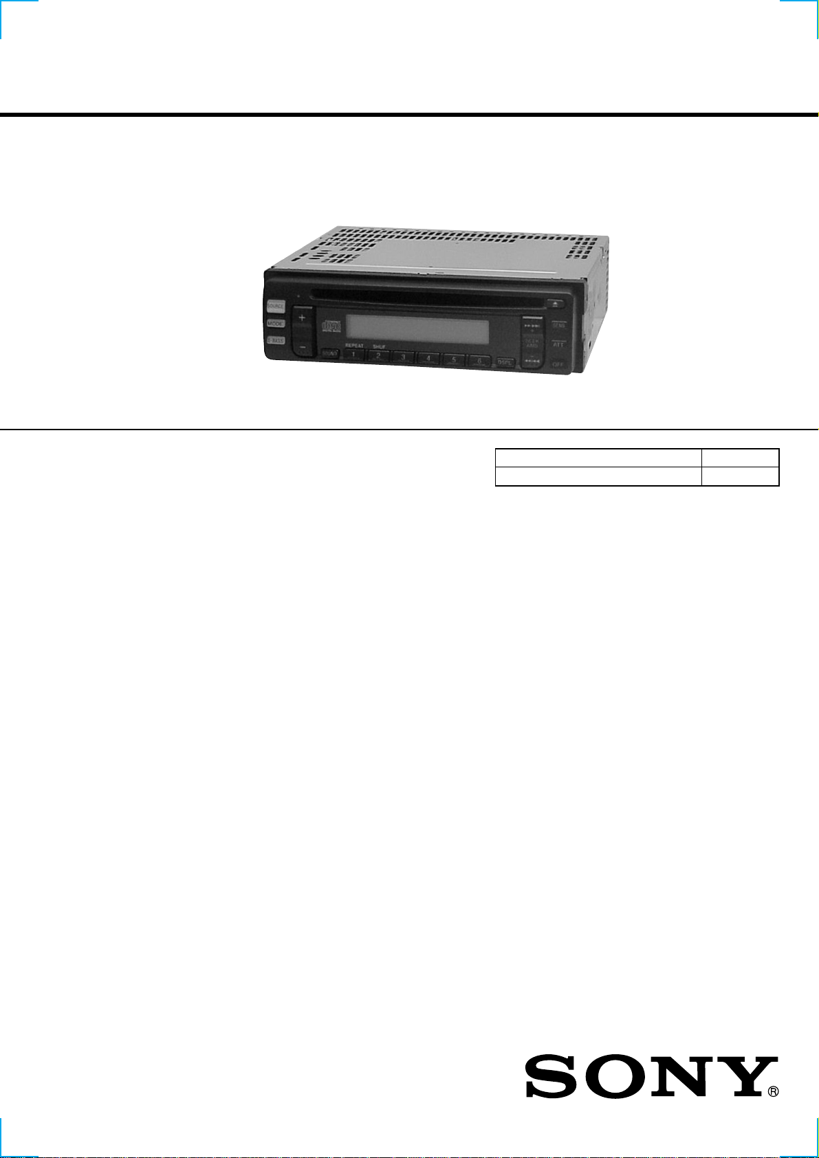
MDC-3600
SERVICE MANUAL
• The tuner and CD sections have no adjustments.
E Model
Model Name Using Similar Mechanism CDX-3600
CD Drive Mechanism Type MG-310-153
FM/AM COMPACT DISC PLAYER
1
Page 2

SERVICE NOTE
TABLE OF CONTENTS
CAUTION
Use of controls or adjustments or performance of procedures other than those specified herein may result in hazardous radiation exposure.
Notes on Chip Component Replacement
• Never reuse a disconnected chip component.
• Notice that the minus side of a tantalum capacitor may be dam-
aged by heat.
NOTES ON HANDLING THE OPTICAL PICK-UP BLOCK OR
BASE UNIT
The laser diode in the optical pick-up block may suffer electrostatic
breakdown because of the potential difference generated by the
charged electrostatic load, etc. on clothing and the human body.
During repair, pay attention to electrostatic breakdown and also use
the procedure in the printed matter which is included in the repair
parts.
The flexible board is easily damaged and should be handled with
care.
NOTES ON LASER DIODE EMISSION CHECK
The laser beam on this model is concentrated so as to be focused on
the disc reflective surface by the objective lens in the optical pick-up
block. Therefore, when checking the laser diode emission, observe
from more than 30 cm away from the objective lens.
Laser Diode Properties
• Material: GaAlAs
• Wavelength: 780 nm
• Emission Duration: continuous
• Laser Output Power: less than 44.6 µW*
* This output is the value measured at a distance of 200 mm from
the objective lens surfase on the Optical Pick-up Block.
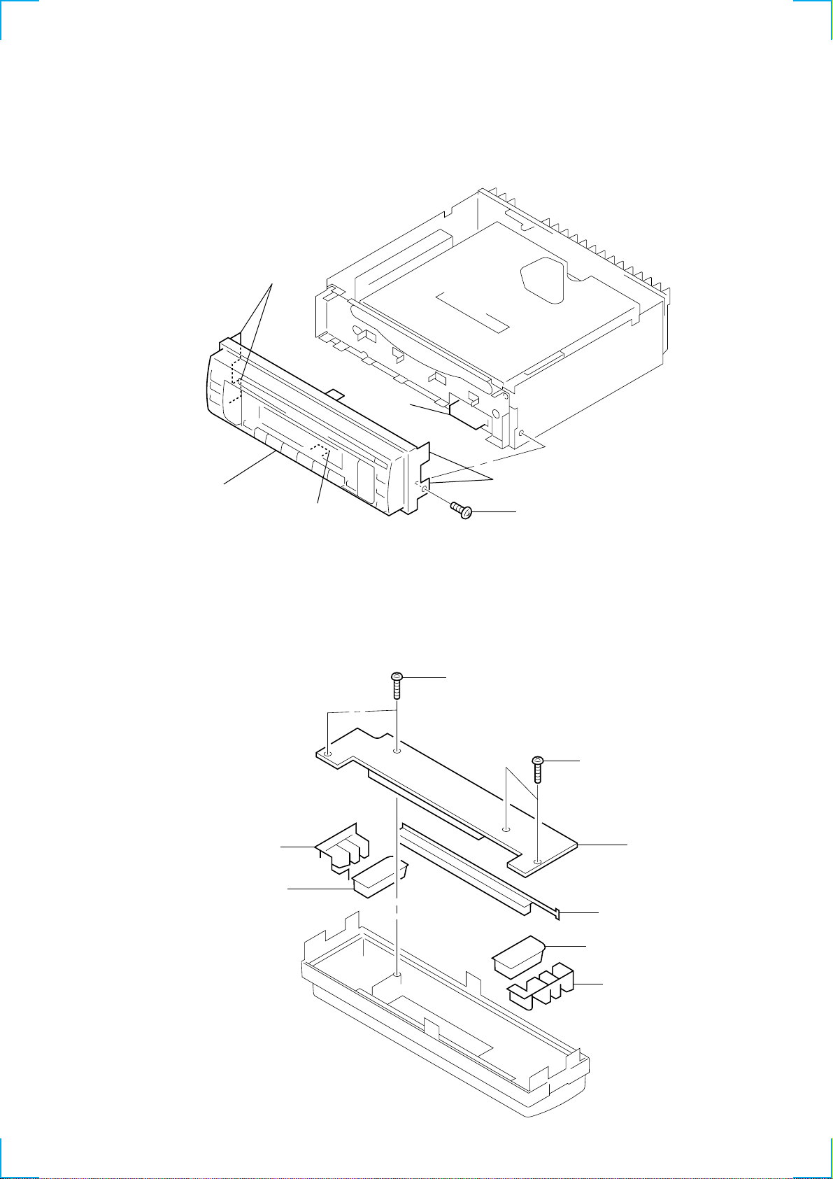
1. DISASSEMBLY
1-1. Front Panel Assy ................................................................. 3
1-2. Key Board ........................................................................... 3
1-3. Main Sub Assy .................................................................... 4
1-4. CD Mechanism Block .........................................................4
1-5. Heat Sink.............................................................................5
1-6. Chassis (R) Block Assy....................................................... 5
1-7. Floating Block Assy............................................................ 6
1-8. Roller Arm Assy.................................................................. 6
1-9. Optical Pick-up Block ......................................................... 7
2. DIAGRAMS
2-1. IC Pin Description............................................................... 8
2-2. Block Diagram –Main Section–........................................ 10
2-3. Block Diagram –Display Section–.................................... 11
2-4. Printed Wiring Boards –Main Section– ............................ 12
2-5. Schematic Diagram –Main Section (1/3)–........................ 14
2-6. Schematic Diagram –Main Section (2/3)–........................ 15
2-7. Schematic Diagram –Main Section (3/3)–........................ 16
2-8. Schematic Diagram –Display Section–.............................17
2-9. Printed Wiring Board –Display Section– .......................... 18
3. EXPLODED VIEWS
3-1. Chassis Section ................................................................. 21
3-2. Front Panel Section ........................................................... 22
3-3. CD Mechanism Section (1)............................................... 23
3-4. CD Mechanism Section (2)............................................... 24
4. ELECTRICAL PARTS LIST ........................................ 25
SAFETY-RELATED COMPONENT WARNING!!
COMPONENTS IDENTIFIED BY MARK 0 OR DOTTED LINE
WITH MARK 0 ON THE SCHEMATIC DIAGRAMS AND IN
THE PARTS LIST ARE CRITICAL TO SAFE OPERATION.
REPLACE THESE COMPONENTS WITH SONY PARTS WHOSE
P ART NUMBERS APPEAR AS SHOWN IN THIS MANU AL OR
IN SUPPLEMENTS PUBLISHED BY SONY.
2
Page 3
SECTION 1
DISASSEMBLY
Note : Follow the disassembly procedure in the numerical order given.
1-1. FRONT PANEL ASSY
3 claws
5 CN601
1-2. KEY BOARD
5 button (source)
6 front panel assy
4 claw
2 claws
1 PTT 2.6x8
1 P 2x8
2 P 2x8
3 KEY board
6 button (+.–)
4 button (6 key)
8 button (AMS)
7 button (EJECT)
3
Page 4
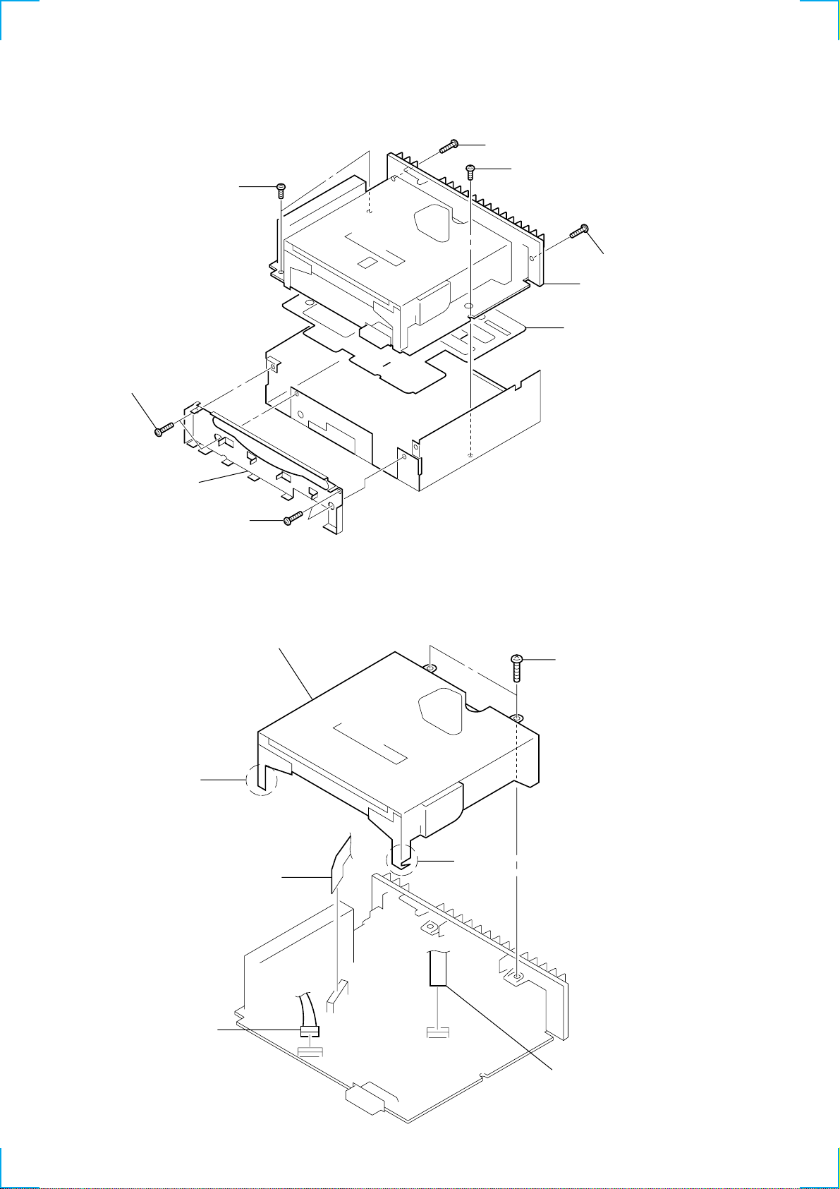
1-3. MAIN SUB ASSY
7 PTT 2.6x6
ground point
1 PTT 2.6x8
3 bracket (front)
4 PTT 2.6x8
6 PTT 2.6x6
ground point
5 PTT 2.6x8
8 main sub assy
9 sheet (insulating)
2 PTT 2.6x8
1-4. CD MECHANISM BLOCK
3 claw
7 CD mechanism block
1 PTT 2.6x8
2 claw
5 CNJ102
6 CN600
4 CNJ103
4
Page 5
1-5. HEAT SINK
4 heat sink
3 PTT 2.6x10
2 PTT 2.6x10
1-6. CHASSIS (R) BLOCK ASSY
1 PTT 2.6x10
3 tension spring (FL)
4 tension spring (FL)
2 chassis (R) block assy
1 screws (P 2x2.5)
5
Page 6
1-7. FLOATING BLOCK ASSY
4 tension spring (angle)
8
5
7
3 tension spring (SPM)
9 floating block assy
6
2 lever (LE.L)
1 washer (M)
1-8. ROLLER ARM ASSY
Note : When replacing the spring roller, replace the rollers at the right and left ends at the same time.
1 spring (roller)
6
5
7 roller arm assy
2 spring (roller)
4
3
6
Page 7
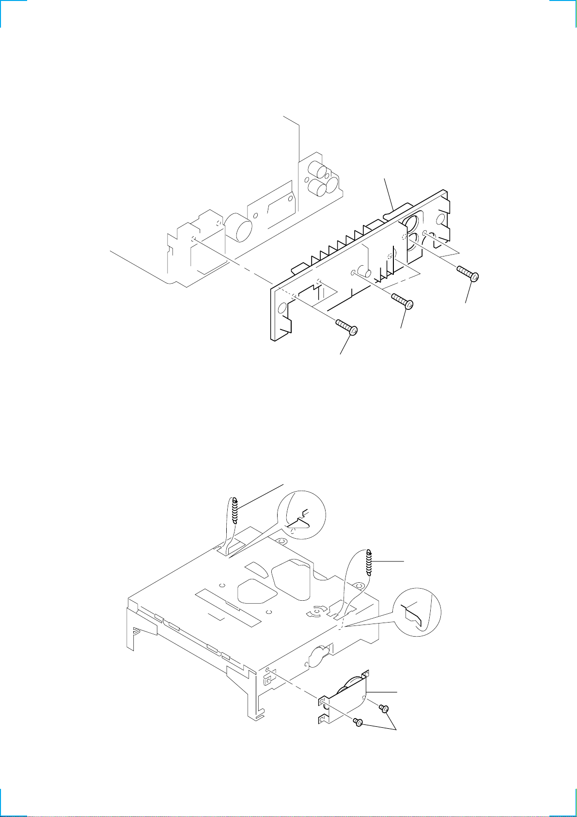
1-9. OPTICAL PICK-UP BLOCK
1 gear (worm wheel)
2 shaft (sled guide)
claw
3 optical pick-up block
7
Page 8
SECTION 2
DIAGRAMS
2-1. IC PIN DESCRIPTION
• IC600 µPD78005GC-156-8BT (SYSTEM CONTROL)
Pin No. Pin Name I/O Pin Description
1 MCLK O Microcomputer command clock signal output (data latch on rising)
2 MDATA O Microcomputer command data signal output
3 MLD O Microcomputer command load signal output
4 AVSS — Analog ground
5 DSTSEL0 I Destination select setting input (Connect to ground in this set.)
6 DSTSEL1 I 9k/10k select setting input (“L”: 9 kHz step, “H”: 10 kHz step)
7 AVREF1 I Analog reference voltage input
8 SUBQ I Sub code Q data input
9 ——Not used.
10 SQCK O Clock output for sub code Q register.
11 LCDCE O LCD driver serial chip enable output
12 LCDSO O LCD driver serial data output
13 LCDCKO O LCD driver serial clock output
14 ILLON O Illumination power control output
15 UNICKI I SONY-BUS serial interface clock input
16 UNISI I SONY-BUS serial interface data input
17 UNISO O SONY-BUS serial interface data output
18 UNICKO O SONY-BUS serial interface clock output
19 SBCK O Clock output for error correction result read-in.
20 BUSON O BUS ON control output
21 SYS RST O System reset control output
22 RST O DSP reset signal output (“L” active)
23 FOUT O Loading motor control output (Forward direction)
24 ROUT O Loading motor control output (Reverse direction)
25 CD-ON O CD power control output
26 PW-ON O System power control output
27 LIMSW I LIMIT switch input (“L” active)
28 FLAG I Data input for error correction result read-in.
29 SENS I SENS signal input
30 FLOCK I Focus servo pulling signal input (“L” active)
31 TLOCK I Tracking servo pulling signal input (“L” active)
32 STATE I Status signal input
33 VSS1 — Ground
34 VIB. I/O Vibration lens input/output
35 CDM-ON O CD machanism power control output
36 AMPMUT O Power amplifier mute control output
37 A-MUT O Audio mute control output
38 AD-ON O Power control output for A/D conversion.
39 PW-SEL O Not used in this set.
40 NOSESW I Front panel attachment detection input
41 TEST I Test mode direct setting input
42 TELMUT O Not used in this set.
43 ACCIN I Accessory power supply voltage detection input
44 VOLCE O Electric volume serial chip enable output
45 VOLSO O Electric volume serial data output
46 BEEP O Beep output
47 TUNON O Tuner ON output
48 FMON O FM ON output
49 PLLCE O PLL chip enable output
50 VOLCKO O Electric volume serial clock output
51 PLLSO O PLL data output
8
Page 9

Pin No. Pin Name I/O Pin Description
52 PLLCKO O PLL clock output
53 PLLSI I PLL data input
54 AMON O AM ON output
55 — — Not used in this set.
56 FMST I/O ST-IND indication input/Forced Monaural output
57 SW4 I Switch 4 input (“L” active)
58 SW3 I Switch 3 input (“L” active)
59 SW1 I Switch 1 input (“L” active)
60 RESET I System reset input
61 SIRCS I Remote commander input (Not used in this set)
62 KEYACK I Key input acknowledge
63 BUIN I Backup power supply detection input
64 BLKCK I Sub code block clock signal input (interruption)
65 SW2 I Switch 2 input (“L” active)
66 FCLK I Latch input for error correction result read-in. (interruption)
67 VSS0 — Ground
68 VDD1 — Power supply pin (+5 V)
69 X2 — Main system clock output (5 MHz)
70 X1 — Main system clock input (5 MHz)
71 VPP — Internal connection
72 XT2 — Sub system clock output (32.768 kHz)
73 XT1 — Sub system clock input (32.768 kHz)
74 VDD0 — Power supply pin (+5 V)
75 AVREF0 — Analog reference voltage input
76 KEYIN0 I Key input 0
77 KEYIN1 I Key input 1
78 S-METER I AM/FM S-meter voltage detection input
79 SD-IN I Signal detector input
80 LCDINH O LCD blank indication control output
99
Page 10

MDC-3600
2-2. BLOCK DIAGRAM — MAIN SECTION —
DIGITAL SIGNAL/
OPTICAL
PICK-UP
NB
NA
E
F
LPD
LD
M
M
M
J701
(ANTENNA)
DRIVE
Q101
VREF
15
16
17
18
12
11
14
13
10
BU5V
COM8V
CD8V
CD5V
9
MOTOR DRIVE
LD
F+
F-
T+
T-
M102
(SLED)
M101
(SPINDLE)
M103
(LOADING)
04
RF AMP
IC102
PDA ARF ARF
PDB
2
PDE
27 23
PDF
28
4
LPD
5
LD
26
VREF
IC103
FO
DRIVE
TR
DRIVE
SLED
MOTOR
DRIVE
SP
MOTOR
DRIVE
LOAD
MOTOR
DRIVE
NRFDET
26
23
6
3
28
1
5V REG
Q509,517
8V REG
Q511
5V REG
Q514,515
ENV
CROSS
VDET
BDO
OFTR
LDON
TBAL
FBAL
(LIMIT)
FE
TE
22
19
16
18
12
15
17
13
24
25
( )
BATT
BATT
PON+B
8V REG
Q512,513
SERVO PROCESSOR
44 731 9
32 75
FE
TE
33
RFENV
34
TRCRS
37 58
VDET
35
BDO
39 59
38
RF-DET
36
OFT
LDON
40
31
TBAL
30
FBAL
28
FOD
26
KICK
27
TRD
21
TRV
22
TVD
25
ECS
24
ECM
CHUCKING
DET
( )
DISC
IN2
BATT
IC101
L OUT
R OUT
X1
X2
RST
STAT
SUBQ
SQCK
BLKCK
TLOCK
FLOCK
SENSE
MLD
MDATA
MCLK
FLAG
FCLK
SBCK
SW2SW3SW4SW5
DISC
( )
IN1
X600
5.0MHz
X601
32.768kHz
36
IC600 (1/2)
AMP MUT
S-METER
37
38
A MUT
BEEP
PW ON
VOLPLL
CKO
TEST
ACC IN
BU IN
CKO
SD IN
FM ST
FM ON
AM ON
TU ON
CE
SO
CE
SO
R-CH
X101
16.93MHz
SYSTEM CONTROL
18
22
32
8
10
64
31
30
29
3
2
1
28
66
19
34
23
24
27
57
58
65
69
70
72
73
35
25
RST
STATE
SUBQ
SQCK
BLKCK
TLOCK
FLOCK
SENS
MLD
MDATA
MCLK
FLAG
FCLK
SBCK
VIB
FOUT
ROUT
LIMSW
SW4
SW3
SW2
X2
X1
XT2
XT1
CDM ON
CDON
17
15
14
13
12
11
10
9
8
7
65
63
56
37
46
36
26
44
45
50
41
43
63
49
51
52
53
SI
78
79
56
48
54
47
ELECTRIC VOLUME
ACC/BATT
CHECK
Q507
BATT
CHECK
Q510
X700
10.25MHz
COM8V
IC400
VOL/
TONE
CEDICLK
18 17 16
FADER
BATT
BATT
CE
3
DIN
4
5
CLK
DOUT
6
1
XTOUT
XTIN
24
POWER
CONTROL
Q704,705
PLL
IC700
OSC OUT
LR
LF
LO/DX
AM CP
VT
FM CP
FM IN
FM IN
IFC R
IFC IN
TU8V
POWER
CONTROL
Q701
20
21
Q402
(1/2)
10
20
19
18
16
15
2
11
13
BATT
MUTE
CONTROL
Q550,551
R-CH
R-CH
POWER
CONTROL
Q702
POWER
CONTROL
Q501,502(1/2)
12
17
15
4
5
6
13
20
18
19
21
9
10
8
BU5V
Q401
(1/2)
Q402
(2/2)
SHUTDOWN
MUTE
Q516
TUNER UNIT
TU700
AMDET
L OUT
R OUT
LO/DX
VT (FM/AM)
VCO (FM/AM)
XTAL IN
IFC-O/SEEK/RE
S-METER
SD (AM/FM)
MONO/ST
+B (FM/AM)
AM+B
FM+B
POWER
CONTROL
Q703
P ON+B
AM
FM
R-CH
BATT
TU5V
POWER
CONTROL
Q502(2/2),505
1
2
POWER AMP
IC500
11
12
MUTE
22 4
• Signal path
: FM
: AM
: CD
STBY
-2
R-CH
-1
CNP500
9
7
5
3
R-CH
BATT
F901
PON+B
2
REAR L(+)
10
REAR L(–)
1
FRONT L(+)
FRONT L(–)
9
3
REAR R(+)
11
REAR R(–)
FRONT R(+)
4
FRONT R(–)
12
16
BATT
6
ANT REM
5
AMP REM
TEST
15
7
ACC
R
L
CNP400
AUDIO OUT
REAR
10 10
Page 11

MDC-3600
2-3. BLOCK DIAGRAM — DISPLAY SECTION —
BATT
SYSTEM CONTROL
IC600 (2/2)
ILL ON
RESET
CKO
SO
LCD
CE
INH
KEYIN0
KEYIN1
AVREFO
KEYACK
AD ON
DSTSEL1
04
10V REG
Q503,504
14
60
LSW800
(RESET)
13
12
11
80
76
77
75
62
38
6
LSW801-819
57 60 62 61
DI
CE
INH
LIQUID CRYSTAL
DISPLAY PANEL
LCD800
LSW801-819
KEY
ACTIVE
Q601
FM200k
AM10k
( )
FM50k
AM9k
LCD DRIVE
CLK
S602
FREQUENCY
SELECT
IC800
BU5V
PL801
( )
PL802
IC601
1 2
RESET
5V
REG
D851
LCD
BACK
LIGHT
VDD
BU5V
THIS NOTE IS COMMON FOR PRINTED WIRING BOARDS
AND SCHEMATIC DIAGRAMS.
(In addition to this, the necessary note is
printed in each block.)
For schematic diagrams
• All capacitors are in µF unless otherwise noted. pF: µµF
50 WV or less are not indicated except for electrolytics
and tantalums.
• All resistors are in Ω and 1/
specified.
4
W or less unless otherwise
• % : indicates tolerance.
f
•
: internal component.
• C : panel designation.
Note: The components identified by mark 0 or dotted line
with mark 0 are critical for safety.
Replace only with part number specified.
• U : B+ Line.
• Power voltage is dc 14.4V and fed with regulated dc power
supply from ACC and BATT cords.
• Voltages are taken with a VOM (Input impedance 10 MΩ).
Voltage variations may be noted due to normal production tolerances.
• Waveforms are taken with a oscilloscope.
Voltage variations may be noted due to normal production tolerances.
• Circled numbers refer to waveforms.
• Signal path.
F : FM
f : AM
J : CD
For printed wiring boards
• X : parts extracted from the component side.
• Y : parts extracted from the conductor side.
a
•
•
: Through hole.
f
: internal component.
• b : Pattern from the side which enables seeing.
(The other layer’s patterns are not indicated.)
Caution:
Pattern face side: Parts on the pattern face side seen from the
(Side B) pattern face are indicated.
Parts face side: Parts on the parts face side seen from the
(Side A) parts face are indicated.
11 11
Page 12

MDC-3600
• Semiconductor
Location
Ref. No. Location
(D501) C-11
D502 F-11
D503 B-13
D504 C-12
D505 B-11
D506 D-13
D507 D-13
D508 E-11
D509 F-11
D510 E-12
D511 B-4
D512 E-10
D513 B-8
D514 D-8
D516 C-12
D517 C-12
D518 C-13
D519 C-2
D520 D-9
D521 D-9
D522 D-9
D523 D-9
D524 C-9
D525 C-9
D526 C-9
D527 C-9
D528 B-11
D529 B-12
D550 C-4
D551 B-4
D602 J-12
2-4. PRINTED WIRING BOARDS — MAIN SECTION —
IC101 G-7
IC102 H-5
IC103 J-4
IC400 D-5
(IC500) B-6
IC600 H-11
IC601 I-9
IC700 D-3
Q101 F-4
Q401 B-3
Q402 C-5
Q403 C-6
Q501 D-10
Q502 D-12
Q503 F-13
Q504 G-12
Q505 D-11
Q507 D-12
Q509 E-11
Q510 E-12
Q511 E-10
Q512 C-8
(Q513) B-8
Q514 C-8
Q515 D-7
Q516 B-3
Q517 F-11
Q550 B-3
Q551 B-4
Q601 J-13
Q701 G-2
Q702 G-2
Q703 J-7
Q704 F-2
Q705 F-2
( ) : SIDE B
SW3
(DISC IN 2)
SW2
(DISC IN 1)
+
–
67
SW4
CHUCKING
( )
DET
1
2
3
4
12 12
Page 13

MDC-3600
BLK
YEL
BLU
RED
BLU/WHT
+
-
VIO
GRY
GRY/BLK
+-+-+-+
AMP REM
FRONT R-CH
GRN
VIO/BLK
REAR R-CH
(LIMIT)
(LIMIT)
WHT
GRN/BLK
REAR L-CH
WHT/BLK
-
FRONT L-CH
+
( )
-
(Page 18)
13 13
Page 14

MDC-3600
2-5. SCHEMATIC DIAGRAM — MAIN SECTION (1/3) — • Refer to page 19 for IC Block Diagrams.
• Waveforms (MODE:PLAY)
1
1.3Vp-p
(Page 15)
2
3
4
5
6
IC102
Approx. 200mVp-p
IC102
Approx. 600mVp-p
IC102
IC101
td
IC101
(ARF)
9
(TE)
ws
(FE)
wd
1.95µsec
(PCK/DSLB)
16.93MHz
(X2)
tl
0V
0V
5Vp-p
4Vp-p
(Page 16)
4.2Vp-p
5MHz
yl
(X2)
IC600
7
3Vp-p
32.768kHz
ud
(XT1)
IC600
Note:
• Voltage is dc with respect to ground under no-signal
condition.
no mark : CD PLAY
14 14
Page 15

2-6. SCHEMATIC DIAGRAM — MAIN SECTION (2/3) — • Refer to page 20 for IC Block Diagrams.
TDA7386
U1GC44-TE12R
U1GC44-TE12R
U1GC44-TE12R
U1GC44-TE12R
U1GC44-TE12R
U1GC44-TE12R
U1GC44-TE12R
U1GC44-TE12R
MDC-3600
(Page 14)
(Page 16)
Note:
• Voltage is dc with respect to ground under no-signal
(detuned) condition.
no mark : FM
15 15
Page 16

MDC-3600
2-7. SCHEMATIC DIAGRAM — MAIN SECTION (3/3) — • Refer to page 20 for IC Block Diagrams. Refer to page 14 for Waveforms.
(Page 14)
(Page 15)
16 16
(Page 17)
Note:
• Voltage is dc with respect to ground under no-signal
(detuned) condition.
no mark : FM
(): AM
< > : CD PLAY
Page 17

2-8. SCHEMATIC DIAGRAM — DISPLAY SECTION —
(Page 16)
MDC-3600
17 17
Note:
• Voltage is dc with respect to ground under no-signal
(detuned) condition.
no mark : FM
Page 18

MDC-3600
2-9. PRINTED WIRING BOARD — DISPLAY SECTION —
(Page 13)
18 18
Page 19

• IC Block Diagrams
IC102 AN8835SB-E1
PDA
PDB
VCC
LPD
RFO
RFI
CAGC
ARF
CSBRT
CEA
BDO
LD ON
GND
RX
1
2
3
4
LD
5
6
7
8
9
10
11
12
13
14
A
B
RF EQ
AGC
OFFR DET
3 TENV
A CH
VCBA
B CH
RF DET
BDO DET
RX
F CH
VCBA
E CH
F
E
28
27
26
25
24
23
22
21
20
19
18
17
16
15
PDF
PDE
REF
V
F BAL
T BAL
FE
TE
CCRS
TE BPF
ENV
V DET
OFFR
CROSS
NRF DET
IC103 BA5984FP-E2
REV
OPIN4(+)
2728 26 25
LOADING DRIVER
REV
FWD
FWD
OPIN4(–)
+–
OUT B
OUT A
+–+–
PIN1(+)
PIN1(–)
OPOUT4
OPIN3(+)
OPIN3(–)
PIN2(–)
OPOUT3
–
+
+
–
OPOUT2
24 23 22 21 20 19 18 17 16 15
+–
–
+
+
–
4 5 6 7 8 9 10 11 12 13 1421 3
PIN2(+)
OPOUT1
MUTE
VCC
MUTE
VCC
BIAS
VOL(–)
GND
VOL(+)
VO3(–)
+–
+–
–+
LEVEL
SHIFT
LEVEL
SHIFT
–+
+–
+–
VO2(–)
VO3(+)
VO2(+)
VO4(–)
+–
+–
–+
LEVEL
SHIFT
LEVEL
SHIFT
–+
+–
+–
VO1(–)
VO4(+)
VO1(+)
19
Page 20

IC400 LC75374E
34
LSELO
35
L4
L3
36
L2
37
L1
38
39
VDD
R1
40
41
R2
R3
42
R4
43
44
RSELO
LVRIN
1
RVRIN
LT3
LT2
+
–
–
+
LT1
–
+
+
–
+
–
DECODER LATCH
+
–
RT1
RT2
RT3
LCOM
+
–
+
–
–
+
–
+
2 345 6 7 8 9
RCOM
LSIN
LTOUT
CONTROL
REGISTER
RSIN
RTOUT
NC
2627282930313233
SHIFT
NC
LSB2
LSB1
NC
2324
25
22
LFIN
+
–
+
+
–
10
11
NC
RSB1
RSB2
–
+
–
–
+
–
+
LFOUT
21
LROUT
20
19
VREF
18
CE
17
DI
16
CL
15
VSS
14
RROUT
RFOUT
13
12
RFIN
IC700 TB2118F (EL)
XO
1
OSC
2
BUFF
CE
3
D IN
4
CK
5
D OUT
6
7
SR
8
I/O 1
9
I/O 2
10
OUT1
11
OUT2
12
VDD2
OSCILLATOR
ON/OFF
SERIAL
INTERFACE
18 BIT
18 BIT
I/O PORT
OUTPUT PORT
REFERENCE
DIVIDER
22 BIT
40BIT SHIFT
REGISTER
20 BIT
IF COUNTER
REF
PHASE
COMPARATOR
SIG
12 BIT
PROGRAMMABLE
COUNTER
4 BIT
SWALLOW
COUNTER
REGULATED
POWER SUPPLY
SELECT
SELECT
PRESCALER
24
XI
23
A GND
+
–
+
–
AMP
AMP
AMP
22
REG
21
VCC
20
AM CP
19
VT
18
FM CP
17
D GND
16
AM IN
15
FM IN
14
VDD
13
IFC
20
Page 21

NOTE:
• The mechanical parts with no reference
number in the exploded views are not supplied.
• Items marked “*” are not stocked since
they are seldom required for routine service.
Some delay should be anticipated
when ordering these items.
• -XX and -X mean standardized parts, so
they may have some difference from the
original one.
3-1. CHASSIS SECTION
SECTION 3
EXPLODED VIEWS
• Color Indication of Appearance Parts
Example :
KNOB, BALANCE (WHITE) ... (RED)
R
Parts Color Cabinet’s Color
• Hardware (# mark) list are given in
the last of this parts list.
The components identified by
mark 0 or dotted line with mark
R
0 are critical for safety.
Replace only with part number
specified.
TU700
MG-310-153
10
2
3
#1
1
5
#1
9
#5
#5
#5
#1
4
F901
6
#1
Ref. No. Part No. Description Remark
* 1 3-034-437-02 COVER
2 3-376-464-11 SCREW (+PTT 2.6X6), GROUND POINT
* 3 A-3283-023-A MAIN BOARD, COMPLETE
* 4 3-043-234-01 BRACKET (IC)
5 1-776-207-61 CORD (WITH CONNECTOR) (POWER)
* 6 3-043-233-02 HEAT SINK
7
#1
#1
Ref. No. Part No. Description Remark
* 7 3-034-439-02 BRACKET (FRONT)
* 8 3-034-436-03 CHASSIS
* 9 3-034-455-03 SHEET (INSULATING)
10 3-360-123-01 PLATE (C), GROUND
F901 1-532-877-11 FUSE (BLADE TYPE) (AUTO FUSE) 10A
TU700 A-3220-689-A TUNER UNIT (TUX-010/2(E))
8
21
Page 22

3-2. FRONT PANEL SECTION
57
53
51
54
#2
55
#2
LCD800
52
58
59
60
56
61
Ref. No. Part No. Description Remark Ref. No. Part No. Description Remark
* 51 A-3283-015-A KEY BOARD, COMPLETE
* 52 3-034-440-02 PLATE (LCD), GROUND
* 53 3-034-454-01 SHEET (LCD)
* 54 3-034-453-21 SHEET (DIFFUSION)
* 55 X-3377-104-1 HOLDER (LCD) ASSY
57 3-045-627-01 BUTTON (SOURCE)
58 3-034-450-04 BUTTON (+.–)
59 3-034-443-02 BUTTON (6 KEY)
60 3-034-451-04 BUTTON (AMS)
61 X-3379-325-1 PANEL ASSY, FRONT
* 56 3-034-445-21 BUTTON (EJECT)
22
LCD800 1-804-156-11 DISPLAY PANEL, LIQUID CRYSTAL
Page 23

3-3. CD MECHANISM SECTION (1)
B
111
112
114
113
102
103
103
103
104
104
104
107
108
106
109
109
110
105
114
101
115
116
B
A
C
C
A
#3
M103
#4
not supplied
(MG-310-153)
Ref. No. Part No. Description Remark Ref. No. Part No. Description Remark
101 X-3378-793-1 ARM ASSY, ROLLER
* 102 3-032-327-02 LEVER (LE.L)
103 3-037-492-01 DAMPER (P)
104 3-033-808-01 SCREW (M2X4.0)
105 3-042-644-01 SPRING (LEVER DLR)
106 3-032-373-01 SPRING (SPM), TENSION
107 3-033-806-01 SCREW (M2X2.5)
108 3-042-642-01 SPRING (LEVER D)
109 3-032-351-01 SPRING (FL), TENSION
110 3-032-352-01 SPRING (ANGLE), TENSION
111 X-3378-335-5 CHASSIS (M) COMPLETE ASSY
* 112 1-670-827-11 SW BOARD
113 3-033-807-01 SCREW (M2X3.0)
114 3-032-359-01 SPRING (ROLLER)
115 3-039-600-02 ROLLER (SS)
116 3-933-152-02 ROLLER (S)
M103 X-3378-888-1 MOTOR ASSY, LOADING (LOADING)
23
Page 24

3-4. CD MECHANISM SECTION (2)
(MG-310-153)
152
173
151
172
M101
171
163
not supplied
153
170
157
158
169
M102
155
159
154
156
not supplied
160
161
162
not supplied
168
164
165
Ref. No. Part No. Description Remark Ref. No. Part No. Description Remark
151 A-3301-693-A ARM ASSY, CHUCKING
152 3-033-805-01 SCREW (M2X2.0)
* 153 3-027-473-01 CUSHION (EJ2)
154 3-032-353-01 SPRING (CH), TENSION
155 3-033-803-01 SCREW (M1.7X2.5)
* 156 X-3376-720-4 CHASSIS (OP) ASSY
157 3-032-373-01 SPRING (SPM), TENSION
* 158 X-3376-724-1 LEVER (WORM WHEEL) ASSY
159 3-042-642-01 SPRING (LEVER D)
* 160 1-670-828-11 MOTOR BOARD
161 3-033-807-01 SCREW (M2X3.0)
162 3-032-341-01 BRACKET (SL MOTOR)
0 163 X-3378-023-1 PICK-UP ASSY, OPTICAL
164 3-032-345-02 RACK (FEED)
165 3-033-804-01 SCREW (+PTP 1.7X4)
166 3-032-358-02 SHAFT (SLED GUIDE)
167 3-032-344-01 GEAR (WORM WHEEL)
168 1-673-761-11 MOTOR FLEXIBLE BOARD
169 3-366-892-01 SCREW (M1.4X1.1)
* 170 3-037-490-01 CUSHION (DH)
171 3-042-739-01 COVER (P)
* 172 3-027-767-01 RETAINER (DISC)
173 3-931-894-01 BRACKET (CP)
M101 X-3379-269-1 MOTOR ASSY, SPINDLE (SPINDLE)
M102 X-3377-704-1 MOTOR ASSY, SLED (SLED)
167
166
The components identified by
mark 0 or dotted line with mark
0 are critical for safety.
Replace only with part number
specified.
24
Page 25

SECTION 4
ELECTRICAL PARTS LIST
NOTE:
• Due to standardization, replacements in
the parts list may be different from the
parts specified in the diagrams or the
components used on the set.
• -XX and -X mean standardized parts, so
they may have some difference from the
original one.
• RESISTORS
All resistors are in ohms.
METAL:Metal-film resistor.
METAL OXIDE: Metal oxide-film resistor.
F:nonflammable
Ref. No. Part No. Description Remark Ref. No. Part No. Description Remark
* A-3283-015-A KEY BOARD, COMPLETE
********************
* 3-034-440-02 PLATE (LCD), GROUND
* 3-034-453-21 SHEET (DIFFUSION)
* 3-034-454-01 SHEET (LCD)
< CAPACITOR >
• Items marked “*” are not stocked since
they are seldom required for routine service.
Some delay should be anticipated
when ordering these items.
• SEMICONDUCTORS
In each case, u : µ, for example:
uA.. : µA.. uPA.. : µPA..
uPB.. : µPB.. uPC.. : µPC.. uPD.. : µPD..
• CAPACITORS
uF : µF
• COILS
uH : µH
LSW817 1-762-619-21 SWITCH, KEY BOARD (WITH LED) (4)
LSW818 1-762-619-21 SWITCH, KEY BOARD (WITH LED) (5)
LSW819 1-762-619-21 SWITCH, KEY BOARD (WITH LED) (6)
PL801 1-517-898-21 LAMP, PILOT
PL802 1-517-898-21 LAMP, PILOT
The components identified by
mark 0 or dotted line with mark
0 are critical for safety.
Replace only with part number
specified.
When indicating parts by reference
number, please include the board.
< PILOT LAMP >
KEY
C851 1-107-826-11 CERAMIC CHIP 0.1uF 10% 16V
C853 1-162-970-11 CERAMIC CHIP 0.01uF 10% 25V
C854 1-115-412-11 CERAMIC CHIP 680PF 5% 25V
< CONNECTOR >
CN800 1-785-773-21 PIN, CONNECTOR 15P
< DIODE >
D851 8-719-976-99 DIODE HZU4.7B2TRF
< IC >
IC800 8-759-330-60 IC LC75822WD
< LIQUID CRYSTAL DISPLAY >
LCD800 1-804-156-11 DISPLAY PANEL, LIQUID CRYSTAL
< SWITCH >
LSW800 1-771-206-11 SWITCH, KEY BOARD (WITH LED) (RESET)
LSW801 1-762-619-21 SWITCH, KEY BOARD (WITH LED) (OFF)
LSW802 1-762-619-21 SWITCH, KEY BOARD (WITH LED) (SOURCE)
LSW803 1-762-619-21 SWITCH, KEY BOARD (WITH LED) (MODE)
LSW804 1-762-619-21 SWITCH, KEY BOARD (WITH LED) (SOUND)
LSW805 1-762-619-21 SWITCH, KEY BOARD (WITH LED) (+)
LSW806 1-762-619-21 SWITCH, KEY BOARD (WITH LED) (–)
LSW807 1-762-619-21 SWITCH, KEY BOARD (WITH LED) (SEEK/AMS
M > +)
LSW808 1-762-619-21 SWITCH, KEY BOARD (WITH LED) (SEEK/AMS
– m .)
LSW809 1-762-619-21 SWITCH, KEY BOARD (WITH LED) (SENS)
< RESISTOR >
R801 1-216-821-11 METAL CHIP 1K 5% 1/16W
R802 1-216-823-11 METAL CHIP 1.5K 5% 1/16W
R803 1-216-825-11 METAL CHIP 2.2K 5% 1/16W
R804 1-216-827-11 METAL CHIP 3.3K 5% 1/16W
R805 1-216-829-11 METAL CHIP 4.7K 5% 1/16W
R806 1-216-831-11 METAL CHIP 6.8K 5% 1/16W
R807 1-216-835-11 METAL CHIP 15K 5% 1/16W
R808 1-216-839-11 METAL CHIP 33K 5% 1/16W
R809 1-216-845-11 METAL CHIP 100K 5% 1/16W
R811 1-216-821-11 METAL CHIP 1K 5% 1/16W
R812 1-216-823-11 METAL CHIP 1.5K 5% 1/16W
R813 1-216-825-11 METAL CHIP 2.2K 5% 1/16W
R814 1-216-827-11 METAL CHIP 3.3K 5% 1/16W
R815 1-216-829-11 METAL CHIP 4.7K 5% 1/16W
R816 1-216-831-11 METAL CHIP 6.8K 5% 1/16W
R817 1-216-835-11 METAL CHIP 15K 5% 1/16W
R818 1-216-839-11 METAL CHIP 33K 5% 1/16W
R830 1-216-619-11 METAL CHIP 47 0.5% 1/10W
R831 1-216-619-11 METAL CHIP 47 0.5% 1/10W
R832 1-216-619-11 METAL CHIP 47 0.5% 1/10W
R833 1-216-619-11 METAL CHIP 47 0.5% 1/10W
R834 1-216-619-11 METAL CHIP 47 0.5% 1/10W
R835 1-216-627-11 METAL CHIP 100 0.5% 1/10W
R851 1-216-045-00 METAL CHIP 680 5% 1/10W
R852 1-216-821-11 METAL CHIP 1K 5% 1/16W
R853 1-218-733-11 METAL CHIP 51K 0.5% 1/16W
*************************************************************
LSW810 1-762-619-21 SWITCH, KEY BOARD (WITH LED) (ATT)
LSW811 1-762-619-21 SWITCH, KEY BOARD (WITH LED) (Z)
LSW812 1-762-619-21 SWITCH, KEY BOARD (WITH LED) (D-BASS)
LSW813 1-762-619-21 SWITCH, KEY BOARD (WITH LED) (DSPL)
LSW814 1-762-619-21 SWITCH, KEY BOARD (WITH LED) (1/REPEAT)
LSW815 1-762-619-21 SWITCH, KEY BOARD (WITH LED) (2/SHUF)
LSW816 1-762-619-21 SWITCH, KEY BOARD (WITH LED) (3)
25
Page 26

MAIN
Ref. No. Part No. Description Remark Ref. No. Part No. Description Remark
* A-3283-023-A MAIN BOARD, COMPLETE
*********************
* 3-043-233-02 HEAT SINK
* 3-043-234-01 BRACKET (IC)
7-685-794-09 SCREW +PTT 2.6X10 (S)
< CAPACITOR >
C101 1-117-681-11 ELECT CHIP 100uF 20% 16V
C102 1-109-982-11 CERAMIC CHIP 1uF 10% 10V
C103 1-162-970-11 CERAMIC CHIP 0.01uF 10% 25V
C104 1-124-779-00 ELECT CHIP 10uF 20% 16V
C105 1-107-826-11 CERAMIC CHIP 0.1uF 10% 16V
C106 1-107-826-11 CERAMIC CHIP 0.1uF 10% 16V
C108 1-162-964-11 CERAMIC CHIP 0.001uF 10% 50V
C110 1-162-968-11 CERAMIC CHIP 0.0047uF 10% 50V
C111 1-162-968-11 CERAMIC CHIP 0.0047uF 10% 50V
C112 1-115-412-11 CERAMIC CHIP 680PF 5% 25V
C113 1-107-826-11 CERAMIC CHIP 0.1uF 10% 16V
C114 1-164-227-11 CERAMIC CHIP 0.022uF 10% 25V
C115 1-109-982-11 CERAMIC CHIP 1uF 10% 10V
C116 1-117-681-11 ELECT CHIP 100uF 20% 16V
C117 1-109-982-11 CERAMIC CHIP 1uF 10% 10V
C118 1-162-970-11 CERAMIC CHIP 0.01uF 10% 25V
C119 1-115-565-11 CERAMIC CHIP 2.2uF 10% 10V
C120 1-162-959-11 CERAMIC CHIP 330PF 5% 50V
C121 1-164-315-11 CERAMIC CHIP 470PF 5% 50V
C122 1-164-227-11 CERAMIC CHIP 0.022uF 10% 25V
C123 1-165-176-11 CERAMIC CHIP 0.047uF 10% 16V
C124 1-162-968-11 CERAMIC CHIP 0.0047uF 10% 50V
C125 1-107-826-11 CERAMIC CHIP 0.1uF 10% 16V
C126 1-107-826-11 CERAMIC CHIP 0.1uF 10% 16V
C127 1-165-176-11 CERAMIC CHIP 0.047uF 10% 16V
C128 1-107-826-11 CERAMIC CHIP 0.1uF 10% 16V
C129 1-107-826-11 CERAMIC CHIP 0.1uF 10% 16V
C130 1-107-826-11 CERAMIC CHIP 0.1uF 10% 16V
C131 1-162-979-11 CERAMIC CHIP 0.0027uF 10% 50V
C132 1-164-227-11 CERAMIC CHIP 0.022uF 10% 25V
C133 1-117-681-11 ELECT CHIP 100uF 20% 16V
C134 1-107-826-11 CERAMIC CHIP 0.1uF 10% 16V
C135 1-117-681-11 ELECT CHIP 100uF 20% 16V
C136 1-117-681-11 ELECT CHIP 100uF 20% 16V
C138 1-117-681-11 ELECT CHIP 100uF 20% 16V
C139 1-107-826-11 CERAMIC CHIP 0.1uF 10% 16V
C140 1-107-826-11 CERAMIC CHIP 0.1uF 10% 16V
C141 1-109-982-11 CERAMIC CHIP 1uF 10% 10V
C147 1-110-501-11 CERAMIC CHIP 0.33uF 10% 16V
C148 1-107-826-11 CERAMIC CHIP 0.1uF 10% 16V
C149 1-162-964-11 CERAMIC CHIP 0.001uF 10% 50V
C154 1-107-826-11 CERAMIC CHIP 0.1uF 10% 16V
C401 1-164-489-11 CERAMIC CHIP 0.22uF 10% 16V
C402 1-107-826-11 CERAMIC CHIP 0.1uF 10% 16V
C403 1-109-982-11 CERAMIC CHIP 1uF 10% 10V
C404 1-109-982-11 CERAMIC CHIP 1uF 10% 10V
C405 1-109-982-11 CERAMIC CHIP 1uF 10% 10V
C406 1-162-967-11 CERAMIC CHIP 0.0033uF 10% 50V
C407 1-164-227-11 CERAMIC CHIP 0.022uF 10% 25V
C408 1-109-982-11 CERAMIC CHIP 1uF 10% 10V
C409 1-107-826-11 CERAMIC CHIP 0.1uF 10% 16V
C410 1-107-826-11 CERAMIC CHIP 0.1uF 10% 16V
C411 1-109-982-11 CERAMIC CHIP 1uF 10% 10V
C412 1-124-779-00 ELECT CHIP 10uF 20% 16V
C413 1-162-970-11 CERAMIC CHIP 0.01uF 10% 25V
C414 1-162-970-11 CERAMIC CHIP 0.01uF 10% 25V
C415 1-117-681-11 ELECT CHIP 100uF 20% 16V
C420 1-124-779-00 ELECT CHIP 10uF 20% 16V
C422 1-107-823-11 CERAMIC CHIP 0.47uF 10% 16V
C424 1-164-230-11 CERAMIC CHIP 220PF 5% 50V
C425 1-162-927-11 CERAMIC CHIP 100PF 5% 50V
C430 1-124-779-00 ELECT CHIP 10uF 20% 16V
C432 1-107-823-11 CERAMIC CHIP 0.47uF 10% 16V
C452 1-107-826-11 CERAMIC CHIP 0.1uF 10% 16V
C453 1-109-982-11 CERAMIC CHIP 1uF 10% 10V
C454 1-109-982-11 CERAMIC CHIP 1uF 10% 10V
C455 1-109-982-11 CERAMIC CHIP 1uF 10% 10V
C456 1-162-967-11 CERAMIC CHIP 0.0033uF 10% 50V
C457 1-164-227-11 CERAMIC CHIP 0.022uF 10% 25V
C458 1-109-982-11 CERAMIC CHIP 1uF 10% 10V
C459 1-107-826-11 CERAMIC CHIP 0.1uF 10% 16V
C460 1-107-826-11 CERAMIC CHIP 0.1uF 10% 16V
C461 1-109-982-11 CERAMIC CHIP 1uF 10% 10V
C464 1-164-230-11 CERAMIC CHIP 220PF 5% 50V
C465 1-162-927-11 CERAMIC CHIP 100PF 5% 50V
C470 1-124-779-00 ELECT CHIP 10uF 20% 16V
C472 1-107-823-11 CERAMIC CHIP 0.47uF 10% 16V
C480 1-124-779-00 ELECT CHIP 10uF 20% 16V
C482 1-107-823-11 CERAMIC CHIP 0.47uF 10% 16V
C500 1-107-826-11 CERAMIC CHIP 0.1uF 10% 16V
C501 1-126-768-11 ELECT 2200uF 20% 16V
C502 1-115-339-11 CERAMIC CHIP 0.1uF 10% 50V
C506 1-126-204-11 ELECT CHIP 47uF 20% 16V
C509 1-162-970-11 CERAMIC CHIP 0.01uF 10% 25V
C510 1-107-826-11 CERAMIC CHIP 0.1uF 10% 16V
C511 1-109-982-11 CERAMIC CHIP 1uF 10% 10V
C513 1-162-970-11 CERAMIC CHIP 0.01uF 10% 25V
C516 1-109-982-11 CERAMIC CHIP 1uF 10% 10V
C518 1-107-823-11 CERAMIC CHIP 0.47uF 10% 16V
C519 1-162-915-11 CERAMIC CHIP 10PF 0.5PF 50V
C520 1-107-826-11 CERAMIC CHIP 0.1uF 10% 16V
C522 1-107-826-11 CERAMIC CHIP 0.1uF 10% 16V
C524 1-117-681-11 ELECT CHIP 100uF 20% 16V
C532 1-107-823-11 CERAMIC CHIP 0.47uF 10% 16V
C533 1-124-779-00 ELECT CHIP 10uF 20% 16V
C534 1-126-926-11 ELECT 1000uF 20% 10V
C535 1-115-467-11 CERAMIC CHIP 0.22uF 10% 10V
C550 1-165-112-11 CERAMIC CHIP 0.33uF 16V
C551 1-117-681-11 ELECT CHIP 100uF 20% 16V
26
Page 27

MAIN
Ref. No. Part No. Description Remark Ref. No. Part No. Description Remark
C602 1-107-826-11 CERAMIC CHIP 0.1uF 10% 16V
C603 1-162-919-11 CERAMIC CHIP 22PF 5% 50V
C604 1-162-919-11 CERAMIC CHIP 22PF 5% 50V
C606 1-107-826-11 CERAMIC CHIP 0.1uF 10% 16V
C607 1-107-823-11 CERAMIC CHIP 0.47uF 10% 16V
D507 8-719-977-12 DIODE HZU6.8B3TRF
D508 8-719-422-67 DIODE HZU6.8B1TRF
D509 8-719-975-40 DIODE RB411D-T146
D510 8-719-060-29 DIODE HZU7.5B1TRF
D511 8-719-073-01 DIODE MA111-TX
C614 1-107-826-11 CERAMIC CHIP 0.1uF 10% 16V
C618 1-162-964-11 CERAMIC CHIP 0.001uF 10% 50V
C619 1-162-964-11 CERAMIC CHIP 0.001uF 10% 50V
C628 1-107-826-11 CERAMIC CHIP 0.1uF 10% 16V
C707 1-124-779-00 ELECT CHIP 10uF 20% 16V
C711 1-162-919-11 CERAMIC CHIP 22PF 5% 50V
C717 1-162-970-11 CERAMIC CHIP 0.01uF 10% 25V
C718 1-164-245-11 CERAMIC CHIP 0.015uF 10% 25V
C719 1-164-245-11 CERAMIC CHIP 0.015uF 10% 25V
C720 1-162-964-11 CERAMIC CHIP 0.001uF 10% 50V
C721 1-162-964-11 CERAMIC CHIP 0.001uF 10% 50V
C724 1-162-964-11 CERAMIC CHIP 0.001uF 10% 50V
C728 1-164-315-11 CERAMIC CHIP 470PF 5% 50V
C730 1-162-970-11 CERAMIC CHIP 0.01uF 10% 25V
C731 1-107-823-11 CERAMIC CHIP 0.47uF 10% 16V
C732 1-162-970-11 CERAMIC CHIP 0.01uF 10% 25V
C733 1-107-826-11 CERAMIC CHIP 0.1uF 10% 16V
C734 1-162-927-11 CERAMIC CHIP 100PF 5% 50V
C735 1-162-927-11 CERAMIC CHIP 100PF 5% 50V
C736 1-165-176-11 CERAMIC CHIP 0.047uF 10% 16V
C737 1-162-968-11 CERAMIC CHIP 0.0047uF 10% 50V
C738 1-165-176-11 CERAMIC CHIP 0.047uF 10% 16V
C739 1-109-982-11 CERAMIC CHIP 1uF 10% 10V
C740 1-162-927-11 CERAMIC CHIP 100PF 5% 50V
C741 1-162-970-11 CERAMIC CHIP 0.01uF 10% 25V
C742 1-124-779-00 ELECT CHIP 10uF 20% 16V
C743 1-124-779-00 ELECT CHIP 10uF 20% 16V
C744 1-162-911-11 CERAMIC CHIP 6PF 0.5PF 50V
C745 1-162-911-11 CERAMIC CHIP 6PF 0.5PF 50V
C746 1-162-907-11 CERAMIC CHIP 2PF 0.25PF 50V
D512 8-719-423-07 DIODE HZU10B1TRF
D513 8-719-071-72 DIODE HZU8.2B3TRF
D514 8-719-047-98 DIODE HZU5.6B2TRF
D516 8-719-019-00 DIODE U1GC44-TE12R
D517 8-719-019-00 DIODE U1GC44-TE12R
D518 8-719-073-01 DIODE MA111-TX
D519 8-719-073-01 DIODE MA111-TX
D520 8-719-019-00 DIODE U1GC44-TE12R
D521 8-719-019-00 DIODE U1GC44-TE12R
D522 8-719-019-00 DIODE U1GC44-TE12R
D523 8-719-019-00 DIODE U1GC44-TE12R
D524 8-719-019-00 DIODE U1GC44-TE12R
D525 8-719-019-00 DIODE U1GC44-TE12R
D526 8-719-019-00 DIODE U1GC44-TE12R
D527 8-719-019-00 DIODE U1GC44-TE12R
D528 8-719-071-83 DIODE HZU36BTRF
D529 8-719-071-83 DIODE HZU36BTRF
D550 8-719-062-38 DIODE HZU3.92TRF
D551 8-719-073-01 DIODE MA111-TX
D602 8-719-914-44 DIODE DAP202K-T-146
< IC >
IC101 8-759-574-26 IC MN6627481RPMFA
IC102 8-759-574-25 IC AN8835SB-E1
IC103 8-759-574-24 IC BA5984FP-E2
IC400 8-759-487-82 IC LC75374E
IC500 8-759-486-44 IC TDA7386
IC600 8-759-670-82 IC uPD780058GC-156-8BT
IC601 8-759-443-41 IC RH5VL40AA-T1C
IC700 8-759-586-59 IC TB2118F(EL)
< CONNECTOR >
* CN600 1-580-756-21 PIN, CONNECTOR (SMD) 7P
CN601 1-785-772-31 PLUG, CONNECTOR 15P
* CNJ102 1-778-237-11 CONNECTOR, FFC/FPC 16P
CNJ103 1-770-637-11 CONNECTOR, FFC/FPC 6P
CNP500 1-774-701-11 PIN, CONNECTOR 16P
< JACK >
CNP400 1-774-698-11 JACK, PIN 2P (AUDIO OUT REAR)
< DIODE >
D501 8-719-049-38 DIODE 1N5404TU
D502 8-719-073-01 DIODE MA111-TX
D503 8-719-073-01 DIODE MA111-TX
D504 8-719-019-00 DIODE U1GC44-TE12R
D505 8-719-019-00 DIODE U1GC44-TE12R
D506 8-719-064-03 DIODE HZU16B2TRF
< JACK >
J701 1-785-503-11 JACK (ANTENNA)
< JUMPER RESISTOR >
JC1 1-216-295-00 SHORT 0
JC3 1-216-295-00 SHORT 0
JC5 1-216-295-00 SHORT 0
JC6 1-216-295-00 SHORT 0
< COIL >
L501 1-419-476-11 COIL, CHOKE 250uH
L601 1-412-058-11 INDUCTOR CHIP 10uH
L728 1-410-989-11 INDUCTOR CHIP 0.47uH
< TRANSISTOR >
Q101 8-729-141-48 TRANSISTOR 2SB624T1-BV345
Q401 8-729-047-71 TRANSISTOR FMG12-T-148
27
Page 28

MAIN
Ref. No. Part No. Description Remark Ref. No. Part No. Description Remark
Q402 8-729-047-71 TRANSISTOR FMG12-T-148
Q403 8-729-047-71 TRANSISTOR FMG12-T-148
Q501 8-729-922-47 TRANSISTOR 2SB1184-TLR
Q502 8-729-429-92 TRANSISTOR XN1211-TX
Q503 8-729-922-47 TRANSISTOR 2SB1184-TLR
R128 1-216-308-00 METAL CHIP 4.7 5% 1/10W
R129 1-216-013-00 METAL CHIP 33 5% 1/10W
R130 1-216-845-11 METAL CHIP 100K 5% 1/16W
R131 1-216-001-00 METAL CHIP 10 5% 1/10W
R132 1-216-308-00 METAL CHIP 4.7 5% 1/10W
Q504 8-729-402-13 TRANSISTOR XN1501-TX
Q505 8-729-922-47 TRANSISTOR 2SB1184-TLR
Q507 8-729-429-92 TRANSISTOR XN1211-TX
Q509 8-729-921-49 TRANSISTOR 2SD1760F5-TLR
Q510 8-729-900-53 TRANSISTOR DTC114EKA-T146
Q511 8-729-921-49 TRANSISTOR 2SD1760F5-TLR
Q512 8-729-020-67 TRANSISTOR XN1A312-TX
Q513 8-729-019-00 TRANSISTOR 2SD2394-G
Q514 8-729-020-67 TRANSISTOR XN1A312-TX
Q515 8-729-921-49 TRANSISTOR 2SD1760F5-TLR
Q516 8-729-026-49 TRANSISTOR 2SA1037AK-T146-QR
Q517 8-729-120-28 TRANSISTOR 2SC2412K-T-146-QR
Q550 8-729-920-21 TRANSISTOR DTC314TK-T-146
Q551 8-729-027-38 TRANSISTOR DTA144EKA-T146
Q601 8-729-027-23 TRANSISTOR DTA114EKA-T146
Q701 8-729-020-67 TRANSISTOR XN1A312-TX
Q702 8-729-020-67 TRANSISTOR XN1A312-TX
Q703 8-729-020-67 TRANSISTOR XN1A312-TX
Q704 8-729-106-60 TRANSISTOR 2SB1132-T101-QR
Q705 8-729-900-53 TRANSISTOR DTC114EKA-T146
< RESISTOR >
R101 1-216-009-11 RES-CHIP 22 5% 1/10W
R102 1-216-843-11 METAL CHIP 68K 5% 1/16W
R103 1-216-833-11 RES-CHIP 10K 5% 1/16W
R104 1-216-829-11 METAL CHIP 4.7K 5% 1/16W
R105 1-216-841-11 METAL CHIP 47K 5% 1/16W
R106 1-216-864-11 METAL CHIP 0 5% 1/16W
R107 1-216-833-11 RES-CHIP 10K 5% 1/16W
R108 1-216-845-11 METAL CHIP 100K 5% 1/16W
R109 1-216-833-11 RES-CHIP 10K 5% 1/16W
R110 1-216-833-11 RES-CHIP 10K 5% 1/16W
R111 1-216-833-11 RES-CHIP 10K 5% 1/16W
R112 1-216-833-11 RES-CHIP 10K 5% 1/16W
R113 1-216-833-11 RES-CHIP 10K 5% 1/16W
R114 1-216-821-11 METAL CHIP 1K 5% 1/16W
R115 1-216-821-11 METAL CHIP 1K 5% 1/16W
R116 1-216-847-11 METAL CHIP 150K 5% 1/16W
R117 1-216-839-11 METAL CHIP 33K 5% 1/16W
R119 1-216-817-11 METAL CHIP 470 5% 1/16W
R120 1-216-845-11 METAL CHIP 100K 5% 1/16W
R121 1-216-001-00 METAL CHIP 10 5% 1/10W
R122 1-216-836-11 METAL CHIP 18K 5% 1/16W
R123 1-216-840-11 METAL CHIP 39K 5% 1/16W
R124 1-216-848-11 METAL CHIP 180K 5% 1/16W
R125 1-216-849-11 METAL CHIP 220K 5% 1/16W
R126 1-216-001-00 METAL CHIP 10 5% 1/10W
R127 1-216-001-00 METAL CHIP 10 5% 1/10W
R133 1-216-833-11 RES-CHIP 10K 5% 1/16W
R134 1-216-841-11 METAL CHIP 47K 5% 1/16W
R135 1-216-833-11 RES-CHIP 10K 5% 1/16W
R136 1-216-845-11 METAL CHIP 100K 5% 1/16W
R137 1-216-829-11 METAL CHIP 4.7K 5% 1/16W
R138 1-216-833-11 RES-CHIP 10K 5% 1/16W
R139 1-216-849-11 METAL CHIP 220K 5% 1/16W
R144 1-216-829-11 METAL CHIP 4.7K 5% 1/16W
R145 1-216-829-11 METAL CHIP 4.7K 5% 1/16W
R146 1-216-833-11 RES-CHIP 10K 5% 1/16W
R148 1-216-826-11 METAL CHIP 2.7K 5% 1/16W
R149 1-216-833-11 RES-CHIP 10K 5% 1/16W
R150 1-216-849-11 METAL CHIP 220K 5% 1/16W
R201 1-216-013-00 METAL CHIP 33 5% 1/10W
R401 1-220-158-11 RES-CHIP 3.6K 5% 1/16W
R402 1-216-150-11 RES-CHIP 10 5% 1/8W
R406 1-216-837-11 METAL CHIP 22K 5% 1/16W
R420 1-216-837-11 METAL CHIP 22K 5% 1/16W
R421 1-216-813-11 METAL CHIP 220 5% 1/16W
R422 1-216-839-11 METAL CHIP 33K 5% 1/16W
R423 1-216-861-11 METAL CHIP 2.2M 5% 1/16W
R424 1-216-813-11 METAL CHIP 220 5% 1/16W
R425 1-216-837-11 METAL CHIP 22K 5% 1/16W
R430 1-216-837-11 METAL CHIP 22K 5% 1/16W
R431 1-216-813-11 METAL CHIP 220 5% 1/16W
R432 1-216-839-11 METAL CHIP 33K 5% 1/16W
R433 1-216-861-11 METAL CHIP 2.2M 5% 1/16W
R451 1-220-158-11 RES-CHIP 3.6K 5% 1/16W
R456 1-216-837-11 METAL CHIP 22K 5% 1/16W
R470 1-216-837-11 METAL CHIP 22K 5% 1/16W
R471 1-216-813-11 METAL CHIP 220 5% 1/16W
R472 1-216-839-11 METAL CHIP 33K 5% 1/16W
R473 1-216-861-11 METAL CHIP 2.2M 5% 1/16W
R480 1-216-837-11 METAL CHIP 22K 5% 1/16W
R481 1-216-813-11 METAL CHIP 220 5% 1/16W
R482 1-216-839-11 METAL CHIP 33K 5% 1/16W
R483 1-216-861-11 METAL CHIP 2.2M 5% 1/16W
R484 1-216-813-11 METAL CHIP 220 5% 1/16W
R485 1-216-837-11 METAL CHIP 22K 5% 1/16W
R501 1-216-825-11 METAL CHIP 2.2K 5% 1/16W
R502 1-216-833-11 RES-CHIP 10K 5% 1/16W
R503 1-218-740-11 METAL CHIP 100K 0.5% 1/16W
R504 1-216-845-11 METAL CHIP 100K 5% 1/16W
R505 1-216-821-11 METAL CHIP 1K 5% 1/16W
R506 1-216-298-00 METAL CHIP 2.2 5% 1/10W
R507 1-216-821-11 METAL CHIP 1K 5% 1/16W
R508 1-216-817-11 METAL CHIP 470 5% 1/16W
R509 1-216-805-11 METAL CHIP 47 5% 1/16W
28
Page 29

MAIN
Ref. No. Part No. Description Remark Ref. No. Part No. Description Remark
R510 1-216-845-11 METAL CHIP 100K 5% 1/16W
R511 1-218-716-11 METAL CHIP 10K 0.5% 1/16W
R512 1-218-718-11 METAL CHIP 12K 0.5% 1/16W
R513 1-216-841-11 METAL CHIP 47K 5% 1/16W
R514 1-216-845-11 METAL CHIP 100K 5% 1/16W
R713 1-216-811-11 METAL CHIP 150 5% 1/16W
R714 1-216-835-11 METAL CHIP 15K 5% 1/16W
R721 1-216-841-11 METAL CHIP 47K 5% 1/16W
R723 1-216-845-11 METAL CHIP 100K 5% 1/16W
R724 1-216-851-11 METAL CHIP 330K 5% 1/16W
SWMOTOR
R515 1-216-825-11 METAL CHIP 2.2K 5% 1/16W
R516 1-216-821-11 METAL CHIP 1K 5% 1/16W
R517 1-216-821-11 METAL CHIP 1K 5% 1/16W
R518 1-216-859-11 RES-CHIP 1.5M 5% 1/16W
R519 1-216-833-11 RES-CHIP 10K 5% 1/16W
R520 1-216-817-11 METAL CHIP 470 5% 1/16W
R521 1-216-833-11 RES-CHIP 10K 5% 1/16W
R522 1-216-833-11 RES-CHIP 10K 5% 1/16W
R524 1-216-825-11 METAL CHIP 2.2K 5% 1/16W
R525 1-216-837-11 METAL CHIP 22K 5% 1/16W
R526 1-216-210-00 RES-CHIP 3.3K 5% 1/8W
R527 1-216-821-11 METAL CHIP 1K 5% 1/16W
R528 1-216-210-00 RES-CHIP 3.3K 5% 1/8W
R529 1-216-829-11 METAL CHIP 4.7K 5% 1/16W
R530 1-216-206-00 RES-CHIP 2.2K 5% 1/8W
R531 1-216-206-00 RES-CHIP 2.2K 5% 1/8W
R532 1-216-206-00 RES-CHIP 2.2K 5% 1/8W
R533 1-216-206-00 RES-CHIP 2.2K 5% 1/8W
R550 1-216-821-11 METAL CHIP 1K 5% 1/16W
R601 1-216-853-11 METAL CHIP 470K 5% 1/16W
R602 1-216-295-00 SHORT 0
R603 1-216-845-11 METAL CHIP 100K 5% 1/16W
R604 1-216-809-11 METAL CHIP 100 5% 1/16W
R605 1-216-809-11 METAL CHIP 100 5% 1/16W
R606 1-216-845-11 METAL CHIP 100K 5% 1/16W
R725 1-216-855-11 METAL CHIP 680K 5% 1/16W
R726 1-216-864-11 METAL CHIP 0 5% 1/16W
R730 1-216-821-11 METAL CHIP 1K 5% 1/16W
R731 1-216-833-11 RES-CHIP 10K 5% 1/16W
R732 1-216-834-11 METAL CHIP 12K 5% 1/16W
R733 1-216-834-11 METAL CHIP 12K 5% 1/16W
R734 1-216-830-11 METAL CHIP 5.6K 5% 1/16W
R735 1-216-832-11 METAL CHIP 8.2K 5% 1/16W
R736 1-216-809-11 METAL CHIP 100 5% 1/16W
< NETWORK RESISTOR >
RB501 1-233-412-11 RES, CHIP NETWORK 1.0K (3216)
RB601 1-233-412-11 RES, CHIP NETWORK 1.0K (3216)
RB602 1-233-810-21 RES, CHIP NETWORK 100K (3216)
RB603 1-233-412-11 RES, CHIP NETWORK 1.0K (3216)
RB604 1-233-412-11 RES, CHIP NETWORK 1.0K (3216)
< SWITCH >
S602 1-571-478-11 SWITCH, SLIDE (FREQUENCY SELECT)
< THERMISTOR (POSITIVE) >
TH501 1-804-106-21 THERMISTOR, POSITIVE
TH502 1-804-106-21 THERMISTOR, POSITIVE
< TUNER >
R607 1-216-845-11 METAL CHIP 100K 5% 1/16W
R609 1-216-864-11 METAL CHIP 0 5% 1/16W
R611 1-216-821-11 METAL CHIP 1K 5% 1/16W
R612 1-216-821-11 METAL CHIP 1K 5% 1/16W
R613 1-216-821-11 METAL CHIP 1K 5% 1/16W
R614 1-216-821-11 METAL CHIP 1K 5% 1/16W
R615 1-216-821-11 METAL CHIP 1K 5% 1/16W
R617 1-216-833-11 RES-CHIP 10K 5% 1/16W
R618 1-216-833-11 RES-CHIP 10K 5% 1/16W
R619 1-216-821-11 METAL CHIP 1K 5% 1/16W
R621 1-216-845-11 METAL CHIP 100K 5% 1/16W
R623 1-216-845-11 METAL CHIP 100K 5% 1/16W
R624 1-216-845-11 METAL CHIP 100K 5% 1/16W
R629 1-216-845-11 METAL CHIP 100K 5% 1/16W
R630 1-216-821-11 METAL CHIP 1K 5% 1/16W
R633 1-216-864-11 METAL CHIP 0 5% 1/16W
R701 1-216-833-11 RES-CHIP 10K 5% 1/16W
R702 1-216-825-11 METAL CHIP 2.2K 5% 1/16W
R703 1-216-134-00 METAL CHIP 2.2 5% 1/8W
R709 1-216-049-11 RES-CHIP 1K 5% 1/10W
R710 1-216-049-11 RES-CHIP 1K 5% 1/10W
R711 1-216-833-11 RES-CHIP 10K 5% 1/16W
R712 1-216-821-11 METAL CHIP 1K 5% 1/16W
TU700 A-3220-689-A TUNER UNIT (TUX-010/2(E))
< VIBRATOR >
X100 1-767-621-11 VIBRATOR, CERAMIC (16.93MHz)
X600 1-781-383-22 VIBRATOR, CERAMIC (5MHz)
X601 1-567-098-41 VIBRATOR, CRYSTAL (32.768kHz)
X700 1-781-258-11 VIBRATOR, CRYSTAL (10.25MHz)
*************************************************************
* 1-670-828-11 MOTOR BOARD
*************
< SWITCH >
SW5 1-762-946-12 SWITCH, PUSH (1 KEY) (LIMIT)
*************************************************************
* 1-670-827-11 SW BOARD
**********
SW2 1-762-946-12 SWITCH, PUSH (1 KEY) (DISC IN 1)
SW3 1-762-946-12 SWITCH, PUSH (1 KEY) (DISC IN 2)
SW4 1-762-946-12 SWITCH, PUSH (1 KEY) (CHUCKING DET)
*************************************************************
29
Page 30

MDC-3600
Ref. No. Part No. Description Remark
MISCELLANEOUS
***************
5 1-776-207-61 CORD (WITH CONNECTOR) (POWER)
0 163 X-3378-023-1 PICK-UP ASSY, OPTICAL
168 1-673-761-11 MOTOR FLEXIBLE BOARD
F901 1-532-877-11 FUSE (BLADE TYPE) (AUTO FUSE) 10A
M101 X-3379-269-1 MOTOR ASSY, SPINDLE (SPINDLE)
M102 X-3377-704-1 MOTOR ASSY, SLED (SLED)
M103 X-3378-888-1 MOTOR ASSY, LOADING (LOADING)
*************************************************************
**************
HARDWARE LIST
**************
#1 7-685-793-09 SCREW +PTT 2.6X8 (S)
#2 7-685-105-19 SCREW +P 2X8 TYPE2 NON-SLIT
#3 7-624-101-04 STOP RING 1.2 (E TYPE)
#4 7-685-780-01 SCREW +PTT 2X3 (S)
#5 7-685-794-09 SCREW +PTT 2.6X10 (S)
*************************************************************
Ref. No. Part No. Description Remark
PARTS FOR INSTALLATION AND CONNECTIONS
***************************************
201 X-3373-602-1 FRAME ASSY
202 3-386-828-01 SCREW, FITTING
203 3-349-410-01 BUSHING
204 X-3366-405-1 SCREW ASSY (EXP), FITTING
205 3-034-435-01 COLLAR
206 3-027-138-01 SPRING, FITTING
207 3-934-325-01 SCREW, +K (5X8) TAPPING
208 1-776-207-61 CORD (WITH CONNECTOR) (POWER)
209 3-702-658-01 TOOL (REMOVE)
204
202201
203
205
206 207 209208
9-870-197-11
30
Sony Corporation
Audio Entertainment Group
The components identified by
mark 0 or dotted line with mark
0 are critical for safety.
Replace only with part number
specified.
2000F04XXX10-1
Printed in Japan ©2000. 6
Published by ME General Engineering Dept.
 Loading...