

Page 1
MC-P10
SERVICE MANUAL
BOARD REPAIR
• All of the contents except “BOARD
REPAIR” are described in 9-928-151-11.
US Model
MC-P10 Silver model
MC-P10/B Black model
9-928-151-31
PERSONAL NETWORK PLAYER
Page 2

TABLE OF CONTENTS
1. SERVICING NOTES.............................................. 1-1
2. DIAGRAMS
2-1. Block Diagram ............................................................... 2-1
2-2. Note for Printed Wiring Boards and
Schematic Diagrams ...................................................... 2-3
2-3. Printed Wiring Board – MAIN Board – ....................... 2-5
2-4. Schematic Diagram – MAIN Board (1/2) – ................. 2-7
2-5. Schematic Diagram – MAIN Board (2/2) – ................. 2-9
2-6. Printed Wiring Board – SUB Board – ........................ 2-11
2-7. Schematic Diagram – SUB Board – ........................... 2-13
2-8. IC Pin Function Description ........................................ 2-19
3. ELECTRICAL PARTS LIST .............................. 3-1
Flexible Circuit Board Repairing
• Keep the temperature of the soldering iron around 270 ˚C during repairing.
• Do not touch the soldering iron on the same conductor of the
circuit board (within 3 times).
• Be careful not to apply force on the conductor when soldering
or unsoldering.
Notes on chip component replacement
• Never reuse a disconnected chip component.
• Notice that the minus side of a tantalum capacitor may be damaged by heat.
S
ony, VAIO, the VAIO logo, Music Clip,
OpenMG and the OpenMG logo are trademarks
of Sony Corporation.
IBM and PC/AT are registered trademarks of
International Business Machines Corporation.
Microsoft, Windows and the Windows 98 logo
are registered trademarks of Microsoft
Corporation.
MMX and Pentium are registered trademarks of
Intel Corporation.
Creative and SoundBlaster 16 are trademarks or
registered trademarks of Creative Labs. Inc.
CD-related data through the Internet from the
CDDB Music CD Database.
Copyright 1999 CDDB Inc. CDDB Client
Software. Copyright 1999 CDDB Inc.
CDDB-Enabled, CDDB, CDDB 2 and the
CDDB Logo are trademarks of CDDB, Inc.
All other trademarks are trademarks of their
respective owners.
– 2 –
Page 3
SECTION 1
SERVICING NOTES
1-1. At the beginning
Service Tool List
Ref.No. Tool Name Part No. Usage
1 Service Tool 9100 (CD-ROM) J-2500-377-1 Board Test
In replacing the following parts, replace the board altogether.
Board Name Ref. No.
Main Board IC201, 202, 203, 601, 901
Sub Board IC803
Precautions on repairing the main board:
1. IC202 and 203 store music data. These parts are special packages called TCP, and they are very sensitiv e to a shock. Therefor e, do not
touch these parts or leads directly, or do not give a shock.
2. IC601 and 901 are CSP packages. Do not give a shock to these parts.
3. The ground pattern around the board is in a height restriction “0” zone. Do not put a solder in this zone.
Precaution on repairing the sub board:
1. Special ID has been written to the IC803. When this part seems to be faulty, replace the sub board altogether.
Additional precaution:
1. This set can cooperate with PC using the ID written to the set. After repaired, confirm the connection and check in/check out using the
“OpenMg JukeBox”.
1-2. Board Replacement
This set consists of two boards, Main and Sub, and the contents of respective boards are as shown in Table 1.
Table 1
Board Name Contents
Main board Music data, Battery adjustment value, Equalizer
initial value, CODEC program
Sub board ID/IK, Music information on Main board
If either board was replaced during repair, the music data in Main board do not match the music information in Sub board, and therefore
be sure to perform the following checking and work.
Replacing the board causes the conditions as listed in Table 2.
Table 2
Replaced Board Conditions
Main board Music data, if stored in set, are cleared. How ever, the data can be recovered
by connecting the set to the same PC as that used when check-out was executed.
(Supposed check-in)
Sub board Music data, if stored in set, are cleared, same as in the Main board replacement.
Also, the data are not recoverable because ID/IK are changed.
Preparation
Replacing the board causes the music data in Main board and the music information in Sub board to be unmatched, thus requiring the
music data in Main board and the music information in Sub board to be initialized. T o initialize these data, perf orm the following checking
and work.
In performing the work, set the boards in position. Also, do not load the battery (the power is supplied through the USB cable).
1-1
Page 4
Procedure
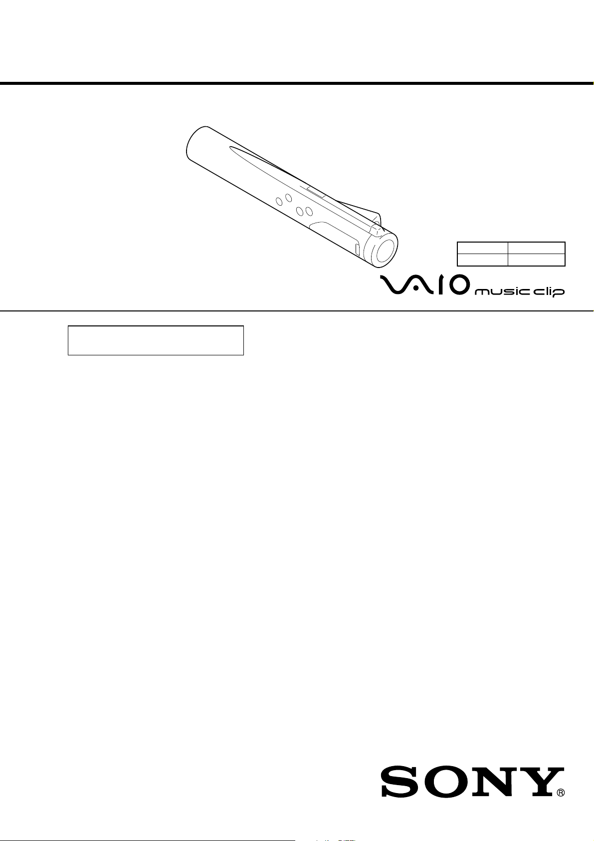
1. From the PC, start “VMC_TEST” (J-2500-377-1) of the service tool.
2. Confirm that the following screen appears.
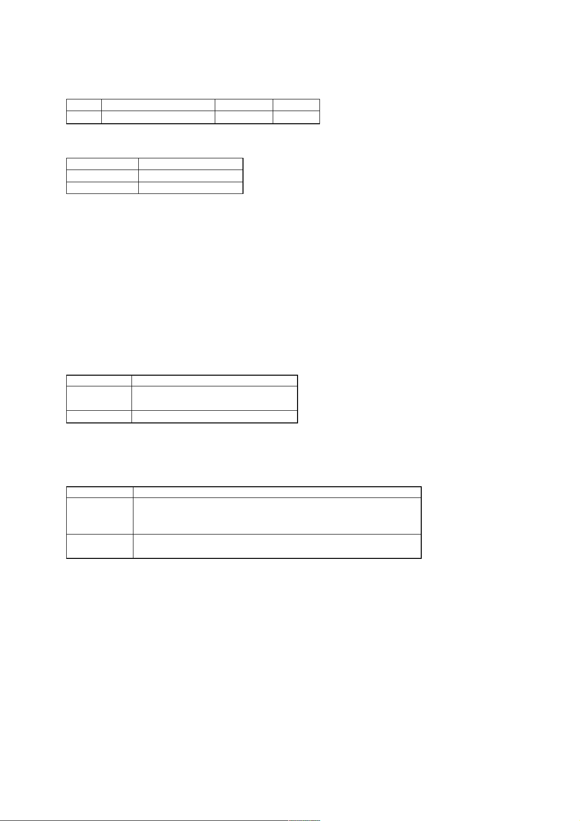
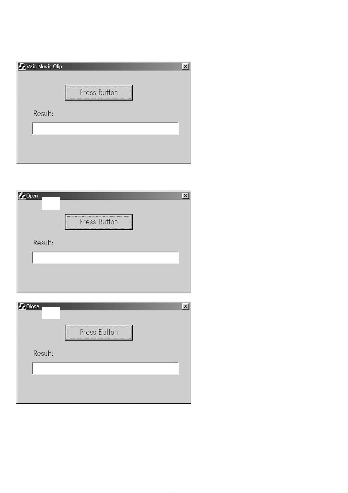
3. Connect the set with an exclusive cable. At this time, make sure that “Open” is displayed at the part 1 of the following screen.
The “Open” display means that the set is connected to PC normally (“Close” is displayed when the set is disconnected). Also, confirm
that the “PC” is displayed on the LCD of the set.
1
1
1-2
Page 5
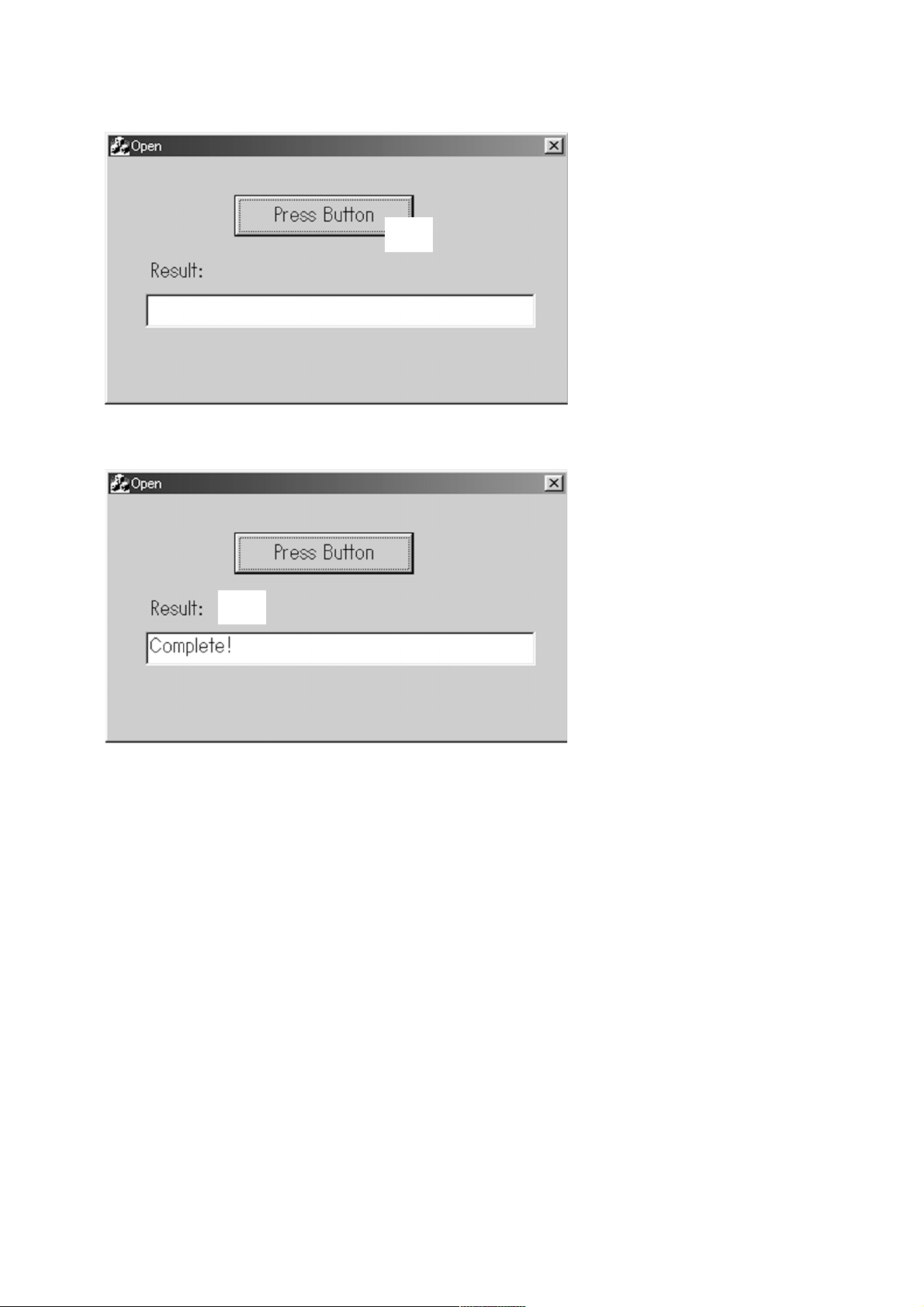
4. Click the “Press Button” at the part 2 of the following screen.
2
5. Check that, after several seconds, “Complete!” is displayed in the “Result” field at the part 3 of the following screen. Also, check that
“1 PC” is displayed on the LCD of the set.
3
Precautions
1. Never disconnect the cable during work.
2. If the PC is hung up during work, disconnect the cable and close the “VMC_TEST” once, and then retry from the beginning.
3. After the work, make sure that the check-in and check-out can be executed using the PC application “OpenMG Jukebox”. Also,
confirm that the checked out data can be played normally.
1-3. System Requirements
•IBM PC/AT and compatibles
CPU: MMX
above recommended)
Hard disk drive space: 20 MB and above (Free space is required,
depending on the version of Windows 98 and the size of the audio
data you are using.)
RAM: 64 MB and above
CD-ROM drive
Sound Board: Creative SoundBlaster 16 compatible
Default built-in USB port
• Operating system: The default installation of Windows
version (The product does not work on Windows 95/3.1 or Windows
NT. Not assured trouble-free if you use an upgrade version from
Windows 95/3.1 to Windows 98.)
• Display: SVGA (800 × 600 pixel) (supports High Color (16 bit) and
above)
• Internet access
Pentium 233 MHz and above (Pentium II 400 MHz and
98 English
1-3
Page 6
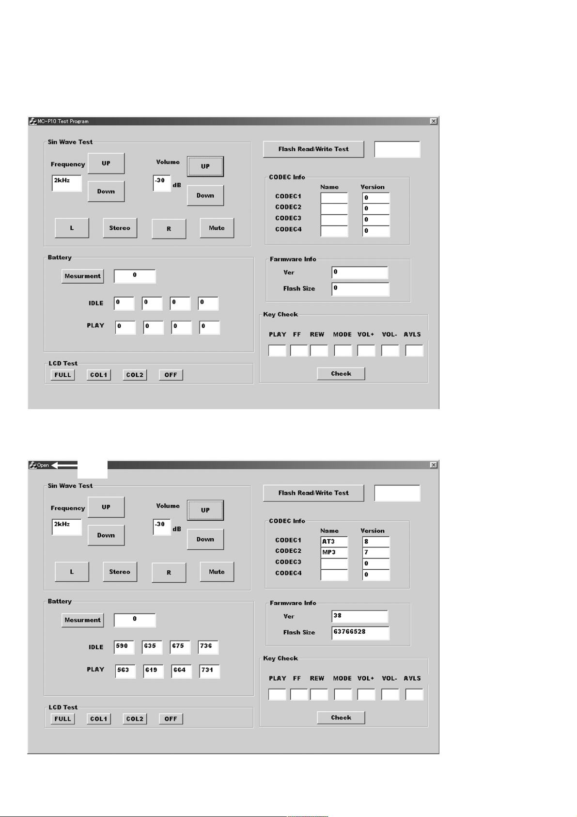
1-4. Test Mode
This set has the T est mode in the microcomputer , and the use of e xclusive application softw are on the PC side can check various functions.
Preparation
1. From the PC, start the T est mode “Vmo_Check.e xe” (J-2500-377-1) of the sevice tool, and confirm that the following screen appears.
2. Connect the set with exclusive cable (the po wer for the set is supplied from USB), then check that the part 1 on the following screen
is “Open”, and also “1 PC” is displayed on the LCD of the set. (Part 1 becomes “Close” if disconnecting the cable again.) At this time,
a sine wave is generated from the headphone.
1
Supplement: If the part 1 does not become “Open”, the USB of the set will be faulty.
Also, audio signals are outputted from the reference signal in the DSP of the set.
1-4
Page 7
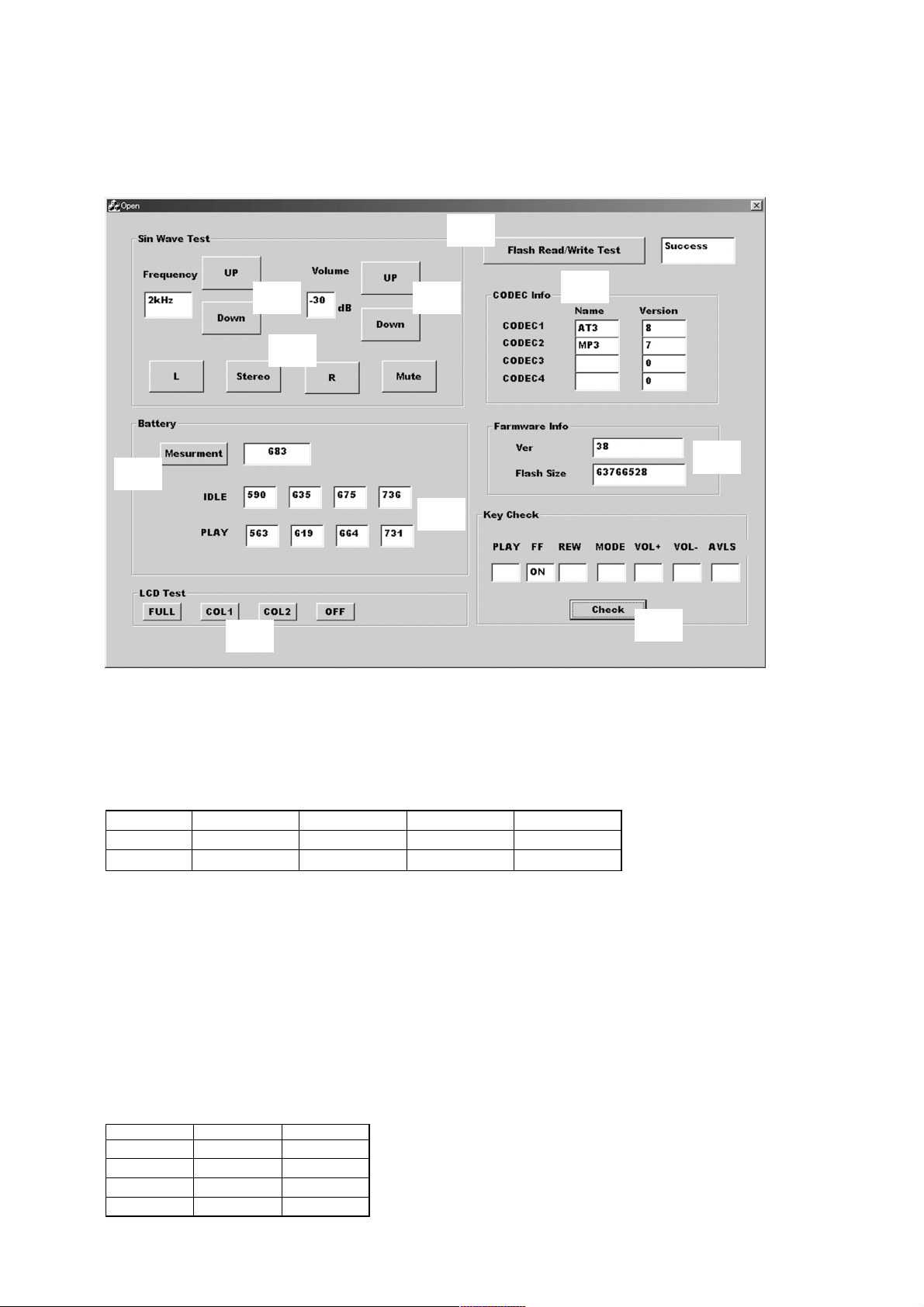
Description of Service Mode Operation
1. Checking the Functions of Audio Section
Clicking the Up/Down at part 2 of the screen can change the output frequency. Also, clicking the Up/Down at part 3 can change the
volume. Clicking the L/Stereo/R/Mute at part 4 can change the output.
8
2 3
9
4
0
6
5
7
2. Battery Threshold Value Reading and Measurement
When the Test mode is selected, the threshold values for the remaining battery capacity written in the set are displayed at the part 5.
These values are adjusted values at the shipment, and inherent data.
The threshold values are provided separately for the PLAY and for the IDLE; values are at scale 3→4, scale 2→3, scale 1→2, and OFF
from the right to left.
Standard threshold value is given with “1024/1.8 × Battery T erminal Voltage”, and the battery terminal voltages to respective threshold
values are as follows.
qa
OFF Scale 1→2 Scale 2→3 Scale 3→4
At idle 1.05 V 1.13 V 1.20 V 1.31 V
At play 1.00 V 1.10 V 1.18 V 1.30 V
Click the part 6, and the calculated value corresponding to the voltage will be displayed if the voltage is applied to the battery terminals.
For example, if 1.2 V is applied to the battery terminals, approximate 680 is displayed.
3. LCD Test
Clicking the FULL/COL 1/COL 2/OFF respectively at part 7 can cause the LCD on the set to turn on full LCD, column 1, column 2,
or turn off LCD.
4. Flash Memory Read/Write Check
Clicking the part 8 can check the read/write of the flash memory. If normal, “Success” is displayed.
5. CODEC Info Check
The CODEC program versions written in the set can be checked, and they are displayed when the Test mode is selected (part 9). At
the shipment, they are as follows (these values vary when the progr ams are updated).
Name Version
CODEC1 AT3 8
CODEC2 MP3 7
CODEC3 blank 0
CODEC4 blank 0
1-5
Page 8

Supplement: As the CODEC Info has been written in the EEPROM on the Sub board, it may be said that the EEPROM operation is OK,
if the information is displayed normally.
6. Firmware Info Check
The microcomputer program version and the flash memory capacity can be checked, and they are displayed when the Test mode is
selected (part 0).
At the shipment, they are as follows (these values var y when the program is updated).
Ver (microcomputer version) 38
Flash Size 63766528
7. Key Check
Click the part qa with any key on the set pressed, and “ON” will be displayed in the field corresponding to that key.
1-6
1-6 E
Page 9
SECTION 2
DIAGRAMS
MC-P10
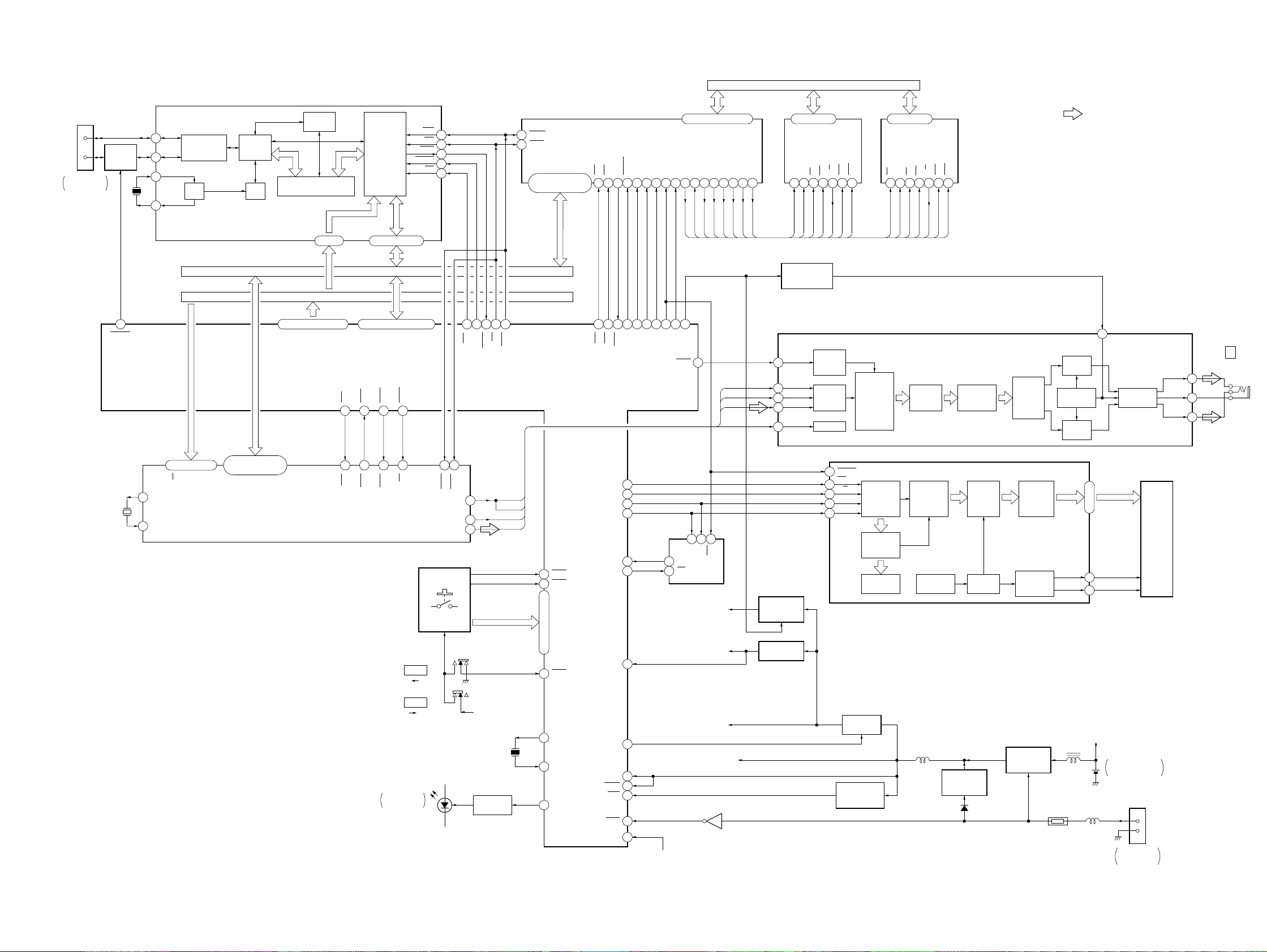
2-1. BLOCK DIAGRAM
CN901
(1/2)
2
D–
D+
3
USB
CONNECTOR
USB
SWITCH
Q901
63
TEND1
X901
48MHz
D–
2
D+
1
XIN
6
XOUT
7
USB
TRANSCEIVER
OSC DPLL
PROTCOL
USB
CONTROLLER
IC901
ENGIN
STATUS/
CONTROL
END POINT FIFO/
8BYTE SET-UP REGISTER
A7 – A0
25 – 32 35 – 38, 41 – 44
ADDRESS BUS
2 – 5, 7 – 10, 21 – 23
APPLICATION
INTERFACE
D15 – D8
DATA BUS
34 – 37, 39 – 46, 48 – 51
D0 – D15A0 – A7, A17 – A19
CS4
IRQ2
BACK
88873060
BREQ
WR
INTR
RESET
ADDRESS/DATA BUS FOR FLASH MEMORY
• SIGNAL PATH
R OUT
SWITCH
REFERENCE
SOURCE
L OUT
SWITCH
: PLAYBACK
25
VREF
HEADPHONE
AMP
VOR
VCOM
VOL
CN301
i
(HEADPHONE)
27
2
3
3 – 6, 9 – 1274, 75, 77 – 80, 82, 83
IO0 – IO7F_D_A0 – F_D_A7
OE
SC
2 13 17 19 20 24 26
F_OE
F_SC
AUIDO
ON/OFF SWITCH
Q664
MUTE
16
BCK
7
WS
8
DATA
9
SYSCLK
12
FLASH MEMORY
(LONG LEAD)
IC202
RES
R/B
WE
CE
F_CE0
F_WE
F_R/B
F_RST
VOLUME/
SOUND
CONTROL
SERIAL
DATA
INPUT
TIMING
CDE
F_CDE
SOFT MUTE/
D0 – D15
90 – 92, 94 ,96
CPU
IC801
FLASH MEMORY
CONTROLLER
IC201
CE13CE2
INTRQ
RESET98A0
4
113
105
117 118 29 70 108 107 106 71 80 69
CS3
CS2
IRQ3
TIOCB3
PORST22XIN57F_RSTB58F_RDY59F_CEB_060F_CEB_168F_CED_AB70F_WE_A0B72F_SC_A084F_OE_A0B
100A1102A218
F_RST
F_R/B
F_CE0
F_CE1
TIOCB1
TIOCA2
PF7/
TIOCA3
IRQ4
TIOCC3
89
TIOCA1
F_CDE
BCLK
LRCK
SDATA
ACLK
F_WE
F_SC
F_OE
10
RD
9
12
11
CS
8
119 105
31 83 84
CS1
TRQ1
TIOCB2
IOWR
117
IORD
120
5 – 7, 9 – 15, 88,
RD
HWR
VOLUME/
SOUND
CONTROL
&
FILTER
STAGE
3 – 6, 9 – 12
IO0 – IO7
FLASH MEMORY
(SHORT LEAD)
IC203
SC
OE
2 13 17 19 20 24 26
F_OE
F_SC
CE
F_CE1
F_WE
LINEAR
INTER-
POLATOR
WE
RES
R/B
F_R/B
F_RST
D/A CONVERTER,
HEADPHONE AMP
CDE
F_CDE
IC605
8 X OVER-
SAMPLING
FILTER
NOISE
SHAPER
&
DATA
ENCODER
X601
16.9344MHz
05
96
97
X1
X2/CLKIN
18, 39, 46, 62
HP/W
HCNTL0
HCNTL1
HBIL
6, 58, 69, 81
95, 120, 124 ,135
HD0 – HD7
DIGITAL SIGNAL
PROCESSOR
IC601
HCS
HINT
D401, 404, 405
98645117
RS
INTO
S813
AVLS
LIMIT NORM
S815
HOLD
OFF HOLD
LCD
BACK LIGHT
127129
HDS2
BCLKX0
BFSX0
BDX0
S805 – 810
HDS1
48
53
59
V1
X801
12MHz
LED DRIVE
Q404
BCLK
ACLK
LRCK
SDAT
|
VBATT
SEG0
ı
SEG14
LIQUID
CRYSTAL
DISPLAY
COM0
COM1
DRY BATTERY
SIZE "AA"
IEC DESIGNATION
R6
1PC. 1.5V
CN901
(2/2)
1
VBUS
GND
4
USB
CONNECTOR
16
RESET
TIOCA5
65
SCK1
58
TXD0
53
SCK0
57
578
SI
WP
SCK
RXD0
55
TIOCA4
VREF
TIOCB5
NMI
STBY
RES
IRQ0
R45/AN5
67
94
64
74
75
73
32
100
IRQ7
28
IRQ6
27
11
|
14
A8
|
•
16
A13
•
17
IRQ5
26
XTAL
77
EXTAL
78
TIOCB4
66
SO
4
EEPROM
CS
3
IC803
HEADPHONE AMP (IC605)
B+
DIGITAL SIGNAL PROCESSOR
(IC601) B+
V2
FLASH MEMORY CONTROLLER (IC201),
FLASH MEMORY (IC202, 203),
LED DRIVER (IC501),
DIGITAL SIGNAL PROCESSOR (IC601),
D/A CONVERTER (IC605),
EEPROM (IC803),
USB CONTROLLER (IC901)
B+
V1
CPU (IC801)
B+
Q102
VBATT
+2.8V
REGULATOR
IC103
REGULATOR
IC104
CS
10
C/D
11
SI
9
CK
8
RESET SIGNAL
INTERFACE
COMMAND/
REGISTER
COMMAND
DECODER
B+ SWITCH
Q103
GENERATOR
IC107
SERIAL
DATA
ADDRESS
COUNTER
TIMING
GENERATOR
L103
DISPLAY
COMMON
COUNTER
LCD DIRVER
IC501
+3.2V
REGULATOR
IC102
D103
DATA
RAM
LCD
SEGMENT
DRIVER
LCD
COMMON
DRIVER
SWITCHING
REGULATOR
IC101, Q101
THP501
SEG0
ı
SEG14
COM0
COM1
L101
17
31
12
13
L102
2-1 2-2
Page 10

2-2. NOTE FOR PRINTED WIRING BOARDS AND SCHEMATIC DIAGRAMS
Note on Printed Wiring Board:
• X : parts extracted from the component side.
• Y : parts extracted from the conductor side.
• b : Pattern from the side which enables seeing.
(The other layers' patterns are not indicated.)
Caution:
Pattern face side: Parts on the pattern face side seen from
(Conductor Side) the pattern face are indicated.
Parts face side: Parts on the parts face side seen from
(Component Side) the parts face are indicated.
• MAIN and SUB boards are multi-layer printed board.
However, the patterns of intermediate-layer hav e not been included in the diagram.
Note on Schematic Diagram:
• All capacitors are in µF unless otherwise noted. pF: µµF
50 WV or less are not indicated except for electrolytics
and tantalums.
• All resistors are in Ω and 1/
specified.
• % : indicates tolerance.
f
•
• C : panel designation.
• U : B+ Line.
• Power voltage is dc 1.5 V and fed with regulated dc power
• Voltages and wav ef orms are dc with respect to ground in
• Voltages are taken with a VOM (Input impedance 10 MΩ).
• Waveforms are taken with a oscilloscope.
• Circled numbers refer to waveforms.
• Signal path.
: internal component.
supply from battery terminal.
playback mode.
no mark : PLAYBACK
Voltage var iations may be noted due to normal produc-
tion tolerances.
Voltage var iations may be noted due to normal produc-
tion tolerances.
F : PLAYBACK
4
W or less unless otherwise
• Semiconductor
Location
– Component Side –
Ref. No. Location
D101 A-1
D102 A-1
D811 A-2
D812 A-2
IC101 A-1
IC102 A-1
IC202 A-5
IC203 A-5
Q101 A-2
• Semiconductor
Location
– Conductor Side –
Ref. No. Location
D103 A-1
D810 A-4
IC104 A-2
IC107 A-4
IC201 A-5
IC601 A-3
IC801 A-3
IC901 A-1
Q102 A-1
Q103 A-4
Q901 A-1
2-3
2-4
Page 11

2-3. PRINTED WIRING BOARD – MAIN Board –
MC-P10
2-5
(Page 2-11)
2-6
Page 12

MC-P10
2-4. SCHEMATIC DIAGRAM – MAIN Board (1/2) – • See page 2-15 for Waveforms. • See page 2-16 for IC Block Diagrams.
(Page 2-13)
2-7
2-8
Page 13

2-5. SCHEMATIC DIAGRAM – MAIN Board (2/2) – • See page 2-15 for Waveforms. • See page 2-16 for IC Block Diagrams.
MC-P10
2-9
2-10
Page 14

MC-P10
2-6. PRINTED WIRING BOARD – SUB Board –
(Page 2-5)
• Semiconductor Location
– Component Side –
Ref. No. Location
D601 A-2
D602 A-1
D603 A-1
D802 A-4
D803 A-4
IC803 A-2
1- 677 - 091-
11
1- 677 - 092-
11
JACK FLEXIBLE BOARD
L601
L602
R662
R661
S815
HOLD
OFF , HOLD
S813
AVLS
NORM , LIMIT
CN301
i
(HEADPHONE)
• Semiconductor Location – Conductor Side –
D401 A-3
D404 A-4
D405 A-4
D801 A-5
D804 A-3
D805 A-3
Ref. No. LocationRef. No. Location
D806 A-5
D807 A-2
D808 A-2
D809 A-5
IC103 A-2
Ref. No. Location
IC501 A-2
IC605 A-1
Q404 A-5
Q664 A-2
D401, 404, 405
(LCD BACK LIGHT)
1
9
1- 677 - 093 -
11
2-11
2-12
Page 15

2-7. SCHEMATIC DIAGRAM – SUB Board – • See page 2-15 for Waveforms. • See page 2-17 for IC Block Diagrams.
MC-P10
(Page 2-8)
2-13
2-14
Page 16

• Waveforms
– MAIN Board –
1 IC901 7 XOUT
48 MHz
2 IC801 uj XTAL
3.1 Vp-p
6 IC601 td BFSX0
22.8 µs
7 IC601 oj X2/CLKIN
3.3 Vp-p
– SUB Board –
1 IC501 1 OSC1
34.2 µs
2 IC605 7 BCK
3.4 Vp-p
• IC Block Diagrams
– MAIN Board –
IC101 MAX1674EUA-TG069
MINIMUM
OFF-TIME
ONE-SHOT
Q
TRIG
ONE-SHOT
ERROR
LBI
LBO
REF
FB
2
3
4
–
+
–
+
LOW-BATTERY
COMPARATOR
REFERENCE
TRIG
AMP
1
MAXIMUM
ON-TIME
OFF-SHOT
ONE-SHOT
S
Q
ZERO CROSSING
AMP
F/F
Q
R
CURRENT-LIMIT
AMP
–
+
EN
+
–
8
OUT
7
LX
6
GND
5
SHDN
12 MHz
3 IC801 i; PF7/
12 MHz
4 IC201 ws XIN
3 Vp-p
3 Vp-p
3 Vp-p
16.9344 MHz
1 Vp-p
356 ns
3 IC605 8 WS
22.8 µs
3.5 Vp-p
3.3 Vp-p
IC202, 203 HN29W25611TBE-50
SECTOR
VCC
I/O 0
I/O 3
VSS
VCC
I/O 4
I/O 7
VSS
ADDRESS
1
OE
2
3
ı
ı
6
7
MULTIPLEXER
8
9
ı
ı
12
SC
13
14
BUFFER
READ/PROGRAM/ERASE
X-DECODER 1638 X (2048 + 64) X 8
DATA
INPUT
BUFFER
CONTROL
INPUT
DATA
CONTROL
Y-ADDRESS
COUNTER
MEMORY MATRIX
DATA REGISTOR (2048 + 64)
Y-GATING
Y-DECODER
CONTROL
SIGNAL
BUFFER
DATA
OUTPUT
BUFFER
28
27
26
25
24
23
22
21
20
19
18
17
16
15
VSS
NC
CDE
NC
RES
NC
VCC
VSS
RDY/BUSY
WE
NC
CE
NC
VCC
12 MHz
5 IC601 rk BCLKX0
356 ns
3.5 Vp-p
2-15
2-16
Page 17

IC901 ML60851CLBZ060
1 3233 31 30 29 28 27 26 25 24 23
DREQ
34
AD7
35
AD6
36
AD5
AD4
GND
VCC5
AD3
AD2
AD1
AD0
37
38
39
40
41
42
43
44
END POINT FIFO/
8BYTE SET-UP
REGISTER
PROTOCOL
ENGINE
USB
TRANSCEIVER
DACK
A0
STATUS/
CONTROL
DPLL
OSC
A2
A1
A5
A4
A3
APPLICATION
INTERFACE
ALE
ADSEL
A7
A6
D8
22
D9
21
D10
20
D11
19
VCC5
18
GND
17
D12
16
D13
15
D14
14
D15
13
INTR
12
1 2
D+
D–
– SUB Board –
IC501 BU9728AKV-E2
OSC1
1
OSC2
VSS
VDD
SCK
C/D
V1
V2
V3
SD
CS
10
11
GENERATOR
2
3
LCD DRIVER
BIAS CIRCUIT
4
5
6
7
8
9
INTERFACE
COMMAND/DATA
REGISTER
TIMING
SERIAL
COMMON
COUNTER
COMMON
ADDRESS
COUNTER
3 4 5 6 7 8 9 10 11
CS
VCC3
LCD
DRIVER
4BITS
TEST1
TEST2
XIN
XOUT
DISPLAY DATA RAM
RD
(DD RAM)
WR
RESET
ı
SEG31
48 – 17
LCD
SEGMENT
DRIVER
32BITS
SEG0
RESET
16
COM3
15
COM2
14
COM1
13
COM0
12
COMMAND
DECODER
2-17
Page 18

IC605 TDA1548TZ/N1.518
VSSO
VCOM
VOL
FILTCL
MODE0
MODE1
BCK
DATA
VDDD
VSSD
SYSCLK
WS
OP2
1
OP3
OP1
RCONV1
TIMING
+
–
+
–
8 X OVERSAMPLING
(SAMPLE-AND-HOLD)
NOISE SHAPER
16 (4-bit)
CALIBRATED
CURRENT
SOURCES
OUTPUT
SWITCHES
16 (4-bit)
CALIBRATED
CURRENT
2
3
4
5
6
7
8
9
10
11
12
IF1
13
IF2
14
SOFT MUTE CONTROL
LINEAR INTERPOLATOR
2nd ORDER
DATA
ENCODRE
LEFT
SINKS
SERIAL DATA INPUT
VOLUME CONTROL
SOUND CONTROL
FILTER STAGE 1
FILTER STAGE 2
8 X OVERSAMPLING
(SAMPLE-AND-HOLD)
REFERENCE
SOURCE
2nd ORDER
NOISE SHAPER
DATA
ENCODRE
16 (4-bit)
CALIBRATED
CURRENT
SOURCES
RIGHT
OUTPUT
SWITCHES
16 (4-bit)
CALIBRATED
CURRENT
SINKS
1fs
2fs
4fs
8fs
VOLUME
SOUND
CONTROL
+
–
RCONV2
VDDA
VSSA
AND
VDDA
–
+
OP4
VSSA
VDDO
28
VOR
27
FILTCR
26
VREF
25
VSSA
24
VDDA
23
AD3S
22
ADVC
21
ADBB
20
ADTR
19
ADREF
18
CLSEL
17
MUTE
16
DEEM
15
IC803 25LC640XT-I/ST
STATUS
REGISTER
I/O CONTROL
LOGIC
1 2 3 4 5 6 7 8
CS
SO
VCC
HOLD
MEMORY
CONTROL
LOGIC
WP
VSSSISCK
HV GENERATOR
X DEC
Y DECODER
SENSE AMP
R/W CONTROL
EEPROM
ARREY
PAGE
LATCHES
2-18
Page 19

2-8. IC PIN FUNCTION DESCRIPTION
• MAIN BOARD IC201 HN29W256H02TE-1 (FLASH MEMORY CONTROLLER)
Pin No. Pin Name I/O
1 ATSEL I
2 A10 I
3, 4 CE2, CE1 I
5 D15 I/O
6D7
7 D14
8 GND
9D6
10 D10
11 D05
12 D12
13 D4
14 D11
15 D3 I/O
16 VDD
17 TEST1
18 PORST
19, 20 TEST2, TEST3
21 GND
22 XIN
23 XOUT
24 GND
25 VDD
26 to 33 TEST4 to TEST11 I
34 GND —
35, 36 TEST12, TEST13
37 F CDE BB
38, 39
F WE B0B,
I/O Two-way data bus with the CPU(IC801)
I/O
— Ground terminal
I/O
I/O
I/O
I/O Two-way data bus with the CPU(IC801)
I/O
I/O
— Ground terminal
O System clock output terminal Not used (open)
— Ground terminal
— Power supply terminal (+3.1V)
O Command data enable signal output terminal Not used (open)
O Write enable signal output terminal Not used (open)
Description
Not used (fixed at “L”)
Address signal input terminal Not used (fixed at “L”)
Chip select signal input from the CPU(IC801)
I Power supply terminal (+3.1V)
I Test signal input terminal Not used (fixed at “H”)
I Reset signal input from the CPU(IC801) “L”: reset
I Test signal input terminal Not used (open)
I System clock input from the CPU(IC801)
Test signal input terminal Not used (open)
Ground terminal
I Test signal input terminal Not used (open)
40, 41 F SC B0, F SC B1
42 to 45 F D B7 to F D B4
46 VDD
47 TEST14
48 GND
49 VDD
50 F D B3
51 GND
52 to 54 F D B2 to F D B0 I/O
55, 56
57 F RSTB
58 F RDY
59 F CEB 0
60 F CEB1
61 to 64 F CEB 2 to F CEB 5
65 GND
F OE B0B,
F OE B1B
O Serial data clock output terminal Not used (open)
I/O Two-way data bus Not used (open)
— Power supply terminal (+3.1V)
— Ground terminal
— Power supply terminal (+3.1V)
I/O Two-way data bus Not used (open)
— Ground terminal
O Enable signal output terminal Not used (open)
O Reset signal output to the flash memory (IC202, 203) “L”: reset
O Chip enable signal output to the flash memory (IC202) “L” active
O Chip enable signal output to the flash memory (IC203) “L” active
O Chip enable signal output terminal Not used (open)
— Ground terminal
I Test signal input terminal Not used (open)
Two-way data bus Not used (open)
I Ready signal input from the flash memory (IC202, 203) “H”: ready
2-19
Page 20

Pin No. Pin Name I/O
66, 67 F CEB 6, F CEB7
68 F CDE AB
69 GND
70 F WE A0B
71 F WE A1B
72 F SC A0
73 F SC A1 O
74, 75 F D A7, F D A6
76 VDD
77 to 80 F D A5 to F D A2
81 GND
82, 83 F D A1, F D A0
84 F OE A0B
85 F OE A1B
86 TEST15
87 VCC
88 D10
89 IOIS16
90 D9
91 D2
92 D8
93 GND
94 D1
95 PDIAG
96 D0
97 DASP
98 A0 I
99 REG
100 A1 I
101 INPACK
102 A2 I
103 IORDY
104 A3 I
105 RESET
106 VCC
107, 108 A4, A5
109 CSEL
110 TEST16
111 GND
112 A6 I
113 INTRQ
115 WE
116 A8 I
117 IOWR
118 GND
119 A9 I
120 IORD
O Chip enable signal output terminal Not used (open)
O Command data enable signal output to the flash memory (IC202, 203) “L” active
— Ground terminal
O Write enable signal output to the flash memory (IC202, 203) “L” active
O Write enable signal output terminal Not used (open)
O Serial data clock output to the flash memory (IC202, 203)
I/O Two-way data bus with the flash memory (IC202, 203)
— Power supply terminal (+3.1V)
I/O Two-way data bus with the flash memory (IC202, 203)
— Ground terminal
I/O Two-way data bus with the flash memory (IC202, 203)
O Enable signal output to the flash memory (IC202, 203) “L” active
O Enable signal output terminal Not used (open)
— Power supply terminal (+3.1V)
I/O Two-way data bus with the CPU(IC801)
O Not used (open)
I/O
I/O Two-way data bus with the CPU(IC801)
I/O
— Ground terminal
I/O Two-way data bus with the CPU(IC801)
— Not used (open)
I/O Two-way data bus with the CPU(IC801)
— Not used (open)
O Not used (open)
O Reset signal output to the CPU (IC801) “L”: reset
— Power supply terminal (+3.1V)
— Ground terminal
O Interrupt request signal output to the CPU (IC801)
— Ground terminal
Description
Serial data clock output terminal Not used (open)
I Test signal input terminal Not used (open)
Address signal input from the CPU(IC801)
Not used (open)
I
Address signal input from the CPU(IC801)
I Not used (open)
Address signal input from the CPU(IC801)
Address signal input terminal Not used (fixed at “L”)
I Address signal input terminal Not used (fixed at “L”)
I Not used (fixed at “L”)
I Test signal input terminal Not used (open)
Address signal input terminal Not used (fixed at “L”)
I Not used (fixed at “H”)
Address signal input terminal Not used (fixed at “L”)
I Write enable signal input from the CPU (IC801)
Address signal input terminal Not used (fixed at “L”)
I Read enable signal input from the CPU (IC801)
2-20
Page 21

• MAIN BOARD IC601 TMX320VC5409GGU100 (DIGITAL SIGNAL PROCESSOR)
Pin No. Pin Name I/O
1CVSS—
2 A22 I
3CVSS—
4 DVDD —
5 A10 I
6HD7
7 to 11 A11 to A15
12 CVDD
13 HAS
14 DVSS
15 CVSS —
16 CVDD
17 HCS
18 HR/W
19 READY
20 PS
21 DS
22 IS
23 R/W
24 MSTRB
25 IOSTRB
26 MSC O
27 XF O
28 HOLDA O
29 IAQ O
30 HOLD I
31 BIO I
32 MP/MC I
33 DVDD —
34 CVSS
35 BDR1
36 BFSR1
37 CVSS
38 BCLKR1
39 HCNTL0
40 DVSS
41, 42 BCLKR0, BCLKR2
43, 44 BFSR0, BFSR2
45 BDR0
46 HCNTL1
47 BDR2
48 BCLKX0
49 BCLKX2
50 CVSS
51 HINT
I/O Two-way data bus with the CPU (IC801)
— Power supply terminal (+1.8V)
— Ground terminal
— Power supply terminal (+1.8V)
O Program space select signal output terminal Not used (open)
O Data space select signal output terminal Not used (open)
O I/O space select signal output terminal Not used (open)
O Read/write signal output terminal Not used (open)
O Memory strobe signal output terminal Not used (open)
O I/O strobe signal output terminal Not used (open)
— Ground terminal
— Ground terminal
— Ground terminal
O Clock output to the D/A converter (IC605)
O Clock output terminal (fixed at “H”)
— Ground terminal
O Interrupt signal output to the CPU (IC801)
Description
Ground terminal
Address signal input terminal Not used (open)
Ground terminal
Power supply terminal (+3.1V)
Address signal input terminal Not used (open)
I Address signal input terminal Not used (open)
I Address strobe signal input terminal (fixed at “H”)
Ground terminal
I Chip select signal input from the CPU (IC801)
I Address signal input from the CPU (IC801)
I Data ready signal input terminal (fixed at “H”)
Microstate complete signal output terminal Not used (open)
External flag signal output terminal Not used (open)
Hold acknowledge signal output terminal Not used (open)
Instruction acquisition signal output terminal Not used (open)
Hold signal input terminal (fixed at “H”)
Branch control signal input terminal (fixed at “H”)
Mode select signal input terminal (fixed at “L”)
Power supply terminal (+3.1V)
I Serial data receive signal input terminal (fixed at “H”)
I Frame synchronization pulse signal input terminal (fixed at “H”)
I Data receive clock input terminal (fixed at “H”)
I Address signal input from the CPU (IC801)
I Data receive clock input terminal (fixed at “H”)
I Frame synchronization pulse signal input terminal (fixed at “H”)
I Serial data receive signal input terminal (fixed at “H”)
I Address signal input from the CPU (IC801)
I Serial data receive signal input terminal (fixed at “H”)
2-21
Page 22

Pin No. Pin Name I/O
52 CVDD —
53 BFSX0 O
54 BFSX2 O
55 HRDY
56 DVDD —
57 DVSS
58 HD0
59 BDX0
60 BDX2
61 IACK
62 HBIL
63 NMI
64 INT0
65 to 67 INT1 to INT3
68 CVDD —
69 HD1
70 CVSS
71 BCLKX1
72 DVSS
73 BFSX1 O
74 BDX1
75 DVDD
76 DVSS
77 CLKMD1
78 CLKMD2
79 CLKMD3
80 NC
81 HD2
82 TOUT
83 EMU0
84 EMU1/OFF
85 TDO
86 TDI
87 TRST
88 TCK
89 TMS
90 CVSS
91 CVDD —
92 HPIENA
93 DVSS
94 CLKOUT
95 HD3
96 X1
97 X2/CLKIN
98 RS
99 to 104 D0 to D5
I/O Two-way data bus with the CPU (IC801)
I/O Two-way data bus with the CPU (IC801)
I/O Two-way data bus with the CPU (IC801)
I/O Two-way data bus with the CPU (IC801)
I/O Two-way data bus Not used (open)
Description
Power supply terminal (+1.8V)
LR frame signal output to the D/A converter (IC605)
Serial data receive signal output terminal Not used (fixed at “H”)
O Ready signal output terminal Not used (open)
Power supply terminal (+3.1V)
— Ground terminal
O Serial data transmit signal output to the D/A converter (IC605)
O Serial data transmit signal output terminal Not used (open)
O Interrupt request signal output terminal
I Address signal input from the CPU (IC801)
I Nonmaskable interrupt request signal input terminal (fixed at “H”)
I Interrupt request signal input from the CPU (IC801)
I Interrupt request signal input terminal (fixed at “H”)
Power supply terminal (+1.8V)
— Ground terminal
O Clock out put terminal (fixed at “H”)
— Ground terminal
Serial data receive signal output terminal (fixed at “H”)
O Serial data transmit signal output terminal Not used (open)
— Power supply terminal (+3.1V)
— Ground terminal
I Clock mode signal output terminal (fixed at “L”)
I Clock mode signal output terminal (fixed at “H”)
I Clock mode signal output terminal (fixed at “L”)
— Not used (open)
O Timer signal output terminal Not used (open)
I Emulator signal input terminal (fixed at “H”)
O Emulator signal output terminal (fixed at “H”)
O Test data signal output terminal
I Test data signal input terminal
I Test reset signal input terminal
I Test clock input terminal
I Test mode select signal input terminal
— Ground terminal
Power supply terminal (+1.8V)
I HPI module select signal input terminal (fixed at “H”)
— Ground terminal
O Master clock output terminal
O System clock output terminal (16.9344MHz)
I System clock input terminal (16.9344MHz)
I Reset signal input to the CPU (IC801) “L”: reset
2-22
Page 23

Pin No. Pin Name I/O
0
4
105 A16
106 DVSS
107 to 11
111 CVSS
112 DVDD
113 to 119 D6 to D12
120 HD4
121 to 123 D13 to D15
124 HD5
125 CVDD —
126 CVSS
127 HDS1
128 DVSS
129 HDS2
130 DVDD
131 to 13
135 HD6
136 to 141 A4 to A9
142 CVDD —
143 A21
144 DVSS
A17 to A20
A0 to A3
Description
I Address signal input terminal Not used (open)
— Ground terminal
I Address signal input terminal Not used (open)
— Ground terminal
— Power supply terminal (+3.1V)
I/O Two-way data bus Not used (open)
I/O Two-way data bus with the CPU (IC801)
I/O Two-way data bus Not used (open)
I/O Two-way data bus with the CPU (IC801)
Power supply terminal (+1.8V)
— Ground terminal
I Data read signal input from the CPU (IC801)
— Ground terminal
I Data write signal input from the CPU (IC801)
— Power supply terminal (+3.1V)
I Address signal input terminal Not used (open)
I/O Two-way data bus with the CPU (IC801)
I Address signal input terminal Not used (open)
Power supply terminal (+1.8V)
I Address signal input terminal Not used (open)
— Ground terminal
2-23
Page 24

• MAIN BOARD IC801 HD6432328A05TE (CPU)
Pin No. Pin Name I/O
1 VCC —
2A0O
3 to 5 A1 to A3 O
6 VSS
7 to 10 A4 to A7
11 A8
12 A9
13 A10
14 A11
15 VSS —
16 A12
17 A13
18 to 20 A14 to A16
21 to 23 A17 to A19
24 VSS
25 IRQ4
26 IRQ5 I
27 IRQ6
28 IRQ7
29 IRQ3
30 IRQ2
31 IRQ1 I
32 IRQ0
33 VCC —
34 to 37 D0 to D3
38 VSS
39 to 42 D4 to D7
43 to 46 D8 to D11
47 VSS
48 to 51 D12 to D15
52 VCC —
53 TXD0
54 TXD1
55 RXD0
56 RXD1
57 SCK0
58 SCK1
59 VSS
60 CS4
61 TEND0
62 DREQ1
63 TEND1
64 TIOCB5
65 TIOCA5
66 TIOCB4
Power supply terminal (+3.1V)
Address signal output to the digital signal processor (IC601) and USB controller (IC901)
Address signal output to the USB controller (IC901)
— Ground terminal
O Address signal output to the USB controller (IC901)
I Hs key (S805) input terminal
I L key (S806) input terminal
I l key (S807) input terminal
I MODE key (S808) input terminal
Ground terminal
I VOL + key (S809) input terminal
I VOL - key (S810) input terminal
O Address signal output terminal Not used (open)
O Address signal output to the digital signal processor (IC601)
— Ground terminal
I Test mode signal input terminal “L”: test mode
AVLS switch (S813) input terminal
I Interrupt signal input from the MODE key (S808)
I Interrupt signal input from the Hs, L, l, VOL +/- key (S805 to 807, 809, 810)
I Interrupt signal input from the flash memory controller (IC201)
I Interrupt signal input from the digital signal processor (IC601)
Interrupt signal input from the USB controller (IC901)
I USB connection detect signal input terminal
Power supply terminal (+3.1V)
I/O Two-way data bus with the flash memory controller (IC201)
— Ground terminal
I/O Two-way data bus with the flash memory controller (IC201)
I/O Two-way data bus with the flash memory controller (IC201) and USB controller (IC901)
— Ground terminal
I/O Two-way data bus with the flash memory controller (IC201) and USB controller (IC901)
Power supply terminal (+3.1V)
O Serial data output to the LCD driver (IC501) and EEPROM (IC803)
O Serial data output terminal for the test mode
I Serial data input to the EEPROM (IC803)
I Serial data input terminal for the test mode
O Serial data clock output to the LCD driver (IC501) and EEPROM (IC803)
O Command/data output to the LCD driver (IC501)
— Ground terminal
O Enable signal output to the digital signal processor (IC601) “L” active
O
Not used (open)
O
O USB D+ pull up control signal output terminal “L”: ON
O Power supply (V2) control signal output terminal “L”: ON
O Chip select signal output to the LCD driver (IC501)
O LCD back light (D401, 404, 405) ON/OFF control signal output terminal “H”: LED ON
Description
2-24
Page 25

Pin No. Pin Name I/O
67 TIOCA4
68 TIOCD3
69 TIOCC3
70 TIOCB3
71 TIOCA3
72 WDTOVF
73 RES I
74 NMI
75 STBY
76 VCC
77 XTAL
78 EXTAL
79 VSS
80 PF7/
81 VCC
82 AS
83 RD
84 HWR
85 LWR
86 WAIT
87 BACK
88 BREQ
89 IRQ4
90 IRQ5
91 IRQ6
92 WAIT
93 AVCC
94 VREF
O
O Not used (open)
O Power supply control signal output to the headphone amp (IC605) “H”: ON
O Reset signal output to the flash memory controller (IC201) “L”: reset
O
O Watch dog timer mode over flow signal output terminal Not used (open)
— Power supply terminal (+3.1V)
O Main system clock output terminal (12MHz)
— Ground terminal
O System clock output to the flash memory controller (IC201)
— Power supply terminal (+3.1V)
O Address strobe signal output terminal “L” active Not used (open)
O
O
O Lower byte data write enable signal output terminal “L” active Not used (open)
O Bus wait request signal output terminal Not used (open)
O Interrupt request signal output to the digital signal processor (IC601)
O Reset signal output to the digital signal processor (IC601) “L”: reset
O Mute control signal output to the D/A converter (IC605) “L”: mute
O
O Not used (open)
O
— Power supply terminal (+3.1V)
Description
Chip select signal output to the EEPROM (IC803)
Reset signal output to the flash memory controller (IC201) , digital signal processor (IC601)
and USB controller (IC901) “L”: reset
System reset signal input from the reset signal generator (IC107) “L”: reset
For several hundreds msec. after the power supply rises, “L” is input, then it changes to “H”
I Nonmaskable interrupt request signal input terminal
I standby mode input terminal “L”: standby
I Main system clock input terminal (12MHz)
Data read signal output to the flash memory controller (IC201) , digital signal processor
(IC601) and USB controller (IC901) “L” active
Upper byte data write enable signal output to the flash memory controller (IC201) , digital
signal processor (IC601) and USB controller (IC901) “L” active
I Reference voltage input terminal
95 to 99 P40/AN0 to P44/AN4
100 P45/AN5
101, 102 DA0, DA1
103 AVSS
104 VSS
105 TIOCB2
106 TIOCA2
107 TIOCB1
108 TIOCA1
109 TIOCD0
110 TIOCC0
111 TIOCB0
112 TIOCA0
I Not used (pull up)
I Voltage detect input terminal
I Not used (pull up)
— Ground terminal
— Ground terminal
O Reset signal output to the USB controller (IC901) “L”: reset
O
O Address signal output to the flash memory controller (IC201)
O
O Not used (open)
O
O Not used (open)
O
2-25
Page 26

Pin No. Pin Name I/O
113 to 115 MD0 to MD2
116 CAS
117, 118 CS3, CS2
119 CS1
120 CS0
Description
I Operation mode control signal input terminal
O Column address strobe signal output terminal Not used (open)
O Chip select signal output to the flash memory controller (IC201)
O Chip select signal output to the USB controller (IC901)
O Chip select signal output terminal Not used (open)
2-26 E
2-26
Page 27

SECTION 3
ELECTRICAL PARTS LIST
JACK SUB
NOTE:
• Due to standardization, replacements in the
parts list may be different from the parts specified in the diagrams or the components used
on the set.
• -XX and -X mean standardized parts, so they
may have some difference from the original
one.
• RESISTORS
All resistors are in ohms.
METAL: Metal-film resistor.
METAL OXIDE: Metal oxide-film resistor.
F: nonflammable
• PC BOARD ASSY (S) : For service only
Ref. No. Part No. Description Remark Ref. No. Part No. Description Remark
22 A-7056-709-A FLEXIBLE MOUNTED PC BOARD, JACK
*******************************
(Included in SUB PC BOARD ASSY (S))
L601 1-469-526-91 INDUCTOR 22uH ±10%
L602 1-469-526-91 INDUCTOR 22uH ±10%
R661 1-218-835-11 METAL CHIP 330 0.5% 1/16W
R662 1-218-835-11 METAL CHIP 330 0.5% 1/16W
S813 1-572-922-11 SWITCH, SLIDE (AVLS)
S815 1-572-922-11 SWITCH, SLIDE (HOLD)
************************************************************
12 A-8056-772-A SUB PC BOARD ASSY (S)
*********************
(Including FLEXIBLE MOUNTED PC BOARD,
JACK and SUB MOUNTED PC BOARD)
• Items marked “*” are not stocked since they
are seldom required for routine service.
Some delay should be anticipated when ordering these items.
• SEMICONDUCTORS
In each case, u: µ, for example:
uA. . : µA. . uPA. . : µPA. .
uPB. . : µPB. . uPC. . : µPC. .
uPD. . : µPD. .
• CAPACITORS
uF: µF
• COILS
uH: µH
C806 1-125-777-11 CERAMIC CHIP 0.1uF 10% 10V
C820 1-164-937-11 CERAMIC CHIP 0.001uF 10% 16V
C821 1-164-937-11 CERAMIC CHIP 0.001uF 10% 16V
C822 1-164-937-11 CERAMIC CHIP 0.001uF 10% 16V
C823 1-164-937-11 CERAMIC CHIP 0.001uF 10% 16V
C824 1-164-937-11 CERAMIC CHIP 0.001uF 10% 16V
C825 1-164-937-11 CERAMIC CHIP 0.001uF 10% 16V
C827 1-164-939-11 CERAMIC CHIP 2200PF 10% 16V
CN102 1-794-020-21 BOARD TO BOARD CONNECTOR 40P
D401 8-719-075-56 LED FA1113F-Y641-TR (LCD BACK LIGHT)
D404 8-719-075-56 LED FA1113F-Y641-TR (LCD BACK LIGHT)
D405 8-719-075-56 LED FA1113F-Y641-TR (LCD BACK LIGHT)
D601 8-719-056-59 DIODE MAZS120008SO
D602 8-719-056-59 DIODE MAZS120008SO
25 1-677-092-11 PWB, (MODE) FLEXIBLE
26 1-677-091-11 PWB, (KEY) FLEXIBLE
29 1-771-894-11 SHEET, KEY DIAPHRAGM
CN301 1-794-021-11 JACK (i (HEADPHONE))
****************************************************************
(Not supplied) SUB MOUNTED PC BOARD
**********************
(Included in SUB PC BOARD ASSY(S))
C113 1-125-777-11 CERAMIC CHIP 0.1uF 10% 10V
C116 1-125-777-11 CERAMIC CHIP 0.1uF 10% 10V
C123 1-117-919-11 TANTALUM CHIP 10uF 20% 6.3V
C501 1-119-750-11 TANTALUM CHIP 22uF 20% 6.3V
C502 1-125-777-11 CERAMIC CHIP 0.1uF 10% 10V
C503 1-125-777-11 CERAMIC CHIP 0.1uF 10% 10V
C504 1-125-777-11 CERAMIC CHIP 0.1uF 10% 10V
C505 1-125-777-11 CERAMIC CHIP 0.1uF 10% 10V
C601 1-164-939-11 CERAMIC CHIP 2200PF 10% 16V
C602 1-164-939-11 CERAMIC CHIP 2200PF 10% 16V
C614 1-117-919-11 TANTALUM CHIP 10uF 20% 6.3V
C615 1-125-777-11 CERAMIC CHIP 0.1uF 10% 10V
C616 1-126-926-95 TANTALUM CHIP 4.7uF 10% 6.3V
C617 1-117-919-11 TANTALUM CHIP 10uF 20% 6.3V
C627 1-117-919-11 TANTALUM CHIP 10uF 20% 6.3V
C640 1-125-777-11 CERAMIC CHIP 0.1uF 10% 10V
C651 1-125-837-91 CERAMIC CHIP 1uF 10% 6.3V
C652 1-164-864-11 CERAMIC CHIP 39PF 5% 16V
C805 1-125-777-11 CERAMIC CHIP 0.1uF 10% 10V
D603 8-719-056-53 DIODE MAZS051008SO
D801 8-719-071-34 DIODE RB521S-30-TE61
D802 8-719-078-78 DIODE MA6Z718001SO
D803 8-719-078-78 DIODE MA6Z718001SO
D804 8-719-056-59 DIODE MAZS120008SO
D805 8-719-056-59 DIODE MAZS120008SO
D806 8-719-056-59 DIODE MAZS120008SO
D807 8-719-056-59 DIODE MAZS120008SO
D808 8-719-056-59 DIODE MAZS120008SO
D809 8-719-056-59 DIODE MAZS120008SO
* FB604 1-469-230-21 INDUCTOR
* IC103 8-759-491-67 IC MM1320KNLE
IC501 8-759-465-98 IC BU9728AKV-E2
IC605 8-759-659-12 IC TDA1548TZ/N1, 518
IC803 (Not supplied) IC 25LC640XT-I/ST
L603 1-412-991-31 INDUCTOR 10uH
Q404 8-729-042-72 TRANSISTOR UN9214J-(K8). SO
Q664 8-729-427-72 TRANSISTOR XP4501-TXE
R118 1-218-977-11 RES, CHIP 100K 5% 1/16W
R402 1-218-947-11 RES, CHIP 330 5% 1/16W
R413 1-218-947-11 RES, CHIP 330 5% 1/16W
R414 1-218-947-11 RES, CHIP 330 5% 1/16W
R501 1-218-985-11 RES, CHIP 470K 5% 1/16W
R658 1-220-803-81 RES, CHIP 4.7 5% 1/16W
R659 1-220-803-81 RES, CHIP 4.7 5% 1/16W
R665 1-218-965-11 RES, CHIP 10K 5% 1/16W
3-1
Page 28

SUB MAIN
Ref. No. Part No. Description Remark
R666 1-218-990-11 SHORT 0
R668 1-218-977-11 RES, CHIP 100K 5% 1/16W
R669 1-208-918-81 METAL CHIP 20K 0.5% 1/16W
R670 1-218-989-11 RES, CHIP 1M 5% 1/16W
R812 1-218-990-11 SHORT 0
R819 1-218-965-11 RES, CHIP 10K 5% 1/16W
R820 1-218-961-11 RES, CHIP 4.7K 5% 1/16W
R821 1-218-961-11 RES, CHIP 4.7K 5% 1/16W
R822 1-218-961-11 RES, CHIP 4.7K 5% 1/16W
R823 1-218-961-11 RES, CHIP 4.7K 5% 1/16W
R824 1-218-961-11 RES, CHIP 4.7K 5% 1/16W
R825 1-218-961-11 RES, CHIP 4.7K 5% 1/16W
R827 1-218-953-11 RES, CHIP 1K 5% 1/16W
R829 1-218-965-11 RES, CHIP 10K 5% 1/16W
R833 1-218-977-11 RES, CHIP 100K 5% 1/16W
R854 1-218-941-11 RES, CHIP 100 5% 1/16W
R855 1-218-941-11 RES, CHIP 100 5% 1/16W
S805 1-692-088-41 SWITCH, TACTILE (Hs)
VDR501 1-803-742-21 VARISTOR, CHIP
VDR851 1-801-923-21 VARISTOR, CHIP
VDR852 1-803-742-21 VARISTOR, CHIP
VDR853 1-803-742-21 VARISTOR, CHIP
VDR854 1-803-742-21 VARISTOR, CHIP
****************************************************************
(Not supplied) MAIN MOUNTED PC BOARD
**********************
(Included in MAIN PC BOARD ASSY (S))
Ref. No. Part No. Description Remark
C604 1-125-777-11 CERAMIC CHIP 0.1uF 10% 10V
C605 1-125-777-11 CERAMIC CHIP 0.1uF 10% 10V
C606 1-125-777-11 CERAMIC CHIP 0.1uF 10% 10V
C607 1-125-777-11 CERAMIC CHIP 0.1uF 10% 10V
C608 1-125-777-11 CERAMIC CHIP 0.1uF 10% 10V
C609 1-125-777-11 CERAMIC CHIP 0.1uF 10% 10V
C610 1-125-777-11 CERAMIC CHIP 0.1uF 10% 10V
C611 1-125-777-11 CERAMIC CHIP 0.1uF 10% 10V
C612 1-164-848-11 CERAMIC CHIP 8PF 0.5PF 16V
C613 1-164-848-11 CERAMIC CHIP 8PF 0.5PF 16V
C623 1-125-777-11 CERAMIC CHIP 0.1uF 10% 10V
C624 1-125-777-11 CERAMIC CHIP 0.1uF 10% 10V
C625 1-125-777-11 CERAMIC CHIP 0.1uF 10% 10V
C626 1-125-777-11 CERAMIC CHIP 0.1uF 10% 10V
C801 1-125-777-11 CERAMIC CHIP 0.1uF 10% 10V
C802 1-125-777-11 CERAMIC CHIP 0.1uF 10% 10V
C803 1-125-777-11 CERAMIC CHIP 0.1uF 10% 10V
C804 1-125-777-11 CERAMIC CHIP 0.1uF 10% 10V
C807 1-125-777-11 CERAMIC CHIP 0.1uF 10% 10V
C808 1-125-777-11 CERAMIC CHIP 0.1uF 10% 10V
C809 1-125-777-11 CERAMIC CHIP 0.1uF 10% 10V
C810 1-125-777-11 CERAMIC CHIP 0.1uF 10% 10V
C811 1-164-939-11 CERAMIC CHIP 2200PF 10% 16V
C812 1-164-939-11 CERAMIC CHIP 2200PF 10% 16V
C901 1-125-777-11 CERAMIC CHIP 0.1uF 10% 10V
C904 1-125-777-11 CERAMIC CHIP 0.1uF 10% 10V
C905 1-125-777-11 CERAMIC CHIP 0.1uF 10% 10V
C101 1-128-964-91 TANTALUM CHIP 100uF 20% 6.3V
C102 1-110-569-11 TANTALUM CHIP 47uF 20% 6.3V
C103 1-125-777-11 CERAMIC CHIP 0.1uF 10% 10V
C104 1-128-964-91 TANTALUM CHIP 100uF 20% 6.3V
C105 1-125-777-11 CERAMIC CHIP 0.1uF 10% 10V
C106 1-117-919-11 TANTALUM CHIP 10uF 20% 6.3V
C107 1-164-874-11 CERAMIC CHIP 100PF 5% 16V
C108 1-125-777-11 CERAMIC CHIP 0.1uF 10% 10V
C109 1-125-777-11 CERAMIC CHIP 0.1uF 10% 10V
C110 1-125-777-11 CERAMIC CHIP 0.1uF 10% 10V
C111 1-125-777-11 CERAMIC CHIP 0.1uF 10% 10V
C112 1-164-874-11 CERAMIC CHIP 100PF 5% 16V
C114 1-117-919-11 TANTALUM CHIP 10uF 20% 6.3V
C115 1-125-777-11 CERAMIC CHIP 0.1uF 10% 10V
C117 1-125-777-11 CERAMIC CHIP 0.1uF 10% 10V
C119 1-110-569-11 TANTALUM CHIP 47uF 20% 6.3V
C120 1-125-777-11 CERAMIC CHIP 0.1uF 10% 10V
C122 1-125-837-91 CERAMIC CHIP 1uF 10% 6.3V
C201 1-125-777-11 CERAMIC CHIP 0.1uF 10% 10V
C202 1-125-777-11 CERAMIC CHIP 0.1uF 10% 10V
C203 1-125-777-11 CERAMIC CHIP 0.1uF 10% 10V
C204 1-125-777-11 CERAMIC CHIP 0.1uF 10% 10V
C205 1-125-777-11 CERAMIC CHIP 0.1uF 10% 10V
C206 1-125-777-11 CERAMIC CHIP 0.1uF 10% 10V
C207 1-125-777-11 CERAMIC CHIP 0.1uF 10% 10V
CN101 1-794-238-21 BOARD TO BOARD CONNECTOR 40P
CN901 1-793-642-21 CONNECTOR (USB) (4P), SQUARE
D101 8-719-071-34 DIODE RB521S-30-TE61
D102 8-719-056-59 DIODE MAZS120008SO
D103 8-719-069-29 DIODE RB520S-30TE61
D810 8-719-056-59 DIODE MAZS120008SO
D811 8-719-056-59 DIODE MAZS120008SO
D812 8-719-056-59 DIODE MAZS120008SO
* FB903 1-469-230-21 INDUCTOR
* FB904 1-469-230-21 INDUCTOR
IC101 8-759-656-52 IC MAX1674EUA-TG069
IC102 8-759-676-78 IC MM1320FNLE
IC104 8-759-656-53 IC MM1426CNLE
IC107 8-759-659-13 IC PST3428UL
IC201 (Not supplied) IC HN29W256H02TE-1
IC202 (Not supplied) IC HN29W25611TBE-50
IC203 (Not supplied) IC HN29W25611TBV-50
IC601 (Not supplied) IC TMX320VC5409GGU100
IC801 8-759-659-02 IC HD6432328A05TE
IC901 (Not supplied) IC ML60851CLBZ060
L101 1-419-451-21 INDUCTOR 10uH
L102 1-416-405-21 FILTER, CHIP EMI (COMMON MODE)
L103 1-414-398-11 INDUCTOR 10uH
C208 1-125-777-11 CERAMIC CHIP 0.1uF 10% 10V
C209 1-125-777-11 CERAMIC CHIP 0.1uF 10% 10V
C210 1-125-777-11 CERAMIC CHIP 0.1uF 10% 10V
C211 1-125-777-11 CERAMIC CHIP 0.1uF 10% 10V
C603 1-125-777-11 CERAMIC CHIP 0.1uF 10% 10V
Q101 8-729-046-75 FET SI2301DS-T1
Q102 8-729-042-31 TRANSISTOR UN9213J-(K8).SO
Q103 8-729-425-25 TRANSISTOR XN4604-TX
Q901 8-729-042-32 TRANSISTOR UN9113J-(K8).SO
3-2
Page 29

MAIN
Ref. No. Part No. Description Remark
R101 1-208-955-11 METAL CHIP 680K 0.5% 1/16W
R102 1-208-947-11 METAL CHIP 330K 0.5% 1/16W
R103 1-208-921-81 METAL CHIP 27K 0.5% 1/16W
R104 1-208-893-81 METAL CHIP 1.8K 0.5% 1/16W
R105 1-208-918-81 METAL CHIP 20K 0.5% 1/16W
R106 1-218-977-11 RES, CHIP 100K 5% 1/16W
R107 1-218-990-11 SHORT 0
R108 1-218-977-11 RES, CHIP 100K 5% 1/16W
R109 1-218-965-11 RES, CHIP 10K 5% 1/16W
R110 1-218-977-11 RES, CHIP 100K 5% 1/16W
R111 1-218-990-11 SHORT 0
R112 1-218-980-11 RES, CHIP 180K 5% 1/16W
R113 1-218-954-11 RES, CHIP 1.2K 5% 1/16W
R114 1-218-965-11 RES, CHIP 10K 5% 1/16W
R119 1-218-977-11 RES, CHIP 100K 5% 1/16W
R121 1-218-965-11 RES, CHIP 10K 5% 1/16W
R201 1-218-990-11 SHORT 0
R207 1-220-186-81 RES, CHIP 2K 5% 1/16W
R208 1-218-977-11 RES, CHIP 100K 5% 1/16W
R601 1-218-965-11 RES, CHIP 10K 5% 1/16W
R602 1-218-965-11 RES, CHIP 10K 5% 1/16W
R603 1-218-965-11 RES, CHIP 10K 5% 1/16W
R604 1-218-965-11 RES, CHIP 10K 5% 1/16W
R605 1-218-965-11 RES, CHIP 10K 5% 1/16W
R607 1-218-965-11 RES, CHIP 10K 5% 1/16W
R608 1-218-941-11 RES, CHIP 100 5% 1/16W
R611 1-218-965-11 RES, CHIP 10K 5% 1/16W
R612 1-218-965-11 RES, CHIP 10K 5% 1/16W
R613 1-218-965-11 RES, CHIP 10K 5% 1/16W
R614 1-218-965-11 RES, CHIP 10K 5% 1/16W
R615 1-218-965-11 RES, CHIP 10K 5% 1/16W
R616 1-218-965-11 RES, CHIP 10K 5% 1/16W
R617 1-218-965-11 RES, CHIP 10K 5% 1/16W
R618 1-218-965-11 RES, CHIP 10K 5% 1/16W
R619 1-218-965-11 RES, CHIP 10K 5% 1/16W
R620 1-218-965-11 RES, CHIP 10K 5% 1/16W
R621 1-218-990-11 SHORT 0
R622 1-218-990-11 SHORT 0
R623 1-218-965-11 RES, CHIP 10K 5% 1/16W
R625 1-218-965-11 RES, CHIP 10K 5% 1/16W
Ref. No. Part No. Description Remark
R814 1-218-941-11 RES, CHIP 100 5% 1/16W
R815 1-218-941-11 RES, CHIP 100 5% 1/16W
R816 1-218-941-11 RES, CHIP 100 5% 1/16W
R817 1-218-941-11 RES, CHIP 100 5% 1/16W
R818 1-218-941-11 RES, CHIP 100 5% 1/16W
R826 1-218-965-11 RES, CHIP 10K 5% 1/16W
R828 1-218-990-11 SHORT 0
R830 1-218-990-11 SHORT 0
R835 1-218-965-11 RES, CHIP 10K 5% 1/16W
R836 1-218-965-11 RES, CHIP 10K 5% 1/16W
R837 1-218-965-11 RES, CHIP 10K 5% 1/16W
R838 1-218-941-11 RES, CHIP 100 5% 1/16W
R840 1-218-941-11 RES, CHIP 100 5% 1/16W
R844 1-218-941-11 RES, CHIP 100 5% 1/16W
R845 1-218-941-11 RES, CHIP 100 5% 1/16W
R846 1-218-941-11 RES, CHIP 100 5% 1/16W
R847 1-218-947-11 RES, CHIP 330 5% 1/16W
R848 1-218-941-11 RES, CHIP 100 5% 1/16W
R849 1-218-941-11 RES, CHIP 100 5% 1/16W
R850 1-218-941-11 RES, CHIP 100 5% 1/16W
R851 1-218-977-11 RES, CHIP 100K 5% 1/16W
R852 1-218-977-11 RES, CHIP 100K 5% 1/16W
R853 1-218-977-11 RES, CHIP 100K 5% 1/16W
R901 1-218-989-11 RES, CHIP 1M 5% 1/16W
R902 1-218-955-11 RES, CHIP 1.5K 5% 1/16W
R905 1-218-933-11 RES, CHIP 22 5% 1/16W
R906 1-218-990-11 SHORT 0
R907 1-218-933-11 RES, CHIP 22 5% 1/16W
THP501 1-803-870-21 THERMISTOR, POSITIVE
VDR801 1-803-742-21 VARISTOR, CHIP
X601 1-781-746-21 VIBRATOR, CRYSTAL (16.9344MHz)
X801 1-767-179-41 VIBRATOR, CERAMIC (12MHz)
X901 1-781-620-21 VIBRATOR, CERAMIC (48MHz)
R626 1-218-965-11 RES, CHIP 10K 5% 1/16W
R627 1-218-965-11 RES, CHIP 10K 5% 1/16W
R628 1-218-941-11 RES, CHIP 100 5% 1/16W
R629 1-218-965-11 RES, CHIP 10K 5% 1/16W
R630 1-218-941-11 RES, CHIP 100 5% 1/16W
R631 1-218-941-11 RES, CHIP 100 5% 1/16W
R632 1-218-941-11 RES, CHIP 100 5% 1/16W
R640 1-218-961-11 RES, CHIP 4.7K 5% 1/16W
R641 1-218-961-11 RES, CHIP 4.7K 5% 1/16W
R802 1-218-965-11 RES, CHIP 10K 5% 1/16W
R803 1-218-965-11 RES, CHIP 10K 5% 1/16W
R804 1-218-977-11 RES, CHIP 100K 5% 1/16W
R805 1-218-965-11 RES, CHIP 10K 5% 1/16W
R806 1-218-977-11 RES, CHIP 100K 5% 1/16W
R808 1-218-965-11 RES, CHIP 10K 5% 1/16W
R809 1-218-965-11 RES, CHIP 10K 5% 1/16W
R810 1-218-965-11 RES, CHIP 10K 5% 1/16W
R813 1-218-941-11 RES, CHIP 100 5% 1/16W
3-3
3-3 E
Page 30

MC-P10
9-928-151-31
Sony Corporation
Information Tec hnology Company
– 38 –
Printed in Japan C 2000. 1
2000A05021-1
Published by VAIO Customer Link.
 Loading...