

Sony MCESV-7 Service manual
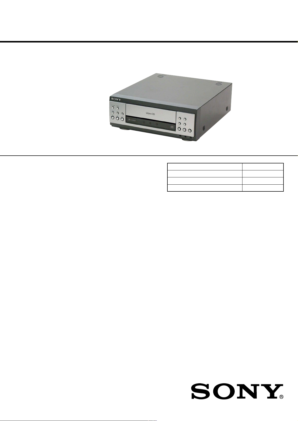
MCE-SV7
SERVICE MANUAL
Ver 1.0 2001.06
MCE-SV7 is the Video CD/CD play er
section in MHC-SV7AV.
E Model
Model Name Using Similar Mechanism NEW
CD Mechanism Type CDM63B
Base Unit Name BU-30BD61A
Optical Pick-up Name OP Assy (A-MAX.3)
SPECIFICATIONS
VIDEO CD/CD player section
System Compact disc and digital
Laser Semiconductor laser
Frequency response 2 Hz – 20 kHz (±0.5 dB)
Signal-to-noise ratio More than 90 dB
Dynamic range More than 90 dB
Video color system format
OPTICAL OUT
(Square optical connector jack, rear panel)
General
Dimensions (w/h/d)
Mass Approx. 2.8 kg
Design and specifications are subject to change
without notice.
audio system
(λ=795 nm)
Emission duration:
continuous
NTSC, PAL
Approx. 280 x 108 x 330 mm
9-873-155-01 Sony Corporation
2001F0500-1 Home Audio Company
C 2001.6 Shinagawa Tec Service Manual Production Group
VIDEO CD/CD PLAYER
MCE-SV7
NOTES ON HANDLING THE OPTICAL PICK-UP
BLOCK OR BASE UNIT
The laser diode in the optical pick-up block may suffer electrostatic break-down because of the potential difference generated
by the charged electrostatic load, etc. on clothing and the human
body.
During repair, pay attention to electrostatic break-down and also
use the procedure in the printed matter which is included in the
repair parts.
The flexible board is easily damaged and should be handled with
care.
NOTES ON LASER DIODE EMISSION CHECK
The laser beam on this model is concentrated so as to be focused
on the disc reflective surface by the objective lens in the optical
pick-up block. Therefore, when checking the laser diode emission, observe from more than 30 cm away from the objectiv e lens.
LASER DIODE AND FOCUS SEARCH OPERATION
CHECK
Carry out the “S curve check” in “CD section adjustment” and
check that the S curve waveforms is output three times.
Notes on chip component replacement
• Never reuse a disconnected chip component.
• Notice that the minus side of a tantalum capacitor may be dam-
aged by heat.
CAUTION
Use of controls or adjustments or performance of procedures
other than those specified herein may result in hazardous radiation exposure.
This appliance is classified as a CLASS 1 LASER product.
The CLASS 1 LASER PRODUCT MARKING is located on
the rear exterior.
Laser component in this product is capable of emitting radiation
exceeding the limit for Class 1.
The following caution label is located inside the unit.
Flexible Circuit Board Repairing
• Keep the temperature of the soldering iron around 270 ˚C during repairing.
• Do not touch the soldering iron on the same conductor of the
circuit board. (within 3 times)
• Be careful not to apply force on the conductor when soldering
or unsoldering.
SAFETY-RELATED COMPONENT WARNING!!
COMPONENTS IDENTIFIED BY MARK 0 OR DOTTED
LINE WITH MARK 0 ON THE SCHEMATIC DIA GRAMS
AND IN THE PARTS LIST ARE CRITICAL TO SAFE
OPERATION. REPLACE THESE COMPONENTS WITH
SONY PARTS WHOSE PART NUMBERS APPEAR AS
SHOWN IN THIS MANUAL OR IN SUPPLEMENTS PUBLISHED BY SONY.
2

TABLE OF CONTENTS
1. SERVICING NOTES ............................................... 4
2. GENERAL ................................................................... 5
3. DISASSEMBLY
3-1. Disassembly Flow ........................................................... 6
3-2. Cover ............................................................................... 7
3-3. CD Mechanism Deck (CDM63B) .................................. 7
3-4. MAIN Board ................................................................... 8
3-5. Front Panel Section......................................................... 8
3-6. PANEL Board, SUB PANEL Board ............................... 9
3-7. Lid (CD) .......................................................................... 9
4. TEST MODE.............................................................. 10
5. ELECTRICAL ADJUSTMENTS
CD Section ...................................................................... 11
VIDEO Section ............................................................... 11
6. DIAGRAMS
6-1. Block Diagram – CD SERVO Section – ....................... 12
6-2. Block Diagram – AUDIO/VIDEO Section – ................ 13
6-3. Block Diagram – MAIN Section – ................................ 14
6-4. Note For Printed Wiring Boards
and Schematic Diagrams ................................................ 15
6-5. Printed Wiring Board – BD Section – ........................... 16
6-6. Schematic Diagram – BD Section – .............................. 17
6-7. Printed Wiring Boards
– CD CHANGER Section –............................................ 18
6-8. Schematic Diagram – CD CHANGER Section – ......... 19
6-9. Printed Wiring Boards – AUDIO/VIDEO Section – ..... 20
6-10. Schematic Diagram
– AUDIO/VIDEO Section (1/3) – .................................. 21
6-11. Schematic Diagram
– AUDIO/VIDEO Section (2/3) – .................................. 22
6-12. Schematic Diagram
– AUDIO/VIDEO Section (3/3) – .................................. 23
6-13. Printed Wiring Boards – MAIN Section – .................... 24
6-14. Schematic Diagram – MAIN Section –......................... 25
6-15. Printed Wiring Boards – PANEL Section – .................. 26
6-16. Schematic Diagram – PANEL Section – ....................... 27
6-17. IC Pin Function Description ........................................... 32
MCE-SV7
7. EXPLODED VIEWS
7-1. Cover, Front Panel Section ............................................. 41
7-2. Chassis Section ............................................................... 42
7-3. CD Mechanism Deck Section-1 (CDM63B).................. 43
7-4. CD Mechanism Deck Section-2 (CDM63B).................. 44
7-5. Base Unit Section (BU-30BD61A) ................................ 45
8. ELECTRICAL PARTS LIST ............................... 46
3
MCE-SV7
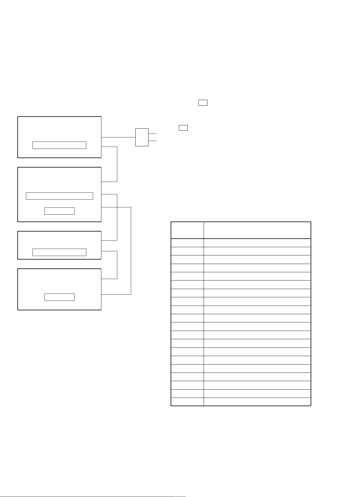
SECTION 1
SERVICING NOTES
This set is a component of the MHC-SV7AV.
The MHC-SV7AV system configuration is as shown below, and
therefore it does not operate normally unless all four components
are connected.
In performing the repair, connect all components with the system
cables.
Note: The precaution to the users is described on the label stuck
on the back panel (Video CD player) and in the troubleshooting
section in the Operation Manual.
System Configuration:
AC IN
TA
POWER SUPPLY
ST
MASTER & GRAPHIC µcon
DISPLAY
MCE
HTC & VMP µcon
TC
TC µcon
CD-TEXT TEST DISC
This unit is able to display the test data (character information)
written in the CD on its fluorescent indicator tube.
The CD-TEXT TEST DISC (TGCS-313:4-989-366-01) is used
for checking the display.
To check, perform the following procedure.
Checking Method:
1. Press the I/1 button to turn the power on, set the disc to the
disc table with the “test disc” label facing up, and chuck the
disc.
2. Press the [CD] button to set CD function, and press the
N button to playback the disc.
3. The following will be displayed on the liquid crystal display.
Display : 1KHZ/0DB/L R
4. Pressing the [-- ] or [ +] button, select the track. The text
data of each track will be displayed.
For details of the displayed contents for each track, refer to “Table
1 : CD-TEXT TEST DISC TEXT Data Contents”.
Restrictions in CD-TEXT Display
In this unit, some special characters will not be displayed properly. These will be displayed as a space or a character resembling
it.
Table 1 : CD-TEXT TEST DISC TEXT Data Contents
(TRACKS No. 1 to 20:Normal Characters)
TRACK
No.
1 1kHz/0dB/L&R
2 20Hz/0dB/L&R
3 40Hz/0dB/L&R
4 100Hz/0dB/L&R
5 200Hz/0dB/L&R
6 500Hz/0dB/L&R
7 1kHz/0dB/L&R
8 5kHz/0dB/L&R
9 7kHz/0dB/L&R
10 10kHz/0dB/L&R
11 16kHz/0dB/L&R
12 18kHz/0dB/L&R
13 20kHz/0dB/L&R
14 1kHz/0dB/L&R
15 1kHz/–1dB/L&R
16 1kHz/–3dB/L&R
17 1kHz/–6dB/L&R
18 1kHz/–10dB/L&R
19 1kHz/–20dB/L&R
20 1kHz/–60dB/L&R
Note: Track No. 21 to 99 are not displayed.
.>
Displayed Contents
4
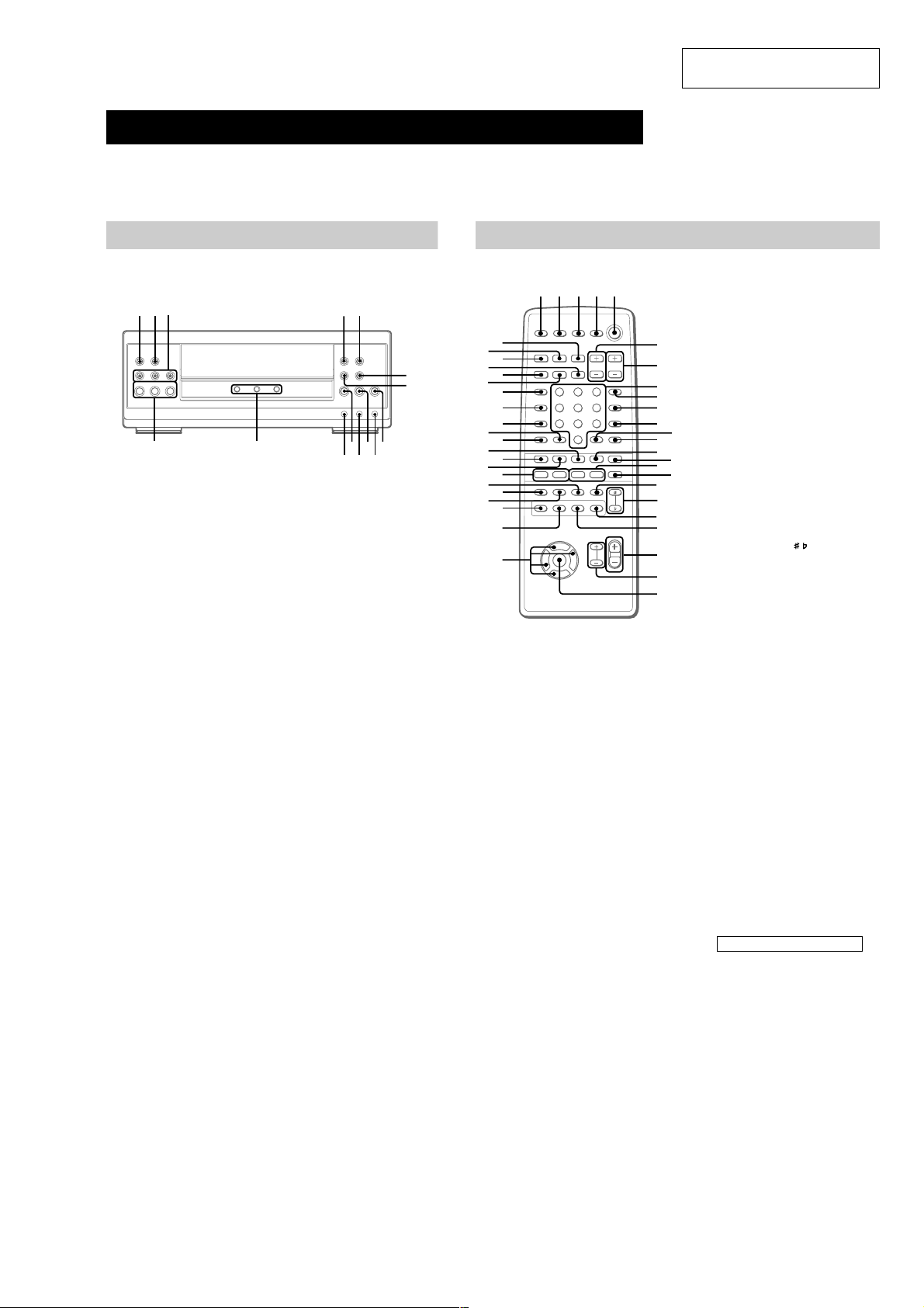
Parts Identification
The items are arranged in alphabetical order.
Refer to the pages indicated in parentheses ( ) for details.
SECTION 2
GENERAL
MCE-SV7
This section is extracted from
instruction manual.
Main unit
VIDEO CD/CD player
wk wle; ea
1 2 3
rs
DISC 1–3 rs (14, 16, 17, 25)
DISC 1–3 indicators ra
DISC 1–3 Z (eject) e; (14–16)
NEXT ek (14, 15)
PLAY MODE wk (14, 16, 17, 25)
PREV r; (14, 15)
REPEAT wl (15, 16)
RETURN O eh (15)
N SELECT (play) el (14–17,
19, 21, 34)
X (pause) ej (14, 16)
x (stop) eg (14–16, 19, 21, 24,
34)
. (go back) ef (14–17, 21,
25)
> (go forward) ed (14–17, 21,
25)
m (rewind) ea (14, 16)
M (fast forward) es (14, 16)
es
mM
.
>
HS x
ehekr;
Remote Control
1234 5
rg
rf
rd
ed
ef
rs
r;
ra
el
ek
ej
eh
egejelra
ef
es
e;
wk
eg
ed
ea
wl
wj
O
nNnN
Mm>.
wh
V
wg
Bb
v
6
7
8
9
q;
qa
qs
qd
qf
x
X
qh
qk
qg
qj
ql
w;
wa
ws
wd
wf
CHECK qd (17)
CLEAR qs (17, 19)
CLOCK/TIMER SELECT 3
(26, 35)
CLOCK/TIMER SET 2 (13, 25,
34)
DBFB ej (27)
DIGITAL r; (36, 40)
DISPLAY rd (13, 18, 33, 40)
D.SKIP 9 (14, 16, 20, 21)
ENTER wf (11, 13, 15, 17, 21,
22, 25, 26, 30–33, 35)
EQ wh (31)
EQ ON/OFF wa (32)
FILE SELECT +/– wd (27, 28,
32)
FUNCTION el (10, 14–17, 24,
25, 34, 36)
GROOVE ek (27)
KARAOKE PON qk (33)
KEY CONTROL / ql (33)
MD rs (36)
Numeric buttons 8 (15, 16, 19,
20, 21)
ON SCREEN wk (18)
PICTURE EFFECT wl (21)
PRESET –/+, PREV/NEXT ea
(14, 15, 20, 22)
REPEAT q; (15, 16)
RETURN O eg (15)
PLAY MODE qa (14, 16, 17, 25)
SELECT CD N es (14–17, 19,
21)
SET UP w; (11, 13, 30, 32, 33)
SLEEP 1 (34)
SPECIAL MENU e; (19, 20, 21)
SPECTRUM ANALYZER rf
(33)
SUR wj (30)
TAPE A nN ef (23)
TAPE B nN qf (23, 24)
TUNER/BAND ed (22)
TUNING –/+ qh (22)
TV CH +/– 7 (10)
TV VOL +/– 6 (10)
TV @/1 4 (10)
TV/VIDEO rg (10)
VIDEO ra (36)
VOL +/– ws
BUTTON DESCRIPTIONS
@/1 (power) 5
X (pause) qj
x (stop) qg
./> (go back/go forward)
ea
m/M (rewind/fast forward)
qh
O/o/P/p wg
>10 eh
5
MCE-SV7
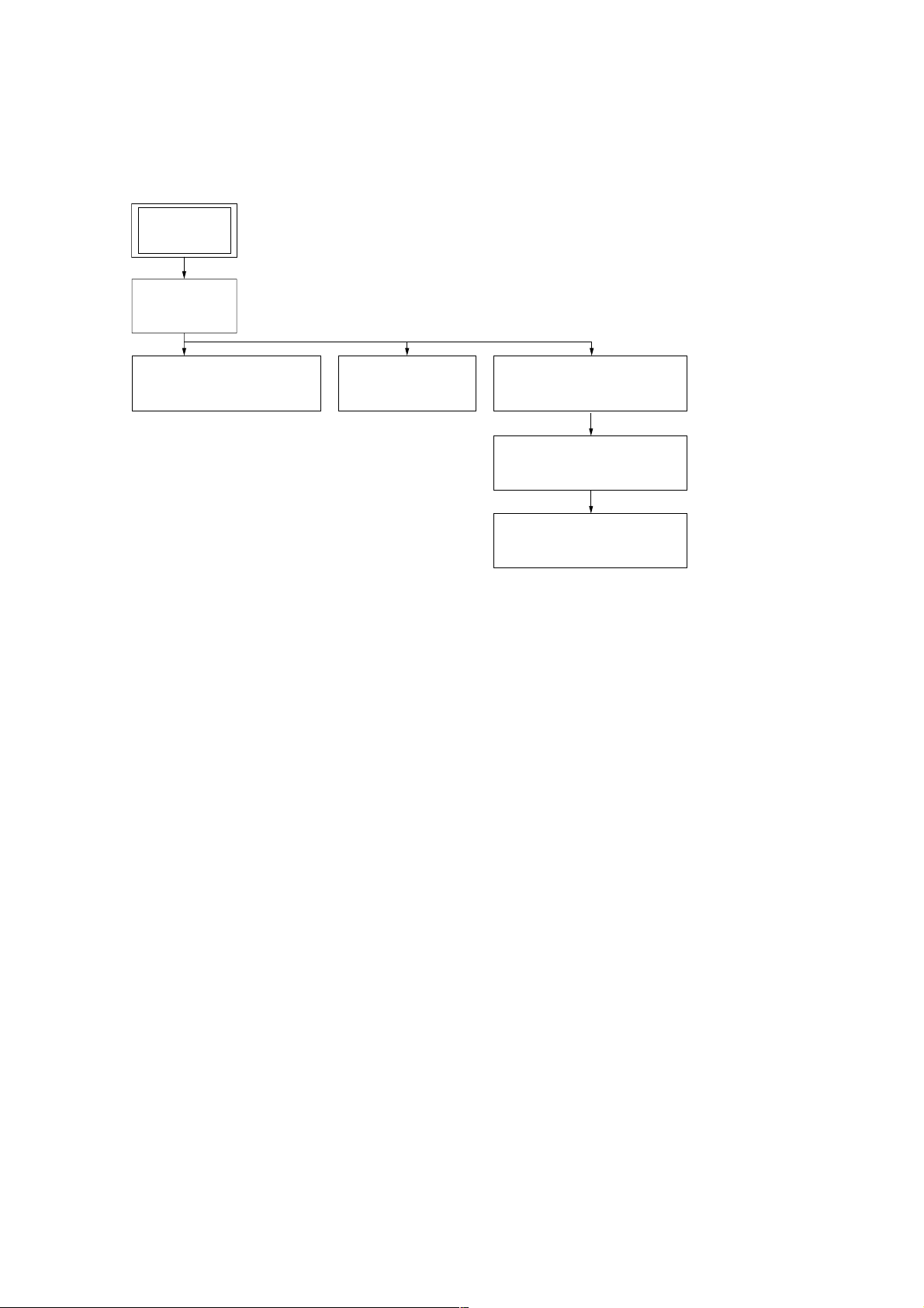
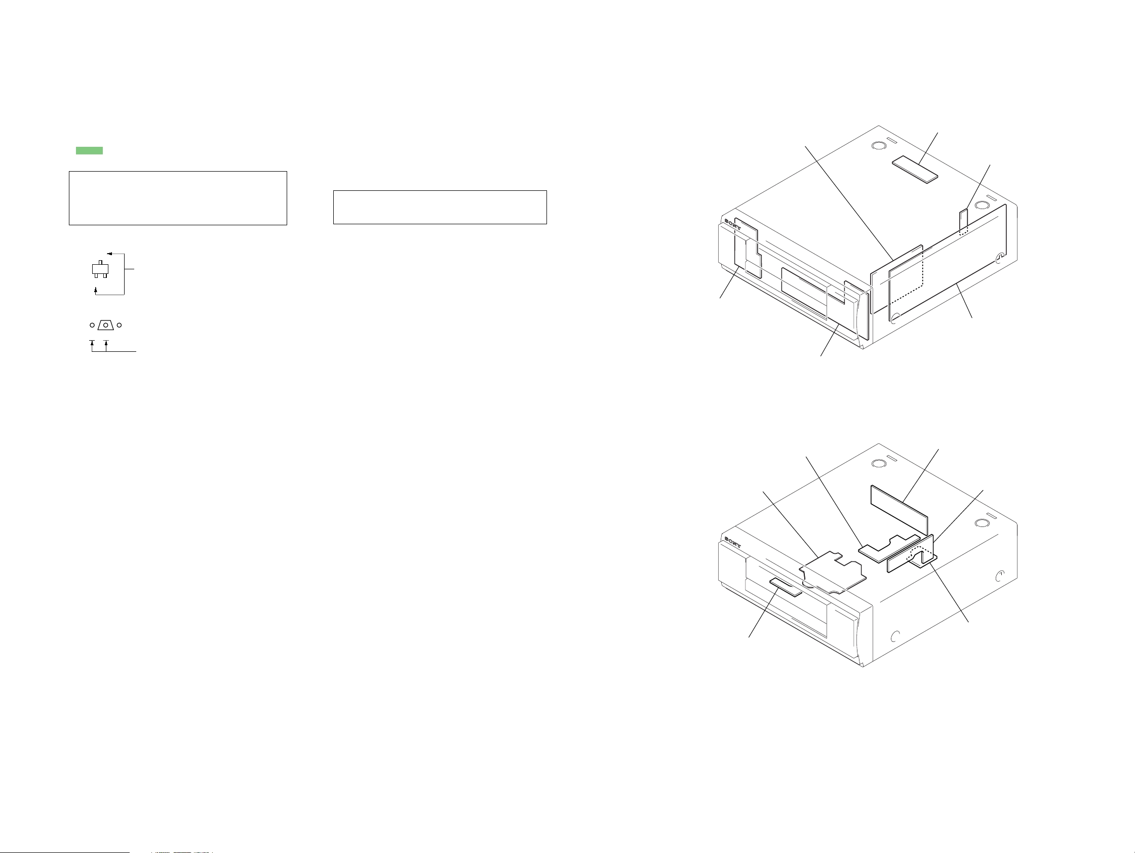
• This set can be disassembled in the order shown below.
3-1. DISASSEMBLY FLOW
SET
3-2. COVER
(Page 7)
SECTION 3
DISASSEMBLY
3-3. CD MECHANISM DECK
(CDM63B)
(Page 7)
3-4. MAIN BOARD
(Page 8)
3-5. FRONT PANEL SECTION
(Page 8)
3-6. PANEL BOARD,
SUB PANEL BOARD
(Page 9)
3-7. LID (CD)
(Page 9)
6
Note: Follow the disassembly procedure in the numerical order given.
)
r
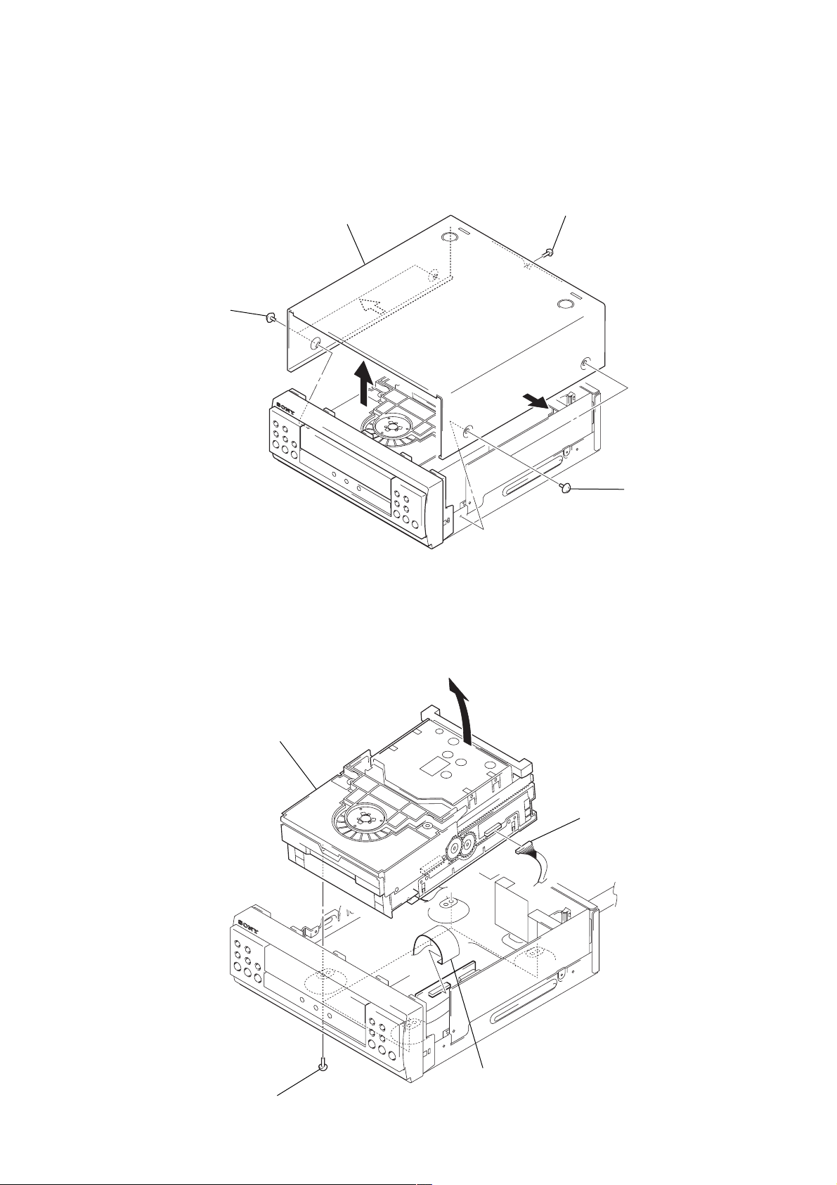
3-2. COVER
3
cover
1
two screws
(case 3 TP2)
2
screw
(BVTT3 × 6)
MCE-SV7
3-3. CD MECHANISM DECK (CDM63B)
4
CD mechanism deck (CDM63B)
1
two screws
(case 3 TP2
2
connecto
(CN701)
3
four screws
(BVTP3
1
wire (flat type) (25 core)
(CN501)
×
8)
7
MCE-SV7
)
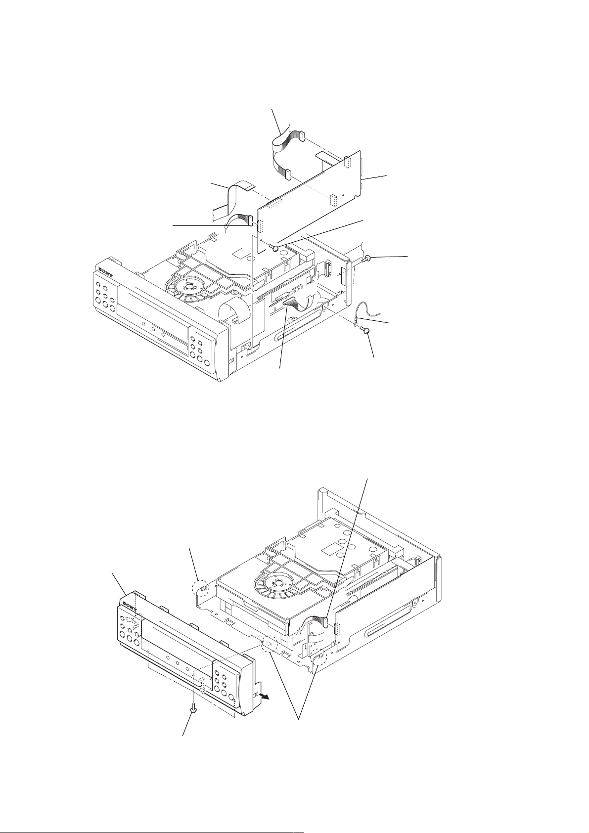
3-4. MAIN BOARD
1
wire (flat type) (13 core)
(CN301)
2
connector
(CN401)
2
two connectors
(CN101, 102)
5
3
screw
(BVTP3 × 8)
MAIN board
3
two screws
(BVTP3 × 8
3-5. FRONT PANEL SECTION
3
4
front panel section
claw
2
connector
(CN701)
3
1
connector
(CN401)
4
lug
screw
(BVTP3 × 8)
3
two claws
2
three screws
(BVTP3
×
8)
8
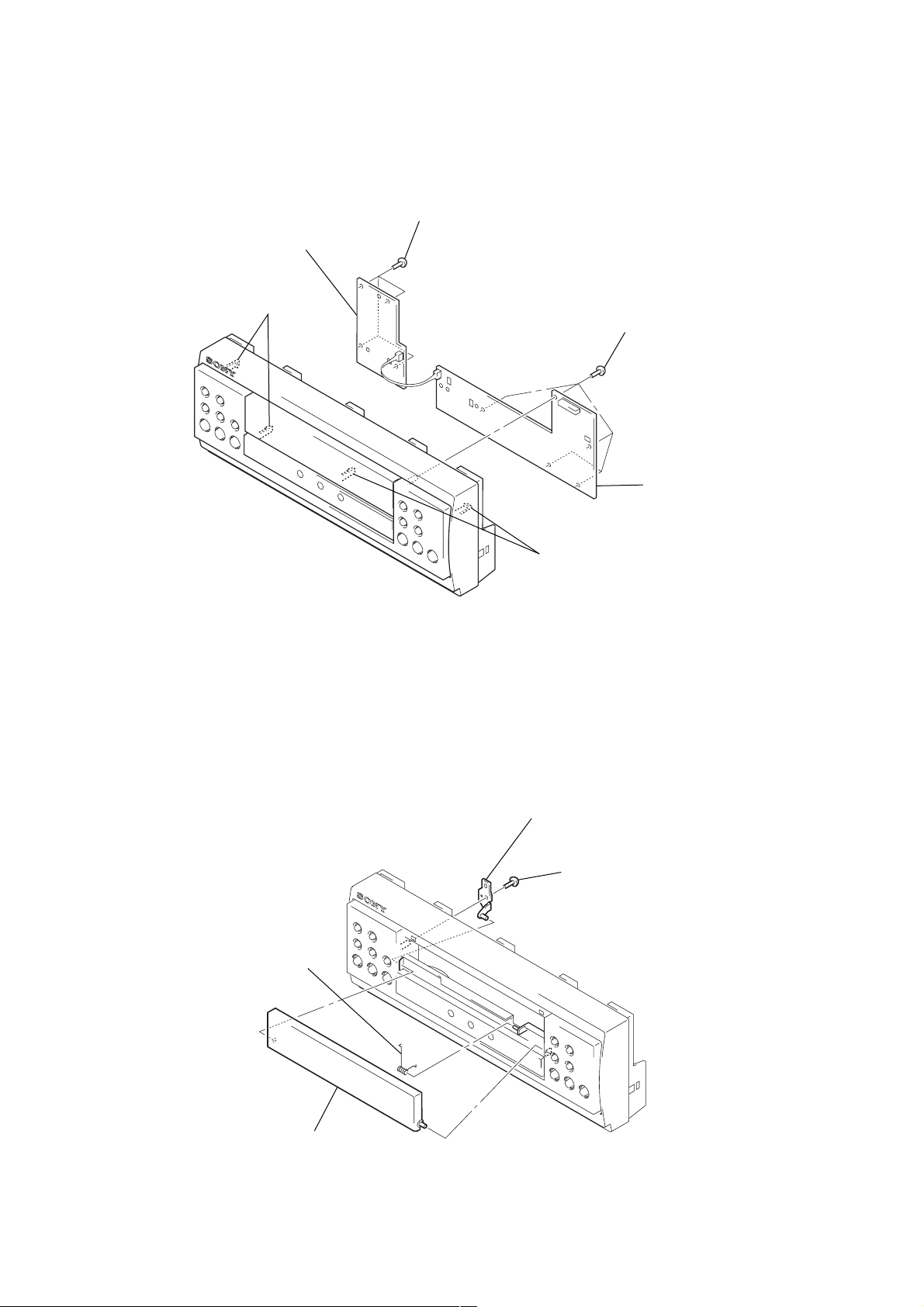
3-6. PANEL BOARD, SUB PANEL BOARD
d
)
4
6
SUB PANEL board
5
two claws
four screws
(BVTP2.6
MCE-SV7
×
8)
1
five screws
(BVTP2.6
3
×
8)
PANEL boar
3-7. LID (CD)
4
spring (CD)
2
two claws
2
bracket (LID) assy
1
screw
(BVTP2.6 × 8
3
lid (CD)
9

MCE-SV7
SECTION 4
TEST MODE
Note: Use following buttons in the test mode.
no mark: Button of video CD unit (MCE-SV7)
*1 : Button of amplifier unit (TA-SV7AV)
*2 : Button of tuner unit (ST-SV7)
[CD Delivery Mode]
• This mode moves the optical pick-up to the position durable to
vibration. Use this mode when returning the set to the customer
after repair.
Procedure:
1. Press the I/1 *1 button to turn the power on.
2. Turn the [FILE SELECT] *1 knob to set the CD function.
3. While pressing the [EQ ON/OFF] *1 button, press the I/1 *
button.
4. The message “LOCK” is displayed on the fluorescent indica-
tor tube of tuner unit and turn the power off automatically , and
the CD delivery mode is set.
[GC Test Mode]
Enter the GC Test Mode
Procedure 1:
1. Press the I/1 *1 button to turn the power on.
2. While pressing the both [PLAY MODE] and [ ] buttons, press
Z
the [ ] (DISC 1) button.
x
3. LEDs and fluorescent indicator tube are all turned on of all
units.
Procedure 2:
1. Press the I/1 *1 button to turn the power on.
2. While pressing the both [STEREO/MONO] *2 and
[CINEMA STUDIO C] *
1
buttons, press the [CLOCK/TIMER]
*2 button.
3. LEDs and fluorescent indicator tube are all turned on of all
units.
[CD Service Mode]
• This mode can run the CD sled motor optionally. Use this mode,
for instance, when cleaning the optical pick-up.
Procedure:
1. Press the I/1 *1 button to turn the power on.
2. Turn the [FILE SELECT] *1 knob to set the CD function.
3. While pressing the both [PLAY MODE] and [ ] buttons, press
.
the [ ] button.
x
4. Set to the CD service mode.
5. With the CD in stop status, press the [ ] button to move the
M
optical pick-up to outside track, or press the [ ] button to
1
inside track.
6. To release from this mode, perform as follows.
1) Move the optical pick-up to the most inside track.
2) Disconnect the power cord.
Notes: • Always move the optical pick-up to most inside track when
releasing from this mode. Otherwise, a disc will not be unloaded.
• Do not run the sled motor excessively, otherwise the gear can
be chipped.
[CD Cancellation Mode of Repeat Limitation]
• This mode can cancel the CD repeat limitation (5 times).
Procedure:
1. Press the I/1 *1 button to turn the power on.
2. Turn the [FILE SELECT] *1 knob to set the CD function.
3. While pressing the both [PLAY MODE] and [ ] buttons, press
x
the [REPEAT] button.
4. CD repeat limitation is canceled.
5. To release this mode, disconnect the power cord.
m
Version Display Mode
Procedure:
1. Enter the GC test mode.
2. Each time the
[DISC 1] or [TUNER MEMORY] *
2
button is
pressed, microcomputer or mechanism deck version is displayed of each unit.
3. Press the [DISC 3] or [TUNING +] *2 button to detail is displayed the version.
Key Check Mode
Procedure:
1. Enter the GC test mode.
2. Press the [DISC 2] or [TUNING --] *2 button to set the key
check mode, and displays “K 0 J 0 V 0” on the fluorescent
indicator tube of tuner unit.
3. All buttons are pressed of video CD unit, all LEDs are blinking of video CD unit. (not change the display of fluorescent
indicator tube)
Releasing the GC Test Mode
T o release from this mode, press three buttons in the same manner
as entering this mode or disconnect the power cord.
10
SECTION 5
r
)
TP (DVC)
TP (FEO)
TP (XPCK)
TP (TEO)
TP (RFDC)
TP (VC)
TP
(RFAC)
IC103
IC101
TP (FEI)
R120
r
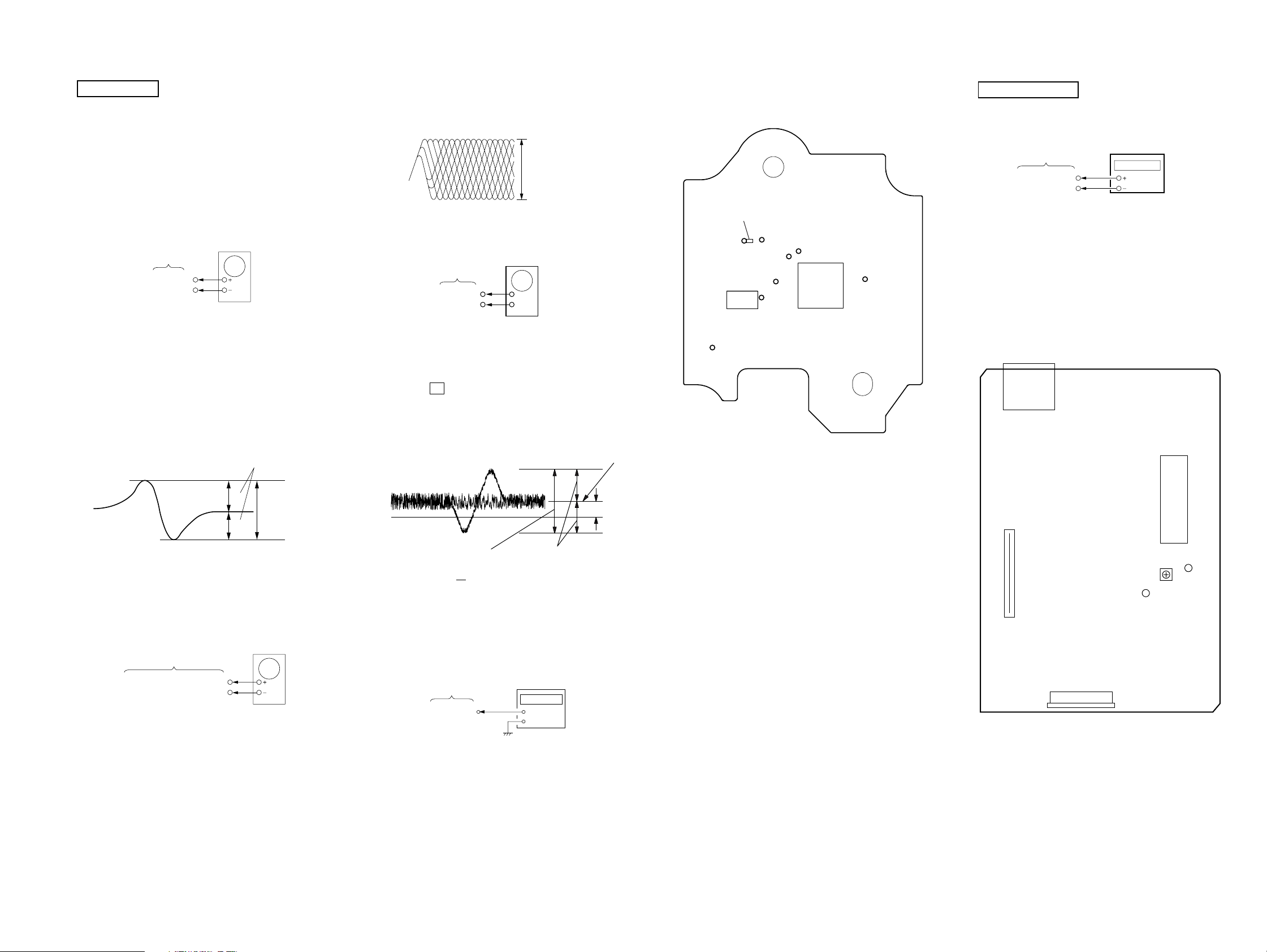
ELECTRICAL ADJUSTMENTS
MCE-SV7
CD SECTION
Note :
1. CD Block is basically designed to operate without adjustment.
Therefore, check each item in order given.
2. Use YEDS-18 disc (3-702-101-01) unless otherwise indicated .
3. Use an oscilloscope with more than 10MΩ impedance.
4. Clean the object lens by an applicator with neutral detergent
when the signal level is low than specified value with the
following checks.
S-Curve Check
Oscilloscope
BD board
TP(FEO)
TP(DVC)
Procedure :
1. Connect an oscilloscope to TP (FEO) and TP (DVC).
2. Connect between TP (FEI) and TP (VC) by lead wire.
3. Turn Power switch on.
4. Load the disc (YEDS-18) and actuate the focus search. (In
consequence of open and close the disc tray, actuate the focus
search)
5. Confirm that the oscilloscope waveform (S-curve) is
symmetrical between A and B. And confirm peak to peak level
within 4 ±1 Vp-p.
S-curve waveform
symmetry
Note: Clear RF signal wav eform means that the shape “◊” can be
clearly distinguished at the center of the waveform.
RF signal waveform
VOLT/DIV : 200mV
TIME/DIV : 500ns
level : 1.1 ± 0.3Vp-p
E-F Balance (1 Track jump) Check
oscilloscope
BD board
TP (TEO)
TP (DVC)
+
–
Procedure:
1. Connect an oscilloscope to TP (TEO) and TP (DVC).
2. Turn Power switch on.
3. Load the disc (YEDS-18) and playback the number five track.
4. Press the X button. (Becomes the 1track jump mode.)
5. Confirm that the level B and A (DC v oltage) on the oscilloscope
waveform.
1 track jump waveform
Center of
waveform
Checking Location :
[ BD BOARD ] — SIDE B —
VIDEO SECTION
Video Frequency Adjustment
Connection:
frequency counte
VMP board
TP (27MHz)
TP (GND)
Procedure:
1. Connect a frequency counter to TP (27MHz) and TP (GND).
2. Turn power switch on.
3. Turn the [FUNCTION] knob of amplifier unit (TA-SV7AV) to
set the CD function.
4. Adjust CT503 on the VMP board so that the frequency counter
reading 27.0 MHz ± 80 Hz at stop status.
Adjustment Location:
[VMP BOARD] (SIDE A)
J301
IC507
A
within 4 ±1Vp-p
B
7. After check, remove the lead wire connected in step 2.
Note : • Try to measure several times to make sure than the ratio
of A : B or B : A is more than 10 : 7.
• Take sweep time as long as possible and light up the
brightness to obtain best waveform.
RF Level Check
oscilloscope
BD board
TP (RFAC) or TP(RFDC)
TP(DVC)
Procedure :
1. Connect an oscilloscope to TP (RFAC) and TP (DVC).
2. Turn Power switch on.
3. Load the disc (YEDS-18) and playback.
4. Confirm that the oscilloscope waveform is clear and check RF
5. Measure the RFDC in the same way.
signal level is correct or not.
B
0V
level=1.3 ±0.6Vp-p
Specification level: x 100=less than ±22%
A
B
Symmetry
A (DC voltage
6. After check, remove the lead wire connected in step 1.
RF PLL Free-run Frequency Check
Procedure :
1. Connect a frequency counter to TP (XPCK) and GND.
BD board
TP (XPCK)
frequency counte
+
–
2. Turn Power switch on.
3. Load the disc (YEDS-18) and playback the number five track.
4. Confirm that the reading on frequency counter is 4.3218MHz.
CN501
CN502
TP (27MHz)
TP (GND)
CT503
Video
Frequency
Adjustment
1111
MCE-SV7
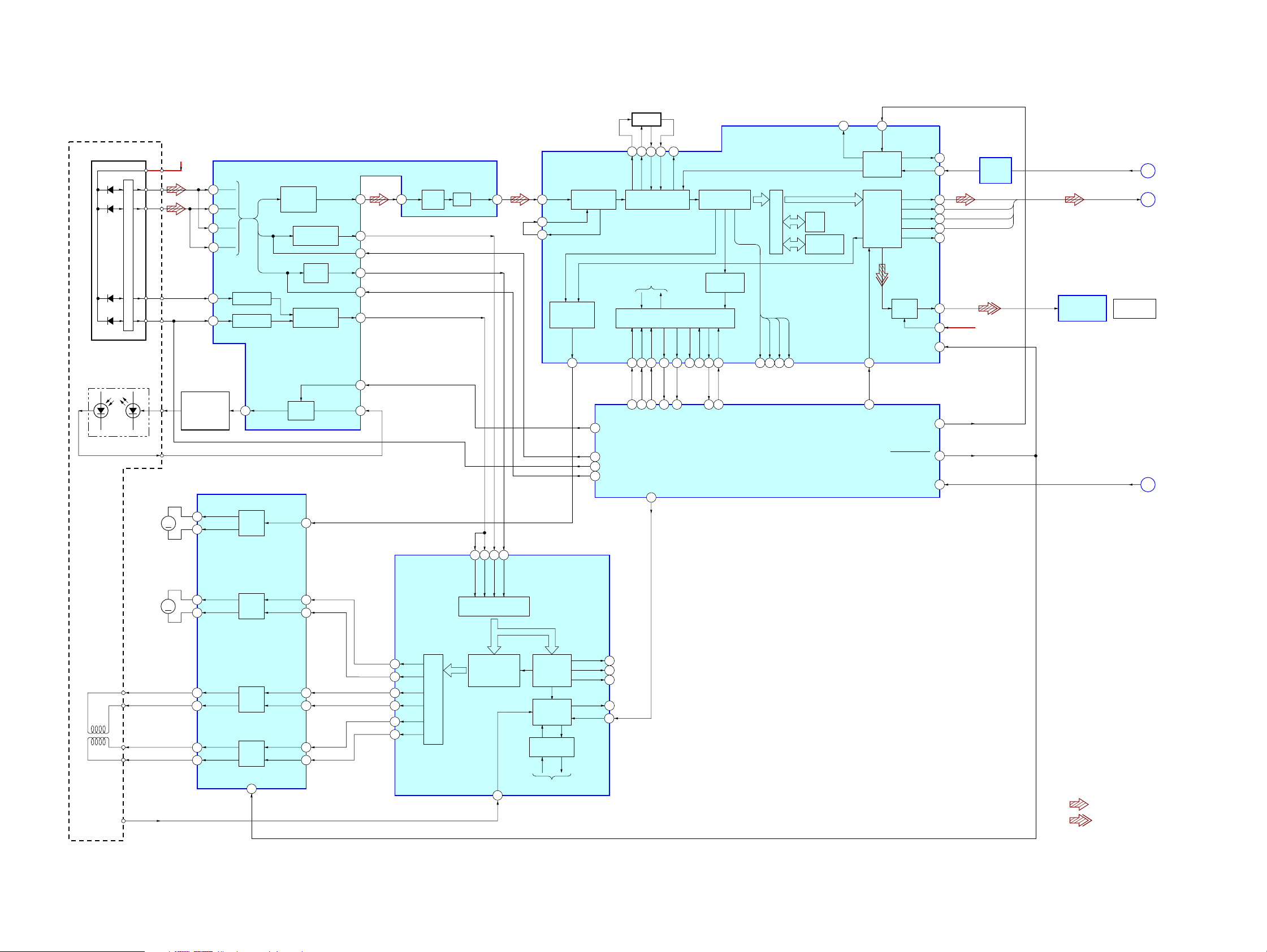
6-1. BLOCK DIAGRAM – CD SERVO Section –
SECTION 6
DIAGRAMS
DETECTOR
A
B
F
E
OPTICAL PICK-UP
BLOCK
(A-MAX. 3)
LASER DIODE
PD
I-V AMP
LD
M101
(SPINDLE)
M
CD +5V
A
6
B
7
C
8
D
9
F
11
F I-V AMP
E
10
E I-V AMP
AUTOMATIC
POWER
CONTROL
Q101
FOCUS/TRACKING COIL DRIVE,
VO4+
5
VO4–
10
1
SPINDLE/SLED MOTOR DRIVE
IC102
MOTOR
DRIVE
FILTER
RF AMP,
FOCUS/TRACKING ERROR AMP
RF
SUMMING
AMP
FOCUS
ERROR AMP
RF DC
AMP
TRACKING
ERROR AMP
LD
IN4R
APC LD
AMP
24
AC
SUM
RFDCO
RFDCI
SW
IC103
EQ
IN
4
FE
16
FEI
17
28
29
TE
18
12
PD
2
RFAC
3
VCA
RFAC
EQ
15
DIGITAL SIGNAL PROCESSOR
IC101 (1/2)
RFAC
50
49
48
ASYMMETRY
CORRECTOR
ASYI
ASYO
DIGITAL
CLV
PROCESSOR
MDP
25 76 77
LD ON
82
PWM1
28
PWM2
26
PWM3
24
53 55
FILO
TO SERVO AUTO
SEQUENCER
DATA
95 5 97 1 18 84 83 10
DSP DATA
FILI
PCO
CLTV
DIGITAL PLL
CPU INTERFACE
SENS
CLOK
XLAT
DSP CLK
DSP LATCH
SENSE CLK
2
125254
XPCK
EFM
DEMODULATOR
INTERNAL BUS
SUBCODE
PROCESSOR
SQCK
SQSO
EXCK
SCOR
SBSO
79 801574 6 5 10 111368 3
SCOR
SENSE
SUBQ CLK
SUBQ DATA
WFCK
XUGF
GFS
EMPH
VIDEO CD CONTROLLER
IC502 (1/2)
32K
RAM
ERROR
CORRECTOR
16 69
C4M
CLOCK
GENERATOR
DIGITAL
INTERFACE
MUTING
DSP MUTING
XTSL
D/A
DIGITAL
DEVICE RESET
OUT
XTAO
XTAI
PCMD
BCK
LRCK
C2PO
WDCK
DOUT
MD2
XRST
CTRL1
XRESET
72
71
66
67
65
14
17
64
63
2
11
77
12
OSC
BUFFER
IC106
DATA
BCK
LRCK
C2PO
CD +3.3V
OPTICAL
TRANSCEIVER
IC102
MCLK
33.8MHz
DATA, BCK,
LRCK, C2PO
OPTICAL OUT
TO ST-SV7
M-RESET
A
B
C
(Page 13)
(Page 13)
(Page 14)
2-AXIS
DEVICE
(TRACKING)
(FOCUS)
LIMIT
SWITCH
M102
(SLED)
40 41 39 43
DIGITAL SERVO
PROCESSOR
IC101 (2/2)
VO3+
1
M
2
55
56
47
52
VO3–
VO2+
VO2–
VO1+
VO1–
MOTOR
DRIVE
COIL
DRIVE
COIL
DRIVE
STBY
8
IN3+
IN3–
IN2+
IN2–
IN1+
IN1–
27
26
SFDR
29
SRDR
30
32
31
35
34
TFDR
31
TRDR
32
FFDR
33
FRDR
34
PWM GENERATOR
FOCUS/TRACKING/SLED
FE
TE
SE
RFDC
A/D
CONVERTER
FOCUS/
TRACKING/SLED
SERVO DSP
SSTP
26
MIRR,
DFCT, FOK
DETECTOR
SERVO
INTERFACE
SERVO AUTO
SEQUENCER
TO CPU INTERFACE
FOK
MIRR
DFCT
COUT
SCLK
22
20
21
19
8
• SIGNAL PATH
: CD PLAY (ANALOG OUT)
: CD PLAY (DIGITAL OUT)
1212
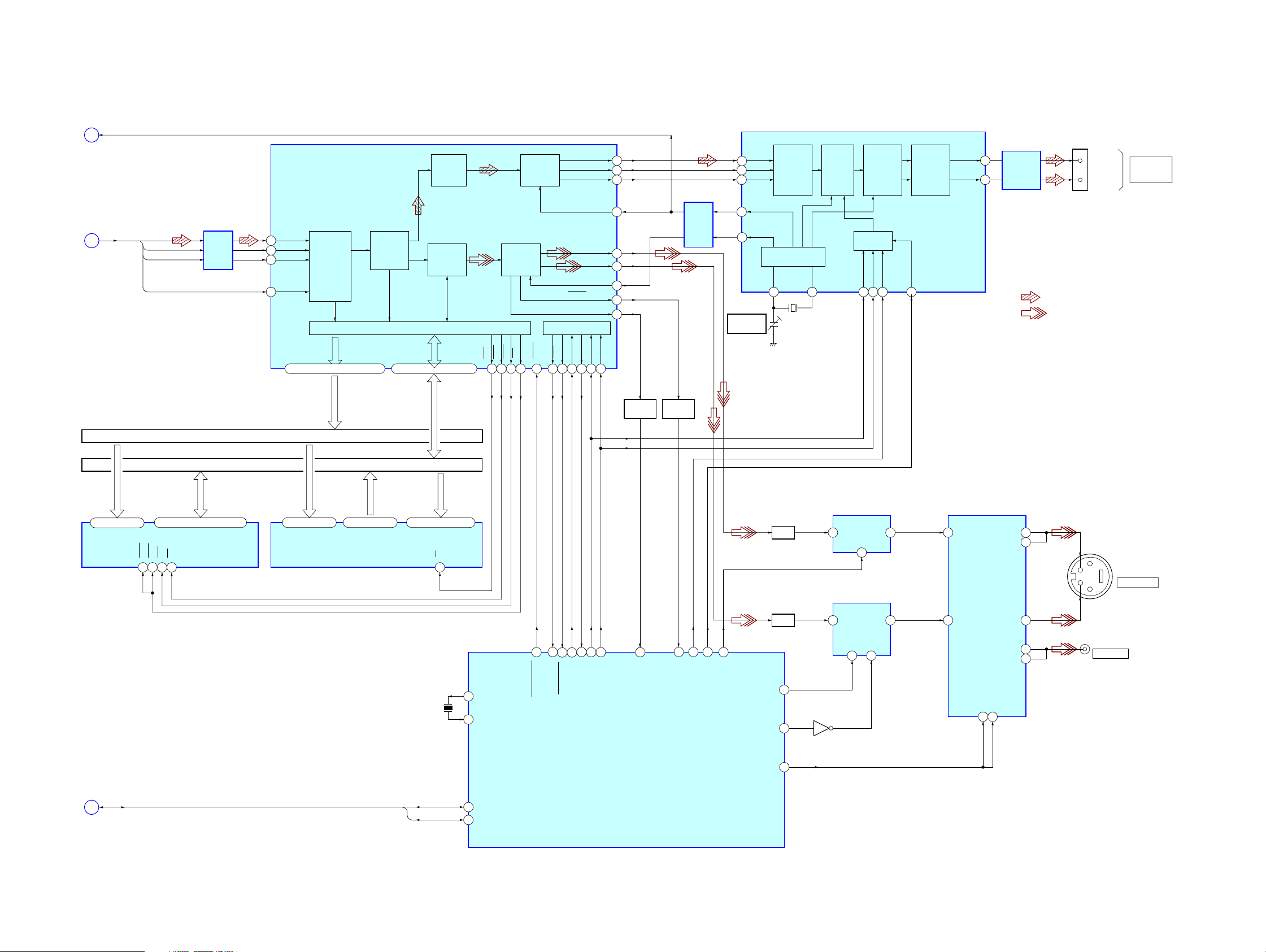
6-2. BLOCK DIAGRAM – AUDIO/VIDEO Section –
MCLK 33.8MHz
A
(Page 12)
MPEG VIDEO/AUDIO DECODER,
VIDEO SIGNAL PROCESSOR
IC505
MPEG
AUDIO
DECODER
AUDIO
INTERFACE
CIRCUIT
DA-DATA
DA-BCK
DA-LRCK
MCE-SV7
DIGITAL FILTER,
D/A CONVERTER
IC509
CN102 (1/2)
110
111
108
DATA
18
17
19
BCK
LRCK
INPUT
INTERFACE
CIRCUIT
DIGITAL
FILTER,
NOISE
SHAPER
CIRCUIT
D/A
CONVERTER
LOW-PASS
FILER
VOUTL
VOUTR
14
LOW-PASS
FILER
IC101
11
1
3
VCD L-IN
VCD R-IN
SYSTEM
CONTROL 3
TO ST-SV7
B
(Page 12)
16 – 19, 22 – 26
D-RAM
IC507
DATA, BCK,
LRCK, C2PO
A0 – A8
A0 – A8
UCAS
DATA
BCK
LRCK
C2PO
LCAS
DA-XCLK
86
CD-DATA
LEVEL
SHIFT
IC501
D0 – D15
DQ1 – DQ16
RAS
WE
14 132928
4
CD-BCK
3
CD-LRCK
5
CD-C2PO
6
MA0 – MA10
ADDRESS BUS
DATA BUS
12 – 5, 27, 26, 23
PROGRAM ROM
CD-ROM
INTERFACE
CIRCUIT
58 – 56, 54, 52 – 50, 48, 46 – 44 10 – 15, 17, 19, 21, 23 – 29
A0 – A10
A0 – A10
A0 – A10
IC510
13 – 15, 17 – 212 – 5, 7 – 10, 31 – 34, 36 – 39
MPEG
SYSTEM
DECODER
D-RAM/ROM INTERFACE
MD0 – MD15
D0 – D7
O0 – O7
MPEG
VIDEO
DECODER
D0 – D15
D8 – D14
25, 4, 28, 29, 3, 2, 30
A11 – A17
CE
22
PROCESS
CIRCUIT
RAS0
MWE
MCE
37
38 42 40 60
VIDEO
CAS
CPU INTERFACE
HRDY
HINT
RESET
113
114 121
Y-OUT
C-OUT
VCK-IN
VSYNC/CSYNC
HSYNC
HSEL
HD-OUT
HD-IN
112
119
117
HCK
DATA
CLK
69
75
106
93
101
BUFFER
Q501
BUFFER
Q502
OSC
BUFFER
IC504
384FSO
20
MCKO
4
CT503
VIDEO
FREQUENCY
TIMING CONTROL/
CLOCK GENERATOR
XT2
B.P.F.
X503
27MHz
XT1
MODE
CONTROL
ML
MC
MD
9 724 1
8
RSTB
10
• SIGNAL PATH
: CD PLAY (AUDIO)
: CD PLAY (VIDEO)
2
Y IN
Y/C DECODER
IC304
Y OUT1
Y OUT2
15
14
2
4
3
1
J801
S VIDEO OUT
Y AMP
IC303
10
VIN
CONT
C AMP
IC302
1
VOUT
5
D
(Page 14)
IIC-DATA,
IIC-CLK
X501
10MHz
IIC-DATA
IIC-CLK
13
15
30
29
XOUT
XIN
I2C_DATA
I2C_CLK
85
86
CL680 HINT
CL680 HRDY
CL680 RESET
VIDEO CD CONTROLLER
36
8720
DATAI
CL680 SEL
IC502 (2/2)
3735
CLK1
DATAO
21
H. SYNC IN
45
VSYNC
1313
88
DF LATCH
66
DAC RESET
3
RESOLUTION
V. MUTING
CHOMA
LEVEL
BGP
B.P.F.
22
65
1
VIN
TINT5BGP
8
4
Q301
VOUT
6
7
C IN
MIX OUT1
MIX OUT2
MUTE A8MUTE B
1
C OUT
9
12
11
J802
VIDEO OUT
MCE-SV7
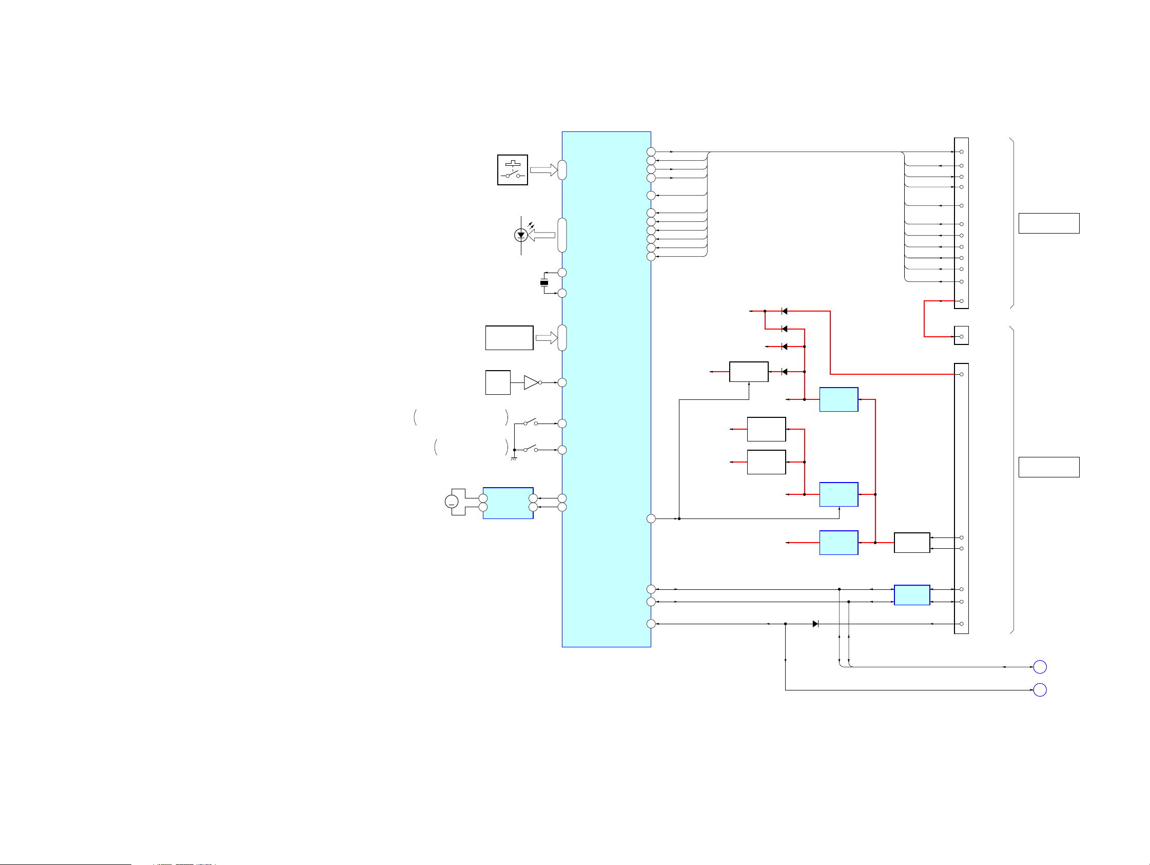
6-3. BLOCK DIAGRAM – MAIN Section –
SYSTEM CONTROLLER
IC401
S701 – 708,
D701 – 705
SUB TRAY1 – 3
HEIGHT SENSOR
DISC IN
DETECT
IC751
ON: WHEN SUB TRAY SLIDES OUT
OF THE CHUCKING POSITION
ON: WHEN SUB TRAY IS
CHUCKING POSITION
LOADING MOTOR DRIVE
OUT1
M721
(LOADING)
MM
4
2
OUT2
S711 – 720
IC731 – 733
IC701
X401
16MHz
S741
S742
(OUT)
FIN
RIN
Q701
(IN)
97, 95
KEY0, KEY1T-SENS1 – TSENS3
LED_DISC1
LED_DISC2
LED_DISC3
LED_PLAY
65 – 83, 88
LED_PAUSE
13
X-OUT
15
X-IN
48 – 50
52
DISC-SENS
47
CLOSE
46
OPEN
45
7
9
44
LOAD-OUT
LOAD-IN
EXP-OUT DATA
EXP-IN DATA
EXP-CLK
EXP-LAT
KEY2 (TC)
A-TRIG
B-TRIG
R/PB/PASS
A-SHUT
B-SHUT
B-HALF
CD POWER
CN103
DATA-OUT
85
84
87
86
94
55
53
59
89
90
91
38
DATA-IN
CLK
LAT
KEY2
ATRIG
BTRIG
REC/PB/PAS
ASHUT
BSHUT
BHALF
A+5V (SW)
VIDEO +3.3V
CD +3.3V
EVER+5V
B+ SWITCH
Q501, 502
D+5V
OPT B+
+3.3V
REGULATOR
Q531
+3.3V
REGULATOR
Q301
D+5V (SW)
M+7V
D512
D513
D514
D511
+5.7V
REGULATOR
IC502
+5V
REGULATOR
IC501
+7V
REGULATOR
IC503
DATA-OUT
DATA-IN
CLK
LAT
KEY2
ATRIG
BTRIG
REC/PB/PAS
ASHUT
BSHUT
BHALF
RECT
D501 – 504
10
9
8
7
6
4
5
11
12
13
14
3
CN102 (2/2)
7
CN101
5
8
9
DATA-OUT
DATA-IN
CLK
LAT
KEY2
ATRIG
BTRIG
REC/PB/PAS
ASHUT
BSHUT
BHALF
UNREG
UNREG (TC)
EVER +5V
AC
AC
SYSTEM CONTROL 5
FROM TC-S3
SYSTEM CONTROL 3
TO ST-SV7
IIC-DATA
IIC-CLK
RESET
30
29
12
D105
IIC-DATA
IIC-CLK
BUFFER
IC504
2
1
4
MRESET
IIC-DATA,
IIC-CLK
M-RESET
D
C
(Page 13)
(Page 12)
1414
MCE-SV7
d
6-4. NOTE FOR PRINTED WIRING BOARDS AND SCHEMATIC DIAGRAMS
(In addition to this, the necessary note is printed in each block)
Note on Printed Wiring Boards:
• X : parts extracted from the component side.
• Y : parts extracted from the conductor side.
f
•
•
(The other layers' patterns are not indicated.)
Caution:
Pattern face side: Parts on the pattern face side seen from
(Side B) the pattern face are indicated.
Parts face side: Parts on the parts face side seen from
(Side A) the parts face are indicated.
• Indication of transistor.
: internal component.
: Pattern from the side which enables seeing.
C
B
B
Q
E
Q
CE
These are omitted.
These are omitted.
Note on Schematic Diagram:
• All capacitors are in µF unless otherwise noted. pF: µµF
50 WV or less are not indicated except for electrolytics
and tantalums.
• All resistors are in Ω and 1/
specified.
f
•
• C : panel designation.
Note: The components identified by mark 0 or dotted line
• A : B+ Line.
• H : adjustment for repair.
• Voltages are taken with a V OM (Input impedance 10 MΩ).
• Waveforms are taken with a oscilloscope.
• Circled numbers refer to waveforms.
• Signal path.
: internal component.
with mark 0 are critical for safety.
Replace only with part number specified.
Voltage var iations may be noted due to normal production tolerances.
Voltage var iations may be noted due to normal production tolerances.
J : CD PLAY (ANALOG)
c : CD PLAY (DIGITAL)
g : VIDEO
4
• Circuit Boards Location
VIDEO board
VMP board
W or less unless otherwise
REG board
SUB PANEL board
MAIN board
PANEL board
IN OUT SW board
TRAY SENSOR board
BD board
DRIVER boar
MOTOR board
DISC SENSOR board
1515
MCE-SV7
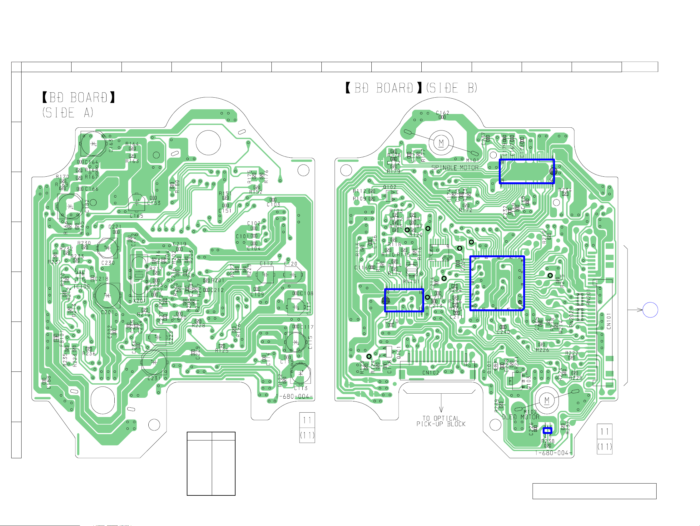
6-5. PRINTED WIRING BOARD – BD Section – • See page 15 for Circuit Boards Location.
1 2 3 4 5 6 7 8 9 10 11 12 13
A
B
IC102
C
D
E
TP (DVC)
TP (FEI)
IC103
IC104
TP (RFAC)
TP (TEO)
TP (RFDC)
TP (FEO)
IC101
TP (XPCK)
A
VMP
BOARD
CN501
(Page 20)
F
TP
(VC)
25
G
H
• Semiconductor
Location
Ref. No. Location
D101 F-10
IC101 E-10
IC102 B-11
IC103 E-8
IC106 H-11
Q101 F-8
Q103 G-10
IC106
(A-MAX.3)
There are a few cases that the part printed on
this diagram isn’t mounted in this model.
1616
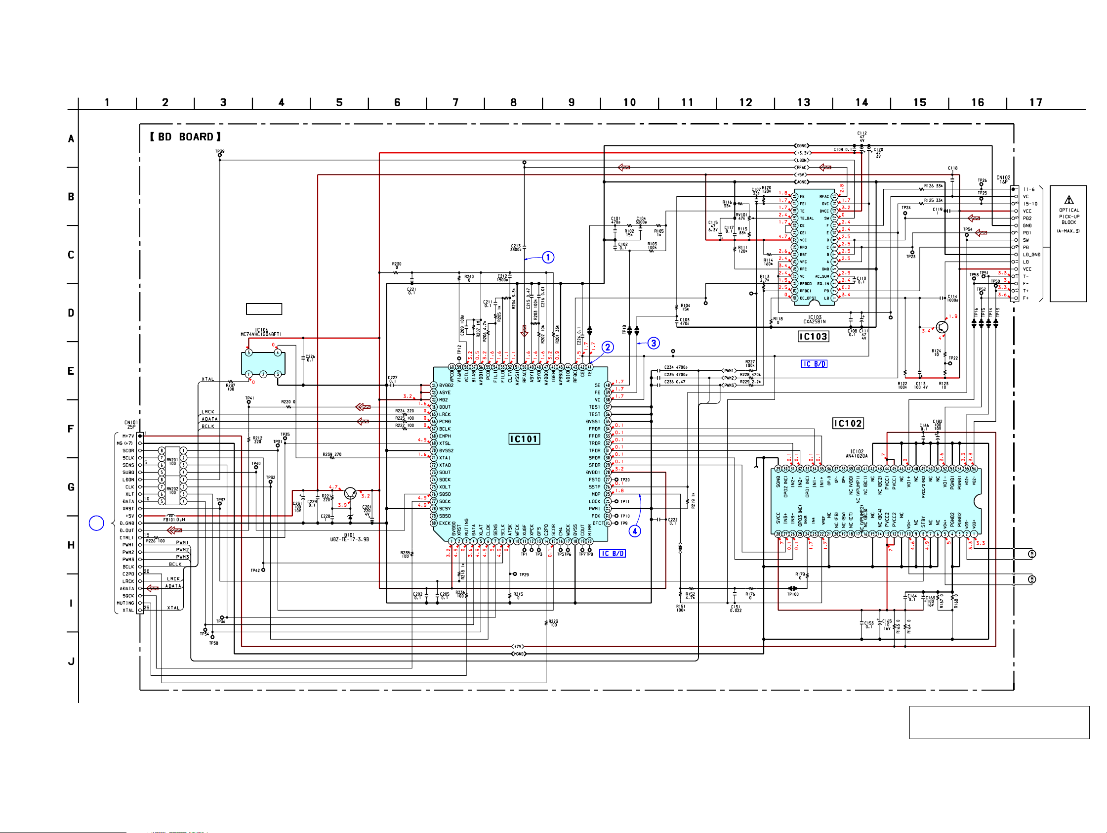
6-6. SCHEMATIC DIAGRAM – BD Section – • See page 28 for Waveforms. • See page 29 for IC Block Diagrams.
TP (RFAC)
IC 106
OSC BUFFER
3.2
(TEO)
MCE-SV7
TP
(FEI)
TP (RFDC)
Q101
AUTOMATIC
POWER CONTROL
TP
(VC)
TP
(FEO)
TP
TP (DVC)
RF AMP,
FOCUS/TRACKING ERROR AMP
Q101
2SB710A
A
VMP
BOARD (1/3)
CN501
(Page 21)
Q103
2SD1664
+3.3V
REGULATOR
DIGITAL SIGNAL PROCESSOR,
DIGITAL SERVO PROCESSOR
IC101
CXD3068Q
TP
(XPCK)
FOCUS/TRACKING COIL DRIVE,
SPINDLE/SLED MOTOR DRIVE
M102
(SLED)
M101
(SPINDLE)
The components identified by mark 0 or dotted
line with mark 0 are critical for safety.
Replace only with part number specified.
1717
 Loading...