

Sony MCEK-750 Service manual
MCE-K550/K750
SERVICE MANUAL
PHOTO: MCE-K750
SPECIFICATIONS
E Model
Chinese Model
Model Name Using Similar Mechanism MCE-S70
CD Mechanism Type CDM14-5BD24
Base Unit Type BU-5BD24
Optical Pick-up Type KSS-213B/S-N
VIDEO CD player
Laser Semiconductor laser
Wavelength 780-790nm
Signal format system NTSC, PAL
Frequency response 2Hz to 20kHz±1dB
Signal-to-noise ratio More than 94dB
Outputs
AUDIO OUT
VIDEO OUT
S VIDEO OUT
(K750)
PHONES
Inputs
MIC 1,
MIC 2
Jack
type
Phono
jack
Phono
jack
4-pin mini
DIN
Phono
jack
Jack
type
Phone
jacks
Maximum
output
level
2V
(at 50 kilohms)
1Vp-p
Y:1Vp-p
C:0.286Vp-p
10mW
Maximum
input
level
100mVp-p
Load impedance
Over 10 kilohms
75 ohms, unbalanced,
sync negative, white
peak
75 ohms, unbalanced,
sync negative
32ohms
Load impedance
600ohms
General
Power requirements (model for Chinese)
220-240V AC, 50/60Hz
(model for other countries)
110-120V or 220-240V A C,
adjustable, 50/60Hz
Power consumption K550:21W, K750:24W
Dimensions (approx.) 430×108×350mm
(w/h/d) inchl. projecting parts
Mass (approx.) 4.4kg
Supplied accessories
Audio and video connecting cord (1)
Remote commander (remote) RMT-K750V/K550V (1)
Sony SUM-3 (NS) battery (2)
Plug adaptor (1) (except model for China)
Desing and specifications are subject to change without notice.
VIDEO CD PLAYER
MICROFILM
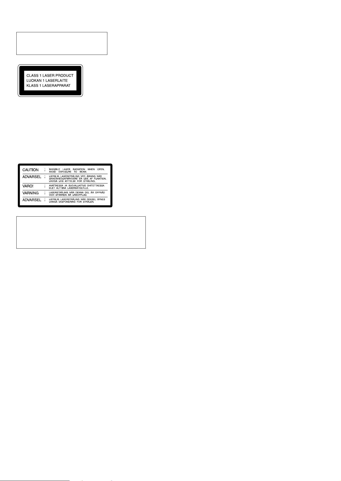
The laser component in this product is
capable of emitting radiation exceeding
the limit for Class 1.
This appliance is classified as
a CLASS 1 LASER product.
The CLASS 1 LASER
PRODUCT MARKING is
located on the rear exterior.
This caution label is located inside
the unit.
CAUTION
Use of controls or adjustments or performance of
procedures other than those specified herein may result in
hazardous radiation exposure.
Notes on chip component replacement
• Never reuse a disconnected chip component.
• Notice that the minus side of a tantalum capacitor may be
damaged by heat.
TABLE OF CONTENTS
1. SERVICING NOTE ················································ 3
2. TEST MODE ·································································· 4
3. GENERAL ······································································ 6
4. DISASSEMBLY
4-1. CABINET··········································································· 7
4-2. BASE UNIT (BU-5BD24) ················································· 7
5. ELECTRICAL ADJUSTMENTS ····························· 8
6. DIAGRAMS
6-1. CIRCUIT BOARDS LOCATION ····································10
6-2. BLOCK DIAGRAM — BD SECTION — ······················ 11
6-3. BLOCK DIAGRAM — MAIN SECTION —·················13
6-4. SCHEMATIC DIAGRAM — BD SECTION —············· 16
6-5. PRINTED WIRING BOARD — BD SECTION —········ 19
6-6. PRINTED WIRING BOARD
— VIDEO SECTION —················································· 21
6-7. SCHEMATIC DIAGRAM
— VIDEO SECTION —·················································· 23
6-8. SCHEMATIC DIAGRAM
— DIAPLAY SECTION — ············································· 27
6-9. PRINTED WIRING BOARD
— DISPLAY SECTION— ··············································· 31
6-10. PRINTED WIRING BOARD — MAIN SECTION—··· 33
6-11. SCHEMATIC DIAGRAM — MAIN SECTION— ········· 35
6-12. IC BLOCK DIAGRAMS ················································· 38
6-13. IC PIN FUNCTION ························································· 41
7. EXPLODED VIEWS
7-1. CASE SECTION ······························································ 45
7-2. CHASSIS SECTION························································ 46
7-3. MECHANISM DECK SECTION (CDM14M-5BD24)··· 47
7-4. BASE UNIT SECTION (BU-5BD24) ····························· 48
8. ELECRICAL PARTS LIST ······································ 49
SAFETY-RELATED COMPONENT WARNING!!
COMPONENTS IDENTIFIED BY MARK ! OR DOTTED LINE WITH
MARK ! ON THE SCHEMATIC DIAGRAMS AND IN THE PARTS
LIST ARE CRITICAL TO SAFE OPERATION. REPLACE THESE
COMPONENTS WITH SONY PARTS WHOSE PART NUMBERS
APPEAR AS SHOWN IN THIS MANUAL OR IN SUPPLEMENTS
PUBLISHED BY SONY.
— 2 —
SECTION 1
SERVICING NOTE
SELF-DIAGNOSIS
This model has the self-diagnosis function for the video and audio
decoder sections.
Immediately after the power on, the self-diagnosis function searches
each operation of IC’s around the mechanism control microcomputer
(IC504).
The LED (D502) on the VIDEO board indicates their results.
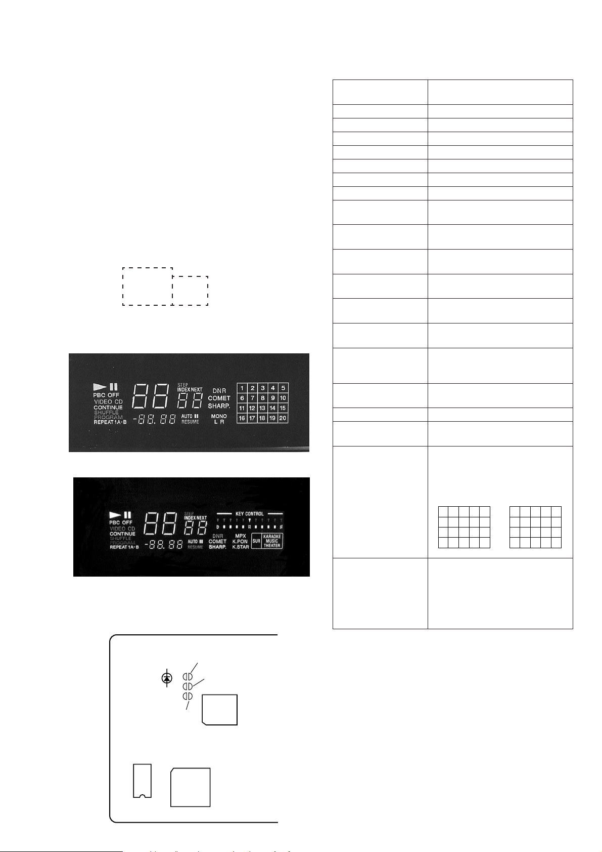
LED (D101) INDICATION
Light
1 Time blinking (Repeatedly)
2 Time blinking (Repeatedly)
[VIDEO BOARD] — SIDE A —
D502
SL503
SL502
SYMPTOM
No error
Video decoder error
(IC503)
Video RAM error (IC502)
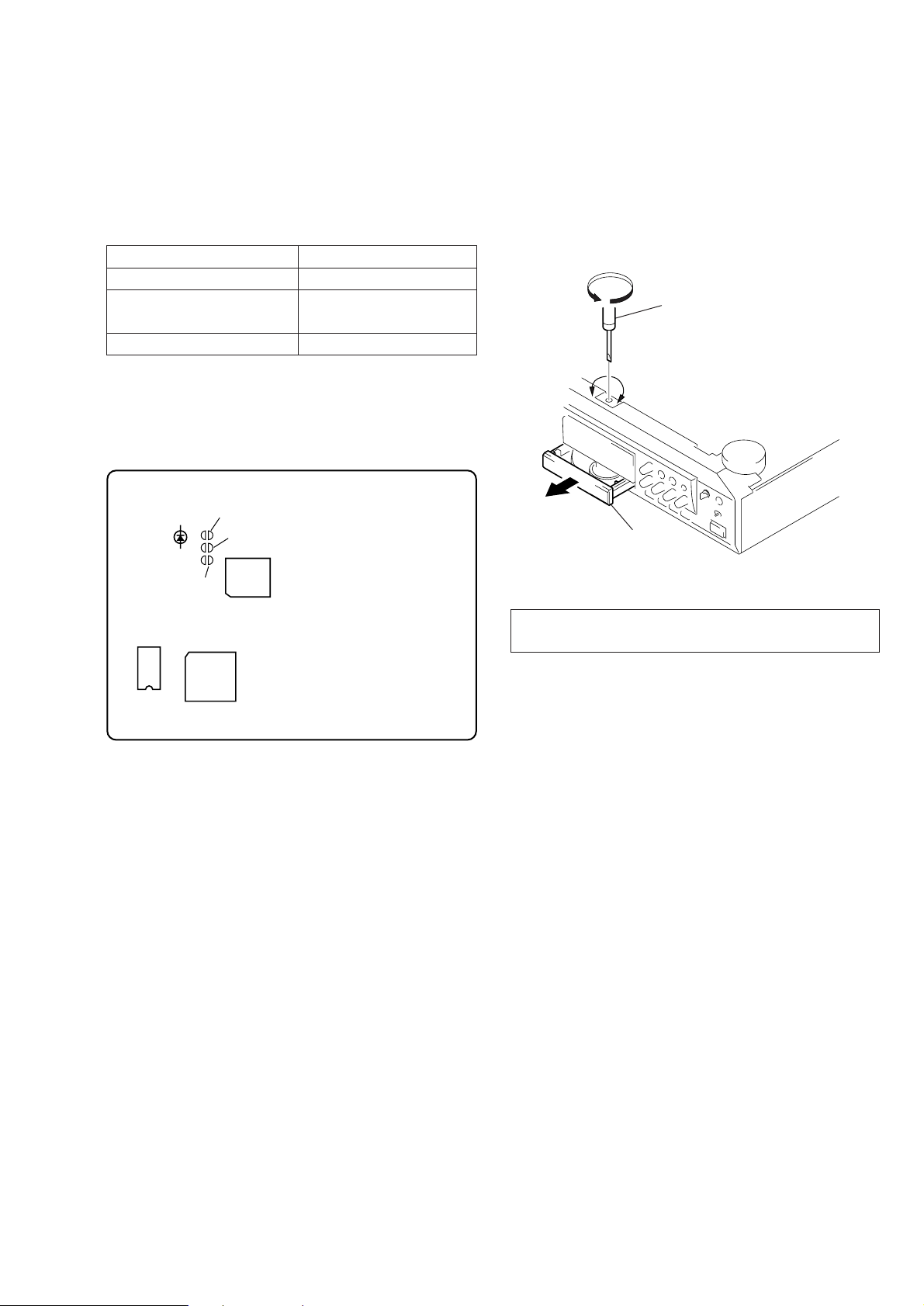
HOW TO OPEN THE DISC TRAY WHEN POWER SWITCH
TURNS OFF
Insert a screwdriver into the aperture of the unit bottom, and turn in
the direction of arrow (to OUT direction).
*
T o close the disc tab le, turn the screwdriver in the re verse direction
(to IN direction).
Screwdriver
OUT
IN
Pull out disc table.
IC502
SL501
IC503
IC504
NOTES ON HANDLING THE OPTICAL PICK-UP BLOCK
OR BASE UNIT
The laser diode in the optical pick-up block may suffer electrostatic
break-down because of the potential difference generated by the
charged electrostatic load, etc. on clothing and the human body.
During repair, pay attention to electrostatic break-down and also
use the procedure in the printed matter which is included in the
repair parts.
The flexible board is easily damaged and should be handled with
care.
NOTES ON LASER DIODE EMISSION CHECK
The laser beam on this model is concentrated so as to be focused on
the disc reflective surface by the objective lens in the optical pickup block. Therefore, when checking the laser diode emission,
observe from more than 30 cm away from the objective lens.
LASER DIODE AND FOCUS SEARCH OPERATION
CHECK
Carry out the “S curve check” in “CD section adjustment” and check
that the S curve waveform is output three times.
— 3 —
SECTION 2
TEST MODE
VIDEO CD COLOR-BARS MODE
On this mode, the data of the color-bars signal as a picture signal
and the 1kHz sine wave signal as a sound signal are output by the
mechanism control microcomputer (IC504) for video CD signal
check. When measurement of the voltage and waveform on the
MAIN board, perform it in this mode.
For reference, the color-bars signal can be observed at J103 (VIDEO
OUT) and the sound signal can be observed at J104 (AUDIO OUT)
using an oscilloscope.
1. Connect the SL503 (C BAR (MICON)) on the VIDEO board
with solder.
2. Turn the power on.
3. After measuring, remove the soldering installed.
SERVO CHECK MODE
1. Connect the SL502 on the VIDEO board with solder.
2. Turn the power on.
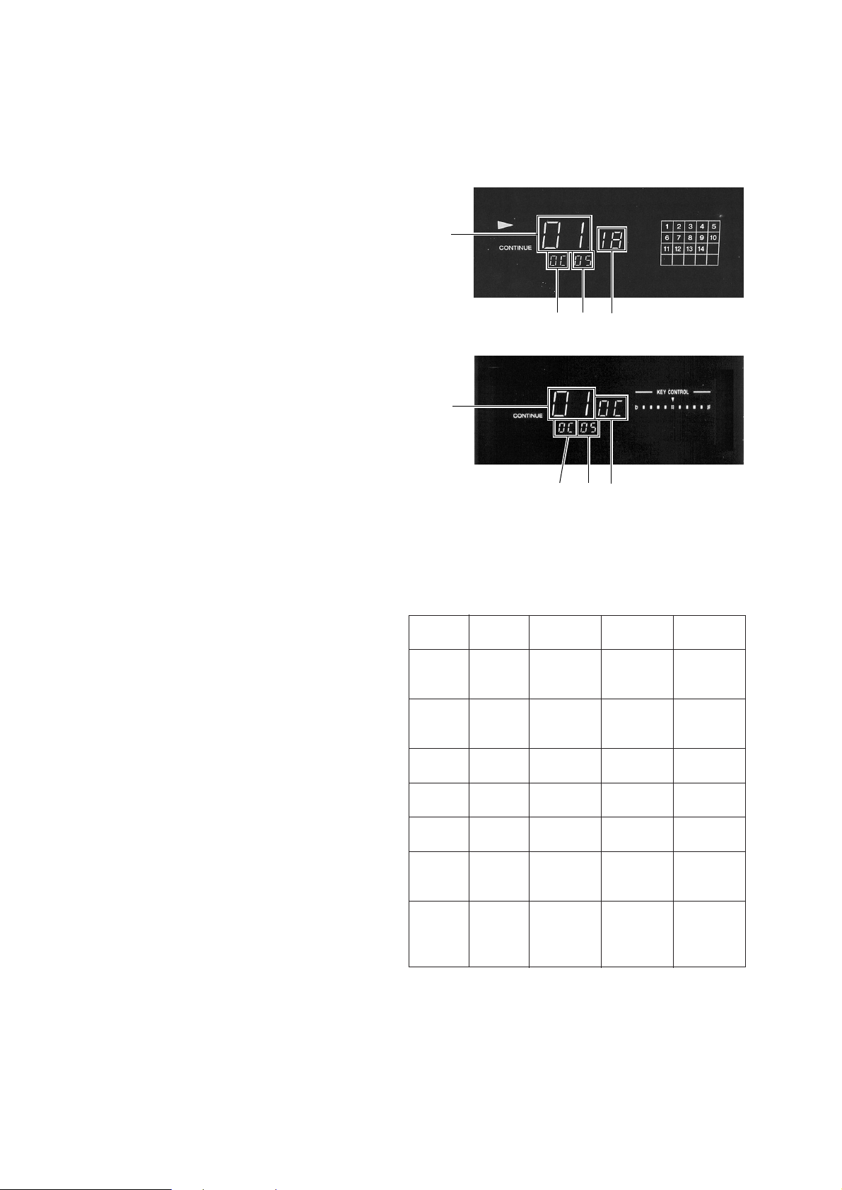
TRACK
MIN SEC INDEX
TRACK
MIN SEC INDEX
Initial display (K550)
Initial display (K750)
1) Coefficient display and gain display
The following hexadecimal data is displayed on the FL tube
when the JOG SELECTOR key is pressed. Every pressing of
the JOG SELECTOR key toggles between the following
displays.
Display
position→
Display
mode 1
Display
mode 2
Display
mode 3
Display
mode 4
Display
mode 5
Display
mode 6
Display
mode 7
TRACK
01
02
03
04
05
06
07
INDEX
FB POINT
(when jitter
is minimum)
00
TRVSC
RESISTER
VC
OFFSET
FCS AUTO
GAIN
RF PEAK –
RF
BOTTOM
Set the
present FB
REGISTER
value
MIN
AUT O F B
POINT
FB upper
limit
00
FE
OFFSET
00
RF PEAK
00
RF JITTER
MINIMUM
VALUE
FB lower
limit
TE
RESISTER
RF
OFFSET
TRK AUTO
GAIN
RF
BOTTOM
Present RF
JITTER
value
SEC
— 4 —
2) Pressing of the DNR/COMET key toggles between ON and
OFF of the tracking and sled servo.
3) Pressing the PLAY MODE key (KARAOKE PON in K750)
during playback increases the FB value (every 4 steps).
Pressing the REPEAT key (SURROUND in K750) decreases
the FB value (every 4 steps).
4) Pressing the ACTIVE key toggles between the normal speed
and double speed.
5) Pressing the RETURN key toggles between the up FIL and
NO FIL.
6) Pressing A⇔B key performs re-measurement of focus bias.
Lighting of All Fluorescent Indicator Tube
Displays and Key Check Mode
1. Connect SL501 on the VIDEO board with solder.
2. Turn the power on.
3. All the Fluorescent Indicator tube displays light up.
4. Press any button to enter the key check mode. In the key check
mode, each time a button is pressed, figures displayed on the
Fluorescent Indicator tube displays increase. Howev er, f igures
will not increase for buttons which have been pressed once.
The button number corresponding to the button pressed will
also be displayed. Button numbers are displayed only while
the corresponding buttons are pressed.
5. After the test mode, remove the soldering installed.
7-segment display
8888
n
Count up display
Initial display (K550)
n
Button number display
Button Name
NEXTˆ
§OPEN/CLOSE
RETURN
PREV
º
‚
DNR
MPX (K750)
L/R/STEREO (K550)
SURROUND (K750)
REPEAT (K550)
KEY CONTROL N
(K750)
KARAOKE STAR
(K750)
KEY CONTROL #
(K750)
KEY CONTROL ˜
(K750)
KARAOKE PON
(K750)
PLAY MODE (K550)
JOG SELECTOR
(PUSH SELECT)
ACTIVE/COMET
p
∏
Button Number (Displayed only
while a button is pressed.)
Figure 0E
Figure 16
Figure 30
Figure 31
Figure 33
Figure 34
Figure 48
Figure 50
Figure 5d
Figure 67
Figure 68
Figure 6b
Figure 6c
Figure 77
Figure 81
Figure 88
All Fluorescent Indicator tube
displays light up
Music calendar light up alternately
(K550)
(odd numbor to even number)
KEY indicater light up alternately
(K750)
↔
24
68
12 14
16 18
10
20
13
79
11 13
17 19
5
15
Initial display (K750)
[ VIDEO BOARD ] — SIDE A —
D502
IC502
SL503
SL501
IC503
SL502
IC504
— 5 —
·
7-segments displays light up
alternately
The odd number digits and the even
number digit of the upper 7-segments
displays and the lower 7-segments
displays light up alternately.
Location of Parts and Controls
Front Panel
SECTION 3
GENERAL
!ª
!•
1
2
!¶
!§
3
!¢!∞
1 STANDBY botton
2 KEY CONTROL botton (K750 MODEL)
3 KARAOKE STAR botton (K750 MODEL)
4 OPEN/CLOSE botton
5 RETURN/PREV/NEXT botton
6 DNR/COMET botton
7 ACTIUVE botton
8 ) botton
9 0 botton
!º JOG SELECTOR
Video CD
4567
8
9
!¡!™!£
!º
!¡ p botton
!™ P botton
!£ · botton
!¢ MPX/KARAOKE PON/SURROUND botton (K750
MODEL)
L/R/STEREO/PLAY MODE/REPEAT botton
(K550 MODEL)
!∞ ECHO LEVEL/MIC 1 LEVEL/MIC 2 LEVEL/
VOCAL LEVEL/MUSIC LEVEL
!§ MIC1/MIC2 jack
!¶ MIC CONTROL jack (K750 MODEL)
!• PHONES jack-LEVEL
!ª MODE switch (K750 MODEL)
Rear Panel
@º @¡ @™ @£ @¢ @∞
K750
MODEL
@º MUSIC LEVEL switch (K550 MODEL)
@¡ AUDIO OUT jack
@™ VIDEO OUT jack
@£ S VIDEO OUT jack (K750 MODEL)
@¢ COLOR SYSTEM switch
@∞ VOLTAGE SELECTOR switch (Singapore, Malaysia, Taiwan MODEL)
— 6 —
SECTION 4
DISASSEMBLY
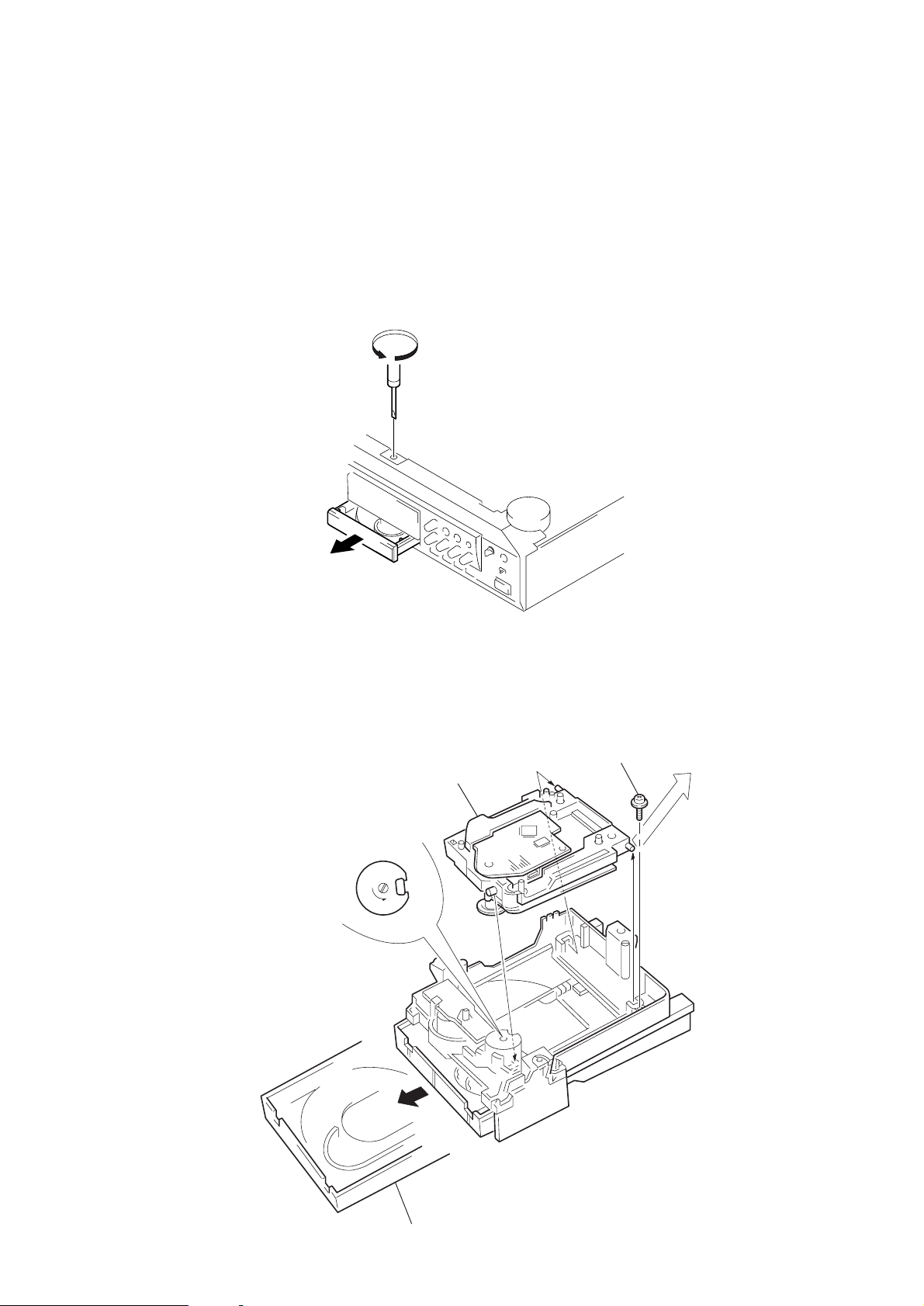
Note: Follow the disassembly procedure in the numerical order given.
4-1. CABINET
• In order to remove the front panel block when the power supply
does not turn on, rotate the cam with screwdriver as the figure
shows, and the disk table will be moved.
Then pull out the disk table by your hand to remove the loading
panel. After that take out the front panel block.
Screwdriver
4-2. BASE UNIT (BU-5BD24)
1
Turn the cam to the
direction of arrow
(counter clock wise)
by screwdriver
Pull out disk table
BU-5BD24
3
Yoke bracket
4
Remove the MD (BU-5BD24)
to the direction of arrow.
2
Take off the disk table.
— 7 —
SECTION 5
ELECTRICAL ADJUSTMENTS
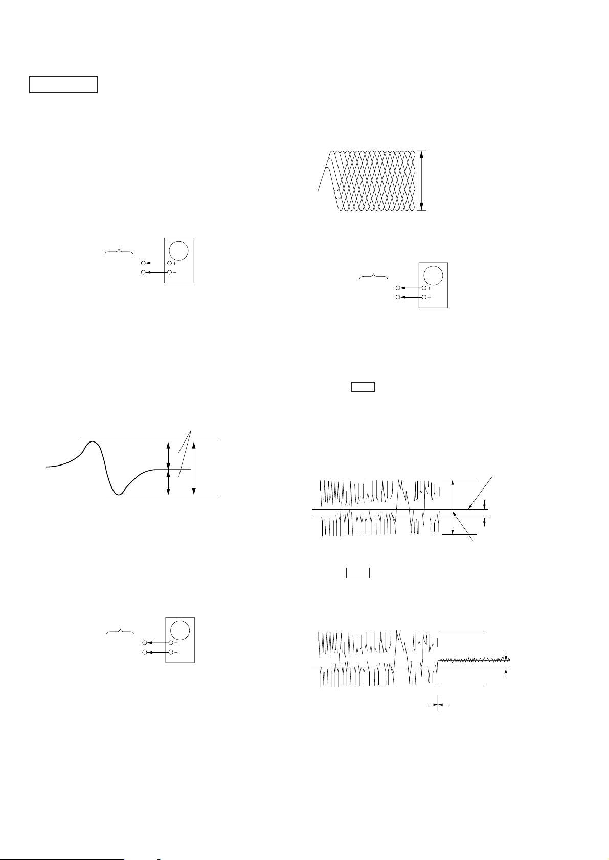
CD SECTION
Note :
1. CD Block is basically designed to operate without adjustment.
Therefore, check each item in order given.
2. Use YEDS-18 disc (3-702-101-01) unless otherwise indicated.
3. Use an oscilloscope with more than 10MΩ impedance.
4. Clean the object lens by an applicator with neutral detergent
when the signal level is low than specified value with the
following checks.
S Curve Check
oscilloscope
BD board
TP (FE)
TP (VC)
Procedure :
1. Connect oscilloscope to test point TP (FE) on BD board.
2. Connect between test point TP (FEI) and TP (VC) by lead wire.
3. Turned Power switch on.
4. Put disc (YEDS-18) in and turned Power switch on again and
actuate the focus search. (actuate the focus search when disc
table is moving in and out.)
5. Check the oscilloscope waveform (S-curve) is symmetrical
between A and B.
And confirm peak to peak level within 3±1 Vp-p.
S-curve waveform
symmetry
A
within 3 ± 1 Vp-p
B
Note : A clear RF signal waveform means that the shape “◊” can
be clearly distinguished at the center of the waveform.
RF signal waveform
VOLT/DIV : 200mV
TIME/DIV : 500ns
level : 1.3 p-p
+0.25
–0.20
E-F Balance (Traverse) Check
oscilloscope
BD board
TP (TE)
TP (VC)
Procedure :
1. Connect oscilloscpe to test point TP (TE) on BD board.
2. Turned Pow er switch on.
3. Connect the SL502 on the VIDEO board with solder.
4. Put disc (YEDS-18) in to play the number two track.
5. Press the DNR button. (The tracking servo and the sledding
servo are turned OFF.)
6. Check the level B of the oscilliscope's waveform and the A
(DC voltage) of the center of the Traverse waveform.
Confirm the following :
A/B x 100 = less than ± 22%
Traverse wavefor m
Center of the waveform
B
6. After check, remove the lead wire connected in step 2.
Note : • Try to measure several times to make sure than the ratio
of A : B or B : A is more than 10 : 7.
• Take sweep time as long as possible and light up the
brightness to obtain best waveform.
RF Level Check
oscilloscope
BD board
TP (RF)
TP (VC)
Procedure :
1. Connect oscilloscope to test point TP (RF) on BD board.
2. Turned Power switch on.
3. Put disc (YEDS-18) in to play the number five track.
4. Confirm that oscilloscope waveform is clear and check RF
signal level is correct or not.
±
0.6 Vp-p
A (DC voltage)
0V
level : 1.3
7. Press the DNR button. (The tracking servo and sledding servo
are turned ON.) Confirm the C (DC voltage) is almost equal to
the A (DC voltage) is step 6.
Traverse wavefor m
0V
T rac king servo
Sled servo
OFF
T racking servo
Sled servo
ON
C (DC
voltage)
8. Remove the soldering installed in step 3.
— 8 —
SECTION 6
DIAGRAMS
Adjustment Location :
[ BD BOARD ] — SIDE A —
1
10
20
IC103
11
IC101
(RF) (VC)
(FE)
(FEI)
VIDEO SECTION
Frequency adjustment (NTSC)
1. Connect the frequenc y counter to c hec k point of the VIDEO
board.
VIDEO board
27.0 MHz
GND
frequency counter
2. Color system switch (S300) select to NTSC and turn the
POWER switch ON.
3. Adjust CT503 of the VIDEO boar d so that the frequenc y
counter read 27.0MHz ± 80Hz at ST OP condition.
Frequency adjustment (PAL)
1. Connect the frequenc y counter to c hec k point of the VIDEO
board.
VIDEO board
27.0 MHz
GND
frequency counter
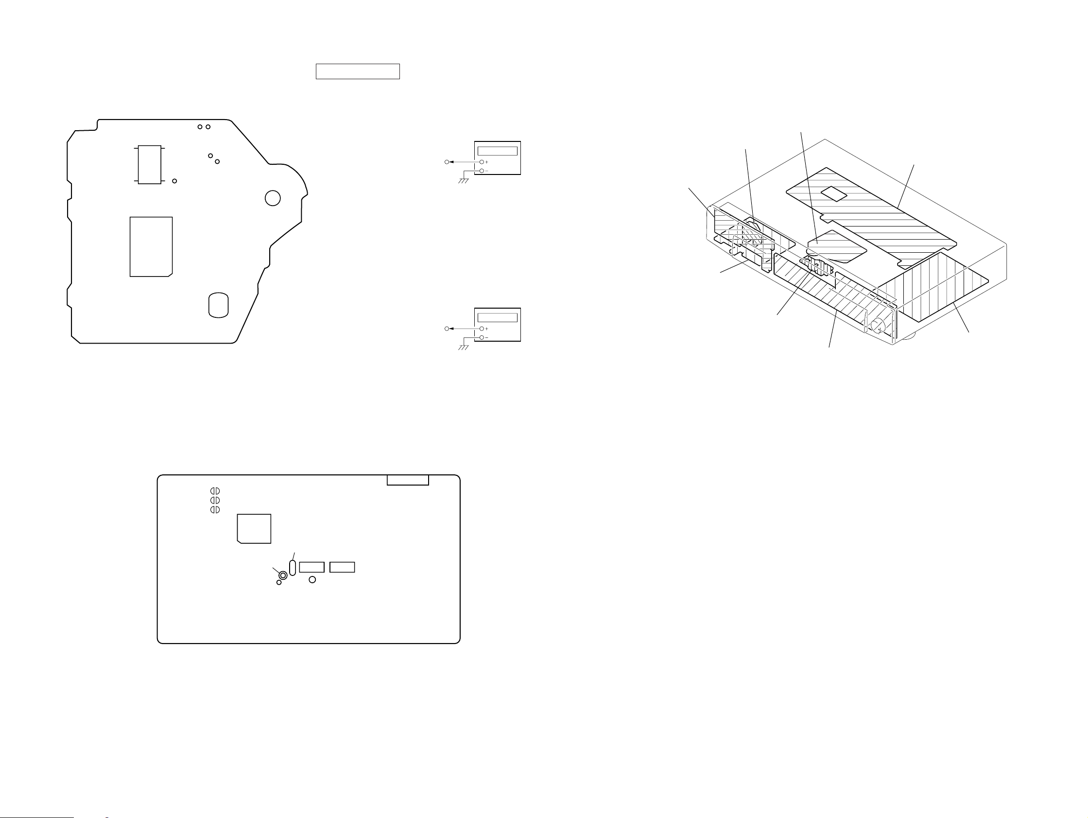
6-1. CIRCUIT BOARDS LOCATION
BD board
CN board
MAIN board
VOL board
MIC board
LOADING board
VIDEO board
DISPLAY board
[ VIDEO BOARD ] — SIDE A —
SL503
SL502
SL501
IC504
CT503
GND
2. Color system s witch (S300) select to P AL and turn the PO WER
switch ON.
3. Adjust CT503 of the VIDEO boar d so that the frequenc y
counter read 27.0MHz ± 80Hz at ST OP condition.
CN504
X505
IC513IC512
27MHz
— 9 — — 10 —
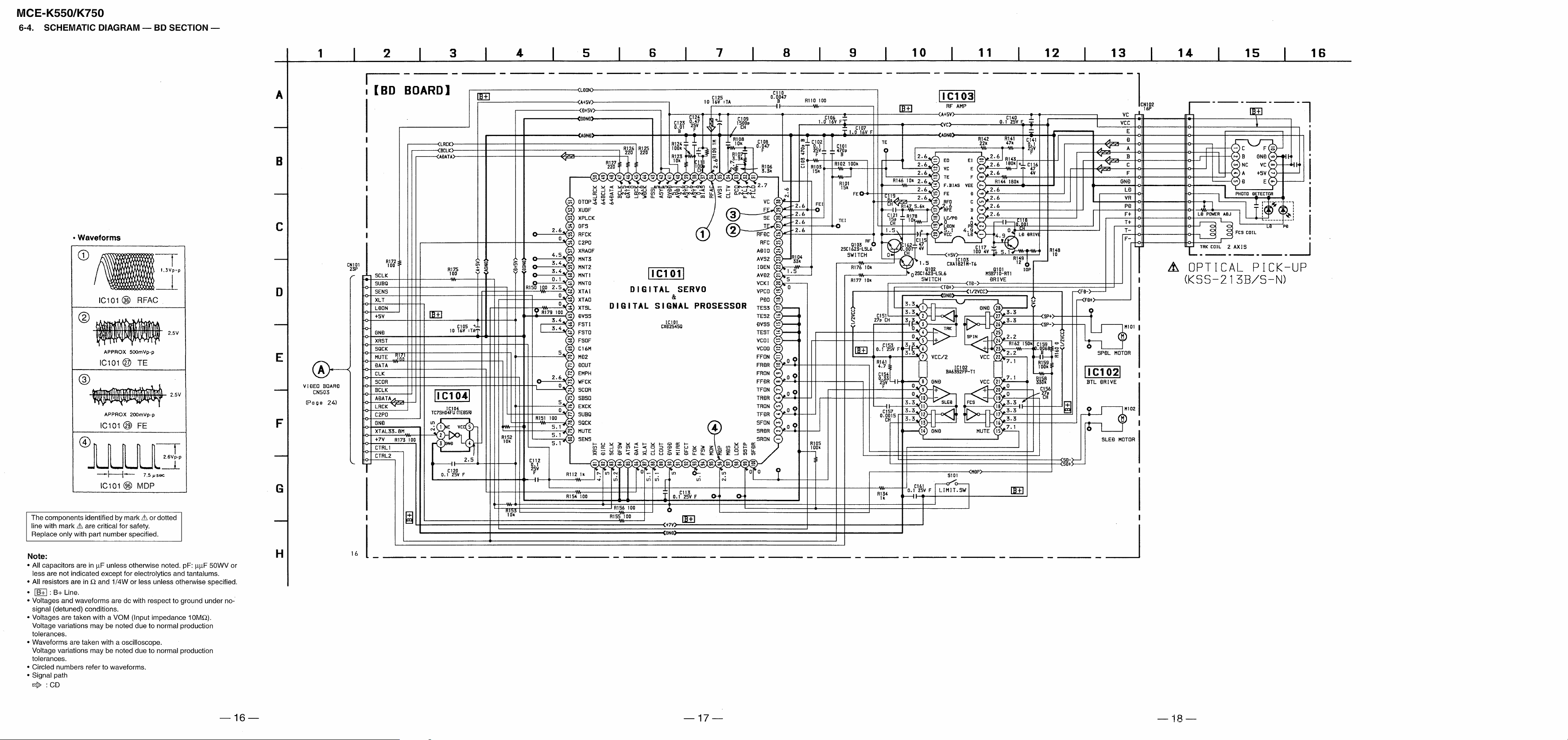
MCE-K550/K750
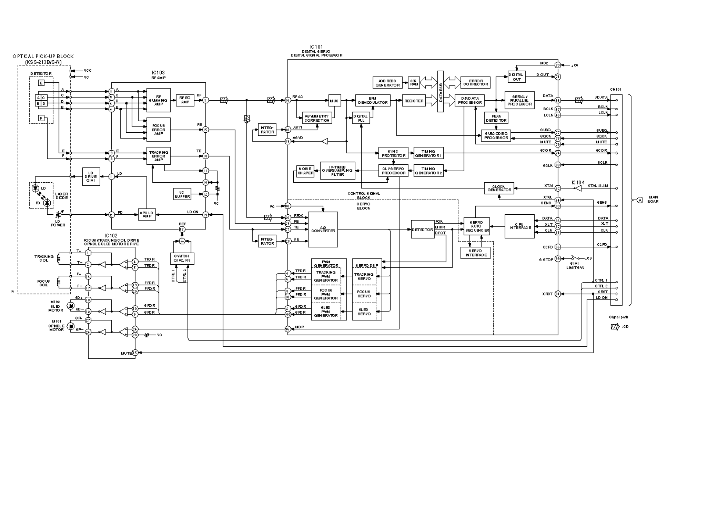
6-2. BLOCK DIAGRAM — BD SECTION —
— 11 — — 12 —
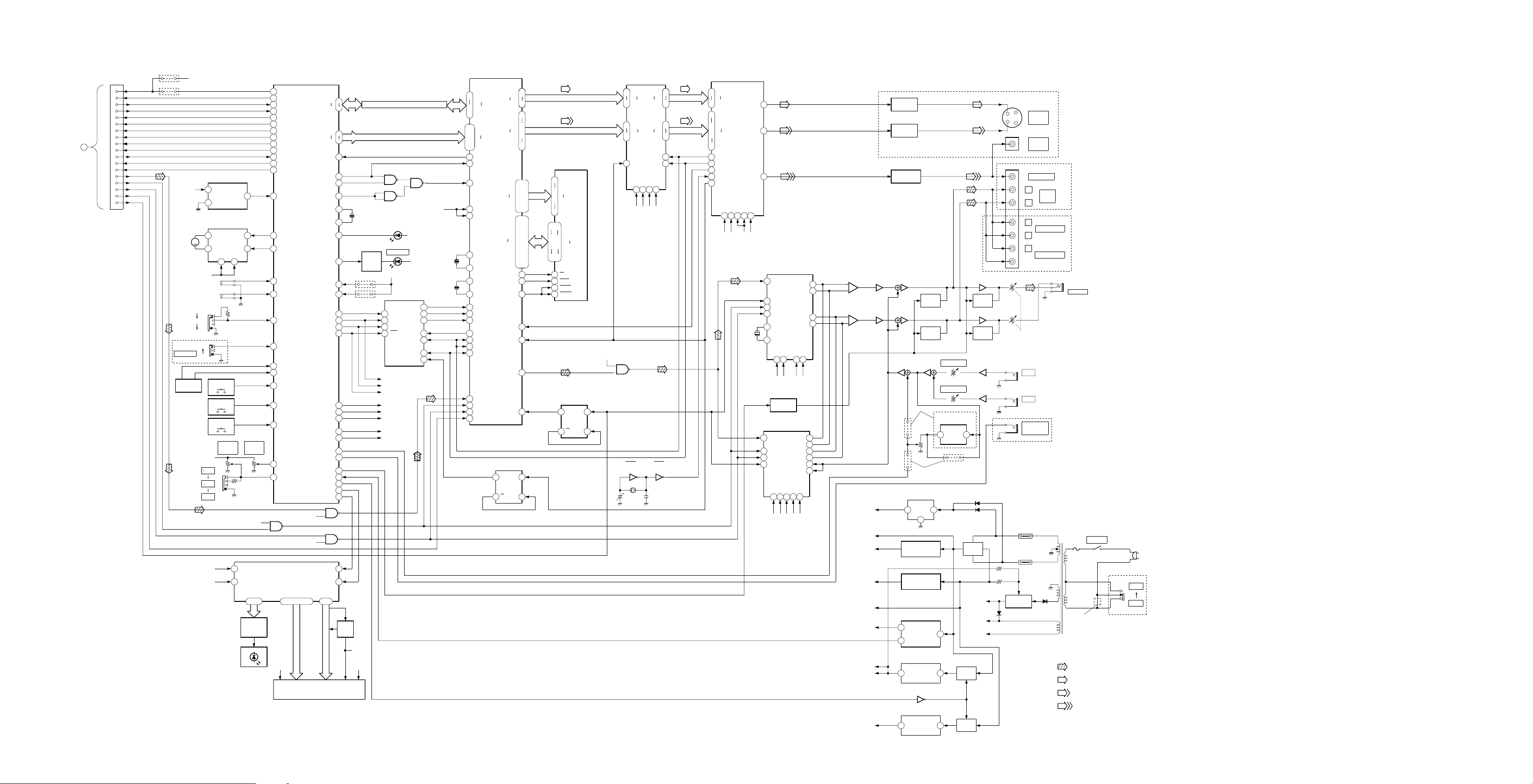
6-3. BLOCK DIAGRAM — MAIN SECTION —
MCE-K550/K750
BD
BOARD
8
4
MPEG DECODER
7
HD0
13
HD7
.
16
119
.
A0
120
.
5
A3
.
6
XHIRQ
117
XWR
116
XHCS
114
118
XRST
XSGRST
97
XTL0I
3
XTL0O
2
XTL2I
107
XTL2O
106
OSD R
59
OSD G
58
OSD B
57
XOSDEN
56
92
H SYNC
CBLNK/FSC
95
V SYNC
93
DATI
111
BCKI
112
LRCI
110
C2PO
109
IC503
63
R/Cr0
R/Cr7
70
71
73
G/Y0
.
76
G/Y7
80
18
.
24
.
20
MA0
.
21
.
23
.
19
MA8
.
22
.
17
33
54
39
.
.
52
41
.
.
50
43
.
.
MD0
48
47
.
.
49
46
MD15
.
.
51
42
.
.
53
40
.
.
55
38
XMWE
35
XRAS
34
XCAS0
37
FID/FHREF
94
DCLK
89
DATA
100
FSXI
103
QCK
5
3
DIVIDER
IC513(2/2)
DQ
62
Y/C PROCESSOR
IC506
27
8
8
DRAM
IC502
16
19
A0
.
9
22
A8
26
2
31
5
34
DQ1
.
.
16
36
7
DQ16
39
10
W
13
RAS
14
28
UCAS
LCAS
29
+5V(D)
384FS
QCK
9
11
DIVIDER
IC513(1/2)
DQ
812
20
18
11
100
13
12
IC505(4/4)
12 3
27MHz
C/RI0
CRI7
Y/GI0
Y/GI7
DCLK
31
11
CLOCK CONT
X202
SDI
SO1
30
IC202
C/RO0
CRO7
Y/GO0
Y/GO7
H SYNC
V SYNC
XSCK
XRST
93 29
CLK1
XRST
51
58
60
67
98
97
XCS
DNR CS
4
8
8
10BIT D/A CONV
18
C0
C7
11
9
Y0
6
.
4
Y7
1
H SYNC
60
V SYNC
59
FID
62
SYS CLK
56
PD CLK
57
48
SI
SO1
49
IC511
SCK
CLK1
55
XRST
C OUT
Y OUT
COMP O
XVRST
51
50
XRST
X504
33MHz
XCS
DVE CS
32
29
24
DIGITAL FILTER
DI
6
3
MLEN
5
BCLK
8
LRCK
XTI
18
XTO
19
23
MUTE SW
DIGITAL FILTER
D/A CONV
SI
92
93
BCK
94
LRCK
14
BFOI
XRST
8
XRST
D/A CONV
IC508
MD
MC
24
SO1
CLK1
Q310
IC510
SCK
RVDT
98
4
SO1
CLK1
L ON
R ON
XRST
22
XRST
AO1N
AO1P
AO2N
AO2P
AIN3
LO3
XLT
1
99
KDSP CS
12
LO
10
14
RO
16
ML
1
DF CS
39
40
33
34
20
21
READY
KDSP RDY
LPF
IC101(1/2)
5
6
3
2
7
1
+10V
+UNREG
-UNREG
-10V
+5V
(UNSW)
+5V(A)
+5V(D)
LPF
IC102(1/2)
5
3
+7V
–5V
7
1
C BUFFER
Y BUFFER
CV BUFFER
LINE AMP
IC103(1/2)
IC103(2/2)
Q331-333
Q341-343
Q371-374
MIX AMP
IC401(2/2)
K550 MODEL
K750 MODEL
REG
3
IC304
RIPPLE FILTER
Q311
RIPPLE FILTER
Q312
UNSWITCHED +5V
IC302
5
OUT
4
RESET
+5V REG
IC301
3
Q309
–5V REG
IC305
3
MUTE
Q100
MUTE
Q200
MIC1 VOL
IC401(2/2)
MIC2 VOL
ECHO UNIT
911
1
2
1
IN
+Vcc+V OUT
1
IN–V OUT
2
RV400
RV401
IC402
OUT
IN
Q305
POWER
SW
POWER
SW
Q313
Q314
HP AMP
IC105(1/2)
IC105(2/2)
MIC AMP
IC400(1/2)
7
MIC AMP
IC400(2/2)
D905
D904
RECT
D906
-30V
(VFDP)
5
MUTE
Q101
MUTE
Q201
VF1
VF2
K750 MODEL
J102
C
S VIDEO
J103
J104
-1
-2
K750 MODEL
ICP900
ICP901
REG CONT
Q900,901
VIDEO
VIDEO OUT
LL
R
L
L
R
L
L
MIC 1
IN
MIC 2
IN
MIC
CONTROL
OUT
OUT
K550 MODEL
AUDIO
OUT
K750 MODEL
AUDIO OUT 1
AUDIO OUT 2
D901
T901
Signal path
J300
PHONES
F901
CHINESE,
: CD
: CHROMA
: Y
: VIDEO
MODEL
S901
POWER
S900
115V
230V
SINGAPORE,
MALAYSIA,TAIWAN
MODEL
AC
IN
Y
CV
L
R
L
R
L
R
RV300
7
13
5
31
D903
24
2
36
1
4
6
37
10
3
5
18
11
19
7
28
27
29
30
52
25
26
90
95
94
IC505(2/4)
10
9
FL DRIVE
MECHA CONTROL
DSP XRST
SCLK
SUBQ
SENS
XLT
LDON
SQCK
MUTE
DATA
CLK
SCOR
CONT1
CONT2
SIRCS
LOAD IN
LOAD OUT
IN SW
OUT SW
N/P SW93
KARAOKE
JOG 1
JOG 2
KEY 0
KEY 191
KEY 292
VOCAL VOL
MUSIC VOL
8
IC701
S1-S24 C1-C6
.
56 - 42
VF1
MICON
IC504
VCDINT
XRW
VCDCS
X OUT
X IN
TEST LED
PWON LED
MODE1
MODE2
OSD CS
SO1
CLK1
XRST
DNR CS
DVE CS
DF CS
KDSP CS
KDSP RDY
ECHO VOL
MIC CONT
AMUTE
XRESET
PWON
FL CS
XBLK
1
2
+5V(D)
IC505(1/4)
IC505(3/4)
5
4
+5V(D)
XBLK
40 - 33
2 - 7
FL700
FLUORESCENT
INDICATOR TUBE
D0
88
8
81
D7
A0
72
4
69
A3
20
IC507
1
46
RD
44
47
13
X502
10MHz
15
73
LED
3
6
C1
GRID
DRIVE
Q401
DRIVE
Q700
K550 MODEL
K750 MODEL
-30V
(VFDP)
VF2
78
53
54
34
31
33
77
100
21
22
49
50
97
89
48
12
38
79
80
61
62
CE
C1
2
12
13
STANDBY
+5V(D)
2
3
1
4
SO1
CLK1
XRST
DNR CS
DVE CS
DF CS
KDSP CS
KDSP RDY
D502
D700
CS
DATA
CLK
PCL
3
11
OSD
IC509
4
5
V CBL
H SYNC
V SYNC
OSC
+5V
(EVER)
+5V
(EVER)
VR
VG
VB
6
XRST
X501
28.63MHz
X503
45MHz
16
17
18
11
20
19
8
K550 MODEL
CN101
A
XRST
SCLK
SUBQ
SENS
XLT
LDON
SQCK
MUTE
DATA
CLK
SCOR
CTRL1
CTRL2
ADATA
BCLK
LRCK
C2PO
384BD
16
K750 MODEL
(EVER)
LOADING
MOTOR
S720
KARAOKE
ENCODER
AUDIO
ADATA
BCLK
LRCK
+5V
S301
ATT
XRST
M
LOAD IN
LOAD OUT
PAL
AUTO
NTSC
ON
OFF
3
2
2
10
+7V
S152
S153
S300
+5V
(EVER)
12dB
9dB
OFF
SO1
CLK1
REMOTE
CONTROL
IC700
MOTOR DRIVE
IC501
OUT1
OUT2
78
K750
MODEL
S700-705
S707-712
S713-719
RV301 RV302
MUSIC
VOL
64
63
R IN
F IN
1
5
6
VOCAL
+5V(D)
DI
CL
Q701-706
D701-706
VOL
S35-40
22 - 17
LED
DRIVE
6
— 13 — — 14 —
— 15 —
 Loading...