

Sony MCEF-808-K Service manual
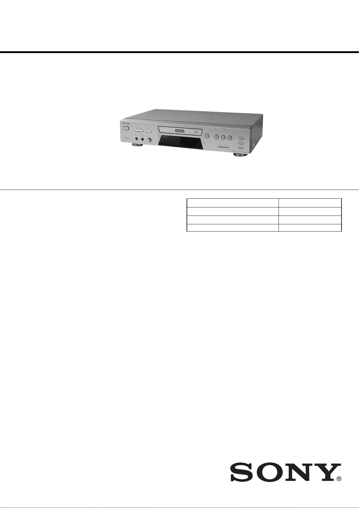
MCE-F808K
SERVICE MANUAL
Ver 1.1 2002. 08
Model Name Using Similar Mechanism NEW
CD Mechanism Type DECK ASSY
Base Unit Type PU BASE
Optical Pick-up Type PICK-UP ASSY
E Model
SPECIFICATIONS
System VIDEO CD player
Laser Semiconductor laser (λ=780nm for CD)
Signal format system NTSC, PAL
Playable discs VIDEO CD, audio CD, MP3 disc
Frequency response 20 Hz to 20 kHz (±1.0 dB)
Signal-to-noise ratio More than 90dB
Outputs
VIDEO OUT (Phono jacks) 1.0 Vp-p 75 ohms, sync negative
AUDIO OUT (Phono jacks) Impedance 47 klilohms, Rated input 2 Vrms
Input
MIC 1, MIC 2 (Phone jacks) 100 mVp-p, 600 ohms
General
Power requirements 220-240 V AC, 50/60 Hz
Power consumption 10W
Dimensions (approx.) 430 × 97.5 × 265 mm (w/h/d) incl. projecting parts
Mass (approx.) 2.8 kg
Supplied accessories
Audio connecting cord (1)
Video connecting cord (1)
Remote commander (remote) RMT-F808V (1)
R6 (size AA) batteries (2)
Design and specifications are subject to change without notice.
Emission duration: continuous
Load impedance over 10 kilohms
9-874-041-02
2002H1600-1
© 2002.08
VIDEO CD PLAYER
Sony Corporation
Home Audio Company
Published by Sony Engineering Corporation
MCE-F808K
TABLE OF CONTENTS
1. SERVICING NOTE·····················································
2. GENERAL ···································································4
3. DISASSEMBLY ·························································· 5
3-1. Top Cabinet ··································································· 6
3-2. VCD Door, Front Panel Section ··································· 6
3-3. CD Mechanism Deck (DECK ASSY) ·························· 7
3-4. MAIN Board, TOTAL Board········································ 7
3-5. FRONT Board, C/SKD Board ······································ 8
3-6. Disk Tray ······································································ 8
3-7. Loading Belt, CD Pwb Assy (Loading) ························ 9
3-8. Pick-Up Assy ································································ 9
4. TROUBLESHOOTING················································· 10
4-1. CD Section ·································································· 10
4-2. MPEG Part Troubleshooting······································· 15
5. DIAGRAMS······································································ 29
5-1. Circuit Boards Location ·············································· 29
5-2. Block Diagrams
– BD Section – ···························································· 30
– MPEG Section – ······················································ 31
– MAIN Section – ······················································· 32
5-3. Printed Wiring Board – MAIN/PANEL Section – ······ 33
5-4. Schematic Diagram – MAIN/PANEL Section – ········ 34
5-5. Printed Wiring Board – TOTAL Section – ················· 35
5-6. Schematic Diagram – TOTAL Section – ···················· 36
5-7. IC Block Diagrams ····················································· 37
5-8. IC Pin Functions ························································· 39
6. EXPLODED VIEWS ······················································ 44
6-1. Cabinet and MAIN FRAME Section ·························· 44
6-2. CD Mechanism Section ·············································· 45
7. ELECTRICAL PARTS LIST ······································· 46
3
Laser component in this product is capable
of emitting radiation exceeding the limit for
Class 1.
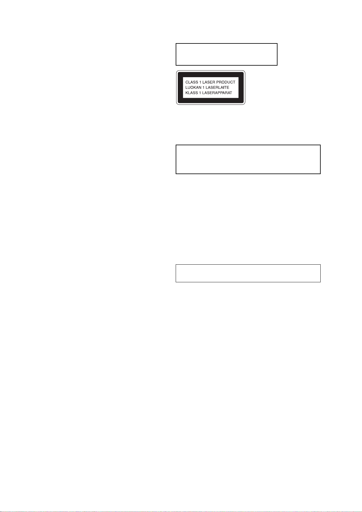
This appliance is classified as a CLASS 1 LASER product. The
CLASS 1 LASER PRODUCT MARKING is located on the rear
exterior.
The following caution label is located inside the unit.
CAUTION
Use of controls or adjustments or performance of procedures
other than those specified herein may result in hazardous radiation
exposure.
Notes on chip component replacement
• Never reuse a disconnected chip component.
• Notice that the minus side of a tantalum capacitor may be
damaged by heat.
Flexible Circuit Board Repairing
• Keep the temperature of soldering iron around 270˚C
during repairing.
• Do not touch the soldering iron on the same conductor of the
circuit board (within 3 times).
• Be careful not to apply force on the conductor when soldering
or unsoldering.
NOTES ON HANDLING THE OPTICAL PICK-UP BLOCK
OR BASE UNIT
The laser diode in the optical pick-up block may suffer electrostatic
break-down because of the potential difference generated by the
charged electrostatic load, etc. on clothing and the human body.
During repair, pay attention to electrostatic break-down and also
use the procedure in the printed matter which is included in the
repain parts.
The flexible board is easily damaged and should be handled with
care.
NOTES ON LASER DIODE EMISSION CHECK
The laser beam on this model is concentrated so as to be focused on
the disc reflective surface by the objective lens in the optical pickup block. Therefore, when checking the laser diode emission,
observe from more than 30 cm away from the objective lens.
The emission check enables continuous checking of the S curve.
LASER DIODE AND FOCUS SEARCH OPERATION
CHECK
Carry out the “S curve check” in “CD section adjustment” and check
that the S curve waveform is output three times.
SAFETY-RELATED COMPONENT WARNING!!
COMPONENTS IDENTIFIED BY MARK 0 OR DOTTED LINE WITH
MARK 0 ON THE SCHEMATIC DIAGRAMS AND IN THE PARTS
LIST ARE CRITICAL TO SAFE OPERATION. REPLACE THESE
COMPONENTS WITH SONY PARTS WHOSE PART NUMBERS
APPEAR AS SHOWN IN THIS MANUAL OR IN SUPPLEMENTS
PUBLISHED BY SONY.
2
SECTION 1
SERVICING NOTE
[HOW TO OPEN THE DISC TRAY WHEN THE MAIN POWER TURNS OFF]
1. Open the top cabinet. (Refer to Section 3-1 “Top Cabimet”)
2. Remove the connector from PN807 on the TOTAL board.
3. Supply +2.8V dc by the unit of DC regulated supply to the connector as shown below.
4. Open the tray in the direction of the arrow.
connector
(PN807)
MCE-F808K
GND
+2.8V
BLUE
3
MCE-F808K
SECTION 2
GENERAL
This section is extracted
from instruction manual.
17 16 15
1
POWER indicator
2
3
button
4
button
5
ECHO button
6
OPEN/CLOSE button
7
SELECT button
5421 3
button
10
PCB ON/OFF switch
11
RETURN switch
12
REPEAT switch
13
14
15
16
NEXT button
PREV button
MIC LEVEL control
MIC 2 jack
109876
121314 11
8
button
9
button
This Player Can Play the
Following Discs
VIDEO CDs Audio CDs
Discs logo
Contents Audio + Video Audio
(moving pictures)
Disc size 12 cm/ 8 cm 12 cm/8 cm
z
The VIDEO CD Player can play MP3 format
recordings on CD-ROM, CD-R or CD-RW
discs. see page 21.
Note on VIDEO CDs
This player conforms to Ver. 1.1 and Ver. 2.0 of
VIDEO CD standards. You can enjoy two kinds of
playback according to the disc type.
17
MIC 1 jack
4
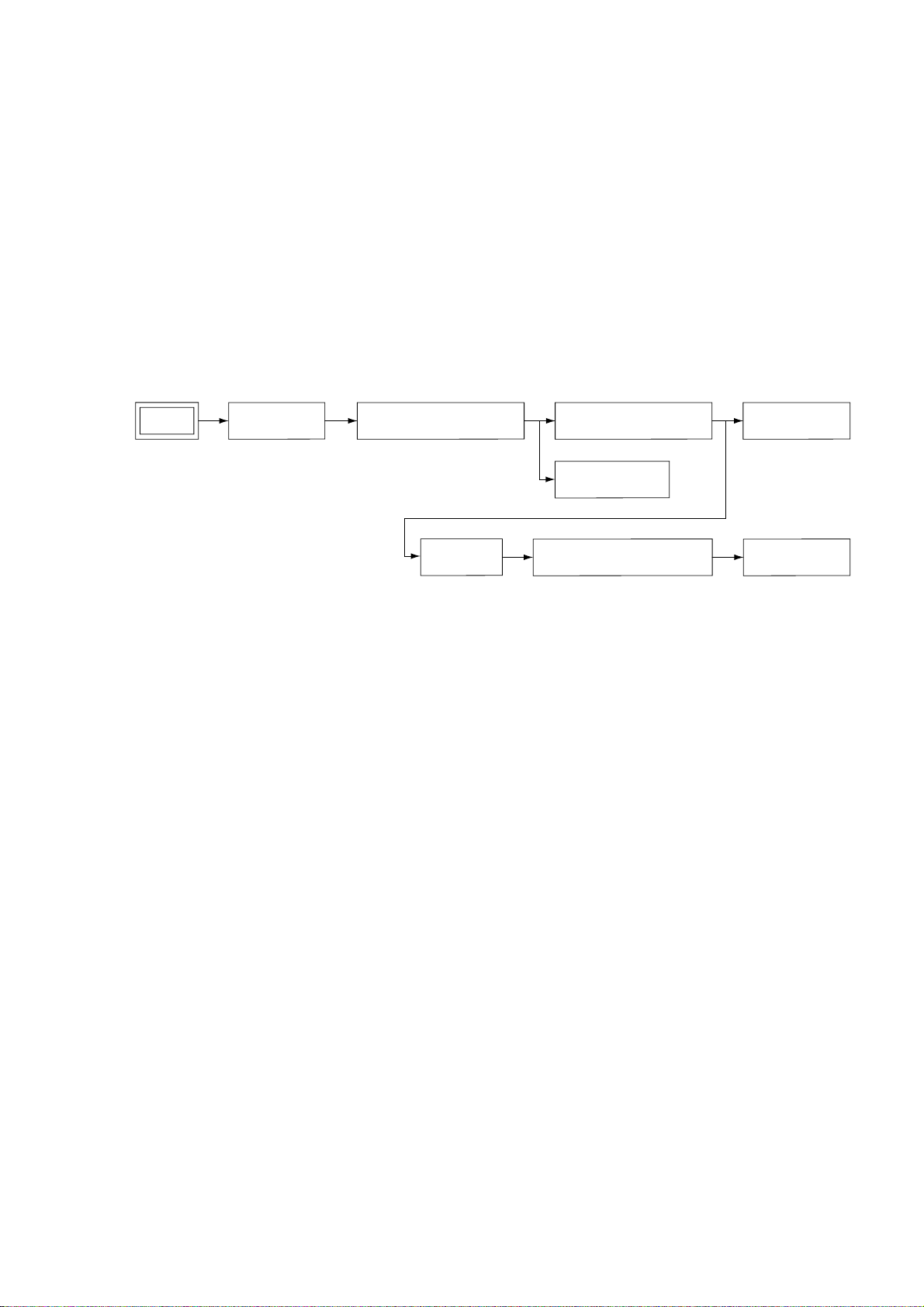
Note : Disassemble the unit in the order as shown below.
MCE-F808K
SECTION 3
DISASSEMBLY
SET
TOP CABINET
VCD DOOR,
FRONT PANEL SECTION
DISK TRAY PICK-UP ASSY
CD MECHANISM DECK
(DECK ASSY)
FRONT BOARD,
C/SKD BOARD
LOADING BELT,
CD PWB ASSY (LOADING)
MAIN BOARD,
TOTAL BOARD
5
MCE-F808K
)
Note : Follow the disassembly in the numerical order given.
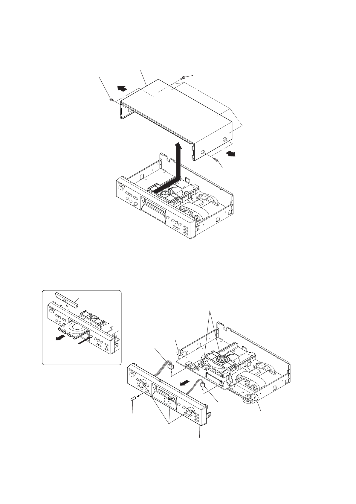
3-1. T op Cabinet
7
two screws
2
(case 3 TP2)
5
top
cabinet
6
1
four screws
(case 3 TP2)
3
(case 3 TP2
4
two screws
3-2. VCD Door, Front Panel Section
2
VCD door
1
Push
OPEN/CLOSE
button.
5
(PN102)
3
volume knob
connector
9
claw
8
three claws
qa
6
two claws
4
connector
(PN103)
7
claw
q;
front panel
section
6
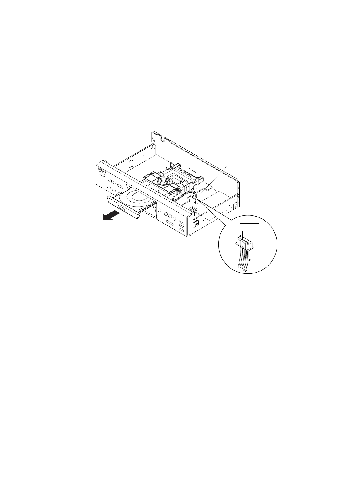
3-3. CD Mechanism Deck (DECK ASSY)
)
1
(TP 3
2
connector
(PN807)
three
screws
×
10)
5
CD mechanism deck (DECK ASSY
4
wire (flat type)
3
connector
(PN803)
MCE-F808K
3-4. MAIN Board, TOTAL Board
6
MAIN board
1
(3
six
screws
×
8)
3
(flat type)
wire
5
connector
(PN813)
4
connector
(PN501)
8
two
screws
(3
×
8)
7
screw
(TP 3
×
16)
9
TOTAL board
2
screw
(TP 3
×
10)
7
MCE-F808K
d
y
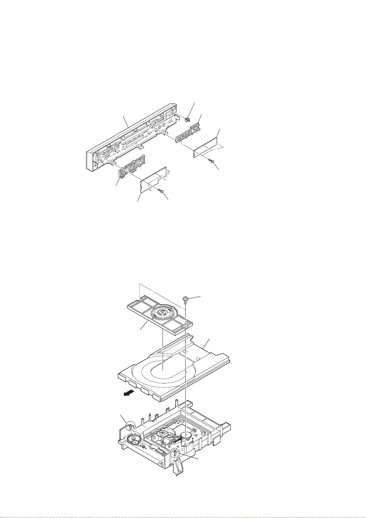
3-5. FRONT Board, C/SKD Board
7
select knob
front panel
4
lens, power
3
power knob
2
FRONT boar
1
three
(TP 3
screws
×
10)
3-6. Disk Tray
6
C/SKD board
4
clamp holder
5
five
(TP 3
screws
×
10)
1
two
screws
(b-tite)
5
disk tra
2
claw
3
claw
8
3-7. Loading Belt, CD Pwb Assy (Loading)
r
1
loading belt
3
pulley gear
4
loading gear
2
6
7
CD pwb assy (loading)
MCE-F808K
claw
claw
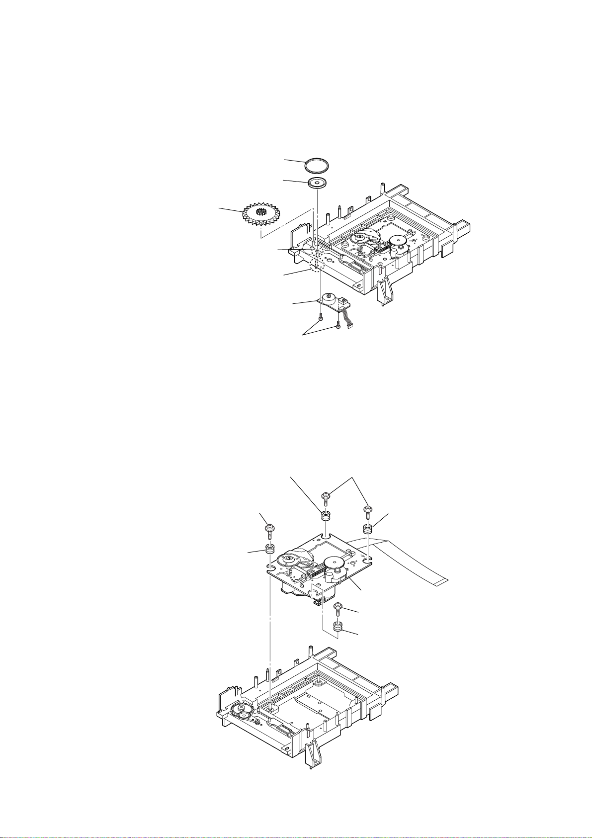
3-8. Pick-Up Assy
7
damper rubber
6
2
screw
(2.6
5
two
screws
(D 2.0 × 6)
damper rubber
×
10)
1
two
(2.6
screws
×
10)
8
pick-up assy
3
screw
(2.6
4
damper rubber
5
damper rubbe
×
10)
9
MCE-F808K
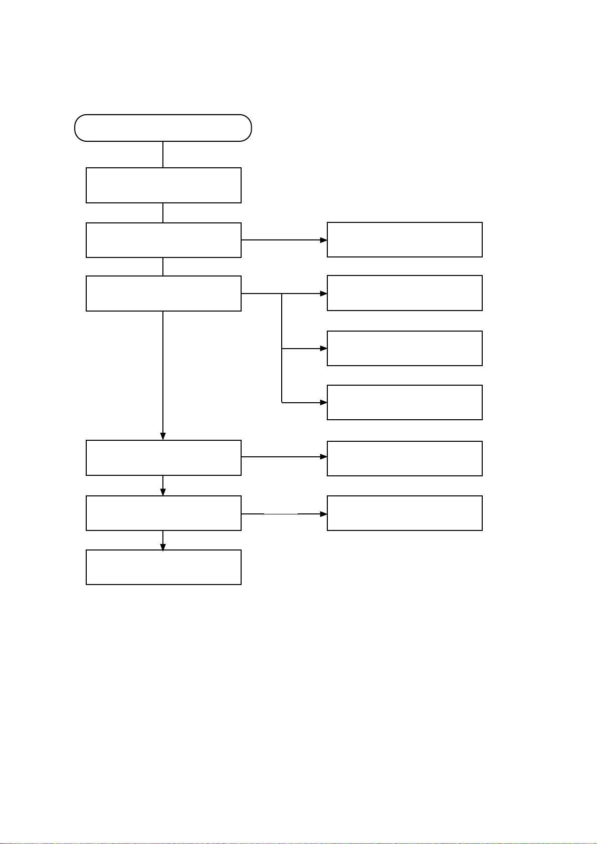
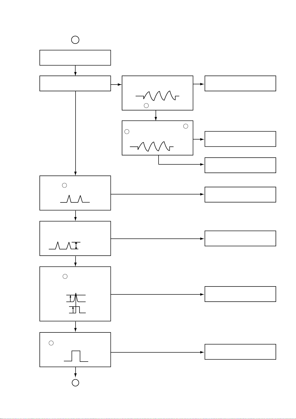
4-1. CD Section
SECTION 4
TROUBLESHOOTING
CD PART
CD Function Select
Is power turned ON?
YES
Does initial reading occur?
YES
Can disc be played?
YES
Is audio output supplied?
NO
Check power supply circuitry.
NO
Check laser circuitry.
Check focusing circuit.
Check disc.
NO
Check tracking servo circuitry.
NO
Check Audio circuitry.
10
YES
OK
• If initial reading is not carried out (with disc)
Does disc motor rotate?
YES
NO
MCE-F808K
Is RF waveform
output?
RFO
IC501 Pin
15
Is tracking servo
NO
operating?
Is the lower envelope of RFO
waveform flat?
YES
Does laser light?
YES
Is signal output at
NO
(TEO)?
1.3V
YES
Is signal output at tracking output
IC503 Pin , ?
PN801 Pin , waveform.
35
14 15
36
YES
NO
Is signal output, at
NO
IC501 Pin ?
YES
NO
(See page 12)
A
(See page 13)
B
• IC501 defective.
16
(FEO)
NO
• Connector
defective.
• Pick-up
defective.
• Pattern defective.
• IC501 or IC502 defective.
Is rotation normal?
Is there any irregularity in
frequency?
YES
Is HF signal normal without
dropout?
YES
Does IC502 Pin (GFS) as
NO
figure?
NO
• Pick-up defective.
• Connector defective.
57
NO
• IC502 defective.
• Disc initial reading damaged or
defective.
• Disc defective.
11
MCE-F808K
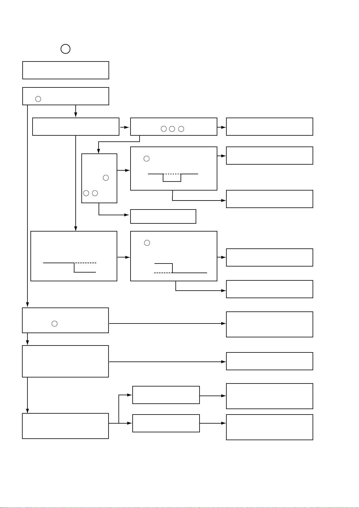
A
When laser does not light.
Is below signal “L” at PN806
10
Pin (LDON)?
YES
NO
Has Pick-up returned to the
innermost position?
YES
Does Voltage
appear at PN
806 Pin
(LOW) & Pins
5
3
, (High)?
NO
Does pick-up stop after having
moved to the innermost position?
PN 803 LMT SW
Are data transferred from
NO
IC301 Pin , , .
94
91
93
YES
Is below signal output at IC503
29
Pin ?
YES
4
YES
NO
• IC301 Defective.
NO
• IC502, 503 defective.
• Slide motor defective.
• Connector defective.
IC301 Defective.
Are detect output input at PN806
9
Pin ?
• LMT SW defective.
• Connector defective.
NO
OPEN
CLOSE
Does fenerate about 2.4V at
IC501 Pin LD?
1
YES
Has laser power source returned
to Q501(Q501 collector voltage
about 1.8V)
YES
Flow laser current?
Both voltage of R501 is about
0.4V?
NO
NO
NO
YES
R501 >> 0.4V
R501 << 0.4V
YES
YES
• IC503 defective.
• IC501 defective.
• Surrounding circuitry defective.
• Connector defective.
• Q501 defective, connector
defective.
• Laser defective.
• Laser defective.
• Connector defective, short etc.
12
B
When laser lights.
MCE-F808K
Do lenses move up and down?
YES
lnsert disc and
in the case of
check of initial
leading.
Is RFO signal waveform output?
IC501 Pin .
15
YES
NO
Is signal output at focus search
terminal?
IC501 pin (FEO)
16
YES
Is signal output at PN801 Pin ,
16
?
YES
NO
NO
• IC501 defective.
• FOCUS Line short.
13
NO
• IC503 defective.
• Actuator short.
• Connecotr short.
• Connector short.
• IC501 defective.
The waveform of RFO is below
figure?
Amplitude
0.7~1.5V
YES
Is FOK signal output?
IC502 Pin .
92
YES
Is FOK signal input to IC301
71
Pin
NO
NO
NO
• Turntable height error.
• Laser diode degraded.
• IC502 defective.
• Pattern defective.
•PN806 defective.
YES
(See page 14)
C
13
MCE-F808K
C
YES
Is RFO signal output?
IC501 Pin .
Is FZC signal output at IC501
Pin ?
(SENSE)
Is MDP signal outut by IC502
Pin ?
16
YES
82
FER
ISTAT
YES
95
• IC501 defective.
NO
• Pick-up defective.
• Connector defective.
NO
• IC502 defective.
When FOK focus
Servo Conform by
FZC signal
YES
Has voltage at disc motor?
at start
YES
NO
NO
• IC502 defective.
• IC501, 502 defective.
• Surrounding circuitry defective.
• Disc Motor defective.
• Connector defective.
14
4-2. MPEG Part Teoubleshooting
Does DC - 33V appear at
PN302 Pin .
END
Dose -33V appear at
ZD704(-)
Check the Q704
TURN ON
Check the -33V (LOW)
of C769(-)
Reper to
Power Circuit
END
YES
YES
YES
NO
NO
NO
28
• MPEG PART
MCE-F808K
1. Is power supplied to MPEG PART IC (2.8V, 5V)
1) 5V : IC801, IC802 pin 81,IC803, IC804
2) 2.8V : IC802 pins 1, 31 ,51
2. NO VIDEO
1) check the 27 MHz (X801)
2) check the MPEG RESET
- IC 801 pin 13, 24, IC802 pin 29
3) check the communication line [FRONT MICOM (IC301) MPEG
(IC802)]
- DATA, ACK, STROBE (IC802 pin 45, 46, 47)
4) check the CLOCK & DATA [DSP(IC502) MPEG (IC802)]
- LRCK, BCK, DATA (IC802 pin 96, 97, 98)
5) check the DATA communication
- check the DATA & CLOCK LINE (IC801, 802, 803, 804)
6) check the VIDEO signal of the IC801 pin 64
- check the normal voltage (IC 801 pin 52, 54, 55, 65)
7) check the COLOR & OSD
- check the DATA (IC801 pin 79, 80, 82, 84)
• P-SENS PART
Does 5V appear at ZD703?
NO
Check the waveform
YES
Check the pattern of
IC301 Pin .
11
Check the R768 and
replace ZD703.
3. NO AUDIO
1) check the 16.9344MHz (X531)
2) check the CLOCK & DATA of DSP (IC 502)
- LRCK, BSK, DATA (IC502 pin 47, 48, 49)
3) check the AUDIO signal (IC801 pin 45, 46, 47, 48)
4) check the Vcc input of IC806 (OPAMP)
5) check the power on of MUTE part
- check the Q801, 802
4. miscellaneous
1) check the communication line between IC802 pin 48, 52, 54
and FRONT MICOM
2) check the MIC input to IC801 Pin 49, 50
of D703 (+).
YES
NO
Replace the D703
• VKK PART
15
MCE-F808K
• Power Circuit (Power Circuit)
Check the Fuse
YES
NO
Replace the Fuse
Check the DC output
of C777(+), C778(-)
YES
Check the DC power
input of IC704
YES
Check the DC power output of
IC703 Pin 6, 24
YES
Check the DC power (12V)
of IC705
YES
Check the 5V of IC706 Pin 2
(CD FUNCTION)
NO
NO
NO
NO
Check the AC output of CN701 Pin 1, 5
YES
Replace the D720
Check the AC output of
CN701 Pin 7, 10
YES
Check or Replace the D708,D709,
D706, D707, D757, D758.
Check or Replace the
D702, D701
Check the “high” of D791(+)
YES
Replace the IC705
NO
Replace the Transformer
NO
Replace the Transformer
NO
Check the Voltage of
IC301 Pin 84
YES
END
• Muting Circuit (MUTE)
Dose “High” appear at Q701,
Q751, Q251, Q201, “B”
YES
check the “Low” of Q701,
Q751, Q251, “C”
YES
NO
NO
NO
Check the “high” of D792(+)
YES
Replace the IC706
Refer to “IC 203 Troubleshooting
(ONLY Q201/251)
Check the “high” of the Q702
“E” (ONLY Q701/751)
YES
Replace the Q702
NO
NO
Refer to IC203, IC552,
Troubleshooting
Refer to IC 301
Troubleshooting
16
MUTE
 Loading...