

Sony MCECX-80-K Service manual
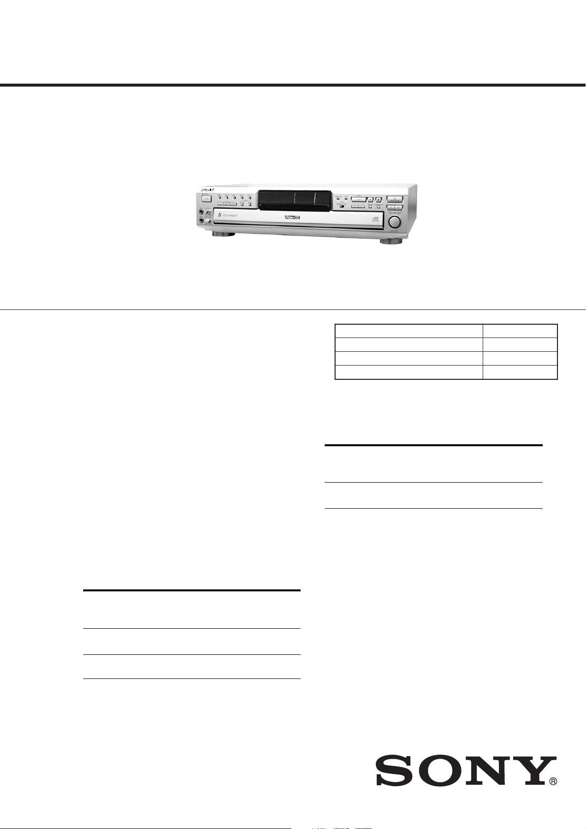
MCE-CX80K
SERVICE MANUAL
E Model
Model Name Using Similar Mechanism NEW
CD Mechanism Type CDM59-5BD24
Base Unit Name BU-5BD24
Optical Pick-up Name KSS-213B/S-N
VIDEO CD player
Laser Semiconductor laser (λ=780nm)
Laser output MAX 44.6 µ W
Wavelength 780 - 790 nm
Signal format system NTSC, PAL
Frequency response 20 Hz to 20 kHz ±1.0 dB
Outputs
Jack
type
AUDIO OUT Phono
VIDEO
OUT
jacks
Phono
jack
Emission duration: continuous
* This output is the value measured at
a distance of 200 mm from the
objective lens surface on the Optical
Pick-up Block with 7 mm aperture.
Maximum
output
level
1.43 V
(at 50 kilohms)
1 Vp-p 75 ohms, unbalanced,
Load impedance
Over 10 kilohms
sync negative
SPECIFICATIONS
Inputs
MIC 1,
MIC 2
General
Power requirements 110 - 120 V or 220 - 240 V AC,
Power consumption 24 W
Dimensions (approx.) 430 110 398 mm
(w/h/d) incl. projecting parts
Mass (approx.) 5.3 kg
Supplied accessories
Audio and video connecting cord (1)
Remote commander (remote) RMT-C98V (1)
Sony R6 (size AA) batteries (2)
Design and specifications are subject to change without notice.
Jack
type
Phone
jack
Maximum
input
level
100 mVp-p 600 ohms
adjustable, 50/60 Hz
Load impedance
VIDEO CD PLAYER
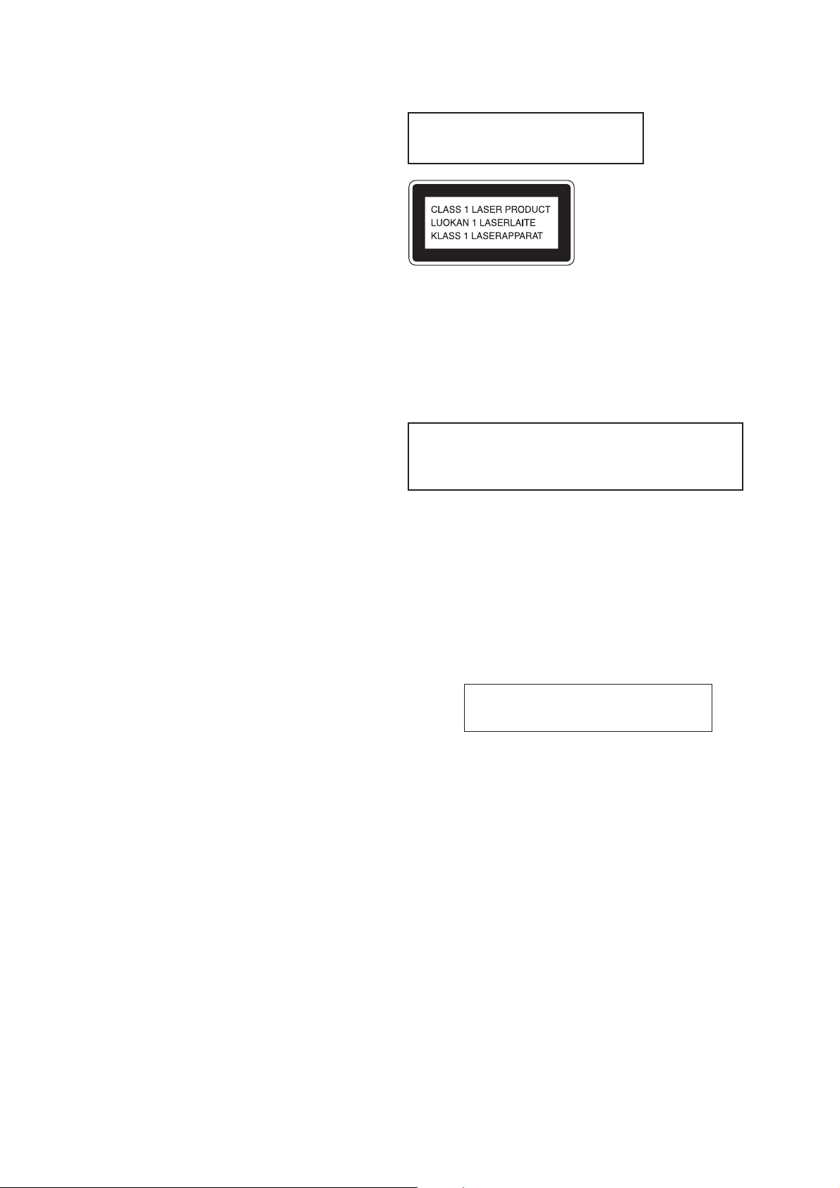
TABLE OF CONTENTS
1. SERVICING NOTES ······················································ 3
2. TEST MODE······································································4
3. GENERAL ·········································································· 6
4. DISASSEMBLY
4-1. UPPER CASE, BOTTOM PLATE, FRONT PANEL········ 7
4-2. BACK PANEL AND DISC TABLE ··································7
4-3. DISP, SWI, VOL AND KARAOKE MIC BOARDS········· 8
4-4. CD MECHANISM DECK (CDM59-5BD24) ··················· 8
4-5. JACK, VIDEO AND MAIN BOARDS ·····························9
4-6. BASE UNIT (BU-5BD24)················································· 9
4-7. T ABLE ASS’Y ································································ 10
4-8. TRAY, BELT (ROTARY) AND SENSOR BOARD ········10
4-9. BELT (LOADING)
AND LOADING MOTOR BOARD································ 11
4-10. ADJUSTING PHASE OF
SWING GEAR AND GEAR (U/D) ································ 12
5. ELECTRICAL ADJUSTMENTS
CD Section ··········································································· 13
6. DIAGRAMS
6-1. Block Diagrams
• Servo Section ································································ 14
• Audio/Video Section ····················································· 15
• Disp/Key Control/ Power Supply Section····················· 16
6-2. Circuit Boards Location··················································· 17
6-3. Printed Wiring Board – Video Section –·························· 21
6-4. Schematic Diagram – Video Section (1/2) –··················· 22
6-5. Schematic Diagram – Video Section (2/2) –··················· 23
6-6. Schematic Diagram – BD Section – ································ 24
6-7. Printed Wiring Board – BD Section – ····························· 25
6-8. Schematic Diagram – Main Section – ····························· 26
6-9. Printed Wiring Board – Main Section –··························· 27
6-10. Schematic Diagram – Disp Section – ······························ 28
6-11. Printed Wiring Board – Disp Section – ···························29
6-12. Printed W iring Board
– JUNCTION/LOADING/MOTOR Section – ················ 30
6-13. Schematic Diagram
– JUNCTION/LOADING/MOTOR Section – ················ 31
6-14. IC Block Diagrams ·························································· 32
6-15. IC Pin Function Descriptions···········································34
Laser component in this product is capable
of emitting radiation exceeding the limit for
Class 1.
This appliance is classified as a CLASS 1 LASER product. The
CLASS 1 LASER PRODUCT MARKING is located on the rear
exterior.
The following caution label is located inside the unit.
CAUTION
Use of controls or adjustments or performance of procedures
other than those specified herein may result in hazardous radiation
exposure.
Notes on chip component replacement
• Never reuse a disconnected chip component.
• Notice that the minus side of a tantalum capacitor may be damaged by heat.
The components identified by mark 0 or dotted
line with mark 0 are critical for safety.
Replace only with part number specified.
7. EXPLODED VIEWS
7-1. CASE SECTION ····························································· 40
7-2. FRONT PANEL SECTION ············································· 41
7-3. CHASSIS SECTION ······················································· 42
7-4. CD MECHANISM DECK SECTION-1
(CDM59-5BD24)····························································· 43
7-5. CD MECHANISM DECK SECTION-2
(CDM59-5BD24)····························································· 44
7-6. BASE UNIT SECTION (BU-5BD24)····························· 45
8. ELECTRICAL PARTS LIST····································· 46
2
SAFETY-RELATED COMPONENT WARNING!!
COMPONENTS IDENTIFIED BY MARK 0 OR DOTTED LINE WITH
MARK 0 ON THE SCHEMATIC DIAGRAMS AND IN THE PARTS
LIST ARE CRITICAL TO SAFE OPERATION. REPLACE THESE
COMPONENTS WITH SONY PARTS WHOSE PART NUMBERS
APPEAR AS SHOWN IN THIS MANUAL OR IN SUPPLEMENTS
PUBLISHED BY SONY.
SECTION 1
SERVICING NOTES
NOTES ON HANDLING THE OPTICAL PICK-UP
BLOCK OR BASE UNIT
The laser diode in the optical pick-up block may suffer electrostatic
break-down because of the potential difference generated by the
charged electrostatic load, etc. on clothing and the human body.
During repair, pay attention to electrostatic break-down and also
use the procedure in the printed matter which is included in the
repair parts.
The flexible board is easily damaged and should be handled with
care.
NOTES ON LASER DIODE EMISSION CHECK
The laser beam on this model is concentrated so as to be focused on
the disc reflective surface by the objective lens in the optical pickup block. Therefore, when checking the laser diode emission,
observe from more than 30 cm away from the objective lens.
LASER DIODE AND FOCUS SEARCH OPERATION
CHECK
Carry out the “S curve check” in “CD section adjustment” and check
that the S curve waveform is output repeatedly.
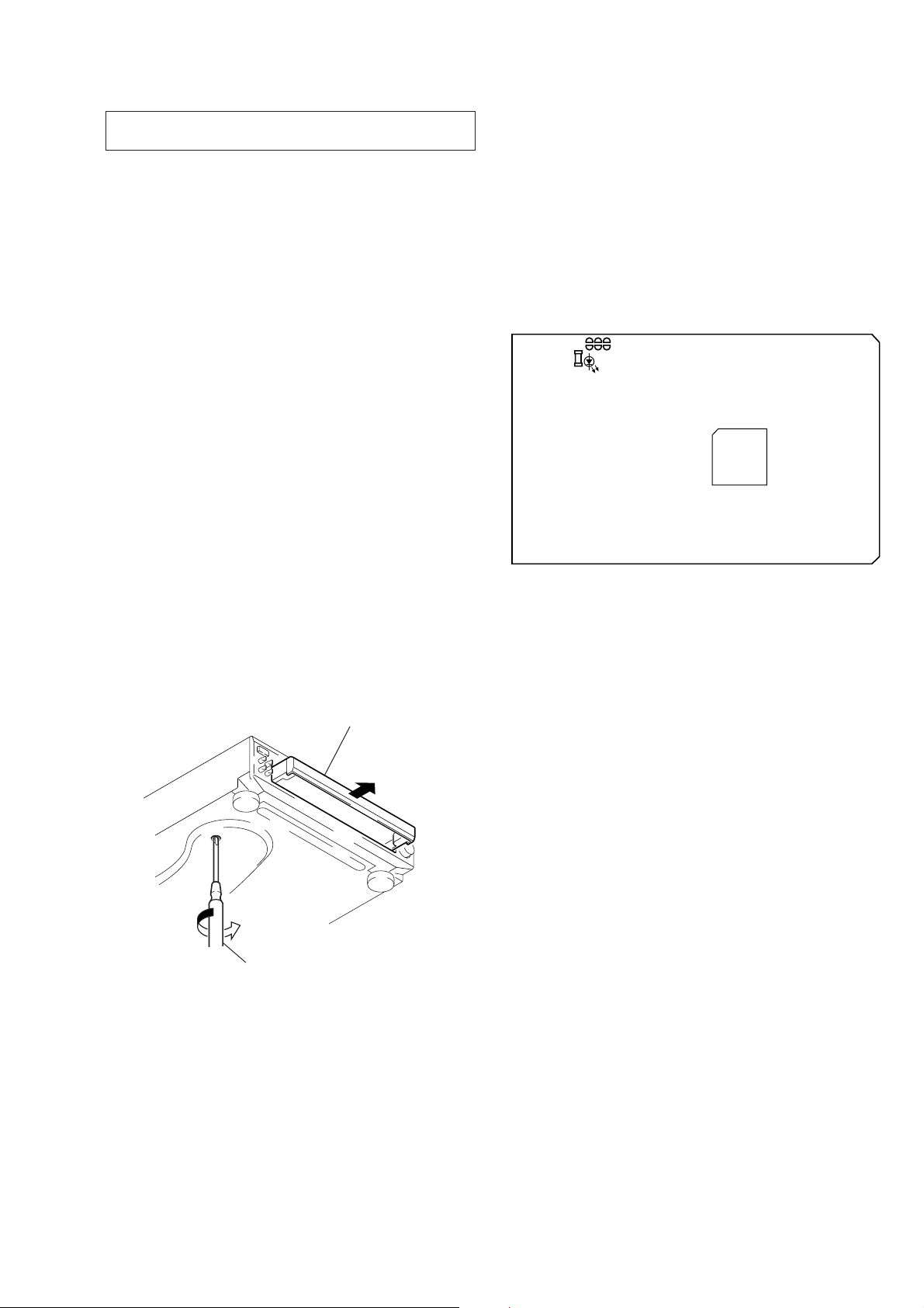
HOW TO OPEN THE DISC TRAY WHEN POWER SWITCH
TURNS OFF
Insert a tapeing driver into the aperture of the unit bottom, and turn
in the direction of arrow (to OUT direction).
* To close the disc table, turn the driver in the reverse direction
(to IN direction).
SELF-DIAGNOSIS
This unit is equipped with a self-diagnosis function.
The function is used for diagnosing the conditions of the circuits of
the VIDEO board.
The circuits can be determined if normal or abnormal by the lighting
of D502 on the VIDEO board.
Lighting of D502
When lit : Operates normally
Blinks repeatedly : The circuit may be faulty.
[VIDEO Board] (Side B)
D502
IC505
The following extension cable is required to check and adjust the
VIDEO board.
J-2501-155-A CN601/MAIN ↔ CN451/VIDEO
J-2501-156-A CN906/MAIN ↔ CN453/VIDEO
J-2501-157-A CN101/BD ↔ CN501/VIDEO
table
tapering driver
* To close the disc table, turn the tapering
driver in the reverse direction (to IN direction).
3
SECTION 2
TEST MODE
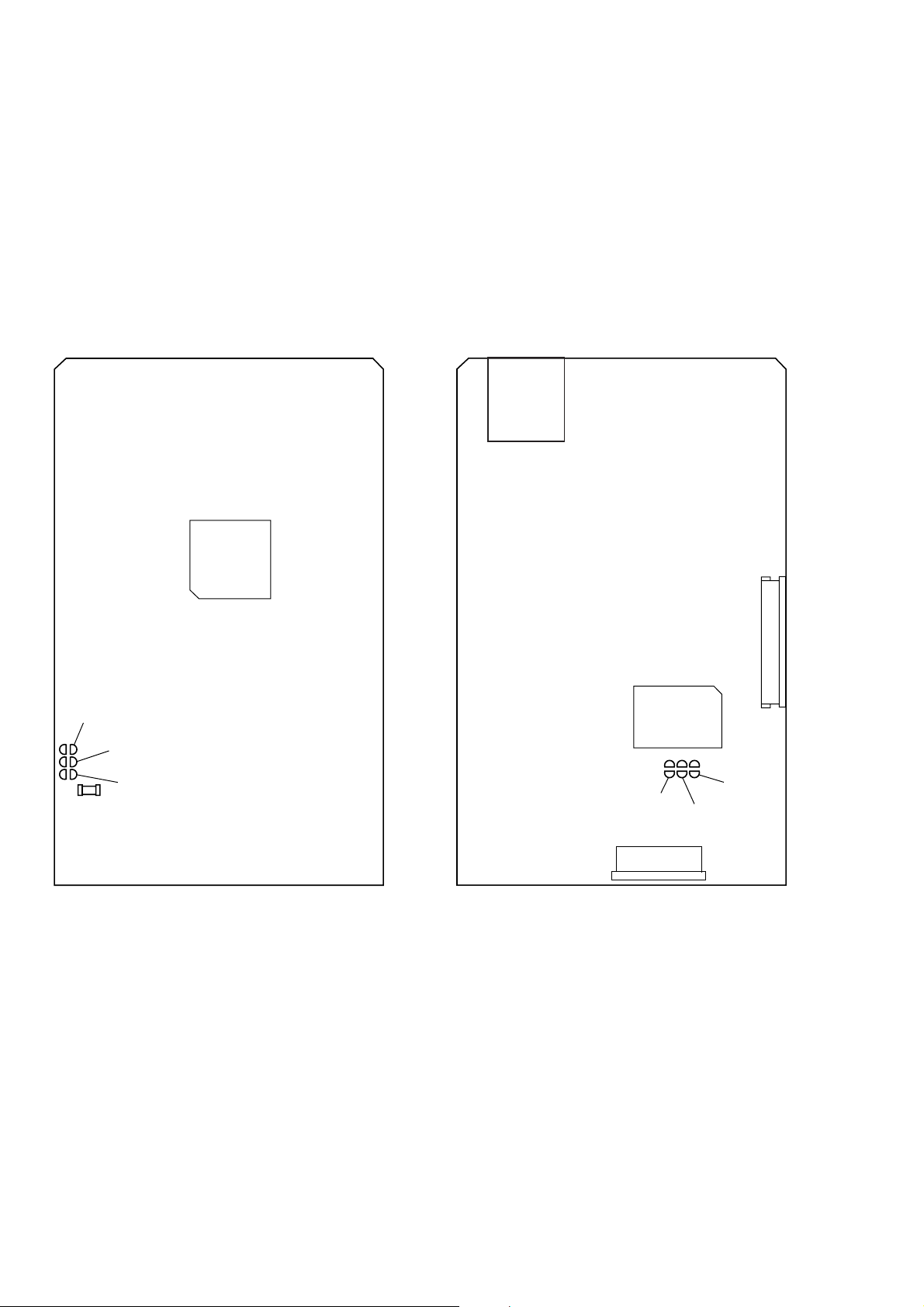
[VIDEO CD Color-bars Mode]
On this mode, the data of the color-bars signal as a picture signal and the 1 kHz sine wave signal as a sound signal are output by the
mechanism controller (IC502) for the video CD signal check. When measurement of the voltage and waveform on the VIDEO board,
perform it in this mode.
For reference, the color-bars signal can be observed at J302/JACK board (VIDEO OUT) and the sound signal can be observed at CNJ151/
MAIN board (AUDIO OUT) using an oscilloscope.
Procedure:
1. Connect the lead wire to both ends of the land of SL503 on the VIDEO board.
2. Turn the power on.
3. After 2 or 3 seconds later, connect the lead wire.
4. After measuring, remove the lead wire connected.
[VIDEO Board] (Side B)
SL503
SL502
[VIDEO Board] (Side A)
CN302
IC505
CN501
IC502
D502
SL501
SL503
CN503
SL501
SL502
4
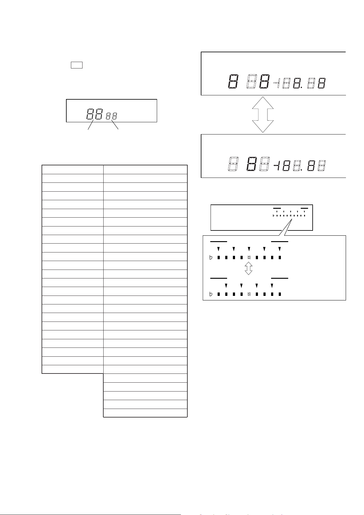
[Fluorescent Indicator Tube and Key Check Mode]
r
Light alternately
KEY CONTROL
#
KEY CONTROL
Light alternately
#
KEY CONTROL
#
1. Short-circuit the SL501 on the VIDEO board.
2. Press the 1/u button to turn ON the power.
The whole fluorescent indicator tube light up.
3. All buttons have individual button numbers.
When a button is pressed, the button number is counted up and
displayed.
Count up display Display button numbe
4. To exit the mode, disconnect the power code from the outlet.
Buttons and Corresponding Button Numbers
Button Button Number or Display
1/u 15
KARAOKE PON 77
§ OPEN/CLOSE 16
PICTURE 49
SOUND 5d
· (PLAY) SELECT Partial lighting 1
P (PAUSE) Partial lighting 2
p (STOP) All lit
PREV 30
NEXT 31
RETERN 0E
˜ 6C
NATURAL 67
n 6b
DISC1 40
DISC2 41
DISC3 42
DISC4 43
DISC5 44
JOG SELECTOR (button) 81
JOG SELECTOR (knob) When roatated colck wise:
DISC SKIP The key control indicators
EX-CHANGE light up from left to right.
When rotated counter colck wise:
The key control indicators
light up from right to left.
3E
3F
Partial lighting 1
Partial lighting 2
5
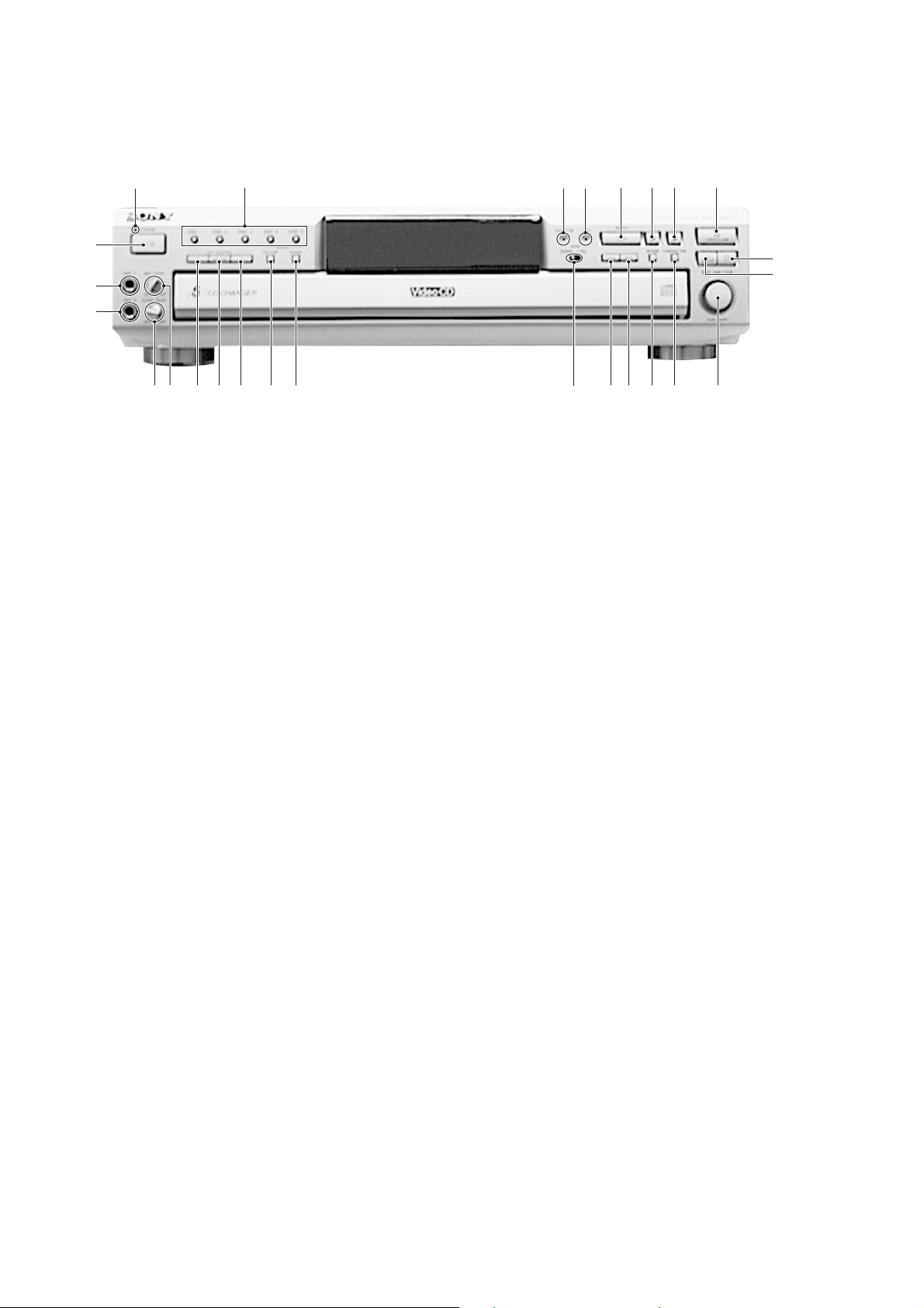
SECTION 3
GENERAL
wh
wg
wf
1
2
1 STANDBY indicator
2 DISC 1-5 buttons
3 KARAOKE PON indicator
4 2 DISC indicator
5 G SELECT button
6 P button
7 x button
8 A OPEN/CLOSE button
9 DISC SKIP button
q; EX-CHANGE button
qa l AMS L knob
qs KARAOKE PON button
qd RETERN button
3 4
5 6 7 8
qh
qf NEXT button
qg PREV button
qh MODE knob
qj EFFECT SOUND button
qk EFFECT PICTURE button
ql KEY CONTROL # button
w; KEY CONTROL NATURAL button
wa KEY CONTROL 2 button
ws MIC LEVEL knob
wd ECHO LEVEL knob
wf MIC2 jack
wg MIC1 jack
wh 1/u (POWER) button
9
q;
!¡qsqdqfqgqjqkqlw;wawd ws
6
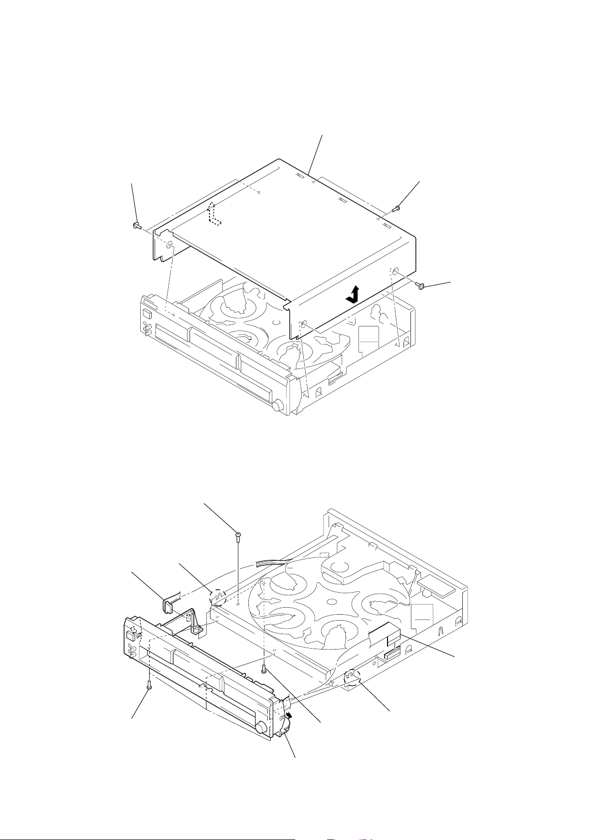
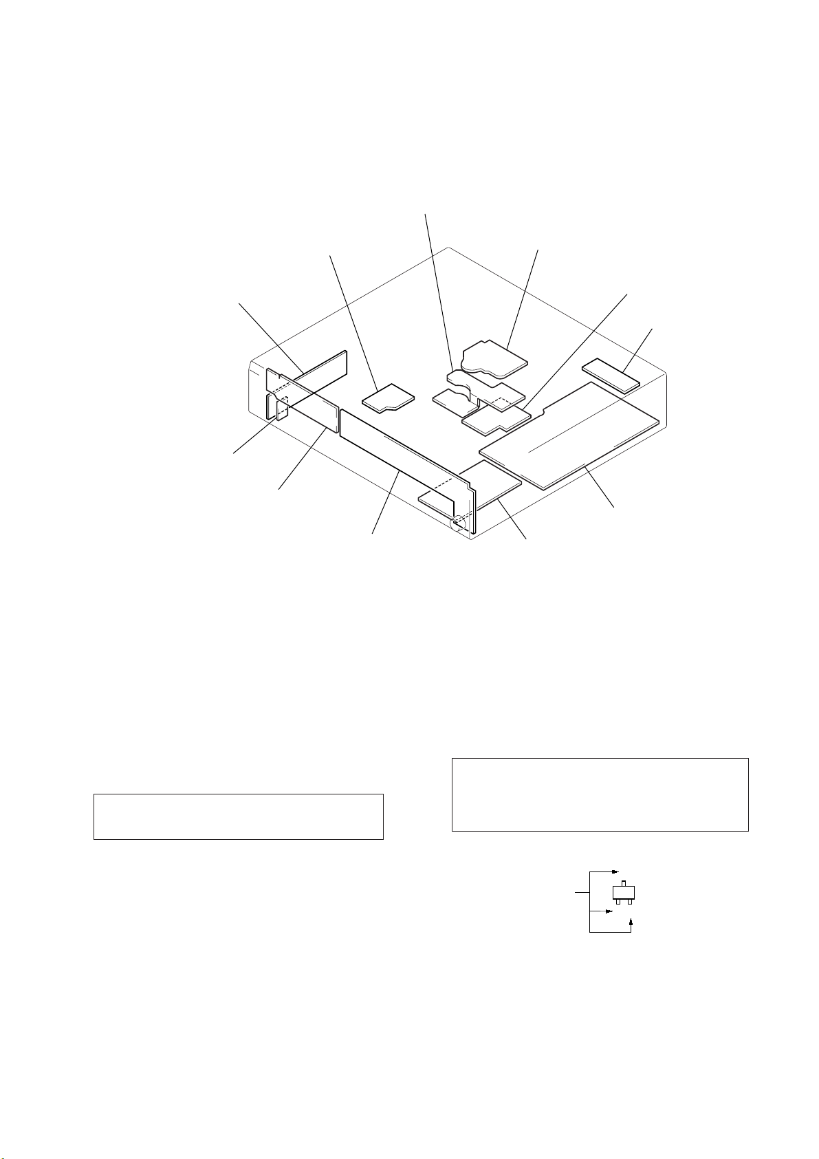
SECTION 4
)
2
Connector
(CN702)
Claw
5
Three screws
(BVTP3
×
8)
4
Screw
(BVTP3
×
8)
3
Screw (BVTP3 × 8)
6
Front panel section
Claw
1
Wire (flat type) (19 core)
(CN801)
DISASSEMBLY
Note : Follow the disassembly procedure in the numerical order given.
4-1. UPPER CASE, BOTTOM PLATE, FRONT PANEL
4
2
Two screws
(case3 TP2)
Cover (409537)
3
Two screws
(BVTP3
×
8)
1
Two screws
(case3 TP2
4-2. BACK PANEL AND DISC TABLE
7
4-3. DISP, SWI, VOL AND KARAOKE MIC BOARDS
)
qd
Two screws
qj
KARAOKE MIC board
qg
Two accessory plates
9
Two knob VOL
0
Two nuts
(BVTP3
qh
jack
×
Holder
8)
qa
qf
Holder (PHONE PWB)
8
7
Connector
(CN701)
VOL board
6
Two screws
(BVTP3
×
8)
qs
Connector (CN702)
3
Ten screws
(BVTP3
SWI board
5
DISP board
4
Wire (flat type) (19 core)
(CN810)
×
8)
2
Ring spring (SUS)
1
Knob (AMS)
4-4. CD MECHANISM DECK (CDM59-5BD24)
3
Three screws
(BVTP3 × 8)
5
Screw
(BVTP3 × 8)
a
qs
CD mechanism deck
(CDM59-5BD24)
qa
Wire (flat type) (21 core)
(CN101)
0
Connector
(CN600)
2
Three screws
(BVTP3 × 8)
4
Slide the tray until the screw
that fixes the table assy can be
seen through around hole
in the table assy.
a
1
6
9
Connector (Power cord
(CN901)
8
Connector
(CN907)
7
Connector
(CNP602)
Insert a tapering driver from the bottom of the chassis,
and turn it in the direction of the arrow until the base unit
goes down to the lowest position.
8
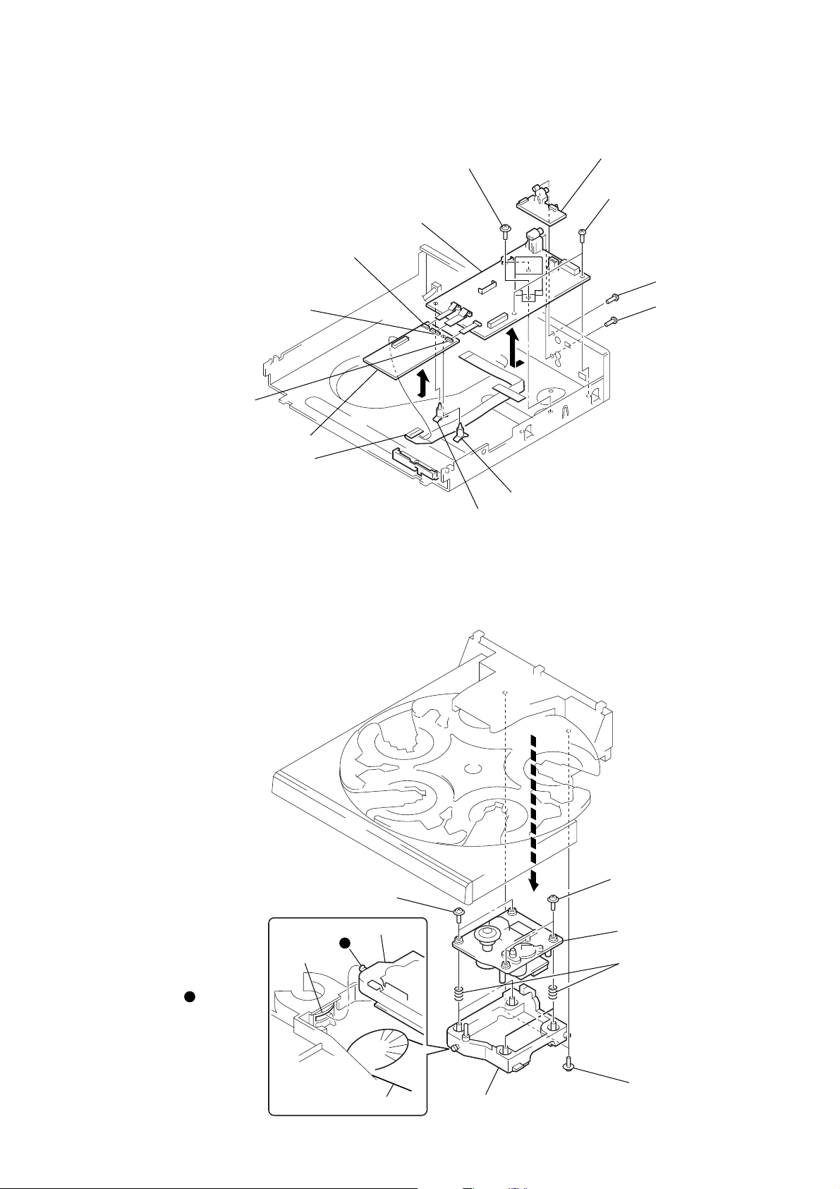
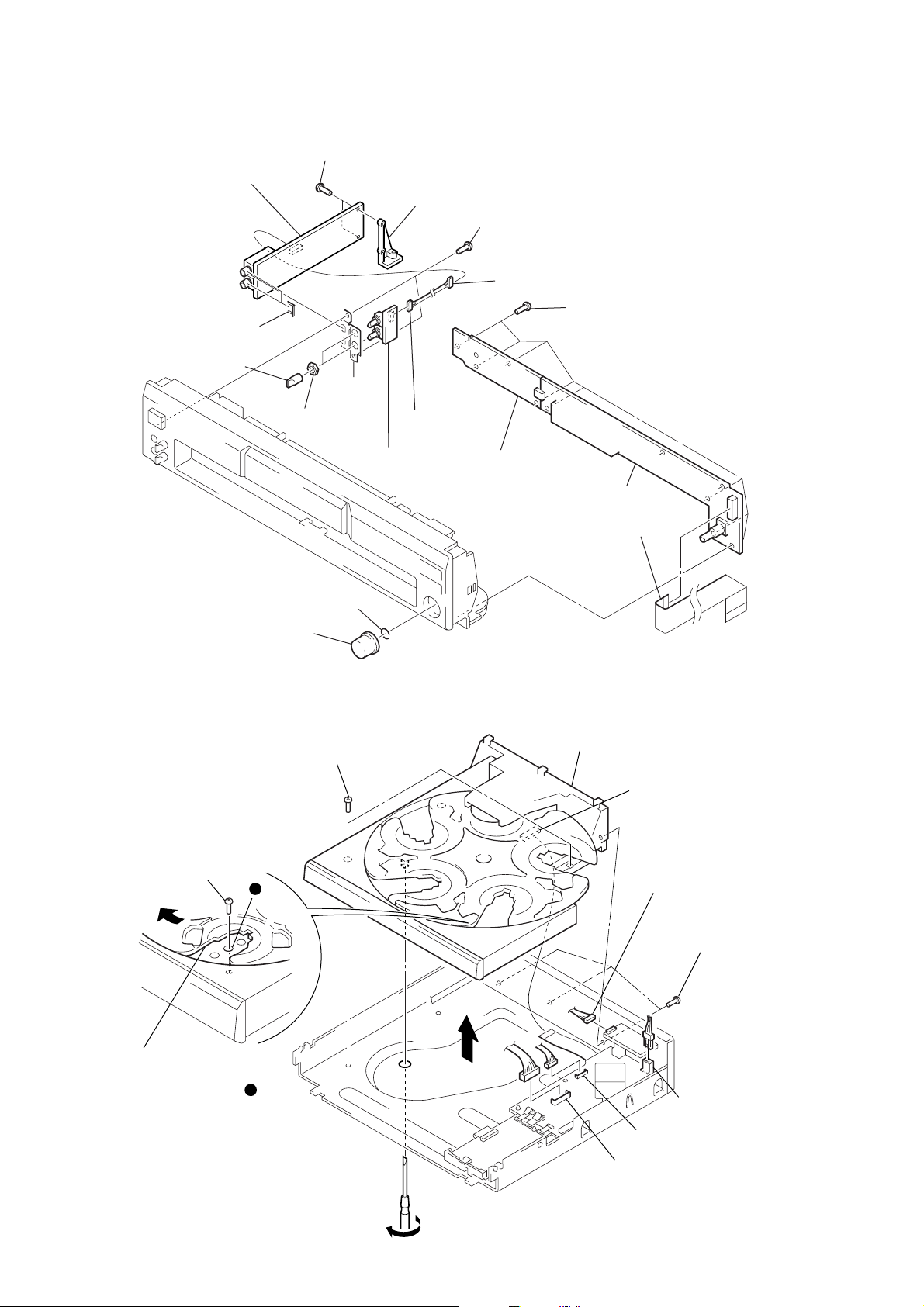
4-5. JACK, VIDEO AND MAIN BOARDS
)
)
4
Two screws
(PTPWH M2.6)
5
Two screws
(PTPWH M2.6)
6
Base unit (BU-5BD24)
7
Four compression springs (932)
2
1
Two screws
(PTPWH M2.6)
3
Holder (BU) assy
Lever (lifter)
BU section
Note: When installing the BU
on the chassis, set the
lever (lifter) in free
position, the gear (U/D)
in UP position, and insert
the shaft into the
groove of gear (U/D).
Gear (U/D)
b
b
1
Wire (flat type)
(9 core) (CN451)
2
Wire (flat type)
(13 core) (CN503)
3
Wire (flat type)
(17 core) (CN453)
6
VIDEO board
4
Wire (flat type)
(23 core) (CN501)
qd
MAIN board
qa
Two screws
(PTTWH3
×
6)
5
qs
PC board holder
9
PC board holder
JACK board
0
Two screws
(BVTP3
×
7
8
8)
Screw
(BVTP3
Screw
(BVTP3
×
8
×
8
4-6. BASE UNIT (BU-5BD24)
9
4-7. TABLE ASS’Y
5
Table assy
Note: When installing the table assy
on the chassis assy, engage
the gear (loading C) with the groove
by looking into the gear through
a hole in the table assy.
e
q;
Three screws
(BTTP M2.6)
e
qa
Clamp
3
qs
Bracket (guide)
Gear
(loading C)
2
c
Two screws
(BTTP M2.6)
d
8
Two screws
(BTTP M2.6)
9
Bracket (guide 2)
4
Wire (flat type)
(6 core) (CN15)
6
Screw
(BTTP M2.6)
7
Bracket (guide)
1
Slide the tray until the screw
that fixes the bracket (guide)
can be seen through a round
c
hole , in the table assy.
d
4-8. TRAY, BELT (ROTARY) AND SENSOR BOARD
1
Screw
(PTPWH M2.6)
2
Tray
6
SENSOR board
3
Belt (rotary)
10
4
Two screws
(BTTP M2.6)
5
Two screws
(BTTP M2.6)
4-9. BELT (LOADING) AND LOADING MOTOR BOARD
4
LOADING MOTOR board
1
Belt (loading)
3
Two screws
(BTTP M2.6)
2
Connector
(CN13)
11
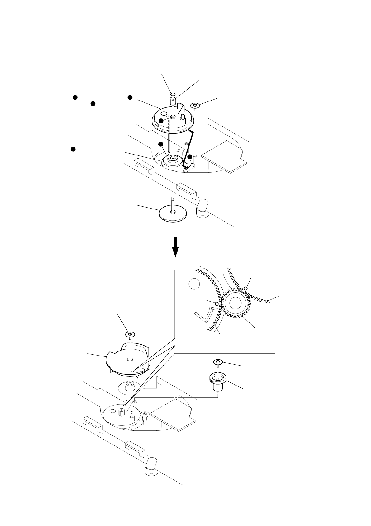
4-10. ADJUSTING PHASE OF SWING GEAR AND GEAR (U/D)
h
5
Stopper washer (FR)
3
Let the swing gear through under the
chassis and engage its dowel
with the groove of rotary encoder.
2
Install the rotary encoder so that
its groove comes to the position
shown in the figure.
h
f
f
1
Insert the shaft gear up to the
position where its shaft comes
out by 5 mm.
g
g
f
h
4
Push fully the shaft of shaft gear and
align the hole shape of gear (loading B).
6
Screw
(PTPWH M2.6)
7
Gear (U/D)
8
Screw
(PTPWH M2.6)
Circle mark
Swing gear
Fig. A
Circle mark
Gear (U/D)
Gear (RV)
q;
Screw
(PTPWH M2.6)
9
Gear (RV)
Note: Align swing gear, a circle mark
on the gear (U/D), and the teet
of gear (RV) to the position
showing in the Fig. A.
12
SECTION 5
e
)
r
ELECTRICAL ADJUSTMENTS
CD SECTION
Notes:
1. CD block basically constructed to operate without adjustment.
Therefore, check each item in order given.
2. Use YEDS-18 disc (Part No.: 3-702-101-01) unless otherwise
indicated.
3. Use the oscilloscope with more than 10 MΩ impedance.
4. Clean an object lens by an applicator with neutral detergent
when the signal level is low than specified value with the
following checks.
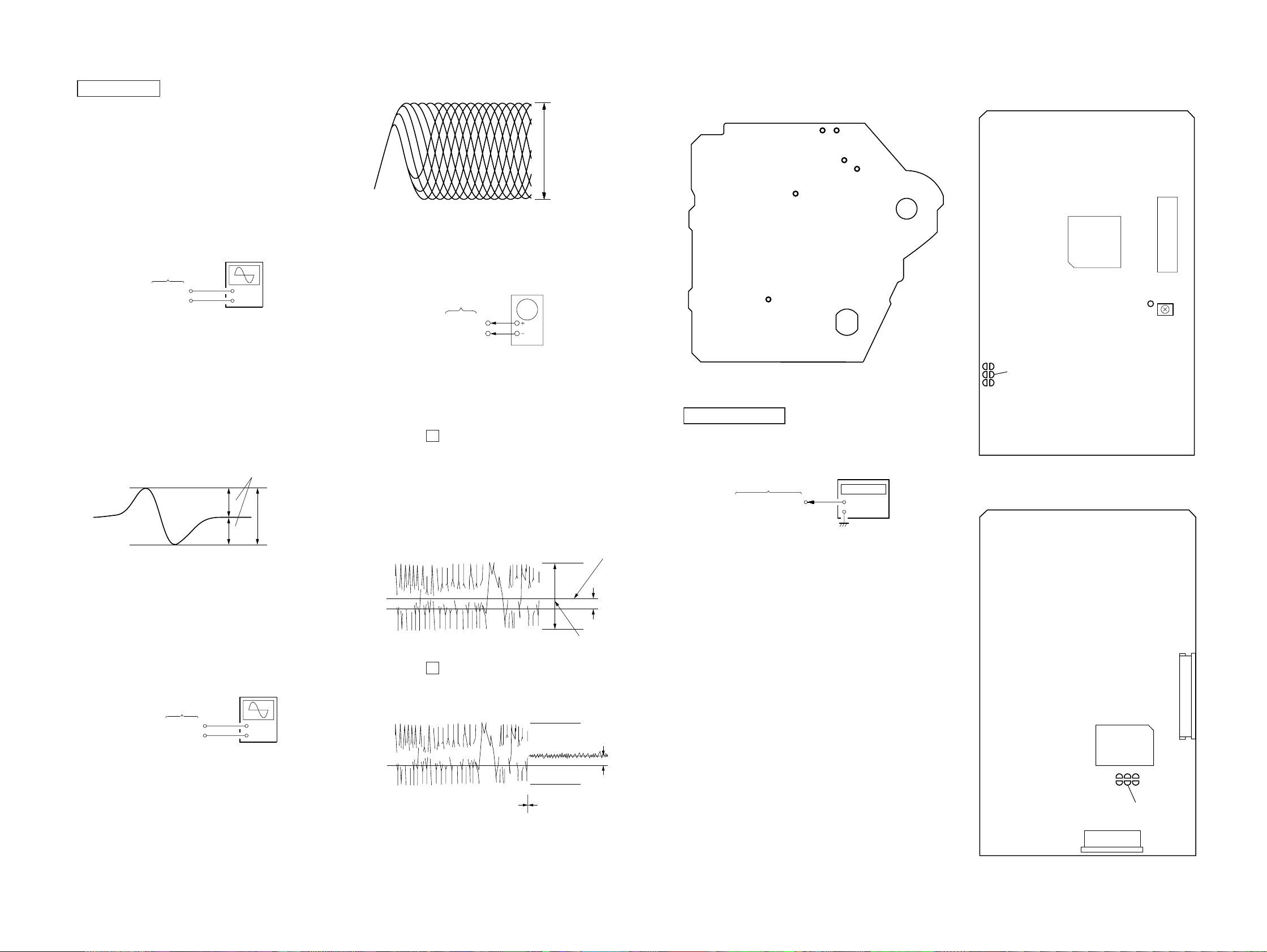
S-Curve Check
Connection:
oscilloscope
BD board
TP (FE)
TP (VC)
Procedure:
1. Connect the oscilloscope to TP (FE) and TP (VC) on BD board.
2. Connect between test point TP (FEI) and TP (VC) by lead wire.
3. Push power switch on.
4. Put disc (YEDS-18) in and push power switch on again and
actuate the focus search. (actuate the focus search when disc
table is moving in and out.)
5. Confirm that the oscilloscope waveform (S-curve) is
symmetrical between A and B. And confirm peak to peak level
within 3.0 ± 1.0 Vp-p.
S-curve waveform
6. After check, remove the lead wire connected in step 2.
Note: • Try to measure several times to mak e sure that the ratio of A : B
or B : A is more than 10 : 7.
• Take sweep time as long as possible and light up the brightness
to obtain best waveform.
RF Level Check
Connection:
BD board
TP (RF)
TP (VC)
Procedure:
1. Connect the oscilloscope to TP (RF) and TP (VC) on BD board.
2. Push power switch on.
3. Put disc (YEDS-18) in and play.
4. Confirm that the oscilloscope waveform is clear and check RF
signal level is correct or not.
Note: Clear RF signal waveform means that the sha pe “” can be clearly
distinguished at the center of the waveform.
+
–
symmetry
A
within 3.0
B
oscilloscope
(AC range)
+
–
±
1.0 Vp-p
RF signal waveform
VOLT/DIV: 200 mV
TIME/DIV: 500 ns
(with the 10: 1 probe
in use)
level: 1.3 Vp-p
+0.25
–0.20
When observing the eye pattern, set the oscilloscope for AC range
and raise vertical sensitivity.
E-F Balance Check
oscilloscop
BD board
TP(TE)
TP(VC)
Procedure :
1. Connect oscilloscope to test point TP (TE) and TP (VC) on BD
board.
2. Short-circuit the SL502 of the VIDEO board.
3. Push the Power switch on to set the ADJ mode.
4. Put disc (YEDS-18) in to play the number five track.
5. Press the G button. (The tracking servo and the sledding servo
are turned OFF.)
6. Check the level B of the oscilloscope’s waveform and the A
(DC voltage) of the center of the Traverse waveform.
Confirm the following :
A/B × 100 = less than ± 22%
Traverse waveform
VOLT/DIV : 500mV (10 : 1 probe)
TIME/DIV : 10ms
Center of the waveform
B
0V
level : 1.3 ± 0.6 Vp-p
A (DC voltage
7. Press the G button. (The tracking servo and sledding servo are
turned ON.) Confirm the C (DC voltage) is almost equal to the
A (DC voltage) is step 7.
Traverse waveform
C (DC
0V
Tracking servo
Sledding servo
OFF
Tracking servo
Sledding servo
ON
voltage)
8. Desolder the shortland short-circuited at step 2.
Adjustment Location:
[BD BOARD] (SIDE B)
TP
(FE)
TP
(VC)
TP
(FEI)
TP
(RF)
TP
(TE)
TP
(FOK)
VIDEO SECTION
Frequency Adjustment
Connection:
VIDEO board
TP508 (27 MHz)
Procedure:
1. Connect the frequency counter to TP508 (27 MHz) on VIDEO
board.
2. Color system switch (S501) on the JA CK board select to NTSC
and push the power switch on.
3. Adjust CT503 on the VIDEO board so that the frequency counter
reading 27.0 MHz ± 80 Hz at stop status.
frequency counte
+
–
Adjustment Location:
[VIDEO BOARD] (Side B)
SL502
[VIDEO BOARD] (Side A)
IC505
IC502
CN503
TP508
(27 MHz)
SL502
IC507
CT503
VIDEO
Frequency
Adjustment
CN501
1313
MCE-CX80K
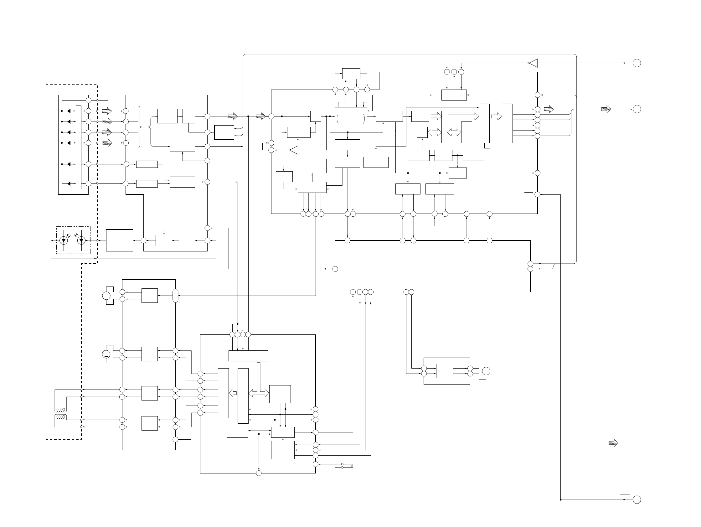
6-1. BLOCK DIAGRAM
— SERVO SECTION —
DETECTOR
A
B
C
D
F
E
OPTICAL PICK-UP
(KSS-213B/S-N)
LASER DIODE
PD
7
4
2
1
5
I-V AMP
10
6
LD
(SPINDLE)
M101
A+5V
AUTOMATIC
M
A
3
B
4
C
5
D
6
F
8
F I-V AMP
E
9
E I-V AMP
POWER
CONTROL
Q101
FOCUS/TRACKING COIL DRIVE,
SPINDLE/SLED MOTOR DRIVE
OUT+
27
OUT–
26
SECTION 6
DIAGRAMS
RF AMP,
FOCUS/TRACKING ERROR AMP
1
LD
IC102
MOTOR
DRIVE
IC103
RF
SUMMING
AMP
APC LD
AMP
FOCUS
ERROR AMP
TRACKING
ERROR AMP
APC PD
AMP
IN+, IN–
23, 24
RF EQ
AMP
RFO
RFE
FE BIAS
LDON
IC104
6320
VCKI
XTAO
CLOCK
GENERATOR
INTERNAL BUS
DIGITAL
OUT
SBSO
75
62
XTAI
SCLK
ERROR
CORRECTOR
PEAK
DETECTOR
83
2
SENSE CLK
D/A DIGITAL
PROCESSOR
MUTE
79
10
DSP MUTE
XTSL
DATA
BCLK
LRCK
GFS
RFCK
PROCESSOR
C2PO
SERIAL/PARALLEL
DOUT
XRST
CTRL1
11
CTRL2
27
64
46
47
45
54
55
56
71
81
CTL1
DATA
BCK
LRCK
C2PO
CTL1
CTL2
FILTER
32
34
33
MDS
97
31
PCO
FILO
DIGITAL PLL
VARI-PITCH
DOUBLE SPEED
SYNC
PROTECTOR
TIMING
GENERATOR 1
SCOR
74
18
28
LDON
WFCK
73
SCOR
1
CLTV
SENSE
3
FILI
TIMING
GENERATOR 2
DSP LATCH
DSP CLK
DSP DATA
4
5
EFM
DEMODULATOR
ADDRESS
GENERATOR
SUBCODE Q
PROCESSOR
SUBQ
SQCK
77
78
37
36
SUBQ CLK
LOAD IN
50
49
REGISTER
32K
RAM
SUBCODE P – W
PROCESSOR
D+5V
SYSTEM CONTROLLER
SUBQ DATA
IC502 (1/3)
LOAD OUT
PRIORITY
ENCODER
EXCK
76
DIGITAL SIGNAL PROCESSOR
IC101 (1/2)
16
RF EQ
SWITCH
17
Q102, 103
FE
15
14
TE
13
19
PD
2
CTL1
CTL2
RFAC
36
ASYMMETRY
CORRECTOR
ASYI
38
ASYO
39
NOISE
SHAPER
MIX
18-TIMES
OVERSAMPLING
FILTER
CLV
PROCESSOR
MDP
MON
FSW
94
95
96
MCLK
33.8MHz
DATA, BCK,
LRCK, C2PO
A
B
(Page 15)
(Page 15)
(TRACKING)
(FOCUS)
16
2-AXIS
DEVICE
M102
(SLED)
26
29
28
27
FE
TE
SE
RFDC
A/D
CONVERTER
SERVO DSP
FOCUS/TRACKING/SLED
SERVO
INTERFACE
COUT
89
IN–
IN–
IN+
IN–
IN+
MUTE
IN+
9
10
SFDR
100
SRDR
2
4
5
19
20
15
TFDR
4
TRDR
6
FFDR
8
FRDR
10
PWM GENERATOR
FOCUS/TRACKING/SLED
OUT+
13
M
12
2
1
16
17
OUT–
OUT–
OUT+
OUT+
OUT–
MOTOR
DRIVE
COIL
DRIVE
COIL
DRIVE
DIGITAL SERVO
PROCESSOR
IC101 (2/2)
MIRR/DFCT/
FOK
DETECTOR
SERVO AUTO
SEQUENCER
CPU
INTERFACE
FOK
MIRR
DFCT
SENS
DATA
CLOK
XLAT
SSTP
LOADING MOTOR DRIVE
IC11(1/2)
MOTOR
DRIVE
OUT1-
OUT1+
9
8
M
M10
(LOADING)
• SIGNAL PATH
: CD PLAY
RESET
C
(Page 15)
FIN1
3
RIN1
2
93
91
92
80
86
88
87
99
S101
(LIMIT)
A+5V
1414
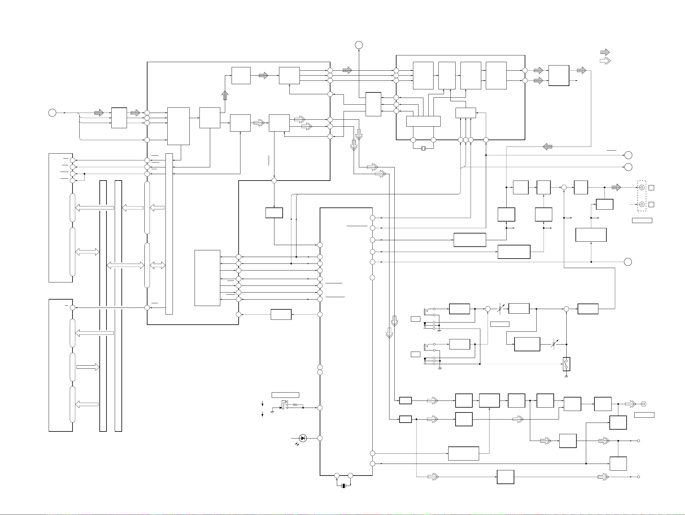
— AUDIO/VIDEO SECTION —
DATA, BCK,
LRCK, C2PO
B
(Page 14)
D-RAM
IC507
PROGRAM ROM
IC506
WE
RAS
UCAS
LCAS
CE
13
14
28
29
A0 – A8
16 – 19, 22 – 26
DATA
BCK
LRCK
C2PO
A0 – A8
D0 – D15
A0 – A10
DATA BUS
LEVEL
SHIFT
IC501
ADDRESS BUS
A0 – A10
D0 – D15
MPEG VIDEO/AUDIO DECODER,
VIDEO SIGNAL PROCESSOR
IC505
CD-DATA
4
CD-BCK
3
CD-LRCK
5
CD-C2PO
6
MWE
38
RAS0
42
CAS
40
58 – 56, 54, 52 – 50, 48, 46 – 4410 – 15, 17, 19, 21, 23 – 29
MCE
3722
MA0 – MA10
MD0 – MD15
CD-ROM
INTERFACE
CIRCUIT
D-RAM/ROM INTERFACE
MPEG
SYSTEM
DECODER
CPU
INTERFACE
HCK
HD-IN
HD-OUT
HSEL
HINT
HRDY
RESET
RREF
MPEG
AUDIO
DECODER
MPEG
VIDEO
DECODER
117
119
112
121
114
113
72
AUDIO
INTERFACE
CIRCUIT
VIDEO
PROCESS
CIRCUIT
PGIO2/VSYNC/CSYNC
93
BUFFER
Q502
DATA
SWITCHING
Q501
CLK
DA-DATA
DA-BCK
DA-LRCK
DA-XCLK
Y-OUT
C-OUT
VCK-IN
45
33
31
32
21
20
23
2460
35
110
111
108
86
69
75
106
BUS
CLK1
DATA1O
DATA1I
CL680 SEL
CL680 HINT
CL680 HRDY
CL680 RESET
XVLEVEL DOWN
(Page 14)
A
MCLK
33.8MHz
DF LATCH
DEVICE RESET
AMP ON
LO BOOST
AUDIO MUTE
MIC CTRL
OSC
BUFFER
IC504
22
77
100
47
48
89
DATA
18
BCK
17
LRCK
19
768FSO
21
384FSO
20
MCKO
4
INPUT
INTERFACE
CIRCUIT
TIMING CONTROL/
CLOCK GENERATOR
XT2
J701
MIC1
X503
27MHz
XT1
DIGITAL FILTER,
D/A CONVERTER
DIGITAL
FILTER,
NOISE
SHAPER
CIRCUIT
IC702 (1/2)
IC509
D/A
CONVERTER
MODE
CONTROL
ML
MC
MD
9 724 1
8
CLK
DATA
AMP ON
SWITCH CONTROL
Q181,182
MIC AMP
LOW-PASS
RSTB
10
+
FILTER
AMP ON
SWITCH
Q151
SWITCH CONTROL
RV701
MIC LEVEL
VOUTL
VOUTR
BOOST
Q183,184
MIX AMP
IC703(1/2)
LINE
AMP
IC151
R-CH
MCE-CX80K
• SIGNAL PATH
: CD PLAY (AUDIO)
: CD PLAY (VIDEO)
14
11
BOOST
AMP
IC152
BOOST
SWITCH
Q152
LOW-PASS
FILTER
IC101
R-CH
+
+
R-CH
LINE
AMP
IC153
R-CH
MUTING CONTROL
IC703 (2/2)
• R-ch is omitted due to
same as L-ch.
DATA, CLK
MUTING
Q153
R-CH
SWITCH
Q905
MIC AMP
RESET
CD POWER
R-CH
C
D
E
(Page 14)
(Page 16)
L
R
J151
AUDIO OUT
(Page 16)
12 – 5, 27, 26, 23
D0 – D7
O0 – O7 A0 – A10 DQ1 – DQ16
13 – 15, 17 – 21 2 – 5, 7 – 10, 31 – 34, 36 – 39
D8 – D14
A11 – A17
25, 4, 28, 29, 3, 2, 30
16
DATA BUS
ADDRESS BUS
NTSC
AUTO
PAL
S501
COLOR SYSTEM
(SELF DIAGNOSIS)
D502
SYSTEM CONTROLLER
94
MUSIC VOL
34
RTS1
93
NT/PAL
TEST LED
73
X501
10MHz
IC502 (2/3)
SHARPNESS
XIN
1315
XOUT
VMUTE
J702
MIC2
B.P.F.
B.P.F.
40
65
MIC AMP
IC702 (2/2)
VIDEO
BUFFER
Q301
VIDEO
BUFFER
Q304
SHARPNESS
CONTROL SWITCH
Q306
SHARPNESS
FILTER
Q302
C
BUFFER
Q303
DIGITAL ECHO
VIDEO
BUFFER
Q307
IC701
VIDEO
BUFFER
Q308
RV703
Y/C MIX
Q310
Y
AMP
Q451
MUTING
Q701
VIDEO
AMP
Q452
VIDEO
MUTE
Q454
Y
MUTE
Q453
J302
VIDEO OUT
Y
C
1515
MCE-CX80K
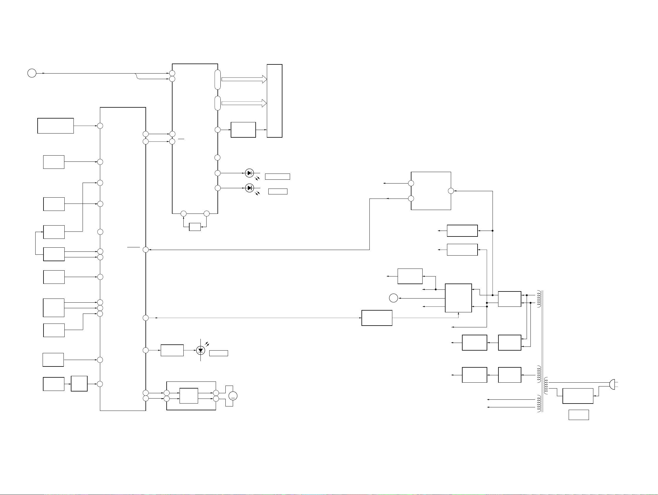
— DISP/KEY CONTROL / POWER SUPPLY SECTION —
(Page 15)
DATA, CLK
D
REMOTE CONTROL
FUNCTION
FUNCTION
FUNCTION
RECEIVER
IC802
S809-814
KEY
S831-836
KEY
S802-808
S837,838
KEY
SYSTEM CONTROLLER
IC502 (3/3)
7
REMOTE IN
KEY1
90
KEY2
91
KEY3
92
KEY4
95
FL CS
FL BLK
79
80
DATA
CLK
FLUORESCENT INDICATOR TUBE DRIVE
64
63
62
61
DI
CL
CE
BLK
59
IC801
OSCI
OSC
C802, R804
S43
S42
S41
58
S1 – S20
C2 – C8
C1
OSCO
56 – 37
3 – 9
2
14
15
16
GRID DRIVE
Q801
FLUORESCENT
INDICATOR TUBE
FL801
D804
KARAOKE PON
D806
2DISC
D+5V (UNSW)
+5V REGULATOR &
RESET SIGNAL GENERATOR
IC903
OUT
5
IN
4
RST
+10V
1
RIPPLE FILTER
Q906
JOG
DIAL
S807
MODE
SWITCH
ROTARY
ENCODER
S11
POSITION
SWITCH
D801
TABLE
SENSOR
D802
DISC
SENSOR
SENS
DRIVE
Q605
12
25
JOG1
26
JOG2
MODE SW
97
ENC1
57
ENC2
58
OUTSW
59
T SENS
6
D SENS
19
16
XRESET
P.ON
STANDBY
TBL L
TBL R
E
+3.3V
REGULATOR
Q531
CD POWER
MPEG +3.3V
(Page 15)
38
OUT2+
OUT2-
D807
STANDBY
11
10
M801
M
(TABLE)
78
55
56
LED DRIVE
Q910
TABLE MOTOR DRIVE
IC601(2/2)
FIN2
17
16
RIN2
MOTOR
DRIVE
POWER ON/OFF
SWITCHING
Q903,904
–10V
+5V
–5V
MOTOR -10V
MOTOR +7V
RIPPLE FILTER
REGULATOR
–30V
Q907
+5V/–5V
IC901
Q901,902
+7V
REGULATOR
IC902
–30V
REGULATOR
Q909
VF1
VF2
RECT
D901,902
D904,905
RECT
D905,906
RECT
D907
POWER TRANSFORMER
T901
VOLTAGE
SELECT SWITCH
S901
VOLTAGE
SELECTOR
AC IN
1616
6-2. CIRCUIT BOARDS LOCATION
d
SENSOR board
KARAOKE MIC board
VOL board
SWI board
LOADING MOTOR board
DISP board
BD board
JUNCTION board
JACK boar
MAIN board
VIDEO board
NOTE FOR PRINTED WIRING BOARDS AND SCHEMATIC DIAGRAMS
Note on Schematic Diagram:
• All capacitors are in µF unless otherwise noted. pF: µµF
50 WV or less are not indicated except for electrolytics
and tantalums.
• All resistors are in Ω and 1/
specified.
• C : panel designation.
Note: The components identified by mark ! or dotted line
with mark ! are critical for safety.
Replace only with part number specified.
• U : B+ Line.
• V : B– Line.
• H : adjustment for repair.
• Voltages and waveforms are dc with respect to ground
under VIDEO CD play conditions.
no mark : STANDBY
( ) : CD PLAY
• Voltages are taken with a V OM (Input impedance 10 MΩ).
Voltage variations may be noted due to normal production tolerances.
• Waveforms are taken with a oscilloscope.
Voltage variations may be noted due to normal production tolerances.
• Circled numbers refer to waveforms.
• Signal path.
L : CD PLAY (VIDEO)
J : CD PLAY (AUDIO)
: Impossible to measure
∗
4
W or less unless otherwise
Note on Printed Wiring Boards:
• X : parts extracted from the component side.
• Y : parts extracted from the conductor side.
• b : Pattern from the side which enables seeing.
Caution:
Pattern face side: Parts on the pattern face side seen from
(Side B) the pattern face are indicated.
Parts face side: Parts on the parts face side seen from
(Side A) the parts face are indicated.
• Indication of transistor.
These are omitted.
C
Q
B
E
17
 Loading...