

– 1 –
E97729C8X-PS
Sony reserves the right to change products and specifications without prior notice. This information does not convey any license by
any implication or otherwise under any patents or other right. Application circuits shown, if any, are typical examples illustrating the
operation of the devices. Sony cannot assume responsibility for any problems arising out of the use of these circuits.
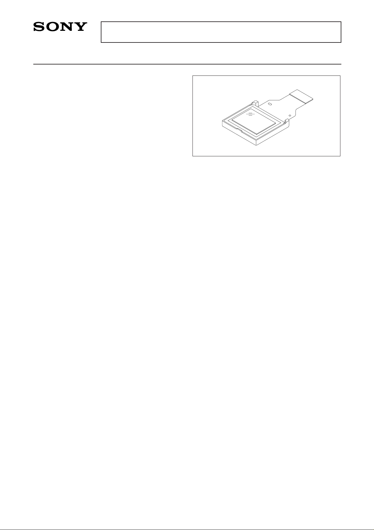
1.4cm (0.55-inch) NTSC/PAL Color LCD Panel
Description
The LCX024AK is a 1.4cm diagonal active matrix
TFT-LCD panel addressed by polycrystalline silicon
super thin film transistors with built-in peripheral
driving circuit. This panel provides full-color
representation in NTSC/PAL mode. RGB dots are
arranged in a delta pattern featuring high picture
quality of no fixed color patterns, which is inherent in
vertical stripes and mosaic pattern arrangements.
Features
• The number of active dots: 113,578 (0.55-inch; 1.397cm in diagonal)
• Horizontal resolution: 260 TV lines
• High optical transmittance: 3.4% (typ.)
• High contrast ratio with normally white mode: 270 (typ.)
• Built-in H and V drivers (built-in input level conversion circuit, TTL drive possible)
• High quality picture representation with RGB delta arranged color filters
• Full-color representation
• NTSC/PAL compatible
• Right/left inverse display function
• 4:3 and 16:9 aspect switching function
Element Structure
• Dots
Total dots : 537 (H) × 222 (V) = 119,214
Active dots: 521 (H) × 218 (V) = 113,578
• Built-in peripheral driver using polycrystalline silicon super thin film transistors.
Applications
• Viewfinders
• Super compact liquid crystal monitors etc.
LCX024AK
For the availability of this product, please contact the sales office.
– 2 –
LCX024AK
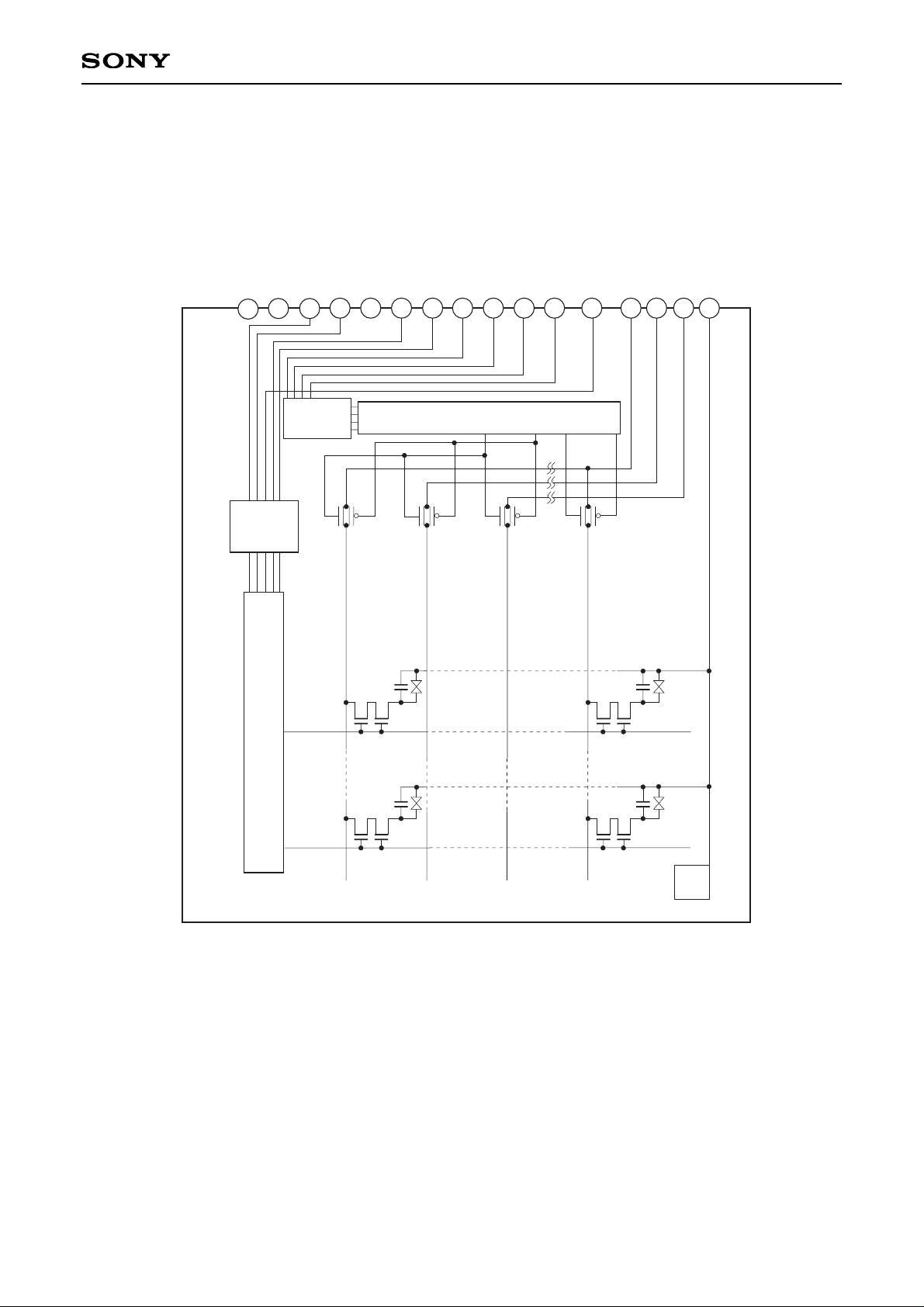
Block Diagram
1
2
3
4
5
6
7
8
9
10
11
12
13
14
15
16
H Shift Register
V Level
Conversion
Circuit
V Shift Register
CS LC
COM
Pad
V
DD
V
SS
VST
VCK
(NC)
EN
CLR
RGT
HST
HCK2
HCK1
BLK
BLUE
RED
GREEN
COM
H Level
Conversion
Circuit
– 3 –
LCX024AK
Absolute Maximum Ratings (VSS = 0V)
• H and V driver supply voltages VDD –1.0 to +17 V
• H driver input pin voltage HST, HCK1, HCK2 –1.0 to +17 V
RGT
• V driver input pin voltage VST, VCK –1.0 to +17 V
CLR, EN, BLK
• Video signal input pin voltage GREEN, RED, BLUE –1.0 to +15 V
• Operating temperature Topr –10 to +70 °C
• Storage temperature Tstg –30 to +85 °C
Operating Conditions (VSS = 0V)
Supply voltage
VDD 11.4 to 14.0 V
Input pulse voltage (Vp-p of all input pins except video signal input pins)
Vin 2.6V (more than)
Pin Description
Pin
No.
1
2
3
4
5
6
7
8
COM
GREEN
RED
BLUE
BLK
HCK1
HCK2
HST
Common voltage of panel
Video signal (G) to panel
Video signal (R) to panel
Video signal (B) to panel
Top/bottom block display pulse
Clock pulse for H shift register
drive
Clock pulse for H shift register
drive
Start pulse for H shift register
drive
9
10
11
(12)
13
14
15
16
RGT
CLR
EN
(NC)
VCK
VST
Vss
VDD
Drive direction pulse for H shift
register (H: normal, L: reverse)
Improvement pulse for
uniformity
Enable pulse for gate selection
Not connected
Clock pulse for V shift register
drive
Start pulse for V shift register
drive
GND (H, V drivers)
Power supply for H and V drivers
Symbol Description
Pin
No.
Symbol Description
– 4 –
LCX024AK
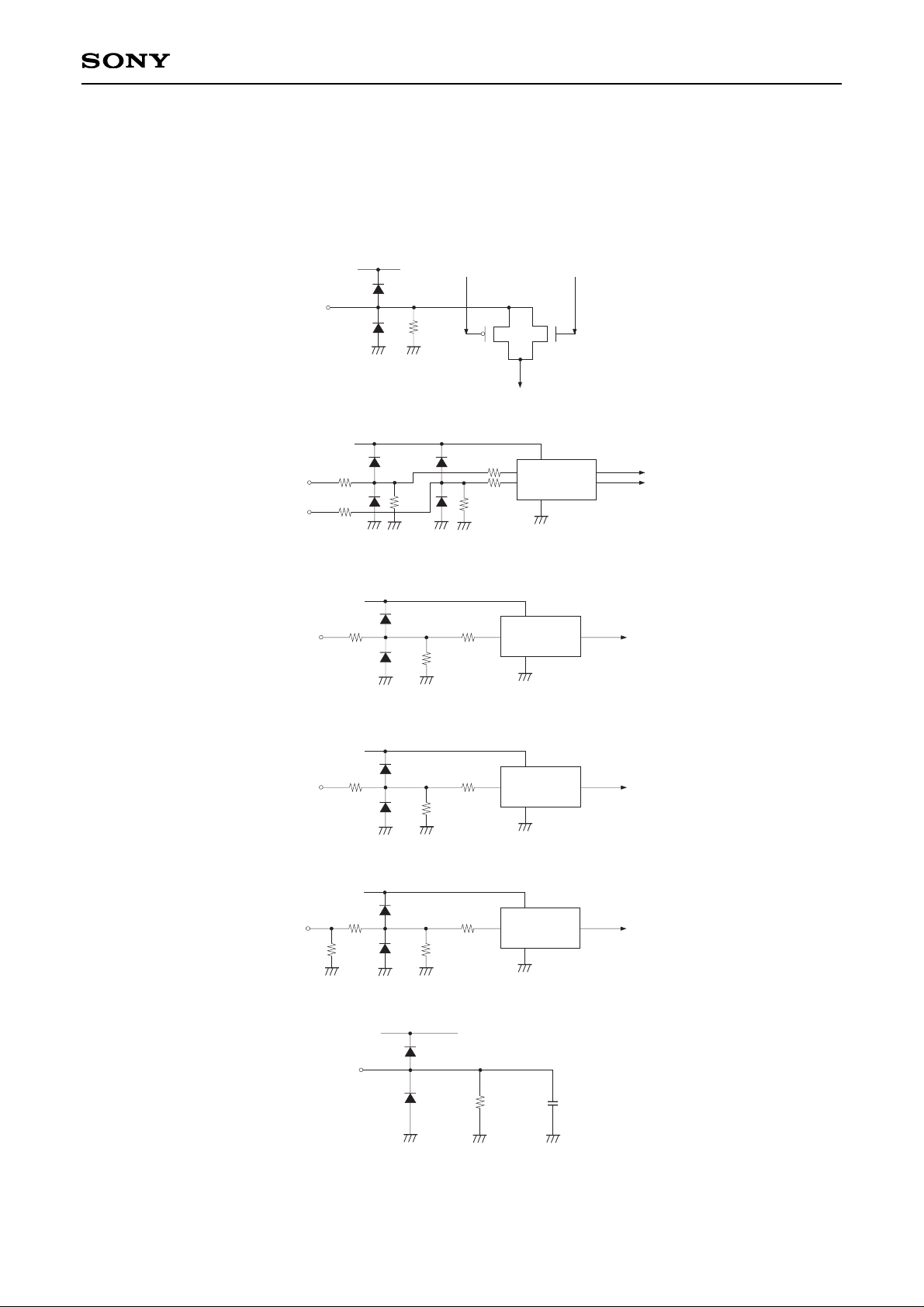
Input Equivalent Circuit
To prevent static charges, protective diodes are provided for each pin except the power supply. In addition,
protective resistors are added to all pins except video signal input. All pins are connected to Vss with a high
resistance of 1MΩ (typ.). The equivalent circuit of each input pin is shown below: (The resistor value: typ.)
(1) Video signal input
Input
V
DD
From H driver
Signal line
1MΩ
(2) HCK1, HCK2
VDD
250Ω
250Ω
250Ω
250Ω
Level conversion
circuit (2-phase
input)
HCK1
HCK2
1MΩ
1MΩ
(3) HST
Level conversion
circuit (singlephase input)
250Ω250Ω
V
DD
Input
1MΩ
(4) RGT, VST, CLR, EN, VCK
Level conversion
circuit (singlephase input)
2.5kΩ
2.5kΩ
V
DD
Input
1MΩ
(6) COM
Input
1MΩ
LC
VDD
Level conversion
circuit (singlephase input)
2.5kΩ2.5kΩ
VDD
Input
1MΩ
28kΩ
(5) BLK
– 5 –
LCX024AK
Level Conversion Circuit
The LCX024AK has a built-in level conversion circuit in the clock input unit located inside the panel. The circuit
voltage is stepped up to VDD inside the panel. This level conversion circuit meets the specifications of a 3.0V
power supply of the externally-driven IC.
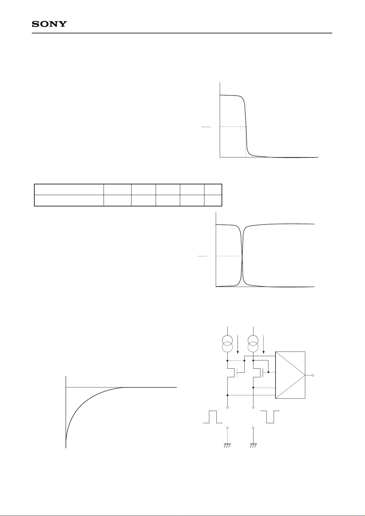
1. I/O characteristics of level conversion circuit
(For a single-phase input unit)
An example of the I/O voltage characteristics of a
level conversion circuit is shown in the figure to the
right. The input voltage value that becomes half the
output voltage (after voltage conversion) is defined
as Vth.
The Vth value varies depending on the VDD voltage.
The Vth values under standard conditions are
indicated in the table below. (HST, VST, EN, CLR,
RGT, VCK and BLK in the case of a single-phase input)
VDD = 12.0V
VDD
2
VDD
Vth
Input voltage [V]
Example of single-phase
I/O characteristics
Output voltage (inside panel)
Item
Vth voltage of circuit Vth 0.35 1.50 2.60 V
Symbol Min. Typ. Max. Unit
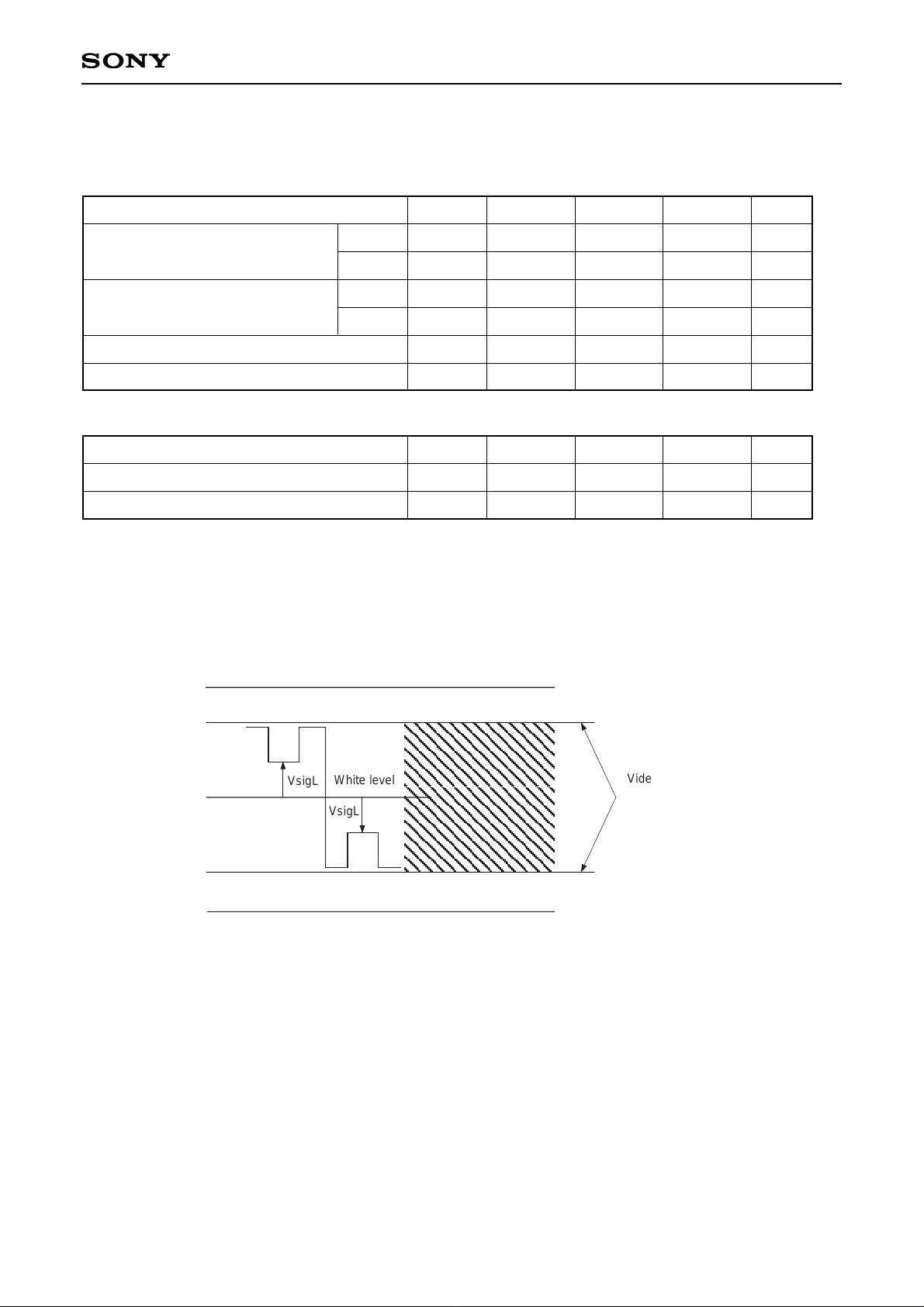
(For a differential input unit)
An example of I/O voltage characteristics of a level
conversion circuit for a differential input is shown in
the figure to the right. Although the characteristics,
including those of the Vth voltage, are basically the
same as those for a single-phased input, the twophased input phase is defined. (Refer to clock
timing conditions.)
VDD
2
VDD
Vth
Input voltage [V]
Example of differential I/O
characteristics
Output voltage (inside panel)
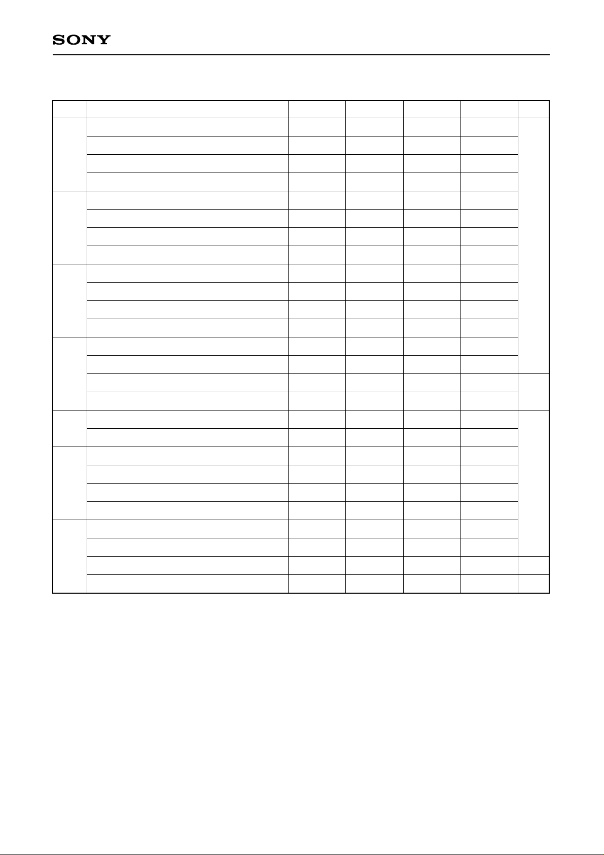
2. Current characteristics at the input pin of level conversion circuit
A slight pull-in current is generated at the input pin
of the level conversion circuit. (The equivalent
circuit is shown to the right.) The current volume
increases as the voltage at the input pin decreases,
and is maximized when the pin is grounded. (Refer
to electrical characteristics.)
VDD
output
HCK1
input
HCK2
input
Level conversion equivalent circuit
0
0
Max. value
Input pin voltage [V]
10
Pull-in current characteristics at the input pin
Input pin current
– 6 –
LCX024AK
Input Signals
1. Input signal voltage conditions (VSS = 0V, VDD = 11.4 to 14V)
Item
H driver input voltage
(HST, HCK1, HCK2, RGT)
(Low)
(High)
(Low)
(High)
VHIL
VHIH
VVIL
VVIH
VVC
VCOM
–0.35
2.6
–0.35
2.6
5.8
VVC – 0.45
0.0
5.0
0.0
5.0
6.0
VVC – 0.3
0.35
5.5
0.35
5.5
6.2
VVC – 0.15
V
V
V
V
V
V
V driver input voltage
(VST, VCK1, VCK2, CLR, EN)
Video signal center voltage
Common voltage of panel
Symbol Min. Typ. Max. Unit
Note) Video signal shall be symmetrical to VVC.
Supplement) Video signal input range is set within the range shown below for VDD and VSS.
Also, video signal white level is defined for VVC as shown below.
Item
Video signal input range
Video signal input white level
Vsig
VsigL
VSS + 1.3
0.5
VDD – 1.8 V
V
Symbol Min. Typ. Max. Unit
A
A
A
VsigL
White level
VsigL
Video signal input range
Max. VDD – 1.8 [V]
Min. VSS + 1.3 [V]
V
DD
VDD – 1.8
VVC
V
SS + 1.3
V
SS
AAA
AAA
AAA
– 7 –
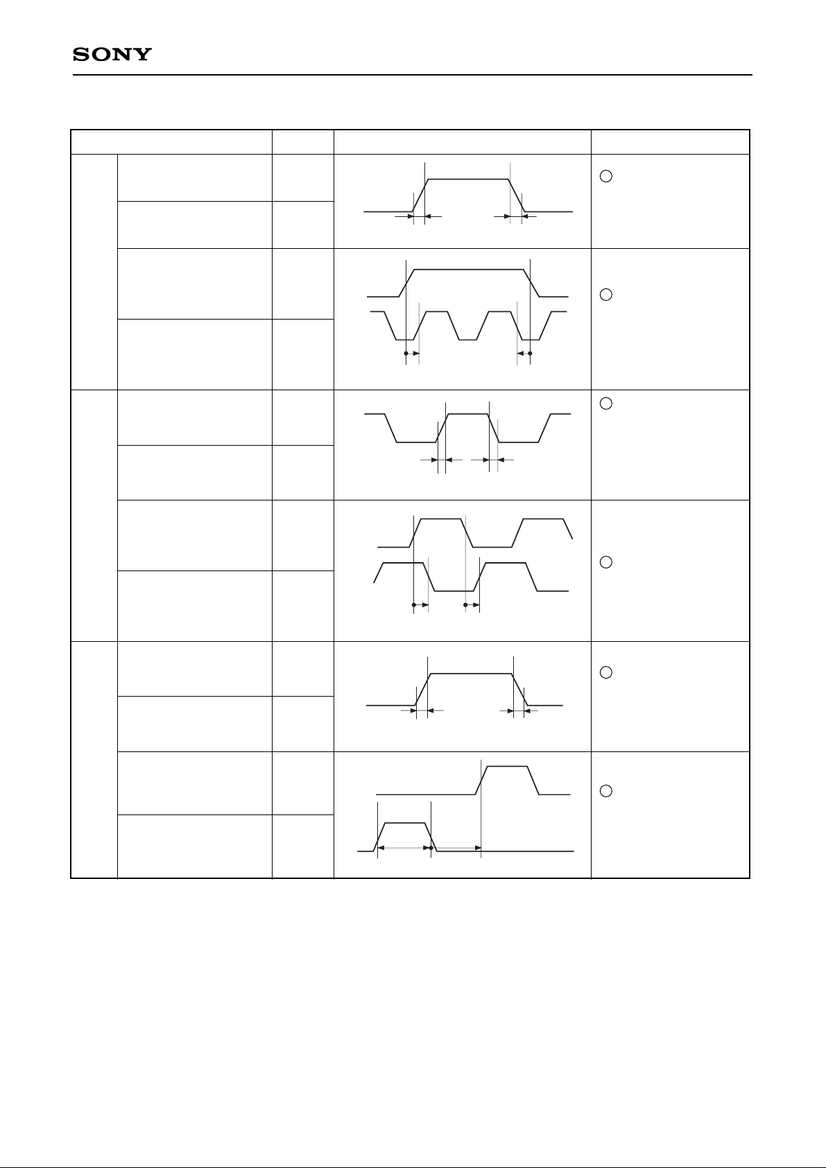
LCX024AK
Hst rise time
Hst fall time
Hst data set-up time
Hst data hold time
Hckn∗2rise time
Hckn∗2fall time
Hck1 fall to Hck2 rise time
Hck1 rise to Hck2 fall time
Clr rise time
Clr fall time
Clr pulse width
Clr fall to Hst rise time
Vst rise time
Vst fall time
Vst data set-up time
Vst data hold time
Vck rise time
Vck fall time
En rise time
En fall time
Vck fall to En fall time
Vck rise to En rise time
BLK rise time
BLK fall time
BLK pulse width
BLK fall to CLR fall time
trHst
tfHst
tdHst
thHst
trHckn
tfHckn
to1Hck
to2Hck
trClr
tfClr
twClr
toHst
trVst
tfVst
tdVst
thVst
trVck
tfVck
trEn
tfEn
tdVck2
tdVck1
trBlk
tfBlk
twBlk
toClr
–170
–455
–15
–15
3400
1100
–50
–50
–100
–100
600
135
–135
0
0
3500
1200
32
–32
0
0
1.0
700
30
30
170
–50
30
30
15
15
100
100
3600
1300
100
100
50
–20
100
100
100
100
100
100
100
100
800
ns
µs
ns
ms
ns
Item Symbol Min. Typ. Max. Unit
HST
HCK
CLR
VST
VCK
EN
BLK
∗3
∗2
Hckn means Hck1, Hck2. (fHckn = 1.84MHz, fVckn = 7.865kHz)
∗3
BLK pulse is used only for 16:9 mode. For 4:3 mode, connect to VSS.
2. Clock timing conditions (Ta = 25°C, Input voltage = 3.0V, VDD = 12.0V)
– 8 –
LCX024AK
<Horizontal Shift Register Driving Waveform>
Hst rise time
HST
HCK
CLR
Hst fall time
Hst data set-up time
Hst data hold time
Hckn∗2rise time
Hckn∗2fall time
Hck1 fall to Hck2 rise
time
Hck1 rise to Hck2 fall
time
Clr rise time
Clr fall time
Clr pulse width
Clr fall to Hst rise time
HCKn
∗2
duty cycle 50%
to1Hck = 0ns
to2Hck = 0ns
HCKn
∗2
duty cycle 50%
to1Hck = 0ns
to2Hck = 0ns
HCKn
∗2
duty cycle 50%
to1Hck = 0ns
to2Hck = 0ns
tdHst = 135ns
thHst = –135ns
tdHst = 135ns
thHst = –135ns
HCKn
∗2
duty cycle 50%
to1Hck = 0ns
to2Hck = 0ns
HCKn
∗2
duty cycle 50%
to1Hck = 0ns
to2Hck = 0ns
trHst
tfHst
tdHst
thHst
trHckn
tfHckn
to1Hck
to2Hck
trClr
tfClr
twClr
toHst
Item Symbol Waveform Conditions
10%
HST
90%
90%
10%
∗
4
HST
HCK1
trHst tfHst
50%
50%
50%
50%
∗
HCKn
tdHst thHst
90%
2
10%
90%
10%
∗
4
HCK1
HCK2
trHckn tfHckn
50%
50%
to2Hck to1Hck
50%
50%
CLR
HST
CLR
90%
10%
trClr tfClr
50%
50% 50%
twClr toHst
90%
10%

– 9 –
LCX024AK
∗4
Definitions: The right-pointing arrow ( ) means +.
The left-pointing arrow ( ) means –.
The black dot at an arrow ( ) indicates the start of measurement.
<Vertical Shift Register Driving Waveform>
Vst rise time
VST
VCK
EN
Vst fall time
Vst data set-up time
Vst data hold time
Vck rise time
Vck fall time
En rise time
En fall time
Vck rise to En rise time
Vck rise to En fall time
VCK
duty cycle 50%
VCK
duty cycle 50%
VCK
duty cycle 50%
tdVst = 32µs
thVst = –32µs
VCK
duty cycle 50%
to1Vck = 0ns
to2Vck = 0ns
VCK
duty cycle 50%
to1Vck = 0ns
to2Vck = 0ns
trVst
tfVst
tdVst
thVst
trVck
tfVck
trEn
tfEn
tdVck
tdVck
BLK
BLK rise time
BLK fall time
BLK pulse width
BLK fall to CLR fall
time
trBlk
tfBlk
twBlk
toClr
Item Symbol Waveform Conditions
VST
10%
90%
90%
10%
∗
4
VST
trVst tfVst
50%
50%
50%
50%
VCK
VCK
tdVst thVst
90%
10%
90%
10%
EN
trVck tfVck
90%
10%
10%
90%
∗
4
VCK
50%
tfEn trEn
50%
∗
4
BLK
CLR
EN
50%
50%
tdVck tdVck
90%
10%
trBlk tfBlk
twBlk
50%
90%
10%
50%
50%

– 10 –
LCX024AK
Electrical Characteristics
1. Horizontal drivers
(Ta = 25°C, VDD = 12.0V, Input voltage = 3.0V)
Item
Input pin capacitance HCKn
HST
Input pin current HCK1
HCK2
HST
RGT
Video signal input pin capacitance
CHckn
CHst
IHck1
IHck2
IHst
IRgt
Csig
HCK1 = GND
HCK2 = GND
HST = GND
RGT = GND
–500
–500
–300
–100
5
5
–250
–250
–100
–25
35
10
10
45
pF
pF
µA
µA
µA
µA
pF
Symbol Min. Typ. Max. Unit Condition
2. Vertical drivers
Item
Input pin capacitance VCK
VST
VST
EN
CLR
VCK
BLK
CVck
CVst
IVst
IEn
IClr
IVck
IBlk
–100
5
5
–25
10
10
pF
pF
µA
Symbol Min. Typ. Max. Unit Condition
3. Total power consumption of the panel
Item
Total power consumption of
the panel (NTSC)
PWR 30 50 mW
Symbol Min. Typ. Max. Unit
4. VCOM input resistance
Item
VCOM – Vss input resistance Rcom 0.5 1 MΩ
Symbol Min. Typ. Max. Unit
VST, EN, CLR, VCK,
BLK = GND

– 11 –
LCX024AK
Electro-optical Characteristics (Ta = 25°C, NTSC mode)
Item
Contrast
ratio
VDD = 12.0V
Vsig = 6.0 ± 4.0V
VDD = 13.5V
Vsig = 6.0 ± 4.5V
60°C
25°C
60°C
25°C
X
Y
X
Y
X
Y
25°C
60°C
25°C
60°C
25°C
60°C
R vs. G
B vs. G
0°C
25°C
0°C
25°C
60°C
60 min.
CR4.060
CR4.025
CR4.560
CR4.525
T
Rx
Ry
Gx
Gy
Bx
By
V90-25
V90-60
V50-25
V50-60
V10-25
V10-60
V50RG
V50BG
ton0
ton25
toff0
toff25
F
YT60
70
70
80
80
2.6
0.560
0.300
0.275
0.541
0.120
0.040
1.1
1.0
1.5
1.4
2.2
2.1
—
—
—
—
—
—
—
—
200
200
270
270
3.4
0.630
0.345
0.310
0.595
0.148
0.088
1.6
1.5
2.0
1.8
2.5
2.4
–0.10
0.10
30
8
65
20
—
—
—
—
—
—
—
0.670
0.390
0.347
0.650
0.187
0.122
2.2
2.1
2.5
2.4
3.2
3.1
–0.25
0.45
100
40
150
60
–40
20
1
2
3
4
5
6
7
8
—
%
CIE
standards
V
V
ms
dB
s
Optical transmittance
Chromaticity
R
G
B
V90
V50
V10
ON time
OFF time
V-T
characteristics
Half tone color reproduction
range
Response time
Flicker
Image retention time
Symbol
Measurement
method
Min Typ. Max.
Unit

– 12 –
LCX024AK
<Electro-optical Characteristics Measurement>
Basic measurement conditions
(1) Driving voltage
VDD = 13.5V
VVC = 6.0V, VCOM = 5.7V
(2) Measurement temperature
25°C unless otherwise specified.
(3) Measurement point
One point in the center of screen unless otherwise specified.
(4) Measurement systems
Two types of measurement system are used as shown below.
(5) RGB input signal voltage (Vsig)
Vsig = 6.0 ± VAC [V] (VAC: signal amplitude)
∗
Measurement system I
LCD panel
Luminance
Meter
Measurement
Equipment
Back light: color temperature 6500K, +0.004uV (25°C)
∗
Back light spectrum (reference) is listed on another page.
Optical fiber
LCD panel
Light receptor lens
Drive Circuit
Light Source
Back Light
3.5mm
∗
Measurement system II
Measurement
Equipment
Light Detector
1. Contrast Ratio
Contrast Ratio (CR4.0) is given by the following formula (1).
CR4.0 = ...(1)
L4.0 (White): Surface luminance of the TFT-LCD panel at VDD = 12.0V, VVC = 6.0V, VCOM = 5.7V and the
RGB signal amplitude VAC = 0.5V.
L4.0 (Black): Surface luminance of the panel at VAC = 4.0V.
Contrast Ratio (CR4.5) is given by the following formula (2).
CR4.5 = ...(2)
L4.5 (White): Surface luminance of the TFT-LCD panel at the RGB signal amplitude VAC = 0.5V.
L4.5 (Black): Surface luminance of the panel at VAC = 4.5V.
The above luminosities are measured by System I.
L4.0 (White)
L4.0 (Black)
L4.5 (White)
L4.5 (Black)

– 13 –
LCX024AK
2. Optical Transmittance
Optical Transmittance (T) is given by the following formula (2).
T = × 100 [%] ...(2)
L (White) is the same expression as defined in the "Contrast Ratio" section.
3. Chromaticity
Chromaticity of the panels are measured by System I. Raster modes of each color are defined by the
representations at the input signal amplitude conditions shown in the table below. System I uses
Chromaticity of x and y on the CIE standards here.
Signal amplitudes (VAC) supplied to each input
R input G input B input
Raster
R
G
B
0.5
4.5
4.5
4.5
0.5
4.5
4.5
4.5
0.5
(Unit : V)
4. V-T Characteristics
V-T characteristics, the relationship between signal
amplitude and the transmittance of the panels, are
measured by System II. V90, V50 and V10 correspond to
the each voltage which defines 90%, 50% and 10% of
transmittance respectively. (Transmittance at VAC =
0.5V is 100%.)
5. Half Tone Color Reproduction Range
Half tone color reproduction range of the LCD panels is
characterized by the differences between the V-T
characteristics of R, G and B. The differences of these
V-T characteristics are measured by System II. System
II defines signal voltages of each R, G, B raster modes
which correspond to 50% of transmittance, V50R, V50G
and V50B respectively. V50RG and V50BG, the voltage
differences between V50R and V50G, V50B and V50G, are
simply given by the following formulas (3) and (4)
respectively.
V50RG = V50R – V50G ...(3)
V50BG = V50B – V50G ...(4)
90
50
10
V
90 V50 V10
VAC – Signal amplitude [V]
Transmittance [%]
100
50
0
V
50R V50B
V50G
VAC – Signal amplitude [V]
Transmittance [%]
V50RG
V50BG
G raster
B raster
R raster
L (White)
Luminance of Back Light

– 14 –
LCX024AK
6. Response Time
Response time ton and toff are defined by
the formulas (5) and (6) respectively.
ton = t1 – tON ...(5)
toff = t2 – tOFF ...(6)
t1: time which gives 10% transmittance of
the panel.
t2: time which gives 90% transmittance of
the panel.
The relationships between t1, t2, tON and
tOFF are shown in the right figure.
7. Flicker
Flicker (F) is given by the formula (7). DC and AC (NTSC: 30Hz, rms, PAL: 25Hz, rms) components of the
panel output signal for gray raster∗mode are measured by a DC voltmeter and a spectrum analyzer in
System II.
F (dB) = 20log
{ }
...(7)
8. Image Retention Time
Apply the monoscope signal to the LCD panel for 60 minutes and then change this signal to the gray scale
of Vsig = 6.0 ± VAC (VAC: 3 to 4V), judging by sight at VAC that hold the maximum image retention, measure
the time till the residual image becomes indistinct.
∗
Monoscope signal conditions:
Vsig = 6.0 ± 4.5 or 6 ±2.0 (V)
(shown in the right figure)
VCOM = 5.7V
Input signal voltage (waveform applied to the measured pixels)
4.5V
0.5V
6.0V
0V
Optical transmittance output waveform
100%
90%
10%
0%
tON t1
ton
tOFF t2
toff
∗
R, G, B input signal condition for gray raster mode
is given by Vsig = 6.0 ± V50 (V)
where: V50 is the signal amplitude which gives 50%
of transmittance in V-T characteristics.
Black level
White level
Vsig waveform
6.0V
0V
4.5V
2.0V
4.5V
2.0V
AC component
DC component

– 15 –
LCX024AK
Example of Back Light Spectrum (Reference)
0.4
0.3
0.2
0.1
0
400 500 600 700
Wavelength 380 – 780 [nm]

– 16 –
LCX024AK
Description of Operation
1. Color Coding
Color filters are coded in a delta arrangement.
The shaded area is used for the dark border around the display.
B R G B R G B R G B R G B R G B R
GRBGRBGRBGRBGRBGR
B R G B R G B R G B R G B R G B R
GRBGRBGRBGRBGRBGR
B R G B R G B R G B R G B R G B R
GRBGRBGRBGRBGRBGR
B R G B R G B R G B R G B R G B R
GRBGRBGRBGRBGRBGR
B R G B R G B R G B R G B R G B R
RBGRBGRBGRBGRBGR
G
Gate SW Gate SW Gate SW Gate SW
537
3 521 13
2
2
218
222
Gate SW Gate SW
Green is not
connected
for only final
stage.
Photo-shielding
G
B
G
B
G
B
G
B
G
B
Active area

– 17 –
LCX024AK
2. LCD Panel Operations
• A vertical driver, which consists of vertical shift registers, enable-gates and buffers, applies a selected pulse
to every 218 gate lines sequentially in every horizontal scanning period. A vertical shift register scans the
gate lines from the top to bottom of the panel.
• The selected pulse is delivered when the enable pin turns to High level. PAL mode images are displayed by
controlling the enable and VCK pin. The enable pin should be High when not in use.
• A horizontal driver, which consists of horizontal shift registers, gates and CMOS sample-and-hold circuits
applies selected pulses to every 521 signal electrodes sequentially in a single horizontal scanning period.
• Scanning direction of horizontal shift register can be switched with RGT pin. Scanning direction is left to right
for RGT pin at High level; and right to left for RGT pin at Low level. (These scanning directions are from a
front view.) Normally, set to High level.
• Vertical and horizontal drivers address one pixel and then turn on Thin Film Transistors (TFTs; two TFTs) to
apply a video signal to the dot. The same procedures lead to the entire 218 × 521 dots to display a picture in
a single vertical scanning period.
• Pixel dots are arranged in a delta pattern, where sets of RGB pixels are positioned with 1.5-dot shifted
against adjacent horizontal line. 1.5-dot shift of a horizontal driver output pulse against horizontal
synchronized signal is required to apply a video signal to each dot properly. 1H reversed displaying mode is
required to apply video signal to the panel.
• The CLR pin is provided to eliminate the shading effect caused by the coupling of selected pulses. While
maintaining the CLR at High level, the VDD potential of gate output inverter drops to approximately 8.5V. This
pin shall be grounded when not in use.
• The video signal shall be input with polarity-inverted system in every horizontal cycle.
• Timing diagrams of the vertical and the horizontal right-direction scanning (RGT = High level) display cycle
are shown below:
Vertical display cycle 218H (13.84ms)
1 2 218217
(1) Vertical display cycle
VD
VST
VCK
Horizontal display cycle (47.3µs)
1 2 3 4 5
175
174
(2) Horizontal display cycle (right scan)
HD
HST
HCK1
HCK2
∗
HST is sampled at first for HCK1.
The horizontal display cycle consists of 521/3 = 174 clock pulses because of RGB simultaneous sampling.
∗
Refer to Description of Operation "3. RGB Simultaneous Sampling."
∗
VST is sampled at first for VCK.

– 18 –
LCX024AK
3. RGB Simultaneous Sampling
Horizontal driver samples R, G and B signal simultaneously, which requires the phase matching between R,
G and B signals to prevent horizontal resolution from deteriorating. Thus phase matching between each
signal is required using an external signal delaying circuit before applying video signal to the LCD panel.
Two methods are applied for the delaying procedure: Sample and hold and Delay circuit. These two block
diagrams are as follows.
The LCX024AK has the right/left inverse function. The following phase relationship diagram indicates the
phase setting for the right scan (RGT = High level). For the left scan (RGT = Low level), the phase setting
shall be inverted between B and G signals.
(1) Sample and hold (right scan)
<Phase relationship of delaying sample-and-hold pulses> (right scan)
S/H S/H AC Amp
S/H AC Amp
S/H AC Amp
S/H
(2) Delay circuit (right scan)
Delay Delay AC Amp
Delay AC Amp
AC Amp
4
3
B
R
G
BLUE
RED
GREEN
CKB
CKR
CKG
CKG
CKG
HCKn
CKB
CKR
CKG
BLUE
RED
GREEN
B
R
G
LCX024AK
LCX024AK
2
4
3
2

– 19 –
LCX024AK
Example of Color Filter Spectrum (Reference)
400 500 600 700
Wavelength [nm]
Transmittance [%]
0
20
40
60
80
100
B
G
R
Color Filter Spectrum

– 20 –
LCX024AK
Color Display System Block Diagram (1)
An example of dual-chip display system is shown below.
Y/color difference
Y/C
LCD panel
NTSC/PAL
LCX024AK
Decoder/Driver
CXA1785AR
TG
CXD2458AR
RED
GREEN
BLUE
HCK1
HST
VST
HCK2
BLK
EN
VCK
CLR
RGT
(Refer to CXD2458AR data sheet.)
+3V
FRPSYNC
Composite video
+12V +5V +12.0 or 13.5V
VCOM

– 21 –
LCX024AK
Color Display System Block Diagram (2)
An example of single-chip display system is shown below.
Y/color difference
Y/C
LCD panel
NTSC/PAL
LCX024AK
CXA2503AR
RED
GREEN
BLUE
HCK1
HST
VST
HCK2
VCK
EN
CLR
RGT
(Refer to CXA2503AR data sheet.)
Composite video
+12V +5V +12.0 or +13.5V
VCOM
When the CXA2503AR is used, connect BLK (Pin 5) of the LCD panel to VSS or leave that pin open. The
LCX024AK specification conforms to the LCX005BK specification.

– 22 –
LCX024AK
Color Display System Block Diagram (3)
An example of dual-chip display system is shown below.
Y/color difference
Y/C
LCD panel
NTSC/PAL
LCX024AK
Decoder/Driver
CXA1785AR
TG
CXD2411AR
RED
GREEN
BLUE
HCK1
HST
VST
HCK2
EN
VCK
CLR
RGT
(Refer to CXD2411AR data sheet.)
+5V
FRPSYNC
Composite video
+12V +5V +12.0 or +13.5V
VCOM
When the CXA1785AR and the CXD2411AR are used, connect BLK (Pin 5) of the LCD panel to VSS or leave
that pin open. The LCX024AK specification conforms to the LCX005BK specification.

– 23 –
LCX024AK
Notes on Handling
(1) Static charge prevention
Be sure to take following protective measures. TFT-LCD panels are easily damaged by static charge.
a) Use non-chargeable gloves, or simply use bare hands.
b) Use an earth-band when handling.
c) Do not touch any electrodes of a panel.
d) Wear non-chargeable clothes and conductive shoes.
e) Install conductive mat on the working floor and working table.
f) Keep panels away from any charged materials.
g) Use ionized air to discharge the panels.
(2) Protection from dust and dirt
a) Operate in clean environment.
b) When delivered, a surface of a panel (Polarizer) is covered by a protective sheet. Peel off the
protective sheet carefully not to damage the panel.
c) Do not touch the surface of a panel. The surface is easily scratched. When cleaning, use a clean-room
wiper with isopropyl alcohol. Be careful not to leave stain on the surface.
d) Use ionized air to blow off dust at a panel.
(3) Other handling precautions
a) Do not twist or bend the flexible PC board especially at the connecting region because the board is
easily deformed.
b) Do not drop a panel.
c) Do not twist or bend a panel or a panel frame.
d) Keep a panel away from heat source.
e) Do not dampen a panel with water or other solvents.
f) Avoid to store or to use a panel in a high temperature or in a high humidity, which may result in panel
damages.

– 24 –
LCX024AK
Package Outline Unit: mm
PIN 1
PIN 16
0.5 ± 0.1
P 0.5 ± 0.02 × 15 = 7.5 ± 0.03
0.5 ± 0.15
3.0 ± 0.3
4.0 ± 0.5
18.0 ± 0.15
9.0 ± 0.25
(11.2)
2.7 ± 0.15
(8.3)
7.7 ± 0.25
17.8 ± 0.15
25.5 ± 0.8
34.8 ± 0.8
1.2 ± 0.3
Thickness of the connector 0.3 ± 0.05
14.0 ± 0.3
8.5 ± 0.05
4-R1.0
0.35
+ 0.04
– 0.03
S-C K1
Description
Molding material
Outside frame
Reinforcing board
Reinforcing material
Polarizing film
F P C
No
1
2
3
4
5
6
weight 1.3g
electrode (enlarged)
Active Area
Active Area
Incident
light
1
2
3
4
5
6
6
 Loading...