

Page 1
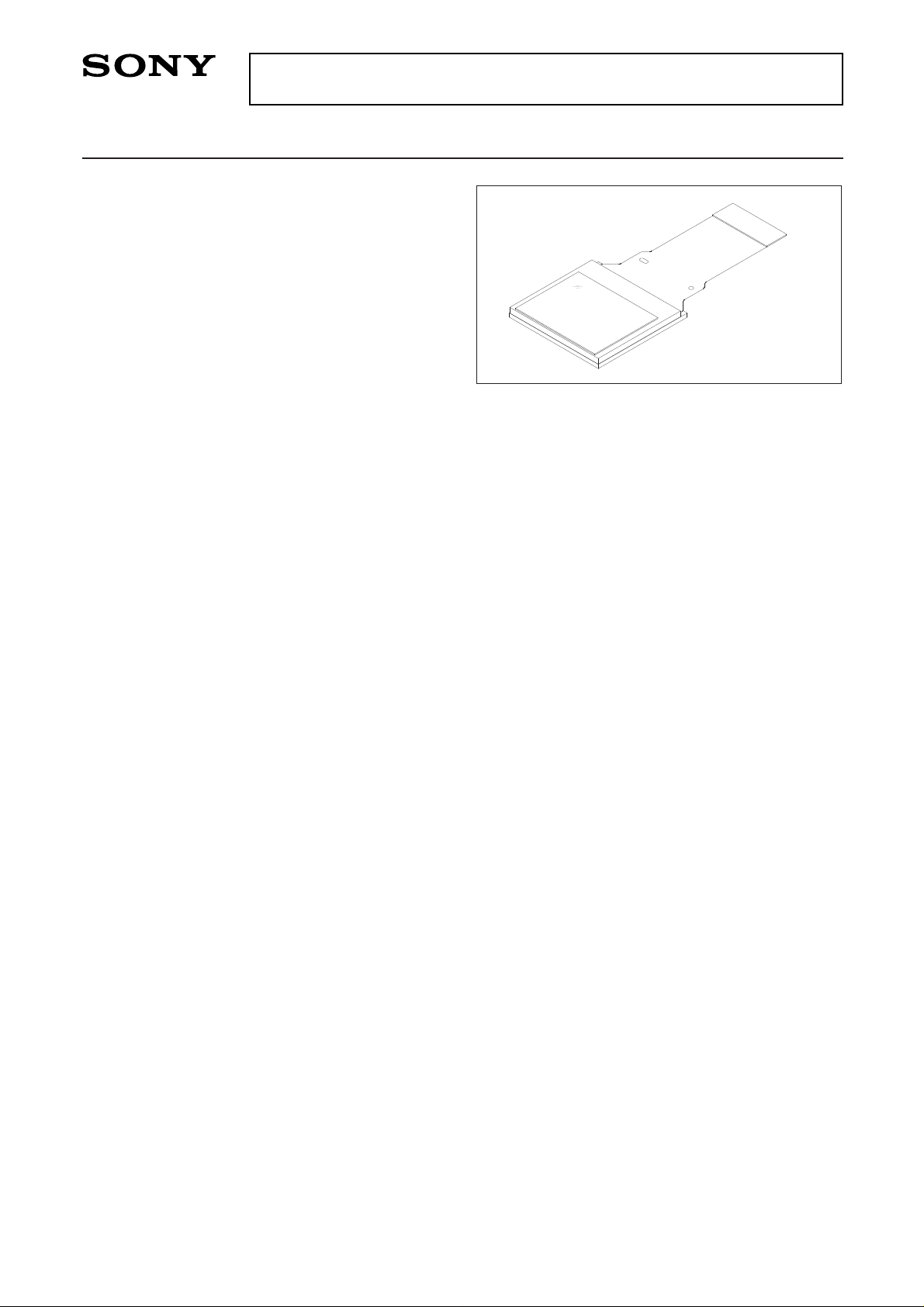
1.8cm (0.7-inch) Color LCD Panel
Description
The LCX020BK is a 1.8cm diagonal active matrix
TFT-LCD panel addressed by polycrystalline silicon
super thin film transistors with built-in peripheral driving
circuit. This panel provides full-color representation.
RGB dots are arranged in a striped pattern optimum
for data applications and capable of displaying fine
text and vertical lines.
The adoption of an advanced on-chip black matrix
realizes a high luminance screen, and high picture
quality is possible with built-in cross talk free and
ghost free circuits.
This panel has a polysilicon TFT high-speed
scanner and built-in function to display images
up/down and/or right/left inverse. In addition, the
built-in 5V interface circuit leads to lower voltage of
timing and control signals.
The panel contains a display area varying circuit
which supports Macintosh16∗1/SVGA/VGA/PC98
∗2
data signals by changing the display area according
to the type of input signal. In addition, double-speed
processed NTSC/PAL/WIDE can also be supported.
∗1
"Macintosh" is a trademark of Apple Company Inc.
∗2
"PC98" is a trademark of NEC.
Features
• Number of active dots: 1,557,000, 1.8cm (0.7-inch) in diagonal
• Supports Macintosh16 (832 × 624), SVGA (800 × 600), VGA (640 × 480) and PC98 (640 × 400) display
• Supports NTSC (640 × 480), PAL (762 × 572) and WIDE (832 × 480) display by processing the video signal
at double speed
• High optical transmittance: 1% (typ.)
• Built-in cross talk free circuit
• High contrast ratio with normally white mode: 70 (typ.)
• Built-in H and V drivers (built-in input level conversion circuit, 5V driving possible)
• Up/down and/or right/left inverse display function
Element Structure
• Dots: 2496 (H) × 624 (V) = 1,557,504
• Built-in peripheral driving circuit using polycrystalline silicon super thin film transistors
Applications
• Liquid crystal EVFs for personal PCs/DVDs
• Small monitors, etc.
– 1 –
E99210-PS
Sony reserves the right to change products and specifications without prior notice. This information does not convey any license by
any implication or otherwise under any patents or other right. Application circuits shown, if any, are typical examples illustrating the
operation of the devices. Sony cannot assume responsibility for any problems arising out of the use of these circuits.
LCX020BK
Page 2
– 2 –
LCX020BK
H Shift Register (Bidirectional Scanning)
Up/Down and/or Right/Left
Inversion Control Circuit
V Shift Register (Bidirectional Scanning)
COM
Pad
COM
SIGR6
SIGR5
SIGR4
SIGR3
SIGR2
SIGR1
V
SS
VV
DD
HV
DD
MODE1
ENB
DWN
PCG
VCK
VST
RGT
BLK
HCK2
HCK1
HST
PSIGB
Black Frame Control Circuit
Black Frame Control Circuit
MODE2
MODE3
Input Signal
Level Shifter
Circuit
Precharge
Control Circuit
1
5
6
7
8
9
10
11
12
13
14
15
16
17
18
19
20
21
22
23
31
4
2
3
24
25
26
27
28
29
30
32
33
34
35
36
37
38
SIGG6
SIGG5
SIGG4
SIGG3
SIGG2
SIGG1
SIGB6
SIGB5
SIGB4
SIGB3
SIGB2
SIGB1
PSIGR
PSIGG
V Shift Register (Bidirectional Scanning)
Black Frame Control Circuit
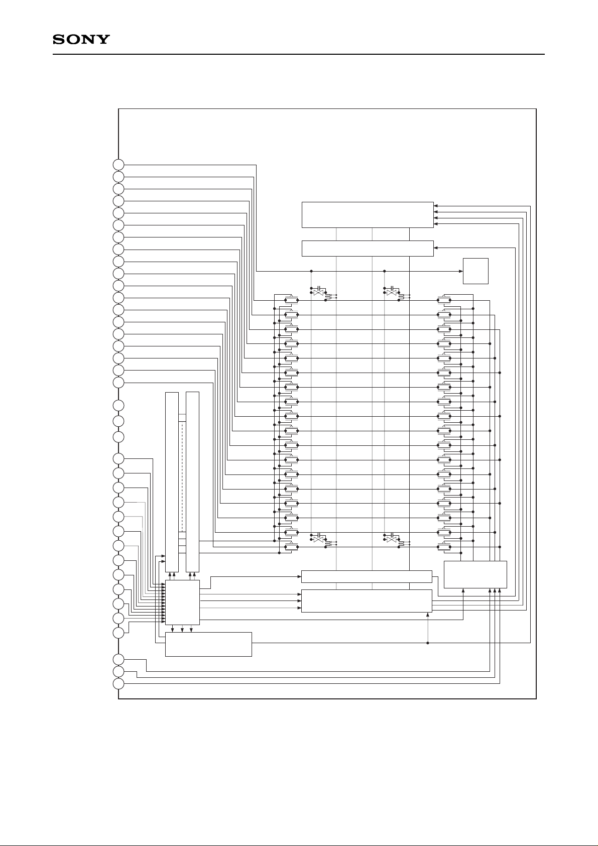
Block Diagram
The Block Diagram of the panel is shown below.
Page 3
– 3 –
LCX020BK
Absolute Maximum Ratings (Vss = 0V)
• H driver supply voltage HVDD –1.0 to +20 V
• V driver supply voltage VVDD –1.0 to +20 V
• Common pad voltage COM –1.0 to +17 V
• H shift register input pin voltage HST, HCK1, HCK2, –1.0 to +17 V
RGT
• V shift register input pin voltage VST, VCK, PCG, –1.0 to +17 V
BLK, ENB, DWN
MODE1, MODE2, MODE3
• Video signal input pin voltage SIGR1 to SIGR6, –1.0 to +15 V
SIGG1 to SIGG6,
SIGB1 to SIGB6,
PSIGR, PSIGG, PSIGB
• Operating temperature Topr –10 to +70 °C
• Storage temperature Tstg –30 to +85 °C
Operating Conditions (Vss = 0V)
• Supply voltage
HVDD 15.5 ± 0.3V
VVDD 15.5 ± 0.3V
• Input pulse voltage (Vp-p of all input pins except video signal and uniformity improvement signal input pins)
Vin 5.0 ± 0.5V
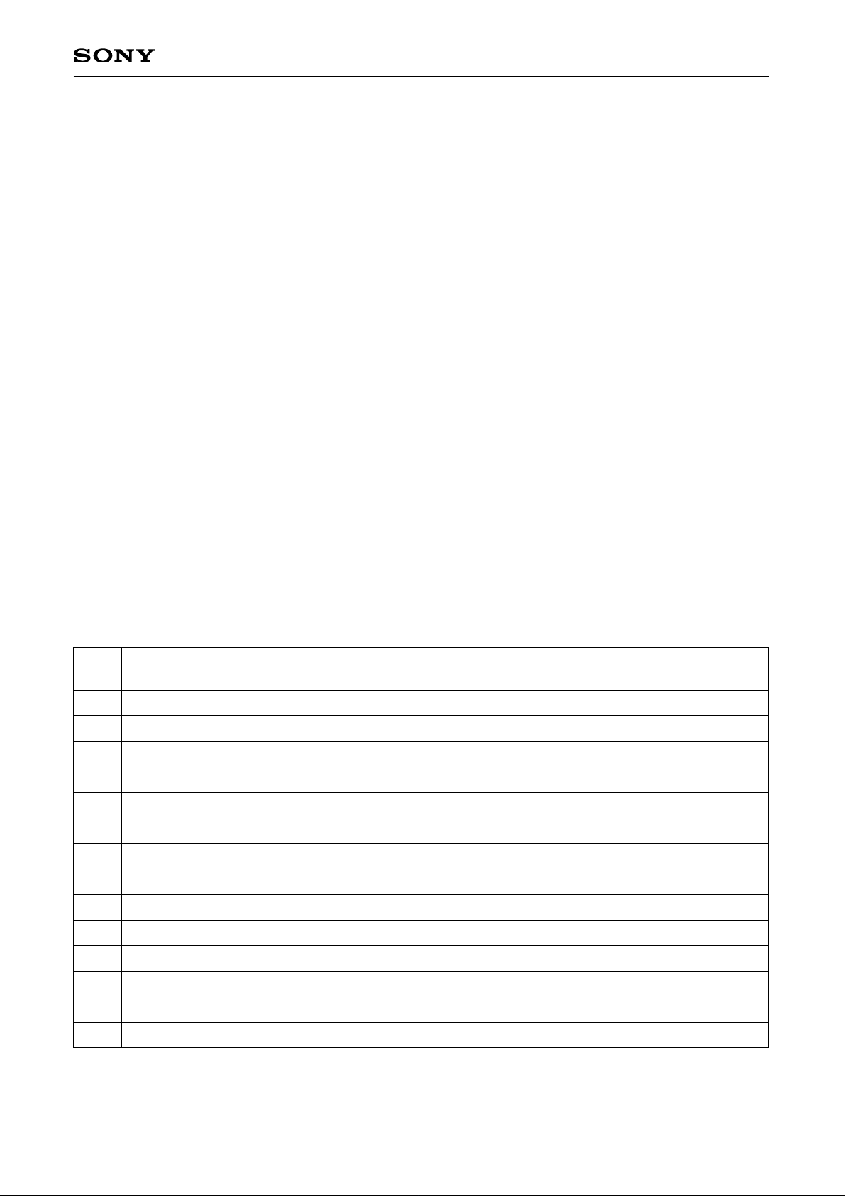
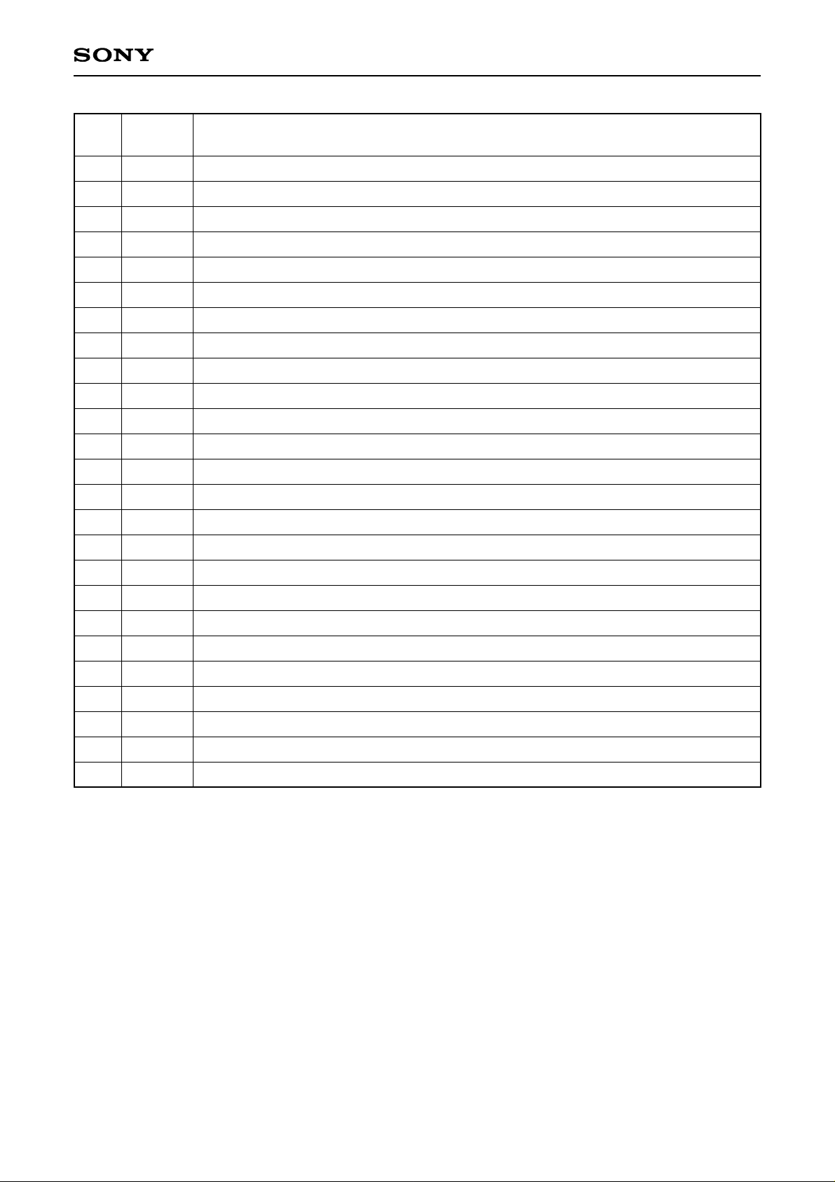
Pin Description
Pin
No.
1
2
3
4
5
6
7
8
9
10
11
12
13
14
COM
PSIGR
PSIGG
PSIGB
SIGR1
SIGR2
SIGR3
SIGR4
SIGR5
SIGR6
SIGG1
SIGG2
SIGG3
SIGG4
Common voltage of panel
Uniformity improvement signal input (R)
Uniformity improvement signal input (G)
Uniformity improvement signal input (B)
Video signal input to panel (R-1)
Video signal input to panel (R-2)
Video signal input to panel (R-3)
Video signal input to panel (R-4)
Video signal input to panel (R-5)
Video signal input to panel (R-6)
Video signal input to panel (G-1)
Video signal input to panel (G-2)
Video signal input to panel (G-3)
Video signal input to panel (G-4)
Symbol Description
Page 4
– 4 –
LCX020BK
15
16
17
18
19
20
21
22
23
24
25
26
27
28
29
30
31
32
33
34
35
36
37
38
39
SIGG5
SIGG6
SIGB1
SIGB2
SIGB3
SIGB4
SIGB5
SIGB6
HVDD
RGT
MODE3
MODE2
MODE1
HST
HCK1
HCK2
VSS
BLK
ENB
VCK
VST
DWN
PCG
VVDD
SOUT
Video signal input to panel (G-5)
Video signal input to panel (G-6)
Video signal input to panel (B-1)
Video signal input to panel (B-2)
Video signal input to panel (B-3)
Video signal input to panel (B-4)
Video signal input to panel (B-5)
Video signal input to panel (B-6)
Power supply input for H driver
Drive direction input for H shift register (H: normal, L: reverse)
Display area switching 3 input
Display area switching 2 input
Display area switching 1 input
Start pulse input for H shift register drive
Clock pulse input for H shift register drive
Clock pulse input for H shift register drive
GND (H, V drivers)
Black frame display pulse input
Gate selection pulse enable input
Clock pulse input for V shift register drive
Start pulse input for V shift register drive
Drive direction input for V shift register (H: normal, L: reverse)
Uniformity improvement pulse input
Power supply input for V driver
H and V shift register drive checking (Test pin; no connection.)
Pin
No.
Symbol Description
Page 5
– 5 –
LCX020BK
Input Equivalent Circuits
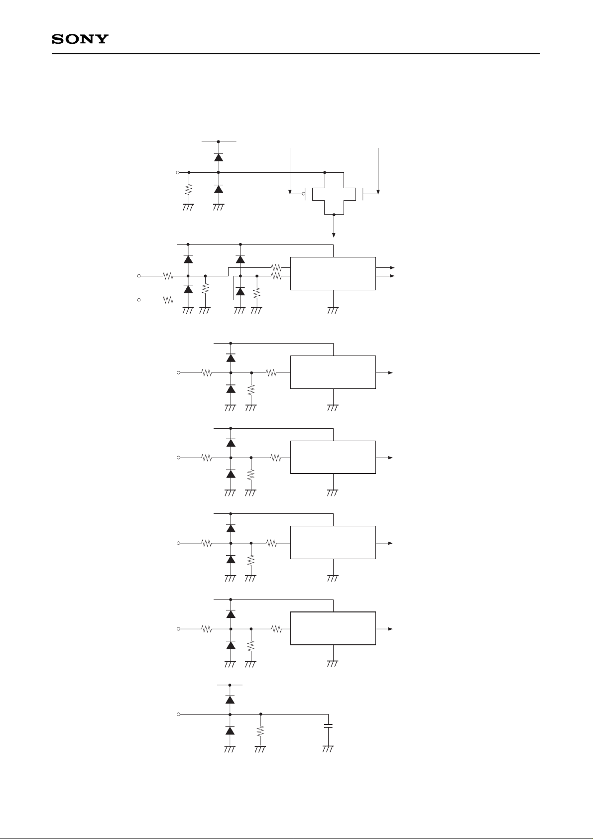
To prevent static charges, protective diodes are provided for each pin except the power supplies. In addition,
protective resistors are added to all pins except video signal inputs. All pins are connected to Vss with a high
resistance of 1MΩ (typ.). The equivalent circuit of each input pin is shown below: (Resistor value: typ.)
Input
LC
Level conversion circuit
(single-phase input)
2.5kΩ2.5kΩ
VVDD
Input
Level conversion circuit
(single-phase input)
250Ω250Ω
HV
DD
Input
Level conversion circuit
(single-phase input)
2.5kΩ2.5kΩ
HV
DD
Input
Input
HV
DD
Signal line
(1) SIGR1 to SIGR6, SIGG1 to SIGG6, SIGB1 to SIGB6, PSIGR, PSIGG, PSIGB
(2) HCK1, HCK2
(3) RGT, MODE1, MODE2, MODE3
(4) HST
(5) PCG, VCK
(6) VST, BLK, ENB, DWN
(7) COM
1MΩ
1MΩ
Level conversion circuit
(single-phase input)
250Ω250Ω
VV
DD
Input
1MW
1MΩ
1MΩ
VVDD
Input
HVDD
250Ω
250Ω
250Ω
250Ω
Level conversion circuit
(2-phase input)
1MΩ
1MΩ
1MΩ
Page 6
– 6 –
LCX020BK
Input Signals
1. Input signal voltage conditions (Vss = 0V)
Item
H shift register input voltage
HST, HCK1, HCK2, RGT
(Low)
(High)
(Low)
(High)
VHIL
VHIH
VVIL
VVIH
VVC
Vsig
Vcom
Vpsig1
Vpsig2
–0.5
4.5
–0.5
4.5
6.9
VVC – 4.5
VVC – 0.5
VVC ± 2.0
VVC ± 4.0
0.0
5.0
0.0
5.0
7.0
7.0
VVC – 0.4
VVC ± 3.0
VVC ± 4.5
0.4
5.5
0.4
5.5
7.1
VVC + 4.5
VVC – 0.3
VVC ± 4.0
VVC ± 4.6
V
V
V
V
V
V
V
V
V
V shift register input voltage
MODE1, MODE2, MODE3,
BLK, VST, VCK, PCG,
ENB, DWN
Video signal center voltage
Video signal input range
∗1
Common pad voltage of panel
∗2
Uniformity improvement signal input
voltage (PSIGR, PSIGG, PSIGB)
∗3
Symbol Min. Typ. Max. Unit
∗1
Video input signal shall be symmetrical to VVC.
∗2
The optimum typical value of the common pad voltage may lower its suitable voltage according to the set
construction to use. In this case, use the voltage of which has maximum contrast as typical value. When the
typical value is lowered, the maximum and minimum values may lower.
∗3
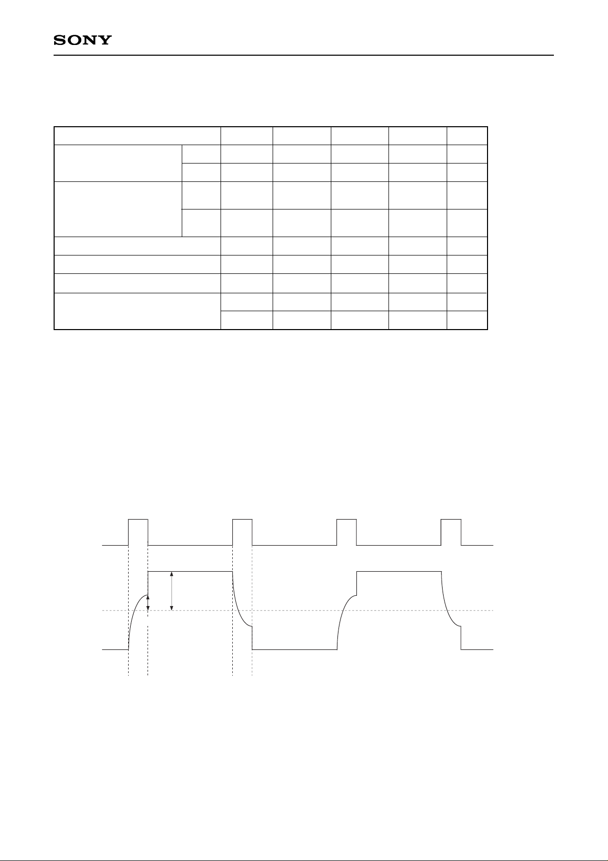
Input a uniformity improvement signals PSIGR, PSIGG and PSIGB in the same polarity with video signals
SIGR1 to 6, SIGG1 to 6 and SIGB1 to 6 and which is symmetrical to VVC. PSIGR, PSIGG and PSIGB have
two steps as shown by the waveform in the figure below, and in the table above, the upper value indicates
the signal level of the first step, and the lower value, the signal level of the second step.
Here, the rising and falling of PSIGR, PSIGG and PSIGB are synchronized with the rising of PCG pulse,
and the rise and fall times trPSIGR, trPSIGG, trPSIGB, tfPSIGR, tfPSIGG and tfPSIGB are suppressed
within 800ns.
Input waveform of uniformity improvement signal PSIG
LCX020BK level conversion circuit
The LCX020BK has a built-in level conversion circuit in the clock input unit on the panel. The input signal level
increases to HVDD or VVDD. The Vcc of external ICs are applicable to 5 ± 0.5V.
trPSIGR,
trPSIGG,
trPSIGB
10%
90%
VVC
PRG
PSIGR,
PSIGG,
PSIGB
Vpsig2
Vpsig1
tfPSIGR,
tfPSIGG,
tfPSIGB
Page 7
– 7 –
LCX020BK
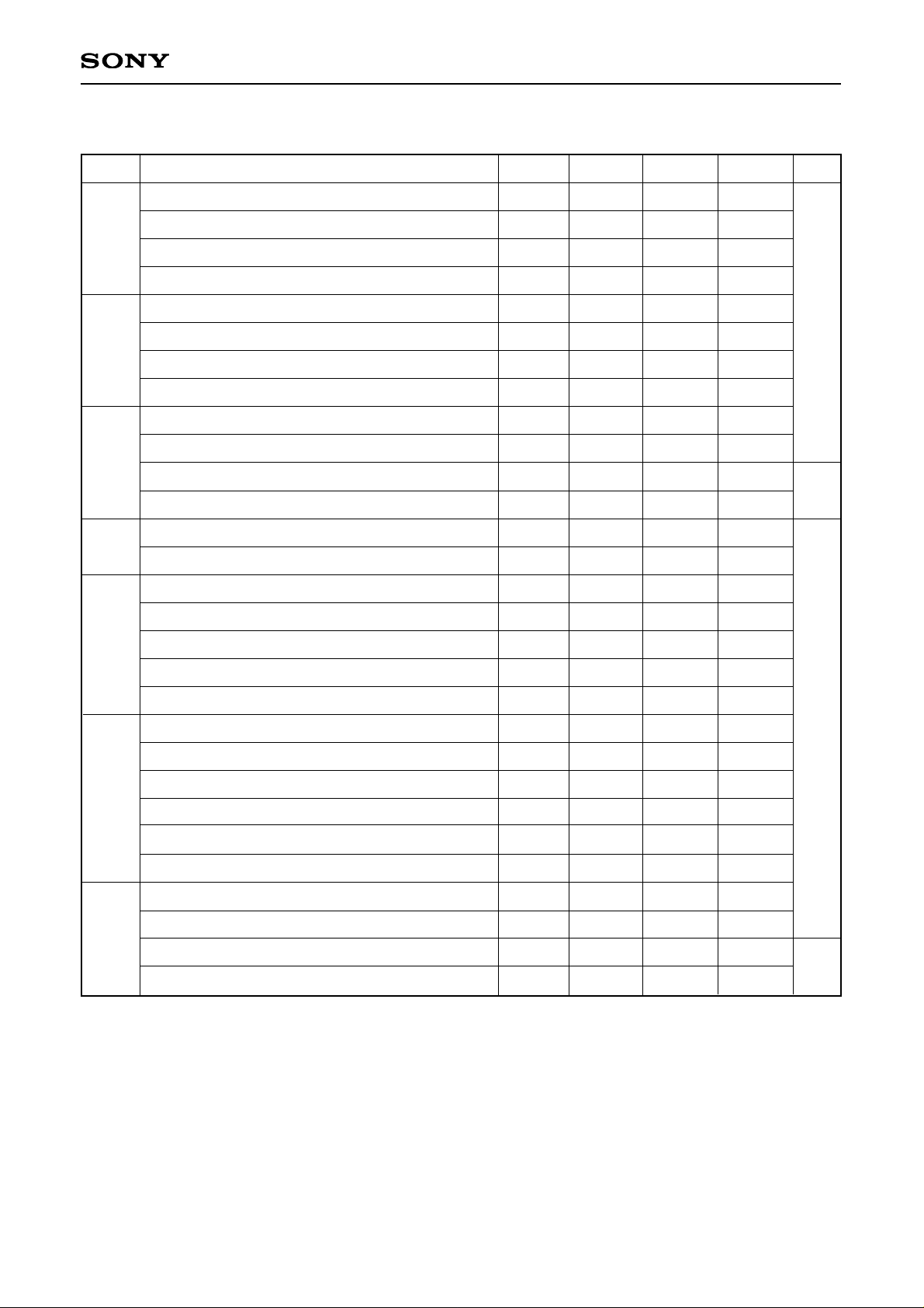
2. Clock timing conditions (Ta = 25°C) (Macintosh16 mode: fHckn = 4.8MHz, fVck = 24.9kHz)
∗4
Hckn means Hck1 and Hck2.
∗5
Blk is the timing during SVGA mode (fHckn = 4.0MHz, fVck = 24.0kHz).
This pulse is positive polarity other than in Macintosh16 mode. Set to L level in Macintosh16 mode.
Hst rise time
Hst fall time
Hst data setup time
Hst data hold time
Hckn rise time
∗4
Hckn fall time
∗4
Hck1 fall to Hck2 rise time
Hck1 rise to Hck2 fall time
Vst rise time
Vst fall time
Vst data setup time
Vst data hold time
Vck rise time
Vck fall time
Enb rise time
Enb fall time
Vck rise/fall to Enb rise time
Horizontal video period end to Enb fall time
Enb fall to Pcg rise time
Pcg rise time
Pcg fall time
Pcg rise to Prg rise time
Pcg fall to Prg fall time
Pcg rise to Vck rise/fall time
Pcg pulse width
Blk rise time
Blk fall time
Blk fall to Vst rise time
Blk pulse width
trHst
tfHst
tdHst
thHst
trHckn
tfHckn
to1Hck
to2Hck
trVst
tfVst
tdVst
thVst
trVck
tfVck
trEnb
tfEnb
toEnb
tdEnb
toPcg
trPcg
tfPcg
toPrgr
toPrgf
toVck
twPcg
trBlk
tfBlk
toVst
twBlk
—
—
70
15
—
—
–15
–15
—
—
5
5
—
—
—
—
400
900
900
—
—
0
200
0
1100
—
—
1
1
—
—
80
25
—
—
0
0
—
—
10
10
—
—
—
—
500
1000
1000
—
—
—
250
1000
1200
—
—
—
—
30
30
90
35
30
30
15
15
100
100
15
15
100
100
100
100
—
—
—
30
30
—
—
1100
1300
100
100
2
—
ns
µs
ns
Item Symbol Min. Typ. Max. Unit
HST
HCK
VST
VCK
ENB
PCG
BLK
∗5
line
Page 8
– 8 –
LCX020BK
∗6
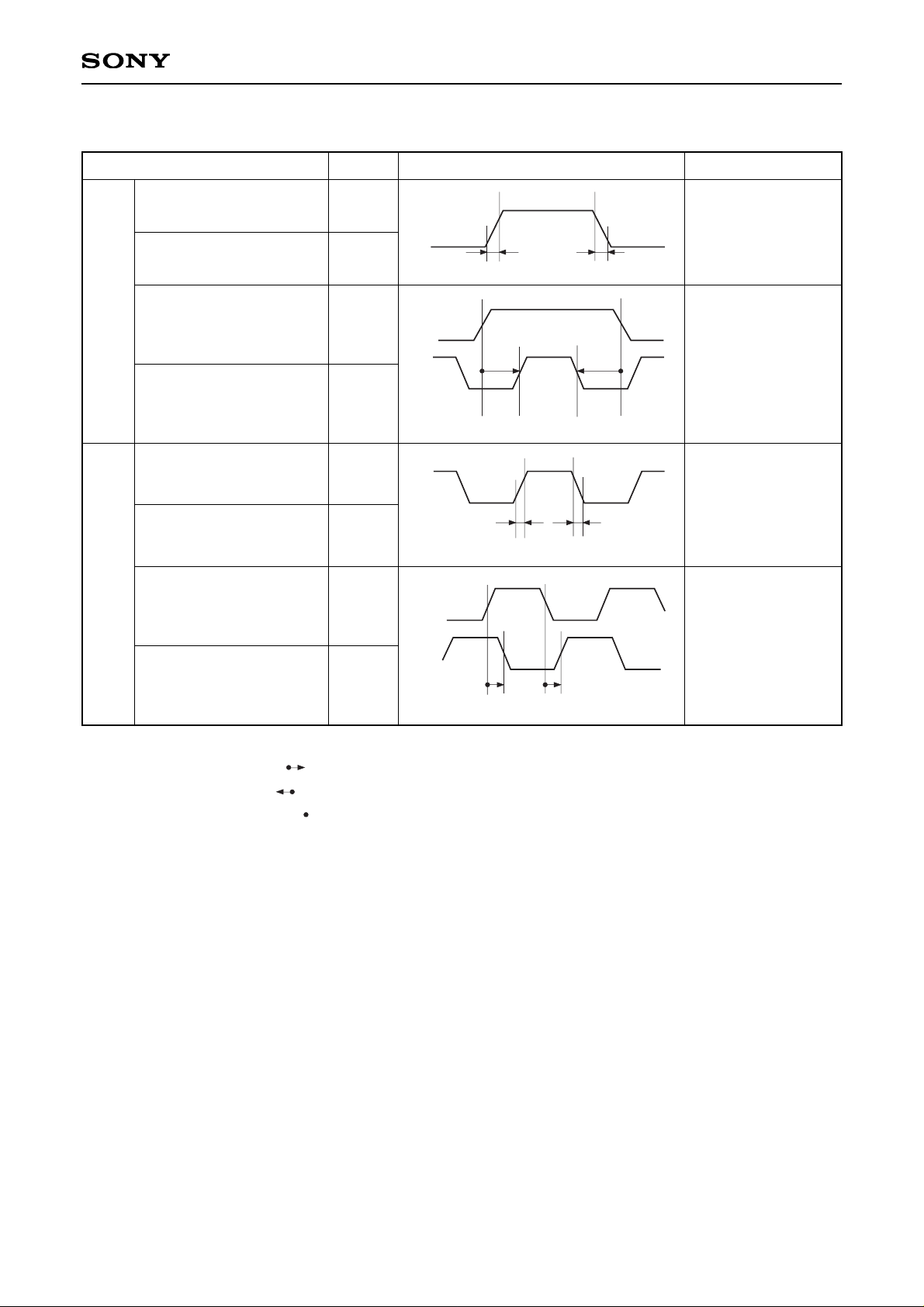
Definitions:
The right-pointing arrow ( ) means +.
The left-pointing arrow ( ) means –.
The black dot at an arrow ( ) indicates the start of measurement.
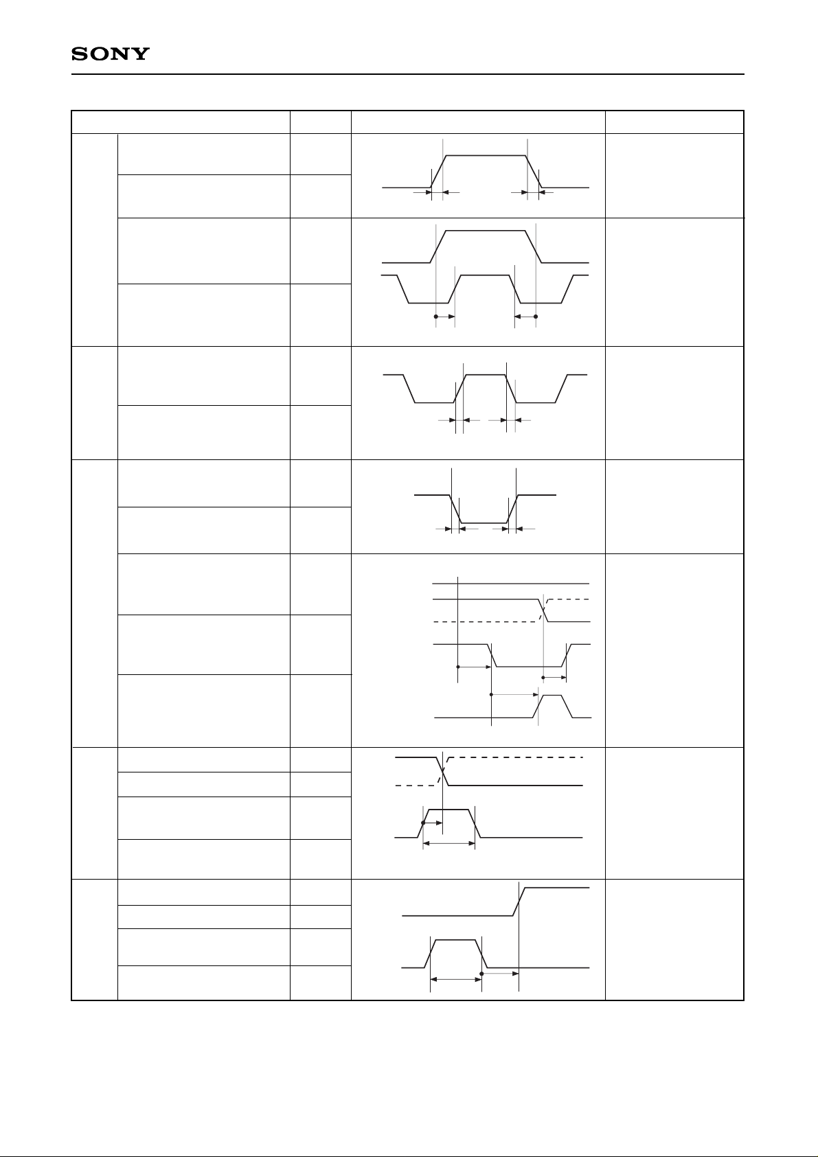
<Horizontal Shift Register Driving Waveform>
Hst rise time
HST
HCK
Hst fall time
Hst data setup time
Hst data hold time
Hckn rise time
∗3
Hckn fall time
∗3
Hck1 fall
to Hck2 rise time
Hck1 rise
to Hck2 fall time
• Hckn
∗3
duty cycle 50%
to1Hck = 0ns
to2Hck = 0ns
• Hckn
∗3
duty cycle 50%
to1Hck = 0ns
to2Hck = 0ns
• Hckn
∗3
duty cycle 50%
to1Hck = 0ns
to2Hck = 0ns
trHst
tfHst
tdHst
thHst
trHckn
tfHckn
to1Hck
to2Hck
Item Symbol Waveform Conditions
90%
10%
10%
90%
Hst
trHst tfHst
50%
50%
∗
6
Hst
Hck1
tdHst thHst
50% 50%
∗
3
Hckn
10%
10%
90%
90%
trHckn tfHckn
50%
50%
∗
6
Hck1
to2Hck to1Hck
50%
50%
Hck2
Page 9
– 9 –
LCX020BK
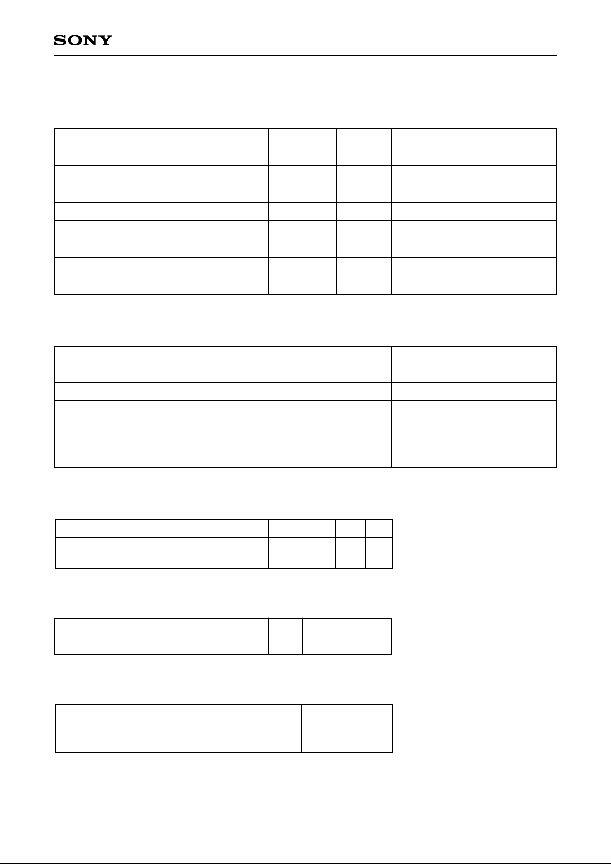
<Vertical Shift Register Driving Waveform>
VCK
ENB
Vck rise time
Vck fall time
Enb rise time
Enb fall time
Vck rise/fall
to Enb rise time
Horizontal video period end
to Enb fall time
trVck
tfVck
trEnb
tfEnb
toEnb
tdEnb
Item Symbol Waveform
Vck
10%
10%
90%
90%
trVckn tfVckn
90%
90%
10%
10%
tfEn trEn
Enb
Enb
50%
50%
50%
toPcg
tdEnb
Vck
∗
6
Horizontal video period
Horizontal blanking period
Pcg
50%
toEnb
PCG
∗7
Pcg rise time
trPcg
Pcg fall time
tfBlk
Pcg rise
to Vck rise/fall time
toVst
Pcg pulse width
twBlk
BLK
Blk rise time
trPcg
Blk fall time
tfPcg
Blk fall to Vst rise time
Blk pulse width
toVck
twBlk
Pcg
50%
50%
50%
twPcg
toVck
Vck
∗
6
Blk
50%
50%
toVst
Vst
∗
6
50%
twBlk
∗7
Input the pulse obtained by taking the OR of the above pulses and BLK to the PCG input pin.
Vst rise time
VST
Vst fall time
Vst data setup time
Vst data hold time
trVst
tfVst
tdVst
thVst
90%
10%
10%
90%
Vst
trVst tfVst
50%
50%
∗
6
Vst
Vck
tdVst thVst
50%
50%
Enb fall to Pcg rise time toPcg
Page 10
– 10 –
LCX020BK
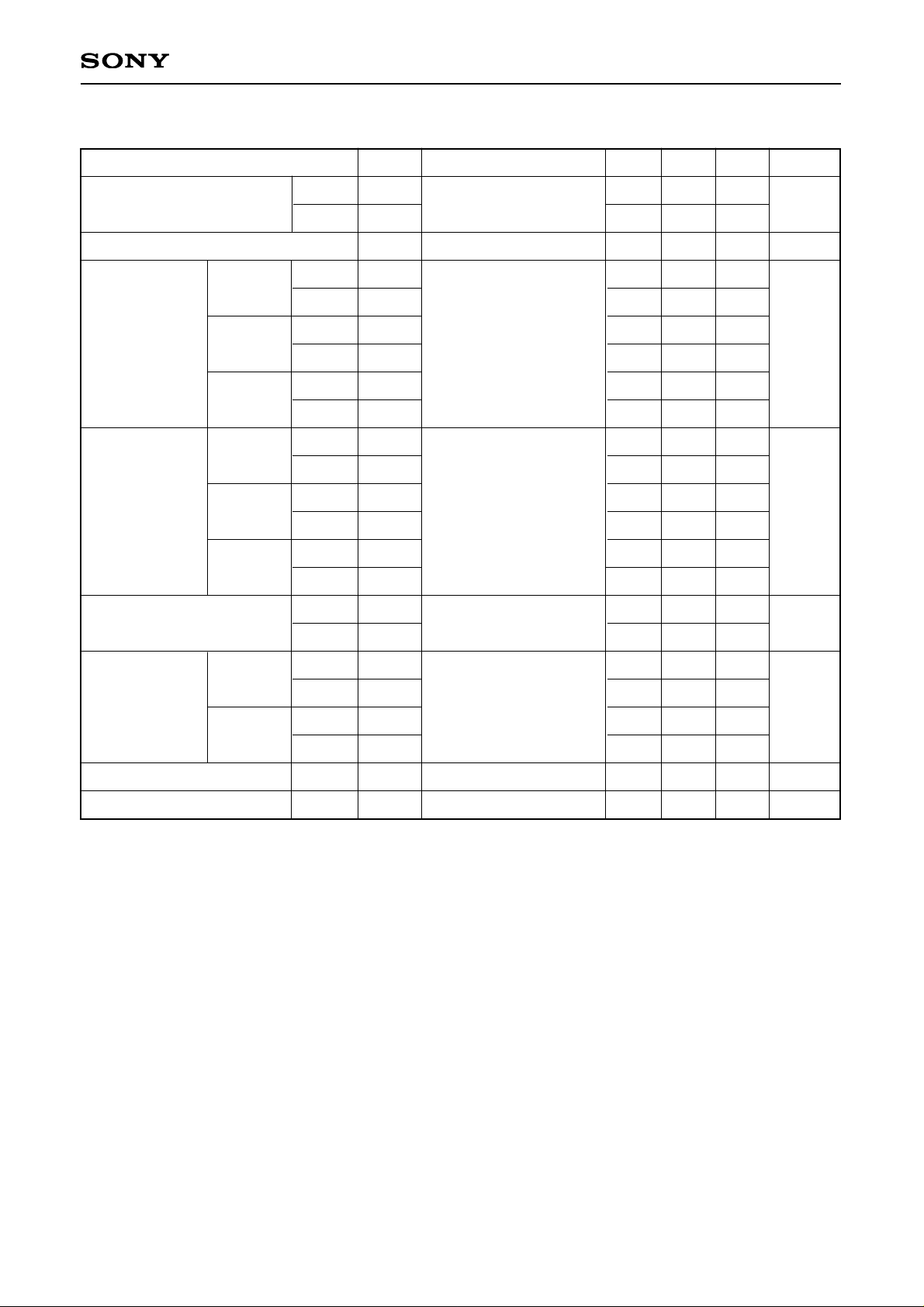
Electrical Characteristics (Ta = 25°C, HVDD = 15.5V, VVDD = 15.5V)
1. Horizontal drivers
Item
Input pin capacitance HCKn
HST
Input pin current HCK1
HCK2
HST
RGT
Video signal input pin capacitance
Current consumption
CHckn
CHst
Csig
IH
HCK1 = GND
HCK2 = GND
HST = GND
RGT = GND
HCKn: HCK1, HCK2 (4.8MHz)
—
—
–500
–1000
–500
–150
—
—
8
8
–110
–350
–180
–30
150
16.0
13
13
—
—
—
—
270
30.0
pF
pF
µA
µA
µA
µA
pF
mA
Symbol Min. Typ. Max. Unit Condition
2. Vertical drivers
Item
Input pin capacitance VCK
VST
Input pin current VCK
PCG, VST, ENB, DWN, BLK,
MODE1, MODE2, MODE3
Current consumption
CVck
CVst
IV
—
—
–1000
–150
—
8
8
–160
–30
3.0
13
13
—
—
5.0
pF
pF
µA
µA
mA
Symbol Min. Typ. Max. Unit Condition
3. Total power consumption of the panel
Item
Total power consumption of the panel
(MAC16)
PWR — 300 600 mW
Symbol Min. Typ. Max. Unit
4. Pin input resistance
Item
Pin – Vss input resistance Rpin 0.4 1 — MΩ
Symbol Min. Typ. Max. Unit
VCK = GND
PCG, VST, ENB, DWN, BLK,
MODE1, MODE2, MODE3 = GND
VCK: (24.9kHz)
5. Uniformity improvement signal input capacitance
Item
Uniformity improvement signal input
capacitance
CPSIGon
7 nF
Symbol Min. Typ. Max. Unit
—
16
Page 11
– 11 –
LCX020BK
Electro-optical Characteristics (Ta = 25°C, NTSC mode)
Item
Contrast ratio
25°C
60°C
X
Y
X
Y
X
Y
25°C
60°C
25°C
60°C
25°C
60°C
R-G
B-G
0°C
25°C
0°C
25°C
60°C
60 min.
CR25
CR60
T
Rx
Ry
Gx
Gy
Bx
By
V90-25
V90-60
V50-25
V50-60
V10-25
V10-60
V50RG
V50BG
ton0
ton25
toff0
toff25
F
YT60
40
40
0.85
0.560
0.300
0.260
0.541
0.120
0.040
0.9
1.0
1.2
1.3
1.9
1.8
—
—
—
—
—
—
—
—
70
70
1.0
0.600
0.360
0.300
0.595
0.148
0.148
1.4
1.6
1.8
1.9
2.4
2.3
–0.10
0.05
20
14
45
35
—
—
—
—
—
0.670
0.410
0.350
0.650
0.187
0.187
2.0
2.2
2.4
2.5
3.0
3.0
0.25
0.45
100
40
150
70
–40
20
1
2
3
4
5
6
7
8
—
%
CIE
standards
V
V
ms
dB
s
Optical transmittance
Chromaticity
R
G
B
V90
V50
V10
ON time
OFF time
V-T
characteristics
Half tone color reproduction
range
Response time
Flicker
Image retention time
Symbol Measurement method Min. Typ. Max. Unit
Page 12
– 12 –
LCX020BK
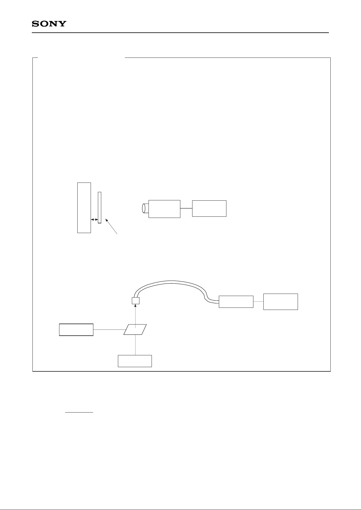
<Electro-optical Characteristics Measurement>
∗
Measurement system II
Light Detector
Optical fiber
LCD panel
Light receptor lens
Drive Circuit
Light Source
Basic measurement conditions
(1) Driving voltage
HVDD = 15.5V, VVDD = 15.5V
VVC = 7.0V, Vcom = 6.6V
(2) Measurement temperature
25°C unless otherwise specified.
(3) Measurement point
One point in the center of the screen unless otherwise specified.
(4) Measurement systems
Two types of measurement system are used as shown below.
(5) Video input signal voltage (Vsig)
Vsig = 7.0 ± VAC [V] (VAC = signal amplitude)
∗
Measurement system I
LCD panel
Luminance
Meter
Measurement
Equipment
Back light: color temperature 6800K ± 700K (25°C)
∗
Back light spectrum (reference) is listed on another page.
Back Light
3.5mm
Measurement
Equipment
1. Contrast Ratio
Contrast Ratio (CR) is given by the following formula (1).
CR = ... (1)
L (White): Surface luminance of the TFT-LCD panel at the input signal amplitude VAC = 0.5V.
L (Black): Surface luminance of the panel at VAC = 4.5V.
Both luminosities are measured by System I.
L (White)
L (Black)
Page 13
– 13 –
LCX020BK
2. Optical Transmittance
Optical Transmittance (T) is given by the following formula (2).
T = × 100 [%] ... (2)
L (White) is the same expression as defined in the "Contrast Ratio" section.
Optical transmittance is measured by System I.
3. Chromaticity
Chromaticity of the panel is measured by System I. Raster modes of each color are defined by the
representations at the input signal amplitude conditions shown in the table below. System I uses x and y of
the CIE standards as the chromaticity here.
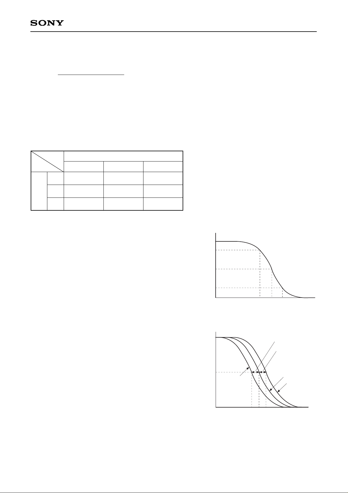
4. V-T Characteristics
V-T characteristics, or the relationship between signal
amplitude and the transmittance of the panel, are
measured by System II by inputting the same signal
amplitude VAC to each input pin. V90, V50, and V10
correspond to each voltage which defines 90%, 50%,
and 10% of transmittance respectively.
5. Half Tone Color Reproduction Range
The half tone color reproduction range of the LCD
panel is characterized by the differences between the
V-T characteristics of R, G and B. The differences of
these V-T characteristics are measured by System II.
System II defines signal voltages of each R, G and B
raster mode which correspond to 50% of transmittance,
V50R, V50G and V50B respectively. V50RG and V50BG
represent the differences between V50R and V50G and
between V50B and V50G, and are given by the following
formulas (3) and (4) respectively.
V50RG = V50R – V50G ... (3)
V50BG = V50B – V50G ... (4)
90
50
10
V
90 V50 V10
VAC – Signal amplitude [V]
Transmittance [%]
Signal amplitudes (VAC) supplied to each input
R input G input B input
Raster
R
G
B
0.5
4.5
4.5
4.5
0.5
4.5
4.5
4.5
0.5
(Unit: V)
100
50
0
V
50R V50B
V50G
VAC – Signal amplitude [V]
Transmittance [%]
V50RG
V50BG
G raster
B raster
R raster
L (White)
Luminance of Back Light
Page 14
– 14 –
LCX020BK
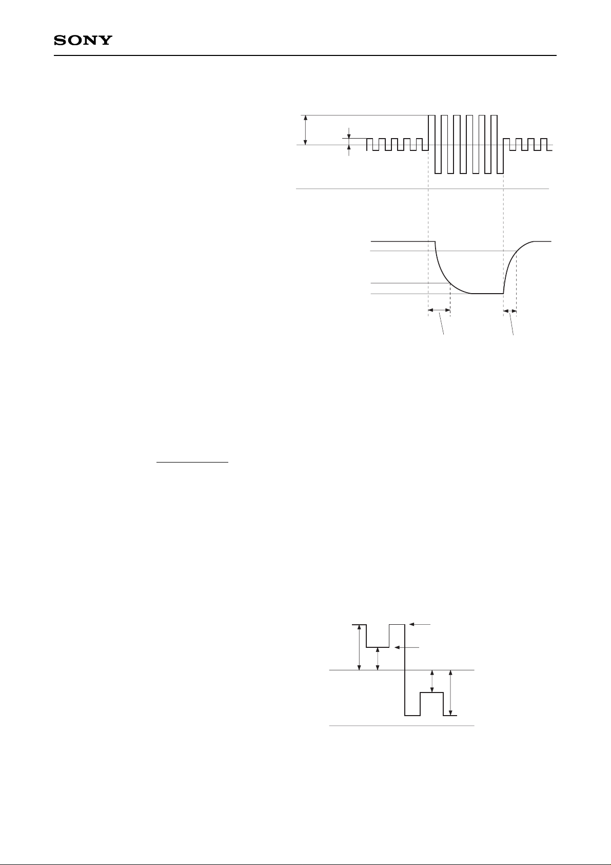
6. Response Time
Response time ton and toff are defined
by formulas (5) and (6) respectively.
ton = t1 – tON ... (5)
toff = t2 – tOFF ... (6)
t1: time which gives 10% transmittance
of the panel.
t2: time which gives 90% transmittance
of the panel.
The relationships between t1, t2, tON
and tOFF are shown in the right figure.
Input signal voltage (Waveform applied to the measured pixels)
4.5V
0.5V
7.0V
0V
Optical transmittance output waveform
100%
90%
10%
0%
tON t1
ton
tOFF t2
toff
7. Flicker
Flicker (F) is given by the formula (7). DC and AC (MAC16/SVGA/VGA/PC98/NTSC: 30Hz, rms, PAL:
25Hz, rms) components of the panel output signal for gray raster∗mode are measured by a DC voltmeter
and a spectrum analyzer in System II.
F [dB] = 20log { } ... (7)
8. Image Retention Time
Image retention time is given by the following procedures.
Apply a monoscope signal to the LCD panel for 60 minutes and then change this signal to the gray scale of
Vsig = 7.0 ± VAC [V] (VAC: 3 to 4V) so as to give the maximum image retention. Hold input signal VAC. The
time for the residual image to disappear gives the image retention time.
∗
Monoscope signal conditions
Vsig = 7.0 ± 4.5 or 7.0 ±2.0 [V]
(shown in the right figure)
Vcom = 6.6V
∗
R, G, B input signal voltage for gray raster mode is given by
Vsig = 7.0 ± V50 [V]
where: V50 is the signal amplitude which gives 50% of
transmittance in V-T curve.
Black level
White level
Vsig waveform
7.0V
0V
4.5V
2.0V
4.5V
2.0V
AC component
DC component
Page 15
– 15 –
LCX020BK
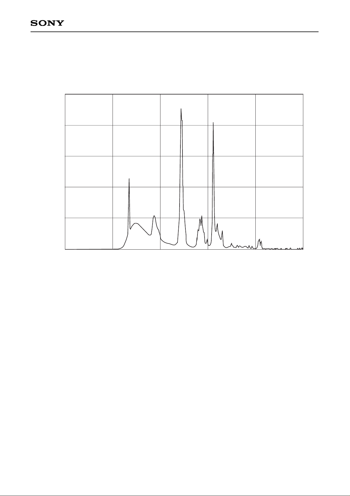
Example of Back Light Spectrum (Reference)
5.000E – 01
A.U.
0.000E + 00
300.00 800.00
Wavelength [nm]
Spectral distribution data
Page 16
– 16 –
LCX020BK
48 dots
2592 dots
48 dots
2496 dots (effective 14.23mm)
628 dots
2 dots
2 dots
624 dots (effective 10.61mm)
Gate SW
Gate SW
Gate SW Gate SWGate SW
Gate SW
G1R1 B1 R6 G6 B6 G1R1 B1 R6 G6 B6
G1R1 B1 R2 G2 B2 R3 G3 R4B3 B4G4 R5 G5 B5 R6 G6 B6
G1R1 B1 R2 G2 B2 R3 G3 R4B3 G4 B6
G1R1 B1 G1R1 B1
B4 R5 G5 B5 R6 G6
R6 G6 B6 R6 G6 B6
G1R1 B1 R6 G6 B6 G1R1 B1 R6 G6 B6
G1R1 B1 R2 G2 B2 R3 G3 R4B3 B4G4 R5 G5 B5 R6 G6 B6
G1R1 B1 R2 G2 B2 R3 G3 R4B3 G4 B6
G1R1 B1 G1R1 B1
B4 R5 G5 B5 R6 G6
R6 G6 B6 R6 G6 B6
G1R1 B1 R6 G6 B6 G1R1 B1 R6 G6 B6
G1R1 B1 R2 G2 B2 R3 G3 R4B3 B4G4 R5 G5 B5 R6 G6 B6
G1R1 B1 R2 G2 B2 R3 G3 R4B3 G4 B6
G1R1 B1 G1R1 B1
B4 R5 G5 B5 R6 G6
R6 G6 B6 R6 G6 B6
G1R1 B1 R6 G6 B6 G1R1 B1 R6 G6 B6
G1R1 B1 R2 G2 B2 R3 G3 R4B3 B4G4 R5 G5 B5 R6 G6 B6
G1R1 B1 R2 G2 B2 R3 G3 R4B3 G4 B6
G1R1 B1 G1R1 B1
B4 R5 G5 B5 R6 G6
R6 G6 B6 R6 G6 B6
G1R1 B1 R6 G6 B6 G1R1 B1 R6 G6 B6
G1R1 B1 R2 G2 B2 R3 G3 R4B3 B4G4 R5 G5 B5 R6 G6 B6
G1R1 B1 R2 G2 B2 R3 G3 R4B3 G4 B6
G1R1 B1 G1R1 B1
B4 R5 G5 B5 R6 G6
R6 G6 B6 R6 G6 B6
G1R1 B1 R6 G6 B6 G1R1 B1 R6 G6 B6
G1R1 B1 R2 G2 B2 R3 G3 R4B3 B4G4 R5 G5 B5 R6 G6 B6
G1R1 B1 R2 G2 B2 R3 G3 R4B3 G4 B6
G1R1 B1 G1R1 B1
B4 R5 G5 B5 R6 G6
R6 G6 B6 R6 G6 B6
G1R1 B1 R6 G6 B6 G1R1 B1 R6 G6 B6
G1R1 B1 R2 G2 B2 R3 G3 R4B3 B4G4 R5 G5 B5 R6 G6 B6
G1R1 B1 R2 G2 B2 R3 G3 R4B3 G4 B6
G1R1 B1 G1R1 B1
B4 R5 G5 B5 R6 G6
R6 G6 B6 R6 G6 B6
G1R1 B1 R6 G6 B6 G1R1 B1 R6 G6 B6
G1R1 B1 R2 G2 B2 R3 G3 R4B3 B4G4 R5 G5 B5 R6 G6 B6
G1R1 B1 R2 G2 B2 R3 G3 R4B3 G4 B6
G1R1 B1 G1R1 B1
B4 R5 G5 B5 R6 G6
R6 G6 B6 R6 G6 B6
G1R1 B1 R6 G6 B6 G1R1 B1 R6 G6 B6
G1R1 B1 R2 G2 B2 R3 G3 R4B3 B4G4 R5 G5 B5 R6 G6 B6
G1R1 B1 R2 G2 B2 R3 G3 R4B3 G4 B6
G1R1 B1 G1R1 B1
B4 R5 G5 B5 R6 G6
R6 G6 B6 R6 G6 B6
G1R1 B1 R6 G6 B6 G1R1 B1 R6 G6 B6
G1R1 B1 R2 G2 B2 R3 G3 R4B3 B4G4 R5 G5 B5 R6 G6 B6
G1R1 B1 R2 G2 B2 R3 G3 R4B3 G4 B6
G1R1 B1 G1R1 B1
B4 R5 G5 B5 R6 G6
R6 G6 B6 R6 G6 B6
Active area
Photo-
shielding
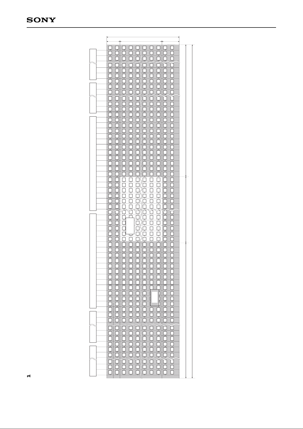
1. Dot Arrangement
RGB dots are arranged in a stripe pattern. The shaded area is used for the dark border around the display.
Page 17
– 17 –
LCX020BK
2. LCD Panel Operations
[Description of basic operations]
• A vertical driver, which consists of vertical shift registers, enable-gates and buffers, applies a selected pulse
to every 624 gate lines sequentially in every single horizontal scanning period. (in Macintosh16 mode)
• A horizontal driver, which consists of horizontal shift registers, gates and CMOS sample-and-hold circuits,
applies selected pulses to every 2496 signal electrodes sequentially in a single horizontal scanning period.
These pulses are used to supply the sampled video signal to the row signal lines.
• Vertical and horizontal shift registers address one pixel, and then Thin Film Transistors (TFTs; two TFTs for
one dot) turn on to apply a video signal to the dot. The same procedures lead to the entire 2496 × 832 dots to
display a picture in a single vertical scanning period.
• The data and video signals shall be input with polarity-inverted system in every horizontal cycle.
[Description of operating mode]
The LCD panel can change the angle of view by displaying a black frame to support various signal systems.
The angle of view is switched by MODE1, 2 and 3. However, the picture center does not change. The angle of
view mode settings are shown below.
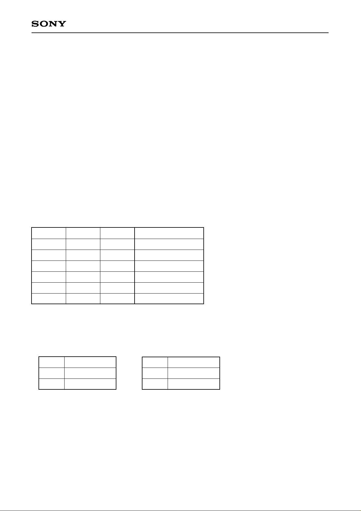
MODE1 MODE2 MODE3 Display mode
L
L
L
L
H
H
L
L
H
H
L
L
L
H
L
H
L
H
Macintosh16: 832 × 624
SVGA: 800 × 600
PAL: 762 × 572
VGA/NTSC: 640 × 480
PC98: 640 × 400
WIDE: 832 × 480
The LCD panel has the following functions to easily apply to various uses, as well as various signal systems.
• Right/left inverse mode
• Up/down inverse mode
These modes are controlled by two signals (RGT and DWN). The right/left and up/down mode settings are
shown in the tables below.
Right/left and up/down mean the direction when the Pin 1 marking is located at the right side with the pin block
facing upward.
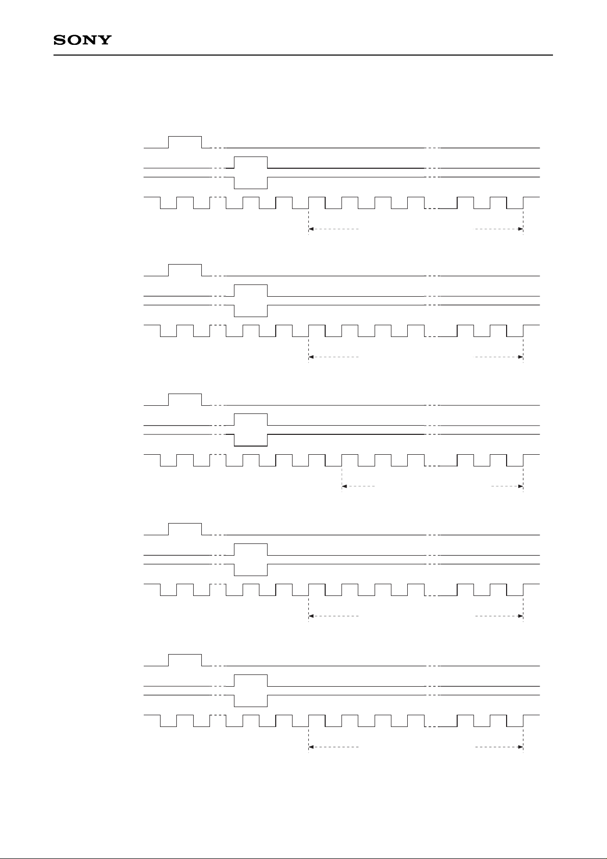
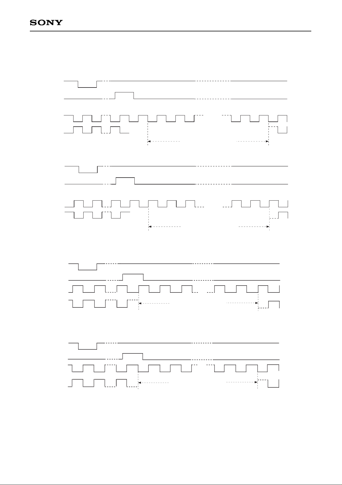
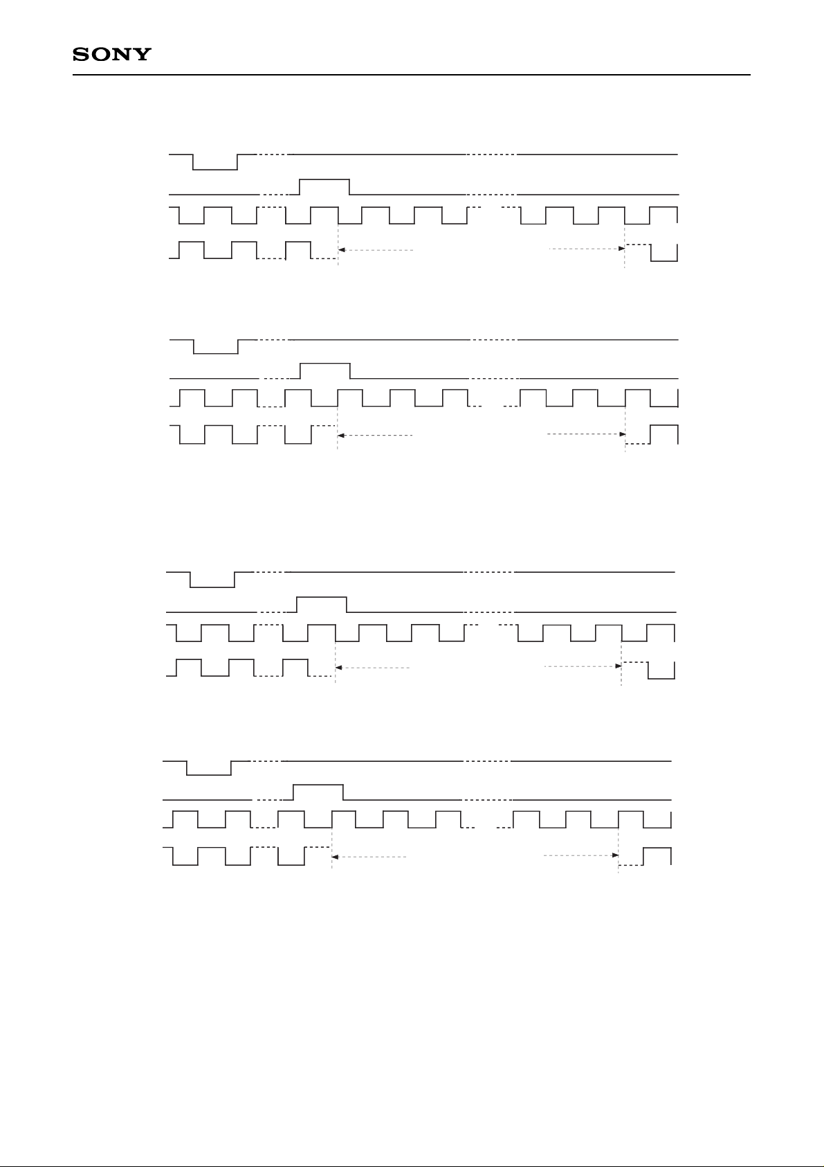
Since the display area is located in the center of the panel in each mode, the start pulse, clock phase and
polarity for both the H and V systems must be varied. The phase relationship between the start pulse and the
clock for each mode is shown on the following pages.
RGT Mode
Right scan
Left scan
H
L
DWN Mode
Down scan
Up scan
H
L
Page 18
– 18 –
LCX020BK
(1) Vertical direction display cycle
(1.1) Macintosh 16
VD
VST (DWN = H)
VST (DWN = L)
VCK
1 32 4
621 623622 624
Vertical display cycle 624H
(1.2) SVGA
VD
VST (DWN = H)
VST (DWN = L)
VCK
1 32 4
597 599598 600
Vertical display cycle 600H
(1.3) PAL
VD
VST (DWN = H)
VST (DWN = L)
VCK
1 32 4
569 571570 572
Vertical display cycle 572H
(1.4) VGA/NTSC, WIDE
VD
VST (DWN = H)
VST (DWN = L)
VCK
1 32 4
477 479478 480
Vertical display cycle 480H
(1.5) PC98
VD
VST (DWN = H)
VST (DWN = L)
VCK
1 32 4
397 399398 400
Vertical display cycle 400H
Page 19
– 19 –
LCX020BK
(2) Horizontal direction display cycle
(2.1.1) Macintosh 16, WIDE, RGT = H
HD
HST
HCK1
HCK2
1 32 4 139 140137 138
Horizontal display cycle
(2.1.2) Macintosh 16, WIDE, RGT = L
1 32 4 139 140137 138
HD
HST
HCK1
HCK2
Horizontal display cycle
(2.2.1) SVGA, RGT = H
HST
HCK1
HCK2
HD
1 2 3 4 131 132 133 134
Horizontal display cycle
(2.2.2) SVGA, RGT = L
HST
HCK1
1 2 3 4 131 132 133 134
HCK2
HD
Horizontal display cycle
Page 20
– 20 –
LCX020BK
(2.3.1) PAL, RGT = H
1 2 3 4
HST
HCK1
125 126 127 128
HCK2
HD
Horizontal display cycle
(2.3.2) PAL, RGT = L
HST
HCK1
1 2 3 4 125 126 127 128
HCK2
HD
Horizontal display cycle
(2.4.1) VGA/NTSC/PC98, RGT = H
HST
HCK1
105 106 107 108
HCK2
HD
1 2 3 4
Horizontal display cycle
(2.4.2) VGA/NTSC/PC98, RGT = L
HST
HCK1
1 2 3 4 105 106 107 108
HCK2
HD
Horizontal display cycle
Page 21
– 21 –
LCX020BK
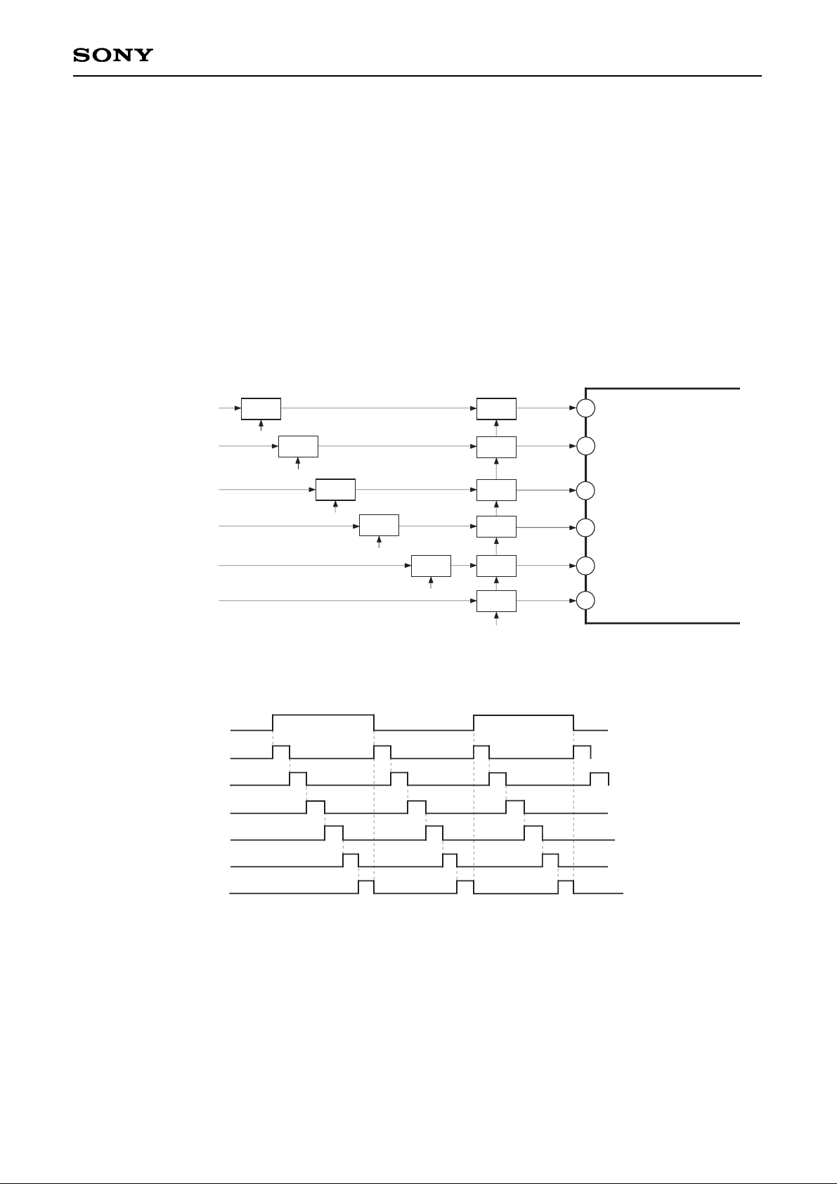
3. 18-dot Simultaneous Sampling
The horizontal shift register performs SIGR1 to SIGR6, SIGG1 to SIGG6 and SIGB1 to SIGB6 signal sampling
simultaneously, which requires phase matching between each signal to prevent the horizontal resolution from
deteriorating. Phase matching by an external signal delaying circuit is needed before applying video signals to
the LCD panel.
The block diagram of the delaying procedure using the sample-and-hold method is as follows. The following
phase relationship diagram indicates the phase setting for right-direction scanning (RGT = High level). For leftdirection scanning (RGT = Low level), the phase settings should be inverted for the SIGR1 to SIGR6, SIGG1 to
SIGG6 and SIGB1 to SIGB6 signals.
S/H
CK1
CK2
LCX020BK
CK3
CK4
CK5
S/H
S/H
S/H
S/H
S/H
CK6
S/H
S/H
S/H
S/H
S/H
SIGR1, SIGG1, SIGB1
SIGR2, SIGG2, SIGB2
SIGR3, SIGG3, SIGB3
SIGR4, SIGG4, SIGB4
SIGR5, SIGG5, SIGB5
SIGR6, SIGG6, SIGB6
SIGR1, SIGG1, SIGB1
SIGR2, SIGG2, SIGB2
SIGR3, SIGG3, SIGB3
SIGR4, SIGG4, SIGB4
SIGR5, SIGG5, SIGB5
SIGR6, SIGG6, SIGB6
HCKn
CK1
CK3
CK5
CK2
CK4
CK6
<Phase relationship of delaying sample-and-hold pulses> (right-direction scanning)
Page 22
– 22 –
LCX020BK
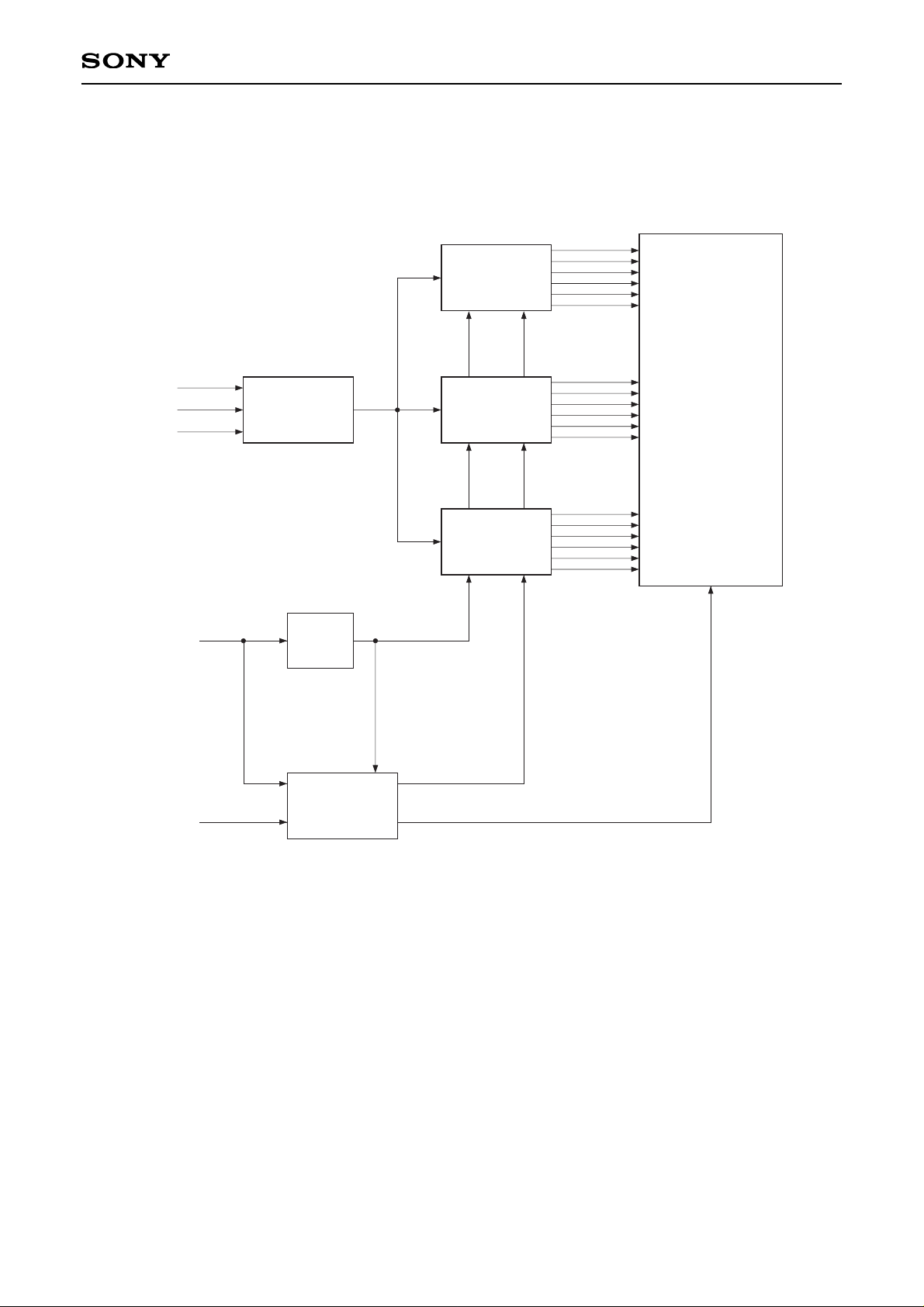
Display System Block Diagram
An example display system configuration is shown below.
CXA2111R
CXA2112R
CXA2112R
CXA2112R
PLL
CXD3500R
LCX020BK
TIMING PULSE
FRP
MCK
HSYNC
VSYNC
R
G
B
R
G
B
Page 23

– 23 –
LCX020BK
Notes on Handling
(1) Static charge prevention
Be sure to take the following protective measures. TFT-LCD panels are easily damaged by static charges.
a) Use non-chargeable gloves, or simply use bare hands.
b) Use an earth-band when handling.
c) Do not touch any electrodes of a panel.
d) Wear non-chargeable clothes and conductive shoes.
e) Install conductive mats on the working floor and working table.
f) Keep panels away from any charged materials.
g) Use ionized air to discharge the panels.
(2) Protection from dust and dust
a) Operate in a clean environment.
b) When delivered, panel surface (Polarizer) is covered by a protective sheet. Peel off the protective sheet
carefully so as not to damage the panel.
c) Do not touch the polarizer surface. The surface is easily scratched. When cleaning, use a clean-room
wiper with isopropyl alcohol. Be careful not to leave a stain on the surface.
d) Use ionized air to blow dust off the polarizer.
(3) Other handling precautions
a) Do not twist or bend the flexible PC board especially at the connecting region because the board is
easily deformed.
b) Do not drop the panel.
c) Do not twist or bend the panel or panel frame.
d) Keep the panel away from heat sources.
e) Do not dampen the panel with water or other solvents.
f) Avoid storing or using the panel at a high temperature or high humidity, which may result in panel
damages.
Page 24
– 24 –
LCX020BK
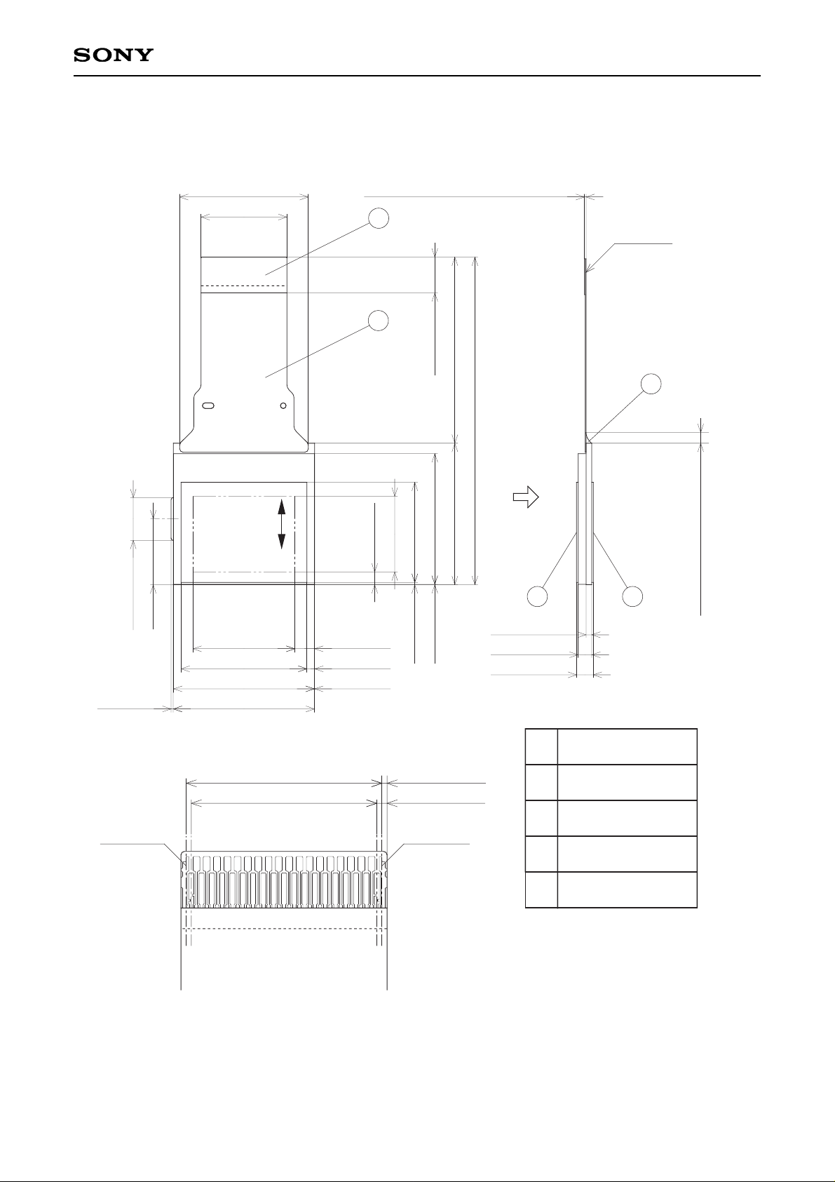
Package Outline Unit: mm
Thickness of the connector
0.2 ± 0.03
Active Area
Polarizing Axis
electrode
18.0 ± 0.3
12.0 ± 0.05
0.8 ± 0.1
1.9 ± 0.3
2.33 ± 0.4
2.761 ± 0.1
1.075 ± 0.3
0.05 ± 0.3
(14.227)
17.6 ± 0.3
19.65 ± 0.15
19.75 ± 0.15
0.3 ± 0.3
6 ± 3
9 ± 3
(10.608)
14.0 ± 0.3
1.754 ± 0.1
18.25 ± 0.15
19.75 ± 0.15
47.75 ± 0.9
(26.0)
5.0 ± 0.3
1.5 ± 1.0
0.3 ± 0.3
0.05 ± 0.3
Reinforcing material
Incident
light
1
4
3
2
electrode (enlarged)
PIN1
PIN 39
0.3 ± 0.07
P 0.6 ± 0.02 × 19 = 11.4 ± 0.03
weight 2g
Description
Reinforcing board
Reinforcing material
Polarizing film
F P C
No
1
2
3
4
0.6 ± 0.07
P 0.6 ± 0.02 × 18 = 10.8 ± 0.03
4
 Loading...