

Page 1
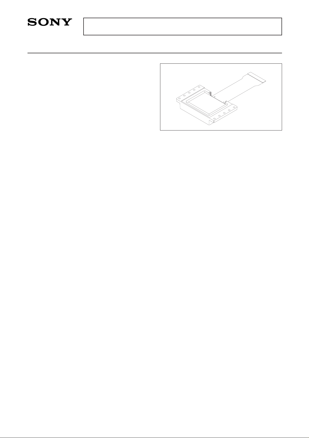
Description
The LCX019AM is a 3.4cm diagonal active matrix
TFT-LCD panel addressed by polycrystalline silicon
super thin film transistors with built-in peripheral
driving circuit. This panel allows full-color
representation without color filters through the use of
a microlens.
This panel has an aspect ratio of 4:3 and supports
NTSC/PAL display.
This panel has a polysilicon TFT high-speed
scanner and built-in function to display images
up/down and/or right/left inverse. The built-in 5V
interface circuit leads to lower voltage of timing and
control signals.
Features
• The number of active dots: 576,000 (1.32-inch; 3.4cm in diagonal)
• Horizontal resolution: 600TV lines
• Effective aperture ratio: 70% (reference value)
• High contrast ratio with normally white mode: 200 (typ.)
• Built-in H and V drivers (built-in input level conversion circuit, 5V driving possible)
• Supports NTSC
(PAL mode also available through conversion of scanned dot numbers by an external IC)
• Up/down and/or right/left inverse display function
Element Structure
• Dots: 1199.5 (H) × 480 (V) = 575,760
• Built-in peripheral driver using polycrystalline silicon super thin film transistors.
Applications
Liquid crystal projectors, etc.
– 1 –
LCX019AM
E97106A94-PS
3.4cm (1.32-inch) LCD Panel (with microlens)
Sony reserves the right to change products and specifications without prior notice. This information does not convey any license by
any implication or otherwise under any patents or other right. Application circuits shown, if any, are typical examples illustrating the
operation of the devices. Sony cannot assume responsibility for any problems arising out of the use of these circuits.
For the availability of this product, please contact the sales office.
Page 2
– 2 –
LCX019AM
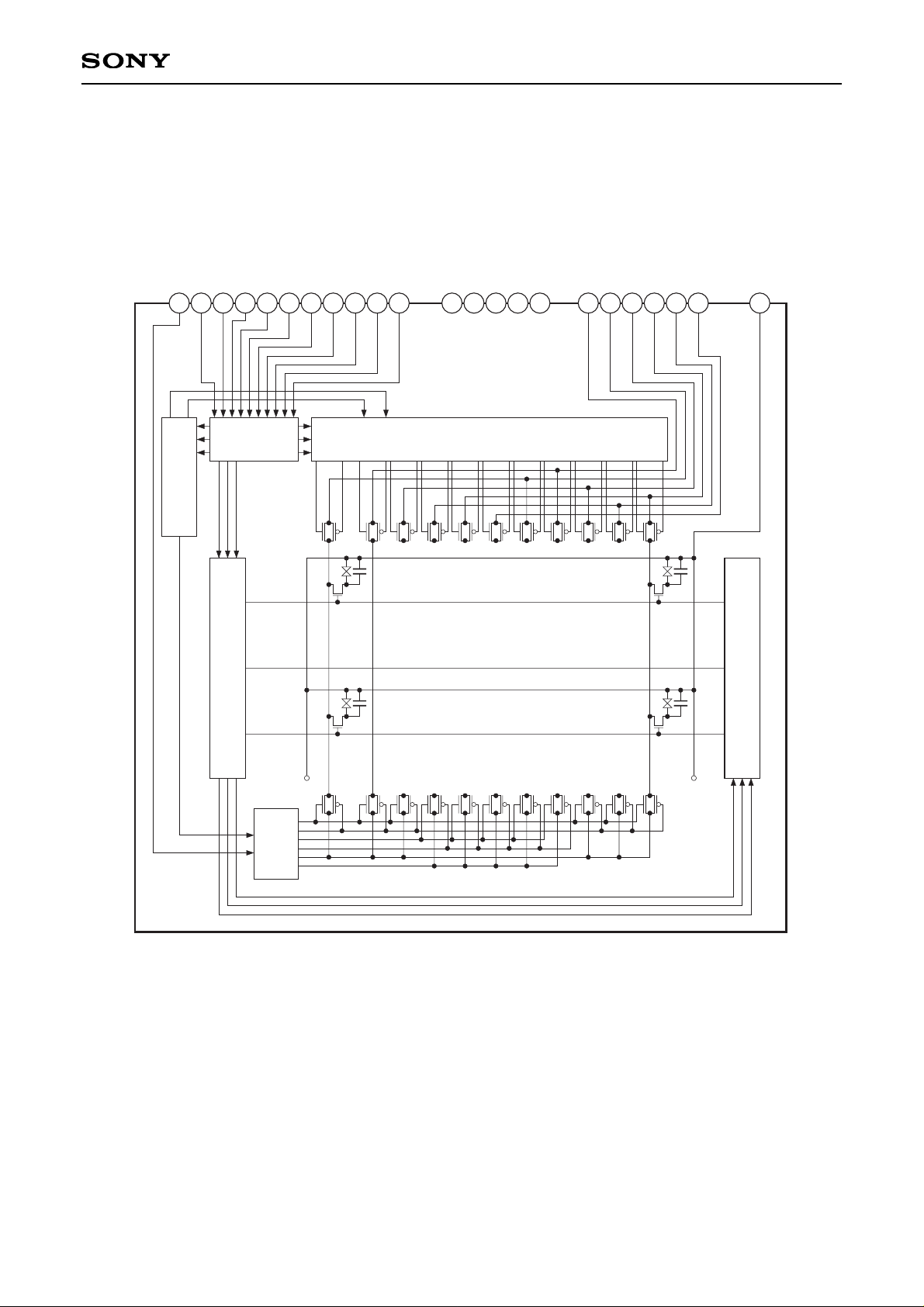
Block Diagram
Mode Controller
Level
Shifter
Bi-directional H Driver
Bi-directional V Driver
Bi-directional V Driver
2
3
4
5
6
7
8
9
10
11
12
13
14 15
16
17
18
19
20
21
22
23
1
VCOM
Precharge
Controller
PSIG
HST
HCK1
HCK2
N.C.
RGT
VST
VCK
PCG
DWN
ENB
AV
DD
HV
DD
VV
DD
V
SS
V
SS
G
SIG6 (B2)
SIG5 (R2)
SIG4 (G2)
SIG3 (B1)
SIG2 (R1)
SIG1 (G1)
COM
Page 3
– 3 –
LCX019AM
Absolute Maximum Ratings (VSS = 0V)
• H driver supply voltage HVDD –1.0 to +20 V
• V driver supply voltage VVDD –1.0 to +20 V
• Analog block drive supply voltage AVDD –1.0 to +20 V
• Common pad voltage COM –1.0 to +17 V
• H shift register input pin voltage HST, HCK1, HCK2 –1.0 to +17 V
RGT
• V shift register input pin voltage VST, VCK, PCG –1.0 to +17 V
ENB, DWN
• Video signal input pin voltage SIG1, SIG2, SIG3, SIG4 –1.0 to +15 V
SIG5, SIG6, PSIG
• Operating temperature Topr –10 to +70 °C
• Storage temperature Tstg –30 to +85 °C
Operating Conditions (VSS = 0V)
• Supply voltage
HVDD 13.5 ± 0.3 V
VVDD 13.5 ± 0.3 V
AVDD 15.5 ± 0.3 V
• Input pulse voltage (Vp-p of all input pins except video signal and side black signal input pins)
Vin 5.0 ± 0.5 V
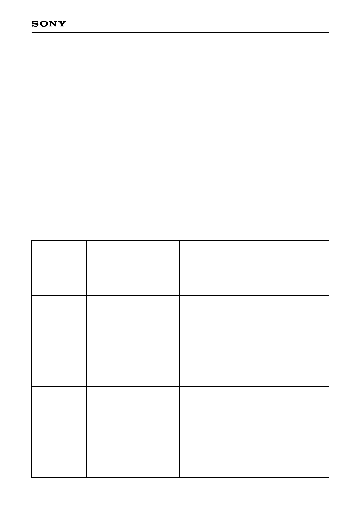
Pin Description
Pin
No.
1
2
3
4
5
6
7
8
9
10
11
12
COM
VSSG
PSIG
SIG1 (G1)
SIG2 (R1)
SIG3 (B1)
SIG4 (G2)
SIG5 (R2)
SIG6 (B2)
AVDD
HVDD
N.C.
13
14
15
16
17
18
19
20
21
22
23
24
RGT
HST
HCK1
HCK2
VSS
ENB
VCK
VST
DWN
PCG
VVDD
TEST
Drive direction pulse for H shift
register (H: normal, L: reverse)
Start pulse for H shift register
drive
Clock pulse for H shift register
drive
Clock pulse for H shift register
drive
GND (H, V drivers)
Enable pulse for gate selection
Clock pulse for V shift register
drive
Start pulse for V shift register
drive
Drive direction pulse for V shift
register (H: normal, L: reverse)
Improvement pulse (2) for
uniformity
Power supply for V driver
Test; Open
Common voltage of panel
Analog block GND
Improvement pulse for uniformity
Video signal 1 (G) to panel
Video signal 2 (R) to panel
Video signal 3 (B) to panel
Video signal 4 (G) to panel
Video signal 5 (R) to panel
Video signal 6 (B) to panel
Analog block power supply
Power supply for H driver
Symbol Description
Pin
No.
Symbol Description
Page 4

– 4 –
LCX019AM
Input Equivalent Circuit
To prevent static charges, protective diodes are provided for each pin except the power supply. In addition,
protective resistors are added to all pins except video signal input. All pins are connected to VSS with a high
resistance of 1MΩ (typ.). The equivalent circuit of each input pin is shown below: (The resistor value: typ.)
Input
LC
Level conversion circuit
(single-phase input)
2.5kΩ2.5kΩ
VV
DD
Input
Level conversion circuit
(single-phase input)
250Ω250Ω
HV
DD
Input
Level conversion circuit
(single-phase input)
2.5kΩ2.5kΩ
HV
DD
Input
HV
DD
250Ω
250Ω
250Ω
250Ω
Level conversion circuit
(2-phase input)
Input
HV
DD
Signal line
(1) SIG1, SIG2, SIG3, SIG4, SIG5, SIG6, PSIG
(2) HCK1, HCK2
(3) RGT
(4) HST
(5) PCG, VCK
(6) VST, ENB, DWN
(7) COM
1MΩ
Input
1MΩ
1MΩ
1MΩ
1MΩ
Level conversion circuit
(single-phase input)
250Ω250Ω
VV
DD
Input
1MΩ
1MΩ
1MΩ
VVDD
VSS VSS
VSS
VSS
VSS
VSS
VSS
VSS
Page 5
– 5 –
LCX019AM
Input Signals
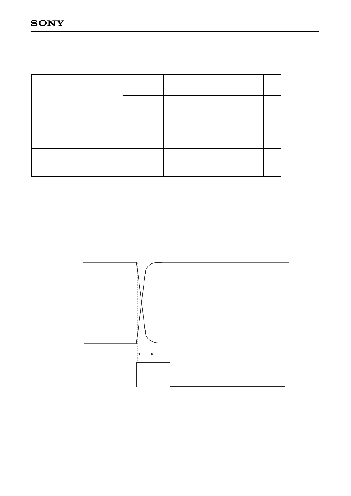
1. Input signal voltage conditions (Vss = 0V)
Item
H driver input voltage
RGT, HST, HCK1, HCK2
(Low)
(High)
(Low)
(High)
VHIL
VHIH
VVIL
VVIH
VVC
Vsig
Vcom
Vpsig
–0.5
4.5
–0.5
4.5
6.8
VVC – 4.5
VVC – 0.3
VVC ± 3.4
0.0
5.0
0.0
5.0
7.0
—
VVC – 0.2
VVC ± 3.5
0.3
5.5
0.3
5.5
7.2
VVC + 4.5
VVC – 0.1
VVC ± 3.6
V
V
V
V
V
V
V
V
V driver input voltage
ENB, VCK, PCG, VST, DWN
Video signal center voltage
Video signal input range∗1(SIG1 to 6)
Common voltage of panel
∗2
Uniformity improvement signal input
(PSIG)
∗3
Symbol Min. Typ. Max. Unit
∗1
Video input signal shall be symmetrical to VVC.
∗2
Common voltage of the panel shall be adjusted to VVC – 0.2 V.
∗3
The uniformity improvement signal PSIG shall be input with the same polarity as video signals SIG1 to 6
and symmetrically with respect to VVC. Also, the PSIG rise and fall shall be synchronized with the PCG
pulse rise and the time between the rise trPSIG and fall tfPSIG shall be kept to 800ns or less. (See the
figure below.)
Uniformity Improvement Signal PSIG Input Waveform
Level Conversion Circuit
The LCX019AM has a built-in level conversion circuit in the clock input unit on the panel. The input signal level
increases to HVDD or VVDD. The VCC of external ICs are applicable to 5 ± 0.5V.
trPSIG
tfPSIG
VVC
PSIG
PCG
90%
10%
Page 6
– 6 –
LCX019AM
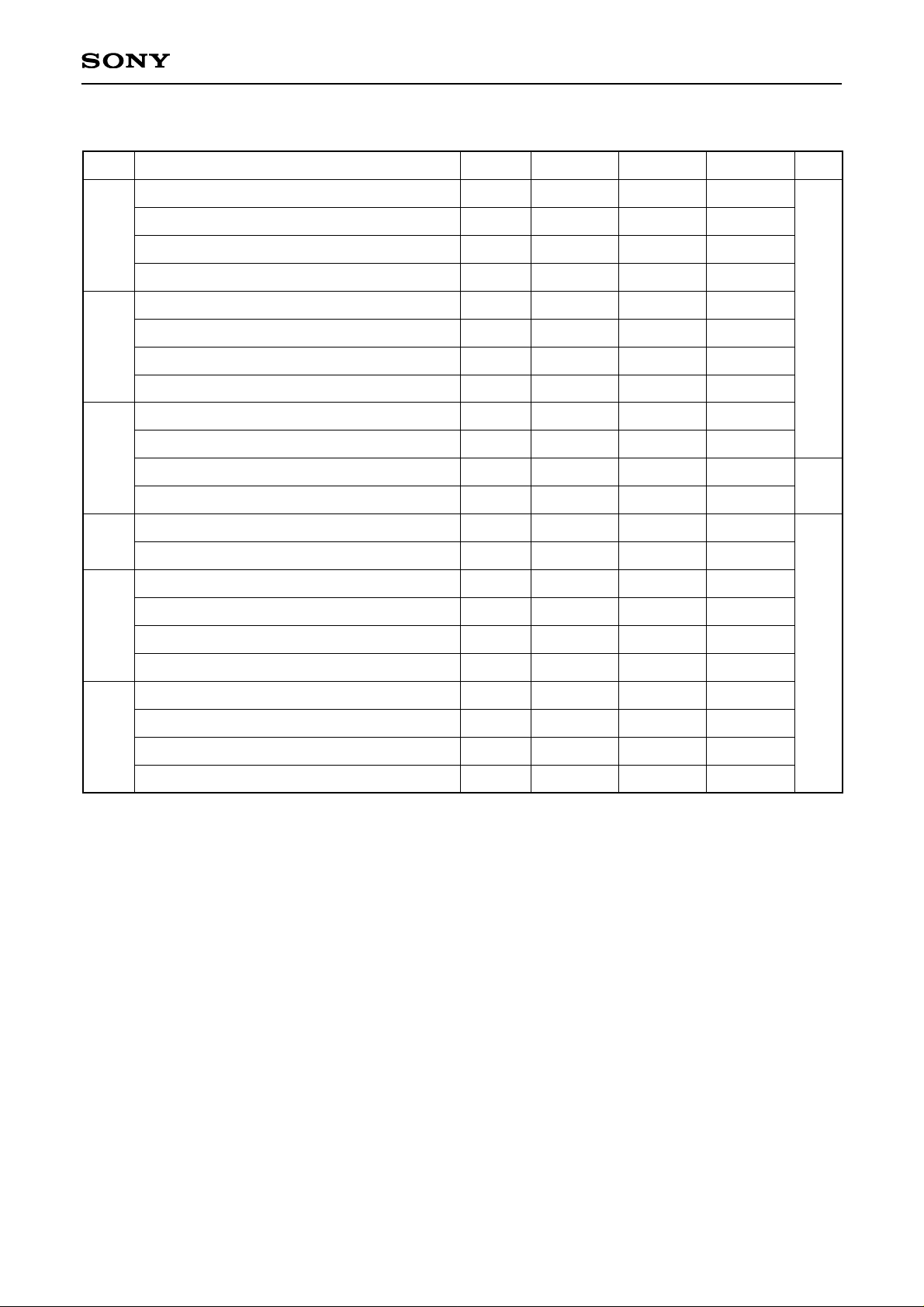
2. Clock timing conditions (Ta = 25°C) (fHCKn = 3.82MHz, fVCK = 15.7kHz)
Hst rise time
Hst fall time
Hst data set-up time
Hst data hold time
Hckn∗4rise time
Hckn∗4fall time
Hck1 fall to Hck2 rise time
Hck1 rise to Hck2 fall time
Vst rise time
Vst fall time
Vst data set-up time
Vst data hold time
Vck rise time
Vck fall time
Enb rise time
Enb fall time
Vck rise/fall to Enb rise time
Enb pulse width
Pcg rise time
Pcg fall time
Pcg fall to Vck rise/fall time
Pcg pulse width
trHst
tfHst
tdHst
thHst
trHckn
tfHckn
to1Hck
to2Hck
trVst
tfVst
tdVst
thVst
trVck
tfVck
trEnb
tfEnb
tdEnb
twEnb
trPcg
tfPcg
toVck
twPcg
—
—
–15
116
—
—
–15
–15
—
—
5
5
—
—
—
—
350
3450
—
—
250
1750
—
—
0
131
—
—
0
0
—
—
15
15
—
—
—
—
400
3500
—
—
300
1800
30
30
15
146
30
30
15
15
100
100
25
25
100
100
100
100
450
3550
20
20
350
1850
ns
µs
ns
Item Symbol Min. Typ. Max. Unit
HST
HCK
VST
VCK
ENB
PCG
∗4
Hckn means Hck1 and Hck2.
Page 7
– 7 –
LCX019AM
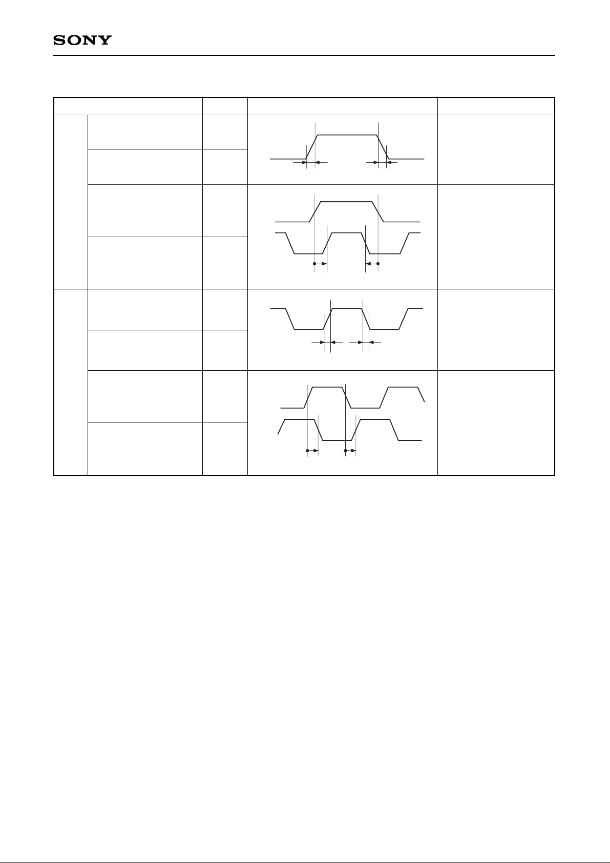
<Horizontal Shift Register Driving Waveform>
Hst rise time
HST
HCK
Hst fall time
Hst data set-up time
Hst data hold time
Hckn∗4rise time
Hckn∗4fall time
Hck1 fall to Hck2 rise
time
Hck1 rise to Hck2 fall
time
• Hckn
∗4
duty cycle 50%
to1Hck = 0ns
to2Hck = 0ns
• Hckn
∗4
duty cycle 50%
to1Hck = 0ns
to2Hck = 0ns
• Hckn
∗4
duty cycle 50%
to1Hck = 0ns
to2Hck = 0ns
trHst
tfHst
tdHst
thHst
trHckn
tfHckn
to1Hck
to2Hck
Item Symbol Waveform Conditions
90%
10%
10%
90%
Hst
trHst tfHst
50%
50%
∗
5
Hst
Hck1
tdHst thHst
50%
50%
∗
4
Hckn
10%
10%
90%
90%
trHckn tfHckn
50%
50%
∗
5
Hck1
to2Hck to1Hck
50%
50%
Hck2
Page 8
– 8 –
LCX019AM
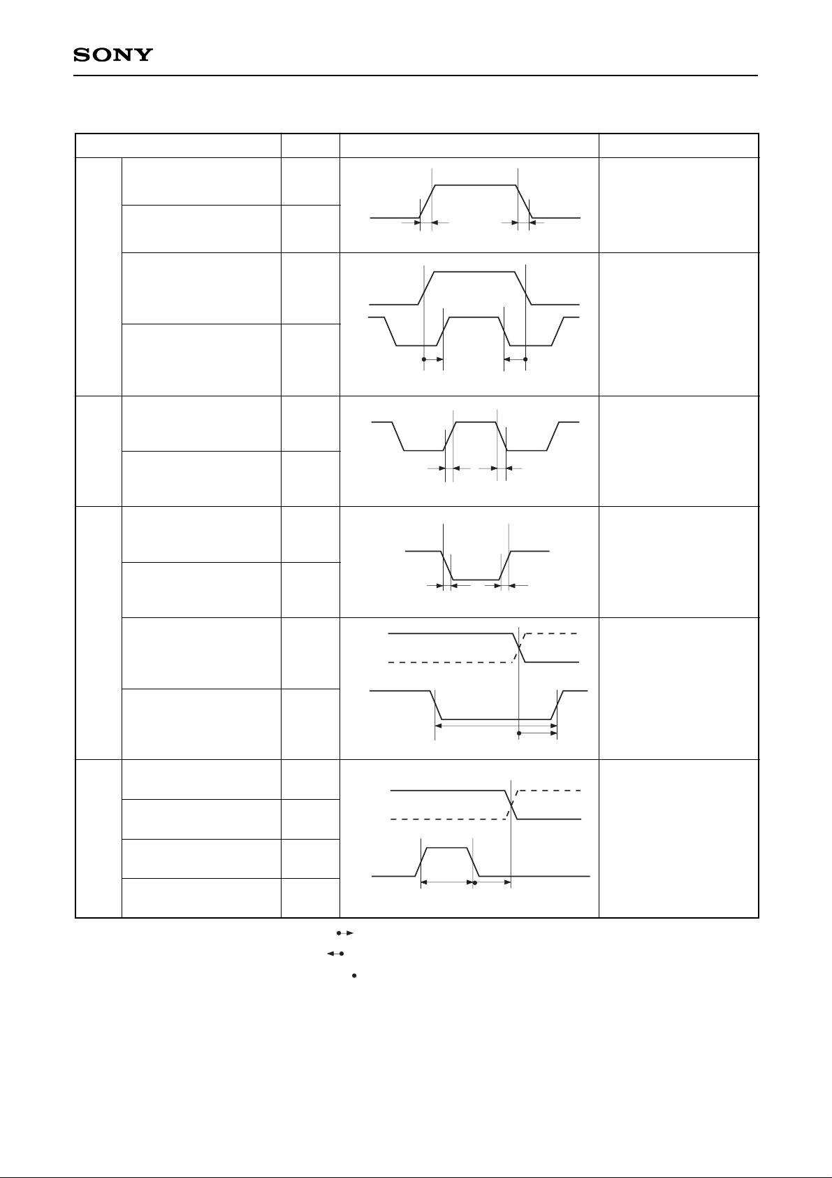
<Vertical Shift Register Driving Waveform>
Vst rise time
VST
VCK
ENB
PCG
Vst fall time
Vst data set-up time
Vst data hold time
Vck rise time
Vck fall time
Enb rise time
Enb fall time
Vck rise/fall to Enb rise
time
Enb pulse width
trVst
tfVst
tdVst
thVst
trVck
tfVck
trEnb
tfEnb
tdEnb
twEnb
Pcg rise time trPcg
Pcg fall time tfPcg
Pcg fall to Vck rise/fall
time
toVck
Pcg pulse width twPcg
∗5
Definitions: The right-pointing arrow ( ) means +.
The left-pointing arrow ( ) means –.
The black dot at an arrow ( ) indicates the start of measurement.
90%
10%
10%
90%
Vst
trVst tfVst
50%
50%
∗
5
Vst
Vck
tdVst thVst
50%
50%
Vck
10%
10%
90%
90%
trVckn tfVckn
90%
90%
10%
10%
tfEn trEn
Enb
Enb
50%
50%
50%
twEnb
tdEnb
Vck
∗
5
Pcg
50%
50%
50%
twPcg toVck
Vck
∗
5
Item Symbol Waveform Conditions
Page 9
– 9 –
LCX019AM
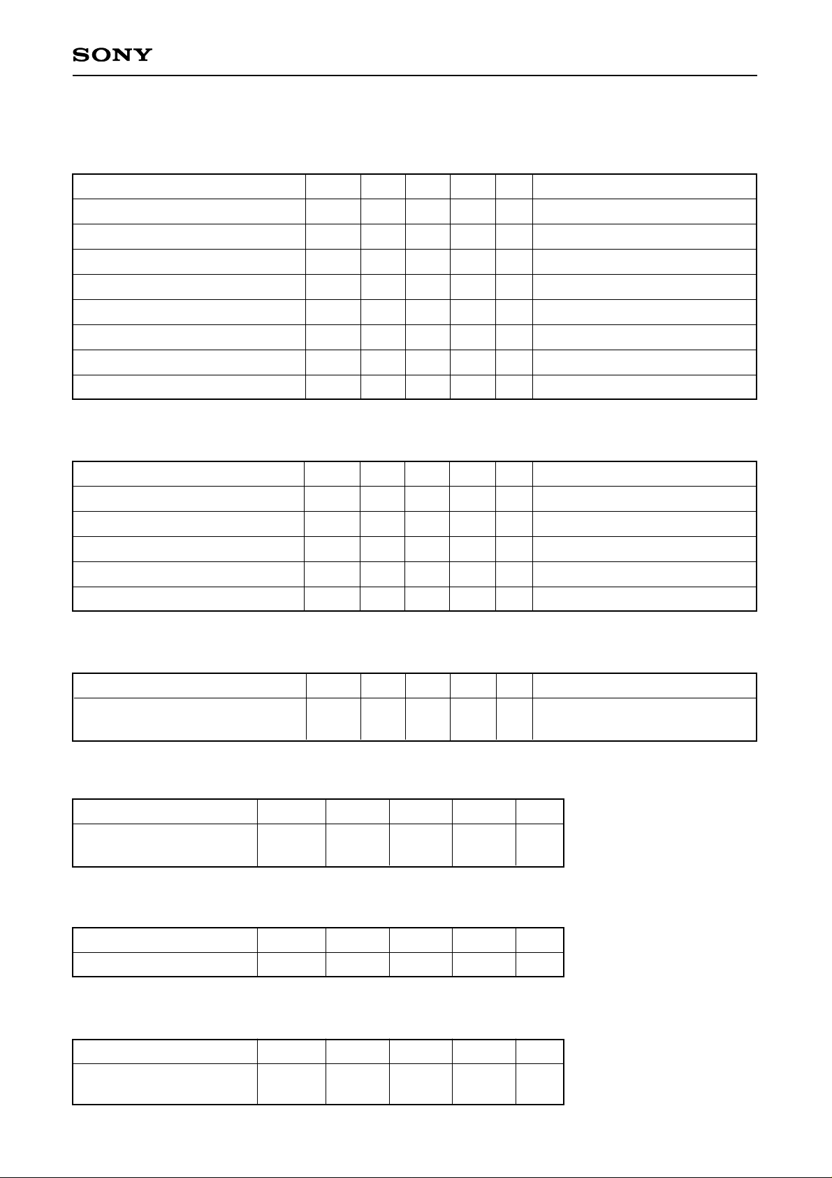
Electrical Characteristics (Ta = 25°C, HVDD = 13.5V, VVDD = 13.5V, AVDD =15.5V)
1. Horizontal drivers
Item
Input pin capacitance HCKn
HST
Input pin current HCK1
HCK2
HST
RGT
Video signal input pin capacitance
Current consumption
CHckn
CHst
Csig
IH
HCK1 = GND
HCK2 = GND
HST = GND
RGT = GND
HCKn: HCK1, HCK2 (3.82MHz)
—
—
–500
–1000
–500
–150
—
—
12
12
–100
–350
–150
–30
250
3.5
17
17
—
—
—
—
—
7
pF
pF
µA
µA
µA
µA
pF
mA
Symbol Min. Typ. Max. Unit Conditions
2. Vertical drivers
Input pin capacitance VCK
VST
Input pin current VCK
PCG, VST, ENB, DWN
Current consumption
CVck
CVst
IV
—
—
–500
–150
—
12
12
–150
–30
1.1
17
17
—
—
4
pF
pF
µA
µA
mA
4. Total power consumption of the panel
Item
Total power consumption
of the panel (NTSC)
PWR — 80 160 mW
Symbol Min. Typ. Max. Unit
5. Pin input resistance
Item
Pin – VSS input resistance Rpin 0.4 1 — MΩ
Symbol Min. Typ. Max. Unit
VCK = GND
PCG, VST, EN, DWN = GND
VCK: (15.7kHz)
3. Analog block
Current consumption IA — 1.4 4 mA
HCKn, HCK1, HCK2 (3.82MHz)
VCK (15.7kHz)
6. Uniformity improvement signal input capacitance
Item
Uniformity improvement
signal
CPSIGon 13
—
16
nF
Symbol Min. Typ. Max. Unit
Item Symbol Min. Typ. Max. Unit Conditions
Item Symbol Min. Typ. Max. Unit Conditions
Page 10
– 10 –
LCX019AM
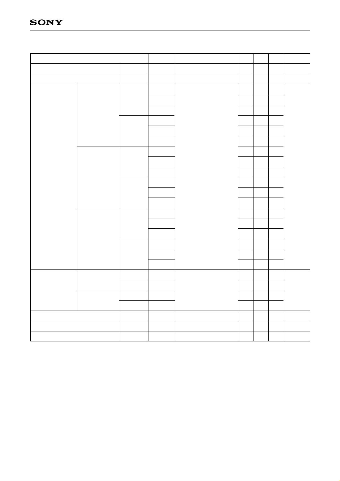
Electro-optical Characteristics (Ta = 25°C, NTSC mode)
Item
Contrast ratio
60°C
60°C
25°C
60°C
25°C
60°C
25°C
60°C
0°C
25°C
0°C
25°C
60°C
25°C
25°C
CR60
Teff
RV90-25
GV90-25
BV90-25
RV90-60
GV90-60
BV90-60
RV50-25
GV50-25
BV50-25
RV50-60
GV50-60
BV50-60
RV10-25
GV10-25
BV10-25
RV10-60
GV10-60
BV10-60
ton0
ton25
toff0
toff25
F
YT60
CTK
130
60
1.0
1.0
1.1
1.0
1.0
1.1
1.4
1.5
1.6
1.4
1.4
1.5
1.7
1.7
1.8
1.7
1.8
1.8
—
—
—
—
—
—
—
200
70
1.3
1.4
1.6
1.3
1.4
1.6
1.7
1.8
1.9
1.7
1.8
1.9
2.1
2.2
2.3
2.1
2.2
2.3
30
17
100
30
–65
—
—
—
—
1.7
1.8
1.9
1.7
1.8
1.9
2.0
2.1
2.2
2.1
2.1
2.2
2.6
2.6
2.7
2.6
2.7
2.7
80
40
200
70
–40
0
5
1
2
3
4
5
6
7
—
%
V
ms
dB
s
%
Effective aperture ratio
V90
V50
V10
ON time
OFF time
V-T
characteristics
Response time
Flicker
Image retention time
Cross talk
Symbol Measurement method Min. Typ. Max. Unit
Page 11
– 11 –
LCX019AM
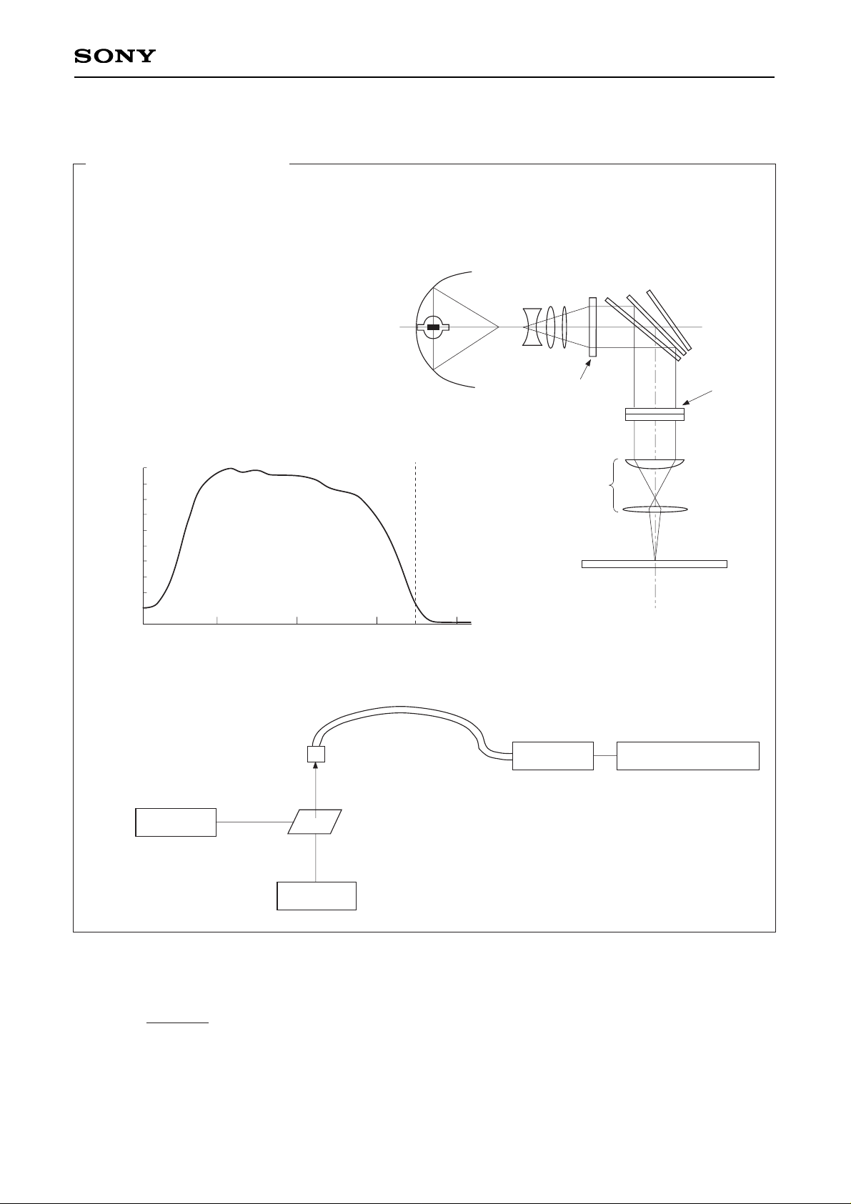
<Electro-optical Characteristics Measurement>
• Measurement system II
LIght Detector
Measurement Equipment
Optical fiber
LCD panel
Light receptor lens
Drive Circuit
Light Source
Basic measurement conditions
(1) Driving voltage
HVDD = 13.5V, VVDD = 13.5V, AVDD = 15.5V
VVC = 7.0V, Vcom = 6.8V
(2) Measurement temperature
25°C unless otherwise specified.
(3) Measurement point
One point in the center of screen unless
otherwise specified.
(4) Measurement systems
Two types of measurement system are used
as shown below.
(5) Video input signal voltage (Vsig)
Vsig = 7.0 ± VAC [V] (VAC: signal amplitude)
(6) Optical measurement systems
Elliptic mirror
Relay lens system
B
R
G
Dichroic
mirrors
Fresnel lens
LCD panel
Projection lenses
Screen
100W lamp angle distribution
Panel incident light dispersion angle [ ° ]
Relative light intensity
0.0 1.0 2.0 3.0 3.5 4.0
1
0.9
0.8
0.7
0.6
0.5
0.4
0.3
0.2
0.1
0
• Measurement system I
1. Contrast ratio
Contrast Ratio (CR) is given by the following formula (1).
L (White)
CR =
L (Black) ...... (1)
L (White): Surface luminance of the TFT-LCD panel at the input signal amplitude VAC = 0.5V
L (Black): Surface luminance of the panel at VAC = 4.5V
Both luminosities are measured by System I.
Page 12
– 12 –
LCX019AM
2. Effective aperture ratio
Measure the luminances below on the screen in System I, and calculate the effective aperture ratio using
the following formula (2).
Luminance for panel with microlens
× (TFT aperture ratio) × 100 [%] ...... (2)
Luminance for panel without microlens
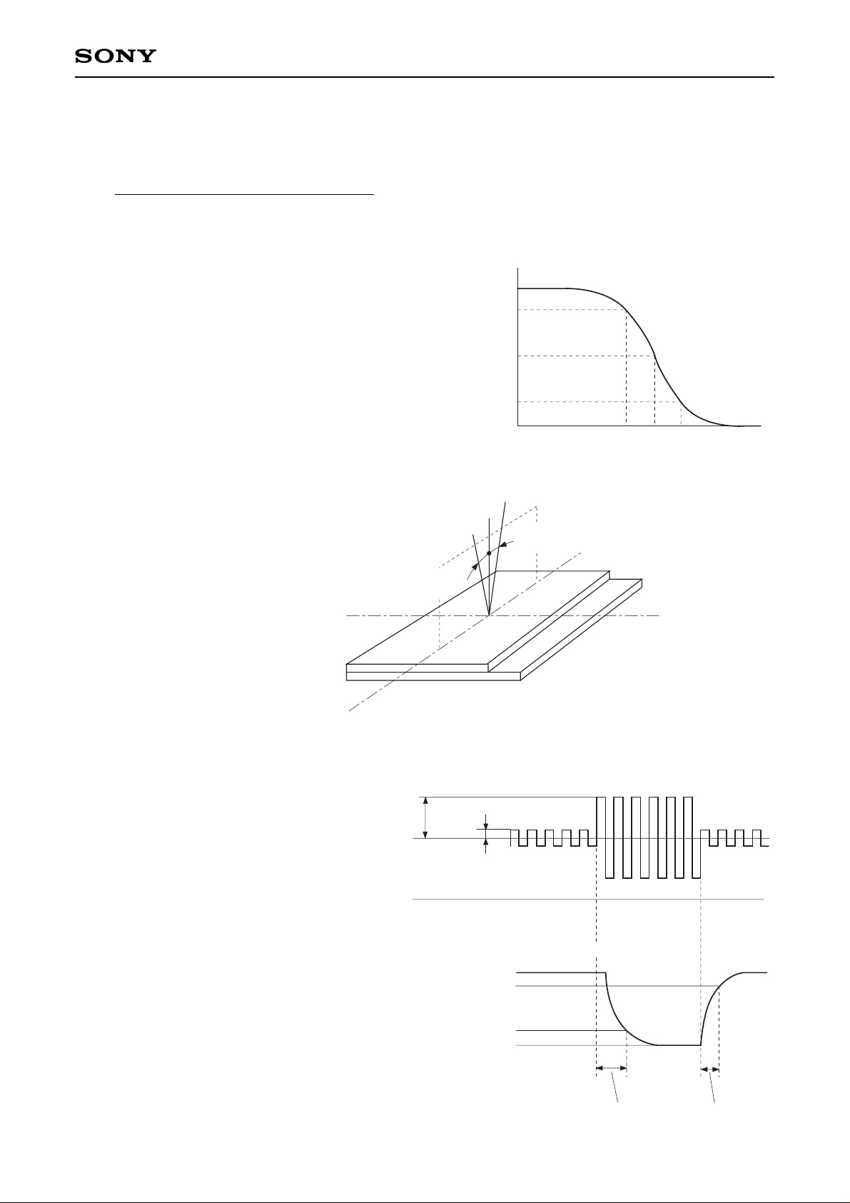
3. V-T characteristics
V-T characteristics, the relationship between signal
amplitude and the transmittance of the panels, are
measured by System II. V90, V50 and V10 correspond
to the each voltage which defines 90%, 50% and 10%
of transmittance respectively.
The angles of incidence for R, G and B are as shown
in the diagram below.
Red: Center: Vertical
Green: Left: 7.75 ± 0.5°
Blue: Right: 7.75 ± 0.5°
4. Response time
Response time ton and toff are defined by
the formulas (3) and (4) respectively.
ton = t1 – tON ...... (3)
toff = t2 – tOFF ...... (4)
t1: time which gives 10% transmittance of
the panel.
t2: time which gives 90% transmittance of
the panel.
The relationships between t1, t2, tON and
tOFF are shown in the right figure.
90
50
10
V
90 V50 V10
VAC – Signal amplitude [V]
Transmittance [%]
Input signal voltage (waveform applied to the measured pixels)
4.5V
0.5V
7.0V
0V
Optical transmission output waveform
100%
90%
10%
0%
tON t1
ton
tOFF t2
toff
Center
Right
Left
Pad
Optimum angle of
incidence 7.75 ± 0.5°
Optimum angle of
incidence 7.75 ± 0.5°
Page 13
– 13 –
LCX019AM
5. Flicker
Flicker (F) is given by the formula (5). DC and AC (NTSC: 30Hz, rms, PAL: 25Hz, rms) components of the
panel output signal for gray raster∗mode are measured by a DC voltmeter and a spectrum analyzer in
system II.
AC component
F [dB] = 20log
{ }
...... (5)
DC component
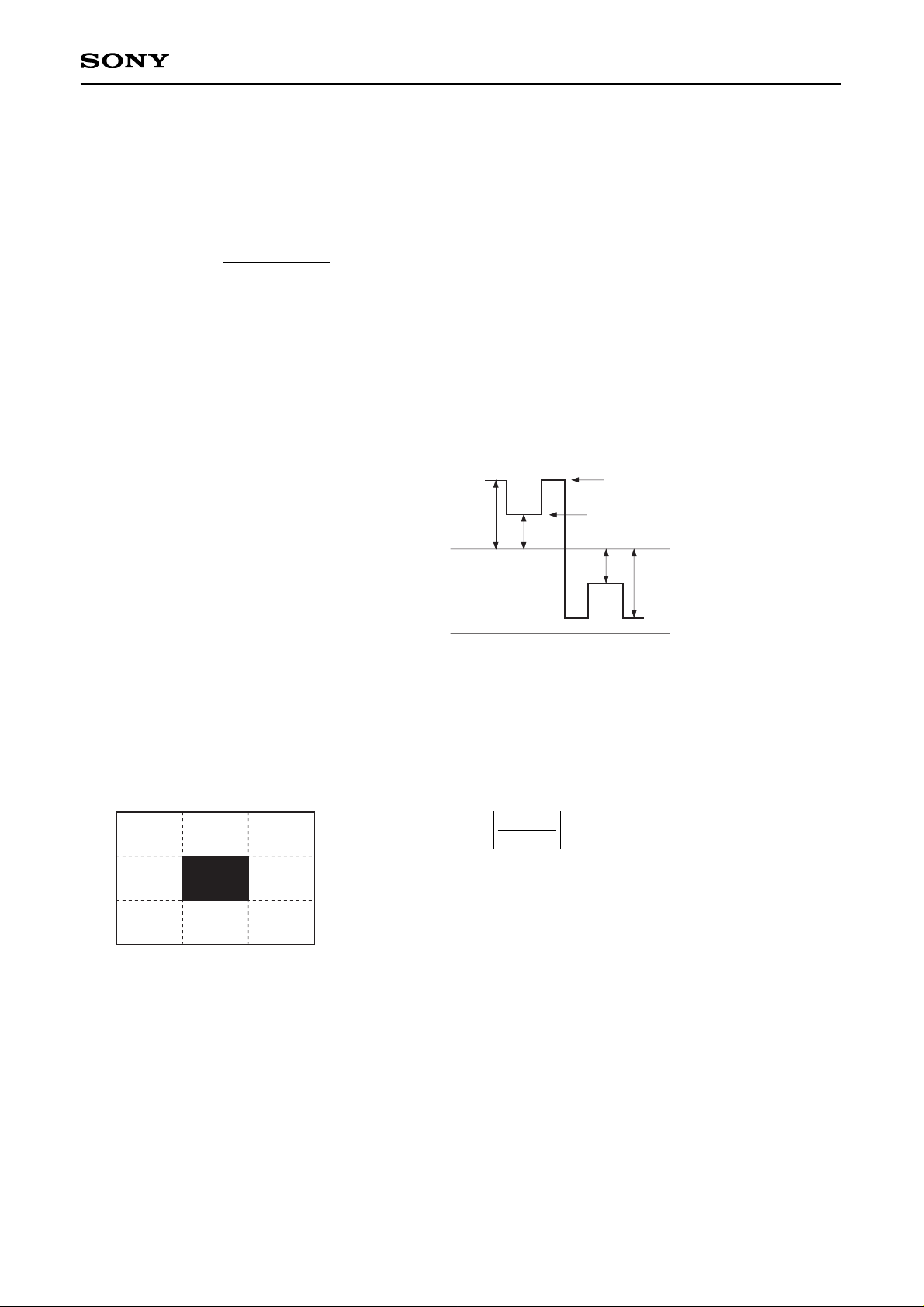
6. Image retention time
Image retention time is given by following procedures.
Apply the monoscope signal to the LCD panel for 60 minutes and then change this signal to the gray scale
of Vsig = 7.0 ± VAC (VAC: 3 to 4V). Hold VAC that maximizes image retention judging by sight. Measure the
time till the residual image becomes indistinct.
∗
Monoscope signal conditions:
Vsig = 7.0 ± 4.5 or ±2.0 [V]
(shown in the right figure)
Vcom = 6.8V
7. Cross talk
Cross talk is determined by the luminance differences between adjacent areas represented Wi' and Wi (i =
1 to 4) around black window (Vsig = 4.5V/1V).
Cross talk CTK = × 100 [%]
∗
Each input signal condition for gray raster mode is given by
Vsig = 7.0 ± V50 [V]
where: V50 is the signal amplitude which gives 50% of
transmittance in V-T characteristics.
Black level
White level
Vsig waveform
7.0V
0V
4.5V
2.0V
4.5V
2.0V
W1 W1'
W3 W3'
W2
W2'
W4
W4'
Wi' – Wi
Wi
Page 14
– 14 –
LCX019AM
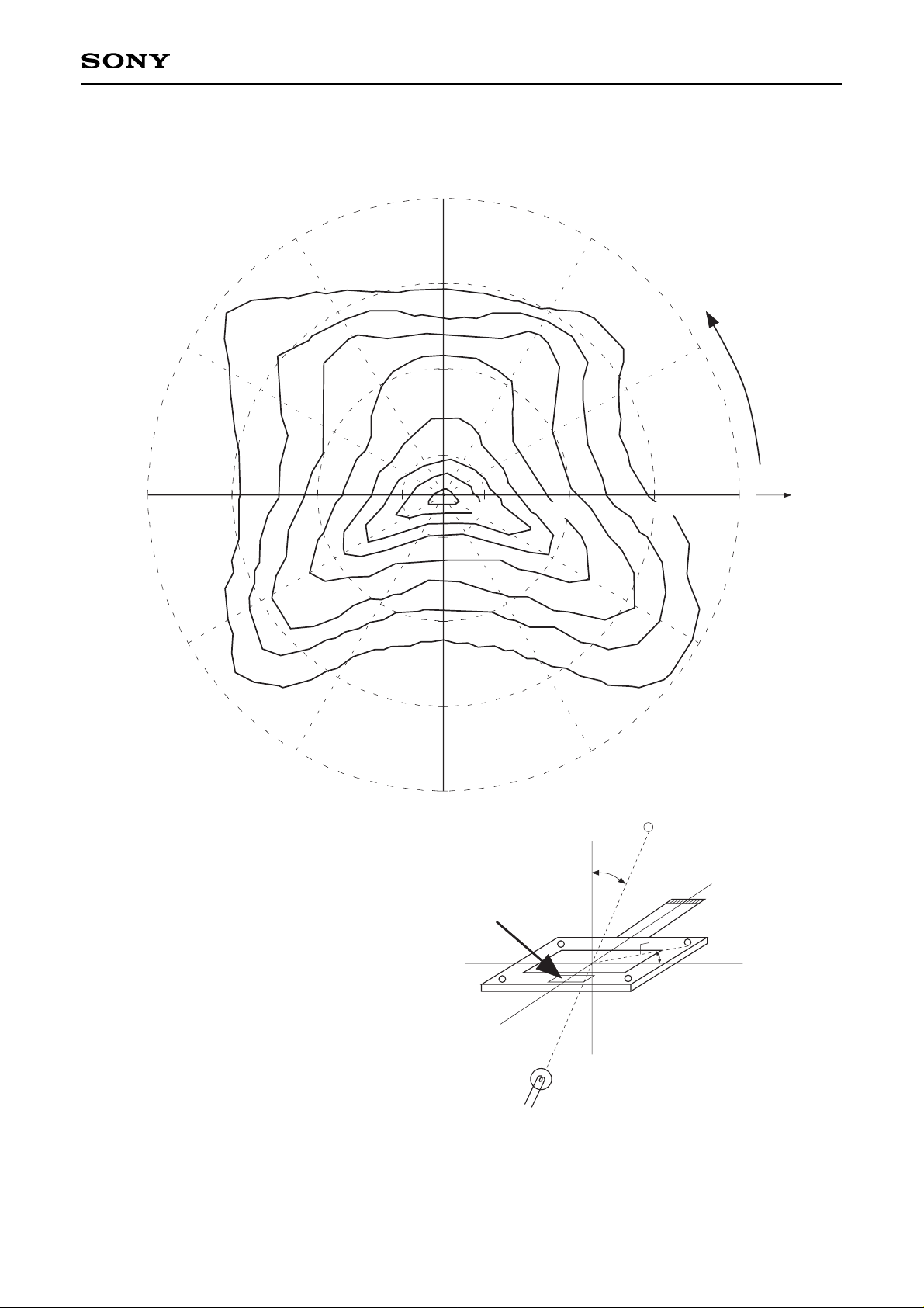
Viewing Angle Characteristics (Typical Value)
90
270
180
0
Theta
Phi
70
θ
φ
φ180°
X
φ270°
Y
φ0°
φ90°
Z
θ0°
Marking
Measurement method
30 5010
Note) This measurement is performed using an LCD panel without a microlens.
Page 15
– 15 –
LCX019AM
Description of Operation
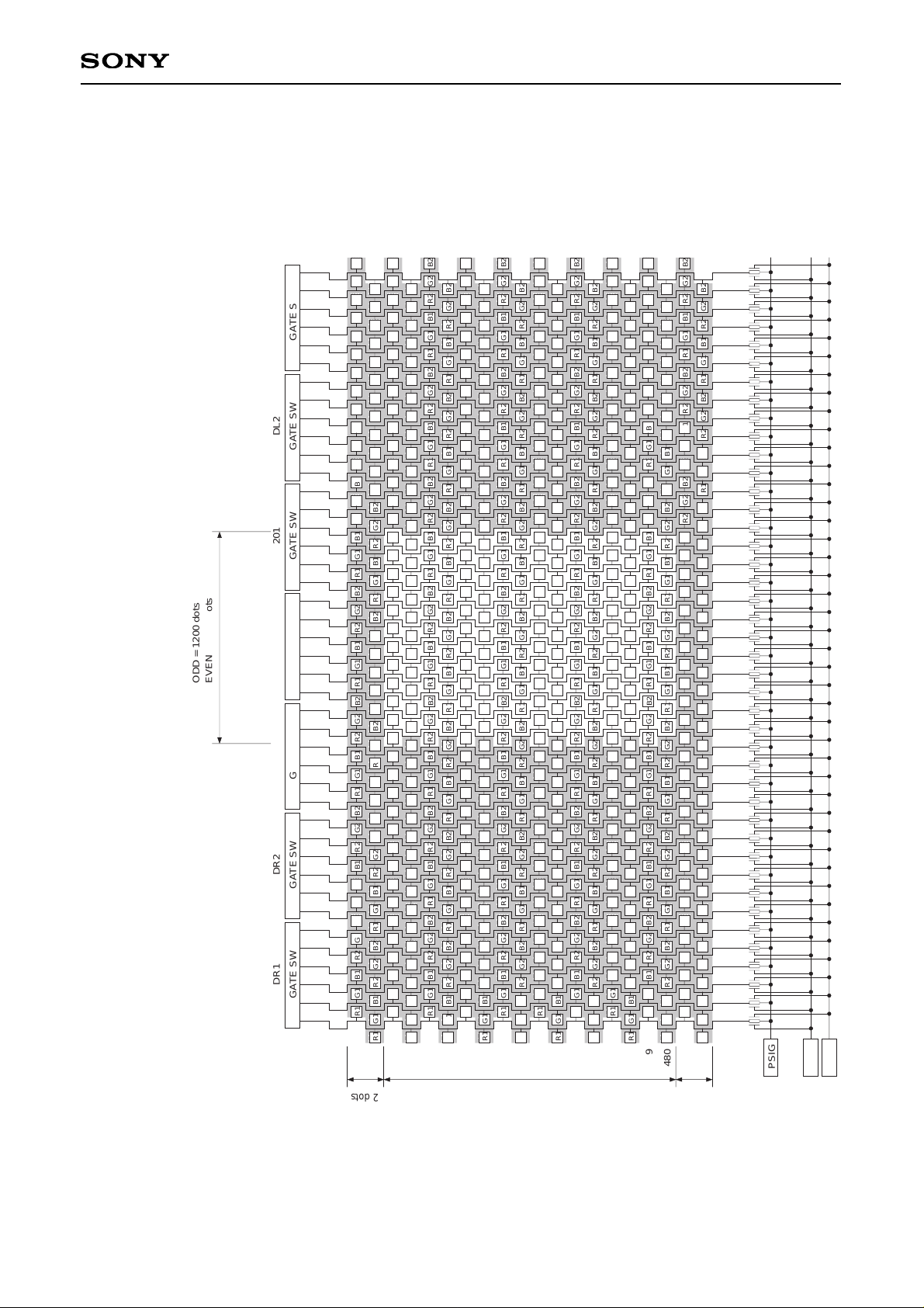
1 Dot arrangement (1)
The dots are arranged in a delta pattern. The shaded area is used for the dark border around the display.
PC
PCX
GATE SW
DR1
PSIG
GATE SW
DR2
GATE SW
1
GATE SW
GATE SW
201
GATE SW
DL2
GATE SW
DR1
1
2
3
4
479
480
ODD = 1200 dots
EVEN = 1199 dots
R1
2 dots
G1 B1
R1 G1 B1 R2 G2 B2 R1 G1 B1 R2 G2 B2
R2 G2 B2 R1 G1 B1 R2 G2 B2 R1 G1 B1 G2 B2
R2 G2
B2
R1 G1 B1 R2 G2 B2 R1 G1 B1
R1 G1 B1 R2 G2 B2 R1 G1 B1 R2 G2 B2
R1 G1 B1
R2 G1 B1
R1 G1 B1 R2 G2 B2 R1 G1 B1 R2 G2 B2
R2 G2 B2 R1 G1 B1 R2 G2 B2
R2 G2 B2
R1
480 dots
2 dots
R1 G1 B1
R1 G1 B1 R2 G2 B2 R1 G1 B1 R2 G2 B2
R2 G2 B2 R1 G1 B1 R2 G2 B2 R1 G1 B1 G2 B2
R2 G2
B2
R1 G1 B1 R2 G2 B2 R1 G1 B1
R1 G1 B1 R2 G2 B2 R1 G1 B1 R2 G2 B2
R1 G1 B1
R2 G1 B1
R1 G1 B1 R2 G2 B2 R1 G1 B1 R2 G2 B2
R2 G2 B2 R1 G1 B1 R2 G2 B2
R2 G2 B2
R1
R1 G1 B1
R1 G1 B1 R2 G2 B2 R1 G1 B1 R2 G2 B2
R2 G2 B2 R1 G1 B1 R2 G2 B2 R1 G1 B1 G2 B2
R2 G2
B2
R1 G1 B1 R2 G2 B2 R1 G1 B1
R1 G1 B1 R2 G2 B2 R1 G1 B1 R2 G2 B2
R1 G1 B1
R2 G1 B1
R1 G1 B1 R2 G2 B2 R1 G1 B1 R2 G2 B2
R2 G2 B2 R1 G1 B1 R2 G2 B2
R2 G2 B2
R1
R1 G1 B1
R1 G1 B1 R2 G2 B2 R1 G1 B1 R2 G2 B2
R2 G2 B2 R1 G1 B1 R2 G2 B2 R1 G1 B1 G2 B2
R2 G2
B2
R1 G1 B1 R2 G2 B2 R1 G1 B1
R1 G1 B1 R2 G2 B2 R1 G1 B1 R2 G2 B2
R1 G1 B1
R2 G1 B1
R1 G1 B1 R2 G2 B2 R1 G1 B1 R2 G2 B2
R2 G2 B2 R1 G1 B1 R2 G2 B2
R2 G2 B2
R1
R1 G1 B1
R1 G1 B1 R2 G2 B2 R1 G1 B1 R2 G2 B2
R2 G2 B2 R1 G1 B1 R2 G2 B2 R1 G1 B1 G2 B2
R2 G2
B2
R1 G1 B1 R2 G2 B2 R1 G1 B1
R1 G1 B1 R2 G2 B2 R1 G1 B1 R2 G2 B2
R1 G1 B1
R2 G1 B1
R1 G1 B1 R2 G2 B2 R1 G1 B1 R2 G2 B2
R2 G2 B2 R1 G1 B1 R2 G2 B2
R2 G2 B2
R1
R1 G1 B1
R1 G1 B1 R2 G2 B2 R1 G1 B1 R2 G2 B2
R2 G2 B2 R1 G1 B1 R2 G2 B2 R1 G1 B1 G2 B2
R2 G2
B2
R1 G1 B1 R2 G2 B2 R1 G1 B1
R1 G1 B1 R2 G2 B2 R1 G1 B1 R2 G2 B2
R1 G1 B1
R2 G1 B1
R1 G1 B1 R2 G2 B2 R1 G1 B1 R2 G2 B2
R2 G2 B2 R1 G1 B1 R2 G2 B2
R2 G2 B2
R1
R1 G1 B1
R1 G1 B1 R2 G2 B2 R1 G1 B1 R2 G2 B2
R2 G2 B2 R1 G1 B1 R2 G2 B2 R1 G1 B1 G2 B2
R2 G2
B2
R1 G1 B1 R2 G2 B2 R1 G1 B1
R1 G1 B1 R2 G2 B2 R1 G1 B1 R2 G2 B2
R1 G1 B1
R2 G1 B1
R1 G1 B1 R2 G2 B2 R1 G1 B1 R2 G2 B2
R2 G2 B2 R1 G1 B1 R2 G2 B2
R2 G2 B2
R1
R1 G1 B1
R1 G1 B1 R2 G2 B2 R1 G1 B1 R2 G2 B2
R2 G2 B2 R1 G1 B1 R2 G2 B2 R1 G1 B1 G2 B2
R2 G2
B2
R1 G1 B1 R2 G2 B2 R1 G1 B1
R1 G1 B1 R2 G2 B2 R1 G1 B1 R2 G2 B2
R1 G1 B1
R2 G1 B1
R1 G1 B1 R2 G2 B2 R1 G1 B1 R2 G2 B2
R2 G2 B2 R1 G1 B1 R2 G2 B2
R2 G2 B2
R1
R1 G1 B1
R1 G1 B1 R2 G2 B2 R1 G1 B1 R2 G2 B2
R2 G2 B2 R1 G1 B1 R2 G2 B2 R1 G1 B1 G2 B2
R2 G2
B2
R1 G1 B1 R2 G2 B2 R1 G1 B1
R1 G1 B1 R2 G2 B2 R1 G1 B1 R2 G2 B2
R1 G1 B1
R2 G1 B1
R1 G1 B1 R2 G2 B2 R1 G1 B1 R2 G2 B2
R2 G2 B2 R1 G1 B1 R2 G2 B2
R2 G2 B2
R1
R1 G1 B1
R1 G1 B1 R2 G2 B2 R1 G1 B1 R2 G2 B2
R2 G2 B2 R1 G1 B1 R2 G2 B2 R1 G1 B1 G2 B2
R2 G2
B2
R1 G1 B1 R2 G2 B2 R1 G1 B1
R1 G1 B1 R2 G2 B2 R1 G1 B1 R2 G2 B2
R1 G1 B1
R2 G1 B1
R1 G1 B1 R2 G2 B2 R1 G1 B1 R2 G2 B2
R2 G2 B2 R1 G1 B1 R2 G2 B2
R2 G2 B2
R1
Page 16
– 16 –
LCX019AM
2. LCD panel operations
[Description of basic operations]
The basic operations of the LCD panel are shown below based on the wide-display mode.
• A vertical driver, which consists of vertical shift registers, enable-gates and buffers, applies a selected pulse
to every 480 gate lines sequentially in every horizontal scanning period.
• A horizontal driver, which consists of horizontal shift registers, gates and CMOS sample-and-hold circuits,
applies selected pulses to every 1199.5 signal electrodes sequentially in a single horizontal scanning period.
• Vertical and horizontal shift registers address one pixel, and then turn on Thin Film Transistors (TFTs; two
TFTs) to apply a video signal to the dot. The same procedures lead to the entire 480 × 1199.5 dots to display
a picture in a single vertical scanning period.
• The LCD pixel dots are arranged in a delta pattern, where the dots connected to the identical signal line is
positioned with 1.5-dot offset against an adjacent horizontal line. Horizontal Start Pulse (HST) is generated
with 1.5-bit offset between the horizontal lines to regulate the above offset. HCK and sample-and-hold (S/H)
pulses follow the same 1.5-bit offset scheme.
• The video signal shall be input with polarity-inverted system in every horizontal cycle.
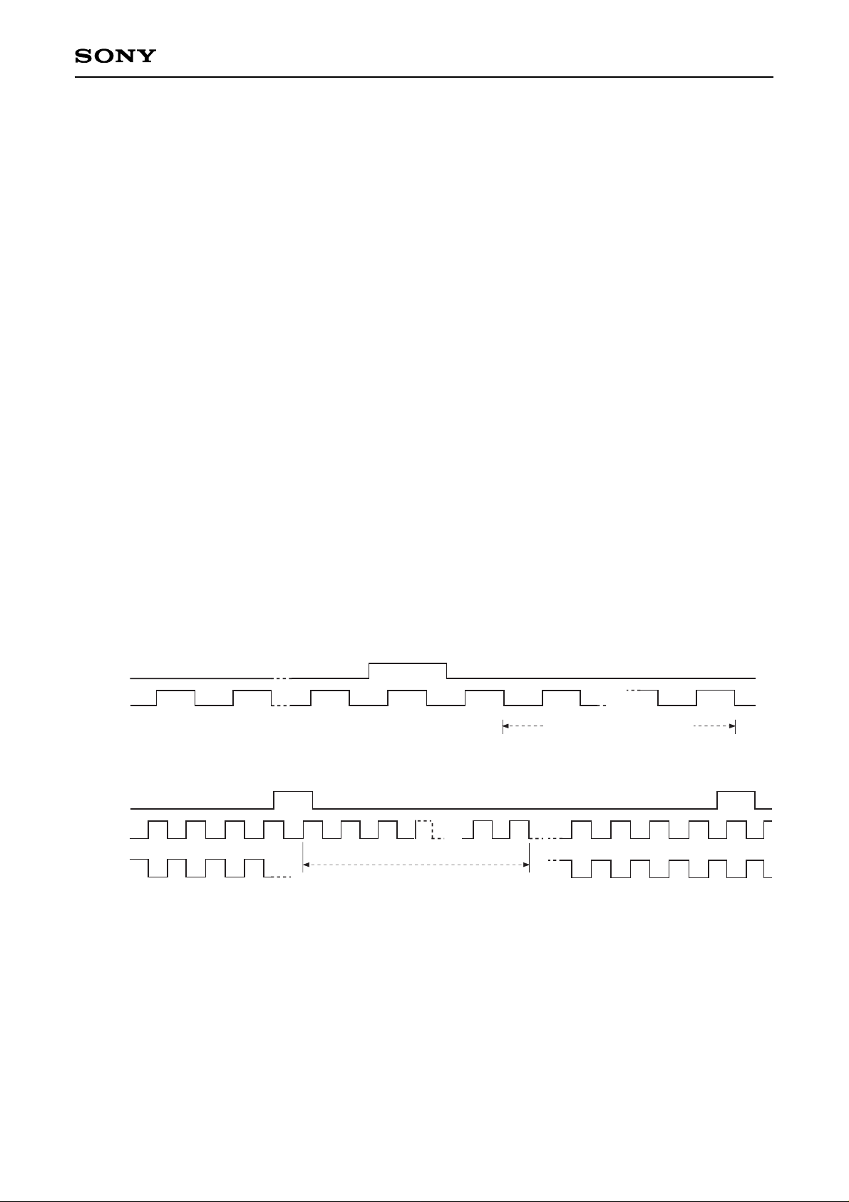
• Timing diagrams of the vertical and the horizontal display cycle are shown below:
Vertical display cycle 480H
1 2 480
(1) Vertical display cycle
VST
VCK
(2) Horizontal display cycle
Horizontal display cycle
1 2 3 4 5 6
200
201
HST
HCK1
HCK2
Page 17
– 17 –
LCX019AM
[Description of operating mode]
The LCD panel has the following functions to easily apply to various uses, as well as various broadcasting
systems.
• Right/left inverse mode
• Up/down inverse mode
These modes are controlled by two signals (RGT and DWN). The setting mode is shown below:
DWN
HLDown scan
Up scan
ModeRGT
H
L
Right scan
Left scan
Mode
S/H
CK1
CK2
SIG3
SIG6
SIG2
LCX019AM
SIG3
SIG6
SIG2
SIG1
SIG1
SIG5
SIG5
SIG4
SIG4
CK3
CK4
CK5
S/H
S/H
S/H
S/H
S/H
CK6
S/H
S/H
S/H
S/H
S/H
4
5
6
7
8
9
The direction of the right/left and/or up/down mean when Pin 1 marking is located at right side with the pin
block upside.
• The analog signal (PSIG) shall be input by 1H inversion synchronized with the video signal.
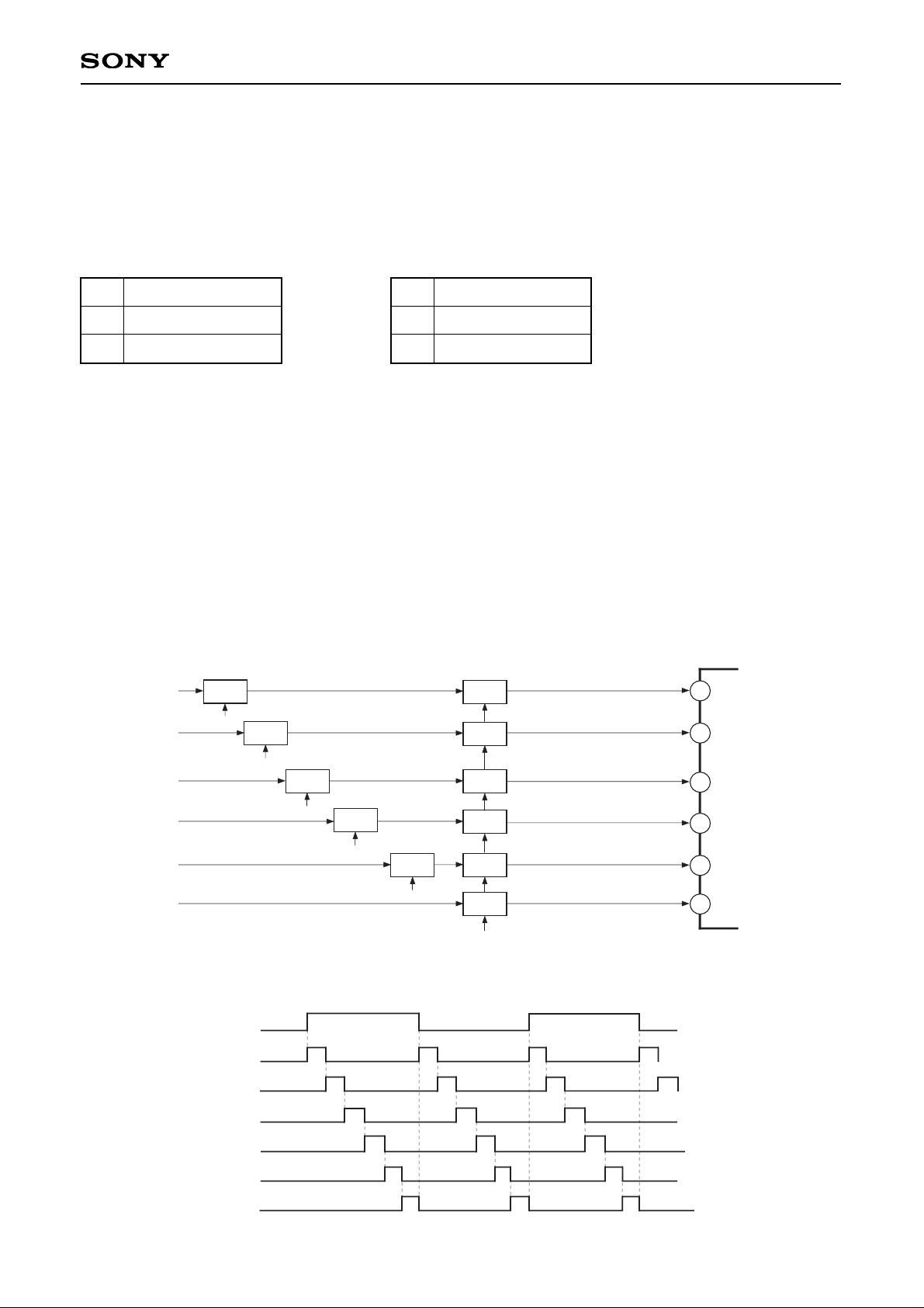
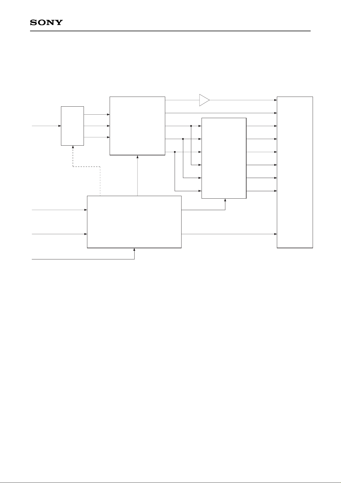
3. 6-dot simultaneous sampling
Horizontal driver samples SIG1 to SIG6 signals simultaneously, which requires the phase matching between
signals to prevent horizontal resolution from deteriorating. Thus phase matching between each signal is
required using an external signal delaying circuit before applying video signal to the LCD panel.
The block diagram of the delaying procedure using simple-and-hold method is as follows.
The LCX019AM has the right/left inverse function. The following phase relationship diagram indicates the
phase setting for the right scan (RGT = High level). For the left scan (RGT = Low level), the phase setting shall
be inverted in the order of the SIG6, SIG4, SIG5, SIG3, SIG1 and SIG2 signals.
HCKn
CK1
CK3
CK5
CK2
CK4
CK6
<Phase relationship of delaying sample-and-hold pulses> (right scan)
Page 18
– 18 –
LCX019AM
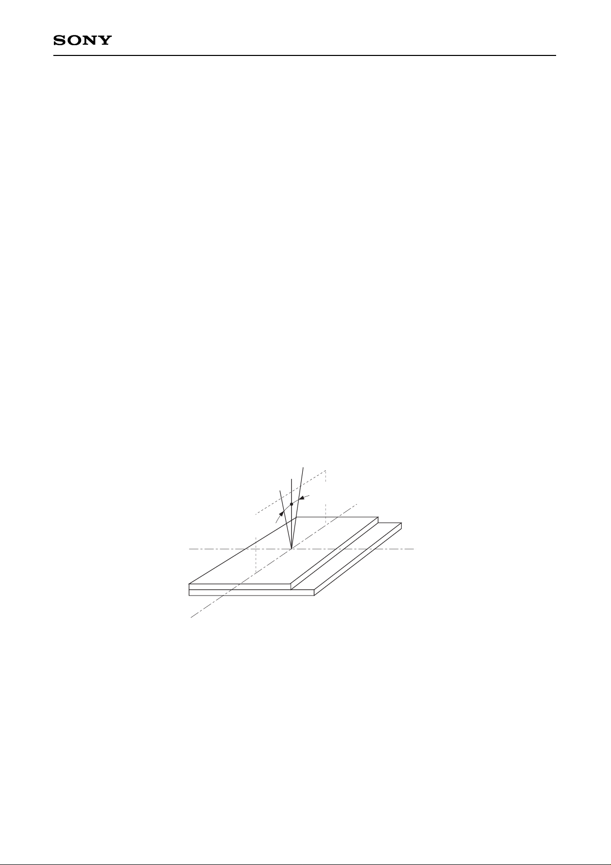
Display System Block Diagram
An example of display system is shown below.
RGB Driver
CXA1853AQ
Double
speed R
Double
Speed
System
COM
SIG2 (R1)
SIG1 (G1)
SIG3 (B1)
SIG5 (R2)
SIG4 (G2)
SIG6 (B2)
B
G
R
Sample-and-Hold IC
CXA2504N
FRP
Timing Generator
CXD2443Q
NTSC, PAL
VD
HD or double speed HD
Serial control
S/H1 to 7
HCK1&2, VCK, ENB, VST,
PCG1, HST, RGT, DWN
LCD Panel
LCX019AM
PSIG
Buffer
SID
Double
speed G
Double
speed B
Page 19
– 19 –
LCX019AM
Optical Characteristics
1. Microlens outline
The LCX019AM has a single built-in microlens on the substrate side facing the TFT for the three TFT panel
picture elements. This microlens serves the following purposes.
(1) The microlens converges the incident light striking the LCD panel to the dot aperture in order to improve
the effective aperture ratio and increase the display brightness.
(2) The microlens provides a color representation by distributing the light flux for each of the three primary
colors R, G and B which strike the panel at different angles to the dot apertures corresponding to each
color.
This allows the light utilization efficiency to be improved by eliminating the light absorption by the color filter,
which had been unavoidable with conventional single panel projectors.
2. Recommended lighting conditions
In order to bring out the full light converging effects of the microlens and provide a color representation with
high color purity, the following lighting is recommended.
(1) The incident light angle of the three primary colors should be as shown in the figure below. The center light
should strike the panel from the panel normal direction, and the left and right light from angles inclined to the
right and left of the panel normal direction. The design optimal angle of incidence is the range of 7.75 ± 0.5°.
However, the optimal angle of incidence may be altered slightly depending on the panel. Be sure to allow
adjustment of the mutual angles of the dichroic mirrors so that the angle of incidence can be varied within the
range of 7.75 ± 0.5°.
Center
Right
Left
Pad
Optimum angle of
incidence 7.75 ± 0.5°
Optimum angle of
incidence 7.75 ± 0.5°
(2) Effective light: The normal direction (center light), left light and right light noted above should strike the
panel at an angle of ±3.5° or less. Light with a dispersion angle greater than this value will
strike adjoining dot apertures and cause the color purity to worsen. (See the incident angle
distribution for System I.)
3. Recommended projection optical system
The maximum egress light angle for light passing through the LCD is approximately ±20°. Therefore, setting
the F stop of the projection lens to about 1.5 is recommended in order to maximize the light converging effects
of the microlens and provide a representation with excellent color balance. If the projection lens F stop is larger
than this value, the right and left light are kicked accordingly by the projection lens, thereby reducing the
egress light flux to the screen and the same time shifting the white balance.
Page 20

– 20 –
LCX019AM
Notes on Operation
(1) Lighting spectrum and intensity
Use only visible light with a wavelength λ = 415 to 780nm as a light source. Light with a wavelength λ > 780nm
(infrared light) will produce unwanted temperature rises. Light with a wavelength λ < 415nm (ultraviolet
light) will produce irreversible changes in the display characteristics. To prevent this, be sure to mount
UV/IR cut filters between the LCX019AM and the light source as necessary depending on the light source.
The lighting intensity should be 1 million lux or less, and the panel surface temperature should not exceed
55°C.
(2) Lighting optical system
Care should be taken for the following points concerning the optical system mounted on the LCX019AM.
1) Light reflected from the optical system to the panel should be 20,000 lux or less.
2) Particular care should be taken for the panel incident angle distribution when designing optical systems
for use with the LCX019AM.
3) The panel surface temperature distribution should not exceed 10°C.
4) Light should shine only on the effective display area within the LCD panel and not on other unnecessary
locations. Leakage light may produce unwanted temperature rises.
Page 21

– 21 –
LCX019AM
Notes on Handling
(1) Static charge prevention
Be sure to take following protective measures. TFT-LCD panels are easily damaged by static charge.
a) Use non-chargeable gloves, or simply use bare hands.
b) Use an earth-band when handling.
c) Do not touch any electrodes of a panel.
d) Wear non-chargeable clothes and conductive shoes.
e) Install conductive mat on the working floor and working table.
f) Keep panels away from any charged materials.
g) Use ionized air to discharge the panels.
(2) Protection from dust and dirt
a) Operate in clean environment.
b) When delivered, a surface of a panel (glass panel) is covered by a protective sheet.
Peel off the protective sheet carefully not to damage the glass panel.
c) Do not touch the surface of the glass panel. The surface is easily scratched. When cleaning, use a
clean-room wiper with isopropyl alcohol. Be careful not to leave stain on the surface.
d) Use ionized air to blow off dust at the glass panel.
(3) Other handling precautions
a) Do not twist or bend the flexible PC board especially at the connecting region because the board is
easily deformed.
b) Do not drop a panel.
c) Do not twist or bend a panel or panel frame.
d) Keep a panel away from heat source.
e) Do not dampen a panel with water or other solvents.
f) Avoid to store or to use a panel in a high temperature or in a high humidity, which may result in panel
damages.
g) Minimum radius of bending curvature for a flexible substrate must be 1mm.
h) Torque required to tighten screws on a panel must be 3kg · cm or less.
i) Use appropriate filter to protect a panel.
j) Do not pressure the portion other than mounting hole (cover).
Page 22
– 22 –
LCX019AM
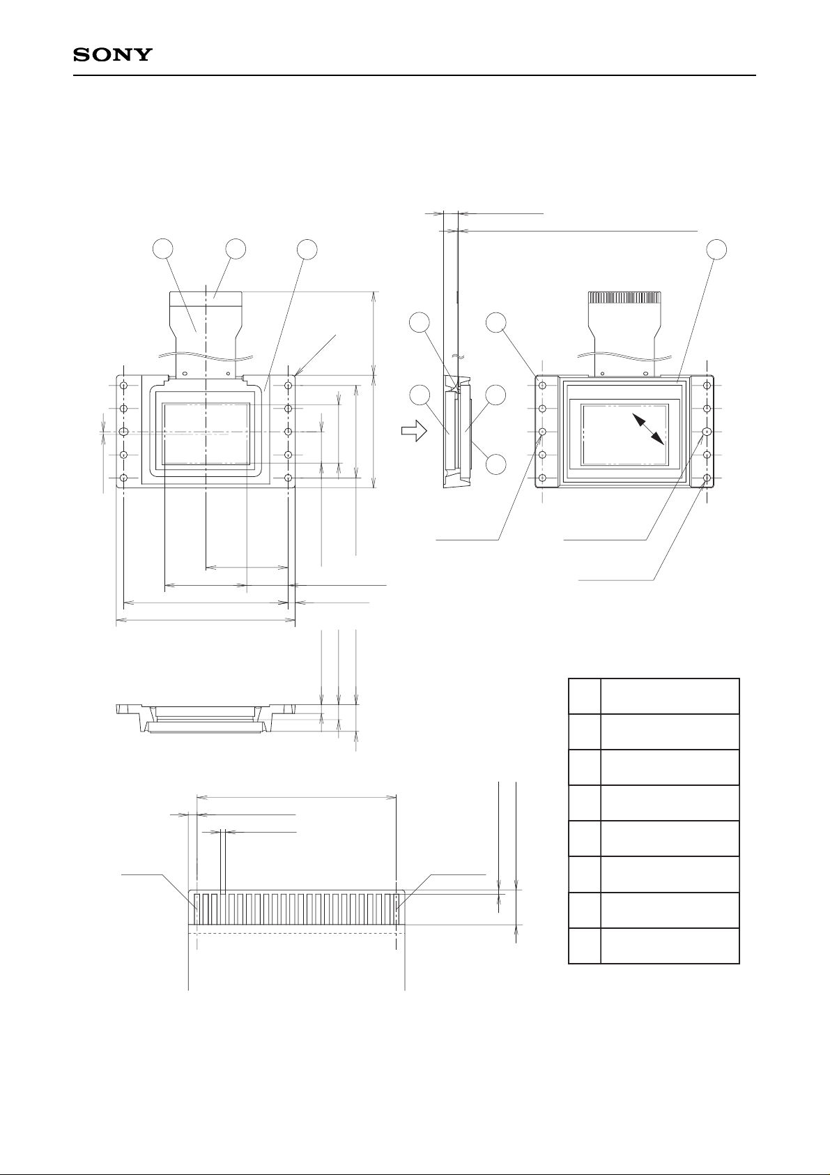
Package Outline Unit: mm
3.0 ± 0.2
5.1 ± 0.2
9.2 ± 0.2
(5.1)
φ2.5H9
8-φ2.5 ± 0.1
2.5H9 × 3.0
Active Area
Thickness of the connector 0.3 ± 0.05
Incident
light
3
4
5
6
7
Glass
Polarizing film
electrode (enlarged)
P 1.0 × 23 = 23.0 ± 0.1
0.6 ± 0.05
1.0 ± 0.15
0.5 ± 0.15
4.0 ± 0.4
PIN24
PIN1
The rotation angle of the active area relative to H and V is ± 1°.
weight 45g
Description
Molding material
Outside frame
Reinforcing board
Reinforcing material
F P C
No
1
2
3
4
5
6
7
6
(28.5)
P 8.0 × 4 = 32.0 ± 0.2
39.0 ± 0.2
61.9 ± 0.7
2.5 ± 0.2
57.0 ± 0.2
62.0 ± 0.2
4-R1.0
1
2
3
Polarizing
Axis
(0.9)
8.60 ± 0.25
(20.05)
(26.87)
15.06 ± 0.25
 Loading...