

Sony LCX016AL Datasheet

LCX016AL
For the availability of this product, please contact the sales office.
3.3cm (1.3-inch) Black-and-White LCD Panel
Description
The LCX016AL is a 3.3cm diagonal active matrix
TFT-LCD panel addressed by polycrystalline silicon
super thin film transistors with a built-in peripheral
driving circuit. Use of three LCX016AL panels
provides a full-color representation. The striped
arrangement suitable for data projectors is capable
of displaying fine text and vertical lines.
The adoption of an advanced on-chip black matrix
realizes high picture quality without cross talk by
incorporating a high luminance screen and cross
talk free circuit.
This panel has a polysilicon TFT high-speed
scanner and built-in function to display images
up/down and/or right/left inverse. The built-in 5V
interface circuit leads to lower voltage of timing and
control signals.
The panel contains an active area variable circuit
which supports Macintosh17∗1/SVGA/VGA/PC98
data signals by changing the active area according
to the type of input signal. In addition, double-speed
processed NTSC/PAL can also be supported.
∗1
“Macintosh” is a treadmark of Apple Computer, Inc.
∗2
“PC98” is a treadmark of NEC Corporation.
∗2
Features
• Number of active dots: 519,000 (1.3-inch, 3.3cm in diagonal)
• Accepts the computer requirements of Macintosh17 (832 × 624), SVGA (800 × 600), VGA (640 × 480)
and PC98 (640 × 400) platforms
• Supports NTSC (640 × 480) and PAL (762 × 572) by processing the video signal at double speed
• High optical transmittance: 20% (typ.)
• Built-in cross talk free circuit
• High contrast ratio with normally white mode: 200 (typ.)
• Built-in H and V drivers (built-in input level conversion circuit, 5V driving possible)
• Up/down and/or right/left inverse display function
Element Structure
• Dots: 832 (H) × 624 (V) = 519,168
• Built-in peripheral driver using polycrystalline silicon super thin film transistors
Applications
• Liquid crystal data projectors
• Liquid crystal projectors, etc.
Sony reserves the right to change products and specifications without prior notice. This information does not convey any license by
any implication or otherwise under any patents or other right. Application circuits shown, if any, are typical examples illustrating the
operation of the devices. Sony cannot assume responsibility for any problems arising out of the use of these circuits.
– 1 –
E96220-ST
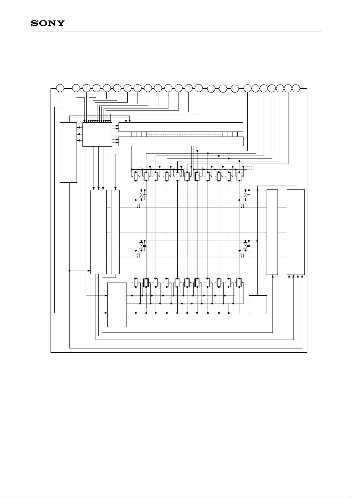
Block Diagram
PSIG
1
13
HST
HCK1
14 15
HCK2
17
BLK
9
RGT
20
VST
19
VCK
21
PCG
22
DWN
18
ENB
MODE1
12
MODE2
11
MODE3
10
LCX016AL
DD
DD
HV
8
23
VV
Vss
16
SIG1
7
SIG2
5
SIG3
3
SIG4
2
4
SIG5
6
SIG6
24
COM
Input Signal
Level Shifter
Circuit
Inversion Control Circuit
Up/Down and/or Right/Left
(Bidirectional Scanning)
V Shift Register
Black Frame Control Circuit
H Shift Register (Bidirectional Scanning)
Black Frame Control Circuit
(Bidirectional Scanning)
Black Frame Control Circuit
V Shift Register
Circuit
Precharge Control
COM
PAD
– 2 –
LCX016AL
Absolute Maximum Ratings (VSS = 0V)
• H driver supply voltage HVDD –1.0 to +20 V
• V driver supply voltage VVDD –1.0 to +20 V
• Common pad voltage COM –1.0 to +17 V
• H shift register input pin voltage HST, HCK1, HCK2, –1.0 to +17 V
RGT
• V shift register input pin voltage VST, VCK, PCG, –1.0 to +17 V
BLK, ENB, DWN
MODE1, MODE2, MODE3
• Video signal input pin voltage SIG1, SIG2, SIG3, SIG4, –1.0 to +15 V
SIG5, SIG6, PSIG
• Operating temperature Topr –10 to +70 °C
• Storage temperature Tstg –30 to +85 °C
Operating Conditions (VSS = 0V)
• Supply voltage
HVDD 15.5 ± 0.3V
VVDD 15.5 ± 0.3V
• Input pulse voltage (Vp-p of all input pins except video signal and uniformity improvement signal input pins)
Vin 5.0 ± 0.5V
Pin Description
Pin
No.
1
2
3
4
5
6
7
8
9
Symbol Description
PSIG
SIG4
SIG3
SIG5
SIG2
SIG6
SIG1
HVDD
RGT
Uniformity improvement signal
Video signal 4 to panel
Video signal 3 to panel
Video signal 5 to panel
Video signal 2 to panel
Video signal 6 to panel
Video signal 1 to panel
Power supply for H driver
Drive direction pulse for H shift
register (H: normal, L: reverse)
Pin
No.
13
14
15
16
17
18
19
20
21
Symbol Description
HST
HCK1
HCK2
Vss
BLK
ENB
VCK
VST
PCG
Start pulse for H shift register
drive
Clock pulse for H shift register
drive
Clock pulse for H shift register
drive
GND (H, V drivers)
Black Frame display pulse
Enable pulse for gate selection
Clock pulse for V shift register
drive
Start pulse for V shift register
drive
Improvement pulse for uniformity
10
11
12
MODE3
MODE2
MODE1
Display area switching 3
Display area switching 2
Display area switching 1
– 3 –
22
23
24
DWN
VVDD
COM
Drive direction pulse for V shift
register (H: normal, L: reverse)
Power supply for V driver
Common voltage of panel
LCX016AL
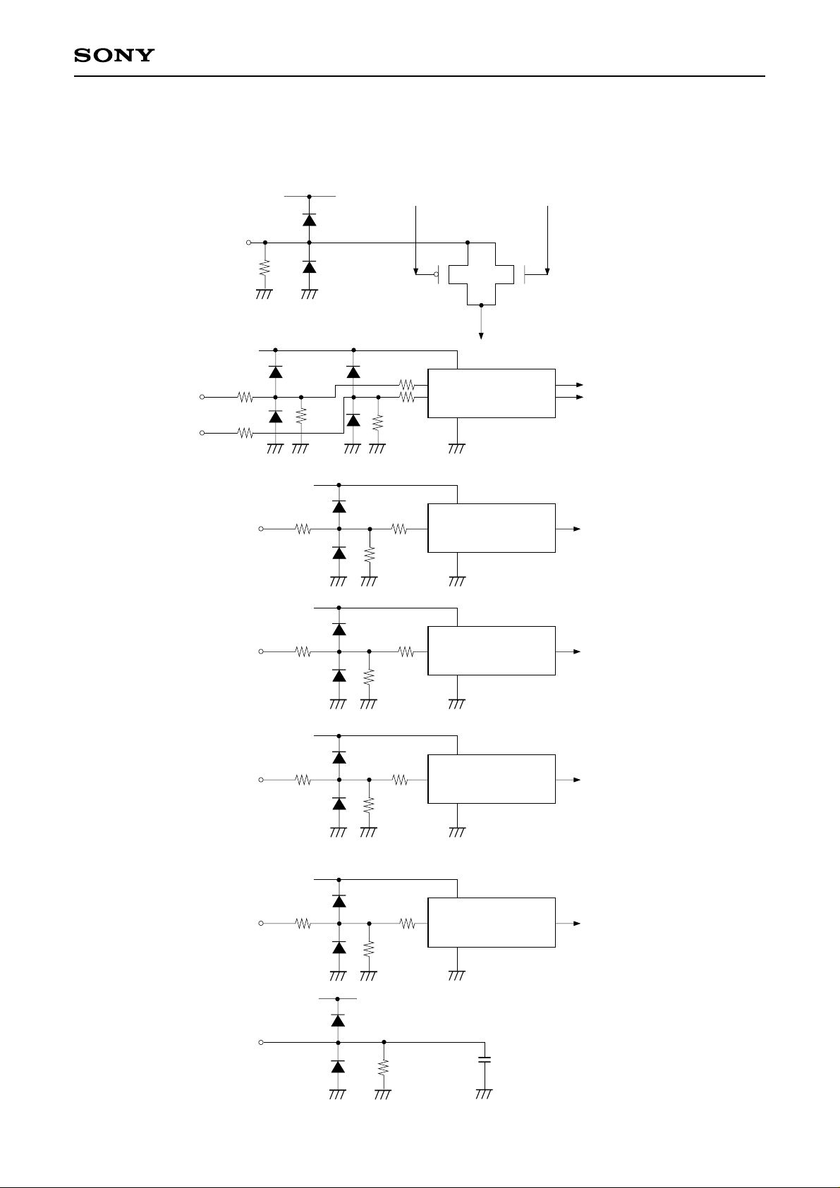
Input Equivalent Circuit
To prevent static charges, protective diodes are provided for each pin except the power supplies. In addition,
protective resistors are added to all pins except the video signal inputs. All pins are connected to VSS with a
high resistor of 1MΩ (typ.). The equivalent circuit of each input pin is shown below: (Resistance value: typ.)
(1) SIG1, SIG2, SIG3, SIG4, SIG5, SIG6, PSIG
DD
HV
Input
1MΩ
(2) HCK1, HCK2
(3) RGT
(4) HST
(5) PCG, VCK
Input
HV
Input
Input
DD
250Ω
250Ω
HV
HV
VV
DD
DD
DD
1MΩ
1MΩ
2.5kΩ2.5kΩ
1MΩ
1MΩ
250Ω
Level conversion circuit
250Ω
250Ω250Ω
(2-phase input)
Level conversion circuit
(single-phase input)
Level conversion circuit
(single-phase input)
Signal line
250Ω250Ω
Input
1MΩ
(6) VST, BLK, ENB, DWN, MODE1, MODE2, MODE3
DD
VV
2.5kΩ2.5kΩ
Input
1MΩ
(7) COM
Input
VVDD
1MΩ
Level conversion circuit
(single-phase input)
Level conversion circuit
(single-phase input)
LC
– 4 –
Input Signals
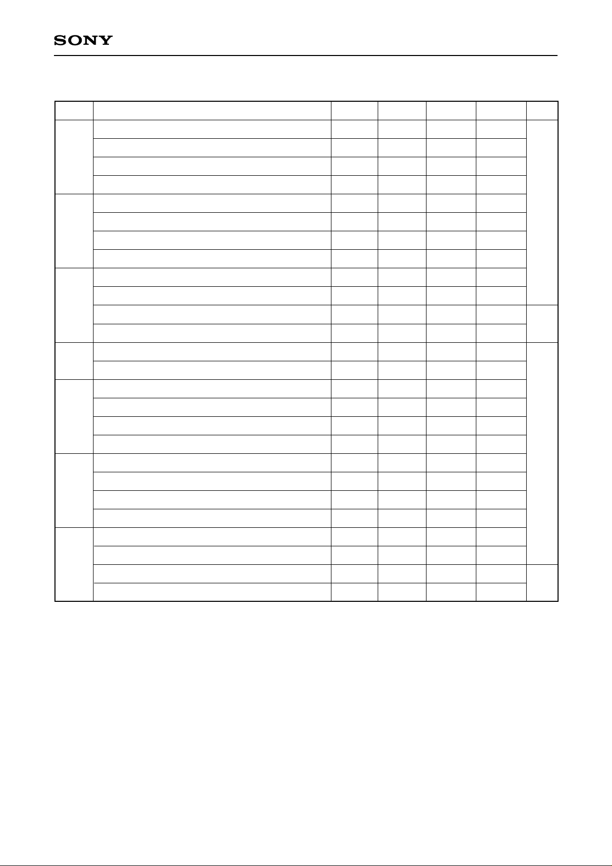
1. Input signal voltage conditions (VSS = 0V)
LCX016AL
Item
H shift register input voltage
HST, HCK1, HCK2, RGT
V shift register input voltage
(Low)
(High)
(Low)
MODE1, MODE2, MODE3,
BLK, VST, VCK, PCG,
ENB, DWN
(High)
Video signal center voltage
Video signal input range
Common voltage of panel
∗1
∗2
Uniformity improvement signal
input voltage (PSIG)
∗1
Input video signal shall be symmetrical to VVC.
∗2
The typical value of the common pad voltage may lower its suitable voltage according to the set
∗3
Symbol Min. Typ. Max. Unit
VHIL
VHIH
VVIL
VVIH
VVC
Vsig
Vcom
Vpsig
–0.5
4.5
–0.5
4.5
6.8
VVC – 4.5
VVC – 0.5
VVC ± 4.3
0.0
5.0
0.0
5.0
7.0
7.0
VVC – 0.4
VVC ± 4.5
0.4
5.5
0.4
5.5
7.2
VVC + 4.5
VVC – 0.3
VVC ± 4.7
V
V
V
V
V
V
V
V
construction to use. In this case, use the voltage of which has maximum contrast as typical value.
When the typical value is lowered, the maximum and minimum values may lower.
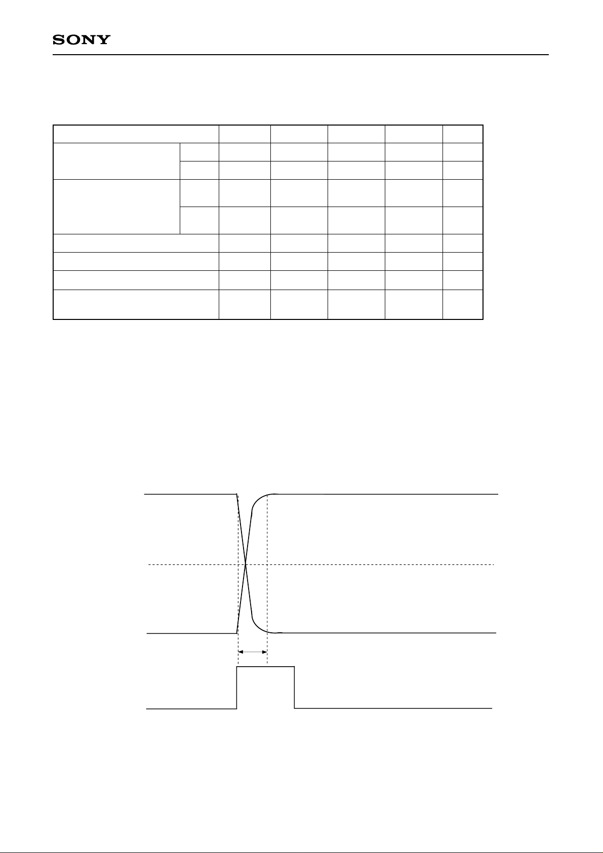
∗3
Input a uniformity improvement signal PSIG in the same polarity with video signals SIG1 to 6 and which is
symmetrical to VVC. Also, the rising and falling of PSIG are synchronized with the rising of PCG pulse, and
the rise time trPSIG and fall time tfPSIG are suppressed within 800ns (as shown in a diagram below).
Input waveform of uniformity improvement signal PSIG
90%
PSIG
10%
trPSIG
tfPSIG
PCG
VVC
Level Conversion Circuit
The LCX016AL has a built-in level conversion circuit in the clock input unit on the panel. The input signal level
increases to HVDD or VVDD. The VCC of external ICs are applicable to 5 ± 0.5V.
– 5 –
LCX016AL
2. Clock timing conditions (Ta = 25°C) (Macintosh17 mode: fHCKn = 4.8MHz, fVCK = 24.9kHz)
Item Symbol Min. Typ. Max. Unit
HST
HCK
VST
VCK
ENB
PCG
BLK
Hst rise time
Hst fall time
Hst data set-up time
Hst data hold time
Hckn rise time
Hckn fall time
∗4
∗4
Hck1 fall to Hck2 rise time
Hck1 rise to Hck2 fall time
Vst rise time
Vst fall time
Vst data set-up time
Vst data hold time
Vck rise time
Vck fall time
Enb rise time
Enb fall time
Vck rise/fall to Enb rise time
Enb pulse width
Pcg rise time
Pcg fall time
Pcg fall to Vck rise/fall time
Pcg pulse width
Blk rise time
Blk fall time
∗5
Blk fall to Vst rise time
Blk pulse width
trHst
tfHst
tdHst
thHst
trHckn
tfHckn
to1Hck
to2Hck
trVst
tfVst
tdVst
thVst
trVck
tfVck
trEnb
tfEnb
tdEnb
twEnb
trPcg
tfPcg
toVck
twPcg
trBlk
tfBlk
toVst
twBlk
—
—
70
15
—
—
–15
–15
—
—
5
5
—
—
—
—
400
2400
—
—
900
1100
—
—
32
20
—
—
80
25
—
—
0
0
—
—
10
10
—
—
—
—
500
2500
—
—
1000
1200
—
—
33
21
30
30
90
35
30
ns
30
15
15
100
100
15
µs
15
100
100
100
100
600
2600
ns
30
30
1100
1300
100
100
34
µs
22
∗4
Hckn means Hck1 and Hck2.
∗5
Blk is the timing during SVGA mode (fHckn = 4.0MHz, fVck = 24.0kHz).
– 6 –
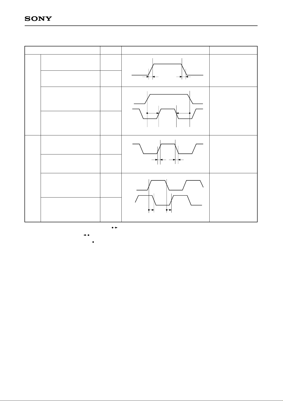
<Horizontal Shift Register Driving Waveform>
Item Symbol Waveform Conditions
LCX016AL
HST
HCK
Hst rise time
Hst fall time
Hst data set-up time
Hst data hold time
Hckn rise time
Hckn fall time
∗3
∗3
Hck1 fall to Hck2 rise time
trHst
tfHst
tdHst
thHst
trHckn
tfHckn
to1Hck
Hst
∗
6
Hst
Hck1
Hckn
∗
6
Hck1
90%
10%
trHst tfHst
50%
50%
tdHst thHst
90%
∗
3
10%
trHckn tfHckn
50%
90%
50%
50%
90%
10%
10%
50%
∗3
• Hckn
duty cycle 50%
to1Hck = 0ns
to2Hck = 0ns
∗3
• Hckn
duty cycle 50%
to1Hck = 0ns
to2Hck = 0ns
∗3
• Hckn
duty cycle 50%
to1Hck = 0ns
to2Hck = 0ns
50%
to2Hck to1Hck
Hck1 rise to Hck2 fall time
∗6
Definitions: The right-pointing arrow ( ) means +.
to2Hck
Hck2
The left-pointing arrow ( ) means –.
The black dot at an arrow ( ) indicates the start of measurement.
50%
– 7 –
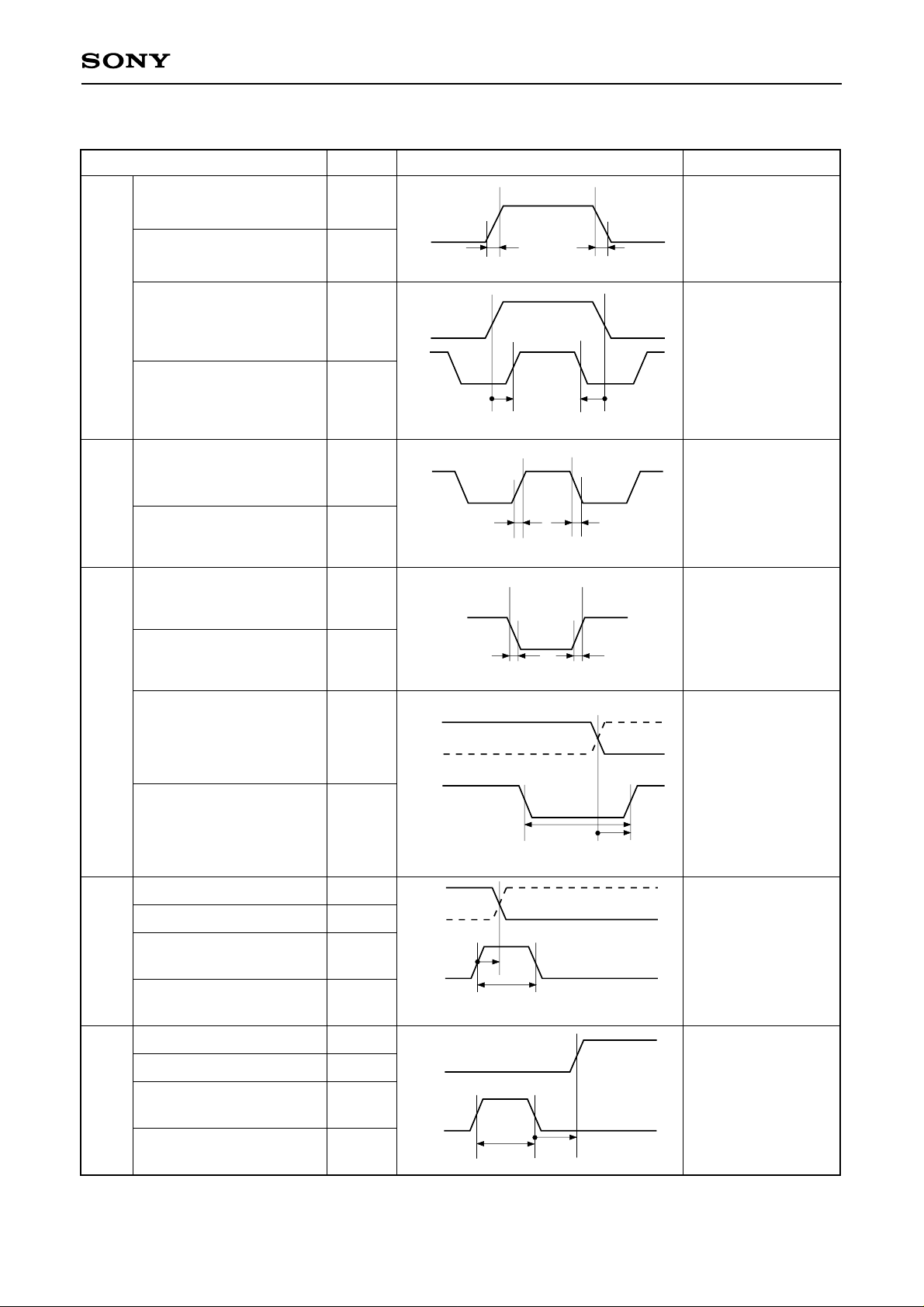
<Vertical Shift Register Driving Waveform>
Item Symbol Waveform Conditions
LCX016AL
VST
VCK
Vst rise time
Vst fall time
Vst data set-up time
Vst data hold time
Vck rise time
Vck fall time
Enb rise time
Enb fall time
trVst
tfVst
tdVst
thVst
trVck
tfVck
trEnb
tfEnb
Vst
∗
Vst
Vck
Vck
90%
10%
trVst tfVst
6
50%
50%
tdVst thVst
90%
10%
trVckn tfVckn
90%
10%
Enb
tfEn trEn
90%
10%
10%
50%
50%
90%
10%
90%
ENB
PCG
BLK
Vck rise/fall to Enb rise
time
Enb pulse width
Pcg rise time
Pcg fall time
∗7
Pcg rise to Vck rise/fall
time
Pcg pulse width
Blk rise time
Blk fall time
Blk fall to Vst rise time
Blk pulse width
tdEnb
twEnb
trPcg
tfPcg
toVck
trPcg
twBlk
tfBlk
toVst
twBlk
Vck
Enb
∗
Vck
Pcg
∗
Vst
Blk
∗
50%
50%
6
toVck
50%
6
6
twPcg
50%
twBlk
twEnb
50%
50%
50%
50%
toVst
50%
tdEnb
∗7
Input the pulse obtained by taking the OR of the above pulse (PCG) and BLK to the PCG input pin.
– 8 –
 Loading...