

Sony LCX007BK Datasheet

3.4cm (1.35-inch) Color LCD Panel
Description
The LCX007AK is a 3.4cm diagonal active matrix
TFT-LCD panel addressed by polycrystalline silicon
super thin film transistors with built-in peripheral driving
circuit, and it provides a full-color representation is
possible.
This panel provides a wide aspect ratio of 16:9,
such as those represented in HD. The built-in sideblack function also allows an aspect ratio of 4:3 in
the NTSC/PAL mode.
This panel has a polysilicon TFT high-speed
scanner and built-in function to display images
up/down and/or right/left inverse. The built-in 5V
interface circuit leads to lower voltage of timing
system and control signals.
LCX007BK
Features
• The number of active dots: 512,880 (1.35-inch; 3.4cm in diagonal)
• Horizontal resolution: 400 TV lines
• High optical transmittance: 4.0% (typ.)
• High contrast ratio with normally white mode: 190 (typ.)
• Built-in H and V drivers (built-in input level conversion circuit, 5V driving possible)
• NTSC/NTSC-WIDE/HD (band: 20MHz) mode selectable
(PAL/PAL-WIDE mode also available through conversion of scanned dot numbers by an external IC)
• Up/down and/or right/left inverse display function
• Side-black function
• 16:9 and 4:3 aspect-ratio switching function
• Full-color display
Element Structure
• Dots
16:9 display: 1068.5 (H) × 480 (V) = 512,880
4:3 display: 799.5 (H) × 480 (V) = 383,760
• Built-in peripheral driver using polycrystalline silicon super thin film transistors.
Applications
Liquid crystal projectors, etc.
Sony reserves the right to change products and specifications without prior notice. This information does not convey any license by
any implication or otherwise under any patents or other right. Application circuits shown, if any, are typical examples illustrating the
operation of the devices. Sony cannot assume responsibility for any problems arising out of the use of these circuits.
– 1 –
E95733A64-ST
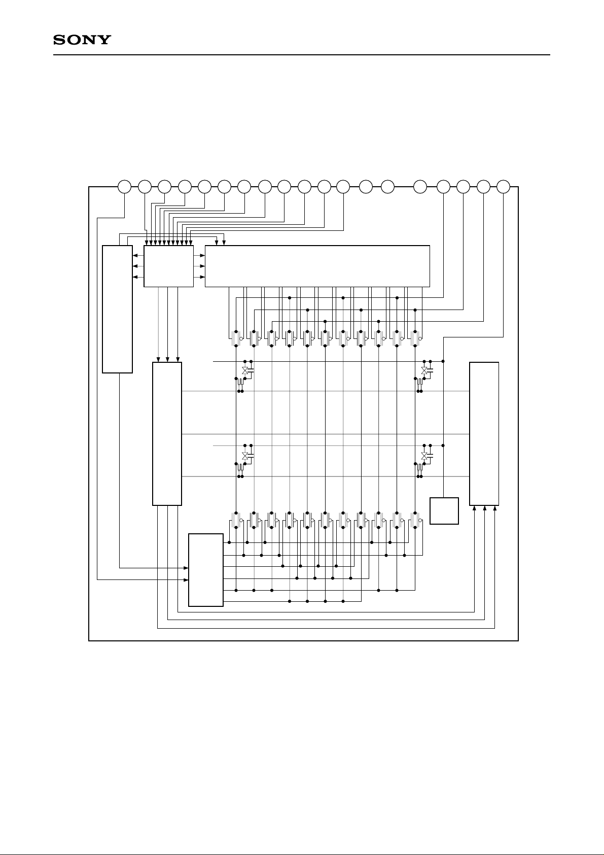
Block Diagram
1
SID
8
HST
10
HCK1
11
HCK2
6
WID
RGT
7 16
VST
VCK
1514
PCG
17
DWN
13
ENB
12
CLR
LCX007BK
DD
DD
VV
HV
18
5
SS
V
SIG1(G)
9
2
SIG2(R)
3
SIG3(B)
19
4
COM
Input Signal
Level Shifter
4 : 3/16 : 9
Control Circuit
Up/Down or Right/Left Inversion
V Shift Register
(Bidirectional Scanning)
H Shift Register (Bidirectional Scanning)
V Shift Register
(Bidirectional Scanning)
COM
Pad
Side Black
Control Circuit
– 2 –
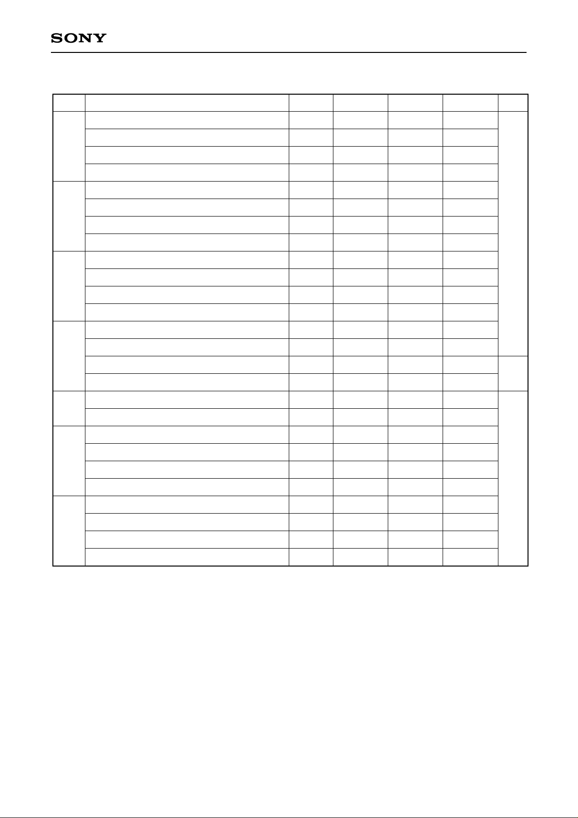
Absolute Maximum Ratings (VSS = 0V)
• H driver supply voltage HVDD –1.0 to +20 V
• V driver supply voltage VVDD –1.0 to +20 V
• Common pad voltage COM –1.0 to +17 V
• H shift register input pin voltage HST, HCK1, HCK2 –1.0 to +17 V
RGT, WID
• V shift register input pin voltage VST, VCK, PCG –1.0 to +17 V
CLR, ENB, DWN
• Video signal input pin voltage SIG1, SIG2, SIG3, SID –1.0 to +15 V
• Operating temperature Topr –10 to +70 °C
• Storage temperature Tstg –30 to +85 °C
Operating Conditions (VSS = 0V)
• Supply voltage
HVDD 15.7 V
VVDD 15.7 V
+0.3
–0.4
+0.3
–0.4
• Input pulse voltage (Vp-p of all input pins except video signal and side black signal input pins)
Vin 5.0 ± 0.5 V
LCX007BK
Pin Description
Pin
No.
1
2
3
4
5
6
7
8
Symbol Description
SID
SIG1 (G)
SIG2 (R)
SIG3 (B)
HVDD
WID
RGT
HST
Side black signal for 4:3 display
Video signal (G) to panel
Video signal (R) to panel
Video signal (B) to panel
Power supply for H driver
Aspect-ratio switching
(H: 16:9, L: 4:3)
Drive direction pulse for H shift
register (H: normal, L: reverse)
Start pulse for H shift register
drive
Pin
No.
11
12
13
14
15
16
17
18
Symbol Description
HCK2
CLR
ENB
VCK
PCG
VST
DWN
VVDD
Clock pulse for H shift register
drive
Improvement pulse (1) for
uniformity
Enable pulse for gate selection
Clock pulse for V shift register
drive
Improvement pulse (2) for
uniformity
Start pulse for V shift register
drive
Drive direction pulse for V shift
register (H: normal, L: reverse)
Power supply for V driver
9
10
Vss
HCK1
GND (H, V drivers)
Clock pulse for H shift register
drive
– 3 –
19
20
COM
TEST
Common voltage of panel
Test; Open
LCX007BK
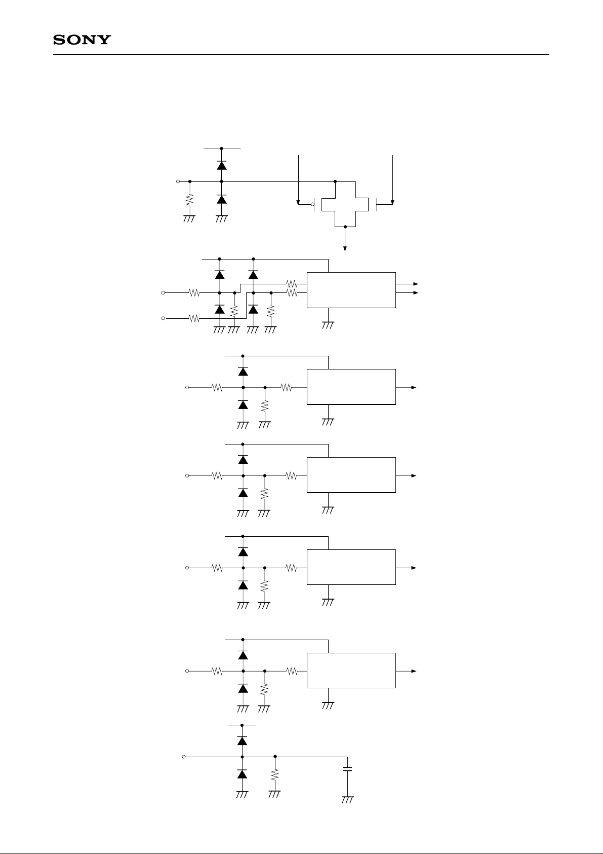
Input Equivalent Circuit
To prevent static charges, protective diodes are provided for each pin except the power supply. In addition,
protective resistors are added to all pins except video signal input. All pins are connected to Vss with a high
resistance of 1MΩ (typ.). The equivalent circuit of each input pin is shown below: (The resistor value: typ.)
(1) SIG1, SIG2, SIG3, SID
HV
DD
Input
1MΩ
(2) HCK1, HCK2
(3) RGT, WID
(4) HST
(5) PCG, VCK
Input
Input
Input
HV
DD
250Ω
250Ω
HV
HV
VV
DD
DD
DD
1MΩ
1MΩ
2.5kΩ2.5kΩ
1MΩ
1MΩ
250Ω
Level conversion circuit
250Ω
250Ω250Ω
(2-phase input)
Level conversion circuit
(single-phase input)
Level conversion circuit
(single-phase input)
Signal line
Input
(6) VST, CLR, ENB, DWN
Input
(7) COM
Input
VV
VVDD
DD
1MΩ
1MΩ
250Ω250Ω
Level conversion circuit
(single-phase input)
2.5kΩ2.5kΩ
Level conversion circuit
(single-phase input)
1MΩ
– 4 –
LC
Input Signals
1. Input signal voltage conditions (VSS = 0V)
LCX007BK
Item
H driver input voltage
WID, RGT, HST, HCK1, HCK2
V driver input voltage
CLR, ENB, VCK, PCG, VST, DWN
(Low)
(High)
(Low)
(High)
Video signal center voltage
Video signal input range
Common voltage of panel
∗1
Video input signal shall be symmetrical to VVC.
∗2
Common voltage of the panel shall be adjusted to VVC – 0.4V.
∗1
∗2
Symbol Min. Typ. Max. Unit
VHIL
VHIH
VVIL
VVIH
VVC
Vsig
Vcom
–0.5
4.5
–0.5
4.5
6.5
VVC – 4.5
VVC – 0.5
0.0
5.0
0.0
5.0
7.0
—
VVC – 0.4
0.3
5.5
0.3
5.5
7.2
VVC + 4.5
VVC – 0.3
V
V
V
V
V
V
V
Level Conversion Circuit
The LCX007BK has a built-in level conversion circuit in the clock input unit on the panel. The input signal level
increases to HVDD or VVDD. The VCC of external ICs are applicable to 5 ± 0.5V.
– 5 –
LCX007BK
2. Clock timing conditions (Ta = 25°C) (fHCKn = 7.5MHz, fVCK = 15.7kHz)
Item Symbol Min. Typ. Max. Unit
HST
HCK
CLR
VST
VCK
Hst rise time
Hst fall time
Hst data set-up time
Hst data hold time
Hckn∗3rise time
Hckn∗3fall time
Hck1 fall to Hck2 rise time
Hck1 rise to Hck2 fall time
Clr rise time
Clr fall time
Clr pulse width
Vck rise/fall to Clr fall time
Vst rise time
Vst fall time
Vst data set-up time
Vst data hold time
Vck rise time
Vck fall time
trHst
tfHst
tdHst
thHst
trHckn
tfHckn
to1Hck
to2Hck
trClr
tfClr
twClr
tdClr
trVst
tfVst
tdVst
thVst
trVck
tfVck
—
—
20
–40
—
—
–15
–15
—
—
3000
–50
—
—
–25
5
—
—
—
—
67
0
—
—
0
0
—
—
3100
0
—
—
15
15
—
—
30
30
100
40
30
30
15
ns
15
100
100
3200
50
100
100
25
µs
25
100
100
Enb rise time
Enb fall time
ENB
Vck rise/fall to Enb rise time
Enb pulse width
Pcg rise time
Pcg fall time
PCG
Pcg fall to Vck rise/fall time
Pcg pulse width
∗3
Hckn means Hck1 and Hck2.
trEnb
tfEnb
tdEnb
twEnb
trPcg
tfPcg
toVck
twPcg
—
—
350
3450
—
—
650
1150
—
—
400
3500
—
—
700
1200
100
100
450
3550
20
20
750
1250
ns
– 6 –
<Horizontal Shift Register Driving Waveform>
Item Symbol Waveform Conditions
LCX007BK
HST
HCK
Hst rise time
Hst fall time
Hst data set-up time
Hst data hold time
Hckn∗3rise time
Hckn∗3fall time
Hck1 fall to Hck2 rise
time
trHst
tfHst
tdHst
thHst
trHckn
tfHckn
to1Hck
Hst
∗4
Hst
Hck1
Hckn
∗4
Hck1
90%
10%
trHst tfHst
50%
50%
tdHst thHst
90%
∗3
10%
trHckn tfHckn
50%
90%
50%
50%
90%
10%
10%
50%
O Hckn
∗3
duty cycle 50%
to1Hck = 0ns
to2Hck = 0ns
O Hckn
∗3
duty cycle 50%
to1Hck = 0ns
to2Hck = 0ns
O Hckn
∗3
duty cycle 50%
to1Hck = 0ns
to2Hck = 0ns
CLR
Hck1 rise to Hck2 fall
time
Clr rise time
Clr fall time
Clr pulse width
Vck rise/fall to Clr fall
time
to2Hck
trClr
tfClr
twClr
tdClr
Hck2
Clr
Vck
Clr
∗4
50%
to2Hck to1Hck
90%
10%
trClr tfClr
50%
50%
twClr
50%
90%
50%
tdClr
10%
O Hckn
∗3
duty cycle 50%
to1Hck = 0ns
to2Hck = 0ns
– 7 –
<Vertical Shift Register Driving Waveform>
Item Symbol Waveform Conditions
LCX007BK
VST
VCK
Vst rise time
Vst fall time
Vst data set-up time
Vst data hold time
Vck rise time
Vck fall time
Enb rise time
Enb fall time
trVst
tfVst
tdVst
thVst
trVck
tfVck
trEnb
tfEnb
Vst
∗4
Vst
Vck
Vck
90%
10%
trVst tfVst
50%
50%
tdVst thVst
90%
10%
trVckn tfVckn
90%
10%
Enb
tfEn trEn
90%
50%
10%
10%
50%
90%
10%
90%
ENB
Vck rise/fall to Enb rise
time
Enb pulse width
tdEnb
twEnb
Vck
Enb
Pcg rise time trPcg
Vck
Pcg fall time tfPcg
PCG
Pcg fall to Vck rise/fall
time
toVck
Pcg
50%
Pcg pulse width twPcg
∗4
Definitions: The right-pointing arrow ( ) means +.
The left-pointing arrow ( ) means –.
The black dot at an arrow ( ) indicates the start of measurement.
50%
twEnb
50%
twPcg toVck
tdEnb
50%
50%
50%
∗4
∗4
– 8 –
 Loading...