

Sony LCX005BK Datasheet

LCX005BK
For the availability of this product, please contact the sales office.
1.4cm (0.55-inch) NTSC/PAL Color LCD Panel
Description
The LCX005BK is a 1.4cm diagonal active matrix
TFT-LCD panel addressed by polycrystalline silicon
super thin film transistors with built-in peripheral
driving circuit. This panel provides full-color
representation in NTSC/PAL mode. RGB dots are
arranged in a delta pattern featuring high picture
quality of no fixed color patterns, which is inherent in
vertical stripes and mosaic pattern arrangements.
Features
• The number of active dots: 113,578 (0.55-inch; 1.397cm in diagonal)
• Horizontal resolution: 260 TV lines
• High optical transmittance: 3.4% (typ.)
• High contrast ratio with normally white mode: 270 (typ.)
• Built-in H and V drivers (built-in input level conversion circuit, TTL drive possible)
• High quality picture representation with RGB delta arranged color filters
• Full-color representation
• NTSC/PAL compatible
• Right/left inverse display function
Element Structure
• Dots
Total dots : 537 (H) × 222 (V) = 119,214
Active dots: 521 (H) × 218 (V) = 113,578
• Built-in peripheral driver using polycrystalline silicon super thin film transistors.
Applications
• Viewfinders
• Super compact liquid crystal monitors etc.
Sony reserves the right to change products and specifications without prior notice. This information does not convey any license by
any implication or otherwise under any patents or other right. Application circuits shown, if any, are typical examples illustrating the
operation of the devices. Sony cannot assume responsibility for any problems arising out of the use of these circuits.
– 1 –
E94Z24A5X-PS
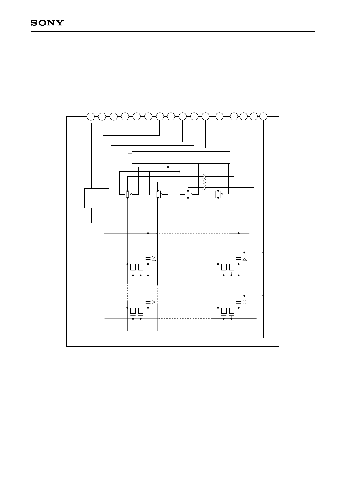
Block Diagram
16
DD
V
SS
V
15
H Level
Conversion
VST
14
Circuit
13
VCK2
12
VCK1
11
EN
CLR
10
RGT
HST
9
8
H Shift Register
HCK2
7
HCK1
6
(NC)
5
BLUE
4
3
RED
GREEN
2
LCX005BK
COM
1
V Level
Conversion
Circuit
V Shift Register
CS LC
COM
Pad
– 2 –
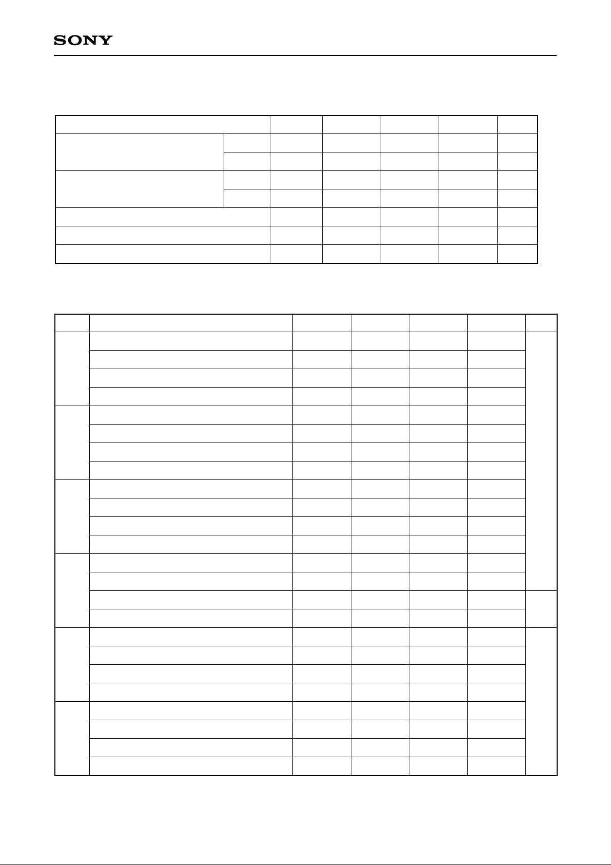
Absolute Maximum Ratings (VSS = 0V)
• H and V driver supply voltages VDD –1.0 to +17 V
• H driver input pin voltage HST, HCK1, HCK2 –1.0 to +17 V
RGT
• V driver input pin voltage VST, VCK1, VCK2 –1.0 to +17 V
CLR, EN
• Video signal input pin voltage GREEN, RED, BLUE –1.0 to +15 V
• Operating temperature Topr –10 to +70 °C
• Storage temperature Tstg –30 to +85 °C
Operating Conditions (VSS = 0V)
Supply voltage
VDD 13.5 ± 0.5 V
Input pulse voltage (Vp-p of all input pins except video signal input pins)
Vin 2.8V (more than)
Pin Description
LCX005BK
Pin
No.
1
2
3
4
(5)
6
7
8
Symbol Description
COM
GREEN
RED
BLUE
(NC)
HCK1
HCK2
HST
Common voltage of panel
Video signal (G) to panel
Video signal (R) to panel
Video signal (B) to panel
Not connected
Clock pulse for H shift register
drive
Clock pulse for H shift register
drive
Start pulse for H shift register
drive
Pin
No.
9
10
11
12
13
14
15
16
Symbol Description
RGT
CLR
EN
VCK1
VCK2
VST
Vss
VDD
Drive direction pulse for H shift
register (H: normal, L: reverse)
Improvement pulse for
uniformity
Enable pulse for gate selection
Clock pulse for V shift register
drive
Clock pulse for V shift register
drive
Start pulse for V shift register
drive
GND (H, V drivers)
Power supply for H and V drivers
– 3 –
LCX005BK
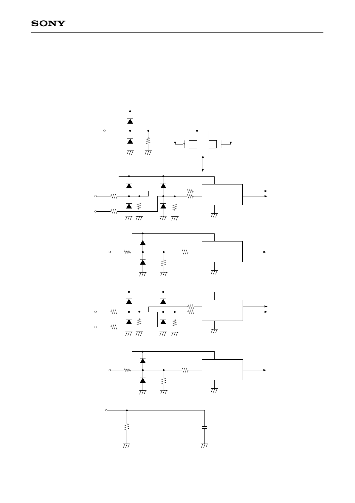
Input Equivalent Circuit
To prevent static charges, protective diodes are provided for each pin except the power supply. In addition,
protective resistors are added to all pins except video signal input. All pins are connected to Vss with a high
resistance of 1MΩ (typ.). The equivalent circuit of each input pin is shown below: (The resistor value: typ.)
(1) Video signal input
From H driver
Input
V
DD
1MΩ
(2) HCK1, HCK2
(3) HST
(4) VCK1, VCK2
HCK1
HCK2
VCK1
VCK2
Input
V
DD
250Ω
250Ω
VDD
2.5kΩ
1kΩ
Signal line
250Ω
1MΩ
V
DD
1MΩ
250Ω
1MΩ
250Ω250Ω
1MΩ
2.5kΩ
1MΩ
1kΩ
Level conversion
circuit (2-phase
input)
Level conversion
circuit (singlephase input)
Level conversion
circuit (2-phase
input)
(5) RGT, VST, CLR, EN
(6) COM
Input
Input
DD
V
2.5kΩ
1MΩ
1MΩ
– 4 –
2.5kΩ
Level conversion
circuit (singlephase input)
LC
LCX005BK
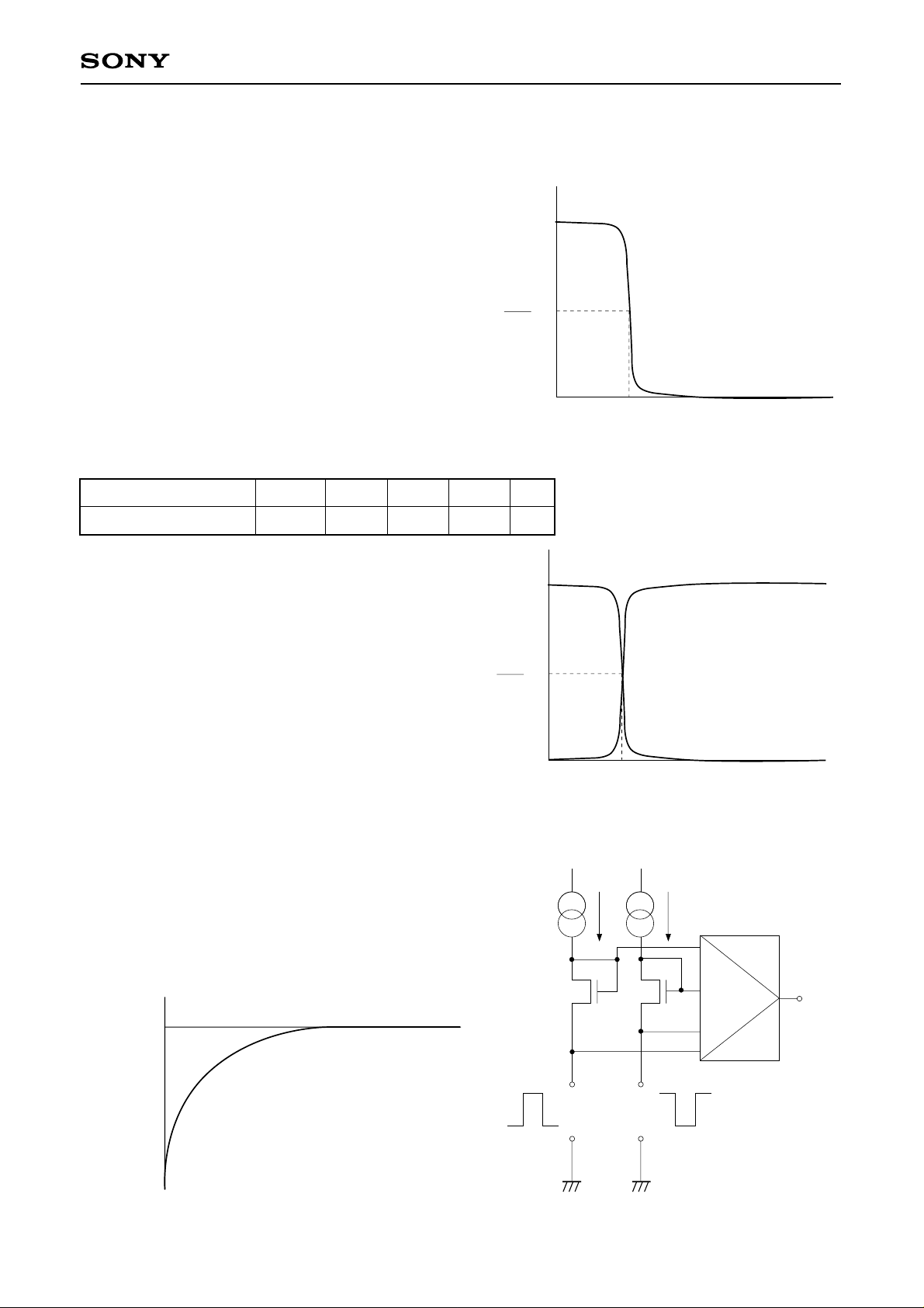
Level Conversion Circuit
The LCX005BK has a built-in level conversion circuit in the clock input unit located inside the panel. The circuit
voltage is stepped up to VDD inside the panel. This level conversion circuit meets the specifications of a 3.0V to
5.0V power supply of the externally-driven IC.
1. I/O characteristics of level conversion circuit
VDD
(For a single-phase input unit)
An example of the I/O voltage characteristics of a
level conversion circuit is shown in the figure to the
right. The input voltage value that becomes half the
VDD
2
output voltage (after voltage conversion) is defined
as Vth.
The Vth value varies depending on the VDD voltage.
Output voltage (inside panel)
The Vth values under standard conditions are
indicated in the table below. (HST, VST, EN, CLR,
and RGT in the case of a single-phase input)
VDD = 13.5V
Item
Symbol Min. Typ. Max. Unit
Vth voltage of circuit Vth 0.4 1.50 2.75 V
(For a differential input unit)
VDD
An example of I/O voltage characteristics of a level
conversion circuit for a differential input is shown in
the figure to the right. Although the characteristics,
including those of the Vth voltage, are basically the
VDD
2
same as those for a single-phased input, the twophased input phase is defined. (Refer to clock
Output voltage (inside panel)
timing conditions.)
2. Current characteristics at the input pin of level conversion circuit
Example of single-phase
I/O characteristics
Vth
Input voltage [V]
Example of differential I/O
characteristics
Vth
Input voltage [V]
A slight pull-in current is generated at the input pin
of the level conversion circuit. (The equivalent
circuit is shown to the right.) The current volume
increases as the voltage at the input pin decreases,
and is maximized when the pin is grounded. (Refer
to electrical characteristics.)
0
0
Input pin current
Max. value
Pull-in current characteristics at the input pin
Input pin voltage [V]
10
– 5 –
HCK1
input
VDD
output
HCK2
input
Level conversion equivalent circuit
Input Signals
1. Input signal voltage conditions (VSS = 0V)
LCX005BK
Item
H driver input voltage
(HST, HCK1, HCK2, RGT)
V driver input voltage
(VST, VCK1, VCK2, CLR, EN)
(Low)
(High)
(Low)
(High)
Video signal center voltage
Video signal input range
∗1
Common voltage of panel
∗1
Video input signal shall be symmetrical to VVC.
Symbol Min. Typ. Max. Unit
VHIL
VHIH
VVIL
VVIH
VVC
Vsig
VCOM
2. Clock timing conditions (Ta = 25°C, Input voltage = 5.0V)
Item Symbol Min. Typ. Max. Unit
Hst rise time
Hst fall time
trHst
tfHst
HST
Hst data set-up time
Hst data hold time
Hckn∗2rise time
tdHst
thHst
trHckn
–0.35
2.8
–0.35
2.8
5.8
VVC – 4.5
VVC – 0.55
–170
–455
0.0
5.0
0.0
5.0
6.0
VVC – 0.40
–135
+0.35
5.5
+0.35
5.5
6.2
VVC + 4.5
VVC – 0.25
135
V
V
V
V
V
V
V
100
100
170
–50
100
HCK
CLR
VST
VCK
EN
Hckn∗2fall time
Hck1 fall to Hck2 rise time
Hck1 rise to Hck2 fall time
Clr rise time
Clr fall time
Clr pulse width
Clr fall to Hst rise time
Vst rise time
Vst fall time
Vst data set-up time
Vst data hold time
Vckn∗2rise time
Vckn∗2fall time
Vck1 fall to Vck2 rise time
Vck1 rise to Vck2 fall time
En rise time
En fall time
Vck2 rise to En fall time
tfHckn
to1Hck
to2Hck
trClr
tfClr
twClr
toHst
trVst
tfVst
tdVst
thVst
trVckn
tfVckn
to1Vck
to2Vck
trEn
tfEn
tdVck2
–15
–15
3400
1100
–50
–50
–100
–100
–100
0
0
3500
1200
32
–32
0
0
0
100
15
ns
15
100
100
3600
1300
100
100
50
µs
–20
100
100
100
100
ns
100
100
100
Vck1 rise to En rise time
∗2
Hckn and Vckn mean Hck1, Hck2 and Vck1, Vck2. (fHckn = 1.84MHz, fVckn = 7.865kHz)
tdVck1
–100
0
– 6 –
100
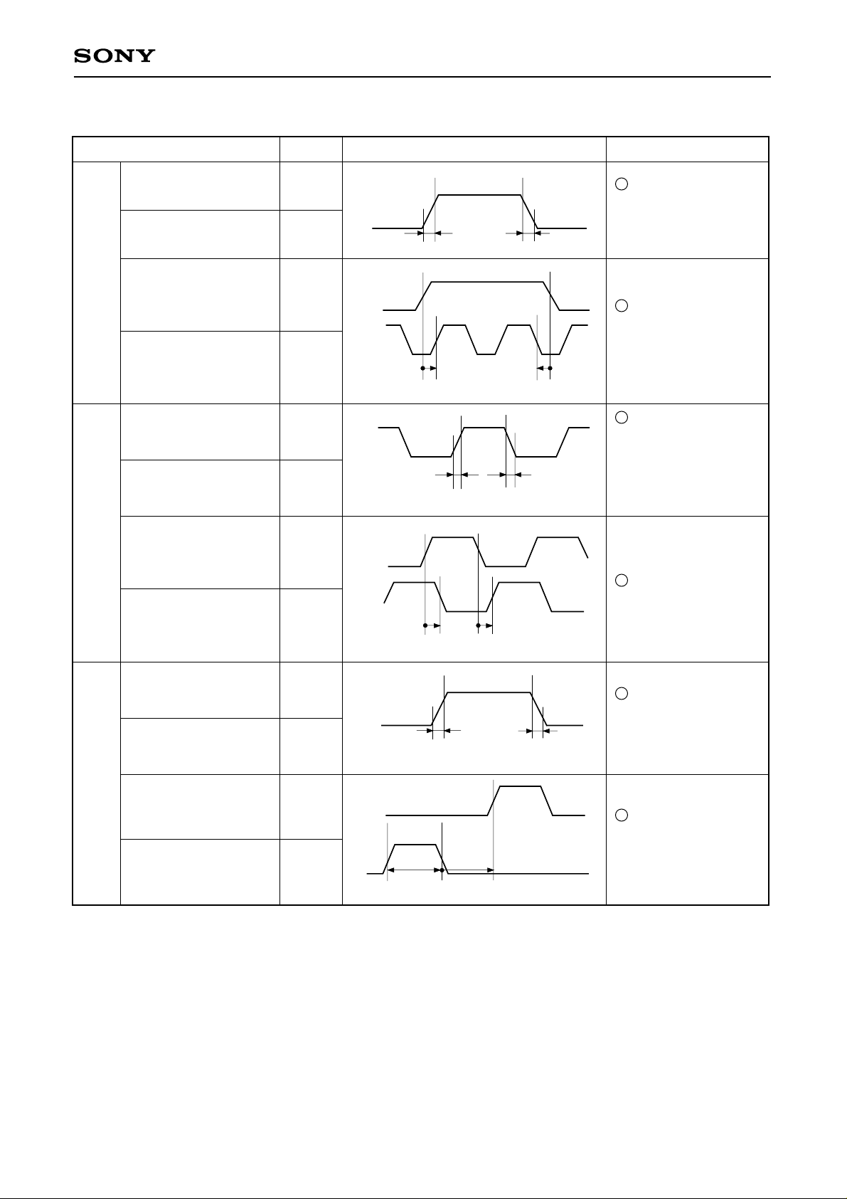
<Horizontal Shift Register Driving Waveform>
Item Symbol Waveform Conditions
LCX005BK
HST
HCK
Hst rise time
Hst fall time
Hst data set-up time
Hst data hold time
Hckn∗2rise time
Hckn∗2fall time
Hck1 fall to Hck2 rise
time
Hck1 rise to Hck2 fall
time
trHst
tfHst
tdHst
thHst
trHckn
tfHckn
to1Hck
to2Hck
HST
∗
3
HST
HCK1
HCKn
∗
3
HCK1
HCK2
90%
10%
trHst tfHst
50%
50%
tdHst thHst
90%
∗
2
10%
trHckn tfHckn
50%
50%
to2Hck to1Hck
90%
50%
50%
50%
90%
10%
10%
50%
∗2
HCKn
duty cycle 50%
to1Hck = 0ns
to2Hck = 0ns
∗2
HCKn
duty cycle 50%
to1Hck = 0ns
to2Hck = 0ns
∗2
HCKn
duty cycle 50%
to1Hck = 0ns
to2Hck = 0ns
tdHst = 135ns
thHst = –135ns
tdHst = 135ns
thHst = –135ns
CLR
Clr rise time
Clr fall time
Clr pulse width
Clr fall to Hst rise time
trClr
tfClr
twClr
toHst
CLR
HST
CLR
90%
10%
trClr tfClr
50%
50% 50%
twClr toHst
90%
10%
∗2
HCKn
duty cycle 50%
to1Hck = 0ns
to2Hck = 0ns
∗2
HCKn
duty cycle 50%
to1Hck = 0ns
to2Hck = 0ns
– 7 –
 Loading...