SONY KV-32HS500, KV-32HV600, KV-34XBR800, KV-36HS500, KV-36XBR800 Training Manual
...
KV-36HV500
Training Manual
KV-57WV700
Direct View/Projection
Television Troubleshooting
DA-4 & DA-4X Chassis
Models: DA-4 DA-4X
KV-32HS500 KP-57WV600
KV-32HV600 KP-57WV700
KV-34XBR800 KP-65WV600
KV-36HS500 KP-65WV700
KV-36XBR800
KV-40XBR800
Theory of Operation & Practical Troubleshooting Tips
Course: C31P15

Table of Contents
1. DA-4 & DA-4X Introduction and
PCB Interconnection ............................1
Introduction............................................................ 1
DA-4 & DA-4X PCD Interconnection................. 1
2. New Features (DA-4 Chassis).........6
Scrolling Index ....................................................... 6
Digital Visual Interface (DVI) ............................... 6
Memory Stick® Interface...................................... 8
3. Power Supply
(DA-4 & DA-4X Chassis).....................12
DA-4 Chassis Power Supply.............................. 12
DA-4X Chassis Power Supply ........................... 20
DA-4 & DA-4X Regulators.................................. 26
4. DA-4 & DA-4X
Protection Circuits ...............................27
5. DA-4 & DA-4X Video Procesing ....45
DA-4 & DA-4X Acceptable Inputs .................... 45
Overall Block Diagram ........................................ 45
6. DA-4 & DA-4X Chassis
Deflection Circuit .................................51
Horizontal Drive Circuit ....................................... 51
DA-4 Vertical Deflection Circuit ......................... 53
DA-4X Horizontal Deflection Circuit .................. 54
DA-4X Vertical Deflectin Circuit......................... 55
7. DA-4 & DA-4X Chassis
Communication Bus Networks ..........56
DA-4 & DA-4X Data Communication
Diagram................................................................ 56
8. DA-4 & DA-4X Audio Circuits ........58
DA-4 & DA-4X Audio Block Diagram.............. 58
DA-4 Protection Circuits ..................................... 27
DA-4X Protection Circuits................................... 37
1. Introduction and DA-4 & DA-4X PCB Interconnection
Chapter 1 - Introduction and
DA-4 & DA-4X PCB Interconnection
Introduction
Overview
The C31P15 course covers the DA-4 (Direct View) and the DA-4X (Projection) chassis. The content includes
new features such as Memory Stick and DVI. Also included is theory of operation and troubleshooting tips for all
major circuits (Power Supplies, Protection, Deflection, Communications and Audio) in the DA-4 and DA-X chassis.
This training manual is based on the KV-32HV600 model.
Objectives
• New Features
• Circuit Theory of Operation
• Component and Board level troubleshooting
DA-4 & DA-4X PCB Interconnection
Overview
The DA-4 (Direct View) and DA-4X (Projection) chassis share many of the same PCBs. The only differences are
found in the RGB Drive, Power Supply and Flash Focus circuits. Table 1-1 indicates the circuits found on each
PCB and if the PCB is board or component level repairable for both the DA-4 and DA-4X chassis.
Table 1-1 DA-4 & DA-4X PCB Circuits and Repair Information
Board Circuits (DA-4) Circuits (DA-4X) Field
Reparability
A
AD
•
A/C
Input
•
STBY 5V
PS
• +9V
Reg.
• +3.3V
Reg.
•
+5V
Reg.
• Main &
Sub.
Tuners
•
Audio
Output
IC’s
•
DYConv.
•
N/A
•
A/C Input
•
STBY 5V
PS
• +9V Reg.
• +3.3V
Reg.
•
+5V Reg.
•
Main &
Sub.
Tuners
• Audio
Output
IC’s
•
Flash
Focus
•
Picture
Centering
•
5V Reg.
Possible
Component
Level Repair
Board Level
Repair
Comments
No DY-Conv.
Circuit for DA4X Chassis
DA-4X chassis
ONLY
1
1. Introduction and DA-4 & DA-4X PCB Interconnection
B
C
D
• H-Protect
•
V-Protect
•
AD-DRC
•
MID-XA
• HD-ADC
• CRT Drive
• A/D DNR
•
Differential
Input
(Memory
Stick®)
• +1.8V Reg.
• +2.5V
Regs.
•
+3V Reg.
•
+3.3V Reg.
•
+5V Reg.
CH (HS) or
CX (HV/XBR)
• RGB Drive
• H & V
Drive
•
H & V DY
•
Main
Power
Supply
+/-15V
+7V
+5V
+11V
+12V
+200V
+33V
Heater
• HV Power
Supply
•
Protection
Circuits
HV Protect
+135
OVP/OCP
HD Protect
IK Protect
• H-Protect
•
V-Protect
•
AD-DRC
•
MID-XA
• HD-ADC
• CRT Drive
• A/D DNR &
SRAM
•
Differential
Input
(Memory
Stick®)
• +1.8V Reg.
• +2.5V Regs.
•
+3V Reg.
•
+3.3V Reg.
•
+5V Reg.
CR, CG, CB
•
RGB Drive
• H & V Drive
•
H & V D
•
HV Drive
•
Convergence
Amps
• +12V Reg.
• +5V Reg.
• +210V
•
+135V
•
Heater
•
Protection
Circuits
HV Protect
HD Drive
+135 OVP/OCP
Board Level
Repair
Possible
Component
Level Repair
Possible
Component
Level Repair
Additional
Circuits on DA4X chassis:
• Extra
VM
circuits
• D-Brd
RGB
connecti
ons
•
SRAM
(IC3001)
Separate RGB
drive boards in
DA-4X chassis
Main Power
Supply located
on D-Brd in DA4 chassis.
Main Power
Supply located
on G-Board in
DA-4X Chassis
2
1. Introduction and DA-4 & DA-4X PCB Interconnection
DH
G
HA
HC
• N/S
Correction
•
E/W
Correction
• N/A
• Key Input
• LED
• Remote
Control
•
Key Input
• LED
• Remote
Control
• N/A
Power Supply
• Unreg. 7V
• Unreg. 5V
•
+/- 15V
•
+/- 19V
•
+135V
•
+33V
• +12V
• +36.5V
• RY6701
•
RY6702
• Key Input
• LED
• Remote
Control
•
N/A
Possible
Component
Level Repair
Possible
Component
Level Repair
Possible
Component
Level Repair
Possible
Component
Level Repair
KV-40XBR800
ONLY
DA-4X chassis
ONLY
All models and
both Da-4 and
DA-4X chassis
Different Part#
for DA-4 & DA 4X
XBR models
ONLY
HB
HM
M
• Front
Video
Input
• Memory
Stick®
• Terminal
Board
• Main
System
Control
•
A/V
Processin
g
• 3D Comb
Filter
• 5V Reg.
• Front
Video
Input
• Memory
Stick®
Terminal
Board
• Main
System
Control
•
A/V
Processin
g
• 3D Comb
Filter
• 5V Reg.
Possible
Component
Level Repair
Board Level
Repair
Board Level
Repair
All models and
both DA-4 and
DA-4X chassis
Different Part#
for DA-4 & DA 4X
All models and
both DA-4 and
DA-4X
chassis’s
Same Part# for
both DA-4 &
DA-4X
All models and
both DA-4 and
DA-4X chassis
Different Part#
for DA-4 & DA 4X
3
1. Introduction and DA-4 & DA-4X PCB Interconnection
MS1
SR
U
UD
VM
W
• Memory
Stick®
Processor
• N/A • Flash
•
A/V
Switch
Terminal
board
•
DVI
Decoder
•
N/A
•
Velocity
Modulatio
n
• Vertical
Pincushio
n
•
N/S
Correction
• Memory
Stick®
Processor
Focus
Sensor
•
A/V
Switch
Terminal
board
•
DVI
Decoder
•
Velocity
Modulatio
n
•
N/A
Board Level
Repair
Board Level
Repair
All models and
Board Level
Repair
Possible
Component
Level Repair
Possible
Component
Level Repair
All models and
both DA -4 and
DA-4X
chassis’s
Different Part#
for DA-4 &
DA-4X
DA-4X chassis
ONLY
both DA -4 and
DA-4X chassis
Same Part#
for both DA -4
& DA -4X
All models and
both DA -4 and
DA-4X chassis
Same Part#
for both DA -4
& DA -4X
DA-4X chassis
ONLY
DA-4 chassis
ONLY
4
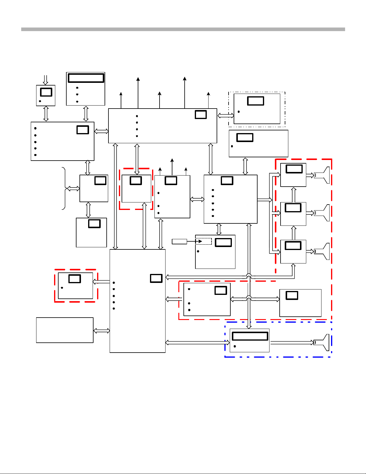
1. Introduction and DA-4 & DA-4X PCB Interconnection
Figure 1-1 illustrates the PCB interconnections for both the DA-4 and DA-4X chassis.
DVI MOLEX
CONNECTOR
UD
DVI
MAIN MICRO
MAIN MICRO
3D COMB
3D COMB
VIDEO PROCESSOR
VIDEO PROCESSOR
AUDIO PROCESSOR
AUDIO PROCESSOR
CCD,V-CHIP,ID1
CCD,V-CHIP,ID1
A/V INPUTS
(1-7)
AUDIO OUT
MONITOR
OUT
S-CONTROL
CHASSIS
HA/HC (XBR)
KEYS
SIRCS
LED
M
A/V
SWITCH
HB
FRONT
A/V INPUT
DA-4X
SPEAKERS
DGC
U
SUPPLY
DA-4X
CHASSIS
CONVERTER
AC/DC POWER
AUDIO POWER
TUNER
DY CONV.,(DA-4)
N/S COIL
G
POWER
ANTENNA
SWITCH
DY
V-PIN COIL
W
VELOCITY
MOD.
V - PIN
N/S DRIVE
MEMORY
STICK
QP COIL
AC
INPUT
A
AD DRC
MID - XA
HD - ADC
CRT DRIVE
AD DNR
HM
MEMORY
STICK
INTERFACE
KV40XBR 800 ONLY
DH
LANDING
CORRECTION
MS 1
MEMORY
STICK PROCESSOR
B
CR
VIDEO
OUT
CG
VIDEO
OUT
CB
VIDEO
OUT
DA-4X
CHASSIS
CRT
CRT
CRT
VM
VELOCITY
MOD
HORIZONTAL &
VERTICAL
DEFLECTION YOKE
FIGURE 1-1 - DA-4 & DA-4X PCB BLOCK INTERCONNECTION DIAGRAM
H/V DRIVE
H/V DY
POWER SUPPLY
AC RECT.
DEFLECTION
D
DIGITAL
REG
PJED CPU
PJE DRIVE
DA-4X
CHASSIS
5
DA-4
CHASSIS
AD
CH/CX(XBR)
VIDEO OUT
SR
FLASH FOCUS
SENSORS
CRT
1C31P15 1478 11/7/02
Chapter 2 - New Features (DA-4 & DA-4X Chassis)
Three new features will be discussed in this section:
• Scrolling Index
• DVI Interface
• Memory Stick® Interface
Scrolling Index
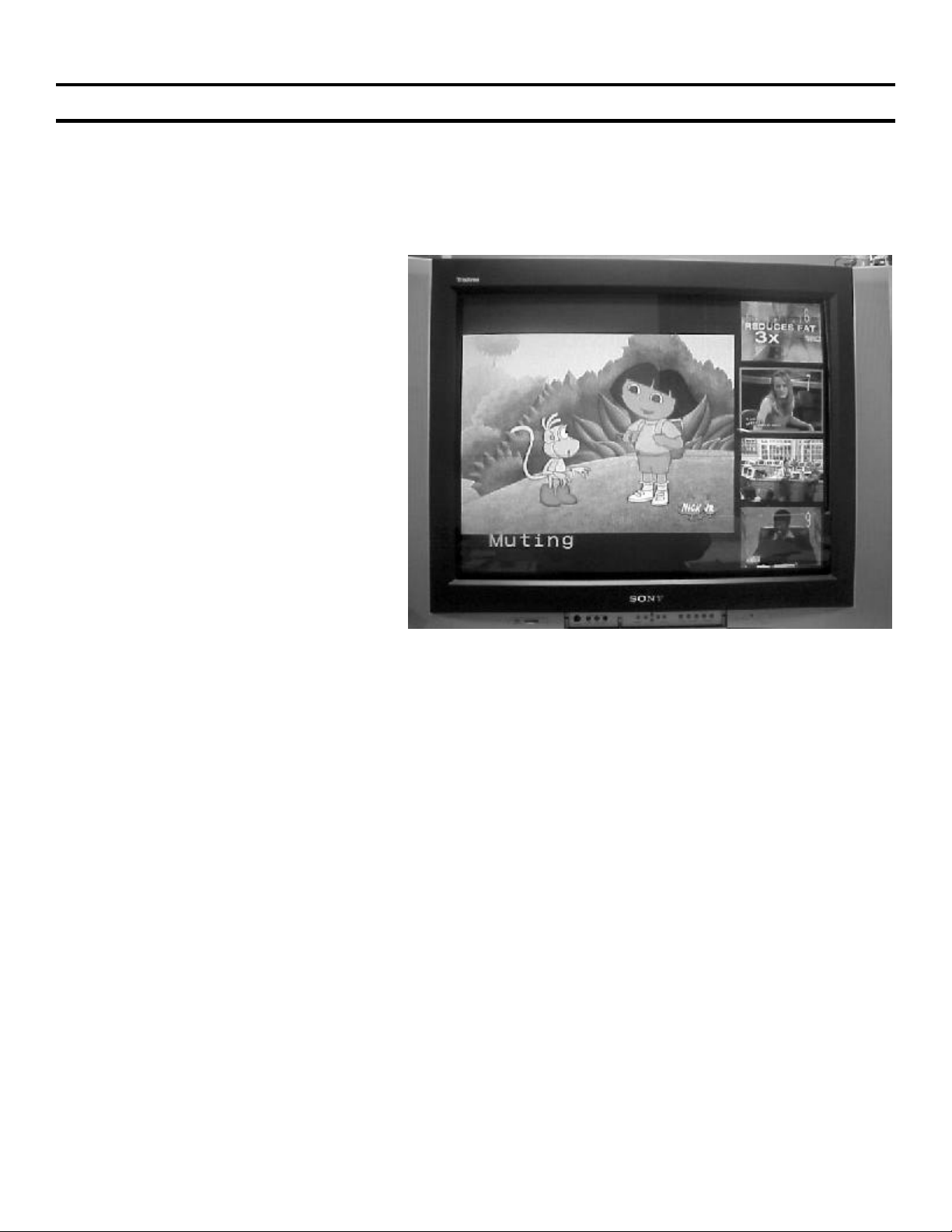
The Scrolling Index allows you to select your
main video from a scrolling index of video
pictures.
The Scrolling Index appears with the currently
selected program in the main (left) window
and four scrolling video pictures in windows
down the right side of the picture tube.
As each picture on the right scrolls to the live
preview window, it changes briefly from a
frozen video to live video. The right side
continues to scroll through the entire channel
list.
2. New Features (DA-4 Chassis)
Factors Affecting the Scrolling Index:
Ø Scrolling Index does not function
if you use a cable box to view all
channels.
Ø Sources connected to the AUX,
Video 5, Video 6 and Video 7 inputs
are visible in the left window, but not in the scrolling right windows.
Ø Scrolling Index does not function if the parental controls are set.
Figure 2-1
Scrolling Index
Digital Visual Interface (DVI)
Introduction
As the digital display technology (e.g. Plasma and LCD) grows so does the need to replace the present analog
HD component connection between external digital device (e.g. Digital TV/Satellite Receiver) and the HDTV
set. The issue is the inherent picture quality problems caused by Digital-to Analog (D/A) and Analog-to-Digital
(A/D) conversion processes.
For example, if you have a digital Plasma display HDTVTM and a Digital TV/Satellite Receiver, the digital video
signal in the Digital TV/Satellite Receiver must be converted to a analog component video signal and then sent
to the HDTVTM where it must be converted back to a digital signal video to drive the Plasma display. Because of
the two video signals conversion steps and the possible analog signal loss across the connection between the
HDTVTM and the Digital TV/Satellite Receiver, the picture quality will suffer. Even with an analog CRT the Digital
TV/Satellite Receiver video signal must go through D/A conversion, which can adversely affect picture quality.
TM
The resolution to this dilemma is the creation of a complete end-to-end standard digital video interface, such as
DVI. The DVI interface is a high-speed digital video interface allowing uncompressed high-definition content to
be passed to another DVI equipped device such as an HDTVTM set. DVI is the only digital interface capable of
6
2. New Features (DA-4 Chassis)
accommodating uncompressed digital data such as HD video. DVI also has the bandwidth to support higher
audio fidelity.
DVI has a bandwidth of up to 5 Gigabits/sec, which is more then enough to accommodate an uncompressed HD
video transmission that typically requires 2.2 Gigabits/sec bandwidth.
DVI Connector and Decoding Block
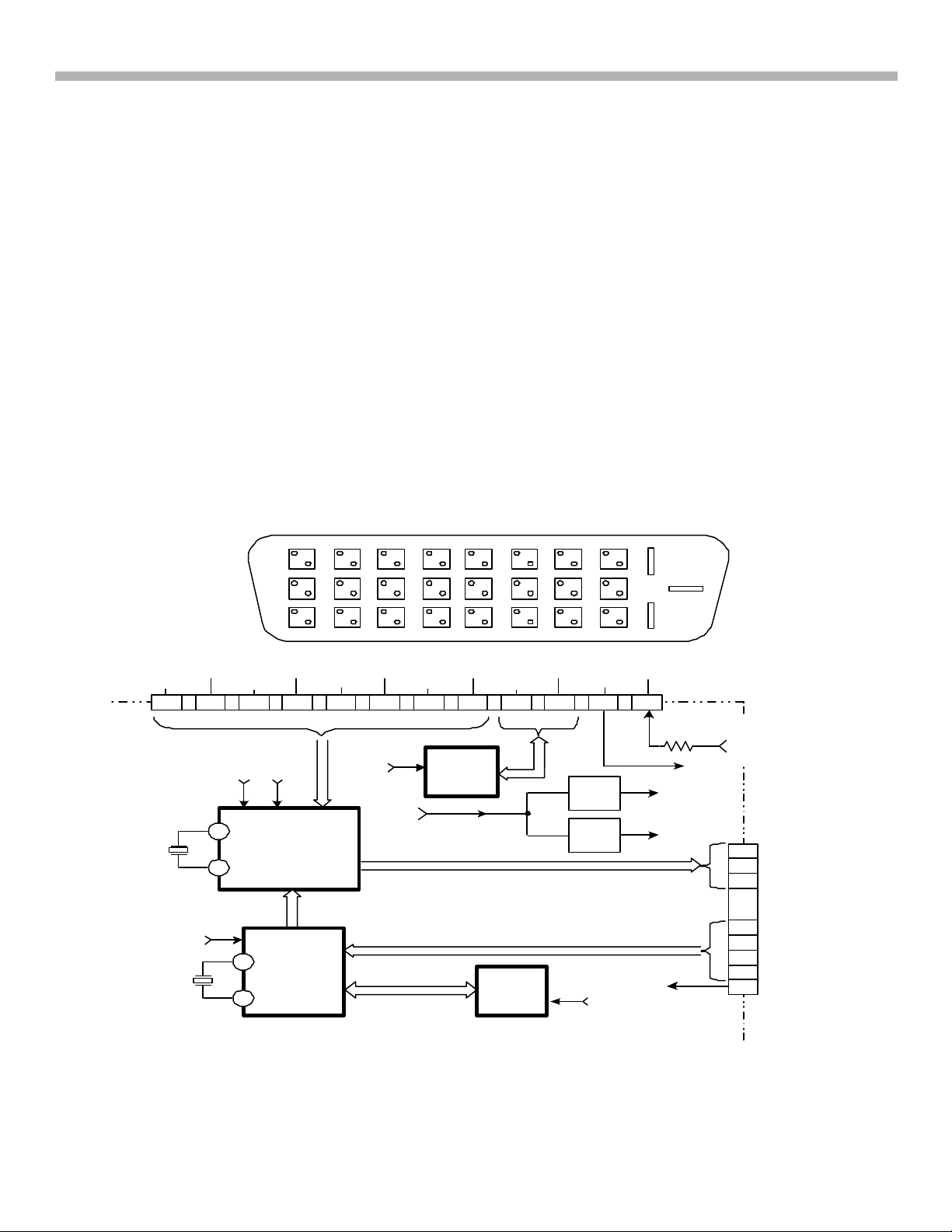
The DVI Molex connector and Decoding circuitry for both the DA-4 and DA-4X chassis are located on the UDBoard (NOTE: This board is NOT field repairable). Figure 2-2 shows a block diagram for the UD-Board. The
DVI signal (from a Digital TV/Satellite Receiver) is received at the 24-pin Molex connector CN7001. There are
three serial data differential channels RX0+/RX0-, RX1+/RX1-, RX2+/RX2- and one reference clock differential
channel RXC+/RXC-.
IC7001 NVM is also connected to the external device through the SDA and SCL (I2C) bus. IC7001 stores the
EDID data (Extended Display Identification Data) and HDCP (High Definition Digital Content Protection).
EDID is sent to inform the external digital device of the TV’s identity and capabilities.
HDCP is an Authentication protocol between the external digital device (transmitter) and the TV (receiver) that
affirms to the transmitter that the receiver is authorized to receive the protected information.
CN 7001/pin 14 (5V) is supplied from the external digital device to power IC7001 (NVM) so EDID can be sent
when the TV set is OFF. If the TV set is ON, IC7001 will receiver 5V from CN7002 through D7001.
CN7001/pin 16 is the Hot Plug Detect pin (HPD). The TV set supplies 5V to the external digital device to verify
proper connection between the two devices.
CONNECTOR
R x 2+
R x 2-
1 2 9
X7001
14.31818MHz
5V
X7002
12MHz
R x 1+
R x 1-
3.3V
2.5V
94
95
IC7004
DVI-DECODER
2
IC7005
MCU
3
R x 0-
10 17
SDA,
SCL
R x C+
IC7001
R x C-
NVM
SCL
IC7006
NVM
R x 0+
18 23 24 6 7
5V
5V
SDA, SCL
SDA
5V
14
3.3V
REG
2.5V
REG
5V
HPD
16
5V
CN7001
24P MOLEX
CONNECTOR
R7021
10kHz
3.3V
2.5V
5V TO
D7001
CN2304/
PIN 1
5V
10
8
6
13
4
3
2
1
CN7002
Y
PB
PR
SET-UP
MUTE
VGA
RESET
5V
FIGURE 2-2 - UD - BOARD BLOCK (DVI DECODER)
C31P15-2-2 1501 10/31/02
The DVI Decoder, IC7004 receives the three channels of digital video data and outputs analog component video
(Y, PB, PR) to CN7002/pins 10, 8 and 6 respectively.
7
2. New Features (DA-4 Chassis)
Memory Stick® Interface
Introduction
Memory Stick® is a new compact, portable and versatile Integrated Circuit Recording Medium with a data
capacity that exceeds that of a floppy disk. The internal memory circuit structure is a type of Flash Memory
similar to that found in a personal computer. It is a solid-state design, which basically means there are no moving
parts. Inside the Memory Stick® is a grid of columns and rows with a two-transistor cell at each intersection point
on the gird, which is used to store a 1 or 0. The Memory Stick® is specially designed for the exchange and
sharing of digital data among Memory Stick® compatible products such as Digital Still Cameras and Digital Video
Cameras. Because it is removable, Memory Stick® can also be used for external data storage.
Memory Stick® technology allows you to view on the TV digital (JPEG) still images that are stored on Memory
Stick® medium. You can choose from an index of the images stored on the Memory Stick® or you can run a
slideshow of those images.
The DA-4 and DA-4X chassis Memory Stick® viewer can display ONLY Still Images that have been recorded on
Memory Stick® media by Sony brand digital still and video cameras.
Recorded images must meet the following specifications:
Ø Compression format: JPEG
Ø File format: DCF compliant
NOTE: Most Sony brand digital still and video cameras automatically record still images using DCF
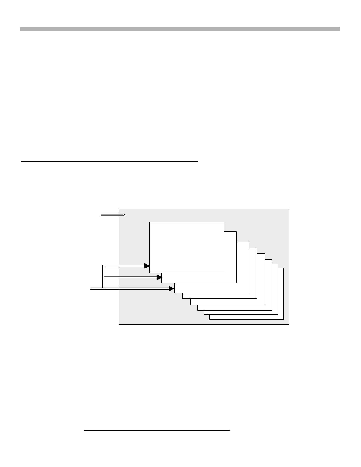
(Design rule for Camera File system) compliant directory and file names as shown in Figure 2-3:
IMAGE
DIRECTORY
NAME
IMAGE FILE
NAMES
NOTE:
DO NOT RENAME DIRECTORIES.
IF THE NAMES ARE CHANGED,
THE STILL IMAGES CANNOT BE
DISPLAYED ON YOUR TV.
100MSDCF
DSC0001
DSC0002
DSC0003
FIGURE 2-3 - DCF DIRECTORY
C31P15-2-3 1504 9/26/02
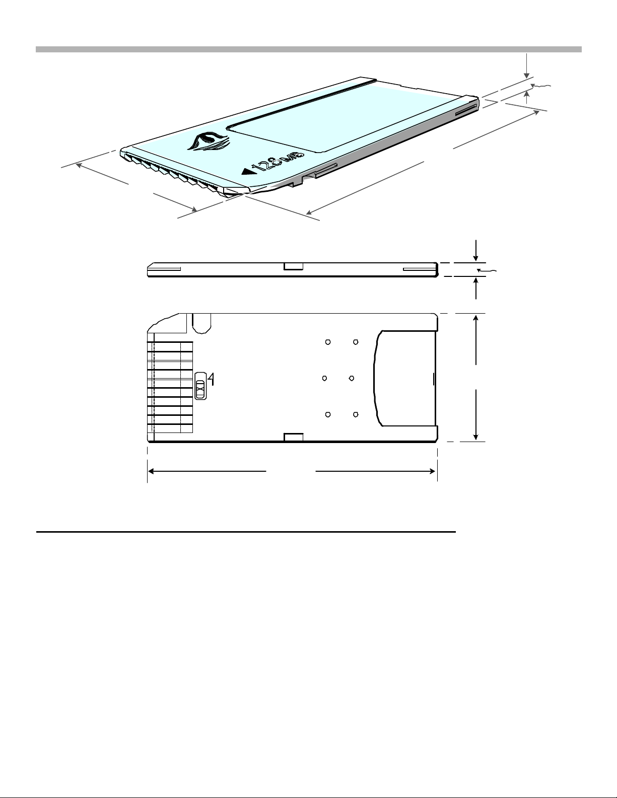
The main advantage of the Memory Stick® is its size, which measures approximately 2’’x3/4"x1/8", making it
extremely portable (reference Figure 2-3). However, do not let the size fool you; the Memory Stick® comes in
five data capacity ratings: 8MB, 16MB, 32MB, 64MB, 128MB and 256MB.
Note: The DA-4 and DA-4X chassis Memory Stick® viewer is compatible with Memory Sticks® up to and
including 128MB. **The 256MB Memory Stick® is not compatible.**
8
2. New Features (DA-4 Chassis)
TOP VIEW
VIEW OF
LOWER
SIDE
MEMORY STICK
7/8"
1/8"
2"
1/8"
7/8"
LOCK
2"
FIGURE 2-4 - MEMORY STICK DIMENSIONS
C31P15-2-4 1505 9/16/02
The DA-4 and DA-4X Memory Stick® viewer cannot display any of the following:
Ø Images recorded on digital still cameras and digital video cameras that are not Sony brand.
Ø Images recorded using products that are not DCF complaint, including the following Sony products:
• Digital still cameras DSC-D700
DSC-D770
• Digital video cameras DCR-TRV900
DSR-PD100A
Ø Images stored on a Memory Stick® that has a capacity that exceeds 128MB.
Ø Images stored in TIFF or any other non-JPEG compression format.
Ø Images in directories that were modified or renamed on a computer.
Ø Images with less than 16 horizontal and/or vertical dots per line.
Ø Images with more than 4096 horizontal and/or vertical dots per line.
9
Memory Stick Interface and Processing Block
MEMORY
STICK
CN7201
HM BOARD
2. New Features (DA-4 Chassis)
MS-BS+
3.3V
3
5 6 7 8 9 10
B3 A4 BY A5
MS-DIR+
MS-BS-
DIFF. - AMPS
& BUFFER
MS-SCLK-MS-DIR-
A6 B6 A7 B7
B5
B BOARD
MS1 BOARD
MS-SDO+MS-SCLK+
11
MS-SDI+ MS-INS
MS-SDO-
12 13
A8
MID
MS-SDI
14
B8 B9
15
CN7202
CN3603
TO CRT
DRIVE
CN3601
CN104
MS DECODER BOARD
FIGURE 2-5 - MEMORY STICK INTERFACE & PROCESSING BLOCK
C31P15-2-5 1502 11/7/02
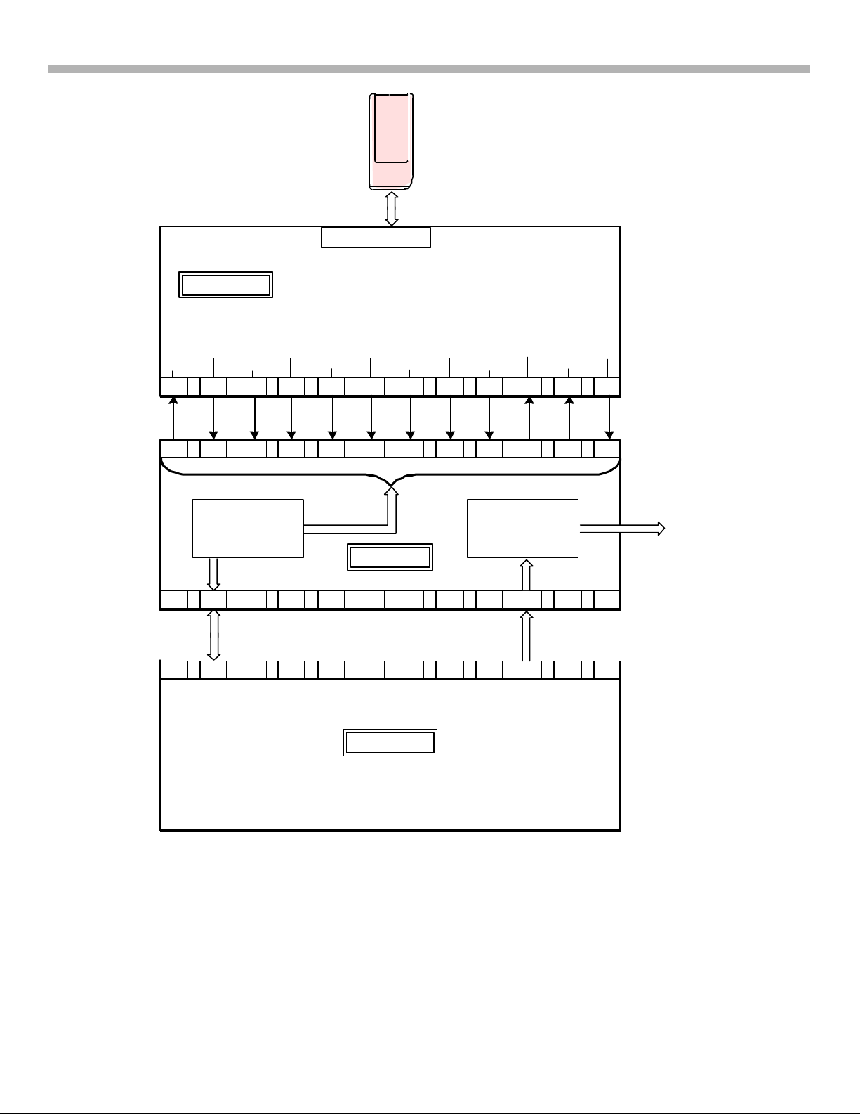
The Memory Stick® (MS) is inserted into CN7201 on the HM-Board. Once the MS is completely seated
in the slot, the Memory Stick® applies a ground to CN7202/pin 15 (MS-INS), which goes Low (from
3.3V to 0V). This notifies the MS1-Board that a MS has been inserted. Initial data will be transferred at
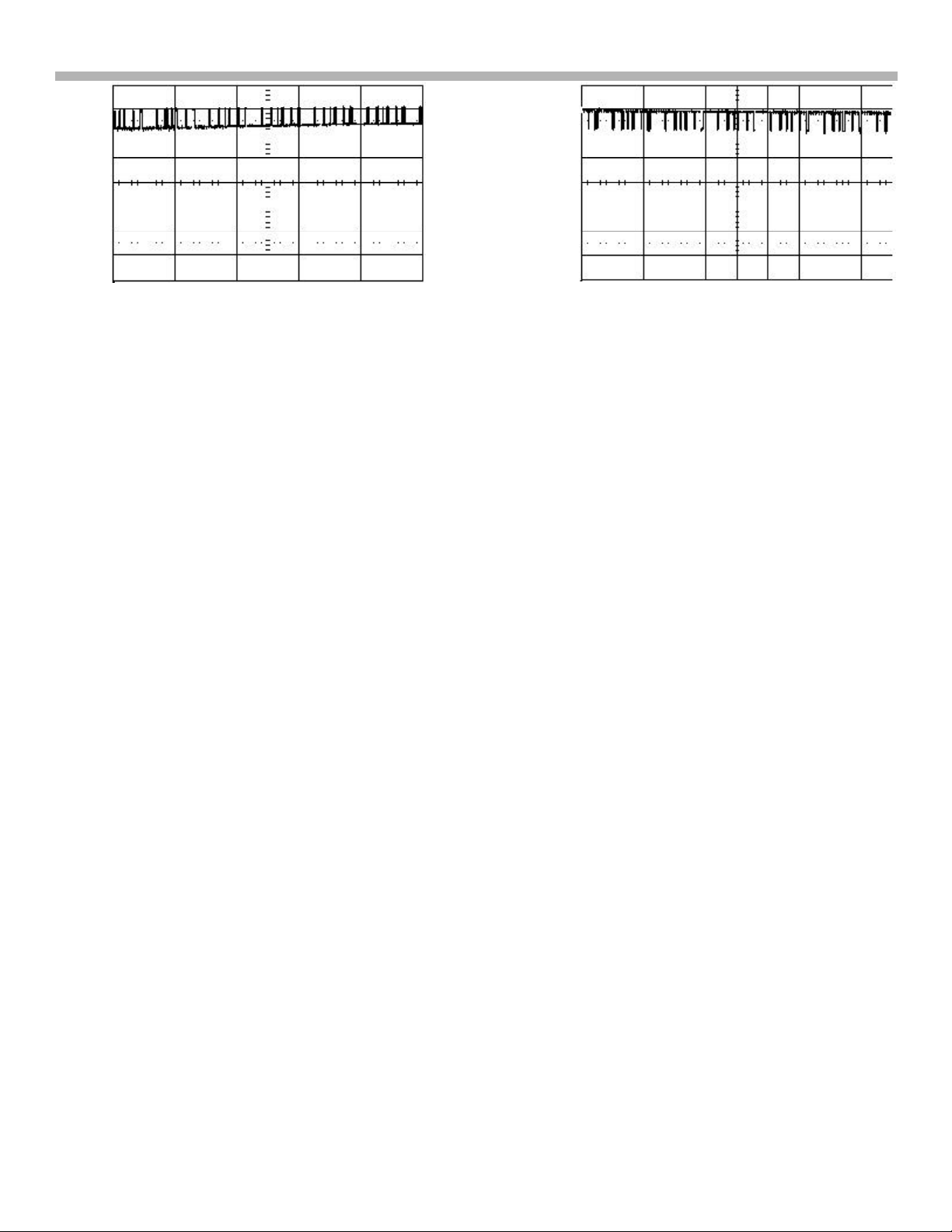
this time between the HM-Board and MS1-Board and can be viewed at CN7202/pins 5 through 14
(reference Waveforms 2-1 and 2-2). The data signals are all in differential format with a positive and
negative signal. The differential format is incorporated to eliminate noise on the data lines. Data can be
viewed on these pins when the MS is initially inserted and when an image is selected for display on the
CRT.
10
2. New Features (DA-4 Chassis)
CH2
.5v
100us
Waveform 2-1
MS - SDI (+)
CH2
.5v
100us
Waveform 2-2
MS - SDI (-)
The MS-INS is applied to the B Board/pin B3 and forwarded on to the MS1- Board. The MS-Data
signals are amplified on the HM-Board and then applied to the B Board/pins A4/B4 through A8/B8
where they are converted from differential format to single data lines, and further amplified and applied
to the MS1-Board.
The MS1 Board performs the following functions:
• Memory Stick® System Control
• JPEG Processing
• Memory Stick Decoding
The Memory Stick® JPEG data is then converted into digital Y, CB, CR data on the MS1 Board. The
digital Y, CB, CR data is then sent back to the B Board and is D/A converted to analog component video
signals (Y, CB and CR), which drive the CRT.
Troubleshooting Tips
1) All three boards (HM, Band MS1) are Not Field Repairable .
2) Confirm CN7202/pin 15 (MS-INS) goes low when Memory Stick® is inserted.
3) Confirm CN7202/pin 3 (3.3V supply).
4) Confirm CN7202/pins 5 through 14 have data activity during the following two events:
a. When the Memory Stick® is initially inserted; and
b. When an image is selected for display on the CRT.
5) Confirm the voltages and signals in steps 2, 3 and 4 are applied to CN3603/pins B3, A4/B4
through A8/B8 and B9.
6) If all voltages and signals are applied to the B Board, further troubleshooting will be board swap
due to inaccessibility to connectors on the B Board and MS1 Board.
There is not much signal processing performed on the B Board, so the most likely defect at this point
would be the MS1 Board.
11
3. Power Supply (DA-4 & DA-4X Chassis)
Chapter 3 - Power Supply (DA-4 & DA-4X Chassis)
This chapter will cover the power supply section for both the DA-4 and DA-4X chassis. The degauss circuit for
the DA-4 chassis will also be discussed.
The power supplies for the DA-4 and DA-4X chassis are almost identical except in the following two main areas:
1) High Voltage (HV) development: The HV on the DA-4 chassis is Switch-mode power supply derived, whereas
the HV on the DA-4X chassis is scan derived.
2) Circuit Location: On the DA-4 chassis, the power supply circuitry is located on the A and D-boards, whereas
on the DA-4X chassis, the circuitry is on the A, D and G boards.
Except for the development of the HV, the circuit operation for the Standby 5V and Main Converter Power
Supplies is identical. Notes and references are placed on each diagram where the circuit operation is
identical between the two chassis. The circuit itself may be located on a different board and component
reference numbers may be different, but the components are the same. As you read this section, note the
similarities and differences between the DA-4 and DA-4X chassis.
DA-4 Chassis Power Supply
DA-4 Overall Power Supply Block
VD501
AC
T510 T511
STANDBY 5V
POWER
SUPPLY
STANDBY
5V CIRCUIT
HA/HE BD.
M BD.
A BOARD
D BOARD
FH501
GND.FROM
Q6527
(AC
RELAY)
FROM D508,D509
(INRUSH
RELAY)
UNREG
RY6501
R6516
RY6502
FROM
11V
1 2
CN514
CN6502
TH501
RY501
DGC
IC6501
MAIN
POWER
SUPPLY
AC-RECT
IC8002
HV POWER
SUPPLY
13V FROM 5V STBY
D501
Q502
FROM AC RECT.
BLOCK D6530
T8001
FBT
D503/C506
+
C507
36.5V
+/- 15V
UNREG 7V
UNREG 5V
UNREG 11V
+135V
+200V
R506
HV
G2
FV
ABL
DF
Q501
DGC-ON
FROM
IC2300
/PIN 68
( M-BD.)
H-OUT
Q5030
FIGURE 3-1 - DA-4 POWER SUPPLY OVERALL BLOCK
HOT
T5001
IC5006
12
H1( HEATER)
C31P15-3-1 1509 10/28/02

3. Power Supply (DA-4 & DA-4X Chassis)
DA-4 Overall Power Supply Block Description
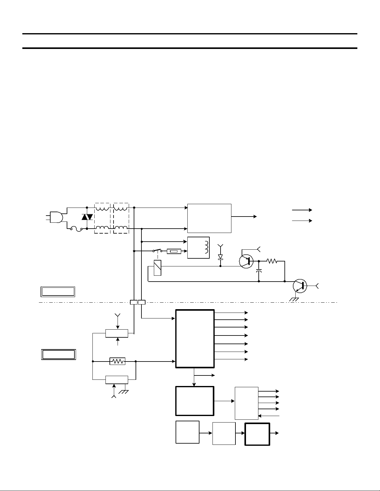
Once 120V AC power is applied to the TV set (set plugged into the AC outlet), the Standby 5V power supply
(located on the A-board) is active and outputs regulated 5V (reference Figure 3-1). The STBY 5V is sent to the
M-board to partially power-up system control IC2300 and is also sent to the HA/HC board to power the Remote
Control Sensor (SIRCS).
The Main Converter power supply (DA-4) located on the D-board is fed AC (from A-Board) through the AC-
Relay (RY6501) and through Inrush-Current resistor (R6516). This limits the initial high current produced when
the TV set is first turned ON. The Inrush-Current resistor (R6516) is removed from the AC input path using
RY6501. Once the Main Converter power is up and running, the unreg11V output is fed back to RY6501, the
relay switch is closed and R6516 is bypassed in normal operation. The Main Converter power supply outputs the
following voltages:
• +/- 15V
• Unreg7V
• Unreg5V
• Unreg11V
• 36.5V
• +135
• +200
The High Voltage (HV) on the DA-4 chassis is developed using a switch-mode power supply identical to the one
found in the Main Converter power supply except for the use of the Flyback (FB) T8001 as the output transformer
(reference Figure 3-1). The HV power supply is located on the D-board. The HV power supply is activated
simultaneously with the Main Converter power supply. AC power is fed to the HV power supply from the ACRECT block (D6530), which also feeds the Main Converter power supply. The HV Converter output then drives
the FB transformer, which outputs the following voltages:
• High Voltage (HV)
• Focus Voltage (FV)
• G2
• ABL
The Heater Voltage is scan derived using H-Out (Q5030), T5001 and IC5006 also located on the D-board.
The Degauss Circuit (reference Figure 3-1) will be activated after IC2300 (M-board) receives an ON command
from either the ON/OFF button or the remote control, and after one of the following events have occurred:
• The AC power was disconnected (indicating that the TV was possibly relocated).
• The TV has been turned OFF for more then 15 minutes.
The base of Q501 receives a high from IC2300/pin 68 (turning Q501 ON). The ground path for the degauss relay
RY501 and the base circuit of Q502 are completed through the collector/emitter circuit of Q501. Q502 supplies
the initial kick voltage and current to RY501. Once C504 in the base circuit charges completely, Q502 will turn off
and a hold voltage is supplied through D501 (13V) from the STBY Power Supply circuit.
RY501 switch closes and sends AC through the degauss coil, eliminating any magnetic fields present in the
metallic parts in the picture tube, which could cause color purity problems. The degauss relay remains closed for
approximately six seconds and then opens.
13
3. Power Supply (DA-4 & DA-4X Chassis)
Three relay clicks will be heard when the set is first turned on in the following order:
1) Degauss Relay (RY501)
2) AC Relay (RY6501)
3) Inrush Current Relay (RY6502)
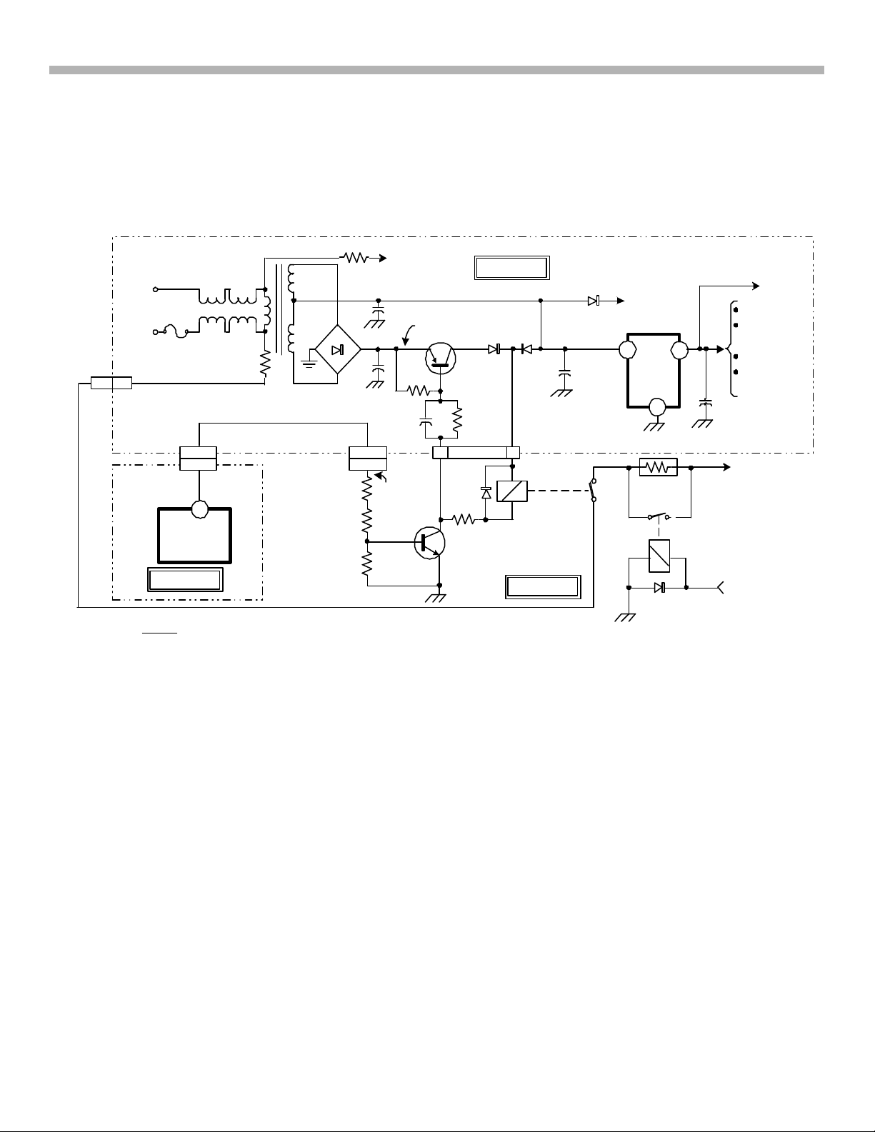
DA-4 STBY 5V Power Supply and Power-On Switching Circuit
CN6502
T502
L511
L510
AC
INPUT
FH501
CN514
22
CN523
CN2002
IC2300
M BOARD
NOTE
CIRCUIT OPERATION IS THE SAME FOR BOTH DA-4 & DA-4X CHASSIS
R509
19
19
69
D503
R510
C507
C506
CN900
CN5011
R6528
R6509
R6530
TO D-BOARD
AC TO D6530
+
+
R513
C513
7
7
ON 0.6V
STBY-0V
CN6701
ON 20V
STBY 23V
+
8
A BOARD
D508
Q503
R516
D6534
R6519
Q6527
D509
ON-8.5V
STBY-22V
CN521
5
CN6506
AC RELAY
RY6501
D BOARD
D501
ON 9V
STBY 11V
+
C514
(AC)
TO RY501
DEGAUSS
RELAY
SOLENOID
I
IC501
STBY
5V
G
R6516
D6533
BD.
O
5V
+
RY6502
(INRUSH)
RELAY
HA/HC
BD.
Q2312
M
IC2300
SYSCON
IC2302 NVM
IC2305 3.3V
REG
C515
TO D6530
MAIN POWER
SUPPLY
UNREG 11V
OUTPUT FROM
MAIN POWER
SUPPLY
FIGURE 3-2 - DA-4 STANDBY 5V POWER SUPPLY & POWER ON SWITCHING CIRCUIT
C31P15-3-2 1508 11/12/02
Standby 5V Power Supply
Reference Figure 3-2 during the following circuit description:
The Standby Power Supply (located on the A-board) is operational as long as the set is plugged into an AC outlet.
AC power is applied to T502 through fuse FH501 and chokes L510 and L511. T502 couples the AC across to
D503 rectifier block and filter capacitor C507 (AC is also coupled to Q503; this is part of the power-on switching
circuit which will be discussed next).
The Standby 5V power supply is a simple conventional full-wave (only two diodes in D503 are used) rectifier
circuit. The resulting DC voltage (11V) is applied to the input pin of IC501 (5V regulator), which then supplies
regulated 5V to the following components:
• IC2300 System Control (M-board)
• IC2302 NVM (M-board)
• IC2305 3.3V Regulator (M-board)
• Q2312 Remote Input Buffer
• HA/HC boards (Key Input, LED and Remote Sensor)
14

3. Power Supply (DA-4 & DA-4X Chassis)
Power-ON Switching Circuit
Reference Figure 3-2 during the following circuit description:
In the Standby mode, System Control (IC2300) is partially powered (using STBY 5V) and waiting for an ON
command from either the Front Panel Controls (IC2300/pins 93 and 94) or the Remote Control (IC2300/pin 7).
Once the ON command is received, IC2300/pin 69 (AC_RLY) outputs a high, which is applied to the base of
Q6527 (turning Q6527 ON). This completes the ground path for the AC Relay (RY6501) and for the base circuit
of Q503.
Q503 turns on and supplies the initial kick voltage and current through D508 to RY6501, closing the relay switch
and supplying AC power to the Main Power Supply through Inrush resistor R6516 and D6530. Once C513 in the
base circuit charges completely Q503 turns off; D508 reverse biases and D509 forward biases, supplying a hold
voltage (9V) to keep the relay switch closed in the ON mode.
At this point the Main Power supply is turning ON (operation will be discussed next). The initial AC power to the
Main Power Supply is through Inrush resistor R6516, which limits the high surge current that occurs momentarily
at turn ON. Once the secondary voltage UNREG 11V is developed on T6502 in the Main Power Supply, it is fed
back to the Inrush Relay (RY6502). RY6502 turns on and bypasses R6516 in the ON mode. R6516 is only in
the circuit during initial power-up of the set.
Troubleshooting Tip:
Obviously, if a failure occurs in the 5V Standby Power Supply the unit will not even attempt to turn ON. If this
condition occurs, check the following components:
1) FH501
2) 13V at IC501 Input Pin (I). If missing, suspect T502, D503 and/or C507.
3) 5V at IC501 Output Pin (O). If missing, suspect a defective IC501.
4) NOTE: Q503 is used as a current source for the AC relay (RY6501). If the collector/emitter junction of
Q503 becomes an Open circuit, the set will still turn ON (using voltage through D509) and function
properly with sufficient AC power input. If the AC power input is weak (Low Voltage ~90VAC, the unit will
have difficulty turning ON without Q503 functioning properly.
15
DA-4 Main Switching Power Supply Circuit
3. Power Supply (DA-4 & DA-4X Chassis)
CN6701
CN514
1
1
D6530
AC RECT.
FROM
RY6501
R6646
R6514
R6513
R6517
D6502
+
C6508
+
C6519
D-BOARD
NOTE:
CIRCUIT OPERATION
IS THE SAME FOR
BOTH DA4 & DA4X
CHASSIS'
A-BOARD
TO IC8002/PIN 1
HV POWER SUPPLY
R6526
FILTER
CIRCUIT
V-SENSE
2.7V
1
IC6501
MCZ
3001D
14
VB
10.6V
10
VC2
6
TIMER
F/B
2 8
1.9V
TO IC8002/
R6525
VG
(H)
VS
VG
(L)
OCP
VCI
+
PIN 8
R6536
279V
18
141V
16
15
12
4.8V
9
18V
C6558
R6524
5
136V
Q6506
0V
D6519
D6520
+
C6549
4 1
3 2
TO A BD.
AUDIO VCC
(36.5V)
2
4
C6546
+
D6514
Q6507
275Vp-p
78kHz
C6352R6557
R6556
R6501
R6505
R6508
R6510
PH6502
1
CN6503
L6516
R6544
11V
1
2
6
7
8
9
+15V
R6503
T6502
18
17
16
15
14
13
2.4V
C6551
D6513
PS6506
PS6505
D6504
D6524
11
C6556
10
D6518
IC6503
4 1
DM-58
CONT.
3
+
5
R6539
+
C6557
133V
+
D6516
+
D6523
+
+
L6505
L6501
R6590
UNREG
7V
UNREG
5V
UNREG
11V
+15V
C6597
C6559
-15V
+33V
C6502
D6508
33V
+135V
+200V
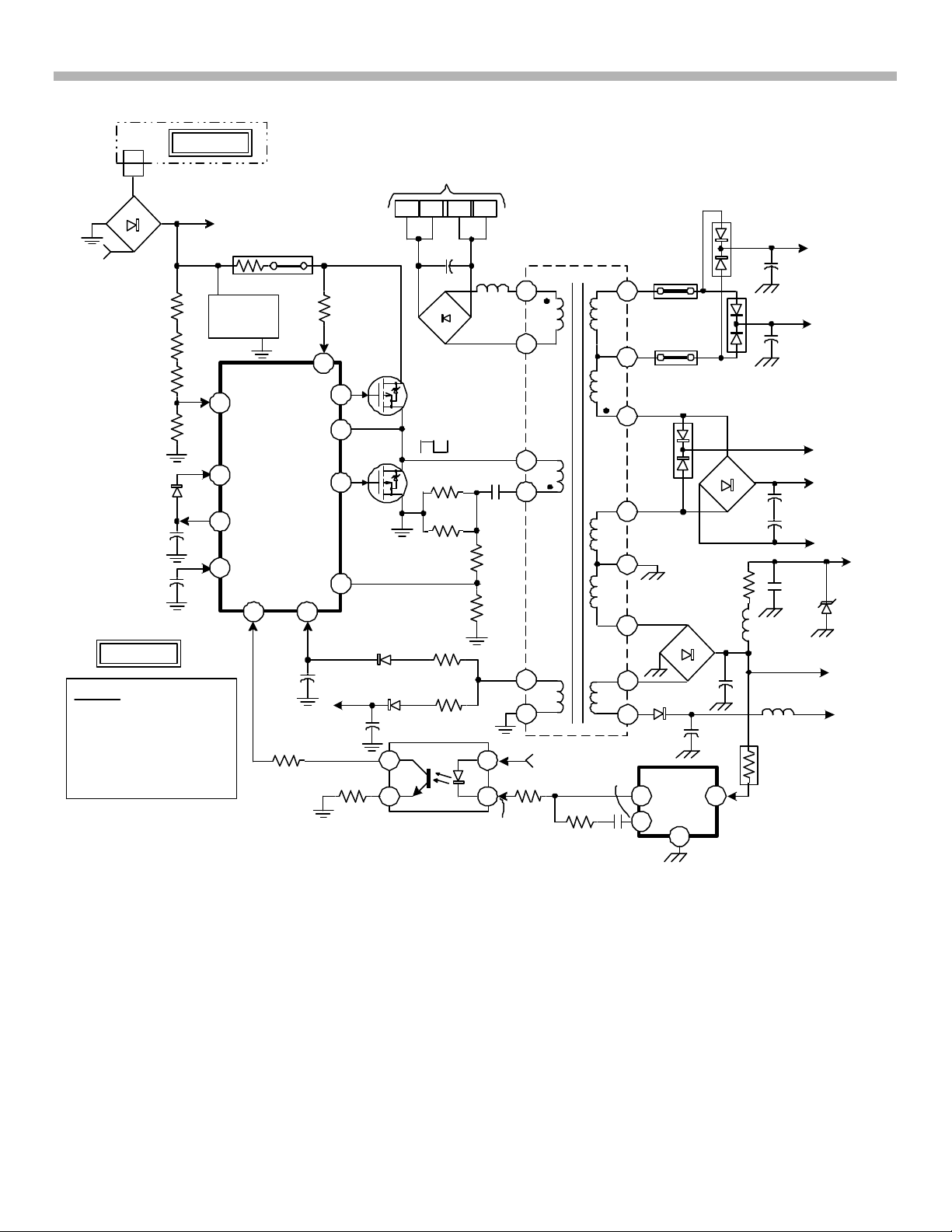
FIGURE 3-3- DA-4 MAIN POWER SUPPLY CIRCUIT
C31P15-3-3 1506 11/8/02
The Main Switching Power supply is basically IC6501 (Switch Regulator Controller). IC6501 contains all the
major circuitry necessary to function as a switching power supply, except for the Power Switching MOSFETS
(Q6507 and Q6506).
IC6501 contains:
• Control circuit
• Oscillator/Oscillator control
• Output Driver transistors
• 10V regulator
• Shut-Off Timer
• Over Current Protection
16

3. Power Supply (DA-4 & DA-4X Chassis)
Main Switching Power Supply Operation
Reference Figure 3-3 for the following circuit description:
AC signal is applied to the rectifier block D6530. The AC component is filtered-out by the filter circuit (shown in
block form). A DC voltage of 293V is produced at the output of the filter circuit.
IC6501 Startup Sequence
1) Turn ON voltage: The 293Vdc from the filter circuit is voltage divided by R6646, R6514, R6513 and
R6517 down to 2.7Vdc. This voltage is applied to IC6501/pin 1 (Vsense) and IC6501 turns ON. IC6501/
pin1 (Vsense) is also used for OVP protection (IC6501/pin 1 > 8V will trigger OVP).
2) Internal circuit Start Voltage: The 293Vdc also passes through voltage dropping resistors R6526 and
R6536, and 279Vdc is applied to IC6501/pin 18. This voltage is used to initially power the internal circuits
and begin oscillations. Note that the 293Vdc from R6526 is connected directly to the Drain of Q6507 and
serves as the High-side FET power source.
Internal circuits initially powered by IC6501/pin 18
• Internal drive transistors for High-side output FET Q6507.
• Oscillator
• Control circuit
• 10V regulator (IC6501/pin 10)
Note: The 10V output at IC6501/pin 10 passes through D6502 and supplies power to the internal
driver transistor for the Low-side output FET Q6506
3) Output Oscillations: At this point, initial square-wave oscillations of approximately 125KHz are output at
IC6501/ pins 16 and 12. Normal operation frequency is approximately 85KHz.
4) Regulator Feedback: The feedback line is connected to the +135V secondary output. Once IC6501 is
turned ON and oscillations begin, the secondary winding at T6502/pin 13 and associated circuitry produces
+135V. The +135V is applied to IC6503/pin 1 (DM-58 Control).
IC6503 controls the voltage at the PH6502/pin 2, which controls the current output of the optic-coupler
PH6502. The amount of current supplied to IC6501/pin 2 depends on how hard PH6502 is turned ON. In
normal operation, a voltage of 1.9Vdc (which is proportional to the amount of current) is present at
IC6501/pin 2. The feedback loop is now complete.
5) IC6501 normal operating power supply (VC1): Produced simultaneously with the oscillator feedback is
the operating power source VC1.
IC6501/pin 8 (VC1) is produced using a winding on T6502/pin 8. The AC is rectified and filtered, and a
DC voltage of 18V is applied to IC6501/pin 8. Once the 24V is stable, IC6501’s internal control circuit
disconnects (internally) the power source at IC6501/pin 18. All IC6501 internal circuits are now powered
from IC6501/pin 8.
Over Current Protection (OCP): ref. Figure 3-3
The current flowing through the switching FETS (Q6507 & Q6506) also passes through T6502/pins 6 and 7,
C6532 and resistor bank R6557 and R6556. The voltage drop across resistor bank R6557 and R6556 is
directly proportional to the current through the switching FETS. The voltage across R6557 and R6556 is
further voltage divided by R6501 and R6505 and applied to IC6501/pin 9. The OCP is activated when the
voltage at IC6501/pin 9 exceeds 0.2V. The self-diagnostic indicator will flash four times, pause and then
repeat.
17
 Loading...