

Sony KP-XR432K90, KP-XR432N90 Service manual
SERVICE MANUAL
RA-3A
CHASSIS
MODEL COMMANDER DEST. CHASSIS NO.
–––––– –––––––––––– ––––– –––––––––––
KP-XR432K90 RM-Y906KKorean SCC-P50D-A
KP-XR432N90 RM-Y906 Taiwan SCC-P50C-A
MODEL COMMANDER DEST. CHASSIS NO.
–––––– –––––––––––– ––––– –––––––––––
DVD/
POWER
MUTING
SAT/
VTR
CABLE
TV
FUNCTION
SYSTEM
OFF
DVD/VTR SAT/CABLE
TV
TV/VTR
FREEZE
SWAP PIP
m
N
M
AUDIO
POSITION ACTIVE
X
xz
ANT
TV/VIDEO
SLEEP
PICTURE
CC
MODE
DISPLAYMTS/SAP
2
1
3
5
6
4
8
7
9
JUMP
ENTER
0
INDEX
GUIDE
RESET
MENU
VOL CH
CODE SET
TV
RM-Y906/Y906K
KP-XR432K90/432N90
PROJECTION TV

SPECIFICATIONS
KP-XR432K90/XR432N90
RM-Y906K RM-Y906
Projection system
3 picture tubes, 3 lenses, horizontal in-line
system
Picture tube
7-inch high-brightness monochrome tubes (6.3 raster size),
with optical coupling and liquid cooling system
Projection lenses
High performance, large diameter hybrid lens F1.05
Television system
American TV standard
Channel coverage
VHF: 2–13/UHF: 14 –69/CATV: 1 – 125
Antenna
75 ohm external terminal for VHF/UHF
Screen size (measured diagonally)
43 inches
Inputs/outputs
VIDEO 1 IN
VIDEO 2 INPUT
S VIDEO IN (4-pin mini DIN):
Y: 1 Vp-p, 75-ohms unbalanced, sync negative
C: 0.286 Vp-p (Burst signal), 75 ohms
VIDEO (phono jack): 1 Vp-p, 75-ohms unbalanced, sync
negative
AUDIO (phono jacks): 500 mVrms (100% modulation),
Impedance: 47 kilohms
VIDEO 3 IN
S VIDEO IN (4-pin mini DIN):
Y: 1 Vp-p, 75-ohms unbalanced, sync negative
C: 0.286 Vp-p (Burst signal), 75 ohms
VIDEO (phono jack): 1 Vp-p, 75-ohms unbalanced, sync
negative
Y: 1 Vp-p, 75 ohms, sync negative
PB : 0.7 Vp-p, 75 ohms
PR : 0.7 Vp-p, 75 ohms
AUDIO (phono jacks): 500 mVrms (100% modulation),
Impedance: 47 kilohms
MONITOR OUT
VIDEO (phono jack): 1 Vp-p, 75-ohms unbalanced, sync
negative
AUDIO (phono jacks): 500 mVrms (100% modulation),
Impedance: 470 ohms
AUDIO (VAR/FIX) OUT (phono jacks): 500 mVrms (100%
modulation), Impedance: 470 ohms
CONTROL S OUT: minijack
Speaker
100 mm (4”) x 2
Speaker output
15W x 2
Power requirement
110 V AC, 60 Hz (KP-XR432N90)
220 V AC, 60 Hz (KP-XR432K90)
Power consumption
In use (Max.):210W (KP-XR432N90)
200W (KP-XR432K90)
In standby: 1 W
Dimensions (W/H/D)
966 x 1,063 x 508 mm (38 1 /8 x 41 7 /8 x 20 inches)
Mass
61.5 kg (135 lbs 9 oz)
Supplied accessories
Remote control RM-Y906K (1) (KP-XR432K90), RM-Y906
(KP-XR432N90)
Batteries (2) size AA (R6)
Design and specifications are subject to change without
notice.
– 2 –

TABLE OF CONTENTS
KP-XR432K90/XR432N90
RM-Y906K RM-Y906
Section Title Page
–––––– –––– ––––
SELF DIAGNOSIS FUNCTION............................................ 3
1. SELF DIAGNOSIS FUNCTION
2. DISASSEMBLY
2-1. Rear Board Removal ................................................... 7
2-2. Chassis Assy Removal ................................................ 7
2-3. Service Position........................................................... 7
2-4. HA and HB Board Removal....................................... 7
2-5. Mirror Cover Removal ................................................ 8
2-6. Beznet Assy Removal.................................................. 8
2-7. HC Board Removal ..................................................... 8
2-8. A, G and FA Boards Removal..................................... 8
2-9. Picture Tube Removal ................................................. 9
2-10. High-Voltage Cable Installation and Removal ............ 9
3. SET-UP ADJUSTMENTS
3-1. Screen Voltage Adjustment (Coarse Adjustment) ..... 10
3-2. Screen (G2) Adjustment (Fine Adjustment) .............. 10
3-3. Deflection Y ork Tilt Adjustment ............................... 10
3-4. Focus Lens Adjustment ............................................. 10
3-5. Focus VR Adjustment ............................................... 11
3-6. 2-Pole Magnet Adjustment (Green, Red).................. 11
3-7. 4-Pole Magnet Adjustment........................................ 11
3-8. Defocus Adjustment (Blue) ....................................... 11
3-9. Electrical Adjustment by Remote Commander......... 12
3-10. Registration Adjustment(PJE) ................................... 17
3-11. Auto Registration Error Code List ............................ 20
4. CIRCUIT ADJUSTMENTS
4-1. TV Input Sub Contrast Adjustment
(VPNT-SCON) .......................................................... 21
4-2. VIDEO Input Sub-HUE and Sub-Color Adjustment
(VPNT-SHUE, SCOL) .............................................. 21
4-3. Component Input Sub-HUE and Sub-Color
Adjustment (DAC-UVSH, UVSC) ........................... 21
4-4. P&P Sub Contrast Adjustment (SC-SYDR) ............. 21
4-5. Sub-HUE, Sub-Color and Main Contrast
Adjustment (MC-MYDR, MSHU, MSCL,
SC-SSHU,SSCL) ...................................................... 22
4-6. Bar Display Position Adjustment
(OP-DISP) ................................................................ 22
4-7. PIP Position Adjustment (PI-PIPH, PIPV)................ 22
Section Title Page
–––––– –––– ––––
5-1. HV Regulation Circuit Check and Adjustment ......... 23
5-2. HV Hold Down Circuit Operation Check and
Adjustment ................................................................ 23
5-3. +B Max Voltage Confirmation .................................. 24
5-4. +B OVP Confirmation............................................... 24
6. DIAGRAMS
6-1. Block Diagram (1) ..................................................... 25
Block Diagram (2)..................................................... 26
Block Diagram (3)..................................................... 27
Block Diagram (4)..................................................... 28
Block Diagram (5)..................................................... 29
Block Diagram (6)..................................................... 30
Block Diagram (7)..................................................... 31
Block Diagram (8)..................................................... 32
6-2. Circuit Boards Location ............................................ 33
6-3. Schematic Diagrams .................................................. 33
6-4. Printed Wiring Boards............................................... 50
6-5. Waveforns.................................................................. 56
6-6. IC Block Diagram ..................................................... 58
6-5. Semiconductors ......................................................... 62
7. EXPLODED VIEWS
7-1. Cover ......................................................................... 63
7-2. Chassis ....................................................................... 64
7-3. Picture Tube .............................................................. 65
8. ELECTRICAL PARTS LIST ................................... 66
5. SAFETY RELATED ADJUSTMENTS
(CAUTION)
SHORT CIRCUIT THE ANODE OF THE PICTURE TUBE AND THE
ANODE CAP TO THE METAL CHASSIS, CRT SHIELD, OR CARBON PAINTED ON THE CRT, AFTER REMOVING THE ANODE.
WARNING!!
AN ISOLATION TRANSFORMER SHOULD BE USED DURING
ANY SERVICE TO AVOID POSSIBLE SHOCK HAZARD, BECAUSE OF LIVE CHASSIS.
THE CHASSIS OF THIS RECElVER IS DIRECTLY CONNECTED
TO THE AC POWER LINE.
SAFETY-RELATED COMPONENT WARNING!!
COMPONENTS IDENTIFIED BY SHADING AND MARK ! ON THE
SCHEMATIC DIAGRAMS, EXPLODED VIEWS AND IN THE
PARTS LIST ARE CRITICAL TO SAFE OPERATION. REPLACE
THESECOMPONENTS WITH SONY PARTS WHOSE PART NUMBERS APPEAR AS SHOWN IN THIS MANUAL OR IN SUPPLEMENTS PUBLISHED BY SONY. CIRCUIT ADJUSTMENTS THAT
ARE CRITICAL TO SAFEOPERATION ARE IDENTIFIED IN THIS
MANUAL. FOLLOW THESE PROCEDURES WHENEVER CRITICAL COMPONENTS ARE REPLACED OR IMPROPER OPERATION IS SUSPECTED.
– 3 –

KP-XR432K90/XR432N90
RM-Y906K RM-Y906
SECTION 1
SELF DIAGNOSIS FUNCTION
1. Summary of Self-Diagnosis Function
• This device includes a self-diagnosis function.
• In case of abnormalities, the TIMER/STANDBY indicator automatically blinks. It is possible to predict the abnormality location
by the number of blinks. The Instruction Manual describes blinking of the TIMER/STANDBY indicator.
• If the symptom is not reproduced sometimes in case of a malfunction, there is recording of whether a malfunction was generated
or not. Operate the remote command to confirm the matter on the screen and to predict the location of the abnormality.
2. Diagnosis Items and Prediction of Malfunction Location
• When a malfunction occurs the TIMER/STANDBY indicator only blinks for one of the following diagnosis items. In case of two
or more malfunctions, the item which first occurred blinks. If the malfunctions occurred simultaneously, the item with the lower
blink count blinks first.
• The screen display displays the results regarding all the diagnosis items listed below. The display “ 0 ” means that no malfunctions occurred.
metisisongaiD
NOtonrewoP•0
noitcetedPCOB+semit2.tiucrichcaenimetsysylppusrewopfotiucrictrohS
noitcetedPVOB+semit3.nepo276R
potsnoitcelfedlacitreVsemit4
noitcetedytilamronbatuooediVsemit5
potsnoitcelfedlatnoziroHsemit6
noitcetedytilamronbaoiduAsemit8
* : 000 the range of values for number of operations is 000-255. For 256 or higher there is
no count up and the number remains at 255.
3. Blinking count display of TIMER/STANDBY indicator
YBDNATS/REMIT
retacidnI
sknilbforebmuN
noitcnuflamdesoppuSnoitidnoC
)draobBF(.nepo1006F
.nepo5656R
tiucrictrohs6056Q
]metsySylppuSrewoPniaM[
.nekorbera4156Rdna1056CI
)draobBF(tiucric-trohs1006DV
.nekorbsi)tuoV(9051CI
.tiucricsdraobBCdna
)draobA(022,912,812Q
.nepo615,515C
.nekorbsi)elgnuJCY(602CI
.nekorbsi).pmaoiduA(604CI
.nepo204,104SP
]metsySylppuSrewoPybdnatS[
.rewopehtnonruttonnaC
.knilbt'nseodDEL
edomybdnatsehtotseoG
enilB+fotiucrictrohS
edomybdnatsehtotseoG
tiucricylppusrewopfonoitcnuflaM
.nekorbsi)reffuBesluPV(5051Q
GC,RCnisrehtodna167,237,507Q,tuooediV
.detumsilangis
.sisongaidflesehtrofsknilbnehtdna
.raeppat'nseodretsaR000potSH:6
.tuotonsidnuosehT
edomybdnatsehtotseoG
oedivnehtdnaA,yllatnozirohenilenootseogretsaR
,sdnoces03.xorppasknilbDELYBDNATS/REMIT
sisongaid-fleS
,yalpsidneercs
stluseR:metisisongaiD
000PCOB+:2
000PVOB+:3
000potSV:4
000BKA:5
000oiduA:8
* One blink is not used for self-diagnosis.
< FRONT PANEL >
VOLUME
–+
TV/VIDEO
FLASH FOCUS
CHANNEL
–+
ON/OFF
•EXAMPLE
TIMER/STAND BY
<Diagnosis Items> <Number of Blinks>
• +B overcurrent 2 times
• +B overvoltage 3 times
TIMER/STANDBY indicator
• Vertical deflection stop 4 times
Lamp ON : 0.3 seconds
Lamp OFF : 0.3 seconds
Lamp OFF :
3.0 seconds
Release of TIMER/STANDBY indicator blinking.
• The TIMER/STANDBY indicator blinking display is released by turning OFF the power switch
on the TV main unit or removing the plug from the power.
– 4 –

KP-XR432K90/XR432N90
RM-Y906K RM-Y906
4. Self-diagnosis screen displays
• In cases of malfunctions where it is not possible to determine the symptom such as when the power goes off occasionally or when
the screen disappears occasionally, there is a screen display on whether the malfunction occurred or not in the past (and whether
the detection circuit operated or not) in order to allow confirmation.
<Screen Display Method>
• Quickly press the remote command button in the following order from the standby state.
DISPLAY b Channel 5 b VOL – b POWER
˘
Be aware that this differs from the method of
entering the service mode (volume + ).
Self-diagnosis screen display
Self Check
2 : +B OCP 000
3 : +B OVP 000
4 : V Stop 000
5 : AKB 000
6 : H Stop 000
7 : HV 000
8 : Audio 000
101 : WDT 000
÷
2 : +B OCP 000
Diagnosis
Results
000 the range of values for number of
operations is 000-255.
For 256 or higher there is no count up
and the number remains at 255.
5. Self-Diagnosis Screen Display
• The results display is not automatically cleared. In case of repairs and after repairs, check the self-diagnosis screen and be sure
to return the results display to “ 0 ”.
• If the results display is not returned to “ 0 ” it will not be possible to judge a new malfunction after completing repairs.
<Method of Clearing Results Display>
1. Power off (Set to the standby mode)
2. DISPLAY b Channel 5 b VOL + b POWER (Service Mode)
3. Channel 8 b ENTER (Test reset = Factory preset condition)
<Method of Ending Self Diagnosis Screen>
• When ending the self-diagnosis screen completely, turn the power switch OFF on the remote commander or the main unit.
– 5 –
KP-XR432K90/XR432N90
RM-Y906K RM-Y906
6. Self-diagnosis function operation
OCP Low B and +B line detect DET SHORT, and shut-down POWER ON RELAY.
Reset by turning power on/off.
In case of +B is loaded approx. 1.3A or more, microcomputer detects it via IC651.
OVP In case of +B becomes approx. 150V or more, POWER ON RELAY shuts down and microcomputer detects it via IC651.
Reset by turning power on/off just the same as OCP.
V Stop In case of microcomputer detects 2 seconds or more interval of V Pulse, Reference Pulse turns off by turning off the picture
signal in YC Jungle IC (IC206).
After the picture signal turns off, V Pulse is regenerated 2 seconds or more, the picture signal turns on.
AKB IK detection. Makes LED blinking in case of microcomputer doesn’t detect IK returns of IC206 CXA2147Q 30 seconds or more.
H Stop In case of HV becomes 33kV or more, IC502 detects it and shut-down H Drive Pulse.
Microcomputer receives H Stop data from IC206 and makes LED blinking.
Audio In case of DC component overlaps the output of Audio Amp., microcomputer detects it and makes LED blinking.
Microcomputer forces to shut down the power.
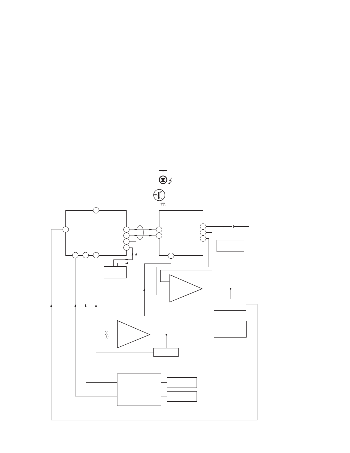
Self-diagnosis block diagram
D1201
TIMER/STANDBY
8
20 21 22
55
IC002
µProcessor
Audio
IC004
EEPROM
Audio AMP
5. AKB
6. H STOP
49
47
50
48
IC406
BUS
5. AKB
Q006
3
4
27
DC Detect
IC206
CXA2147
YCJ
IC1509
V Drive
43
35
34
6. HV STOP
IC502
HV Detector
Q1505
V Pulse Buffer
C Board
4. V.STOP (V Pulse)
3. OVP
2. OCP
IC651
OVP Buffer
OCP Buffer
OVP DETECT
OCP DETECT
– 6 –

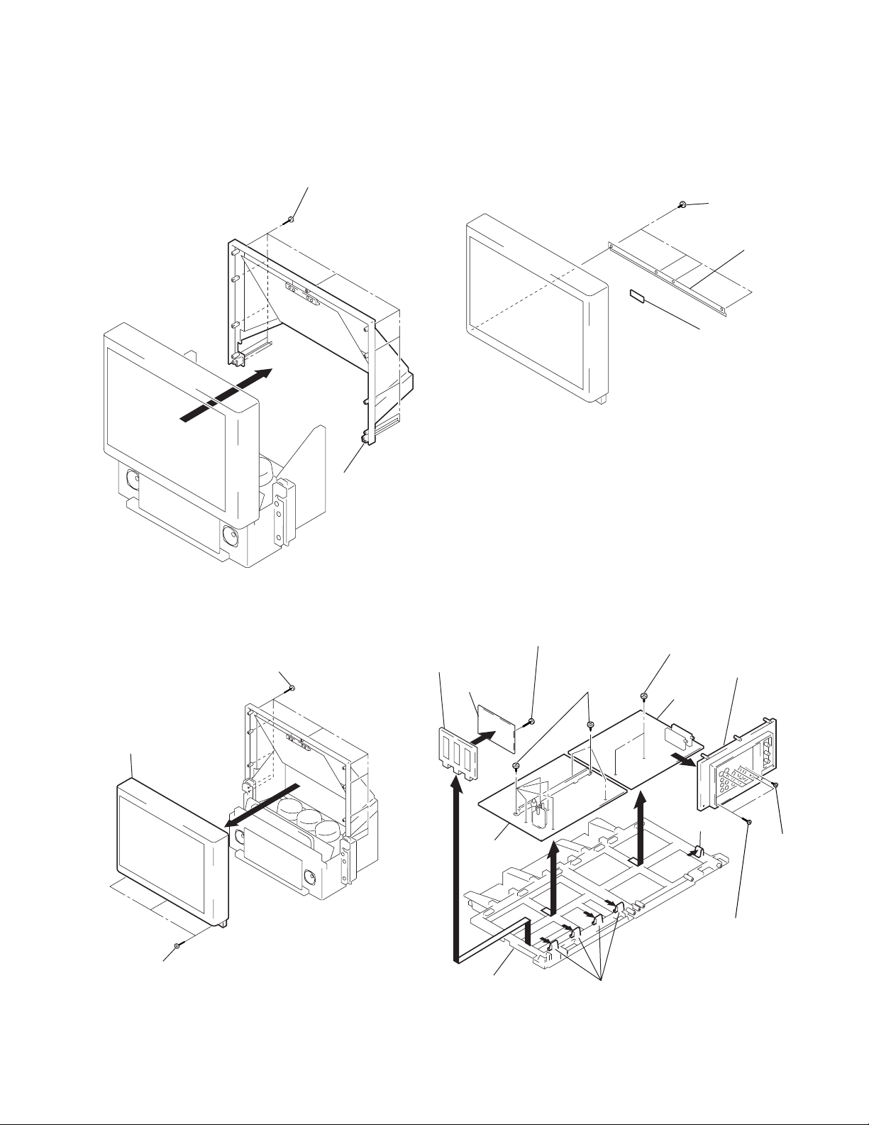
SECTION 2
DISASSEMBLY
2-1. REAR BOARD REMOVAL 2-3. SERVICE POSITION
1 Disconnect CN203
on A board.
From CG board CN1304.
(The extension cable is not
supplied because of the
countermeasure for radiation.)
2 Covers
Cut them off with a plier or the like
from chassis assembly in case of
checking printed circuit boards.
After checking, turn over the covers
and secure them with screws.
2 Rear board
A board
CN203
G board
KP-XR432K90/XR432N90
RM-Y906K RM-Y906
1 Nine screws
(Screw, tapping haxagon head)
2-2. CHASSIS ASSY REMOVAL
1 Three screws
(Screw, tapping haxagon head)
Chassis assembly
Screws
(+BVTP3x12)
2-4. HA AND HB BOARD REMOVAL
8 HB board
7 Three screws
(+BVTP 3x12)
4 HA bracket
Panel ASSY, Control
1 Four screws
(Screw, tapping haxagon head)
2
3 Four screws
(+BVTP 3x12)
6 HA board
2 Chassis assy
5 Three screws
(+BVTP 3x12)
– 7 –
KP-XR432K90/XR432N90
RM-Y906K RM-Y906
2-5. MIRROR COVER REMOVAL
1 Sixteen screws
(Screw, tapping haxagon head)
2-7. HC BOARD REMOVAL
1 T w o screws
(+BVTP 4x12)
2 L screen holder
3 HC board
2 Mirror cover
2-6. BEZNET ASSY REMOVAL
2 T w elve screws
(Screw, tapping haxagon head)
3 Beznet assy
1 Three screws
(Screw, tapping haxagon head)
2-8. A, G AND FA BOARDS REMOVAL
!¡ FA board bracket
!™ FA board
6 G board
Main bracket
0 Screw
(+BVTP 3x12)
4 Eight screws
(+BVTP 3x12)
5 Claws
7 T w o screws
(+BVTP 3x12)
3 T erminal board
9 A board
8 Claw
2 Seven screws
(+BVTP 3x12)
1 T w o screws
(Screw, tapping haxagon head)
– 8 –

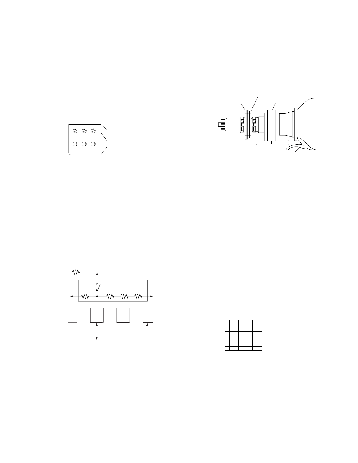
2-9. PICTURE TUBE REMOVAL
CAUTION: Removing the arrow-marked
screws is strictly prohibited.
If removed, it may cause liquid spill.
Lens
Picture tube
2 Four screws
(Screw, tapping
haxagon head)
KP-XR432K90/XR432N90
RM-Y906K RM-Y906
4 Four screws
(Screw, tapping haxagon head)
5 Lens
9 Four screws
(+BVTP 4x12)
0 Picture tube
8 Diflection yoke
7 Neck assy
6 CR board
3
2-10. HIGH-VOLTAGE CABLE INSTALLATION
AND REMOVAL
(1) Removal
1 Rubber cap
2 HV cable
turn 90°
(2) Installation
1 Four screws
(Screw, tapping haxagon head)
Gutter
1 HV cable
Hook
– 9 –
SECTION 3
SET-UP ADJUSTMENTS
KP-XR432K90/XR432N90
RM-Y906K RM-Y906
3-1. SCREEN VOL T AGE ADJUSTMENT
(COARSE ADJUSTMENT)
1. Receive the Monoscope signal.
2. Set 50% BRIGHTNESS and minimum PICTURE.
3. Turn the red VR on the FOCUS block all the way to the left
and then gradually turn it to the right until the point where you
can see the retrace line.
4. Next gradually turn it to the left to the position where the
retrace line disappears.
R G B
SCREEN
R G B
FOCUS
FOCUS block
Fig. 3-1
3-2. SCREEN (G2) ADJUSTMENT
(FINE ADJUSTMENT)
Fine Mode is recommended to set screen controls to their optimal
condition. It is necessary to build the simple jig, illustrated below,
using 3-watt resistors. Please note, that if the proper voltage is not
obtained with their listed values, resistors, then please increase or
decrease one of the values in the resistor network to obtain the
correct voltage.
1. Select VIDEO1 mode without signals.
2. Connect G2 JIG.
3. SW on JIG.
4. Connect an oscilloscope to the TP701(KR), TP732(KG) and
TP761(KB) of CR board, CG board and CB board.
5. Adjust R, G and B screen voltage to 168-172V with screen
VR on the Focus block.
K
G2 JIG
3.3k 5.6k 5.6k 5.6k
200V GND
SW
the mode Cover the both green and red picture lenses with the
lens caps is aligned the same as was done for green.
Note: Instead of items 3 and 6, you can cut off the unnecessary
color beams by controlling the service mode VPNT 28 RON,
29 GON, and 30 BON.
4-pole magnet
2-pole magnet
Fig. 3-3
Deflection yoke
Anode cap
3-4. FOCUS LENS ADJUSTMENT
In this adjustment, use the remote commander in the
service mode.
For details of the usage of the service mode and the remote
commander, please refer the item 3-9. ELECTRICAL
ADJUSTMENT BY REMOTE COMMANDER.
1. Loosen the lens screw.
2. Set to the service mode.
3. Receive the all-white signal.
4. Cover the both red and blue picture lenses with the lens caps
to show only the green color.
5. Set to PJE, and press 6 to display the test signal (crosshatch)“
on the screen.
6. Turn the green lens to adjust to the optimum focus point with
the test signal.
7. Tighten the lens screw.
8. Cover the both green and blue picture lenses with the lens caps
to show only the red color.
9. Set to PJE, and press 6 to display the test signal (crosshatch)“
on the screen.
10. Adjust red CRT lens just the same as green.
11. Cover the both green and red picture lenses with the lens caps
to show only the blue color.
175 ± 2V
GND
pedestal level
Fig. 3-2
3-3. DEFLECTION YOKE TIL T ADJUSTMENT
1. Receive the Monoscope signal.
2. Set in service mode.
3. Cover the both red and blue picture lenses with the lens caps
to show only the green color.
4. Loosen the deflection yoke set screw and align the tilt of the
Deflection Yoke so that the bars at the center of the
monoscope pattern are horizontal.
5. After aligning the deflection yoke, fasten it securely to the
funnel-shaped portion (neck) of the CRT.
6. The tilt of the deflection yoke for red is aligned in the mode
Cover the both green and blue picture lenses with the lens caps
and the tilt of the deflection yoke for blue is aligned with in
Test signal
Fig. 3-4
12. Set to PJE, and press 6 to display the test signal (crosshatch)“
on the screen.
13. Adjust blue CRT lens just the same as green.
14. After adjusting the items 3-5. Focus VR Adjustment, 3-6. 2Pole Magnet Adjustment and 3-7. 4-Pole Magnet Adjustment,
adjust again to the optimum focus point.
*:Every time you press 6, the test signal changes to
“crosshatch+video signal” - “dots+video signal” -
“crosshach(black)” - “dots(black)” - off.
Note: Instead of items 4, 8 and 11, you can cut off the unnecessary
color beams by controlling the service mode VPNT 28 RON,
29 GON, and 30 BON.
– 10 –

KP-XR432K90/XR432N90
/
x
y
x : y = 1:1.5 (BIue)
x : y = 1:1 (Green, Red)
Use the center dot
RM-Y906K RM-Y906
3-5. FOCUS VR ADJUSTMENT
1. Set to the service mode.
2. Receive the all-white signal.
3. Cover the both red and blue picture lenses with the lens caps
to show only the green color.
4. Set to PJE, and press 6 to display the test signal (crosshatch)
on the screen.
5. Turn the green focus VR on the focus block to adjust to the
optimum focus point with the test signal.
6. Cover the both green and blue picture lenses with the lens caps
to show only the red color.
7. Set to PJE, and press 6 to display the test signal (crosshatch)
on the screen.
8. Turn the red focus VR on the focus block to adjust to the
optimum focus point with the test signal.
9. Cover the both green and red picture lenses with the lens caps
to show only the blue color.
10. Set to PJE, and press 6 to display the test signal (crosshatch)
on the screen.
11. Turn the blue focus VR on the focus block to adjust to the
optimum focus point with the test signal.
12. After adjusting the items 3-4. Focus Lens Adjustment, 3-6. 2Pole Magnet Adjustment and 3-7. 4-Pole Magnet Adjustment,
adjust again to the optimum focus point.
Note: Instead of items 3, 6 and 9, you can cut off the unnecessary
color beams by controlling the service mode VPNT 28 RON,
29 GON, and 30 BON.
Use the center dot
Fig. 3-7
3-7. 4-POLE MAGNET ADJUSTMENT
1. Receive the Dot signal.
2. Set in service mode.
3. Cover the both red and blue picture lenses with the lens caps
to show only the green color.
4. Turn the green focus VR on the focus block to the left and set
to underfocus to enlarge the spot.
5. Now align the 4-Pole Magnet so that the enlarged spot
becomes a perfect circle for green and red.
6. Perform the same alignment for blue.
Scanning line visible.
A
Minimize both A and B.
Lens
Fig. 3-5
B
Center of crosshatch
Fig. 3-6
3-6. 2-POLE MAGNET ADJUSTMENT
(GREEN,RED)
1. Receive the Dot signal.
2. Set in service mode.
3. Cover the both red and blue picture lenses with the lens caps
to show only the green color.
4. Turn the green focus VR on the focus block to the right and
set to overfocus to enlarge the spot.
5. Now align the 2-Pole Magnet so that the enlarged spot is in
the center of the Just Focus spot.
6. Align the green focus VR and set for just (precise) focus.
7. Perform the same alignment for red.
Fig. 3-8
3-8. DEFOCUS ADJUSTMENT (BLUE)
Note: Please adjust the blue dot to be slightly larger than red and
green dots. This adjustment provides a more pleasing picture
to the customer.
1. Select the video menu and set the mode to “VIVID” mode.
2. Set to the service mode.
3. Change TV mode to the video input mode.
4. Set to PJE, and press 6 to display the test signal (dots) on the
screen.
5. Turn the blue focus VR on the focus block to adjust to the
diameter of the dots as shown in the figure below.
[Focus adjustment point]
Lmm Max
Inch
L
43"
6
Fig. 3-9
– 11 –
KP-XR432K90/XR432N90
2
5
8
0
1
4
7
3
6
9
ENTER
JUMP
GUIDE
INDEX
RESET
MENU
POWER
MUTING
FREEZE
AUDIO
ANT
TV/VIDEO
DISPLAYMTS/SAP
CC
PICTURE
MODE
POSITION ACTIVE
SWAP PIP
TV/VTR
SYSTEM
OFF
DVD/VTR SAT/CABLE
TV
DVD/
VTR
SAT/
CABLE
FUNCTION
SLEEP
m
N
M
xz
X
TV
RM-Y906K RM-Y906
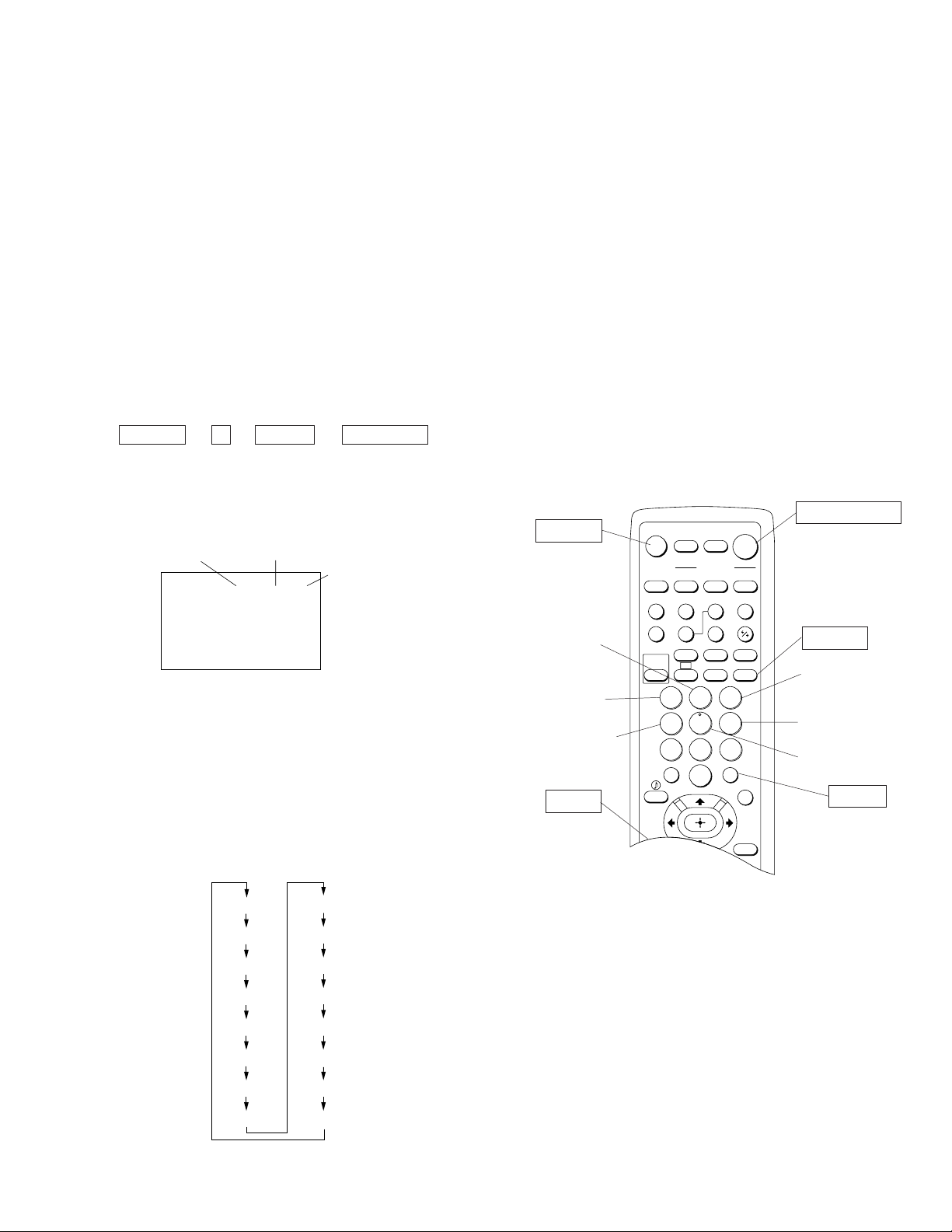
3-9. ELECTRICAL ADJUSTMENT BY REMOTE
COMMANDER
By using Remote Commander (RM-Y906/Y906K),all circuit
adjustments can be made.
NOTE : Test Equipment Required.
1. Pattern Generator (with component outputs)
2. Frequency counter
3. Digital multimeter
4. Audio oscillator
1. METHOD OF SETTING THE SER VICE ADJUSTMENT MODE
SERVICE MODE PROCEDURE
1. Standby mode. (Power off)
2. DISPLAY n 5 n VOL (+) n TV POWER
on the Remote Commander.
(Press each button within a second.)
SERVICE MODE ADJUSTMENT
Category Adjustment item
DATA
SERVICE VPNT VPOS 031
000000 00
7. If you want to recover the latest v alues press - then [ENTER] to
read the memory.
8. Press [MUTING] then [ENTER] to write into memory.
9. Turn power off.
Note: Press 8 then [ENTER] on the Remote Commander to initialize
or turn set off and on to exit.
2. MEMORY WRITE CONFIRMATION METHOD
1. After adjustment, remove the plug from AC outlet, and then
replace the plug in AC outlet again.
2. Turn the power switch ON and set to Service Mode.
3. Call the adjusted items again and confirm they were adjusted.
3. ADJUSTING BUTTONS AND INDICATOR
TV POWER ON
MUTING
(SCREEN DISPLAY)
3. The SCREEN displays the item being adjusted.
4. Press 1 or 4 on the Remote Commander to select the
adjustment item.
5. Press 3 or 6 on the Remote Commander to change the data.
6. Press 2 or 5 on the Remote Commander to select the
category.
Every time you press 2(Category up), Service mode changes
in the order as shown below.
VPNT
VPNV
VPNS
PJE
3DCM
TONE
DSP
MC
SC
IC
PP
DAC
PI
ID
CCD
OP
Category up
Adjustment item up
Adjustment item down
VOL (+)
RM-Y906/Y906K
Note : When the PJE mode is activated, which displays an
internally generated signal, several buttons on the remote
commander will have different functions than listed
above. Therefore, when in the PJE mode, refer to page 17
for button functions.
DISPLAY
Data up
Data down
Category down
ENTER
– 12 –
KP-XR432K90/XR432N90
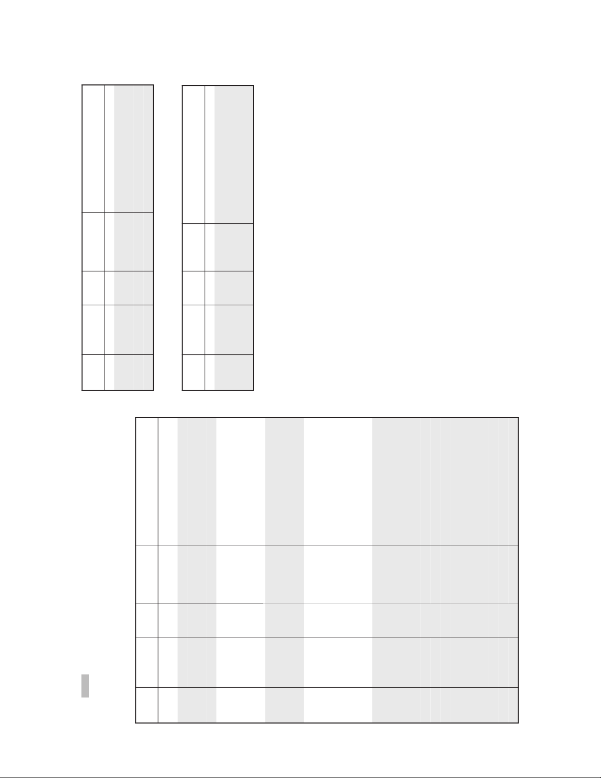
METI
REBMUN
TNEMTSUJDA
METI
ATAD
EGNAR
DRADNATS
ATAD
ETON
0SOPV36-013NOITISOPV
1ZISV36-013EZISV
2 MOCV
3-0
0
PMOCV
3
NILV
51-0
7
YTIRAENILV
4
OCSV
51-0
7
NOITCERROCEVRUCSV
5
SOPH
51-0
7
NOITISOPH
6ZISH36-013EZISH
7PMAP36-013PMANIP
8NIPU51-07 NOITROTSIDNIPRENROCREPPU
9NIPL51-07 NOITROTSIDNIPRENROCREWOL
01AHPP51-05 ESAHPNIP
11
CFA 3-0
2
NIAGPOOLCFA
21
WOBV
51-0
7 WOBV
31
GNAV
51-0
7
ELGNAV
41
FER
3-0
3
NOITISOPESLUPECNEREFER
51VRDR36-013NIAGEVIRDDER
61VRDB36-013NIAGEVIRDEULB
71TUCR51-07 FFOTUCDER
81TUCB51-07 FFOTUCEULB
91NOCS51-07 TSARTNOCBUS
02EUHS51-07 EUHBUS
12LOCS51-07 ROLOCBUS
22 2MDC
1,0
0
2EDOMNWODTNUOC
32
XIPD
1,0
1
ERUTCIPCIMANYD
42
CTON
1,0
0
PARTAMORHCY
52
MORC
51-0
7
0FPARTAMORHC
62
TOT
1,0
0
RETLIFTOTAMORHC
72
FPHS
3-0
3
0FSSENPRAHS
82
NOR
1,0
1
NODER
92
NOG
1,0
1
NONEERG
03
NOB
1,0
1
NOEULB
13
LOCD
1,0
1
ROLOCCIMANYD
23 DMDC
1,0
0
NWODTNUOCV
33
KLBL
51-0
31
HTDIWKNALBEDIS-TFEL
43
KLBR
51-0
31
HTDIWKNALBEDIS-THGIR
53
CERP
3-0
1
NIV.PMOCROFLEVELREVOERP
63
YERP
3-0
1
NIYROFLEVELREVOERP
METI
REBMUN
TNEMTSUJDA
METI
ATAD
EGNAR
DRADNATS
ATAD
ETON
0VRBS36-072DIVIVROFSSENTHGIRBBUS
1
VMMG
3-0
2
DIVIVROFLEVELAMMAG
2
VCDY
1,0
1
DIVIVROFOITARREFSNARTCD-Y
3 VLBA
1,0
1
DIVIVROFEDOMLBA
4 VIXA
1,0
0
DIVIVROFY-G,Y-RSIXA
METI
REBMUN
TNEMTSUJDA
METI
ATAD
EGNAR
DRADNATS
ATAD
ETON
0SRBS36-072DRADNATSROFSSENTHGIRBBUS
1
SMMG
3-0
2
DRADNATSROFLEVELAMMAG
2
SCDY
1,0
0
DRADNATSROFOITARREFSNARTCD-Y
3
SLBA
1,0
1
DRADNATSROFEDOMLBA
4 SIXA
1,0
0
DRADNATSROFY-G,Y-RSIXA
RM-Y906K RM-Y906
VPNV (Video Processor NTSC Vivid)
VPNS (Video Processor NTSC Standard)
in the sets individually. Basically, there is no need to change data, too.
of replacing printed circuit boards or devices.
• Usually, there is no need to adjust except for VPNT and PJE. Use data as a reference in case
4. SERVICE MODE LIST
Note: • shaded items are fixed. There is no need to change data. Others are different a little
VPNT (Video Processor NTSC)
– 13 –
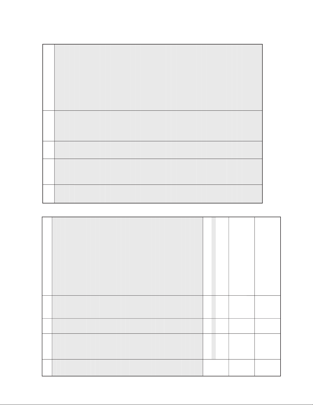
KP-XR432K90/XR432N90
METI
REBMUN
TNEMTSUJDA
METI
ATAD
EGNAR
DRADNATS
ATAD
ETON
0
SIDF
1,0
0
JDAENIFFOYALPSIDATADIGERTCELES
1
HDSO
552-1
13
NOITISOPHUNEMECIVRESDEJP
2
VDSO
552-1
52
NOITISOPVUNEMECIVRESDEJP
3
TSVF
552-0
52
TRATSTSUJDAENIFFOREBMUNENIL
4
TS1V
552-0
0
ATADTRATS1V
5
UC1V
552-0
26
ATADPUTNUOC1V
6 PHOC
552-0
0 JDAHGUORFOESAHP-H
7
PHIF
552-0
491
JDAENIFFOESAHP-H
8
PHPT
552-0
26
NRETTAPTSETFOESAHP-H
9
PHFD
552-0
522
SUCOFCIMANYDFOESAHP-H
01
GHFD
721-821-
08-
SUCOFCIMANYDFONIAG2-H
11
GVFD
721-821-
51-
SUCOFCIMANYDFONIAG2-V
21
lMWP
552-0
0
lMWP
31
2MWP
552-0
23
NRETTAPTSET.IGEROTUAFOESAHP-H
41
DLBH
552-0
442
ENILVEULBDENRUTERFOESAHP-H
51
WLBH
36-0
32
ENILVEULBDENRUTERFOHTDIWESLUP
61
PKLB
552-0
72
ESLUPKNALBTRATS
71
VGOC
721-821-
)1*(X
IGEROTUAFOATADTESFFOTNECVNEERG
81
VROC
721-821-
)1*(X
IGEROTUAFOATADTESFFOTNECVDER
91
VBOC
721-821-
)1*(X
IGEROTUAFOATADTESFFOTNECVEULB
02
HGOC
721-821-
)1*(X
IGEROTUAFOATADTESFFOTNECHNEERG
12
HROC
721-821-
)1*(X
IGEROTUAFOATADTESFFOTNECHDER
22
HBOC
721-821-
)1*(X
IGEROTUAFOATADTESFFOTNECHEULB
32
VGOS
721-821-
)1*(X
IGEROTUAFOATADTESFFOWEKSVNEERG
42
VROS
721-821-
)1*(X
IGEROTUAFOATADTESFFOWEKSVDER
52
VBOS
721-821-
)1*(X
IGEROTUAFOATADTESFFOWEKSVEULB
62
HGOS
721-821-
)1*(X
IGEROTUAFOATADTESFFOWEKSHNEERG
72
HROS
721-821-
)1*(X
IGEROTUAFOATADTESFFOWEKSHDER
82
HBOS
721-821-
)1*(X
IGEROTUAFOATADTESFFOWEKSHEULB
92
RRE
DEXIF
0 EDOCRORREIGEROTUA
03
MTDA
552-0
441
IGEROTUAFOATADD/ATEGOTGNIMIT
13
PUV
552-1
1
NOITISOPVREPPUNRETTAPIGEROTUA
23
DIMV
552-1
201
NOITISOPVELDDIMNRETTAPIGEROTUA
33
WOLV
552-1
212
NOITISOPVREWOLNRETTAPIGEROTUA
43
RPH
015-1
1
NOITISOPHNRETTAPIGEROTUA
NRG
TNEC115-215-000/000TNECV/HNEERG
WEKS115-215-000/000WEKSV/HNEERG
EZIS
115-215-
091-/07-
EZISV/HNEERG
NIL115-215-xxxx/xxxxNILV/HNEERG
YEK115-215-xxxx/xxxxYEKV/HNEERG
NIP115-215-172/xxxxNIPV/HNEERG
ULB
TNEC115-215-000/000TNECV/HEULB
WEKS115-215-031-/080WEKSV/HEULB
EZIS115-215-622-/02-EZISV/HEULB
NIL115-215-xxxx/781NILV/HEULB
YEK115-215-511-/xxxxYEKV/HEULB
NIP115-215-891/xxxxNIPV/HEULB
DER
TNEC115-215-000/000TNECV/HDER
WEKS115-215-031-/080WEKSV/HDER
EZIS115-215-602-/16-EZISV/HDER
NIL115-215-xxxx/591NILV/HDER
YEK115-215-421/xxxxYEKV/HDER
NIP115-215-052/xxxxNIPV/HDER
METI
REBMUN
TNEMTSUJDA
METI
ATAD
EGNAR
DRADNATS
ATAD
ETON
0
DMRN
3-0
0
EDOMRECUDERESION
1
OCYD
51-0
2
∆ GNITTESLEVELGNIROCY
2
AGYD
51-0
01
∆ GNITTESNIAGY
3
OCCD
51-0
5
∆ GNITTESLEVELGNIROCC
4
AGCD
51-0
5
∆ GNITTESNIAGC
5 DLES
1,0
1
TCELES ∆ RETLIFLANGISY
6 AG2D
7-0
4
∆ GNITTESNIAGdn2C/Y
7 HRTV
3-0
1
GNITTESSISERETSYHCNYSHRTV
8
RRTV
3-0
1
GNITTESECNEREFERCNYSHRTV
9
RSDL
3-0
2
ECNEREFERLANGISDL
01
GPAV
7-0
5
NIAGERUTREPAV
11 IPAV
13-0
11
TNIOPTREVNIERUTREPAV
21
TFPY
3-0
0
PATRETLIFGNIKAEPY
31
GFPY
51-0
9
NIAGRETLIFGNIKAEPY
41
SP1V
3-0
2
ROTCELESENIL-1LACITREV
51 SGEV
3-0
1
ROTCELESEGDELACITREV
61
N3CC
1,0
0
RETLIFMOCENIL-3LANGISC
71
PDH
7-0
4
ESAHPLATNOZIROHDH
81
LDC
7-0
4
YALEDC
91
LSSH
51-0
21
LEVELECILSCNYSH
02
LSSV
51-0
8
LEVELECILSCNYSV
12
FLPH
1,0
1
RETLIFLLPH
22
FLPB
1,0
0
RETLIFLLPTSRUB
32
FCSF
1,0
1
NIAGRETLIFCSF
42
GFLP
1,0
1
NIAGRETLIFLLP
52
DAXE
1,0
1
NIDALANRETXE
62
SSM
1,0
0
LANGISNOITOMDECROF
72 TUOC
3-0
2
TUPTUOLANGISC
82
SPAY
3-0
1
ERUTREPAY
92
SDSN
3-0
0
.TCETEDLANGISDTSNON
03
PPC
3-0
0
EGNARDA&ESLUPPMALC
13
OCHY
3-0
1
GNIROCLANGIS.QERFHGIHY
23
OCPY
1,0
0
FFOGNIROCRETLIFKAEPY
33
RLIK
51-0
3
ECNEREFERRELLIK
43
SPGB
51-0
4
NOITISOPTRATSPGB
53
WPGB 51-0
01
HTDIWPGB
63
LCDA
3-0
2
YALEDKCOLCDA
73 FRWP
1,0
0
ECNEREFERHTDIWESLUP
83
GCHY
1,0
0
NIAG2/1GNIROCLANGIS.QERFHGIHY
93 2GKC
1,0
1
TIBTSETROTARENEGKCOLC
04 EGKC
1,0
0
TIBTSETROTARENEGKCOLC
RM-Y906K RM-Y906
3DCM (3D Comb Filter)
PJE (Projection TV Engine)
– 14 –
∗ 1 : Set correctly by the automatic resistration adjustment.
xxxx : Cannot change.

KP-XR432K90/XR432N90
METI
REBMUN
TNEMTSUJDA
METI
ATAD
EGNAR
DRADNATS
ATAD
ETON
0
SABR
36-0
93
ATADSSABRESUFOEULAVTESER
1
ERTR
36-0
53
ATADELBERTRESUFOEULAVTESER
2 HEBB
51-0
-
YCNEUQERFHGIHEBB
3
LEBB
11-0
-
YCNEUQERFWOLEBB
4 EFUS
7 -
TCEFFEDNUORRUS
METI
REBMUN
TNEMTSUJDA
METI
ATAD
EGNAR
DRADNATS
ATAD
ETON
0
H0BT
552-0
84
ESRAOC)R+L(TCEFFEDNUORRUSURT
1 L0BT
552-0
0
ENIF)R+L(TCEFFEDNUORRUSURT
2 H1BT
552-0
46
ESRAOC)R-L(TCEFFEDNUORRUSURT
3 L1BT
552-0
0
ENIF)R-L(TCEFFEDNUORRUSURT
4 H2BT
552-0
46
ESRAOC)C(TCEFFEDNUORRUSURT
5 L2BT
552-0
0
ENIF)C(TCEFFEDNUORRUSURT
6 HFBT
552-0
561
ESRAOC)S(TCEFFEDNUORRUSURT
7
LFBT
552-0
621
ENIF)S(TCEFFEDNUORRUSURT
8 H0CT
552-0
09
ESRAOC)S(TCEFFEDNUORRUSURT
9
L0CT
552-0
031
ENIF)S(TCEFFEDNUORRUSURT
01
H1CT
552-0
11
ESRAOC)R,L(TCEFFEDNUORRUSURT
11
L1CT
552-0
001
ENIF)R,L(TCEFFEDNUORRUSURT
21
HDAS
552-0
46
ESRAOCLEVELECAPSSRS
31
LDAS 552-0
0
ENIFLEVELECAPSSRS
41
H0BS
552-0
29
ESRAOCLEVELRETNECSRS
51
L0BS
552-0
0
ENIFLEVELRETNECSRS
METI
REBMUN
TNEMTSUJDA
METI
ATAD
EGNAR
DRADNATS
ATAD
ETON
0RDYM13-022EVIRDYNIAM
1UHSM36-013EUHBUSNIAM
2LCSM36-013ROLOCBUSNIAM
3
DPUM
51-0
7
TESFFOLATSEDEPUNIAM
4
DPVM
51-0
7
TESFFOLATSEDEPVNIAM
5YLDM3-00 YALEDYNIAM
6P2UM51-07 TESFFOLATSEDEP2UNIAM
7P2VM51-07 TESFFOLATSEDEP2VNIAM
8
D2YM
13-0
91
EVIRD2YNIAM
9
D2UM
13-0
11
EVIRD2UNIAM
01
D2VM
13-0
11
EVIRD2VNIAM
11
ERPM
3-0
3
REVO-ERPNIAM
METI
REBMUN
TNEMTSUJDA
METI
ATAD
EGNAR
DRADNATS
ATAD
ETON
0RDYS13-082EVIRDYBUS
1UHSS36-013EUHBUSBUS
2LCSS36-013ROLOCBUSBUS
3DPUS51-07 TESFFOLATSEDEPUBUS
4DPVS51-07 TESFFOLATSEDEPVBUS
5 YLDS
3-0
0
YALEDYBUS
6 P2US
51-0
7
TESFFOLATSEDEP2UBUS
7
P2VS
51-0
7
TESFFOLATSEDEP2VBUS
8 D2YS
3-0
02
EVIRD2YBUS
9 D2US
51-0
11
EVIRD2UBUS
01
D2VS 51-0
11
EVIRD2VBUS
11
ERPS
3-0
3
REVO-ERPBUS
METI
REBMUN
TNEMTSUJDA
METI
ATAD
EGNAR
DRADNATS
ATAD
ETON
0 RDCP
51-0
7
ROLOCPIP
1
RDHP
51-0
7
EUHPIP
2 CFAP
3-0
2
NIAGPOOLCFAPIP
3
DATP
51-0
7
TNEMTSUJDA0FPARTPIP
4 TOTP
1,0
0
RETLIFTOTAMORHCPIP
5
NCSP 51-0
7
TSARTNOCBUSPIP
6
CDYP
7-0
0
NARTCDYPIP
7
PHSP
1,0
1
0FSSENPRAHSPIP
8
KSMP
1,0
0
KSAMNOISIVORCAMPIP
METI
REBMUN
TNEMTSUJDA
METI
ATAD
EGNAR
DRADNATS
ATAD
ETON
0PHGB51-001NOITISOPHPIP
1NHGB51-07 LANGISONROFNOITISOPHPIP
2PVGB51-07 NOITISOPVPIP
3
TIB6
1,0
1
XIRTAM)6PIKS/6TRAMS(TIB6
4PHAM51-07 NOITISIUQCAHNIAM
5
PVAM
552-0
32
NOITISIUQCAVNIAM
6PHAS51-07 NOITISIUOCAHBUS
7
PVAS 552-0
32
NOITISIUQCAVBUS
8
SCED
13-0
81
SRETSIGERREDOCEDBUS
9 MCED 13-0
81
SRETSIGERREDOCEDNIAM
01
SID
721-0
66
GNITTESYALPSID
11
ZISB
51-0
2
EZISREDROB
21
DEPV
51-0
31
TESFFOLATSEDEPV
31
DEPU
51-0
31
TESFFOLATSEDEPU
RM-Y906K RM-Y906
SC (Sub Chroma Decoder)
IC (Inset Chroma Decoder)
PP (Picture In Picture Vseries Only)
TONE (Tone Control)
DSP (Digital Signal Processor)
– 15 –
MC (Main Chroma Decoder)

KP-XR432K90/XR432N90
METI
REBMUN
TNEMTSUJDA
METI
ATAD
EGNAR
DRADNATS
ATAD
ETON
0HSVU36-013EUHBUSVUY
1CSVU36-013ROLOCBUSVUY
METI
REBMUN
TNEMTSUJDA
METI
ATAD
EGNAR
DRADNATS
ATAD
ETON
0 AERA
3-0
0 DIAERA
1
SRES
3-0
0
DISEIRES
2
PHCV
3-0
0
DIPIHCV
METI
REBMUN
TNEMTSUJDA
METI
ATAD
EGNAR
DRADNATS
ATAD
ETON
0
PHCC
36-0
93
SDX/CC&XEDNIROFISOPHDSO
1
NHCC
36-0
92
NOITCNUFON
METI
REBMUN
TNEMTSUJDA
METI
ATAD
EGNAR
DRADNATS
ATAD
ETON
0 PSID 36-0
9
NOITISOPHDSO
1 lWF
7-0
2
WODNIW1DLEIF
2 2WF
7-0
3
WODNIW2DLEIF
METI
REBMUN
TNEMTSUJDA
METI
ATAD
EGNAR
DRADNATS
ATAD
ETON
0HPIP-NOITISOPHPIP
1VPIP-NOITISOPVPIP
2DSYP-YALEDTCELESPIP
3LDYP-YALEDYPIP
4LDHP-YALEDESLUP-H
5DVMP- YALEDESLUP-VNIAM
6DVIP- YALEDESLUP-VTESNI
7NOCP-TSARTNOCTESNI
8YMRF-YEMARF
9REPI-Y-RJIATSEDEPPIP
01BEPI-Y-BLATSEDEPPIP
11SPCP-PLCPIP
21FPCP-SELCYCPLCPIP
31LLPP- TNATSNOCEMITLLPPIP
41RNVP- NOITCUDERESIONESLUPPSVPIP
RM-Y906K RM-Y906
DAC (D/A Converter)
PI (Picture In Picture S Series only)
ID (Identification)
– 16 –
CCD (Closed Caption Decoder)
OP (Option)
KP-XR432K90/XR432N90
RM-Y906K RM-Y906
3-10. REGISTRATION ADJUSTMENT (PJE)
• FUNCTION OF BUTTONS OF REMOTE
COMMANDER FOR PJE MODE.
DVD/
SAT/
VTR
CABLE
FUNCTION
DVD/VTR SAT/CABLE
FREEZE
SWAP PIP
m
N
AUDIO
POSITION ACTIVE
xz
ANT
SLEEP
CC
2
1
5
4
8
7
JUMP
0
VOL CH
TV
ENTER
3
6
9
POWER
TV
TV
M
TV/VIDEO
DISPLAYMTS/SAP
GUIDE
MENU
Color select
n
BLUnRED
GRN
Test signal select
crosshach+video signal
dots+video signal
crosshach+black
dots+black
off
Mode select
Coarse adjustment
(
Fine adjustment
ENTER
Adjustment item
up
Adjustment item
down
INIT*
READ*
MUTING
SYSTEM
OFF
TV/VTR
X
PICTURE
MODE
INDEX
RESET
CODE SET
data up/down
INIT*: Press 7, "INIT" green letters appear on the screen.
Then press ENTER, all the PJE data are reset.
READ*: Press 8, "READ" green letters appear on the screen.
Then press ENTER, all the PJE default data are
restored.
Note: Internal patterns are used for geometry and convergence
adjustments. However, sizing and centering must be done with
the use of an external generator. The recommended pattern
would be a monoscope, or equivalent pattern, which would
provide the means to adjust both the linearity and sizing of the
picture.
[SETUP FOR ADJUSTMENT]
• Current flow in circuit should be stable before attempting
adjustment. So wait 5 minutes after turning on the TV power.
• At the 4 insides of the screen, locate the middle. Use a tape
measure to identify the middle.
: middle
1. Set to the service mode by pressing quickly keys on the remote
commander in the standby mode in the following order:
[DISPLAY] n 5 n [VOL+] n [TVPOWER]
2. Change TV mode to the video input mode.
3. Change the VPNT mode to the PJE 00 FDIS.
PJE 00 00
FDIS
4. Set FDIS data to “01” to display the registration data of each
spot in the fine adjustment.
)
PJE 00 01
FDIS
5. Press 6 to display the test signal (crosshatch) on the screen.
6. Select GRN CENT(*) with the 1 and 4 keys on the remote
commander and check that the adjustment data is now “000”
both vertically and horizontally.
(H) (V)
GRN 000 000
CENT
*: In the factory preset, “GRN CENT” appears on the screen first.
In case of other colors “RED” or “BLU”, change color by
every pressing 3 key.
7. Cover the both red and blue picture lenses with the lens caps to
show only the green color.
SUB DEFLECTION ADJUSTMENT ITEM
Adjustment O : Yes – : No
Adjustment type
Display Adjustment item G R B
H/V H/V H/V
CENT CENT O/O O/O O/O
SKEW SKEW O/O O/O O/O
SIZE SIZE –/– O/O O/O
LIN LIN –/– O/– O/–
KEY KEY –/––/O –/O
PIN PIN –/O –/O –/O
– 17 –
KP-XR432K90/XR432N90
RM-Y906K RM-Y906
[GREEN REGISTRATION ADJUSTMENT]
<GREEN CENTER>
1. Select GRN CENT 1and 4 keys on the remote commander.
2. Adjust the center of crosshatch line goes the middle vertically
and horizontally (GRN CENT) with the joystick on the remote
commander.
GRN
CENT
<GREEN SKEW>
1. Select GRN SKEW with the 1and 4 keys on the remote
commander.
2. Adjust the crosshatch line goes straight vertically and horizontally with the joystick on the remote commander.
000
000
: Middle
<FINE ADJUSTMENT>
1. Press 9 key on the remote commander to shift to the fine
adjustment mode.
The green cursor (in the GRN mode) appears on the center of
the screen.
2. Use the 1and 4 keys or the joystick on the remote commander, move the cursor (see below) everywhere you want to
adjust and adjust with the joystic keys on the remote commander.
Marker movement by the 1 and 4 keys:
Press once the joystick the cursor turns green to white.
Then you can move the cursor up and down left and right every
where you want.
GRN
SKEW
000 000
<GREEN PINCUSHION>
1. Select GRN PIN with the 1and 4 keys on the remote
commander.
2. Adjust the crosshatch line goes straight horizontally with the
joystick on the remote commander.
GRN
XXXX 000
PIN
Note : These are required when either severe miss-adjustment or
data loss occurred.
Press once the joystick the cursor stops and returns green, you
can adjust around the cursor.
3. Press 9 key on the remote commander to shift to the coarse
adjustment mode.
– 18 –

KP-XR432K90/XR432N90
RM-Y906K RM-Y906
[RED REGISTRATION ADJUSTMENT]
<RED CENTER, SKEW>
1. Cover the blue picture lens with the lens cap to show the green
and red colors.
2. Press 3 key on the remote commander to shift the GRN mode
to the RED mode.
3. Select RED CENT or RED SKEW with the 1 and 4 keys
on the remote commander and adjust while tracking each other
alternately.
4. Adjust the red crosshatch lines go straight vertically and
horizontally and overlaps the green lines with the joystick on
the remote commander.
<RED SIZE, LINEARITY>
1. Select RED SIZE (vertically and horizontally) or RED LIN
(vertically) with the 1 and 4 keys on the remote commander and adjust while tracking each other alternately.
2. Adjust the red crosshatch lines go straight vertically and
horizontally and overlaps the green lines with the joystick on
the remote commander.
<RED KEY, PINCUSHION>
1. Select RED KEY or PINCUSHION with the 1 and 4 keys
on the remote commander and adjust while tracking each other
alternately.
2. Adjust the red crosshatch lines go straight horizontally and
overlaps the green lines
with the joystick on the remote commander.
Note : These are required when either severe miss-adjustment or
data loss occurred.
[BLUE REGISTRATION ADJUSTMENT]
1. Remove the lens cap from the blue picture lens to show full
color.
2. Press 3 key on the remote commander to shift the RED mode
to the BLU mode.
3. Adjust BLU CENT, BLU SKEW, BLU SIZE, BLU LIN, BLU
KEY and BLU PIN in the same procedure of the red registration adjustment.
[FINAL CHECK]
1. Store the new adjustment (offset) value on the remote control
by pressing [MUTING] and [ENTER].
2. Press the FLASH FOCUS button on the front panel.
(The Offset value is now automatically stored.)
3. Check that no error message appears.
If an error message appears, recheck.
Note: In case of replacing CRTs, adjust the set-up adjustments
(items 3-1 to 3-8) and the registration adjustment (item 3-10).
In case of replacing two or three CRTs at the same time,
replace and adjust one by one.
<FINE ADJUSTMENT>
1. Press 9 key on the remote commander to shift to the fine
adjustment mode.
The red cursor (in the RED mode) appears on the center of the
screen.
2. Use the 1 and 4 keys or the joystick on the remote commander, move the cursor everywhere you want to adjust and
adjust with the joystick on the remote commander.
– 19 –
KP-XR432K90/XR432N90
RM-Y906K RM-Y906
3-11. AUTO REGISTRATION ERROR CODE LIST
If an error code is displayed after the set has been fully adjusted, correctly, please check the following items: position, tilt and sizing. If
either of these adjustments are off, even slightly, the auto-registration pattern will not hit the four sensors properly. This occurs when the
internal generator patterns is being flashed on the screen for the sensors to read. Therefore, auto registration (called auto-focus) cannot
operate properly causing an error code to be displayed. In order for this function to operate properly, correct position, tilt and size must be
adjusted properly.
[ERROR CODE LIST]
ERROR
CODE
00 No Error
10 Sensor Output Level Low * Check wiring, beam position, sensor. 0 : Upper Center
20 Sensor Output Level High * Check OP-amp circuit. 0 : Upper Center
30 Adjustment Loop Counter Overflow * Check the registring information on the convergence board.
40 Regi Data Overflow
50 Regi Data Overflow
60 Offset Overflow
70 Offset Overflow
DISCRIPTION NOTE
1 : Middle Left
2 : Middle Right
3 : Lower Center
1 : Middle Left
2 : Middle Right
3 : Lower Center
* Check the convergence yoke driver ICs.
* Convergence patterns displayed are out of normal range.
* In case of multiple error, last error is displayed.
• ERROR CODE SCREEN DISPLAY
E 11 B
E 11 B
* Error code will be displayed on center of screen for 3 seconds.
• ERROR CODE DISPLAY IN REGI SERVICE MODE
PJE 2 9 1 4 0
ERR
ITEM NUMBER-29
SENSOR NUMBER
(ONLY "10"or "20")
ERROR CODE 40
G-0 (Blank)
R.G.B
R-1
B-2
R. G. B
SENSOR NUMBER
ERROR CODE 10
ERROR
[SENSOR POSITION]
0
12
SCREEN
3
0 : UPPER SENSOR
1 : LEFT SENSOR
2 : RIGHT SENSOR
3 : LOWER SENSOR
– 20 –

SECTION 4
CIRCUIT ADJUSTMENTS
4-1. TV INPUT SUB CONTRAST ADJUSTMENT
(VPNT-SCON)
1. Receive the color-bar signal.
2. Mode : Personal 1 or 2.
PICTURE : maximum
COLOR : maximum
BRIGHTNESS : center
TRINITONE : medium
SERVICE DATA VPNT SCON : 7
3. Set to service mode.
4. Connect an oscilloscope between pin 7 of CN204 (A board)
and ground.
5. Select “ VPNT-SCON ”, and adjust so that the wave from
level is 1.80 ± 0.05Vp-p.
6. Write the data into memory .
MUTING n ENTER
White
±
0.05Vp-p
1.80
KP-XR432K90/XR432N90
RM-Y906K RM-Y906
4-3.
COMPONENT INPUT SUB-HUE AND SUB-COLOR
ADJUSTMENT
1. Select VIDEO 4 and supply the color-bar signal.
VIDEO input
2. Mode : Personal 1 or 2.
PICTURE : maximum
COLOR : center
BRIGHTNESS : center
TRINITONE : medium
SERVICE DATA DAC UVSH : 31
SERVICE DATA DAC UVSC : 31
3. Set to service mode.
4. Connect an oscilloscope between pin 5 of CN204 (A board)
connecter and ground.
5. Select “ DA C-UVSH, UVSC ”, and adjust them to have VB1
= VB4 and VB2 = VB3 in the waveform levels.
6. Write the data into memory .
MUTING n ENTER
(DAC-UVSH, UVSC)
Black
Fig. 4-1
4-2. VIDEO INPUT SUB-HUE AND SUB-COLOR
ADJUSTMENT (VPNT-SHUE, SCOL)
1. Select VIDEO1 input and supply the color-bar signal.
2. Mode : Personal 1 or 2.
PICTURE : maximum
COLOR : center
BRIGHTNESS : center
TRINITONE : medium
SERVICE DATA VPNT-SHUE : 7
SERVICE DATA VPNT-SCOL : 7
3. Set to service mode.
4. Connect an oscilloscope between pin 5 of CN204 (A board)
connecter and ground.
5. Select “ VPNT-SHUE, SCOL ”, and adjust them to have VB1
= VB4 and VB2 = VB3 in the waveform levels.
6. Increase SCOL by 2 steps.
7. Write the data into memory .
MUTING n ENTER
VB1 VB2 VB3 VB4
Fig. 4-3
4-4. P & P SUB CONTRAST ADJUSTMENT
(SC-SYDR)
1. Receive the signal.
TV terminal (sub) : color-bar signal
VIDEO terminal (main) : no signal
2. Set to service mode and set to P & P mode.
3. Connect an oscilloscope between pin 7 of CN204 (A board)
and ground.
4. Select “ SC-SYDR ”, and adjust so that the wave from level
is 1.65 ± 0.05Vp-p.
5. Write the data into memory .
MUTING n ENTER
White
±
0.05Vp-p
1.65
Black
VB1 VB2 VB3 VB4
Fig. 4-2
Fig. 4-4
– 21 –
KP-XR432K90/XR432N90
RM-Y906K RM-Y906
4-5. SUB-HUE , SUB-COLOR AND MAIN
CONTRAST ADJUSTMENT (MC-MYDR,
MSHU, MSCL, SC-SSHU, SSCL)
1. Receive the color-bar signal.
2. Mode : Personal 1 or 2.
PICTURE : maximum
COLOR : center
BRIGHTNESS : center
TRINITONE : medium
SERVICE DATA MC-MYDR : 22
SERVICE DATA MC-MSHU : 31
SERVICE DATA MC-MSCL : 31
SERVICE DATA SC-SSHU : 31
SERVICE DATA SC-SSCL : 31
3. Set to service mode and set to P & P model .
4. Connect an oscilloscope between pin 5 of CN204 (A board)
connecter and ground.
5. Select “ MC-MYDR”, and adjust them to have VB1 = VB5
in the waveform levels.
6. Select “ MC-MSCL, SC-SSCL” and adjust so that the wave
form shows VB1=VB4 and VB5=VB8.
7. Select “ MC-MSHU, SC-SSHU” and adjust so that the wave
form shows VB2=VB3 and VB6=VB7.
8. Write the data into memory .
MUTING n ENTER
4-7. PIP POSITION ADJUSTMENT
(PI-PIPH, PIPV)
1. Set the PIP mode.
2. Receive the monoscope signal on the main/sub picture.
3. Check the sub picture position.
X1-X2
X1-X2
0.25sq
0.25sq
4. If necessary set to service mode and adjust "PIPH", "PIPV".
5. Write the data into memory .
MUTING n ENTER
Y1
Y2
X2X1
Fig. 4-7
VB1 VB2 VB3 VB4 VB5 VB6 VB7 VB8
Fig. 4-5
4-6. BAR DISPLAY POSITION ADJUSTMENT
(OP-DISP)
1. Receive the monoscope signal.
2. Set to service mode.
3. Push “ PICTURE +” . (Bar is displayed)
4. Select “ OP-DISP ” , and adjust so that the bar is as shown in
the figure.
5. Write the data into memory .
MUTING n ENTER
X1
Fig. 4-6
X2
X1 = X2
– 22 –
[ G BOARD]
KP-XR432K90/XR432N90
RM-Y906K RM-Y906
SECTION 5
SAFETY RELATED ADJUSTMENTS
5-1. HV REGULATION CIRCUIT CHECK AND
ADJUSTMENT
When replacing the following components marked with
on the schematic diagram always check HV regulation, and
if necessary re-adjust.
: C517
: C517, C521, C522
IC654, L504
T502, T504 (FBT)
D.Y, A board, G board
OPERATION CHECK
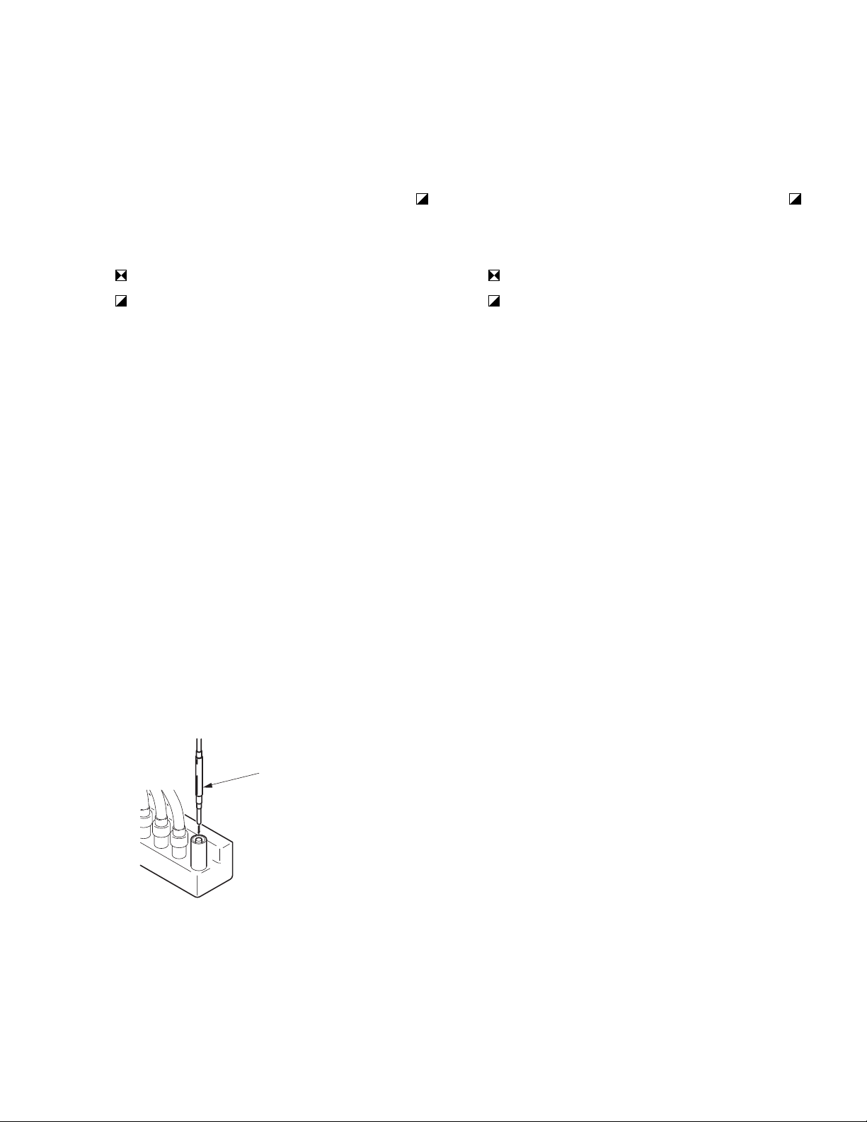
1. Connect a HV static voltmeter to the unconnected plug of
the high-voltage block. (Fig.5-1)
2. Power on the set.
3. Receive the dot signal. (PICTURE and BRIGHTNESS to
minimum)
4. Check that the HV static voltmeter is
reading 31.00
+0.95
-1.45
kVdc.
HV Regulation adjustment
1. Connect a HV static voltmeter to the unconnected plug of
the hight-voltage block.
2. Power on the set.
3. Receive the dot signal. (PICTURE and BRIGHTNESS to
minimum)
4. If anode voltage is 31.95kV or higher, replace C517 of 470PF/
2kV with that of 680PF/2kV , and check if the v oltage is within
the standard range.
5. If anode voltage is 29.66kV or lower , replace C517 of 470PF/
2kV with that of 100PF/2kV , and check if the v oltage is within
the standard range.
Remove the cap off from
the unused terminal and
cpmmect a static voltmeter
there.
5-2. HV HOLD DOWN CIRCUIT OPERATION
CHECK AND ADJUSTMENT
When replacing the following components marked with
on the schematic diagram always check hold-down voltage
and if necessary re-adjust.
: R536, R545
: C516, C536
D506, D507, D522
IC206, IC502, IC654
L504, R511, R522, R536, R538, R545,
R548, R584
T502, T504 (FBT)
D.Y, A board, G board
OPERATION CHECK
1. Remove CN652 connecter.
2. Short-circuit across TP-PROT and ground.
3. Connect a HV static voltmeter to the unconnected plug of
the high-voltage block.
4. Connect a 220 Ω/200W variable resistor, across pin 2 and
pin 1 of CN652 and connect an external dc power supply
unit (200V, class 2A) to pin 3 of CN652.
5. First turn on the external power supply (+B=135V), then turn
on the power of the set.
6. Receive the dot signal. (PICTURE and BRIGHTNESS to
minimum)
7. Gradually increase the value of the external dc po wer supply
and check that the hold-down circuit operates at a static voltmeter reading of 33.5±0.95kVdc when the raster disappears.
HV HOLD-DOWN ADJUSTMENT
1. Repeat steps 1 ~ 7 as above.
2. If hold down voltage is 34.45kV or higher, remove R536,
mount a resistor (150kΩ, 1/4W : RN) onto R545 instead, and
check again if the hold-down voltage is within the standard
range.
3. If hold down voltage is 32.55kV or lower, mount a resistor
(220kΩ, 1/4W : RN) onto R536 and check again if the holddown voltage is within the standard range.
Fig. 5-1
NOTE : Please finish the adjustment as soon as possible
– 23 –

5-3. +B MAX VOLTAGE CONFIRMATION
The following adjustments should always be performed when
replacing IC654.
1. Supply 130VAC to with variable autotransformer.
2. Input a dot signal.
3. Set the PICTURE control and the BRIGHTNESS controls to
minimum.
4. Confirm the voltage of G BOARD TP135V is less than
137.0Vdc.
5. If step 4 is not satisfied, replace IC654 and repeat above steps.
5-4. +B OVP CONFIRMATION
1. Connect an external dc power supply to TP OVP.
2. Supply 120VAC to variable autotransformer.
3. Set PICTURE and the BRIGHTNESS controls to minimum.
4. Gradually turn the external dc power supply, and check if
OVP works properly when the voltage of the external dc
power supply is between 139.0 ~ 155.0V.
KP-XR432K90/XR432N90
RM-Y906K RM-Y906
– 24 –
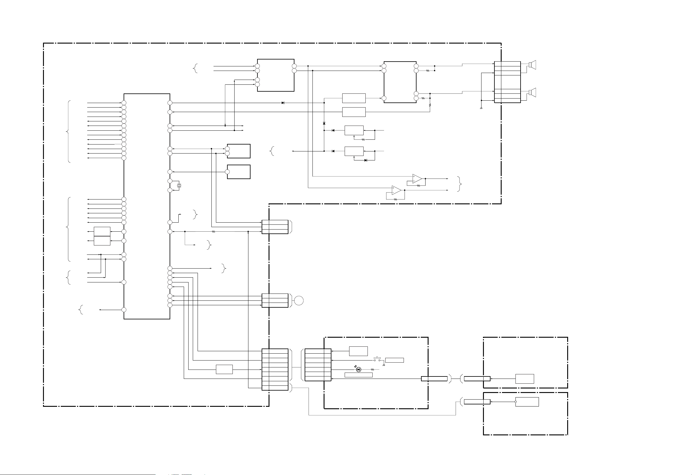
6-1. BLOCK DIAGRAM (1)
SECTION 6
DIAGRAMS
KP-XR432K90/XR432N90
RM-Y906K RM-Y906
TO
A
BOARD
TUNER
BLOCK
TO
A
BOARD
VIDEO
BLOCK
TO A
BOARD
PJED
BLOCK
STU AUMT
MTU AUMT
TO A
BOARD
TUNER
BLOCK
STUH
MTUH
STU AFT
MTU AFT
MONO
SAP
SAP IND
ST IND
AGC ATT
ANT SW1
ANT SW2
MICRO R
MICRO G
MICRO B
MICRO I
OSD YS
DISP YM
SBLK
MBLK
VP-BUFF
VP-BUFF
B INT
HP
HP
YUV MT
SWITCH
Q024
SWITCH
Q007
IC002
SYSTEM CONTROL
I-2HSYNC
1
I-HSYNC
2
SUBTU AFT
15
MAINTU AFT
16
O-MONO
17
O-SAP
18
I-SAPN
43
I-STEREN
60
O-2MUTE
61
O-MUTE
62
O-AGC ATT
51
ANT SW1
52
ANT SW2
53
32
O-R
33
O-G
34
O-B
35
O-I
36
O-OSDYS
37
O-DISPYM
O-SBLK
45
O-MBLK
46
7
I-HP
8
I-VP
I-BINTN
6
O-YUVMT
57
O-SPK MT
I-APROT
IO-SDAT
O-SCLK
IO-B DAT
O-B CLK
I-RESET
O-OSC
I-OSC
O-SIRCS
I-RMCN
O-GRAY
KEY
I-POWERN
O-TMRLED
MENU
I-OVP
I-OCP
O-RELAY
IC403
SDA
SCL
28
5
17
18
BOARD
TUNER
BLOCK
D/A CONVERTER
TO A
IN1
IN2
SCL
SDA
11
10
3
8
7
4
CN003
BCLK
B DAT
SIRCS
CN681
OVP
OCP
RELAY
OUT1
OUT2
P-MUTE
21
12
FOR
CHECK
G
TO G
BOARD
CN605
L/R MUTE
Q403, 404
PROTECT
Q408-411
OFF MUTE
Q402
ON MUTE
Q401
TO A
BOARD
TUNER
BLOCK
58
22
47
49
48
50
9
11
12
X001
16MHz
63
64
23
14
44
55
13
21
20
56
S OUT
ML OUT1
HR OUT1
TO A
BOARD
TUNER
BLOCK
RM IN
TO A
BOARD
TUNER
BLOCK
GRAY
IC004
EEPROM
5
B DAT
6
B CLK
4
RESET
IC001
RESET
TO A
BOARD
VIDEO
BLOCK
7
11
5
IN+(L)
IN+(R)
MUTE
+11V
STBY
+5V
3
2
IC404
IC406
L/R AMP
OUT(L)
IN-(L)
OUT(R)
IN-(R)
1
IC404
5
6
CN403
1
4
8
2
10
7
R OUT
L OUT
TO A
BOARD
TUNER
BLOCK
L
2
E
3
R
4
E
A
(AUDIO, SYSTEM CONTROL)
(1/6)
LED BUFF
Q006
CN002 CN1203
KEY
6
POWER
7
TIMER LED
8
MENU
9
SIRCS
2
KEY
POWER
TIMER LED
MENU
S1201-1206
3
4
5
6
CONTROL
SWITCHES
D1201
TIMER/STANDBY
POWER
STBY +5V
S1207
HA
(CONTROL SWITCHES)
– 25 –
CN1202
1 MENU KEY
CN1252
MENU KEY
CN1291
HB
(2/2)
(MENU SWITCHES)
S1251-1255
MENU
SWITCHES
OUT
D1291
REMOTE SENSOR
SIRCS
1
2
HC
(REMOTE SENSOR)
BLOCK DIAGRAM (2)
KP-XR432K90/XR432N90
RM-Y906K RM-Y906
ANT
SW
AUDIO
AUDIO
J1102
VIDEO 1
IN
S VIDEO
VIDEO
L(M
J1101
VIDEO 3
IN
S VIDEO
VIDEO
L(M
MAIN TUNER
SUB TUNER
ONO)
R
ONO)
R
TU151
DET OUT 2
DET OUT
AFT OUT
TU152
DET OUT
DE-EM
AFT OUT
CN004
ANT SW
ANT SW
L OUT
R OUT
ST IND
SAP IND
RF AGC
ODE
M
ONO
F M
UTE
M
SDA
SCL
OUT
UTE
M
SDA
SCL
1
2
3
1 2
3
1 2
IC1101
BUFFER
Q152
H.SEP
Q004
ITCH
SW
Q151
SDA
SCL
BUFFER
Q153
H.SEP
Q001
SDA
SCL
ITCH
SW
3
Q005
ITCH
SW
1
Q003
4
4
DET OUT
AFT OUT
ST IND
SAP IND
RF AGC
MODE
F MONO
TU AUM
M
L OUT1
M
HR OUT1
STUH
STUAFT
STUAUM
ANT SW
ANT SW
SYSTEM
T
T
SYSTEM CONTROL
1
2
TO A BOARD
CONTROL
BLOCK
TO A BOARD
BLOCK
63
62
64
52
54
60
59
61
12
10
14
11
19
17
21
15
16
18
8
9
MTV V
MTV L
TV R
M
ML OUT1
HR OUT1
STV V6
STV L6
STV R6
C1
Y1
-1
SSW
V1
L1
R1
C3
Y3
-3
SSW
V3
L3
R3
A/V SWITCH
M
AIN V OUT
SSW
SCL
SDA
SY OUT1
SC OUT1
C2
Y2
-2
V2
L2
R2
VIDEO BUFFER
41 41 23
5
3
7
1
2
4
33
34
56
58
SCL
SDA
Q1103,1104
Q1110
BUFFER
Q1701
10
7
9
5
3
1
UTE BUFFER
M
Q1122
CN1702
FR C IN
FR Y IN
FRONT SW
FR V IN
FR L IN
FR R IN
FL1701
UTE BUFFER
M
Q1117
FROM
SYSTEM
BLOCK
A BOARD
CONTROL
CN1253
FR C OUT
FR Y OUT
FRONT SW
FR V OUT
FR L OUT
FR R OUT
+11V
BUFFER
Q1702,1703
10
7
9
5
3
1
HB
(LINE IN 1)
IC1701
5V REG
I O
Q1119,1124
T
YUV M
UTE
P M
T
TU AUM
M
L OUT
R OUT
COMB FILTER
ADIN
CKIN
11
(1/2)
BUFFER
A BOARD
FROM
SYSTEM
BLOCK
IC1702
REG 5V
CONTROL
COUT
YOUT
3
1 2
BUFFER
FL1702
Q1704
BUFFER
Q1705
J1251
IN
ONO)
Q1118,1125
FL1703
AUDIO
BUFFER
25
VIDEO2
4
S VIDEO
VIDEO
L(M
R
BUFFER
Q1707,1708
BUFFER
Q1706,1709
43
C IN2
Y IN2
45
V BUFFER
Q1920
Y BUFFER
Q1914
Q1109
C OUT2
Y OUT2
37
39
BUFFER
Q1102
YUV SWITCH
DU IN
13
DV IN
3
1
DY IN
Q1108
IC1903
DVD SW
DVD SW
DVD SW
Y OUT
U OUT
V OUT
J1104
INH
V IN
U IN
Y IN
6
15
14
4
5
12
2
9
10
11
L
R
AUDIO OUT
(VAR/FIX)
TO BLOCK
1
DIAGRM(3)
J1106
Y
PB
PR
(2/6)
A
Y4
24
28
-4
SSW
L OUT
R OUT
38
40
TO A BOARD
SYSTEM
CONTROL
BLOCK
S OUT
RM
IN
SAVA CONT
Q1121
BUFFER
Q1114
AUDIO BUFFER
Q1112,1113
(TUNER, VIDEO, AUDIO IN/OUT)
SIRCS M
Q1111
IX
AUDIO BUFFER
Q1115,1116
BUFFER
Q1106,1107
Q1101
Q1105
J1105
J1103
CONTROL
S
OUT
VIDEO
L
R
AUDIO
ONIT OR
M
OUT
– 26 –
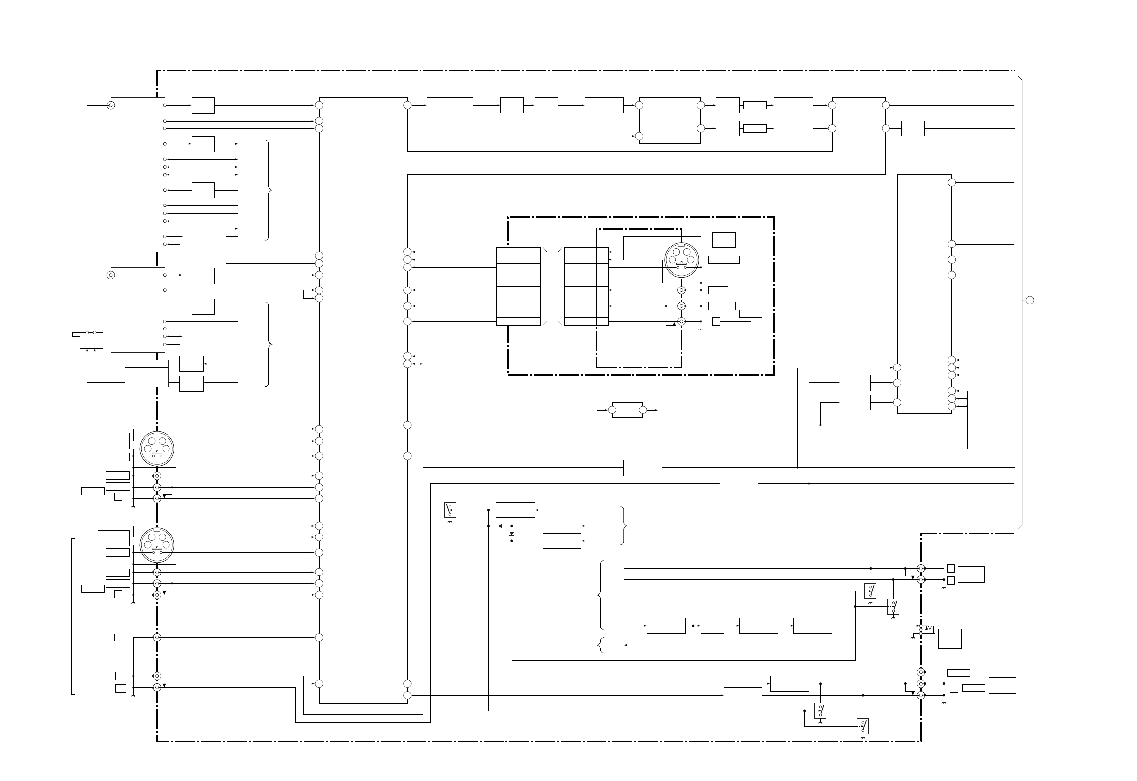
BLOCK DIAGRAM (3)
KP-XR432K90/XR432N90
RM-Y906K RM-Y906
TO BLOCK
DIAGRM(2)
IC1905
PIP PROCESSOR
M.VSYNC
17
SEL
Y OUT
U OUT
V OUT
S.VSYNC
S.HSYNC
M.HSYNC
12
8
9
7
19
20
18
Y BUFFER
Q1916
1
Y AMP
Q1917
BUFFER
Q1918
X1903
20.48MHz
SDA
SCL
YIN
28
UIN
30
VIN
32
XIN
3
XQ
4
SDA
21
SCL
22
SUB C BUFFER
Q1906
BUFFER
Q1915
BUFFER
Q1905
BUFFER
Q1907
BUFFER
Q1903
INV
Q1910,1911
SUB Y BUFFER
Q1904
BUFFER
1909
BUFFER
Q1908
SBLK
VP-BUFF
MBLK
SUB DECODER
11
RY IN
12
RU IN
13
RV IN
VTIM
14
SCP
16
HTIM
15
V OUT
20
U OUT
19
Y OUT
18
CIN
32
VSYNC
38
HSYNC
39
34
CVBS/Y IN
FROM A BOARD
SYSTEM CONTROL
BLOCK
IC1902
RY OUT
RU OUT
RV OUT
XNTSC
APC
CERA
SDA
SCL
CP IN
SYNC BUFFER
Q1913
8
7
6
X1902
26
3.58MHz
29
X1901
503.5KHz
1
37
SDA
36
SCL
10
IC1904
D/A CONVERTER
1
FULL
DVD
3
DVD SW2
MAIN YSM
HUE
COL
SDA
SCL
7
6
5
14
SDA
15
SCL
TO BLOCK
2
DIAGRM(4)
(3/6) (YUV CONTROLLER)
A
– 27 –

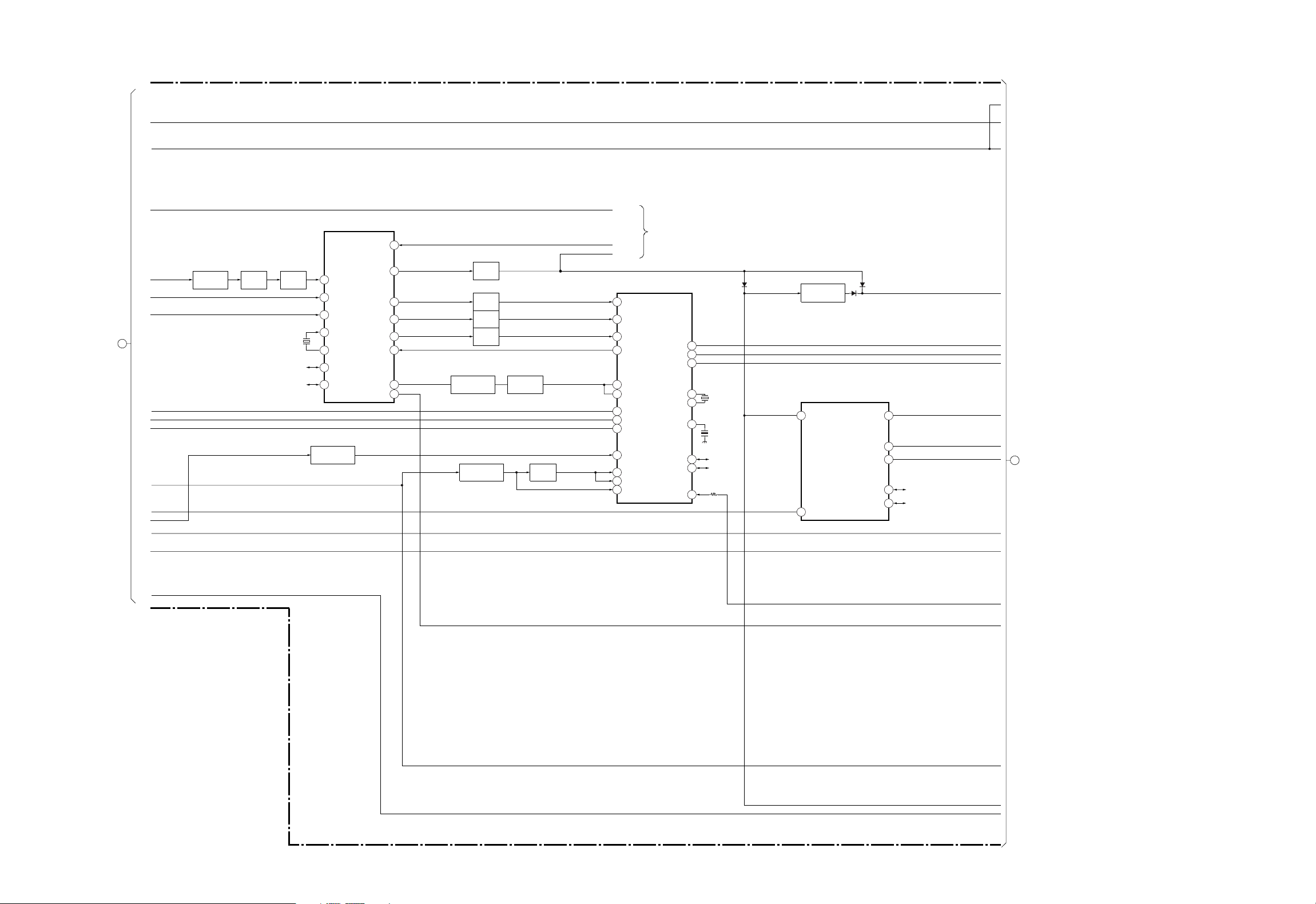
BLOCK DIAGRAM (4)
YVU CONTROLLER
TVIN
19 12
DVD Y
23
6
YUVSW
1
P Y
3
P B-Y
2
P R-Y
IC1901
TVOUT
YOUT
RYOUT
BYOUT
CLAMP
KP-XR432K90/XR432N90
RM-Y906K RM-Y906
Q232
Q304
Q229
CN204
9
R
7
G
5
B
1
1K
CN003
G
6
B
7
RGB MUTE
Q303
Q302
HP
Q301
+11V
10
4
5
6
8
2
CN801
ABL
HV PROT
PIN
HP
HD
V.BLK
H
FOR
CHECK
I
TO CG
BOARD
CN731
TO G
BOARD
CN1502
IC206
YCJ
CIN
IC301
INV
Q1912
8
9
10
5
PEEKING
Q262,227
BUFFER
Q305,306
BUFFER
Q228
LEVEL SHIFT
Q1901,1902
YUV SWITCH
1
3
2
7
GRAY
TO A BOARD
SYSTEM CONTROL
BLOCK
64
20
ROUT
63
YIN
EYIN
7
ERYIN
8
EBYIN
10
ABLIN/VCCOMP
AFCPIN/HOFF
BGP
55
GOUT
BOUT
IKIN
L2FIN
AFCFIL
E/WDRIVE
HDOUT
VTIM
24
26
27
COG AMP
44
45
28
43
37
41
31
Q225
AFC AMP
Q217
COG BUFFER
+9V
BUFFER
Q220
BUFFER
Q219
BUFFER
Q218
BUFFER
Q231
BUFFER
Q230
Q223
COG UNIT
Q205,224
FROM A BOARD
SYSTEM CONTROL BLOCK
TO BLOCK
DIAGRM(3)
Q011
Q018
SYNC BUFFER
Q221
BUFFER
Q002
BUFFER
Q008
BUFFER
Q009
BUFFER
Q010
BUFFER
Q014
BUFFER
Q015
BUFFER
Q016
BUFFER
0017
SCL
SDA
13
DLYSW
18
YSW
HUE
17
16
21
22
COLOR
DVD B-Y
DVD R-Y
IC1603
RESET
RST
BUFFER
Q1602
FROM A BOARD
SYSTEM CONTROL
BLOCK
IC1601
MAIN V CHIP/CC
7
VIDEO
5
HIN
45
SEN
SCL
SDA
14 15
14 15
5
HIN
SCL
SDA
SEN
4
7
VIDEO
IC1602
SUB V CHIP
R
G
B
BOX
2
MICRO R
MICRO G
MICRO B
MICRO I
DSD YS
DISP YM
18
2
3
Q021
Q022
Q023
17
SDA
SCL
BUFFER
Q1603
BUFFER
Q1601
FROM A BOARD
PJED
BLOCK
Q013
Q020
Q012
Q019
RE YM
RE YS
RE R
RE G
RE B
VSIN
51
HSIN
52
14
RIN
15
GIN
16
BIN
SCL
3
SDA
4
12
YM
13
YS
YUVSW
5
FSCOUT
57
VDRIVE-/VPROT
VDRIVE+
CERA
XTAL
34
35
X203
503.5KHz
46
X202
3.58MHz
59
54
VM
IC681
9V REG
+11V
I O
IC682
9V REG
I O
I
+11V
(4/6) (YC JUNGLE)
A
VM BUFFER
Q222
+9V
O
PIP 9V
5
6
6
CN202
V.DRIVE(-)
V.DRIVE(+)
CN203
VM
J
K
TO G
BOARD
CN501
TO CG
BOARD
CN1304
– 28 –
BLOCK DIAGRAM (5)
KP-XR432K90/XR432N90
RM-Y906K RM-Y906
LEFT
SENSOR
UPPER
SENSOR
LOWER
SENSOR
RIGHT
SENSOR
CN802
UPPER
LOWER
RIGHT
LEFT
IC804
PEAK HOLD
5
6
Q804
7
IC802
IV CONV
3
1
3
5
7
1
2
5
7
6
10
8
9
12
14
13
3
2
12
13
10
9
Q803
1
Q802
14
Q805
8
6
5
3
2
10
9
12
13
IC806
BUFF
7
1
SW
Q801
8
14
SCL
SDA
18
17
16
15
57
50
48
6
44
I AREGI D0
I AREGI D1
I AREGI D2
I AREGI D3
O AREG RST
MAIN SCL
MAIN SDA
BINT
I VPULSE
IC805
PJED-CPU
O DREGI MUTE
I EXLC
I HP
I DREG OVF
I DREG BSY
I DREG ACK
I VP
DREG SCL
O DREG SDA
I DREG SDA
O IIC SW
O DREGI RST
O NVM STOP
O KUMUPRT
RESET
39
7
26
27
28
8
49
47
46
58
61
62
59
55
9
PSCL
PSDA
A
(5/6)
(PJED-CPU)
TO A BOARD
VIDEO
BLOCK
TO A BOARD
SYSTEM CONTROL
BLOCK
RE-R
RE-G
RE-B
RE-YM
RE-YS
B INT
VP-BUFF
TO BLOCK
3
DIAGRM(6)
I OSC
12
X801
11
36
32
33
34
35
37
(2/6)
12MHz
YM OR
Q806
IC808
(5/6, 6/6)
3
10
13
VP
O OSC
O YS
OR
OG
OB
OI
O YM
IC808
4
HP
– 29 –

BLOCK DIAGRAM (6)
KP-XR432K90/XR432N90
RM-Y906K RM-Y906
TO BLOCK
DIAGRM(5)
IC803
DIGITAL REGI
HBLK IN
TEST5
PWM2
XOFDEF
XBUSY
XACKM
TEST4
VBLK IN
SCLS
SDAS
XRESET
XMUTE
XSTOP
XWC
SCLM
SDAM
RVOUT
RHOUT
BCLK
HBLK OUT
WCLK
GVOUT
GHOUT
BVOUT
BHOUT
CN801
(2/2)
1
REGI MUTE
D+5V
IC812
9
10
(3/4)
8
L
IC817
R DAC
RSI
LSI
CLK
LRCK
IC807
BV DAC
LSI
CLK
LRCK
ROUT
LOUT
LOUT
6
11
11
46
60
28
IC808
(4/6)
9
26
27
8
IC812
(2/4)
4
5
INV
6
14
15
16
13
15
16
13
IC816
IC824
RH-FILTER/BUFF
2
7
3
IC823
RV-FILTER/BUFF
2
7
3
DF
VP
D FOCUS
3
RH
10
RV
9
GH
7
5
GV
BH
3
BV
1
CN402
CN202(1)
VP
4
G DAC
IC822
RSI
LSI
CLK
LRCK
ROUT
LOUT
6
11
45
59
14
15
16
13
GH-FILTER/BUFF
2
7
3
IC815
B DAC
IC819
RSI
44
58
14
LSI
CLK
LRCK
ROUT
LOUT
6
11
15
16
13
BV-FILTER/BUFF
2
7
3
TO G
BOARD
CN1502
M
TO G
BOARD
CN651
N
TO G
BOARD
CN501
3
6
12
VCO OUT
PFD OUT
VCO IN
IC809
PLL
16MHz
FINA
FINB
4
5
INV(4/4)
11
IC812
12
13
15
+5V
30
IC808
(1/6, 3/6)
6
IC801
1
5
1
3
7
6
2
17
8
11
12
29
18
14
13
10
9
2
3
IC810
EEPROM
WP
VDD
A0
A1
A2
SCLM
SDAM
6
5
5
4
IC811
RESET
4
RST
7
8
1
2
3
3
RE-YM
RE-R
RE-G
RE-B
RE-YS
R OR
Q807
G OR
Q809
B OR
Q808
YS OR
Q813
Q811
ATT
Q812
ATT
IC814
OSD MIX
3
6
11
8
IC821
GV-FILTER/BUFF
2
7
1
2
4
5
13
12
9
10
HP
21
ROUT
GOUT
22
23
BOUT
25
YSOUT
DAOUT
38
DF
REGI OUT
+5V
IC818
CENT REF
2
3
1
A
(6/6)
(REGI CORRECTON)
3
IC820
BH-FILTER/BUFF
2
7
3
– 30 –
 Loading...