SONY KE-61MR1 Service Manual
SERVICE MANUAL
MBT-MR1 PDM-6100
KE-61MR1
Korea Model
MR1 CHASSIS
SPECIFICATIONS
Panel System Plasma Display panel
Display resolution Display resolution:
1365 pixels (horizontal) × 768 pixels (vertical)
Antenna 75 ohm external terminal for VHF/UHF
Television System NTSC
Channel Coverage VHF 2-13
UHF 14-69
CATV 1-125
Power Requirements 220V, 60 Hz
Inputs/Outputs
DVI-HDTV 1 terminal, 3.3V T.M.D.S., 50 ohms
Video (IN) 3 total (1 on front panel) 1 Vp-p, 75 ohms unbalanced, sync negative
S Video (IN) (1 on front panel) Y: 1 Vp-p, 75 ohms unbalanced, sync negative
Audio (IN) (1 on front panel) 500 mVrms (100% modulation)
Component Video Input 2 (Y, P
CONTROL S (OUT)
Variable/Fixed Audio (OUT) More than 408 m Vrms at the maximum volume
The DVI-HDTV input terminal is compliant with the EIA-861 standard and is not
intended for use with personal computers.
3 total
6 total
B
, PR) Y: 1.0 Vp-p, 75 ohms unbalanced, sync negative;
1
1
C: 0.286 Vp-p (Burst signal), 75 ohms
Impedance: 47 kilohm
B
: 0.7 Vp-p, 75 ohms
P
P
R
: 0.7 Vp-p, 75 ohms
setting (Variable)
More than 408 mVrms (Fixed)
Impedance (output): 2 kilohms
FLAT PANEL COLOR TV

Monitor/Fixed Audio (OUT) 1
Sub woofer (OUT) 1
RF Input
Converter
Screen Size (measured diagonally)
Speaker Output 15 W × 2
Dimensions (W × H × D)
Mass Display unit
Power Consumption
Supplied Accessories Remote Control RM-929Y
2
1
61 inches
PDM-6100
MBT-MR1
PDM-6100: 71 kg
Media receiver unit
MBT-MR1: 7.5 kg
In Use
In Standby
AAA (LR03) Batteries (2)
AC power code (2)
AC plug holder (1)
Display interface cable (1)
Antenna cable (1)
Cleaning cloth (1)
phono jack
1797 × 937 × 110 mm
430 × 105 × 360 mm
Display unit
Media receiver unit
Under 1.5 W
Design and specifications are subject to change without notice.
PDM-6100: 705 W
MBT-MR1: 36 W
KE-61MR1 (K) 2
SAFETY CHECK-OUT
After correcting the original service problem, perform the
following safety checks before releasing the set to the customer:
1. Check the area of your repair for unsoldered or poorly-soldered connections. Check the entire board surface for solder
splashes and bridges.
2. Check the interboard wiring to ensure that no wires are
“pinched” or contact high-wattage resistors.
3. Check that all control knobs, shields, covers, ground straps,
and mounting hardware have been replaced. Be absolutely
certain that you have replaced all the insulators.
4. Look for unauthorized replacement parts, particularly transistors, that were installed during a previous repair. Point them
out to the customer and recommend their replacement.
5. Look for parts which, though functioning, show obvious signs
of deterioration. Point them out to the customer and recommend their replacement.
6. Check the line cords for cracks and abrasion. Recommend
the replacement of any such line cord to the customer.
7. Check the antenna terminals, metal trim, “metallized” knobs,
screws, and all other exposed metal parts for AC Leakage.
Check leakage as described right.
LEAKAGE TEST
The AC leakage from any exposed metal part to earth ground
and from all exposed metal parts to any exposed metal part
having a return to chassis, must not exceed 0.5 mA (500
microamperes).
Leakage current can be measured by any one of three methods.
1. A commercial leakage tester, such as the Simpson 229 or RCA
WT-540A. Follow the manufacturers’ instructions to use these
instruments.
2. A battery-operated AC milliammeter. The Data Precision 245
digital multimeter is suitable for this job.
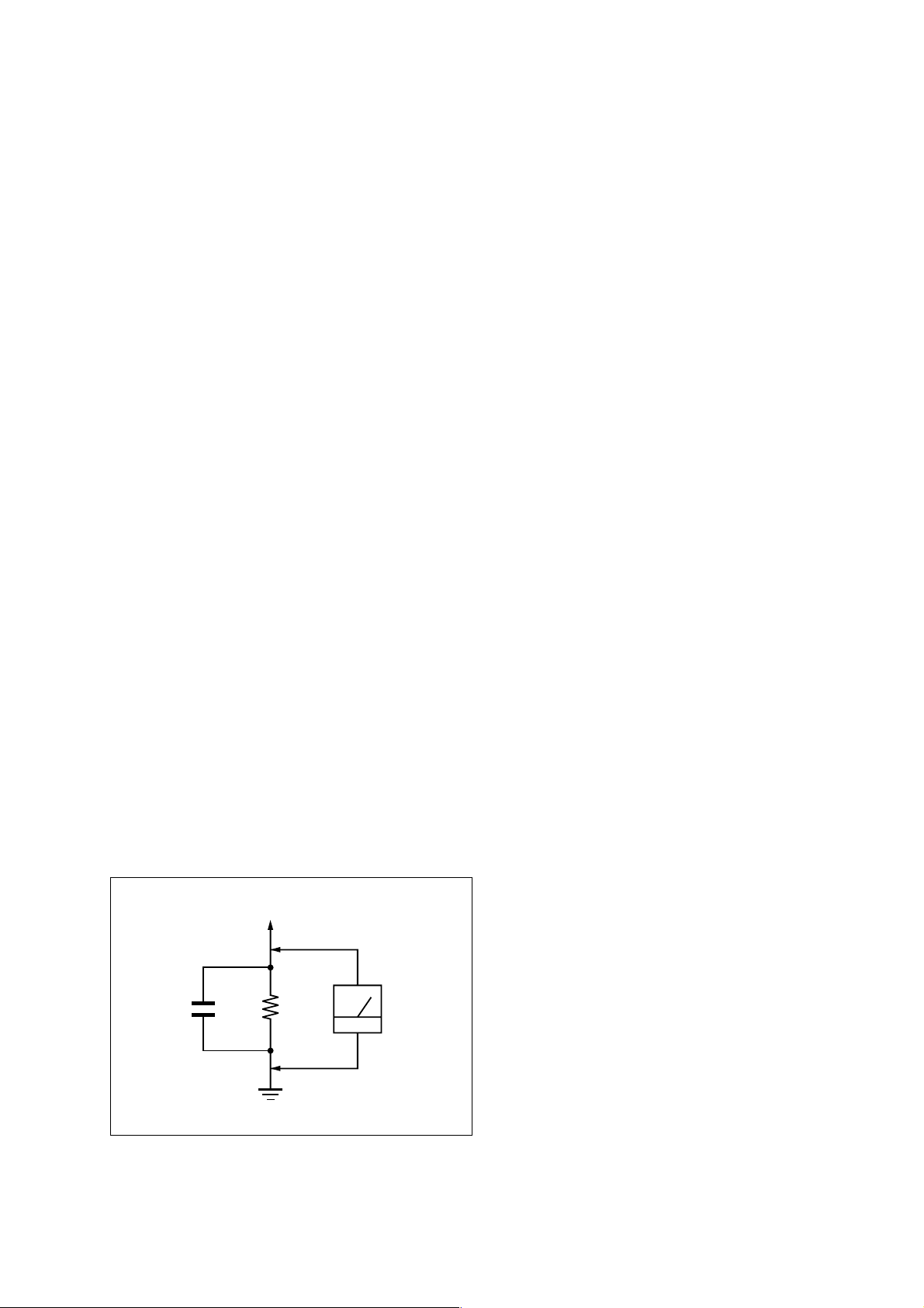
3. Measuring the voltage drop across a resistor by means of a
VOM or battery-operated AC voltmeter. The “limit” indication is 0.75 V, so analog meters must have an accurate lowvoltage scale. The Simpson 250 and Sanwa SH-63Trd are
examples of a passive VOMs that are suitable. Nearly all battery operated digital multimeters that have a 2 V AC range
are suitable. (See Fig. A)
WARNING!!
SAFETY-RELATED COMPONENT WARNING!!
COMPONENTS IDENTIFIED BY SHADING AND MARK
! ON THE SCHEMATIC DIAGRAMS, EXPLODED
VIEWS AND IN THE PARTS LIST ARE CRITICAL FOR
SAFE OPERATION. REPLACE THESE COMPONENTS
WITH SONY PARTS WHOSE PART NUMBERS APPEAR AS SHOWN IN THIS MANUAL OR IN SUPPLEMENTS PUBLISHED BY SONY. CIRCUIT ADJUSTMENTS THAT ARE CRITICAL FOR SAFE OPERATION
ARE IDENTIFIED IN THIS MANUAL. FOLLOW THESE
PROCEDURES WHENEVER CRITICAL COMPONENTS
ARE REPLACED OR IMPROPER OPERATION IS
SUSPECTED.
AVERTISSEMENT!!
ATTENTION AUX COMPOSANTS RELATIFS À LA
SÉCURITÉ!!
LES COMPOSANTS IDENTIFIÉS PAR UNE TRAME ET
UNE MARQUE ! SONT CRITIQUES POUR LA
SÉCURITÉ. NE LES REMPLACER QUE PAR UNE
PIÈCE PORTANT LE NUMÉRO SPECIFIÉ. LES
RÉGLAGES DE CIRCUIT DONT L’IMPORTANCE EST
CRITIQUE POUR LA SÉCURITÉ DU
FONCTIONNEMENT SONT IDENTIFIÉS DANS LE
PRÉSENT MANUEL. SUIVRE CES PROCÉDURES
LORS DE CHAQUE REMPLACEMENT DE
COMPOSANTS CRITIQUES, OU LORSQU’UN
MAUVAIS FONCTIONNEMENT EST SUSPECTÉ.
To Exposed Metal
Parts on Set
0.15 µF
1.5 k
Ω
Earth Ground
AC
Voltmeter
(0.75 V)
Fig. A. Using an AC voltmeter to check AC leakage.
KE-61MR1 (K) 3
DIAGNOSIS
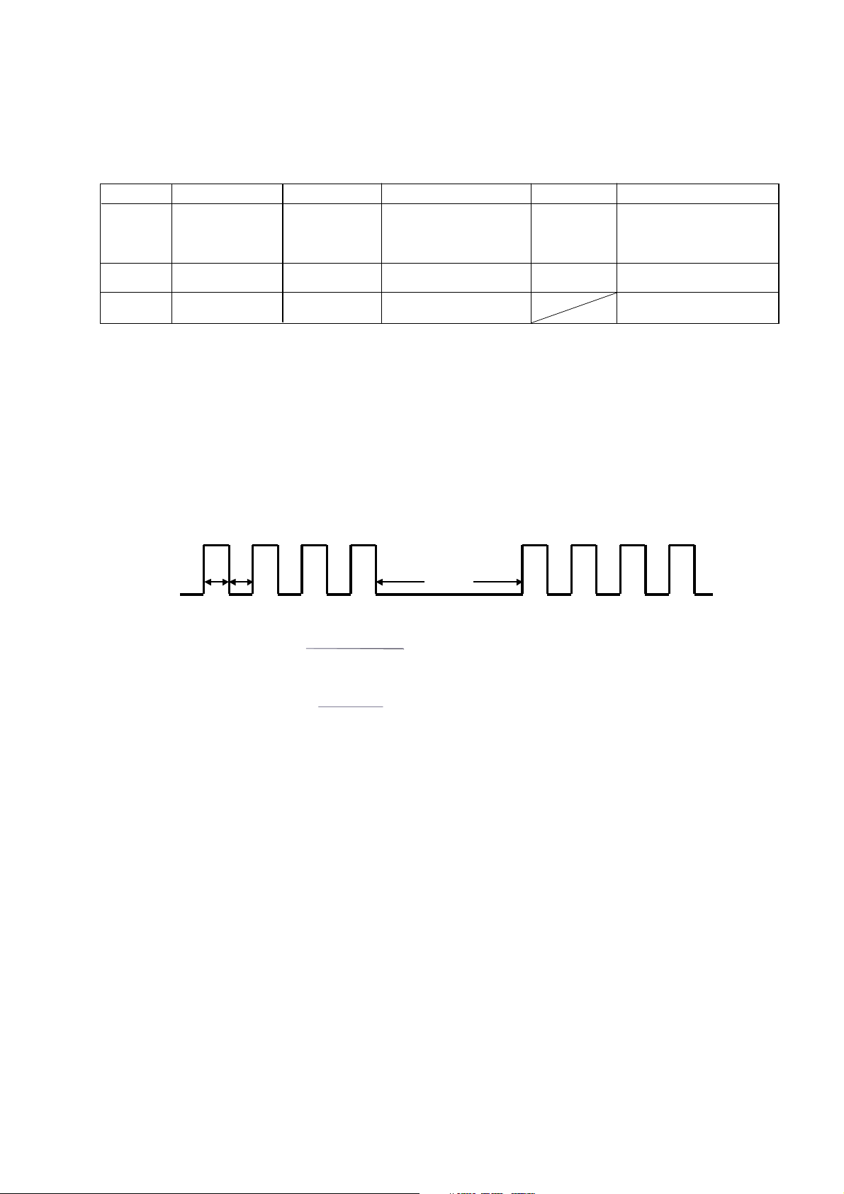
(Reliability Self Diagnostic Display Specifications for MEDIA RECEIVER)
The abnormal conditions are indicated by the following LED flashes.
Flash Count Error Display Name Error Description Oprating Detection Port
4 Fan Error Error detected for Detects Low when fan IC6200 pin #2
fan box function normally.
Detects High when Fan stops
abnormally
8 Digtal OVP OVP for DD Con- Detects High when normal. IC5210 pin #49
verter on DP board Detects Low when abnormal.
9 Panel Error Panel malfunction Detects during communication
detected with panel.
Repair part
• FAN
• FAN CONNECTOR
• SET 11V LINE
• SET 5V LINE
DP board
• Q1612, Q1613, Q1614
Panel Display Unit
1) *Operation count is based on WDT.
*For flashes, the Power/Standby LED flashes in red.
*The flash period is based on the reliability standard.
*A failure part can be expected by the number of times of blink of LED.
*When two failures occur, the failure item generated previously is detected.
*When failure occurs simultaneously, an item with little number of times of blink is detected.
*In other than
“Fan Error”, the unit is in standby state and blink LED at intervals of regulation.
In “Fan Error”, the unit is in a standby state after display for 1 minute about the message of “Fan problem –
Powering down”
• Timing of LED blink (example of 4 times blink)
ON
about 3s
OFF
every about 0.3s
In the following case, POWER LED of Media Receiver Box blinks at a fixed interval in ORANGE
2)
• When the cable which connects between Media Receiver Box and Panel Display has fallen out.
• When the AC code for Panel Display has fallen out.
In the following case, POWER LED of Panel Display
• When the cable which connects between Media Receiver Box and Panel Display has fallen out.
• When the AC code for Media Receiver Box has fallen out.
The example which judges whether it is failure
3)
• POWER LED of Media Receiver Box: Blink 9 times in RED, and of Panel Display blink,
and No picture or Power circuit does not work → Large possibility that Panel Display is out of order.
• When turn on Media Receiver Box, and NO LED of Box shine
→ Large possibility that Media Receiver Box is out of order.
When NO Blue LED of Box shine → Large possibility that Media Receiver Box is out of order.
•
Check SET5V or IIC line on H1 board.
• When turn on Media Receiver Box, and Fan does not work
→ Large possibility that Media Receiver Box is out of order
blinks at a fixed interval in ORANGE
KE-61MR1 (K) 4

TABLE OF CONTENTS
1. DISASSEMBLY ............................................ 1-1
1-1. DISPLAY UNIT (PDM-6100) ........................... 1-1
1-1-1. REAR COVER REMOVAL ......................... 1-1
1-1-2. G1 BOARD REMOVAL ............................... 1-2
1-1-3. F1, K2 AND P BOARDS REMOVAL ......... 1-2
1-1-4. G2 BOARD REMOVAL ............................... 1-3
1-1-5. SPEAKER BOX ASSY REMOVAL ............ 1-3
1-1-6. FILTER GLASS BRACKET ASSY
REMOVAL .................................................... 1-4
1-1-7. R1 BOARD REMOVAL ............................... 1-5
1-1-8. R2 BOARD REMOVAL ............................... 1-5
1-1-9. PLASMA DISPLAY PANEL ....................... 1-6
1-2. MEDIA RECEIVER UNIT (MBT-MR1) ......... 1-7
1-2-1. PANEL AND COVERS REMOVAL ........... 1-7
1-2-2. H1 BOARD REMOVAL ............................... 1-7
1-2-3. H4 BOARD REMOVAL ............................... 1-8
1-2-4. H3 BOARD REMOVAL ............................... 1-8
1-2-5. MS2 BOARD REMOVAL ............................ 1-9
1-2-6. H2 BOARD REMOVAL ............................... 1-9
1-2-7. A BOARD REMOVAL ................................. 1-10
1-2-8. B BLOCK ASSY REMOVAL ...................... 1-10
1-2-9. M, AD, AND AU BOARDS REMOVAL .... 1-11
1-2-10. AD AND AU BOARDS REMOVAL ........... 1-11
1-2-11. M BOARD REMOVAL ................................ 1-12
1-2-12. IFA BOARD REMOVAL ............................. 1-12
1-2-13. U1 BOARD REMOVAL ............................... 1-13
1-2-14. U2 BOARD REMOVAL ............................... 1-13
2. ADJUSTMENTS
2-1. VS, VD Voltage Adjustment (PDM-6100) ....... 2-1
2-1-1. Preparation for adjustment ............................. 2-1
2-1-2. Procedure for adjustment ............................... 2-1
2-2. White Balance Adjustment (PDM-6100) .......... 2-1
2-2-1. Measurement equipment ................................ 2-1
2-2-2. Measuring procedure ..................................... 2-1
4-4-2. MEDIA RECEIVER UNIT (MBT-MR1) ..... 4-30
(1) Schematic Diagrams of A Board ................... 4-30
(2) Schematic Diagrams of AD Board ................ 4-33
(3) Schematic Diagram of AU Board .................. 4-38
(4) Schematic Diagrams of BM1C Board ........... 4-40
(5) Schematic Diagrams of DICA Board ............ 4-43
(6) Schematic Diagram of DP Board .................. 4-49
(7) Schematic Diagram of H1 Board .................. 4-51
(8) Schematic Diagram of H2 Board .................. 4-53
(9) Schematic Diagram of H3 and H4 Boards .... 4-55
(10) Schematic Diagram of IFA Board ................. 4-56
(11) Schematic Diagrams of M Board .................. 4-58
(12) Schematic Diagram of MS2 Board ................ 4-64
(13) Schematic Diagram of U1 Board .................. 4-66
(14) Schematic Diagram of U2 Board .................. 4-68
4-5. SEMICONDUCTORS ....................................... 4-69
5. EXPLODED VIEWS ...................................... 5-1
5-1. DISPLAY UNIT-1 (PDM-6100) ....................... 5-2
5-2. DISPLAY UNIT-2 (PDM-6100) ....................... 5-3
5-3. MEDIA RECEIVER UNIT-1 (MBT-MR1) ...... 5-4
5-4. MEDIA RECEIVER UNIT-2 (MBT-MR1) ...... 5-6
5-5. PACKING MATERIALS FOR
DISPLAY UNIT (PDM-6100) ........................... 5-7
5-6. PACKING MATERIALS FOR
MEDIA RECEIVER UNIT (MBT-MR1) ......... 5-8
6. ELECTRICAL PARTS LIST ........................ 6-1
3. TROUBLESHOOTING .................................. 3-1
3-1. DISPLAY UNIT (PDM-6100) ........................... 3-1
3-2. MEDIA RECEIVER UNIT (MBT-MR1) ......... 3-1
4. DIAGRAMS ................................................... 4-1
4-1. BLOCK DIAGRAMS ........................................ 4-1
4-1-1. DISPLAY UNIT (PDM-6100) ...................... 4-1
4-1-2. MEDIA RECEIVER UNIT (MBT-MR1C) .. 4-5
4-2. FRAME DIAGRAM .......................................... 4-15
4-3. CIRCUIT BOARDS LOCATION ..................... 4-16
4-3-1. DISPLAY UNIT (PDM-6100) ...................... 4-16
4-3-2. MEDIA RECEIVER UNIT (MBT-MR1) ..... 4-16
4-4. SCHEMATIC DIAGRAMS AND
PRINTED WIRING BOARDS ........................ 4-16
4-4-1. DISPLAY UNIT (PDM-6100) ...................... 4-17
(1) Schematic Diagrams of F1 Board .................. 4-17
(2) Schematic Diagram of G1 Board .................. 4-18
(3) Schematic Diagram of G2 Board .................. 4-20
(4) Schematic Diagram of K2 Board .................. 4-22
(5) Schematic Diagram of R1 and R2 Boards .... 4-24
(6) Schematic Diagrams of P Board .................... 4-25
KE-61MR1 (K) 5
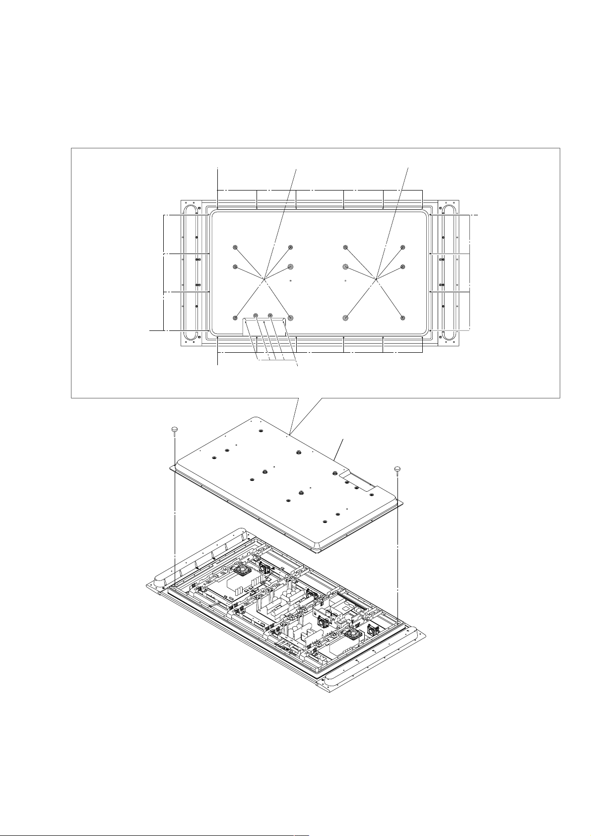
1-1. DISPLAY UNIT (PDM-6100)
1-1-1. REAR COVER REMOVAL
SECTION 1
DISASSEMBLY
1 Four screws
(+PSW 4x12)
1 Six screws
(+PSW 4x12)
1 Six screws
(+PSW 4x12)
2 Six screws
(+PSW 5x16)
3 Five screws
(+PSW 3x8)
4 Rear cover
2 Six screws
(+PSW 5x16)
1 Four screws
(+PSW 4x12)
KE-61MR1 (K) 1-1
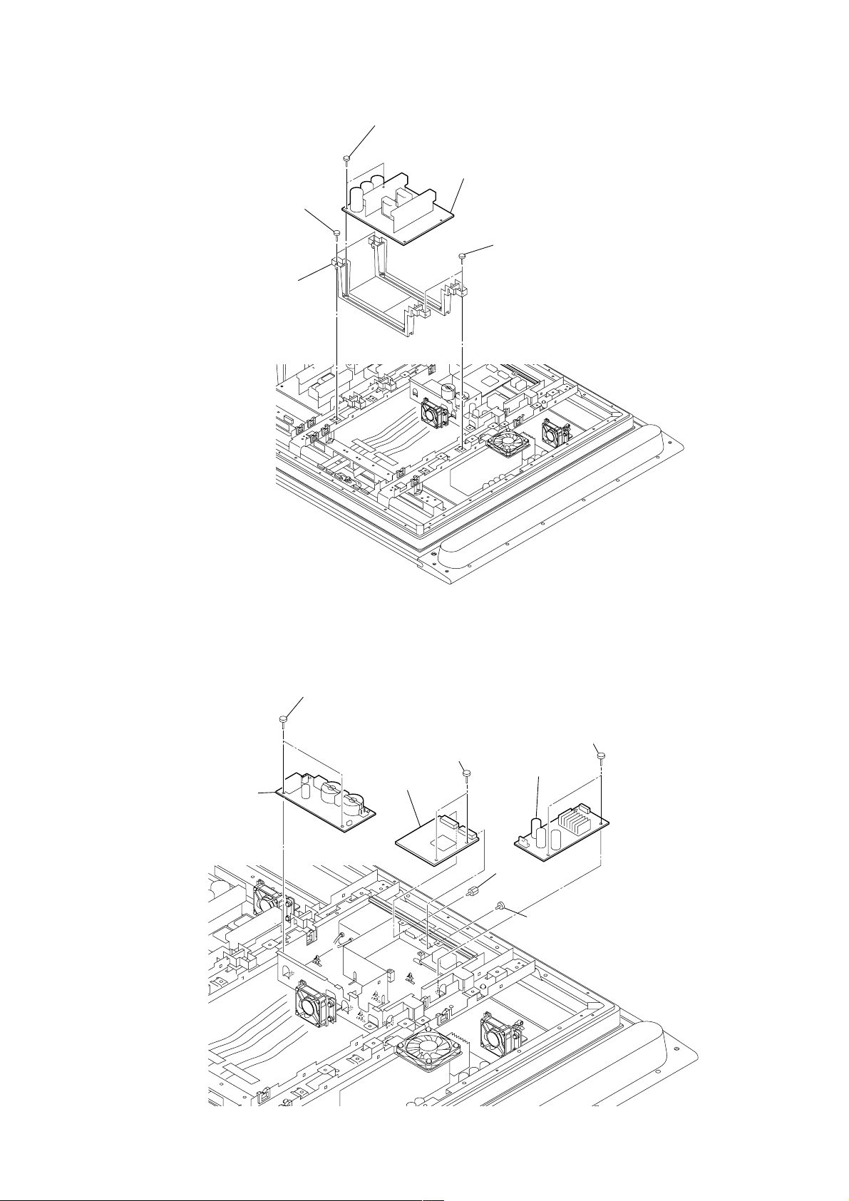
1-1-2. G1 BOARD REMOVAL
1 Two screws
(+PSW 4x12)
2 G1 bracket
3 Two screws
(+BVTP 3x12)
4 G1 board
1 Two screws
(+PSW 4x12)
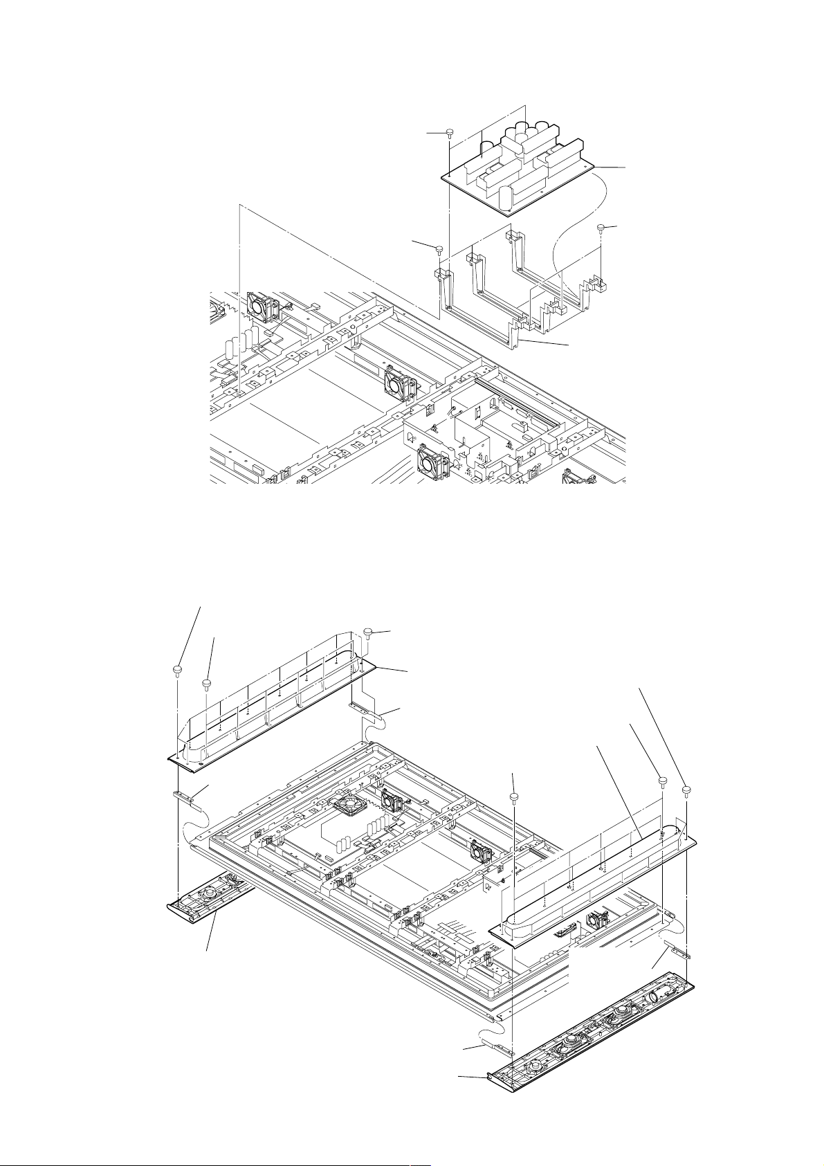
1-1-3. F1, K2 AND P BOARDS REMOVAL
1Two screws
(+PSW 3x8)
2 F1 board
5Two screws
(+PSW 3x8)
6 P board
7Two screws
(+PSW 3x8)
8 K2 board
3Two screws
(HEX)
4Two screws
(M2.6 S HEAD)
KE-61MR1 (K) 1-2
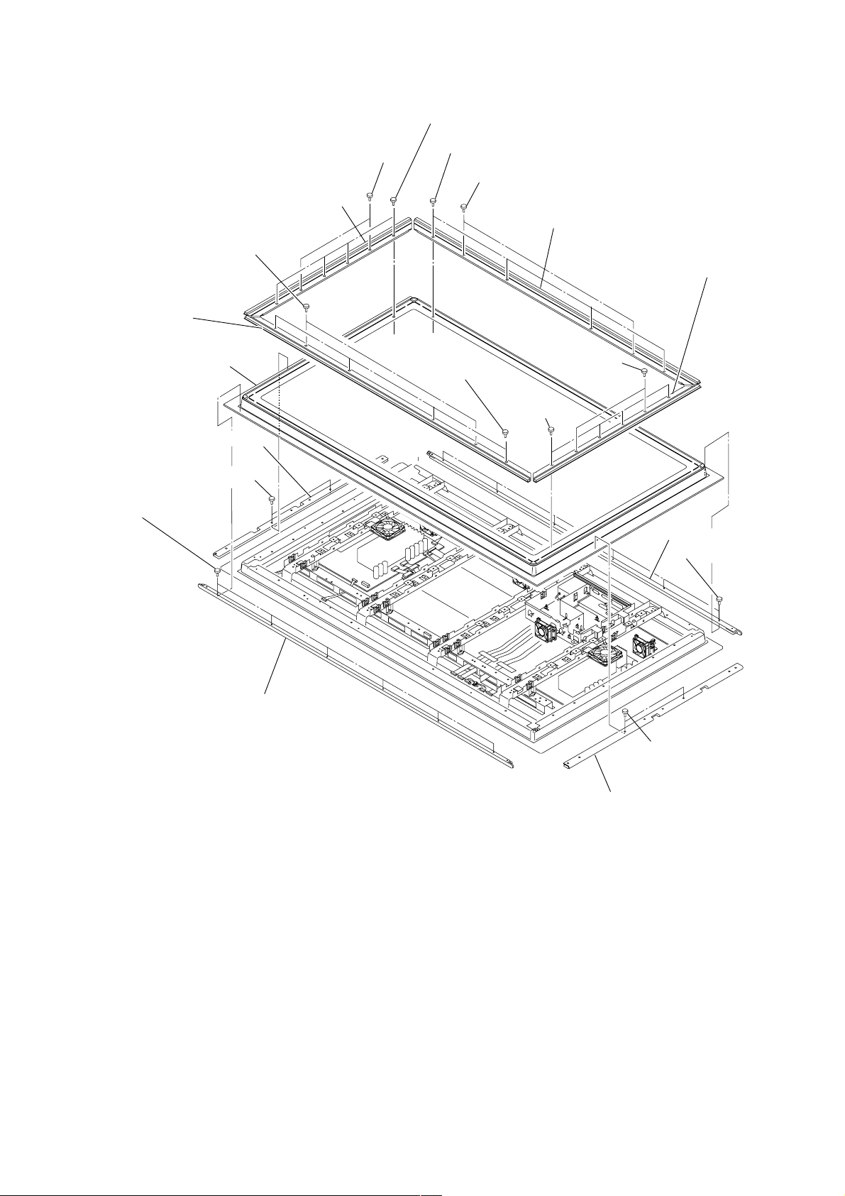
1-1-4. G2 BOARD REMOVAL
3 Three screws
(+BVTP 3x12)
4 G2 board
1 Three screws
(+PSW 4x12)
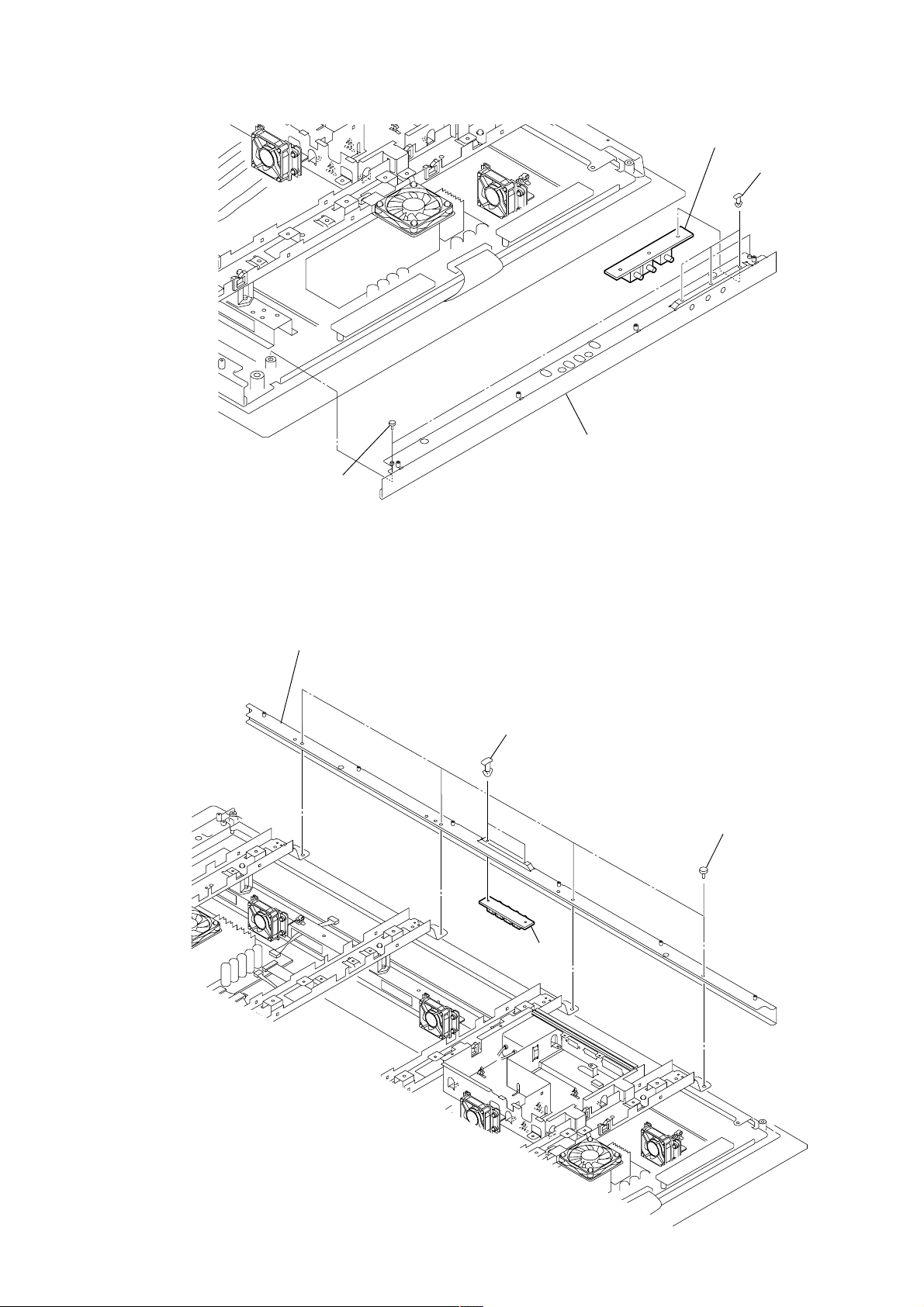
1-1-5. SPEAKER BOX ASSY REMOVAL
1 Ten screws
(+BTP 4x18)
3 Six screws
(+BVTP 4x16)
2 Four screws
(+PSW 4x10)
4 Speaker box (RL)
Speaker terminal (A)
1 Three screws
(+PSW 4x12)
2 G2 bracket
6 Ten screws
(+BTP 4x18)
7 Four screws
(+PSW 4x10)
9 Speaker box (RR)
Speaker
terminal (B)
5 Speaker box (L) assy
8 Six screws
(+BVTP 4x16)
Speaker
terminal (B)
Speaker terminal (A)
0 Speaker box (R) assy
KE-61MR1 (K) 1-3
1-1-6. FILTER GLASS BRACKET ASSY REMOVAL
1 Four screws (+BVTP 4x12)
2 Two screws
(+PSW 4x12)
3 Filter bracket assy (V)
5 Two screws
(+BVTP 4x12)
6 Filter bracket
assy (H)
!º Four screws (+PSW 4x12)
!¡ Two screws (+BVTP 4x12)
!™ Filter bracket assy (H)
9 Filter bracket assy (V)
@¡ Filter glass
bracket assy
@º Bar (V)
!ª Two fixed screws
!£ Six fixed screws
!¢ Bar (H) assy (UPPER)
4 Four screws
(+PSW 4x12)
7 Two screws
(+PSW 4x12)
8 Four screws
(+BVTP 4x12)
!§ Bar (H) assy
!∞ Six fixed screws
!¶ Two fixed screws
(+KTP 3x8)
!• Bar (V)
KE-61MR1 (K) 1-4
1-1-7. R1 BOARD REMOVAL
2 Filter bracket (H) block assy
1 Four screws
(+PSW 4x12)
3 PC board spacer
4 R2 board
1 Two screws
(+P 3x16)
4 R1 board
3 PC board spacer
2 Filter bracket (V) block assy
1-1-8. R2 BOARD REMOVAL
KE-61MR1 (K) 1-5
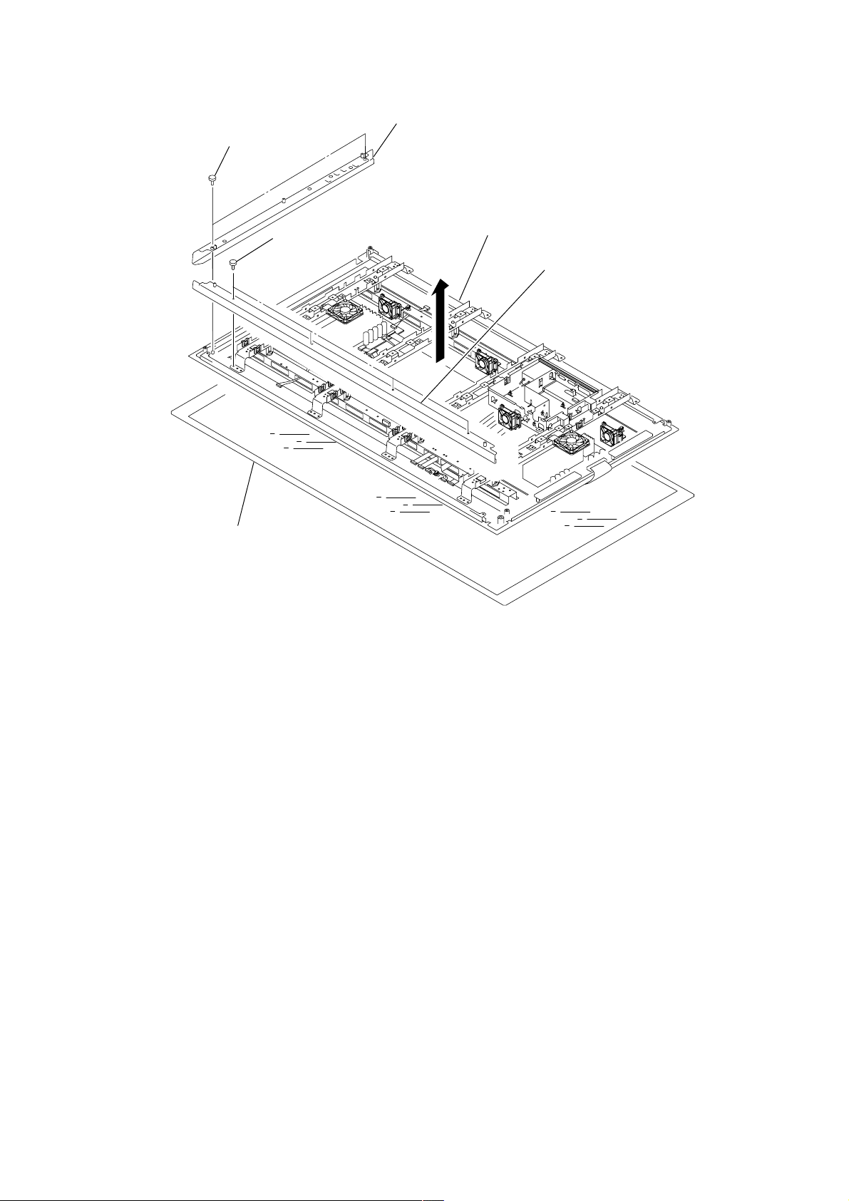
1-1-9. PLASMA DISPLAY PANEL
1 Two screws
(+P 3x16)
2 Filter bracket (V) block assy
3 Four screws (+PSW 4x12)
61 inch optical filter
5 61 inch plasma display panel
4 Filter bracket (H) block assy
KE-61MR1 (K) 1-6
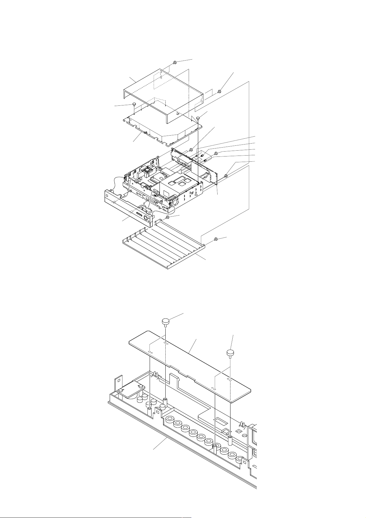
1-2. MEDIA RECEIVER UNIT (MBT-MR1)
1-2-1. PANEL AND COVERS REMOVAL
5 Top cover assy
1 Two screws
(+PSW 3X8)
3 Two screws
(+PSW 3X8)
7 Four screws
(precision)
8 Top chassis assy
9 Front panel assy
7 Eight screws
(precision)
2 Screw
(+PSW 3X8)
6 Bottom cover assy
3 Two screws
(+PSW 3X8)
!∞ Rear panel
4 Screw
(+PSW 3X8)
0 Two screws GRIP, M2.6 S'HEAD(EG)
!¡ Two screws (HEX)
!£ Four screws (+PSW 3X8)
!™ Two screws (HEX)
!¢ Two screws (+PSW 3X8)
1-2-2. H1 BOARD REMOVAL
Front panel
1 Two screws
(+BVTP 3X12)
2 H1 board
1 Two screws
(+BVTP 3X12)
KE-61MR1 (K) 1-7
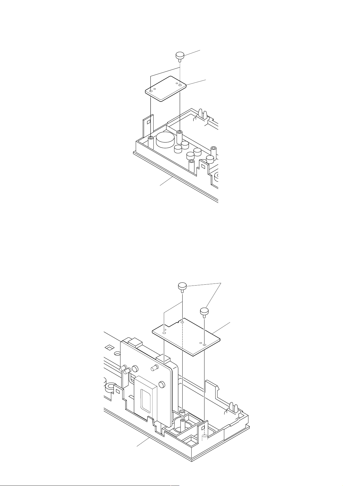
1-2-3. H4 BOARD REMOVAL
1 Two screws
(+BVTP 3X12)
2 H4 board
Front panel
1-2-4. H3 BOARD REMOVAL
1 Three screws
(+BVTP 3X12)
2 H3 board
Front panel
KE-61MR1 (K) 1-8
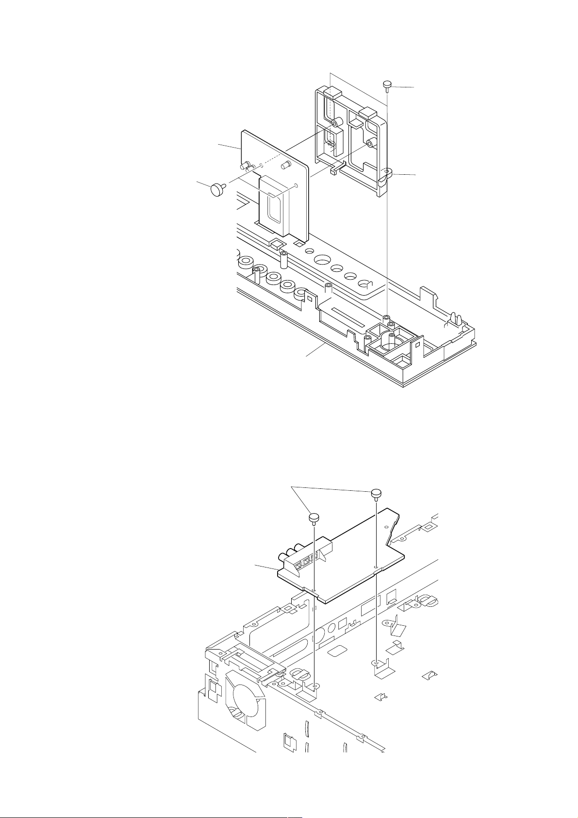
1-2-5. MS2 BOARD REMOVAL
4 MS2 board
1 Two screws
(+BVTP 3X12)
3 Two screws
(+BVTP 3X12)
1-2-6. H2 BOARD REMOVAL
2 MS bracket
Front panel
1 Two screws
(M 3X8),P,SW (+)
2 H2 board
KE-61MR1 (K) 1-9
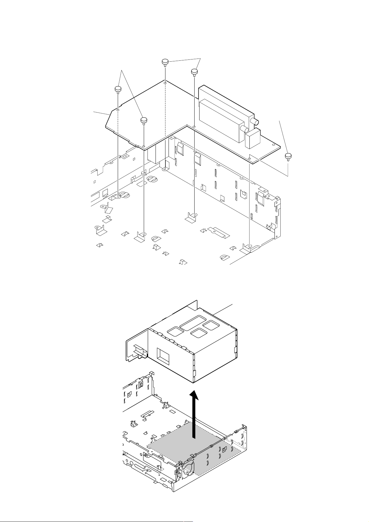
1-2-7. A BOARD REMOVAL
1 Two screws
(M 3X8),P,SW (+)
2 A board
1 Two screws
(M 3X8),P,SW (+)
1 Screw
(M 3X8),P,SW (+)
1-2-8. B BLOCK ASSY REMOVAL
1 B block assy
KE-61MR1 (K) 1-10
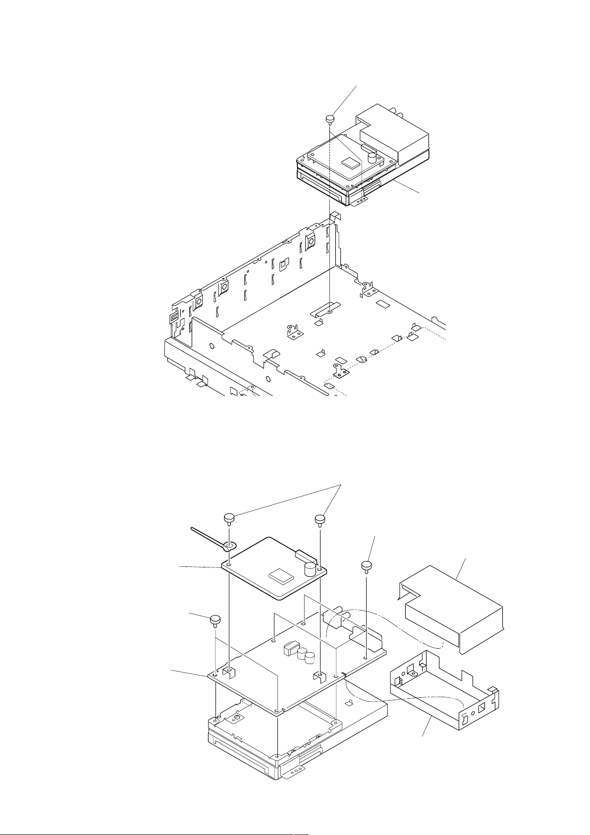
1-2-9. M, AD, AND AU BOARDS REMOVAL
1 Two screws
(+PSW 3x8)
2 Shield case
1-2-10. AD AND AU BOARDS REMOVAL
2 AU board
3 Two screws
(PSW 3x8)
4 AD board
1 Two screws
(PSW 3x8)
3 Four screws
(PSW 3x8)
Shield upper
Shield main
KE-61MR1 (K) 1-11
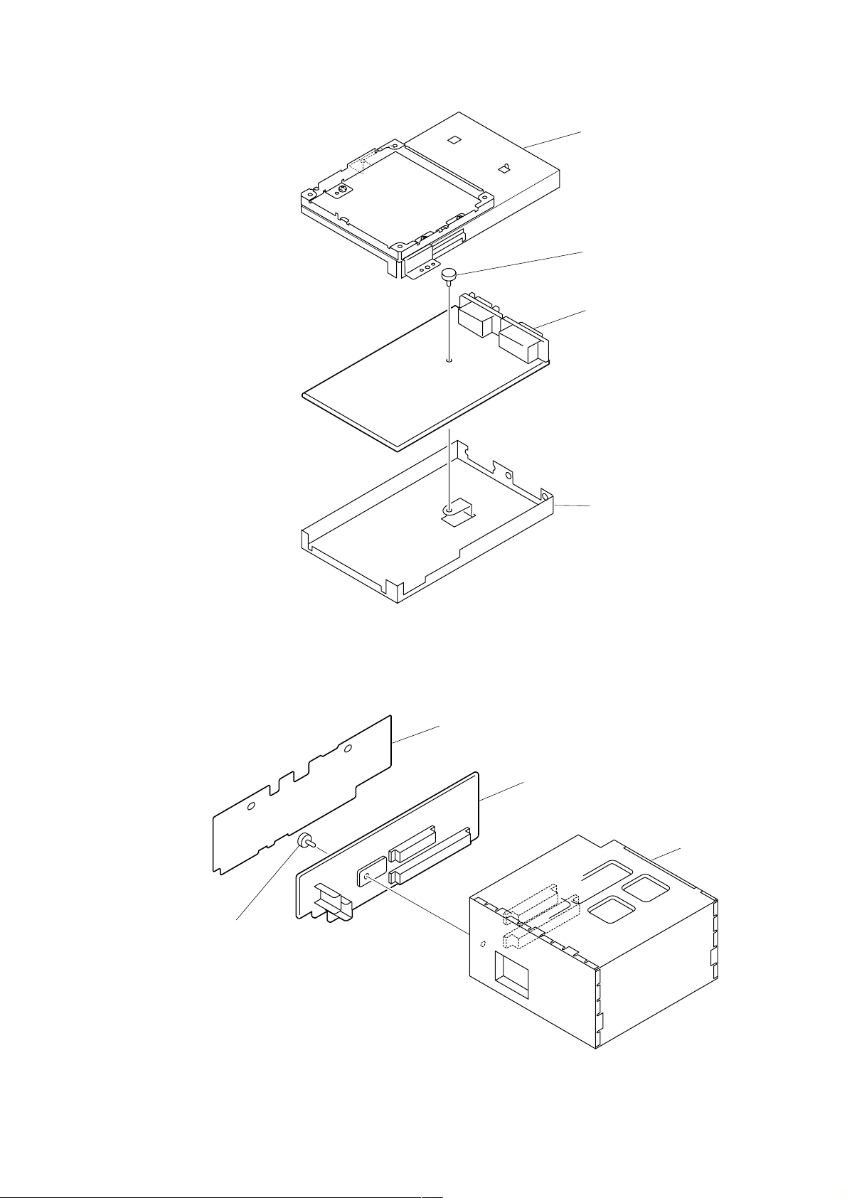
1-2-11. M BOARD REMOVAL
1 Shield case (upper)
2 Screw
(+PSW 3x8)
3 M board
1-2-12. IFA BOARD REMOVAL
2 Screw
(+PSW 3x8)
Shield case (main)
1 IF shield sheet
3 IFA board
B block assy
KE-61MR1 (K) 1-12
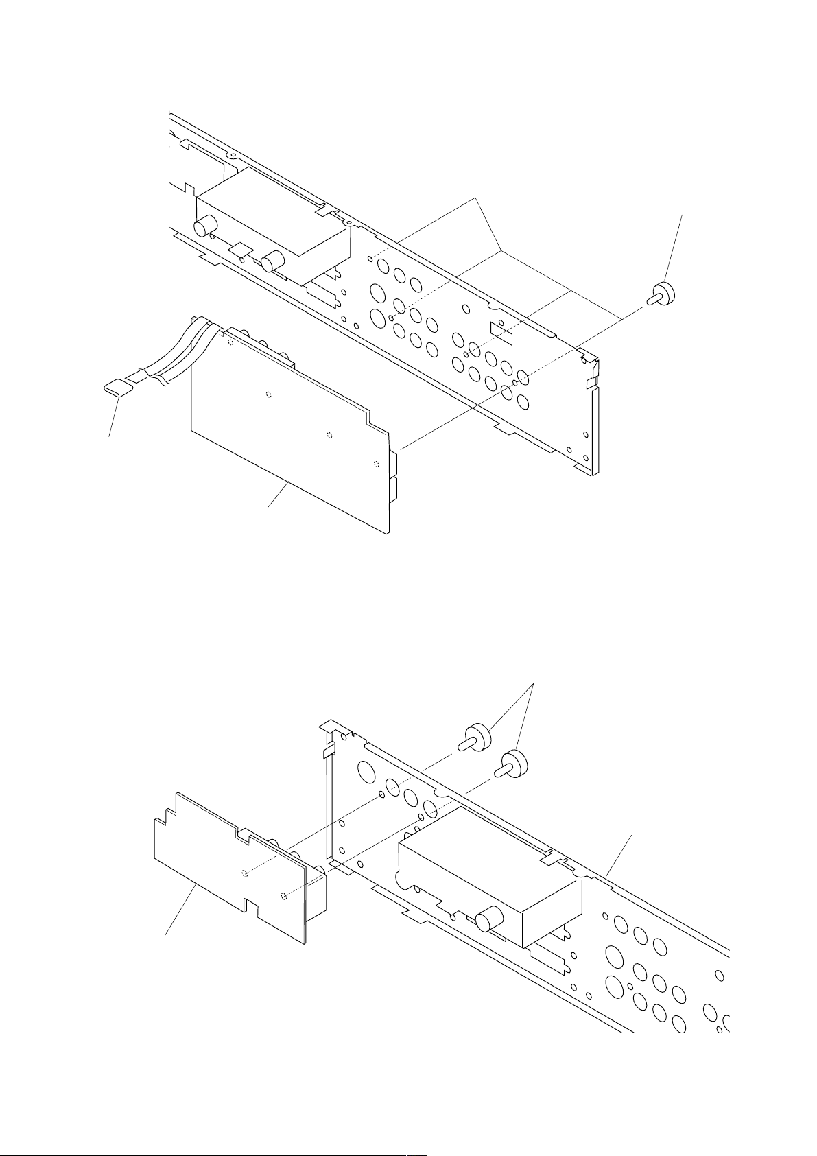
1-2-13. U1 BOARD REMOVAL
3 Core (FPC)
1 Four screws
(+BVTP 3x12)
2 U1 board
1-2-14. U2 BOARD REMOVAL
1 Two screws
(+BVTP 3x12)
Rear panel
2 U2 board
KE-61MR1 (K) 1-13E
SECTION 2
ADJUSTMENTS
2-1. VS, VD Voltage Adjustment (PDM-6100)
2-1-1. Preparation for adjustment
1. Slide the DIP switch (S3201) No. 8 of P board to on position
with no silkscreen mark r.
2. Connect a digital voltmeter to the following terminals of G
board.
VS voltage=G board TP1701 (VS)-TP1502 (GND)
VD voltage=G board TP1501 (VD)-TP1502 (GND)
3. Connect a AC cord in DISPLAY UNIT.
4. Perform the adjustment in 10 seconds after connecting the
cord.
2-1-2. Procedure for adjustment
1. Slide the DIP switch (S3201) No. 7 of P board to on position
with no silkscreen mark r.
2. Confirm the lighting of SONY LOGO LED.
3. Adjust the VS voltage to the following voltage value.
VS voltage of proper value for each model.
Ex.) VS proper value=185V thru 185.6V at 185V.
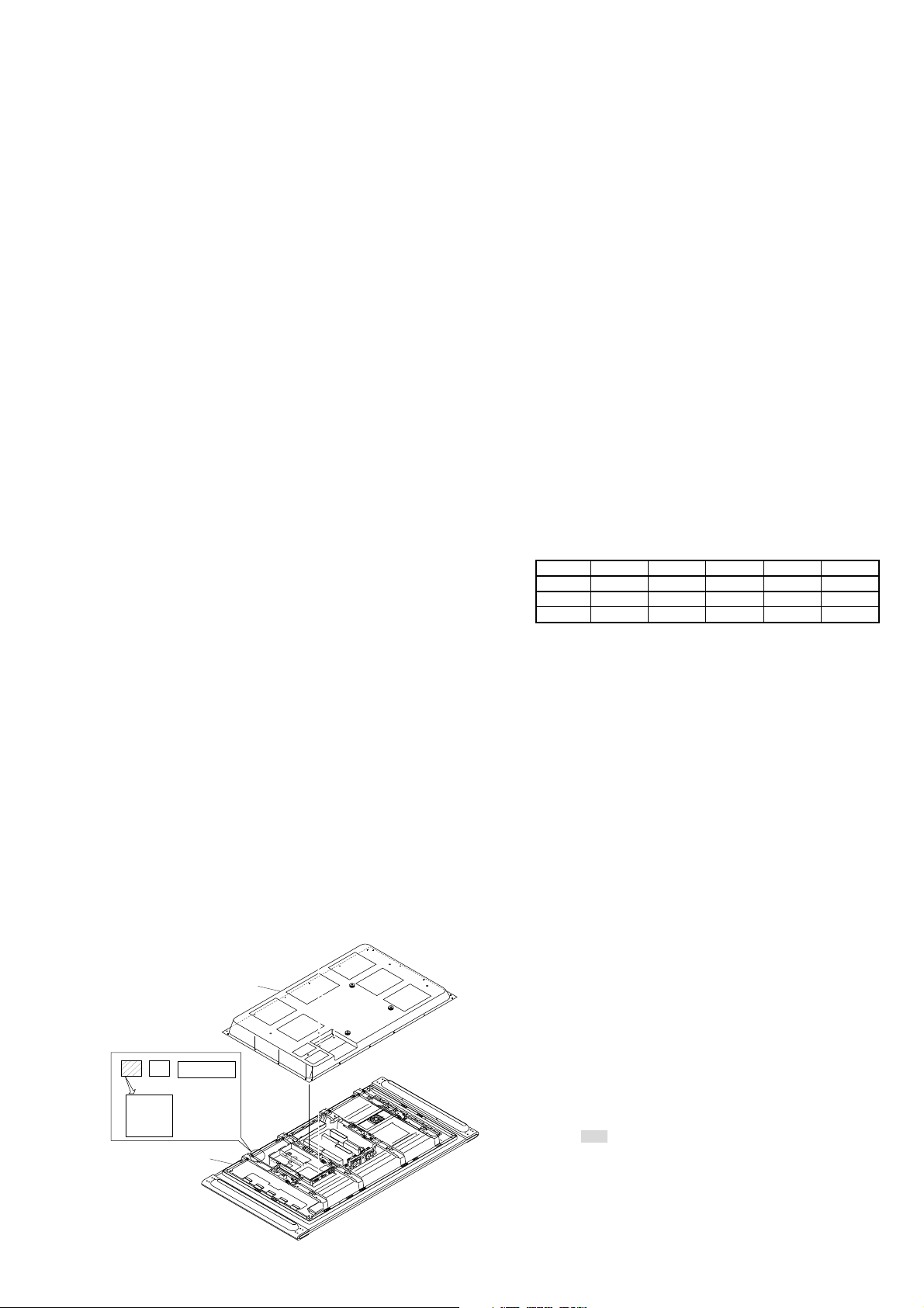
(Check the proper value with a seal on upper left of panel
unit. Refer to right Fig.)
4. Adjust the VD voltage to the following voltage value.
VD voltage ±0.3V of proper value for each model.
Ex.) VD proper value=64.7V thru 65.3V at 65.0V.
(Check the proper value with a seal on upper left of panel
unit. Refer to right Fig.)
5. Check a Fan rotation.
6. Slide the DIP Switch (S3201) No. 7 of P board to the off
position with the silkscreen mark r.
7. Slide the DIP Switch (S3201) No. 8 of P board to the off
position with the silkscreen mark r.
8. Disconnect an AC cord of DISPLAY UNIT.
9. Reconnect the AC cord in one second.
10. Assure that “POWER ON/STANDBY” LEDs is flashing
amber.
+6V
–0V
<SEAL POSITION>
Rear cover assy
2-2. White Balance Adjustment (PDM-6100)
2-2-1. Measurement equipment
1. Color analyzer (CA-100 manufactured by MINOLTA)
2. Signal generator (ASTRO DESIGN VG-828D)
2-2-2. Measuring procedure
1. Dab the W/B adjustment jig (CA-100) at the glass face of the
panel.
2. Connect the Signal generator (VG-828D) to the DVI
terminal.
3. Input All-white signal and set the picture mode to
DYNAMIC.
4. Select”PNLCTRL” in the service mode menu and set “0
WBNO” at “0”
5. Select “SCNR” “SCNB” of “PDPWB” in the service mode
menu, and then adjust following W/B standardized values
of 6500K, 8000K, 9300K, 10000K and 13550K to following
values of X/Y.
W/B standardized values:
6500K+8MPCD
W/B
0.3133 ± 0.003
X
0.3297 ± 0.003
Y
6. After adjusting the values, at the values of the “SCNR” or
“SCNB” exceeding 128 (initialize value).
1) Reset a lager value of the “SCNR” or “SCNB” at 128.
2) Set the White Balances with the last of items and “SCNG”
to the X/Y values above.
7. After the above step, when these item are nonqualified
following conditions, set the largest one at 128 and readjust
the White Balance with the last two item.
1) No one of “SCNR”, “SCNB” and “SCNG” exceeding 128
2) Confirm the item value 128 at least one item
8. As a result above, input the sequential number of value to the
“SCNR”, “SCNB” and “SCNG”.
9. Repeat the same step 5 thru 8 for the W/B 1 thru 4 after
setting the “0 WBNO” at each W/B number.
10. Input following signals from the Signal generator (VG828D).
1) All-white signal (255/255) input
Y (luminance)=45cd/m
2) 1/25Window (255/255) input
Y (luminance)=45cd/m
0
8000K+8MPCD
1
0.2944 ± 0.003
0.3100 ± 0.003
2
or more
2
or more
9300K+8MPCD
2
0.2838 ± 0.003
0.2981 ± 0.003
10000K
3
0.2806 ± 0.003
0.2883 ± 0.003
13550K
4
0.2684 ± 0.003
0.2700 ± 0.003
SERIAL No.
301201440
Vd=65V
Vs=193.4V
CODE AA-01
BAR CODE SEAL
Panel unit
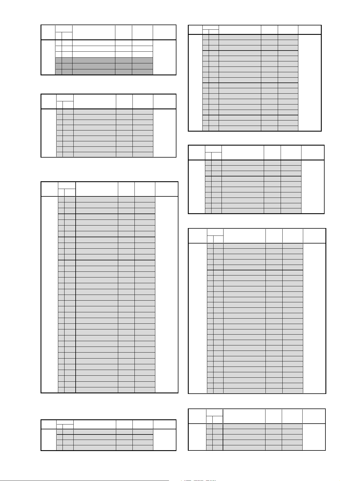
• Service mode lists
Caution: 1. Setting functions of Display section are displayed
with yellow OSD.
2. Be careful not to set DATA in the yellow-covered
OSD menu. The setting will be memorized.
3.
items are not required adjustment or are banned
adjustment.
KE-61MR1 (K) 2-1
Category
Category
Item Function Data range Initialize value Device Name
No. Name (Slave Address)
PDPPLE 00 PLE0
01 PLE1
02 PLE2
03 PLE3
04 PLE4
05 PLE5
06 PLE6
07 PLE7
08 PLE8
09 PLE9
10 PLEA
11 LMAX
12 LMIN
13 GAIN
14 OFFS
15 SAFL
16 LIFH
17 SPLE
Category
Item Function Data range Initialize value Device Name
No. Name (Slave Address)
PDPDYPIC 00 TLVL
01 TFVL
02 THLD
03 PLVL
04 PFIL
05 PHLD
06 PGUP
07 PGDN
08 PHIS
09 PGAN
Category
Item Function Data range Initialize value Device Name
No. Name (Slave Address)
PDPOTHER 00 DTMD
01 VIDT
02 CODE
03 ORBT
04 FV
Item Function Data range Initialize value Device Name
No. Name (Slave Address)
PDPWB 00 SCNR
01 SCNG
02 SCNB
03 SBRR
04 SBRG
05 SBRB
Sub contrast RED gain
Sub contrast GREEN gain
Sub contrast BLUE gain
Sub brightness RED
Sub brightness GREEN
Sub brightness BLUE
0-255 128 CXD9738R
0-255 128
0-255 128
0-255 128(Fix)
0-255 128(Fix)
0-255 128(fix)
Category
PDPSHAP 00 CRMD
Category
PDPGMMA 00 GMMA
Category
PDPSTAT 00 SRNU
Item Function Data range Initialize value Device Name
No. Name (Slave Address)
01 HTAP
02 VTAP
03 AGCM
04 EDDL
05 EDGA
06 EDNM
07 EDDE
08 DHVS
Item Function Data range Initialize value Device Name
No. Name (Slave Address)
01 GMR0
02 GMR1
03 GMR2
04 GMR3
05 GMR4
06 GMR5
07 GMR6
08 GMR7
09 GMR8
10 GMR9
11 GMRA
12 GMG0
13 GMG1
14 GMG2
15 GMG3
16 GMG4
17 GMG5
18 GMG6
19 GMG7
20 GMG8
21 GMG9
22 GMGA
23 GMB0
24 GMB1
25 GMB2
26 GMB3
27 GMB4
28 GMB5
29 GMB6
30 GMB7
31 GMB8
32 GMB9
33 GMBA
Item Function Data range Initialize value Device Name
No. Name (Slave Address)
01 SRNL
02 ROMV
03 OPTM
Category
PDPDISPOS 00 VAR1
Item Function Data range Initialize value Device Name
No. Name (Slave Address)
01 VAR2
02 HTLL
03 HTLM
04 VTLL
05 VTLM
06 HS1L
07 VS1M
08 HE1L
09 HE1M
10 VS1L
11 VS1M
12 VE1L
13 VE1M
14 HS2L
15 HS2M
16 HE2L
17 HE2M
18 VS2L
19 VS2M
20 VE2L
21 VE2M
22 V1SH
23 V1DT
24 V1AP
25 V2SH
26 V2DT
27 V2AP
KE-61MR1 (K) 2-2E
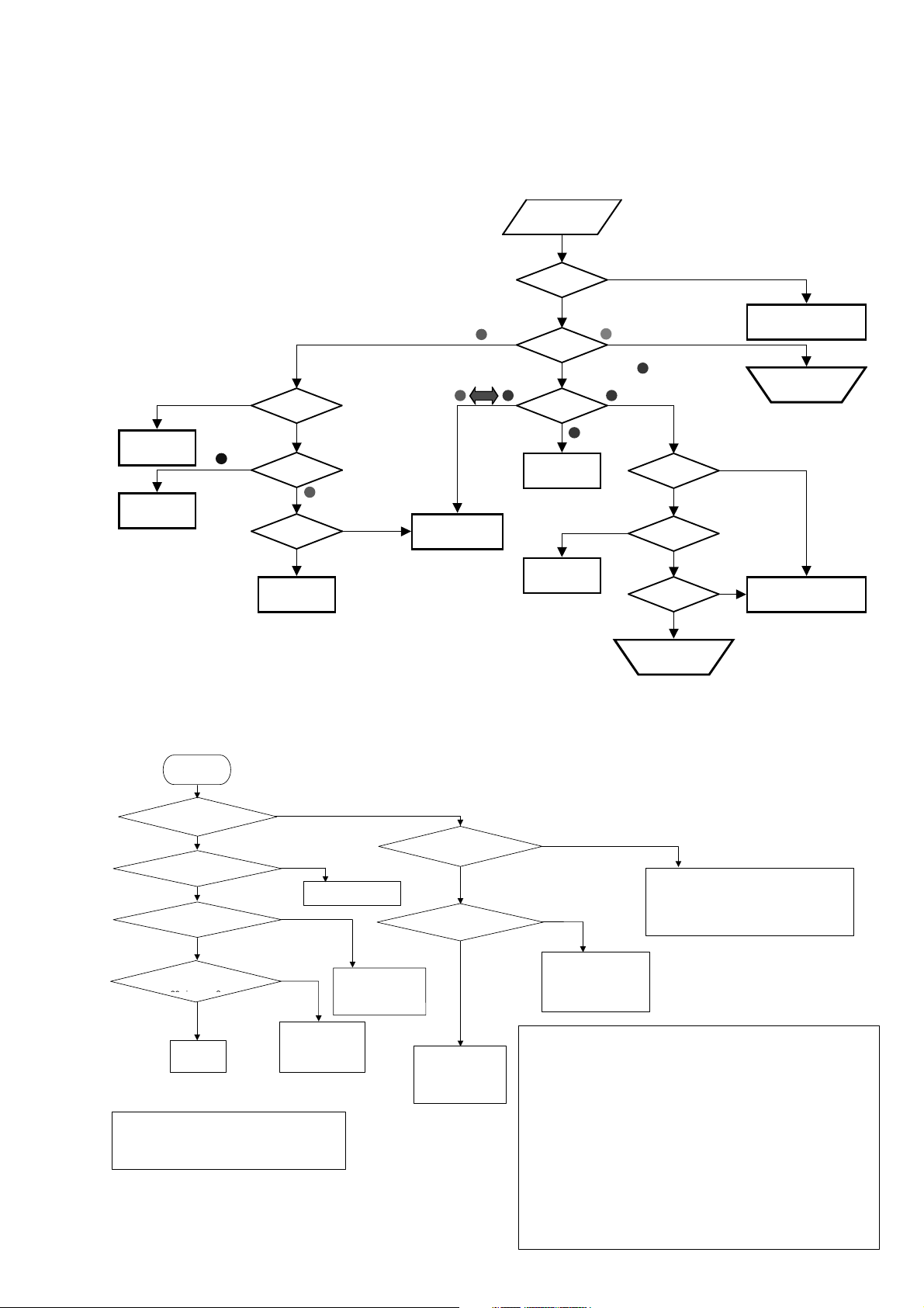
3-1. DISPLAY UNIT (PDM-6100)
(IC5002) on M
SECTION 3
TROUBLESHOOTING
No image
appears.
Abnormal
Box LED?
All is normal.
Box failure
Lights.
LED display
Image erasure
mode
Lights.
NO: No light
Priming?
emission
YES: Light emission
Panel module
P board failure
3-2. MEDIA RECEIVER UNIT (MBT-MR1)
Lights.
Blinks alternately.
failure
Just after
start?
YES: Not appear at all.
LED display
BOX LED Blinks nine times.
LED display
Blinks six times.
G board failure
Fan or
circuit failure
NO: Appears for a few seconds.
Encrypted authentication
Blinks.
Blinks four times.
Just after
error of box or display
YES
start?
NO
NO
Fan rotation?
YES
OK
Installation
environment?
Temperature sensor
NG
Environment
improvement
Check of cable
connection
or circuit failure
Sound not output
from speaker
No sound from Both
speakers for all input
YES
"MONITOR OUT"
output ?
YES
"SUBWOOFER"
output ?
YES
Display Signal Out
(Black) 26pin output?
YES
Possibility
•
Cable defect
•
Panel failure
Note)
If the condition of small or no sound occurs for only one speaker,
perform the balance adjustment beforehand as follows:
MENU → AUDIO→BALANCE → ADJUST
NO
NO
•
Check CXA2069Qs
(IC4001, IC4303) on AD
NO
(try to turn up volume)
(make sure the input signal
is under 200Hz)
NO
(DC signal only)
•
Check AK4114
(IC5003) on M
•
Check
SN65LVDS1050
(IC5101) on M
•
Check input of
NJW1149
(IC4703) on AU
•
Check AK4524
No sound from one
speaker for all input
YES
"SURROUND" ON
output?
YES
•
Check CXA2069Q
(IC4001, IC4303) on AD
•
Check input of
NJW1149
(IC4703) on AU
NO
NO
•
Check output of NJW1149
(IC4703) on AU
•
Check output of AK4524
(IC5002) on M
•
Panel failure
•
Check of AK4524 (IC5002) on M
No problem when around 3MHz of rectangular wave (3.3Vpp) is output from the 13-pin
SDTO. (The rectangular wave changes depending on the audio signal.)
For the analog system, check the inputs (2 and 3pins) and the outputs (25 through 28pins). The
outputs of these terminals change depending on the volume adjustments.
•
Check of AK4114 (IC5003) on M
No problem when around 3MHz of rectangular wave (3.3Vpp) is output for the JL5003 [SPDIF].
(The rectangular wave changes depending on the audio signal.)
Check that 48kHz of rectangular wave (3.3Vpp) is supplied to the 24-pin LRCK.
(Supply source: AK4524)
Check that 3.072MHz of rectangular wave (3.3Vpp) is supplied to the 26-pin BICK.
(Supply source: AK4524)
•
Check of Display Signal Out (Black) 26pin
The output signal level is about 3.3Vpp when the Display Signal Out terminals are not connected to
the Display unit.
If the signals, SPDIF+/- and UART_O+/-, are output, no problem for the sending end.
(When the Diplay Signal Out terminals are connected to the Display unit via display interface cable,
the signal level is about 350mVpp since the signal is terminated at Display unit.)
For receiving ends ( SIRCS input and UART input) the check can only be performed when the
Display Signal.
Out terminals are connected to the diplay unit.
Check the source of input signal whichsound does not
come.
•
Check TUNER
•
Check INPUT TERMINAL
•
Check CXA2069Q
(IC4001, IC4303) on AD
KE-61MR1 (K) 3-1E
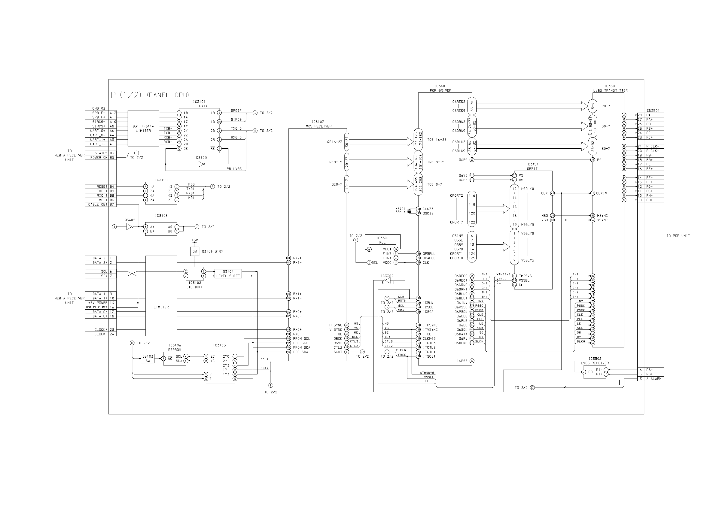
4-1. BLOCK DIAGRAMS
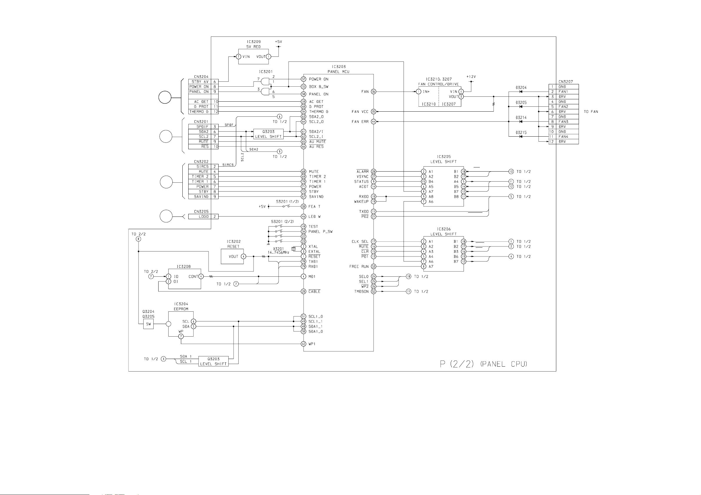
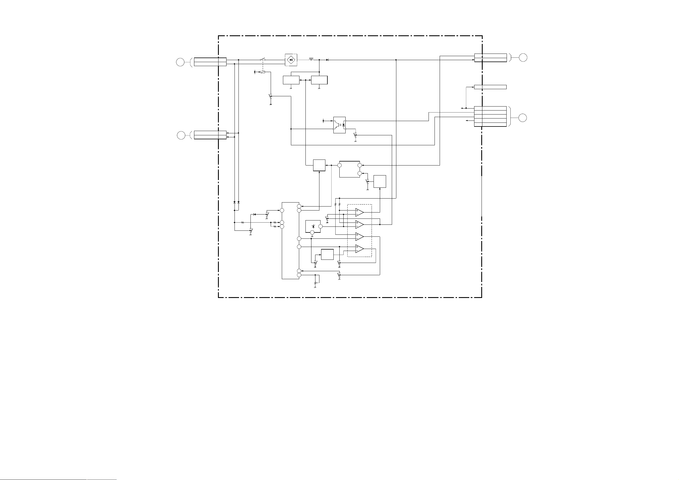
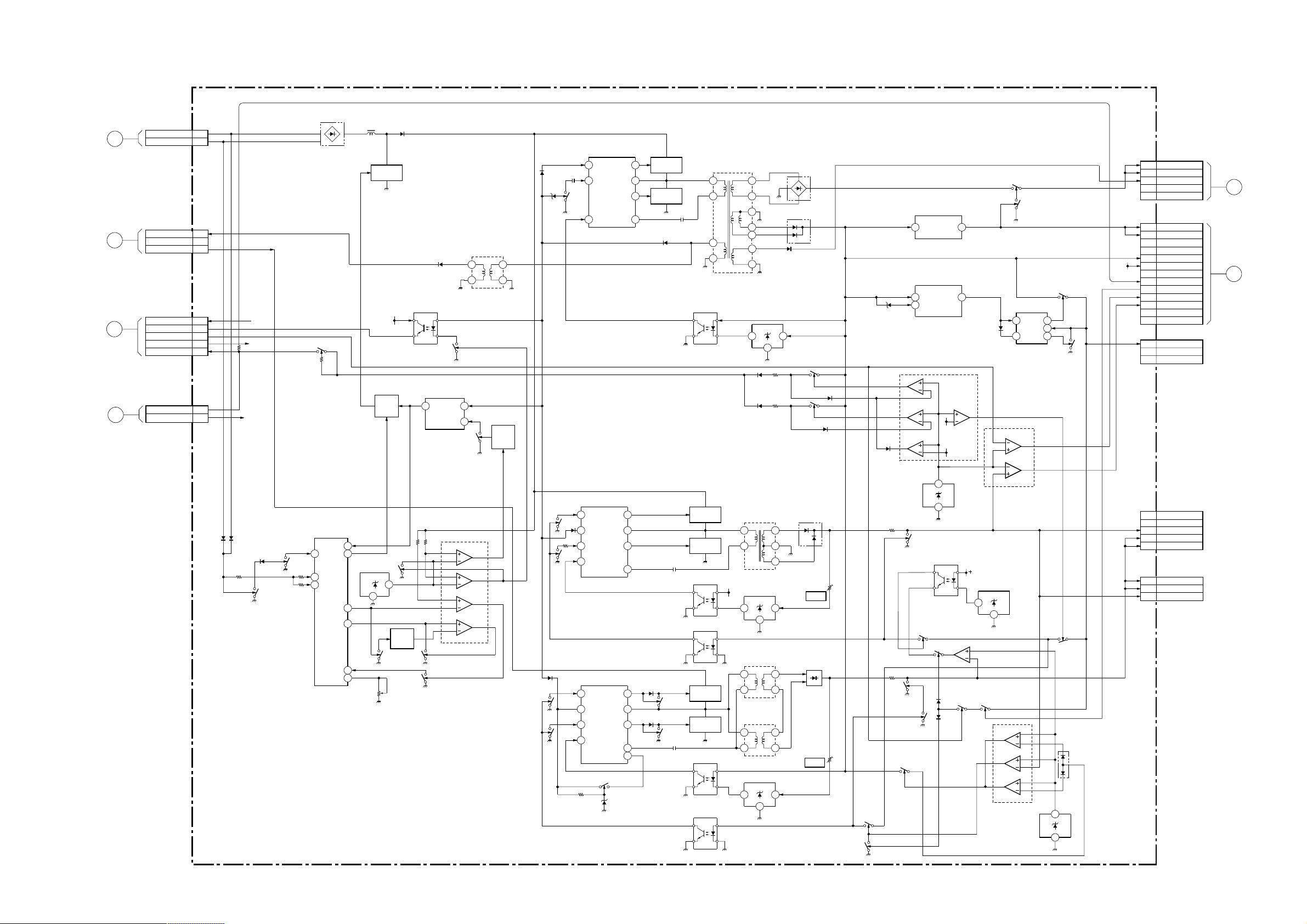
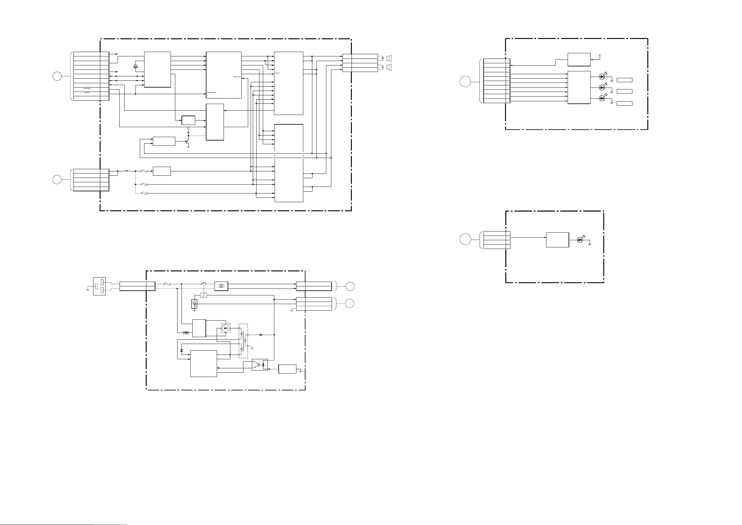
4-1-1. DISPLAY UNIT (PDM-6100)
SECTION 4
DIAGRAMS
LVDS
CN3101
DDC
DDC
WP
SEL1
SEL0
CABLE DETECT
D3104-3107
SELECTOR
1Y0
PDF0
CLX
VSO
ALM
KE-61MR1 (K) 4-1
TO G2 BOARD
TO K2 BOARD
TO R2 BOARD
CN751
A
CN1007
B
CN3301
C
TO R1 BOARD
CN701
D
ALM
VSO
RXD0
TXD0
PD LVDS
MUTE
CLR
FIELD
FREE
KE-61MR1 (K) 4-2
H
TO F1 BOARD
CN603
L
TO G2 BOARD
CN1004
CN2005
AC
AC
CN2001
AC
AC
D2004
RECT
Q2008
CONVERTER
L2001-2003 D2016
Q2009
CONVERTER
+12V
Q2003
+12V
Q2005
DRIVE
PH2202
ISOLATER
Q2202
SW
IC2003
REG
31
OUT VCC
2
CTL
Q2018
OVP
Q2019
Q2020
LATCH
+12V
+6V
+12V
RY2001
Q2015
RELAY
DRIVE
2
1
1
3
CN2004
18V_2
41380V_2
CN2002
1 12V
CN2003
12V
1
PFC_SW1
2
PFC_SW2
3
STBY 6V
5
LATCH(NC)
6
K
TO G2 BOARD
CN1001
J
TO G2 BOARD
CN1002
D2002
D2009
D2008
Q2001
RESET
Q2004
SS RES
10
6
8
IC2001
DRIVE
ENA
IAC
VRMS
VCC
OUT
VREF
IERR
SS
VFB
15
16
9
3
13
11
IC2004
Q2011
SS RES
RV2001
VREF
2
3
Q2012
LVP
Q2013
Q2017
SS
Q2006
SS
Q2024
OVP
IC2002
SS/PROTECT
12
14
13
3
1
2
5
7
6
10
8
9
G
1(POWER)
KE-61MR1 (K) 4-3
L
TO G1 BOARD
CN2001
K
TO G1 BOARD
CN2004
J
TO G1 BOARD
CN2003
I
TO F1 BOARD
CN604
CN1004
AC
AC
CN1001
18V-2
GND
CN1002
12
PPC-SW1
PPC-SW2
STBY5V
CN1005
POWER
STBY5V
2
1
1
2
3380V_2
1
2
3
5
6LATCH
2
3
D1002
G2
12V
6V
6V
D1009
Q1004
Q1001
RESET
SS RES
D1008
(POWER)
D1004
RECT
Q1014,1016
LATCH
IC1001
DRIVE
VCC
10
ENA
OUT
IAC
6
8
VRMS
VREF
IERR
SS
VFB
L1001-1003 D1016
Q1009
CONVERTER
+12V
Q1003
Q1005
DRIVE
15
16
IC1004
VREF
2
9
3
Q1011
SS RES
13
11
RV1001
3
D1208
PH1202
ISOLATER
IC1003
+12V
Q1012
LVP
Q1013
Q1017
SS
Q1006
REG
31
OUT VCC
CTL
IC1002
SS/PROTECT
12
13
3
2
5
6
10
9
SS
Q1024
OVP
Q1202
SW
2
Q1018
OVP
7
7
14
1
7
8
T1202
PIT
2
4
Q1019
Q1020
LATCH
D1601
Q1601
SW
Q1602
SS RES
D1204
D1201
Q1401
SW
Q1404
SW
Q1201
SS
IC1201
DRIVER
VC18
7SS
VG(L) 12
OCP 9
F/B2
IC1401
DRIVER
VSENSE
VG(H)116
VC1
SS
F/B2
IC1601
DRIVER
VSENCE
VS815
VC1
VG(L)712
SS
2 F/B
OCP
VC2
Q1603
REGULATOR
D1602
VS 15
20V
158 VS
127 VG(L)
9OCP
161 VG(H)
9
10
16VG(H)
Q1203
CONVERTER
Q1204
CONVERTER
D1208
Q1604
Q1605
1
2
3
4
PH1201
ISOLATER
4
3
Q1405
CONVERTER
Q1406
CONVERTER
PH1401
ISOLATER
PH1402
ISOLATER
Q1606
CONVERTER
Q1607
CONVERTER
PH1601
ISOLATER
PH1602
ISOLATER
1
2
T1201
PIT
+12V
13
12
9
7
6
13
12
2
D1313
D1314
T1401
PIT
1
6
IC1501
CONTROL
3 1
2
T1601
PIT
3
6
T1602
PIT
3
6
2
D1304
CONTROL
13
15
12
10
14
11
14
11
IC1701
CONTROL
13
D1302
D1301
IC1301
Q1303
LATCH
Q1306
LATCH
D1501
RV1501
VD_ADJ
D1701,1702
RV1701
VS_ADJ
26V
12V
D1310
D1306
70V
190V
Q1701
SW
D1321
D1305
1
13
2
Q1501,1502
DISCHARGE
Q1704
DISCHARGE
Q1801
SW
Q1702
CONTROL
IC1302
REG
1 2VIN SW OUT
IC1303
+5V REG
2 CTL
OUTVCC 31
IC1305 OVP,LVP
7
6
9
11
8
10
+5V
4
5
+5V
IC1304
V REF
3
2
PH1403
ISOLATER
Q1502
SW
Q1503
1
D1503
Q1802,1804
D1703
Q1705
INV
14
IC1802
SW
IC1307 BUFF
12
13
20V
IC1402
VREF
3
2
7
6
Q1811,1809
SW
Q1308
VCC SW
Q1309
VCC CONTROL
IC1306
DRIVE
HDRV
25
VOC
1
FB
3
6
LDRV
VC
14
2
1
3
11
13
10
5
2
4
9
14
8
IC1801
IC1802
CONTROL
VREF
Q1304
CONV
3
2
Q1305
CONV
Q1307
SW
CN1006
1
AUDIO Vcc
2
AUDIO Vcc
3
26V
4
GND
5
GND
CN1007
3.3V
1
3.3V
2
GND
3
GND
4
FAN 12V
10
11
12
13
5
6
7
8
9
1
3
4
1
2
3
5
6
2
3
5
STBY 6V
GND
POWER ON
PANEL ON
CONV_DET
G PROT
THERMO
GND
CN1008
GND
GND
CN1010
GND
CN1011
5V
NC
VD
VS
VS
VS
VS
VD
6V
E
TO K2 BOARD
CN3002
A
TO P(2/2)BOARD
CN3204
TO
PANEL
BLOCK
TO
PANEL
BLOCK
TO
PANEL
BLOCK
KE-61MR1 (K) 4-4
B
R1
(SIRCS, LED)
TIMER 2
TIMER 1
POWER
STBY
MUTE
SIRCS
STBY5V
CN701
GND
8
SAVING 9
GND
10
7
6
5
4
2
1
3
CN3202
TO P(2/2) BOARD
IC701
SIRCS
OUT
VCC
Q701-706
LED SW
STBY 5V
D701
POWER
D703
TIMER
D705
MUTE
C
R2
(LED)
GND
LOGO
STBY5V
CN751
NC
4
2
1
3
CN751
Q751-754
LED SW
D751
|
D754
D
TO P(2/2) BOARD
TO P(2/2)BOARD
CN3201
CN3001
+3.3V
GND
SPDIF
GND
+12V
SDA2
SCL2
SP-PROT
MUTE
RES
GND
10
11
1
2
3
4
5
6
7
8
9
+3.3V
X3001
24.576MHz
+12V
IC3001
S/PDIF RECEIVER
44
RX1
XTO
XTI
SDA
SCL
PDN
MCKO2
BICK
SDTO
LRCK
INT1
Q3003-3005
SW
29
30
33
34
31
27
26
25
24
37
3.3V
Q3002
SW
Q3001
SW
IC3002
AUDIO PROCESSOR
1
MCLK_IN
17
SCLK
19
SDIN
18
LRCLK
7
RESET
IC3002
AND
8
5
2B
2
1B1A2Y
1
PWM-AP_L
PWM-AM_L
PWM-AP_R
PWM-AM_R
VALID_L
MUTE
13
6
IC3004
AUDIO OUT
35
34
29
28
23
38
1
2
16
15
14
32
17
28
29
20
21
5
16
15
PWM-AP
PWM-AM
PWM-BP
PWM-BM
RRESET
PVDDA2
PVDDB2
PVDDA1
PVDDA1
PVDDB1
PVDDB1
PVDDB1
1
PWM-AP
2
PWM-AM
PWM-BP
PWM-BM
OUTPUTA
OUTPUTA
OUTPUTB
OUTPUTB
IC3005
AUDIO AMP
26
27
22
23
4
3
2
1
CN3003
L-
L+
R-
R+
SPEAKER
L
R
E
TO G2 BOARD
CN1006
CN3002
AUDIO Vcc
AUDIO Vcc
GATE-DRIVE
GND
GND
AC INLET
F3003
L3006
1
2
3
4
5
(AUDIO OUT)
K2
AC
F3001
F3002
CN601
Q3002
VCC REG.
F601 RY601
2
1AC
TH601
D603
4
5
RELAY DRIVE
T604
LFT
IC601
DRIVER
VCC
DRAIN
Q601
SOURCE
SOURCE
VDD
T601,602
LFT
7
8
2
FB
1
32
PVDDA2
17
PVDDB2
28
PVDDA1
29
PVDDA1
20
PVDDB1
21
PVDDB1
T603D601
1
3
5
4
D604
10
8
PH601
4
3
1
IC602
REFERENCE VOLTAGE
23
KA
OUTPUTA
OUTPUTA
OUTPUTB
OUTPUTB
2
26
27
22
23
CN603
1
AC
2
AC
CN604
ST-BY 6V
3
POWER ON
2
1 GND
H
TO G1 BOARD
CN2005
I
TO G2 BOARD
CN1005
1(LINE FILTER)
F
KE-61MR1 (K) 4-5
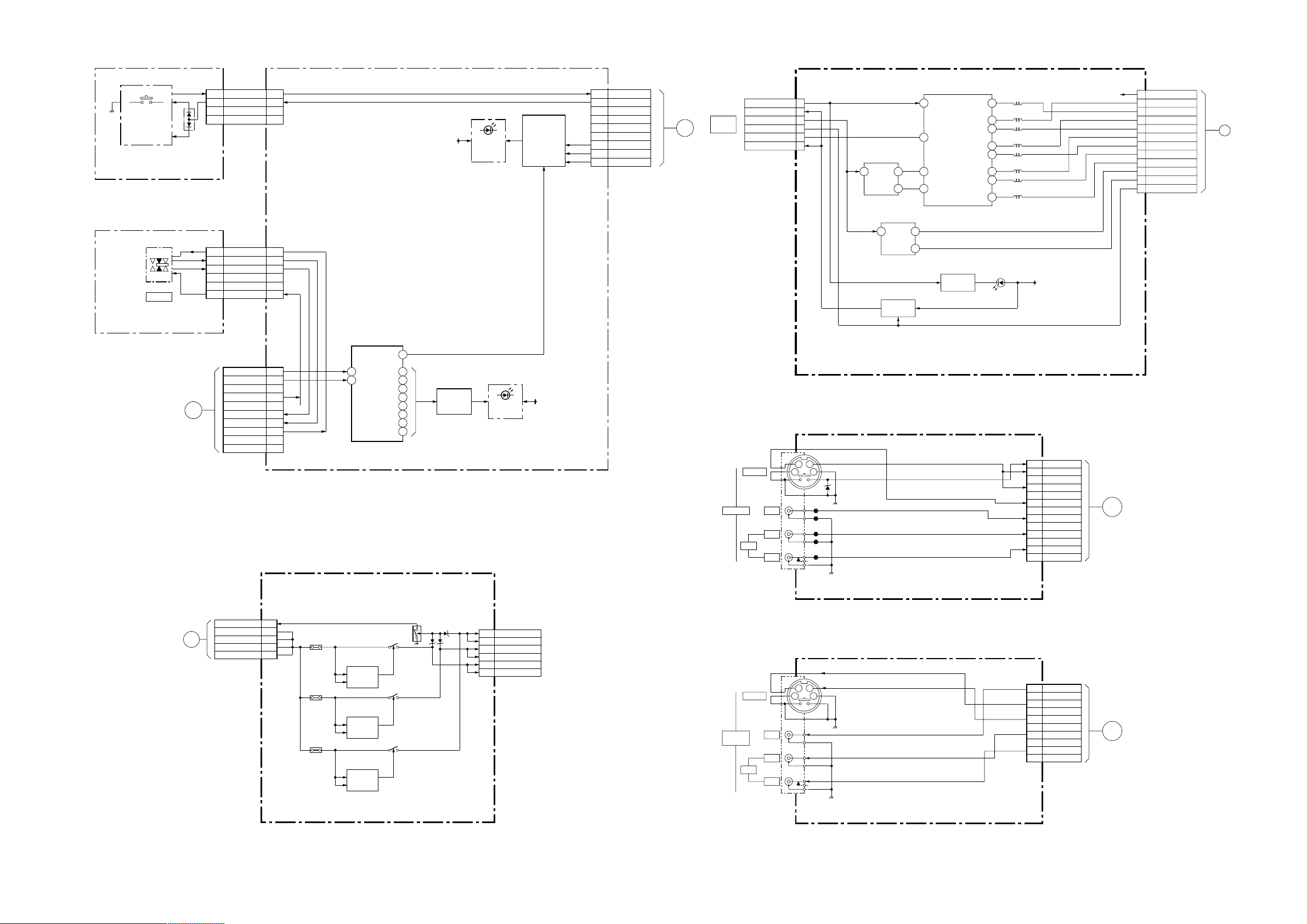
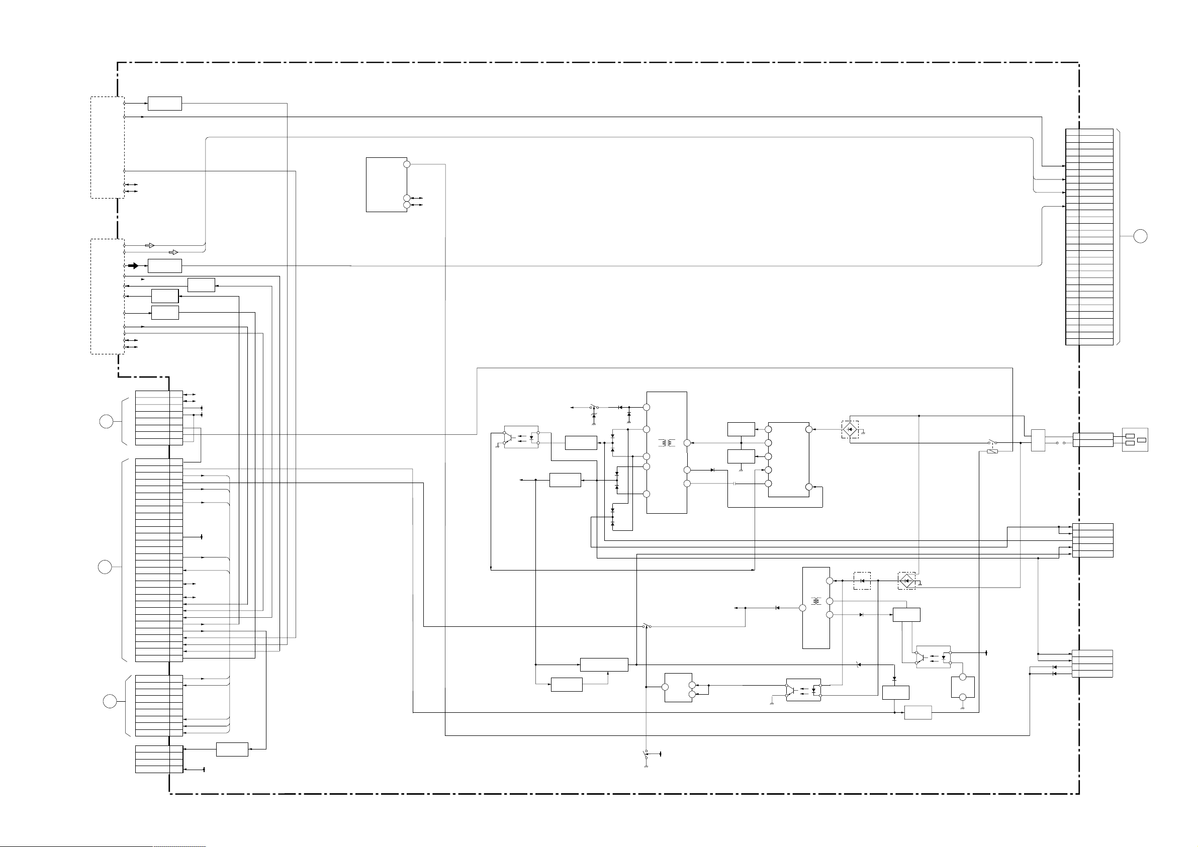
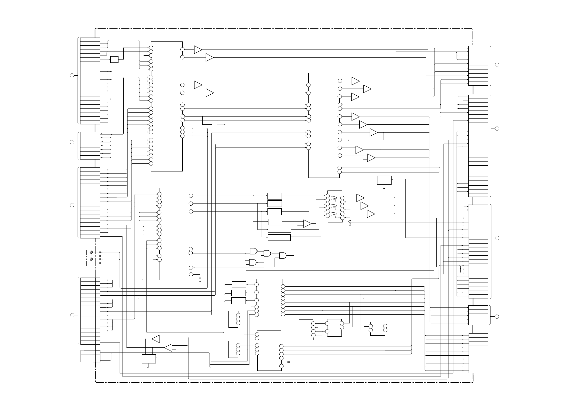
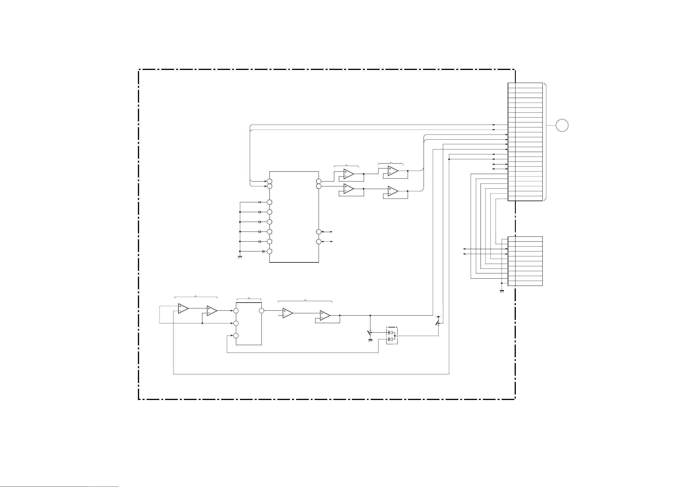
4-1-2. MEDIA RECEIVER UNIT (MBT-MR1)
IC1402
IC1403
IC1401
CN8005
(MEMORY STICK)
TO IFA BOARD
L404
L403
L402
L401
+3.3V
D1409
STIK
MEMORY
CN1401
3.3V
VCC SW
Q1403
Q1401,1402
LED DRIVE
LVDS DRV
DI1 DI- 7
82DI+
DO
2
DO
DE
CK
4113
5
11
3
DEA
BUS SW
15
14
10
7
9
6
2
MS2
VCC
MS-INS
VCC
MS SDO+
MS SCLK-
MS SCLK+
MS SDIR-
MS INS
MS SDIR+
MS SDI-
MS BS-
MS SDI+
MS BS+
LVDS RECEIVER
BS
DO+
DO-
CK-
CK+
DIR-
DIR+
BS+
BS- 1
CN1402
5
3
7
6
9
8
12
11
14
13
10
15
3.3VD
MS SDO-
3
4
2
6
8
9
MS-SDIO
MS-BS
MS-SCLK
I
CN171
4
D171
3
2
1
S171-176
H3(KEY)
CN191
1
2
3
4
S191
POWER
5
6
H4(POWER SW)
A
TO A BOARD
CN6203
KEY1
KEY-WAKE
GND
GND
P-SW(+)
P-SW(-)
P-ON
E
E
STBY+5V
CN105
SCL
SDA
SDT5V
STBY5V
GND
P-ON
P-SW(-)
P-SW(+)
GND
GND
CN107
1
2
3
4
CN106
6
5
4
3
2
1
1
2
3
4
5
6
7
8
9
10
IC101
LED DRIVE
20
SCL A03
SDA
21
A02 2
A04
DA5
DA6
DA7
DA8
DA9
DA10 10
CN101
1
KEY1
2
KEY_WAKE
GND
3
4
NC
5
NC
6
5V TO ABOARD
D126,D127
3
4
5
6
7
8
9
Q101-108
LED DRIVE
D101-108
Q117-124
LED SW
5V
7
8
9
TIMER LED
NC
P_LED
STBY_LED
H1(LED)
B
CN6204
S VIDEO
VIDEO IN2 VIDEO
L
AUDIO
R
J40
43
21
CN43
1
2
3
4
5
6
7
8
9
10
11
12
13
V2
V2
V2
V2
V2
V2
V2
-SW
-S2
GND
-C
GND
-Y
GND
-V
GND
-L
GND
-R
GND
F
TO AD BOARD
CN4001
H2
(VIDEO2 INPUT, VOLUME CONTROL)
CN1604
1
17
18
19
20
PS1603
IC1605
1.8V DC-DC CONV.
1
VIN
VOUT
5
CONT
PS1602
IC1604
3.3V DC-DC CONV.
1
VOUT
VIN
5
CONT
PS1601
IC1603
2.5V DC-DC CONV.
1
VOUT
VIN
5
CONT
(DC-DC CONVERTER)
DP
OVP
D6.5V
TO IFA
BOARD
CN8011
N
D6.5V
D6.5V
D6.5V
4
4
4
Q1614
Q1611
Q1613
Q1610
Q1612
Q1609
Q1608
D1605D1606
D1604
2
3
5
6
8
9
CN1601
2.5V
2.5V
3.3V
3.3V
1.8V
1.8V
TO DICA
BOARD
CN402
MONITOR
OUT
AUDIO
S VIDEO
VIDEO
L
R
J9405
CN9406
M-V
43
21
1
D
GND
2
M-Y
3
4
GND
5
M-C
6
GND
7
M-L
8
GND
9
M-R
10
GND
E
TO AD BOARD
CN4301
U2
(MONITOR OUT)
KE-61MR1 (K) 4-6
TU6201(S)
DET OUT 2
DE-EM OUT
AFT OUT
SCL
SDA
TU6202(M)
L OUT
R OUT
DET OUT 2
F MONO
MODE
RF AGC
DET OUT
AFT OUT
SAP IND
SCL
SDA
SCL
SDA
AUDIO L
VIDEO
SCL
SDA
BUFFER
Q6201
,Q6202
AUDIO R
BUFFER
,
Q6205
INVERTER
Q6203
BUFFER
Q6201
SW
Q6206
IC6200
SW CONTROL
FSW
CLK
DAT
CN6211
GND
1
STU-R
2
GND
3
STU-L
4
G
2
SCL
15
14
SDA
5
6
7
8
9
10
11
12
13
14
SCL(I2C-1)
15
SDA(I2C-1)
16
17
18
19
20
21
22
23
24
25
26
27
28
29
30
31
32
STU-V
G
MTU-R
G
MTU-L
G
NTU-V
G
G
G
SET5V
SET5V
SET5V
SET5V
SET5V
SET5V
STBY 5V
G
SET9V
SET9V
SET9V
SET9V
SET9V
SET9V
SET9V
D
TO AD BOARD
CN4002
A
TO H1 BOARD
CN105
C
TO M BOARD
CN5210
B
TO H1 BOARD
CN101
TO ANT SW
CN6203
SCL
1
SDA
2
SET5V
3
STBY5V
P-SW(-)
P-SW(+)
AC RLY
TIMER LED
AC DET
P-INT2
P-LED
BS REC
LB ERR
SET 5V
KEY-WAKE
MAIN AFT
I SAP
O SAP
SUB AFT
SUB HSYNC
FMONO
KEY-WAKE
P-LED
STBY LED
TIMER LED
4
5
G
6
P-ON
7
8
CN6201
PON
1
2
3
4
5STBY LED
6
7
8
9
NC
10
11NC
12
13
NC
14G
15
16
G
17
KEY1
18
G
19
SDA SDA
20G
SCL SCL
21
22
23
24
25
AGC
26ANT SW
27
28
29
30MAIN HSYNC
CN6204
KE1
1
2
3
G
4
NC
5
NC
NC
6
7
8
9
CN6205
MS
1
2
G
3
NC
4
9V
SCL
SDA
SET5V
STBY5V
SET 5V
+9V
ANT SE
Q6207
PH6002
MAIN CONTROL
BS9V
T6002
Q6014
TU33V
CONTROL
3
IC6005
CONTROL
IC007
12
Q6001,6002
SW
D6032
D6024
D6020
D6023
IC6001
3.3VREG
D6021
5
13
D6019
8
11
6
7
Q6006
AC OFF SW
Q6009,6011
IC6008
9
Q2
STBY 5V
IC6002
CONVERTER
Q6004
2
CONVERTER
Q6003
D6519
4
1
STBY 5V
5
A2
11
B2
DRIVER
16
VG
15
VS
12
VG
2
F/B
9
OCP
D6018
1
H
VSENCE
)()(L
8
VC1
10
PH6001
MAIN CONTROL
T6003
D6004
RY6001
D6009,
D6010,
D6007
D6012,
1
3
5
D6013
5
4
IC6003
D6016
D6003
A
CONVERTER
1
2
PH6003
MAIN CONTROL
STBY 5V
D6031
Q6010
RY DRIVE
Q6010
RY DRIVE
3
IC6004
V REF
2
(POWER, FAN CONTROL)
T6001
FILTER
D6101
~
F6001
D6102
CN6001
AC(L)2
1
AC(N)
CN6004
D6.5V
1
2 D6.5V
SET6.5V
4
SET11V
6
8 LVDS3.3V
CN6101
FAN POW
1
FAN POW
2
3
FAN PROT 1
FAN PROT 2
4
AC INLET
G
TO
IFA BOARD
CN8008
TO FAN
KE-61MR1 (K) 4-7
D
TO A BOARD
CN6211
F
TO H2 BOARD
CN43
G
TO U1 BOARD
CN9401
J7001
H
TO U1 BOARD
CN9402
CN4002
STU-R
STU-L
STU-V
MTU-R
MTU-L
MTU-V
SCL(I2C-1)
SDA(I2C-1)
BS5V
BS5V
SET5V
SET5V
SET5V
SET5V
STBY5V
BS9V
BS9V
BS9V
BS9V
SET9V
SET9V
SET9V
CN4001
V2-SW
V2-S2
V2-C
V2-Y
V2-V
V2-L
V2-R
CN4003
V1-SW
V1-S2
V1-V
V1-Y
V1-C
V1-L
V1-R
V3-SW
V3-S2
V3-V
V3-Y
V3-C
V3-L
V3-R
LINE-L
LINE-R
STBY5V
CS-OUT
CN4501
D1-Y
D1-CB
D1-CR
D1-L
D1-R
D2-Y
D2-CB
D2-CR
D2-L
D2-R
D2-L1
D2-L2
D2-L3
D2-SW
S-WOOFER
CN7004
UB_BINT
SDA
SCL
AD
IC4001
SCL
SDA
63
62
64
60
59
61
1
3
5
2
4
6
7
15
17
19
16
18
20
21
22
24
26
23
25
27
28
7
V-IN2
Y-IN2
AV SW1
RFMAIN_V
RFMAIN_L
RFMAIN_R
RFSUB_V
RFSUB_V
RFSUB_V
C-IN2
L-IN2
R-IN2
S2-IN2
SW-IN2
V-IN2
Y-IN2
C-IN2
L-IN2
R-IN2
S2-IN2
SW-IN2
V-IN3
Y-IN3
C-IN3
L-IN3
R-IN3
S2-IN3
SW-IN3
44
IN2-H/L1
45
IN2-V/L1
46
IN2-L3
47
IN2-SW
41
IN2-1
42
IN2-2
43
IN2-3
1
IN3-1
2
IN3-2
3
IN3-3
7
IN4-1
8
IN4-2
9
IN4-3
30
SCL
31
SDA
5
+
6
+
1
56
SUB Y
58
SUB C
44
MAIN Y/V
47
MAIN C
52
SUB L
54
SUB R
33
SCL
34
SDA
30
AVM-V
29
AVM-L
31
AVM-R
IC4501
COMPONENT-I/F
SUB Y
SUB C
SUB C
SELVOUT
SELHOUT
CLAMP SW
EXTCLK/XTAL
IC4301 AMP
3
+
2
-
Q4012,4006
FL4151
Q4011,4005
FL4150
Q4014
56
58
58
23
22
17
20
X4501
Q4013
SDA
SCL
FL7004
FL7003
FL7002
IC7001
NVM
SCK
SI
WP
IC7006
NVM
SCK
SI
WP
IC4303
AV SW2
17
19
2
MAIN_L
4
MAIN_R
62
SUB L
BS/VIDEO VOUT
64
SUB R
23
D2 L
25
D2 R
16
D1 L
18
BS/VIDEO L
D1 R
BS/VIDEO R
SEL_L OUT
SEL_R OUT
Q4509,4512
BUFFER
Q4507,4511
BUFFER
Q4508,4510
BUFFER
Q4503,4506
BUFFER
Q4502,4505,FL4502
LPF
Q4501,1504,FL4501
LPF
IC4504
2
3
12
11
6
5
7
6
5
7
NOR
1
5
6
13
16
IOB/PR
13
IOG/PB
10
IOR/Y
33
RESETN
32
SDA
31
SCL
11
PA2/SCL
19
PA2/SDA
24
PA2/SCL
29
PA2/SDA
10
AINT/IT8/PB7
IC7004
IC7005
OSCOUT
4
RX2+
RX2RX1+
RX1-
RX0+
RX0-
RXC+
RXC-
RESET
MUTE
VGA
OSCIN
9
8
46
47
52
53
58
59
61
62
8
21
18
2
3
10
X7002
12MHz
IC4503 BUFFER
5
+
7
6
-
IC7009
1
6
2
5
31
29
27
25
23
21
18
17
15
14
13
12
11
10
9
7
6
5
4
3
2
1
1
2
4
6
8
10
12
30
29
28
26
24
22
20
18
17
16
14
12
10
8
6
5
3
2
28
26
24
22
20
18
16
14
12
10
8
7
6
5
1
3
1
2
Q4018
BUFFER
BS5V
SET5V
BS9V
STBY5V
Q4305,4301
Q4321
MUTE
(AV SW,COMPONENT-I/F,DVI)
3
2
5
6
Q4519
SW
Q4310
Q4308
Q4309
IC4306 BUFFER
7
8
4
IC4307 BUFFER
7-+
3
+
2
-
Q516
BUFFER
Q4515
Q4514
IC7007
1
2
6
1
Q4312,4315
4316,4401
MUTE
BUFFER
BUFFER
6
5
ATW-YV
MAIN Y/V
SUB Y
Y IN
C IN
Y OUT
COUT3
DCOUT
IC4502
VIDEO SW
9
8
14
11
1
16
IC7008
1
2
53
44
47
3
5
41
39
37
36
38
40
43
45
6
7
5
12
3
2
5
6
SET9V
SCL
SDA
SDA
SCL
CN4004
ATW-YV
1
COMP IN CR
3
COMP IN CB
5
COMP IN V
7
MAIN IN Y/V
9
SUB IN Y/V
11
MAIN IN C
13
SUB IN C
15
COMB OUT Y
17
COMB OUT C
19
CN4306
1
SET9V
2
SET9V
4
CLK
5
DAT
7
SUR-L
9
SUR-R
11
WF OUT
17
MAIN L
19
MAIN R
21
VAL L
23
VAL R
25
WOOFER MUTE
39
BINT
41
ROM-SCL
42
ROM-SDA
44
ROM-WP
46
BUS-SEL
48
TMDS-RST
CN4005
2
SDA(STBY)
3
SCL(STBY)
6
SYNC SW
7
NT SW
8
CLAMP GATE
10
LINE MUTE
11
SBWR MUTE
12
REC_OUT MUTE
15
CNTRL-S
19
MAIN L
21
MAIN R
23
VAR L
25
VAR R
27
DVI-RST1VGA
28
VGA
29
MUTE
31
BINT
33
ROM-SCL
34
ROM-SDA
35
ROM-WP
36
BUS-SEL
37
TMDS-RST
CN4301
M-V
10
M-Y
8
M-C
6
M-L
4
M-R
2
CN7001
RX2-
1
RX2+
2
SCL
6
SDA
7
RX1-
9
RX1+
10
RX0-
17
RX0+
18
RXC-
23
RXC+
24
K
TO IFA BOARD
CN8003
J
TO AU BOARD
CN4703
L
TO M BOARD
CN5230
E
TO U2 BOARD
CN9406
KE-61MR1 (K) 4-8
CN4703
5.1 OUT FL
27
5.1 OUT FR
29
5.1 OUT RL
31
33
5.1 OUT RR
5.1 OUT C--
35
5.1 OUT LFE
--
37
5.1 CHDM-L-
13
5.1 CHDM-R-
15
SUR-L
7
SUR-R
9
17
MAIN L
MAIN R
19
11
WF OUT
WOOFER MUTE
25
VER L
IC4704
SDA
SCL
7
BUFFER
3
2
5
6
Q4707,4710
MUTE
1
7
IC4703
SURROUND
64
L IN
63
R IN
62
FL IN
61
FR IN
60
RL IN
59
PR IN
58
C IN
57
SW IN
IC4705
MIX/LPF
3
2
5
1
7
6
7
6
5
IC4708
CH0
CH1
SEL
COM
IC4706
2
1
1
3
OUTA
OUTB
SDA
SCA
16
36
22
23
5
6
IC4707
BUFF
3
2
5
6
1
7
Q4708,4709
MUTE
SCL
SDA
SDA
SCL
9V
21
VER R
23
CLK
4
DAT
5
TMDS-RST
48
BUS-SEL
46
ROM-WP
44
ROM-SCL
41
42
ROM-SDA
39
BINT
1
GND
2
BINT
3
SDA
4
SCL
5
ROM-SDA
ROM-SCL
6
7
ROM-WP
8
BUS-SEL
TMDS-RST
9
GND
10
CN4704
J
TO AD BOARD
CN4306
AU(SURROUND)
D4707
KE-61MR1 (K) 4-9
 Loading...