

Sony KDL-70XBR3 Schematic

HISTORY INFORMATION FOR THE FOLLOWING MANUAL:
SERVICE MANUAL
MODEL NAME REMOTE COMMANDER DESTINATION
KDL-70XBR3
RM-YD013 US
FIXP
CHASSIS
ORIGINAL MANUAL ISSUE DATE: 2/2007
REVISION DATE SUBJECT
2/2007 No revisions or updates are applicable at this time.
4/2007 Reissue entire manual to include Disassembly insturctions.
:UPDATED ITEM
☛
LCD DIGITAL COLOR TELEVISION
9-883-735-02

Self Diagnosis
Supported model
SERVICE MANUAL
MODEL NAME REMOTE COMMANDER DESTINATION
KDL-70XBR3
RM-YD013 US
FIXP
CHASSIS
9-883-735-02
KDL-70XBR3
LCD DIGITAL COLOR TELEVISION

KDL-70XBR3
TABLE OF CONTENTS
SECTION TITLE PAGE SECTION TITLE PAGE
Specifi cations ................................................................................. 4
Warnings and Cautions .................................................................. 6
Safety-Related Component Warning .............................................. 7
Safety Check-Out ........................................................................... 9
Self-Diagnostic Function ............................................................... 10
SECTION 1: DISASSEMBLY ............................................................... 12
1-1. Overview .............................................................................. 12
1-2. LVDS Cable Removal .......................................................... 12
1-3. Rear cover removal .............................................................. 13
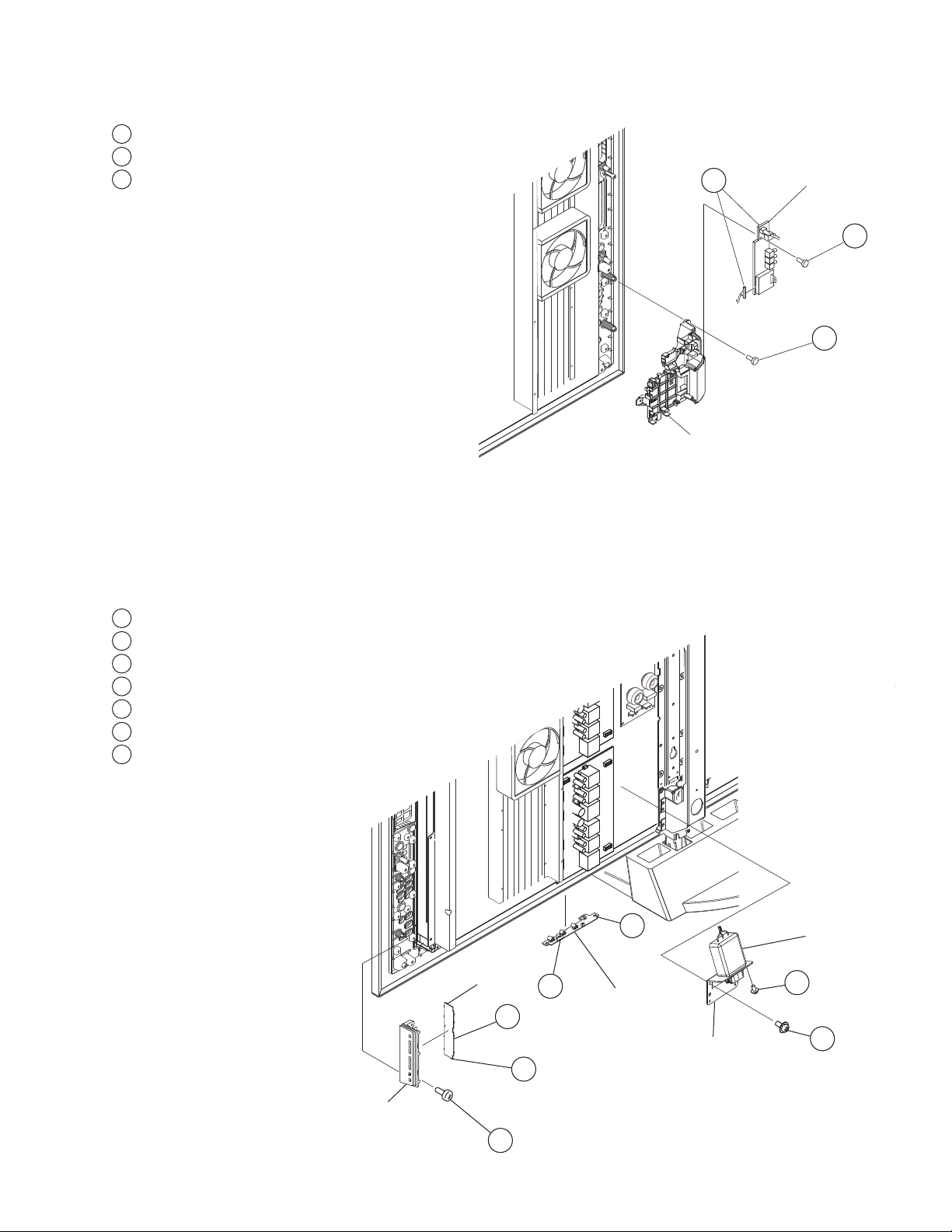
1-4. Fan Removal ........................................................................ 13
1-5. H5 Board and Side Terminal Bracket Removal .................... 14
1-6. H1 board, H3 board, and AC Inlet Removal ......................... 14
1-7. Speaker Removal ................................................................. 15
1-8. G1P board removal .............................................................. 15
1-9. AU board and QT Board Removal ....................................... 16
1-10. BEP board and QM Board Removal .................................... 16
1-11. G2P Board and F Board Removal ....................................... 17
1-12. LT3 Board, LP3 Boards, and LD3 Board
(LED Backlight Drivers) Removal ......................................... 17
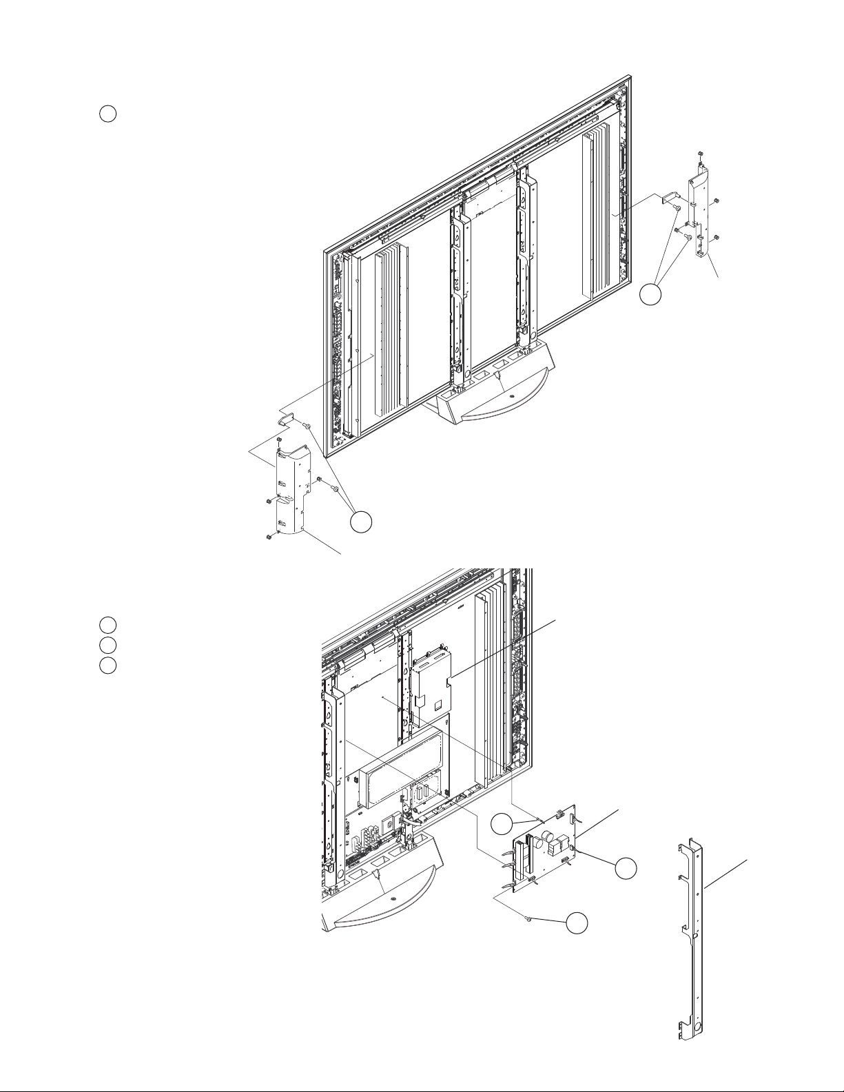
1-13. Front Cabinet, Base Stand, and Arm Bracket Removal ....... 18
SECTION 2: SERVICE ADJUSTMENTS ............................................. 19
2-1. Overview .............................................................................. 19
SECTION 3: DIAGRAMS ..................................................................... 20
3-1. Circuit Boards Location ........................................................ 20
3-2. Printed Wiring Boards and
Schematic Diagrams Information ......................................... 21
3-3. Block Diagrams .................................................................... 23
System Block Diagram ......................................................... 23
Connections Diagram ........................................................... 24
3-4. Schematics and Supporting Information .............................. 25
AUP Board Schematic Diagram (1 of 7) .............................. 25
AUP Board Schematic Diagram (2 of 7) .............................. 26
AUP Board Schematic Diagram (3 of 7) .............................. 27
AUP Board Schematic Diagram (4 of 7) .............................. 28
AUP Board Schematic Diagram (5 of 7) .............................. 29
AUP Board Schematic Diagram (6 of 7) .............................. 30
AUP Board Schematic Diagram (7 of 7) .............................. 31
BEP Board Schematic Diagram (1 of 13) ............................. 34
BEP Board Schematic Diagram (2 of 13) ............................. 35
BEP Board Schematic Diagram (3 of 13) ............................. 36
BEP Board Schematic Diagram (4 of 13) ............................. 37
BEP Board Schematic Diagram (5 of 13) ............................. 38
BEP Board Schematic Diagram (6 of 13) ............................. 39
BEP Board Schematic Diagram (7 of 13) ............................. 40
BEP Board Schematic Diagram (8 of 13) ............................. 41
BEP Board Schematic Diagram (9 of 13) ............................. 42
BEP Board Schematic Diagram (10 of 13) ........................... 43
BEP Board Schematic Diagram (11 of 13) ........................... 44
BEP Board Schematic Diagram (12 of 13) ........................... 45
BEP Board Schematic Diagram (13 of 13) ........................... 46
F Board Schematic Diagram ................................................ 49
G1P Board Schematic Diagram (1 of 2) ............................... 50
G1P Board Schematic Diagram (2 of 2) ............................... 51
G2P Board Schematic Diagram ........................................... 54
H1 Board Schematic Diagram .............................................. 57
H3 Board Schematic Diagram .............................................. 58
H4 Board Schematic Diagram .............................................. 60
H5 Board Schematic Diagram (1 of 2) ................................. 61
H5 Board Schematic Diagram (2 of 2) ................................. 62
QM Board Schematic Diagram (1 of 5) ................................ 65
QM Board Schematic Diagram (2 of 5) ................................ 66
QM Board Schematic Diagram (3 of 5) ................................ 67
QM Board Schematic Diagram (4 of 5) ................................ 68
QM Board Schematic Diagram (5 of 5) ................................ 69
QT Board Schematic Diagram ............................................. 72
3-5. Semiconductors ................................................................... 75
SECTION 4: EXPLODED VIEWS ........................................................ 76
4-1. Rear Cover Assembly ......................................................... 76
4-2. H Boards and Speakers ....................................................... 77
4-3. Chassis ................................................................................ 78
4-4 Connectors ........................................................................... 79
4-5. Cabinet and Stand Assemblies, and H4 Board .................... 80
SECTION 5: ELECTRICAL PARTS LIST ............................................ 81
APPENDIX A: ENCRYPTION KEY COMPONENTS ..........................A-1
KDL-70XBR3
3
SPECIFICATIONS
y
KDL-70XBR3
Power Requirements
Power Consumption (W)
In Use (Max)
In Standby
120V AC, 60Hz
650W
Less than 0.5W
VIDEO (IN) 1/2/4:
S Video (4-Pin Mini DIN (VIDEO 1 Only)
Y: 1.0 Vp-p, 75 ohms unbalanced, sync negative
C: 0.286 Vp-p (Burst signal), 75 ohms
Video
1.0 Vp-p, 75ohms unbalanced, sync negative
Audio
500 mVrms (100% modulation)
Impedance:47 kilohms
HD/DVD IN 5/6:
YP
(Component Video)
BPR
Y:1.0 Vp-p, 75 ohms unbalanced, sync negative
PB:0.7 Vp-p, 75 ohms
PR:0.7 Vp-p, 75 ohms
Signal format: 480i, 480p, 720p, 1080i
AUDIO
500 mVrms (100% modulation)
Impedance: 47 kilohms
HDMI IN 3/7/8:
HDMI: Video:480i, 480p, 720p, 1080i,
1080p (except for HDMI IN 3)
Audio: Two channel linear PCM 32, 44.1 and
48 kHz, 16, 20 and 24 bits
AUDIO (for HDMI IN 8):
500 mVrms (100% modulation) (Fixed)
Impedance: 47 kilohms
AUDIO OUT:
500 mVrms (100% modulation) (Fixed)
1 Vrms at the maximum volume setting (Variable)
DIGITAL OUT (OPTICAL):
Optical Digital Audio Output (PCM/Dolby digital)
PC IN 9:
D-sub 15-pin, analog RGB, 0.7 Vp-p, 75 ohms, positive
See the PC Input Signal Reference in Operating Instructions.
PC AUDIO INPUT:
Stereo mini jack, 500 mVrms (100% modulation),
Impedance: 47 kilohms
HEADPHONES:
Stereo mini jack
Impedance: 16 ohms
Trademark Information
TruSurround XT, SRS and ( ) symbol are trademarks of SRS Labs, Inc.
TruSurround XT technology is incorporated under license from SRS Labs,
Inc.
Manufactured under license from BBE Sound, Inc.
Licensed by BBE Sound, Inc. under one or more of the following US
patents: 5510752, 5736897. BBE and BBE symbol are registered
trademarks of BBE Sound, Inc.
Macintosh is a trademark licensed to Apple Computer, Inc., registered in
the U.S.A and other countries.
Blu-ray Disc is a trademark.
“BRAVIA” and are trademarks of Sony Corporation.
“x.v.Color” is a trademark of Sony Corporation.
HDMI, the HDMI logo and High-Definition Multimedia Interface are
trademarks or registered trademarks of HDMI Licensing, LLC.
KDL-70XBR3
As an ENERGY STAR
determined that this product meets the ENERGY STAR
guidelines for energy efficiency.
ENERGY STAR
This TV incorporates High-Definition
Multimedia Interface (HDMI™) technology.
Manufactured under license from Dolby
Laboratories. “Dolby” and the double-D symbol are
trademarks of Dolb
®
Partner, Sony Corporation has
®
is a U.S. registered mark.
Laboratories.
®
Design and specifi cations are subject to change without notice.
4
Dimensions (W x H x D)
with stand
Dimensions (W x H x D)
without stand
Mass
with stand 205 lbs.
without stand 176 lbs.
Speakers
Output
Dimensions (W x H)
Tweeter
Dimensions (H)
KDL-70XBR3
5/8
5/8
72
x 44
x 16
5/8
inches
1842 x 1131 x 422 mm
5/8
x 42
1/4
x 6 inches
72
1842 x 1073 x 150 mm
93.0 kg
80.0 kg
11W x 11W
4 x (2 x 4
1/4
inches)
4 x (50 x 105 mm)
5/8
2 x (1
inches)
2 x (40 mm)
KDL-70XBR3
Television system
American TV Standard
ATSC (8VSB terrestrial) ATSC compliant 8VSB
QAM on cable ANSI/SCTE 07 2000
Channel coverage
Analog
2-69 Terrestrial
1-125 Cable
Digital
2-69 Terrestrial
1-135 Cable
Antenna
75-ohm external terminal for VHF/UHF
Panel System
LCD (Liquid Crystal Display) Panel
Display Resolution (horizontal x vertical):
1,920 dots x 1,080 lines
Screen Size (measured diagonally)
KDL-70XBR3 - 70 inches
Supplied Accessories
Remote Commander RM-YD013
Two Size AA (R6) Batteries
75-ohm coaxial cable
AC Power Cord
AC Plug Holder
HD15-HD15 Cable
Support Belt, Securing Screw, and Wood Screw
Guide sticker (Lx2, Rx2)
Operating Instructions
Quick Setup Guide
Installing the Wall-Mount Bracket
Warranty Card
Optional Accessories
Headphones Plug Adaptor
Connecting Cables
Wall-Mount Bracket: SU-WL500
KDL-70XBR3
5

KDL-70XBR3
WARNINGS AND CAUTIONS
CAUTION
These servicing instructions are for use by qualifi ed service personnel only. To reduce the risk of electric shock, do not perform any
servicing other than that contained in the operating instructions unless you are qualifi ed to do so.
WARNING!!
An isolation transformer should be used during any service to avoid possible shock hazard, because of live chassis. The chassis of
this receiver is directly connected to the ac power line.
! SAFETY-RELATED COMPONENT WARNING!!
Components identifi ed by shading and ! mark on the schematic diagrams, exploded views, and in the parts list are critical for safe
operation. Replace these components with Sony parts whose part numbers appear as shown in this manual or in supplements
published by Sony. Circuit adjustments that are critical for safe operation are identifi ed in this manual. Follow these procedures
whenever critical components are replaced or improper operation is suspected.
ATTENTION!!
Ces instructions de service sont à l’usage du personnel de service qualifi é seulement. Pour prévenir le risque de choc électrique, ne
pas faire l’entretien autre que celui contenu dans le Mode d’emploi à moins que vous soyez qualifi é faire ainsi.
Afi n d’eviter tout risque d’electrocution provenant d’un chássis sous tension, un transformateur d’isolement doit etre utilisé lors de tout
dépannage. Le chássis de ce récepteur est directement raccordé à l’alimentation du secteur.
! ATTENTION AUX COMPOSANTS RELATIFS A LA SECURITE!!
Les composants identifi es par une trame et par une marque ! sur les schemas de principe, les vues explosees et les listes de pieces
sont d’une importance critique pour la securite du fonctionnement. Ne les remplacer que par des composants Sony dont le numero
de piece est indique dans le present manuel ou dans des supplements publies par Sony. Les reglages de circuit dont l’importance
est critique pour la securite du fonctionnement sont identifi es dans le present manuel. Suivre ces procedures lors de chaque
remplacement de composants critiques, ou lorsqu’un mauvais fonctionnement suspecte.
CARRYING THE TV
Carrying the TV in the specified manner
To avoid dropping the TV and causing serious injury, be sure to follow
these guidelines:
s Before carrying the TV set, disconnect all cables.
s Carrying this TV set requires at least four people.
s When you carry the TV set, place your hand as illustrated and hold it
securely. Do not put stress on the LCD panel and the frame around the
screen.
s When lifting or moving the TV set, hold it firmly from the bottom.
Two people who carry the center position of the TV at the rear side,
hold the handles at the rear of the TV.
s When carrying the TV set, do not subject it to shocks or vibration, or
excessive force.
KDL-70XBR3
6
SAFETY-RELATED COMPONENT WARNING
KDL-70XBR3
There are critical components used in LCD color TVs that are important for safety. These components are identifi ed with shading and
mark on the schematic diagrams and the electrical parts list. It is essential that these critical parts be replaced only with the part number
specifi ed in the electrical parts list to prevent electric shock, fi re, or other hazard.
NOTE: Do not modify the original design without obtaining written permission from the manufacturer or you will void the original parts and
labor guarantee.
!
USE CAUTION WHEN HANDLING THE LCD PANEL
When repairing the LCD panel, be sure you are grounded by using a wrist band.
When installing the LCD panel on a wall, the LCD panel must be secured using the 4 mounting holes on the rear cover.
To avoid damaging the LCD panel:
do not press on the panel or frame edge to avoid the risk of electric shock.
do not scratch or press on the panel with any sharp objects.
do not leave the module in high temperatures or in areas of high humidity for an extended period of time.
do not expose the LCD panel to direct sunlight.
avoid contact with water. It may cause a short circuit within the module.
disconnect the AC adapter when replacing the backlight (CCFL) or inverter circuit.
(High voltage occurs at the inverter circuit at 650Vrms.)
always clean the LCD panel with a soft cloth material.
use care when handling the wires or connectors of the inverter circuit. Damaging the wires may cause a short.
protect the panel from ESD to avoid damaging the electronic circuit (C-MOS).
LEAKAGE CURRENT HOT CHECK CIRCUIT
KDL-70XBR3
7
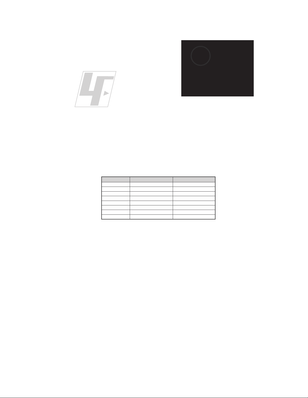
The circuit boards used in these models have been processed using
Lead Free Solder. The boards are identified by the LF logo located
close to the board designation e.g. H1 etc [ see example ]. The
servicing of these boards requires special precautions to be taken as
outlined below.
KDL-70XBR3
example 1
It is strongly recommended to use Lead Free Solder material in order to guarantee optimal quality of new solder joints.
Lead Free Solder is available under the following part numbers :
rebmuntraP retemaiD skrameR
91-500-046-7mm3.0gK52.0
02-500-046-7mm4.0gK05.0
12-500-046-7mm5.0gK05.0
22-500-046-7mm6.0gK52.0
32-500-046-7mm8.0gK00.1
42-500-046-7mm0.1gK00.1
52-500-046-7mm2.1gK00.1
62-500-046-7mm6.1gK00.1
Due to the higher melting point of Lead Free Solder the soldering iron tip temperature needs to be set to 370 degrees centigrade.
This requires soldering equipment capable of accurate temperature control coupled with a good heat recovery characteristics.
For more information on the use of Lead Free Solder, please refer to
http://www .sony-training.com
KDL-70XBR3
8
SAFETY CHECK-OUT
KDL-70XBR3
After correcting the original service problem, perform the following
safety checks before releasing the set to the customer:
1. Check the area of your repair for unsoldered or poorly soldered
connections. Check the entire board surface for solder splashes and
bridges.
2. Check the interboard wiring to ensure that no wires are “pinched” or
touching high-wattage resistors.
3. Check that all control knobs, shields, covers, ground straps, and
mounting hardware have been replaced. Be absolutely certain that
you have replaced all the insulators.
4. Look for unauthorized replacement parts, particularly transistors,
that were installed during a previous repair. Point them out to the
customer and recommend their replacement.
5. Look for parts which, though functioning, show obvious signs of
deterioration. Point them out to the customer and recommend their
replacement.
6. Check the line cords for cracks and abrasion. Recommend the
replacement of any such line cord to the customer.
7. Check the antenna terminals, metal trim, “metallized” knobs, screws,
and all other exposed metal parts for AC leakage. Check leakage as
described below.
The AC leakage from any exposed metal part to earth ground and
from all exposed metal parts to any exposed metal part having a
return to chassis, must not exceed 0.5 mA (500 microamperes).
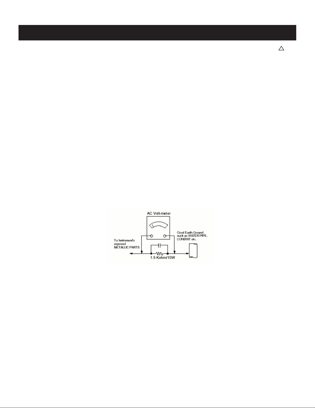
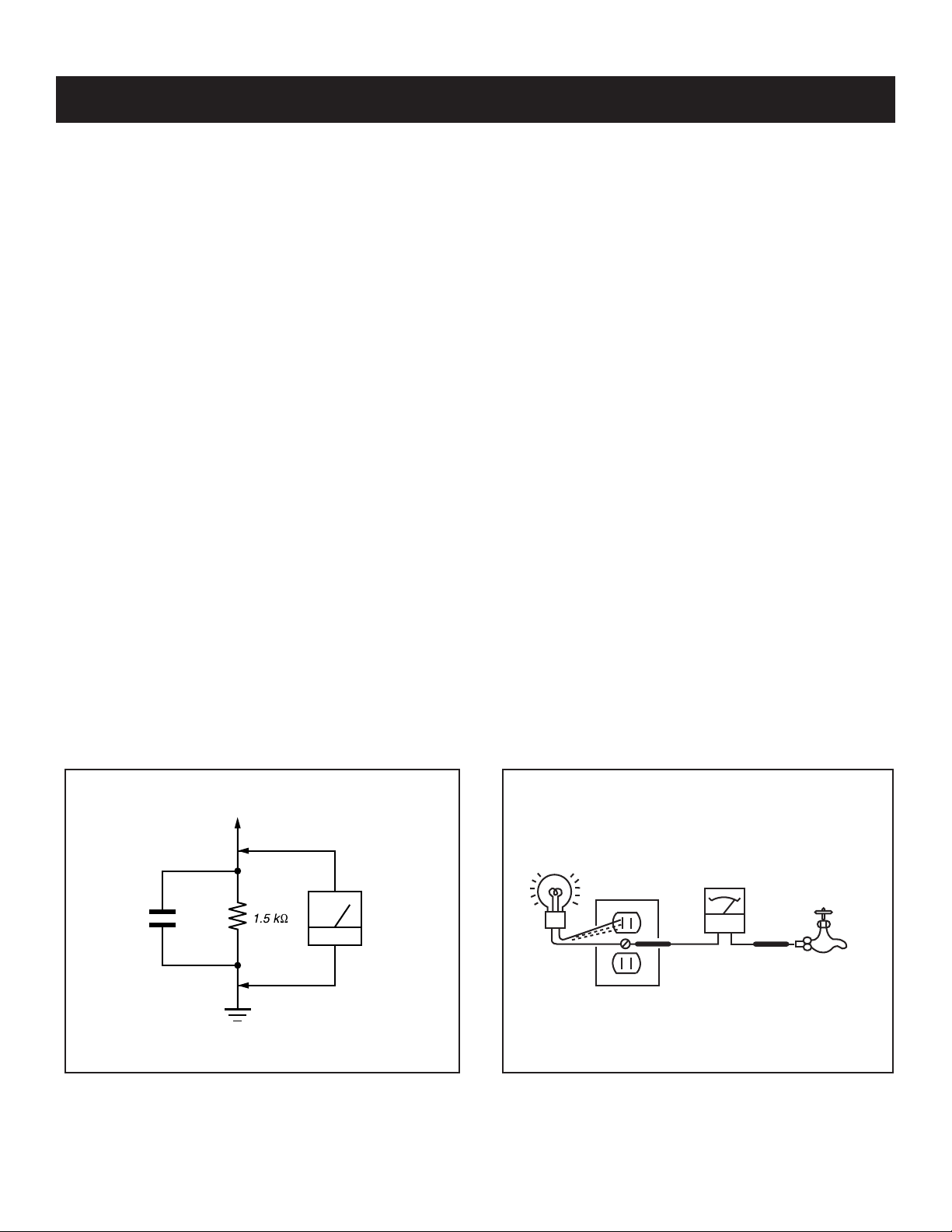
Leakage current can be measured by any one of three methods.
1. A commercial leakage tester, such as the Simpson 229 or RCA
WT-540A. Follow the manufacturers’ instructions to use these
instructions.
2. A battery-operated AC milliampmeter. The Data Precision 245
digital multimeter is suitable for this job.
3. Measuring the voltage drop across a resistor by means of a VOM
or battery-operated AC voltmeter. The “limit” indication is 0.75
V, so analog meters must have an accurate low voltage scale.
The Simpson’s 250 and Sanwa SH-63TRD are examples of
passive VOMs that are suitable. Nearly all battery-operated digital
multimeters that have a 2 VAC range are suitable (see Figure A).
How to Find a Good Earth Ground
A cold-water pipe is a guaranteed earth ground; the cover-plate
retaining screw on most AC outlet boxes is also at earth ground. If the
retaining screw is to be used as your earth ground, verify that it is at
ground by measuring the resistance between it and a cold-water pipe
with an ohmmeter. The reading should be zero ohms.
If a cold-water pipe is not accessible, connect a 60- to 100-watt
trouble- light (not a neon lamp) between the hot side of the receptacle
and the retaining screw. Try both slots, if necessary, to locate the hot
side on the line; the lamp should light at normal brilliance if the screw
is at ground potential (see Figure B).
Leakage Test
0.15 μF
Figure A. Using an AC voltmeter to check AC leakage. Figure B. Checking for earth ground.
To Exposed Metal
Parts on Set
Earth Ground
AC
Voltmeter
(0.75V)
Trouble Light
AC Outlet Box
Ohmmeter
Cold-water Pipe
KDL-70XBR3
9
KDL-70XBR3
SELF-DIAGNOSTIC FUNCTION
The unit in this manual contains a self-diagnostic function. If an error occurs, the STANDBY LED will automatically begin to fl ash. The number of times
the LED fl ashes translates to a probable source of the problem. A defi nition of the STANDBY LED fl ash indicators is listed in the instruction manual for
the user’s knowledge and reference. If an error symptom is diffi cult to reproduced use the Remote Commander to display the record that is stored at
the internal NVM to specify the cause of the failure.
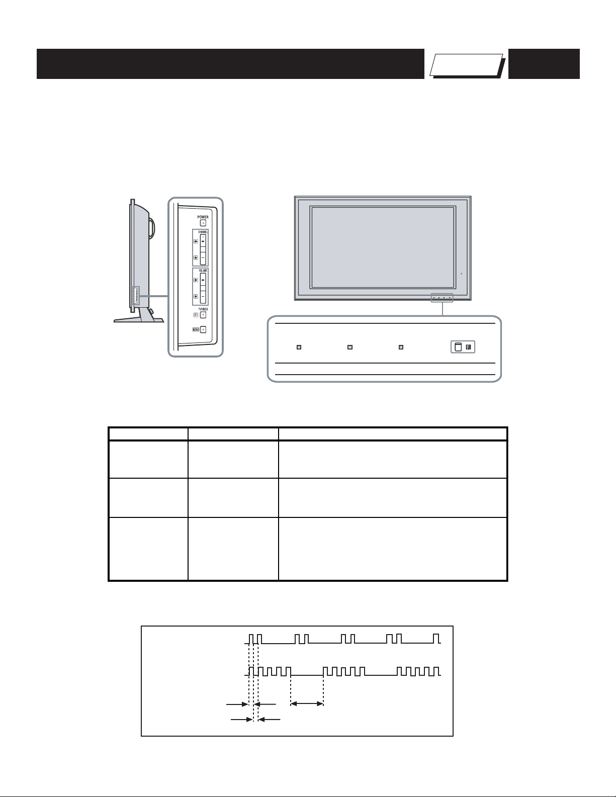
Control Buttons
PIC OFF/TIMER STANDBY POWER
Self Diagnosis
PIC OFF/TIMER STANDBY POWER
Supported model
Description of LED Indictors
LED LED Type Description
POWER LED
STANDBY LED
PIC OFF/TIMER
LED
Display of STANDBY LED Flash Count
*
LED ON 0.3 sec.
LED OFF 0.3 sec.
Green LED
Red LED
Green LED
2 times
5 times
* Light is green when the TV set is on
* Light is red when TV is in PC standby mode.
* Functions as service indicator
* Light is green when Picture Off is activated
* Light is orange when the timer is set
When timer is set, the LED remains lit even
if the TV is turned off.
LED OFF
3 sec.
KDL-70XBR3
10
KDL-70XBR3
Diagnostic Test Indicators
When an error occurs, the STANDBY LED will fl ash a set number of times to indicate the possible cause of the problem. If there is more than one
error, the LED will identify the fi rst of the problem areas. If the errors occur simultaneously, the one that corresponds to the fewest fl ashes is identifi ed
fi rst.
Results for all of the following diagnostic items are displayed on screen. No error has occurred if the screen displays a “000”.
1. TV must be in standby mode. (Power off).
2. Press the following buttons on the Remote Commander within a second of each other:
DISPLAY
The Self Check list displays.
This differs from accessing the Service Menu Adjustments.
Channel 5 Volume -
TV POWER
.
$ %&' ("!"
+ ;
))
)
)
)
&&
&
&
&&
&U"!=&>#
!"##"!"
) )!"##"!"
<"!=&>#
(#""!?
!!###@
""!#JQ
KDL-70XBR3
11
1-1. OVERVIEW
The KDL70XBR3 has considerable weight due to its size. The set weighs approximately 205 lbs (93Kg) with
the base stand and approximately 176 lbs (80Kg) without. Please review the following guidelines before
repairing the set.
NEVER lay the set on the LCD Panel for servicing.
A minimum of two people is recommended to service the set if it is already resting on its stand
and four if the set has been mounted on the wall. This is to ensure that care is taken not to torque
the set which could cause a fracture to the panel.
The preferred position for servicing is mounted on its stand.
Use extreme caution whenever moving the set to avoid damaging the LCD panel.
Whenever possible, always keep at least one arm bracket connected when repairing the set.
1-2. LVDS CABLE REMOVAL
Use the following instructions when replacing the LVDS cables.
KDL-70XBR3
SECTION 1: DISASSEMBLY
KDL-70XBR3
When replacing 1-834-166-11 LEAD WIRE WITH CONNECTOR (LVDS) be sure
the side with the white tape is connected to CN105 on the DEP Board
When replacing 1-834-167-11 LEAD WIRE WITH CONNECTOR (LVDS) be sure
the side with the white tape is connected to theTCON Connector on the LCD
panel.
12

1-3. REAR COVER REMOVAL
1
Remove the outer handles by removing 4 screws, +PSW M5X20
2
Remove 4 screws, +BVST 4X12
3
Remove 1 screw, +BVTP 3X12 TYPE2 IT3
4
Remove 21 screws, +BVTP2 4X16
KDL-70XBR3
Rear Cover
1
Handle
1-4. FAN REMOVAL
(There are 6 Fans per set)
1
Remove the Fan Cushions
2
Remove 4 screws, +PSW M3X8
2
3
4
Cushion
(Fan Spacer)
D.C. Fan
Fan Bracket
Fan Cushion
KDL-70XBR3
2
1
13
1-5. H5 BOARD AND SIDE TERMINAL BRACKET REMOVAL
1
Remove 2 screws, +BVTP2 4X16
2
Remove 2 screws, +BVTP 3X12 TYPE2 IT3
3
Disconnect 2 connectors
3
Side Terminal Bracket
H5 Board
KDL-70XBR3
2
1
1-6. H1 BOARD, H3 BOARD, AND AC INLET REMOVAL
1
Remove 4 screws, +PSW M3X8
2
Remove 2 screws, +PSW M3X12
3
Release the hooks and slide out the H3 Board
4
Disconnect one connector
5
Remove 2 screws, +BVTP2 4X16
6
Release the hooks and slide out the H1 Board
7
Disconnect one connector
H1 Board
7
6
3
4
H3 Board
AC Bracket
AC Inlet
2
1
KDL-70XBR3
Control Button
5
14
1-7. SPEAKER REMOVAL
1
Remove 2 screws, +PWH 4X16
KDL-70XBR3
Speaker (L)
1
1-8. G1P BOARD REMOVAL
Note: If necessary, one Arm bracket can be removed.
1
Remove 4 screws, +PSW M3X8
2
Disconnect 8 connectors
3
Release 5 Spacers
1
Speaker (R)
DEP Board
NOTE: The DEP Board contains critical
adjustment data, therefore, replacement is
not available.
Please contact your service representative
for additional information.
G1P Board
3
Arm
2
KDL-70XBR3
1
15
1-9. AU BOARD AND QT BOARD REMOVAL
1
Remove 7 screws, +BVST 3X8
2
Disconnect 5 connectors
3
Pop off top shield
4
Remove 2 Hex. Washer Nuts.
5
Disconnect 3 connectors
6
Remove 4 screws, +BVST 3X8
7
Remove 4 screws, +BVST 3X8
KDL-70XBR3
Tuner
Shield (Lower)
7
QT Board
4
5
2
3
6
1-10. BEP BOARD AND QM BOARD REMOVAL
1
Remove 2 screws, +BVST 3X8
2
Disconnect 2 connectors
3
Remove 3 screws, +BVST 3X8
4
Disconnect 3 connectors
5
Remove 8 screws, +BVST 3X8
6
Release claw to remove DTT holder
7
Remove 2 screws, +PSW M3X8
8
Remove 4 screws, +BVST 3X8
AU Board
Tuner Shield
(Upper)
1
Digital Shield
(Lower)
6
DTT Holder
QM Board
3
KDL-70XBR3
7
HDMI Terminal
4
2
1
8
5
BEP Board
DIG Shield
(Upper)
16
1-11. G2P BOARD AND F BOARD REMOVAL
1
Disconnect 3 connectors
2
Remove 4 screws, +PSW M3X8
3
Disconnect 2 connectors
4
Remove 4 screws, +PSW M3X8
KDL-70XBR3
1
2
G2P Board
3
4
F Board
1-12. LT3 BOARD, LP3 BOARDS, AND LD3 BOARD (LED BACKLIGHT DRIVERS) REMOVAL
1
Disconnect 1 connector
2
Remove 4 screws, +PSW M3X8
3
Disconnect 1 connector
4
Remove 4 screws, +PSW M3X8
5
Disconnect 6 connectors from LD3-1
6
Remove 4 screws, +PSW M3X8
7
Disconnect 7 connectors from LD3-2
8
Remove 4 screws, +PSW M3X8
9
Disconnect 6 connectors from LD3-3
10
Remove 4 screws, +PSW M3X8
LC3 Board
NOTE: The LC3 Board contains critical
adjustment data, therefore, replacement is
not available.
Please contact your service representative
for additional information.
2
1
LD3 Board-1
LT3 Board
5
6
7
LP3 Board
4
8
3
KDL-70XBR3
LD3 Board-2
9
10
LD3 Board-3
17
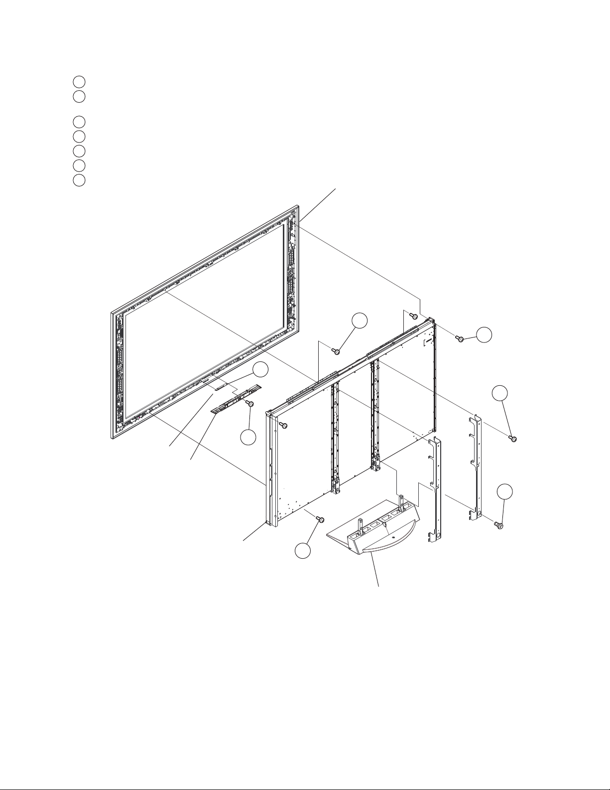
1-13. FRONT CABINET, BASE STAND, AND ARM BRACKET REMOVAL
1
Remove 6 screws from upper stays, +BVTP2 4X16
2
Remove 12 screws from vertical stays on both sides, +BVTP 3X12
TYPE2 IT3
3
Remove 8 screws from lower stay, +BVTP2 4X16
4
Remove 11 screws per arm, +PSW M4X8
5
Remove 4 screws, +PSW M5X12
6
Remove one screw, +BVST 4X12
7
Release claw to remove H4 board
Front Cabinet
KDL-70XBR3
7
6
H4 Board
Under Cover
LCD Panel Assembly
NOTE: Due to the complexity
of this panel, replacement is not available.
Please contact your service representative
for additional information.
1
2
4
5
3
Stand Assembly
KDL-70XBR3
18

2-1. OVERVIEW
Due to the complexity of this set, service adjustments are not available .
KDL-70XBR3
SECTION 2: SERVICE ADJUSTMENTS
KDL-70XBR3
19
3-1. CIRCUIT BOARDS LOCATION
KDL-70XBR3
SECTION 3: DIAGRAMS
3PL
3TL
3CL
noc-T
PED
3DL
2PG
1PG
3DL
F
1H
3DL
BEP
AUP
QM
QT
5H
KDL-70XBR3
3H
4H
20

3-2. PRINTED WIRING BOARDS AND
SCHEMATIC DIAGRAMS INFORMATION
All capacitors are in μF unless otherwise noted. pF : μμF 50WV or
less are not indicated except for electrolytics and tantalums.
All electrolytics are in 50V unless otherwise specifi ed.
All resistors are in ohms. kΩ=1000Ω, MΩ=1000kΩ
Indication of resistance, which does not have one for rating
electrical power, is as follows: Pitch : 5mm
Rating electrical power :
1
/
W in resistance, 1/
4
W and 1/
10
W in chip resistance.
16
: nonfl ammable resistor
: fusible resistor
: internal component
: panel designation and adjustment for repair
: earth ground
: earth-chassis
All variable and adjustable resistors have characteristic curve B,
unless otherwise noted.
Readings are taken with a color-bar signal input.
Readings are taken with a 10MΩ digital multimeter.
Voltages are DC with respect to ground unless otherwise noted.
Voltage variations may be noted due to normal production
tolerances.
All voltages are in V.
S : Measurement impossibility.
: B+line.
: B-line. (Actual measured value may be different).
: signal path. (RF)
Circled numbers are waveform references.
1
/
W
4
KDL-70XBR3
The components identifi ed by shading and ! symbol are critical for safety. Replace
only with part number specifi ed.
The symbol indicates a fast operating fuse and is displayed on the component
side of the board. Replace only with fuse of the same rating as marked.
!
Les composants identifi es per un trame et une marque
securite. Ne les remplacer que par une piece portant le numero specifi e.
Le symbole indique une fusible a action rapide. Doit etre remplace par une
fusible de meme yaleur, comme maque.
NOTE: The components identifi ed by a red outline and a mark contain confi dential
information. Specifi c instructions must be adhered to whenever these components
are repaired and/or replaced.
See Appendix A: Encryption Key Components in the back of this manual.
sont critiques pour la
KDL-70XBR3
21
REFERENCE INFORMATION
KDL-70XBR3
RESISTOR
: RN METAL FILM
: RC SOLID
: FPRD NONFLAMMABLE CARBON
: FUSE NONFLAMMABLE FUSIBLE
: RW NONFLAMMABLE WIREWOUND
: RS NONFLAMMABLE METAL OXIDE
: RB NONFLAMMABLE CEMENT
: ADJUSTMENT RESISTOR
CAPACITOR
: TA TA NTAL U M
: PS STYROL
: PP POLYPROPYLENE
: PT MYLAR
: MPS METALIZED POLYESTER
: MPP METALIZED POLYPROPYLENE
: ALB BIPOLAR
: ALT HIGH TEMPERATURE
: ALR HIGH RIPPLE
COIL
: LF-8L MICRO INDUCTOR
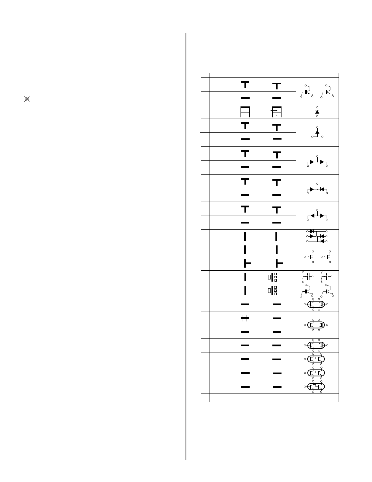
Terminal name of semiconductors in silk screen
printed circuit ( )
Device Printed symbol Terminal name
Transistor
1
Transistor
2
3
Diode
4
Diode
Diode
5
Diode
6
Diode
7
8
Diode
Diode
9
Diode
0
Diode
!¡
Diode
!™
Transistor
!£
(FET)
Transistor
!¢
(FET)
Transistor
!?
(FET)
Transistor
!§
Transistor
!¶
Transistor
!•
Transistor
!ª
Transistor
@º
Transistor
@¡
Transistor
@™
Transistor
@£
Discrete semiconductot
–
(Chip semiconductors that are not actually used are included.)
*
Collector
Base
Collector
Base
Cathode
Cathode
Anode
Cathode
Anode
Common
Anode
Common
Anode Cathode
Common
Anode
Common
Anode Anode
Common
Cathode
Common
Cathode
Anode
Anode
Cathode
Drain
Drain
B1 E1
C2
B2 C1E2
B2 E2
C1
B1 C2
E1
B2 E2
C1
B1 C2E1
B2 E2
C1
B1 C2E1
E2
B1 E1
C2
(B2)
E1
B1
C1
(B2)
E1
E2
C2
Emitter
Emitter
Anode
(NC)
(NC)
Cathode
Anode
Cathode
Cathode
Cathode
Anode
Anode
Source
Gate
Source
Gate
Source
Drain
Gate
Emitter
Collector
Base
C1(B2)
E2
C2
B1
C1
Circuit
D
G
D
S
B1
B1
B1
B1
B1
B1
D
G
S
S
D
G
C1
E1
C1
E1
E1
C1
E2
C1
C1
G
S
C2
B2
E2
C2
B2
E2
E2
B2
C2
C2C1(B2)
E2
E2E1(B2)
C2
C2E1(B2)
C2
Ver.1.6
KDL-70XBR3
22
KDL-70XBR3
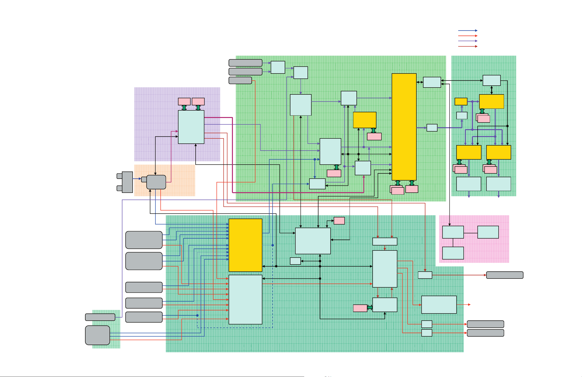
3-3. BLOCK DIAGRAMS
SYSTEM BLOCK DIAGRAM
ANT
SW
QM
QT
TU
I2C
DDR FLASH
IF
ATI
Gfx
SPDIF
I2S
HDMI 1
HDMI 3
A-AU
EQ
EQ
HDMI
Rx
Sil9011
PC
1080p
ADC
CCPXA
Main
SDRAM
Bus
SW2
DRC
MFV2.5
SDRAM
Bus
SW1
I2C
I2C
UART
IFP2S
DDR
DDR
FLASH
DEM
LVDS
Tx
B
UART
UART
UART
Format
Conv.
LVDS
Rx
DDR
DDR
Lance
LVDS
Tx
Analog Video Signal
Analog Audio Signal
Digital Video Signal
Digital Audio Signal
DE
HGM
Axilleus
DDR
DDR
Lance
DDR
DDR
LVDS
Tx
I2C
HDMI 2
V2
V1(S/CV)
V3(CV)
Component1
Component2
PC
VIDEO
SW
CXA2240
Audio
SW
CXA2188Q
UART
RTC
I2C
TVM
Saiph
I2C
I2C
NVM
UART
SRAM
SEL
MAP
4400A
Delay IC
CXD9826
A
LBM PLD
Sensor
Buff
D-AMP
M61571AFP
MUTE
MUTE
I2C
Photo
To
Panel
To
SP
L/R Out
Head Phone
To
Panel
LC
Opt. Out
KDL-70XBR3
23
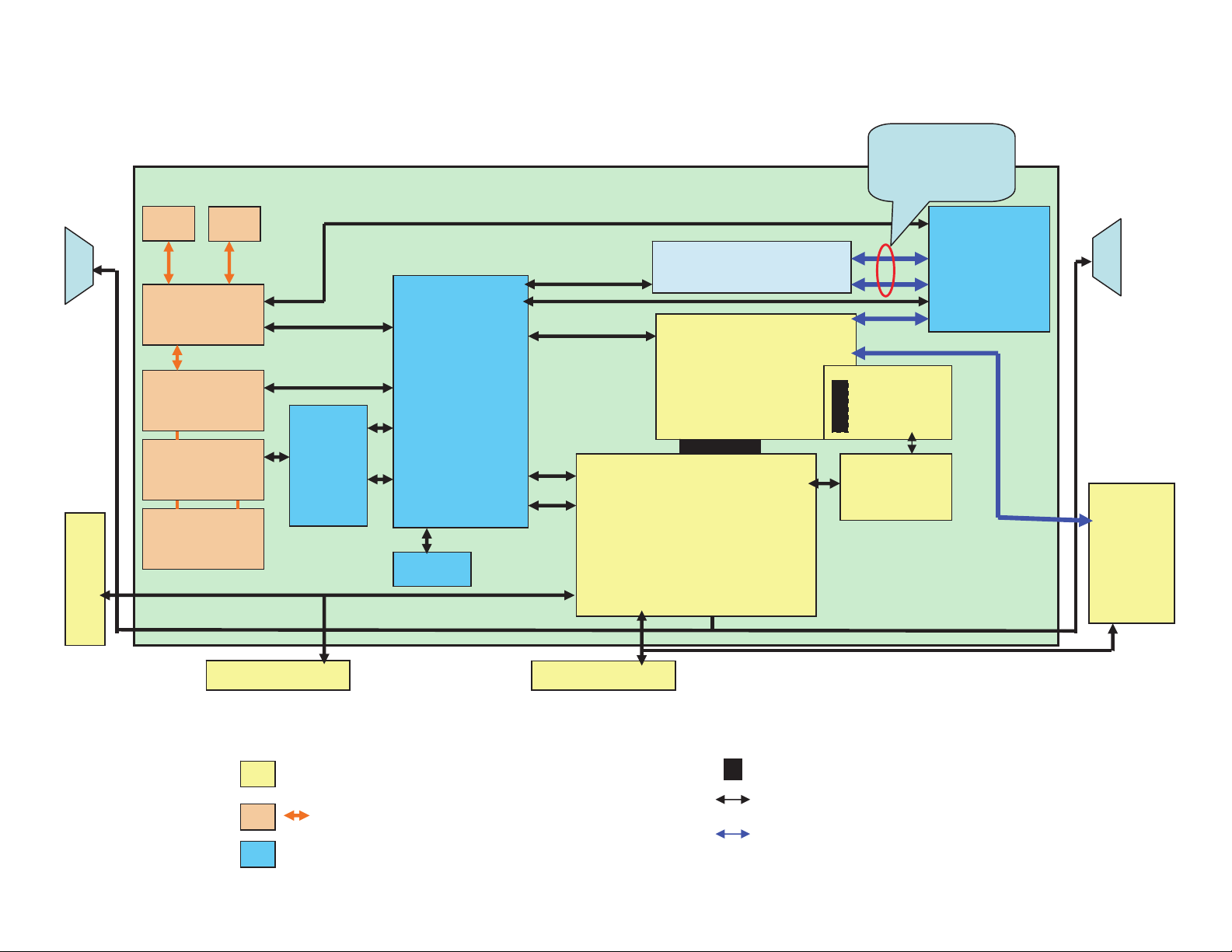
CONNECTIONS DIAGRAM
KDL-70XBR3
Additional
LVDS
S
P
H1
CN3001
LT3
LC3
LD3
LD3
LD3
LP3
H3
CN6902
G2
CN3201
CN6901
CN6930
CN6501
CN6403
CN6400
CN6401
CN6402
CN6018
F
G1
CN6551
CN6555
CN6550
CN6552
H4
CN9003
CN9002CN6503
CN9001
CN9006
CN3301
T-con
CN4000
AUP
BEP
CN4002
CN9007
CN8801
CN4001
CN9004
CN5900
CN4501
CN7306
CN7803
QM
CN7802
CN7800
CN1007
CN7700
CN7701
CN1007
CN1002
CN1051
QT
DEP
S
P
CN1301
H5
CN3100
KDL-70XBR3
Same function FIX chassis
Included in LED BL Module
New for FIXP chassis
B to B
Conventional
LVDS
PWB
24
3-4. SCHEMATICS AND SUPPORTING INFORMATION
AUP BOARD SCHEMATIC DIAGRAM (1 OF 7)
KDL-70XBR3
| 32 | 22 | 12 | 02 | 91 | 81 | 71 | 61 | 51 | 41 | 31 | 21 | 11 | 01 | 9 | 8 | 7 | 6 | 5 | 4 | 3 | 2 | 1
A
—
B
—
C
—
D
—
E
—
F
—
G
—
H
—
I
—
J
—
K
—
PC
BLK
15P
CN8001
VIDEO1
VIDEO3
V
L
R
Y
GRN
Cb
BLU
Cr
RED
L
WHT
R
RED
Y
GRN
Cb
BLU
Cr
RED
L
WHT
R
RED
R8005
47
1/10W
RN-CP
R8006
47
1/10W
RN-CP
S
34
12
V
L
R
J8004
J8002
1
2
3
4
5
6
7
8
9
10
11
12
13
14
15
16
17
18
19
20
FB 8003
FB 8004
FB 8002 0uH
PS8001
0.4A
R8001
330k
R8002
R8003
330k
330k
R8004
330k
VD 8013
VD 8014
V1_SSWV1_SSW
VD 8015
D8005
MA 8100-T X
D8006
MA 8100-T X
R8025
220
1/10W
RN-CP
5%
C8007
47
16V
C8008
47
16V
COMP1_V_IN
COMP1_LR_IN
COMP3_V_IN
COMP3_LR_IN
V1_Y
V1_C
V1_V
V1_L
V1_R
V1_IN
V1_LR_IN
VD 8016
MA 8100-T X
V3_L
V3_L
D8007
MA 8100-T X
V3_R
D8008
V3_LR_IN
V3_V
R8059
R8060
R8061
V5V
R8130
0
CHIP
1608
C8064
0.1
16V
B
1608
IC 8002
AD A4861-3Y R Z- RL 7
L8002
10uH
7654321
C8028
V5V
120
6.3V
V1_IN
OP-AMP
PD1
PD2
PD3
VCC
IN+1
IN-1
OUT1 OUT3
COMP1_V_IN
COMP3_V_IN
V9V
R8069
0
CHIP
1608
COMP
PC_V _IN
PC_R
0
PC_G
0
PC_B
0
C8024
CCP_Y
CCP_CR
CCP_CB
47
R8076
C8026
470
0.1
1/10W
RN-CP
Y
0.5%
R8077
56
CB
1/10W
RN-CP
0.5%
CR 1.7
OUT2
IN-2
IN+2
VEE
IN+3
IN-3
C8027
0.1
16V
B
1608
MAIN_CV/Y
C8029
0.1
16V
B
1608
R8092
330k
C8030
16V
2012
V1_C
V1_Y
V1_V
R8078
470
1/10W
RN-CP
14 13 12 11 10 9
0.5%
R8080
56
1/10W
RN-CP
0.5%
C8055
16V
X7R
1005
R8079
470
1/10W
RN-CP
0.5%
8
R8081
56
1/10W
RN-CP
0.5%
MAIN_C
1
R8087
B
R8091
330k
R8093
330k
R8084
1/10W
RN-CP
0.5%
R8095
R8101
10
R8086
R8094
R8096
R8097
R8098
R8102
R8103
COMP3_CB
COMP3_Y
COMP3_CR
1/10W
RN-CP
R8099
R8100
R8104
R8105
R8106
330
R8085
1/16W
100
100
5%
100
100
100
100
100
100
100
100
C8044
2.2
C8051
COMP1_CB
COMP1_Y
COMP1_CR
C8031
1/16W
C8033
C8037
1/16W
1/16W
100
100
1/16W
1/16W
100
1/16W
100
1/16W
100
1/16W
16V2.2
R8082
10
1/10W
RN-CP
0.5%
R8088
10
1/10W
RN-CP
0.5%
2.4
R8089
22
1/10W
RN-CP
1.7
0.5%
Q8004
2SA 1576A-T 106-Q R
BUFFER
16V2.2
2012
C
1/16W
C8032
2.2
C8036
2.2
1
10V
C8034
1
10V
C8035
1
10V
16V2.2
2012
C
1/16W
C8038
2.2
C8039
2.2
C8040
1/16W
C8041
1/16W
2.2
C8042
1/16W
2.2
C8045
2.2 C
16V
C8046
1/16W
2.2
C8047
2.2
C8048
2.2
C8049
2.2
C8050
2.2
100
C8043
R8107
1/16W
0.1
16V
100
R8108
201216V
C
1/16W
R8110
2012
C
C8052
2.2
C
C8053
2.2
C
C8054
2.2
C
16V
R8083
330
1/10W
RN-CP
5%
R8090
330
1/10W
RN-CP
5%
2SA 1576A-T 106-Q R
2.4
2.4
201216V
C
2.4
201216V
C
3.6
3.6
3.6
3.6
3.6
201216V
C
3.6
201216V
C
16V2.2
2012
C
201216V
C
201216V
C
2012
201216V
C
201216V
C
201216V
C
201216V
C
201216V
C
3.6
3.6
100
3.6
1/16W
R8111
201216V
R8112
201216V
R8113
2012
R8115
10
1/10W
RN-CP
0.5%
2.4
2SA 1226-T1E 3E 4
2.4
1.7
Q8005
BUFFER
91
92
93
94
95
96
97
98
99
100
101
102
103
104
105
106
107
108
109
110
111
112
113
114
115
116
117
118
119
120
100
100
100
R8117
330
1/10W
RN-CP
5%
2.4
R8116
22
2SA 1226-T 1E 3E 4
1/10W
RN-CP
1.7
0.5%
Q8006
BUFFER
R8121
22
1/10W
RN-CP
0.5%
CV/Y
C_OUT1_2
NC
CV_OUT1_2
B_IN14
G_IN14
R_IN14
NC
CLP_CR2
CLP_CR1_1
CLP_CR1_2
FBLK _IN3
SC _B /C /CB /B _I N1 3
SC _G /Y /Y /G_ IN 13
SC _R /C V /CR /R _I N13
FBLK _IN2
3.6
SC _B /C /CB /B _I N1 2
3.6
SC _G /Y /Y /G_ IN 12
3.6
SC _R /C V /CR /R _I N12
VCC_IN
FBLK _IN1
3.6
SC_B/C/CB/B_IN11
3.6
SC _G /Y /Y /G_ IN 11
3.6
SC _R /C V /CR /R _I N11
MD/S2-4
3.6
C/CB/B_IN10
3.6
Y/Y/G_IN10
3.6
CV/CR/R_IN10
S1-4
C/CB/B_IN9
Y/Y/G_IN9
CV/CR/R_IN9
GND_IN
1/16W
1/16W
1/16W
VCCFB_OUT
C/CB/B_IN8
Y/Y/G_IN8
CV/CR/R_IN8
123456789101112131415161718192021222324252627282930
3.6
3.6
R8118
1/10W
RN-CP
Q8007
BUFFER
FBLK _OUT
MD/S2-3
3.6
10
0.5%
R8122
16V
2.2
C8057
1/16W
100
2012
C
R8119
1/10W
RN-CP
0.5%
VCC5R_OUT1
C/CB/B_IN7
22
R8123
16V2.2
R8114
1/10W
RN-CP
2SA 1226-T 1E 3E 4
C/CR/R _OUT1_1
Y/Y/G_IN7
3.6
3.6
1/16W
1/16W
R8124
100
100
16V
2012
2012
2.2
C
C
C8059
C8058
330
5%
2.4
VCC5G_OUT1
CV/CR/R_IN7
0.1
Q8008
BUFFER
CV /Y /G _O UT 1_1
S1-3
3.6
C8065
120
6.3V
C8056
1
16V
B
2012
R8120
22
1.7
1/10W
RN-CP
0.5%
C8070
0.1
16V
B
1608
VCC5_OUT2
VCC5B_OUT1
C/CR/R _OUT2
CV/Y/G_OUT2
C/CB/B_OUT1_1
C/CB/B_IN6
Y/Y/G_IN6
CV/CR/R_IN6
MD/S2-2
C/CB/B_IN5
3.6
3.6
3.6
1/16W
201216V
201216V
100
C
C
2.2
C8060
1/16W
100
R8126
2012
R8138
201216V
C
2.2
C8075
16V
2.2 C
2.2
C8061
C8074
1/16W
1/16W
100
100
V2_V
R8127
R8141
R8135
68k
1/16W
CHIP
5%
C8067
0.1
16V
1608
C/CB/B_OUT2
IC 8003
CX A 2240R- TL
VIDEOSW
Y/Y/G_IN5
3.6
3.6
201216V
201216V
C
C
C8076
C8077
2.2
2.2
1/16W
100
R8142
V9V
L8004
10uH
C8066
47
C8068
16V
0.1
16V
B
1608
V5V
R8136
68k
1/16W
CHIP
5%
B
C8069
0.1
16V
B
1608
Y_PH2
Y_PH1
GND9_ OUT
GND5_ OUT
CV/CR/R_IN5
CV/Y_OUT3
S1-2
C/CB/B_IN4
Y/Y/G_IN4
CV/CR/R_IN4
3.6
3.6
3.6
1/16W
100
R8143
3.6
2012
201216V
201216V
C
C
C8079
C8080
C8078
16V
2.2 C
2.2
2.2
1/16W
1/16W
1/16W
100
100
100
R8145
R8146
R8144
4.7
R8137
100
1/16W
CHIP
CV_SAG
CV_OUT5
VCC9_OUT
CV/Y_OUT4
S2-1
CV3
CV2
CV1
3.6
3.6
1/16W
1/16W
100
100
R8139
16V
R8140
2.2
2.2
2.2
16V
16V
C8071
C8072
C8073
1/16W
100
R8147
V3_V
TV_M_V
R8151
1/16W
RN-CP
0.5%
NC
S1-1
4.0
1k
C8093
Y_SAG
CV/Y_OUT5
IN1_L 3
IN1_V /L2
10V
0.47
Q8011
2SC 4081T106R
DATA_SL ICER _MAIN
NC
C_OUT5
EXT_CLK/X’TAL
IN1_H/L1
IN1_SW
1.0
1.0
10V
0.47
C8094
1/16W
1/16W
100
100
R8159
R8160
616263646566676869707172737475767778798081828384858687888990
ADR
DC_OUT
VCC5H_OUT
SELV _OUT2
SELH_OUT2
SELV _OUT1
SELH_OUT1
GND5H_OUT
PS_HV CS
VCC_DEF
SYNC_IN2
SYNC_OUT2
SYNC_IN1
SYNC_OUT1
GND_DEF
IN3_H/L1
IN3_V /L2
IN2_H/L1
IN2_L 3
IN2_V /L2
PC_ID
V_PH2
H_PH2
V_PH1
H_PH1
IN4_H
IN4_V
IN3_SW
IN3_L 3
IN2_SW
1.0
C8095
1/16W
100
R8161
V5V
L8005
10uH
C8097
C8098
120
0.1
6.3V
16V
B
1608
R8156
47
4.7
SCL
SDA
IREF
10V
0.47
1/16W
60
4.7
R8157
59
58
57
56
55
54
53
52
51
50
49
48
47
46
45
44
43
42
41
40
39
38
37
36
35
34
33
32
31
0.0
1.0
3.3
2.9
C8085
C8086
1.0
1.0
C8091
1.0
0.47
10V
1.0
1.0
C8087
C8092
0.47
10V
C8096
0.47
10V
R8158
10k
1/16W
RN-CP
009:16H
1/16W
PC_ID
PC_SY NC_DE T
1
10V
0.01
C8088
C8089
4.7
10V
C8090
4.7
10V
R8166
R8167
R8168
47
1608
B
B
16V
B
10V1
1608
B
0.01
16V
C8100
0.1
10V
B
1005
100
1/16W
100
1/16W
100
1/16W
SCL_DEV _5V
SDA_DEV_5V
PC_SY NC_IN
PC_H_I N
PC_V _IN
4MHz
X8001
C8101
10V
I2C_DEV_5V
0
R8165
47
C8102
C8103
0.1
10V
B
0.1
L8006
10uH
Q8012
SI2301BDS-T1
2012
B
25V
1
C8104
S
STBY 5V
R8169
10k
1/16W
CHIP
5%
R8170
10k
1/16W
CHIP
5%
OPTOUT
LINE_LR_OUT
Q8013
DT C144E UA -T 106
LINE_L
LINE_R
FB 8006
0uH
VSW_PW_CTRL
D5V
C8062
100
6.3V
VIN
GND_1
FB 8008
0uH
GND_1
VCC
GND
J8005
L
L
R
R
J8003
C8063
0.1
10V
B
1005
VD8017
FB 8007
0uH
VD8018
B
16V
R8011
220
1/10W
5%
R8010
0
CHIP
VD8001
VD 8002
VD 8003
VD 8004
VD 8005
VD 8006
C8009
47
C8010
47
VD 8007
VD 8008
VD 8009
VD 8010
VD 8011
VD 8012
8011
C
47
C8012
47
0uH
0uH
R8013
1/10W
RN-CP
R8028
220
R8029
R8034
R8035
220
R8040
220
R8041
220
R8014
1/10W
RN-CP
220
5%
R8012
R8015
1/10W
RN-CP
220
220
R8017
220
220
1/10W
RN-CP
5%
5%
R8020
R8016
220
220
1/10W
1/10W
RN-CP
RN-CP
5%
5%
220
5%
220
5%
0
R8021
CHIP
R8030
220
COMP1_CB
R8031
220
COMP1_CR
R8036
220
MA 8100-T X
MA 8100-T X
R8037
220
COMP3_CB
R8042
220
COMP3_CR
R8043
220
MA 8100-T X
MA 8100-T X
R8018
220
1/10W
RN-CP
5%
R8019
330k
5%
1/16W
CHIP
R8023
330k
5%
1/16W
CHIP
COMP1_Y
COMP1_L
D8009
COMP1_R
D8010
COMP3_Y
COMP3_L
D8011
COMP3_R
D8012
R8022
220
5%
R8038
220
5%
R8045
220
5%
MA 8100-T X
C8005
47
16V
C8006
47
16V
R8024
220
1/10W
RN-CP
5%
R8026
330k
5%
1/16W
CHIP
R8027
330k
5%
1/16W
CHIP
R8032
220
5%
R8033
220
5%
R8039
220
5%
R8044
220
5%
D8004
R
G
B
H
V
L
—
M
—
N
—
O
—
P
J8001
FB 8001
0uH
R
L
R8008
330k
1/10W
RN-CP
R8052
47
1/10W
RN-CP
R8062
47
1/10W
R8055
10k
1/10W
RN-CP
D8001
D8002
MA 8056-T X
C8004
16V
D8003
MA 8056-T X
5%
10
R8009
330k
1/10W
RN-CP
MA 8056-T X
R8053
2.2k
5%
1/10W
RN-CP
C8002
10
16V
MA 8100-T X
D8014
R8054
2.2k
1/10W
RN-CP
R8057
CHIP
R8058
CHIP
D8015
MA 8100-T X
D8013
M1M A152W K -T 1
PC_AU_R
0
PC_AU_L
0
R8056
1/10W
RN-CP
10k
D3.3V
C8014
0.1
16V
B
1608
PC_LR _IN
RN-CP
EEPROM
M24C 02-WM N6T (B )
IC 8001
E0
1
E1
2
E2
3
4321
VSS5SDA
4
8
8765
VCC
7
WC
6
SCL
5%
100
R8065
1/10W
RN-CP
R8063
4.7k
1/10W
RN-CP
3.1
0.0
Q8001
DTC114EUA-T106
SW
WRT_PRT
D8018
HN1D03FU-TE85R
FB 8005
0uH
C8015
16V
1608
R8067
470
1/16W
CHIP
5%
R8068
470
1/16W
CHIP
5%
R8070
Q8002
2PC4081R -115
C8017
C8016
0.1
0.01
47
16V
6.3V
B
B
1608
C8018
47p
50V
CH
1608
C8020
4.7
16V
X7R
3216
C8021
4.7
16V
X7R
3216
C
8019
4700p
50V
B
1608
M1M A152W K -T 1
Q8003
2PC4081R -115
M1M A152W K -T 1
D8019
D8020
1/16W
CHIP
18k
5%
C8022
0.01
16V
R8071
1/16W
CHIP
C8023
0.01
16V
X7R
X7R
18k
5%
R8072
R8073
R8074
CHIP
R8075
CHIP
PC_SY NC_IN
PC_H_IN
0
PC_V_I N
PC_SY NC_OUT
0
0
PC_H_O UT
PC_V _OUT
0
AUP MOUNT (1/7)
VIDEO SWITCH
INPUTS
A- 1218- 907-A<F IX P>A UP-P 1
KDL-70XBR3 25
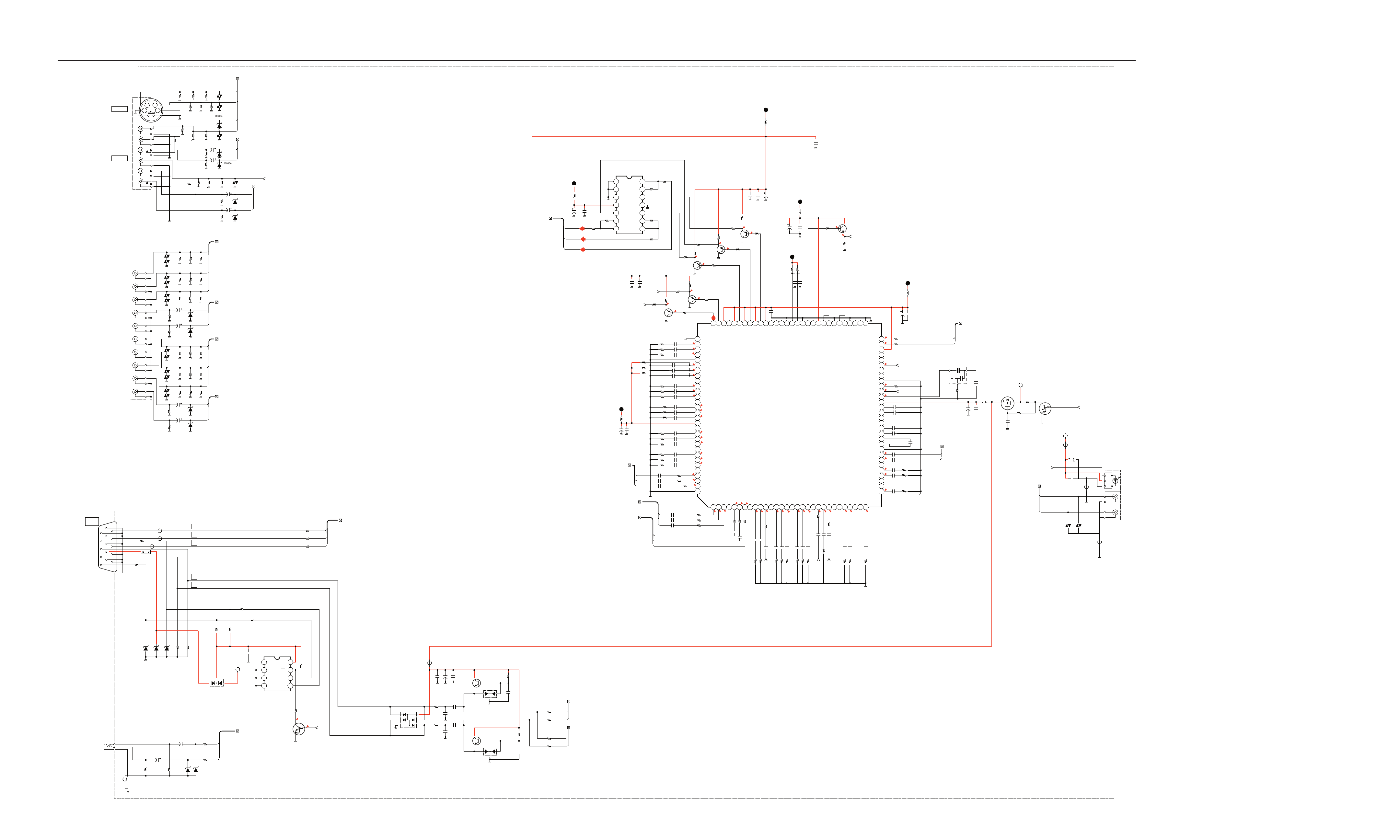
AUP BOARD SCHEMATIC DIAGRAM (2 OF 7)
A
—
STBY3.3V
KDL-70XBR3
62 | 52 | 42 | 32 | 22 | 12 | 02 | 91 | 81 | 71 | 61 | 51 | 41 | 31 | 21 | 11 | 01 | 9 | 8 | 7 | 6 | 5 | 4 | 3 | 2 | 1
AUP BOARD WAVEFORMS
6
00
(
B
—
C
—
D
—
E
—
F
—
G
—
H
—
I
—
J
—
K
—
L
—
M
—
N
—
O
TO H3
CN3201
AND
TO H1
CN3001
TO G1P board
CN6503
TO G1P board
CN6552
GND
STBY3.3V
LED_1
LED_2
LED_3
LED_4
LED_5
GND
SIRCS
D3.3V
BL_IN
D3.3V
GND
LEAN1
POWER_SW
GND
KEY
GND
CN9001
20P
RLY_ON
PANEL_DET
BACK_LIGHT
DIMMER
GND
AC_RLY
PFC_DET(AC_DET)
+B_OVP
STBY_5V
GND
GND
NC(18V)
CN9002
13P
WHT
GND
GND
AUDIO_VCC
AUDIO_VCC
CN9003
4P
6
00
6
6
00
00
(
(
(
C9002
1000p
50V
CH
1005
1
2
3
4
5
6
7
8
9
10
11
NC
12
13
14
15
NC
16
17
18
19
20
1
2
3
4
5
6
R9005
0
7
8
9
10
11
12
NC
13
GND_1
1
2
3
4
C9001
1000p
50V
CH
1005
FB9001
FB9002
R9001
CHIP
R9006
C9004
1000p
1005
0
0
50V
CH
0uH
0uH
FB9005
0uH
FB9006
0uH
R9002
R9003
R9004
CHIP
FB9010
0uH
C9003
1000p
50V
CH
1005
0
0
0
FB9003
FB9004
0uH
FB9007
0uH
FB9008
0uH
FB9009
0uH
0uH
C9005
1000p
50V
CH
1005
GND_1
SIRCS
BL_IN
POWER_SW
KEY1
AUDIO_VCC
STBY_LED
PMUTE_LED
ON_TIMER_LED
REC_LED
POWER_LED
D3.3V
INV_FAIL
BL_ON
DIMMER
AC_RLY
PFC_DET
+B_OVP
STBY5V
MAIN_H_SYNC
C9007
56
DIC_11V
GND
A1
GND
A2
11V
D3.3V
FB9012
0uH
C9032
0.1
10V
B
1005
8765
TMP75AIDR
IC9002
TEMP SENSOR
4321
COMP
I2C_DEV
I2C_DIC
DIC_SCL
DIC_SDA
CCP_Y
CCP_CB
CCP_CR
DAT_DE
HDMI_BCK
HDMI_LRCK
HDMI_DA1
DL_MODE
PC_V_IN
SDA_DEVICE
SCL_DEVICE
IFP LOG
WEM_LOG
0.0
IC9003
0.0
CH0
INH
VCC
OUT2
A1
I2C_DE
0.0
CH1
VEE
GND A
4321
8765
0.0
1/16W
R9078
CHIP5%1k
3.3
100k
R9079
1/16W
D3.3V
R9080
10k
1/16W
CHIP
5%
Q9013
MUN2213T1
CHIP
VSYNC_SEL
5%
I2C_HDMI
HDMI_SDA
HDMI_SCL
C9035
0.01
16V
X7R
1005
HDMI_CE_B
HDMI_INSEL2
0.0
sw
HDMI_CE
WRT_PRT
D5V
0uH
FB9013
GND_1
IC9004
TC7W53FU(TE12R)
LOGIC GATE
IFP_VS
0.0
R9075
100
1/16W
CHIP
5%
HDMI_INSEL2_B
R9072
100
1/16W
CHIP
5%
FB9014
C9033
1000p
50V
CH
1005
JL9044
0.0
4321
LOGO
STBY5V
0uH
CLK_DE
DAT_DE
8765
VCC
COM
0.0
TC7W08FU(TE12R)
A2
B2
OUT1
VEE B1
0uH
FB9015
C9034
1000p
50V
CH
1005
R9069
22
1/16W
CHIP
R9067
22
SIDE_LR_IN
0
CHIP
R9063
R9066
1/16W
CHIP
0
R9065
SIDE_LR_IN_L
SIDE_LR_IN_R
0
CHIP
TV_M_V
CHIP
0
R9068
CHIP
R9070
HDMI_INSEL2_B
R9071
100
1/16W
CHIP
5%
V2_V
0
CHIP
V5V
10uH
R9048
4.7k
1/16W
CHIP
5%
1005
1M
CHIP
5%
0.1
C9023
5%
5%
5%
CHIP
1/16W
L9002
16V
1005
33
CHIP
R9051
1/16W
150
CHIP
R9052
1/16W
Q9008
2SA1235TP-1EF
R9049
1M
1/16W
CHIP
5%
C9024
100k
R9050
0.1
10V
B
1005
B
50V
470p
1005
C9025
001:17B
2SA1576A-T106-QR
R9053
C9026
4.7k
1/16W
CHIP
5%
R9054
470
1/16W
CHIP
5%
0.047
10V
B
1005
TU_V_OUT
Q9009
R9055
ANTSW_MAIN
5%
100
CHIP
1/16W
5%
2.2k
CHIP
1/16W
Q9010
2SA1235TP-1EF
C9027
1000p
50V
CH
1005
R9056
R9057
1/16W
CHIP
5%
1k
L9003
10uH
6.3V
100
V5V
C9028
A9V
L9004
10uH
C9030
C9029
47
16V
0.1
16V
X7R
1005
Q9011
2SC3052EF-T1-LEF
R9059
2.2k
1/16W
RN-CP
0.5%
0.5%
R9058
CHIP
R9061
4.7k
1/16W
CHIP
5%
0
R9060
100
1/16W
CHIP
5%
FB9011
HP_DET
0uH
2SA1235TP-1EF
HP_LR_OUT
HP_R
0
CHIP
R9062
Q9012
HP_L
D3.3V
1608
NJM4558V-TE2
4321
5%
5%
TV_M_L_IN
5%
1/16W
0
IC9001
C9013
R9026
22k
B
6.3V
1
C9015
8765
B
10V
0.22
1608
C9014
2SA1235TP-1EF
D9001
MC2836
R9028
15k
B
1/16W
50V
1005
CHIP
2200p
5%
SCL_DEVICE
AFT_MAIN
TU_V_OUT
47
R9031
1/16W
R9027
0
1k
5%
CHIP
R9033
1/16W
47k
0.5%
RN-CP
R9034
1/16W
R9035
R9036
C9016
RB501V-40TE-17
D9002
C9019
R9029
2200p
1M
1/16W
50V
CHIP
B
5%
1005
Q9005
R9030
15k
1/16W
CHIP
5%
SDA_DEVICE
AGC_MUTE
47
5%
CHIP
R9032
1/16W
5%
CHIP
R9037
0
15k
1/16W
3.3k
1/16W
2.2
10V
I2C_DEV
CHIP
CHIP
B
5%
2.2k
R9038
5%
5%
2012
CHIP
1/16W
CHIP
1/16W
47k
L9001
10uH
22
10V
C9009
C9008
56
C9010
0.1
16V
1005
Q9001
2SA1576A-T106-QR
B
16V
0.01
1005
C9011
5%
4.7k
CHIP
R9007
1/16W
V_DET
Q9002
2SC3052EF-T1-LEF
R9008
100
1/16W
CHIP
5%
5%
0.5%
CHIP
0.5%
RN-CP
1/16W
CHIP
0
R9012
68k
RN-CP
R9009
1/16W
C9012
4.7
50V
3.3k
R9010
1/16W
2SA1235TP-1EF
R9011
JL9023
5%
39k
0.5%
4.7k
RN-CP
CHIP
R9013
1/16W
Q9003
CHIP
1/16W
1/16W
5%
CHIP
1/16W
100
R9016
68k
R9014
5%
22k
R9015
TV_M_LR_IN
22k
0.5%
RN-CP
R9019
1/16W
22k
0.5%
RN-CP
R9020
1/16W
R9021
3.3k
1/16W
CHIP
5%
Q9004
2SC3052EF-T1-LEF
5%
CHIP
1/16W
10k
R9024
220k
R9017
1/16W
R9023
100k
1/16W
CHIP
33k
R9018
1/16W
TV_M_R_IN
R90220R9025
CHIP
5%
CHIP
0.5%
R9039
3.9k
1/16W
CHIP
5%
R9041
5%
CHIP
RN-CP
1/16W
R9040
22
10V
C9022
2SA1576A-T106-QR
0
R9042
C9020
33k
R9043
C9021
4700p
16V
B
1005
R9044
2.7k
1/16W
CHIP
5%
5%
22k
CHIP
1/16W
5%
10k
CHIP
R9045
1/16W
0.5%
RN-CP
1/16W
22k
R9047
Q9007
B
2.2
6.3V
1608
Q9006
2SA1235TP-1EF
R9046
1/16W
CHIP
R9083
I2C_DE
CLK_DE
I2C_IFP
CHIP
CHIP
R9089
CHIP
0
IFP_SDA
IFP_SCL
R9090
0
V5V
MAIN_CV/Y
MAIN_C
0
CHIP
CHIP
R9091
0
CCDM_H
CCDS_H
IFP_USB
USB_UDP
USB_UDM
IFP_UDP
IFP_UDM
IFP_VBUS
R9087
R9088
PC_B
PC_G
PC_R
CHIP
R9095
0
R9096
R9094
0
R9084
0
R9085
0
R9086
CHIP
0
FL9001
0
0
R9099
0
EMI
CHIP
CHIP
CHIP
CHIP
G
GND_1
R9097
0
0
R9098
0
R9101
CHIP
CHIP
33
1
2
3
4
CHIP
R9100
CHIP
33
A3
11V
A4
11V
A5
11V
A6
GND
A7
GND
A8 B8
VIDEO5V
A9 B9
VIDEO5V
A10 B 10
GND
A11 B 11
GND
A12
MAIN_CV/Y
A13
MAIN_C
A14
GND
A15 B 15
GND
A16 B 16
SUB_C
A17 B 17
SUB_Y/CV
A18 B 18
GND
A19 B 19
GND
A20 B 20
MAIN_Y
A21 B 21
MAIN_CB
A22
MAIN_CR
A23
GND
A24
GND
A25
FE_CVBS
A26
FE_Y
A27
FE_C
A28 B 28
GND
A29 B 29
GND
A30 B 30
DE_SCL
A31 B 31
DE_SDA
A32
GND
A33
GND
A34 B 34
HDMI_BCK
A35
HDMI_LRCK
A36
HDMI_DATA
A37
DL_MODE
A38
IFP_VS
A39
GND
A40
PC_B
A41
PC_G
A42
PC_R
A43
D5_CB
D5_Y
A45
D5_CR
A46
GND
IFP_SDA
A48 B 48
IFP_SCL
A49 B 49
GND
A50 B 50
TVM_SDA(SUBC)
A51 B 51
TVM_SCL(SUBC)
A52
GND
A53
HDMI_SDA
A54
HDMI_SCL
A55
GND
A56
FE_SDA
A57
FE_SCL
A58
GND
A59
MAIN_HS(UC)
A60
SUB_HS(UC)
A61
GND
A62
FE_USB_UDP_JG(UC)
A63
FE_USB_UDM_JG(UC)
A64
WE_USB_UDP
A65
WE_USB_UDM
A66
WE_USB_VBUS
A67
BE_UART_JG
A68
DIC_SCL
A69
DIC_SDA
A70
GND_1 GND_1
DE_UART_TX_JG(SOT0)
DE_UART_RX_JG(SIN0)
DE_UART_CK_JG(SCK0)
DE_FLSH_MODE(MD2)
CN9007
140P
BLK
TO BEP
CN4002
GND
GND
GND
FAN_ERR
FAN_DRIVE
DIMMER
BL_ON
INV_FAIL
PFC_DET
BL_IN
GND
GND
PC_H
PC_V
GND
MAIN_YS
GND
GND
HDMI_L
HDMI_R
GND
GND
FE_L
FE_R
GND
GND
HDMI_AU_SPDIF(L)
SPDIF
GND
AU_BCK
AU_LRCK
AU_DATA0
AU_DATA1(Jpn)
AU_DATA2(Jpn)
SUB_ON
SET_ON
BE_BOOT
BE_RST
BE_WDT
DE_RST
TILT_DET
M_UART_TX_BE
M_UART_RX_BE
M_UART_TX_FE
M_UART_RX_FE
FE_RST
HDMI_INT
HDMI_50/60
HDMI_INCE
HDMI_INSEL
HDMI_HPG_DET1
HDMI_HPG_DET2
HDMI_WRT_PRT
HDMI_CEC2
HMHDM_RST
HDMI_INSEL_2
GND
DE_FLASH_WR(P61)
DE_USB_VBUS
DE_USB_UDP
DE_USB_UDM
U2_TX(Jpn)/FE_LO
B1
B2
11V
B3
11V
B4
11V
B5
11V
B6
B7
B12
B13
B14
B22
B23
B24
B25
B26
B27
B32
B33
B35
B36
B37
B38
B39
B40
B41
B42
B43
B44A44
B45
B46
B47A47
B52
B53
B54
B55
B56
B57
B58
B59
B60
B61
B62
B63
B64
B65
B66
B67
B68
B69
B70
G
R9102
DIC_11V
0
R9115
0
R9118
R9120
R9103
0
R9104
0
R9107
R9105
0
R9108
R9109
R9110
0
CHIP
FB9020
0uH
R9116
22
22R9117 1/16W
FB9021
0uH
FB9022
0uH
FB9023
0uH
FB9025
0uH
R9106
0
R9113
0
0
0
0
FB9026
0uH
FB9032
R9114
CHIP
R9121
R9122
0
R9123
1/16W
0uH
0
FB9027
R9111
0
R9112
0
R9124
FB9016
FB9017
FB9018
FB9019
0
FB9024
0uH
PNL_VBUS
PNL_UDP
PNL_UDM
0uH
FB9028
0uH
FB9029
0uH
FB9030
0uH
FB9031
0uH
0
0
0
0uH
0uH
0uH
0uH
R9119
C9036
470
16V
PC_H_OUT
PC_V_OUT
0
DTT_BCK
0
11V
C9037
470
16V
DE_FAN_ERR
DE_FAN_DRV
DIMMER
BL_ON
INV_FAIL
PFC_DET
BL_IN
PC_SYNC_OUT
HDMI_LR_IN
HDMI_LR_IN_L
HDMI_LR_IN_R
EMMA_SPDIF
DTT_LRCK
DTT_DA1
UART_BE
SET_ON
BE_BOOT
BE_RST
BE_WDT
DE_RST
BE_TXD
BE_RXD
TXD_ATSC
RXD_ATSC
FE_RST
HDMI_INT
HDMI_CE_B
HDMI_SEL
WRT_PRT
HDMI_RST
HDMI_INSEL2_B
DE_UART_TX_JG
DE_UART_RX_JG
DE_FLASH_W
DTT_LOG
PNL_USB
AUP MOUNT (2/7)
TEMP SENSOR
CONNECTORS
—
P
123456789
SPDIF
GNDNCGND
GND
TU_R_OUT
GND
TU_L_OUT
1011121314
GND
AFT_OUT
TU_V_OUT
TU_SCL
TU_SDA
CN9004
14P
WHT
AGC_MUTE
TO QT
CN7803
123
GND
ANTSW
V5V
CN9005
3P
WHT
TO ANT-SW
123456789
GND
GND
GND
HP_L
HP_R
HP_DET
1011121314151617181920
GND
SIDE_L
SIDE_R
WP
GND
GND
V2_V
A-1218-907-A <FIXP>AUP-P2
5V
GND
GND
IN_SEL2
HPG_DET
SONY_LOGO
STBY5V
CN9006
20P
TO H4
CN3301
AND
TO H5
CN3100
KDL-70XBR3 26
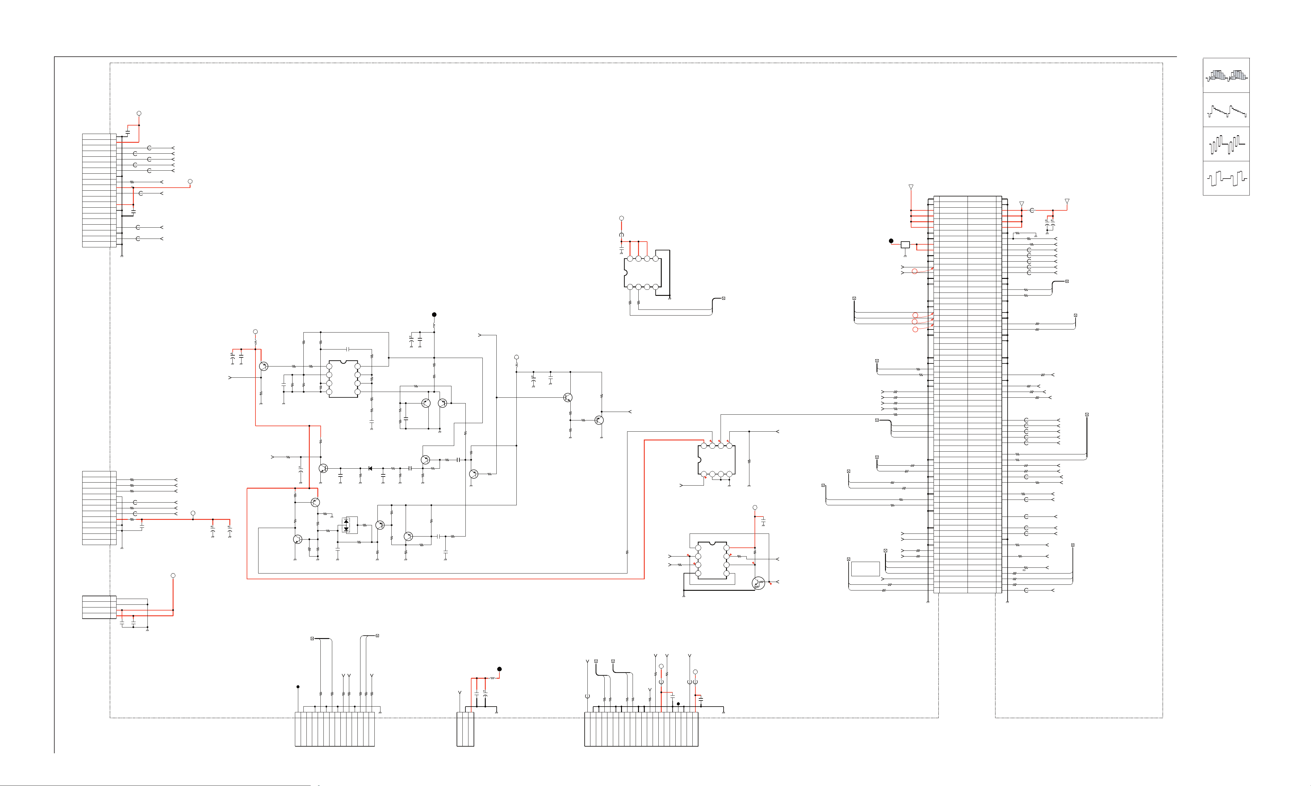
AUP BOARD SCHEMATIC DIAGRAM (3 OF 7)
KDL-70XBR3
| 62 | 52 | 42 | 32 | 22 | 12 | 02 | 91 | 81 | 71 | 61 | 51 | 41 | 31 | 21 | 11 | 01 | 9 | 8 | 7 | 6 | 5 | 4 | 3 | 2 | 1
A
—
B
—
C
—
D
—
E
—
F
—
G
—
SET_ON
11V
Q9301
2SA1576A-T106-QR
R9301
10k
1/16W
CHIP
R9302
10k
1/16W
CHIP
MA8068-TX
2SC4081T106R
F9301
3.15A
24V
D9301
Q9302
C9301
XX
R9303
1/16W
CHIP
5%
R9304
10k
1/16W
CHIP
Q9304
RSQ035P03TR
654
SDD
D3.3V
L9302
33uH
DDG
F9302
0.5A
32V
C9302
4.7
25V
X7R
3216
1k
0.5%
RN-CP
1/16W
47k
R9305
RB520S-30TE61
D9302
R9306
470k
1/16W
CHIP
5%
R9308
5.6k
1/16W
CHIP
C9303
4.7
10V
B
3216
C9306
220p
16V
CH
1005
C9304
XX
R9309
C9305
1500p
50V
B
5%
1608
3.3k
1/16W
CHIP
5%
R9311
22k
1/16W
RN-CP
0.5%
R9312
220k
1/16W
RN-CP
0.5%
R9313
47k
1/16W
RN-CP
0.5%
C9308
4.7
25V
X7R
3216
R9314
15k
1/16W
RN-CP
0.5%
R9315
10k
1/16W
RN-CP
0.5%
FB9302
0uH
1005
CH
16V
220p
C9309
321
0.5%
RN-CP
1/16W
4.7k
R9316
C9310
1
25V
2012
RSX201L-30TE25
10987654321
C9314
1000p
D9304
IC9301
BD9851EFV
SEL1
RT
CT
MON2
VREF
INV2
INV1
FB2
DTC2
PVCC2
DTC1
OUT2
PVCC1
PGND OUT1
25V
CH
1608
GND
STB
VCC
FB1
SCP
C9315
1000p
20 19 18 17 16 15 14 13 12 11
25V
CH
1608
R9323
10
1/10W
RN-CP
5%
1608
C9316
4.7
25V
X7R
3216
C9317
1
25V
2012
C9318
1
25V
2012
FB9304
D9306
1SMA5915BT
C9319
0.1
25V
1608
D3.3V
R9325
C9325
10k
150p
1/16W
50V
RN-CP
C9320
0.022
25V
1/16W
B
B
1608
RN-CP
0.5%
R9326
100k
1/16W
RN-CP
0.5%
R9327
47k
0.5%
CH
1005
R9328
3.3k
1/16W
CHIP
5%
R9329
470k
1/16W
CHIP
5%
C9326
1000p
50V
B
1608
R9335
15k
1/16W
CHIP
5%
RB520S-30TE61
D9307
C9328
4.7
10V
B
3216
SET_ON
11V
R9419
10k
1/16W
CHIP
C9408
1
25V
B
3216
R9421
0
CHIP
R9425
10k
1/16W
CHIP
PQ200WNA1ZPH
IC9403
Vin
Vc
Vo
Vadj
GND
12345
R9427
0
CHIP
Q9406
2SC4081T106R
V9V
R9429
1/16W
RN-CP
R9430
100
1/16W
RN-CP
0.5%
R9432
1k
1/16W
RN-CP
0.5%
4.7k
0.5%
R9431
1k
1/16W
RN-CP
0.5%
C9412
4.7
25V
X7R
3216
C9414
4.7
25V
X7R
3216
0
R9437
0
R9438
V9V
H
—
I
—
J
—
K
—
L
FB9301
0uH
C9307
4.7
25V
X7R
3216
4321
Q9303
RSS040P03FD5TB
8765
D9303
RSX201L-30TE25
C9311
1000p
25V
CH
1608
C9312
1000p
25V
CH
1608
L9301
10uH
R9320
10
1/10W
RN-CP
5%
1608
C9313
4.7
25V
X7R
3216
FB9303
D9305
PTZ-TE25-6.8B
R9331
0
1608
R9332
0
1608
PQ070XNA1ZPH
IC9302
Vin
Vc
12345
C9331
1
25V
2012
R9336
1k
1/16W
CHIP
5%
R9340
1/16W
RN-CP
Vo
R9338
1/16W
RN-CP
1/16W
RN-CP
1k
2.7k
0.5%
R9339
390
Vadj
C9335
4.7
25V
X7R
3216
GND
C9337
4.7
25V
X7R
3216
V5V
V5V
Q9404
DTC144EUA-T106
A9V
A9V
—
M
—
N
—
O
—
P
R9333
0
1608
R9334
0
1608
PQ070XNA1ZPH
IC9303
Vin
Vc
12345
C9332
1
25V
2012
R9337
1k
1/16W
CHIP
5%
R9343
1/16W
RN-CP
R9341
1/16W
RN-CP
1/16W
RN-CP
1k
Vo
2.7k
0.5%
R9342
390
Vadj
C9336
4.7
25V
X7R
3216
GND
C9338
4.7
25V
X7R
3216
AUP MOUNT (3/7)
POWER REGS.
D5V
D5V
A-1216-258-A<FIXP>AUP-P3
KDL-70XBR3 27
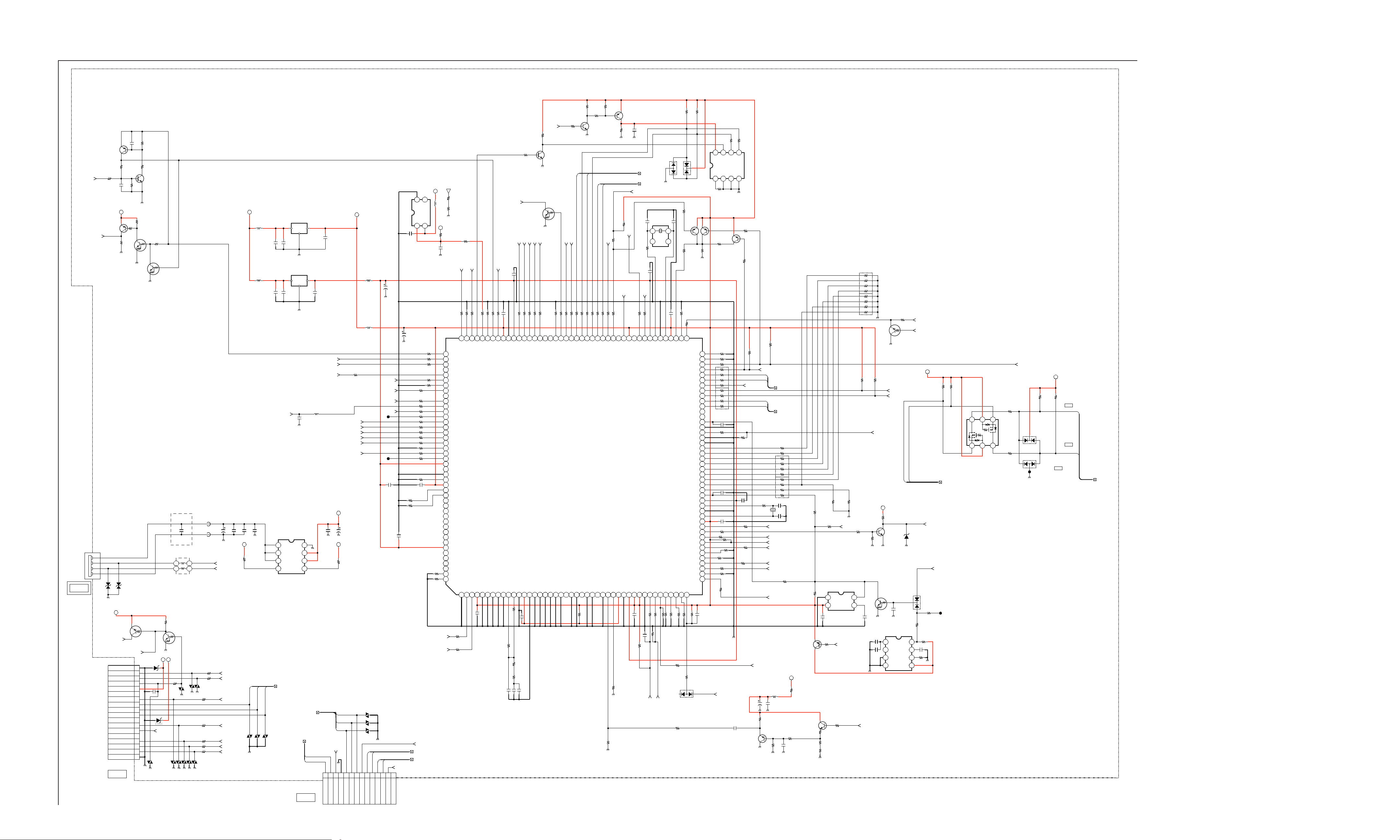
AUP BOARD SCHEMATIC DIAGRAM (4 OF 7)
A
—
C9502
0.1
10V
B
—
C
—
D
—
+B_OVP
2SA1576A-T106-QR
Q9503
2SA1576A-T106-QR
AC_RLY
Q9502
OVP
R9501
1/16W
CHIP
1k
5%
1005
R9502
10k
1/16W
CHIP
5%
C9501
0.1
10V
B
1005
STBY5V
R9505
10k
1/16W
CHIP
5%
R9503
10k
1/16W
CHIP
5%
GND_1
Q9505
DTC114EUA-T106
OVP
B
R9504
10k
1/16W
CHIP
5%
R9508
10k
1/16W
CHIP
5%
R9509
1/16W
CHIP
5%
2SC4081T106R
GND_1
R9506
10k
1/16W
CHIP
5%
GND_1
10k
Q9504
OVP
R9511
1/16W
CHIP
10k
5%
E
Q9507
DTC114EUA-T106
GND_1
OVP
—
F
—
G
—
H
—
I
—
J
—
K
—
L
—
M
—
N
—
O
—
"A" receptacle
4P
CN9501
USB
USB SMT
HORIZONTAL
C9504
1
2
3
4
D9501
D9502
PGB0010603NR
PGB0010603NR
STBY3.3V
STBY3.3V
TV_TXD
TV_RXD
TV_RST
IFP_UDP
IFP_UDM
IFP_VBUS
DEM_RST
DTT_LOG
DEM_RXD
DEM_TXD
CN9502
18P
DTA114TUA-T106
INV_MD0
1
GND
2
3
4
5
6
NC
7
8
9
10
11
NC
12
13
14
NC
15
16
17
18
GND
Q9501
MA8100-TX
MA8100-TX
VD9501
FR_MD2
TV_FLASH_W
VIN(STBY_3.3V)
DE_FLASH_W
To JIG
STBY3.3V
D9503
D9504
C9503
0.1
DTT_LOG
10k
R9507
DTC123JUA-T106
GND_1
D3.3V
R9510
VD9503
4
3
22
5%
VD9504
4
3
Q9506
L9501
VD9505
VD9506
VD9508
VD9507
0.01
25V
FB9501
1
2
1
2
VD9509
VD9510
R9513
R9514
R9515
R9516
0uH
FB9502
0uH
R9517
22
5%
R9518
22
5%
R9512
100
5%
22
5%
22
22
5%
22
5%
5%
B
12
P
KDL-70XBR3
| 32 | 22 | 12 | 02 | 91 | 81 | 71 | 61 | 51 | 41 | 31 | 21 | 11 | 01 | 9 | 8 | 7 | 6 | 5 | 4 | 3 | 2 | 1
R9583
R9589
2.2k
5%
R9585
47k
1/16W
CHIP
5%
SDA_DEVICE
CHIP
CHIP
R9587
47
47
IO_IIC_SCL3
VDDB
SCL_DEVICE
CHIP
1k
R9588
R9590
47
IO_IIC_SCL2
IO_IIC_SDA2
VSSB
BOUT
R9591
1M
1/16W
CHIP
5%
47k
1/16W
CHIP
5%
R9597
10k
1/16W
CHIP
5%
R9592
VSYNC_SEL
CHIP
5%
CHIP
1/16W
R9593
1/16W CHIP 5%
10k
I_POWER_KEY
O_MON_REC_MUTE
DATASLICERSUB
DATASLICERMAIN
R9594
1M
1/16W
CHIP
5%
Q9511
2SA1235TP-1EF
REG
R9596
C9538
10k
1/16W
CHIP
5%
POWER_SW
HDMI_INT
0
HDMI_INSEL2
R9599
3.3V
I_FE_BUS_INT
O_HDMI_SEL2
O_FE_BUS_CS/O_ANT_S
3.3V
L2.5V(1.8V)
GND
A2.5V(3.3V)
C9539
0.1
16V
X7R
1005
R9600
470
1/16W
CHIP
5%
0.5%
0.01
16V
X7R
1005
1/16W
1/16W CHIP 5%
1k
R9602
I2C_IFP
220k
CHIP
5%
C9542
16V
X7R
1005
R9601
I_HDMI_PC_INT
3.3V
C9540
I2C_DEV
0.1
0.001
50V
X7R
1005
C9541
22p
50V
CH
1005
IFP_VS
002:3F;003:7L
5%
CHIP
1/16W
1k
I_VBLK
L2.5V(1.8V)
I_KEY
GND
47
CHIP 5%
1/16W
R9603
R9604
1/16W
CHIP
KEY1
001:5B
1
32.768kHz
3
SUB_CLK_1
I_FAN_ERROR
5%
1005
47
CHIP
R9605
1/16W
10k
5%
D9507
MC2836
X9501
GND
I_AFT_MAIN
330k
R9607
R9608
1/16W
FAN_ERROR
D9508
MC2838-T112-1
C9544
15p
50V
CH
1005
2
4
1005
X7R
C9543
16V0.1
3.3V
SUB_CLK_0
I_SYNCHRO_MODE_M
I_AGC_MON
I_AFT_SUB
5%
CHIP
CHIP
1/16W
1/16W
R9610
10k
1k
CHIP
5%
R9619
4.7k
1/16W
CHIP
5%
Q9512
2SA1235TP-1EF
R9614
1/16W
CHIP
I_WAKE
I_SUB_HIN
I_PC_SYNC_DET
O_UART_TX1
I_UART_RX1
O_UART_TX0
I_UART_RX0
IO_IIC_SDA1
IO_IIC_SCL1
IO_IIC_SDA0
IO_IIC_SCL0
O_DL_MODE
O_HDMI_RST
O_HDMI_SEL
I_FE_BUS_ST
O_AGC_ATT
I_V_DET_S
I_MODEL
5%
CHIP
5%
1/16W
R9613
10k
R9618
10k
1/16W
CHIP
5%
R9615
150k
1/16W
CHIP
5%
D9509
MC2836
R9612
0
CHIP
R9623
4.7k
1/16W
CHIP
5%
R9616
10k
1/16W
CHIP
5%
R9617
47
1/16W
CHIP
5%
10k
5%
R9620
47
1/16W
CHIP
5%
8990919293949596979899100101102103104105106107108109110111112113114115116117118119120121122123124125126127128129130131132
I_CEC_IN2
I_MAIN_HIN
I_CEC_IN1
I_SIRCS
O_PC_ID
I_RESET
MD3
MD2
MD1
MD0
ICD3
ICD2
ICD1
ICD0
ICS2
ICS1
ICS0
IBREAK
ICLK
TRSTX
L2.5V(1.8V)
O_OSC
GND
I_OSC
3.3V
O_ANT_M
I_HP_DET
I_V_DET
O_BE_RST
I_BINT
5%
10kR9622
CHIP
1/16W
R9621
1k
1/16W
CHIP
5%
R9624
1/16W
CHIP
1005
10k
5%
88
87
86
85
84
83
82
81
80
79
78
77
76
75
74
73
72
71
70
69
68
67
66
65
64
63
62
61
60
59
58
57
56
55
54
53
52
51
50
49
48
47
46
45
C9545
0.001
50V
X7R
1005
R9640
47
1/16W
CHIP
5%
8765
WP
CLK
VCC
IC9506
M24128-BWMN6T(A)
EEPROM
R9626
0
CHIP
Q9513
2SA1235TP-1EF
R9627
Q9514
0
2SA1235TP-1EF
R9637
10k
1/16W
CHIP
5%
R9629
1/16W
10k
CHIP 5%
R9630
47
1/16W CHIP 5%
C9546
0.1
100516V
X7R
R9631
1/16W CHIP
10k
5%
16V0.1C9547
X7R
1005
16V
0.1C9548
1005
X7R
R9638
1/16W CHIP 5%
47
R9632
1/16W
47
CHIP 5%
R9636
10k
1/16W CHIP 5%
R9628
1/16W
10k
CHIP 5%
R9639
1/16W CHIP
22
5%
R9633
1/16W
1k
CHIP 5%
47
5%
CHIP
R9635
1/16W
B_INT
C9550
2SA1576A-T106-QR
DATA SLICER
0.1
Q9515
4321
RB9502
RB9501
0.1
X7R
R9634
R9646
DAT
47
R9642
1/16W
CHIP
C9549
R9643
R9641
47
1/16W
CHIP
5%
R9648
1/16W
CHIP
PC_ID 002:14C
47
10k
5%
16V
1005
R9645
1/16W
100
CHIP
1/16W
CHIP
1/16W
10k
1/16W
CHIP
5%
R9644
1/16W
10k
5%
5%10k
5%47
CHIP
10k
5%
R9649
10k
1/16W
CHIP
5%
HDMI_SDA
HDMI_SCL
AFT_MAIN
C9552
100
16V
BE_TXD
BE_RXD
R9651
1/16W
CHIP
0.5%
2.2k
5%
PC_SYNC_DET
X9502
10.135MHz
DL_MODE
HDMI_RST
HP_DET
HDMI_SEL
V_DET
AGC_MUTE
R9652
560
R9655
15k
R9653
1/16W
47
BE_RST
L9508
10uH
C9553
0.1
CHIP
10k
5%
1/16W
1/16W
UART_BE
I2C_HDMI
R9658
CHIP
R9659
CHIP
R9661
47
1/16W
CHIP
5%
C9557
82p
0.5%
C9555
R9660
0.5%
5%
5%47
RB9503
RB9504
18p
50V
CH
1005
C9556
18p
50V
CH
1005
D5V
4.7k
RB9505
10k
0
CHIP
RB9506
10k
R9677
R9679
10k
10k
1/16W
1/16W
CHIP
CHIP
5%
5%
FR_MD2
47
47
R9675
R9672
10k
10k
1/16W
1/16W
CHIP
R9662
CHIP
5%
R9671
0
CHIP
12
C9558
0.1
16V
X7R
1005
Q9516
R9670
10k
1/16W
CHIP
5%
Q9517
2SC4081T106R
DATA SLICER
R9668
0
1k
0.5%
R9669
1/16W
RN-CP
5%
NVM_RST
IC9507
PST3629UL
RESET
GND
VDD C
POWER_SW
R9673
33
OUT
2SC3052EF-T1-LEF
R9676
10k
1/16W
CHIP
5%
43
C9559
0.1
16V
X7R
1005
DATA_SLICER_MAIN
R9664
470
1/16W
CHIP
5%
R9665
2.2k
1/16W
CHIP
5%
2SA1576A-T106-QR
0
CHIP
R9667
0
R9678
1/16W
CHIP
Q9518
ANT-SW
10k
5%
D5V
DTC114EUA-T106
C9560
1
10V
B
1608
C9561
1
10V
B
1608
R9680
1/16W
CHIP
Q9519
RESET
4321
R9681
MAIN_H_SYNC
002:12H
INV_MD0
Q9520
DTA114TUA-T106
D3.3V
ECS_TXD
ECS_RXD
SCL_DEVICE
SDA_DEVICE
2.2k
5%
MM1096AFF
TC
NC
CK
GND VCC
C9562
0.1
10V
B
1005
RESET
IC9508
RESET
Vs
RCT
ANTSW_MAIN
D9510
MA8100-TX
D9511
M1MA152WK-T1
R9685
0
CHIP
CHIP
0
R9682
R9684
10k
1/16W
CHIP
5%
8765
C9563
4700p
50V
B
1005
R9683
0
CHIP
AUP MOUNT (4/7)
SAIPH
R9686
10k
1/16W
CHIP
5%
JIG_RST
JL9522
I2C_DEV
R9687
10k
1/16W
CHIP
5%
D1 G2 S2
SSM6N15FU(TE85R)
D2G1S1
R9688
CHIP
1005
Q9521
R9689
CHIP
1005
0
0
SIRCS
D9514
MC2838-T112-1
D9515
MC2836
JL9523
R9690
4.7k
1/16W
CHIP
D5V
R9691
4.7k
1/16W
CHIP
5%
5%
DAT
SDA_DEV_5V
CLK
SCL_DEV_5V
GND
I2C_DEV_5V
A-1216-258-A<FIXP>AUP-P4
1/16W
CHIP
Q9510
2SC3052EF-T1-LEF
NVM_RST
R9574
47k
1/16W
CHIP
5%
Q9508
2SC3052EF-T1-LEF
NVMWP
R9569
10k
1/16W
CHIP
5%
VOLTAGEDETECTOR
IC9504
S-80828CNNB-B8NT2G
STBY5V
3.3V REG
MM3123DPLE
L9502
10uH
C9511
1
16V
B
2012
L9503
10uH
C9512
1
16V
B
2012
TV_FAN_DRV
12
1
C9505
100
16V
12
2
USB_UDM
USB_UDP
ECS_TXD
ECS_RXD
002:11B
JIG_RST
DE_RST
DE_FLASH_W
DE_UART_RX_JG
DE_UART_TX_JG
C9506
10
10V
B
3216
002:11B
C9507
10
10V
B
3216
R9519
100k
1/16W
CHIP
12
5%
IFP_UDP
VD9511
12
VD9512
C9508
0.1
25V
B
IFP_UDM
IFP_USB
IFP_VBUS
VD9513
IC9501
I
VSS
C9513
0.1
16V
X7R
1005
1.8V REG
MM3121JPLE
IC9502
I
VSS
C9514
0.1
16V
X7R
1005
POWER DST.SW
IC9503
TPS2051ADR
8
8765
GND
OUT
7
6
5
IN
OUT
IN
OUT
EN
/OC
O
O
C9515
0.01
16V
B
1005
4321
I2C_DEV
1
2
3
4
PNL_USB
C9518
0.1
10V
B
1005
C9517
0.1
10V
B
1005
SET_ON
002:11B
VSW_PW_CTRL
PFC_DET
L9504
10uH
12
C9520
0.1
25V
B
1608
SDA_DEVICE
SCL_DEVICE
123456789
CLK_REC3
DAT_REC3
STBY1.8V
D5V
1
2
D3.3VD3.3V
PNL_VBUS
B_INT
B_INT
STBY3.3V
HDMI/DTT_SW
C9522
100
16V
R9523
10k
1/16W
CHIP
12
5%
PNL_UDM
PNL_UDP
GND
PNL_UDP
STBY3.3V
R9524
1k
1/16W
CHIP
5%
HP_MUTE
LINE_MUTE
SP_MUTE
SP_PROT
DLY_RST
PNL_UDM
PNL_VBUS
L9505
10uH
L9506
10uH
VD9514
VD9515
VD9516
DIC_SCL
CLK_W3
WEM_LOG
DIC_SDA
C9523
10V
AMP_RST
LOGO
AP_RST
DLY_MUTE
JL9514
JL9515
C9524
0.1
16V
X7R
1005
IFP_SCL
IFP_SDA
1011121314
DAT_W3
CLK_IFP3
BE_BOOT
DAT_IFP3
C9527
0.1
16V
X7R
1005
22
C9526
22
10V
R9528
47
R9542
47
R9543
47
R9529
R9530
R9544
47
R9545
47
R9531
R9546
1k
R9532
R9533
10k
R9534
10k
R9535
R9536
10k
R9526
10k
CHIP
1/16W
1005
5%
R9527
10k
CHIP
1/16W
1005
5%
C9525
0.1
16V
X7R
1005
BE_BOOT
NC
14P
CN9503
43
GND
OUT
12
R9538
47
R9539
47
R9540
47
R9541
10k
1/16W CHIP
47
1/16W
47
1/16W
47
1/16W
47
1/16W
1/16W CHIP 5%
1/16W CHIP 5%
47
1/16W
1/16W CHIP
C9528
0.1
16V
X7R
1005
WEM_LOG
I2C_DIC
I2C_IFP
D5V
VCC NC
R9537
47
1/16W
CHIP
5%
1/16W
CHIP 5%
1/16W CHIP 5%
1/16W
CHIP 5%
1/16W
CHIP 5%
5%
CHIP 5%
CHIP 5%
CHIP 5%
CHIP 5%
CHIP 5%
5%
R9549
1/16W
R9547
1/16W
CHIP
CHIP
47
5%
47
5%
L9507
1uH
D3.3V
CCDM_H
CCDS_H
11V
R9550
22k
1/16W
CHIP
5%
R9551
10k
1/16W
CHIP
5%
R9548
470
1/16W
CHIP
5%
R9555
C9529
0.01
16V
X7R
1005
133
134
135
136
137
138
139
140
141
142
143
144
145
146
147
148
149
150
151
152
153
154
155
156
157
158
159
160
161
162
163
164
165
166
167
168
169
170
171
172
173
174
175
176
0
CHIP
002:3K
002:3J
HDMI_CE
WRT_PRT
5%
5%
5%
5%
5%
CHIP
CHIP
1/16W
1/16W
1/16W CHIP
R9556
R9557
R9558
1k
1k
1k
I_SP_DET
O_AC_RLY
O_HDMI_CE
O_BE_ON
O_VSW_PW_CTRL
O_FE_ON
I_AC_DET
O_AMP_RST
I_MIPS_RST
O_LOGO_LED
O_CEC_OUT
O_AP_RST
O_FAN_DRV
O_DLY_MUTE
O_DIR_MUTE
O_HP_MUTE
O_LOUT_MUTE
O_SP_MUTE
I_SP_PROT
O_HDMI_DTT_SW
I_DIR_ERR
O_DLY_RST
O_DIR_RST
L2.5V(1.8V)
USB_CLK_1
GND
USB_CLK_0
3.3V
UDM
UDP
D_B0
D_B1
D_B2
D_G0
D_G1
D_G2
D_R0
D_R1
D_R2
L2.5V(1.8V)
YM_OUT
YS_OUT
FH
DOT_CLK_O
DOT_CLK_I
OSD_V
MAIN_H
OSD_H
1234567891011121314151617181920212223242526272829303132333435363738394041424344
R9552
47
1/16W
CHIP
5%
R9553
47
1/16W
CHIP
5%
CHIP
R9559
1/16W
1k
O_NVM_WP
O_PC_HDMI_WP
3.3V
SUB_H
C9530
0.1
16V
X7R
1005
1/16W CHIP 5%
R9560
1k
I_LB_ERR
GND
CHIP
R9561
1/16W
1k
I_D_OVP
VGS1
R9562
1/16W CHIP5%10k
I_PB_OVP
CPO1
002:3G
BE_WDT
C9531
0.1
16V
X7R
1005
I_BE_WDT
VSSP1
C9534
3.3V
VDDP1
C9533
1005
100p
50V
1005
FE_RST
PMUTE_LED
ON_TIMER_LED
0.1
16V
X7R
5%
5%
CHIP
CHIP
CHIP
R9568
R9570
R9571
1/16W
1/16W
1k
1k
GND
L2.5V(1.8V)
O_TIMER_LED
O_PMUTE_LED
VDDP2
VSSP2
CPO2
VGS2
CHIP
5%
3.3k
R9565
1/16W
C9537
0.1
16V
1005
0
1005
CHIP
R9564
R9566
180
1/16W
RN-CP
0.5%
0.5%
R9567
330
1/16W
RN-CP
0.5%
0.5%
C9536
0.22
6.3V
B
B
1005
C9535
0.1
10V
B
1005
REC_LED
5%
5%
CHIP
R9572
1/16W
1/16W
1k
1k
O_LAMP_LED
VGS3
STBY_LED
POWER_LED
5%
CHIP
R9573
1/16W
1k
O_PWR_LED
O_STBY_LED
VSSP3
CPO3
DTC114EUA-T106
O_SPI_SO3
O_SPI_SCK3
VDDR
VDDP3
RESET
R9578
10k
1/16W
CHIP
5%
IFP_SDA
Q9509
RESET
002:3I
002:3I
TXD_ATSC
RXD_ATSC
1/16W
R9580
R9579
R9577
R9576
47
0
1/16W CHIP 5%100
0
1/16W CHIP 5%10k
R9575
I_SPI_SI3
O_FE_RST
I_UART_RX2
O_UART_TX2
IC9505
MB91F318RPMC-G001-9035E1
SAIPH
VSSR
ROUT
VRO
VREF
IFP_SCL
5%
CHIP
R9584
R9582
1/16W
47
IO_IIC_SDA3
IO_IIC_SDA4
GOUT
VDDG
R9581
0
CHIP
1/16W
R9586
47
IO_IIC_SCL4
VSSG
To JIG
KDL-70XBR3 28
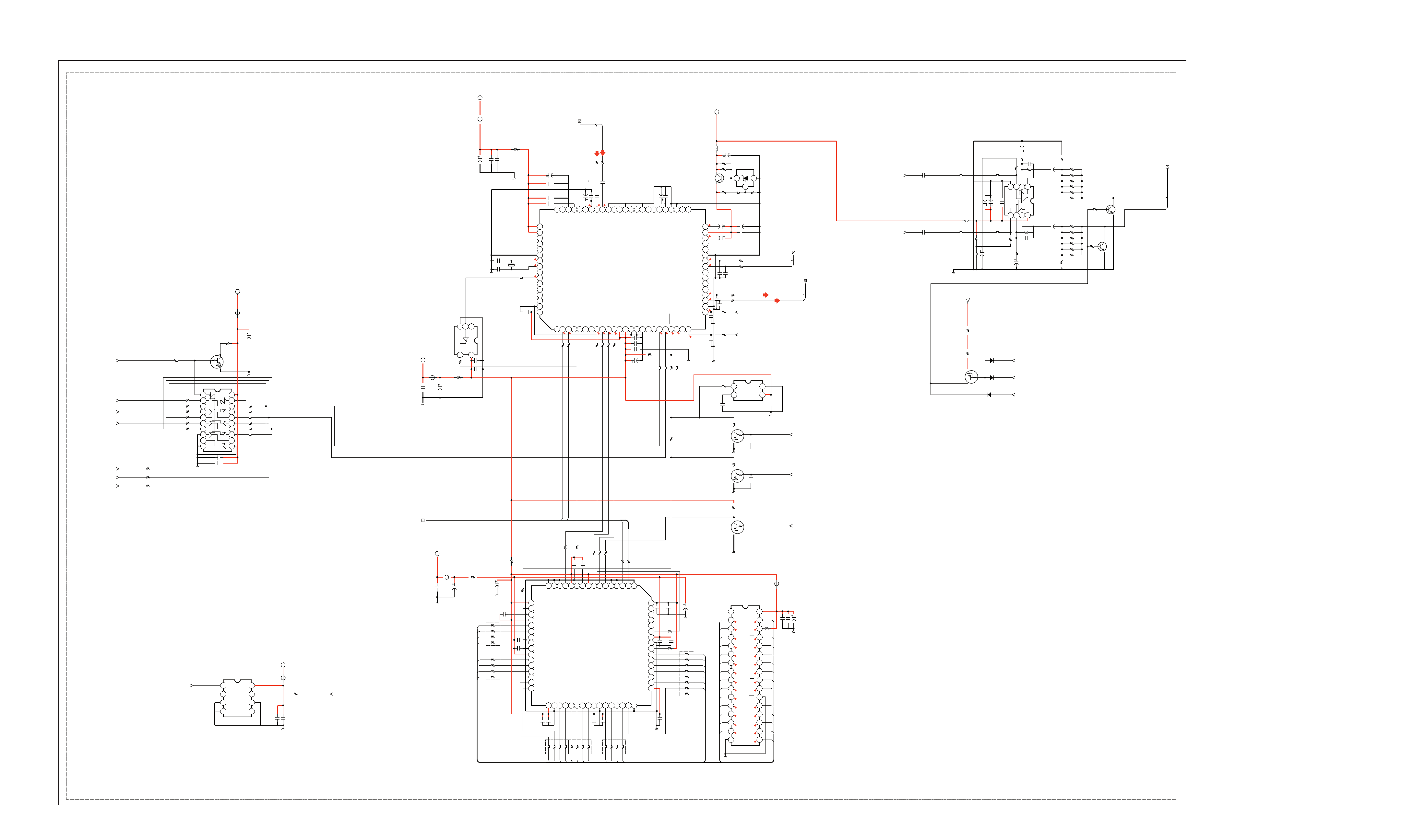
AUP BOARD SCHEMATIC DIAGRAM (5 OF 7)
A
KDL-70XBR3
| 42 | 32 | 22 | 12 | 02 | 91 | 81 | 71 | 61 | 51 | 41 | 31 | 21 | 11 | 01 | 9 | 8 | 7 | 6 | 5 | 4 | 3 | 2 | 1
D5V
—
B
—
C
—
D
—
E
—
F
—
G
—
H
—
I
—
HDMI/DTT_SW
DTT_BCK
DTT_LRCK
DTT_DA1
HDMI_BCK
HDMI_LRCK
HDMI_DA1
R8402
R8403
R8404
0
0
0
R8407
1/16W47
IC8401
SN74AHCT244PWR
OCTALBUS DRIVER
A9V
0uH
FB8406
R8461
0
1608
C8439
C8433
C8431
47
16V
D5V
0uH
FB8402
C8426
16V
321
NC
GND
IN A
OUTY
VCC
R8459
1608
54
0
R8554
47
1/16W
CHIP 5%
10
R8427
10k
1/16W
CHIP
5%
Q8401
MUN2211T1
SW
12345678910
1/16W47R8412
1/16W47R8413
1/16W47R8414
1/16W47R8415
1/16W47R8416
1/16W47R8417
Vcc
GND
C8411
10V0.1
1005
B
C8413
10
16V
20 19 18 17 16 15 14 13 12 11
1/16W47R8430
1/16W47R8431
1/16W47R8432
1/16W47R8433
1/16W47R8434
1/16W47R8435
C8410
1000p
50V
CH
1005
IC8404
TC7SZU04FU(TE85R)
INVERTER
D5V
FB8404
0uH
C8423
100p
50V
CH
1005
0.1
10V
B
1005
C8430
1000pCH
C8432
0.1
10V
B
1005
100550V
100p
50V
CH
1005
C8437
50V
X8402
18.432MHz
C8438
4p
1005
CH
100550V4pCH
R8466
1/16W CHIP
5%47
C8443
1000p
50V
1005
C8447
47
16V
C8448
16V0.22
C8450
100p
50V
C8449
AVSUP
65
AVSUP
66
IF_IN1
67
IF_COMMON_IN
68
IF_IN2
69
TEST
70
2.0
XTAL_IN
71
2.1
XTAL_OUT
72
TP
73
2.6
AUDIO_CLOCK_OUT
74
NC
75
SPDIF_OUT
76
DIGITAL_CONTROL_OUT_1
77
DIGITAL_CONTROL_OUT_0
78
ADR_SEL
79
STANDBYQ
80
CH
MAIN_INV_LR
MAIN_INV_LR_L
MAIN_INV_LR_R
R8479
R8476
100
100
1/16W
1/16W
22C8460
C8457
NC
IF_GND
I2C_CL
I2C_DA
4.3
5%100
R8471
1/16W CHIP
SDA_DEV_5V
4.4
R8473
5%100
1/16W CHIP
IF_GND
I2S_CL
C8456
10
16V
2.6
SC5_IN_R
I2S_WS
0.22
B
16V
1608
SC5_IN_L
REF_VOLTAGE
I2S_DA_OUT
I2S_DA_IN1
16V
22
16V
3.7
3.6
C8459
ASGND1
SC1_IN_L
SC1_IN_R
MAP4400A-QA-B2-501-T
I2S_DEL_IN
I2S_DEL_OUT
I2S_DEL_CL
0.7
0.9
2.5
5%47
5%47
5%47
R8477
R8483
R8480
1/16W CHIP
1/16W CHIP
1/16W CHIP
SC2_IN_L
SC2_IN_R
IC8405
AUDIODSP
I2S_DEL_WS
DVSUP
2.5
5%47
R8486
1/16W CHIP
ASGND2
DVSUP
C8467
0.22 B
SC3_IN_R
D_GND
16V
1608
C8466
47
16V
SC3_IN_L
D_GND
C8471
10
16V
ASGND4
SC4_IN_R
D_GND
I2S_DA_IN2NCI2S_CL3
C8465
1000p
50V
1005
CH
C8464
50V100p
1005
CH
R8492
1/16W47k
SC4_IN_L
NC
R8494
2.5
5%47
1/16W CHIP
C8472
0.1
10V
B
1005
A_GND
REF_VOLTAGE
I2S_WS3
RESETQ
2.5
4.1
5%47
CHIP0
R8498
R8495
1/16W CHIP
SUBWOOFER_OUT
B
1608
CH
1005
CH
100550V1000p
NC
NC
123456 7 8910 11 12 13 14 15 16 17 18 19 20 21 22 23 24
SCL_DEV_5V
A_GND
SC3_OUT_L
SC1_OUT_L
SC1_OUT_R
VREFGND1
SC2_OUT_L
SC2_OUT_R
VREFGND2
I2S_DA_IN3
I2S_DA_IN4
0.0
5%47
CHIP
R8499
1/16W
R8447
CHIP0
414243444546474849505152535455565758596061626364
CAPL_M
SC3_OUT_R
AHVSUP
CAPL_A
SUR_L
SUR_R
SP_OUT_C
SP_OUT_L
SP_OUT_R
DACA_L
DACA_R
0.1
R8559
220
1/10W
RN-CP
0.5%
C8479
1000p
50V
1005
R8504
1/10W
RN-CP
0.5%
40
39
38
37
36
35
34
33
32
31
30
29
28
27
26
25
B
220
L8403
10uH
3.8
0.1
0.1
0.1
6.7
6.8
C8486
3.8
C8478
1000p
C8483
47
16V
Q8405
2SC4081T106R
REG
R8560
270
1/10W
RN-CP
0.5%
C8485
10
16V
10
16V
C8490
330p
1005
C8487
CH
330p
1005
C8481
CH
330p
1005
CHC8482
1005
330p
R8505
0
CHIP
50V
B
1005
R8506
0
CHIP
R8502
0
CHIP
1005
C8510
0.033
10V
B
1005
IC8408
TL431CPK-E2
3
R8511
10k
1/10W
RN-CP
0.5%
C8491
47
16V
C8492
CH
0
0
CH
R8509
CHIP
0
R8510
CHIP
0
HP_L_AMP
HP_R_AMP
43
OUT
IC8410
PST3641UL
CD
RESET
R8448
100
1/16W
CHIP
5%
1005
Q8406
MUN2213T1
R8446
100
1/16W
Q8413
MUN2213T1
1
1000p
R8512
R8513
100550V
CHIP
CHIP
R8514
1/10W
RN-CP
0.5%
4.7k
2
GND
VDD
C8489
C8477
16V
1608
16V
1608
0.1
B
0.1
B
SCART2_LR_OUT_L
SCART2_LR_OUT_R
L
12
C8511
0.01
16V
1005
C8505
4.7
35V
R8530
4.7k
1/16W
C8507
+
R8529
4.7k
1/16W
C8504
35V
+
4.7
47p
R8532
47k
1/16W
NJM3414AV(TE2)
8765
R8531
47k
1/16W
C8506
47p
IC8409
OP-AMP
C8502
100
16V
R8525
1/16W
C8503
0.1
16V
1005
R8526
1/16W
R8528
47k
1/16W
1k
4321
R8527
1k
47k
1/16W
C8496
2.2
B
10V
HP_R_AMP
HP_L_AMP
SCART2
SP
SP_LR_OUT_L
SP_LR_OUT_R
R
2012
C8497
10V
2012
R8562
0
CHIP
C8512
100
16V
L8404
10uH
R8561
R8523
2.2
B
CHIP
0
10k
1/16W
C8501
11V
R8524
1/16W
10
10k
16V
C8508
47
16V
C8509
47
16V
R8534
10k
1/10W
RN-CP
5%
R8533
10k
1/10W
RN-CP
5%
470R8535
1/10W RN-CP
1kR8536
1/10W
RN-CP
1kR8537
5%
1/10W
RN-CP
470R8538
1/10W RN-CP
1kR8539
1/10W
RN-CP
1kR8540
5%
1/10W
RN-CP
470R8541
1/10W RN-CP
1kR8542
1/10W
RN-CP
1kR8543
5%
1/10W
RN-CP
470R8544
1/10W RN-CP
1kR8545
1/10W
RN-CP
1kR8546
5%
1/10W
RN-CP
Q8412
2SC3624A-T1L15L16
MUTE
R8548
3.3k
1/16W
CHIP
5%
R8547
3.3k
1/16W
CHIP
5%
Q8411
2SC3624A-T1L15L16
MUTE
HP_LR_OUT
HP_R
HP_L
HEADPHONE OUT
R8520
0
CHIP
R8521
0
CHIP
D8411
MA111-TX
D8413
Q8410
MUN2111T1
MUTE
B
AP_RST
DLY_RST
MA111-TX
MA111-TX
D8414
INV_AC_MUTE
INV_HP_MUTE
ON/OFF_MUTE
J
—
K
—
L
—
M
—
N
—
O
—
EMMA_SPDIF
TRIPLENON-INVERTER
TC7WZ34FK(TE85R)
IC8402
4321
D3.3V
8765
C8417
50V1000p
1005
CH
C8418
1005
R8501
47k
1/16W
CHIP
5%
I2C_DEV_5V
5%
5%
R8474
R8472
1/16W
1/16W
47
A14
C8453
100p
50V
CH
1005
IIS2_IN
GND
A12
IIS1_IN
A12
A7
IISM_IN
A7
A6A8A5
47
XSM
A6
GND
FCLK
AUDIODELAY
CXD9826R
A4
A5
A4
D3.3V
R8462
0
1608
0uH
FB8405
C8425
100p
50V
CH
1005
0uH
FB8401
R8444
1/16W CHIP
100
0.1
10V
B
OPTOUT
5%
C8429
10
16V
R8460
1608
0
16V
47
C8440
100
RB8401
A15
WE
A13
100
RB8402
A9
A11
OE
A10
C8441
10V
1005
0.1
B
C8445
1005
C8444
1000p
50V
0.1
10V
1005
R8469
CHIP0
IIS3_IN
17
XTST
18
RST
19
GND
20
OVDDH
21
A15
22
FWR
23
C8451
A13
24
A8
25
GND
26
VDDL
27
A9
28
A11
29
FRD
30
A10
31
A16
32
A14
0.1
100510V
B
C8446
1000p
50V
1005
100
RB8403
A16
OVDD
3334353637383940
CH
B
CH
5%
5%
5%
R8478
R8475
1/16W
R8481
1/16W
1/16W
47
47
BIT_CLK
47
LR_CLK
MUTE (H=Mute)
C8455
0.01
16V
1005
B
VDDH
IC8406
A2
A3
GND
VDDH
4142434445464748
C8461
C8458
0.1
1000p
50V
10V
CH
B
1005
1005
100
100
RB8405
RB8404
A2
A3
A1
S_ADD0
A1
A0
SDA_DEV_5V
SDA
S_ADD1
IO7
A0
IO7
R8488
5%
1/16W
100
SCL_DEV_5V
5%
R8490
1/16W
100
123456789 10111213141516
GND
SCL
BIT_CLK_OUT
IIS3_OUT
IIS2_OUT
IIS1_OUT
IISM_OUT
IO6
GND
OVDDH
VDDL
GND
F_SW
IO0
IO1
IO2
IO3
IO4
IO5
OVDDH
Q8404
MUN2213T1
C8473
0.1
10V
B
1005
64
C8468
100p
50V
63
CH
1005
62
61
60
59
C8469
58
1000p
50V
57
1005
CH
56
R8497
1/16W
CHIP 5%
55
54
53
52
51
50
49
C8470
0.01
16V
B
1005
C8476
10
16V
R8496
1/16W CHIP
RB8407
100
RB8406
100
5%47
IO0
IO1
IO2
IO3
IO4
IO5
IO6
C8474
0.1
10V
B
1005
10k
SRAM
M5M51008DFP-70H
IC8407
123456
NC
A16
A16
3.9 2.7
A14
A14
2.5 4.9
A12
A12
2.4 4.5
A7
A7
2.5 2.4
A6
A6
2.5 2.5
789
A5
A5
2.5 2.6
A4
2.5 2.6
A3
A3
2.5 4.5
10 11 12
A2
A2
2.4
A1
A1
2.5
A0
A0
2.5 1.8
13 14 15 16
I/O1
2.2 1.8
IO1
I/O2
2.3 1.9
IO2
I/O3
2.0 1.9
VSS I/ O 4
32 31 30 29 28 27
VCC
A15
CS2
WE
A13
A8
26 25 24
A9
A11
OE
23 22 21 20
A10
2.5
CS1
I/O8
IO7
19 18 17
I/O6
I/O5
1.8
A15
R8515
1/16W
WE
CHIP
A13
A8
A9
A11A4
OE
A10
IO7
IO6IO0
IO5
IO4
IO3
DLY_MUTE
FB8408
0uH
C8493
1000p
50V
CH
1005
C8495
10
16V
C8494
1k
0.1
10V
B
5%
1005
AUP MOUNT (5/7)
AUDIODSP
P
A-1216-258-A<FIXP>AUP-P5
KDL-70XBR3 29
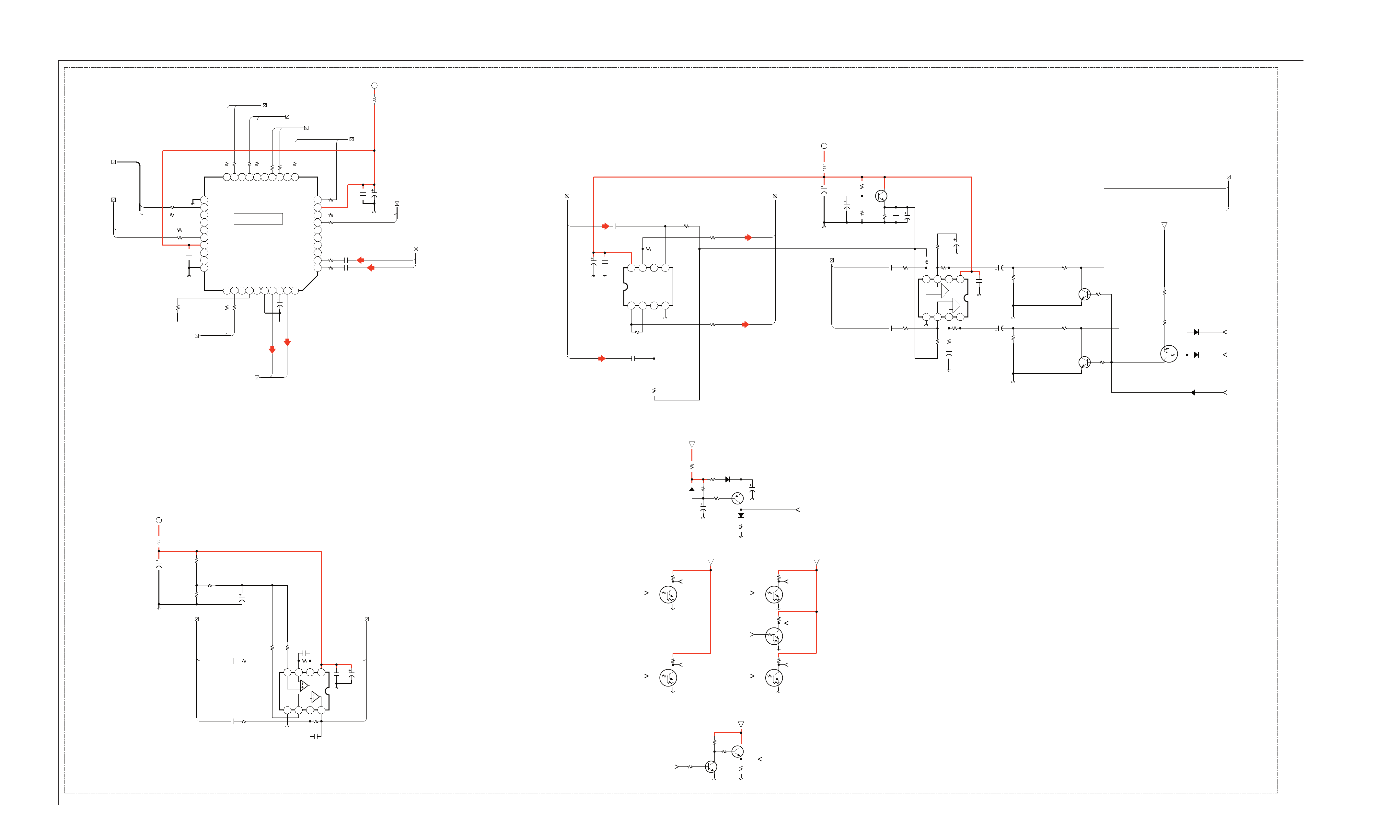
AUP BOARD SCHEMATIC DIAGRAM (6 OF 7)
KDL-70XBR3
| 62 | 52 | 42 | 32 | 22 | 12 | 02 | 91 | 81 | 71 | 61 | 51 | 41 | 31 | 21 | 11 | 01 | 9 | 8 | 7 | 6 | 5 | 4 | 3 | 2 | 1 72
A
—
B
—
C
—
D
—
E
—
F
—
G
—
COMP3_LR_IN
HDMI_LR_IN
HDMI_LR_IN_L
HDMI_LR_IN_R
COMP3_L
COMP3_R
R8732
4.7k
1/16W
CHIP
R8733
4.7k
1/16W
CHIP
R8621
0
CHIP
R8615
4.7k
R8616
4.7k
5%
5%
C8604
0.1
16V
1005
I2C_DEV_5V
1/16W
1/16W
A9V
L8603
C8623
0.1
16V
1005
10uH
C8625
100
16V
PC_AU_R
PC_AU_L
PC_LR_IN
TV_M_AMP_R
TV_M_AMP_L
TV_M_AMP_LR_IN
TV_M_LR_IN
TV_M_L_IN
TV_M_R_IN
16V
22
C8663
C8661
10
16V
0.1
C8664
B
25V
1608
8765
NJM4558V-TE2
OPAMP
R8748
0
CHIP
C8662
10
16V
R8753
0
CHIP
IC8605
47k
R8757
4321
CHIP
1/16W
A9V
L8601
10uH
R8601
TV_M_AMP_LR_IN
R8756
47k
1/16W
5%
R8755
0
R8750
0
CHIP
TV_M_AMP_L
TV_M_AMP_R
C8601
100
16V
SCART2
6.8k
1/16W
C8602
10
16V
R8602
12k
1/16W
SCART2_LR_OUT_L
SCART2_LR_OUT_R
Q8601
2SC4081T106R
R8605
1k
C8609
1/16W
0.1
10V
B
1005
C8607
10
16V
IC8601
NJM4558V-TE2
OPAMP
C8608
10
16V
C8610
100
16V
R8606
0
CHIP
R8607
0
CHIP
R8611
2.2k
RN-CP
R8609
47k
1/16W
R8612
1k
1/16W
RN-CP
0.5%
+
4321
R8613
47k
1/16W
+
-
R8618
2.2k
1/16W
RN-CP
C8613
10
16V
C8612
10
16V
8765
R8617
1/16W
RN-CP
0.5%
11V
C8615
0.1
16V
1005
C8618
10
16V
1k
C8619
10
16V
R8626
47k
1/16W
R8627
47k
1/16W
R8634
560
1/16W
Q8606
2SC3624A-T1L15L16
MUTE
R8635
560
1/16W
Q8607
2SC3624A-T1L15L16
MUTE
R8643
3.3k
1/16W
R8652
1/16W
3.3k
11V
R8655
0
CHIP
R8656
0
CHIP
Q8611
MUN2111T1
MUTE
D8603
MA111-TX
D8605
MA111-TX
MA111-TX
D8606
LINE_LR_OUT
LINE_L
LINE_R
INV_AC_MUTE
INV_LOUT_MUTE
ON/OFF_MUTE
COMP1_LR_IN
5%
14
IN5_R
ROUT1
V1_L
R8633
1/16W
13
IN5_L
BIAS
4.7k
V3_LR_IN
5%
12
NC
LOUT1
C8622
100
16V
R8638
SIDE_LR_IN_R
4.7k
5%
1/16W
11
IN4_R
IN4_L
AVCC
IN3_R
IN3_L
NC
IN2_R
IN2_L
NC
IN1_R
IN1_L
NC
40
MAIN L
V1_LR_IN
5%
12345678910
R8646
4.7k
R8647
4.7k
R8650
4.7k
R8651
4.7k
1/16W
SIDE_LR_IN_L
R8645
4.7k
1/16W
1/16W
5%
1/16W
5%
5%
1/16W
5%
5%
SIDE_LR_IN
C8659
22
16V
C8660
22
16V
COMP1_L
COMP1_R
R8624
4.7k
1/16W
R8622
4.7k
1/16W
19
20
21222324252627282930
IN7_R
AGND
IN8_L
IN8_R
NC
IN9_L
IN9_R
LVCC
IN10_L
IN10_R
LGND
CLK-1
313233343536373839
R8623
47
1/16W
SCL_DEV_5V
SDA_DEV_5V
V3_L
V3_R
V1_R
R8629
4.7k
1/16W
R8628
1/16W
IN7_L
4.7k
R8632
5%
18
NC
5%
17
IN6_R
16
IN6_L
4.7k
1/16W
15
5%
NC
AUDIO SW
IC8603
CXA2188Q-T4
DAT-1
ROUT2
ADR
LOUT2
MUTE
R8625
5%
5%
47
1/16W
MAINR
MAIN_LR_OUT
H
—
I
—
J
—
K
—
L
—
M
—
N
A9V
L8604
10uH
C8627
100
16V
R8664
8.2k
1/16W
R8665
10k
1/16W
MAIN_LR_OUT
AUDIO SWITCH
R8746
0
C8636
100
16V
C8639
220p
50V
B
1005
MAIN_LR_OUT_L
C8633
22
16V
R8670
4.7k
1/16W
R8673
47k
1/16W
R8679
47k
1/16W
R8682
3.3k
1/16W
8765
MAIN_INV_LR
MAIN_INV_LR_L
C8642
0.1
16V
C8617
1005
100
16V
AC_MUTE
HP_MUTE
R8717
10k
Q8628
MUN2211T1
MUTE
R8719
Q8630
MUN2211T1
MUTE
10k
11V
R8720
0
CHIP
INV_AC_MUTE
INV_HP_MUTE
R8722
1/16W
CHIP
D8615
MA111-TX
C8657
R8725
1/16W
CHIP
47k
10
16V
11V
470
LINE OUT
D8616
MA111-TX
C8658
MA111-TX
R8727
1M
5%
1/16W
CHIP
LINE_MUTE
SP_MUTE
AMP_RST
100
16V
D8617
MUN2211T1
Q8632
2SA1576A-T106-QR
R8729
10k
Q8634
MUN2211T1
MUTE
R8730
10k
Q8635
MUN2211T1
MUTE
R8731
10k
Q8636
RESET
ON/OFF_MUTE
11V
INV_LOUT_MUTE
INV_SP_MUTE
INV_AMP_RST
5%
5%
R8723
22k
1/16W
CHIP
5%
—
O
—
P
MAIN_LR_OUT_R
C8634
16V
R8671
22
4.7k
1/16W
4321
R8683
3.3k
1/16W
C8640
220p
50V
B
1005
MAIN INV AMP
IC8604
NJM4558V-TE2
MAIN_INV_LR_R
PFC_DET
R8724
100k
1/16W
R8721
100k
1/16W
Q8631
2SC4081T106R
PFC-DET
R8726
100
1/16W
11V
Q8633
2SC4081T106R
MUTE
R8728
1k
1/16W
MUTE
AC_MUTE
AUP MOUNT (6/7)
AUDIO SWITCH
A-1216-258-A<FIXP>AUP-P6
KDL-70XBR3 30
 Loading...