

Page 1

HISTORY
When clicking an item, it’s detail is displayed.
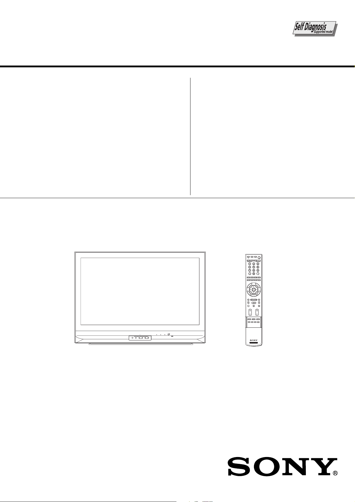
Model Name: KDF-E42A10/E50A10
SERVICE MANUAL
Part No. : 9-872-749-04
Date SUPP./CORR. Description of SUP/COR
2005.6 – NEW –
2005.8 CORR.-1 Addition of LAMP XL-2400 (Page 72) Yes
2005.10 CORR.-2 Deleted of LAMP BLOCK ASSY (Page 62) Yes
2005.12 SUPP.-1 Addition of SERVICE MANUAL FOR BOARD REPAIR Yes
CENTER (APPENDIX)
Change of
main text
Page 2
SERVICE MANUAL
MIX5
CHASSIS
MODEL COMMANDER DEST. CHASSIS NO.
–––––– –––––––––––– ––––– –––––––––––
KDF-E42A10
KDF-E42A10
KDF-E42A10
KDF-E50A10
KDF-E50A10
KDF-E50A10
RM-YD003
RM-YD003
RM-YD003
RM-YD003
RM-YD003
RM-YD003
USA
CANADA
MEXICO
USA
CANADA
MEXICO
MODEL COMMANDER DEST. CHASSIS NO.
–––––– –––––––––––– ––––– –––––––––––
TIMER LAMP
PUSH OPEN
WEGA GATE
TV/VIDEO
CANNELVOLUME
KDF-E42A10/E50A10
POWER/STANDBY
TV/VIDEO
POWER TV POWER
MUTING
DVD/
SAT/
VCR
CABLE
DVR
TV
FUNCTION
ENT
JUMP ANT MTS/SAP FREEZE
SOUND PICTURE
TV/SAT
WIDE
SUR
D
IS
E
P
ID
L
A
U
Y
G
R
E
T
LS
U
R
OO
T
N
W
E
E
T
G
A
A
G
REPLAY ADVANCE NEXTPREV
PLAY
VISUAL SEARCH
PAUSE
STOP
CH
VOL
REC REC PAUSE REC STOP
TOP MENU MENU F1 F2
POWER
RM-YD003
LCD PROJECTION TV
Page 3
KDF-E42A10/E50A10
K RM-YD003 RM-YD003
Specifications
Projection System 3 LCD Panels, 1 lens projection system
LCD Panel 0.73 inch TFT LCD panel (1,280
Projection Lens High Performance, large diameter hybrid lens F2.4
Antenna 75-ohm external terminal for VHF/UHF
Lamp 100W, XL-2400
Telev is io n System NTSC American TV Standard
ATSC ( 8VSB terrestrial) ATSC compliant 8VSB
QAM on cable ANSI/SCTE 07 2000
Visible Screen Size (Picture measured
diagonally)
KDF-E42A10: 42 inches
KDF-E50A10: 50 inches
Channel Coverage Terrestrial (analog) 2-69
Cable TV (analog) 1-125
Terrestrial (digital) 2-69
Cable TV (digital) 1-135
Number of Inputs/Outputs
HDMI IN Video 1080i, 720p, 480p, 480i
Audio Two channel linear PCM 32, 44.1 and 48 kHz,
Vid eo (I N) 3 total (1 on side panel) 1 Vp-p, 75 ohms unbalanced, sync negative
S Video (IN) 1 Y: 1 Vp-p, 75 ohms unbalanced, sync
Audio (IN) 5 total (1 on side panel) 500 mVrms (100% modulation)
Component Video Input 2 (Y P
B/CB PR/CR
) Y: 1 Vp-p, 75 ohms unbalanced, sync
AUDIO (VAR/FIX) OUT 1 500 mVrms at the maximum volume setting
RF Inputs 2
PC Input 1
Digital Audio Optical Output
(PCM/Dolby
Digital)
1Optical Rectangular (1)
CableCARD Slot PCMCIA Type I/II
Speaker output 12 W + 12 W
Power requirement120 V, 60 Hz
Power consumption In use: 210 W
In standby: Le
ss than 17 W
⋅
720 pixels)
16, 20 and 24 bit
negative
C: 0.286 Vp-p (Burst signal), 75 ohms
Im
pedance: 47 kilohms
negative
B/CB
: 0.7 Vp-p, 75 ohms
P
P
R/CR
: 0.7 Vp-p, 75 ohms
(Variable)
500 mVrms (Fixed)
Impedance (output): 2 kilohms
AUDIO
OUT jacks are operable only w hen th e
TV
’s Spe aker is set to O ff .
– 2 –
Page 4
KDF-E42A10/E50A10
K RM-YD003 RM-YD003
Dimensions (W/H/D)
Mass KDF-E42A10: 28 kg (61 lb. 12 oz.)
Supplied Accessories
Remote Control RM-YD003
AA (R6) Batteries 2 supplied for remote control
Operati ng Instructions 1
Quick Setup Guide 1
Warranty Card 1
Product Regis
Optional accessories:
tration Card 1
KDF-E42A10: 999 ⋅ 722 ⋅ 35 7 mm (39 3/8⋅ 28 1/2⋅ 14 1/8 inches)
KDF-E50A10: 118 4 ⋅ 827 ⋅ 408 mm (46
KDF-E50A10: 33 kg (72 lb. 13 oz.)
HDMI cable
HDMI-to-DVI cable
Component video cable
S VIDEO cable
A/V cable
Audio cable
Optical cable
TV Stand : (SU-RG11S for KDF-E42A10, SU-RG11M for KDF-E50A10)
Theatre Stand System: RHT-G2000
Lamp : XL-2400
5
/8⋅ 32 5/8⋅ 16 1/8 inches)
The availability of optional accessories
depends on stock.
Design and specifications are subject to change without notice.
Non-metric weights and measures are approximate.
– 3 –
Page 5
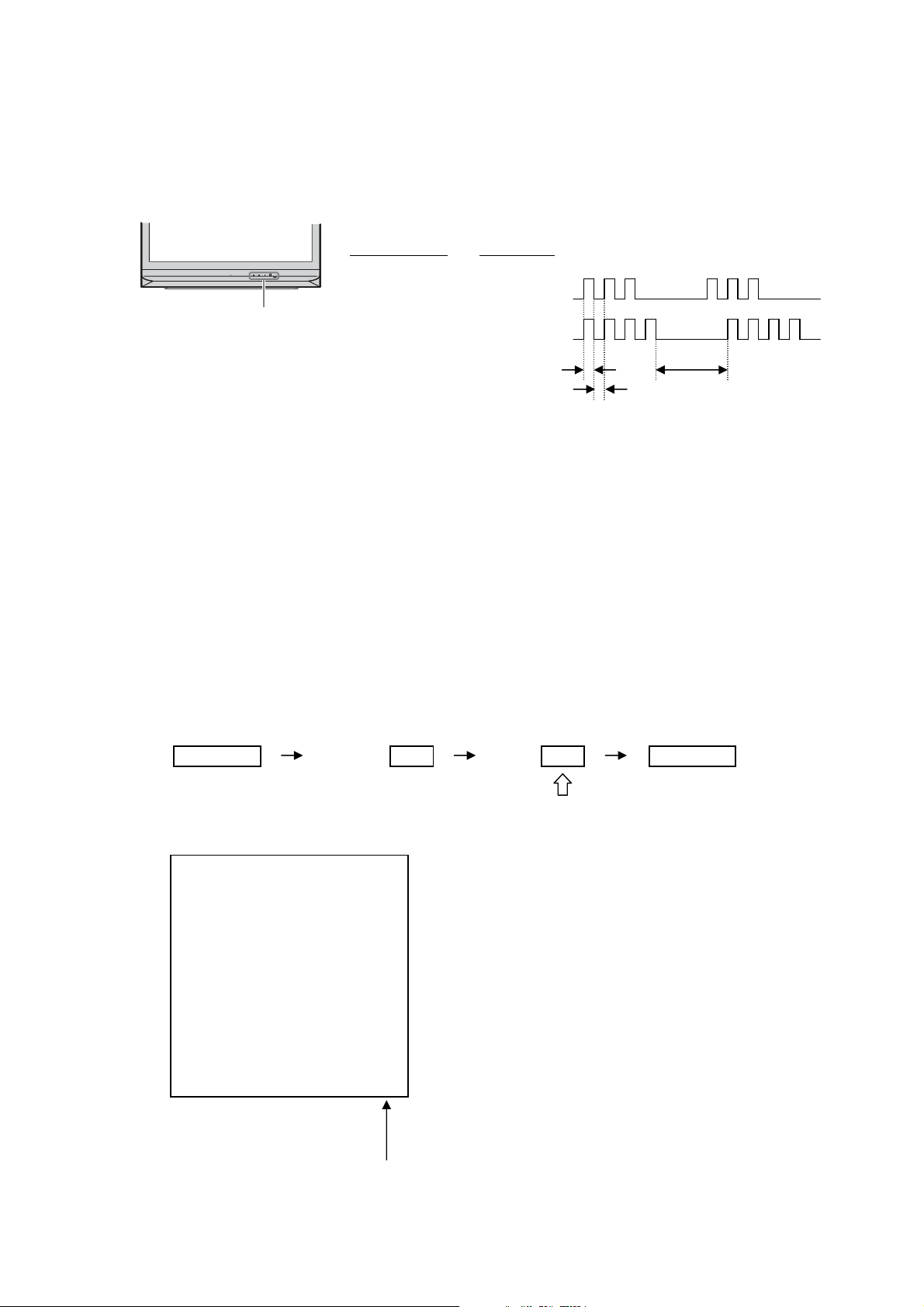
Indicators
KDF-E42A10/E50A10
K RM-YD003 RM-YD003
Screen
POWER/ST
TIMER LAMP
ANDBY
PUSH OPEN
Indicators
The indicators show the current status of your TV. If there is a change in the
condition or a problem with the TV, the indicators will flash or light up in
the manner described below to let you know that it requires your attention.
Indicator Flashing because...
POWER/
STANDBY flashing
LAMP indicator
flashes
TIMER indicator is
lit
green : The lamp for the light source is preparing to turn
on. When it is ready, it turns on.
red : The lamp door or the lamp is not securely attached.
The red indicator will continue to flash in intervals of three
blinks at a time until the lamp door or the lamp is placed
correctly. When the lamp door or the lamp is securely
attached, the TV will turn on with green indicator.
The projection lamp has burned out. Replace it with new
one (see page 86).
When one of the timers is set, the indicator will remain lit
(will not flash) even when the TV is turned off.
POWER
Projection Lamp
Your T V u ses a projection lamp as its light source. As with any lamp, it has
lifespan and needs to be replaced when the Lamp indicator flashes or the
screen becomes darker. Note the following:
After turning on your TV, it may take a while (1 minute or less) before
the picture appears.
When the projection lamp wears out, the screen goes dark. Replace the
lamp with a new Sony XL-2400 replacement lamp (not supplied).
The l
ight emitted from the lamp is quite bright when your TV i s i
use. To av
housing when
oid eye discomfort or injury, do not look into the light
the power is on.
n
– 4 –
Page 6
Replacing the Lamp
KDF-E42A10/E50A10
K RM-YD003 RM-YD003
The projection lamp, which illuminates the picture, has a limited life.
If the screen becomes dark, the color looks unusual, or the LAMP indicator
on the front of the TV flashes, it is time to replace the lamp with a new one
(not supplied).
WARNING
Electric appliances can cause fire or high temperature, resulting in
injury or death. Be sure to follow the instructions below.
Use a Sony XL-2400 replacement lamp (not supplied) for replacement.
Use of any other lamp may damage the TV.
Do not remove the lamp for any purpose other than replacement. Doing
so may cause injury or fire.
Do not put flammable materials and metal objects inside the lamp
receptacle of the TV after removing the lamp. Doing so may cause fire
or electrical shock. Do not touch the lamp receptable once the lamp has
been removed.
When the lamp eventually burns out, you may hear a noticeable pop
sound. This is normal and it is inherent to this type of lamp.
In rare instances, the bulb may pop inside the lamp unit, but the lamp
unit is designed to contain all of the broken glass pieces inside the lamp
unit.
The lamps contain mercury. For proper disposal of the used lamps,
follow and observe the local ordinances. See page 89.
How to Replace the
Lamp
1
Turn off the power on the main unit. Wait several minutes, then unplug
the power cord.
(The cooling fan will continue to operate for about two minutes after
turning the power off.)
2
Wait at least 30 minutes after unplugging the power cord to allow the
lamp to cool down before replacing it. To a
touch the lamp receptable once the lamp has been removed.
3
Take th e new lamp out of the box.
Do not touch the glass portion of the new lamp.
Do not
shake the lamp. Vi bration can damage the lamp or
shorten its
Avoid t
the lamp rec
life.
life.
ouching the front glass of a new lamp or the glass of
eptacle. Th is may reduce picture quality or lamp
void being burned, do not
– 5 –
Page 7
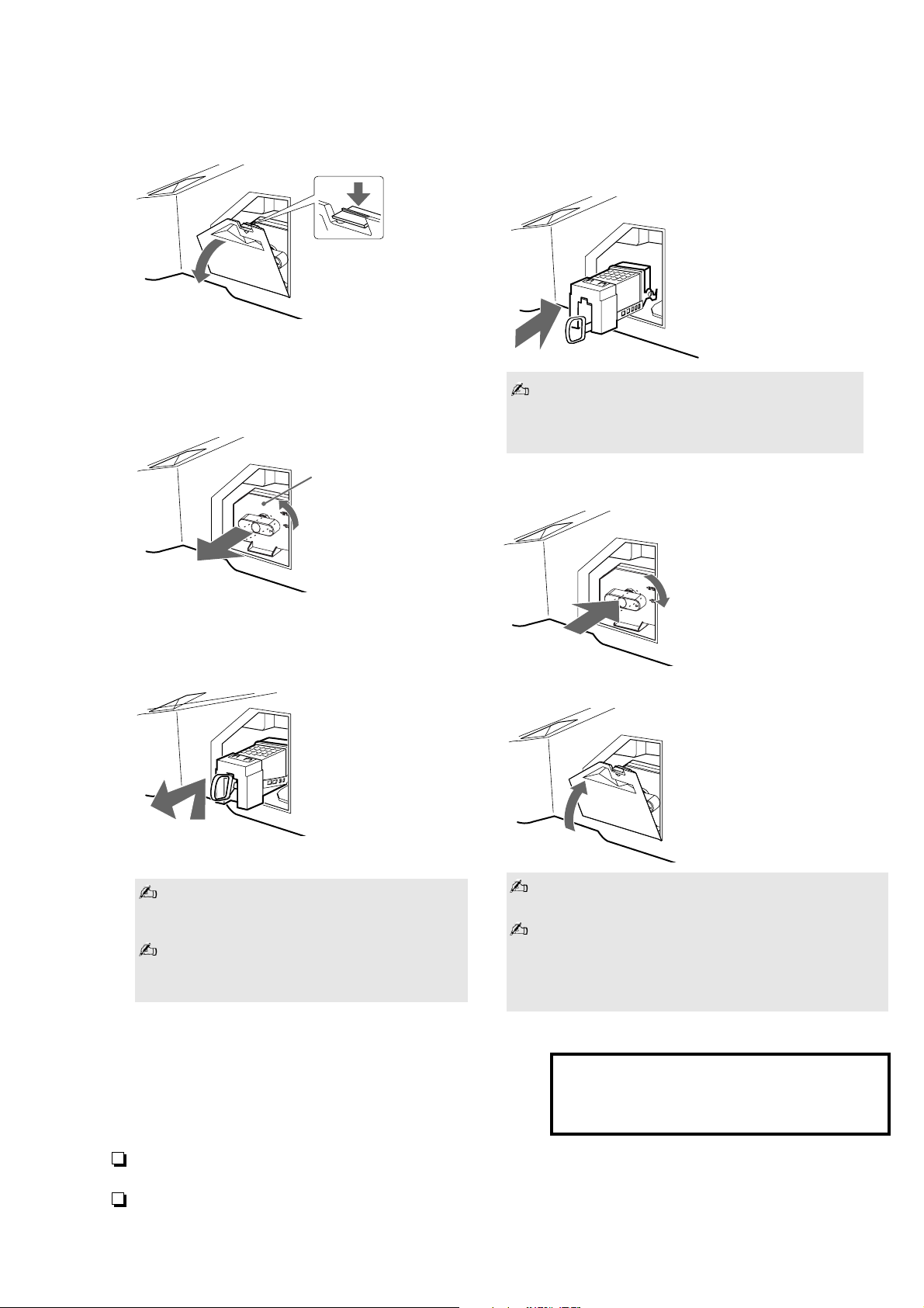
4 Remove the outside lamp cover.
KDF-E42A10/E50A10
K RM-YD003 RM-YD003
7
Put the new lamp into its place.
Mount the new lamp securely. Failure to do so may cause
a fire or the
screen to go dark.
5 Remove the lamp door.
Turn the knob counterclockwise to OPEN and pull out
the cover.
Lamp door
6 Pull out the lamp.
Hook a finger through the loop of the lamp handle and
pull the handle
upwards. Then pull the lamp straight out.
If the lamp is not securely reattached, the self-
di a gnostic
POWER/STANDBY indicator
times (see page 12).
8
Reattach the lamp door.
Turn the knob back to CLOSE and secure the cover.
9
Put the outside lamp cover back in its place.
function may be triggered and the
flashes three
The l
amp is very hot immediately after use.
Never touch the
the surrounding parts.
After
the used lamp has cooled, place it into
the empty box of
Never put the used lamp into a plastic
The used lamp
This product contains mercury.
regulated if
information,
Industries Alliance
Do not leave the used lamp near flammable materials or
within the
Do not pour water onto the used lamp or put any object
inside the lamp.
sold in the United States. For disposal or recycling
please
reach of children.
glass port
the replacem
contact your local authorities or
(http://www.eiae.org).
Doing so may cause the lamp to burst.
ion of the lamp or
ent lamp.
Disposal of this product may be
bag.
the Electronics
– 6 –
Consult you
replacement
Take gr eat c
in/un
plugging the connecting cords. Rough handling
may
cause the TV to fall, damaging the TV, the TV
st
and and the
For replacement lamp information visit:
U. S. residents: http://www.sonystyle.com/tv/
Canadian residents: http://www.sonystyle.ca/tv/
r Sony dealer for a Sony XL-2400
lamp.
are when replacing the lamp or plugging
floor.
Page 8
K RM-YD003 RM-YD003
Fig. B. Checking for earth ground.
Trouble Light
AC Outlet Box
Ohmmeter
Cold-water Pipe
SAFETY CHECK-OUT
( US model only )
KDF-E42A10/E50A10
After correcting the original service problem, perfom the follow-
ing safety checks before releasing the set to the customer:
l. Check the area of your repair for unsoldered or poorly-sol-
dered connections. Check the entire board surface for solder
splashes and bridges.
2. Check the interboard wiring to ensure that no wires are
“pinched” or contact high-wattage resistors.
3. Check that all control knobs, shields, covers, ground straps,
and mounting hardware have been replaced. Be absolutely
certain that you have replaced all the insulators.
4. Look for unauthorized replacement parts, particularly transistors, that were installed during a previous repair. Point them
out to the customer and recommend their replacement.
5. Look for parts which, through functioning, show obvious
signs of deterioration. Point them out to the customer and
recom mend their replacement.
6. Check the line cords for cracks and abrasion. Recommend
the replacement of any such line cord to the customer.
7. Check the condition of the monopole antenna (if any). Make
sure the end is not broken off, and has the plastic cap on it.
Point out the danger of impalement on a broken antenna to
the customer, and recommend the antenna’s replacement.
8. Check the B+ and HV to see they are at the values specified.
Make sure your instruments are accurate;be suspicious of
your HV meter if sets always have low HV.
9. Check the antenna temminals, metal trim, “metallized” knobs,
screws, and all other exposed metal parts for AC leakage.
Check leakage as described below.
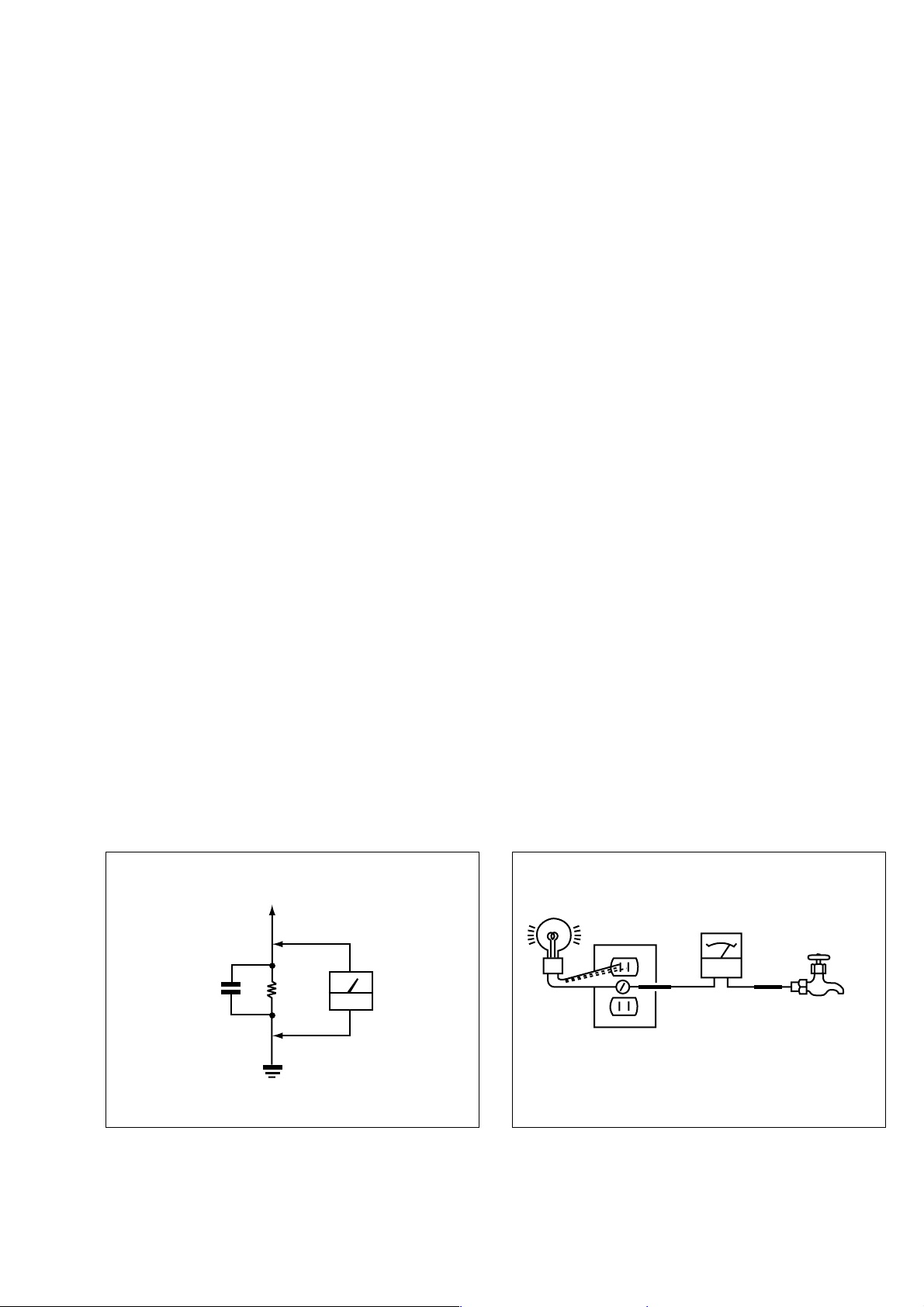
LEAKAGE TEST
The AC leakage from any exposed metal part to earth ground and
from all exposed metal parts to any exposed metal part having a
return to chassis, must not exceed 0.5mA (500 microampers) . Leakage current can be measured by any one of three methods.
1. A commercial leakage tester, such as the Simpson 229 or
RCA WT-540A. Follow the manufacturers’ instructions to
usc these instruments.
2. A battery-operated AC milliammeter. The Data Precision 245
digital multimeter is suitable for this job.
3. Measuring the voltage drop across a resistor by means of a
VOM or battery-operated AC voltmeter. The “limit” indication is 0.75V, so analog meters must have an accurate lowvoltage scale. The Simpson 250 and Sanwa SH-63Trd are
examples of a passive VOM that is suitable. NearIy all battery operated digital multimeters that have a 2V AC range
are suitable. (See Fig. A)
HOW TO FIND A GOOD EARTH GROUND
A cold-water pipe is guaranteed earth ground;the cover-plate retaining screw on most AC outlet boxes is also at earth ground. If
the retaining screw is to be used as your earth-ground, verify that it
is at ground by measuring the resistance between it and a coldwater pipe with an ohmmeter. The reading should be zero ohms. If
a cold-water pipe is not accessible, connect a 60-l00 watts trouble
light (not a neon lamp) between the hot side of the receptacle and
the retaining screw. Try both slots, if necessary, to locate the hot
side of the line, the lamp should light at normal brilliance if the
screw is at ground potential. (See Fig. B)
Fig. A. Using an AC voltmeter to check AC leakage.
1.5 µ F
To Exposed Metal
Parts on Set
1.5k Ω
Earth Ground
AC
voltmeter
(0.75V)
– 7 –
Page 9

KDF-E42A10/E50A10
K RM-YD003 RM-YD003
CAUTION
These servicing instructions are for use by qualified service personnel only.
To reduce the risk of electric shock, do not perform any servicing
other than that contained in the operating instructions unless you
are qualified to do so.
WARNING!!
AN ISOLATION TRANSFORMER SHOULD BE USED DURING
ANY SERVICE TO AVOID POSSIBLE SHOCK HAZARD, BECAUSE OF LIVE CHASSIS.
THE CHASSIS OF THIS RECElVER IS DIRECTLY CONNECTED
TO THE AC POWER LINE.
SAFETY-RELATED COMPONENT WARNING!!
COMPONENTS IDENTIFIED BY SHADING AND MARK ! ON THE
SCHEMATIC DIAGRAMS, EXPLODED VIEWS AND IN THE
PARTS LIST ARE CRITICAL TO SAFE OPERATION. REPLACE
THESE COMPONENTS WITH SONY PARTS WHOSE PART NUMBERS APPEAR AS SHOWN IN THIS MANUAL OR IN SUPPLEMENTS PUBLISHED BY SONY. CIRCUIT ADJUSTMENTS THAT
ARE CRITICAL TO SAFE OPERATION ARE IDENTIFIED IN THIS
MANUAL. FOLLOW THESE PROCEDURES WHENEVER CRITICAL COMPONENTS ARE REPLACED OR IMPROPER OPERATION IS SUSPECTED.
ATTENTION!!
AFIN D’EVITER TOUT RISQUE DELECTROCUTION PROVENANT D’UN CHÁSSIS SOUS TENSION, UN TRANSFORMATEUR
D’ISOLEMENT DOIT ETRE UTILISÉ LORS DE TOUT DEPANNAGE.
LE CHÁSSIS DE CE RECEPTEUR EST DIRECTEMENT RACCORDÉ Á L’ALIMENTATION SECTEUR.
ATTENTION AUX COMPOSANTS RELATIFS ÁLA
SÉCURITÉ!!
LES COMPOSANTS IDENTIFIÉS PAR UNE FRAME ET PAR UNE
MAPQUE ! SUR LES SCHÉMAS DE PRINCIPE, LES VUES EXPLOSÉES ET LES LISTES DE PIECES SONT D’UNE IMPORTANCE
CRITIQUE POUR LA SÉCURITÉ DU FONCTIONNEMENT. NE LES
REMPLACER QUE PAR DES COMPOSANTS SONY DONT LE
NUMÉRO DE PIÉCE EST INDIQUÉ DANS LE PRÉSENT MANUEL OU DANS DES SUPPLÉMENTS PUBLIÉS PAR SONY. LES
RÉGLAGES DE CIRCUIT DONT L’IMPORTANCE EST CRITIQUE
POUR LA SÉCURITÉ DU FONCTIONNEMENT SONT IDENTIFIES
DANS LE PRÉSENT MANUEL. SUIVRE CES PROCÉDURES
LORS DE CHAQUE REMPLACEMENT DE COMPOSANTS CRITIQUES, OU LORSQU’UN MAUVAIS FONCTIONNEMENT SUSPECTÉ.
– 8 –
Page 10

K RM-YD003 RM-YD003
TABLE OF CONTENTS
KDF-E42A10/E50A10
Section Title Page
–––––– –––– ––––
1. SELF DIAGNOSIS FUNCTION ..................... 11
2. DISASSEMBLY
2-1. Rear Cover .......................................................... 16
2-2. Service Position .................................................. 17
2-3. Antenna Switch, QU Block Assembly .............. 18
2-4. K Board............................................................... 19
2-5. Terminal Bracket ................................................ 19
2-6. HPC Board .......................................................... 19
2-7. B Block ............................................................... 20
2-8. OU Bracket ......................................................... 20
2-9. B Board ............................................................... 20
2-10. B, QM and QT Boards ....................................... 21
2-11. QT Board ............................................................ 21
2-12. QM Board ........................................................... 21
2-13. P Board ............................................................... 21
2-14. AGU Board ......................................................... 22
2-15. DC Fan ................................................................ 22
2-16. Main Duct (R) .................................................... 23
2-17. Duch Block Assembly
(Without Main Duct (R)) ................................... 23
2-18. D.C. Fan (Sirocco) ............................................. 23
2-19. Speaker Grill Block Assembly ........................... 23
2-20. HA and HB Boards ............................................ 24
2-21. Screen Frame Block Assembly .......................... 24
2-22. Speakers .............................................................. 24
2-23. Rear Cover (With Mirror) .................................. 24
2-24. How to Replace Optics Unit .............................. 25
2-24-1. Remove Lamp Bloxk (1) ............................ 25
2-24-2. Remove Lamp Bloxk (2) ............................ 25
2-24-3. Remove Lamp Bloxk (3) ............................ 25
2-24-4. Remove Cover, Rear (1) ............................. 25
2-24-5. Remove Cover, Rear (1-2) .......................... 25
2-24-6. Remove Cover, Rear (2) ............................. 25
2-24-7. Remove Stay (L), Side ................................ 26
2-24-8. Pull Out Some Blocks (1) ........................... 26
2-24-9. Pull Out Some Blocks (2) ........................... 26
2-24-10. Pull Out Some Blocks (3) ........................... 26
2-24-11. Pull Out Some Blocks (4) ........................... 26
2-24-12. Pull Out Some Blocks (5) ........................... 27
2-24-13. Pull Out Some Blocks (6) ........................... 27
Section Title Page
–––––– –––– ––––
2-24-14. Pull Out Some Blocks (7) ........................... 27
2-24-15. Pull Out Some Blocks (8) ........................... 28
2-24-16. Pull Out Some Blocks (9) ........................... 28
2-24-17. Pull Out Some Blocks (10) ......................... 28
2-24-18. Remove Optics Unit .................................... 28
3. ELECTRICAL ADJUSTMENTS
3-1. Electrical Adjustment by Remote Commander .... 29
3-1-1. Method of Setting the Service Adjustment
Mode ............................................................... 29
3-1-2. Service Mode Adjustment ............................ 29
3-1-3. Memory Write Confirmation Method .......... 29
3-1-4. Adjusting Buttons and Indicator ................... 29
3-2. To read Lamp and Panel time ............................ 30
3-3. Test Reset ........................................................... 30
4. DIAGRAMS
4-1. Block Diagram (1) .............................................. 31
Block Diagram (2) .............................................. 32
Block Diagram (3) .............................................. 33
Block Diagram (4) .............................................. 34
Block Diagram (5) .............................................. 35
Block Diagram (6) .............................................. 36
Block Diagram (7) .............................................. 37
4-2. Frame Schematic Diagram ................................. 38
4-3. Circuit Boards Location ..................................... 39
4-4. Schematic Diagrams ........................................... 39
(1) Schematic Diagram of GT Board ...................... 40
(2) Schematic Diagram of HA Board ..................... 41
(3) Schematic Diagram of HB Board ..................... 42
(4) Schematic Diagram of HC Board ..................... 43
(5) Schematic Diagram of K Board ......................... 44
(6) Schematic Diagram of QT (1/3) Board ............ 45
(7) Schematic Diagram of QT (2/3) Board ............ 46
(8) Schematic Diagram of QT (3/3) Board ............ 47
(9) Schematic Diagram of QU Board ..................... 48
(10) Schematic Diagram of S2 Board ........................ 49
(11) Schematic Diagram of T1 Board ....................... 50
(12) Schematic Diagram of T2 Board ....................... 51
– 9 –
Page 11

Section Title Page
–––––– –––– ––––
4-5. Printed Wiring Boards........................................ 52
(1) GT Board ............................................................ 52
(2) HA, HB Boards .................................................. 53
(3) HC, K Boards ..................................................... 54
(4) QT Board ............................................................ 55
(5) QU Board............................................................ 56
(6) S2 Board ............................................................. 57
(7) T1, T2 Boards ..................................................... 58
4-6. Semiconductors .................................................. 59
5. EXPLODED VIEWS
5-1. Screen Mirror Block, Cover ............................... 60
5-2. B Block, Chassis Assembly ............................... 61
5-3. Lamp Duct Assembly, Optics Unit Block ......... 62
KDF-E42A10/E50A10
K RM-YD003 RM-YD003
6. ELECTRICAL PARTS LIST
• GT Board .................................................................. 63
• HA Board .................................................................. 65
• HB Board .................................................................. 65
• HC Board .................................................................. 66
• HPC Board ................................................................ 66
• K Board ..................................................................... 67
• QT Board .................................................................. 69
• QU Board .................................................................. 71
• S2 Board .................................................................... 71
• T1 Board ................................................................... 71
• T2 Board ................................................................... 71
– 10 –
Page 12
SECTION 1
r
K RM-YD003 RM-YD003
SELF DIAGNOSIS FUNCTION
1. Summary of Self-Diagnosis Function
-This device includes a self-diagnosis function.
-Incaseofabnormalities, the POWER/STANDBY indicator automatically blinks. It is
possible to predict the abnormality location by the number of blinks. The Instruction
Manual describes blinking of the POWER/STANDBY indicator.
-Ifthe symptom is not reproduced sometimes in case of a malfunction, there is recording of
whether a malfunction was generated or not. Operate the remote command to confirm the
matter on the screen and to predict the location of the abnormality.
2. Diagnosis Items and Prediction of Malfunction Location
-When a malfunction occurs the POWER/STANDBY indicator only blinks for one of the
following diagnosis items. In case of two or more malfunctions, the item which first
occurred blinks. If the malfunctions occurred simultaneously, the item with the lowe
blink count blinks first.
-The screen display displays the results regarding all the diagnosis items listed below.
Thedisplay "0" means that no malfunctions occurred.
KDF-E42A10/E50A10
Number of times
Diagnosis Item
POWER/STANDBY
indicator blinks
Temp error
La
mp cover error 3 times
2 times
Fanstopped 4 times
Lamp driver error 5 times
Low B error 6 times
Probable Cause
Location
Defected symptoms
- Set temperture is high.
- Temp sensor connector
is not attached securely.
-Nopicture/No sound
(CN7020 on HB board,
CN7180 on S2 board)
-L
amp cover is not
attached securely.
-Nopicture/No sound
-Lamp is not set securely.
-Fan 1-4
power is not
supplied. (AGU board)
-F
an connector is not
-Nopicture/No sound
attached securely.
-Fan caught wires or
harnesses.
-Lampdriver is faulty. - No picture/No sound
- B_12V is not
(GT board)
supplie
d.
-Nopicture/No sound
- Short-circuit of Audio power
supply line.
Audio error 7 times
D-
OVP error 8
ATSC OVP
times
10 times
Lamp error LAMP-LED flashes - No picture/No sound
-Blow out of fuse.
(PS3001 on K board)
-IC failure.
(IC3005 on K board)
-B -12V is over voltage.
(B board)
-Q_10.5V is over voltage.
(GT board)
-Lampfor the light
source burns out.
-Nopicture/No sound
-Nopicture/No sound
-Nopicture/No sound
– 11 –
Page 13
K RM-YD003 RM-YD003
m
r
m
m
3. Blinking count display ofPOWER/STANDBY indicator
-One blink is not used for self-diagnosis.
-Example
Diagnosis ite
POWER/STANDBY
TIMER LAMP
POWER
PUSH OPEN
Lamp cove
Indicators
Fan 4 times
-Release of POWER/STANDBY indicator blinking
The POWER/STANDBY indicatorblinking display is released by removing the plug fro
the power or leaving for 2 minutes.
LEDblinks
3 times
LEDON:0.3sec
LEDOFF : 0.3sec
KDF-E42A10/E50A10
LED OFF
3.0sec
4. Self-diagnosis screen displays
-Incases of malfunctions where it is not possible to determine the symptom such as when
the power goes off occasionally or when the screen disappears occasionally, there is a
screen display on whether the malfunction occurred or not in the past (and whether the
detection circuit operated or not) in order to allow confirmation.
<Screen Display Method>
-Quickly press the remote command button in the following order from the standby state.
DISPLAY 5 - POWER
ChannelVol
Be aware that thisdiffers fro
the method of entering the
service mode (Vol +).
SELF CHECK
1:LAMP_ERROR 0
2 : TEMP_ERROR 0
2 : LAMP_TEMP 0
3:LAMP_COVER 0
4:FAN_ERROR 0
5:LAMP_DRIVER 1
6:LOWB_ERROR 0
7:AUDIO_PROT 0
8:D_OVP 0
10 : ATSC_OVP 0
-Numeral "1" means a fault was detected one time
-Numeral "0" means that no fault was detected
– 12 –
Page 14

KDF-E42A10/E50A10
k
K RM-YD003 RM-YD003
-The results display is not automatically cleared. In case of repairs and after repairs, chec
the self-diagnosis screen and be sure to return the results display to "0".
-Ifthe results display is not returned to "0" it will not be possible to judge a new malfunction
after completing repairs.
<Method of Cle aring Results Display>
1. Power off (Set to the standby mode)
2. Channel Vol
DISPLAY 5 - POWER
3. Channel
<Method of Ending Self-Diagnosis Screen>
-When ending the self-diagnosis screen completely, turn the power switch OFF on the
remote commander or the main unit.
5. Self-Diagnosis function operation
2:Temp When the temperature sensor on the S2 board detects high temperature, or IIC
3:Lamp cover The rib at the back of the lamp cover closes the SW on the T1 board. The lamp
4:Fan Fan rotation is detected by ‘‘FAN-PROT” and the TV-micro (pin 38 of IC8002)
8ENTER
line connector (CN8410:AGU board, CN7180:S2 board) is not seated securely,
the TV-micro tums off the lamp.
When the temperature sensor on the HB board detects high temperature, or IIC
line connector (CN8004:AGU board, CN7020:HB board) is not seated securely,
the TV-micro tums off the lamp.
closes the SW on the T2 board.
It is monitored by the BE micro (pin133 of IC4100) and tums off the lamp when
it is opened.
tums off the lamp when it is ‘‘high”.
5:Lamp Driver When the ‘‘LAMP-PROT” (pin132 of IC4100) is high, the lamp is not tumed
on. If the ‘‘LAMP-HV-DET” (pin134 of IC4100) is low at the same time, it
is classified as no high voltage of the lamp driver.
6:Low B error When no ‘‘B_12V” is detected, pin 128 of TV-micro is low and it tums off the
main power.
7:Audio When DC voltage is detected at the speaker output, pin 149 of TV-micro is low
and it tums off the main power.
8:D-OVP When overvoltage of ‘‘B_12V” is detected, pin 127 of TV-micro is low and it
tums off the main power.
10 : ATSC-OVP When overvoltage of ‘‘Q_10.5 V” is detected, pin 126 of TV-micro is low
and it tums off the main power.
LAMP : Lamp When the ‘‘LAMP-PROT” (pin132 of IC4100) is high, the lamp is not tumed
on. If the ‘‘LAMP-HV-DET” (pin134 of IC4100) is high at the same time, it
is classified as no lamp or a dead lamp.
– 13 –
Page 15
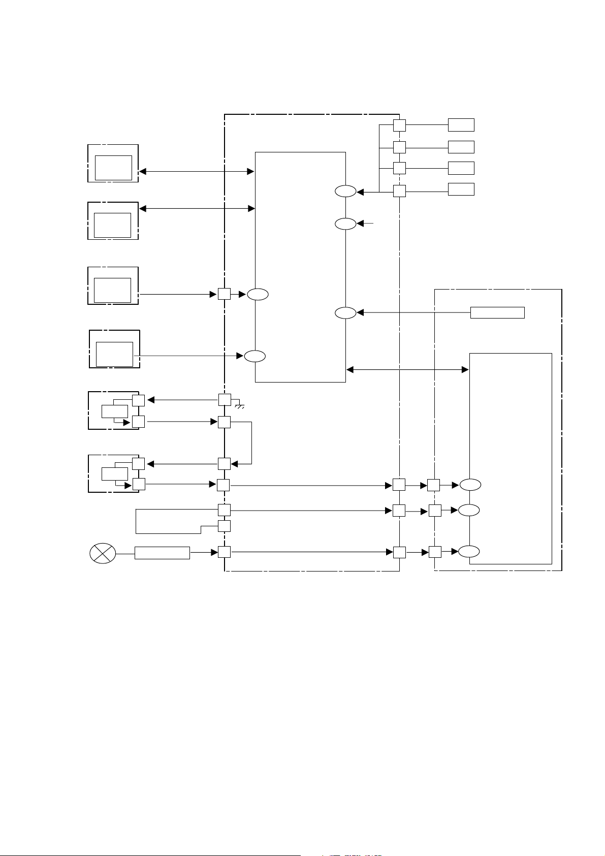
BLOCK DIAGRAM
KDF-E42A10/E50A10
K RM-YD003 RM-YD003
AGU board
S2 board
IC7180
Temp.
Sensor
HB board
IC7021
Temp.
Sensor
K board
Audio
Amp.
QM board
ATSC
10.5V
T2 board
SW
IC8002
TV Micro-computer
IIC-TV
FAN-ERR
IIC-TV
LB-ERR
13
CN8403
3
1
149
SP_PROT
BE-OVP
ATSC-OVP
126
2
1
38
128
127
IIC
4
7
10
13
CN8002
+12V
Fan1
Fan2
Fan3
Fan4
B board
B_12V
IC4100
BE Micro-computer
IIC
T1 board
SW
Lamp
1
3
HV-DET
Lamp Driver
CN8410
CN8410
CN8410
14
15
13
12
CN8003
8
5
CN8003
CN8003
7
7
8
5
7
133
LAMP COVER
134
LAMP-HV-DET
132
LAMP-PROT
– 14 –
Page 16
KDF-E42A10/E50A10
K RM-YD003 RM-YD003
Reading Lamp and Panel time
Use the following to determine the lamp and panel time of a set.
Screen Display Method
In standby mode, press the buttons on the Remote Commander sequentially, in rapid succession, as shown below:
1. Press Display , Channel 5 , Sound Volume + , Power ON
2. To enter BE-micro service menu, press JUMP 2 times.
3. To display the lamp time, press Channel-4.
The screen displays:
“ Total lamp time is 14 hours”
4. To display the panel time, press Channel-4.
The screen displays:
“ Total panel time is 14 hours”
5. To display the lamp time clear, press Channel-5
7 times and Channel-1.
To reset the lamp time press Channel-3 > MUTING > ENT.
WRITE (Character color is red) is momentarily displayed and the lamp time is reset to “0”.
Exiting Service Mode
After completing the changes exit service mode by turning off the set using the Remote Commander or the
power switch.
CONFIGRATION 00 SERVICE
CP18_COLOR_SYS 00 00A0 BE Micro
Press Channel-4
m
GW_SPECIAL 34 SERVICE
LAMP_TIME 02 00000014 BE Micro
Press Channel-4
m
GW_SPECIAL 34 SERVICE
PANEL_TIME 01 00000014 BE Micro
Press Channel-5 7 times,
m
Channel-1
OPTION_E 20 SERVICE
LAMP 01 0000 BE Micro
– 15 –
Page 17
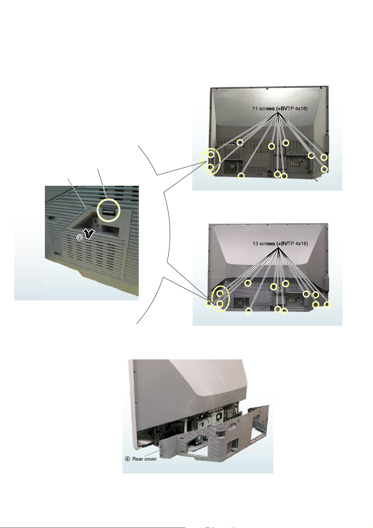
2-1. REAR COVER
3
3
1 Pull down the claw
Lamp door
SECTION 2
DISASSEMBLY
E42A10
KDF-E42A10/E50A10
K RM-YD003 RM-YD003
E50A10
– 16 –
Page 18
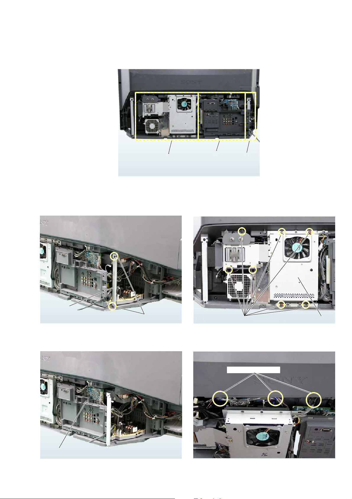
2-2. SERVICE POSITION
A
C
B
4
)
5
lightl
holders
KDF-E42A10/E50A10
K RM-YD003 RM-YD003
A
3 Side stay (L)
C
1 2 screws (+BVTP 4x16)
B
7 screws (+BVTP 4x16
n wire
ull out B block s
y
6 Pull out chassis block slightly
– 17 –
Page 19
8 Loosen wire holders
)
backward
)
)
itch bracket
y
KDF-E42A10/E50A10
K RM-YD003 RM-YD003
K board assembly
2-3. ANTENNA SWITCH, QU BLOCK ASSEMBLY
crew (+BVTP 4x16
crew (+BVTP 4x16
9 Tu rn chassis dssembly
GT board B side
cover
6 Antenna switch
crew (+BVTP 4x16
5 5 connectors
2 hexdgonal washers
a
s
U block assembl
ntenna sw
– 18 –
Page 20
2-4. K BOARD
KDF-E42A10/E50A10
K RM-YD003 RM-YD003
1 2 screws (+BVTP 4x16)
2 Pull out K board assembly
6
5 2 screws (+BVTP 3x12)
3 3 connectors
4 2 screws (+BVTP 3x12)
K board
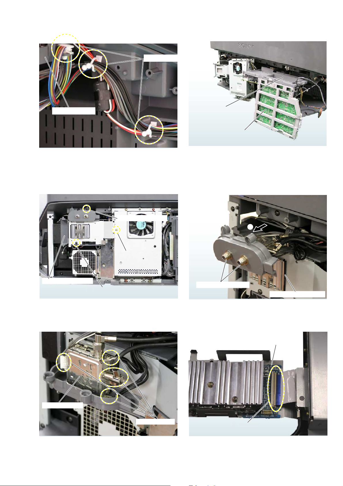
2-5. TERMINAL BRACKET
1 7 screws (+BVTP 3x12)
2
Te r mi nal brdcket
2-6. HPC BOARD
3
1 2 connectors
HPC baord
2 2 screws
(+PVTP 4x16)
Te r minal bracket
– 19 –
Page 21
ectors
block
ecto
block
ectors
()
)
et
s
)
)
ecto
board
2-7. B BLOCK
nn
KDF-E42A10/E50A10
K RM-YD003 RM-YD003
r
conn
2-8. OU BRACKET
6 screws (+PSW M 3x8
conn
brack
screw
(+PSW M3x8
2-9. B BOARD
conn
4 screws (+PSW M3x8
r
– 20 –
Page 22
)
a
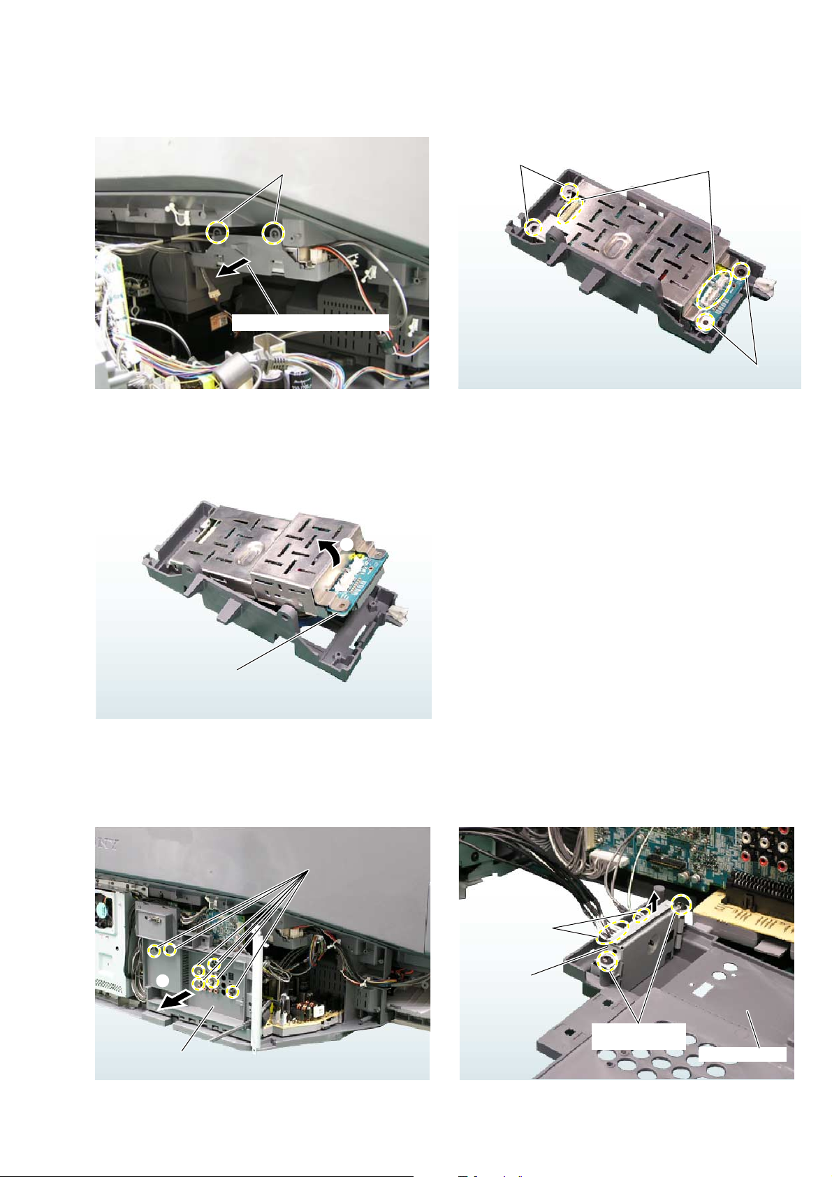
2-10. B, QM AND QT BOARDS
board
ecto
lid of shield
)
hield case (DIGITAL
KDF-E42A10/E50A10
K RM-YD003 RM-YD003
rdsB, QM and QT bo
2-11. QT BOARD
1 Place the pod bracket assembly
upside down.
2 3 connector
3 3 screws
(+PSW M3x8)
2-12. QM BOARD 2-13. P BOARD
T board
2 5 screws
er
(+PSW M3x8)
3 QM board
1 3 connectors
2 screws (+PSW M3x8
case
nn
r
AGU
– 21 –
Page 23
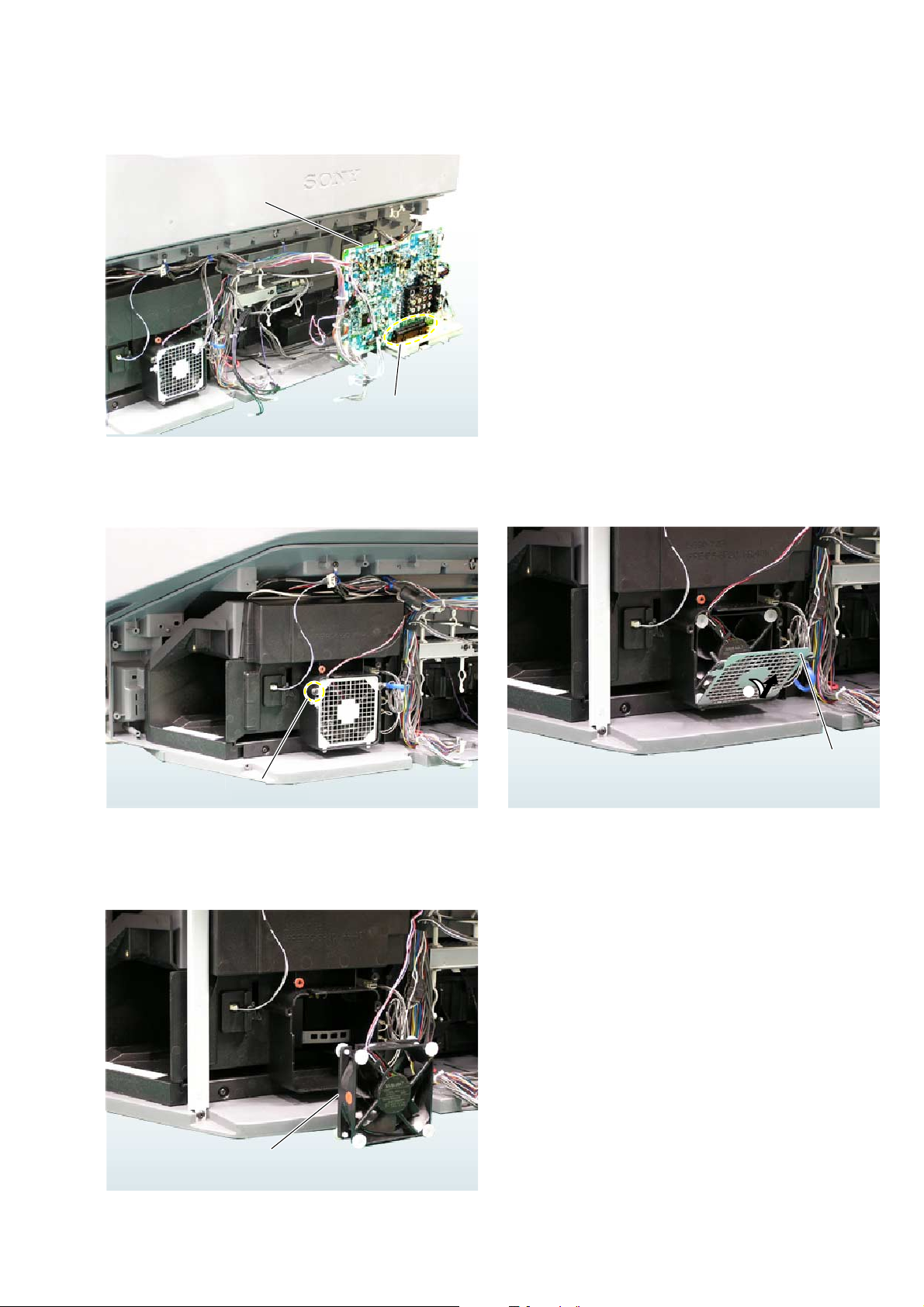
2-14. AGU BOARD
)
2 AUG board
2-15. DC FAN
KDF-E42A10/E50A10
K RM-YD003 RM-YD003
1 Connector
+BVTP 4x16
2
80 fan plate
DC fan
– 22 –
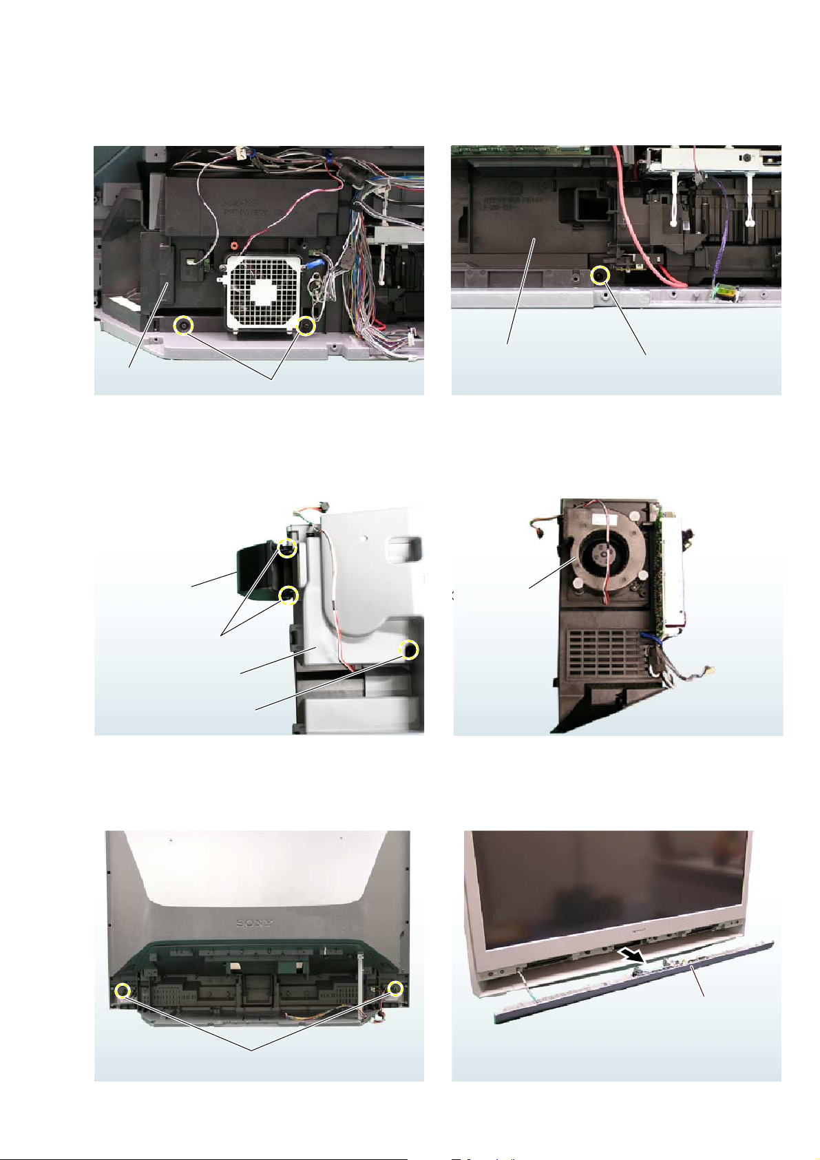
Page 24
KDF-E42A10/E50A10
K RM-YD003 RM-YD003
2-16. MAIN DUCT (R)
2 Pull out main duct (R)
2-18. D.C. FAN (SIROCCO)
1 2 screws (+BVTP 4x16)
2-17. DUCT BLOCK ASSEMBLY
(WITHOUT MAIN DUCT (R))
2 Pull out duct block assembly
1 Screw (+BVTP 4x16)
Lamp duct cover
1 2 claws
4 Remove SIROCCO
fan cover upward
3 Screw (+BVTP 4x16)
2-19. SPEAKER GRILL BLOCK ASSEMBLY
Remove D.C. fan
sirrocco) upward
2
1 2 screws
(+BVTP 4x16)
Speaker grill block assembly
– 23 –
Page 25
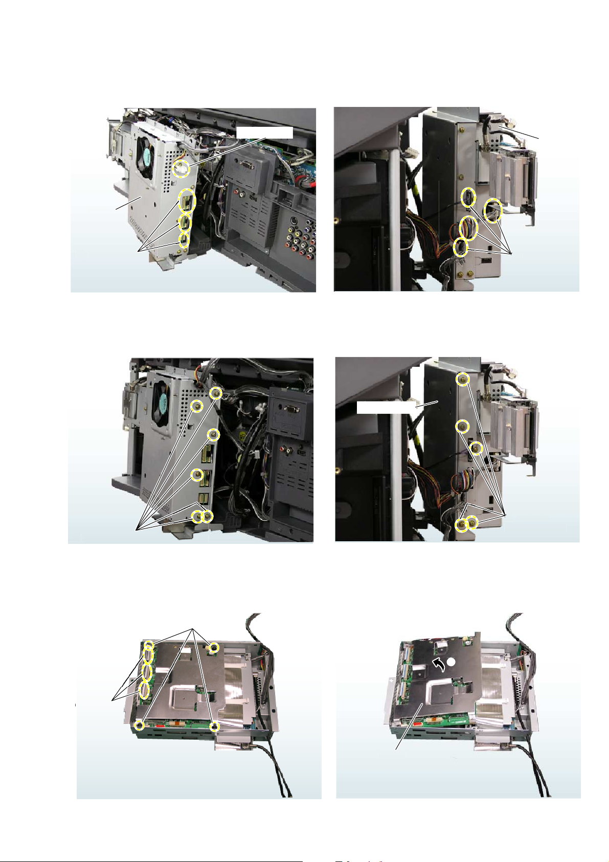
2-20. HA AND HB BOARDS
)
)
3 HA board
1 Connector
5 2 Screws
4 Connector
2 2 screws
(+BVTP 4x12)
2-21. SCREEN FRAME BLOCK ASSEMBLY
KDF-E42A10/E50A10
K RM-YD003 RM-YD003
3 Screen frame
x13) (E42A10
x13) (E50A10
2 4 screws
(+BVTP 4x16)
block assembly
2-22. SPEAKERS 2-23. REAR COVER (WITH MIRROR)
2 Rear cover (with mirror)
2 Speaker
1 2 screws
(+PWTP2 4x16)
Screen frame block assembly
4 Speaker
3 2 screws
(+PWTP2 4x16)
1 4 screws
(+BVTP 4x16)
– 24 –
Page 26
2-24. HOW TO REPLACE OPTICS UNIT
k
p
k
p
s
s
s
screws
ew
KDF-E42A10/E50A10
K RM-YD003 RM-YD003
2-24-1. Remove Lamp Block (1)
Remove '' Door, Lamp ".
Door, Lamp
A
< A > < REAR VIEW >
2-24-3. Remove Lamp Block (3)
Pull the "Lever, Lock" below to remove "Lamp block".
2-24-2. Remove Lamp Block (2)
Turn left "Lever, Lock" below, and then remove "Door, Lamp".
ever, Loc
oor, Lam
2-24-4. Remove Cover, Rear (1)
Take off 11 screws (42"), and then pull out "Cover, Rear".
2 screws
over, Rear
ever, Loc
2-24-5. Remove Cover, Rear (1-2)
oor, Lam
2-24-6. Remove Cover, Rear (2)
Take off 13 screws (50"). It is removed "Cover, Rear".
3 screws
screw
2 screws
screw
2 screws
B
screw
over, Rear
E
scr
2 screws
D
C
– 25 –
Page 27
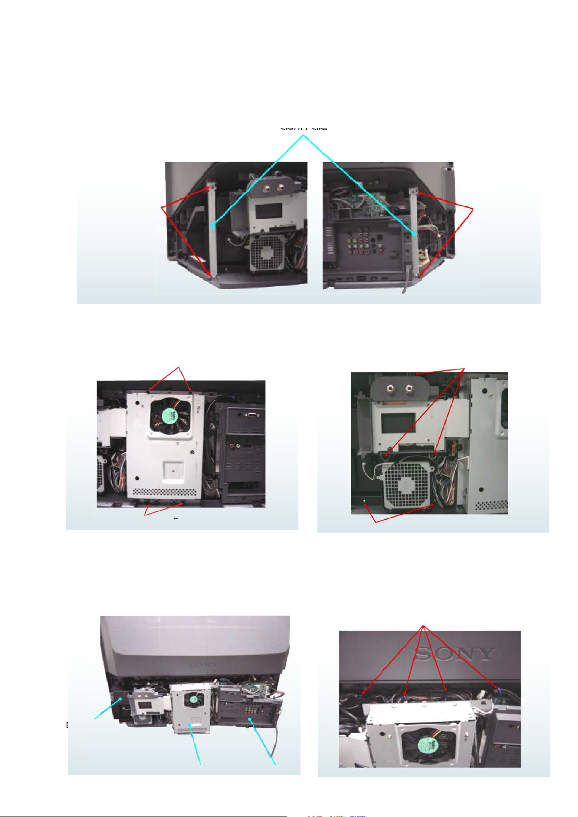
2-24-7. Remove Stay (L), Side
screws
s
Side (L)
s
screws
s
block
block
,
Take off 4 screws, and then remove 2 "Stay (L), Side".
KDF-E42A10/E50A10
K RM-YD003 RM-YD003
,
screw
2-24-8. Pull Out Some Blocks (1)
Take off 4 screws.
2 screws
< B >
< C >
2-24-9. Pull Out Some Blocks (2)
Take off 5 screws.
screw
screw
2-24-10. Pull Out Some Blocks (3)
Pull out "B block", "Chassis block", and "Duct (R), Main"
a little bit.
uct (R), Main
2-24-11. Pull Out Some Blocks (4)
Unlock "Holder, Wire" as shown below.
older, Wire
– 26 –
Page 28
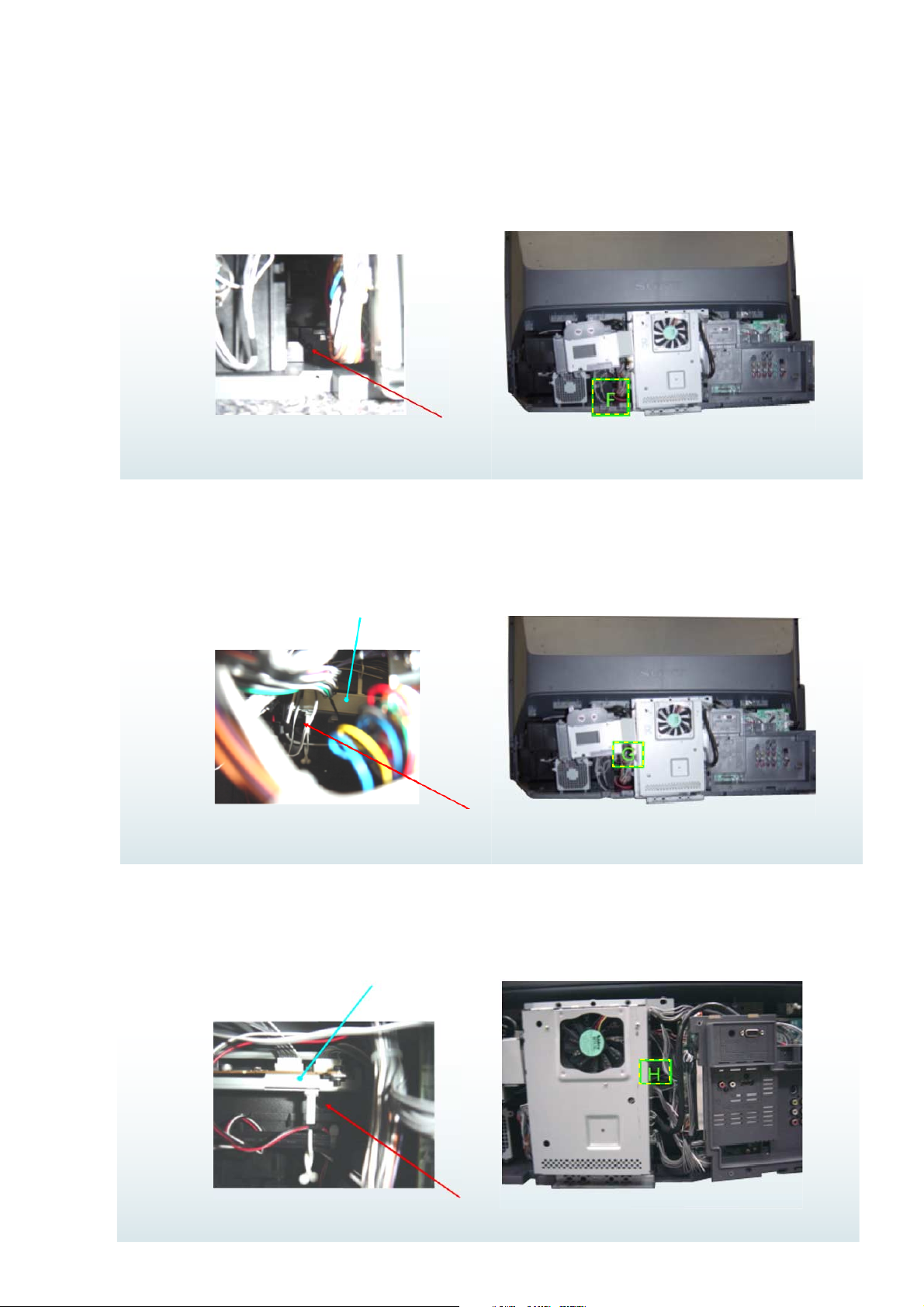
2-24-12. Pull Out Some Blocks (5)
Take off 1 screw.
< F >
KDF-E42A10/E50A10
K RM-YD003 RM-YD003
3 screws
F
1 screw
2-24-13. Pull Out Some Blocks (6)
Loose 1 special screw. (This screw can not be taken off.)
Optics unit block
< G >
2-24-14. Pull Out Some Blocks (7)
Take off 1 screw.
G
1 special screw
Optics unit block
< H >
H
1 special screw
– 27 –
Page 29
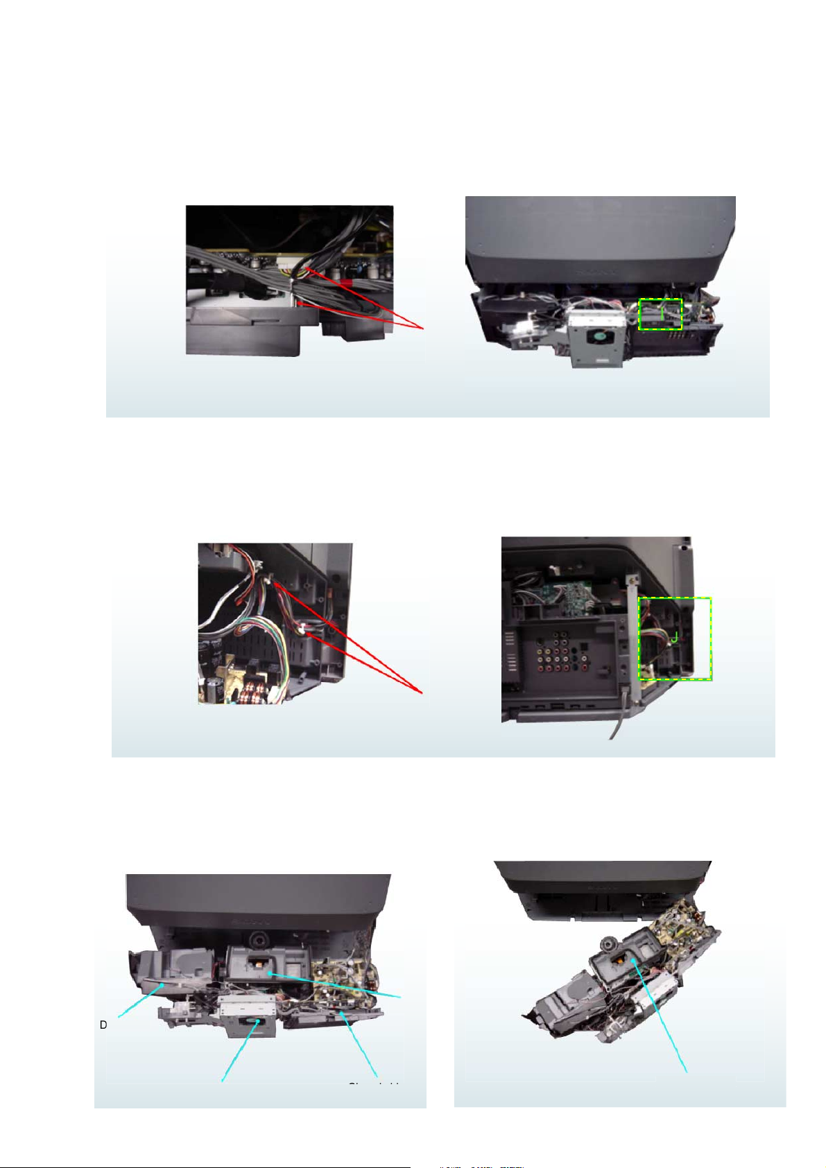
unit block
2-24-15. Pull Out Some Blocks (8)
k
u
block
Remove 2 connecters to pull out some blocks as shown below.
< I >
KDF-E42A10/E50A10
K RM-YD003 RM-YD003
I
Connector
2-24-16. Pull Out Some Blocks (9)
Unlock "Purse Lock" to pull out some blocks as shown below.
< J >
2-24-17. Pull Out Some Blocks (10)
Pull out "B block", "Chassis block", "Duct block", and "Optics
Unit block".
J
Purse lock
2-24-18. Remove Optics Unit
Remove all connecters to remove "Optics Unit block" and then it.
nit bloc
ics
B block
– 28 –
Page 30
SECTION 3
ELECTRICAL ADJUSTMENTS
3-1. ELECTRICAL ADJUSTMENT BY REMOTE
COMMANDER
By using remote commander (RM-YD003), all circuit adjust-
ments can be made.
NOTE : Test Equipment Required.
1. Pattern Generator (with component outputs)
2. Oscilloscope
3. Digital multimeter
3-1-1. Method of Setting the Service Adjustment
Mode
KDF-E42A10/E50A10
K RM-YD003 RM-YD003
3-1-2. Service Mode Adjustment
1. The SCREEN displays the item being adjusted.
2. Press “1” or “4” on the remote commander to select the
adjustment item.
3. Press “3” or “6” on the remote commander to change the data.
4. Press “2” or “5” on the remote commander to select the category.
Every time you press “2” (Category up).
5. If you want to recover the latest values press “-” then
“[ENTER]” to read the memory.
6. Press “[MUTING]” then “[ENTER]” to write into memory.
7. Turn power off.
1. Standby mode. (Power off)
2. DISPLAY t 5 t VOL (+) t TV POWER
on the remote commander.
(Press each button within a second.)
The following service screen will appear.
<TV micro>
STATUS 0 SERVICE
SHUTDOWN_LOG1 0 TV MICRO
ATI : H05-01.xx
SAIPH PROGRAM : 1.xxx
BOOT : x.xxx
CHIMERA PROGRAM : 1.xxx
PACK : 1.xxx
OSD : x.xxx
NVM A0 : x.xxx
NVM AC : x.xxx
NVM AE : ----
HDMI : 1.xxx
Press “JUMP” key.
<Digiotal Module micro>
QM 0 0 SERVICE
INFO DTV
Press “JUMP” key.
<BE micro>
<Method of setting the shipping condition>
1. Service Adjustment mode.
2. Press “8” then “[ENTER]”
3. Wait until appearing “ Initial Setup” display.
4. Disconnect AC plug and connect again to change factory re-
set condition completely.
3-1-3. Memory Write Confirmation Method
1. After adjustment, turn power off with the remote commander.
2. Turn power on and set to service mode.
3. Call the adjusted items again and confirm they were adjusted.
3-1-4. Adjusting Buttons and Indicator
MUTING
Adjustment item
up
Adjustment item
down
Initialize data
(Not stored)
User control goes
to the standerd state
(Shipping Conditions)
JUMP
VOL +
TV/VIDEO
POWER TV POWER
MUTING
DVD/
SAT/
VCR
CABLE
DVR
FUNCTION
JUMP ANT MTS/SAP FREEZE
SOUND PICTURE
TV/SAT
SUR
IDE
U
G
R
E
T
U
R
N
WEGA
E
T
A
G
REPLAY ADVANCE NEXTPREV
PLAY
VISUAL SEARCH
PAUS E
VOL
TV
ENT
WIDE
D
ISP
LA
Y
S
L
O
O
T
STOP
CH
TV POWER
Adjustment category
up
Data up
Data down
Adjustment category
down
ENTER
DISPLAY
CONFIGRATION 00 0 SERVICE
CP18_COLOR_SYS
00 00A0 BE Micro
Press “JUMP” key.
REC REC PAUSE REC STOP
TOP MENU MENU F1 F2
RM-YD003
– 29 –
Page 31

KDF-E42A10/E50A10
K RM-YD003 RM-YD003
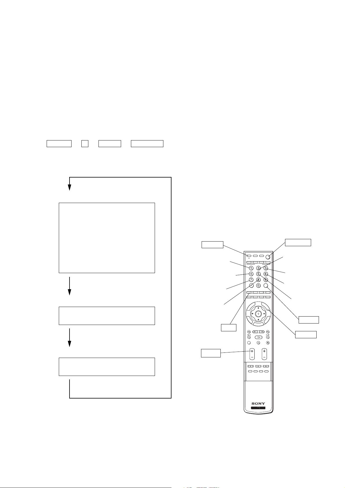
FUNCTION OF KEYS ON COMMANDER
• 1 : Changes adjustment item. (item No. moves up)
• 4 : Changes adjustment item. (item No. moves down)
• 2 : Changes adjustment category.
(category moves up)
• 5 : Changes adjustment category.
(category moves down)
• 3 : Changes data value. (up)
• 6 : Changes data value. (down)
Commander Function
Button Mode Description
[MUTING] + [ENTER] WRITE Writes data to NVM.
- + [ENTER] READ Reads data from NVM.
8 + [ENTER] RESET Set the shipping condition.
3-2. H/V Center Confirmation and Adjustment
Please check the picture horizontal/vertical center after the replace-
ment of the following parts .
• Optical block
• Top assembly
1, Check H/V center with 480i monoscope signal in “Full “ mode .
2, If the center is shifted , adjust it with the following service items .
3-3. IRIS Adjustment
Please check it after the replacement of the following parts.
• IRIS unit+Optics unit block+C board
• B board
Check values of the service data in NVM on C board
#0 BL_U_TOP
#1 BL_U_BOTTOM
DBL_CTRL_AC
and write the same values on C board to the service data in NVM
on B board.
DBL_CTRL
#2 BL_MAX
#3 BL_MIN
#4 IRIS_GAIN
#5 HALL_GAIN
#0 BL_U_TOP
#1 BL_U_BOTTOM
#2 BL_MAX
#3 BL_MIN
#4 IRIS_GAIN
#5 HALL_GAIN
ODHS (for H center)
ODVS (for V center)
ODHS
ODVS
– 30 –
Page 32

4-1. BLOCK DIAGRAM (1)
SECTION 4
DIAGRAMS
KDF-E42A10/E50A10
K RM-YD003 RM-YD003
Rear
Note:
AGU, B, HPC, P and QM boards are supplied as the block for service.
C board is included in the Optics Unit Block.
(The parts on each boards are not supplied individually.)
CXD9855GP
Rear
AGU
AK5357
CXA2188Q
CS4335
Rear
– 31 –
Left Side
Page 33

KDF-E42A10/E50A10
K RM-YD003 RM-YD003
BLOCK DIAGRAM (2)
TU7800
TUNER
DET_OUT
VHF/UHF
CABLE
TO
QM BOARD
CN7307
R_OUT
L_OUT
AFT_OUT
AGC_IN
TU_SDA
TU_SDA
TU_CLK
TU_CLK
12C_SW
FAT_LOCK
FDC_LOCK
DATA0/SDATA
MPEG_CLK
MPEG_ENA
CRX
DRX
RESET
DEM_SDA
DEM_CLK
MPEG_ERR
CN7800
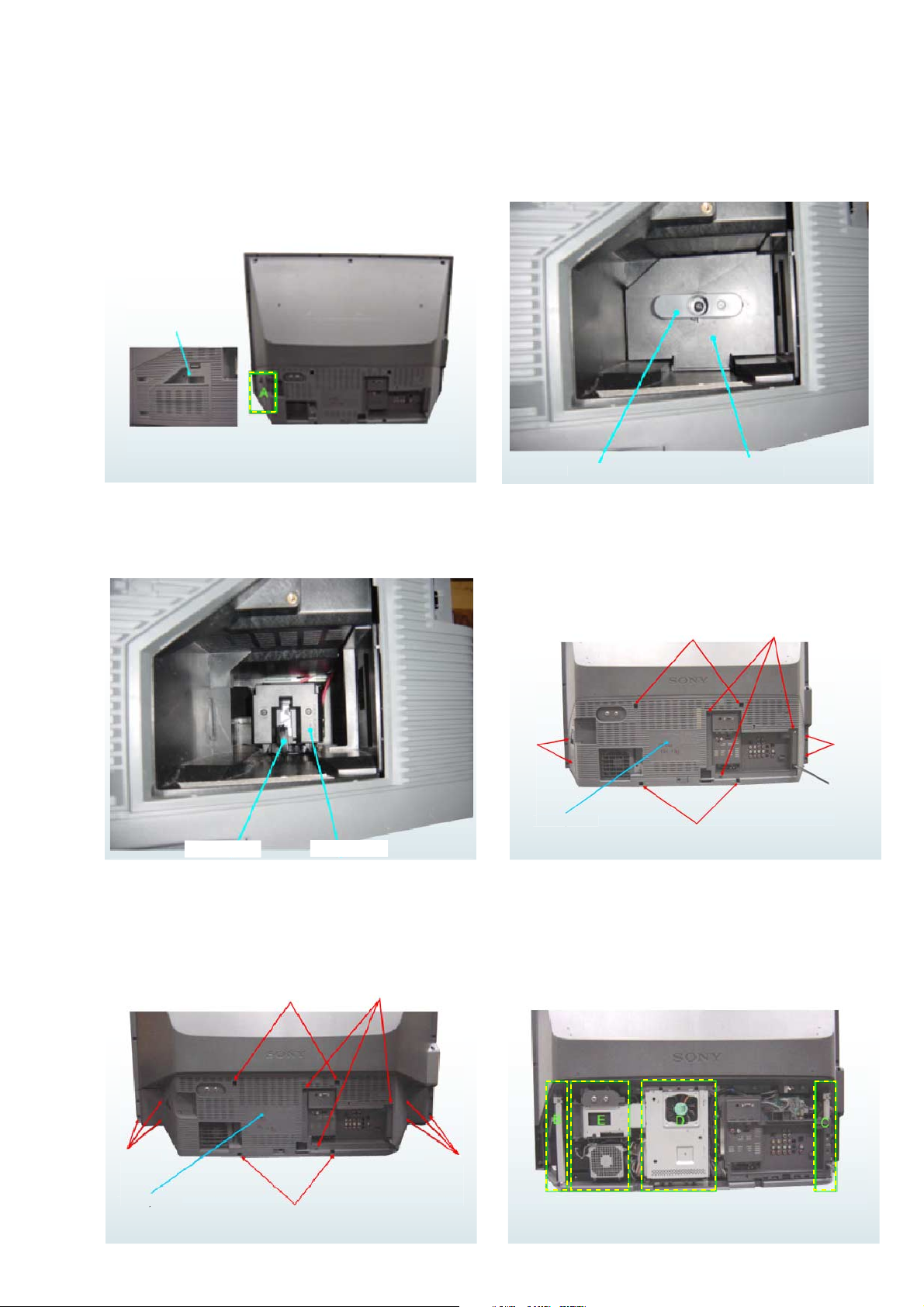
10.5V
6.0V
3.4V
1.5V
VIDEO VIDEO
AUDIO R
AUDIO L
RESTE_FE
FE_SDA
FE_SCL
2
4
6
8
Q7802
BUFFER
Q7803
AGC AMP
D7802
(FAT LOCK)
D7801
(FDC LOCK)
XPOD_STBY
Q7804,7805
LED DRIVER
Q7806,7807
B+ SWITCH
+10.5V
+6.0V
+3.4V
+1.5V
TO
QU BOARD
CN7951
CN7801
AUDIO R
AUDIO L
IC7806
NTSC/ATSC TUNING SELECT
Y
15
Y0 Y1
2
14
X
12
X0
11
10
9
32V DC/DC CONVERTER
VIN
1 4
OSC
2
VIN
1 5
ON/OFF
3
VIN
2 4
CTRL
1
VIN
2 4
CTRL
1
VIN
1 5
CE
3
VIN
4 5
VBIAS
2
A
B
C
D7803
(ERROR)
IC7804
IC7803
9V REG.
IC7802
5V REG.
IC7808
5V REG.
IC7801
1.8V REG.
IC7800
1.1V REG.
ENA/ADJ
X1
VOUT
VOUT
VADJ
VOUT
VOUT
VOUT
VOUT
1
13
DK
3
4
1
A
POD_VCC
POD_VCC
1
PODVCC
POD_VPP
TU_R_OUT
42597
AUDIO R
AUDIO L
PODVPP
TO
AGU BOARD
CN8006
AFT_OUT
TU_L_OUT
TU_V_OUT
101413
VIDEO
+32V
+9V
+5V
POD_5V
+1 .8V
+1.1V
TU_SCL
TU_SDA
12
AGC_MUTE
CN7802
SCLK
246
NCNCNC
TO
QM BOARD
CN7306
HD0
HD1
HD2
HD3
HD6
HD4
HD5
HD6
HD4
HD5
IC7807
DATA SWITCH
3
1Y
6
2Y
3Y
8
4Y
11
1OEN
1
4
2OEN
10
3OEN
13
4OEN
HD7
HD7
HACK
SDATA
FE_SCL
FE_SDA
RESTE_FE
AGC_MUTE/LRCLK
RESET_POD
8
1011121314161820222426283032343637383940424446
FE_SDA
HRESET#
FE_SCL
RESTE_FE
33M_CLK
HACKPOL
XPOD_STBY
XPOD_STBY
HACKPOL
33M_CLK
HIRQ#
HIRQ#
HACK#
TU_TSDATA
TU_TSCLK
TU_TSENA
TU_SSYNC
HD0
HD1
HD2
HD3
QT
CS#
HA1
HA0
HA1
1A
2A
3A
4A
HCS
12
HRW
HA0
HRW#
2
5
9
FF_SCLK
FE_SYNC
TU_TSDATA
TU_SSYNC
TU_TSCLK
FE_VAL
FE_SDATA
48
TU_TSENA
IC7906
HRW#
33M_CLK
HRESET#
HACKPOL
HIRQ#
HACK#
HD0
HD1
HD2
HD3
HD4
HD5
HD6
HD7
HA0
HA1
HCS
MPEG_SDATA
MPEG_CLK
MPEG_ENA
POD_5V
+3.4V
3
5
93
92
91
90
89
88
87
86
85
84
83
79
81
80
82
98
99
96
100
73
72
71
76
78
CLK
HRESET#
HACKPOL
HIRQ
HACK
HD0_SDA
HD1_SCL
HD2
HD3
HD4
HD5
HD6
HD7
HA0
HA1
HCS
HRW
TDO
TOCLK
TOVAL
TOSTRT
TID
TICLK
TIVAL
CRX
DRX
11
IC7900
POD INTERFACE
CONTROLLER
VPPSEL
IC7906
POWR SWITCH
2 7
IN1
4
EN1
IN2
3
5
EN2#
IC7906
POWR SWITCH
2,3
IN
4
EN#
CD2#
MDO2
MDO1
MDO0
MOSTRT
MOVAL
WAIT#
A4_CTX
RST
MDI7
MDI6
MDI5
MCLKI
MDI4
MIVAL
MDI3
IREQ#
MDI2
WE#
MDI1
MCK0
MDI0
MISTRT
A8_CRX
IOWR#
A9_DRX
IORD#
OE#
CE2#
MDO7
CE1#
MDO6
MDO5
MDO4
MDO3
CD1#
OUT
D2
D1
D0
A0
A1
A2
A3
A5
A6
A7
A11
A10
D7
D6
D5
D4
D3
OUT1
OUT2
70
69
58
68
57
67
56
66
54
65
55
52
53
64
51
63
48
46
62
47
61
60
45
59
44
28
43
26
42
25
41
23
21
40
20
39
19
37
35
18
34
17
33
16
32
15
31
14
29
13
30
12
27
6
5-8
PODVCC
PODVPP
PODVCC
(TUNER, POD INTERFACE CONTROLLER, POWER SUPLLY)
CN7903
3
CD2#
5
MDO2
D2
6
MDO1
7
D1
8
MDO0
9
D0
10
11
MOSTRT
13
A0
MOVAL
14
15
A1
A2
17
INPACK#
18
19
A3
21
WAIT#
A4_CTX
22
23
RESET
A5_ITX
24
A6_ETX
26
27
MDI7
A7_QTX
29
MDI6
30
A12
31
32
MDI5
33
MCLKI
34
MDI4
35
MIVAL
36
VPP-1, 2
40
41
VCC
45
MDI3
46
47
IREQ#
48
MDI2
49
WE#
MDI1
50
MCK0
51
MDI0
52
54
A13
MISTRT
55
56
A8_CRX
57
IOWR#
A9_DRX
58
59
IORD#
60
NC
A11
VS1#
62
63
OE#
64
CE2#
A10
65
MDO7
66
67
CE1#
MDO6
68
70
D7
71
MDO5
72
D6
73
MDO4
D5
74
75
MDO3
76
D4
77
CD1#
78
D3
B
TO
QU BOARD
CN7953
– 32 –
Page 34

BLOCK DIAGRAM (3)
KDF-E42A10/E50A10
K RM-YD003 RM-YD003
TO
AGU BOARD
CN8001
CN3002
SCSHIFT
SCDT
DF_FLAG
KCLATCH
LR_DATA
BCLK
LRCK
MCLK
AMP_RST
SP-PROT
3.3V_SW
IC3002 (1/2)
BUFFER
14A_MUTE
6M_RST
11
9
8
7
5
3
4
1
12
13
15
D+3.3V
5
4
IC3004
BUS BUFFER
2
4
3
6
8
7
9
11
IC3002 (2/2)
GATE
6
18
16
17
14
12
13
11
12
13
IC3006
PCM/PWM PROCESSOR
SOFTMUTE
19
INIT
27
22
SCSHIFT
SCDT
21
23
SCLATCH
31
DATA
30
BCK
29
LRCK
36
XFSDN
25
DVF FLAGL
24
DVF FLAGR
+12V
+3.3V
+1.8V
48
XFSDIN
OUTL1
OUTL2
OUTR1
OUTR2
IC3008
4 5 3
+1.8V REG.
AUDIO L
AUDIO R
X3001
49.1MHz
IC3007
CLOCK GENERATOR
4
2
IC3005
DIGITAL POWER AMP
411
PWM_A
PWM_B
69
146
PWM_C
PWM_D
16
5
/RST_AB
/RST_CD
15
3
/SD
IC3003
+3.3V REG.
VOUT VIN
ON OFF CONT
2
OUT_A
OUT_B
OUT_C
OUT_D
1
AUDIO L
32
30
AUDIO R
25
224
3 1
LPF
IC3001
+12V REG.
VOUT VIN
ON OFF CONT
2
Q3002,3003
Q3005,3006
ZERO VOLTAGE
DETECT
Q3004
PROTECT
PS3001
AUDIO L
AUDIO R
CN3003
1L+
L-
2
3R+
R-
4
CN3001
4
PVDD
PVDD
3
GND
2
1 GND
C
SPEAKER
(L-CH)
SPEAKER
(R-CH)
TO
GT BOARD
CN6002
(AUDIO AMP)
K
– 33 –
Page 35

BLOCK DIAGRAM (4)
KDF-E42A10/E50A10
K RM-YD003 RM-YD003
Cable
Card
CN7952 CN7953
MDO2
MDO1
MDO0
MOSTRT
MOVAL
INPACK#
WAIT#
A4_CTX
RESET
A5_ITX
A6_ETX
A7_QTX
MCLKI
MIVAL
VPP-2
VPP-1
IREQ#
MISTRT
A8_CRX
IOWR#
A9_DRX
IORD#
MDO7
MDO6
MDO5
MDO4
MDO3
CD2#
D2
D1
D0
A0
A1
A2
A3
MDI7
MDI6
A12
MDI5
MDI4
VCC
VCC
MDI3
MDI2
WE#
MDI1
MCK0
MDI0
A13
A11
VS1#
OE#
CE2#
A10
CE1#
D7
D6
D5
D4
CD1#
D3
B33
B32
A32
B31
A31
B30
A30
B29
A29
B28
A28
A27
B26
A26
B25
A25
B24
A24
A23
B22
A22
B21
A21
B20
A20
B19
A19
B18
A18
B17
A17
B16
A16
B15
A15
B14
A14
B13
A13
B12
A12
B11
A11
B10
A10
3
CD2#
5
MDO2
D2
6
MDO1
7
D1
8
MDO0
9
D0
10
11
MOSTRT
13
A0
MOVAL
14
15
A1
A2
17
INPACK#
18
19
A3
21
WAIT#
A4_CTX
22
23
RESET
A5_ITX
24
A6_ETX
26
27
MDI7
A7_QTX
29
MDI6
30
A12
31
32
MDI5
33
MCLKI
34
MDI4
35
MIVAL
36
VPP-1, 2
40
41
VCC
45
MDI3
46
47
IREQ#
48
MDI2
49
WE#
MDI1
50
MCK0
51
MDI0
52
54
A13
MISTRT
55
56
A8_CRX
57
IOWR#
A9_DRX
58
59
IORD#
60
B9
A9
B8
A8
B7
A7
B6
A6
B5
A5
B4
A4
B3
A3
B2
A2
A11
VS1#
62
63
OE#
64
CE2#
A10
65
MDO7
66
67
CE1#
MDO6
68
70
D7
71
MDO5
72
D6
73
MDO4
D5
74
75
MDO3
76
D4
77
CD1#
78
D3
CN7951
VCC
1
VCC
2
5
VPP
B
A
TO
QT BOARD
CN7903
TO
QT BOARD
CN7904
(CABLE CARD
QU
CONNECTOR)
– 34 –
Page 36

BLOCK DIAGRAM (5)
KDF-E42A10/E50A10
K RM-YD003 RM-YD003
IC7180
TEMPERATURE
SENSOR
(LAMP TEMPERATURE )
S2
S7150
LAMP DOOR
DETECTION
(LAMP DOOR DETECTION )
T1
2
1
8
4
3
1
1
2
3
CN7180
SCL_TV
SDA_TV
SET_5V
CN7150
LAMP_COV
NC
GND
TO
AGU BOARD
CN8410
TO
AGU BOARD
CN8410
S7155
LAMP CONNECTOR
DETECTION
(LAMP CONNECTOR DETECTION )
T2
– 35 –
1
2
3
CN7155
LAMP_COV
NC
GND
TO
AGU BOARD
CN8403
Page 37

BLOCK DIAGRAM (6)
KDF-E42A10/E50A10
K RM-YD003 RM-YD003
CN7000
KEY
2
NC
3
1
GND
TO
AGU BOARD
CN8004
TIMER
LAMP
POWER/
STANDBY
TEMPERATURE
SENSOR
D7024
D7023
D7022
IC7020
G
R
G
R
IC7021
OUT
2
1
8
HA
Q7023
LED DRIVER
Q7021
LED DRIVER
S7001S7002S7003S7004S7005
CH-VOL+VOL-TV/VIDEOVEGA GATE
S7000
CH+
(PANEL SWITCH )
Q7024
LED DRIVER
Q7022
LED DRIVER
Q7022
LED DRIVER
S7020
POWER
STBY
+3.3V
CN7020
STBY+3.3V15
TIMER_LED13
P_MUTE_LED
12
LAMP_LED
11
POW_LED
8
STBY_LED
9
7
SIRCS
5
P.ON
SCL
4
SDA
3
5V
1
TO
AGU BOARD
CN8004
VIDEO/HD/DVD IN2
(1080i/720p/480p/480i)
AUDIO
PR/CR
PB/CB
Y
VIDEO
L
(MONO)
R
J7100
J7101
(SIRCS, LED)
HB
(VIDEO 2 INPUT)
HC
CN7102
COMP2_CR
5
3
COMP2_CB
1
COMP2_Y
CN7101
1
2
4
5
COMP DET
V2-V
V2-L
V2-R
TO
AGU BOARD
CN8814
TO
AGU BOARD
CN8400
– 36 –
Page 38

BLOCK DIAGRAM (7)
KDF-E42A10/E50A10
K RM-YD003 RM-YD003
AC IN
CN6010
AC (L)
AC (N)21
F6001 L6012 L6011
D6000
RECT
RELAY_VCC
RY6001
D6289
RECT
R6006
D6300
Q6007
RELAY DRIVER
PH6001
R6045
REGULATOR
1
2
VG(H)
VSENSE
1
VS
VG(L)
DCP
VC1
DCP
IC6000
SWITCHING
REGULATOR
IC6008
SWITCHING
16
15
14
9
8
9
RY6002
7
9
4
3
Q6303,6304
DELAY GATE
D6298
D6284
Q6001
DRIVE
Q6008
DRIVE
D6015
SET 5V
6
4
2
1
T6004
PH6002
PH6004
11,12
T6000
11
10
181
17
2
16
15
4
14
13
5
12
9
8
PH6003
D6301
7,8
D6043
RECT.
D6018
D6020
D6019
D6029
RECT.
Q6000,6009
B+ SWITCH
1
VCC
VCC
23
R6100
IC6003
+9V REG
IC6002
+5V REG
IC6007
+3.3V REG.
1
IC6009
1
DC/DC
CONVERTER
IC6001
SHUNT
REGULATOR
1
IC6005
+5V
REG.
OUT
OUT
2
4
2
SET 9V
REG_12V
UNREG_6V
SET5V
5
L6002
Q10.5V
Q5V
SUB-ON
SET 5V
RELAY_VCC
VCC
IC6012
+10V REG
OUT
CN6018
1 LAMP DC
3 LAMP GND
CN6009
2 17V
46V
56V
893.3V
3.3V
CN6019
9 FAN_VCC
10 FAN_VCC
16 SET 9V
19 SET 5V
20 SET 5V
23 SET 3.3V
24 SET 3.3V
28 STBY 5V
31 B-12V
32 B-12V
35 AUDIO 5V
38 UNREG_6V
40 UNREG_6V
45 Q_10.5V
46 Q_10.5V
49 Q_5V
11 RELAY_VCC
12 AC_RLY
13 SUB_ON
CN6002
4 AU_VCC
3 AU_VCC
2 AU_GND
1 AU_GND
TO
LAMP DRIVER
TO
C BOARD
CN604
TO
AGU BOARD
CN8401
K BOARD
C
CN3001
TO
IC6004
STBY 5V
1
32
IC6010
SHUNT
REGULATOR
+5V
VCC OUT
REG.
Q6010,6011
– 37 –
GT
(POWER SUPPLY)
Page 39

4-2. FRAME SCHEMATIC DIAGRAM
KDF-E42A10/E50A10
K RM-YD003 RM-YD003
G
H
123456
A
B
C
T2
D
T1
E
S2
BiMetal
FAN1
F
FAN2
FAN3
FAN4
CN to AGU
HOLE10 1 3 HOUT(-) 6 FAN 2_POW 5 BREAK 4 SCLK 69
HOLE8 2 4HIN(-) 7 FAN 2_PROT 6 ICD3 5 SDAT 70
HOLE11 3 5 HOUT(+) 8 GND 7 ICD2 CN8400 to HC 6 A GND 71
HOLE9 4 6HIN(+) 9 FAN 3_POW 8 ICD1 1 COMP_DET 7 R 72
BRAKE6 5 7 FB(+) 10 FAN 3_PROT CN8814 9 ICD0 2 V2_Y 8 L 73
BRAKE7 6 8 DRIVE(+) 11 GND 1 COMP2_Y 10 ICS2 3 GND 9 GND 74
BRAKE4 7
BRAKE5 8 13 FAN 4_PROT 3 COMP2_CB 12 ICS0 5 V2_R 11 GND 76
C
Note:
The parts on this board are
not supplied individually
for service.
LVDS
CN to BE 5 P_ON 6 GND 5 GND 20 FR_RST_INT 21 GND 21 GND 21 GND 20 TD+ 21 GND
1TA- 6GND 5 PC-B 6MAIN RED/V 21 ACOFFDET 22 DT_DC5 22 DTOSD_R3IN 22 DTOSD_A0IN 21 TD2TA+ 7SIRCS 4 GND 7 GND 22 IRIS_CTL 23 GND 23 GND 23 GND 22 GND(LVDS-CLK) CN5400 to C
3 DRAIN(GND) 8 POW_LED 3 PC-H 8MAIN CV/Y 23 GND 24 DT_DC4 24 DTOSD_R4IN 24 DTOSD_A1IN 23 TCLK+ 1 GND
4TB- 9 STBY_LED 2 GND 9 GND CN5001 24 GND 25 GND 25 GND 25 GND 24 TCLK- 2 MUTE
5TB+ 10GND 1 PC-V 10 MAIN C 1 GND 25 CMCPU SDA 26 DT_DC3 26 DTOSD_R5IN 26 DTOSD_A2IN 25 GND(LVDS-TC) 3 LVDS PD
6 DRAIN(GND) 11 LAMP_LED 11 GND 2 GND 26 CMCPU SCL 27 GND 27 GND 27 GND 26 TC+ 4 GND
7TC- 12P_MUTE_LED 12 SUB GRN/Y 3 GND 27 CMCPU TXD 28 DT_DC2 28 DTOSD_R6IN 28 DTOSD_A3IN 27 TC- 5 SDA
8TC+ 13 TIMER_LED CN7202 (PA) 13 GND 4 GND 28 CMCPU RXD 29 GND 29 GND 29 GND 28 GND(LVDS-TB) 6 SCL
9 DRAIN(GND) 14 GND 1 L 14 SUB BLUE/U 5 PANEL VCC 29 GND 30 DT_DC1 30 DTOSD_R7IN 30 DTOSD_A4IN 29 TB+ 7 WP-C
CN604 to G 11 TCLK+ 3R 16 SUB RED/V 7 PANEL VCC 31 HALL_OUT 32 DT_DC0 32 DTOSD_G0IN 32 DTOSD_A5IN 31 GND(LVDS-TA) 9 PAWN_RST
1 GND CN602 to BE 12 DRAIN(GND) 4GND 17 GND 8 MAIN 11V 32 FR_FLASH 33 GND 33 GND 33 GND 32 TA+
2 +17V 1 GND 13 TD- 5 SW_5V 18 SUB HS 9 MAIN 11V 33 LUMIDET 34 DT_DY7 34 DTOSD_G1IN 34 DTOSD_A6IN 33 TA3 GND 2 MUTE 14 TD+
4+ 6.5V 3 LVDS PD 15 DRAIN(GND) 20 SUB VS 11 GND 35 JIG FRRST 36 DT_DY6 36 DTOSD_G2IN 36 DTOSD_A7IN 35 GND CN4003 for JIG
5 +6.5V 4 GND 16 TE- 36 JIG BINT 37 GND 37 GND 37 GND 36 GND 1 UVCC
6 GND 5 SDA 17 TE+ 37 JIG API TXD 38 DT_DY5 38 DTOSD_G3IN 38 CLKGO 37 VCC 2 XTRST
7 GND 6 SCL 18 GND 38 JIG API RXD 39 GND 39 GND 39 GND 38 VCC 3 XRSTIN
8+ 3.3V 7 WP-C 19 GND CN 4601 CN 4600 39 GND 40 DT_DY4 40 DTOSD_G4IN 40 VSGO 39 VCC 4 XINIT
9+ 3.3V 8 WP-LUT 20 GND 1 GND 1 GND 40 GND 41 GND 41 GND 41 GND 40 VCC 5 BREAK
10 GND 9 yobi 21 GND 2PC-R 2 PC-R 42 DT_DY3 42 DTOSD_G5IN 42 HSGO 41 VCC 6 ICD3
GH GH
CN6009 to C CN8815 CN8004 to HA, HB CN8405 to B CN8003 to B CN8404 to B 8 PC-H 8 PC-H 48 DT_DY0 48 DTGRACKIN 48 3 SDA_A 12 ICS0 CN3002 CN3001
1 GND 1 PC_L 1 5V GND 1 MAIN_YS 1 MAIN GRN/Y 9 GND 9 GND 49 GND 49 GND 49 GND 4 SCL_A 13 GND 1 MCLK GND 1
2 +17V 2 GND 2 GND 21GND 2 GND 2 GND 10 PC-V 10 PC-V (straight) (straight)
CN7155 4 + 6.5V CN6019 to A 4 GND 4 SCL 4 GND 4 FV_SUB 4 GND 4LRCK PVDD 4
1LAMP_POS 5 +6.5V 1 GND 5 SW_5V 5 P_ON 5 PANEL_VCC 5 LAMP_HVDET 5 MAIN RED/V 5LR_DATA
2NC 6 GND 2 GND
3 GND 7 GND 3 GND 7 SIRCS 7 PANEL_VCC 7 LAMP_PROT 7 MAIN CV/Y 7 SCLATCH1
GH
CN7150 8 GND 2 GND 12 NC PA 12 BE_WDT 12 GND 2 GND 2 GND 12 AMP_RST
1 LAMP_COV 9 UNREG_11V 3 GND 13 LAMP_LED 13 VSW_VS 13 SUB BLUE/U 3 GND 3 CD2# 13 SP_PROT
2NC 10 UNREG_11V 4 GND 14 GND 14 VSW_HS 14 GND 4 GND 4 IOIS16# 14 A_MUTE CN3003
3 GND 11 RELAY_VCC 5 GND 15 P_MUTE_LED 15 FH_MAIN 15 SUB RED/V 5MDO2 15 3.3V_SW L + 1
GH
CN7180 23 SET 3.3V 17 GND 27 CMCPU_TXD 4 LRCK 4 6.0V 4 SDATA 17 A2
1 SET_5V CN6014 24 SET 3.3V 18 GND 28 CMCPU_RXD 5 LR_DATA 5 GND 5 GND 18 INPACK#
2 GND 1 GND 25 GND 19 SET 5V CN8008(for JIG) 29 GND 6 M_RST 6 3.4V 6 AG_MUTE/LRCLK 19 A3
3 SDA_TV 26 GND 20 SET 5V 1 GND 30 GND 7 SCLATCH1 7 GND 7 GND 20 GND
4 SCL_TV CN6015 27 GND 21 GND 2 GND 31 IRIS_HALL 8 OF_FLAG 8 1.5V 8 FE_SCL 21 WAIT# CN7317 CN7316 CN7315 CN7313
5 GND 1 GND 28 STBY 5V 22 GND 3 E_MD 32 FR_FLASH 9 SCDT 9 GND 22 A4_CTX 1 GND_1 1 GND_1 1 GND_1 1 QT-DET CN7903 1
GH
Fasten 187 32 B_10.5V 26 GND 7 NC(IIC1) 36 JIG_BINT 13 SP_PROT 3 GND 13 XPOD_STBY 26 A6_ETX 5 GND_1 5 GND_1 5 NC 5 GND 4 IOIS16# 5
1 Thermo 33 GND 27 GND 8NC(IIC1) 37 JIG_API_TXD 14 A_MUTE 4 5.0V 14 HACKPOL 27 MDI7 6 DT_DY2 6 DYOSD_G6IN 6 NC 6 AG_MUTE/LRCLK 5 MDO2
Fasten 187 34 GND 28 STBY 5V 9 NC(IIC2) 38 JIG_API_RXD 15 3.3V_SW 5 TU_R_OUT 15 GND 28 GND 7 GND_1 7 GND_1 7 GND_1 7 GND 6D2 CN7952
1 Thermo 35 AUDIO 5V 29 GND 10 NC(IIC2) 39 GND
R
R
R
P
3 GND (B to B) 3 PC_R 3SDA_ 3 GND 3 FH_SUB 3 MAIN BLUE/U
P
8+ 3.3V 4 GND 8 GND 8 +12V 8 LAMP_COVER 8 GND 8OF_FLAG
9+ 3.3V 5 GND (B to B) 9 POW_LED 9 +12V 9 PANEL_SCL 9 MAINC 9 SCDT
10 GND 6 GND CN8401 to G 10 NC 10 PC_3.3V 10 SDA_PANEL 10 GND CN7903(2/2) CN7903(1/2) 10 GND
XA
CN6013 21 GND 15 GND 25 CMCPU_SDA 2 GND 2 10.5V 2 SCL 15 A1
1 GND 22 GND 16 SET 9V 26 CMCPU_SCL 3 BCLK 3 GND 3 SDA 16 REG#
(VH, PC Board) CN6012 6 NC 32 NC(USB3) 14 Q_10.5V 1 SUB_V 38 CS# 51
CN6018 to LAMP Driver 1 GND CN8403 to QM 7 LAMP_PROT 33 NC(USB3) PA 2 GND 39 HA0 52
1LAMP DC 1 LAMP_POS 8 GND 34 NC 3 TU_R 40 HRW 53
NC 2 GND 9 LAMP_5V 35 TV_RST 4 GND 41 GND 54
2LAMP GND 3 GND/UNREG_11V 10 LAMP_CTRL 36 E_RST 5 TU_L 42 FE_SYNC 55
VH
(POWER) 2 AU_GND 6 SDAT 13 HV_DET 39 TU_V_OOUT 8 TU_V 45 GND 58
CN6010 AC 3 AU_VCC 7 GND 14 LAMP_COVER(+) 40 GND 9 GND 46 FE_SDATA 59
1 AC (N) 4 AU_VCC 8 LRCK 15 LAMP_COVER(-) 41 GND 10 TU_SCL 47 GND 60
2 AC (L)
VT
10 TCLK- 15 STBY 3.3V 2 GND 15 GND 6 PANEL VCC 30 GND 31 GND 31 GND 31 GND 30 TB- 8 WP-LUT
actual connection:17pins(LVDS)
GH
7 GND 1 GND 11 STBY_LED 11 GND 11 GND 11 SUB GRN/Y 1 GND 1 GND 11 SCSHIFT
12 AC_RLY 6 GND 16 GND 16 FV_MAIN 16 GND 6D2
13 SUB_ON 7 GND 17 TIMER_LED 17 FR_RST 17 SUB HS 7MDO1 R + 3
14 LOW_B_DET 8 GND 18 GND 18 CMCPU_BUSY 18 GND 8D1 R - 4
15 AC_OFF_DET 9 +12V 19 STBY 3.3V 19 LAMP_CTRL 19 SUB VS 9MDO0
16 SET 9V 10 +12V 20 KEY 20 FR_RST_INT 20 GND 10 Do
17 GND 11 RELAY_VCC 21 ACOFF_DET SHLD 11 MOSTRT
18 GND 12 AC_RLY To HB --- 1,2,3,4,5,6,7,8,9,11,13,14,15,17,19 22 DIMMER 12 GND
19 SET 5V 13 SUB_ON To HA --- 16,18,20 23 GND CN8001 CN7800 CN7802 13 A0
20 SET 5V 14 GND 24 GND 1 MCLK 1 GND 1 GND 14 MOVAL
29 GND 23 SET 3.3V 4 E_BINT 33 LUMI_DET 10 GND CN7801 10 FE_SDA 23 RESET 2 DT_DY0 2 DTSD_GRACKIN 2 NC 2 I2S_SCLK 1 GND 2
30 GND 24 SET 3.3V 5 SCL_TV 34 BE_BINT 11 SCSHIFT 1 3.3V 11 RESET_FE 24 A5_ITX 3 GND_1 3 GND_1 3 NC 3 GND 2 GND 3
31 B_10.5V 25 GND 6 SDA_TV 35 JIG_FRRST 12 AMP_RST 2 3.3V 12 RESET_POD 25 VS2# 4 DT_DY1 4 DYOSD_7IN 4 NC 4 I2S_SDATA 3CD2# 4
36 AUDIO_GND 30 GND 11 SCL_E 40 GND 7 TU_L_OUT 17 GND 30 MDI6 9 GND_1 9 GND_1 9 GND_1 9 GND 8D1 D3
37 SP_MUTE 31 +12V 12 SDA_E
38 AUDIO_MUTE 32 +12V 13 3.3V 9AFT_OUT 19 GND 32 MD15 11 GND_1 11 GND_1 11 GND_1 11 RESET_FE# 10 Do 4 D5
39 AUDIO_GND 33 GND 14 NC 10 TU_V_OUT 20 HACK 33 MCLKI 12 DT_DY5 12 DYOSD_G3IN 12 CLKGO 12 RESET_POD# 11 MOSTRT 5 D6
40 AUDIO_R 34 GND 15 TV_TXD 11 GND 21 GND 34 MDI4 13 GND_1 13 GND_1 13 GND_1 13 POD_STBY 12 GND 6 D7
41 AUDIO_GND 35 AUDIO 5V 16 TV_RXD 12 TU_SCL 22 HD0 35 MIVAL 14 DT_DY6 14 DYOSD_G2IN 14 DYOSD_A7IN 14 HACKPOL 13 A0 7 CE1#
42 AUDIO_L 36 AUDIO_GND 17 E_TXD 13 TU_SDA 23 GND 36 VPP-2 15 GND_1 15 GND_1 15 GND_1 15 GND 14 MOVAL 8 A10
43 Q_GND 37 AUDIO_GND 18 E_RXD CN8005 to QM 14 AGC_MUTE 24 HD1 37 VPP-2 16 DT_DY7 16 DTOSD_G1IN 16 DTOSD_A6IN 16 33M_CLK 15 A1 9 OE#
44 Q_GND 38 UNREG_6V 19 NC(UART3) 1 10.5V/+12V 25 GND 38 VPP-2 17 GND_1 17 GND_1 17 GND_1 17 GND 16 REG# 10 A11
45 Q_10.5V 39 GND 20 NC(UART3) 2 10.5V/+12V 26 HD2 39 VPP-1 18 DT_DC0 18 DTOSD_G0IN 18 DTOSD_A5IN 18 HIRO# 17 A2 11 A9_DRX
46 Q_10.5V 40 UNREG_6V 21 5V 3 GND 27 GND 40 VPP-1 19 GND_1 19 GND_1 19 GND_1 19 GND 18 INPACK# 12 A8_CRX
47 GND 41 GND 22 5V 4 GND 28 HD3 41 VCC 20 DT_DC1 20 DTOSD_R7IN 20 DTOSD_A4IN 20 HACK 19 A3 13 A13
48 GND 42 GND 23 NC(USB1) 5 JIG_TXD 29 GND 42 VCC 21 GND_1 21 GND_1 21 GND_1 21 GND 20 GND 14 MCLKO
GT
49 Q_5V 43 Q_GND 24 NC(USB1) 6 JIG_RXD 30 HD4 43 VCC 22 DT_DC2 22 DTOSD_R6IN 22 DTOSD_A3IN 22 HD0 21 WAIT# 15 WE#
50 GND 44 Q_GND 25 NC(USB1) 7 GND 31 GND 44 VCC 23 GND_1 23 GND_1 23 GND_1 23 GND 22 A4_CTX 16 IREQ#
CN6011 48 GND 3 SDA_5V 29 NC(USB2) 11 ANT_SW1 35 GND 48 MDI2 27 GND_1 27 GND_1 27 GND_1 27 GND 26 A6_ETX 20 MCLKI
1 GND 49 Q_5V 4 SCL_5V 30 3.3V 12 GND 36 HD7 49 WE# 28 DT_DC5 28 DTOSD_R3IN 28 DTOSD_A0IN 28 HD3 27 MDI7 21 A12
CN6002 4 SPDIF 11 100W/120W 37 MD0 6 GND 43 GND 56
1 AU_GND 5 GND 12 GND 38 DTT_LOG 7 AFT 44 FE_SCLK 57
PA
45 Q_10.5V CN8410 26 NC 8 ATSC_RST 32 HD5 45 VCC 24 DT_DC3 24 DTOSD_R5IN 24 DTOSD_A2IN 24 HD1 23 RESET 17 VCC
46 Q_10.5V 1 5V 27 NC(USB2) 9 ATSC_TXD 33 GND 46 MDI3 25 GND_1 25 GND_1 25 GND_1 25 GND 24 A5_ITX 18 VPP-1
47 GND 2 GND 28 NC(USB2) 10 ATSC_RXD 34 HD6 47 IREQ# 26 DT_DC4 26 DTOSD_R4IN 26 DTOSD_A1IN 26 HD2 25 VS2# 19 MIVAL
50 GND 5 GND 31 NC(USB3) 13 Q_5V CN8006 37 HA1 50
9 GND
10 SCLK 12 AGC 49 GND 62
11 GND CN8002
12 MCLK 1 STBY 5V CN8007(for JIG) (L-TYPE, PC Board) 64
GH
CN8406 3 FAN 1_POW 2 XTRST 1 11V 66
1 FB(-) 4 FAN 1_PROT 3 XRSTIN 2 RESET 67
2 DRIVE(-) 5 GND 4 XINIT 3 CEC 68
GH
IRIS
HV-
DET
ZM9P 3
CN to G CN to AGU
1LAMP DC LAMP_PROT 1
2NC GND 2
3LAMP GND LAMP_5V 3 8NC 10 PR
I
VH
LAMP_CTRL 4 9NC 11 GND
100W/120W 5 10 NC 12 PB 14 NC 5 GND 3 GND 2 D- 75
SH
LAMP
ZH9P Q_5V 4
Lamp
Connector
HA
CN7000 to AGU 6PANEL_VCC 7 ACN MAIN CV/Y 5 LAMP_HVDET 6 (GND) 6 PC_EXIST_V(NC) 6 DTOSD_B0IN 5 GND 6 DRAIN(GND)
1 GND 7PANEL_VCC 8 GND 6 PC_WAKEUP 7 (GND) 7 PC_WAKEUP(NC) 7 GND 6 LCD_DCCSEL0 7 TC2 KEY 8 MAIN11V 9 ACN MAINC 7 LAMP_PROT 8 (GND) 8 A_CMRST(NC) 8 DTOSD_B1IN 7 LCD_DCCSEL1 8 TC+
3 GND 9 MAIN11V 10 GND 8 LAMP_COVER 9 DTT_MUTE 9 A_CMBUSY(NC) 9 GND 8 PAWN RST 9 DRAIN(GND)
GH
HB
CN7020 to AGU CN7201 (PA) CN5000 17 ACN SUB HS 15 FH MAIN 16 M_D2H 16 DTOSD_R0IN 16 DTOSD_B5IN 15 LCD_BBCSEL 16 TE-
15V 10 GND 1 GND 18 GND 16 FV MAIN 17 GND 17 GND 17 GND 16 GND(LVDS-TE) 17 TE+
2 GND 9 PC-R 2MAIN GRN/Y 19 ACN SUB VS 17 FR_RST 18 DT_DC7 18 DTOSD_R1IN 18 DTOSD_B6IN 17 TE+ 18 GND
3 SDA 8 GND 3 GND 20 GND 18 CM_BUSY 19 GND 19 GND 19 GND 18 TE- 19 GND
4 SCL 7 PC-G 4MAIN BLUE/U 19 BACKLIGHT 20 DT_DC6 20 DTOSD_R2IN 20 DTOSD_B7IN 19 GND(LVDS-TD) 20 GND
(L-TYPE, Header)
SHLD
6 GND 6 PANEL_VCC 6 PC_WAKEUP_INT 6 GND 6M_RST
AGU
Note:
The parts on this board are
not supplied individually
for service .
GH
2 RELAY_VCC 1 UVCC CN8402 to P 65
12 FAN 4_POW 2 GND 11 ICS1 4 V2_L 10 PR 75
14 GND 4 GND 13 GND 6 GND 12 PB 77
GH
ANT_SW1 1 111V
GND 2 CN7102 CN7101 to AGU 2 RESET
Q_10.5V 5
S Micro
ANT Sw
5 COMP2_CR 14 ICLK
6 GND FFC/FPC 14 Y 79
PA
Note:
The parts on this board are
not supplied individually
for service.
HPC
GH
(Straight, Header) (Straight, Header) 7 GND 7 GND 47 GND 47 GND 47 2 B_INT 11 ICS1
SHLD
42 GND 11 TU_SDA 48 FE_VAL 61
GH
COMP2_Y 1 COMP_DET 3 CEC
1
GND 2 V2_V 4 SCLK
2
COMP2_CB 3 GND 5 SDAT
3
GND 4 V2_L 6A GND
4
COMP2_CR 5 V2_R 7R
5
GND 6 GND 8L
6
PA
7NC 9 GND
11 NC 13 GND 15 DDC CLK 6 LRCK 4 6.0V 3 D+ 76
12 NC 14 Y 16 DDC DAT 78GND 5 GND 4 GND 77
GH
GH
GH
13 GND 78
15 GND 80
GH
HC
7
CN5004 to AGU 1 ACN MAIN GRN/Y CN4801 to QG CN4802 to QG CN4803 to QG CN5401 to C
1 GND 2 GND CN5005 to AGU 1 GND 1 GND 1 GND CN5403 1 TA2 GND 3 ACN MAIN BLUE/U 1 MAINYS 2 (GND or DTT_DE) 2 SCL(NC) 2 DT_GRAVSIN 1 GND 2 TA+
3 GND 4 GND 2 GND 3 GND 3 SDA(NC) 3 GND 2 PANEL_SDA 3 DRAIN(GND)
4 GND 5 ACN MAIN RED/V 3 FH SUB 4 (GND) 4 GND 4 DT_GRAHSIN 3 PANEL_SCL 4 TB5PANEL_VCC 6 GND 4 FV SUB 5 GND 5 PC_EXIST_H(NC) 5 GND 4 BINT_WPC 5 TB+
10 PC3.3V 11 ACN SUB GRN/Y 9 PANEL_SCL 10 GND 10 C_BOOT(NC) 10 DTOSD_B2IN 9 LVDS_PD 10 TCLK11 GND 12 GND 10 PANEL_SDA 11 GND 11 NC 11 GND 10 IRQRET 11 TCLK+
PA
19 GND 10 PC3.3V 34 CM_BINT 35 GND 35 GND 35 GND 34 GND
3 GND 3 GND 43 GND 43 GND 43 GND 7 ICD2
4PC-G 4 PC-G 44 DT_DY2 44 DTOSD_G6IN 44 ACOFFDET 8 ICD1
5 GND 5 GND 45 GND 45 GND 45 CN4150 XX 9 ICD0
6PC-B 6 PC-B 46 DT_DY1 46 DTOSD_G7IN 46 1 GND 10 ICS2
PA FFC/FPC(SB-L5905)
6 GND 16 33M_CLK 29 A7_QTX 8 DT_DY3 8 DYOSD_G5IN 8 HSGO 8 FE_SCL 7 MDO1 12GND
8 GND 18 HIRO# 31 A12 10 DT_DY4 10 DYOSD_G4IN 10 VSGO 10 FE_SDA 9 MDO0 3 D4
CN5003 to AGU (L type)
13 ACN SUB BLUE/U 11 GND 12 M_D2CLK 12 GND 12 DTOSD_B3IN 11 LUT0/PLERST 12 DRAIN(GND)
14 GND 12 BE-WDG 13 GND 13 Tx(NC) 13 GND 12 LUT1/CPUGO 13 TD15 ACN SUB RED/V 13 VSW_VS 14 M_D2V 14 Rx(NC) 14 DTOSD_B4IN 13 LCD_LUT2 14 TD+
16 GND 14 VSW_HS 15 GND 15 GND 15 GND 14 ACC/PDPGO 15 DRAIN(GND)
QT
CN 9504 2 E 6 JG_RXD 63
15 GND 17 E SCLK 6 3.4V 5 SHIELD 78
GH
891011 12 13
LVDS
actual connection:
17pins(LVDS)
GH
B
Note:
The parts on this
board are not
supplied individually
for service.
MDI1
MCLKO
MDI0
GND
A13
MISTRT
A8_CRX
IOWR#
A9_DRX
IORD#
A11
GND
VS1#
63
OE#
CE2#
A10
MDO7
CE1#
MDO6
GND
D7
MDO5
D6
NDO4
D5
MDO3
D4
CD1#
D3
GND
GND
CN9505
1 DEBUG1
2 BEBUG2
3P87
4P86
5P85
6 Nmi
7 VCC 3.3V
8 RESET
9 GND
SH
HDMI
Connector
P
29 GND_1 29 GND_1 29 GND_1 29 GND 28 GND 22 A7_QTX
30 DT_DC6 30 DTOSD_R2IN 30 DTOSD_B7IN 30 HD4 29 A7_QTX 23 A6_ETX
31 GND_1 31 GND_1 31 GND_1 31 GND 30 MDI6 24 A5_ITX
32 DT_DC7 32 DTOSD_R1IN 32 DTOSD_B6IN 32 HD5 31 A12 25 A4_CTX
33 GND_1 33 GND_1 33 GND_1 33 GND 32 MD15 26 A3
34 M_D2H 34 DTOSD_R0IN 34 DTOSD_B5IN 34 HD6 33 MCLKI 27 A2
35 GND_1 35 GND_1 35 GND_1 35 GND 34 MDI4 28 A1
36 M_D2V 36 NC 36 DTOSD_B4IN 36 HD7 35 MIVAL 29 A0
37 GND_1 37 NC 37 GND_1 37 HA1 36 VPP-2 30 D0
38 M_D2CLK 38 GND_1 38 DTOSD_B3IN 38 CS# 37 VPP-2 31 D1
39 GND_1 39 NC 39 GND_1 39 HA0 38 VPP-2 32 D2
40 GND_1 40 NC 40 DTOSD_B2IN 40 HRW 39 VPP-1 33 IOIS16#
41 DTT_MUTE 41 NC 41 GND_1 41 GND 40 VPP-1 34 GND
42 TEMPT(GND) 42 NC 42 DTOSD_B1IN 42 FE_SYNC 41 VCC 35 GND
43 TEMP(GND) 43 NC 43 GND_1 43 GND 42 VCC 36 CD1#
44 TEMP(GND) 44 NC 44 DTOSD_B0IN 44 FE_SCLK 43 VCC 37 MDO3
45 GND_1 45 NC 45 GND_1 45 GND 44 VCC 38 MDO4
46 TEMP(GND) 46 GND_1 46 DT_GRAHSIN 46 FE_SDATA 45 VCC 39 MDO5
47 GND_1 47 NC 47 GND_1 47 GND 46 MDI3 40 MDO6
48 TEMP(GND) 48 NC 48 DT_GRAVSIN 48 FE_VAL 47 IREQ# 41 MDO7
49 GND_1 49 GND_1 49 GND_1 49 GND 48 MDI2 42 CE2#
CN7300 57
1
TV_RXD
2
TV_TXD
CN9500 4 GND 61
1 D2 + 5 JG_TXD 62
3D2 - 7
4D1 + 8
5E 9
6D1 -10
7D0 +
8E 69
9D0 - CN7314 70
10 CLK + 12GND
11 E SPDIF CN7308 "A"receptacle 72
12 CLK - 3 GND 1 GND CN7311 73
13 CEC 4 SDAT 2 10.5V 1 VBUS 74
18 DDC +5V 9
19 HPD 10
3 GND 60
GND
BOX_RST-IN
TV_TXD
TV_RXD
PA
(straight)
GND
MCLK
14 ICLK 2 GND GND 2
3 BCLK PVDD 3
GH
K
PA
L - 2
VH
QM
Note:
The parts on this board are
not supplied individually
for service.
PH USB
7GND 6SHIELD 79
81.5V 7SHIELD 80
TO_QT
49 WE# 43 VS1#
50
MDI1
51
MCLKO
52
MDI0
53
GND
54
A13
55
MISTRT
56
A8_CRX
IOWR#
58
A9_DRX
59
IORD#
A11
GND
VS1#
OE#
64
CE2#
65
A10
66
MDO7
67
CE1#
68
MDO6
GND
D7
71
MDO5
D6
NDO4
D5
MDO3
D4
CD1#
D3
GND
GND
44 IORD#
45 IOWR#
46 MISTRT
47 MDI0
48 MDI1
49 MDI2
50
51
52
53
54
55
56
57
58
59
60
61
62
63
64
65
66
67
68
QU
CN7951
3.3V
3.3V
GND
GND
5V
MDI3
VCC
VPP-2
MDI4
MDI5
MDI6
MDI7
VS2#
RESET
WAIT#
INPACK#
REG#
MOVAL
MOSTRT
MDO0
MDO1
MDO2
CD2#
GND
Note:
The parts on this board are
not supplied individually
for service.
J
– 38 –
Page 40

4-3. CIRCUIT BOARDS LOCATION
G
D
S
B1 E1
C2
B2 C1
E2
2
3
4
5
6
7
8
9
0
qa
qs
qf
qh
qj
qk
–
1
G
D
S
B2 E2
C1
B1 C2
E1
B2 E2
C1
B1 C2
E1
B2 E2
C1
B1 C2
E1
ql
B1 E1
E2
C1(B2)
C2
w;
B1
E2
C1
C2
ws
wd
(B2)
E1
(B2)
E1
E2
B1
C2
C1
wa
B1
E1
C2
B2
C1
E2
G
S
S
D
G
D
B1
E1
C2
B2
C1
E2
B1
E2
C2C1(B2)
E2
B1
C1
C2E1(B2)
C2
B1
C1
E2E1(B2)
C2
B1
C1
E2
B2
E1
C2
Ver.1.5
Transistor
(FET)
Transistor
Transistor
Transistor
Transistor
Transistor
Transistor
Transistor
Transistor
Transistor
Discrete semiconductot
(Chip semiconductors that are not actually used are included.)
Diode
Diode
Diode
Diode
Diode
Diode
Diode
Diode
Diode
Diode
Source
Source
Anode
Anode
(NC)
(NC)
Cathode
Anode
Cathode
Common
Cathode
Cathode
Common
Cathode
Cathode
Common
Common
Common
Common
Cathode
Anode
Base
Emitter
Collector
Base
Emitter
Collector
Drain
Gate
Gate
Drain
Device Printed symbol Terminal name
Circuit
Terminal name of semiconductors in silk screen
printed circuit ( )
Anode
Anode
Anode Cathode
Anode Anode
Cathode
qd
Transistor
(FET)
Transistor
(FET)
qg
Emitter
Collector
Base
Transistor
Source
Gate
Drain
Cathode
Anode
Anode
Cathode
Anode
Anode
*
QT
C
KDF-E42A10/E50A10
K RM-YD003 RM-YD003
K
HA
T2
HB
4-4. SCHEMATIC DIAGRAMS
Note:
• The parts marked “#” on schematic diagrams are not mounted.
• All capacitors are in µF unless otherwise noted. (pF: µµF)
• Indication of resistance, which does not have one for rating
• All resistors are in ohms.
•
• 5 : fusible resistor.
•
•
Capacitors without voltage indication are all 50 V.
electrical power, is as follows.
Pitch: 5 mm
Rating electrical power 1/4 W (CHIP : 1/10 W)
: nonflammable resistor.
: internal component.
: panel designation, and adjustment for repair.
• All variable and adjustable resistors have characteristic curve B,
unless otherwise noted.
•
•
: earth-ground.
: earth-chassis.
• All voltages are in V.
• Readings are taken with a 10 MΩ digital multimeter.
• Readings are taken with a color-bar signal input.
• Voltage variations may be noted due to normal production
tolerances.
•
• Circled numbers are waveform references.
•:B + bus.
•:B – bus.
: Can not be measured.
*
V
V
• F : Signal path.
Powe r
Supply
Block
T1
S2
QU
HC
AGU
GT
HPC
P
QM
B
Reference information
RESISTOR : RN METAL FILM
:RC SOLID
: FPRD NONFLAMMABLE CARBON
: FUSE NONFLAMMABLE FUSIBLE
:RW NONFLAMMABLE WIREWOUND
:RS NONFLAMMABLE METAL OXIDE
:RB NONFLAMMABLE CEMENT
COIL : LF-8L MICRO INDUCTOR
CAPACITOR : TA TANTALUM
:PS STYROL
:PP POLYPROPYLENE
:PT MYLAR
: MPS METALIZED POLYESTER
: MPP METALIZED POLYPROPYLENE
: ALB BIPOLAR
: ALT HIGH TEMPERATURE
: ALR HIGH RIPPLE
Note: The components identified by shading and mark
0 are critical for safety. Replace only with part
number specified.
Schematic diagrams and printed wiring boards of the specified boards
for board replacement service are not included in this section.
See Appendix of this manual if you need them.
– 39 –
Page 41

KDF-E42A10/E50A10
K RM-YD003 RM-YD003
(1) Schematic Diagram of GT Board
JL6009
CN6011
CAM602
CAM601
1E
JW6017
JW6016
_
_
CAM600
2
1E
JW6015
VD6003
VD6001
F6000
6.3A
250V
C6276
4700p
C6275
4700p
250V
250V
CN6013 CN6014CN6012
1E
1E
SG6000
CAM603
C6274
0.47
250V
VD6002
XX
FH6001FH6000
R6340
XX
F
R6045
0.47
1/2W
RF
151.5
F
R6243
C6277
15k
220
1/10W
250V
RN-CP
5%
C6285
150p
50V
CH
1608
1
A
JL6008
AC (N)
1
AC (L)
B
AC IN
120V AC
60Hz
C
TAB(CONTACT)
D
CN6010
2P
CN6003
XX
CN6004
XX
PRI DC+
PRI DC+
PRI DC-
PRI DC-
CN6007
XX
FOR BRZ
STBY5V
AC RLY
AC RLY
CN6008
XX
FOR JPN BRZ
2
1E
1
E
1
2
NC
3
4
5
1
GND
2
3
4
GND
5
F
D6289
D2SB60A-F04
C6273
4700p
250V
F
C6272
4700p
250V
F
G
H
R6246
1/2W
1975432
D6284
8.2M
R6341
1/10W RN-CP15kR6244
XX
RN
1
2
L6012
XX
C6291
CN6015
R6342
MR4010-7103
160850V1000p B
C6284
330
35V
1W
10ERB20-TB3
3
E
1
43
R6343
R6345
XX
XX
XX
IC6008
0
151.4
16
D6298
R6257
R6245
220
1W
RS
D6280 RD16F-T7B2
R6250
4.7k
D6282
1/10W
RN-CP
5%
C6290
0.0015
50V
PT
R6251
3.9k
1/10W
RN-CP
1
2
L6011
R6344
XX
R6346
MC2838-T112-1
151.6
10ERB20-TB3
1
RS
MTZJ-T-77-8.2B
R6248
3.9k
1/10W
RN-CP
C6279
2200p
250V
E
43
R6347
XX
XX
D6297
D6296
ERA22-08TP3
R6255
D6281
CN6017
XX
1/2W RN
1M
R6249
RY6002
C6025
2200p
250V
C6283
680p
2kV
0.39
1W
RS
R6259
3.3
10W
RW
E
R
C6280
2200p
C6286
0.47
250V
250V
PT
AC (N)
1
E
ERA22-08TP3
R6261
1k
FPRD
R6262
4.7k
1/10W
RN-CP
5%
R6267
4.7k
1/10W
RN-CP
5%
4
AC (L)
2
D6300
1/2W
2SC3052EF-T1-LEF
R6263
4.7
1/4W
FPRD
6
5
4
2
1
1.7
RY6000
XX
Q6002
XX
D6016
XX
PH6001
PC123Y22JOOF
Q6007
SWITCH
D6014
MC2838-T112-1
R6270
XX
R6268
4.7k
1/10W
RN-CP
5%
C6292
220
16V
T6004
10
11
12
PH6002
PC123Y22JOOF
0
IC6010
MM1431ATT
PH6004
JL6006
VD6000
7.5JW6011
7.5JW6012
D6304
XX
C6329
XX
Q6003
2SA1235TP-1EF
SWITCH
C6039
50V
STBY 5V
7
8
9
D6301
0.047
R6277
1k
1/10W
RN-CP
5%
5.5
IC6006
3
XX
2.5
1
2
0
C6288
XX
4.7
C6289
PT
TMP
R6278
1/10W
RN-CP
CHIP0R6284
R6289
R6290
R6305
3.3k
5%
5.5
XX
XX
100V
C6004
XX
10.1
10.1
5
XX
MC2838-T112-1
STBY 5V
MC2838-T112-1
C6036
4.7
50V
R6062
C6040
10k
0.1
1/10W
16V
R6061
10k
1/10W
RN-CP
5%
2SC3052EF-T1-LEF
D10SC6M-4012
C6297
3300
16V
1/10W
RN-CP
C6299
R6285
0.022
8.2k
B
25V
1/10W
1608
RN-CP
3
5%
2.5
1
2
0
4.7kR6288
1/10W RN-CP
Q6010
SWITCH
0
0
0
0
CN6005
XX
C6005
XX
D6039
Q6004
SWITCH
12kR6286
5%
R6254
JL6002
RY6001
D6302
R6060
4.7k
1/10W
RN-CP
5%
R6063
1/10W
RN-CP
5%
C6300
0.068
16V
B
1608
R6253
10k
1k
L6010
10k
JW6001
JW6002
R6273
SUB_ON
C6298
470
16V
R6252
22k
CHOKE IN
1
C6045
0.47
250V
PT
4.7
1/4W
FPRD
22uH
Q6011
SWITCH
CHOKE OUT
3
JL6003
R6302
100k
R6287
15k
1/10W
RN-CP
R6291
CHIP
R6279
100k
0.6
17.6
6.0
6.0
3.3
3.3
TO LAMP DR
13LAMP DC
LAMP GND
1
GND
2
17V
3
GND
4
6V
5
6V
6
GND
7
GND
8
3.3V
9
3.3V
10
GND
1
GND
2
GND
3
GND
4
GND
5
GND
6
GND
7
GND
8
GND
9
FAN_VCC
10
FAN_VCC
11
RELAY_VCC
12
AC_RLY
13
SUB_ON
14
GND
15
GND
16
SET 9V
17
GND
18
GND
19
SET 5V
20
SET 5V
21
GND
22
GND
23
SET 3.3V
24
SET 3.3V
25
GND
26
GND
27
GND
STBY 5V
28
GND
29
GND
30
B_12V
31
B_12V
32
GND
33
GND
34
AUDIO 5V
35
GND
36
GND
37
UNREG_6V
38
GND
39
UNREG_6V
40
GND
41
GND
42
GND
43
GND
44
Q_10.5V
45
Q_10.5V
46
GND
47
GND
48
Q_5V
49
GND
50
CN6019
1
AU_GND
2
AU_GND
3
AU_VCC
4
AU_VCC
CN6002
12
CN6018
BLK
50P
BLK
4P
3P
A
10PCN6009
TO
C BOARD
CN604
B
C
TO
AGU
BOARD
D
CN8401
EE
F
TO
K BOARD
CN3001
G
H
IC6012
D6028
9V REG.
OUT
GND
5V REG.
OUT
GND
IC6009
XXV REG.
1.3
C6008
2200p
50V
B
1608
BA90BC0T
C6055
25V
MC2838-T112-1
BA50BC0TIC6002
5.0
C6054
470
16V
6.7
L6002
33uH
R6011
22k
1/10W
RN-CP
R6013
1k
118
C6009
47
D6027
R6006
1/10W
RN-CP
0.5%
C6323
470
16V
R6008
XX
470
REG_12V
SET9V
27k
R6009
1k
1/10W
RN-CP
5%
R6012
22k
1/10W
RN-CP
1/10W
RN-CP
0.5%
C6007
470
25V
R6023
220
1/10W
UNREG_6V
R6021
SET5V
R6007
1.8k
1/10W
RN-CP
L6003
10uH
JL6004
JL6005
XX
R6022
3.3k
1/10W
SET17V
L6004
R6018
0.47
1/4W
FPRD
FB6004
10uH
0uH
1.2R6086
1
R6070
1/10W
RN-CP
Q 10.5V
107
D6018
D2L20U-TA
D6020
D5LC20U-4012
D6019
D10SC6M-4012
R6004
XX
C6065
4700
25V
XX
R6071
10k
5%
C6052
0.22
50V
R6074
1/10W
RN-CP
Q 5V
L6000
C6043
18kR6072
R6075
4.7k
C6049
2200
C6048
2200
16V
10uH
XX
0.5%
RN-CP
1/10W
XX
STBY 5V
C6044
16V
R6010
330
25V
R6005
0
CHIP
I
6
AUGND
D6001
MC2838-T112-1
C6006
470
25V
SET 5V
KA278RA05CYDTU
1234
1
MC2838-T112-1
IC6003
VCC
VCC
6.0
D6307
MC2838-T112-1
IC6007
PQ30RV11
3.3V REG.
G
O
1234
3.3
PQ1CG2032FZ
1 2345
20
15.1
D6002
D10SC4M-F
96
XX
C6079
CN6016
XX
FOR BRZ
1
C6003
XX
D6000
D4SB60L-F
1608 25V 0.01B
1608
0.5%
1608 25V 0.01B
RN-CP0.5%
CH
RN-CP
JW6013
XX
R6020
50V
R6035
R6034
50V
50V
JW6014
XX
C6002
_
_
JW6020
JW6019
R6032
240k
1/4W
RN
R6030
240k
1/4W
RN
XX
D6008
C6023
9.1k
1/10W
C6024
1000p
18k
1/10W
XX
C6026
50V
10
C6022
3.3
C6021
47
C6020
R6019
100
1/10W
RN-CP
0.5%
XX
R6031
240k
1/4W
R6029
270k
1/4W
RN
2.8
1.8
4.6
17.1
0
SUB_ON
JW6004
JW6003
RN
987654321
82
2
IC6000
MCZ3001DB
SWITCHING
REGULATOR
CONTROL
V SENSE
F/B
CT
RT
GND
TIMER
SS
VC1
OCP
R6042
RN-CP
1/10W
C6077
1200
250V
C6078
1200
VG(H)
VG(L)
P.GND
VD
VS
VB
VC2
R6098
470k
1/2W
CHIP
R6099
470k
300
18 16 15 14 12 11 10
151
UF4005PKG23
5
0
10.6
0.5%
R6043
470
1/4W
D6011
D6009
D6032
R6016
0.1
1/2W
RF
D6033
FB6000
0.45uH
Q6001
2SK3568(LBS2SONY,Q
SWICHING
RF
D6010
XX
XX
C6028
C6029
0.1
50V
MPS
R6048
1/4W
FPRD
R6047
FPRD
160825V0.01 B
10
1/4W
10
C6030
25V
D6013
XX
2SK3568(LBS2SONY,Q
D6012
47
XX
155
R6051
1/10W
RN-CP
Q6008
SWICHING
R6050
1/10W
SET5V
D
G
10k
S
151
0.5%
D
G
5
0
10k
RN-CP
0.5%
D6022
IC6005
2
1
OUT
VCC
GND
3
C6051
C6053
100
47
D6306
MC2838-T112-1
Q6000
10.5V REG.
10.5
4321
0
R6297
22
R6339
0
CHIP
0
R6303
XX
R6304
XX
R6281
R6280
10k
10k
0
0
C6293
XX
8765
S1 S2 S3 G
D1D2D3D4
10.5
0
0
R6301
0
C6322
SWITCH
R6300
1k
XX
Q6009
0.7
10.5
C6321
C6304
25V
XX
47
IC6004
BA50BC0T
5V REG.
VCC
GND
R6296
1k
5
OUT
C6305
47
25V
Q5V
STBY 5V
1
GND
2
GND
3
GND
4
GND
5
GND
6
GND
7
GND
8
GND
9
GND
10
GND
11
GND
12
GND
13
GND
14
GND
15
GND
16
GND
17
GND
18
GND
19
GND
20
GND
C6080
FB6001
0.45uH
300
R6055
2.2M
1/4W
RN
151
S
R6054
2.2M
1/4W
RN
R6056
1/10W
CN6020
XX
D6034
C6081
D4SBL40
XX
FB6002
0.45uH
C6032
220p
1kV
SL
10ERB20-TB3
C6035
220
50V
470
RN-CP
5%
D6015
R6059
CHIP
_
_
C6034
C6033
R6283
0
C6082
XX
0.056
800V
PP
220p
1kV
SL
C6306
XX
R6057
1/4W FPRD
C6038
XX
C6083
100
400V
0.1
2W
RS
2W
RS0.1
2.2R6058
MM1431ATT
XX
PC123Y22JOOF
IC6011
L6009
1mH
R6002
100k
2W
R6003
100k
2W
C6085
4700p
500V
PH6003
RS
2
4
5
RS
1
E
9.4
3
2
R6100
1/2W
C6084
100
400V
R6017
0.47
1/4W
FPRD
T6000
D6029
D10SBS4F
R6064
1/10W
RN-CP
IC6001
0
1
0.1
RF
C6089
XX
18
17
16
15
FB6003
0uH
14
13
12
11
10
9
8
_
_
1W RS
R6065
1k
1/10W
1k
RN-CP
5%
5%
C6041
0.01
25V
R6068
B
0
1608
CHIP
XX
3
2
GT BOARD (POWER SUPPLY)
– 40 –
Page 42

(2) Schematic Diagram of HA Board
KDF-E42A10/E50A10
K RM-YD003 RM-YD003
2
43
5
6
7
81
A
B
S7002 S7003 S7004
R7002
470
1/10W
RN-CP
R7003
910
1/10W
RN-CP
C7000
R7004
1.8k
1/10W
RN-CP
0.1
1608
25V
B
VD7000
XX
R7001
220
1/10W
RN-CP
S7001
S7000
C C
D
R7005
3.9k
1/10W
RN-CP
0.5%
D7000
XX
S7005
D7001
XX
GND
3
2
KEY
1
GND
TO AGU BOARD
CN7000
3P
WHT
CN8004
HA BOARD (USER CONTROL)
A
B
D
E
F
E
F
– 41 –
Page 43

(3) Schematic Diagram of HB Board
KDF-E42A10/E50A10
K RM-YD003 RM-YD003
2
43
5
6
7
81
A
2.5
0
POWER_GREEN
G
R
0.1
0
R7025
220
1/10W
RN-CP
5%
Q7021
2SC3052EF-T1-LEF
0.7
C7024
0.01
50V
F
1608
R7026
1/10W
RN-CP
R7027
10k
1/10W
RN-CP
5%
10k
5%
C7025
0.1
25V
F
1608
SML-310LTT86
2SC3052EF-T1-LEF
D7023
Q7022
2.4
R7028
220
1/10W
RN-CP
5%
0
0
R7039
10k
1/10W
RN-CP
5%
C7026
0.01
50V
F
1608
R7029
10k
1/10W
RN-CP
5%
R7030
10k
1/10W
RN-CP
5%
C7027
0.01
50V
F
1608
D7024
SML-020MVT-T86
R7032
220
1/10W
RN-CP
5%
Q7023
2SC3052EF-T1-LEF
R7031
10k
1/10W
RN-CP
5%
0
STBY_RED
HB
D7022
SML-020MVT-T86
R7024
220
Q7020
10k
5%
1/10W
RN-CP
0
5%
B
IC7020
RPM7240-H8
VCC
OUT
C C
3.3
R7020
1.5k
1/10W
RN-CP
C7020
0.1
25V
1608
F
3.3
R7021
47
1/10W
RN-CP
GND
C7021
10
50V
D7021
XX
R7022
10k
1/10W
RN-CP
5%
C7022
0.01
50V
F
1608
2SC3052EF-T1-LEF
R7023
1/10W
RN-CP
2.6
G
R
2.4
0
TIMER_GREENP_MUTE_RED
R7033
220
1/10W
RN-CP
5%
Q7024
2SC3052EF-T1-LEF
0
0
C7028
0.01
50V
F
1608
R7035
10k
1/10W
RN-CP
5%
R7034
10k
1/10W
RN-CP
5%
A
B
R7048
XX
R7047
1/10W RN-CP
4321
LM75BIM-5/NOPB
D7020
XX
22
IC7021
S7020
R7046
1/10W RN-CP
8765
R7044 XX
R7042
0
CHIP
R7040
0
CHIP
22
R7043
XX
R7041
XX
R7045
0
CHIP
C7023
0.01
50V
F
1608
C7029
0.1
25V
F
1608
C7031
1
10V
B
1608
D7025
XX
C7030
10p
50V
CH
1608
C7032
10p
50V
CH
1608
123456789
5V
SDA
CN7020
15P
WHT
GND
SCL
P_ON
GND
SIRCS
POW_LED
STBY_LED
1011121314
GND
LAMP_LED
TIMER_LED
P_MUTE_LED
15
GND
STBY+3.3V
D
E
F
D
E
F
– 42 –
Page 44

(4) Schematic Diagram of HC Board
KDF-E42A10/E50A10
K RM-YD003 RM-YD003
2
A
J7100
J7101
R
R7123
0
CHIP
V
L
R
JL7102
JL7101
JL7100
R7124
220
1/10W
RN-CP
B
C C
D
R7125
220
1/10W
RN-CP
VD7102
VD7108
VD7101
VD7109
VD7100
VD7110
UDZSTE-173.9B
R7105
220
1/10W
RN-CP
R7104
220k
1/10W
RN-CP
R7103
220k
1/10W
RN-CP
R7129
XX
D7108
VD7105
XX
VD7104
XX
VD7103
XX
43
R7111
0
CHIP
C7104
XX
C7102
1000p
50V
1608
C7101
1000p
50V
1608
10
50V
B
C7103
10
50V
B
R7110
1/10W
RN-CP
R7109
1/10W
RN-CP
R7128
XX
C7100
1k
1k
5
D7102
UDZSTE-175.6B
D7101
UDZSTE-1710B
D7100
UDZSTE-1710B
6
1E
1
2
3
4
5
6
1
2
3
4
5
6
7
8
9
10
11
12
7
CN7100
XX
COMP2_Y
GND
COMP2_CB
GND
COMP2_CR
GND
CN7101
12P
WHT
COMP_DET
V2_V
GND
V2_L
V2_R
GND
HP_L
GND
HP_R
GND
HP_DET
NC
CN7102
6P
WHT
TO A BOARD
81
A
B
D
J7102
XX
R7126
XX
C7110
XX
C7112
XX
E
FB7100
XX
1
U_5V
2
HM_DM
3
HM_DP
CN7103
XX
GND
4
NC
5
C7108
XX
C7109
F
C7111
XX
R7106
XX
XX
D7109
C7113
XX
XX
L7101
124
D7110
C7114
XX
XX
CN7104
XX
XX
3
D7111
XX
E
HC BOARD
VD7113
VD7111
VD7112
XX
XX
XX
(FRONT INPUTS/OUTPUTS)
F
– 43 –
Page 45

(5) Schematic Diagram of K Board
1
20 mmV (49.1MHz)
KDF-E42A10/E50A10
K RM-YD003 RM-YD003
A
B
C
D
F
G
1
TO
AGU BOARD
CN8001
3.3V_SW
A_MUTE
SP_PROT
AMP_RST
SCSHIFT
SCDT
OF_FLAG
SCLATCH1
M_RST
LR_DATA
LRCK
BCLK
MCLK
CN3002
15P
WHT
3.4
3.4
0
3.4
OVF
FLAGR
FSOCKO
373839
0
SCLATCH
FSOI
5
R3001
0
CHIP
R3003
0
CHIP
3.4
3.4
3.400
IC3002
SN74LV08APWR
0
0
R3015
R3016
100
1/16W
1/16W
R3034
10k
1/16W
CHIP
5%
3.4
3.4
3.4
3.4
222324
SCDT
SCSHIFT
PGMUTE
SOFTMUTE
IC3006
CXD9788AR
S-MASTER
PROCESSOR
HPOUTR2
HPVSSR
HPOUTR1
HPVDDR
41
40
42434445464748
1.7
C3081
R3012
1/16W
10k
16V
1005
100
0
0.1
R3004
CHIP
3.4
R3028
XX
3.4
NSPMUTE
HPOUTL2
3.4
F
0
C3020
1005
DVSS
HPVSSL
C3082
0.1
16V
1005
JL3002
7654321
0
0.1
16V
F
DVDD
HPOUTL1
F
GND
1.8
C3013
0.1
16V
F
1005
JL3005
3.4
XOVDD
HPVDDL
3.6
131415161718192021
XOVSS
XFSOOUT
XVDD
XFSOIN
C3083
OUTL1
OUTL2
OUTR1
VDDR
OUTR2
VSUBC
0.1
16V
1005
VDDL
VSSR
VSSR
XVSS
F
VSSL
VSSL
1.5
7.4
Q3002
MUTING
7.4
C3039
1
EB3001
1
EB3002
1
EB3003
1
EB3004
7.4
0
2SA1602TP-1EF
7.4
00
2SA1602TP-1EF
MUTING
0.1
50V
B
2012
1
2
3
4
C3058
0.1
50V
B
2012
12
XX
XX
7.5
7.4
Q3006
L+
L-
R+
R-
CN3003
4P
Q3003
MUTING
SPEAKER
L
SPEAKER
R
A
B
C
D
EE
F
G
R3035
100k
1/16W
R3096
2.7
1/10W
RN-CP
R3019
100k
1/16W
R3039
100k
1/16W
CHIP
R3062
2.7
1/10W
RN-CP
C3034
1000p
50V
1005
C3044
1000p
50V
1005
C3062
1000p
50V
1005
R3022
100k
1/16W
CHIP
5%
B
B
B
R3029
100k
1/16W
CHIP
0
5%
R3154
CHIP
R3156
R3158
R3021
1/16W
5%
R3038
1/16W
C3054
0
CHIP
CHIP
120k
120k
CHIP
5%
C3035
0.1
50V
2012
0.1
50V
2012
0
0
B
B
118
R3159
R3027
1/16W
CHIP
C3011
4.7
16V
3216
C3012
4.7
16V
3216
C3036
50V
2012
C3055
2012
10k
5%
F
0.1
0.1
50V
R3152
C3006
F
B
B
CHIP
R3168
4.7
16V
0
R3153
0
CHIP
CHIP0R3155
R3157
0
CHIP
CHIP
0
R3160
XX
R3161
XX
R3162
XX
R3163
XX
R3165
XX
R3166
XX
R3167
XX
XX
7.5
R3114
0
CHIP
0
R3113
2SA1602TP-1EF
0
CHIP
7.5
Q3005
2SA1602TP-1EF
MUTING
R3063
2.7
1/10W
RN-CP
C3037
1000p
50V
B
1005
C3038
C3045
0.1
1000p
50V
50V
B
B
2012
1005
C3056
1000p
50V
C3057
B
0.1
1005
50V
C3063
B
1000p
2012
50V
B
1005
R3097
2.7
1/10W
RN-CP
100
35V
100
16V
23
10uH
23
L3002
10uH
C3030
C3043
C3065
C3071
107
4P
WHT
CN3001
GND
GND
PVDD
PVDD
1
234
PS3001
5A
72V
12V
100
16V
3.4
Q3004
0
2SC1623-T1-L5L6
C3053
1000p
50V
B
1005
Q304
MUTE
SWITCH
C3019
1
50V
C3027
MPS
1500
1
35V
50V
MPS
C3098
XX
1
50V
C3060
MPS
1500
35V
1
50V
MPS
96
CN3004
XX
GND
1.8V
3.3V
12V
1
234
GND
C3002
1000p
50V
B
1608
GND
C3007
0.1
16V
F
1005
R3056
18
1/10W
D3001
P6SMB39AT3
C3028
47
25V
P6SMB39AT3
C3095
R3077
18
680p
1/10W
50V
1/10W
R3085
18
50V680pC3050
C3070
0.1
50V
P6SMB39AT3
D3004
C3074
1/10W
0.033
25V
2012
IC3001
NJM2387DL2-TE1
12V REG
C3003
NJM2387DL2-TE1
IC3003
3.3 VREG
C3008
41
1
L3001
4
B
R3103
3.3
1/10W
RN-CP
5%
CONT
Vin
1 2345
15.1
3.2
JL3003
R3006
47k
1/16W
RN-CP
F
VinONOFF
1 2345
11.1
3.2
R3116
XX
R3024
10k
1/16W
CHIP
C3100
0.22
16V
F
1608
11.1
C3024
17.7
0.033
15.1
7.5
C3026
C3033
25V
313233343536
7.5
30 29 28 27 26
15.1
C3046
C3047
17.7
0.033
17.7
15.1
D3003
7.5
C3059
C3068
7.5
2122232425
15.1
20 19
C3073
680p
17.7
50V
11.1
C3102
0.22
16V
F
1608
OFF
ON
11.1
R3007
56k
1/16W
R3009
4.7k
1/16W
RN-CP
CONT
3.4
R3025
3.3k
1/16W
RN-CP
R3115
XX
C3023
R3053
0.22
16V
1/10W
25V
0.1
47
D3002
680p
C3049
25V
50V680pC3096
P6SMB39AT3
0.1
50V
47
25V
25V
C3097
680p
50V
C3078
0.22
16V
F
1608
Vout
1.3
R3008
1/16W
Vout
1.3
R3026
3.3k
1/16W
RN-CP
3.3
50V
B
68k
100550V680p BC3094
50V
C3061
47
R3030
1/16W
201250V
C3042
0.1
50V
25V0.033
18
1k
Vadj
R3010
4.7k
1/16W
RN-CP
Vadj
680pC3025
R3100
R3005
0
CHIP
C3005
C3004
0.1
100
16V
16V
1005
R3023
0
0.22
16V
1608
1/16W
CHIP
1/16W
CHIP100
CHIP
5%
C3048
R3102
3.3
1/10W
5%
6.3V
100
C3009
F
10kR3002
0.1
16V
1005
F
CHIP
11.1
11.1
11.1
3.4
3.4
1.7
1.7
3.4
1.7
1.7
C3077
0.22
1608
C3099
0.22
16V
F
1608
123456
3
8791011
12 13 14 15
3
16 17 18
C3101
0.22
16V
16V
F
1608
CHIP
JL3004
C3010
1005
C3093
IC3005
CXD9845M
S-MASTER
AMP
GVDD_B
/OTW
/SD
PWM_A
/RST_AB
PWM_B
OC_ADJ
GND
GND
VREG
GND
M2
M1
PWM_C
/RST_CD
PWM_D
VDD
GVDD_C
F
0.1
16V
F
XX
GVDD_A
PVDD_A
PVDD_B
PVDD_C
PVDD_D
GVDD_D
BST_A
OUT_A
GND
GND
OUT_B
BST_B
BST_C
OUT_C
GND
GND
OUT_D
BST_D
1.8V
R3050
3.3
1/10W
RN-CP
5%
C3021
R3055
10k
R3057
54
R3107
1M
1/16W
CHIP
5%
C3090
1000p
50V
B
1005
R3058
R3068
R3095
R3099
R3101
1/10W
RN-CP
XX
R3017
1/16W CHIP10k
R3067
R3074
C3075
22
16V
R3080
0
1/16W
CHIP
5%
XX
R3076
39k
1/16W
CHIP
XX
R3098
0
C3076
0.1
16V
RN-CP
F
1608
XX
XX
XX
3.3
5%
1.7
R3066
0
3.4
CHIP
1.7
1.7
3.4
1.7
0
0
0
123456789101112
JL3009
R3150
CHIP
C3032
R3073
0.1
0
16V
CHIP
F
1005
R3082
0
CHIP
C3052
R3089
0.1
0
16V
CHIP
F
1005
C3080
0
FL3001
22
0uH
10V
EMI
G
R3106
R3151
0
220
1/10W
CHIP
RN-CP
5%
C3086
10p
50V
C3084
0.01
25V
1005
L3006
C3091
10p
50V
1005
B
CH
1005
1uH
CH
AUDIO L
AUDIO R
IC3007
MC74VHC1GU04DFT1
CLK GEN
321
R3108
100
X3001
1/16W
49.1MHz
CHIP
5%
1
K BOARD (AUDIO)
2
R3037
0
15
14
13
12
11
GND
10
R3051
9
R3047
8
R3054
7
R3048
6
R3071
5
R3059
4
R3064
3
R3078
GND
2
100 1/16W
1
CHIP
R3040
0
CHIP
R3033
0
CHIP
R3036
0
CHIP
100
1/16W
R3052
100
0
100
0
100
100
1/16W
100
1/16W
1/16W
1/16W
1/16W
C3092
R3110
R3081
XX
XX
3.3
AUDIO L / R
3.3
3.3
1.6
1.6
1.6
XX
0
SN74LVC541APWR
BUFFER
10987654321
C3087
XX
4321
GND
2Y3A1Y
IC3009
IC3004
JL3010
2A
XX
3Y
3
3.4
20 19 18 17 16 15 14 13 12 11
3.4
3.4
3.4
0
1.7
1.7
1.7
R3117
XX
R3118
XX
R3119
XX
R3120
XX
R3121
XX
R3122
XX
R3123
XX
C3089
XX
1A
R3109
VCC
XX
8765
INIT
R3111
C3022
0.1
16V
1/16W CHIP22R3032
1/16W CHIP22R3086
R3088
22
1/16W
220
CHIP
220R3075
CHIP
R3079
220
CHIP
R3112
1/16W
AUDIO
L / R
XX
D3005
1005
F
CHIP
1/16W
1/16W
1/16W
5%
5%
5%
5%
5%
5%
CHIP220
5%
C3079
0.01
25V
1005
B
D+3.3V
R3164
1.3
R3105
C3085
C3088
0
CHIP
AUDIO L / R
321
NJM2870F18(TE2
1.8V REG.
1.7
100k
1/16W
100
10V
0.01
25V
4
D+3.3V
DGND
R3031
XX
JL3011
R3018
XX
C3014XXC3015XXC3016XXC3017
XX
R3041
R3042
0
CHIP
R3060
0
CHIP
C3041
10kR3065
1000p
50V
R3072
CHIP
0
1/16WR3084 10k
C3051
16V0.1 F
1005
0
CHIP
R3092
0.1
C3067
16V
C3072
100
10V
+1.8V
IC3008
)
1.8
54
3.4
CHIP
5%
B
1005
G
DGND
R3014
1/16W
0
CHIP
R3070
1/16W
JL3007
EMI
1/16W10kR3020
CHIP 5%
C3001
0.1
16V
14 13 12 11 10 9 8
R3011
R3013
10k
100
CHIP
1/16W
Q3001
XX
R3044
10k
R3043
1/16W
R3045
0
CHIP
5%
CHIP
CHIP
R3046
10k
1/16W
R3049
CHIP
0
5%
CHIP
220
3.4
FLAGL
252627282930313233343536
OVF
0
SFLAG
3.2
INIT
0
MCKSEL
1.7
LRCK
1.7
BCK
0
DATA
3.4
BFVDD
0
BFVSS
0
TEST
1.8
DVDD
1.7
XFSIIN
R3104
220
1/16W
CHIP
5%
JL3008
FL3002
0uH
VCC
0
H
H
– 44 –
Page 46

(6) Schematic Diagram of QT (1/3) Board
KDF-E42A10/E50A10
K RM-YD003 RM-YD003
50V
L7801
1.2mH
:CHIP
XC6219B182MR
MIC49300
LDO (ADJ)
7
TK11819MTL
IC7808
NJM2846DL2-05
IC7801
IC7800
D7800
#
IC7804
R7804
1/10W
:CHIP
C7819
6.3V
B:3216
1k
JL7831
JL7832
22
8910
C7859
4.7
10V
B:3216
C7823
22
6.3V
B:3216
C7825
AL EL
1.1V
4.7
50V
JL7841
1.8V
C7822
#
C7860
B:CHIP
C7824
25V
B:CHIP
R7806
22
1/10W
:RN-CP
0.1
25V
0.1
L7802
22uH
:CHIP
R7808
1/10W
:CHIP
POD_5V
R7807
1/10W
:RN-CP
R7805
1/10W
:RN-CP
100k
200
R7809
10k
1/10W
:CHIP
C7826
0.1
C7827
50V
4.7
F:CHIP
50V
AL EL
1k
JL7828
32V
123456
1.5V
6.0V
47
16V
C7801
100
10V
AL EL
R7889
#
:2012
D7804
IC7803
MIC5235YM5 TR
IC7802
NJM2846DL2-05
3.4V
C7802
100
10V
AL EL
#
C7803
AL EL
R7891
6.8k
1/10W
:RN-CP
100
10V
XPOD_STBY
R7893
470k
1/10W
:RN-CP
R7892
1/10W
:RN-CP
C7817
4.7
10V
B:3216
68k
JL7830
C7818
4.7
16V
B:3216
C7820
0.1
25V
B:CHIP
JL7829
5V
R7821
10k
1/10W
:CHIP
C7876
#
9V
C7821
0.1
25V
B:CHIP
10.5V
2SA1235TP-1EF
R7819
22k
1/10W
:CHIP
R7820
10k
1/10W
:CHIP
R7822
22k
1/10W
:CHIP
3.4V
1.5V
Q7806
L7800
22uH
:CHIP
Q7807
2SC3052EF-T1-1EF
C7874
0.1
25V
B:CHIP
3.4V
R7896
0
:2012
C7810
4.7
16V
B:3216
R7801
:CHIP
5V
R7800
0
:CHIP
R7897
0
:2012
C7804
22
6.3V
B:3216
C7809
16V
AL EL
6.0V
C7813
B:CHIP
#
C7806
1
10V
F:CHIP
0.1
25V
C7811
0.022
50V
F:CHIP
C7816
0.022
F:CHIP
47
R7810
0
1/10W
:CHIP
C7875
4.7
16V
B:3216
C7812
0.01
25V
B:CHIP
C7805
0.1
25V
B:CHIP
FB7800
2A
JL7825
MPZ2012S101A
3.4V
10k
#
10.5V
C7800
AL EL
FB7803
MPZ1608S221A
FB7802
FB7801
MPZ2012S101A
R7803
100
1/10W
:CHIP
A
CN7800
8P
JL7850
B
JL7851
C
R7890
:2012
C7815
0.1
D
25V
B:CHIP
E
C7814
0.1
25V
B:CHIP
F
JL7824
10.5V
0
XPOD_STBY
6.0V
MPZ1608S221A
JL7826
JL7827
C7808
4.7
16V
B:3216
R7894
1/10W
XPOD_STBY
R7802
C7807
4.7
16V
B:3216
G
– 45 –
Page 47

(7) Schematic Diagram of QT (2/3) Board
KDF-E42A10/E50A10
K RM-YD003 RM-YD003
G
R8001
#
C7867
10
6.3V
B:CHIP
R7991
1/10W
:CHIP
5V
C7868
F:CHIP
0
7
POD_5V
R8002
0
1/10W
:CHIP
0.1
25V
TU_TSCLK
TU_TSDATA
TU_TSENA
TU_TSSYNC
891011 12 13
CN7801
14P
CN7802
49PIN FFC(TAIKO)
R7870
R7993
#
5V
#
R7994
1/10W
:CHIP
R7842
POD_5V
:CHIP
R8000
4.7k
1/10W
:CHIP
C7870
#
25V
F:CHIP
IC7806
CD74HC4053M-96
I2C SWITCH
R7995
#
R7992
0
1/10W
:CHIP
0
JL7866
0
HBUS
:CHIP
:CHIP
0
RB7916
:1005
PODVCC
PODVPP
R7886
R7885
FB7903
BK1608HM102
R7883
R7854
1/10W
:CHIP
POD_5V
R7878
R8003
0
R8004
TU_TSENA
TU_TSDATA
TU_TSCLK
TU_TSSYNC
XPOD_STBY
RESET_FE
R7877
D7805
#
33M_CLK
:CHIP
0
:CHIP
0
:CHIP
0
0
HRW#
HA0
HCS
HA1
HD7
HD6
HD5
HD4
HD3
HD2
HD1
HD0
HACK#
HIRQ#
R7888
HACKPOL
HRESET#
33
1/10W
R7879
JL7867
JL7852
JL7854
JL7857
JL7815
JL7814
JL7813
JL7812
JL7843
JL7844
JL7845
JL7847
JL7853
JL7855
JL7856
JL7860
JL7820
JL7819
JL7818
JL7817
JL7816
JL7811
JL7810
JL7809
JL7808
JL7807
JL7806
JL7805
JL7804
JL7803
:CHIP
JL7842
JL7802
JL7846
#
JL7858
JL7859
123456
R7851
5V
C7946
1000p
B:CHIP
R7832
R7817
0
:CHIP
C7948
C7949
R7815
10k
1/10W
:CHIP
C7828
1000p
B:CHIP
27k
R7825
R7839
BK1608HS121
1/10W
56k
1/10W
C7830
0.1
25V
:CHIP
0
:CHIP
0
FB7809
JL7833
JL7834
:RN-CP
R7831
F:CHIP
RESET_FE
R7835
:CHIP
A
TU7800
BTD-CA811Z
C7947
B
C
D
E
:CHIP
0
R7818
R7816
F
POD_TS
TSOSTART
TSOCLOCK
TSODATA
TSOVALID
H
I
R7853
22k
1/10W
:CHIP
C7865
0.1
25V
F:CHIP
15k
1/10W
:CHIP
C7852
2.2
10V
B:2012
FB7810
BK1608HS121
C7832
0.01
B:CHIP
C7831
1000p
B:CHIP
JL7840
C7829
0.01
25V
B:CHIP
JL7839
C7842
:RN-CP
0.01
25V
B:CHIP
C7843
0.01
25V
0
B:CHIP
JL7835
C7845
C7851
10
0.1
25V
6.3V
F:CHIP
B:2012
JL7836
C7838
C7841
0.1
10
25V
6.3V
B:2012
F:CHIP
JL7837
C7840
C7837
10
0.1
6.3V
25V
B:2012
F:CHIP
:CHIP
0
1/10W
R7833
RB7912
RB7917
#
Q7804
2SC3052EF-T1-1EF
LED SWITCH
R7860
22k
1/10W
:CHIP
R7863
22k
1/10W
:CHIP
25V
50V
JL7838
0
1/10W
C7836
470
10V
AL EL
C7835
50V
AL EL
C7834
AL EL
C7849
10V
AL EL
C7850
100
10V
AL EL
C7855
100
10V
AL EL
C7847
470
10V
AL EL
C7846
100
10V
AL EL
:CHIP
RB7913
RB7918
4.7
47
16V
100
#
R7866
3.3k
1/10W
:CHIP
Q7803
2SC3052EF-T1-1EF
AGC MUTE
C7839
L7805
#
2.2uH
:CHIP
32V
L7804
10uH
:CHIP
5V
L7808
10uH
:CHIP
L7809
10uH
:CHIP
L7810
10uH
:CHIP
L7806
10uH
:CHIP
FB7808
MPZ1608S221A
2A
CHIP:1608
MPEG_SDATA
MPEG_CLK
MPEG_ENA
3.4V
R7867
470
1/10W
:CHIP
5V
9V
R7844
100
1/10W
:CHIP
POD_5V
3.4V
1.8V
1.1V
FDC_CRX
FDC_DRX
TU_TS
C7945
15p
CH:CHIP
D7803
SML-210VTT86
:RED
Q7805
2SC3052EF-T1-1EF
LED SWITCH
R7858
100
1/10W
:CHIP
BK1608HM102
R7846
#
R8005
2SC3775
R7845
1/10W
FB7902
3.4V
#
Q7802
BUFFER
1k
:CHIP
R7848
#
C7853
0.1
25V
F:CHIP
R7852
470
1/10W
:CHIP
D7802
SML-210MT-T86
:GREEN
IC7807
SN74LV125APWR
I2C SWITCH
L7811
10uH
:CHIP
C7858
4.7
16V
B:3216
R7864
1/10W
10k
:CHIP
3.4V
R7850
470
1/10W
:CHIP
D7801
SML-210VTT86
:RED
5V
FB7811
BK1608HM102
R7865
10k
1/10W
:CHIP
9V
D7806
#
R7841
10k
1/10W
:CHIP
C7872
0.1
25V
F:CHIP
3.4V
C7950
1000p
B:CHIP
R7859
1/10W
:CHIP
R7999
L7812
10uH
:CHIP
C7873
B:CHIP
10k
#
6.3V
R7843
#
5V
R7861
10k
1/10W
:CHIP
10
RB7914
:1005
J
– 46 –
Page 48

(8) Schematic Diagram of QT (3/3) Board
KDF-E42A10/E50A10
K RM-YD003 RM-YD003
A
B
C
D
E
G
H
7910
10
7
A6
A7
A5
RB7908
VPP
D
PO
FB7905
601
M
BK1608H
3.4V
C7907
0.1
25V
7919
R
IP
F:CH
1k
1/10W
IP
:CH
B7903
R
B7909
R
CLKO
M
1.8V
DI3
M
DI2
M
IP
601
3.4V
IP
DI1
M
D
M
ISTR
M
D
M
D
M
D
M
D
M
DO
M
RB7910
RB7911
7915
R
10
1/10W
IP
:CH
I0
T
7
O
O6
5
O
O4
3
891011 12 13
7903(1
CN
80-PIN
V-TYPE
T-D 141001180W
A8_CR
A9_D
IOW
IO
IR
CE1#
R
CE2#
CD
VCC
D
O
PODVPP
C7933
0.1
25V
DVCC
IP
CD
2
D
1
D
0
D
A0
A1
A2
3
A
AIT#
W
A4
RST
A5
A6
A7
IREQ
E#
W
A8_CR
IO
9_D
A
IO
A11
OE#
CE2#
A10
CE1#
7
D
6
D
5
D
4
D
CD
3
D
2#
W
RD
1#
7940
R
10k
1/10W
:CHIP
JL7865
#
R#
R
#
P
JL7864
X
X
7987
R
10k
1/10W
:CHIP
R7998
10k
1/10W
:CH
7952
R
10k
1/10W
IP
:CH
IP
2
DO
M
1
O
D
M
O0
D
M
T
STR
O
M
VAL
O
M
DI7
M
DI6
M
DI5
M
CLKI
M
DI4
M
IVAL
M
R7941
10k
1/10W
IP
R
:CHIP
7990
:CH
R
#
1/10W
DI3
M
DI2
M
DI1
M
CLKO
M
I0
D
M
7954
7997
10k
IP
:CH
R
100k
1/10W
:CHIP
ISTRT
M
7
O
D
M
6
O
D
M
O5
D
M
4
O
D
M
3
O
D
M
MIVAL
MCLKI
1.8V
C7943
C7944
0.1
0.1
25V
25V
IP
F:CH
IP
F:CH
EQ#
E#
W
X
X
R
A11
OE#
A10
7
D
D6
4
D
D5
D3
#
R
#
D
1#
C7929
10V
F:CH
1
C7935
10V
F:CHIP
_5V
D
PO
C7931
0.1
25V
3.4V
F:CH
C7934
0.1
25V
F:CHIP
IP
IP
1
IC7906
TPS2091D
250M
ER SW
W
PO
IC7907
TPS2012ADR
ER
POW
R
A
ITCH
F:CH
1A
ITCH
SW
C7932
0.1
25V
F:CHIP
PO
/2)
FFC
123456
MDI5
MDI4
MDI7
MDO1
MDO0
MDO2
3.4V
CD2#
C7951
7989
R
100k
1/10W
:CH
MOSTRT
IP
TU_TS
X
C_CR
FD
X
R
_D
C
FD
3.4V
C7908
0.1
25V
IP
H
F:C
IC7904
CKR
04D
C1G
74AH
SN
TER
VER
IN
A0
H
7908
R
#
CS
H
A1
H
B7901
47
#
7
RW
H
HD
6
HD
5
HD
4
D
H
D3
H
2
HD
D1
H
0
HD
HACK#
Q#
IR
H
L
HACKPO
VALID
TSO
ATA
D
TSO
CLOCK
TSO
STAR
TSO
R
47
RB7900
B7902
R
T
1/10W
33
BK1608HM
FB7901
IP
:CH
601
7912
R
1.8V
3.4V
C7912
0.1
25V
F:CHIP
BK
C7906
25V
F:CHIP
FB7904
1608H
0.1
M
F
R7909
0
1/10W
IP
_CLK
33M
ESET#
R
H
S
BU
H
_TS
D
PO
:CH
MPEG_CLK
MPEG_ENA
MPEG_SDATA
601
1.8V
MDI6
MOVAL
904
B7
R
RST
WAIT#
IC7900
CXD1969R
POD I/F CONTROL
5
790
RB
A2
A4
A0
A3
A1
D0
D2
D1
7907
RB
7911
R
10
R
1/10W
IP
:CH
1/10W
:CH
FB7906
BK1608HM
C7905
0.1
1/10W
1/10W
25V
F:CH
IP
:CH
IP
:CH
R
R
7913
7914
RB7906
10
10
I
7903(2/2)
CN
FFC
80-PIN
V-TYPE
141001180W
T-D
J
– 47 –
Page 49

(9) Schematic Diagram of QU Board
123456
A
CN7953
80-PIN FFC
SIDE-TYPE
B
C
CN7951
5P
S5B-ZR-SM3A
C7951
10V
F:CHIP
C7952
10V
F:CHIP
KDF-E42A10/E50A10
K RM-YD003 RM-YD003
C7953
1
0.1
25V
F:CHIP
C7954
0.1
1
25V
F:CHIP
CN7952
AMP_1473442-1
PCMCIA CARD
D
E
F
G
H
– 48 –
Page 50

(10) Schematic Diagram of S2 Board
4
C
A
B
1
B
2
C
3
A
C7180
1608
25V
0.1
F
C7182
1608
50V
10p
CH
C7181
1608
10V
1
B
C7183
1608
50V
10p
CH
8765
4321
LM75BIM-5/NOPB
IC7180
1
2
3
4
5
5P
CN7180
WHT
SET_5V
GND
SDA_TV
SCL_TV
GND
S2
1/10W
RN-CP
22
R7181
XX
R7180
R7188
XX
R7184
XX
R7185
CHIP
0
1/10W
RN-CP
22
R7182
R7186
0
R7183
XX
SDA
SCL
O.S
GND A2
A1
A0
+V
R7187
0
KDF-E42A10/E50A10
K RM-YD003 RM-YD003
– 49 –
Page 51

(11) Schematic Diagram of T1 Board
KDF-E42A10/E50A10
K RM-YD003 RM-YD003
1
A
S7150 (LAMP DOOR)
23
1
LAMP_COV
2
NC
3
GND
CN7150
3P
WHT
4
A
T1
B
B
– 50 –
Page 52

(12) Schematic Diagram of T2 Board
KDF-E42A10/E50A10
K RM-YD003 RM-YD003
1
A
S7155 (LAMP POSITION)
23
A
1
LAMP_POS
2
NC
3
GND
CN7155
3P
WHT
T2
B
B
– 51 –
Page 53

4-5. PRINTED WIRING BOARDS
(1) GT Board
KDF-E42A10/E50A10
K RM-YD003 RM-YD003
G
123456
7
8910
A
• GT BOARD SEMICONDUCTOR LOCATION
IC
Side A Side B
IC6000 C-7
B
C
D
IC6002 G-8
IC6003 G-7
IC6004 G-6
IC6005 G-4
IC6007 F-8
IC6008 F-5
IC6009 B-8
IC6010 F-4
IC6011 C-8
TRANSISTOR
Side A Side B
Q6000 G-4
Q6001 B-6
Q6003 B-3
Q6004 B-4
Q6007 B-3
Q6008 D-6
Q6009 H-4
Q6010 F-4
Q6011 F-5
DIODE
Side A Side B
D6000 B-4
D6001 C-8
D6002 B-8
E
F
D6011 C-6
D6014 B-2
D6015 D-7
D6018 F-6
D6019 F-8
D6020 F-6
D6022 G-4
D6027 G-7
D6028 G-7
D6029 D-8
D6032 B-5
D6033 C-5
D6034 E-8
D6039 B-3
D6280 D-4
D6281 E-4
D6282 E-4
D6289 D-3
D6296 E-5
D6297 B-2
D6298 E-4
D6300 D-2
D6301 F-5
D6302 B-3
D6306 G-5
D6307 G-8
*
*
*
H
I
– 52 –
Page 54

(2) HA, HB Boards
KDF-E42A10/E50A10
K RM-YD003 RM-YD003
123456
7
891011 12 13
A
B
C
D
G
E
F
H
I
– 53 –
Page 55

(3) HC, K Boards
KDF-E42A10/E50A10
K RM-YD003 RM-YD003
123456
7
891011 12 13
14
A
B
C
D
G
E
F
H
I
– 54 –
Page 56

(4) QT Board
123456
KDF-E42A10/E50A10
K RM-YD003 RM-YD003
7
8910
A
B
C
D
• QT BOARD SEMICONDUCTOR LOCATION
IC
Side A Side B
IC7800 H-8
IC7801 F-4
IC7802 F-6
IC7803 H-7
IC7804 I-8
IC7806 G-9
IC7807 H-4
IC7808 F-5
IC7900 G-3
IC7904 G-3
IC7906 B-8
IC7907 A-8
TRANSISTOR
Side A Side B
Q7802 G-7
Q7803 H-9
Q7804 E-7
Q7805 F-8
Q7806 E-4
Q7807 E-4
DIODE
Side A Side B
D7801 A-6
D7802 A-6
D7803 A-6
E
G
F
H
I
J
– 55 –
Page 57

(5) QU Board
123456
A
B
C
KDF-E42A10/E50A10
K RM-YD003 RM-YD003
D
E
F
G
– 56 –
Page 58

(6) S2 Board
123456
A
B
C
KDF-E42A10/E50A10
K RM-YD003 RM-YD003
D
E
F
– 57 –
Page 59

(7) T1, T2 Boards
123456
A
B
C
KDF-E42A10/E50A10
K RM-YD003 RM-YD003
D
E
F
– 58 –
Page 60

4-6. SEMICONDUCTORS
LM75BIM-5/NOPB
M24C02-WMN6T(B)
1
TOP VIEW
8 PINS
MCZ3001DB
1
TOP VIEW
18 PINS
MM1431ATT
NJM2870F18 (TE2)
XXC6219B182MR
1
5 PINS
NJM2387DL2-TE1
1SS184
D10SC4M-F
D10SC6M-4012
D2L20U-TA
RD8.2ES-B2
KDF-E42A10/E50A10
K RM-YD003 RM-YD003
P6SMB39AT3
3
1
2
3
1
2
1
2
3
1
2
3
CATHODE
S3G
ANODE
CATHODE
SML-020MVT-T86
Cathode mark
4
3
SML-210MT-T86
SML-210VTT86
SML-310LTT86
1
4
Red
3
Green
1
CATHODE MARK
2
2
PQ1CG2032FZ
2
1
3
5
PQ30RV11
1
4
RPM7240-H8
1 2 3
5
1
4
D2SB60A-F04
D2SB60L
D4SBL40
D4SBS6-F
+
~
+
~
~
ANODE
–
~
–
D5LC20U-4012
MARKING SIDE VIEW
ANODE
CATHODE
DTZ10B
HZU5.6GTRF
MA111-TX
UDZS-TE17-5.6B
2SC1623-L5L6
UPA1716G
B
10ERB20-TB3
UF4005/23
E
CATHODE
ANODE
ANODE
C
CATHODE
ERA22-08TP3
CATHODE
ANODE
– 59 –
Page 61

SECTION 5
17
17
9
17
17
10
#1
E42A10
E50A10
#1
#1
#1
#1
11
17
17
7
5
4
8
6
3
16
15
2
1
17
17
17
17
17
13
12
12
KDF-E42A10/E50A10
K RM-YD003 RM-YD003
NOTE:
• Items with no part number and no
description are not stocked because they
are seldom required for routine service
• The construction parts of an assembled part
are indicated with a collation number in the
remark column.
5-1. SCREEN MIRROR BLOCK, COVERS
• Items marked " * " are not stocked since
they are seldom required for routine
service. Some delay should be anticipated
when ordering these items.
EXPLODED VIEWS
The components identified by shading and
mark ! are critical for safety.
Replace only with part number specified.
Les composants identifies par une trame et une
marque ! sont critiques pour la securite.
Ne les remplacer que par une piece portant le
numero specifie.
REF. NO. PART NO. DESCRIPTION REMARK REF. NO. PART NO. DESCRIPTION REMARK
1 2-590-903-01 GRILL, SPEAKER (42) (E42A10)
1 2-590-908-01 GRILL, SPEAKER (50) (E50A10)
2 2-590-913-01 BUTTON, POWER
3 2-590-914-01 BUTTON, MULTI
4 1-826-219-11 LOUD SPEAKER (5X15cm)
5 2-580-654-01 SCREW, +PWTP2 4X16
6 A-1127-073-A SCREEN FRAME ASSY (E50A10)
6 A-1127-076-A SCREEN FRAME ASSY (E42A10)
7 2-590-449-11 PLATE(42L),DIFFUSION (E42A10)
7 2-590-451-11 PLATE(50L),DIFFUSION (E50A10)
8 2-590-450-11 PLATE(42F),DIFFUSION (E42A10)
8 2-590-452-11 PLATE(50F),DIFFUSION (E50A10)
9 A-1127-074-A MIRROR ASSY (E50A10)
9 A-1127-077-A MIRROR ASSY (E42A10)
10 2-590-909-01 BRACKET, HC (50) (E50A10)
11 A-1127-075-A MIRROR COVER ASSY (E50A10)
11 A-1127-078-A MIRROR COVER ASSY (E42A10)
12 2-591-155-01 COVER,REAR (E50A10)
12 2-591-155-11 COVER,REAR (E42A10)
13 2-591-156-01 DOOR,LAMP
14 4-097-548-01 CUSHION, FOOT
15 2-590-915-01 TRAY, CONTROL
16 2-593-048-01 DAMPER
17 2-580-640-01 SCREW, +BVTP2 4X16
#1 7-685-648-79 SCREW +BVTP 3X12 TYPE2 IT-3
– 60 –
Page 62

KDF-E42A10/E50A10
56
55
64
64
58
61
62
59
65
65
65
53
65
65
65
64
51
52
60
64
64
63
65
64
54
57
#1
#1
#1
#1
#1
64
65
K RM-YD003 RM-YD003
5-2. B BLOCK, CHASSIS ASSEMBLY
The components identified by shading and
mark ! are critical for safety.
Replace only with part number specified.
Les composants identifies par une trame et une
marque
Ne les remplacer que par une piece portant le
numero specifie.
sont critiques pour la securite.
!
REF. NO. PART NO. DESCRIPTION REMARK
–––––––– ––––––––– ––––––––––––– –––––––––
51 * A-1073-391-A QU BOARD, COMPLETE
52 A-1129-347-A QM BOARD, COMPLETE
53 A-1103-580-A QT BOARD, COMPLETE
54 A-1129-348-A B BOARD, COMPLETE
55 3-682-691-00 NUT, WASHER HEXAGON
56 8-597-504-00 ANTENNA SWITCHE RFD-SA811
57 A-1113-732-A GT BOARD, COMPLETE
58 A-1129-346-A AGU BOARD, COMPLETE
59 A-1129-345-A P BOARD, COMPLETE
REF. NO. PART NO. DESCRIPTION REMARK
–––––––– ––––––––– ––––––––––––– –––––––––
60 A-1138-521-A HPC BOARD, COMPLETE
61 0 1-791-192-21 CORD, NOISE FILTER WITH POWER
62 0 1-787-333-11 D.C. FAN
63 3-701-810-72 SCREW, TERMINAL
64 2-580-640-01 SCREW, +BVTP2 4X16
65 2-580-593-01 SCREW, +PSW M3X8
#1 7-685-648-79 SCREW +BVTP 3X12 TYPE2 IT-3
– 61 –
Page 63

5-3. LAMP DUCT ASSEMBLY, OPTICS UNIT BLOCK
#1
KDF-E42A10/E50A10
K RM-YD003 RM-YD003
The components identified by shading and
mark ! are critical for safety.
Replace only with part number specified.
Les composants identifies par une trame et une
marque ! sont critiques pour la securite.
Ne les remplacer que par une piece portant le
numero specifie.
102
103
108108
101
REF. NO. PART NO. DESCRIPTION REMARK
–––––––– ––––––––– ––––––––––––– –––––––––
101 X-2055-656-1 CABINET ASSY, BOTTOM(42) (E42A10)
101 X-2055-653-1 CABINET ASSY, BOTTOM(50) (E50A10)
102 A-1115-002-A K BOARD, COMPLETE
103 A-1123-069-A OPTICS UNIT BLOCK ASSY (E50A10)
103 A-1123-071-A OPTICS UNIT BLOCK ASSY (E42A10)
104 0 1-787-373-11 FAN,DC
107
#1
106
#1
#1
105
104
108
REF. NO. PART NO. DESCRIPTION REMARK
–––––––– ––––––––– ––––––––––––– –––––––––
105 1-576-912-11 THERMOSTAT
106 0 1-468-936-11 POWER SUPPLY BLOCK
107 0 1-787-231-11 D.C. FAN (SIROCCO)
108 2-580-640-01 SCREW, +BVTP2 4X16
#1 7-685-648-79 SCREW +BVTP 3X12 TYPE2 IT-3
– 62 –
Page 64

SECTION 6
KDF-E42A10/E50A10
K RM-YD003 RM-YD003
ELECTRICAL PARTS LIST
Electrical parts list of the specified boards for board
replacement service are not included in this
section.
See Appendix of this manual if you need them.
The components identified by shading and
are critial for safety.
mark
!
Replace only with part number specified.
Les composants identifies par une trame et une
marque ! sont critiques pour la securite.
Ne les remplacer que par une piece portant le
numero specifie.
When indicating parts by reference number,
please include the board name.
REF. NO. PART NO. DESCRIPTION REMARK
––––––– –––––––– ––––––––––– –––––––
A-1113-732-A GT BOARD, COMPLETE
4-382-854-01 SCREW (M3X8), P, SW (+)
C6006 1-128-953-31 ELECT 470UF 20% 25V
C6007 1-128-953-31 ELECT 470UF 20% 25V
C6008 1-162-966-11 CERAMIC CHIP 0.0022UF 10% 50V
C6020 1-162-970-11 CERAMIC CHIP 0.01UF 10% 25V
C6021 1-126-967-11 ELECT 47UF 20% 50V
C6022 1-126-962-11 ELECT 3.3UF 20% 50V
C6023 1-162-970-11 CERAMIC CHIP 0.01UF 10% 25V
C6024 1-100-831-91 CERAMIC CHIP 0.001UF 2% 50V
C6026 1-126-964-11 ELECT 10UF 20% 50V
C6028 1-162-970-11 CERAMIC CHIP 0.01UF 10% 25V
C6029 1-136-497-81 FILM 0.1UF 5% 50V
C6030 1-126-947-11 ELECT 47UF 20% 35V
C6032 1-107-824-11 CERAMIC 220PF 5% 1KV
C6033 1-107-824-11 CERAMIC 220PF 5% 1KV
C6034 1-165-954-11 FILM 56000PF 3% 800V
C6035 1-126-969-11 ELECT 220UF 20% 50V
C6036 1-126-963-11 ELECT 4.7UF 20% 50V
C6039 1-126-963-11 ELECT 4.7UF 20% 50V
C6040 1-107-826-11 CERAMIC CHIP 0.1UF 10% 16V
C6041 1-162-970-11 CERAMIC CHIP 0.01UF 10% 25V
C6044 1-126-940-11 ELECT 330UF 20% 25V
C6045 0 1-165-530-31 MYLAR 0.47UF 10 0V
C6048 1-128-951-31 ELECT 2200UF 20% 16V
C6049 1-128-951-31 ELECT 2200UF 20% 16V
C6051 1-126-933-11 ELECT 100UF 20% 16V
C6052 1-137-190-91 FILM 0.22UF 5% 50V
C6053 1-126-947-11 ELECT 47UF 20% 35V
C6054 1-126-935-11 ELECT 470UF 20% 16V
C6055 1-126-947-11 ELECT 47UF 20% 35V
C6065 1-128-548-11 ELECT 4700UF 20% 25V
C6077 0 1-131-940-11 ELECT 1200UF 20% 250V
C6078 0 1-131-940-11 ELECT 1200UF 20% 250V
C6083 1-100-714-11 ELECT 100UF 20% 400V
C6084 1-100-714-11 ELECT 100UF 20% 400V
C6085 1-161-830-00 CERAMIC 0.0047UF 500V
C6272 0 1-161-964-91 CERAMIC 0.0047UF 250V
C6273 0 1-161-964-91 CERAMIC 0.0047UF 250V
C6274 0 1-165-530-31 MYLAR 0.47UF 10 0V
C6275 0 1-161-964-91 CERAMIC 0.0047UF 250V
C6276 1-161-964-91 CERAMIC 0.0047UF 250V
C6277 1-113-610-11 ELECT(BLOCK) 220UF 20% 250V
**********************
< CAPACITOR >
• Items marked " * " are not stocked since
they are seldom required for routine
service. Some delay should be anticipated
when ordering these items.
• All variable and adjustable resistors have
characteristic curve B, unless otherwise
noted.
GT
• RESISTORS
All resistors are in ohms
F : nonflammable
• CAPACITORS
PF : µµF
• There are some cases the reference
number on one board overlaps on the
other board. Therefore, when ordering
parts by the reference number, please
include the board name.
REF. NO. PART NO. DESCRIPTION REMARK
––––––– –––––––– ––––––––––– –––––––
C6279 0 1-119-888-51 CERAMIC 2200PF 20% 250V
C6280 0 1-119-888-51 CERAMIC 2200PF 20% 250V
C6283 1-162-116-00 CERAMIC 680PF 10% 2KV
C6284 1-126-950-11 ELECT 330UF 20% 35V
C6285 1-164-217-11 CERAMIC CHIP 150PF 5% 50V
C6286 0 1-165-530-31 MYLAR 0.47UF 10 0V
C6289 1-137-353-11 MYLAR 0.047UF 5% 100V
C6290 1-137-365-11 MYLAR 0.0015UF 5% 50V
C6291 1-162-964-11 CERAMIC CHIP 0.001UF 10% 50V
C6292 1-126-934-11 ELECT 220UF 20% 16V
C6297 1-137-852-31 ELECT 3300UF 20% 16V
C6298 1-126-935-11 ELECT 470UF 20% 16V
C6299 1-164-227-11 CERAMIC CHIP 0.022UF 10% 25V
C6300 1-110-563-11 CERAMIC CHIP 0.068UF 10% 16V
C6304 1-126-947-11 ELECT 47UF 20% 35V
C6305 1-126-947-11 ELECT 47UF 20% 35V
C6323 1-126-935-11 ELECT 470UF 20% 16V
< CONNECTOR >
CN6002 1-794-502-11 PIN, CONNECTOR (B04B-PASK) 4P
CN6009 1-785-706-11 PIN, CONNECTOR (PC BOARD) 10P
CN601001-580-843-11 PIN, CONNECTOR (POWER)
CN6011 1-695-915-11 TAB (CONTACT)
CN6012 1-695-915-11 TAB (CONTACT)
CN6013 1-695-915-11 TAB (CONTACT)
CN6014 1-695-915-11 TAB (CONTACT)
CN6015 1-695-915-11 TAB (CONTACT)
CN6018 1-691-960-21 PIN, CONNECTOR (PC BOARD) 3P
CN6019 1-815-789-11 CONNECTOR, BOARD TO BOARD 50P
< DIODE >
D6000 0 8-719-510-53 DIODE D4SB60L
D6001 6-500-335-01 DIODE MC2838-T112-1
D6002 8-719-510-12 DIODE D10SC4M-F
D6011 8-719-979-64 DIODE UF4005/23
D6014 6-500-335-01 DIODE MC2838-T112-1
D6015 6-500-567-31 DIODE 10ERB20-TB3
D6018 8-719-028-45 DIODE D2L20U-TA
D6019 8-719-057-96 DIODE D10SC6M-4012
D6020 8-719-075-66 DIODE D5LC20U-4012
D6022 6-500-335-01 DIODE MC2838-T112-1
D6027 6-500-335-01 DIODE MC2838-T112-1
D6028 6-500-335-01 DIODE MC2838-T112-1
D6029 8-719-060-89 DIODE D4SBS6-F
D6032 6-501-223-01 DIODE S3G
D6033 6-501-223-01 DIODE S3G
– 63 –
Page 65

Les composants identifies par
une trame et une marque
sont critiques pour la securite.
Ne les remplacer que par une
piece portant le numero specifie.
REF. NO. PART NO. DESCRIPTION REMARK
––––––– –––––––– ––––––––––– –––––––
D6034 8-719-064-49 DIODE D4SBL40
D6039 6-500-335-01 DIODE MC2838-T112-1
D6280 8-719-160-65 DIODE RD16FB2
D6281 8-719-110-08 DIODE RD8.2ESB2
D6282 6-500-567-31 DIODE 10ERB20-TB3
D6289 0 8-719-077-76 DIODE D2SB60A-F04
D6296 8-719-055-45 DIODE ERA22-08TP3
D6297 6-500-335-01 DIODE MC2838-T112-1
D6298 6-500-567-31 DIODE 10ERB20-TB3
D6300 8-719-948-45 DIODE ERA22-08
D6301 8-719-057-96 DIODE D10SC6M-4012
D6302 6-500-335-01 DIODE MC2838-T112-1
D6306 6-500-335-01 DIODE MC2838-T112-1
D6307 6-500-335-01 DIODE MC2838-T112-1
F6000 0 1-532-506-51 FUSE 6.3A 250V
FB6000 1-410-396-41 FERRITE 0.45UH
FB6001 1-410-396-41 FERRITE 0.45UH
FB6002 1-410-396-41 FERRITE 0.45UH
FB6003 1-412-911-11 FERRITE 0UH
FB6004 1-412-911-11 FERRITE 0UH
!
< FUSE >
< FERRITE BEAD >
< FUSE HOLDER >
The components identified by
shading and mark
cal for safety.
Replace only with part number
specified.
! are criti-
KDF-E42A10/E50A10
K RM-YD003 RM-YD003
GT
REF. NO. PART NO. DESCRIPTION REMARK
––––––– –––––––– ––––––––––– –––––––
Q6000 8-729-054-36 TRANSISTOR UPA1716G-E2
Q6001 6-550-882-01 TRANSISTOR 2SK3568(LBS2SONY,Q
Q6003 8-729-600-22 TRANSISTOR 2SA1235-F
Q6004 8-729-120-28 TRANSISTOR 2SC1623-L5L6
Q6007 8-729-120-28 TRANSISTOR 2SC1623-L5L6
Q6008 6-550-882-01 TRANSISTOR 2SK3568(LBS2SONY,Q
Q6009 8-729-120-28 TRANSISTOR 2SC1623-L5L6
Q6010 8-729-120-28 TRANSISTOR 2SC1623-L5L6
Q6011 8-729-120-28 TRANSISTOR 2SC1623-L5L6
R6002 1-215-904-11 METAL OXIDE 100K 5% 2W
R6003 1-215-904-11 METAL OXIDE 100K 5% 2W
R6005 1-216-864-11 SHORT CHIP 0
R6006 1-218-726-11 METAL CHIP 27K 0.5% 1/10W
R6007 1-218-698-11 METAL CHIP 1.8K 0.5% 1/10W
R6009 1-216-821-11 METAL CHIP 1K 5% 1/10W
R6011 1-218-724-11 METAL CHIP 22K 0.5% 1/10W
R6012 1-218-724-11 METAL CHIP 22K 0.5% 1/10W
R6013 1-218-692-11 METAL CHIP 1K 0.5% 1/10W
R6016 1-202-933-61 FUSIBLE 0.1 10% 1/2W
R6017 1-249-377-11 CARBON 0.47 5% 1/4W
R6018 1-249-377-11 CARBON 0.47 5% 1/4W
R6019 1-218-823-11 METAL CHIP 100 0.5% 1/10W
R6020 1-218-870-11 METAL CHIP 9.1K 0.5% 1/10W
R6029 1-245-472-21 METAL 270K 1% 1/4W
< TRANSISTOR >
< RESISTOR >
FH600001-533-223-11 FUSE HOLDER
FH600101-533-223-11 FUSE HOLDER
< IC >
IC6000 6-705-810-01 IC MCZ3001DB
IC6002 6-705-464-01 IC BA50BC0T
IC6003 6-705-466-01 IC BA90BC0T
IC6004 6-705-464-01 IC BA50BC0T
IC6005 6-705-464-01 IC BA50BC0T
IC6007 8-759-098-24 IC PQ30RV11J00H
IC6008 6-708-175-01 IC MR4010-7103
IC6009 8-759-640-19 IC PQ1CG2032FZ
IC6010 8-759-682-42 IC MM1431ATT
IC6011 8-759-682-42 IC MM1431ATT
< COIL >
L6000 1-406-659-11 INDUCTOR 10UH
L6002 1-419-742-12 INDUCTOR 33UH
L6003 1-406-659-11 INDUCTOR 10UH
L6004 1-412-525-31 INDUCTOR 10UH
L6009 1-406-983-11 INDUCTOR 1MH
L6010 1-406-661-21 INDUCTOR 22UH
L6011 0 1-456-859-11 LINE FILTER COIL
L6012 0 1-456-859-11 LINE FILTER COIL
< PHOTOCOUPLER >
PH600106-600-187-01 PHOTOCOUPLER PC123Y22JOOF
PH600206-600-187-01 PHOTOCOUPLER PC123Y22JOOF
PH600306-600-187-01 PHOTOCOUPLER PC123Y22JOOF
PH600406-600-187-01 PHOTOCOUPLER PC123Y22JOOF
R6030 1-245-471-21 METAL 240K 1% 1/4W
R6031 1-245-471-21 METAL 240K 1% 1/4W
R6032 1-245-471-21 METAL 240K 1% 1/4W
R6035 1-218-877-11 METAL CHIP 18K 0.5% 1/10W
R6042 1-211-991-11 METAL CHIP 82 0.5% 1/10W
R6043 1-212-897-00 FUSIBLE 470 5% 1/4W
R6045 1-202-933-61 FUSIBLE 0.1 10% 1/2W
R6047 1-249-393-11 CARBON 10 5% 1/4W
R6048 1-249-393-11 CARBON 10 5% 1/4W
R6050 1-218-871-11 METAL CHIP 10K 0.5% 1/10W
R6051 1-218-871-11 METAL CHIP 10K 0.5% 1/10W
R6054 1-245-494-31 METAL 2.2M 2% 1/4W
R6055 1-245-494-31 METAL 2.2M 2% 1/4W
R6056 1-216-817-11 METAL CHIP 470 5% 1/10W
R6057 1-243-979-71 METAL OXIDE 0.1 5% 2W
R6058 1-249-385-11 CARBON 2.2 5% 1/4W
R6059 1-216-864-11 SHORT CHIP 0
R6060 1-216-829-11 METAL CHIP 4.7K 5% 1/10W
R6061 1-216-833-11 METAL CHIP 10K 5% 1/10W
R6062 1-216-833-11 METAL CHIP 10K 5% 1/10W
R6063 1-216-821-11 METAL CHIP 1K 5% 1/10W
R6064 1-216-821-11 METAL CHIP 1K 5% 1/10W
R6065 1-216-821-11 METAL CHIP 1K 5% 1/10W
R6068 1-216-864-11 SHORT CHIP 0
R6070 1-216-833-11 METAL CHIP 10K 5% 1/10W
R6072 1-218-722-11 METAL CHIP 18K 0.5% 1/10W
R6074 1-218-708-11 METAL CHIP 4.7K 0.5% 1/10W
R6086 1-216-350-11 METAL OXIDE 1.2 5% 1W
R6089 1-216-864-11 SHORT CHIP 0
R6098 1-220-340-11 METAL CHIP 470K 5% 1/2W
R6099 1-220-340-11 METAL CHIP 470K 5% 1/2W
R6100 1-202-933-61 FUSIBLE 0.1 10% 1/2W
R6243 1-216-835-11 METAL CHIP 15K 5% 1/10W
R6244 1-218-720-11 METAL CHIP 15K 0.5% 1/10W
R6245 1-215-865-11 METAL OXIDE 220 5% 1W
– 64 –
Page 66

Les composants identifies par
une trame et une marque
sont critiques pour la securite.
Ne les remplacer que par une
piece portant le numero specifie.
REF. NO. PART NO. DESCRIPTION REMARK
––––––– –––––––– ––––––––––– –––––––
R6246 0 1-219-568-91 METAL 8.2M 5% 1/2W
R6248 1-216-828-11 METAL CHIP 3.9K 5% 1/10W
R6249 1-219-759-11 METAL 1M 5% 1/2W
R6250 1-216-829-11 METAL CHIP 4.7K 5% 1/10W
R6251 1-216-828-11 METAL CHIP 3.9K 5% 1/10W
R6252 1-216-837-11 METAL CHIP 22K 5% 1/10W
R6253 1-216-833-11 METAL CHIP 10K 5% 1/10W
R6254 1-216-833-11 METAL CHIP 10K 5% 1/10W
R6255 1-216-344-00 METAL OXIDE 0.39 5% 1W
R6257 1-216-349-00 METAL OXIDE 1 5% 1W
R6259 1-244-207-11 WIREWOUND 3.3 5% 10W
R6261 1-260-328-11 CARBON 1K 5% 1/2W
R6262 1-216-829-11 METAL CHIP 4.7K 5% 1/10W
R6263 1-249-389-11 CARBON 4.7 5% 1/4W
R6267 1-216-829-11 METAL CHIP 4.7K 5% 1/10W
R6268 1-216-821-11 METAL CHIP 1K 5% 1/10W
R6273 1-249-389-11 CARBON 4.7 5% 1/4W
R6277 1-216-821-11 METAL CHIP 1K 5% 1/10W
R6278 1-216-827-11 METAL CHIP 3.3K 5% 1/10W
R6279 1-216-845-11 METAL CHIP 100K 5% 1/10W
!
The components identified by
shading and mark ! are critical for safety.
Replace only with part number
specified.
KDF-E42A10/E50A10
K RM-YD003 RM-YD003
GT HA HB
REF. NO. PART NO. DESCRIPTION REMARK
––––––– –––––––– ––––––––––– –––––––
< CONNECTOR >
CN7000 1-819-445-11 HEADER ASSEMBLY FOR PWB 3P
< RESISTOR >
R7001 1-218-676-11 METAL CHIP 220 0.5% 1/10W
R7002 1-218-684-11 METAL CHIP 470 0.5% 1/10W
R7003 1-218-691-11 METAL CHIP 910 0.5% 1/10W
R7004 1-218-698-11 METAL CHIP 1.8K 0.5% 1/10W
R7005 1-218-706-11 METAL CHIP 3.9K 0.5% 1/10W
< SWITCH >
S7000 1-692-431-21 SWITCH, TACTILE
S7001 1-692-431-21 SWITCH, TACTILE
S7002 1-692-431-21 SWITCH, TACTILE
S7003 1-692-431-21 SWITCH, TACTILE
S7004 1-692-431-21 SWITCH, TACTILE
S7005 1-692-431-21 SWITCH, TACTILE
R6280 1-216-833-11 METAL CHIP 10K 5% 1/10W
R6281 1-216-833-11 METAL CHIP 10K 5% 1/10W
R6283 1-243-979-71 METAL OXIDE 0.1 5% 2W
R6284 1-216-864-11 SHORT CHIP 0
R6285 1-216-832-11 METAL CHIP 8.2K 5% 1/10W
R6286 1-216-834-11 METAL CHIP 12K 5% 1/10W
R6287 1-218-720-11 METAL CHIP 15K 0.5% 1/10W
R6288 1-218-708-11 METAL CHIP 4.7K 0.5% 1/10W
R6291 1-216-864-11 SHORT CHIP 0
R6296 1-216-821-11 METAL CHIP 1K 5% 1/10W
R6297 1-216-801-11 METAL CHIP 22 5% 1/10W
R6300 1-216-821-11 METAL CHIP 1K 5% 1/10W
R6301 1-216-864-11 SHORT CHIP 0
R6302 1-216-845-11 METAL CHIP 100K 5% 1/10W
R6339 1-216-864-11 SHORT CHIP 0
< RELAY >
RY600101-755-388-11 RELAY (AC POWER)
RY600201-755-388-11 RELAY (AC POWER)
< SPARK GAP >
SG6000 1-576-487-11 ELEMENT, SPARK
< TRANSFORMER >
***************************************************************
HB MOUNT
***********
< CAPACITOR >
C7020 1-164-156-11 CERAMIC CHIP 0.1UF 25V
C7021 1-126-964-11 ELECT 10UF 20% 50V
C7022 1-162-974-11 CERAMIC CHIP 0.01UF 50V
C7023 1-162-974-11 CERAMIC CHIP 0.01UF 50V
C7024 1-162-974-11 CERAMIC CHIP 0.01UF 50V
C7025 1-164-156-11 CERAMIC CHIP 0.1UF 25V
C7026 1-162-974-11 CERAMIC CHIP 0.01UF 50V
C7027 1-162-974-11 CERAMIC CHIP 0.01UF 50V
C7028 1-162-974-11 CERAMIC CHIP 0.01UF 50V
C7029 1-164-156-11 CERAMIC CHIP 0.1UF 25V
C7030 1-162-915-11 CERAMIC CHIP 10PF 0.50PF 50V
C7031 1-165-908-11 CERAMIC CHIP 1UF 10% 10V
C7032 1-162-915-11 CERAMIC CHIP 10PF 0.50PF 50V
< DIODE >
D7022 6-500-861-01 DIODE SML-020MVT-T86
D7023 8-719-064-07 DIODE SML-310LTT86
D7024 6-500-861-01 DIODE SML-020MVT-T86
T6000 0 1-443-747-11 TRANSFORMER (PIT)
T6004 0 1-443-748-11 TRANSFORMER (SRT)
< VARISTOR >
VD600001-804-992-21 VARISTOR
VD600101-804-991-21 VARISTOR
VD600301-804-991-21 VARISTOR
***************************************************************
HA MOUNT
************
< CAPACITOR >
C7000 1-100-597-91 CERAMIC CHIP 0.1UF 10% 25V
– 65 –
< IC >
IC7020 6-600-210-01 IC RPM7240-H8
IC7021 6-707-223-01 IC LM75BIM-5/NOPB
< TRANSISTOR >
Q7020 8-729-120-28 TRANSISTOR 2SC1623-L5L6
Q7021 8-729-120-28 TRANSISTOR 2SC1623-L5L6
Q7022 8-729-120-28 TRANSISTOR 2SC1623-L5L6
Q7023 8-729-120-28 TRANSISTOR 2SC1623-L5L6
Q7024 8-729-120-28 TRANSISTOR 2SC1623-L5L6
< RESISTOR >
R7020 1-216-823-11 METAL CHIP 1.5K 5% 1/10W
R7021 1-216-805-11 METAL CHIP 47 5% 1/10W
Page 67

KDF-E42A10/E50A10
K RM-YD003 RM-YD003
REF. NO. PART NO. DESCRIPTION REMARK
––––––– –––––––– ––––––––––– –––––––
R7022 1-216-833-11 METAL CHIP 10K 5% 1/10W
R7023 1-216-833-11 METAL CHIP 10K 5% 1/10W
R7024 1-216-813-11 METAL CHIP 220 5% 1/10W
R7025 1-216-813-11 METAL CHIP 220 5% 1/10W
R7026 1-216-833-11 METAL CHIP 10K 5% 1/10W
R7027 1-216-833-11 METAL CHIP 10K 5% 1/10W
R7028 1-216-813-11 METAL CHIP 220 5% 1/10W
R7029 1-216-833-11 METAL CHIP 10K 5% 1/10W
R7030 1-216-833-11 METAL CHIP 10K 5% 1/10W
R7031 1-216-833-11 METAL CHIP 10K 5% 1/10W
R7032 1-216-813-11 METAL CHIP 220 5% 1/10W
R7033 1-216-813-11 METAL CHIP 220 5% 1/10W
R7034 1-216-833-11 METAL CHIP 10K 5% 1/10W
R7035 1-216-833-11 METAL CHIP 10K 5% 1/10W
R7039 1-216-833-11 METAL CHIP 10K 5% 1/10W
R7046 1-216-801-11 METAL CHIP 22 5% 1/10W
R7047 1-216-801-11 METAL CHIP 22 5% 1/10W
< SWITCH >
S7020 1-692-431-21 SWITCH, TACTILE
***************************************************************
HC MOUNT
***********
HB HC
REF. NO. PART NO. DESCRIPTION REMARK
––––––– –––––––– ––––––––––– –––––––
R7125 1-218-676-11 METAL CHIP 220 0.5% 1/10W
R7126 1-216-864-11 SHORT CHIP 0
R7128 1-216-797-11 METAL CHIP 10 5% 1/10W
R7129 1-216-797-11 METAL CHIP 10 5% 1/10W
< VARISTOR >
VD7100 1-803-974-21 VARISTOR, CHIP (1608)
VD7101 1-803-974-21 VARISTOR, CHIP (1608)
VD7102 1-803-974-21 VARISTOR, CHIP (1608)
VD7108 1-803-974-21 VARISTOR, CHIP (1608)
VD7109 1-803-974-21 VARISTOR, CHIP (1608)
VD7110 1-803-974-21 VARISTOR, CHIP (1608)
***************************************************************
A-1115-002-A K BOARD, COMPLETE
C3001 1-107-820-11 CERAMIC CHIP 0.1UF 16V
C3002 1-162-964-11 CERAMIC CHIP 0.001UF 10% 50V
C3003 1-128-404-11 ELECT CHIP 100UF 20% 35V
C3004 1-117-681-11 ELECT CHIP 100UF 20% 16V
C3005 1-107-820-11 CERAMIC CHIP 0.1UF 16V
*********************
< CAPACITOR >
K
< CAPACITOR >
C7101 1-162-964-11 CERAMIC CHIP 0.001UF 10% 50V
C7102 1-162-964-11 CERAMIC CHIP 0.001UF 10% 50V
C7103 1-126-964-11 ELECT 10UF 20% 50V
C7104 1-126-964-11 ELECT 10UF 20% 50V
C7111 1-162-927-11 CERAMIC CHIP 100PF 5% 50V
C7112 1-162-927-11 CERAMIC CHIP 100PF 5% 50V
C7113 1-164-227-11 CERAMIC CHIP 0.022UF 10% 25V
C7114 1-164-227-11 CERAMIC CHIP 0.022UF 10% 25V
< DIODE >
D7100 8-719-977-28 DIODE DTZ10B
D7101 8-719-977-28 DIODE DTZ10B
D7102 8-719-069-55 DIODE UDZSTE-175.6B
D7108 8-719-083-58 DIODE UDZSTE-173.9B
D7109 8-719-062-19 DIODE MA3200WA-TX
D7110 8-719-062-19 DIODE MA3200WA-TX
D7111 8-719-062-19 DIODE MA3200WA-TX
< JACK >
J7100 1-819-355-11 PHONO JACK 3P
J7101 1-819-356-11 PHONO JACK 3P
J7102 1-568-267-11 JACK
< RESISTOR >
R7103 1-216-849-11 METAL CHIP 220K 5% 1/10W
R7104 1-216-849-11 METAL CHIP 220K 5% 1/10W
R7105 1-218-676-11 METAL CHIP 220 0.5% 1/10W
R7106 1-218-668-11 METAL CHIP 100 0.5% 1/10W
R7109 1-216-821-11 METAL CHIP 1K 5% 1/10W
R7110 1-216-821-11 METAL CHIP 1K 5% 1/10W
R7111 1-216-864-11 SHORT CHIP 0
R7123 1-216-864-11 SHORT CHIP 0
R7124 1-218-676-11 METAL CHIP 220 0.5% 1/10W
C3006 1-164-506-11 CERAMIC CHIP 4.7UF 16V
C3007 1-107-820-11 CERAMIC CHIP 0.1UF 16V
C3008 1-117-681-11 ELECT CHIP 100UF 20% 16V
C3009 1-126-206-11 ELECT CHIP 100UF 20% 6.3V
C3010 1-107-820-11 CERAMIC CHIP 0.1UF 16V
C3011 1-164-506-11 CERAMIC CHIP 4.7UF 16V
C3012 1-164-506-11 CERAMIC CHIP 4.7UF 16V
C3013 1-107-820-11 CERAMIC CHIP 0.1UF 16V
C3019 1-117-681-11 ELECT CHIP 100UF 20% 16V
C3020 1-107-820-11 CERAMIC CHIP 0.1UF 16V
C3021 1-165-128-11 CERAMIC CHIP 0.22UF 16V
C3022 1-107-820-11 CERAMIC CHIP 0.1UF 16V
C3023 1-165-128-11 CERAMIC CHIP 0.22UF 16V
C3024 1-163-989-11 CERAMIC CHIP 0.033UF 10% 25V
C3025 1-164-936-11 CERAMIC CHIP 680PF 10% 50V
C3026 1-115-339-11 CERAMIC CHIP 0.1UF 10% 50V
C3027 1-112-030-31 ELECT 1500UF 20% 35V
C3028 1-128-992-21 ELECT CHIP 47UF 20% 25V
C3030 1-136-177-00 FILM 1UF 5% 50V
C3032 1-107-820-11 CERAMIC CHIP 0.1UF 16V
C3033 1-128-992-21 ELECT CHIP 47UF 20% 25V
C3034 1-164-937-11 CERAMIC CHIP 0.001UF 10% 50V
C3035 1-115-339-11 CERAMIC CHIP 0.1UF 10% 50V
C3036 1-115-339-11 CERAMIC CHIP 0.1UF 10% 50V
C3037 1-164-937-11 CERAMIC CHIP 0.001UF 10% 50V
C3038 1-115-339-11 CERAMIC CHIP 0.1UF 10% 50V
C3039 1-115-339-11 CERAMIC CHIP 0.1UF 10% 50V
C3041 1-164-937-11 CERAMIC CHIP 0.001UF 10% 50V
C3042 1-115-339-11 CERAMIC CHIP 0.1UF 10% 50V
C3043 1-136-177-00 FILM 1UF 5% 50V
C3044 1-164-937-11 CERAMIC CHIP 0.001UF 10% 50V
C3045 1-164-937-11 CERAMIC CHIP 0.001UF 10% 50V
C3046 1-164-936-11 CERAMIC CHIP 680PF 10% 50V
C3047 1-163-989-11 CERAMIC CHIP 0.033UF 10% 25V
C3048 1-107-820-11 CERAMIC CHIP 0.1UF 16V
C3049 1-163-989-11 CERAMIC CHIP 0.033UF 10% 25V
C3050 1-164-936-11 CERAMIC CHIP 680PF 10% 50V
– 66 –
Page 68

REF. NO. PART NO. DESCRIPTION REMARK
––––––– –––––––– ––––––––––– –––––––
C3051 1-107-820-11 CERAMIC CHIP 0.1UF 16V
C3052 1-107-820-11 CERAMIC CHIP 0.1UF 16V
C3053 1-164-937-11 CERAMIC CHIP 0.001UF 10% 50V
C3054 1-115-339-11 CERAMIC CHIP 0.1UF 10% 50V
C3055 1-115-339-11 CERAMIC CHIP 0.1UF 10% 50V
C3056 1-164-937-11 CERAMIC CHIP 0.001UF 10% 50V
C3057 1-115-339-11 CERAMIC CHIP 0.1UF 10% 50V
C3058 1-115-339-11 CERAMIC CHIP 0.1UF 10% 50V
C3059 1-115-339-11 CERAMIC CHIP 0.1UF 10% 50V
C3060 1-112-030-31 ELECT 1500UF 20% 35V
C3061 1-128-992-21 ELECT CHIP 47UF 20% 25V
C3062 1-164-937-11 CERAMIC CHIP 0.001UF 10% 50V
C3063 1-164-937-11 CERAMIC CHIP 0.001UF 10% 50V
C3065 1-136-177-00 FILM 1UF 5% 50V
C3067 1-107-820-11 CERAMIC CHIP 0.1UF 16V
C3068 1-128-992-21 ELECT CHIP 47UF 20% 25V
C3070 1-115-339-11 CERAMIC CHIP 0.1UF 10% 50V
C3071 1-136-177-00 FILM 1UF 5% 50V
C3072 1-128-995-21 ELECT CHIP 100UF 20% 10V
C3073 1-164-936-11 CERAMIC CHIP 680PF 10% 50V
C3074 1-163-989-11 CERAMIC CHIP 0.033UF 10% 25V
C3075 1-126-395-11 ELECT CHIP 22UF 20% 16V
C3076 1-164-360-11 CERAMIC CHIP 0.1UF 16V
KDF-E42A10/E50A10
K RM-YD003 RM-YD003
K
REF. NO. PART NO. DESCRIPTION REMARK
––––––– –––––––– ––––––––––– –––––––
FL3001 1-234-177-21 FERRITE 0UH
FL3002 1-234-177-21 FERRITE 0UH
IC3001 6-706-862-01 IC NJM2387DL2-TE1
IC3002 8-759-548-99 IC SN74LV08APWR
IC3003 6-706-862-01 IC NJM2387DL2-TE1
IC3004 8-759-573-97 IC SN74LVC541APWR
IC3005 6-707-629-01 IC CXD9845M
IC3006 6-705-979-01 IC CXD9788AR
IC3007 6-701-189-01 IC MC74VHC1GU04DFT1
IC3008 6-700-263-01 IC NJM2870F18(TE2)
L3001 1-457-106-11 COIL,CHOKE 10UH
L3002 1-457-106-11 COIL,CHOKE 10UH
L3006 1-412-939-11 INDUCTOR 1UH
< FILTER >
< IC >
< COIL >
< IC LINK >
C3077 1-165-128-11 CERAMIC CHIP 0.22UF 16V
C3078 1-165-128-11 CERAMIC CHIP 0.22UF 16V
C3079 1-100-567-81 CERAMIC CHIP 10000PF 10% 25V
C3080 1-128-993-21 ELECT CHIP 22UF 20% 10V
C3081 1-107-820-11 CERAMIC CHIP 0.1UF 16V
C3082 1-107-820-11 CERAMIC CHIP 0.1UF 16V
C3083 1-107-820-11 CERAMIC CHIP 0.1UF 16V
C3084 1-100-567-81 CERAMIC CHIP 10000PF 10% 25V
C3085 1-128-995-21 ELECT CHIP 100UF 20% 10V
C3086 1-164-850-11 CERAMIC CHIP 10PF 0.50PF 50V
C3088 1-100-567-81 CERAMIC CHIP 10000PF 10% 25V
C3090 1-164-937-11 CERAMIC CHIP 0.001UF 10% 50V
C3091 1-164-850-11 CERAMIC CHIP 10PF 0.50PF 50V
C3094 1-164-936-11 CERAMIC CHIP 680PF 10% 50V
C3095 1-164-936-11 CERAMIC CHIP 680PF 10% 50V
C3096 1-164-936-11 CERAMIC CHIP 680PF 10% 50V
C3097 1-164-936-11 CERAMIC CHIP 680PF 10% 50V
C3099 1-165-128-11 CERAMIC CHIP 0.22UF 16V
C3100 1-165-128-11 CERAMIC CHIP 0.22UF 16V
C3101 1-165-128-11 CERAMIC CHIP 0.22UF 16V
C3102 1-165-128-11 CERAMIC CHIP 0.22UF 16V
< CONNECTOR >
CN3001 1-794-502-11 PIN, CONNECTOR (B04B-PASK) 4P
CN3002 1-819-443-11 HEADER ASEEMBLY FOR PWB 15P
CN3003 1-580-838-11 PIN, CONNECTOR (PC BOARD) 4P
< DIODE >
D3001 6-500-260-01 DIODE P6SMB39AT3
D3002 6-500-260-01 DIODE P6SMB39AT3
D3003 6-500-260-01 DIODE P6SMB39AT3
D3004 6-500-260-01 DIODE P6SMB39AT3
< TERMINAL BOARD >
PS3001 1-576-788-21 FUSE 5A 72V
< TRANSISTOR >
Q3002 8-729-602-36 TRANSISTOR 2SA1602-F
Q3003 8-729-602-36 TRANSISTOR 2SA1602-F
Q3004 8-729-120-28 TRANSISTOR 2SC1623-L5L6
Q3005 8-729-602-36 TRANSISTOR 2SA1602-F
Q3006 8-729-602-36 TRANSISTOR 2SA1602-F
< RESISTOR >
R3001 1-218-990-81 SHORT CHIP 0
R3002 1-218-965-11 RES-CHIP 10K 5% 1/16W
R3003 1-218-990-81 SHORT CHIP 0
R3004 1-218-990-81 SHORT CHIP 0
R3005 1-218-990-81 SHORT CHIP 0
R3006 1-208-927-11 METAL CHIP 47K 0.5% 1/16W
R3007 1-208-929-11 METAL CHIP 56K 0.5% 1/16W
R3008 1-208-931-11 METAL CHIP 68K 0.5% 1/16W
R3009 1-208-699-11 METAL CHIP 4.7K 0.5% 1/16W
R3010 1-208-699-11 METAL CHIP 4.7K 0.5% 1/16W
R3011 1-218-990-81 SHORT CHIP 0
R3012 1-218-941-81 RES-CHIP 100 5% 1/16W
R3013 1-218-941-81 RES-CHIP 100 5% 1/16W
R3014 1-218-965-11 RES-CHIP 10K 5% 1/16W
R3015 1-218-941-81 RES-CHIP 100 5% 1/16W
R3016 1-218-965-11 RES-CHIP 10K 5% 1/16W
R3017 1-218-965-11 RES-CHIP 10K 5% 1/16W
R3019 1-218-977-11 RES-CHIP 100K 5% 1/16W
R3020 1-218-965-11 RES-CHIP 10K 5% 1/16W
R3021 1-218-978-11 RES-CHIP 120K 5% 1/16W
R3022 1-218-977-11 RES-CHIP 100K 5% 1/16W
R3023 1-218-990-81 SHORT CHIP 0
R3024 1-218-965-11 RES-CHIP 10K 5% 1/16W
R3025 1-208-695-11 METAL CHIP 3.3K 0.5% 1/16W
R3026 1-208-695-11 METAL CHIP 3.3K 0.5% 1/16W
EB3001 1-537-771-21 TERMINAL BOARD, GROUND
EB3002 1-537-771-21 TERMINAL BOARD, GROUND
R3027 1-218-965-11 RES-CHIP 10K 5% 1/16W
R3029 1-218-977-11 RES-CHIP 100K 5% 1/16W
R3030 1-208-683-11 METAL CHIP 1K 0.5% 1/16W
– 67 –
Page 69

KDF-E42A10/E50A10
K RM-YD003 RM-YD003
REF. NO. PART NO. DESCRIPTION REMARK
––––––– –––––––– ––––––––––– –––––––
R3032 1-218-933-11 RES-CHIP 22 5% 1/16W
R3033 1-218-990-81 SHORT CHIP 0
R3034 1-218-965-11 RES-CHIP 10K 5% 1/16W
R3035 1-218-977-11 RES-CHIP 100K 5% 1/16W
R3036 1-218-990-81 SHORT CHIP 0
R3037 1-218-990-81 SHORT CHIP 0
R3038 1-218-978-11 RES-CHIP 120K 5% 1/16W
R3039 1-218-977-11 RES-CHIP 100K 5% 1/16W
R3040 1-218-990-81 SHORT CHIP 0
R3041 1-218-990-81 SHORT CHIP 0
R3042 1-218-990-81 SHORT CHIP 0
R3043 1-218-990-81 SHORT CHIP 0
R3044 1-218-965-11 RES-CHIP 10K 5% 1/16W
R3045 1-218-990-81 SHORT CHIP 0
R3046 1-218-965-11 RES-CHIP 10K 5% 1/16W
R3047 1-218-990-81 SHORT CHIP 0
R3048 1-218-990-81 SHORT CHIP 0
R3049 1-218-990-81 SHORT CHIP 0
R3050 1-216-791-11 METAL CHIP 3.3 5% 1/10W
R3051 1-218-941-81 RES-CHIP 100 5% 1/16W
R3052 1-218-941-81 RES-CHIP 100 5% 1/16W
R3053 1-216-791-11 METAL CHIP 3.3 5% 1/10W
R3054 1-218-941-81 RES-CHIP 100 5% 1/16W
R3055 1-218-965-11 RES-CHIP 10K 5% 1/16W
R3056 1-216-800-11 METAL CHIP 18 5% 1/10W
R3057 1-218-941-81 RES-CHIP 100 5% 1/16W
R3059 1-218-941-81 RES-CHIP 100 5% 1/16W
R3060 1-218-990-81 SHORT CHIP 0
R3062 1-216-790-11 METAL CHIP 2.7 5% 1/10W
R3063 1-216-790-11 METAL CHIP 2.7 5% 1/10W
R3064 1-218-941-81 RES-CHIP 100 5% 1/16W
R3065 1-218-965-11 RES-CHIP 10K 5% 1/16W
R3066 1-218-990-81 SHORT CHIP 0
R3067 1-218-990-81 SHORT CHIP 0
R3070 1-218-945-11 RES-CHIP 220 5% 1/16W
R3071 1-218-941-81 RES-CHIP 100 5% 1/16W
R3072 1-218-990-81 SHORT CHIP 0
R3073 1-218-990-81 SHORT CHIP 0
R3075 1-218-945-11 RES-CHIP 220 5% 1/16W
R3076 1-218-972-11 RES-CHIP 39K 5% 1/16W
R3077 1-216-800-11 METAL CHIP 18 5% 1/10W
R3078 1-218-941-81 RES-CHIP 100 5% 1/16W
R3079 1-218-945-11 RES-CHIP 220 5% 1/16W
R3082 1-218-990-81 SHORT CHIP 0
R3084 1-218-965-11 RES-CHIP 10K 5% 1/16W
R3085 1-216-800-11 METAL CHIP 18 5% 1/10W
R3086 1-218-933-11 RES-CHIP 22 5% 1/16W
R3088 1-218-933-11 RES-CHIP 22 5% 1/16W
R3089 1-218-990-81 SHORT CHIP 0
R3092 1-218-990-81 SHORT CHIP 0
R3096 1-216-790-11 METAL CHIP 2.7 5% 1/10W
R3097 1-216-790-11 METAL CHIP 2.7 5% 1/10W
R3098 1-218-990-81 SHORT CHIP 0
R3100 1-216-800-11 METAL CHIP 18 5% 1/10W
R3101 1-216-791-11 METAL CHIP 3.3 5% 1/10W
R3102 1-216-791-11 METAL CHIP 3.3 5% 1/10W
R3103 1-216-791-11 METAL CHIP 3.3 5% 1/10W
R3104 1-218-945-11 RES-CHIP 220 5% 1/16W
R3105 1-218-977-11 RES-CHIP 100K 5% 1/16W
R3106 1-218-990-81 SHORT CHIP 0
R3107 1-218-989-11 RES-CHIP 1M 5% 1/16W
R3108 1-218-941-81 RES-CHIP 100 5% 1/16W
R3111 1-218-945-11 RES-CHIP 220 5% 1/16W
K
REF. NO. PART NO. DESCRIPTION REMARK
––––––– –––––––– ––––––––––– –––––––
R3112 1-218-945-11 RES-CHIP 220 5% 1/16W
R3113 1-218-990-81 SHORT CHIP 0
R3114 1-218-990-81 SHORT CHIP 0
R3150 1-216-295-91 SHORT CHIP 0
R3151 1-216-813-11 METAL CHIP 220 5% 1/10W
R3152 1-216-864-11 SHORT CHIP 0
R3153 1-216-864-11 SHORT CHIP 0
R3154 1-216-864-11 SHORT CHIP 0
R3155 1-216-864-11 SHORT CHIP 0
R3156 1-216-864-11 SHORT CHIP 0
R3157 1-216-864-11 SHORT CHIP 0
R3158 1-216-864-11 SHORT CHIP 0
R3159 1-216-864-11 SHORT CHIP 0
R3164 1-218-990-81 SHORT CHIP 0
< VIBRATOR >
X3001 1-795-660-21 QUARTZ CRYSTAL UNIT
***************************************************************
A-1103-580-A QT BOARD, COMPLETE
C7800 1-137-765-21 ELECT CHIP 47UF 20% 16V
C7801 1-165-492-21 ELECT CHIP 100UF 20% 10V
C7802 1-165-492-21 ELECT CHIP 100UF 20% 10V
C7803 1-165-492-21 ELECT CHIP 100UF 20% 10V
C7804 1-100-159-91 CERAMIC CHIP 22UF 10% 6.3V
C7805 1-107-826-11 CERAMIC CHIP 0.1UF 10% 16V
C7806 1-115-156-11 CERAMIC CHIP 1UF 10V
C7807 1-127-820-11 CERAMIC CHIP 4.7UF 10% 16V
C7808 1-127-820-11 CERAMIC CHIP 4.7UF 10% 16V
C7809 1-137-765-21 ELECT CHIP 47UF 20% 16V
C7810 1-127-820-11 CERAMIC CHIP 4.7UF 10% 16V
C7811 1-162-995-11 CERAMIC CHIP 0.022UF 50V
C7812 1-162-970-11 CERAMIC CHIP 0.01UF 10% 25V
C7813 1-107-826-11 CERAMIC CHIP 0.1UF 10% 16V
C7814 1-107-826-11 CERAMIC CHIP 0.1UF 10% 16V
C7815 1-107-826-11 CERAMIC CHIP 0.1UF 10% 16V
C7816 1-162-995-11 CERAMIC CHIP 0.022UF 50V
C7817 1-115-566-11 CERAMIC CHIP 4.7UF 10% 10V
C7818 1-127-820-11 CERAMIC CHIP 4.7UF 10% 16V
C7819 1-100-159-91 CERAMIC CHIP 22UF 10% 6.3V
C7820 1-107-826-11 CERAMIC CHIP 0.1UF 10% 16V
C7821 1-107-826-11 CERAMIC CHIP 0.1UF 10% 16V
C7823 1-100-159-91 CERAMIC CHIP 22UF 10% 6.3V
C7824 1-107-826-11 CERAMIC CHIP 0.1UF 10% 16V
C7825 1-128-996-11 ELECT CHIP 4.7UF 20% 50V
C7826 1-165-319-11 CERAMIC CHIP 0.1UF 50V
C7827 1-128-996-11 ELECT CHIP 4.7UF 20% 50V
C7828 1-162-964-11 CERAMIC CHIP 0.001UF 10% 50V
C7829 1-162-970-11 CERAMIC CHIP 0.01UF 10% 25V
C7830 1-164-156-11 CERAMIC CHIP 0.1UF 25V
C7831 1-162-964-11 CERAMIC CHIP 0.001UF 10% 50V
C7832 1-162-970-11 CERAMIC CHIP 0.01UF 10% 25V
C7834 1-137-765-21 ELECT CHIP 47UF 20% 16V
C7835 1-128-996-11 ELECT CHIP 4.7UF 20% 50V
C7836 1-128-396-11 ELECT CHIP 470UF 20% 10V
C7837 1-164-156-11 CERAMIC CHIP 0.1UF 25V
C7838 1-164-156-11 CERAMIC CHIP 0.1UF 25V
C7840 1-165-989-11 CERAMIC CHIP 10UF 10% 6.3V
C7841 1-165-989-11 CERAMIC CHIP 10UF 10% 6.3V
**********************
< CAPACITOR >
QT
– 68 –
Page 70

REF. NO. PART NO. DESCRIPTION REMARK
––––––– –––––––– ––––––––––– –––––––
C7842 1-162-970-11 CERAMIC CHIP 0.01UF 10% 25V
C7843 1-162-970-11 CERAMIC CHIP 0.01UF 10% 25V
C7845 1-164-156-11 CERAMIC CHIP 0.1UF 25V
C7846 1-165-492-21 ELECT CHIP 100UF 20% 10V
C7847 1-128-396-11 ELECT CHIP 470UF 20% 10V
C7849 1-165-492-21 ELECT CHIP 100UF 20% 10V
KDF-E42A10/E50A10
K RM-YD003 RM-YD003
QT
REF. NO. PART NO. DESCRIPTION REMARK
––––––– –––––––– ––––––––––– –––––––
FB7903 1-414-760-21 FERRITE 0UH
FB7904 1-414-229-11 FERRITE 0UH
FB7905 1-414-229-11 FERRITE 0UH
FB7906 1-414-229-11 FERRITE 0UH
< IC >
C7850 1-165-492-21 ELECT CHIP 100UF 20% 10V
C7851 1-165-989-11 CERAMIC CHIP 10UF 10% 6.3V
C7852 1-125-889-91 CERAMIC CHIP 2.2UF 10% 10V
C7853 1-164-156-11 CERAMIC CHIP 0.1UF 25V
C7855 1-165-492-21 ELECT CHIP 100UF 20% 10V
C7858 1-127-820-11 CERAMIC CHIP 4.7UF 10% 16V
C7859 1-115-566-11 CERAMIC CHIP 4.7UF 10% 10V
C7860 1-107-826-11 CERAMIC CHIP 0.1UF 10% 16V
C7865 1-164-156-11 CERAMIC CHIP 0.1UF 25V
C7867 1-165-989-11 CERAMIC CHIP 10UF 10% 6.3V
C7868 1-164-156-11 CERAMIC CHIP 0.1UF 25V
C7872 1-164-156-11 CERAMIC CHIP 0.1UF 25V
C7873 1-165-989-11 CERAMIC CHIP 10UF 10% 6.3V
C7874 1-107-826-11 CERAMIC CHIP 0.1UF 10% 16V
C7875 1-127-820-11 CERAMIC CHIP 4.7UF 10% 16V
C7905 1-164-156-11 CERAMIC CHIP 0.1UF 25V
C7906 1-164-156-11 CERAMIC CHIP 0.1UF 25V
C7907 1-164-156-11 CERAMIC CHIP 0.1UF 25V
C7908 1-164-156-11 CERAMIC CHIP 0.1UF 25V
C7912 1-164-156-11 CERAMIC CHIP 0.1UF 25V
C7929 1-115-156-11 CERAMIC CHIP 1UF 10V
C7931 1-164-156-11 CERAMIC CHIP 0.1UF 25V
C7932 1-164-156-11 CERAMIC CHIP 0.1UF 25V
C7933 1-164-156-11 CERAMIC CHIP 0.1UF 25V
C7934 1-164-156-11 CERAMIC CHIP 0.1UF 25V
C7935 1-115-156-11 CERAMIC CHIP 1UF 10V
C7943 1-164-156-11 CERAMIC CHIP 0.1UF 25V
C7944 1-164-156-11 CERAMIC CHIP 0.1UF 25V
C7945 1-162-917-11 CERAMIC CHIP 15PF 5% 50V
C7946 1-162-964-11 CERAMIC CHIP 0.001UF 10% 50V
C7947 1-162-964-11 CERAMIC CHIP 0.001UF 10% 50V
C7948 1-162-964-11 CERAMIC CHIP 0.001UF 10% 50V
C7949 1-162-964-11 CERAMIC CHIP 0.001UF 10% 50V
C7950 1-162-964-11 CERAMIC CHIP 0.001UF 10% 50V
IC7800 6-708-112-01 IC MIC49300WR-TR
IC7801 6-705-839-01 IC XC6219B182MR
IC7802 6-708-082-01 IC NJM2846DL2-05(TE2)
IC7803 6-708-171-01 IC MIC5235YM5TR
IC7804 8-749-925-00 IC TK11819MTL
IC7806 8-759-646-63 IC CD74HC4053M-96
IC7807 8-759-549-01 IC SN74LV125APWR
IC7808 6-708-082-01 IC NJM2846DL2-05(TE2)
IC7900 8-753-238-09 IC CXD1969R-T6
IC7904 8-759-649-45 IC SN74AHC1G04DCKR
IC7906 6-706-811-01 IC TPS2091DR
IC7907 6-706-812-01 IC TPS2012ADR
< COIL >
L7800 1-414-755-11 INDUCTOR 22UH
L7801 1-412-642-61 INDUCTOR 1.2MH
L7802 1-414-755-11 INDUCTOR 22UH
L7804 1-414-754-11 INDUCTOR 10UH
L7805 1-414-752-11 INDUCTOR 2.2UH
L7806 1-414-754-11 INDUCTOR 10UH
L7808 1-414-754-11 INDUCTOR 10UH
L7809 1-414-754-11 INDUCTOR 10UH
L7810 1-414-754-11 INDUCTOR 10UH
L7811 1-414-754-11 INDUCTOR 10UH
L7812 1-414-754-11 INDUCTOR 10UH
< TRANSISTOR >
Q7802 8-729-047-14 TRANSISTOR 2SC3775
Q7803 8-729-120-28 TRANSISTOR 2SC1623-L5L6
Q7804 8-729-120-28 TRANSISTOR 2SC1623-L5L6
Q7805 8-729-120-28 TRANSISTOR 2SC1623-L5L6
Q7806 8-729-600-22 TRANSISTOR 2SA1235-F
< CONNECTOR >
CN7802 1-819-390-21 FFC/FPC CONNECTOR (ZIF) 49P
CN7903 1-818-484-11 FFC/FPC CONNECTOR (ZIF) 80P
< DIODE >
D7801 8-719-066-99 DIODE SML-210VTT86
D7802 8-719-060-99 DIODE SML-210MT-T86
D7803 8-719-066-99 DIODE SML-210VTT86
< FERRITE BEAD >
FB7800 1-400-180-21 INDUCTOR 0UH
FB7801 1-400-089-21 FERRITE 0UH
FB7802 1-400-089-21 FERRITE 0UH
FB7803 1-400-180-21 INDUCTOR 0UH
FB7808 1-400-180-21 INDUCTOR 0UH
FB7809 1-414-226-21 FERRITE 0UH
FB7810 1-414-226-21 FERRITE 0UH
FB7811 1-414-760-21 FERRITE 0UH
FB7901 1-414-229-11 FERRITE 0UH
FB7902 1-414-760-21 FERRITE 0UH
Q7807 8-729-120-28 TRANSISTOR 2SC1623-L5L6
< RESISTOR >
R7800 1-216-864-11 SHORT CHIP 0
R7803 1-216-809-11 METAL CHIP 100 5% 1/10W
R7804 1-216-821-11 METAL CHIP 1K 5% 1/10W
R7805 1-218-847-11 METAL CHIP 1K 0.5% 1/10W
R7806 1-211-977-11 METAL CHIP 22 0.5% 1/10W
R7807 1-218-830-11 METAL CHIP 200 0.5% 1/10W
R7808 1-216-845-11 METAL CHIP 100K 5% 1/10W
R7809 1-216-833-11 METAL CHIP 10K 5% 1/10W
R7810 1-216-864-11 SHORT CHIP 0
R7815 1-216-833-11 METAL CHIP 10K 5% 1/10W
R7816 1-216-864-11 SHORT CHIP 0
R7817 1-216-864-11 SHORT CHIP 0
R7818 1-216-864-11 SHORT CHIP 0
R7819 1-216-837-11 METAL CHIP 22K 5% 1/10W
R7820 1-216-833-11 METAL CHIP 10K 5% 1/10W
R7821 1-216-833-11 METAL CHIP 10K 5% 1/10W
R7822 1-216-837-11 METAL CHIP 22K 5% 1/10W
R7825 1-216-864-11 SHORT CHIP 0
R7831 1-218-889-11 METAL CHIP 56K 0.5% 1/10W
– 69 –
Page 71

REF. NO. PART NO. DESCRIPTION REMARK
––––––– –––––––– ––––––––––– –––––––
R7832 1-218-881-11 METAL CHIP 27K 0.5% 1/10W
R7833 1-216-864-11 SHORT CHIP 0
R7835 1-216-864-11 SHORT CHIP 0
R7839 1-216-864-11 SHORT CHIP 0
R7841 1-216-833-11 METAL CHIP 10K 5% 1/10W
R7842 1-216-864-11 SHORT CHIP 0
R7844 1-216-809-11 METAL CHIP 100 5% 1/10W
R7845 1-216-821-11 METAL CHIP 1K 5% 1/10W
R7850 1-216-817-11 METAL CHIP 470 5% 1/10W
R7851 1-216-835-11 METAL CHIP 15K 5% 1/10W
R7852 1-216-817-11 METAL CHIP 470 5% 1/10W
KDF-E42A10/E50A10
K RM-YD003 RM-YD003
QT QU S2
REF. NO. PART NO. DESCRIPTION REMARK
––––––– –––––––– ––––––––––– –––––––
RB7905 1-234-369-21 RES, NETWORK 10 (1005X4)
RB7906 1-234-369-21 RES, NETWORK 10 (1005X4)
RB7907 1-234-369-21 RES, NETWORK 10 (1005X4)
RB7908 1-234-369-21 RES, NETWORK 10 (1005X4)
RB7909 1-234-369-21 RES, NETWORK 10 (1005X4)
RB7910 1-234-369-21 RES, NETWORK 10 (1005X4)
RB7911 1-234-369-21 RES, NETWORK 10 (1005X4)
RB7913 1-234-400-21 CONDUCTOR, NETWORK (2010X4)
RB7914 1-242-963-21 RES, NETWORK 33 (1005X4)
RB7916 1-234-400-21 CONDUCTOR, NETWORK (2010X4)
RB7917 1-234-400-21 CONDUCTOR, NETWORK (2010X4)
R7853 1-216-837-11 METAL CHIP 22K 5% 1/10W
R7854 1-216-864-11 SHORT CHIP 0
R7858 1-216-809-11 METAL CHIP 100 5% 1/10W
R7859 1-216-833-11 METAL CHIP 10K 5% 1/10W
R7860 1-216-837-11 METAL CHIP 22K 5% 1/10W
R7861 1-216-833-11 METAL CHIP 10K 5% 1/10W
R7863 1-216-837-11 METAL CHIP 22K 5% 1/10W
R7864 1-216-833-11 METAL CHIP 10K 5% 1/10W
R7865 1-216-833-11 METAL CHIP 10K 5% 1/10W
R7866 1-216-827-11 METAL CHIP 3.3K 5% 1/10W
R7867 1-216-817-11 METAL CHIP 470 5% 1/10W
R7877 1-216-864-11 SHORT CHIP 0
R7878 1-216-864-11 SHORT CHIP 0
R7883 1-216-864-11 SHORT CHIP 0
R7885 1-216-864-11 SHORT CHIP 0
R7886 1-216-864-11 SHORT CHIP 0
R7888 1-216-803-11 METAL CHIP 33 5% 1/10W
R7890 1-216-295-91 SHORT CHIP 0
R7891 1-218-867-11 METAL CHIP 6.8K 0.5% 1/10W
R7892 1-218-891-11 METAL CHIP 68K 0.5% 1/10W
R7893 1-218-911-11 METAL CHIP 470K 0.5% 1/10W
R7894 1-216-833-11 METAL CHIP 10K 5% 1/10W
R7896 1-216-295-91 SHORT CHIP 0
R7897 1-216-295-91 SHORT CHIP 0
R7909 1-216-864-11 SHORT CHIP 0
R7910 1-216-797-11 METAL CHIP 10 5% 1/10W
R7911 1-216-797-11 METAL CHIP 10 5% 1/10W
R7912 1-216-803-11 METAL CHIP 33 5% 1/10W
R7913 1-216-797-11 METAL CHIP 10 5% 1/10W
R7914 1-216-797-11 METAL CHIP 10 5% 1/10W
< TUNER >
TU7800 8-597-505-00 TUNER UNIT, DIGITAL BTD-CA811Z
**************************************************************
* A-1073-391-A QU BOARD, COMPLETE
**********************
< CAPACITOR >
C7951 1-115-156-11 CERAMIC CHIP 1UF 10V
C7952 1-115-156-11 CERAMIC CHIP 1UF 10V
C7953 1-164-156-11 CERAMIC CHIP 0.1UF 25V
C7954 1-164-156-11 CERAMIC CHIP 0.1UF 25V
< CONNECTOR >
CN7951 1-573-768-21 PIN, CONNECTOR (1.5MM) (SMD)5P
CN7952 1-818-486-11 PCMCIA CONNECTOR (SMD)
CN7953 1-818-483-11 FFC/FPC CONNECTOR (ZIF) 80P
< TEST POINT >
TP7950 1-694-766-21 TERMINAL (ONBOARD CONTACT)
**************************************************************
S2 MOUNT
*********
R7915 1-216-797-11 METAL CHIP 10 5% 1/10W
R7919 1-216-821-11 METAL CHIP 1K 5% 1/10W
R7940 1-216-833-11 METAL CHIP 10K 5% 1/10W
R7941 1-216-833-11 METAL CHIP 10K 5% 1/10W
R7952 1-216-833-11 METAL CHIP 10K 5% 1/10W
R7954 1-216-845-11 METAL CHIP 100K 5% 1/10W
R7987 1-216-833-11 METAL CHIP 10K 5% 1/10W
R7989 1-216-845-11 METAL CHIP 100K 5% 1/10W
R7991 1-216-864-11 SHORT CHIP 0
R7992 1-216-864-11 SHORT CHIP 0
R7994 1-216-864-11 SHORT CHIP 0
R7997 1-216-833-11 METAL CHIP 10K 5% 1/10W
R7998 1-216-833-11 METAL CHIP 10K 5% 1/10W
R8000 1-216-829-11 METAL CHIP 4.7K 5% 1/10W
R8002 1-216-864-11 SHORT CHIP 0
< NETWORK RESISTOR >
RB7900 1-234-371-21 RES, NETWORK 47 (1005X4)
RB7901 1-234-371-21 RES, NETWORK 47 (1005X4)
RB7902 1-242-963-21 RES, NETWORK 33 (1005X4)
RB7903 1-234-369-21 RES, NETWORK 10 (1005X4)
RB7904 1-234-369-21 RES, NETWORK 10 (1005X4)
– 70 –
< CAPACITOR >
C7180 1-164-156-11 CERAMIC CHIP 0.1UF 25V
C7181 1-165-908-11 CERAMIC CHIP 1UF 10% 10V
C7182 1-162-915-11 CERAMIC CHIP 10PF 0.50PF 50V
C7183 1-162-915-11 CERAMIC CHIP 10PF 0.50PF 50V
< CONNECTOR >
CN7180 1-819-333-11 HEADER ASSEMBLY FOR PWB 5P
< IC >
IC7180 6-707-223-01 IC LM75BIM-5/NOPB
< RESISTOR >
R7181 1-216-801-11 METAL CHIP 22 5% 1/10W
R7182 1-216-801-11 METAL CHIP 22 5% 1/10W
R7185 1-216-864-11 SHORT CHIP 0
R7186 1-216-864-11 SHORT CHIP 0
R7187 1-216-864-11 SHORT CHIP 0
***************************************************************
Page 72

Les composants identifies par
une trame et une marque
sont critiques pour la securite.
Ne les remplacer que par une
piece portant le numero specifie.
REF. NO. PART NO. DESCRIPTION REMARK
––––––– –––––––– ––––––––––– –––––––
CN7150 1-819-336-11 HEADER ASSEMBLY FOR PWB 3P
S7150 1-786-591-11 SWITCH, MICRO
***************************************************************
S7155 1-786-591-11 SWITCH, MICRO
***************************************************************
!
T1 MOUNT
*********
< CONNECTOR >
< SWITCH >
T2 MOUNT
*********
< SWITCH >
The components identified by
shading and mark
cal for safety.
Replace only with part number
specified.
! are criti-
KDF-E42A10/E50A10
K RM-YD003 RM-YD003
T1 T2
REF. NO. PART NO. DESCRIPTION REMARK
––––––– –––––––– ––––––––––– –––––––
MISCELLANEOUS
****************
A-1054-757-A CONVERTER, PS
A-1123-069-A OPTICS UNIT BLOCK ASSY (E50A10)
A-1123-071-A OPTICS UNIT BLOCK ASSY (E42A10)
A-1124-850-A LAMP BLOCK ASSY
0 1-468-936-11 POWER SUPPLY BLOCK
1-576-912-11 THERMOSTAT
0 1-787-231-11 D.C. FAN (SIROCCO)
0 1-787-333-11 D.C. FAN
0 1-787-373-11 FAN,DC
0 1-791-192-21 CORD, NOISE FILTER WITH POWER
1-826-219-11 LOUDSPEAKER (5X15cm)
1-830-099-21 LEAD WIRE WITH CONNECTOR(LVDS)
***************************************************************
ACCESSORIES & PACKING MATERIALS
*************************************
2-597-544-11 MANUAL, INSTRUCTION
2-597-544-21 MANUAL, INSTRUCTION
2-597-544-31 MANUAL, INSTRUCTION
2-597-545-11 QUICK SETUP GUIDE
2-597-545-21 QUICK SETUP GUIDE
9-872-749-04
2-597-545-31 QUICK SETUP GUIDE
< REMOTE COMMANDER >
1-479-327-11 REMOTE COMANDER RM-YD003
9-885-083-75 COVER, BATTERY
9-885-089-78 COVER, SLIDE
< OPTIONAL ACCESSORIES >
93-0875-00 LAMP XL-2400
Sony EMCS Corporation
Ichinomiya TEC
– 71 –
English
2005LR02-1
©2005.12
Page 73

2-597-544-11(1)
™
LCD Projection TV
HD-TV
Operating Instructions
KDF-E42A10
KDF-E50A10
© 2005 Sony Corporation
™
Page 74

Owner’s Record
The model and serial numbers are located at the rear of the TV. Record
these numbers in the spaces provided below. Refer to them whenever
you call upon your Sony dealer regarding this product.
Model No.
Serial No.
Contacting Sony
If, after reading the following instructions, you have additional
questions related to the use of your Sony
following numbers.
Customers in the continental United States contact the Direct
Response Center at:
1-800-222-SONY (7669)
or visit http://www.sonystyle.com/tv/
Customers in Canada contact the Customer Relations Center at:
1-877-899-SONY (7669)
or visit http://www.sonystyle.ca/tv/
®
TV, please call one of the
2
Page 75

WARNING
To reduce the risk of fire or electric shock, do not expose this apparatus to
rain or moisture.
CAUTION
RISK OF ELECTRIC SHOCK
DO NOT OPEN
ATTENTION
RISQUE DE CHOC ELECTRIQUE,
NE PAS OUVRIR
PRECAUCION
RIESGO DE CHOQUE ELECTRICO
NO ABRIR
This symbol is intended to alert the user to the presence
of uninsulated “dangerous voltage” within the
product’s enclosure that may be of sufficient
magnitude to constitute a risk of electric shock to
persons.
This symbol is intended to alert the user to the presence
of important operating and maintenance (servicing)
instructions in the literature accompanying the
appliance.
The apparatus shall not be exposed to dripping or splashing and no objects
filled with liquids, such as vases, shall be placed on the apparatus.
CAUTION
To prevent electric shock, do not use this polarized AC plug with an
extension cord, receptacle or other outlet unless the blades can be fully
inserted to prevent blade exposure.
CAUTION
When using TV games, computers, and similar products with your
projection TV, keep the brightness and contrast functions at low settings. If
a fixed (non-moving) pattern is left on the screen for long periods of time
at a high brightness or contrast setting, the image can be permanently
imprinted onto the screen. Continuously watching the same program can
cause the imprint of station logos onto the TV screen. These types of
imprints are not covered by your warranty because they are the result of
misuse.
Note on Caption Vision
This TV provides display of TV closed captioning in accordance with
§15.119 of the FCC rules.
For Customers in the United States
If you have any questions about this product, you may call; Sony
Customer Information Services Center 1-800-222-7669 or
http://www.sony.com/
Declaration of Conformity
Trade Name: SONY
Model: KDF-E42A10/KDF-E50A10
Responsible Party: Sony Electronics Inc.
Address: 16450 W. Bernardo Dr,
San Diego, CA 92127 U.S.A.
Telephone Number: 858-942-2230
This device complies with part 15 of the FCC rules. Operation is subject
to the following two conditions: (1) This device may not cause harmful
interference, and (2) this device must accept any interference received,
including interference that may cause undesired operation.
NOTIFICATION
This equipment has been tested and found to comply with the limits for a
Class B digital device, pursuant to Part 15 of the FCC Rules. These limits
are designed to provide reasonable protection against harmful interference
in a residential installation. This equipment generates, uses and can radiate
radio frequency energy and, if not installed and used in accordance with the
instructions, may cause harmful interference to radio communications.
However, there is no guarantee that interference will not occur in a
particular installation. If this equipment does cause harmful interference to
radio or television reception, which can be determined by turning the
equipment off and on, the user is encouraged to try to correct the
interference by one or more of the following measures:
s Reorient or relocate the receiving antenna.
s Increase the separation between the equipment and receiver.
s Connect the equipment into an outlet on a circuit different from that
to which the receiver is connected.
s Consult the dealer or an experienced radio/TV technician for help.
You are cautioned that any changes or modifications not expressly
approved in this manual could void your authority to operate this
equipment.
For Customers in Canada
This Class B digital apparatus complies with Canadian ICES-003.
Safety
s Operate the TV only on 120 V AC.
s Use the AC power cord specified by Sony and suitable for the
voltage where you use it.
s The plug is designed, for safety purposes, to fit into the wall outlet
only one way. If you are unable to insert the plug fully into the out let,
contact your dealer.
s If any liquid or solid object should fall inside the cabinet, unplug the
TV immediately and have it checked by qualified service personnel
before operating it further.
s If you will not be using the TV for several days, disconnect the power
by pulling the plug itself. Never pull on the cord.
s For details concerning safety precautions, see “Important Safety
Instructions” on page 5.
Installing
s The TV should be installed near an easily accessible power outlet.
s To prevent internal heat buildup, do not block the ventilation
openings.
s Do not install the TV in a hot or humid place, or in a place subject to
excessive dust or mechanical vibration.
s Avoid operating the TV at temperatures below 41°F (5°C).
s If the TV is transported directly from a cold to a warm location, or if
the room temperature changes suddenly, the picture may be blurred
or show poor color due to moisture condensation. In this case, please
wait a few hours to let the moisture evaporate before turning on the
TV.
(Continued)
3
Page 76

s To obtain the best picture, do not expose the screen to direct
illumination or direct sunlight. It is recommended to use spot
lighting directed down from the ceiling or to cover the windows that
face the screen with opaque drapery. It is desirable to install the TV
in a room where the floor and walls are not of a reflective material.
s See pages 13 and 14 for more information on the installation.
CAUTION
Use the following Sony appliance(s) only with the following TV STAND.
Use with other TV STAND may cause instability and possibly result in
injury.
SONY APPLIANCE MODEL NO.
KDF-E42A10
KDF-E50A10
SONY TV STAND MODEL NO.
SU-RG11S (KDF-E42A10)
SU-RG11M (KDF-E50A10)
To Customers
Sufficient expertise is required for inst alling the specified product. Be sure
to subcontract the installation to Sony dealers or licensed contractors and
pay adequate attention to safety during the installation.
For Customers in the United States
This product contains mercury. Disposal of this product may be regulated
if sold in the United States. For disposal or recycling information, please
contact your local authorities or the Electronics Industries Alliance
(http://www.eiae.org).
Note
This digital television is capable of receiving analog basic, digital basic
and digital premium cable television programming by direct connection to
a cable system providing such programming. A security card provided by
your cable operator is required to view encrypted digital programming.
Certain advanced and interactive digital cable services such as
video-on-demand, a cable operator’s enhanced program guide and
data-enhanced television services may require the use of a set-top box. For
more information call your local cable operator.
This television also includes a QAM demodulator which should allow you
to receive unscrambled digital cable television programming via
subscription service to a cable service provider. Availability of digital
cable television programming in your area depends on the type of
programming and signal provided by your cable service provider.
Trademark Information
CableCARD™ is a trademark of Cable Television Laboratories, Inc.
TruSurround XT, SRS and the symbol are trademarks of SRS Labs,
Inc. TruSurround XT technology is incorporated under license from SRS
Labs, Inc.
Licensed by BBE Sound, Inc. under USP4638258, 4482866. “BBE” and
BBE symbol are trademarks of BBE Sound, Inc.
Macintosh is a trademark licensed to Apple Computer, Inc., registered in
the U.S.A and other countries.
WEGA, Grand WEGA, WEGA GATE, Steady Sound, Digital Reality
Creation and CineMotion are registered trademarks of Sony Corporation.
“PlayStation” is a trademark of Sony Computer Entertainment, Inc.
This TV incorporates High-Definition
HDMI, the HDMI logo and High-Definition Multimedia Interface are
trademarks or registered trademarks of HDMI Licensing LLC.
Multimedia Interface (HDMI™) technology.
This TV is manufactured under license from Dolby
Laboratories. “Dolby” and the double-D symbol are
trademarks of Dolby Laboratories.
4
Page 77

Important Safety Instructions
1) Read these instructions.
2) Keep these instructions.
3) Heed all warnings.
4) Follow all instructions.
5) Do not use this apparatus near water.
6) Clean only with dry cloth.
7) Do not block a ny ventilation openings. Install in
accordance with the manufacturer’s
instructions.
8) Do not install near any heat sources such as
radiators, heat registers, stoves, or other
apparatus (including amplifiers) that produce
heat.
9) Do not defeat the safety purpose of the polar ized
or grounding-type plug. A polarized plug has
two blades with one wider than the other. A
grounding type plug has two blades and a third
grounding prong. The wide blade or the third
prong are provided for your safety. If the
provided plug does not fit into your outlet,
consult an electrician for replacement of the
obsolete outlet.
10) Protect the power cord from being walked on or
pinched particularly at plugs, convenience
receptacles, and the point where they exit from
the apparatus.
12) Use only with the cart, stand, tripod, bracket, or
table specified by the manufacturer, or sold with
the apparatus. When a cart is used, use caution
when moving the cart/apparatus combination to
avoid injury from tip-over.
13) Unplug this apparatus during lightning storms
or when unused for long periods of time.
14) Refer all servicing to qualified service
personnel. Servicing is required when the
apparatus has been damaged in any way, such
as power-supply cord or plug is damaged,
liquid has been spilled or objects have fallen
into the apparatus, the apparatus has been
exposed to rain or moisture, does not operate
normally, or has been dropped.
s Be sure to observe the TV’s “For Safety”
section on page 6.
Antennas
Outdoor Antenna Grounding
If an outdoor antenna is installed, follow the precautions below. An
outdoor antenna system should not be located in the vicinity of overhead
power lines or other electric light or power circuits, or where it can come
in contact with such power lines or circuits.
WHEN INSTALLING AN OUTDOOR ANTENNA SYSTEM,
EXTREME CARE SHOULD BE TAKEN TO KEEP FROM
CONTACTING SUCH POWER LINES OR CIRCUITS AS CONTACT
WITH THEM IS ALMOST INVARIABLY FATAL.
Be sure the antenna system is grounded so as to provide some protection
against voltage surges and built-up static charges.
Section 810 of the National Electrical Code (NEC) in USA and Section 54
of the Canadian Electrical Code in Canada provides information with
respect to proper grounding of the mast and supporting structure,
grounding of the lead-in wire to an antenna discharge unit, size of
grounding conductors, location of antenna discharge unit, connection to
grounding electrodes, and requirements for the grounding electrode.
11) Only use attachments/accessories specified by
the manufacturer.
(Continued)
5
Page 78

Antenna Grounding According to the NEC
Refer to section 54-300 of Canadian Electrical Code for Antenna
Grounding.
Antenna lead-in wire
For Safety
Be Careful When Moving the
TV
When you place the TV in position, be careful
not to drop it on your foot or fingers.
Watch your footing while installing the TV.
S
T
D
/D
U
O
P
O
W
E
R
Ground clamp
Antenna lead-in wire
Electrical
service
equipment
(NEC Section 810-20)
Grounding conductors
(NEC section 810-21)
Ground clamps
Power service grounding
NEC: National
Electrical Code
electrode system (NEC Ar t
250 Part H)
Cleaning
s Clean the rear cover area of the TV regularly. Dust in t he rear cover
area may cause a problem with the cooling system of the TV set.
s Clean the cabinet of the TV with a dry soft
cloth. To remove dust from the screen, wipe it
gently with a soft cloth. Stubborn stains may be
removed with a cloth slightly dampened with
solution of mild soap and warm water. Never
use strong solvents such as thinner or benzine for cleaning. If the
picture becomes dark after using the TV for a long period of time, it
may be necessary to clean the inside of the TV. Consult qualified
service personnel.
s Unplug the AC power cord when cleaning this unit. Cleaning this
unit with a plugged AC power cord may result in electric shock.
On Contamination on the Screen Surface
The screen surface has a special coating to reduce reflections. To prevent
screen damage, clean the screen as follows:
s Clean the screen with a soft cloth.
s To remove hard contamination, use a cloth moistened with a
solution of mild detergent and water. Do not spray cleaning solution
directly onto the TV. It should only be sprayed to moisten the
cleaning cloth.
s Do not use any type of abrasive pad, alkaline cleaner, acid cleaner,
scouring powder, chemical cloth, or solvent such as alcohol,
benzene or thinner, as these may scratch the screen's coating.
Service
Damage Requiring Service
Do not attempt to service the set by yourself since opening
the cabinet may expose you to dangerous voltage or other
hazards.
Unplug the set from the wall outlet and refer servicing to
qualified service personnel.
Replacement Parts
When replacement parts are required, be sure the service technician
certifies in writing that he has used replacement parts specified by the
manufacturer that have the same characteristics as the original parts.
Unauthorized substitutions may result in fire, electric shock or other
hazards.
See “Replacing the Lamp” on page 86.
Carry the TV in the Specified
Manner
If you carry the TV in a manner other than the
specified manner and without the specified number
of persons, it may drop and a serious injury may be
caused. Be sure to follow the instructions
mentioned below.
s Carry the TV with the specified number of persons (see page 13).
s Hold the TV tightly when carrying it.
s Before carrying the TV, disconnect any accessories or cables.
About the TV
Although the TV is made with high-precision technology, black dots may
appear or bright points of light (red, blue, or green) may appear constantly
on the screen. This is a structural property of the panel and is not a defect.
Installation
s If direct sunlight or other strong illumination shines on the screen,
part of the screen may appear white due to reflections from behind
the screen. This is a structural property of the TV.
Do not expose the screen to direct illumination or direct sunlight.
s The picture quality may be affected by your viewing position. For
the best picture quality, install your TV according to
“Recommended Viewing Area” on page 14.
s When installing your TV against a wall, keep it at least 4 inches (10
cm) away from the wall.
Projection Lamp
s Your TV uses a projection lamp as its light source. It is time to
replace the lamp with a new one (not supplied) when:
• the lamp replacement indicator on the front panel blinks in red,
• screen images become dark,
• no image appears on the display after prolonged use.
s In rare in stances, the bulb may pop inside the lamp unit, but the lamp
unit is designed to contain all of broken glass pieces inside the lamp
unit. (See “Replacing the Lamp” on page 86.)
s When the lamp eventually burns out, you may hear a noticeable pop
sound. This is normal and is inherent in this type of lamp.
Disposal of Used Batteries
To preserve our environment, dispose of used batteries according to your
local laws or regulations.
Cooling Fan
This TV uses a cooling fan. You may hear the noise of fan running,
depending on the placement of your TV. The noise may be more noticeable
during the night or when the background noise level is low.
6
Page 79

Contents
Introducing the TV
Welcome................................................................ 9
Package Contents............................................9
Features........................................................... 9
Enjoying Your TV................................................ 11
Notes on the TV.............................................11
Screen............................................................ 11
Indicators ....................................................... 12
Projection Lamp.............................................12
Installing the TV..................................................13
Carrying Your TV ........................................... 13
Take Precaution during Installation................ 13
Preventing the TV from Toppling Over .......... 14
When Installing Your TV against a Wall......... 14
Recommended Viewing Area ........................14
TV Controls and Connectors............................. 15
Front Panel ....................................................15
Side Panel...................................................... 16
Rear Panel.....................................................17
Connecting the TV
Overview.............................................................. 19
Making Video and Audio Connections ...........19
About Using S VIDEO....................................20
About Using HDMI to DVI Adapter................. 20
Basic Connections .............................................21
Cable System or VHF/UHF............................ 22
Cable Box and Antenna................................. 23
Cable Box ...................................................... 24
Satellite Receiver...........................................25
Digital Cable Box or Digital Satellite
Receiver......................................................... 26
Equipment with HDMI Connection................. 27
Equipment with DVI Connection ....................28
Equipment with Digital Audio (Optical)...........29
Using CableCARD Device.................................. 30
About Using CableCARD Device................... 30
Activating CableCARD Service...................... 30
Removing the CableCARD Device ................ 31
Setting Up the Channel List...............................32
Using Initial Setup.......................................... 32
Connecting Optional Equipment .......................33
VCR and Cable ..............................................34
VCR and Cable Box .......................................35
Two VCRs for Tape Editing............................37
DVD Player with Component
Video Connectors...........................................38
DVD Player with
S VIDEO and Audio Connectors ....................39
Personal Computer ........................................40
Camcorder or “PlayStation”............................41
Audio Receiver...............................................42
Watching the TV
Overview ..............................................................43
Inserting Batteries into the Remote Control.....43
Button Descriptions............................................44
Programming the Remote Control ....................47
Using Other Equipment with Your Remote
Control...........................................................49
Special Buttons on the Remote Control ...........51
Using the GUIDE Button ................................51
Using the WIDE Button ..................................53
Using the JUMP Button..................................54
Using the FREEZE Button..............................54
Introducing WEGA GATE
Overview of WEGA GATE...................................55
Navigating and Selecting Items .........................57
Using Favorites in WEGA GATE........................57
Using Cable in WEGA GATE..............................58
Using Antenna in WEGA GATE .........................58
Using External Inputs in WEGA GATE..............59
Using Settings in WEGA GATE..........................59
Using the Settings
Overview ..............................................................61
Accessing the Video Settings............................63
Selecting Video Options.................................63
Selecting PC Video Options ...........................65
Accessing the Audio Settings ...........................66
Selecting Audio Options.................................66
Selecting PC Audio Options ...........................68
7
Page 80

Accessing the Screen Settings......................... 69
Selecting Screen Options .............................. 69
Selecting PC Screen Options ........................ 71
Accessing the Channel Settings....................... 72
Selecting Channel Options ............................ 72
Accessing the Parental Lock Settings.............. 74
Selecting Parental Lock Options.................... 74
Viewing Blocked Programs............................ 75
Selecting Custom Rating Options ..................76
Accessing the Setup Settings ...........................78
Selecting Setup Options ................................78
Programming Caption Vision ......................... 80
Selecting PC Setup Options ..........................81
Accessing the Applications Settings................ 83
Selecting Applications Options ......................83
Other Information
Overview.............................................................. 85
Contacting Sony ................................................. 85
Replacing the Lamp............................................86
How to Replace the Lamp.............................. 86
Troubleshooting .................................................90
Remote Control..............................................90
CableCARD Device .......................................90
Video.............................................................. 91
Audio.............................................................. 92
Channels........................................................ 92
General .......................................................... 93
Specifications ....................................................94
Index
Index ................................................................... 96
8
Page 81

Introducing the TV
Welcome
Thank you for purchasing this Sony’s HD LCD projection TV. This manual
is for models KDF-E42A10 and KDF-E50A10.
Package Contents Along with your new TV, the packing box contains a remote control and two
AA (R6) batteries. See page 95 for the complete list of packaging contents.
Features Some of the features that you will enjoy with your new TV include:
❑ WEGA GATE
easily navigate to the most convenient TV functions: favorite channels,
cable channels, antenna channels, external input list or settings.
❑ WEGA Engine: Delivers superb picture quality from any video source
by minimizing the signal deterioration caused by digital-to-analog
conversion and stabilizing the signal processing. This engine features
unique Sony technology, including:
• DRC
line doublers, the DRC Multifunction feature replaces the signal's
NTSC waveform with the near-HD equivalent by digital mapping
processing. The DRC Palette option lets you customize the level of
detail (Reality) and smoothness (Clarity) to create up to three
custom palettes.
❑ Integrated HDTV: You can watch digital television programs and
enjoy the improved audio/video quality offered by these programs.
❑ Wide Screen Mode: Allows you to watch 4:3 normal broadcasts in
wide screen mode (16:9 aspect ratio).
❑ Advanced Iris: This advanced iris shutter works automatically open
and close according to the incoming signal level to create brighter
whites and better contrast in dark scenes.
❑ CineMotion
CineMotion feature provides smoother picture movement when playing
back movies or other video sources on film.
❑ Parental Control: V-Chip technology allows parents to block
unsuitable programming from younger viewers.
❑ CableCARD
encrypted cable channels — without the need for a set-top box — that
will enable you to receive not only standard definition but also high
definition television. The CableCARD device, which is provided by
your cable TV company, is inserted into the TV’s rear panel
™
: WEGA GATE is a new feature that allows you to
®
(Digital Reality Creation)-MF V1: Unlike conventional
®
: Using the reverse 3-2 pull down technology, the
™
slot: Provides cable subscribers with access to digitally
Introducing the TV
(Continued)
9
Page 82

Introducing the TV
CableCARD slot. After the service is activated with your cable TV
company, the card replaces the need for a separate set-top box. (Check
with your cable TV company about CableCARD service details,
limitations, pricing, and availability. For more information about the
CableCARD device in this manual, see page 30.)
❑ Component Video Inputs: Offers the best video quality for DVD
(480p, 480i) and digital set-top box (1080i, 720p, 480p, 480i)
connections.
❑ S VIDEO Inputs: Provides a high-quality image from connected
equipment.
❑ Favorite Channels: With the WEGA GATE function, it allows you to
navigate a list of up to 16 favorite channels without leaving the current
channel.
❑ Steady Sound
®
: Equalizes volume levels so there is consistent output
between programs and commercials.
❑ HDMI (High-Definition Multimedia Interface): Provides an
uncompressed, all-digital audio/video interface between this TV and
any HDMI-equipped audio/video component, such as a set-top box,
DVD player, and A/V receiver. HDMI supports enhanced, or highdefinition video, plus two-channel digital audio.
10
Page 83

Enjoying Your TV
To enjoy your TV for years to come and maintain its original picture quality,
you should perform periodic maintenance.
Notes on the TV To enjoy clear picture
Prevent sunlight or other light sources from shining directly on to the
❑
screen.
❑ The screen surface is easily scratched. Do not rub, touch, or tap it with
sharp or abrasive objects (see “On Contamination on the Screen
Surface” on page 6).
When not using the TV for a long period of time
Unplug the AC power cord from the outlet if you anticipate not using
❑
the TV for more than a week.
When turning off the power
The cooling fan will continue to operate for about two minutes. Allow
❑
several minutes before unplugging from the outlet or switching the
breaker off.
Introducing the TV
Introducing the TV
On moisture condensation
If your TV is moved directly from a cold to a warm location or is placed
❑
in a humid room, or if the room temperature changes suddenly, the
picture may blur or show poor color. This is caused by moisture
condensation on the lenses inside. Wait a few hours to let the moisture
evaporate before turning on the TV. When the condensation has
evaporated, the picture will return to normal.
Screen To minimize reflection, the screen surface has a special coating.
Inappropriate cleaning methods could damage the screen surface. Special
care is required.
Cleaning the Screen Surface
Dust and dirt on the screen can affect the picture quality. To dust off the
screen use a soft cloth. Be sure to follow the cleaning instruction on page 6
for stubborn stains and dirt.
11
Page 84

Introducing the TV
Indicators
Screen
POWER/STANDBY
TIMER LAMP
PUSH OPEN
Indicators
POWER
The indicators show the current status of your TV. If there is a change in the
condition or a problem with the TV, the indicators will flash or light up in
the manner described below to let you know that it requires your attention.
Indicator Flashing because...
POWER/
STANDBY flashing
LAMP indicator
flashes
TIMER indicator is
lit
green : The lamp for the light source is preparing to turn
on. When it is ready, it turns on.
red : The lamp door or the lamp is not securely attached.
The red indicator will continue to flash in intervals of three
blinks at a time until the lamp door or the lamp is placed
correctly. When the lamp door or the lamp is securely
attached, the TV will turn on with green indicator.
The projection lamp has burned out. Replace it with new
one (see page 86).
When one of the timers is set, the indicator will remain lit
(will not flash) even when the TV is turned off.
Projection Lamp Your TV uses a projection lamp as its light source. As with any lamp, it has
lifespan and needs to be replaced when the Lamp indicator flashes or the
How to replace the lamp,
see page 86.
screen becomes darker. Note the following:
❑ After turning on your TV, it may take a while (1 minute or less) before
the picture appears.
❑ When the projection lamp wears out, the screen goes dark. Replace the
lamp with a new Sony XL-2400 replacement lamp (not supplied).
✍ The light emitted from the lamp is quite bright when your TV is in
use. To avoid eye discomfort or injury, do not look into the light
housing when the power is on.
12
Page 85

Introducing the TV
Installing the TV
Carrying Your TV Carrying the TV requires at least two people. Do not hold by the pedestal or
the front panel of the TV. Doing so may cause these parts to break off.
Do not grasp the pedestal
or the front panel of the
TV.
When moving the TV, place one hand in the hole on the lower portion of the
TV while grasping the top with the other hand, as shown in the illustration
below.
KDF-E50A10KDF-E42A10
Introducing the TV
Take Precaution during Installation
If you have connected cables and cords, be sure to unplug them before
moving the TV.
To ensure the safety of children and the TV, keep children away from the TV
during installation. Climbing on or pushing the TV or its stand may cause it
to fall and damage the TV.
13
Page 86

Introducing the TV
min.
6.8 ft.
(approx.
2.1 m
65.
65
min. 6.6 ft. (approx. 2.0 m)
50"
min. 5.9 ft. (approx. 1.8 m)
42"
Preventing the TV from Toppling Over
When Installing Your TV against a Wall
Recommended Viewing Area
As a protective measure, secure the TV as follows.
Using the TV stand with support belts
❑ Sony strongly recommends using the TV stand SU-RG11S (for KDF-
E42A10)/SU-RG11M (for KDF-E50A10) with a support belt designed
for your TV.
✍ When using the SU-RG11S (for KDF-E42A10)/SU-RG11M (for KDF-
E50A10) stand for your TV, you must use the support belt.
Keep your TV at least 4 inches (10 cm) away from the wall to provide proper
ventilation.
Your viewing position may affect the picture quality.
For the best picture quality, install your TV within the areas shown below.
Model Viewing distance
KDF-E42A10 min. 5.9 ft. (approx. 1.8 m)
KDF-E50A10 min. 6.6 ft. (approx. 2.0 m)
14
Horizontal Viewing Area
min. 6.6 ft. (approx. 2.0 m)
min. 6.6 ft. (approx. 2.0 m)
min. 5.9 ft. (approx. 1.8 m)
min. 5.9 ft. (approx. 1.8 m)
65
˚
65˚
65˚
65.
42"
42"
50"
50"
Vertical Viewing Area
min. 6.6 ft. (approx. 2.0 m)
min.
min.
6.8 ft.
5.9 ft.
50"
(approx.
(approx.
42"
30˚
30˚
2.1 m
1.8 m
)
)
Page 87

TV Controls and Connectors
21593 4678
Front Panel
Introducing the TV
To open the panel
Introducing the TV
PUSH OPEN
WEGA GATE
TV/VIDEO
Item Description
1 WEGA GATE
Press to display
WEGA GATE and activate the TV/VIDEO, – VOLUME + and – CHANNEL+ buttons.
2
TV/VIDEO
3
Press to confirm the selection or setting.
Press repeatedly to cycle through the video equipment connected to the TV’s video inputs.
Press to adjust the volume.
– VOLUME +
4
Press to scan through channels. To scan quickly through channels, press and hold either – or +.
– CHANNEL +
5 TIMER LED
When lit, indicates one of the timers or
the TV is turned off. For details, see page 83.
6 LAMP LED
Lights up in red when the lamp for the light source has burned out. For details, see “Replacing the
Lamp” on page 86.
7 POWER/
STANDBY LED
Lights up in green when the TV is turned on. If the LED blinks in red continuously, this may
indicate the display unit needs servicing (see “Contacting Sony” on page 2). When the red LED
blinks only three times, the lamp door of the lamp unit or the lamp itself is not securely attached
(see page 88).
8 (IR) Infrared
Receiver
9 POWER
q; Speaker
Receives IR signals from the remote control.
Do not put anything near the sensor, as its function may be affected.
Press to turn on and off the TV.
Outputs audio signal.
✍ The CHANNEL + button has a tactile dot. Use the tactile dot as a reference
when operating the TV.
CHANNELVOLUME
WEGA GATE
TIMER LAMP
POWER/STANDBY
CANNELVOLUME
POWER
TIMER LAMP
PUSH OPEN
WEGA GATE
TV/VIDEO
and activate the
Sleep
To open the front panel of your
TV, push up the panel door just
0
under the "PUSH OPEN" mark.
POWER/STANDBY
POWER
, B, b, v, and V buttons. Press again to exit
is set. When it is set, this LED will remain lit even if
15
Page 88

Introducing the TV
Side Panel
1
2
Y
B
/C
B
P
R
/C
R
P
VIDEO
R-AUDIO-L(MONO)
2
(1080i/720p/480p/480i)
VIDEO/HD/DVD IN
TIMER LAMP
POWER/STANDBY
PUSH OPEN
WEGA GATE
TV/VIDEO
POWER
CANNELVOLUME
Jack Description
1 HD/DVD IN 2
(1080i/720p/
480p/480i)
2 VIDEO IN 2
VIDEO/ AUDIO L
(MONO)/ AUDIO R
Connect to your DVD player’s or digital set-top box’s component video (YPBPR) and audio
(L/R) jacks. Component video provides better picture quality than the S VIDEO (5 of rear
panel) or the composite video (6 of rear panel) connections (see page 18).
Connect to the composite video and audio output jacks on your camcorder or other video
equipment. When Auto is selected for the Video 2 (Component) option in the Setup
settings, the component video function will be preferentially activated (see page 79).
16
Page 89

Rear Panel
5
CABLE
1
VHF/UHF
3
2
4
AUDIO
7
AUDIO
RL
6
PC IN
RGB
S VIDEO
VIDEO
(MONO)
L
AUDIO
R
1345
VIDEO IN
Y
P
PR/C
L
AUDIO
R
HD / DVD IN
(1080i/720p/480p/480i)
B/CB
DIGITAL
(OPTICAL)
R
AUDIO
OUT
(VAR/FIX)
Introducing the TV
AUDIO
OUT
PCM/
DOLBY DIGITAL
L
R
Introducing the TV
9
q;
6
7
8
Jack Description
1 CABLE
RF input that connects to your cable and VHF/UHF antenna signal.
VHF/UHF
2 CableCARD slot CableCARD device provides cable subscribers with access to secure, digitally encrypted cable
channels
— without the need for a set-top box — that will enable you to receive not only
standard definition but also high definition television. For more information, see page 30.
3 PC IN 7 Connect to the video output connector and audio output jack on your personal computer. For
details, see page 40.
4 HDMI IN 6
HDMI/
L-AUDIO-R
HDMI (High-Definition Multimedia Interface) provides an uncompressed, all-digital
audio/video interface between this TV and any HDMI-equipped audio/video component, such
as a set-top box, DVD player, and A/V receiver. HDMI supports enhanced, or high-definition
video, plus two-channel digital audio. You can also connect a DVI-equipped device to your
TV by using an HDMI-to-DVI cable.
(Continued)
17
Page 90

Introducing the TV
Jack Description
5 VIDEO IN 1
S VIDEO
6 VIDEO IN 1/3
VIDEO/
L-AUDIO-R
7 HD/DVD IN 4/5
(1080i/720p/
480p/480i)/
L-AUDIO-R
8 AUDIO OUT
(VAR/FIX) L/R
9 DIGITAL AUDIO
(OPTICAL) OUT
(PCM/DOLBY*
DIGITAL)
q; AC IN Connects the supplied AC power cord.
* Manufactured under license from Dolby Laboratories. “Dolby” and the double-D symbol are trademarks of
Dolby Laboratories.
Connects to the S VIDEO output jack of your VCR or other video equipment that has
S VIDEO. S VIDEO provides better picture quality than the composite video (6).
Connect to the composite video and audio output jacks on your VCR or other video
component. A third composite video and audio (VIDEO 2) is located on the left side panel of
the TV.
Connect to your DVD player’s or digital set-top box’s component video (YP
(L/R) jacks. Component video provides better picture quality than the S VIDEO (5) or the
composite video (6) connections.
Connect to the left and right audio input jacks of your audio or video equipment. You can use
these outputs to listen to your TV’s audio through your stereo system.
Connects to the optical audio input of a digital audio component that is PCM/Dolby Digital
compatible.
BPR) and audio
18
Page 91

Connecting the TV
Overview
Your new LCD projection TV can receive both analog and digital
broadcasting signals from antenna, satellite and cable TV.
To display clear crisp pictures, you must connect your TV correctly and
choose the correct display format (see “Using the WIDE Button” on page
53). It is strongly recommended to connect the antenna using a 75-ohm
coaxial cable to receive optimum picture quality signal. A 300-ohm twin
lead cable can be easily affected by radio noise and the like, resulting in
signal deterioration. If you use a 300-ohm twin lead cable, keep it as far
away as possible from the TV.
Connecting the TV
Making Video and Audio Connections
Best Video
Performance
* An adapter is necessary when you are connecting a DVI-equipped device to this TV
(see page 20).
The signals that enter your TV and connected devices will need to output in
the correct format using the suitable connections. Below are different types
of video connectors available these days. Your TV comes with all types of
connectors with the exception of the DVI connector but your cable box or
satellite receiver may be equipped with this type. When connecting your TV,
use the inputs that are available on your devices that provide the best video
performance, as described below.
Separate audio
connection required
Ye s
L-
AUDI O
YPB/CB PR/CR
Connector type
HDMI
(High-Definition Multimedia Interface)
DVI (Digital Video Interface)
Component video
(480i/480p/720p/1080i)
S VIDEO
Composite video
RF/Coaxial No
*
No
-R
19
Page 92

Connecting the TV
About Using
SVIDEO
Example of an S VIDEO Connection
S VIDEO cable
Equipment with S VIDEO
If the optional equipment you are connecting has an S VIDEO jack
(shown at left), you can use an S VIDEO cable for improved picture
quality (compared to an A/V cable). Because S VIDEO carries only
the video signal, you also need to connect audio cables for sound, as
shown below.
Rear of TV
S VIDEO
VIDEO
(MONO)
Audio cable
L
AUDIO
R
13
VIDEO IN
Cables are often
color-coded to connectors.
Connect red to red,
white to white, etc.
About Using HDMI to DVI Adapter
20
If you are connecting equipment with DVI connector with this TV, you will
need to use an adapter. You can use an HDMI-to-DVI cable or an HDMI
adapter (not supplied). Both are available from your local electronics store.
When you use the adapter, you will also need to use separate audio cables
for sound as DVI connector is for video signals only.
HDMI-to-DVI Cable
HDMI adapter
Audio cable
Page 93

Basic Connections
Connecting the TV
The way in which you connect your TV will vary, depending on how your
home receives a signal (antenna and satellite; cable and cable box) and
whether or not you plan to connect a VCR.
If You Are Connecting See Page
Cable System or VHF/UHF
❑ No cable box or VCR
Cable Box and Antenna
❑ Cable box unscrambles only some
22
23
channels (usually premium channels)
❏ No VCR
Cable Box
❑ Cable box unscrambles all channels
❑ No VCR
Satellite Receiver
Digital Cable Box or Digital Satellite Receiver
Equipment with HDMI Connection
Equipment with DVI Connection
Equipment with Digital Audio (OPTICAL)
If you are connecting a VCR
See the connections described on pages 34 and 35.
❑
24
25
26
27
28
29
Connecting the TV
21
Page 94

Connecting the TV
Cable System or VHF/UHF
For best results, use this connection if you:
Have a cable and/or an antenna.
❑
(This is convenient if you are using a separate rooftop antenna to receive
additional channels that are not provided by your cable TV company.)
❑ Do not have a cable box or VCR. (If you have a cable box, see pages 23
and 24. If you have a VCR, see pages 34 and 35.)
Antenna System
Cable Type Connect As Shown
Cable TV (CATV)
and Antenna
Notes on Using This Connection
To Do This... Do This ...
Switch the TV’s input between
the cable and antenna
CATV cable
Antenna cable
Press ANT to switch back and forth between the
TV’s VHF/UHF and CABLE inputs.
✍ Do not use an indoor antenna, which is especially susceptible to
radio noise.
22
Page 95

Connecting the TV
F
Cable Box and Antenna
Before connecting a cable
box, see “Using
CableCARD Device” on
page 30.
For best results, use this connection if:
❑
❑ You do not have a VCR. (If you have a VCR, see pages 34 and 35.)
With this connection you can:
❑
❑ Use the TV’s remote control to change channels coming directly into
Notes on Using This Connection
Your cable company scrambles some channels, such as premium
channels (which requires you to use a cable box), but does not scramble
all channels.
Use the TV’s remote control to change channels coming through the
cable box to the TV’s CABLE input. (You must first program the
remote control for your specific cable box; see “Programming the
Remote Control” on page 47.)
the TV’s VHF/UHF input jack.
CATV cable
IN OUT
Cable box
Coaxial
cable
Rear of TV
CABLE
Antenna
cable
VHF/UH
Connecting the TV
To Do This ... Do This ...
Use the cable box Tune the TV to the channel the cable box is set to (usually channel 3
or 4) and then use the cable box to switch channels.
Set up the TV remote control to operate the cable
box
Activate the remote control to operate the cable
box
Program the remote control. See “Programming the Remote
Control” on page 47.
Press SAT/CABLE (FUNCTION) once, and the SAT/CABLE
indicator lights up.
Prevent the accidental switching of TV channels When using the cable box, ensure that the TV remains tuned to the
channel that the cable box is set to (usually channel 3 or 4).
the TV’s input between the cable box and
Switch
antenna
Press ANT to switch back and forth between the TV’s VHF/UHF
(scrambled channels) and CABLE (unscrambled) inputs.
23
Page 96

Connecting the TV
F
Cable Box For best results, use this connection if:
Your cable company scrambles all channels, which requires you to use a
❑
Before connecting a cable
box, see “Using
CableCARD Device” on
page 30.
cable box.
❑ You do not have a VCR. (If you have a VCR, see pages 34 and 35.)
With this connection you can:
Use the TV’s remote control to change channels coming through the
❑
cable box to the TV’s VHF/UHF input jack. (You must first program the
remote control for your specific cable box.)
To connect the cable box
1 Connect the CATV cable to the cable box’s input jack.
2 Use a coaxial cable to connect the cable box’s output jack to the TV’s
VHF/UHF input jack.
3 Run Auto Program, as described in “Setting Up the Channel List” on
pages 32.
CATV cable
IN
Cable box
Notes on Using This Connection
To do this... Do This ...
Use the cable box Tune the TV to the channel the cable box is set to (usually channel 3
Set up the TV remote control to operate the cable
box
Activate the remote control to operate the cable
box
Prevent the accidental switching of TV channels When using the cable box, ensure that the TV remains tuned to the
Coaxial cable
OUT
or 4) and then use the cable box to switch channels.
Program the remote control. See “Programming the Remote
Control” on page 47.
Press SAT/CABLE (FUNCTION) once, and the SAT/CABLE
indicator lights up.
channel that the cable box is set to (usually channel 3 or 4).
VHF/UH
Rear of TV
24
Page 97

Connecting the TV
Satellite Receiver Disconnect all power sources before making any connections.
1 Connect the satellite antenna cable to the satellite receiver’s
SATELLITE IN jack.
2 Use A/V and S VIDEO cables to connect the satellite receiver’s AUDIO
and S VIDEO OUT jacks to the TV’s AUDIO and S VIDEO IN jacks.
3 Use a coaxial cable to connect your cable to the TV’s CABLE jack, or
your antenna to the TV’s VHF/UHF jack.
✍ If your satellite receiver is not equipped with S VIDEO, use a VIDEO
cable (yellow) instead of the S VIDEO cable.
Rear of TV
VHF/UHF
CABLE
Connecting the TV
Coaxial cable
S VIDEO
Satellite receiver
A/V cable
S VIDEO cable
S VIDEO
VIDEO
(MONO)
L
AUDIO
R
13
VIDEO IN
VIDEO
AUDIO-L
AUDIO-R
Satellite
antenna
cable
Cables are often
color-coded to connectors.
Connect red to red,
white to white, etc.
25
Page 98

Connecting the TV
Digital Cable Box or Digital Satellite Receiver
Digital cable box or satellite receiver
color-coded to connectors.
Connect red to red,
Audio cable
Disconnect all power sources before making any connections.
1 Connect the RF coaxial cable from the CATV or satellite dish to the
input of the digital cable box or digital satellite receiver.
2 Use a component video cable to connect the digital cable box or satellite
receiver’s YP
HD/DVD IN 4 or 5 input.
✍ Component video (Y PB/CB PR/CR) connection is necessary to view
480p, 720p, and 1080i formats. Note that this TV displays all format
types of picture in a resolution of 1280 dots x 720 lines.
BPR jacks to the TV’s Y PB/CB PR/CR jacks. Use the
3 Use an audio cable to connect the digital cable box or satellite receiver’s
AUDIO OUT jacks to the TV’s AUDIO IN jacks.
✍ The Y PB/CB PR/CR jacks do not provide audio, so audio cables
must be connected to provide sound.
Y
P
Cables are often
white to white, etc.
Component video cable
AUDIO-L
AUDIO-R
Rear of TV
S VIDEO
VIDEO
(MONO)
L
AUDIO
R
134 5
VIDEO IN
Y
P
PR/C
L
AUDIO
R
HD / DVD IN
(1080i/720p/480p/480i)
B/CB
R
B/CB
PR/CR
RF coaxial cable
26
Page 99

Connecting the TV
Equipment with HDMI Connection
z The HDMI jack
provides both video
and audio signals, so it
is not necessary to
connect an audio cable.
Use this hookup if:
❑ Your equipment has a High-Definition Multimedia Interface (HDMI).
Disconnect all power sources before making any connections.
Using an HDMI cable, connect the equipment’s HDMI OUT jack to the
TV’s HDMI IN jack.
Rear of TV
AUDIO
RL
Equipment with HDMI output
HDMI cable
6
Connecting the TV
27
Page 100

Connecting the TV
Equipment with DVI Connection
Cables are often
color-coded to connectors.
Connect red to red,
white to white, etc.
Equipment with DVI output
Disconnect all power sources before making any connections.
If you are connecting with DVI-HDTV output, you can connect to the TV’s
HDMI IN jack by using an HDMI-to-DVI cable or an adapter (both not
supplied).
Rear of TV
AUDIO
RL
6
AUDIO-R
AUDIO-L
HDMI-to-DVI cable or adapter
28
Audio cable
✍ When using a HDMI-to-DVI cable or an adapter, be sure to connect
the DVI output connector first; then connect to the HDMI input on
your TV.
 Loading...