

Page 1
HISTORY INFORMATION FOR THE FOLLOW ING MANUAL:
SERVICE MANUAL (COMMON)
GN3TR CHASSIS
Version Date Subject
1 10/2016 1st Issue.
Segment: KF
2 02/2017 Add 49in and 55in models
LCD TV
9-888-720-02
For SM - Unique , please refer :
9-888-720-Ax ( America )
9-888-720-Cx ( China)
9-888-720-Ex ( Europe )
9-888-720-Px ( Pan As ia)
Page 2

SERVICE MANUAL (COMMON)
GN3TR CHASSIS
Segment: KF
LCD TV
Page 3

MODEL LIST
THIS SERVICE MANUAL CONTAINS COMMON INFORMA TION F OR BELOW REGIONS AND MODELS:
REGION
ASIA AMERICA EUROPE CHINA JAPAN
MODEL
FW-43XE8* FW-49XE8* FW-55XE8*
KD-43XE8* FW-49X8*E FW-55X8*E
KD-43X8*E KD-49XE8* KD-55XE8*
KJ-43X8*E KD-49X8*E KD-55X8*E
XBR-43X8*E KJ-49X8*E XBR-55X8*E
XBR-49X8*E
Page 4

4. SERVICE ADJUSTMENTS
5. DIAGRAMS
TABLE OF CONTEN TS
Section Title Page
1. SAFETY NOTES 5
2. SELF DIA GNOSTIC FUN CTION 14
3. TROUBL E SHOOTIN G 18
124
135
Please refer to Service Procedure for Panel , Board and Software Change / Upgrade
Manual , part number 9-888-719-0x in TISS .
Please refer Service Manual – Unique for below information :
-Safety Warnings
-Wire Dressing
-Circuit Board Location
-Disassembly and Exploded View.
Note: Pictures provided in this Service Manual might have slight difference from the
actual sets.
4
Page 5
SECTION 1
SAFETY NOTES
1-1. Warn ings and Caution
1) These servicing instructions are for use by qualified service personnel only.
2) To reduce the risk of electric shock, do not perform any servicing other than
that contained in the operating instructions unless you are qualified to do so.
3) An isolation transformer should be used during any service to avoid
Possible shock hazard, because of live chassis. The chassis of this receiver is
directly connected to the ac power line.
4) Be sure to follow these guidelines to protect your property and
avoid causing serious injury :
• Carry the TV with an adequate number of people; larger size TVs require
two or more people.
• Correct hand placement while carrying the TV is very important for
safety and to avoid damages.
5) Components identified by shading and mark on the exploded views,
and in the parts list are critical for safe operation. Replace these
components with Sony parts whose part numbers appear as shown in this
manual or in supplements published by Sony. Circuit adjustments that are
critical for safe operation are identified in this manual. Follow these
procedures whenever critical components are replaced or improper
operation is suspected.
!
1-2. Caution Handling o f LCD Panel
When repairing t he LCD Panel, make s ure you are grounded wi th a wrist band.
When repairing t he LCD Panel on the wall, the panel must be secur ed usi ng the
4 mounting hol es on the rear cover .
1) Do not press the panel or frame edge to av oid the risk of electric shock.
2) Do not scr atch or press on the panel with any sharp objec ts.
3) Do not leave the module in high temper ature or in areas of high humidi ty for
an extended per iod of time.
4) Do not expose the LCD panel to direct sunlight.
5) Avoid contact with water . I t may cause short c irc uit within the module.
6) Disc onnect the AC power when replaci ng the backl ight (C CFL) or
inverter cir cuit . (Hi gh voltage occur s at the inver ter ci rcui t at 650Vrms)
7) Always clean the LCD panel with a soft cloth mater ial .
8) Use care when handli ng the wir es or connectors of the inver ter ci rcui t.
Damaging the wires may cause a short circuit.
9) Protect the panel from ESD to avoid damaging the elec troni c circuit (C-MOS).
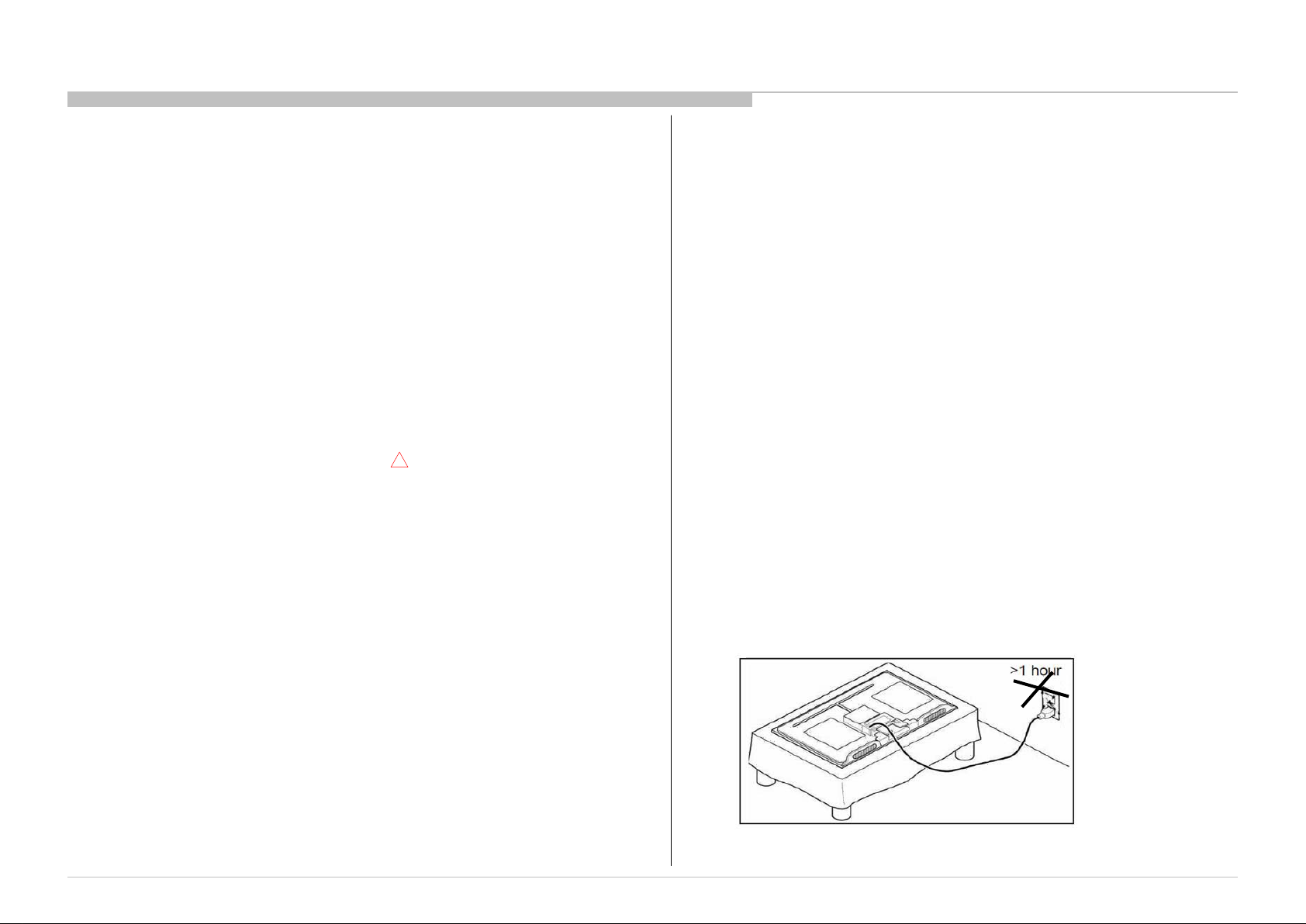
10) Dur i ng the r epai r , D O NO T l eav e the Pow er On or Burn-in period for more
than 1 hour w hil e the T V i s face dow n on a c l oth.
Figure 1. TV is faced down on a cloth during repair.
5
Page 6

1-3. Caution About the Lithium Battery
1) Danger of explosion if battery is incorrectl y replaced. Replace only with
the same or equivalent type.
2) Outer case broken battery shoul d not contact to water.
1-4. Safety Check-Out
After correcting the original service problem, perform the following
safety checks before releasing the set to the customer:-
1) Check the area of your repair for unsoldered or poorly soldered
connections. Check the entire board surface for solder splashes and bridges.
2) Check the inter board wiring to ensure that no wires are pinched or
contact high-wattage resistors.
3)Check all control knobs, shields, covers, ground straps and mounting
hardware have been replaced. Be absolutely certain you have replaced all
the insulators.
4) Look for unauthorized replacement parts, particularly transistors that
were installed during a previous repair. Point them out to the customer and
recommend their replacement.
5) Look for parts which, though functioning show obvious signs of
deterioration. Point them out to the customer and recommend their
replacement.
6) Check the line cords for cracks and abrasion. Recommend the
replacement of any such line cord to the customer.
7) Check the antenna terminals, metal trim, metalized knobs, screws and all
other exposed metal parts for AC leakage. Check leakage test as described
next.
8. For safety reasons, repairing the Power board and/or Inverter board is
prohibited.
1-5.Leakage T est
(To protect elec tri c shock when custom er touch the ter minal .)
Leakage curr ent can be measured by V: Voltmeter or oscilloscope (r.m.s. or
peak reading)
Stabilized pow er supply instrument and isol ated voltage transform er:
Use too much curr ent c apacity and isol ated voltage tr ansformer does not
need to use stabili zed power supply equipm ent.
Specificati on of RM S volt meter: I nput res istanc e > 1 Mohm, I nput
capacitance < 200 pF, Frequency range: 15 Hz – 1MH z . Refer Figure 1.
Isolated ty pe volt -meter (F LUKE 8921A etc *1)
*1 Not use FLUKE 8920A that c onnected to prot ectiv e eart h by diode
# Leakage current of measurement instrument is less than 10μArms when
under test equi pment AC plug is opened
# Set up the following conditi on and tur n on the set. Applied v oltage:
Nominal i nput volt age (Des cri ption on Nam eplate)
# Measur e the leakage cur rent bet ween one phas e conduc tor and neutral
for termi nal 1 and termi nal
2. Read rms value, and then calculate to peak value PEAK VALUE =√2
RMS VALUE
Comply w ith the following requir ement
Class II equipment (2-pin pl ug): for eac h termi nal, the w orst val ue of
measurement m ust not exceed AC 283uA peak).
Note: includi ng AC adaptor, AC adaptor/DC operated unit combi nation
Note: Products which are always used in touch with human body: 141uA
(peak)
Note: As for products destined for Southeast Asia (Rod Antenna is
accessory . Or it is packed with a pr oduc t.) , the worst value must not exceed
AC 141uA (peak).
Figure 1 – Measuring network
for Leakage Current
6
Page 7

1-6. How to Find a Good Earth Ground
1) A cold-water pipe is a guaranteed ear th ground; the cover-plate retaining
screw on most AC outlet boxes i s also at earth ground.
2) If the retaining scr ew is to be used as your earth ground, v erify that i t is at
ground by measuri ng the resistanc e between i t and a c ol d-w ater pipe w ith an
ohmmeter. The readi ng should be zer o ohms.
3) If a cold-water pipe is not accessi ble, connec t a 60- to 100-w att troublelight (not a neon lamp) between the hot side of the recept acle and the
retaining scr ew. Tr y both slots, if necess ary, to locate the hot s ide on the line;
the l am p shoul d l i ght at normal br il l i ance i f the sc r ew i s at gr ound pot enti al
(see Figur e 3).
Figure 3. Checking for earth
ground.
1-7. Lead Free Information
The circui t boards used i n these model s have been pr ocessed using Lead
Free Solder. The boards ar e identified by the LF logo loc ated clos e to the
board designation.
1-8. Handling the FLEXIBLE FLAT CABLE (FFC)
When you insert / pull out FFC, please grasp a reinforcement board and main
body of FFC.
The servic ing of these boar ds r equires special precautions. It is strongly
recommended to use Lead Free Solder m ateri al in order to guarantee optim al
Figure 4: LF Logo
Figure 5: LF logo on circuit board
quality of new solder joi nts.
7
Page 8

1-8. Handling the FLEXIBLE FLAT CABLE (FFC) ( continue )
<INSERTION>
Insert pr operl y wit hout slanti ng
<PULL OUT>
Press rel ease button at the sam e
time pull out FFC cable
8
Page 9

1-8. Handling the FLEXIBLE FLAT CABLE (FFC) ( continue )
9
Page 10

1-8. Handling the FLEXIBLE FLAT CABLE (FFC) ( continue )
10
Page 11

1-9. Solder-less tuner replacement procedure
① The insertion & extraction angle of the module is permitted to
specified degree for connec tor
For removing Tuner Module,
In the case of small type Tuner module.
After un screwed, Automatically the Module
will float to co rrect degree.
So please extract it with keeping this degree.
θ≒20°
Service manual operation (agreed by service member):
Not using insertion jig. Due quantity not many as production.
SC can control by:
1) Issue service manual for WW ASC.
2) Give training/lecture how to assemble tuner. Will be handle by SOEM
service
Push down to screw.
20°
Please c o nfirms whether no dust and no bend on
terminal of connecter(CN2800) and card-edge
connecter
Attachm e nt order of screw.
1. Side of antenna ter minal (W/BFX board).
2. Rear side of Tuner module.
1
2
11
Page 12

1-9. Solder-less tuner replacement procedure (Cont. )
12
Page 13

1-9. Solder-less tuner replacement procedure ( Cont. )
13
Page 14
SECTION 2
SELF DIAGNOSTIC FUNCTION
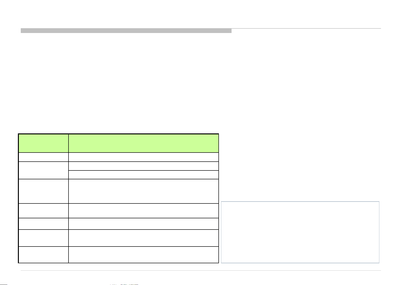
The units in this ma nual conta i n a self-diagnostic function. If an error occurs, the Smart Co re Red LED will automatic ally begin t o flash.
The number of times the LE D flashes t ra nslates to a pr obab l e sour c e of the p roblem.
A definiti on of t he Smart Co re Red LE D fla s h indica t or s is list ed in t he ins truc ti on manu a l for the us er ’s knowled g e a nd r efer enc e.
If an error symptom ca nnot b e r epr odu ced, the r emote c omman d er ca n be us ed t o review t he f a ilu r e occur rence da t a stored in memory to reveal past problems and how
often thes e p r ob lems oc cu r .
DIAGNOSTIC TEST INDICATORS
When an error occurs, the Smart Co re Red LED will f lash a set nu mber of ti mes to indi c ate the possi ble cause of the pr oblem.
If ther e is more than one er ror , the LED will identify the f irst of the p roblem a reas .
Result for all of the following diagnostic items are displayed on screen.
If the scr een dis p la ys a “0”, no error has occu r r ed .
Smart Core RED
LED blinking count
2x
3x
4x
(KP/KPSP/KS
only )
5x
6x <G/P/B/LD> Backlight failure [BACKLIGHT]
7x
8x (KP/KPSP)
8x (KS)
Detection Items
<B/G/A/LD> Main 12V over voltage [MAIN_POWER]
<B> Main 5.0V failure [DC_ALERT]
<B/S/K> Audio amp. protection [AUD_ERR]
<LD/P> LED driver failure/LED voltage protection [LD_ERR]
<LD/P>Error detection of the I2C communication between the
Main device and the LD IC.[BCM_ERR]
<P/T/G/B> Panel ID EEPROM I2C No ACK (Also panel power
failure is a suspect) [P_ID_ERR]
Over temperature protection [TEMP_ERR]
<B> Temp. sensor I2C No ACK [TEMP_ERR]
<B> 4KBE Error (4KBE WDT)
<B> 4KPQ Error (4KPQ WDT)
Blue italic: detect at startup sequence only.
<G>: Power supply board,
<B>: Main board,
<T>: T-con board,
<LD>: LD board
<P>: Panel module,
<S>: Speaker,
<A>: Power Adapter,
<Tu>: Tuner board,
<K> : Audio board (KFW/KPSP only)
(if AC adapter model, it would power supply for Set),
14
Page 15
Record Only
Item
TU_DEMOD
TCON ERR
(KP/KPSP/KS/KH only )
FRCTC_I2C
(KS/KH)
(KF/KFW/KFC)
Detection Items
<B/Tu> Tuner & Demodulator I2C communication failure
Tuner board set detect signal monitoring
<T> T-CON device I2C communication failure
<B> FRC device is not finished Initial sequence
FRC device I2C communication failure
<T/B> FRC device is not finished Initial sequence
FRC device I2C communication failure
Blue italic: detect at startup sequence only.
<G>: Power supply board,
<B>: Main board,
<T>: T-con board,
<LD>: LD board
(if AC adapter model, it would power supply for Set),
<P>: Panel module,
<S>: Speaker,
<A>: Power Adapter,
<Tu>: Tuner board,
<K> : Audio board (KFW/KPSP only)
AUD_ERR_I2C
(KP/KPSP/KS/KH only )
<B/K> Audio amp I2C communication failure
4KPQ_ERR_I2C
(KS/KH only)
<B> 4KPQ d e vice I 2C communicatio n failure
LED Pattern
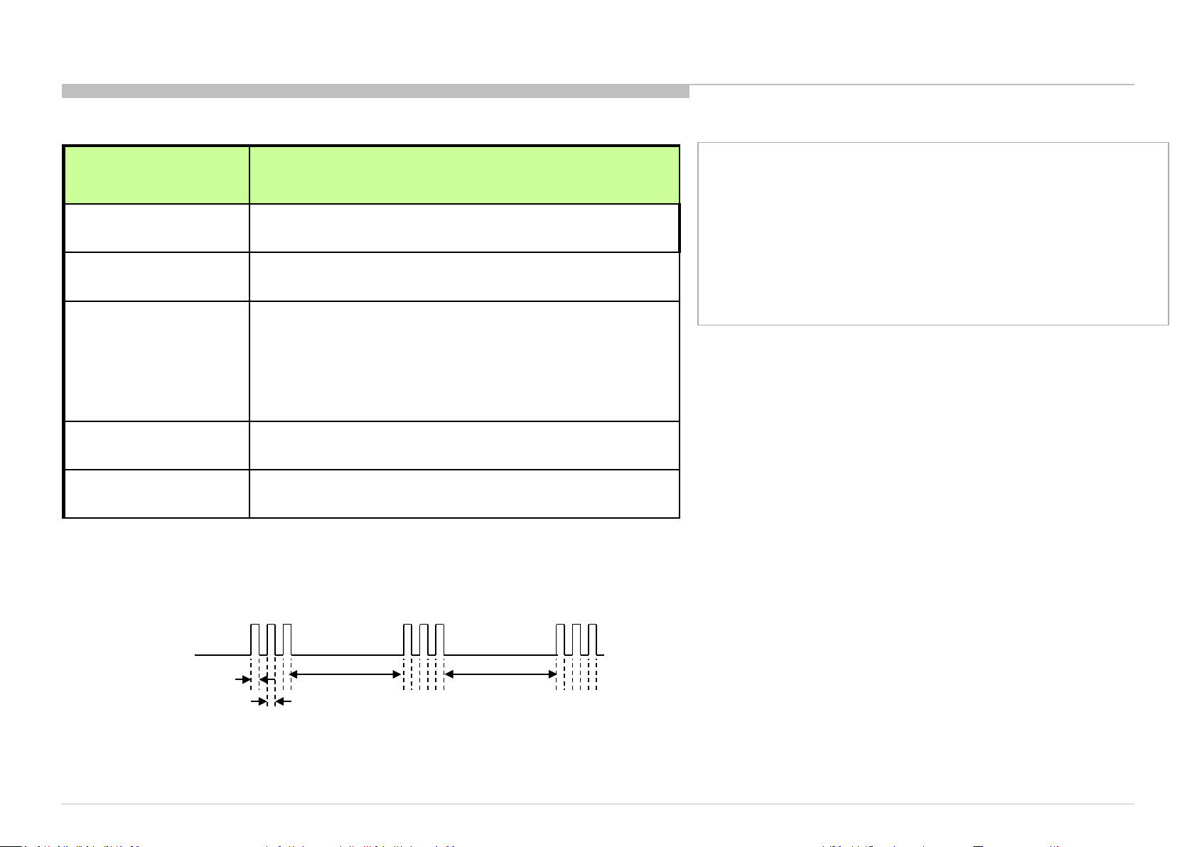
When safety shutdown occurs, Standby LED display reports the cause by using the lightning patterns as indicated below.
0.5sec
Example: The figure above shows LED display when SHUTDOW N is caused by Audio Error.
It repeats f lashing f or a specified number of times in 0.5s ec/cycl e and has a 3 seconds interval of lighting off.
Please note th at a 3 sec onds int erv al of light ing off is fixed regar dl ess of abnor m al s tate typ es.
0.5sec
3.0sec 3.0sec
15
Page 16

Entry (Self Diagnosis Display)
- Go to the standby by a remote.
- Push the buttons sequentially:
<Display><5><Vol-><Power>
Exit
-If you want to finish service mode app, do AC OFF/ON
→*Service mode app is disable perfectly
-if you want to move home menu, push <HOME>button
→*Service mode app do background(not disable
perfectly)
Format of error timestamps
YYMMDDhhmmss (in UTC)
Example:
120823132523 -> Aug 23 2012 13:25:23 UTC
* Only when time is set, an error timestamp
is saved.
Smart
Core Red
LED
blinking
count
Error Item
SELF CHECK
Back
<<
002 MAIN POWER 000000000000 000000000000 000000000000 000
003 DC ALERT 000000000000 000000000000 000000000000 000
003 AUD ERR 150101000018 150101000018 150101000018 003
003 AUD ERR I2C 150101000123 150101000045 150101000045 003
003 TU DEMOD 150101000218 150101000223 150101000105 003
004 LD ERR 000000000000 000000000000 000000000000 000
004 BCM ERR 000000000000 000000000000 000000000000 000
005 TCON ERR 150101000504 000000000000 000000000000 001
005 P ID ERR 000000000000 000000000000 000000000000 000
006 BACKLIGHT ERR 000000000000 000000000000 000000000000 000
007 TEMP ERR 150101000200 150101000002 000000000000 002
008 4KBE ERR 000000000000 000000000000 000000000000 000
00005 00414 00002
[Home]Exit
Error
timestamp
for last
recorded
error
Error
timestamp
for second
last
recorded
error
Error count
Error
timestamp
for 3rd
last
recorded
error
Panel Operation Time clear
<7> -> <0>
Timestamps and Error Count clear
<8> -> <0>
Tot al Operation Time and Boot Count clear
<9> -> <0>
Total Operation Time [hr] – Boot Count – Panel Operation Time [hr]
•Panel Operation Time is recorded every 30 min, but Tot al
Operation Time is recorded every 1 hr.
Therefore, the panel op. time might become larger than the
total op. time.
16
Page 17

Triage C hart
Remote
Bluetooth
No White Po wer
LED & does not
colored
lines or
dots
One of
Smart Core
(Set is still
Bluetooth /
(OSR) can't
Before you make t he service cal l…
1. Confirm the symptom from the customer.
2. Select that sympto m fro m the chart.
3. Bring a ll the b o a r d s and ca b les liste d for that symp to m.
4. Follow the troub lesho oting c harts in the technical guid es to isolate the boar d.
5. Chart
Color Code
RED DOT: Mo st likely defective pa r t
BLUE TRIANGLE: Secondary possible defective part
ABC BLACK TEXT: Board that may correct the symptom
Symptoms - Shutdown. Power LED
blinking red diagnostics sequences
Reference
2 3 4 5 6 7 8 9 10
B* Board
Power
reponse to
remote (Dead
Set)
No
Video
- mi ssing or
distorted
Station
ary
video
Inputs
No
No
video
all
Inputs
No
Remote
Networ
k
Wireless
can't
connect
Audio
No
Audio
Smart
Core
no LED
alive)
GN3 KF segment
(BT)
One Step
Remote
connect
G* Board
H* Board
K* Board
Speaker
Wifi & BT
Module
LD* Board
V By One
FFC
Tcon
LCD Panel
17
Page 18

SECTION 3
TROUBLESHOOTING
KF/KFW 55” No Power(GL71 PS U board)
Switch Off plug(AC Off)
NO POWER
Check
Fuse F6101,
Open?
Open T V rear c ov er to check PS U Boar d
Wait more than 5 minutes before start
This is to ensure PSU is not in protection mode
PSU broken*
Yes
Replace PSU
Connector CN6401
Check
BL_ON
PIN 7
No Voltage
Main Board Pr oblem
AC Off
AC ON
Connector CN6401
Connector CN6401
Connector CN6401
no
Check
STBY3.3V
PIN 5
Okay
Check
POWER_ON
PIN 9
Okay
Check
REG12V
PIN 13to18
Okay
No Voltage
No Voltage
No Voltage
PSU broken*
Replace PSU
Main Board Pr oblem
PSU broken*
Replace PSU
Okay
Check +Out2
and +Out3 at
CN6801
Okay
PSU OK
Connector
No Voltage
Output
Name
PSU broken*
Replace PSU
Input/output
Voltage
CN6401 STBY3.3V 3.35~3.55V 5
CN6401
POWER_
ON
2.6~3.55V 9
CN6401 REG12V 12.2~13.2V 13~18
CN6401 BL_ON 2.6~3.55V 7
CN6801 +OUT2/3 85.5~125.3V 2~3
*If PSU board replaced, pl ease proceed with PSU
standalone check
PIN
TV Business Division
18
18
Page 19

GL71 Brok en PSU standalone checking
1. Appearance check
2. PS U info checking and confirmation
3. Broken parts checking
Note: PSU board C AN NOT be repair(unless requested by design)
Any request to repair will be instruct.
TV Business Division
19
19
Page 20

Appearance check
No Operation Tool Remarks
1 Check A-side appearance Glove Visual check
Keep record PC/Pen/Photo
2 Check B-side appearance Glove Visual check
Keep record PC/Pen/Photo
1 2
Criteria: No abnormality
Exam ple: PWB crack/Burn mark
PWB crack
A-side
TV Business Division
B-side
Burn mark at AC inlet PIN(L~N)
20
20
Page 21
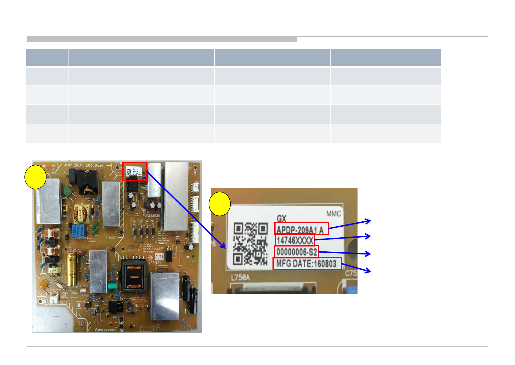
PSU info checking and confirmation
No. Operation Tool Remarks
1 Check label marking Glove Visual check
Keep record PC/Pen/Photo
2 Record PN/SN/MFG Date Glove Visual check
Keep record PC/Pen/Photo
1
2
TV Business Division
PSU name
PSU PN(Part Number)
PSU SN(Serial Number)
MFG Date(Manufacturing date)
21
21
Page 22

Broken parts checking
No. Parts Checking Criteria
1 F6101(Fuse) Resistance NG (high impedance)
2 C800A(main cap) Visual NG (vent)
3 BD1(Bridge di ode) Resistance NG (low impedance)
4 Q800A(PFC MOSFET) Resistance NG (low impedance)
5 D800A(PFC diode) Resistance NG (low impedance)
6 Q600(LLC MOSFET) Resistance NG (low impedance)
7 Q601(LLC MOSFET) Resistance NG (low impedance)
8 D120A(LLC Rectifier for 12V) Resistance NG (low impedance)
9 D120B(LLC Rectifier for 12V) Resistance NG (low impedance)
10 Q750A(LED boost MOSFET) Resistance NG (low impedance)
11 D751A(LED boost diode) Resistance NG (low impedance)
12 D 750(LLC Rectifier for LED) Resistance NG (low impedance)
13 D 751(LLC Rectifier for LED) Resistance NG (low impedance)
14 D 752(LLC Rectifier for LED) Resistance NG (low impedance)
15 D 753(LLC Rectifier for LED) Resistance NG (low impedance)
16 R915(Aux Fusible resistor) Resistance NG (high impedance)
17 D950A(Aux Rectifier diode) Resistance NG (low impedance)
18 Q 123( Tcon12V switch M O SFE T) Resistance NG (low impedance)
TV Business Division
22
22
Page 23

Broken parts checking(parts location)
Q750A
BD1
F6101
C800A
D800A
R915
Q600
Q601
Q800A
D751A
D751
D750
D753
D752
Q123
D120A
D120B
D950A
23
23
Page 24

Escalation Check sheet(Hardware)
Defect symptom Details
Does problem occur during first turn on?
Frequency of the symptom
Does the symptom recover by AC Off for more than 5
minutes?
Please describe the recover method
Please provide the humidity and temperature
condition of the defect area/ Wheater During
Problem Occur
Symptom occur for 1 particular set?
Able to duplicate the symptom in workshop
Other comment/Information
Any LED blink indication
Are there any other equipment or devices broken
together?
Is there any burn mark could be notice on the
defective board?
Symptom occur on all input modes
(HDMI, Video, Analogue RF, Digital RF)
Any other devices connected to TV set
If yes, please provide the device and brand
Yes: No:
Always: Intermittently:
(if any)
Yes: No:
Yes: No:
Yes: ____times No:
Yes: No:
Yes: No:
Temperature:
Yes: No:
Yes: ____parts No:
Yes: No:
____⁰C Humidity: ____H
(Specify)
(Specify)
TV Business Division
24
24
Page 25

1.1 No power - LD board
START
LD board
1. Check fuse impedance
F1001
Is < 1ohm?
yes
2. Check impedance
D1001 to GND
Is > 1kohm?
yes
3. Check MOSFET
Q1007
Is > 1kohm?
yes
4. Check MOSFET
Q1002
Is > 1kohm?
yes
5. Check MOSFET
Q1008
no
no
no
no
no
Fuse F1001 broken
Diode D1001 broken
MOSFET Q1007 Broken
MOSFET Q1002 Broken
MOSFET Q1008 Broken
2
Q1007
4
1
F1001
D1001
3
Q1002
5
Is > 1kohm?
yes
Check B board
TV Business Division
Q1008
25
25
Page 26

1.1 No power - LD board
12V DDCON check
START
Check fuse F1000
Is < 1ohm
yes
Check Input to GND
Is > 1k ohm?
yes
Check Input to Output
Is > 1k ohm?
yes
Check Output to GND
Is > 1k ohm?
yes
Check 12V
C1016 voltage
Is voltage <12V?
yes
Check EN POWER_ON
R1003 voltage
Is voltage >2.5V?
yes
Check Vcc
C1009 voltage
Is voltage >5.0V?
no
no
no
no
no
no
≥ 12V
Fuse F1000 broken
DDC IC1000 broken
DDC IC1000 broken
DDC IC1000 broken
Check B-Board
Troubleshooting flow 1.2
IC1000 broken
12V_TCON check
yes
Check 12.5V_TCON
Is voltage > 12.0V?
Check TCON_ON
Is voltage > 3.0V?
Check MOSFET
no
no
C1024
yes
no
Q1006
Is > 1kohm?
yes
12V power OK
Check other troubleshooting flow
END
Main device failure
Q1006 broken
yes
Check point on PWB refer next slide
26
26
Page 27

1.1 No power - LD board
Input to GND
Impedance check
F1000
C102
4
+12.5V_TCO
N
Q1006
Input to Output
Impedance check
TV Business Division
C1016
R1003
C1009
Impedance check
Output to GND
Impedance check
27
27
Page 28

1.2 No Power u-com Failure
BFX Board
G-Board or LD
G-Board or LD
or IC409
+3.3V_STBY
POWER_ON
BL_ON
P-on u-com control signal path summary
#pin1
Vdd Ucom
supply voltage
#pin18
IC401
#pin19
B-Board
#pin2
#pin12
#pin5
#pin10
#pin16
#pin11
#pin9
P-on u-com
#pin13
#pin14
OPWRSB
ORESETB
AC_OFF_INFO
PANEL_PWR_ON
X_SYSTEM_RST
P_ON_VBUS
PGOOD_1
P_ON_#1
P_ON_#2
SOC Muffin 2 (IC1000)
Tuner (CN2800)
DDC: +5.0V_VBUS (IC402)
DDC : +1.0V_M2 (IC604)
DDCs : +1.8V_TU (IC405)
DDCs : +5V_MAIN (IC404), +3.3V_MAIN
(Q406/Q407)
LDOs: +1.05V_M2_A_1 (IC603),
+12V_REG
R430
R437
GND
#pin7
MAIN_VCC
ADC port
#pin3
#pin15
#pin8
+1.05V_M2_A_2 (IC606), VCC3IO_EMMC
(IC2002)
DC_OFF_DET
DC_OFF_DET (IC400)
P_ON_LNB
+12V_LNB (Q408/Q409)
BL_MUTE
SOC Muffin 2 (IC1000)
28
Page 29

1.2 No Power u-com Failure
START
Check VDD
C419 Voltage.
Is the voltage >3.0V?
yes
Check DC_OFF_DET
C504 Voltage.
Is the voltage >3.0V?
yes
Check OPWRSB
R441 Voltage.
Is the voltage 0V?
yes
no
no
no
BFX Board
Check +3.3V_STBY
C413, CN400 #24pin
Check DC_OFF_DET
IC400
SOC
Muffin 2
problem
Check MAIN_VCC
R437 Voltage.
Is the voltage >1.6V?
yes
Check P_ON_VBUS
P-on ucom #pin11
is >3.0V?
yes
Check P_ON_#1
P-on ucom #pin13
is >3.0V?
yes
no
no
no
Check +12V_MAIN Line
(G board, LD).
Change IC401
Change IC401
Check POWER_ON
P-on ucom #pin19
Is the voltage >3.0V?
yes
Check P_ON_LNB
P-on ucom #pin15
Is the voltage >3.0V?
yes
no
no
Try AC Off and On after few minutes.
If #pin19 keep Low, change IC401.
If #pin19 goes High few seconds and downs to Low,
Check +12V_MAIN Line (G board, LD).
Change IC401
Check PGOOD_1
R434 Voltage.
Is the voltage >3.0V?
Continue next page…
no
1.3 No POWER - DDCON/LDO
Check 1.0V DDCON (IC604)
29
29
Page 30
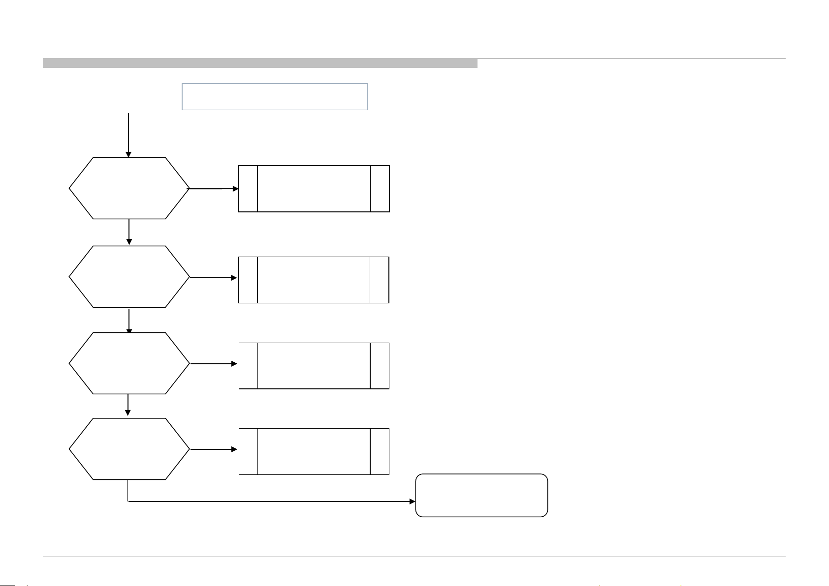
1.2 No Power u-com Failure
BFX Board
Cont…
yes
Check P_ON_#2
P-on ucom #pin14
Is the voltage >3.0V?
yes
Check ORESETB
P-on ucom #pin12
Is the voltage >3.0V?
yes
no
Change IC401
no
Change IC401
Check X_SYSTEM_RST
P-on ucom #pin16
Is the voltage >3.0V?
yes
If BL_MUTE (R435) is 0V
Check BL_ON
P-on ucom #pin18
Is the voltage >3.0V?
yes
no
no
Change IC401
Change IC401
END
Ucom IC401 is working OK
30
30
Page 31
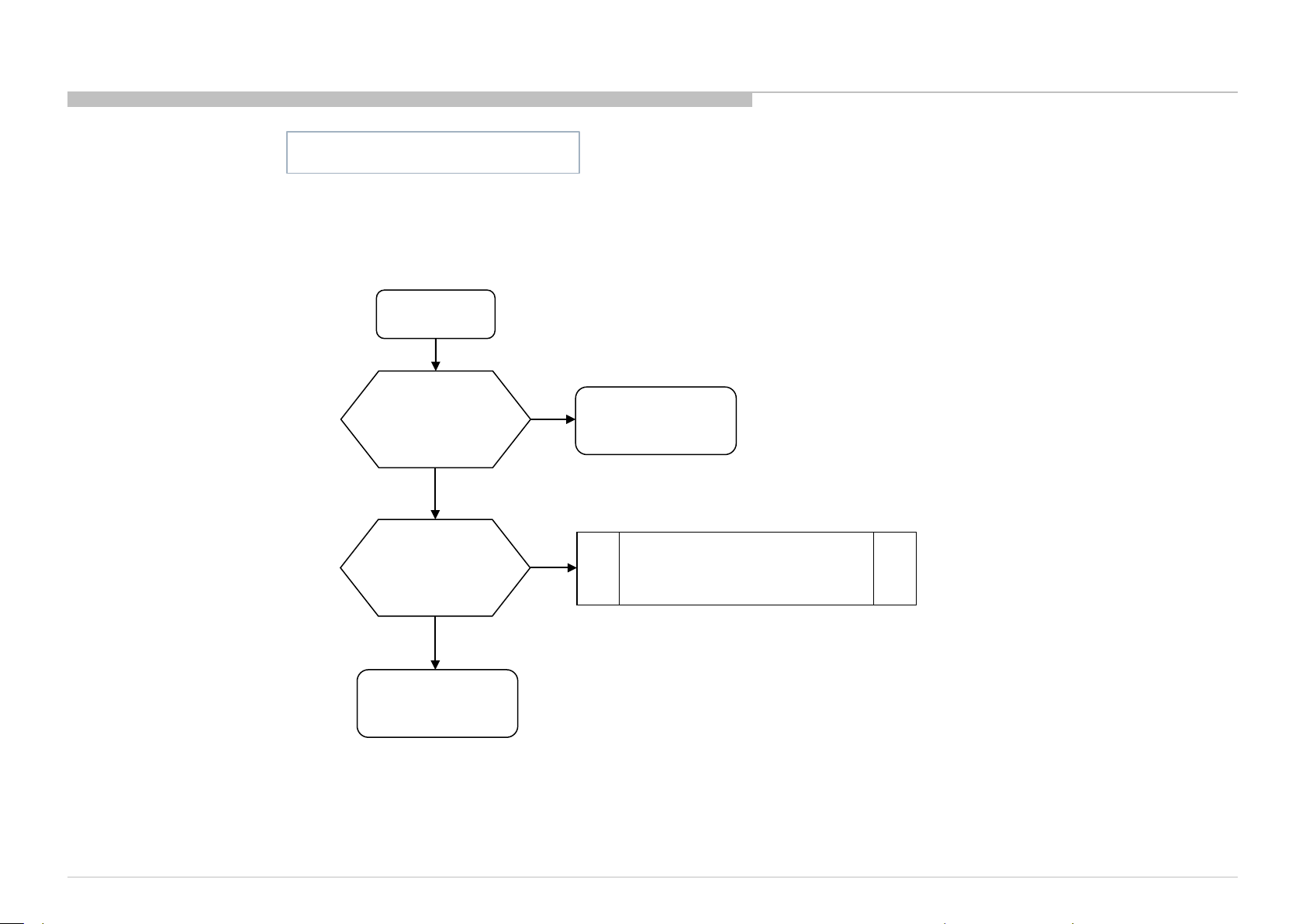
1.2 No Power u-com Failure
BFX Board
DC_OFF_DET check
START
Check DC_OFF_DET
R420
Is voltage < 3V?
yes
Check Vdd
C418
Is voltage < 5V?
yes
END
IC400 is working OK
no
END
IC400 is working OK
no
Change IC400
31
31
Page 32
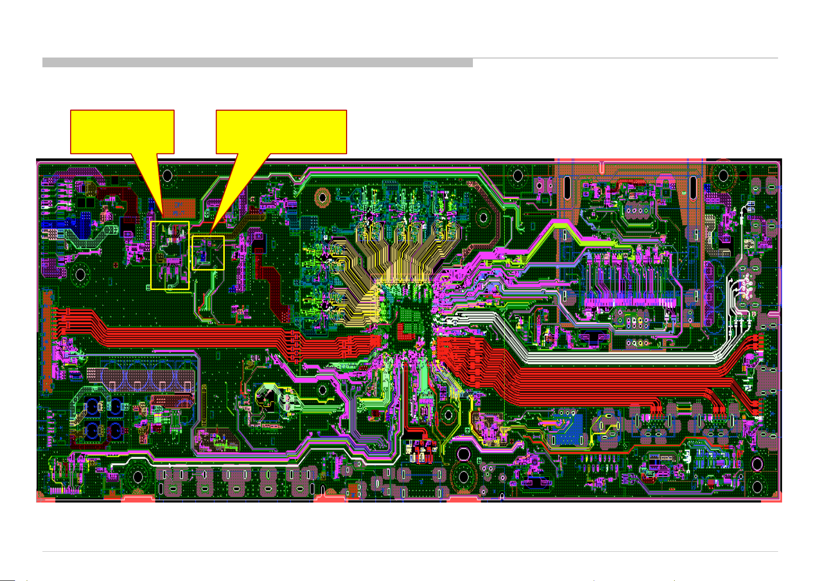
1.2 No Power u-com Failure
P-on u-com & DC_OFF_DET Location
(IC401)
P_ON_U-
Com
(IC400)
DC_OFF_DET
32
32
Page 33
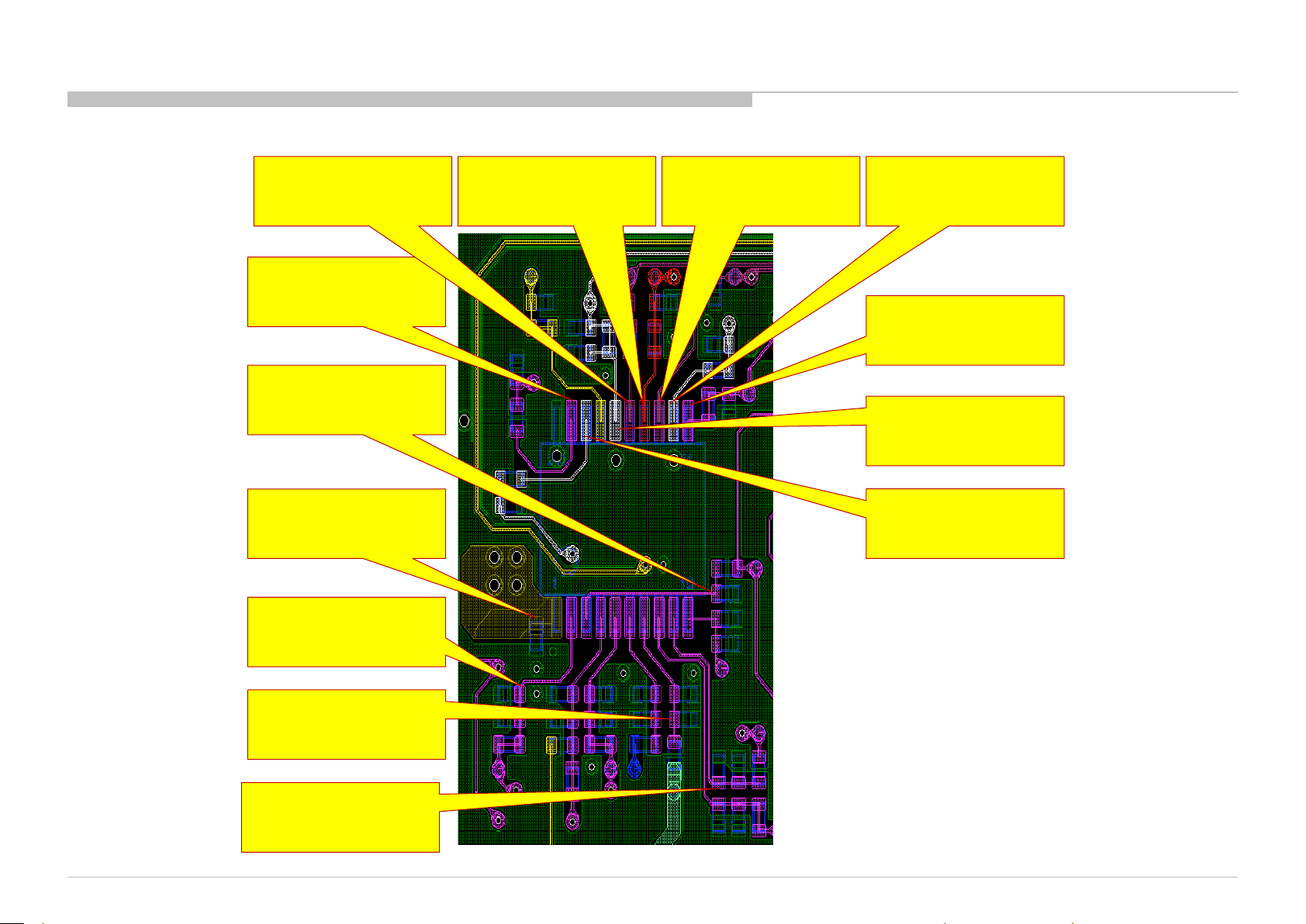
1.2 No Power u-com Failure
1.2 No Power u-com Failure
P-on u-com & DC_OFF_DET Location
5. P_ON_LNB
> 3.0V
4. POWER_ON
> 3.0V
2. C504 > 3.0V
1. C419 > 3.0V
10. P_ON_#2
> 3.0V
IC401
8. P_ON_#1 >
3.0V
11. ORESETB
> 3.0V
7. P_ON_VBUS
> 3.0V
12.
X_SYSTEM_RS
T > 3.0V
13. BL_ON >
3.0V
3. R411 > 3.0V
6. R437 > 1.6V
9. R434 > 3.0V
33
33
Page 34
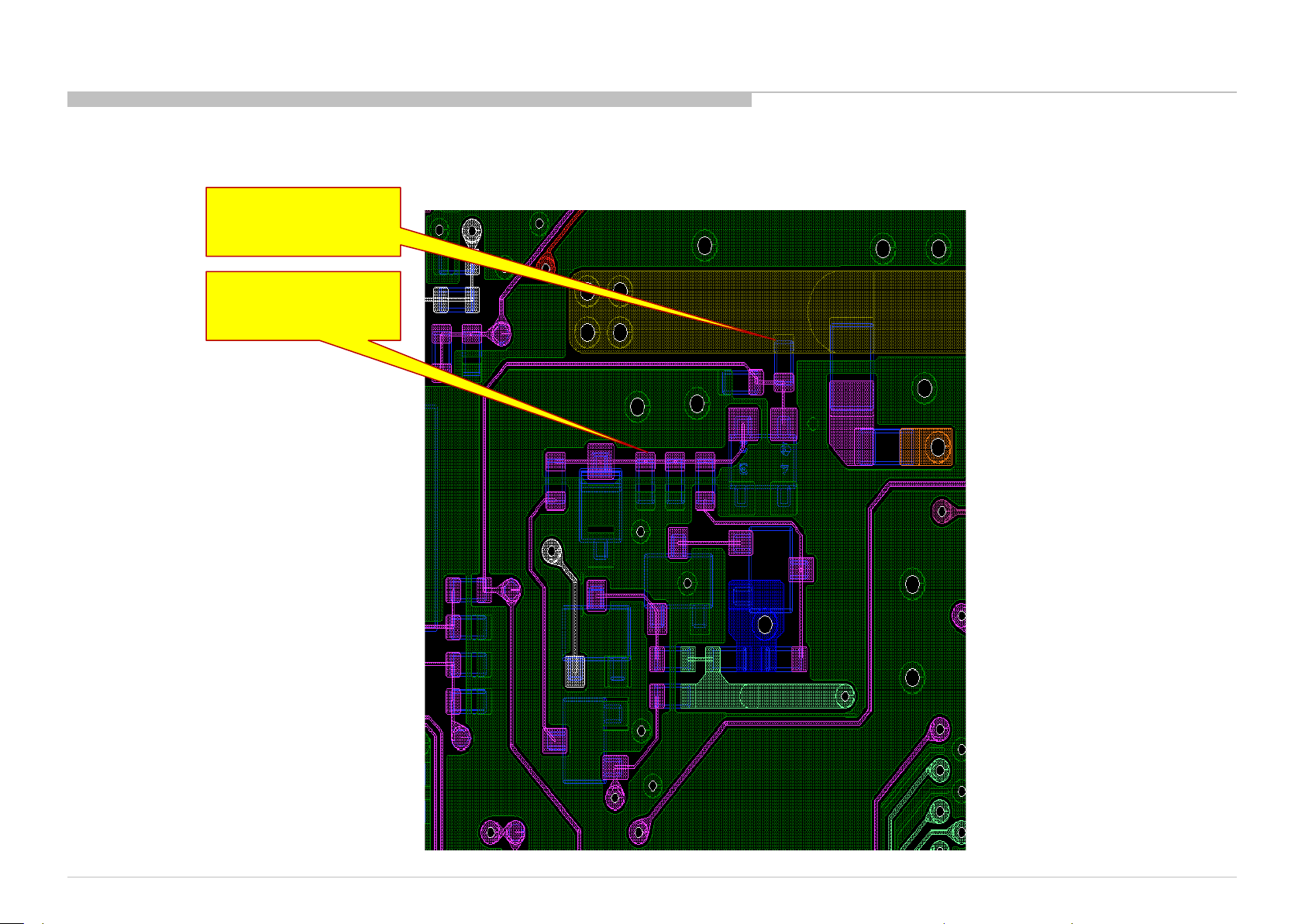
1.2 No Power u-com Failure
1.2 No Power u-com Failure
DC_OFF_DET component location
1. R420 >
3.0V
2. C418 >
5.0V
IC400
34
34
Page 35
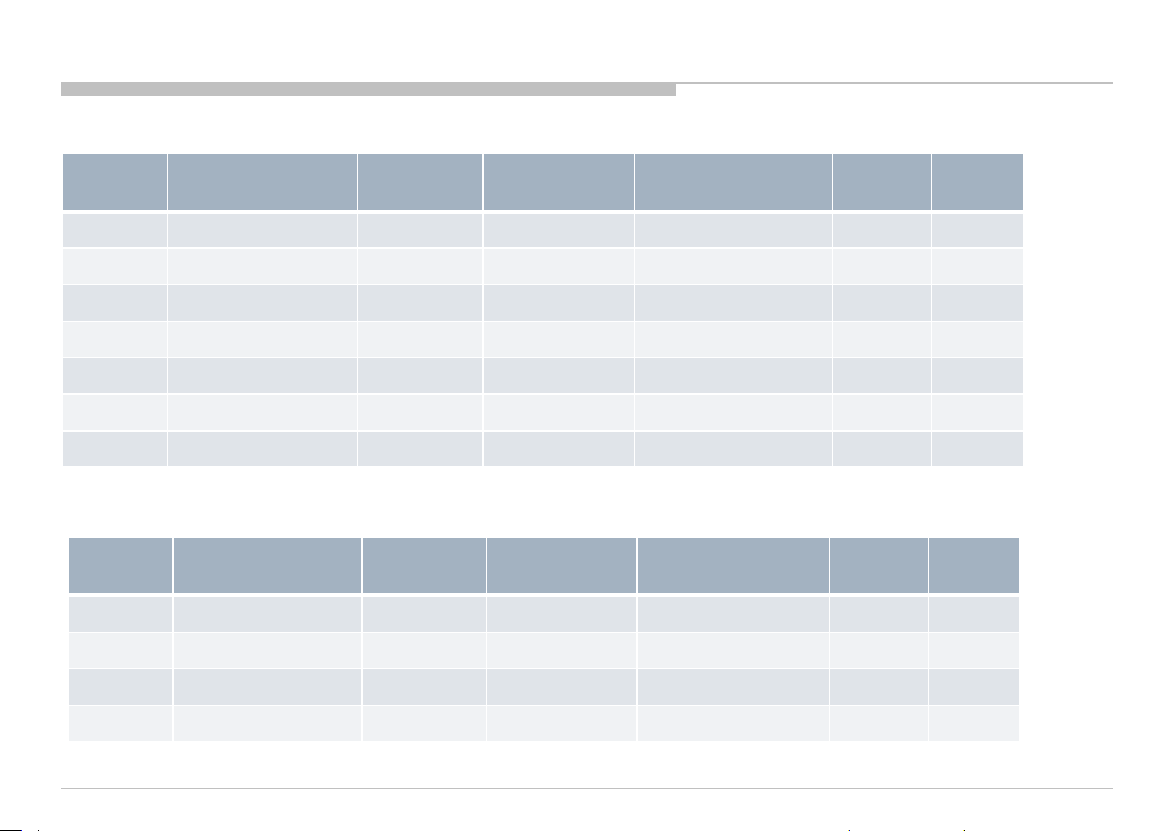
1.3 No Po wer DDC ON/L DO
DC-DC Converter Reference Points
IC Ref Voltage supply
IC403 +3.3V_STBY C447 R467
IC601 +1.5V_DDR C609 C605 +5V_STBY - IC404 +5.0V_MAIN C456 R480 P-on ucom IC401 F402 IC402 +5.0V_VBUS C431 R455 P-on ucom IC401 F400 C428
IC604 +1.0V_M2 C629 R623 P-on ucom IC401 F600 C623
IC405 +1.8V_TU C464 IC405 #pin4 P-on ucom IC401 F403 -
Q407 3.3V_MAIN Q407 #pin2 Q407 #pin1 P-on ucom IC401 - -
Output
ref.
Enable pin Enable source Fuse
+19.5V_12.5V_MAIN
F401 C443
Vcc
ref.
LDO Reference Points
IC Ref Voltage supply
Output
ref.
Enable Pin Enable source Fuse
VDD
ref.
IC602 +1.05V_M2_STBY C611 IC602 pin#3 +3.3V_STBY - C610
IC605 +1.05V_M2_ST_ET C631 IC605 pin#3 P-on ucom IC401 - C630
IC603 +1.05V_M2_A_1 C613 IC603 pin#3 P-on ucom IC401 - R612
IC606 +1.05V_M2_A_2 C633 IC606 pin#3 P-on ucom IC401 - R632
35
Page 36
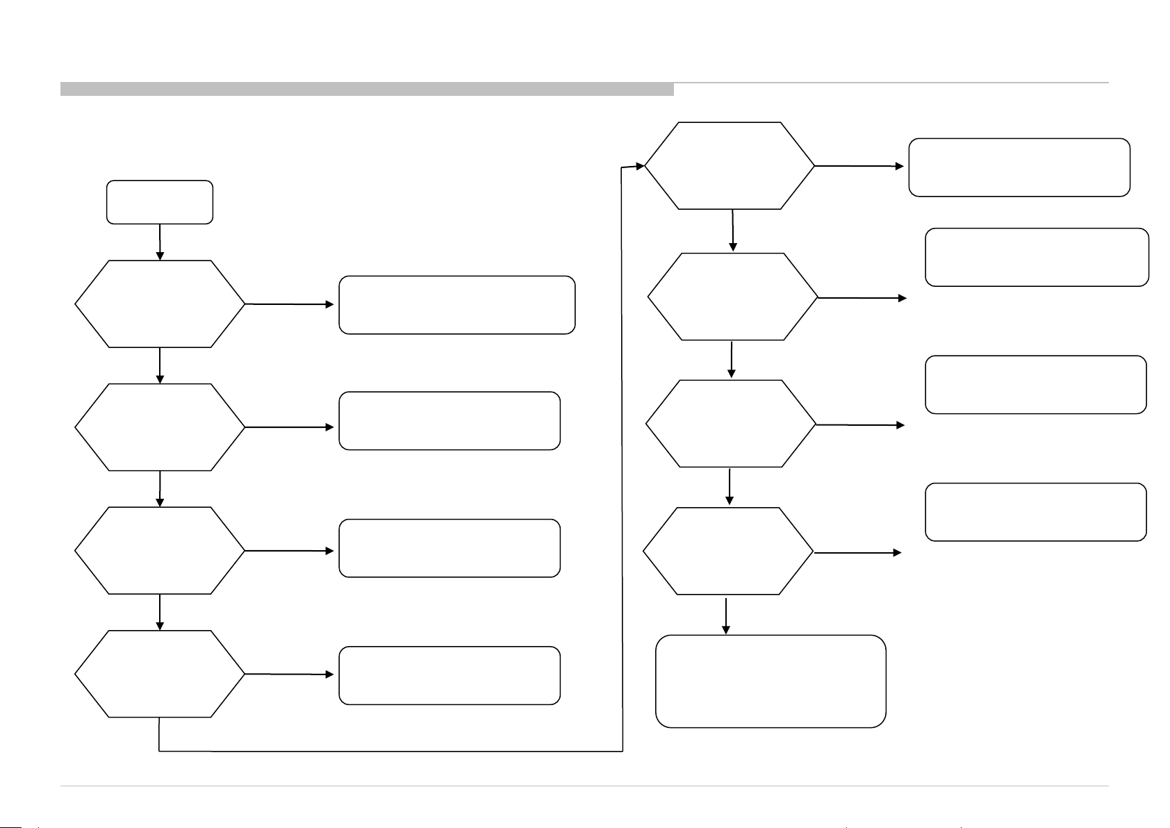
1.3 No Po wer DDC ON/L DO
DC-DC Converter Ov erall C heck
START
Check C447 Voltage.
Is the voltage 3.3V?
yes
Check C609 Voltage.
Is the voltage 1.5V?
yes
Check C456 Voltage.
Is the voltage 5V?
no
no
no
DDC: +3.3V_DDC_OUT check
DDC: +1.5V_DDR check
DDC: +5.0V_M AI N check
Check C629 Voltage.
Is the voltage 1V?
yes
Check C611,
C631, C613,
C633 is it
1.05V?
yes
Check C464 is it
1.8V?
yes
Check 3.3V_MAIN
C612 Voltage.
Is the voltage 3.3V?
no
DDC: +1.0V_M2 c heck
LDO: +1.05V_M 2_xx check
no
DDC: +1.8V_TU check
no
SW: +3.3V_MAIN check
no
yes
Check C431 Voltage.
Is the voltage 5V?
yes
no
DDC: +5V_VBUS check
yes
END
DDCON/LDO working normal
36
Page 37
1.3 No Power DDCON/LDO
1.3 No Po wer DDC ON/L DO
DDC: +3.3V_DDC_OUT check
LD-Board model
Check input
F401 voltage
Is voltage >19.0V?
yes
START
Check fuse
F401
Is fuse OK?
yes
Check EN signal
R467 voltage
yes
no
yes
no
G-Board model
Check input
F401 voltage
Is voltage >12.0V?
no
Change F401
no
G-Board/LD-Board
Is voltage >2.5V?
yes
Check Vcc
C443 voltage
Is voltage >5.0V?
yes
END
no
Change IC403
KF/KFW 55”=G -Board model (PSU)
KF/KFW 43”/49” =LD -Board model (ADP)
37
Page 38
1.3 No Power DDCON/LDO
1.3 No Po wer DDC ON/L DO
DDC: +1.5V_DDR check
START
Check IC404Vcc voltage
Is voltage >12V?
Check Vcc voltage
Is voltage >4V?
no
Is IC600 mounted?
Check Enable
IC600 #pin1
C454
C602
yes
yes
yes
no
no
no
Check Vcc voltage
C602
Is voltage >3V?
yes
Check
D601
Is diode alive?
yes
Change IC600
no
no
Check
D600
Is diode alive?
yes
Change D601
Check +5V_MAIN DDCON (IC404)
no
Change D600
Check +3.3V_STBY.
G board or IC403
Is voltage >2.5V?
yes
Change DDCON
IC601
38
Page 39
1.3 No P owe r DDCO N/LDO
DDC: +5V_MAIN check
START
Check fuse
F402
Is fuse OK?
yes
Check input
F402 voltage
Is voltage >12V?
yes
Check EN signal
R487 voltage
Is voltage >2.5V?
yes
Change IC405
no
Change F402
no
G-Board/LD-Board
no
1.2 N o Power U -Com Failure
39
Page 40
1.3 No Po wer DDC ON/L DO
DDC: +5.0V_VBU S check
START
Check fuse
F400
Is fuse OK?
LD-Board model G-Board model
Check input
F400 voltage
Is voltage >19.0V?
yes
yes
Check EN signal
R455 voltage
Is voltage >2.5V?
Check Vcc
C428 voltage
no
yes
Is voltage >12.0V?
yes
yes
no
Check input
F400 voltage
no
no
1.2 N o Power U -Com Failure
no
Change F400
G-Board/LD-Board
Change IC402
Is voltage >5.0V?
yes
END
KF/KFW 55”=G -Board model (PSU)
KF/KFW 43”/49” =LD -Board model (ADP)
40
Page 41
1.3 No Po wer DDC ON/L DO
1.3 No Po wer DDC ON/L DO
DDC: +1.0V_M2 check
START
LD-Board model
Check input
F600 voltage
Is voltage >19.0V?
yes
Check fuse
F600
Is fuse OK?
yes
Check EN signal
R623 voltage
Is voltage >2.5V?
Check Vcc
C623 voltage
no
yes
Is voltage >12.0V?
yes
yes
no
Change F600
G-Board model
Check input
F600 voltage
no
G-Board/LD-Board
no
1.2 N o Power U -Com Failure
no
Change IC604
Is voltage >5.0V?
yes
END
KF/KFW 55”=G -Board model (PSU)
KF/KFW 43”/49” =LD -Board model (ADP)
41
Page 42
1.3 No Po wer DDC ON/L DO
1.3 No Po wer DDC ON/L DO
LDO: +1.05V_M2_xx check
+1.05V_M2_STBY
START
yes
Check input
C610 voltage
Is voltage >3.0V?
yes
Check EN signal
IC602 #pin3
Is voltage >2.5V?
yes
Change IC602
no
no
DDC: 3.3V_DDC_OUT check
DDC: 3.3V_DDC_OUT check
+1.05V_M2_STBY_ET
START
yes
Check input
C630 voltage
Is voltage >3.0V?
yes
Check EN signal
IC605 #pin3
Is voltage >2.5V?
yes
Change IC605
no
no
DDC: 3.3V_DDC_OUT check
1.2 N o Power U -Com Failure
42
Page 43
1.3 No Po wer DDC ON/L DO
1.3 No Po wer DDC ON/L DO
LDO: +1.05V_M2_xx check
+1.05V_M2_A_1
START
yes
Check input
C612 voltage
Is voltage >3.0V?
yes
Check EN signal
IC603 #pin3
Is voltage >2.5V?
yes
Change IC603
no
no
SW: 3.3V_MAIN check
1.2 N o Power U -Com Failure
+1.05V_M2_A_2
START
yes
Check input
C632 voltage
Is voltage >3.0V?
yes
Check EN signal
IC606 #pin3
Is voltage >2.5V?
yes
Change IC606
no
SW: 3.3V_MAIN check
no
1.2 N o Power U -Com Failure
43
Page 44
1.3 No Po wer DDC ON/L DO
1.3 No Po wer DDC ON/L DO
DDC: 1.8V_T U check
START
Check fuse
F403
Is fuse OK?
yes
Check input
F403 voltage
Is voltage >12.0V?
yes
Check EN signal
IC405 #pin4
Is voltage >2.5V?
yes
Change IC405
no
Change F403
no
G-Board/LD-Board
no
1.2 No P ower U -Com Failure
44
Page 45
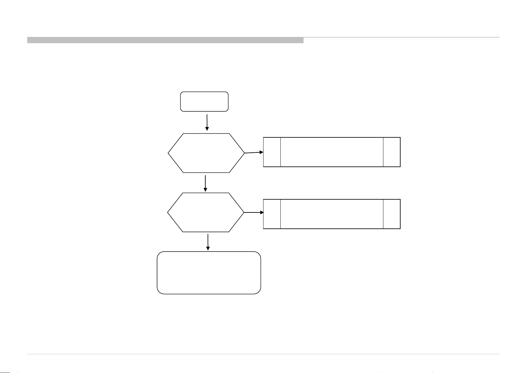
1.3 No Po wer DDC ON/L DO
1.3 No Po wer DDC ON/L DO
SW: +3.3V_MAIN check
START
Check VG signal
Q407 #pin1
Is voltage > 3.0V?
yes
Check VB signal
Q406 #pin1
Is voltage > 3.0V?
no
1.2 N o Power U -Com Failure
no
yes
Change Q407
Change Q406
45
Page 46
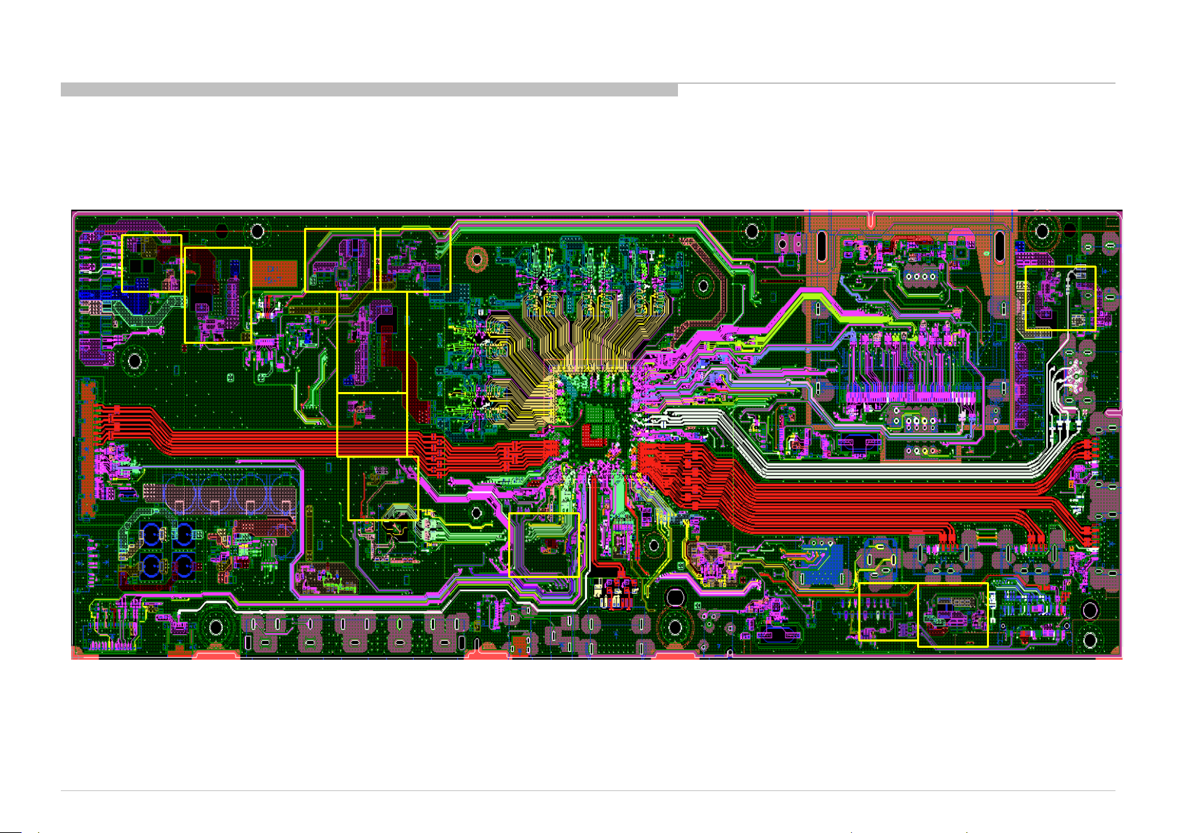
1.3 No Po wer DDC ON/L DO
DDC & LDO Locations
Q40
6Q4
07
IC40
3
IC40
4
IC60
4
IC60
3,
IC60
6
IC60
2
IC60
1
IC60
5
Q40
8
Q40
9
IC40
2
IC40
5
46
Page 47
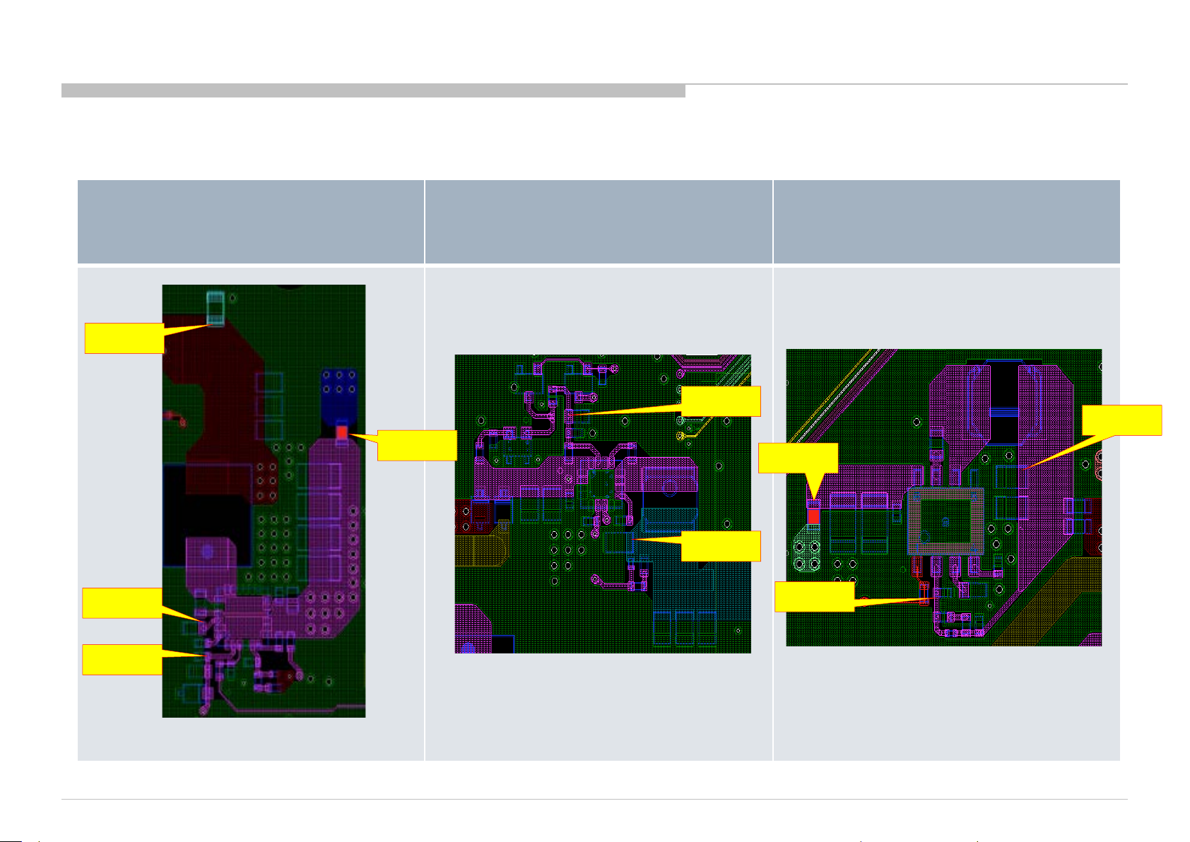
1.3 No Po wer DDC ON/L DO
DDC & LDO Locations
DDC:
+3.3V_DDC_OUT
C447
C443
IC403
DDC: +1.5V_DDR DDC: +5.0V_MAIN
C605
C456
F401
F402
IC601
IC404
C609
R480
R467
47
Page 48
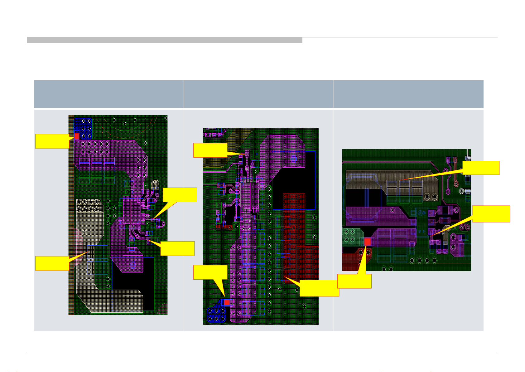
1.3 No P owe r DDCO N/LDO
DDC & LDO Locations
DDC: +5.0V_VBUS DDC: +1.0V_M2 DDC: +1.8V_TU
F400
C623
C464
C431
IC402
R455
C428
F401
IC604
C629
F403
IC405
#PIN4
48
Page 49
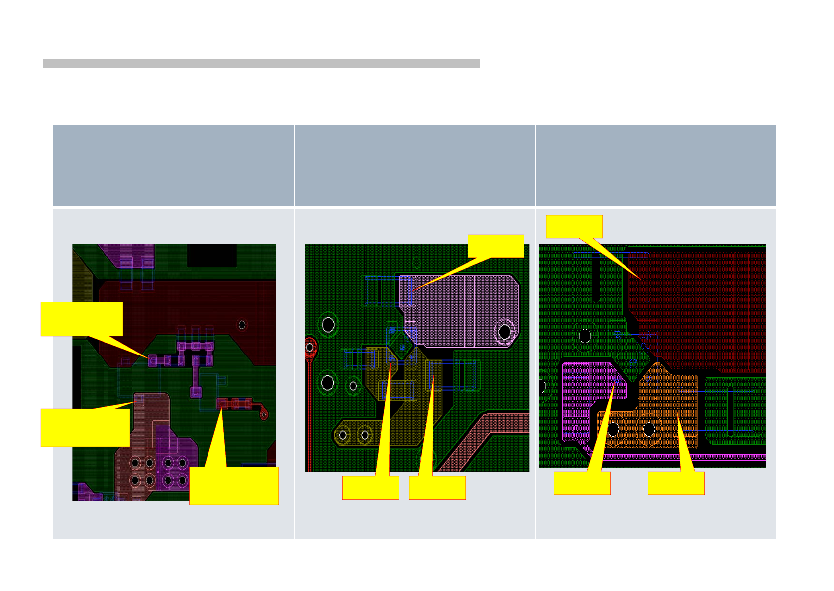
1.3 No Po wer DDC ON/L DO
DDC & LDO Locations
DDC: +3.3V_MAIN DDC:
+1.05V_M2_STBY
#PIN2
IC602
Q407
#PIN1
(VG)
Q406
DDC:
+1.05V_M2_ST_ET
C631
C611
IC605
#PIN1
(VB)
#PIN3
C610
#PIN3 C630
49
Page 50
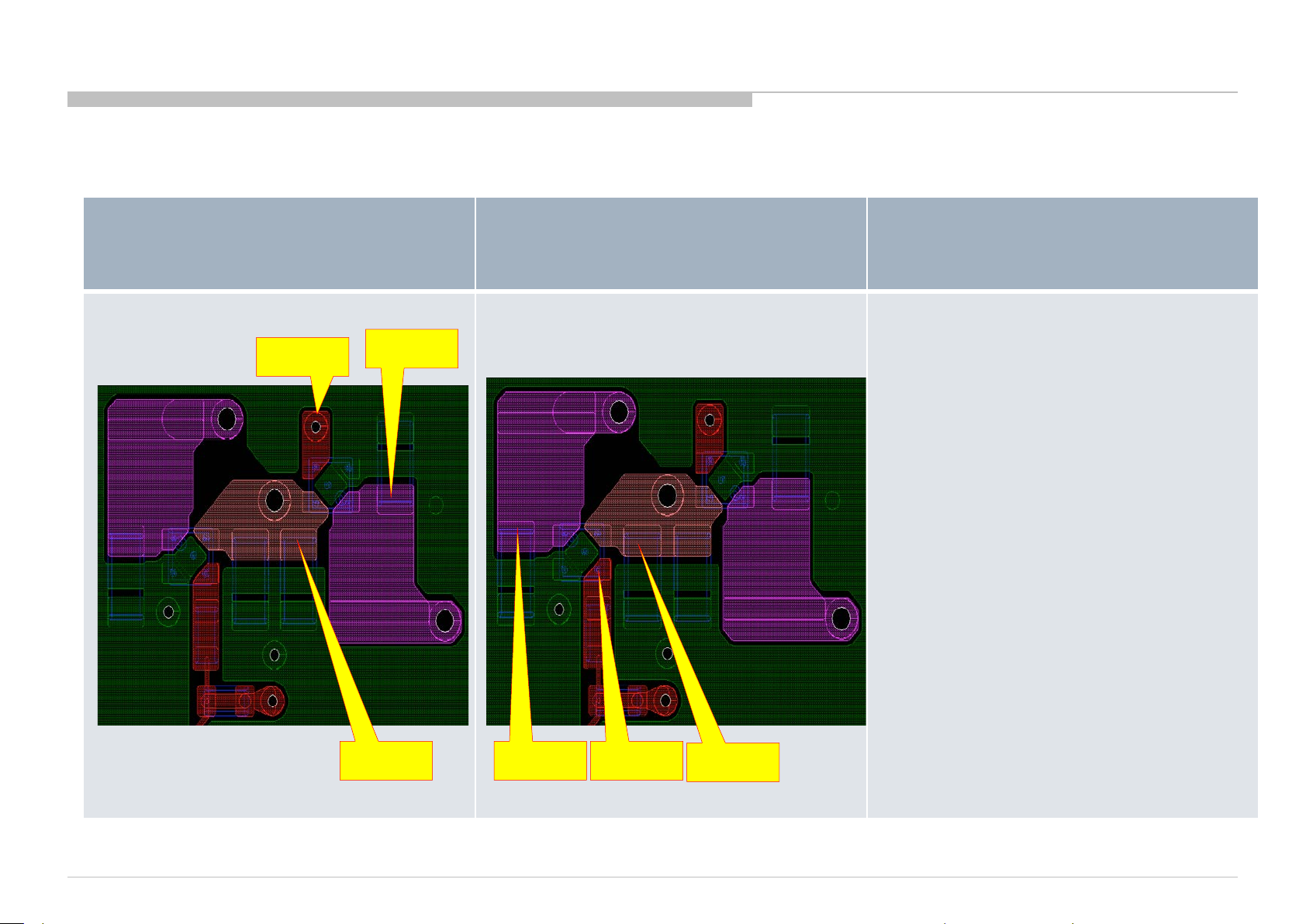
1.3 No Po wer DDC ON/L DO
DDC & LDO Locations
DDC:
+1.05V_M2_A_1
#PIN3
IC606 IC603
C613
+1.05V_M2_A_2
DDC:
C612
C633 #PIN3
C632
50
Page 51
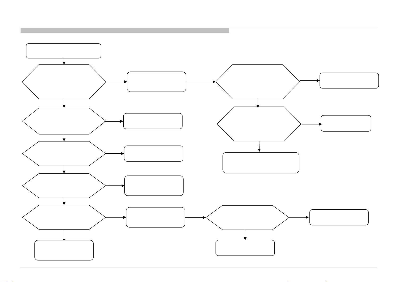
1.4 NO POWER – Muffin2 Failure
Muffin2 Fail S uspec ted
Muffin2 LOG is
displayed
No
Power uCom and
DDCON/LDO OK?
Yes
Crystal X1000
Is there 24MHz?
Yes
Muffin reset released?
ORESETB=High
Yes
eMMC clock present?
Yes
No
No
No
Yes
Write DDR check
bootloader
Follow 1.2&1. 3
Replace cr ystal
Check uCom
Follow 1.2
Write DDR check
bootloader
Is there DD R error?
No
Check M uffin Log
related to eMMC
Is there “CRC error”
No
Store SW log, check SW
behaviors.
Is there DD R error?
Yes
Replace DDR
Yes
Replace eMMC
Yes
Replace DDR
No
Replace M uffin
No
eMMC
data corrupti on
51
51
Page 52
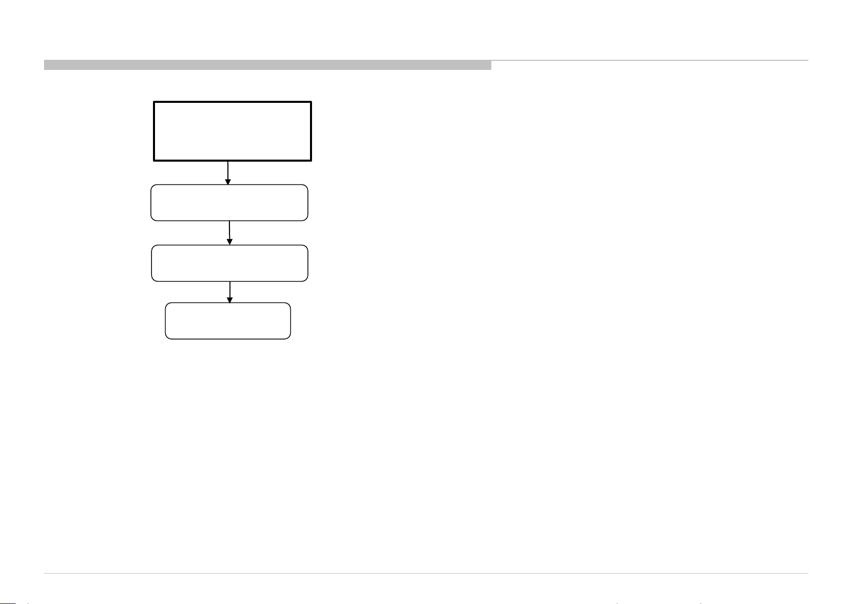
1.4 NO POWER – Muffin2 Replacement
Muffin2
replacement
flow
Data on eMMC need to be
eMMC erase
Muffin2 replacement
SW write
erase first before changing
Muffin
If cannot be erased, erase
after replacing Muffin
52
52
Page 53
2.0 LED Blinking: 2x (Main power Error)
BFX(G* Board model)
2-time blinking
Check “+12V_MAIN”
at pin 11/13 of CN400
on BFX Board,
Voltage > 13.2V ?
No
Yes
G* Board
BFX(AC adapter model)
2-time blinking
Check “+12V_MAIN”
at pin 11/13 of CN400
on BFX Board,
Voltage > 13.2V ?
No
Yes
LD Board
BFX Board
BFX Board
53
53
Page 54
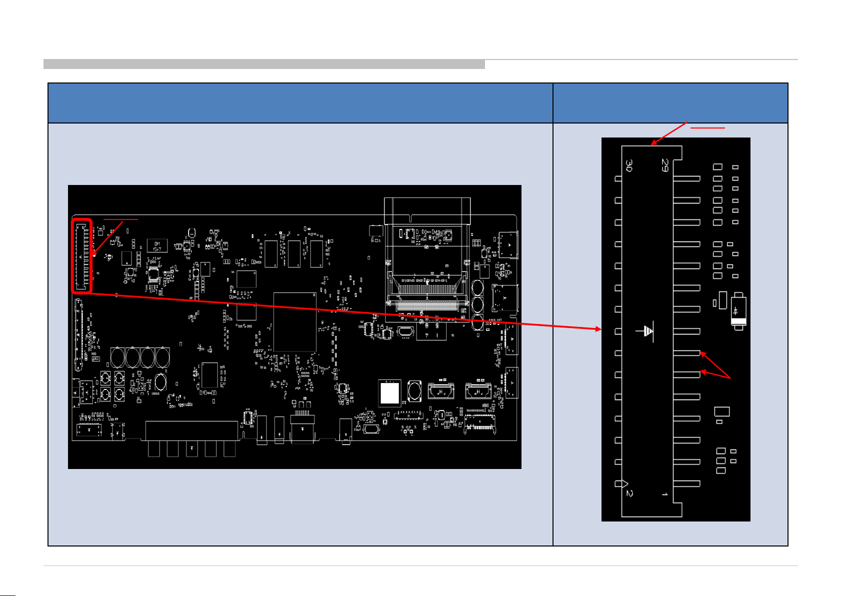
Check point for BFX
BFX (A side) Detail
CN400
CN400
+12V_MAIN
54
54
Page 55
Detail of 3x LED Blinking
Error
Item
Trinity2 DC_ALERT 3
AUD_ERR 3 Audio amp error detection
Trinity2 Board: BFX;
Number of STBY
LED flashing
Description
Main board 5V power rail
monitoring
55
55
Page 56
2.1 LED Blinking: 3x (DC Alert Error)
BFX
3-time b linkin g
Check
+5.0V_VBUS at “C431”
4.959V<Voltage<5.285V?
NG
IC402,etc
(B* Board)
OK
Audio Error
56
56
Page 57
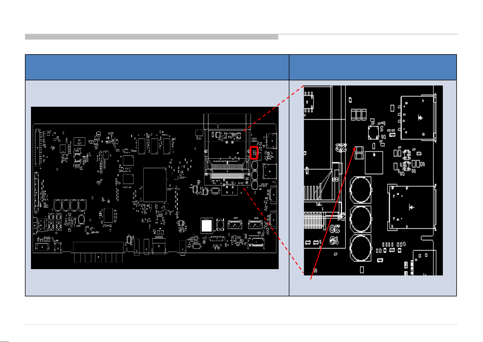
Check point for BFX
Board PWB (A side) Detail
+5.0V_VBUS at “C431”
57
57
Page 58
Detail of 3x LED Blinking
Error
Item
Trinity2 DC_ALERT 3
AUD_ERR 3 Audio amp error detection
Trinity2 Board: BFX;
Number of STBY
LED flashing
Description
Main board 5V power rail
monitoring
58
58
Page 59
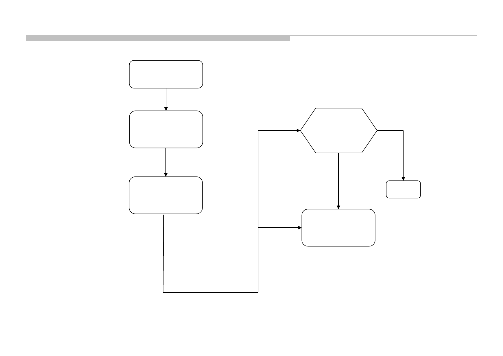
2.2 LED Blinking: 3x (Audio Erro r)
LED 3x blinking
(Audio Error)
Power Off
Check
Power On
Check
Go to
3.3 Power off checking
Go to
3.4 Power on checking
KFW
KF
Replace B-K Harness
OK ?
No
Replace B-Boar d
and
K-Board (KFW only)
For BFX chassis: if with AC adapter,
G-Board refer to LD board
Yes
Finish
59
59
Page 60
Check point for BFX
Name
BFX
B* board (A side)
(1) VCCP-GNDP short check
Measure impedance between
VDD and GND at capacitor
C3267.
If impedance is <100Ω → NG
(3) Fuse open check
Measure impedance of fuse
F3201;
C3239 C3237
If fuse open → NG
F3201
C3267
60
60
Page 61
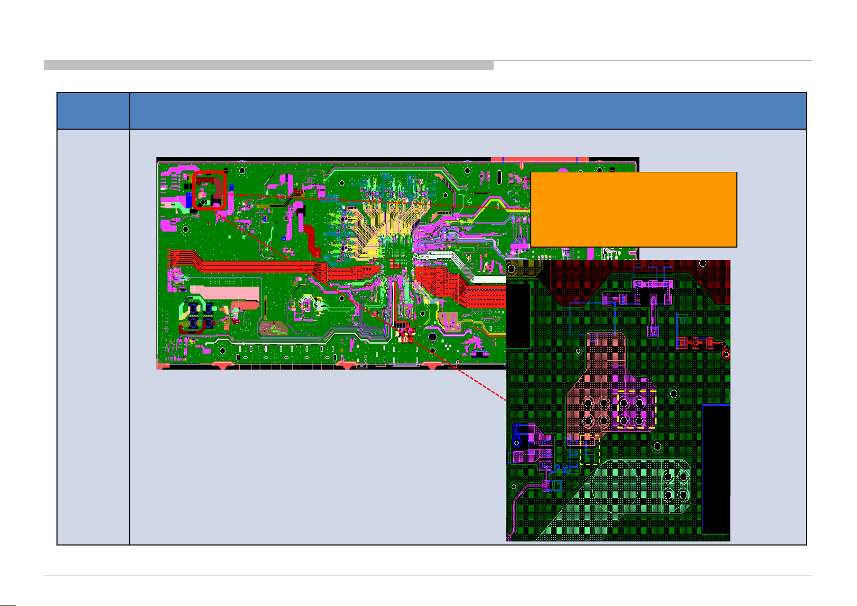
Check point for BFX
Name
BFX
B* board (A side)
(2) +3.3V_Audio out short check
Measure impedance between
C470 and GND.
If impedance is <100Ω → NG
Q407
Q406
+3.3V_Audi
o
IC407
C470
61
61
Page 62
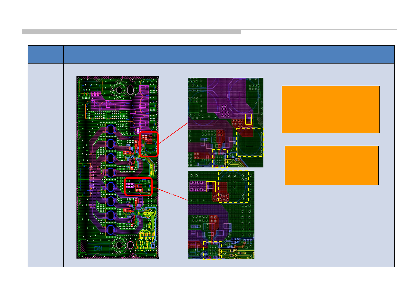
Check point for BFX
Name
KK3
K* board (A side)
IC5501
F5500
F5501
C5524
(1) VCCP-GNDP short check
Measure impedance between
VDD and GND at capacitor
C5581 and C5524.
If impedance is <100Ω → NG
C5581
(3) Fuse open check
Measure impedance of fuse
F5500 and F5501;
If fuse open → NG
IC5500
62
62
62
Page 63
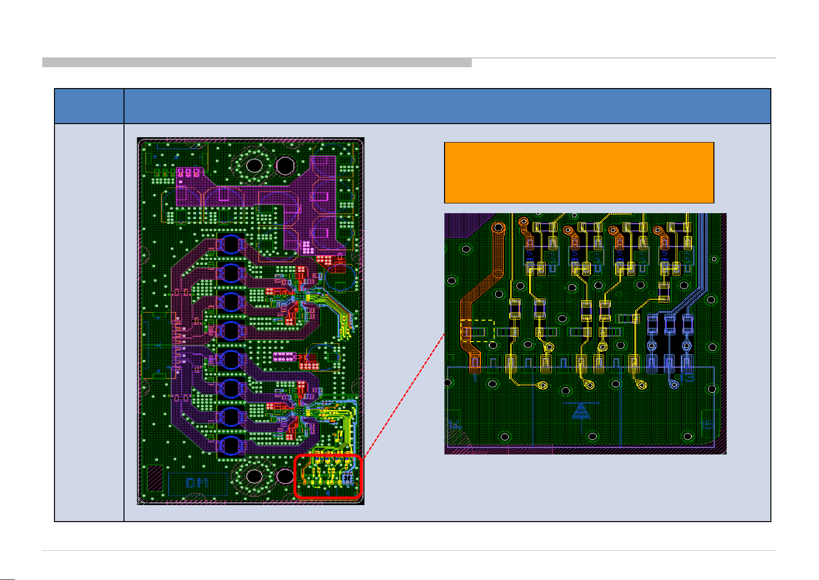
Check point for BFX
Name
KK3
K* board (A side)
(2) +3.3V_Audio out short check
Measure impedance between C5586 and GND.
If impedance is <100Ω → NG
C5586
63
63
63
Page 64
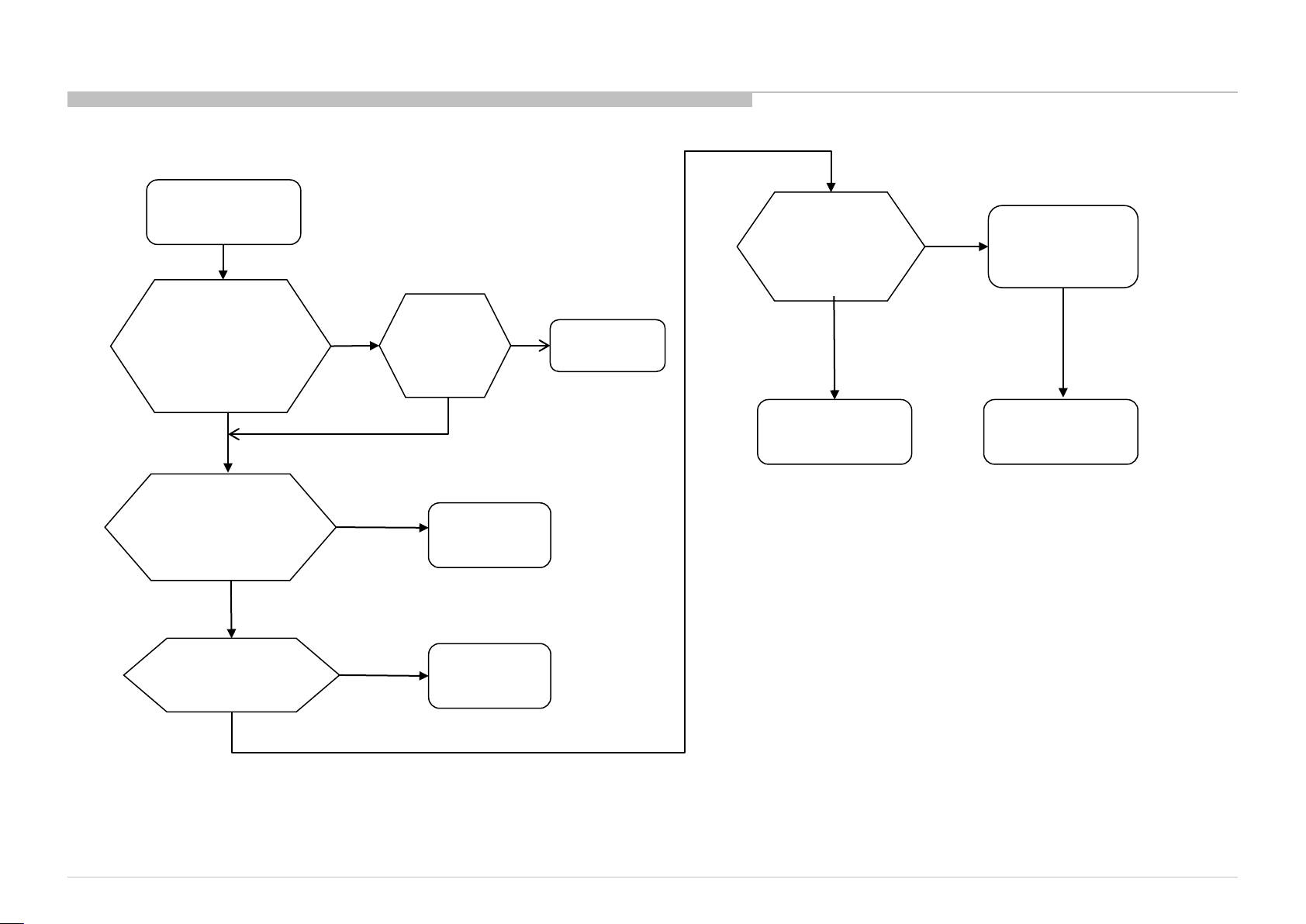
2.4 LED BLINKING: 5x (Panel Communication Error)
BFX
5-times blinking
Check
“+12.5V_TCON”
on BFX
OK
Replace the Harness
Between G/LD* Board
and BFX
NG
Replace
NG
NG
G/LD* Board
OK
OK
Replace
Harness is
broken
V-By-One FFC
OK
G/LD*Board
broken
Change
BFX
BFX is
broken
OK
NG
Change
Panel (T-con)
OK
Panel (T-Con) is
broken
the V-By-One FFC
NG
G/LD* Board: G board or LD board
is broken
64
64
Page 65
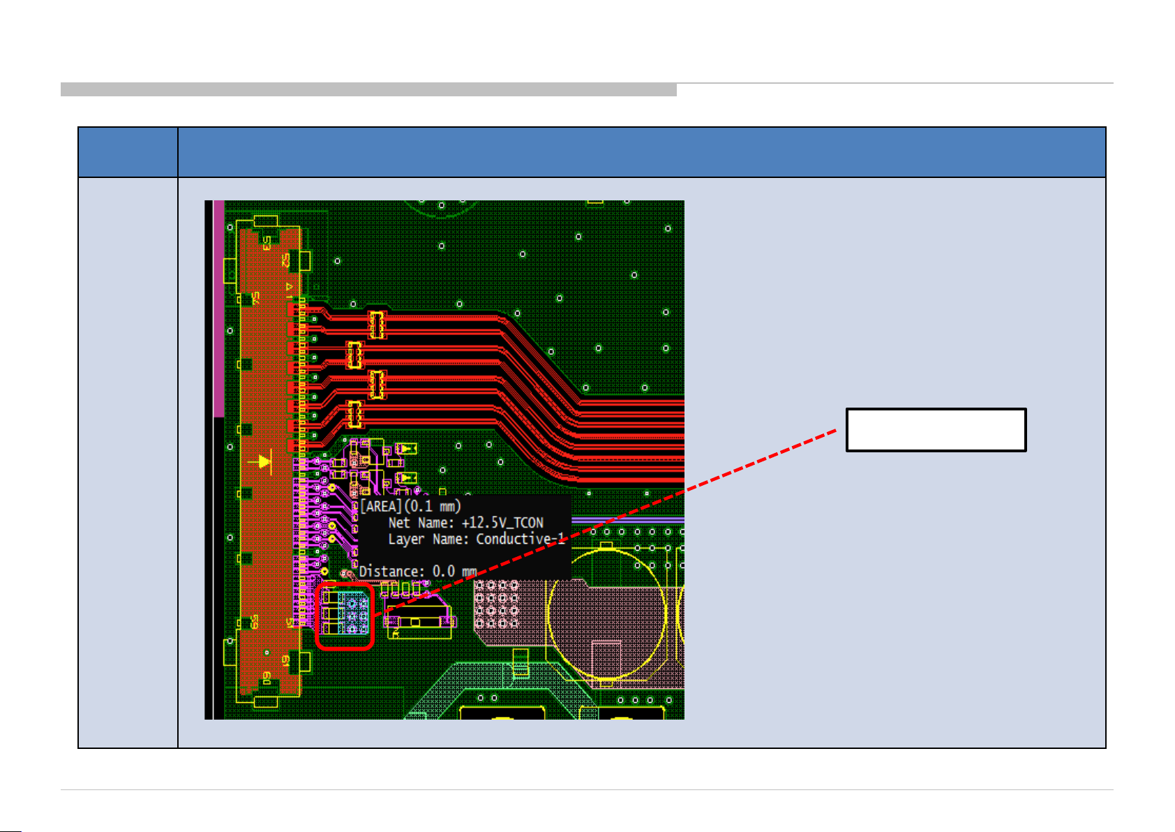
Check point for BFX
Name
BFX
B* board (A side)
+12.5V_TCON
65
65
Page 66
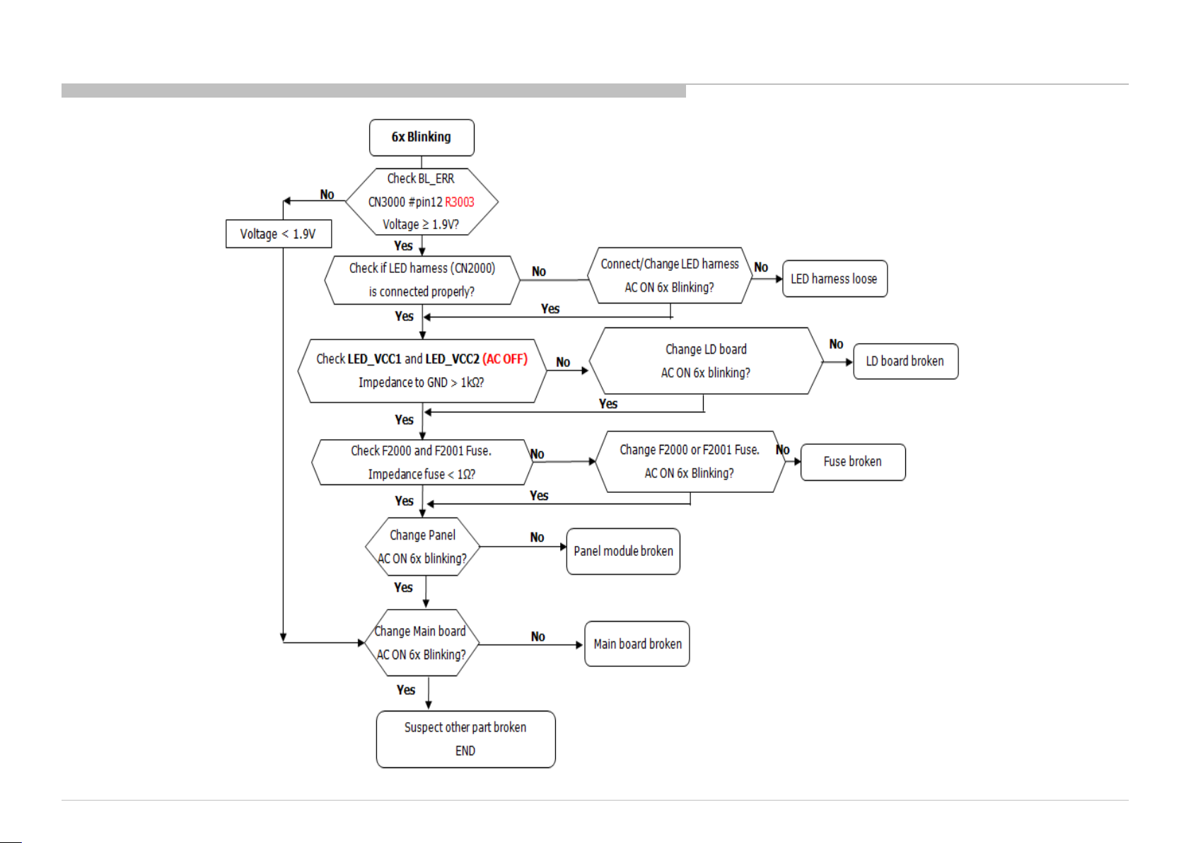
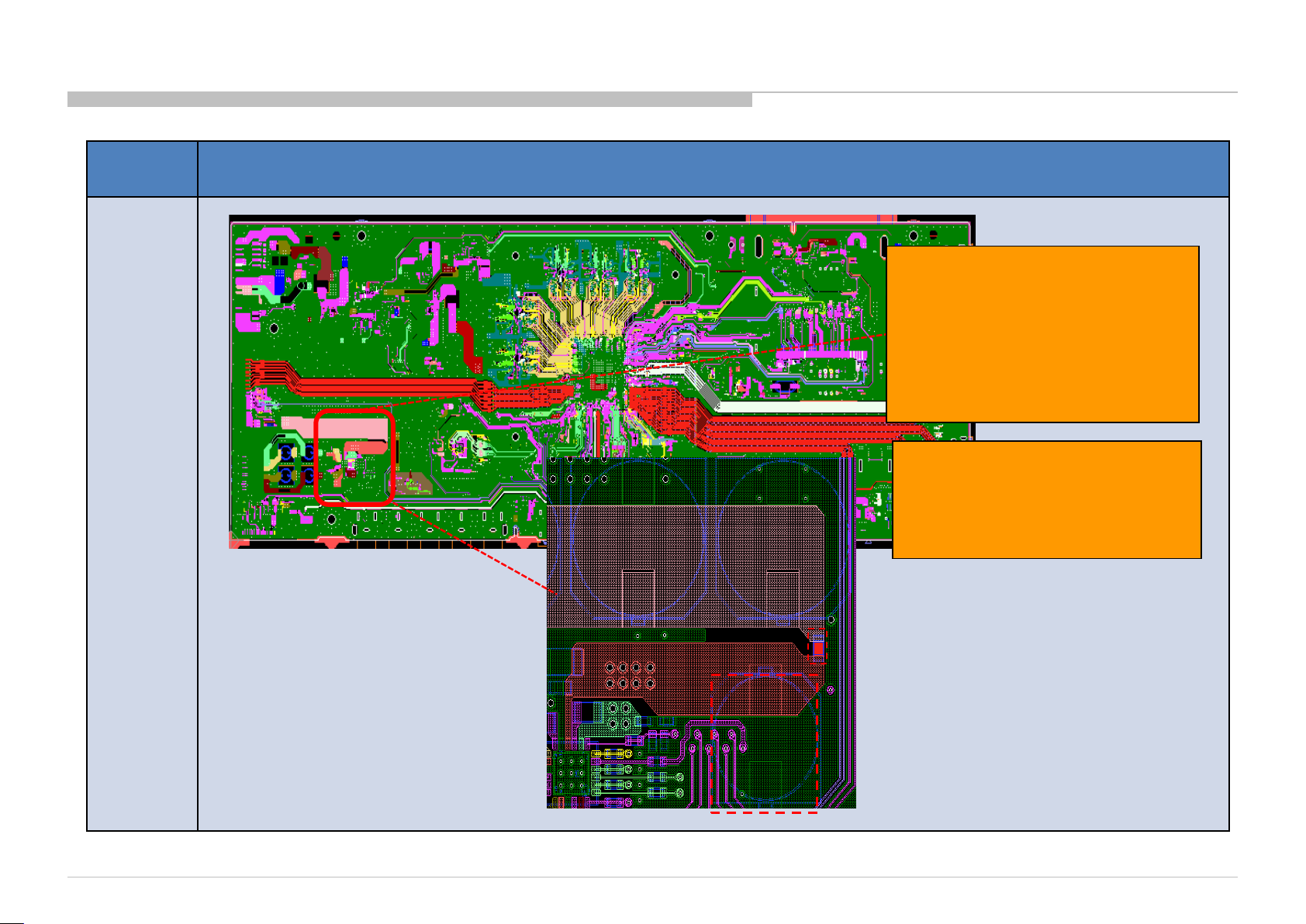
2.5 6x Blinking backlight error
TV Business Division
Check point on PWB refer next slide
66
66
Page 67
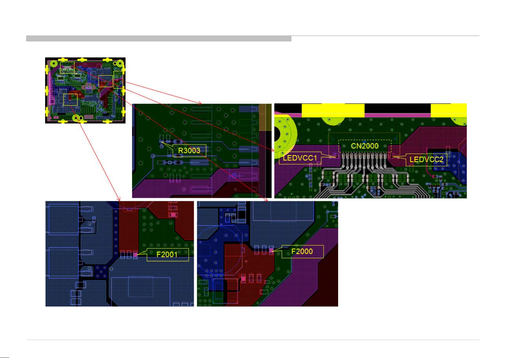
2.5 6x Blinking backlight error
TV Business Division
67
67
Page 68
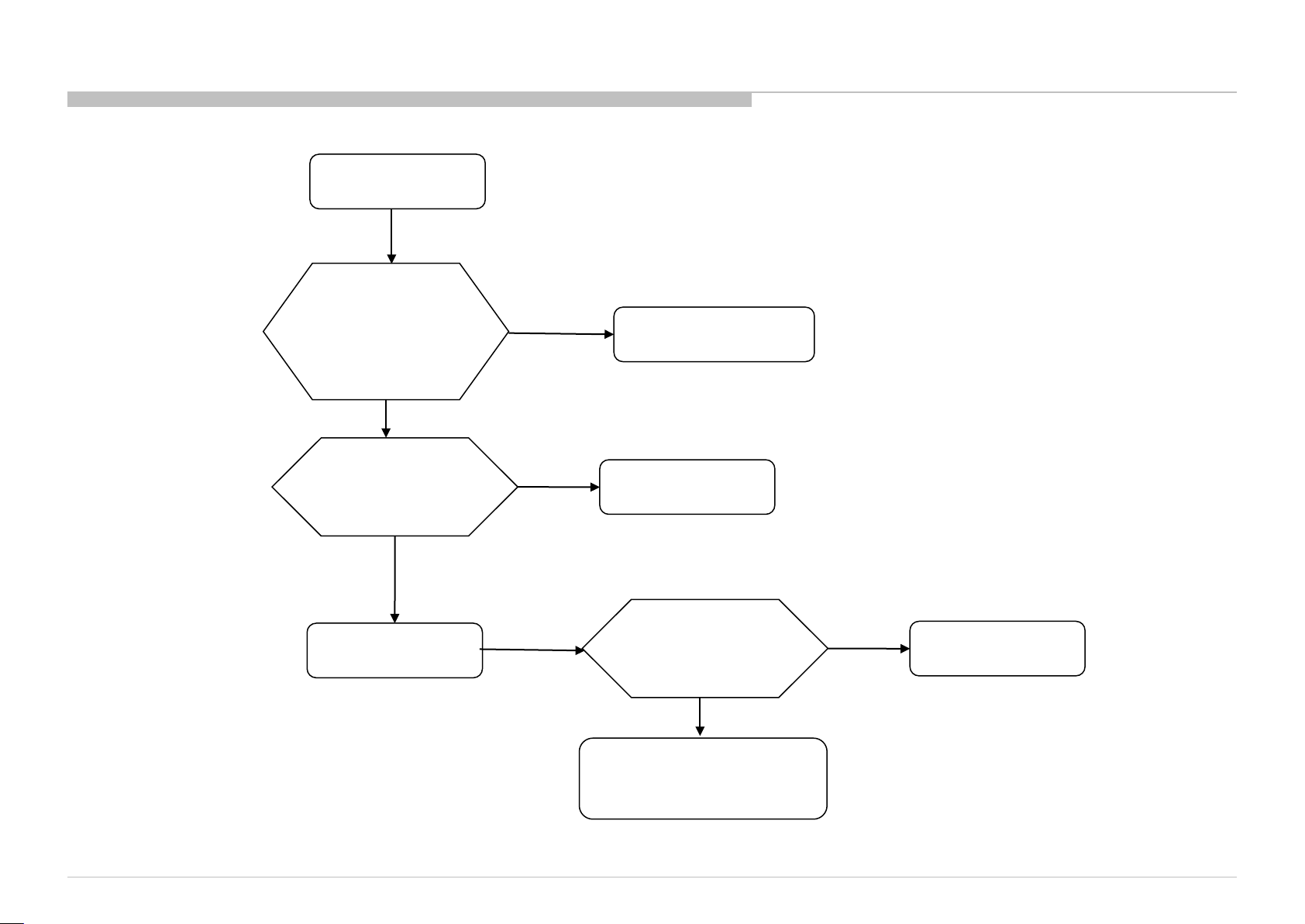
2.6 LED BLINKING: 7x (Temperature Error)
7-time blinking
Setting
circumstance is OK?
Temperature,
Ventilation, et c.
Yes
Change B* Board,
and A ging a few
hours
Symptom
improvement
B* Board NG
No
NG
Set to another
location, etc.
Panel
Check I2C _C bus
communic ation OK?
(check the nex t page)
No
Yes
Temp sensor
I2C_C bus dumpi ng or
Muffin check
68
68
Page 69
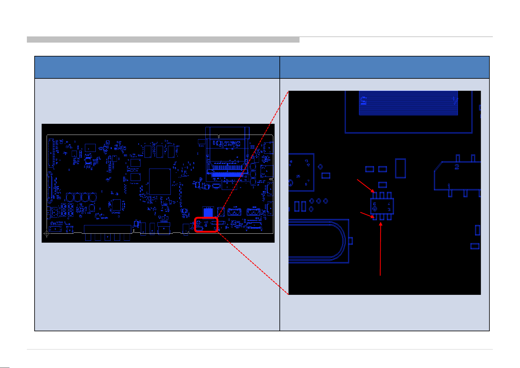
Check point for BFX
BFX board (A side)
KK3
Detail
I2C0_SDA
IC1200
I2C0_SCL
Temperature Sensor
69
69
Page 70
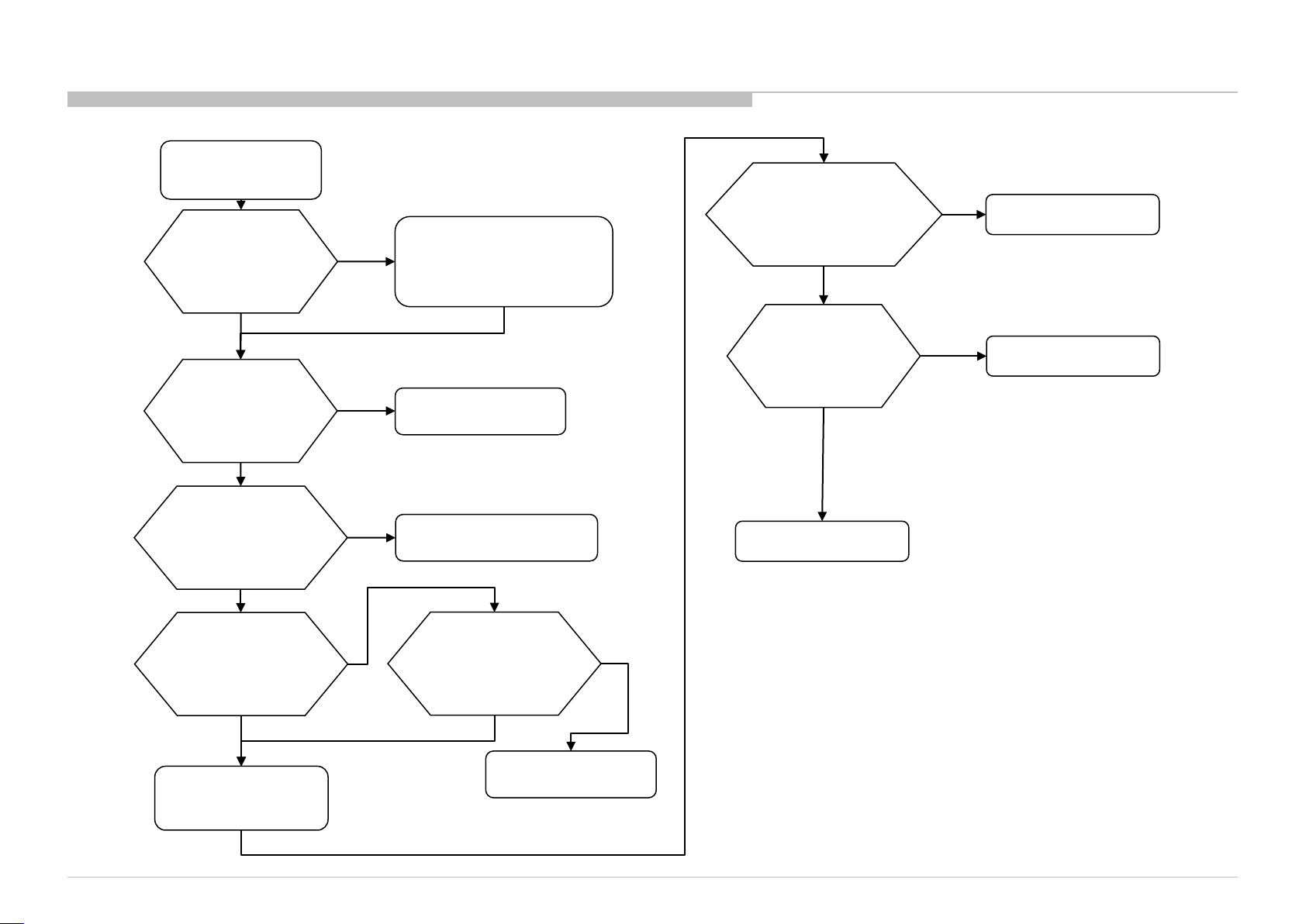
3.0 No Sound
No Sound
Without LED 3x
AV receiver is connected
to HDMI in ?
No
Yes
Select [External Inputs]→
[BRAVIA Sync Settings]→
[BRAVIA Sync Control]→[off]
No sound only
Analog R F and Digital R F ?
No
No sound only HDMI ?
Yes
Yes
Go to
3.7 No Sound Tuner
Go to
3.8 No Sound HDMI
[Speakers] setting is
[Audio System] ?
No
Headphone is connected to
HP/Audio Out terminal ?
No
[Sound]→
[Headphone Speaker Link]
setting is [On] ?
No
Go to
3.3 Power Off Checking
Yes
Yes
Yes
Change the setting to
[TV Speakers]
Disconnect the Headphone
Change [Sound]→
Yes
[Headphone Speaker Link]
to [Off], OK ?
No
Replace B-Board
HP/Audio out terminal or Headphone detect
GPIO may be broken
No
Go to
3.1 No Sound Audio
70
70
Page 71
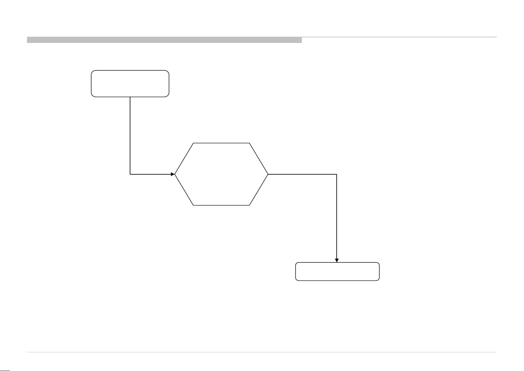
3.1 No Sound Audio
No Sound
Audio
Replace B-Board
And
K-Board*
Finish
*For KF segment: Only replace BFX board
*For KFW s egment: Replace KK3 Board and BFX board
71
71
Page 72
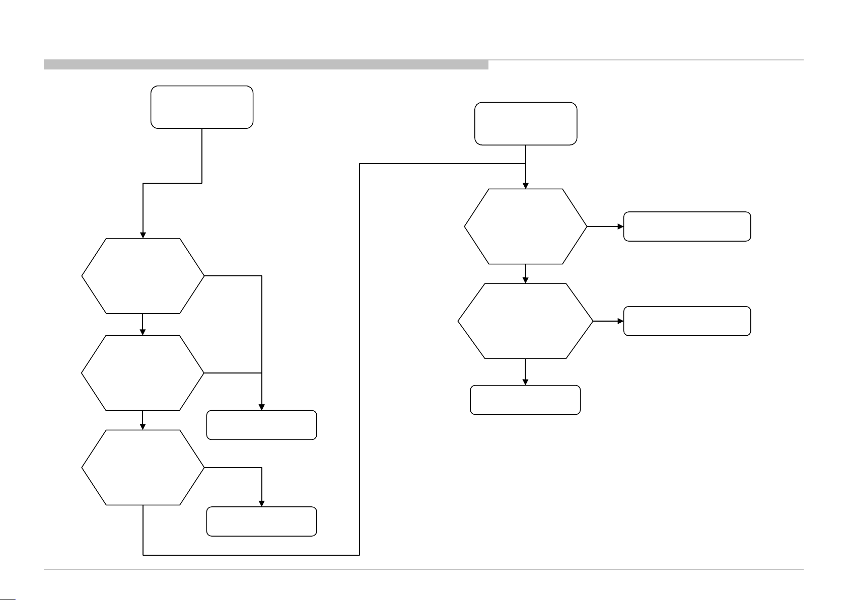
3.3 No Sound Power Off Check [KF/KFW]
Power Off Check
(1) B-Board*
PVDD-GND short ?
(See next p age)
No
(2) B-Board*
LDO out short ?
(See next p age)
No
From 2.2
Yes
Yes
Replace B-Board*
Power Off Check
Measure the Speaker
impedance by multi-meter
Less than 3Ω or
open (broken) ?
Confirm the speaker
to the chassis ?
Return to 2.1 or 3.0
From 3.0
No
harness
Cut or shorted
No
Yes
Yes
Replace Speaker
Replace Speaker Harness
(3) B-Board*
Fuse broken ?
(See next p age)
No
Yes
Change Fuse
*For KFW: B-Board refer to K-Board
72
72
Page 73
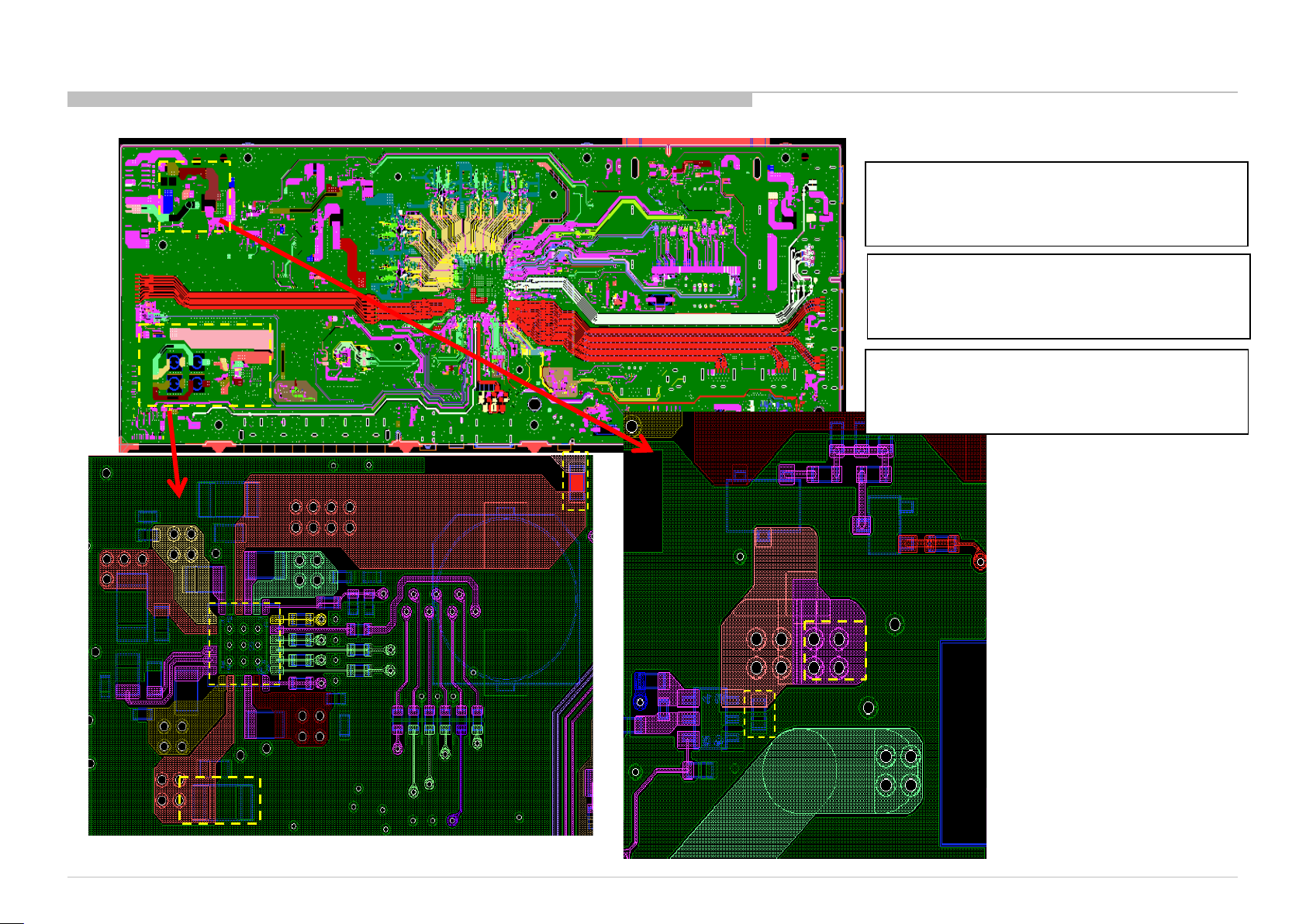
BFX-Board [ KF only]
(1) PVDD-GND short check
Measure impedance between PVDD and GND at
capacitor C3262.
If impedance is <100Ω → NG
(2) LDO out short check
Measure impedance between +3.3V_Audio and GND
at C470.
If impedance is <100Ω → NG
(3) Fuse open check
Measure impedance of fuse
F3201 5A (12.5V or 19.5V)
If fuse open → NG (Change Fuse)
F3201
Q407
IC3202
C3262
C3267
+3.3V_Audio
IC407
C470
73
73
Page 74
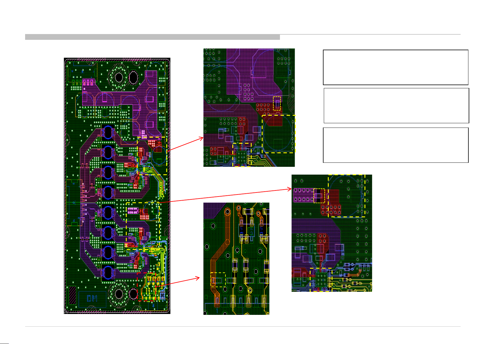
KK3-Board [ KFW only]
F5501
(1) PVDD-GND short check
Measure impedance between PVDD and GND at
capacitor C5581 and C5524.
If impedance is <100Ω → NG
(2) LDO out short check
Measure impedance between +3.3V_Audio and GND
at C5586.
If impedance is <100Ω → NG
IC5501
C5586
C5581
(3) Fuse open check
Measure impedance of fuse
F5500 and F5501 [5A] (12.5V or 19.5V)
If fuse open → NG (Change Fuse)
F5500
C5524
IC5500
74
74
Page 75
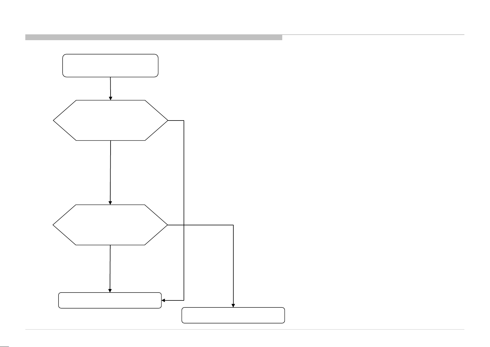
3.4 No Sound Power On Check [KF/KFW]
Power On Check
From 2.2
*POWER_AU is same as PVDD
(4) POWER _A U * check
POWER_AU is supplied to
B-Board* for a moment
before LED 3x blink i ng ?
Replace LD-Board**
No
No
OK ?
No
Yes
Yes
Return to 2.1
Finish
* For KFW, B-Board refer to KK3-Board
**For BFX chassis: If non AC adapter model, LD-Board
refer to G board;
75
75
Page 76
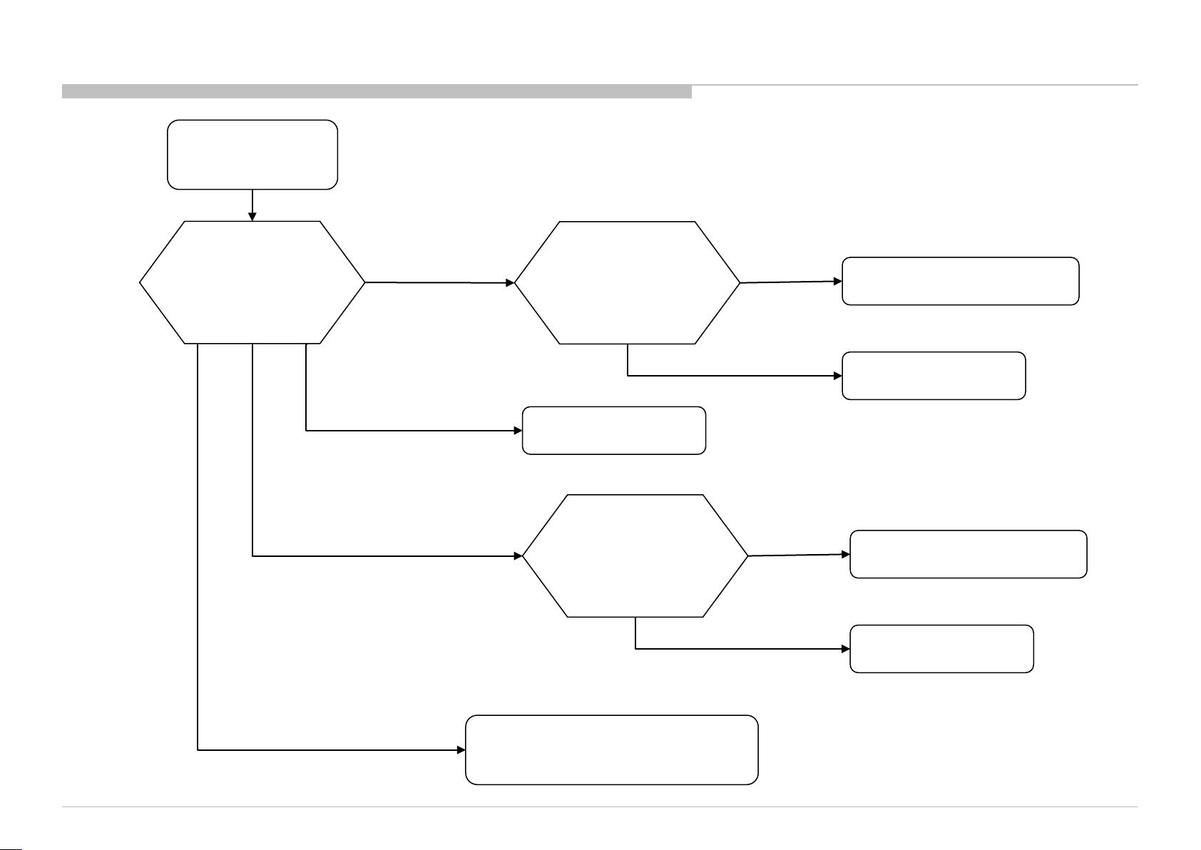
3.5 No Sound Audio HP/ Audio out
No Sound Audio
HP/Audio out
[Sound]→
[Headphone/Audio out]
is set to ?
[Audi o Out (Variable)]
[Headphone]
[Audi o Out (Fixed)]
Headphone Volume
is set to MIN?
Replace B-Board
Volume
is set to MIN?
Yes
No
Yes
No
Increase Headphone Volume
Replace B-Board
Increase Volume
Replace B-Board
[Subwoofer]
Set [Headphone/Audio Out]
to [Headphone] or [Audio Out]
76
76
Page 77

3.6 [ Not Applicable ]
77
77
Page 78
3.7 NO SOUND: @ TUNER
No Sound with normal picture
Only RF tuner input?
YES
NO
Check IC1000 (SOC)
Please refer Audio
troubleshooting
78
78
Page 79
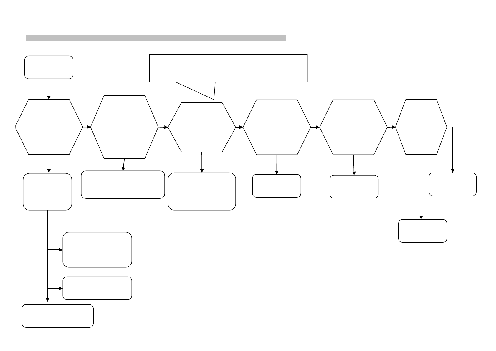
4.0 No Picture
No Picture
Got Any Normal
Display?
Yes
Check Other
Portion:
BL_ON (L or H): IC401 Pin #18 (BFX
board)
Check Smart Core
LED Indication
No
Troubleshooting manual
(5x Blinking)
Yes
Refer 5x Blinking
No
BL_ON:H
Check
BL_ON
on the main board
BL_ON:L
Refer to Backlight
Troubleshooting
Manual
Replace
the V by One FFC
Harness
OK
V by One FFC
Harness NG
NG
Replace
the main Board
Main board NG
OK
NG
Replace
LD/G Board
NG
LCD Panel
OK
LD/G Board NG
Ext. Video Input -
No Picture
HDMI - No Picture
Tuner - No Picture
(T-CON) NG
79
79
Page 80
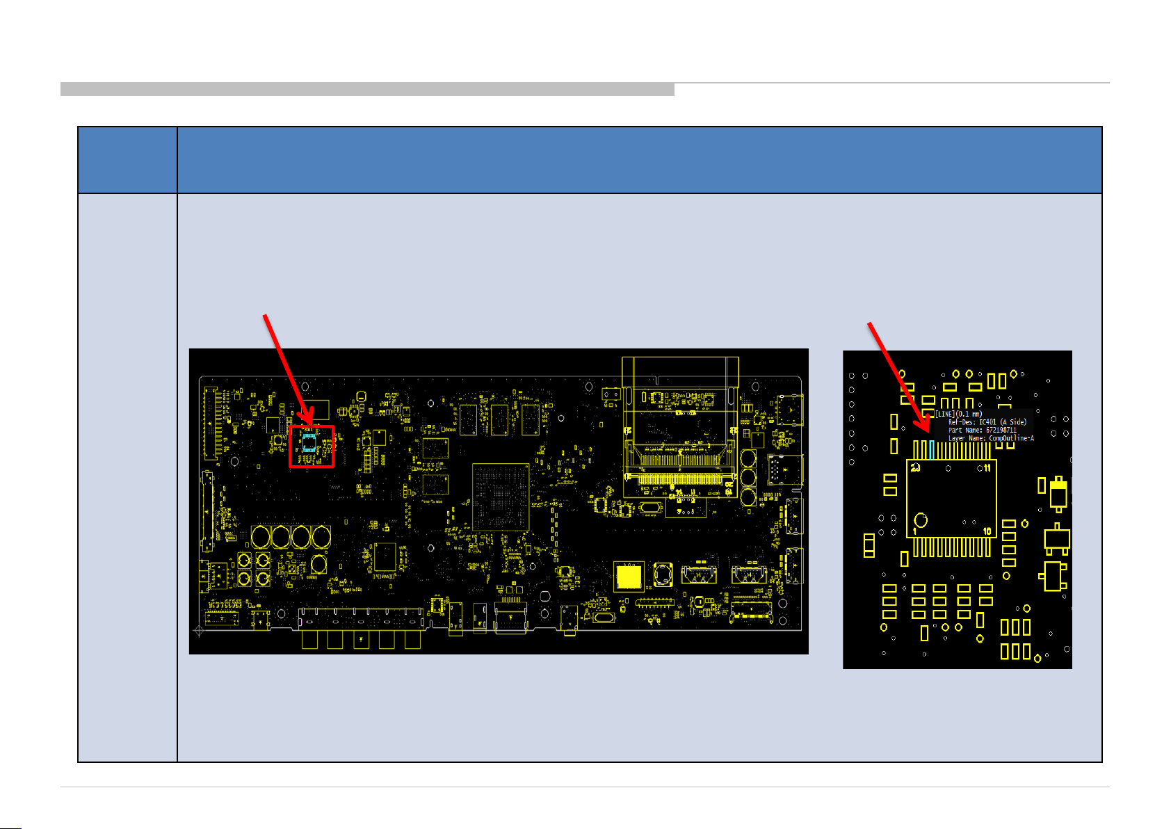
BL_ON (IC401: Pin #18)
Board
Name
BFX
Board PWB A-side
IC401
Pin #18
80
80
Page 81
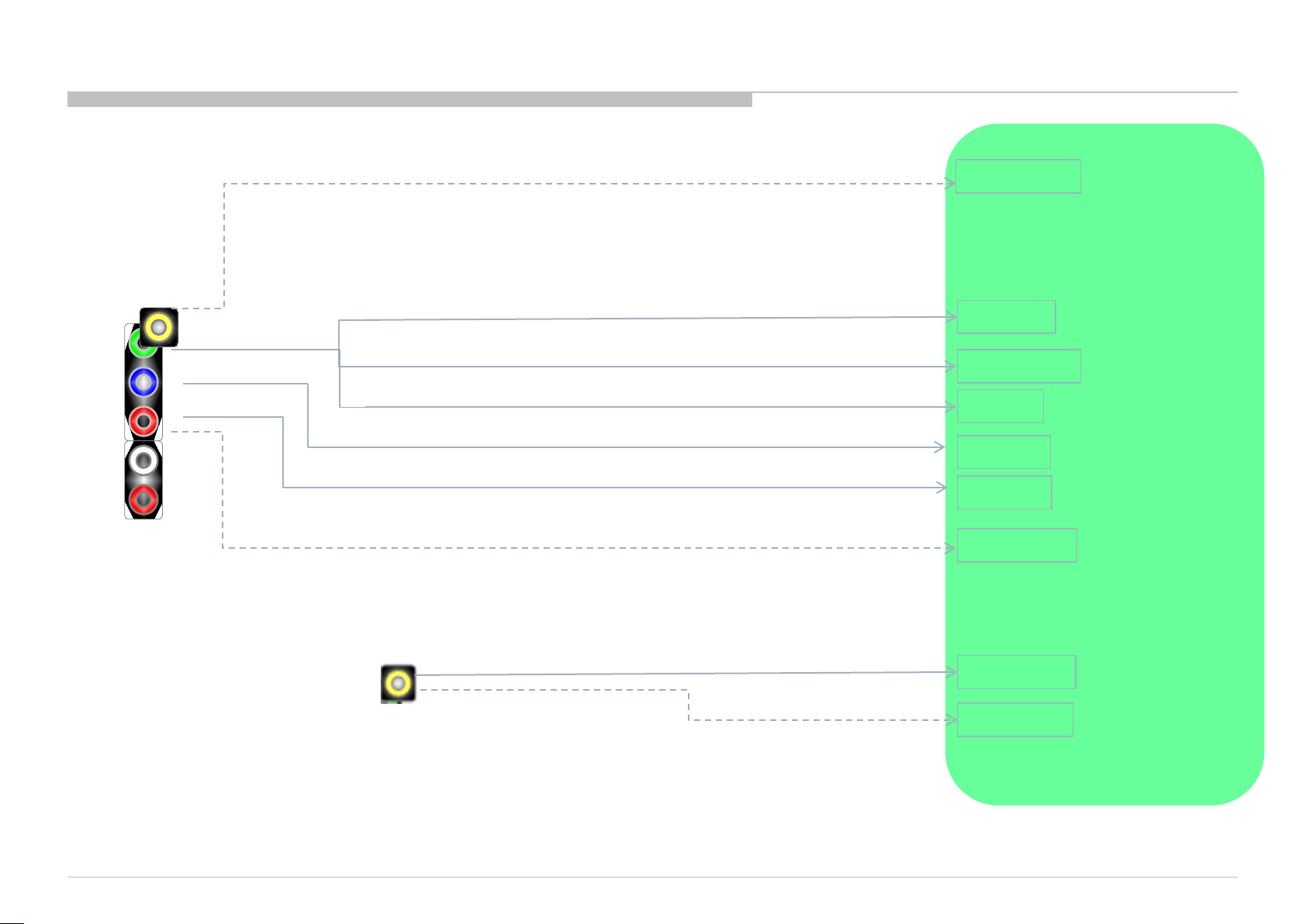
4.1 : Video Analog Signal Path
VIDEO_DET
Video2/Component
(Rear)
SCART_FB/COMP_Y
CVBS2P
SCART_SB/COMP_Y
SCART_SG/COMP_PB
AT35:GPIO56
N35:SOY0
M35:CVBS2P
M38:Y0P
L38:PB0P
M2
CR_DET
Video 1
(Rear Conversion
Jack)
SCART_SR/COMP_PR
CVBS3P
VIDEO2_DET
L37:PR0P
A16:SD_CLK
L36:CVBS3P
G16:GPIO66
IC1000
81
81
Page 82
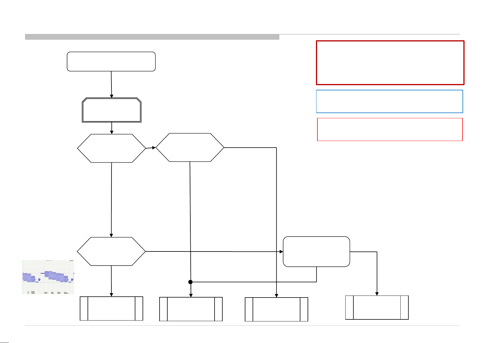
4.2 : No Picture ALL Des tination (BFX)(Conversion Jack)
Checking co ndition:
- TV ON & Video/CVB S/Compo site inp ut cab le is
No Picture
Video 1
No Picture
Check if input OSD
is GREY OUT
OK if it is highlighted
OK
NG
* Chec k J2601
Connection,
VIDEO2_DET
At R2631
NG (V: 0V)
OK (V: 3.3 V)
[All voltage measurement using Oscilloscope]
connected to Video/CVBS/Compo site source
output.
- TV UI Display : Video 1
* OK Condition : No solder splash can be seen
NG Condition : Solder splash can be seen
** OK Condition : No part short-circuited
NG Condition : Part short-circuited
Check wave between
after C2628 and I C 1000
OK (Vpp: 1 V)
Muffin [IC 1000]
Problem
NG (Vpp: 0 V)
J2601 Connector
Problem
** Chec k condition of parts
[D2609/R2629/R2621/C2612
J2601 Connectivi ty
Problem
/R2643]
OK
NG
Parts Broken
82
82
Page 83
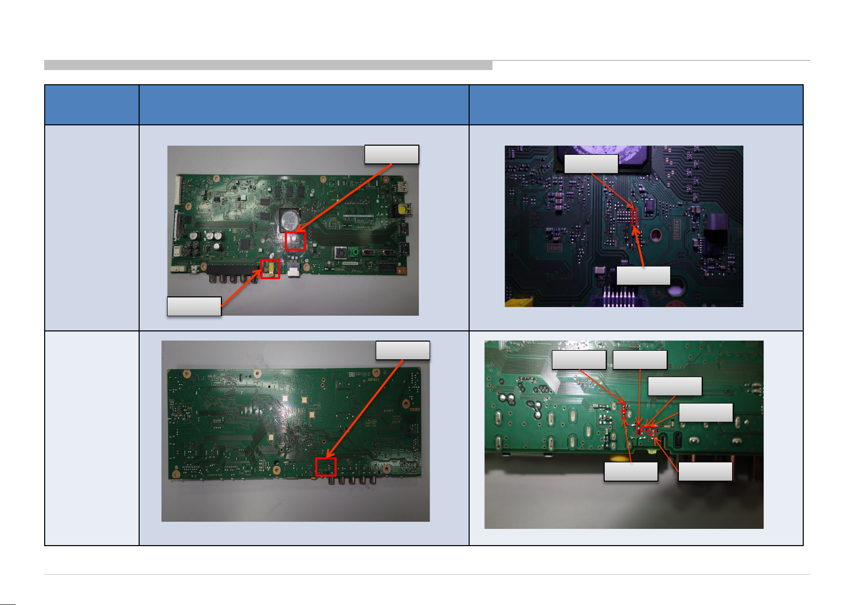
4.21- Video Analog Signal Path - Checking Point
Board
Name
BFX(A-Side)
J2601
C2628
R2643
BFX(B-side)
R2630
R2631
D2609
R2629
R2621
C2612
Board PWB (A side) Detail
Details
J2601
Details
C2628
R2631
R2643
D2609
R2630
R2629
C2612
R2621
83
83
Page 84
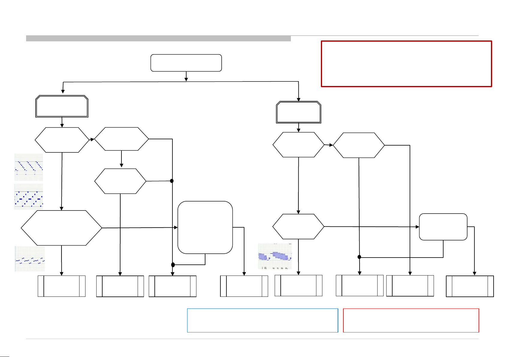
4.3 : No Picture ALL Destination (BFX)(Component)
Checking co ndition:
- TV ON & Video/CVBS/Composit e/Component input
No Picture
Component
Video 2
No Picture
No Picture
cable is connected to
Video/CV BS/Composite/Comp onent source output.
- TV UI Display : Video 2/Component
Check if input OSD
is GREY OUT
OK if it is highlighted
Y : 1V
Pb : 0.7V
Chec k wa ve b etw e e n af t er
(Y:C2602/C2 627), (Pb:C2605),
(Pr:C2607)an d IC1000
Pr : 0.7V
Muffin [IC 1000]
OK
OK
Problem
NG
* Check J2600 Connector,
CR_DET at R2650
OK (Vpp: 3.3 V)
Check VIDEO_DET signal
Path at R2627
NG
J2600 Connectivi ty
Problem
NG (Vpp: 0 V)
NG (Vpp: 0 V)
OK (Vpp: 3.3 V)
J2600 Connector
** Check condition of parts:
Y0P : [VD2602/D2601/R2606/
C2603/R2604]
PB0P : [VD2603/R2603/C2601/
PR0P : [VD2601/R2610/C2606/
S0Y : [R2642]
Problem
R2607]
R2611]
OK
NG
Parts Broken
Check if input OSD
is GREY OUT
OK if it is highlighted
OK
Check wave between
after C2611 and
IC1000
OK (Vpp: 1 V)
Muffin [IC 1000]
Problem
NG
NG (Vpp: 0 V)
* Check J2600
Connection,
VIDEO_DET
J2600 Connector
At R2626
NG (Vpp: 0 V)
Problem
OK (Vpp: 3.3 V)
J2600 Connectivi ty
Problem
** Check condition of parts
[D2601/VD2602/R2606/
C2603/R2619]
OK
Parts Broken
NG
[All voltage measurement using Oscilloscope]
* OK Condition : No solder splash can be seen
NG Condition : Solder splash can be seen
** OK Condition : No part short-circuited
NG Condition : Part short-circuited
84
84
Page 85
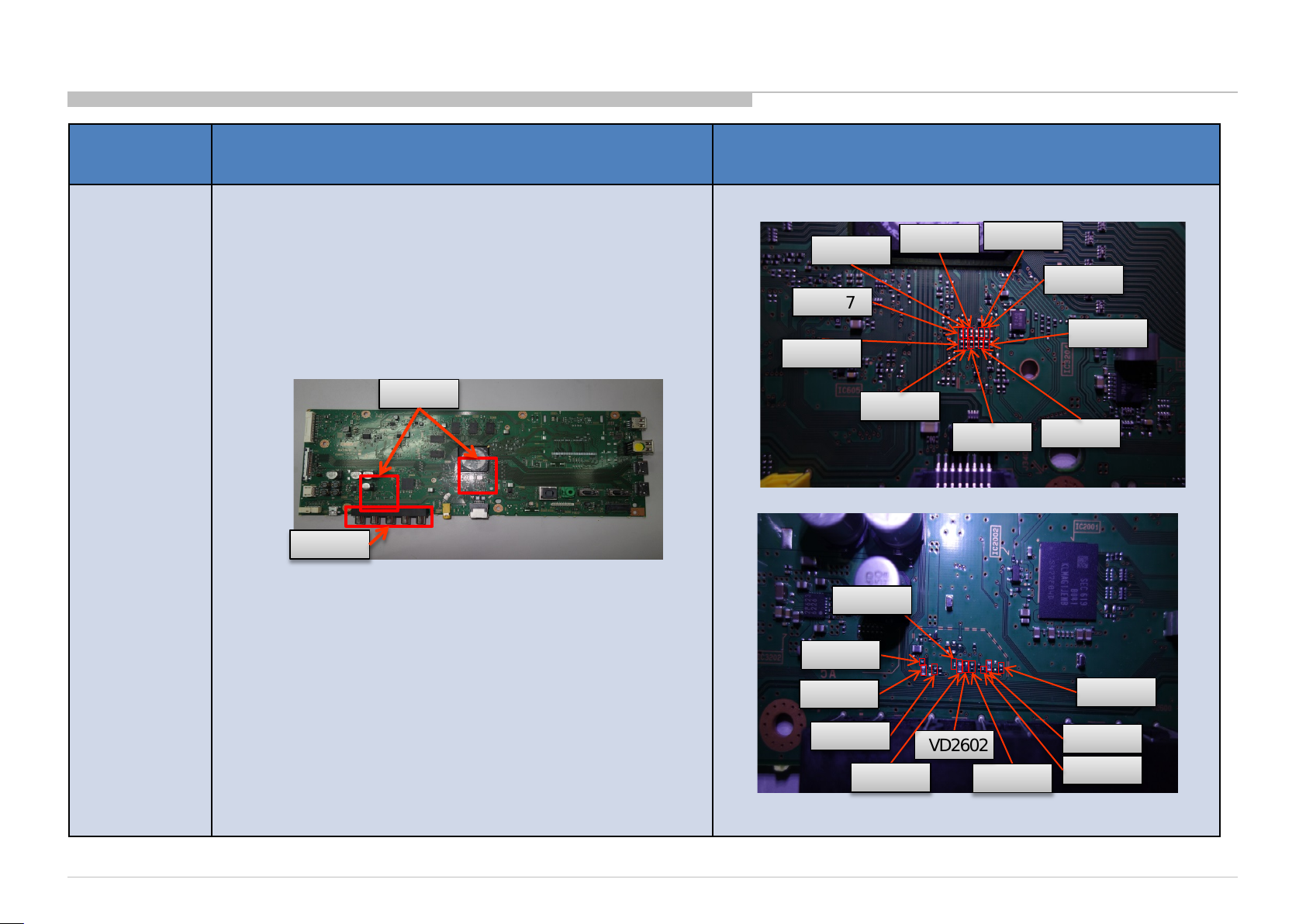
4.31- Video Analog Signal Path - Checking Point
Board
Name
BFX(A-Side)
J2600
C2602
C2605
C2607
C2627
VD2602
D2601
R2606
C2603
R2604
VD2603
R2603
C2601
R2607
VD2601
R2610
C2606
R2611
R2642
R2619
C2611
Board PWB (A side) Detail
Details
J2600
C2611
C2627
R2642
C2606
R2610
VD2601
R2619
R2631
C2603
R2606
C2602
R2630
VD2602
C2605
R2604
D2609
VD2602
C2607
R2611
R2607
R2629
C2612
VD2603
R2621
R2603
C2601
85
85
Page 86
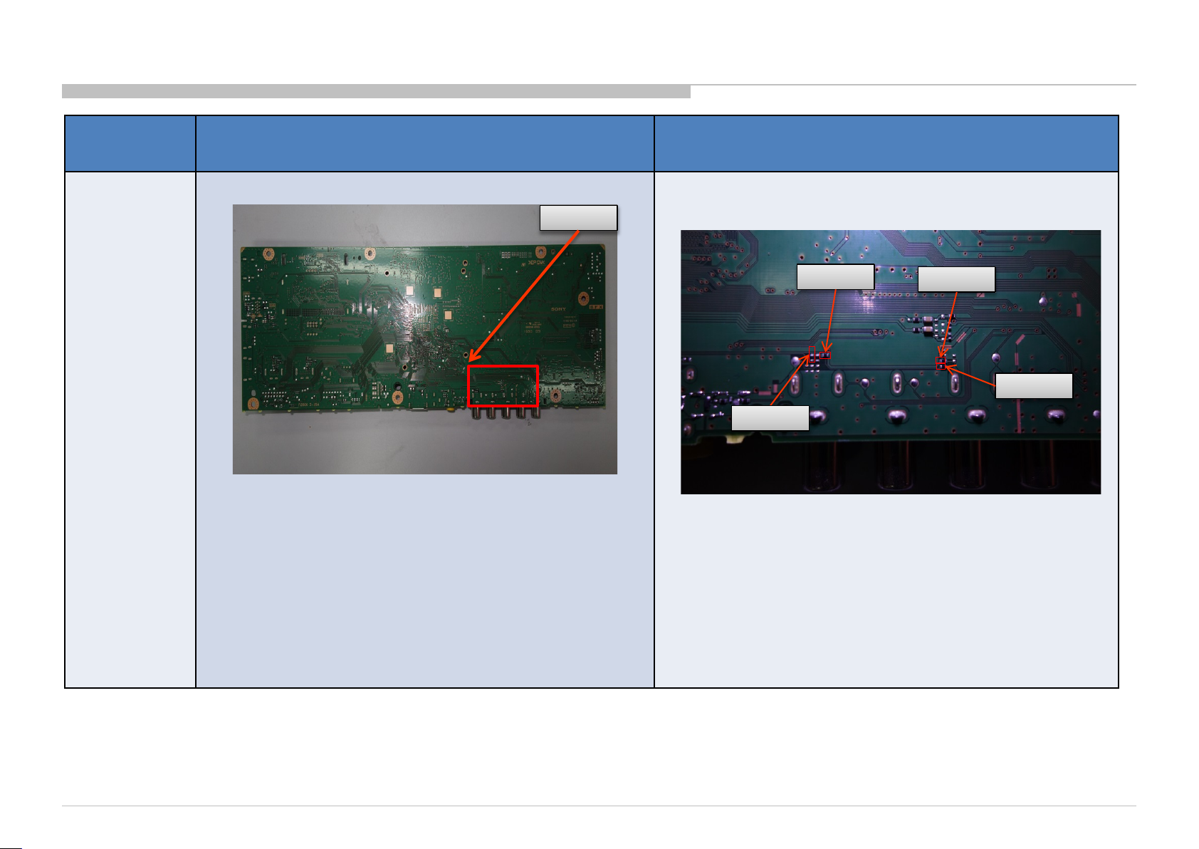
4.31- Video Analog Signal Path - Checking Point
Board
Name
BFX(B-side)
R2626
R2650
R2627
R2637
Board PWB (A side) Detail
Details
R2626
R2627
R2637
R2650
86
86
Page 87
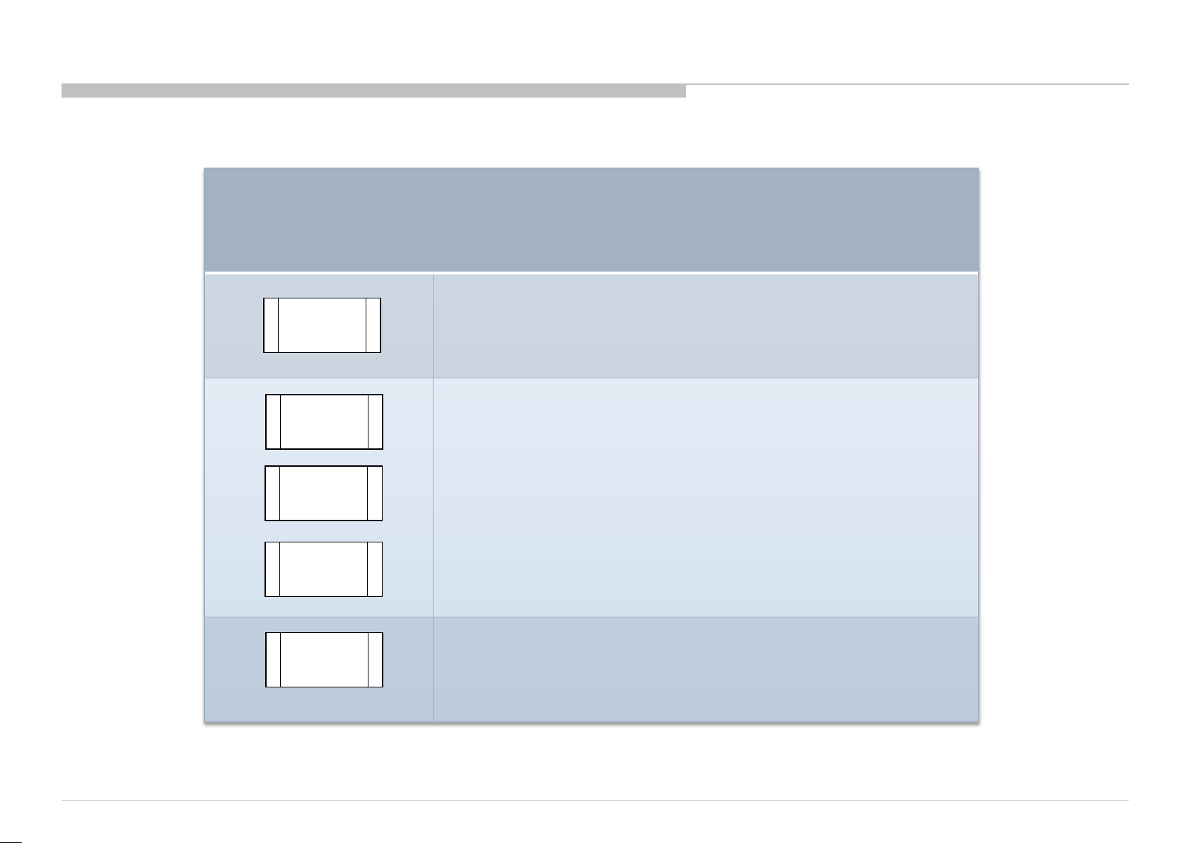
Condition Actions to b e taken
Muffin [IC 1000]
Problem
CN2600 Connecti vit y
Problem
J2601 Connector
Problem
J2600 Connectivi ty
Problem
Parts Broken
Refer to IC troubleshooting
for further investigation
Change Connector
Change Part according to **
remarks
87
87
Page 88
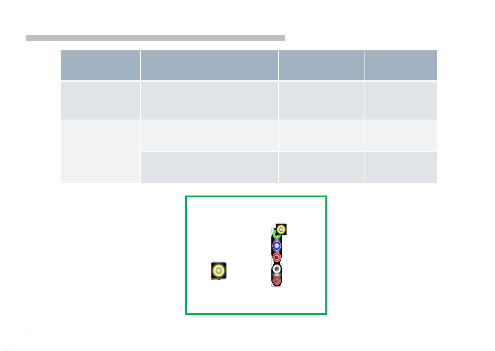
4.2/4.3 : Input Ski p function (BFX)
Input
Signal
Video 1 VIDEO2_DET
IC1000 G16-GPIO66
Video 2 /
Component
VIDEO_DET
IC1000 AT35-GPIO56
CR_DET
IC1000 A16-SD_CLK
Non-Detect
(Typical)
Video 2 / Component
0V
0V
0V
Detect
(Typical)
3.3V
3.3V
3.3V
Video 1
(Rear Mini Jack)
Rear
88
88
Page 89
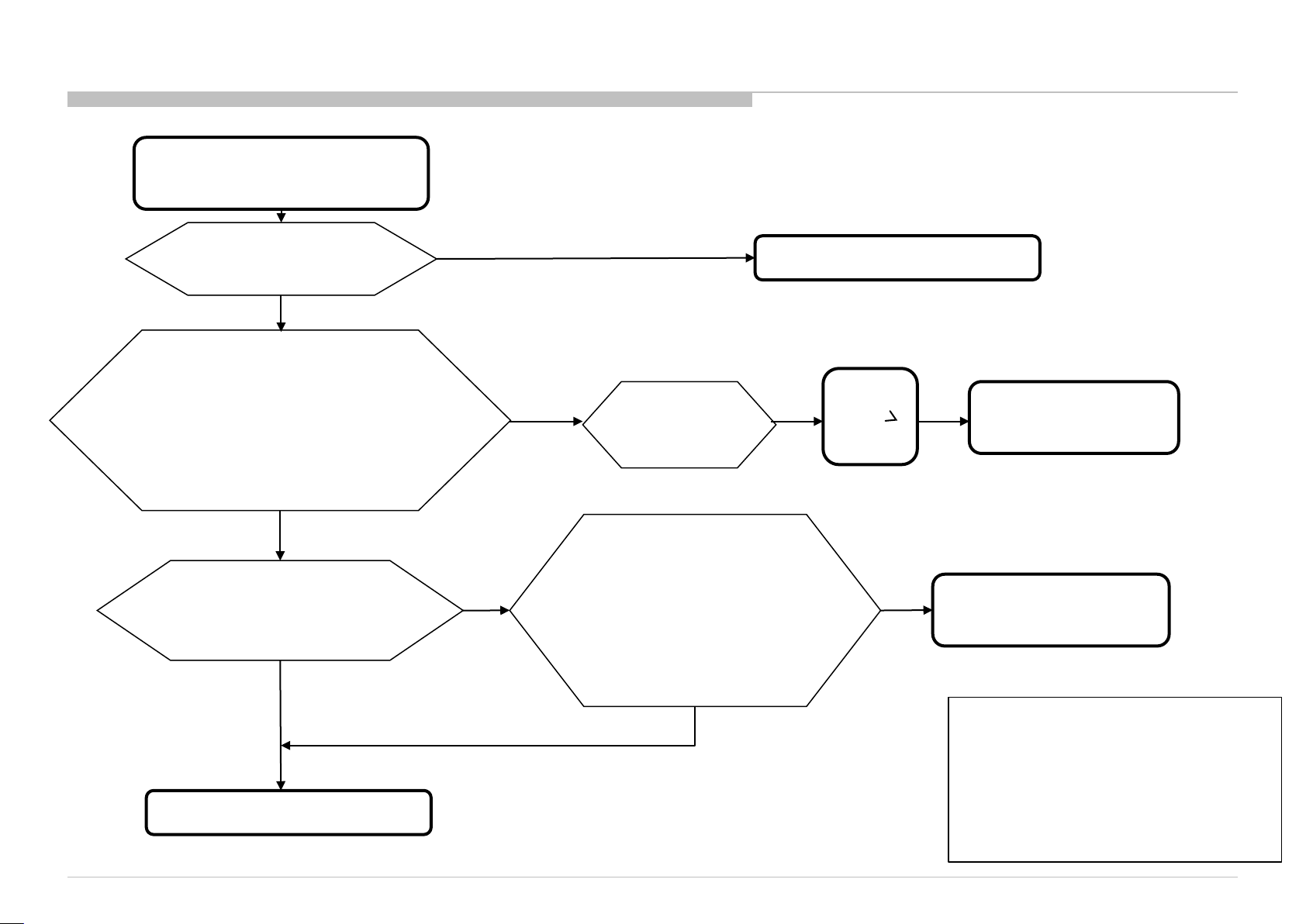
4.4 NO PICTURE: @ TUNER
RF input no picture / noisy
picture
Check RF source cable
and antenna, OK?
OK
Check Tuner power line:
3.3V at JL2800 = 3.3V?, R2865?
1.8V at JL2801 = 1.8V? , FB2803?
A_RESET value at JL2807 = 3.3V?
OK
All broadcasting channel
cannot be received?
NO
NG
YES
Change RF cable and antenna
NG
Check :
NG
R2865
FB2803
Check part mounting condition
for I2C SDA & SCL line (Refer Note I2C)
And
Check Tuner module connection (BFX)
Change
R2865
FB2803
NG
Please refer DDCON
troubleshooting
Change NG parts
connected to I2C bus
Refer to next page
OK
Notes:
I2C line for all tuners except Japan_SKP
- Parts for I2C SDA line: R2800, C2803.
- Parts for I2C SCL line : R2801, C2804.
I2C line for Japan_SKP
- Parts for I2C SDA line: R2804
- Parts for I2C SCL line : R2805
89
89
Page 90
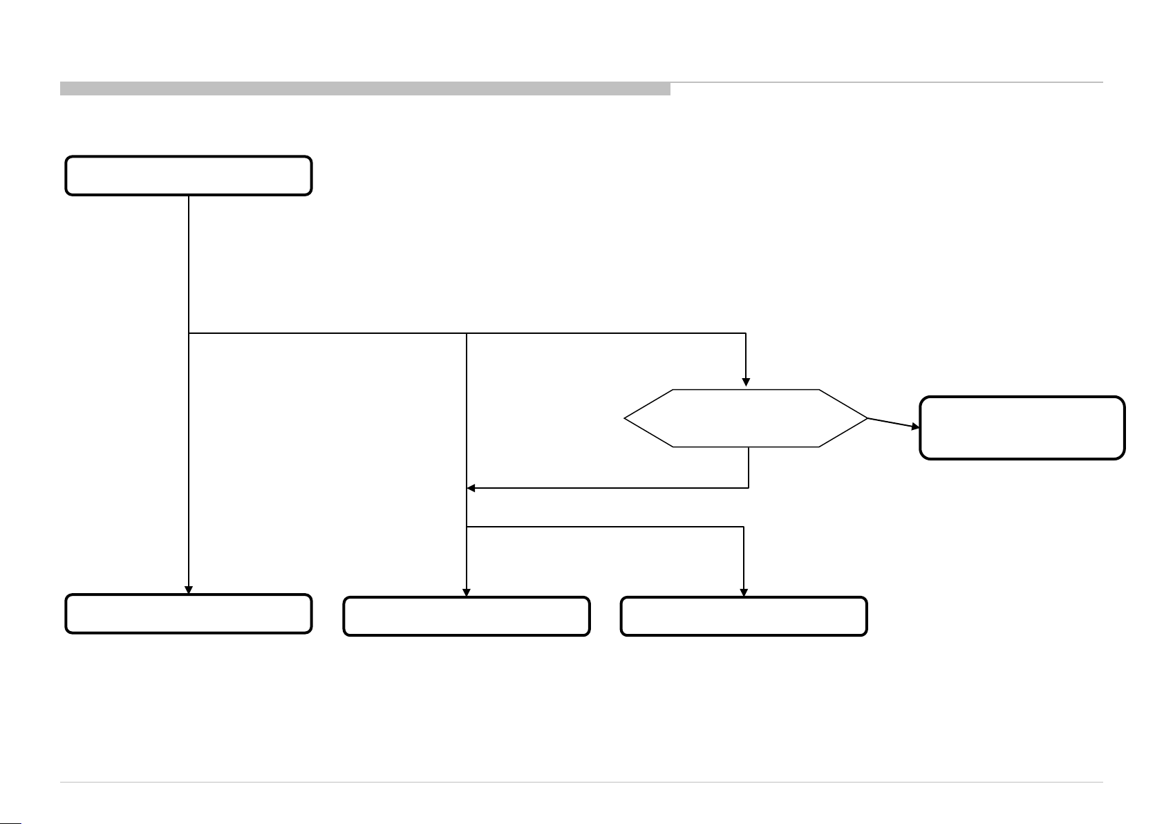
4.4 NO PICTURE: @ TUNER
From Previous page
Digital
Analog
Refer Analog Tuning
Terrestrial/Cable
For TW, NA-
ATSC(MX/UC),
JP_SKP(Opticast) and
LA-ISDB-T
Refer Digital Tuning 1
Satellite
Check Tuner power line
12V at JL2822 = 12V?
OK
For AEP_W, JP_SKP, PA_T2,
CH/HK, and LA-T2(COL)
Refer Digital Tuning 2
NG
12V LNB Voltage
Checking
90
Page 91
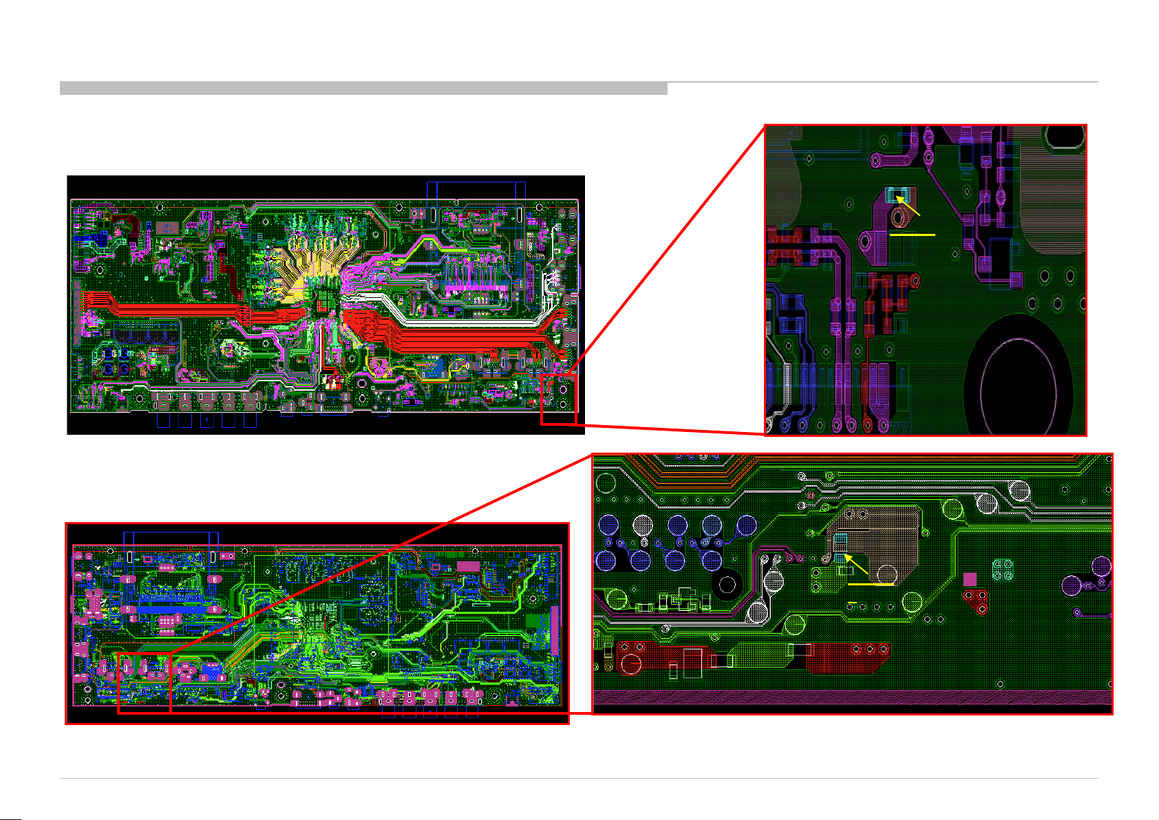
4.4 NO PICTURE: @ TUNER (BFX)
BFX (Top View)
For Tuner Power Lines
R2865
BFX (Back View)
For Tuner Power Lines
FB280
3
91
Page 92
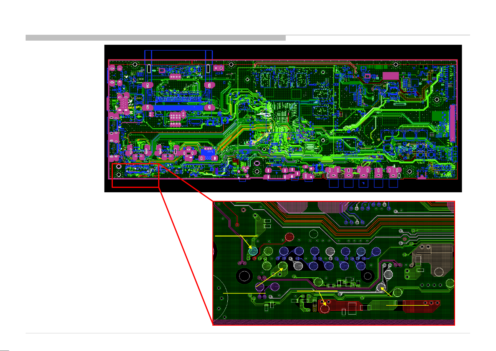
4.4 NO PICTURE: @ TUNER (BFX)
BFX (Back View)
For Tuner Power Lines
JL2800 = 3.3V
JL2801 = 1.8V
JL2822 = 12V
JL2807 = 3.3V
92
Page 93
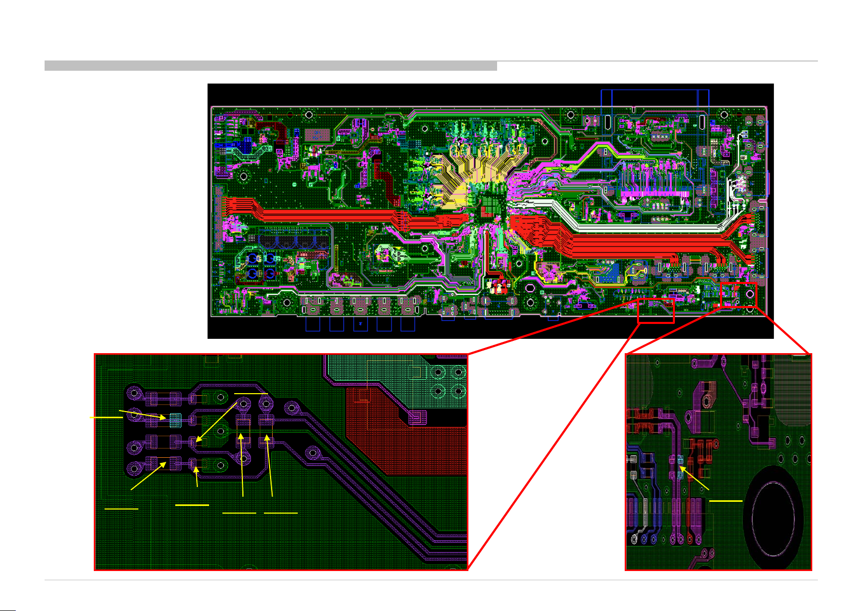
4.4 NO PICTURE: @ TUNER (BFX)
BFX (Top View)
For Tuner I2C line
R2802
R2801
C2804
C2803
R2806
R2804 R2805
93
Page 94
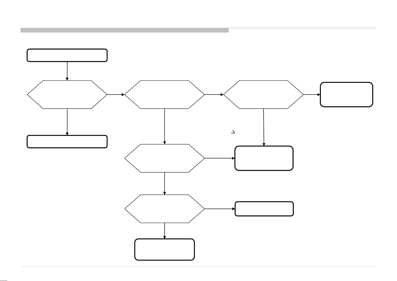
4.4 NO PICTURE: @ TUNER
FOR 12V LNB Voltage Checking: @ AEP_W and JP_SKP
12V LNB Voltage Checking
Check fuse F2800
NG
Change the fuse
OK
Check LNB power line
+12V_MAIN at R495 = 12V?
N
G
AC adapter or G-board
G-board
Check harness between
B-Board and G-board
OK
AC
adapter
NG
Check P_ON_LNB signal line
at R446 = 3.3V?
NG
Please refer
DDCON
troubleshooting
Harness broken
OK
MOSFET
Q408/Q409
broken
OK
Please refer G-board
troubleshooting
94
Page 95
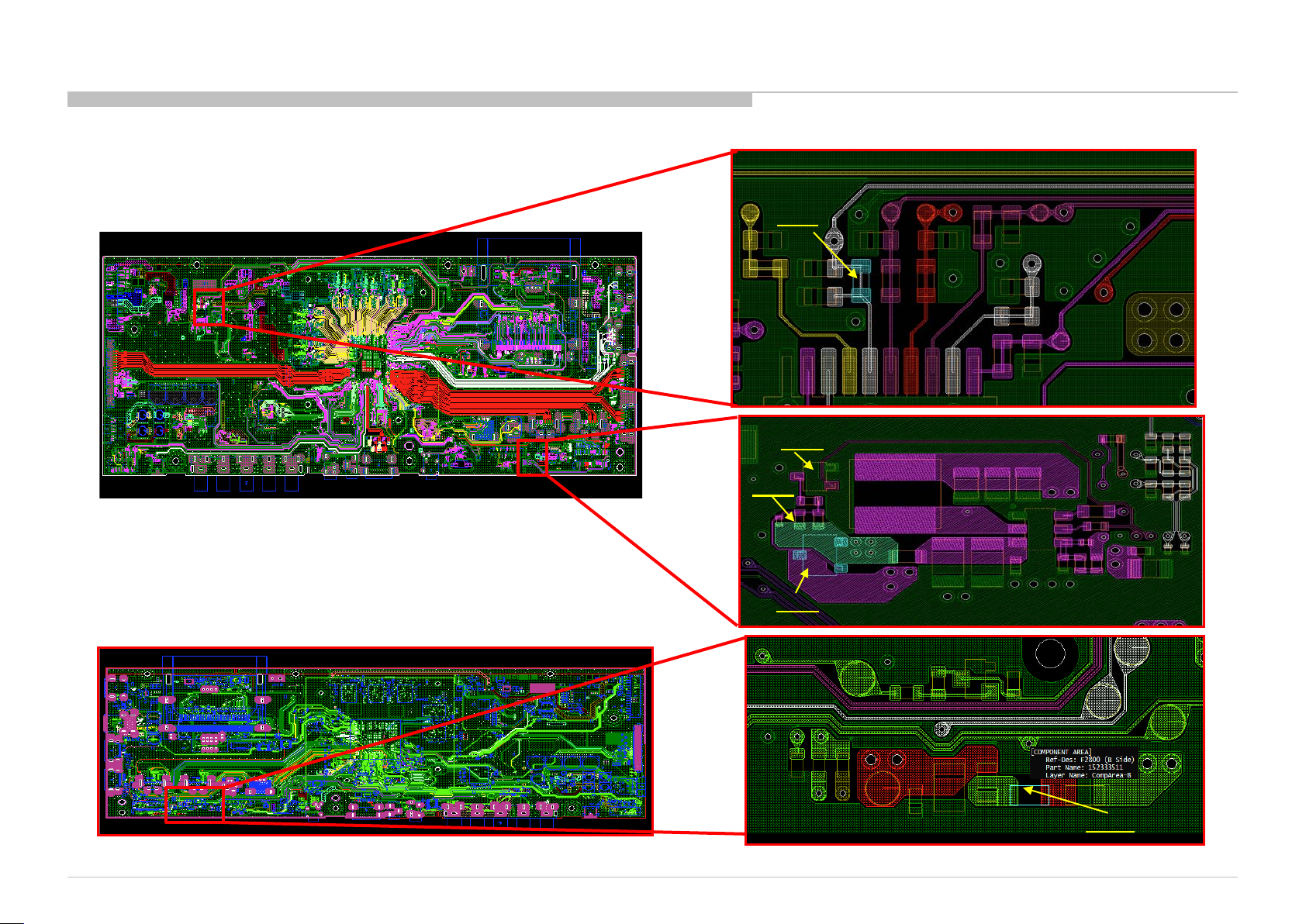
4.4 NO PICTURE: @ TUNER (BFX)
BFX (Top View)
12V LNB Voltage line
BFX (Back View)
12V LNB Voltage line
R446
Q408
R495
Q409
F2800
95
Page 96
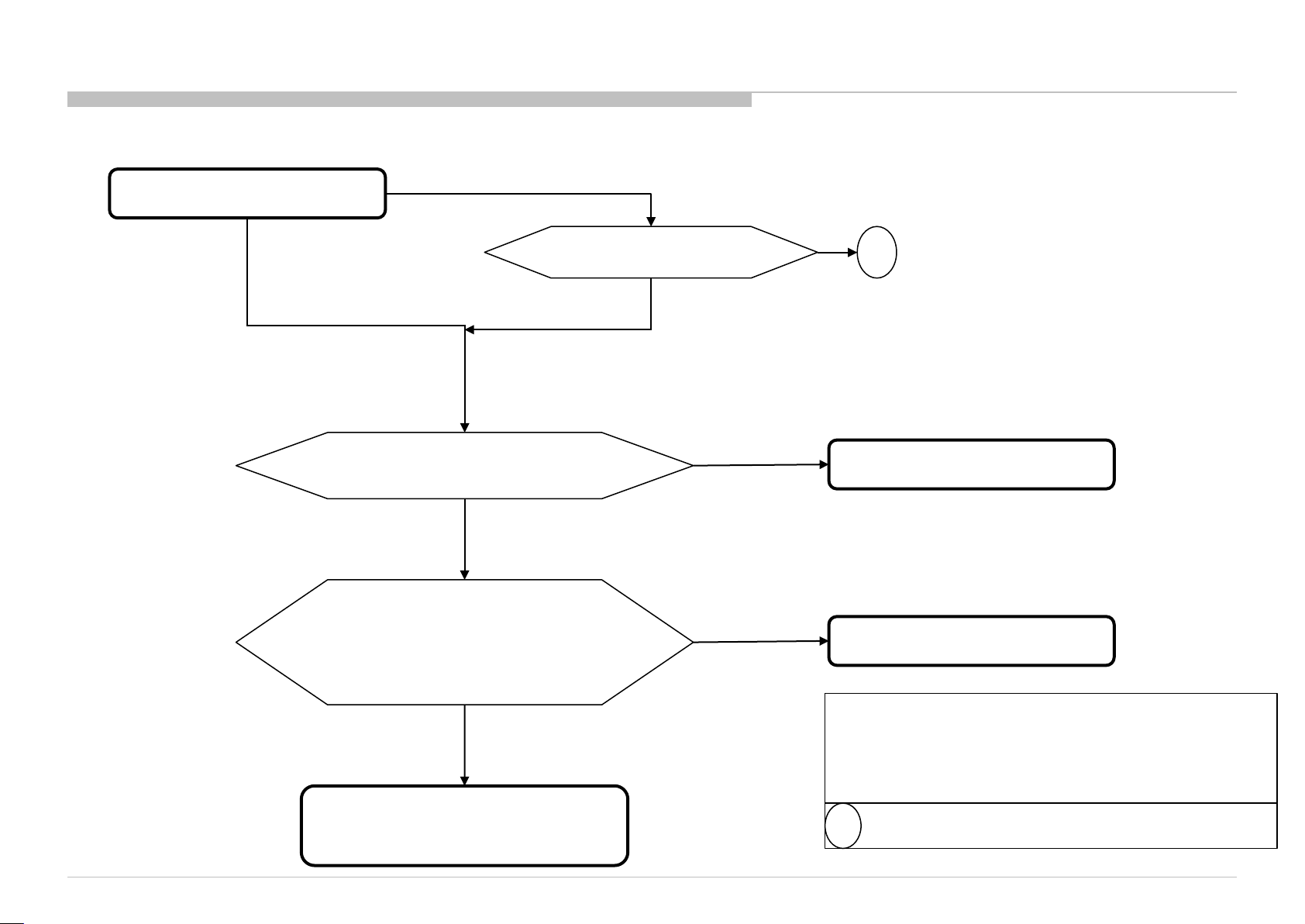
4.4 NO PICTURE: @ TUNER
FOR ANALOG TUNING: @ All destination except JP_SKP
For LA-ISDB(BR/AR), LA-T2(COL) and TW only
Analog Tuning
For Other destination
Confirm ANT or Cable connection A
Channel can be lock?
NG
Check part mounting condition
for analog control line
“IFOUT_N, IFOUT_P, IFAGC”
NG
OK
Check IC1000 (SoC)
OK
Change NG parts
NG
OK
Check IC1000 (SoC) &
Tuner module connection (BFX)
Notes:
- Parts for IFOUT_N line : FB2801, C2807, C2826
- Parts for IFOUT_P line : FB2802, C2808, C2825
- Parts for IFAGC line : R2838, C2827
: Insert correct signal in correct terminal.
A
96
Page 97
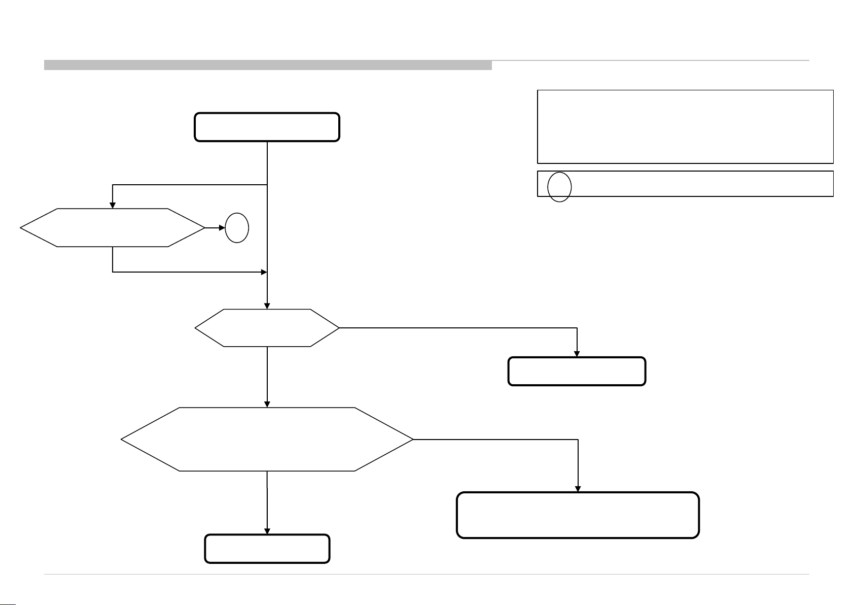
4.4 NO PICTURE: @ TUNER
FOR DIGITAL TUNING 1: @ TW, NA-ATSC(MX/UC), JP_SKP(Opticast) and LA-ISDB-T.
Digital Tuning 1
Notes:
- Parts for IFOUT_N line : FB2801, C2807, C2826
- Parts for IFOUT_P line : FB2802, C2808, C2825
- Parts for IFAGC line : R2838, C2827
For TW/LA-ISDB-T
Confirm ANT or Cable connection
Check part mounting condition
“IFOUT_N, IFOUT_P, IFAGC”
For NA-
NG
A
Sound is normal?
for digital data line
ATSC(MX/UC)/JP_SKP(Opticast)
No sound
OK
OK
: Insert correct signal in correct terminal.
A
Check IC1000 (SoC)
NG
Change NG parts
Check SoC(IC1000) and Tuner module
Check Tuner module connection (BFX)
97
Page 98
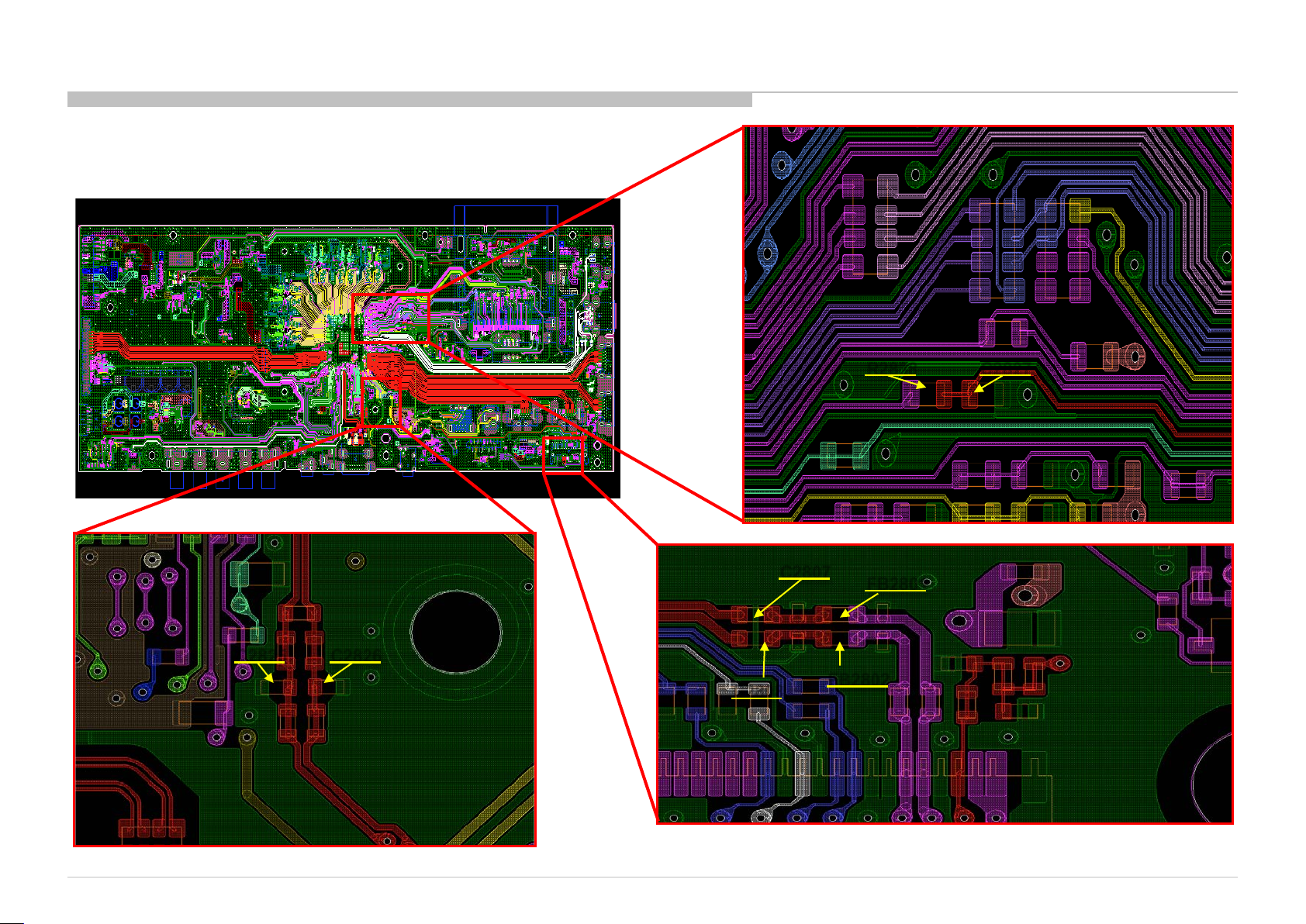
4.4 NO PICTURE: @ TUNER (BFX)
BFX (Top View)
IF & IFAGC line
R2838 C2827
C2825 C2826
C2808
C2807
FB2801
FB2802
98
Page 99
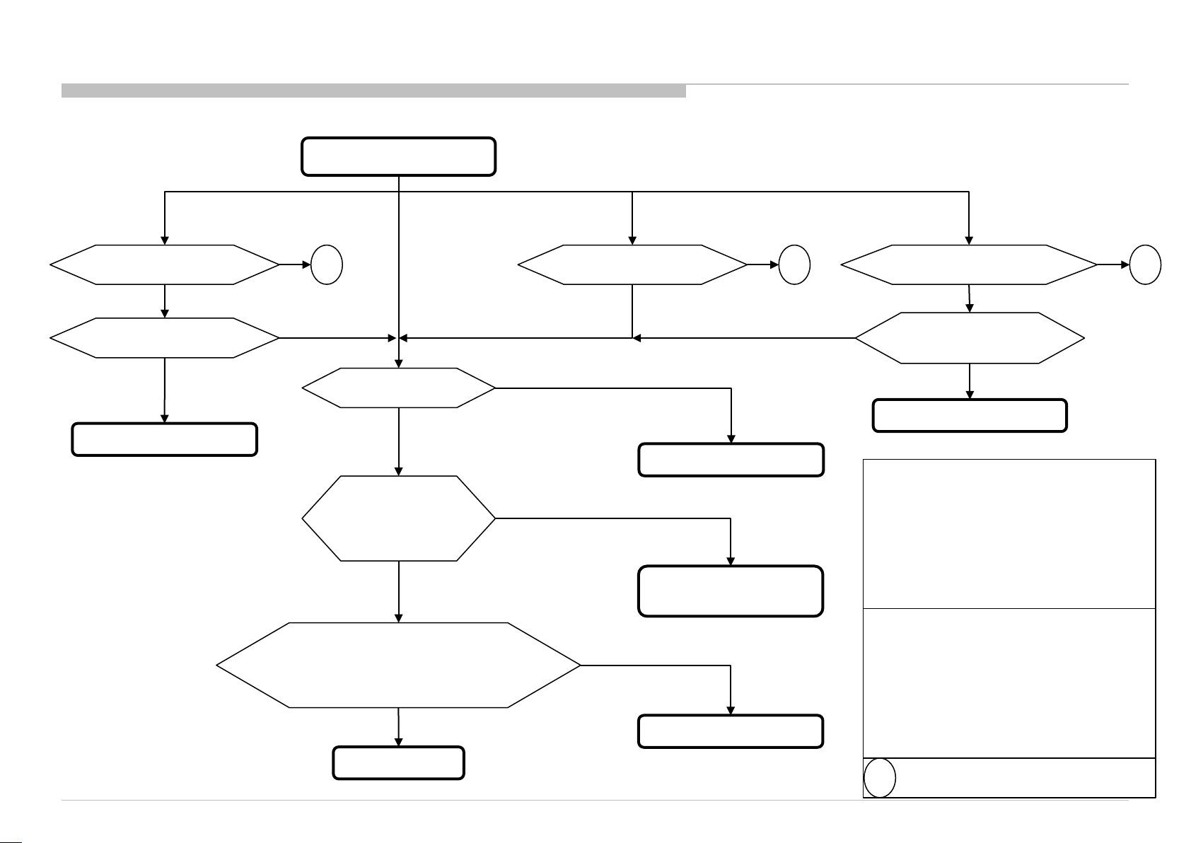
4.4 NO PICTURE: @ TUNER
FOR DIGITAL TUNING 2: @ AEP_W, JP_SKP, PA_T2, CH/HK, and LA-T2(COL)
Digital Tuning 2
LA-T2(COL) For AEP-W For PA_T2 and
CH/HK
NG
Confirm ANT or Cable connection Confirm ANT or Satellite connection
OK
Digital cable/ Terrestrial
Cable
Refer to Digital Tuning 1
A A A
OK
Terrestrial
OK
Sound is normal?
No sound
Check IC1000 (SoC)
On Service
mode display
TS_LOCK ?
UEC ?
CASE A
CASE B
Change Tuner module
(Refer to Note tuner )
For JP_SKP
NG NG
Confirm ANT or Satellite connection
OK
All except SKP_Opticast
BS/CS or SKP_Opticast/
SKP_Premium or terrestrial
SKP_Opticast
Refer to Digital Tuning 1
Notes:
- Parts for TU1_TS_DATA0 line : R2847.
- Parts for TU1_TS_CLK line : R2844, R2815,R2866
- Parts for TU1_TS_VALID line : R2845.
- Parts for TU1_TS_SYNC line : R2846.
- CASE A : TS _LOCK = LOCK and UEC constant
- CASE B : TS _LOCK = UNLOCK or UEC is increasing
Check part mounting condition for digital data line
“TU1_TS_DATA0, TU1_TS_CLK,
TU1_TS_VALID, TU1_TS_SYNC”
NG
Change NG parts
OK
Check IC1000 (SoC)
Note (Only BM2 PWB)
(Tuner reference -- destination)
TU2801 - PA-T2
TU2801 - LA-T2(COL)
TU2801 - CH, HK
TU2803 - AEP_W
TU2802 - JP_SKP
: Insert correct signal in correct terminal.
A
99
Page 100
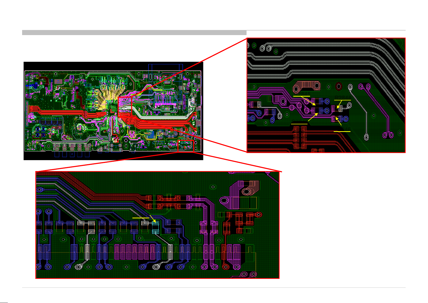
4.4 NO PICTURE: @ TUNER (BFX)
BFX (Top View)
TS1 line
R2815
R2845
R2847
R2844
R2846
100
100
 Loading...