

Sony ILX521A Datasheet

ILX521A
256-pixel CCD Linear Image Sensor (B/W)
Description
The ILX521A is a rectangular reduction type CCD
linear image sensor designed for image scanner
sensor. A built-in timing generator and clock driver
ensure single 5V power supply for easy use.
Features
• Number of effective pixels: 256 pixels
• Pixel size: 14µm × 14µm (14µm pitch)
• Built-in timing generator and clock driver
• Built-in S/H circuit
• Maximum data rate: 2MHz
• Single 5V power supply
• Clear mold package (12-pin SDIP)
Absolute Maximum Ratings
• Supply voltage VDD 6V
•Operating temperature –10 to +60 °C
• Storage temperature –30 to +80 °C
Pin Configuration (Top View)
Block Diagram
– 1 –
E99154-PS
Sony reserves the right to change products and specifications without prior notice. This information does not convey any license by
any implication or otherwise under any patents or other right. Application circuits shown, if any, are typical examples illustrating the
operation of the devices. Sony cannot assume responsibility for any problems arising out of the use of these circuits.
12
11
10
9
8
7
1
2
3
4
5
6
GND
V
OUT
TEST
φCLK
S/H SW
φROG
NC
NC
NC
NC
V
DD
NC
1
256
TEST GNDVOUT VDD S/H SW
Readout gate
CCD analog shift register
Clock driver
Mode selector
ROG pulse
generator
Clock pulse generator
42 1 8 65
φROGφCLK
D7
D8
D12
S1
S2
S255
S256
D13
D17
3
• Output amplifier
• S/H circuit
12 pin SDIP (MOLD)

– 2 –
ILX521A
Pin Description
Pin No. Symbol Description
1
2
3
4
5
6
7
8
9
10
11
12
GND
VOUT
TEST
φCLK
S/H SW
φROG
NC
VDD
NC
NC
NC
NC
GND
Signal output
Test (open)
Clock pulse input
Switching of with S/H or without S/H
Readout gate pulse input
NC
5V power supply
NC
NC
NC
NC
Input Pin Capacity
CφCLK
CφROG
Min.
—
—
Typ.
10
10
Max.
—
—
Unit
pF
pF
Item Symbol
Input capacity of φCLK pin
Input capacity of φROG pin
Input Clock Voltage Condition
∗1
High level
Low level
Min.
Symbol
4.5
0
VIH
VIL
Typ.
VDD
—
Max.
VDD + 0.5
0.5
Unit
V
V
Item
∗1
This is applied to the all external pulses. (φCLK, φROG)
Mode Description
Used mode
with S/H
without S/H
Pin 5 S/H SW
GND
VDD
Recommended Voltage
Item
VDD
Min.
4.75
Typ.
5.0
Max.
5.25
Unit
V
– 3 –
ILX521A
Electrooptical Characteristics
(Ta = 25°C, VDD = 5V, Data rate = 1MHz, Without S/H mode, Light source = 3200K,
IR cut filter CM-500S (t = 1mm))
Item Symbol Min. Typ. Max. Unit Remarks
Sensitivity
Sensitivity nonuniformity
Saturation output voltage
Dark voltage average
Dark signal nonuniformity
Image lag
Dynamic range
Saturation exposure
Current consumption
Total transfer efficiency
Output impedance
Offset level
R
PRNU
VSAT
VDRK
DSNU
IL
DR
SE
IVDD
TTE
ZO
VOS
13.3
—
0.6
—
—
—
—
—
—
92.0
—
—
19.0
5.0
0.8
0.3
0.5
0.02
2666
0.042
5.0
98.0
350
3.8
24.7
12.0
—
2.0
3.0
—
—
—
10.0
—
—
—
V/(lx · s)
%
V
mV
mV
%
lx · s
mA
%
Ω
V
Note 1
Note 2
—
Note 3
Note 3
Note 4
Note 5
Note 6
—
—
—
Note 7
Note)
1. For the sensitivity test light is applied with a uniform intensity of illumination.
2. PRNU is defined as indicated below. Ray incidence conditions are the same as for Note 1.
PRNU = × 100 [%]
The maximum output of the 256 pixels is set to VMAX, the minimum output to VMIN and the average output to
VAVE.
3. Integration time is 10ms.
4. VOUT = 500mV.
5. DR = VSAT/VDRK
When optical integration time is shorter, the dynamic range sets wider because dark output voltage is in
proportion to optical integration time.
6. SE = VSAT/R1
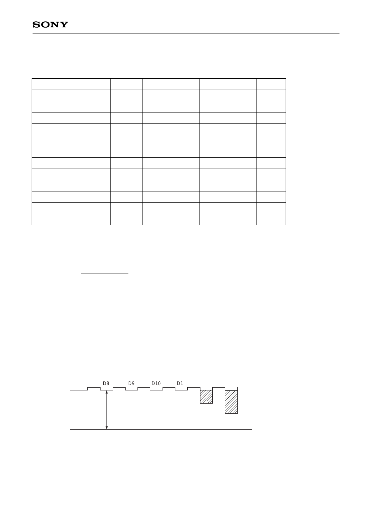
7. Vos is defined as indicated below.
(VMAX – VMIN)/2
VAVE
,
D8 D9 D10 D11 D12 S1
Vout
V
OS
GND

– 4 –
ILX521A
φROG
φCLK
VOUT
0V
5V
5V
0V
21 3 6 7 8 9 10 11 12 13 14
268
269
270
271
272
273
1
D1
D2
D3
D6
Optical black
(4 pixels)
Effective pixel
signal
(256 pixels)
Dummy signal
(5 pixels)
Dummy signal (12 pixels)
1-line output period (273 pixels)
Note) 280 or more clock pulses are required.
D7
D8
D9
D10
D11
D12
S1
S2
S256
D13
D14
D15
D16
D17
Clock Timing Diagram (without internal S/H mode)
 Loading...