

Sony ILX511 Datasheet
2048-pixel CCD Linear Image Sensor (B/W)
For the availability of this product, please contact the sales office.
Description
The ILX511 is a rectangular reduction type CCD
linear image sensor designed for bar code POS
hand scanner and optical measuring equipment use.
A built-in timing generator and clock-drivers ensure
single 5 V power supply for easy use.
Features
• Number of effective pixels: 2048 pixels
• Pixel size: 14 µm × 200 µm
(14 µm pitch)
• Single 5 V power supply
• Ultra-high sensitivity
• Built-in timing generator and clock-drivers
• Built-in sample-and-hold circuit
• Maximum clock frequency: 2MHz
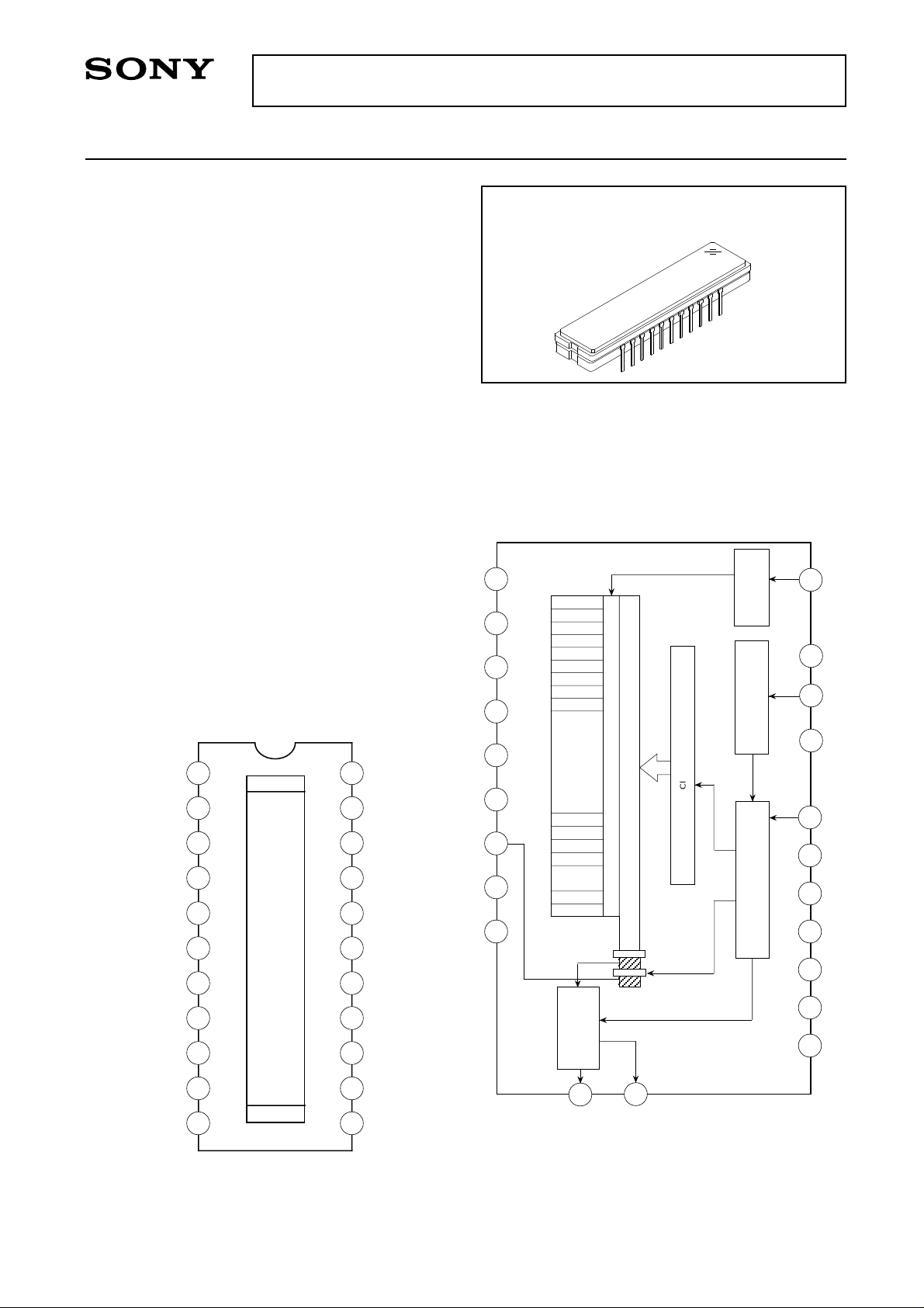
Block Diagram
ILX511
22 pin DIP (Plastic)
Absolute Maximum Ratings
• Supply voltage VDD 6V
•Operating temperature –10 to +60 °C
• Storage temperature –30 to +80 °C
NC NC GND
Pin Configuration (Top View)
OUT
V
GND
GND
SHSW
φCLK
V
NC
NC
1
2
3
4
5
6
DD
7
8
1
22
21
20
19
18
17
16
15
VDD
VDD
VDD
GND
V
GG
GND
GND
DD
V
DD
GND GND V
DD
V
DD
V
DD
V
12
13
14
15
16
17
20
21
22
D38
D37
D36
D35
D34
D33
S2048
S2047
S2046
Readout gate
CCD analog shift register
S3
S2
S1
D32
D14
D13
Clock-drivers
11
φROG
pulse generator
Readout gate
19
GND
4
10
5
9
8
7
6
3
SHSW
NC
φCLK
DD
V
NCNCV
DD
GNDGND
Mode selector
Sample-and-hold pulse generator
Clock plse generator/
NC
V
NC
φROG
9
DD
10
11
2048
14
13
12
NC
GND
S/H circuit
Output amplifier
Internal Structure
1
OUT
V
GG
V
18
Sony reserves the right to change products and specifications without prior notice. This information does not convey any license by
any implication or otherwise under any patents or other right. Application circuits shown, if any, are typical examples illustrating the
operation of the devices. Sony cannot assume responsibility for any problems arising out of the use of these circuits.
—1—
2
E94108-TE
Pin Description
ILX511
Pin No.
1
2
3
4
5
6
7
8
9
10
11
12
13
14
15
16
17
18
19
20
21
22
Symbol
VOUT
GND
GND
SHSW
φ
CLK
VDD
NC
NC
VDD
NC
φ
ROG
GND
NC
NC
VDD
GND
GND
VGG
GND
VDD
VDD
VDD
Description
Signal output
GND
GND
Switch (with S/H or without S/H)
Clock pulse input
5V power supply
NC
NC
5V power supply
NC
Readout gate pulse input
GND
NC
NC
5V power supply
GND
GND
Output circuit gate bias
GND
5V power supply
5V power supply
5V power supply
Mode Description
Mode in Use Pin 4 (SHSW)
With S/H GND
Without S/H VDD
Recommended Voltage
Item Min. Typ. Max. Unit
VDD 4.5 5.0 5.5 V
Input Clock Voltage Condition (Note)
Item Min. Typ. Max. Unit
VIH 4.5 5.0 5.5 V
VIL 0 — 0.5 V
Note) This is applied to the all pulses applied externally. (φ CLK, φ ROG)
Item Symbol Min. Typ. Max. Unit
Input capacity of φ CLK pin C
φ
CLK —10— pF
—2—
ILX511
Electro-optical Characteristics
(Ta = 25 °C, VDD = 5 V, Clock frequency: 1 MHz, Light source = 3200 K, IR cut filter: CM-500S (t = 1.0 mm),
Without S/H mode)
Item Symbol Min. Typ. Max. Unit Remarks
Sensitivity 1
Sensitivity 2
Sensitivity nonuniformity
Saturation output voltage
Dark voltage average
Dark signal nonuniformity
Image lag
Dynamic range
Saturation exposure
5 V current consumption
Total transfer efficiency
Output impedance
Offset level
R1 150 200 250 V/(lx • s)
R2 — 1800 — V/(lx • s)
PRNU — 5.0 10.0 %
VSAT 0.6 0.8 — V
VDRK — 3.0 6.0 mV
DSNU — 6.0 12.0 mV
IL — 1 — %
DR — 267 — —
SE — 0.004 — lx • s
I VDD — 5.0 10.0 mA
TTE 92.0 98.0 — %
ZO — 250 — Ω
VOS — 2.8 — V
Note 1
Note 2
Note 3
—
Note 4
Note 4
Note 5
Note 6
Note 7
—
—
—
Note 8
Note)
1. For the sensitivity test light is applied with a uniform intensity of illumination.
2. Light source: LED λ = 660nm
3. PRNU is defined as indicated below. Ray incidence conditions are the same as for Note 1.
PRNU =
(VMAX-VMIN)/2
VAVE
× 100 (%)
The maximum output of all the valid pixels is set to VMAX, the minimum output to VMIN and the average
output to VAVE.
4. Integration time is 10ms.
5. Typical value is used for clock pulse and readout pulse. VOUT = 500 mV.
6. DR = VSAT/VDRK. When optical integration time is shorter, the dynamic range sets wider because dark
voltage is in proportion to optical integration time.
7. SE = VSAT/R1
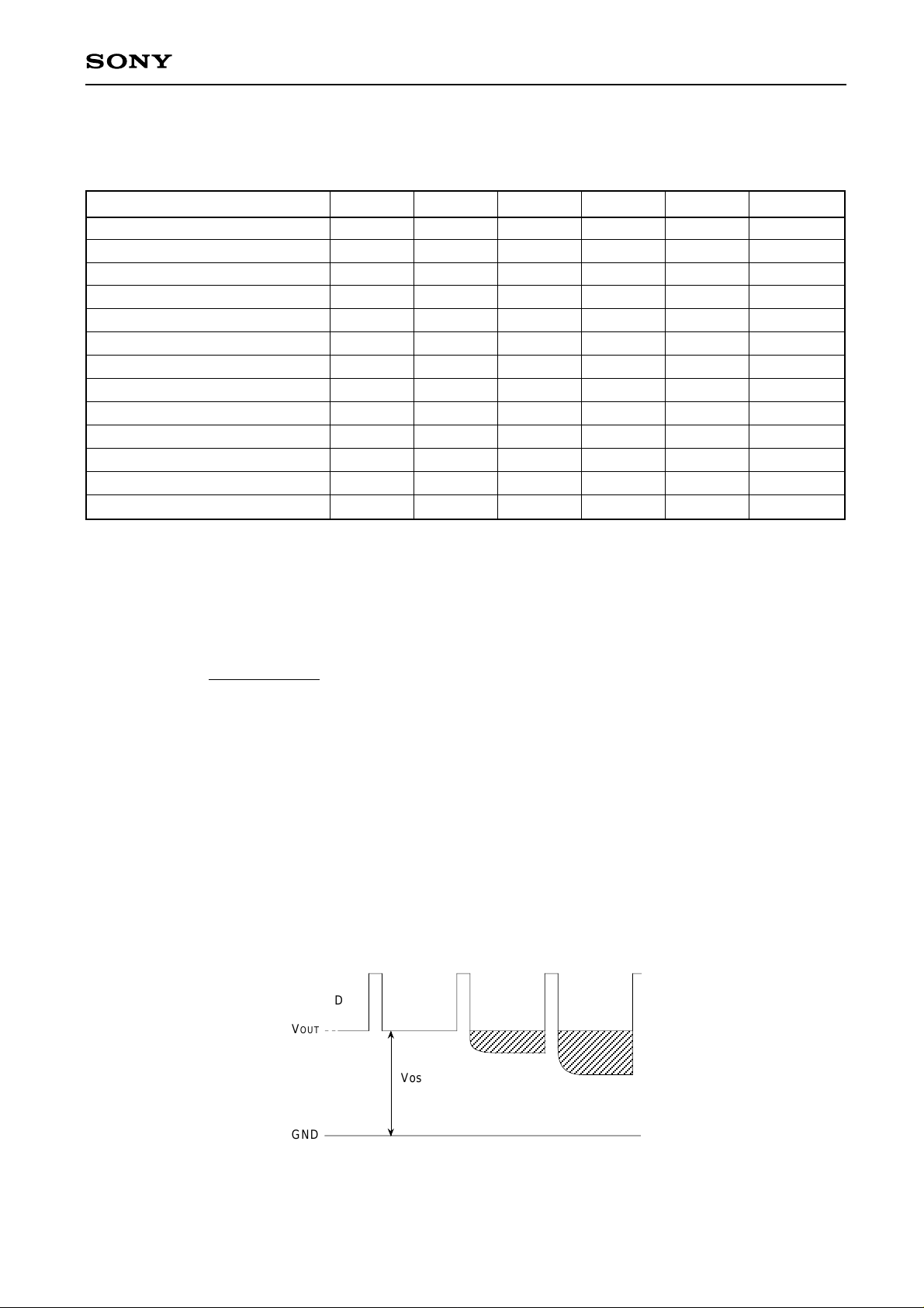
8. Vos is defined as indicated below.
D30 D31 D32 S1
V
OUT
GND
Vos
—3—
ILX511
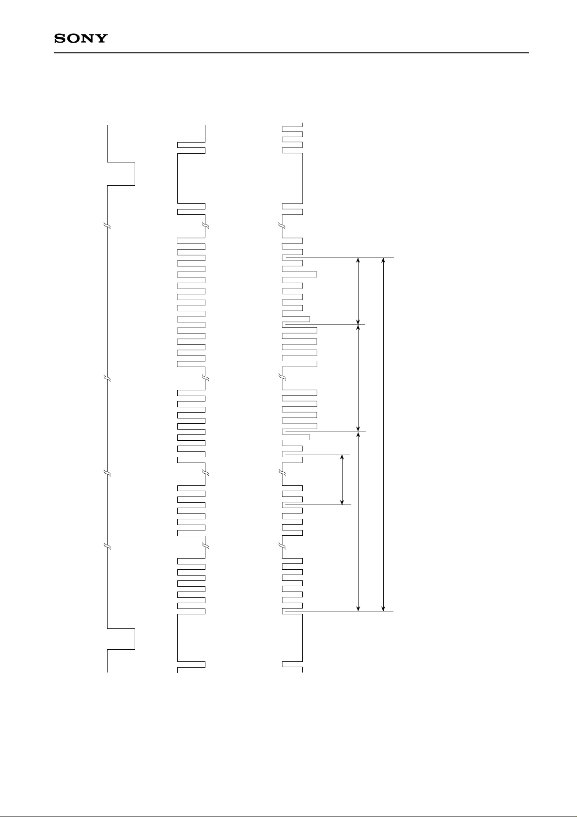
1
2086
D38
D37
D36
D35
D34
D33
S2048
S2047
S2046
S2045
S4
S3
S2
S1
D32
D31
D30
D14
D13
D12
D11
D10
(6 pixels)
Dummy signal
signal (2048 pixels)
Effective picture elements
1-line output period (2086 pixels)
(18 pixels)
Optical black
)
DD
∗ Without S/H mode (4pin Æ V
2088 or more clock pulses are required.
3
2
1
0
5
Clock Timing Diagram (Without S/H mode)
φROG
0
5
φCLK
D5
D4
D3
D2
D1
∗
—4—
OUT
V
Dummy signal (32 pixels)
 Loading...