

Sony ILX506 Datasheet
5000-pixel CCD Linear Image Sensor (B/W)
For the availability of this product, please contact the sales office.
Description
The ILX506 is a reduction type CCD linear sensor
developed for high resolution facsimiles and copiers.
This sensor reads A3-size documents at a density of
400 DPI (Dot Per Inch). A built-in timing generator
and clock-drivers ensure direct drive at 5V logic for
easy use. In addition, reset pulse can be switched
between internal generation and external input.
Features
• Number of effective pixels: 5000 pixels
• Pixel size: 7µm × 7µm (7µm pitch)
• Built-in timing generator and clock-drivers
• Ultra low lag/ultra high sensitivity/low dark output
• Single output method
• Maximum clock frequency: 12.5MHz
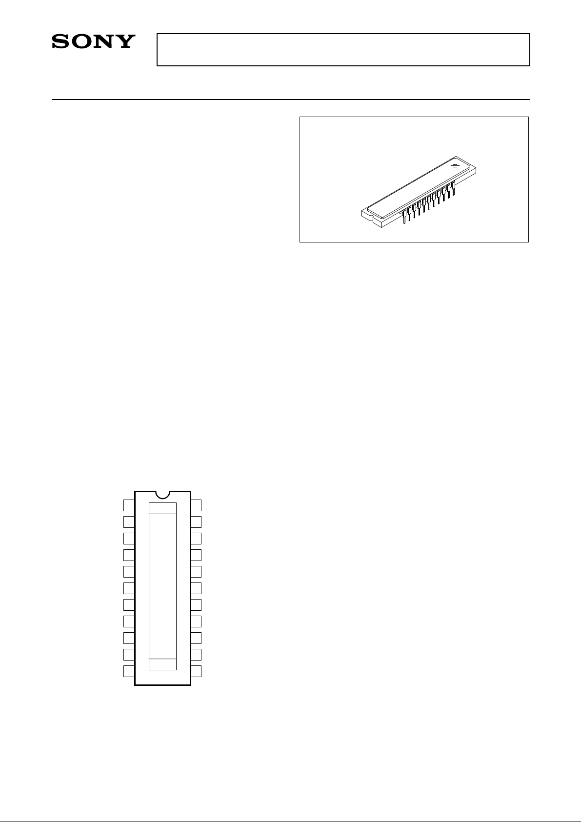
ILX506
22 pin DIP (Ceramic)
Absolute Maximum Ratings
• Supply voltage VDD1 11 V
VDD2 6V
•Operating temperature –10 to +60 °C
• Storage temperature –30 to +80 °C
Pin Configuration (Top View)
GG
V
GND
V
DD1
VOUT
GND
φROG
V
DD2
VDD2
RSSW
T1
GND
10
11
1
2
3
4
5
6
7
8
9
1
5000
22
21
20
19
18
17
16
15
14
13
12
φCLK
VDD1
RS/SH
V
DD1
VDD1
GND
V
DD2
GND
T4
T3
T2
Sony reserves the right to change products and specifications without prior notice. This information does not convey any license by
any implication or otherwise under any patents or other right. Application circuits shown, if any, are typical examples illustrating the
operation of the devices. Sony cannot assume responsibility for any problems arising out of the use of these circuits.
– 1 –
E92239B78-PS
ILX506
DD2
DD1
DD1
DD1
T2
T3
T4
GND
V
GND
V
V
V
12
13
1415
16
17
18
19
21
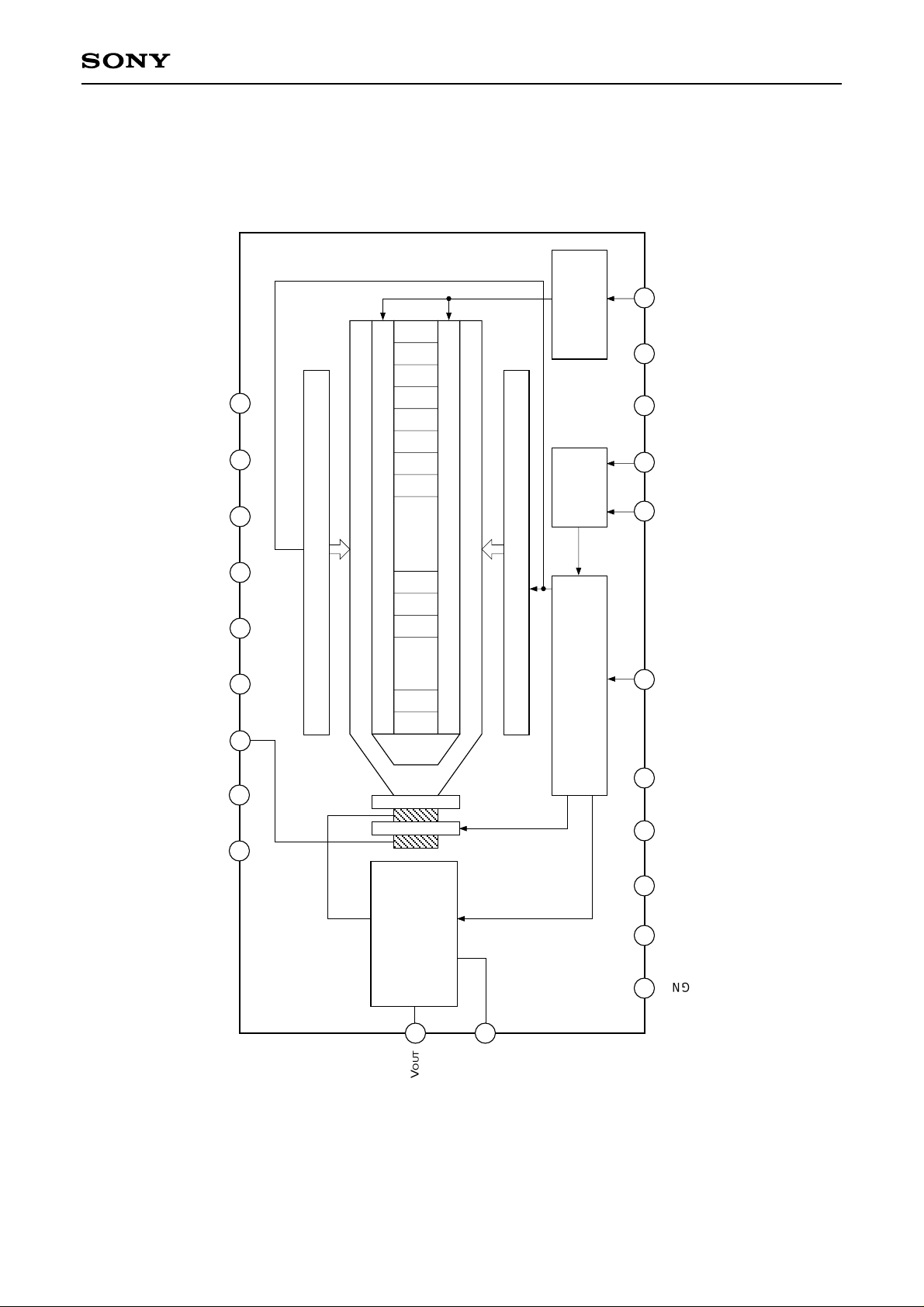
Clock-drivers
Read out gate
CCD analog shift register
.
D34
D33
D32
D31
D30
D29
S5000
S4999
Read out gate
S2
S1
D28
D18
D17
Read out gate
pulse generator
Mode
selector
Clock-drivers
CCD analog shift register
Clock pulse generator
Sample-and-hold pulse generator
6
11
10
20
9
22
8
7
5
T1
DD2
DD2
φROG
GND
RS/SH
RSSW
φCLK
V
V
GND
Block Diagram
• Output amplifier
• Sample-and-hold circuit
• Feed through
suppression circuit
4
VOUT
1
VGG
– 2 –
V
DD1
3
GND
2
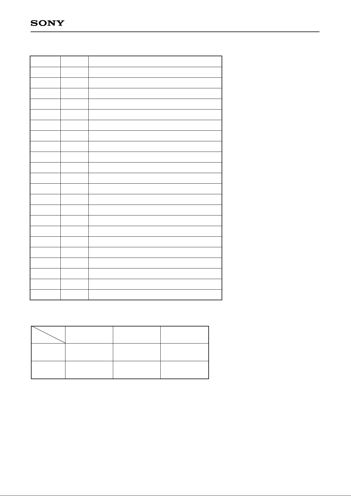
Pin Description
ILX506
Pin No.
1
2
3
4
5
6
7
8
9
10
11
12
13
14
15
16
Symbol
VGG
GND
VDD1
VOUT
GND
φROG
VDD2
VDD2
RSSW
T1
GND
T2
T3
T4
GND
VDD2
Output circuit gate bias
GND
9V power supply
Signal output
GND
Clock pulse
5V power supply
5V power supply
∗1
Reset pulse switchover pin
Test pin (5V)
GND
Test pin (GND)
Test pin (5V)
Test pin (GND)
GND
5V power supply
Description
17
18
19
20
21
22
∗1
Output mode is changeable as follows.
9pin
GND
VDD1
20pin
GND
VDD1
VDD1
RS/SH
VDD1
φCLK
Internal RS
without S/H
GND
9V power supply
9V power supply
∗1
Clock pulse or with S/H; without S/H switch
9V power supply
Clock pulse
GND
—
VDD1
Internal RS
with S/H
—
φRS
—
External RS
without S/H
– 3 –
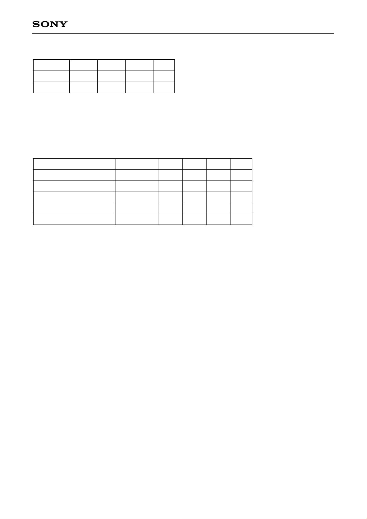
Recommended Voltage
ILX506
Item
VDD1
VDD2
Min.
8.5
4.75
Typ.
9.0
5.0
Max.
9.5
5.25
Unit
V
V
Note) Rules for raising and lowering power supply voltage
To raise power supply voltage, first raise VDD1 (9V) and then VDD2 (5V).
To lower voltage, first lower VDD2 (5V) and then VDD1 (9V).
Clock Characteristics
Item
Input capacity of φCLK pin
Input capacity of φROG pin
Input capacity of RS/SH pin
Frequency of φCLK
Frequency of φRS
Symbol
CφCLK
CφROG
CRS/SH
fφCLK
fφRS
Min.
—
—
—
—
—
Typ.
10
10
10
1
1
Max.
—
—
—
12.5
12.5
Unit
pF
pF
pF
MHz
MHz
– 4 –
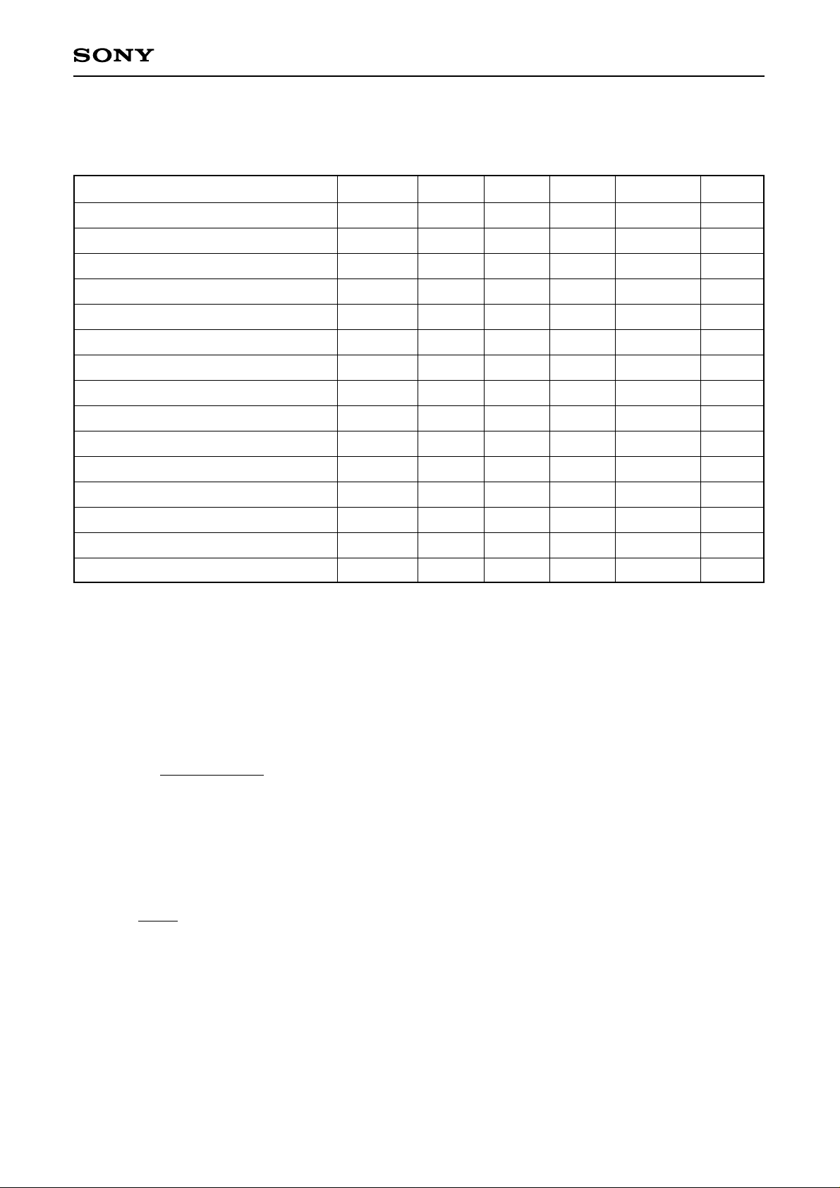
Electro-optical Characteristics (Note 1)
(Ta = 25°C, VDD1 = 9V, VDD2 = 5V, φCLK = 1MHz, Internal φRS mode without S/H,
ILX506
Light source = 3200K, IR cut filter, CM-500S (t = 1.0mm))
Item
Sensitivity 1
Sensitivity 2
Sensitivity nonuniformity
Saturation output voltage
Saturation exposure
Even and odd black level DC difference
Dark voltage average
Dark signal nonuniformity
Image lag
9V supply current
5V supply current
Total transfer efficiency
Output impedance
Offset level
Dynamic range
Symbol
R1
R2
PRNU
VSAT
SE
∆V
VDRK
DSNU
IL
IVDD1
IVDD2
TTE
ZO
VOS
DR
Min.
7.5
—
—
1.0
0.072
—
—
—
—
—
—
92
—
—
500
Typ.
10.8
24.6
4
1.5
0.139
1.0
0.3
0.6
0.02
16
3
98
600
3.0
5000
Max.
13.9
—
10
—
—
10.0
2
3
—
32
7
—
—
—
—
Unit
V/(lx · s)
V/(lx · s)
%
V
lx · s
mV
mV
mV
%
mA
mA
%
Ω
V
—
Remarks
Note 2
Note 3
Note 4
Note 5
Note 6
Note 7
Note 8
Note 9
Note 10
—
—
—
—
Note 11
Note 12
Notes)
1) In accordance with the given electrooptical characteristics, the even black level is defined as the mean
value of D8, D10, D12 to D14.
The odd black level is defined as the mean value of D7 , D9, D11 and D13.
2) For the sensitivity test light is applied with a uniform intensity of illumination.
3) W lamp (2854K)
4) PRNU is defined as indicated below. Ray incidence conditions are the same as for Note 2.
PRNU = × 100 [%]
(VMAX – VMIN)/2
VAVE
Where the 5000 pixels are divided into blocks of 100, even and odd pixels, respectively. The maximum
output of each block is set to VMAX, the minimum output to VMIN and the average output to VAVE.
5) Use below the minimum value of the saturation output voltage.
6) Saturation exposure is defined as follows.
SE =
VSAT
R1
7) Indicates the DC difference in value between odd black level and even black level.
8) Optical signal accumulated time τ int stands at 10ms.
– 5 –
 Loading...