

Sony ILX505A Datasheet
2592-pixel CCD Linear Image Sensor (B/W)
For the availability of this product, please contact the sales office.
Description
The ILX505A is a reduction type CCD linear sensor
designed for facsimile, image scanner and OCR use.
This sensor reads A3 size documents at a density of
200 DPI (Dot Per Inch). A built-in timing generator
and clock-drivers ensure direct drive at 5V logic for
easy use.
Features
• Number of effective pixels: 2592 pixels
• Pixel size: 11µm × 11µm (11µm pitch)
• Built-in timing generator and clock-drivers
• Ultra low lag
• High sensitivity
• Maximum clock frequency: 5MHz
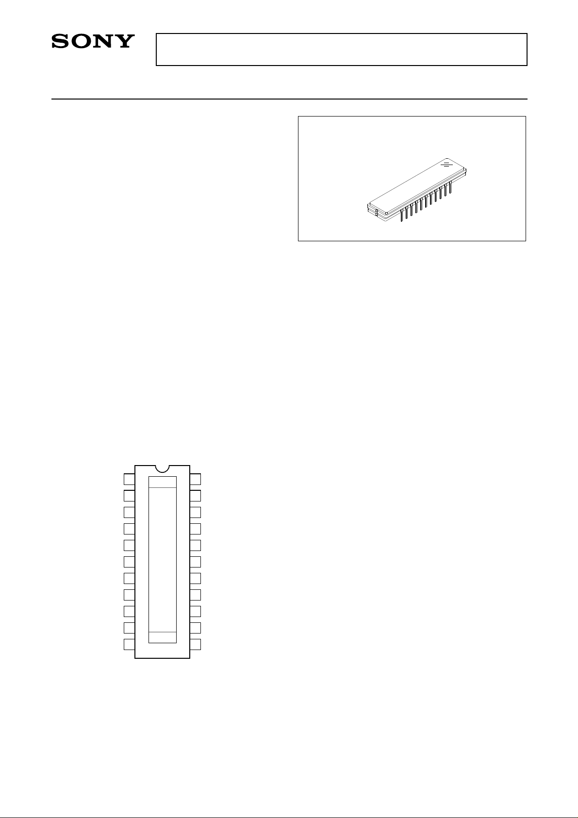
ILX505A
22 pin DIP (Ceramic)
Absolute Maximum Ratings
• Supply voltage VDD1 11 V
VDD2 6V
•Operating temperature –10 to +55 °C
• Storage temperature –30 to +80 °C
Pin Configuration (Top View)
OUT
V
GND
GND
SHSW
φCLK
DD1
V
GND
DD2
V
T1
EXRS
φROG
10
11
1
2
3
4
5
6
7
8
9
1
2592
22
21
20
19
18
17
16
15
14
13
12
DD2
V
NC
VDD1
RSSW
VGG
GND
GND
VDD1
NC
NC
GND
Sony reserves the right to change products and specifications without prior notice. This information does not convey any license by
any implication or otherwise under any patents or other right. Application circuits shown, if any, are typical examples illustrating the
operation of the devices. Sony cannot assume responsibility for any problems arising out of the use of these circuits.
– 1 –
E92Y22D78-PS
ILX505A
DD1
DD1
GND
NC
NC
V
GND
GND
V
12
13
1415
16
17
20
D39
D38
D37
D36
D35
D34
S2592
S2591
S2
S1
D33
D15
D14
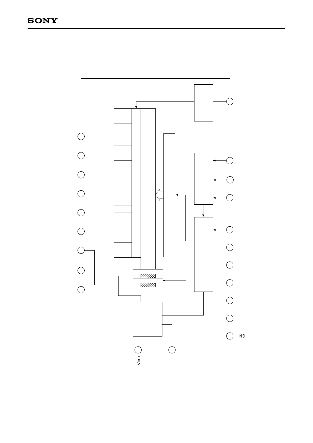
Read out gate
CCD analog shift register
Clock-drivers
Read out gate
pulse generator
Mode
selector
11
4
10
19
5
9
φROG
SHSW
EXRS
RSSW
φCLK
T1
Block Diagram
DD2
NC
V
21
22
Output amplifier
Sample-and-hold
circuit
1
VOUT
– 2 –
18
VGG
8
Clock pulse generator
Sample-and-hold pulse
generator
7
6
3
2
DD2
DD1
V
GND
V
GND
GND
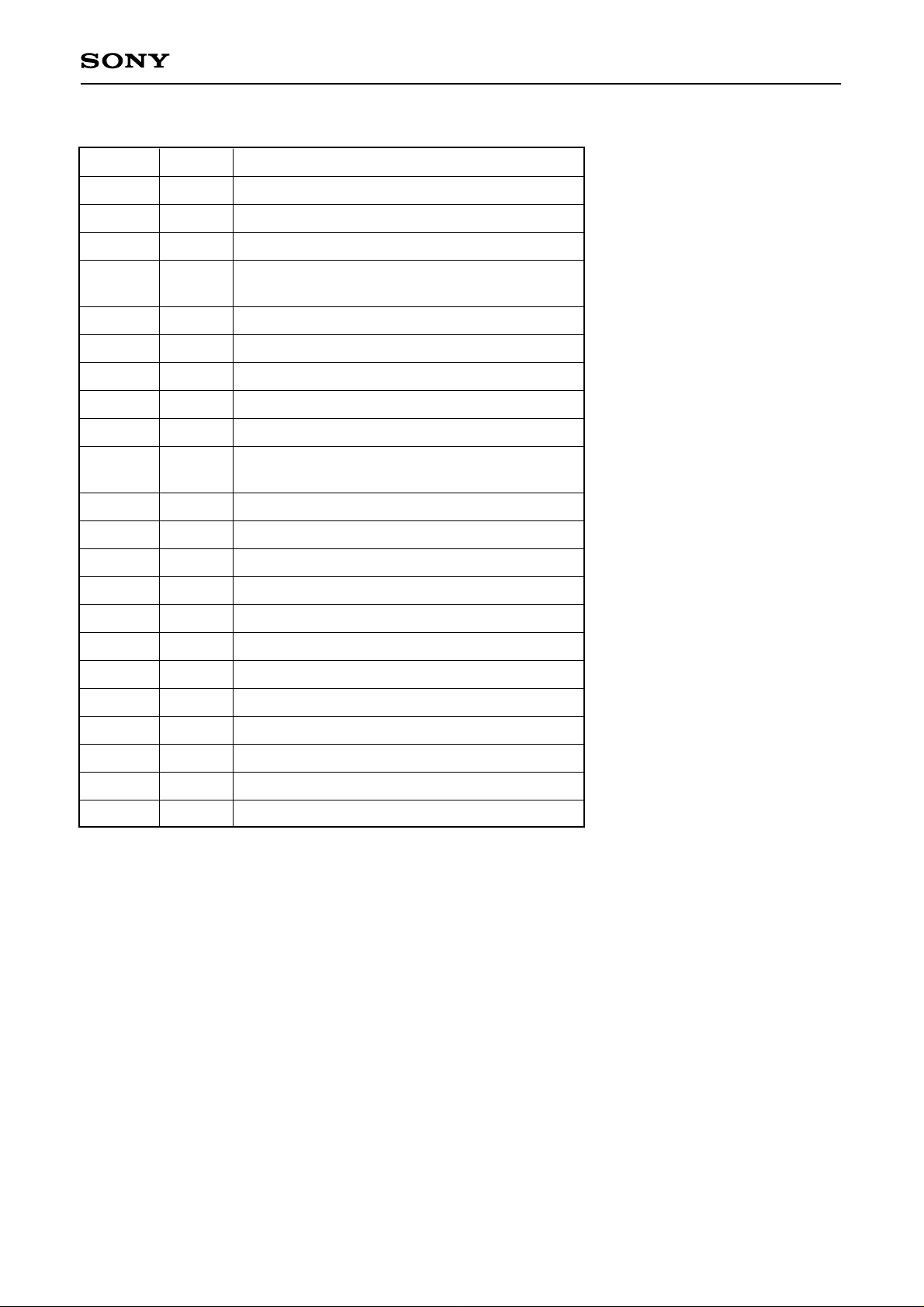
Pin Description
ILX505A
Pin No.
1
2
3
4
5
6
7
8
9
10
11
12
13
14
Symbol
VOUT
GND
GND
SHSW
φCLK
VDD1
GND
VDD2
T1
EXRS
φROG
GND
NC
NC
Description
Signal output
GND
GND
Switch
Clock pulse
9V power supply
GND
5V power supply
Test pin (VDD2)
External RS pulse input. Must be connected to
VDD2 when the internal RS pulse is used.
Clock pulse
GND
NC
NC
with S/H → GND
{
without S/H → VDD2
15
16
17
18
19
20
21
22
VDD1
GND
GND
VGG
RSSW
VDD1
NC
VDD2
9V power supply
GND
GND
Output circuit gate bias
Reset pulse switchover pin
9V power supply
NC
5V power supply
– 3 –
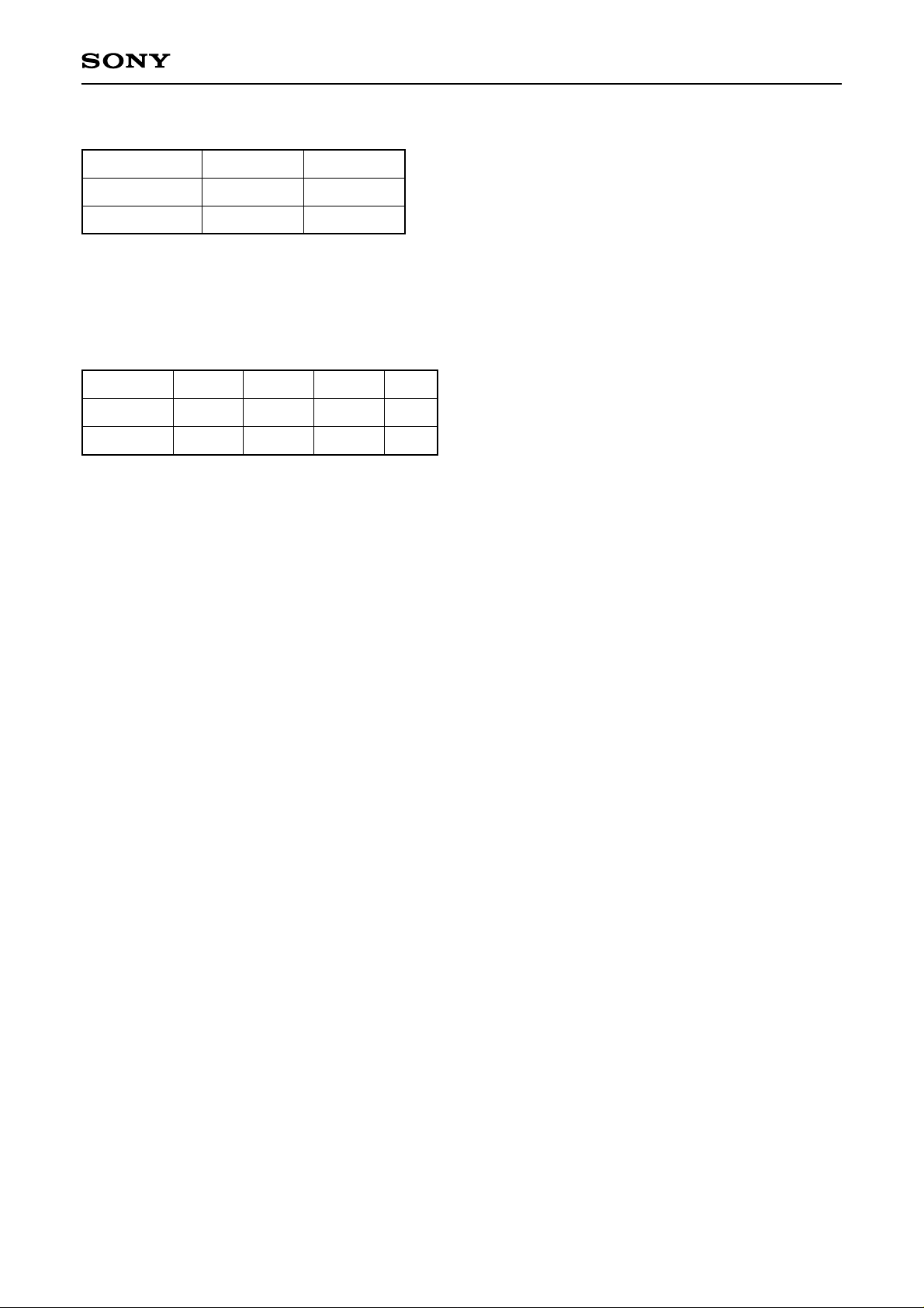
Mode Description
ILX505A
Mode in Use
Internal RS
Externel RS
19 pin RSSW
GND
VDD2
10 pin EXRS
VDD2
φRS
Note) When the external RS mode is in use, operation of use internal S/H is not guaranteed. Pin 4 must be
connected to 5V DC power supply.
Recommended Voltage
Item
VDD1
VDD2
Min.
8.5
4.75
Typ.
9.0
5.0
Max.
9.5
5.25
Unit
V
V
Note) Rules for raising and lowering power supply voltage
To raise power supply voltage, first raise VDD1 (9V) and then VDD2 (5V).
To lower voltage, first lower VDD2 (5V) and then VDD1 (9V).
– 4 –
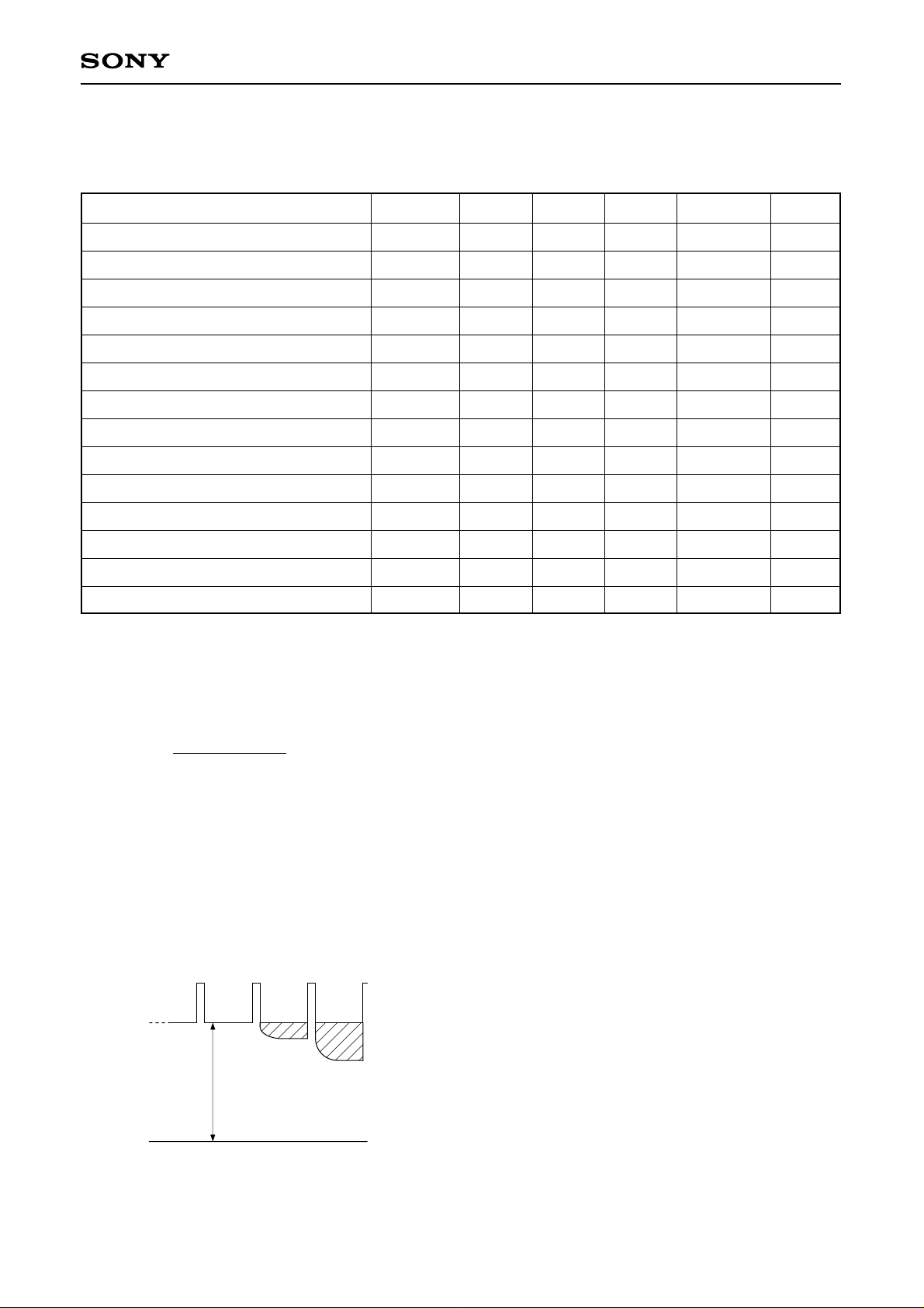
Electro-optical Characteristics
ILX505A
(Ta = 25°C, VDD1 = 9V, VDD2 = 5V, Clock frequency: 1MHz,
Light source = 3200K, IR cut filter: CM-500S (t = 1.0mm)),
When Internal RS (Pin 19 = GND, Pin 10 = VDD2)
Item
Sensitivity 1
Sensitivity 2
Sensitivity nonuniformity
Saturation output voltage
Dark voltage average
Dark signal nonuniformity
Image lag
Dynamic range
Saturation exposure
9V supply current
5V supply current
Total transfer efficiency
Output impedance
Offset level
Symbol
R1
R2
PRNU
VSAT
VDRK
DSNU
IL
DR
SE
IVDD1
IVDD2
TTE
ZO
VOS
Min.
16.8
—
—
1.5
—
—
—
—
—
—
—
92.0
—
—
Typ.
21
53
2.0
1.8
0.3
0.5
0.02
6000
0.085
14.0
5.0
97.0
600
4.5
Max.
25.2
—
8.0
—
2.0
3.0
—
—
—
20.0
10.0
—
—
—
V/(lx · s)
V/(lx · s)
Notes)
1) For the sensitivity test light is applied with a uniform intensity of illumination.
2) W lamp (2854K)
3) PRNU is defined as indicated below. Ray incidence conditions are the same as for Note 1.
Unit
%
V
mV
mV
%
—
lx · s
mA
mA
%
Ω
V
Remarks
Note 1
Note 2
Note 3
—
Note 4
Note 4
Note 5
Note 6
Note 7
—
—
—
—
Note 8
PRNU = × 100 [%]
(VMAX – VMIN)/2
VAVE
The maximum output of all the valid pixels is set to VMAX, the minimum output to VMIN and the average
output to VAVE.
4) Integration time is 10ms.
5) VOUT = 500mV
6) DR = VSAT/VDRK
7) SE = VSAT/R1
8) VOS is defined as indicated below.
Signal is observed at PNP-type emitter follower out.
D32 D33 S1D31
OS
OS
V
GND
– 5 –
 Loading...