

Page 1
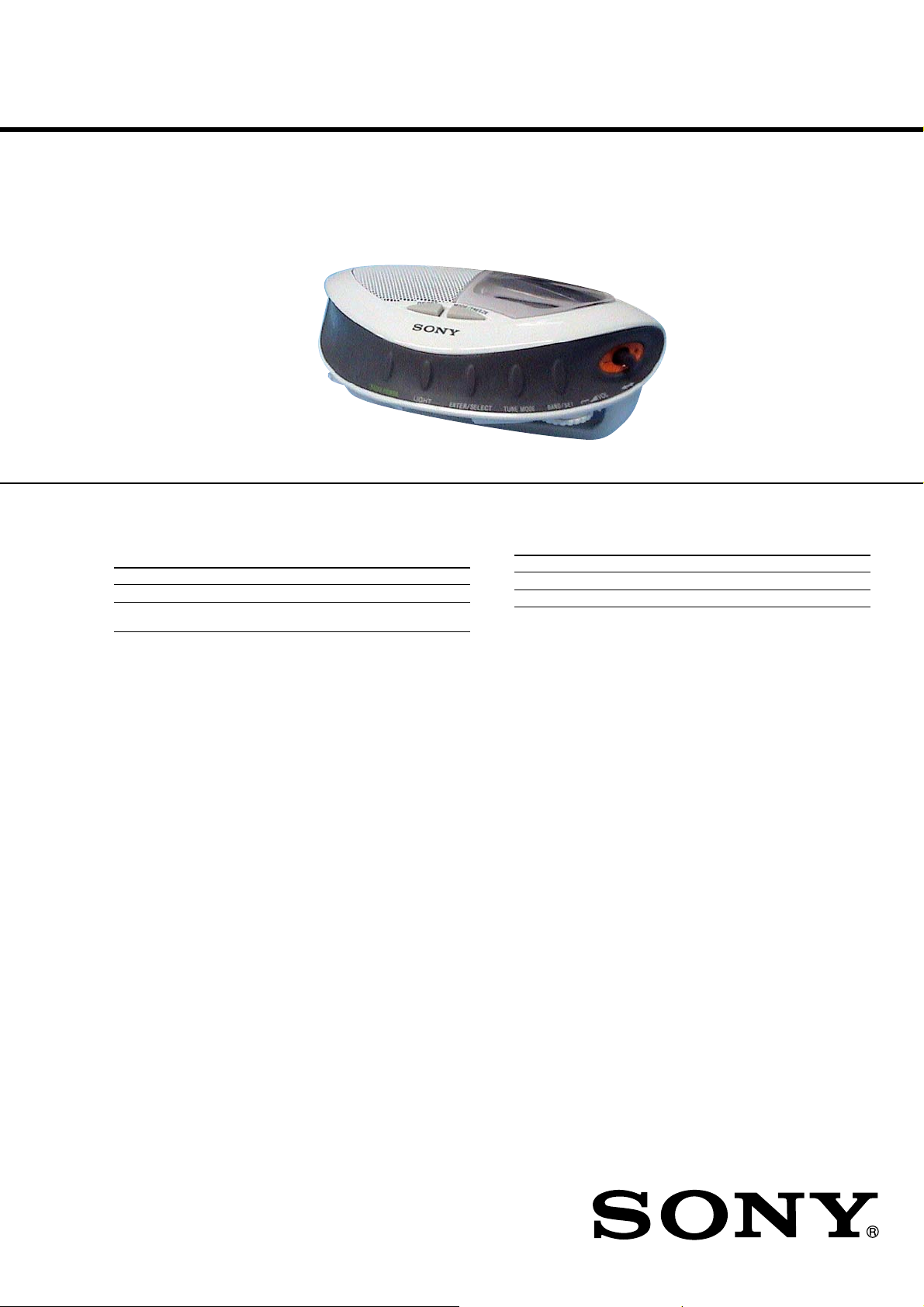
ICF-M88B
SERVICE MANUAL
Ver 1.0 2004.05
SPECIFICATIONS
Time display: 12-hour system
Frequency range:
Band Range Channel step
FM 87.5 - 108 MHz 0.1 MHz
AM 530 - 1 710 kHz 10 kHz
Speaker: Approx. 50 mm (2 inches) dia, 8
Power output: 80 mW (at 10% harmonic distortion)
Power requirements: 3V DC, two size AA (R6) batteries
Dimensions :
Approx. 166.8 × 70 × 95 mm (w/h/d) (6
projecting parts and control.
Mass: Approx. 281.4 g (9.93 oz) incl. batteries / excl. accessories
Supplied accessories:
Mount with wheel sensor (1), Thick/Thin rubber pads (2 each),
Wheel magnet (1), Zip ties (5), Double-sided tape (1), Screws (2)
Design and specifications are subject to change without notice.
531 - 1 710 kHz 9 kHz
5
× 2
⁄
8
7
× 3
⁄
8
3
⁄4 inches) incl.
US Model
Canadian Model
Battery Life (Approx. hours) (JEITA*)
When using FM AM
Sony alkaline size AA (LR6) 66 84
Sony size AA (R6) 23 31
*Measured by JEITA (Japan Electronics and Information Technology Industries
Association) standards.
The actual battery life may vary depending on circumstances of use.
9-877-839-01
2004E05-1
© 2004.05
FM/AM PLL SYNTHESIZED RADIO
Sony Corporation
Personal Audio Company
Published by Sony Engineering Corporation
Page 2

ICF-M88B
SECTION 1
SERVICING NOTES
TABLE OF CONTENTS
1. SERVICING NOTES ............................................... 2
2. GENERAL ................................................................... 3
3. DISASSEMBLY
3-1. Disassembly Flow ........................................................... 4
3-2. Cabinet (Lower) Block.................................................... 4
3-3. Chassis Assy .................................................................... 5
3-4. MAIN Board.................................................................... 5
4. TEST MODE.............................................................. 7
5. ELECTRICAL ADJUSTMENTS ......................... 8
6. DIAGRAMS
6-1. Printed Wiring Boards – TUNER Section –................... 10
6-2. Schematic Diagram – TUNER Section – ....................... 11
6-3. Printed Wiring Board
– PANEL/POWER SUPPLY Section – ........................... 12
6-4. Schematic Diagram
– PANEL/POWER SUPPLY Section – ........................... 13
7. EXPLODED VIEWS
7-1. Cabinet (Upper) Section .................................................. 16
7-2. Chassis Section................................................................ 17
7-3. Cabinet (Lower) Section.................................................. 18
UNLEADED SOLDER
Boards requiring use of unleaded solder are printed with the leadfree mark (LF) indicating the solder contains no lead.
(Caution: Some printed circuit boards may not come printed with
the lead free mark due to their particular size)
: LEAD FREE MARK
Unleaded solder has the following characteristics.
• Unleaded solder melts at a temperature about 40 ˚C higher
than ordinary solder.
Ordinary soldering irons can be used but the iron tip has to be
applied to the solder joint for a slightly longer time.
Soldering irons using a temperature regulator should be set to
about 350 ˚C.
Caution: The printed pattern (copper foil) may peel away if
the heated tip is applied for too long, so be careful!
• Strong viscosity
Unleaded solder is more viscou-s (sticky, less prone to flow)
than ordinary solder so use caution not to let solder bridges
occur such as on IC pins, etc.
• Usable with ordinary solder
It is best to use only unleaded solder but unleaded solder may
also be added to ordinary solder.
8. ELECTRICAL PARTS LIST................................ 19
Notes on chip component replacement
• Never reuse a disconnected chip component.
• Notice that the minus side of a tantalum capacitor may be
damaged by heat.
2
Page 3
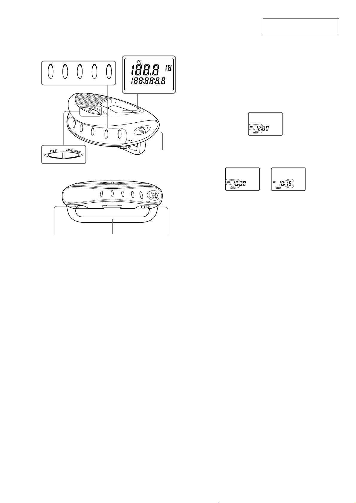
Location of Controls
SECTION 2
GENERAL
ICF-M88B
This section is extracted from
instruction manual.
FREEZE
PRESET
MHz
kHz
MP H
km/h inc h
mile
mm
MP H
km/h
RADIO P OWER LIGHT ENTER /SELE CT TUNE MODE BAND/SE T
RA
DIO
P
O
W
E
R
LIGHT
E
N
T
E
R
/
S
E
L
E
C
T
T
U
N
E
M
O
D
FM
AM
AM
PM
CLOCK ODO DIST RT AVG MAX
OL
V
T
E
S
/
D
E
N
A
B
J og lever
G
H
I
T
L
E
N
R
T
E
W
O
P
O
I
D
A
R
FM an tennaFM SENS
E
R
/
S
E
L
E
C
T
T
U
N
E
M
O
D
E
B
A
N
D
/
S
E
T
V
O
L
VO L*
DX/LOCAL
* Th ere is a tactile dot beside VOL to show the direction to turn up
the volume.
Setting the Clock
The clock time display of this unit is a 12-hour system.
When the batteries are first installed, AM 12:00 flashes and CLOCK turns on
in the display.
1
Press RADIO POWER to turn off the power.
2
Press MODE/FREEZE repeatedly until CLOCK appears.
3
Hold down ENTER/SELECT for more than 2 seconds until
AM 12 starts flashing.
4
Push the Jog lever towards + or – to adjust the hour, then press
ENTER/SELECT.
The beep sounds and the minute setting starts to flash.
If you hold down the Jog lever towards + or —, the digit changes rapidly.
Midnight is indicated as AM 12:00 and Noon is indicated by PM 12:00.
g
5
Repeat step 4 above to adjust the minutes.
: starts flashing and the clock starts operating.
To set the current time exactly to the second, adjust the minute setting and
then press ENTER/S ELE CT to synchronize it with a time signal (such as
the telephone time signal).
Note
If you do not push the Jog lever towards + or —, or ENTE R/S ELECT within
about 65 seconds, the clock setting mode will be canceled.
3
Page 4
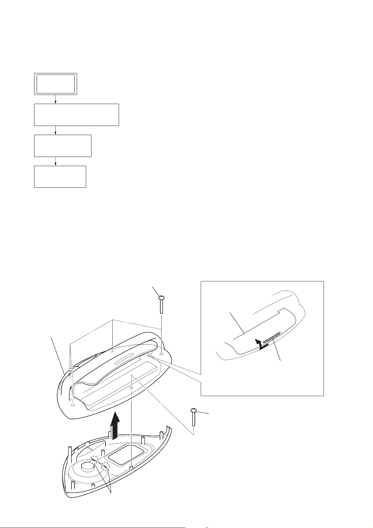
ICF-M88B
• This set can be disassembled in the order shown below.
3-1. DISASSEMBLY FLOW
SET
3-2. CABINET (LOWER) BLOCK
(Page 4)
3-3. CHASSIS ASSY
(Page 5)
3-4. MAIN BOARD
(Page 5)
SECTION 3
DISASSEMBLY
Note: Follow the disassembly procedure in the numerical order given.
3-2. CABINET (LOWER) BLOCK
3
four screws
×
10)
(P1.7
6
cabinet (lower) block
4
battery case lid
2
screw (P1.7 × 10)
1
Slide the hook (battery case lid)
in the direction of arrow,
and open the battery case lid.
5
Remove two solders.
4
Page 5
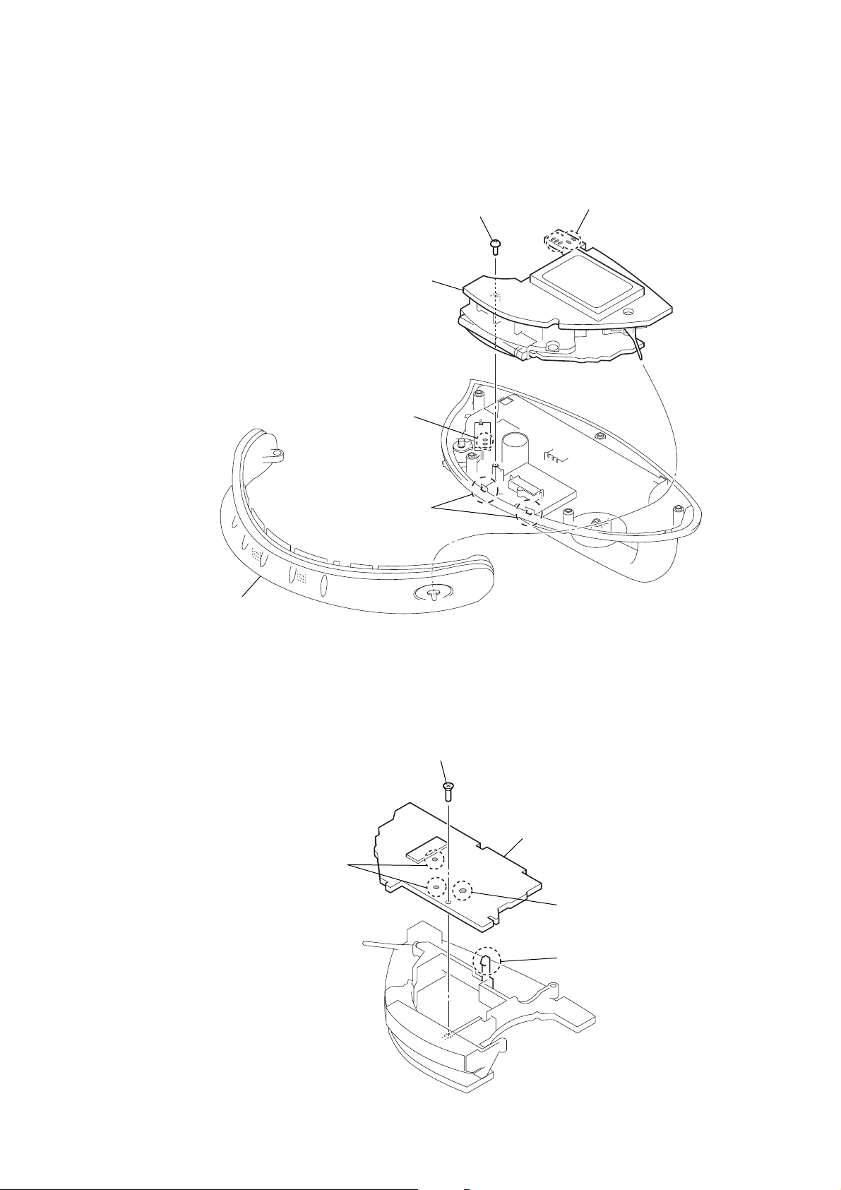
3-3. CHASSIS ASSY
5
chassis assy
1
Remove two solders.
4
screw
1
Remove five solders.
ICF-M88B
3
button assy
3-4. MAIN BOARD
1
Remove two solders.
2
two hooks
3
screw
4
MAIN board
1
Remove the solder.
2
hook
5
Page 6
ICF-M88B
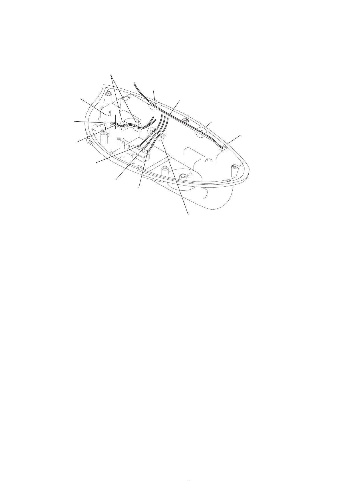
POSITION OF LEAD WIRES
two ditches
boss
DX/LOCAL board
lead wire (gray)
lead wire (red)
lead wire (black)
lead wire (battery terminal (+))
boss
cabinet (lower) block
lead wire (gray)
lead wire (red)
three ditches
6
Page 7

SECTION 4
TEST MODE
ICF-M88B
EEPROM INITIALIZE MODE
Procedure:
1. Turn on the power to place the set in the standby state.
2. Press the [BAND/SET], [LIGHT] and [MODE/FREEZE] keys
simultaneously for 5 seconds, or short the TP116 (KS0) and
TP117 (KR3) on the key board.
3. When the EEPROM initialize mode is activated, the BEEP
1 is outputted and “dEL” is displayed on the LCD for one
second.
4. After one second elapsed, the BEEP 2 is outputted, and the
EEPROM initialize mode is deactivated and the set returns to
the standby state.
LCD AND KEY TEST MODE
Procedure:
1. Turn on the power to place the set in the standby state.
2. Short the TP115 (KS1) and TP117 (KR3) on the key board.
3. When the LCD and key test mode is activated, the BEEP 1 is
outputted and the LCD becomes all lit state.
LCD display
FREEZE
PRESET
FM
AM
AM
PM
CLOCK ODO DIST RT AVG MAX
4. Each time a key is pressed, the segment assigned to each key
turns off (see below). Also, if the [LIGHT] key is pressed, the
LCD back light turns on. (It turns off at the release of LCD
and ket test mode)
5. When all keys were pressed, the BEEP 2 is outputted, and
the LCD and key test mode is deactivated and the set returns
to the standby state.
MHz
kHz
MPH
km/h inch
mile
mm
MPH
km/h
LCD display-3
AM
PM
CLOCK ODO
LCD display-4
DIST
LCD display-5
FM
AM
LCD display-6
FREEZE
LCD display-7
PRESET
MHz
mm
MPH
km/h
Note 1:The pulse input is ignored during each test mode.
Note 2:In the event that the VDET1 terminal (pin rl of IC101) on the k ey
board detects “L” during each test mode, the test mode is deactivated
and the set returns to the standby state.
Note 3:The amplifier power turns on by the main clock operation to prepare
for the BEEP output during each test mode.
Key Segment Display
POWER S0, S2, S4 below LCD display-1
TUNE MODE S6, S8, S10 below LCD display-2
BAND/SET S12, S14, S16 below LCD display-3
+ S18, S20, S22 below LCD display-4
– S3, S5, S7 below LCD display-5
RESET S9, S11, S13 below LCD display-6
MODE/FREEZE S15, S17, S19 below LCD display-7
ENTER/SELECT S21, S23, S25 below LCD display-8
LIGHT S1, S24 below LCD display-9
LCD display-1
kHz
MPH
km/h inch
LCD display-2
LCD display-8
LCD display-9
Connecting Location:
– KEY BOARD (Conductor Side) –
TP117
(KR3)
TP115
(KS1)
IC101
RT AVG MAX
TP116
(KS0)
mile
7
Page 8
ICF-M88B
r
r
r
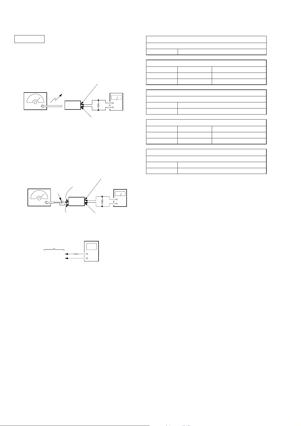
SECTION 5
ELECTRICAL ADJUSTMENTS
0 dB=1 µV
[AM]
Setting:
Function: RADIO
BAND: AM
AM RF signal
generator
30% amplitude
modulation by
400 Hz signal
Output level:
as low as possible
[FM]
Setting:
Function: RADIO
BAND: FM
FM RF signal
generator
22.5 kHz frequency
deviation by 400 Hz
signal
Output level:
as low as possible
Put the lead-wire
antenna close to
the set.
set
MAIN board
TP13 (FM IN)
0.01 µF
set
MAIN board
TP10 (RF GND)
MAIN board
TP12 (SP OUT)
level mete
8
Ω
+
–
MAIN board
TP15 (AF GND)
MAIN board
TP12 (SP OUT)
level mete
8
Ω
MAIN board
TP15 (AF GND)
AM IF ADJUSTMENT
Adjust for a maximum reading on level meter
T1 450 kHz
AM VCO VOLTAGE ADJUSTMENT
Adjustment Part Frequency Display Reading on Digital Voltmeter
L1 530 kHz 1.2 ± 0.1 V
Confirmation 1,710 kHz 7.2 ± 0.5 V
AM TRACKING ADJUSTMENT
Adjust for a maximum reading on level meter
ANT1 590 kHz
CT1 1,490 kHz
FM VCO VOLTAGE ADJUSTMENT
Adjustment Part Frequency Display Reading on Digital Voltmeter
Confirmation 108.0 MHz 8.9 ± 1.0 V
Confirmation 87.5 MHz 2.3 ± 0.5 V
FM TRACKING ADJUSTMENT
Adjust for a maximum reading on level meter
L2 87.5 MHz
CT2 108.0 MHz
Adjustment Location: MAIN board (See page 9)
+
–
digital voltmete
MAIN board
Ω
TP9 (VT)
TP8 (GND)
100 k
• Repeat the procedures in each adjustment several times, and
the tracking adjustments should be finally done by the trimmer
capacitors.
• Remove FM antenna in FM adjustment.
8
Page 9

Adjustment Location:
– MAIN BOARD (Component Side) –
AM IF Adjustment
CT2
FM T rac king Adjustment
L2
ICF-M88B
T1
– MAIN BOARD (Conductor Side) –
(RF GND)
TP10
IC1
AM VCO Voltage Adjustment
CT1
AM T rac king Adjustment
ANT1
TP13
(FM IN)
L1
TP8
(GND)
IC2
TP15
(AF GND)
TP9
(VT)
TP12
(SP OUT)
99
Page 10

ICF-M88B
SECTION 6
DIAGRAMS
• Note for Printed Wiring Boards and Schematic Diagrams
Note on Printed Wiring Boards:
• X : parts extracted from the component side.
• Y : parts extracted from the conductor side.
• W : indicates side identified with part number.
• z : Through hole.
f
•
• : Pattern from the side which enables seeing.
• : Carbon pattern.
(The other layers' patterns are not indicated.)
Caution:
Pattern face side: Parts on the pattern face side seen from
(Conductor Side) the pattern face are indicated.
Parts face side: Parts on the parts face side seen from
(Component Side) the parts face are indicated.
: internal component.
Note on Schematic Diagram:
• All capacitors are in µF unless otherwise noted. (p: pF)
50 WV or less are not indicated except for electrolytics
and tantalums.
• All resistors are in Ω and 1/
specified.
4
W or less unless otherwise
• f : internal component.
• C : panel designation.
• A : B+ Line.
• H : adjustment for repair.
• Power voltage is dc 3 V and fed with regulated dc power
supply from battery terminal.
• Voltages and waveforms are dc with respect to ground
under no-signal (detuned) conditions.
no mark : FM/AM
• Voltages are taken with a V OM (Input impedance 10 MΩ).
Voltage variations may be noted due to normal production tolerances.
• Waveforms are taken with a oscilloscope.
Voltage variations may be noted due to normal production tolerances.
• Circled numbers refer to waveforms.
• Signal path.
F : FM
f : AM
6-1. PRINTED WIRING BOARDS – TUNER Section –
1 2 3 4 5 6
ANT2
A
B
C
D
FM LEAD-WIRE
ANTENNA
MAIN BOARD
DX/LOCAL BOARD
L301
LOCAL DX
+
C17
JC6
A
K
R6
R14
A
D4
C18
+
C21
+
R8
R12
S301
FM SENS
R23
C25
RED
GRAY
R302
11
(11)
1-862-331-
C20
C16
C23
15
28
CF2
TP15
(AF GND)
JW8
TP10 (RF GND)
R10
T1
IC1
JW4
RED
GRAY
TP13
(FM IN)
1
R9
C27
+
14
3
BPF1
C26
L3
C28
C31
1
+
C30
CF3
R11
JW6
JW7
CF1
Q2
ECB
C15
JC5
JC8
Q1
ECB
C29
C19
C13
+
C24
RV1
VOL
R4
C12
R24
:Uses unleaded solder.
A
(Page 12)
BLK
C32
C10
C9
C8
JC4
JC9
C11
JC3
1
5
BCE
Q3
RED
GRY
8
D2
KA
R3
CT2
R25
R5
KA
D3
L1
C6
C14
R13
RED
GRY
C35
JC11
JC10
C40C38
1
L2
IC2
10
C47
C46
R2
3
C3
A
C4
A
4
CT1
KEY BOARD
BLK
GRY
JC12
20
11
C34
+
TP9
(VT)
C2
K
D1
RED
1
X1
C37
TP8
(GND)
R21
R7
C39
R20
L4
R1
R17
C36R19
C42
C43
C44C45
JW1
JW2
JW3
1
2
TP12
(SP OUT)
C22
+
11
E
• Semiconductor
Location
Ref. No. Location
D1 D-5
D2 C-4
D3 D-4
D4 C-1
IC1 C-3
IC2 C-5
Q1 C-2
Q2 B-2
Q3 D-4
BLK
L1
13
54
NATURAL
ANT1
AM FERRITE-ROD
ANTENNA
RED
RED
SP1
1-862-330-
GRAY
(11)
1010
Page 11

ICF-M88B
6-2. SCHEMATIC DIAGRAM – TUNER Section –
ANT1
AM
FERRITE-ROD
ANTENNA
S301
ANT2
FM LOCAL
LEAD-WIRE
ANTENNA
FM SENS
0.1µH
R302
DX
L301
4.7
• See page 14 for Waveform. • See page 14 for IC Block Diagrams.
JC4
0
TP13
(FM IN)
TP10
(RF GND)
CT1
BPF1
13
2
C2 R1
0.01 10k
SVC347
R2
1M
D1
C6 C14
10p 3p
C3
220p
C4
220p
L1
AM
OSC
C26
0.01
L2
FM
CT2
RF
C27
10
6.3V
C28
3p
R3
100k
C8
1000p
D2
HVU202A
C9
1000p
R24 R25
100k 100k
0
JC3
C30 R11
147
C31
2.2
35V
R4 C10
L3
22k 7p
C32
0.022
CF3
TP9
(VT)
C11
R5
1000p
100k
D3
HVU202A
C12
1000p
JC9
0
R13
2SA1576
MUTING
Q3
10k
C34
470
RV1
50k
VOL
4V
75KHz
R12
4.7k
R17 R21
C36
0.01
10k 100k
C37
C39
22p
22p
X1
R7
2.2k
R19
4.7k
C42 C43
0.1 0.22
C45 C46 C47
1 100p 0.01
p
4
0
4
C
20
2
R20
2.2k
MIX
F.E
OUT
FM/AM FRONT-END,
FM/AM IF AMP,DET,
AGC,AF AMP
IC1
CXA1019M
C15
0.01
R10
470
R9
T1
2.2k
AM IFT
CF1 CF2
TP12
(SP OUT)
SP1
GNDFMANT
BAND AM FM IF AFC(W) AFC(J) DET AF RIPPLE AF
JC8
0
NC AM
C16
1
DTC114TUA
FM/AM BAND
SELECT SWITCH
C22
470
4V
ANTFMRF
JC5
0
Q2
C23
1
REG FM
JC6
0
C17 C18
4.7
16V106.3V
R6 R14
10k 10k
D4
DAN202UT
AFC AM
OSC
R23
4.7k
TONE CONTROL
C25
1000
6.3V
C20
0.22
2SC4081
SWITCH
OSC
C21
6.3V
C29
0.01
Q1
VOL NF DISCRI GND
10
0p
0
47
3
1
C
C19
0.01
C24
1
GNDOUT+BFILTERINOUTAGCAGCGNDMETERNCIFINIFINSELECT
TP15
(AF GND)
R8
2.2k
L4
47µH
XXVSSAAAPD VSSD VDD FM AM
CE DI CL DO BAND BO2 BO3 IO1 IO2 IN
FM/AM PLL
IC2
LC72122V
10
C
J
100p4700p 100p
0
C38C35 C40
11
0
C
J
12
0
C
J
INININOUT INOUT
IF
CE
DATA
CLK
DOUT
MUTE
(GND)
BEEP
TP8
(Page 13)
VDD
GND
1111
Page 12

ICF-M88B
6-3. PRINTED WIRING BOARD – PANEL/POWER SUPPLY Section –
1 2 3 4 5 6 7 8 9 10 11 12 13 14 15 16
KEY BOARD
A
(COMPONENT SIDE)
B
BLK
GRY
SENSOR
UNIT
DRY BATTERY
SIZE "AA"
(IEC DESIGNATION R6)
2PCS. 3V
RED
RED
GRY
RED
GRY
BLK
1
A
RED
MAIN
BOARD
(Page 10)
GRY
BLK
RED
GRY
8
C
16
D
30
LCD101
LIQUID CRYSTAL DISPLAY
: Uses unleaded solder.
1
15
S102
C119
E
R144
L104
60
41
R145
R124
R117
C112
C111
Q107
B
C
C114
C115
C116
R122
R121
R120
R119
R118
R115
R114
IC103
C122
C108
43
IC102
R106
R112
R107R116
R108
R105
IC104
KA
D101
C154
14
85
C107
D102
JC102
124312
R101
C105
D109
C152
KA
Q103
BCE
R103
R102
KA
R146
R190
R127
D105
(LCD BACK LIGHT)
(KR3)
L101
R138
C128
X102
R123
Q106
C102
BCE
C104
Q104
C125
C146
R140
C124
C140
R143
R141
C139
C141
R179
R133
R135
R136
C138
C142
Q105
C135
C143
KEY BOARD
T101
+
S101
–
D106
(LCD BACK LIGHT)
Q101
BCE
Q102
C109
(CONDUCTOR SIDE)
R129
AK
D103
C118
R126
R104
R109
D104
+
C117
BCE
AK
C151
R110
R111
R139
C126
IC105
C133
R178
12
43
C129
ECB
ECB
R134
C121
80 61
1
X101
C136
C130
C131
R128
C101
C103
TP117
IC101
R180
+
TP115
(KS1)
20
21 40
R188
R189
R187
E
F
G
RADIO POWER
H
• Semiconductor
Location
Ref. No. Location
D101 B-14
D102 D-14
D103 B-10
D104 C-10
D105 B-15
D106 B-10
D109 B-14
S109
S103
RESET
S108
LIGHT
S106
MODE/FREEZE
S105
ENTER/SELECT
S104
TUNE MODE
S107
BAND/SET
1-862-332-
11
(11)
R183
C155
C158
R182
TP116
(KS0)
R181
C149
C156
R184
C127
+
C157
R185
R186
1-862-332-
11
(11)
IC101 C-12
IC102 C-14
IC103 D-14
IC104 D-14
IC105 C-11
Q101 C-9
Q102 C-9
Q103 B-15
Q104 B-12
Q105 B-12
Q106 A-13
Q107 A-13
1212
Page 13

ICF-M88B
6-4. SCHEMATIC DIAGRAM – PANEL/POWER SUPPLY Section –
R102
470k
R103
470k
R124
100k
D109
RB520
C152
0.01
D102 R101
1SS355 2.2M
VOLTAGE DETECT
S-80821CNNB
R107R112
1k1k
C116
4700p
C108
100p
C151
2.2
35V
Q106,107
POWER ON/OFF
CONTROL SWITCH
IC103
JC102
D103 R104
1SS355 1k
Q107
2SB970
R105 R108
1M 1M
0
T
IN
U
O
D
D
N
N
G
G
C105
0.1
EEPROM
IC102
BR24L01F-WE2
DC/DC
CONVERTER
C109 Q101 Q102
10p 2SC4081 2SC4081
R144
1k
Q106
DTC144TUA
T
IN
U
O
D
D
N
N
G
G
C111
C112
C122
0.01
R116
10k
T101
R145
100k
R146
470k
SENSOR
UNIT
(Page 11)
CE
DATA
CLK
DOUT
MUTE
BEEP
VDD
GND
R187
R189
R188
C114 C115
100p 100p
1k
1k
1k
• See page 14 for Waveforms. • See page 15 for IC Pin Function Description.
Q103
(LCD BACK LIGHT)
VOLTAGE DETECT
IC104
S-80819CNNB
0.01
0.1
C107
0.01
C
K
P
L
C
W
C
V
2
1
0
A
A
A
Q101,102
DC/DC
CONVERTER
2SA1576
LED DRIVE
D105,106
D105
R115 R114
470k 10k
R118
R119
R120
R121
R122
R106
10k
A
T
A
D
D
N
G
UDZSTE-1713B100k 0.1
• TOTAL CURRENT
FM: 18mA
AM: 11mA
(NO-SIGNAL CONDITION)
D106
SLI-343OUT
SLI-343OUT
R129R127 C154 R190
100100 0.1 10k
R117
1k
1k
1k
1k
1k
1k
D104R109 C117
DRY BATTERY
SIZE"AA"
(IEC DESIGNATION R6)
2PCS. 3V
R126
220
R110
100k
R111 C118
47k 1
P65
P64
P63
P62
P61
P60
AVSS
VDET2
VDET1
BEEP
PS
MOUNT
MUTE
P24
DATA/EEPROM
CLK/EEPRON
DATA/PLL
CLK/PLL
CE/PLL
P10
C127
0.047F
5.5V
D
6
D
IO
P
V
S
A
R
E
V
R
E
W
7
D
O
0
E
L
P
P
TP117
(KR3)
R123
1k
L104
100µH
C119
10
6.3V
2
2
8
8
S
S
P
P
0
1
2
3
R
R
R
R
K
K
K
K
100p
C149
2
2
S
S
SYSTEM CONTROLLER
IC101
µPD789488GC-A35
0
0
0
IC
P
R138
220k
6p
C102
X102
22p
C128
L101
22µH
C101 D101
1
RB521S
2
S
-8BT
1
T
X
32.768KHz
2
S
2
T
X
22p
C104
1
1
1
1
S
S
S
S
D
S
2
1
S
D
X
X
V
V
1
1
C103
C121
C130
22p
C129
10p
Q104
2SA1576
SHIFT
CLOCK
R128 R140 R143
1M 10k 10k
S101 S102
R180
2.2k
TUNE MODE ENTER/SELECT
R181
2.2k
R182
2.2k
6
7
8
9
0
1
2
3
4
5
6
7
6
N
LCD101
LIQUID CRYSTAL DISPLAY
1
2
3
4
5
1
S
T
E
S
E
R
1
1
1
1
S
S
S
S
COM3
COM2
COM1
COM0
VLC0
VLC1
VLC2
CAPL
CAPH
T
IF
0
1
2
S
S
S
H
K
K
K
S
X101
4.19MHz
C131
10p
R178 R179
100k 100k
C133 C135
0.01 0.01
+-
1000p1000p
C155C158
S105S104
1000p
C156
LIGHTBAND/SET RADIO POWER
1000p
C157
0
7
8
9
1
S
S
S
S
S10
S9
S8
S7
S6
S5
S4
S3
S2
S1
S0
R141
C136
22p
R183
2.2k
R184
2.2k
R185 R186
2.2k 2.2k
5
6
S
S
10k
Q105
2SA1576
SHIFT
CLOCK
MODE/FREEZE
RESET
4
S
C139
9p
C138
22p
R134
1M
S103
S106
S109S108S107
S
S
S
S
1
C140
1
C141
1
C142
C143
1
RESET SIGNAL
GENERATOR
R139
1M
IN
D
N
G
C
CO
C
C
S10
S9
S8
S7
S6
S5
S4
S3
S2
S1
S0
COM3
COM2
COM1
COM0
2.2k
2.2k
2.2k
C146
0.01
T
U
O
D
IC105
N
G
S-80817CNNB
TP115
(KS1)
TP116
(KS0)
R136
R135
R133
470p
470p
470p
C126
C125
C124
0
1
3
2
M
M
M
O
OM
O
0
1
2
3
1313
Page 14

ICF-M88B
p
• Waveforms
– MAIN Board –
IC2 w; (X OUT)
1
500 mV/DIV, 5 µs/DIV
13.3 µs
1.1 Vp-p
– KEY Board –
IC101 ua (XT2)
qa
1 V/DIV, 10 µs/DIV
IC101 ug (X2)
qs
239 ns
1 V/DIV, 100 ns/DIV
Q101 (Collector)
qd
30.5 µs
2.5 Vp-p
2.2 Vp-
• IC Block Diagrams
– MAIN Board –
IC1 CXA1019M-T6
FM/AM
IF OUT
14 13
15
SELECT
FM/AM BAND
FE GND
16
AM IF IN
FM RF IN
NC
12 10
11
FM IF
18
17
NC
FM IF IN
AM RF IN
TUNING METER
19
METER
FM RF
987 216 5 34
20
IF GND
FM OSC
REG OUT
FM FE
FM
DISCRIMINATOR
AM FE
AM IF DET AGC
21
22
AFC AGC
AFC AGC
AFC
23
DET OUT
AM OSCNFVOL
24
AF IN
AF POWER AMP
26
25
RIPPLE FILTER
VCC
FM DISCRI
27
AF OUT
GND
28
GND
Q101 (Base),
qf
Q102 (Collector)
500 mV/DIV, 100 ns/DIV
263 ns
1 V/DIV, 100 ns/DIV
263 ns
1.9 Vp-p
1.2 Vp-p
IC2 LC72122V-TLM-E
CE
1
DI
2
CCB
3
4
5
6
7
8
9
10
UNIVERSAL
COUNTER
I/F
PROGRAMMABLE
LATCH
DATA SHIFT REGISTER
CL
DO
B01
B02
B03
I01
I02
IFIN
12BITS
DIVIDER
UNLOCK
DETECTOR
SWALLOW
COUNTER
1/16,1/17
4BITS
REFERENCE
DIVIDER
PHASE
DETECTOR
CHARGE
PUMP
POWER ON
RESET
1/2
20
XOUT
XIN
19
VSSA
18
17
AOUT
16
AIN
PD
15
VSS
14
13
VDD
FMIN
12
AMIN
11
1414
Page 15

ICF-M88B
• IC Pin Function Description
KEY BOARD IC101 µPD789488GC-A35-8BT (SYSTEM CONTROLLER)
Pin No. Pin Name I/O Description
1, 2 CAPH, CAPL — Terminal for doubler circuit capacitor connection to develop liquid crystal display drive voltage
3 to 5 VLC2 to VLC0 — Terminal for doubler circuit capacitor connection to develop liquid crystal display drive voltage
6 to 9 COM0 to COM3 O
10 to 35 S0 to S25 O
36, 37 P86, P87 O
38
39
40 to 46 P66 to P60
47 AVSS — Ground terminal (for A/D converter)
48 VDET2 I Voltage detection signal input terminal “L”: 2.1V or less
49 VDET1 I Voltage detection signal input terminal “L”: 1.9V or less
50
51 PS I Pulse signal input terminal for 1 rotation time measurement
52 MOUNT I Mount state detection signal input terminal “L”: mount connected, “H”: no connected
53 MUTE O Radio output muting on/off control signal output terminal “L”: muting on
54
55
56 CLK/EEPROM O Serial clock signal output to the EEPROM
57 DATA/PLL O Serial data output to the FM/AM PLL
58 CLK/PLL O Serial clock signal output to the FM/AM PLL
59 CE/PLL O Chip enable signal output to the FM/AM PLL
60, 61 P10, P07 O
62 POWER O
63
64 KR3 I Key return signal input terminal Not used
65 to 67 KR2 to KR0 I Key return signal input terminal
68 P00 O
69 IC0 — Connected to the ground
70 XT1 I Sub system clock input terminal (32.768 kHz)
71 XT2 O Sub system clock output terminal (32.768 kHz)
72
73 VSS — Ground terminal
74 X1 I Main system clock input terminal (4.19 MHz)
75 X2 O Main system clock output terminal (4.19 MHz)
76 RESET I
77 SHIFT O Shift clock on/off control signal output terminal “L”: shift clock on
78 to 80 KS2 to KS0 O Key source signal output terminal
AVDD — Power supply terminal (+2.41V) (for A/D converter)
VERSION I Setting terminal for the destination Fixed at “H” in this set
BEEP O Beep sound output to the FM/AM front-end
P24 O
DATA/EEPROM I/O
LED O
VDD — Power supply terminal (+2.4V)
Common drive signal output to the liquid crystal display
Segment drive signal output to the liquid crystal display
Not used
I Not used
Not used
Two-way data bus with the EEPROM
Not used
Radio power on/off control signal output terminal “H”: power on
LED drive signal output of the liquid crystal display back light “L”: LED on
Not used
System reset signal input from the reset signal generator “L”: reset
For several hundreds msec. after the power supply rises, “L” is input, then it changes to “H”
15
Page 16

ICF-M88B
SECTION 7
EXPLODED VIEWS
NOTE:
• -XX and -X mean standardized parts, so they
may have some difference from the original
one.
• Color Indication of Appearance Parts
Example:
KNOB, BALANCE (WHITE) . . . (RED)
↑↑
Parts Color Cabinet's Color
7-1. CABINET (UPPER) SECTION
• Items marked “*” are not stocked since they
are seldom required for routine service. Some
delay should be anticipated when ordering
these items.
• The mechanical parts with no reference
number in the exploded views are not supplied.
3
not supplied
SP1
1
cabinet (lower) section
2
4
chassis section
5
5
Ref. No. Part No. Description Remark
1 A-4578-032-A BUTTON ASSY
2 1-786-739-11 SWITCH, RUBBER KEY
3 A-4578-030-A CABINET (UPPER) ASSY
16
Ref. No. Part No. Description Remark
4 3-254-083-01 SCREW
5 2-059-726-01 + TAPPING SCREW P1.7X10
SP1 1-825-832-11 SPEAKER (5.0cm)
Page 17

7-2. CHASSIS SECTION
ICF-M88B
65
57
LCD101
54
ANT1
53
51
KEY board
59
60
55
61
64
63
62
55
58
52
51
Ref. No. Part No. Description Remark
51 3-254-083-01 SCREW
52 A-4547-686-A MAIN BOARD, COMPLETE
53 3-267-227-01 CHASSIS
54 A-4547-690-A KEY BOARD, COMPLETE
55 1-780-143-11 CONDUCTIVE BOARD, CONNECTION
56 3-267-229-01 HOLDER (LCD)
57 3-267-252-01 SHIELD (LCD)
58 2-059-727-01 SHEET, REFLECTOR
59 3-267-254-01 SHIELD (DD), A
Ref. No. Part No. Description Remark
60 2-055-147-01 SHIELD (DD), B
61 3-267-233-01 LEVER, JOG
62 2-176-535-01 SHEET (A), REFLECTION
63 2-177-240-01 SHEET, LIGHT INTERCEPTION
64 2-177-241-01 SHEET (BOTTOM), REFLECTION
65 2-177-764-01 SHEET (B), LIGHT INTERCEPTION
ANT1 1-456-789-11 COIL, FERRITE-ROD ANTENNA (MW)
LCD101 1-805-611-11 DISPLAY PANEL, LIQUID CRYSTAL
17
Page 18

ICF-M88B
7-3. CABINET (LOWER) SECTION
117
not supplied
(DX/LOCAL board)
115
105
111
112
107
118
116
104
109
102
114
108
not supplied
not supplied
104
110
103
113
101
Ref. No. Part No. Description Remark
101 A-4578-031-A CABINET (LOWER) ASSY
102 3-267-238-01 CASE (LOWER), ANTENNA
103 3-267-261-01 SPRING (ANTENNA)
104 2-025-137-01 SCREW (1.4X4)
105 3-267-236-01 KNOB (DX/LOCAL)
107 2-059-726-01 + TAPPING SCREW P1.7X10
108 3-267-231-01 LID (MIDDLE), BATTERY CASE
109 3-267-246-01 HOOK (BATTERY CASE LID)
110 3-267-260-01 SPRING (BATTERY CASE LID)
Ref. No. Part No. Description Remark
111 3-236-793-01 O RING (VOL)
112 3-267-235-01 KNOB (VOL)
113 3-267-237-01 CASE (UPPER), ANTENNA
114 3-265-204-01 WASHER, POLYETHYLENE
115 3-267-234-01 ADAPTOR
116 3-267-262-01 RING (BATTERY CASE LID), O
117 3-254-083-01 SCREW
118 7-626-308-61 SPRING-PIN 1.4X14
18
Page 19

SECTION 8
ELECTRICAL PARTS LIST
ICF-M88B
DX/LOCAL KEY
NOTE:
• Due to standardization, replacements in the
parts list may be different from the parts
specified in the diagrams or the components
used on the set.
• -XX and -X mean standardized parts, so they
may have some difference from the original
one.
• RESISTORS
All resistors are in ohms.
METAL: Metal-film resistor.
METAL OXIDE: Metal oxide-film resistor.
F: nonflammable
Ref. No. Part No. Description Remark Ref. No. Part No. Description Remark
DX/LOCAL BOARD
***************
< COIL >
L301 1-412-967-31 INDUCTOR 0.1uH
< RESISTOR >
R302 1-216-793-11 METAL CHIP 4.7 5% 1/10W
< SWITCH >
• Items marked “*” are not stocked since they
are seldom required for routine service.
Some delay should be anticipated when
ordering these items.
• SEMICONDUCTORS
In each case, u: µ, for example:
uA... : µA... uPA... : µPA...
uPB... : µPB... uPC... : µPC...
uPD... : µPD...
• CAPACITORS
uF: µF
• COILS
uH: µH
C126 1-162-962-11 CERAMIC CHIP 470PF 10% 50V
C127 1-125-701-11 DOUBLE LAYER 0.047F 5.5V
C128 1-162-919-11 CERAMIC CHIP 22PF 5% 50V
C129 1-162-915-11 CERAMIC CHIP 10PF 0.5PF 50V
C130 1-162-919-11 CERAMIC CHIP 22PF 5% 50V
C131 1-162-915-11 CERAMIC CHIP 10PF 0.5PF 50V
C133 1-162-970-11 CERAMIC CHIP 0.01uF 10% 25V
C135 1-162-970-11 CERAMIC CHIP 0.01uF 10% 25V
C136 1-162-919-11 CERAMIC CHIP 22PF 5% 50V
C138 1-162-919-11 CERAMIC CHIP 22PF 5% 50V
When indicating parts by reference
number, please include the board.
S301 1-570-675-11 SWITCH, SLIDE (FM SENS)
*************************************************************
A-4547-690-A KEY BOARD, COMPLETE
********************
1-780-143-11 CONDUCTIVE BOARD, CONNECTION
2-055-147-01 SHIELD (DD), B
2-059-727-01 SHEET, REFLECTOR
3-267-229-01 HOLDER (LCD)
3-267-252-01 SHIELD (LCD)
3-267-254-01 SHIELD (DD), A
< CAPACITOR >
C101 1-115-156-11 CERAMIC CHIP 1uF 10V
C102 1-162-911-11 CERAMIC CHIP 6PF 0.5PF 50V
C103 1-115-156-11 CERAMIC CHIP 1uF 10V
C104 1-162-919-11 CERAMIC CHIP 22PF 5% 50V
C105 1-164-156-11 CERAMIC CHIP 0.1uF 25V
C107 1-162-970-11 CERAMIC CHIP 0.01uF 10% 25V
C108 1-162-927-11 CERAMIC CHIP 100PF 5% 50V
C109 1-162-915-11 CERAMIC CHIP 10PF 0.5PF 50V
C111 1-162-970-11 CERAMIC CHIP 0.01uF 10% 25V
C112 1-164-156-11 CERAMIC CHIP 0.1uF 25V
C114 1-162-927-11 CERAMIC CHIP 100PF 5% 50V
C115 1-162-927-11 CERAMIC CHIP 100PF 5% 50V
C116 1-162-968-11 CERAMIC CHIP 0.0047uF 10% 50V
C117 1-164-156-11 CERAMIC CHIP 0.1uF 25V
C118 1-115-156-11 CERAMIC CHIP 1uF 10V
C119 1-126-157-11 ELECT 10uF 20% 16V
C121 1-115-156-11 CERAMIC CHIP 1uF 10V
C122 1-162-970-11 CERAMIC CHIP 0.01uF 10% 25V
C124 1-162-962-11 CERAMIC CHIP 470PF 10% 50V
C125 1-162-962-11 CERAMIC CHIP 470PF 10% 50V
C139 1-162-914-11 CERAMIC CHIP 9PF 0.5PF 50V
C140 1-115-156-11 CERAMIC CHIP 1uF 10V
C141 1-115-156-11 CERAMIC CHIP 1uF 10V
C142 1-115-156-11 CERAMIC CHIP 1uF 10V
C143 1-115-156-11 CERAMIC CHIP 1uF 10V
C146 1-162-970-11 CERAMIC CHIP 0.01uF 10% 25V
C149 1-162-927-11 CERAMIC CHIP 100PF 5% 50V
C151 1-124-257-00 ELECT 2.2uF 20% 35V
C152 1-162-970-11 CERAMIC CHIP 0.01uF 10% 25V
C154 1-164-156-11 CERAMIC CHIP 0.1uF 25V
C155 1-162-964-11 CERAMIC CHIP 0.001uF 10% 50V
C156 1-162-964-11 CERAMIC CHIP 0.001uF 10% 50V
C157 1-162-964-11 CERAMIC CHIP 0.001uF 10% 50V
C158 1-162-964-11 CERAMIC CHIP 0.001uF 10% 50V
< DIODE >
D101 8-719-071-34 DIODE RB521S-30-TE61
D102 8-719-988-61 DIODE 1SS355TE-17
D103 8-719-988-61 DIODE 1SS355TE-17
D104 8-719-083-63 DIODE UDZSTE-1713B
D105 8-719-083-10 LED SLI-343DUT32 (LCD BACK LIGHT)
D106 8-719-083-10 LED SLI-343DUT32 (LCD BACK LIGHT)
D109 8-719-069-29 DIODE RB520S-30TE61
< IC >
IC101 6-804-545-01 IC uPD789488GC-A35-8BT
IC102 6-703-769-01 IC BR24L01AF-WE2
IC103 6-703-324-01 IC S-80821CNNB-B8GT2G
IC104 6-705-588-01 IC S-80819CNNB-B8ET2G
IC105 6-705-589-01 IC S-80817CNNB-B8CT2G
< SHORT >
JC102 1-216-864-11 SHORT CHIP 0
19
Page 20

ICF-M88B
MAINKEY
Ref. No. Part No. Description Remark
< COIL >
L101 1-412-995-21 INDUCTOR 22uH
L104 1-412-963-11 INDUCTOR 100uH
< LIQUID CRYSTAL DISPLAY >
LCD101 1-805-611-11 DISPLAY PANEL, LIQUID CRYSTAL
< TRANSISTOR >
Q101 8-729-905-35 TRANSISTOR 2SC4081-R
Q102 8-729-905-35 TRANSISTOR 2SC4081-R
Q103 8-729-026-52 TRANSISTOR 2SA1576A-T106-R
Q104 8-729-026-52 TRANSISTOR 2SA1576A-T106-R
Q105 8-729-026-52 TRANSISTOR 2SA1576A-T106-R
Q106 8-729-029-15 TRANSISTOR DTC144TUA-T106
Q107 8-729-046-89 TRANSISTOR 2SB970-S (TX).S0
< RESISTOR >
R101 1-216-861-11 METAL CHIP 2.2M 5% 1/10W
R102 1-216-853-11 METAL CHIP 470K 5% 1/10W
R103 1-216-853-11 METAL CHIP 470K 5% 1/10W
R104 1-216-821-11 METAL CHIP 1K 5% 1/10W
R105 1-216-857-11 METAL CHIP 1M 5% 1/10W
R106 1-216-833-11 METAL CHIP 10K 5% 1/10W
R107 1-216-821-11 METAL CHIP 1K 5% 1/10W
R108 1-216-857-11 METAL CHIP 1M 5% 1/10W
R109 1-216-845-11 METAL CHIP 100K 5% 1/10W
R110 1-216-845-11 METAL CHIP 100K 5% 1/10W
R111 1-216-841-11 METAL CHIP 47K 5% 1/10W
R112 1-216-821-11 METAL CHIP 1K 5% 1/10W
R114 1-216-833-11 METAL CHIP 10K 5% 1/10W
R115 1-216-853-11 METAL CHIP 470K 5% 1/10W
R116 1-216-833-11 METAL CHIP 10K 5% 1/10W
Ref. No. Part No. Description Remark
R178 1-216-845-11 METAL CHIP 100K 5% 1/10W
R179 1-216-845-11 METAL CHIP 100K 5% 1/10W
R180 1-216-825-11 METAL CHIP 2.2K 5% 1/10W
R181 1-216-825-11 METAL CHIP 2.2K 5% 1/10W
R182 1-216-825-11 METAL CHIP 2.2K 5% 1/10W
R183 1-216-825-11 METAL CHIP 2.2K 5% 1/10W
R184 1-216-825-11 METAL CHIP 2.2K 5% 1/10W
R185 1-216-825-11 METAL CHIP 2.2K 5% 1/10W
R186 1-216-825-11 METAL CHIP 2.2K 5% 1/10W
R187 1-216-821-11 METAL CHIP 1K 5% 1/10W
R188 1-216-821-11 METAL CHIP 1K 5% 1/10W
R189 1-216-821-11 METAL CHIP 1K 5% 1/10W
R190 1-216-833-11 METAL CHIP 10K 5% 1/10W
< SWITCH >
S101 1-554-088-00 SWITCH, KEY BOARD (–)
S102 1-554-088-00 SWITCH, KEY BOARD (+)
S104 1-554-088-00 SWITCH, KEY BOARD (TUNE MODE)
S105 1-554-088-00 SWITCH, KEY BOARD (ENTER SELECT)
S107 1-554-088-00 SWITCH, KEY BOARD (BAND/SET)
S108 1-554-088-00 SWITCH, KEY BOARD (LIGHT)
S109 1-554-088-00 SWITCH, KEY BOARD (RADIO POWER)
< TRANSFORMER >
T101 1-439-578-11 TRANSFORMER, DC/DC CONVERTER
< VIBRATOR >
X101 1-813-175-11 VIBRATOR, CERAMIC (4.19MHz)
X102 1-760-252-12 VIBRATOR, CRYSTAL (32.768kHz)
*************************************************************
A-4547-686-A MAIN BOARD, COMPLETE
*********************
R117 1-216-821-11 METAL CHIP 1K 5% 1/10W
R118 1-216-821-11 METAL CHIP 1K 5% 1/10W
R119 1-216-821-11 METAL CHIP 1K 5% 1/10W
R120 1-216-821-11 METAL CHIP 1K 5% 1/10W
R121 1-216-821-11 METAL CHIP 1K 5% 1/10W
R122 1-216-821-11 METAL CHIP 1K 5% 1/10W
R123 1-216-821-11 METAL CHIP 1K 5% 1/10W
R124 1-216-845-11 METAL CHIP 100K 5% 1/10W
R126 1-216-813-11 METAL CHIP 220 5% 1/10W
R127 1-216-809-11 METAL CHIP 100 5% 1/10W
R128 1-216-857-11 METAL CHIP 1M 5% 1/10W
R129 1-216-809-11 METAL CHIP 100 5% 1/10W
R133 1-216-825-11 METAL CHIP 2.2K 5% 1/10W
R134 1-216-857-11 METAL CHIP 1M 5% 1/10W
R135 1-216-825-11 METAL CHIP 2.2K 5% 1/10W
R136 1-216-825-11 METAL CHIP 2.2K 5% 1/10W
R138 1-216-849-11 METAL CHIP 220K 5% 1/10W
R139 1-216-857-11 METAL CHIP 1M 5% 1/10W
R140 1-216-833-11 METAL CHIP 10K 5% 1/10W
R141 1-216-833-11 METAL CHIP 10K 5% 1/10W
R143 1-216-833-11 METAL CHIP 10K 5% 1/10W
R144 1-216-821-11 METAL CHIP 1K 5% 1/10W
R145 1-216-845-11 METAL CHIP 100K 5% 1/10W
R146 1-216-853-11 METAL CHIP 470K 5% 1/10W
< BAND PASS FILTER >
BPF1 1-236-711-21 FILTER, BAND PASS
< CAPACITOR >
C2 1-162-970-11 CERAMIC CHIP 0.01uF 10% 25V
C3 1-164-230-11 CERAMIC CHIP 220PF 5% 50V
C4 1-164-230-11 CERAMIC CHIP 220PF 5% 50V
C6 1-162-915-11 CERAMIC CHIP 10PF 0.5PF 50V
C8 1-162-964-11 CERAMIC CHIP 0.001uF 10% 50V
C9 1-162-964-11 CERAMIC CHIP 0.001uF 10% 50V
C10 1-162-912-11 CERAMIC CHIP 7PF 0.5PF 50V
C11 1-115-416-11 CERAMIC CHIP 0.001uF 5% 25V
C12 1-115-416-11 CERAMIC CHIP 0.001uF 5% 25V
C13 1-162-968-11 CERAMIC CHIP 0.0047uF 10% 50V
C14 1-162-908-11 CERAMIC CHIP 3PF 0.25PF 50V
C15 1-162-970-11 CERAMIC CHIP 0.01uF 10% 25V
C16 1-115-156-11 CERAMIC CHIP 1uF 10V
C17 1-124-259-11 ELECT 4.7uF 20% 50V
C18 1-126-157-11 ELECT 10uF 20% 16V
C19 1-162-970-11 CERAMIC CHIP 0.01uF 10% 25V
C20 1-165-128-11 CERAMIC CHIP 0.22uF 16V
C21 1-126-157-11 ELECT 10uF 20% 16V
C22 1-126-518-11 ELECT 470uF 20% 4V
20
Page 21

ICF-M88B
MAIN
Ref. No. Part No. Description Remark
C23 1-115-156-11 CERAMIC CHIP 1uF 10V
C24 1-115-156-11 CERAMIC CHIP 1uF 10V
C25 1-126-916-11 ELECT 1000uF 20% 6.3V
C26 1-162-970-11 CERAMIC CHIP 0.01uF 10% 25V
C27 1-126-157-11 ELECT 10uF 20% 16V
C28 1-162-908-11 CERAMIC CHIP 3PF 0.25PF 50V
C29 1-162-970-11 CERAMIC CHIP 0.01uF 10% 25V
C30 1-115-156-11 CERAMIC CHIP 1uF 10V
C31 1-124-257-00 ELECT 2.2uF 20% 35V
C32 1-164-227-11 CERAMIC CHIP 0.022uF 10% 25V
C34 1-126-518-11 ELECT 470uF 20% 4V
C35 1-162-968-11 CERAMIC CHIP 0.0047uF 10% 50V
C36 1-162-970-11 CERAMIC CHIP 0.01uF 10% 25V
C37 1-162-919-11 CERAMIC CHIP 22PF 5% 50V
C38 1-162-927-11 CERAMIC CHIP 100PF 5% 50V
C39 1-162-919-11 CERAMIC CHIP 22PF 5% 50V
C40 1-162-927-11 CERAMIC CHIP 100PF 5% 50V
C42 1-107-826-11 CERAMIC CHIP 0.1uF 10% 16V
C43 1-127-715-11 CERAMIC CHIP 0.22uF 10% 16V
C44 1-162-966-11 CERAMIC CHIP 0.0022uF 10% 50V
C45 1-115-156-11 CERAMIC CHIP 1uF 10V
C46 1-162-927-11 CERAMIC CHIP 100PF 5% 50V
C47 1-162-970-11 CERAMIC CHIP 0.01uF 10% 25V
Ref. No. Part No. Description Remark
L3 1-456-788-11 COIL, AIR-CORE
L4 1-412-959-11 INDUCTOR 47uH
< TRANSISTOR >
Q1 8-729-905-35 TRANSISTOR 2SC4081-R
Q2 8-729-028-97 TRANSISTOR DTC114TUA-T106
Q3 8-729-026-52 TRANSISTOR 2SA1576A-T106-R
< RESISTOR >
R1 1-216-833-11 METAL CHIP 10K 5% 1/10W
R2 1-216-857-11 METAL CHIP 1M 5% 1/10W
R3 1-216-845-11 METAL CHIP 100K 5% 1/10W
R4 1-216-837-11 METAL CHIP 22K 5% 1/10W
R5 1-216-845-11 METAL CHIP 100K 5% 1/10W
R6 1-216-833-11 METAL CHIP 10K 5% 1/10W
R7 1-216-825-11 METAL CHIP 2.2K 5% 1/10W
R8 1-216-825-11 METAL CHIP 2.2K 5% 1/10W
R9 1-216-825-11 METAL CHIP 2.2K 5% 1/10W
R10 1-216-817-11 METAL CHIP 470 5% 1/10W
R11 1-216-805-11 METAL CHIP 47 5% 1/10W
R12 1-216-829-11 METAL CHIP 4.7K 5% 1/10W
R13 1-216-833-11 METAL CHIP 10K 5% 1/10W
R14 1-216-833-11 METAL CHIP 10K 5% 1/10W
R17 1-216-833-11 METAL CHIP 10K 5% 1/10W
< FILTER >
CF1 1-781-962-21 FILTER, CERAMIC
CF2 1-795-846-11 FILTER, CERAMIC
CF3 1-781-859-11 DISCRIMINATOR, CERAMIC
< TRIMMER >
CT1 1-141-304-21 CAP, CERAMIC TRIMMER
CT2 1-141-304-21 CAP, CERAMIC TRIMMER
< DIODE >
D1 8-719-072-59 DIODE SVC347S-TL-E
D2 8-719-084-67 DIODE HVU202ATRU
D3 8-719-084-67 DIODE HVU202ATRU
D4 8-719-941-86 DIODE DAN202U
< IC >
IC1 8-752-050-16 IC CXA1019M
IC2 6-701-908-01 IC LC72122V-TLM-E
< SHORT >
JC3 1-216-864-11 SHORT CHIP 0
JC4 1-216-864-11 SHORT CHIP 0
JC5 1-216-864-11 SHORT CHIP 0
JC6 1-216-864-11 SHORT CHIP 0
JC8 1-216-864-11 SHORT CHIP 0
R19 1-216-829-11 METAL CHIP 4.7K 5% 1/10W
R20 1-216-825-11 METAL CHIP 2.2K 5% 1/10W
R21 1-216-845-11 METAL CHIP 100K 5% 1/10W
R23 1-216-829-11 METAL CHIP 4.7K 5% 1/10W
R24 1-216-845-11 METAL CHIP 100K 5% 1/10W
R25 1-216-845-11 METAL CHIP 100K 5% 1/10W
< VARIABLE RESISTOR >
RV1 1-227-665-11 RES, VAR, CARBON 50K (w VOL)
< TRANSFORMER >
T1 1-443-316-11 TRANSFORMER, IF
< VIBRATOR >
X1 1-767-388-11 VIBRATOR, CRYSTAL (75kHz)
*************************************************************
MISCELLANEOUS
**************
2 1-786-739-11 SWITCH, RUBBER KEY
ANT1 1-456-789-11 COIL, FERRITE-ROD ANTENNA (MW)
SP1 1-825-832-11 SPEAKER (5.0cm)
*************************************************************
JC9 1-216-864-11 SHORT CHIP 0
JC10 1-216-864-11 SHORT CHIP 0
JC11 1-216-864-11 SHORT CHIP 0
JC12 1-216-864-11 SHORT CHIP 0
< COIL >
L1 1-456-791-11 COIL, OSCILLATION
L2 1-456-851-11 COIL, AIR-CORE
21
Page 22

ICF-M88B
Ref. No. Part No. Description Remark
ACCESSORIES
***********
2-025-136-01 + TAPPING SCREW P2.6X8
(for WHEEL MAGNET)
3-267-406-11 MANUAL, INSTRUCTION (ENGLISH) (US)
3-267-406-21 MANUAL, INSTRUCTION (ENGLISH, FRENCH)
(Canadian)
A-4578-036-A MAGNET ASSY (WHEEL MAGNET)
501 A-4578-034-A BRACKET ASSY
502 2-025-134-01 SCREW M3X10
503 3-267-243-01 JOINT (L), HANDLE
504 3-267-242-01 JOINT (R), HANDLE
505 2-025-138-01 NUT (M3), HEXAGON
506 2-025-133-01 SCREW M3X25
507 3-267-264-01 SHEET (2.5T), RUBBER (THICK RUBBER PAD)
507 3-267-265-01 SHEET (1T), RUBBER (THIN RUBBER PAD)
508 3-267-266-01 SHEET (SENSOR), ADHESIVE
509 3-267-490-01 CLAMP (ZIP TIE)
510 2-025-139-01 SHEET (2T), RUBBER
501
509
Ref. No. Part No. Description Remark
507
506
510
502
not supplied
508
503
505
504
505
510
505
506
507
22
Page 23

MEMO
ICF-M88B
23
Page 24

ICF-M88B
REVISION HISTORY
Clicking the version allows you to jump to the revised page.
Also, clicking the version at the upper right on the revised page allows you to jump to the next revised
page.
Ver. Date Description of Revision
1.0 2004.05 New
2
 Loading...