

Page 1
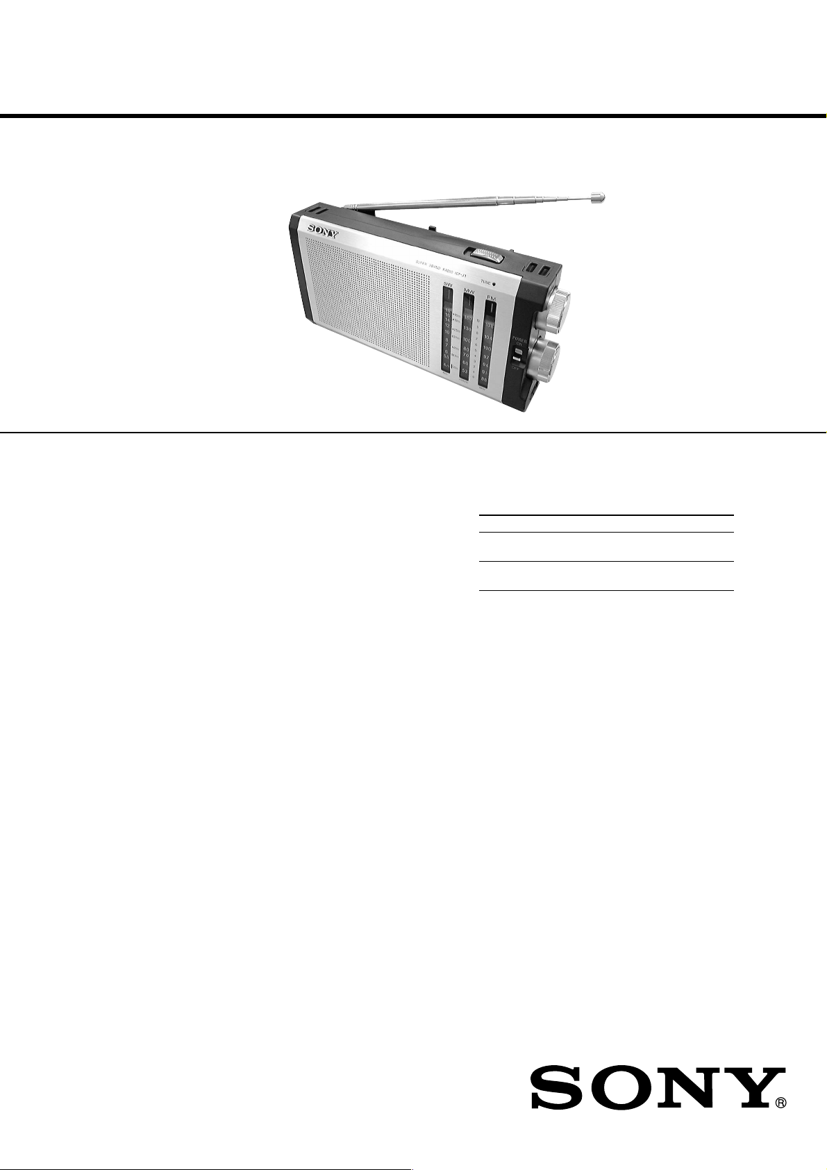
ICF-J1
SERVICE MANUAL
Ver 1.0 2000. 12
SPECIFICATIONS
Frequency range:
FM: 87.5 – 108 MHz
SW: 4.75 – 18.0 MHz
MW: 530 – 1 605 kHz
Speaker
Approx. 9.2 cm (3
Output
v jack (ø 3.5 mm minijack)
Power output
350 mW (at 10 % harmonic distortion)
Power requirements
3 V DC, two R20 (size D) batteries
Dimensions
Approx. 233 × 119.2 × 56 mm (w/h/d)
1
3
/
× 4
(9
and controls
Mass
Approx. 815 g (29 oz) incl. batteries
/
4
5
/
inches) dia., 8 Ω
8
1
× 2
/4 in.) incl. projecting parts
4
E Model
Battery life (approx. hours)
When using FM SW/MW
Sony alkaline 240 250
LR20 (size D) batteries
Sony 120 130
R20 (size D) batteries
Features
• High power sound
• Long battery life with two R20 (size D)
batteries
• High sensitivity
• Easy tuning with the tuning indicator
Supplied accessories
(Middle Eastern model only)
Case (1)
Hand strap (1)
Design and specifications are subject to change
without notice.
FM/SW/MW 3 BAND RADIO
Page 2
SECTION 1
3
GENERAL
TABLE OF CONTENTS
1. GENERAL ................................................................... 2
2. DISASSEMBLY ......................................................... 3
3. ASSEMBLY................................................................. 7
4. ELECTRICAL ADJUSTMENTS......................... 9
5. DIAGRAMS
5-1. Block Diagram ................................................................ 11
5-2. Printed Wiring Board ...................................................... 13
5-3. Schematic Diagram ......................................................... 15
6. EXPLODED VIEWS ................................................ 17
7. ELECTRICAL PARTS LIST ............................... 19
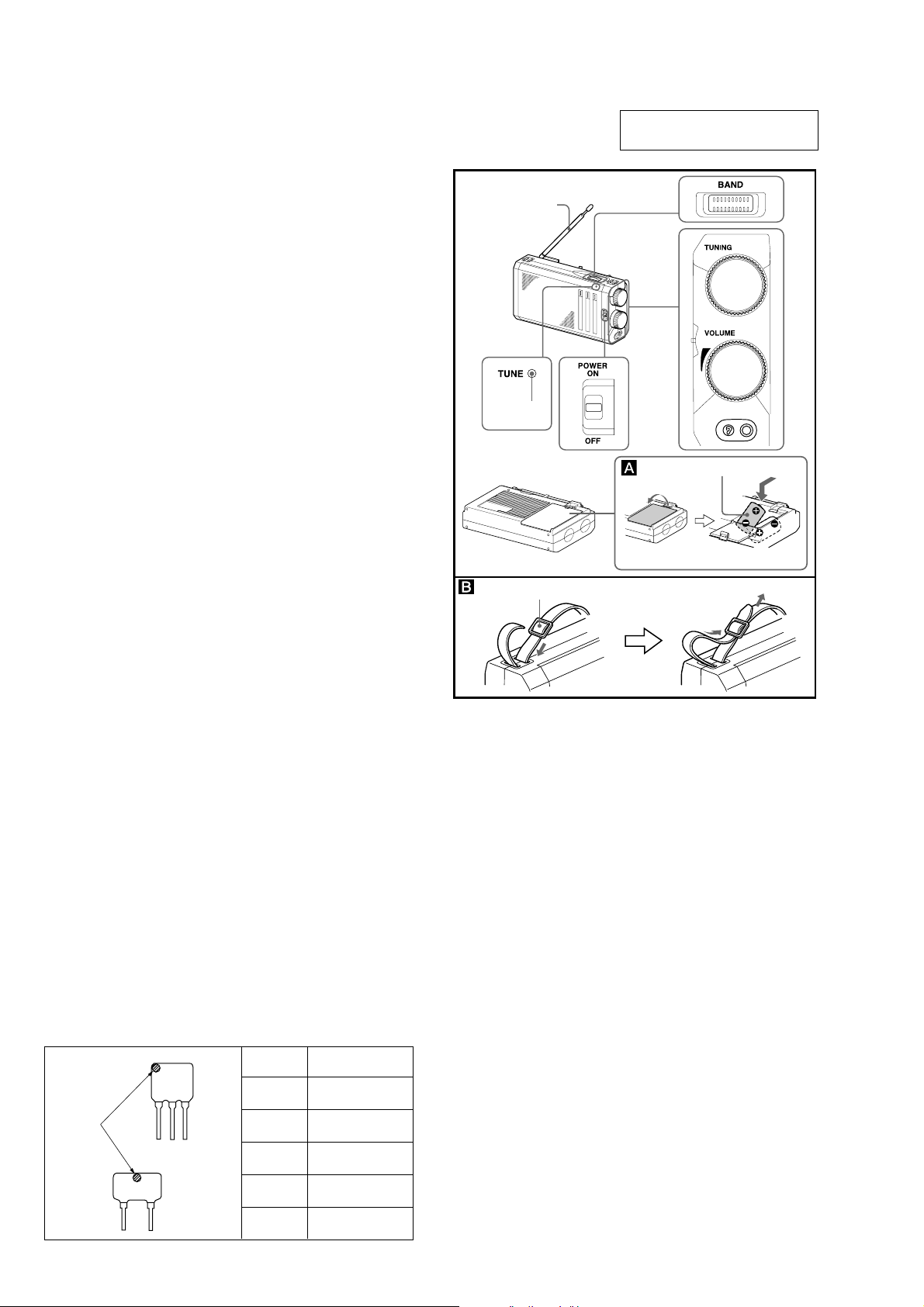
Telescopic antenna
Antena telescópica
indicator
indicador
Pass the strap through the buckle.
Pase la correa a través de la hebilla.
This section is extracted from
instruction manual.
Insert the # side of the battery first.
Inserte en primer lugar la parte # de la pila.
R 20 (size D) × 2
pila R20 (tamaño D) × 2
Notes on chip component replacement
• Never reuse a disconnected chip component.
• Notice that the minus side of a tantalum capacitor may be damaged by heat.
HOW TO CHANGE THE CERAMIC FILTERS
This model is used two ceramic filters of CF1 and CF3.
You must used same type of color marked ceramic filters in order
to meet same specifications.
Therefore, the ceramic filter must changed two pieces together
since it's supply two pieces in one package as a spare parts.
Mark Center frequency
CF
mark
CF1
red 10.70 MHz
blue 10.67 MHz
orange 10.73 MHz
black 10.64 MHz
white 10.76 MHz
– 2 –
Page 3
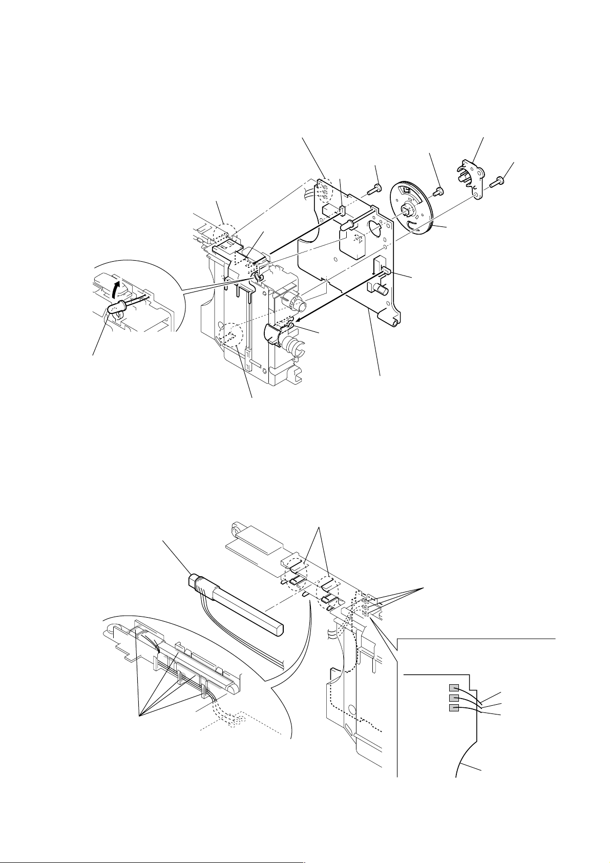
• This set can be disassemble in the order shown below.
e
)
SECTION 2
DISASSEMBLY
Set
Note: Follow the disassembly procedure in the numerical order given.
Lid, Battery Case
“Knob (Tuning)”, “Knob (Volume)”
Chassis Section Main Board Chassis
Antenna, Ferrite-Red (MW) (L1)
Speaker (9.2 cm) (SP1)
LID, BATTERY CASE
“Antenna, Telescopic (FM/SW) (ANT1)”, “Cabinet (Rear)”
“KNOB (TUNING)”, “KNOB (VOLUME)”
Note: Insert the knob (volume) into
the variable resistor (RV1),
meeting both shapes of the hole
in the knob and the shaft of RV1 as shown.
variable resistor (RV1)
2
boss
knob (volume)
1
Open the battery case lid.
2
boss
3
lid, battery cas
2
tuning, spring
3
knob (tuning
hole
– 3 –
5
O ring, P-9
1
4
6
knob (volume)
Page 4
“ANTENNA, TELESCOPIC (FM/SW) (ANT1)”, “CABINET (REAR)”
6
antenna, telescopic
(FM/SW) (ANT1)
2
claw
3
2
claw
4
screw
(P2.6
5
lug, 3
×
8)
Note: Arrange the antenna,
wire to the 4 slots.
antenna, wire
1
7
cabinet (rear)
five screws
(BTP3
×
12)
CHASSIS SECTION
Note: When mounting the battery terminals (+) and (–), engage the lead wires
to the hook on the cabinet (front) and route them as shown.
terminal (–),
battery
hook
cabinet (front)
2
terminal (+),
battery
terminal (+),
battery
3
terminal (–),
battery
1
Remove two solders
of speaker lead wires.
•
LEAD WIRE COLOR INDICATION
ON MAIN BOARD.
MAIN Board
speaker lead wire (RED)
speaker lead wire
(WHT)
SP
3
SP
#
GND
+ B
– 4 –
4
chassis section
battery terminal (–)
lead wire (WHT)
battery terminal (+)
lead wire (WHT/RED)
Page 5
Note: For the mounting position
of the antenna, ferrite-rod (MW) (L1),
refer to the “ANTENNA,
FERRITE-ROD (MW) (L1)”
in DISASSEMBLY.
7
claw
slider
7
claw
8
MAIN board
Note: On installation MAIN board
adjust the S1, S2 and
slider, knob (POWER).
5
gear (tuning capacitor)
Including “spring (gear)”,
“gear (B), tuning capacitor”.
Note: When the gear (tuning
capacity), spring (gear),
and the turning capacitor
gear(B) were removed
and then, they are mounted
on the main board,
refer to the “GEAR
(TUNING CAPACITOR)”,
“SPRING (GEAR)”, “GEAR
(B), TUNING CAPA CIT OR” in
ASSEMBLY on page 8.
6
Remove LED LN21RPL (TUNE)
(D2) by raising in the arrow direction,
not giving an excessive force.
knob
(POWER)
S2
S1
2
screw
(BTP3
×
12)
2
screw
(BTP3
×
12)
1
Remove three solders
of ferrite-rod (MW)
antenna (L1) leads.
4
screw
(B2.6
×
5)
3
holder (gear)
()
MAIN BOARD
2
Remove five portions bond
SC-12N.
Note: When mounting the antenna,
ferrite-rod (MW) (L1), route the lead wires
as shown and apply the bond SC-12N
to the removed portion.
4
antenna, ferrite-rod
(MW) (L1)
3
four claws
1
Remove three solders of
ferrite-rod (MW) antenna (L1)
lead wires.
•
FERRITE-ROD ANTENNA LEAD WIRE
COLOR INDICATION ON MAIN BOARD.
black lead wire
natural lead wire
red lead wire
MAIN board
BLK
NATURAL
RED
ANTENNA, FERRITE-ROD (MW) (L1)
– 5 –
Page 6
SPEAKER (9.2 cm) (SP1)
y
3
Remove speaker (SP1) in the
direction of arrow
2
claw
A
A
.
speaker lead wire (RED)
3
speaker lead wire
(WHT)
#
cabinet (front)
1
speaker (9.2 cm)
(SP1)
claw
Remove shaded portion bond SC-108.
Note: When installing the speaker (SP1),
set it in the position as shown, and apply
the bond SC-108 to the removed portion.
CHASSIS
Note: When assembling the chassis,
refer to the “DIAL POINTER SETTING”
in ASSEMBLY.
qa
plate, back
qd
chassis
qs
3
slider
rack
2
two claws
1
knob (band)
2
two claws
7
two claws
8
6
shaft, tuning
gear, midwa
0
pointer
9
two claws
– 6 –
5
knob (power)
4
4
Page 7

SECTION 3
)
Note: Follow the assembly procedure in the numerical order given.
DIAL POINTER SETTING
•RACK
boss
1
rack
ASSEMBLY
6
5
shaft, tuning
gear, midway
4
pointer
• MAIN BOARD
3
Mount the back plate,
meeting with two bosses of
the chassis.
boss
chassis
a
b
mark
chassis
rack
2
Meet the portion of
the rack with the mark
of the chassis.
a
b
2
claw
– 7 –
2
claw
3
LED LN21RPL (TUNE) (D2)
4
screw
(BTP3
1
MAIN board
×
12
Page 8

• “GEAR (TUNING CAPACITOR)”, “SPRING (GEAR)” AND “GEAR (B), TUNING CAPACITOR”
1
Turn variable condenser (CV1)
gear, midway
shaft fully to the arrow direction
(ant1-clok wise).
2
gear (tuning capacitor)
Including “spring (gear)”,
()
“gear (B), tuning capacitor”.
Note: Adjust so that the triangle
marked is at the position
shown and install.
triangle mark
4
holder (gear)
3
screw (B2.6 × 5)
Note: Secure screw.
Note: Make sure that two tuning capacitor gears
are meshing with the midway gear.
gear, midway
triangle mark
5
screw (BTP3 × 12)
“GEAR (TUNING CAPACITOR)”, “SPRING (GEAR)” AND “GEAR (B), TUNING CAPACITOR” SETTING
gear (tuning capacitor)
1
Insert the spring (gear)
into a hole in the gear
(tuning capacitor).
hook
3
Engage the spring (gear)
to the hook of the tuning
capacitor gear (B) as shown.
spring (gear)
A
– 8 –
2
Fit the tuning capacitor gear (B)
to the gear (tuning capacitor),
and then turn the tuning capacitor gear (B)
in the A direction.
Page 9

SECTION 4
r
r
ELECTRICAL ADJUSTMENTS
0 dB=1 µV
[MW]
Setting:
Band switch: MW
AM RF signal
generator
30% amplitude
modulation by
400 Hz signal
Output level: as low as possible
[SW]
Setting:
Band switch: SW
AM RF signal
generator
30% amplitude
modulation by
400 Hz signal
Output level: as low as possible
[FM]
Setting:
Band switch: FM
FM RF signal
generator
22.5 kHz frequency
deviation by 400 Hz
signal
Output level: as low as possible
Put the lead-wire
antenna close to
the set.
12 pF
0.01 µF
(ANT IN)
(ANT IN)
set
TP1
set
TP1
set
TP8 (SP +)
8
Ω
TP9 (SP –)
TP8 (SP +)
8
Ω
TP9 (SP –)
TP8 (SP +)
8
Ω
TP9 (SP –)
level mete
+
–
level mete
+
–
level meter
+
–
AM IF ADJUSTMENT
Adjust for a maximum reading on level meter
T1 455 kHz
MW FREQUENCY COVERAGE ADJUSTMENT
Adjust for a maximum reading on level meter
L5 516.5 kHz
CT1-4 1,631.5 kHz
MW TRACKING ADJUSTMENT
Adjust for a maximum reading on level meter
L1 600 kHz
CT1-1 1,400 kHz
SW FREQUENCY COVERAGE ADJUSTMENT
Adjust for a maximum reading on level meter
L6 4.7 MHz
CT6 18.5 MHz
SW TRACKING ADJUSTMENT
Adjust for a maximum reading on level meter
L2 4.75 MHz
CT5 18 MHz
FM FREQUENCY COVERAGE ADJUSTMENT
Adjust for a maximum reading on level meter
L4 87.35 MHz
CT1-3 108.25 MHz
FM TRACKING ADJUSTMENT
Adjust for a maximum reading on level meter
L3 87.5 MHz
CT1-2 108 MHz
Adjustment Location: MAIN board (See page 10)
• Repeat the procedures in each adjustment several times, and the
frequency coverage and tracking adjustments should be finally
done by the trimmer capacitors.
• Remove FM/SW antenna in SW and FM adjustments.
– 9 –
Page 10

Adjustment Location:
SW Frequency Coverage
Adjustment
CT6 L6
– MAIN BOARD (Component Side) –
L1 CT1-1
MW Tracking
Adjustment
SW Tracking
Adjustment
L2 CT5
L3 CT1-2
FM Tracking Adjustment
T1
AM IF Adjustment
– MAIN BOARD (Conductor Side) –
MW Frequency
Coverage
Adjustment
CT1-4 L5
CT1-3 L4
FM Frequency Coverage
Adjustment
TP8 (SP +)
TP1 (ANT IN)
TP2 (GND)
TP9 (SP –)
– 10 –
Page 11

5-1. BLOCK DIAGRAM
ICF-J1
SECTION 5
DIAGRAMS
ANT1
FM/SW
TELESCOPIC
ANTENNA
S1 – 1
TRACKING
L1
MW
FERRITE-ROD
ANTENNA
CT1 – 1, L1
TRACKING
CT5, L2
SW
MW
L2
SW ANT
CT1 – 1
L3
FM RF
CT1 – 2, L3 CT1 – 3, L4
FM TRACKING
BPF1
BPF
CT5
S1 – 4
S1 – 3
CV1 – 1
S1 – 5 S1 – 6
CV1 – 4
CV1 – 2 CT1 – 3
CT1 – 4
CT1 – 2 CV1 – 3
10 8
FM RF
FM OSC
FM ANT
13 15 18 24
AM ANT
11
CT1 – 4, L5
MW FREQUENCY
COVERAGE
L5
MW OSC
CT6
FM
FRONT-END
AM
FRONT-END
AM
OSC
6
SW OSC
SW FREQUENCY
COVERAGE
BAND
L6
CT6, L6
MIX OUT
+ +
S1
FM
MW
SW
L4
FM OSC
FM FREQUENCY
COVERAGE
T1
AM IF
AM IF
FM/AM FRONT-END,
FM/AM IF AMP, DET, AGC
IC1
CF3
CF2
FM
IFIN
AM
IFIN
17
CF1
3
DISCRI
FM
DISCRIMINATOR
FM IF
AMP
AM IF,
DET, AGC
TUNING METER
LED
20
D2
TUNE
DET
OUT
BAND
SW
IC2
POWER AMP,
RV1
VOLUME
IN1
13 11
FOR
MW/SW
HIGH CUT
SWITCH
Q1
16
S1 – 2
INVERTER
AMP
RIPPLE FILTER
INV
OUT
REF IN
IN2
RIPPLE FILTER
POWER
AMP
POWER
AMP
Q2
1517
BASE OUT
RIPPLE
FILTER
BATT B+
PWR
OUT1
PWR
OUT2
J1
v
SP1
863
S2
POWER
ON
OFF
(SPEAKER)
DRY BATTERY
SIZE “D”
(IEC DESIGNATION R20)
2PCS. 3V
• SIGNAL PATH
: FM
: MW/SW
05
– 11 – – 12 –
Page 12

ICF-J1
5-2. PRINTED WIRING BOARD
• Semiconductor
Location
Ref. No. Location
D2 A-3
IC1 F-4
IC2 F-7
Q1 G-4
Q2 E-7
A
B
C
D
E
F
G
123 4 5 6 7 8 9
D2
MAIN BOARD
TUNE
+
Q2
BCE
+
R9
IC2
BLK
NATURAL
RED
C22
R8
C27
C39
C33
Note on Printed Wiring Board:
• X : parts extracted from the component side.
• Y : parts extracted from the conductor side.
• W : indicates side identified with part number.
•
• : Pattern from the side which enables seeing.
C30
JW3
10
+
C37
C36
91
C35
R10
JW4
JW5
+
C34
J1
v
VOLUME
TP8 (SP+)
R6
S2
POWER
OFF
ON
RV1
R5
JC8
JW13
R11
L5
MW OSC
CF1
JW12
L6
SW OSC
CT6
C7
JC2
– 6
– 5
C2
C5
C6
L4
FM OSC
115
C41
C4
C45
C10
CV1-1CV1-4
CT1-1CT1-4
CV1-2CV1-3
C3
CT1-2CT1-3
C9
+
R16
CT5
R1
C11
JW2
– 4
– 3
L3
FM RF
3
T1
AM IF
L2
SW ANT
– 2
– 1
1
IC1
C12
R2
CF3
1630
CF2
JW9
JW15
C44
R7
JW10
JW11
C18
C19
C16
+
C17
C20
+
+
+
C13C14C15
Q1
BCE
R4
C21
R3
JC4
JC5
JW8
TP1 (ANT IN)
C1
TP2 (GND)
BPF1
C23
+
JW7
S1
BAND
FM MW SW
JW1
C25
C24
C26
+
C29
C28
18
C31
JC6
C32
JC7
ANT1
FM/SW
TELESCOPIC
ANTENNA
f
: internal component.
C40
JW6
L7
MW FERRITE-ROD ANTENNA
RED
WHT
TP9 (SP – )
WHT
WHT/RED
L1
10
SP1
DRY BATTERY
SIZE “D”
(IEC DESIGNATION R20)
2PCS. 3V
H
+
C38
11
05
– 13 –
– 14 –
1-680-291-
(11)
Page 13

5-3. SCHEMATIC DIAGRAM
• IC Block Diagrams
IC1 CXA1019S
GND
GND
AF OUT
VCC
RIPPLE
FILTER
AF IN
DET OUT
AFC AGC
23 22 21 202425 19 18 17 1629 28 27 2630
AFC AGC
IF GND
METER
ICF-J1
N.C
FM IF IN
AM IF IN
FM/AM BAND
SELECT
AM IF DET AGC
AF POWER AMP AM FE FM IF
FM
DISCRIMINATOR
FM FE
2 345 6 7 8 9
1
GND
GND
NF
FM DISCRI
VOL
AM OSC
AFC
FM OSC
10
REG OUT
TUNING
METER
FM RF
11
IC2 BA6640F-E2
BIAS
RF OUT
RFC
BASE OUT
MUTE OUT1
IN1
–
+
+
–
NF1
PWR1
PWR2
18 17 16 15 14 13 12 11 10
RIPPLE FILTER
INV
+
–
MUTE
FE GND
AM RF IN
PWR OUT1
VCC
N.C
FM RF IN
15141312
FM/AM
IF OUT
1 2 3 4 5 6 7 8 9
IN2
STNBY
INVOUT
PWR MUTE
NFB
MUTE OUT2
NF2
GND
PWR OUT2
Note on Schematic Diagram:
• All capacitors are in µF unless otherwise noted. pF: µµF
50 WV or less are not indicated except for electrolytics
and tantalums.
• All resistors are in Ω and 1/
specified.
f
•
: internal component.
4
W or less unless otherwise
• C : panel designation.
• A : B+ Line.
• U : B+ Line.
• H : adjustment for repair.
• Power voltage is dc 3 V and fed with regulated dc power
supply from battery terminal.
• Voltages are dc with respect to ground under no-signal
(detuned) conditions.
no mark : FM
( ) : MW
〈〈 〉〉 : SW
• Voltages are taken with a VOM (Input impedance 10 MΩ).
Voltage variations may be noted due to normal production tolerances.
• Signal path.
F : FM
f : MW/SW
– 15 – – 16 –
Page 14

SECTION 6
1
2
3
10
9
8
SP1
#4
#1
#2
#3
#3
not supplied
ANT1
chassis section
4
5
6
7
EXPLODED VIEWS
NOTE:
• -XX and -X mean standardized parts, so they
may have some difference from the original
one.
• Color Indication of Appearance Parts
Example:
KNOB, BALANCE (WHITE) . . . (RED)
↑↑
Parts Color Cabinet's Color
(1) CABINET SECTION
• Items marked “*” are not stocked since they
are seldom required for routine service. Some
delay should be anticipated when ordering
these items.
• The mechanical parts with no reference number in the exploded views are not supplied.
• Accessories and packing materials are given
in the last of the electrical parts list.
Ref. No. Part No. Description Remark
1 X-3380-322-1 CABINET (FRONT) SUB ASSY
2 3-223-773-01 TERMINAL (+), BATTERY
3 3-223-774-01 TERMINAL (-), BATTERY
4 3-223-756-01 CABINET (REAR)
5 3-223-775-01 TERMINAL (+ -), BATTERY
6 3-227-727-01 CUSHION (BATTERY TERMINAL)
7 3-223-760-01 LID, BATTERY CASE
8 3-227-729-01 TUNING, SPRING
Ref. No. Part No. Description Remark
9 3-223-763-01 KNOB (TUNING)
10 3-223-762-01 KNOB (VOLUME)
ANT1 1-754-159-11 ANTENNA, TELESCOPIC (FM/SW)
SP1 1-529-884-11 SPEAKER (9.2cm)
#1 7-685-134-19 SCREW +P 2.6X8 TYPE2 NON-SLIT
#2 7-623-508-01 LUG, 3
#3 7-685-548-14 SCREW +BTP 3X12 TYPE2 N-S
#4 7-624-209-01 O RING, P-9
– 17 –
Page 15

(2) CHASSIS SECTION
L1
55
54
56
57
64
#3
65
D2
58
59
60
61
#3
62
63
53
51
52
Ref. No. Part No. Description Remark
51 3-223-764-01 KNOB (POWER)
52 3-223-767-01 POINTER
53 3-223-772-01 PLATE, BACK
54 3-223-766-01 RACK
* 55 3-223-758-01 CHASSIS
Ref. No. Part No. Description Remark
60 3-369-208-01 GEAR (B), TUNING CAPACITOR
61 3-364-941-11 SCREW (+B) (2.6X5), NYLOK
62 3-223-759-01 HOLDER (GEAR)
* 63 A-3683-250-A MAIN BOARD, COMPLETE
64 3-223-770-01 GEAR, MIDWAY
56 3-223-765-01 SLIDER
57 3-223-761-01 KNOB (BAND)
58 3-223-768-01 GEAR (TUNING CAPACITOR)
59 3-369-213-01 SPRING (GEAR)
65 3-223-769-01 SHAFT, TUNING
D2 8-719-042-69 LED LN21RPL (TUNE)
L1 1-754-132-11 ANTENNA, FERRITE-ROD (MW)
#3 7-685-548-14 SCREW +BTP 3X12 TYPE2 N-S
– 18 –
Page 16

SECTION 7
ELECTRICAL PARTS LIST
MAIN
NOTE:
• Due to standardization, replacements in the
parts list may be different from the parts specified in the diagrams or the components used
on the set.
• -XX and -X mean standardized parts, so they
may have some difference from the original
one.
• RESISTORS
All resistors are in ohms.
METAL: Metal-film resistor.
METAL OXIDE: Metal oxide-film resistor.
F: nonflammable
Ref. No. Part No. Description Remark
* A-3683-250-A MAIN BOARD, COMPLETE
*********************
< BAND PASS FILTER >
BPF1 1-236-022-11 FILTER, BAND PASS
< CAPACITOR >
C1 1-164-315-11 CERAMIC CHIP 470PF 5% 50V
C2 1-164-160-11 CERAMIC CHIP 20PF 5% 50V
C3 1-162-975-11 CERAMIC CHIP 24PF 5% 50V
C4 1-117-402-11 CERAMIC CHIP 10PF 0.5PF 50V
C5 1-164-392-11 CERAMIC CHIP 390PF 5% 50V
• Items marked “*” are not stocked since they
are seldom required for routine service.
Some delay should be anticipated when ordering these items.
• SEMICONDUCTORS
In each case, u: µ, for example:
uA. . : µA. . uPA. . : µPA. .
uPB. . : µPB. . uPC. . : µPC. .
uPD. . : µPD. .
• CAPACITORS
uF: µF
• COILS
uH: µH
When indicating parts by reference
number, please include the board.
Ref. No. Part No. Description Remark
C39 1-162-927-11 CERAMIC CHIP 100PF 5% 50V
C40 1-117-863-11 CERAMIC CHIP 0.47uF 10% 6.3V
C41 1-117-402-11 CERAMIC CHIP 10PF 0.5PF 50V
C44 1-162-927-11 CERAMIC CHIP 100PF 5% 50V
C45 1-117-402-11 CERAMIC CHIP 10PF 0.5PF 50V
< CERAMIC FILTER >
CF1 1-579-632-51 FILTER, CERAMIC
CF2 1-795-157-21 FILTER, CERAMIC
CF3 1-579-632-51 FILTER, CERAMIC
< TRIMMER >
C6 1-102-951-00 CERAMIC 15PF 5% 50V
C7 1-162-979-11 CERAMIC CHIP 0.0027uF 10% 50V
C9 1-126-964-11 ELECT 10uF 20% 50V
C10 1-162-970-11 CERAMIC CHIP 0.01uF 10% 25V
C11 1-162-927-11 CERAMIC CHIP 100PF 5% 50V
C12 1-162-970-11 CERAMIC CHIP 0.01uF 10% 25V
C13 1-126-963-11 ELECT 4.7uF 20% 50V
C14 1-126-963-11 ELECT 4.7uF 20% 50V
C15 1-126-964-11 ELECT 10uF 20% 50V
C16 1-162-964-11 CERAMIC CHIP 0.001uF 10% 50V
C17 1-164-156-11 CERAMIC CHIP 0.1uF 25V
C18 1-107-826-11 CERAMIC CHIP 0.1uF 10% 16V
C19 1-104-665-11 ELECT 100uF 20% 10V
C20 1-164-361-11 CERAMIC CHIP 0.047uF 16V
C21 1-162-970-11 CERAMIC CHIP 0.01uF 10% 25V
C22 1-164-230-11 CERAMIC CHIP 220PF 5% 50V
C23 1-128-551-11 ELECT 22uF 20% 25V
C24 1-115-156-11 CERAMIC CHIP 1uF 10V
C25 1-126-935-11 ELECT 470uF 20% 6.3V
C26 1-126-964-11 ELECT 10uF 20% 50V
C27 1-162-927-11 CERAMIC CHIP 100PF 5% 50V
C28 1-162-968-11 CERAMIC CHIP 0.0047uF 10% 50V
C29 1-126-961-11 ELECT 2.2uF 20% 50V
C30 1-125-837-11 CERAMIC CHIP 1uF 10% 6.3V
C31 1-162-927-11 CERAMIC CHIP 100PF 5% 50V
CT5 1-141-601-21 CAP, ADJ
CT6 1-141-601-21 CAP, ADJ
< VARIABLE CAPACITOR >
CV1-4 1-141-612-11 CAP, VER
< LED >
D2 8-719-042-69 LED LN21RPL (TUNE)
< IC >
IC1 8-752-037-02 IC CXA1019S
IC2 8-759-650-96 IC BA6640F-E2
< JACK >
J1 1-563-836-21 JACK (v)
< RESISTOR >
JC2 1-216-864-11 METAL CHIP 0 5% 1/16W
JC4 1-216-864-11 METAL CHIP 0 5% 1/16W
JC5 1-216-864-11 METAL CHIP 0 5% 1/16W
JC6 1-216-864-11 METAL CHIP 0 5% 1/16W
JC7 1-216-864-11 METAL CHIP 0 5% 1/16W
JC8 1-216-864-11 METAL CHIP 0 5% 1/16W
C32 1-164-230-11 CERAMIC CHIP 220PF 5% 50V
C33 1-162-968-11 CERAMIC CHIP 0.0047uF 10% 50V
C34 1-126-961-11 ELECT 2.2uF 20% 50V
C35 1-125-837-11 CERAMIC CHIP 1uF 10% 6.3V
C36 1-107-826-11 CERAMIC CHIP 0.1uF 10% 16V
C37 1-126-935-11 ELECT 470uF 20% 6.3V
C38 1-104-664-11 ELECT 47uF 20% 10V
< COIL >
L2 1-419-895-11 COIL, RF (SW)
* L3 1-422-320-11 COIL, AIR-CORE
L4 1-460-135-11 COIL (WITH CORE) (RF)
L5 1-406-092-11 COIL, OSC (MW)
L6 1-419-894-11 COIL, OSCILLATION (SW)
– 19 –
Page 17

ICF-J1
MAIN
Ref. No. Part No. Description Remark
L7 1-410-294-11 INDUCTOR 38uH
< TRANSISTOR >
Q1 8-729-120-28 TRANSISTOR 2SC1623-L5L6
Q2 8-729-904-87 TRANSISTOR 2SB1197K-R
< RESISTOR >
R1 1-216-825-11 METAL CHIP 2.2K 5% 1/16W
R2 1-216-815-11 METAL CHIP 330 5% 1/16W
R3 1-216-833-11 METAL CHIP 10K 5% 1/16W
R4 1-216-837-11 METAL CHIP 22K 5% 1/16W
R5 1-216-829-11 METAL CHIP 4.7K 5% 1/16W
R6 1-216-817-11 METAL CHIP 470 5% 1/16W
R7 1-216-821-11 METAL CHIP 1K 5% 1/16W
R8 1-216-823-11 METAL CHIP 1.5K 5% 1/16W
R9 1-216-821-11 METAL CHIP 1K 5% 1/16W
R10 1-216-823-11 METAL CHIP 1.5K 5% 1/16W
R11 1-216-805-11 METAL CHIP 47 5% 1/16W
R16 1-216-819-11 METAL CHIP 680 5% 1/16W
< VARIABLE RESISTOR >
RV1 1-227-290-11 RES, VAR, CARBON (VOLUME)
Ref. No. Part No. Description Remark
< SWITCH >
S1 1-771-748-21 SWITCH, SLIDE (BAND)
S2 1-771-905-11 SWITCH, SLIDE (POWER)
< TRANSFORMER >
T1 1-435-886-11 TRANSFORMER, IF
***********************************************************
MISCELLANEOUS
**************
ANT1 1-754-159-11 ANTENNA, TELESCOPIC (FM/SW)
D2 8-719-042-69 LED LN21RPL (TUNE)
L1 1-754-132-11 ANTENNA, FERRITE-ROD (MW)
SP1 1-529-884-11 SPEAKER (9.2cm)
************************************************************
ACCESSORIES & PACKING MATERIALS
*******************************
3-224-872-11 MANUAL, INSTRUCTION (ENGLISH, SPANISH)
3-227-343-01 CASE, CARRYING (Saudi Arabia)
3-227-344-01 STRAP (Saudi Arabia)
9-873-037-11
Sony Corporation
Audio Entertainment Group
– 20 –
Printed in Japan C 2000. 12
2000L0516-1
Published by General Engineering Dept.
 Loading...