Sony ICFDVD-57-TV Service manual
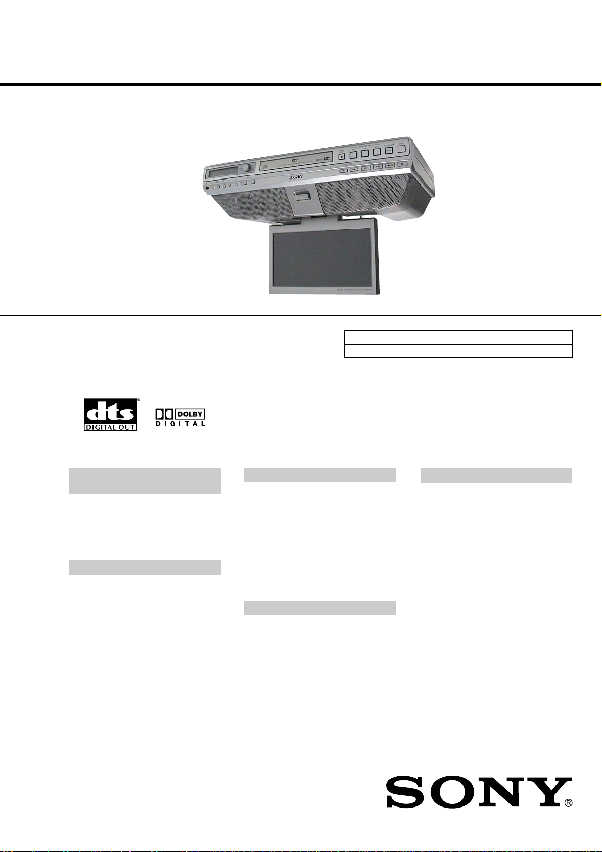
ICF-DVD57TV
General
Time display 12-hour system
Speaker 77 mm (3
1
⁄8 inches) dia,
6 Ω
Power outputs 1.8 W + 1.8 W (at 10%
harmonic distortion)
Power requirements 120 V AC, 60 Hz
Dimensions Approx. 400 × 123 × 322.5
mm (w/h/d)
(Approx. 15
3
⁄4 × 4 7⁄8 × 12 3⁄
4
inches) incl. projecting
parts and controls
Mass Approx. 4.8 kg (10 lb 9 oz)
Supplied accessories Mounting screws (4),
Template (1),
Spacers (4),
Remote control (1)
Design and specifications are subject to change
without notice.
DVD/CD player section
Emission duration Continuous
Laser output Less than 1,000 µW
(This output is the value
measured at a distance of
about 200 mm from the
objective lens surface on
the optical pick-up block
with 7 mm aperture.)
Frequency response: CD: 20 – 20,000 Hz +1/-1
dB
DVD Video: 20 – 22,000 Hz
+1/-1 dB
Wow and flutter: Below measurable limit
Output OPTICAL OUTPUT
Radio section
Frequency range FM : 87.5 – 108 MHz
AM: 530 – 1,710 kHz
SERVICE MANUAL
Ver. 1.0 2005.04
Manufactured under license from Dolby
Laboratories. “Dolby”, “Pro Logic”, and the
double-D symbol are trademarks of Dolby
Laboratories.
“DTS,” “DTS Digital Surround” and “DTS
Digital Out” are trademarks of Digital Theater
Systems, Inc.
US Model
Model Name Using Similar Mechanism NEW
Optical Pick-up Block Name KHM-310BAA
AUDIO POWER
SPECIFICATIONS
POWER OUTPUT AND TOTAL HARMONIC
DISTORTION
With 6–ohm loads, both channels driven from
100 – 10 000 Hz; rated 1.4 W per channelminimum RMS power, with no more than 10
% total harmonic distortion in AC operation.
TV section
Television system American TV standard/
Channel coverage VHF: 2–13/UHF: 14–69/
Antenna 75-ohm external antenna
Screen type Wide LCD color monitor
Size 9 inches
System TFT active matrix
Number of dots 336,960 dots
Input 1 video, 1 audio
9-879-703-01
2005D05-1
© 2005.04
NTSC
CATV: 1–125
terminal for VHF/UHF
Sony Corporation
Personal Audio Group
Published by Sony Engineering Corporation
SPECIFICATIONS
LCD-TV DVD KITCHEN CLOCK RADIO
ICF-DVD57TV
r
Discs that this system cannot play
•CD-ROMs
•CD-Rs/CD-RWs other than those recorded in
the following formats:
— music CD format
— video CD format
•Data part of CD-Extras
•Super Audio CDs
•DVD-ROMs
•DVD-RAMs
•DVD Audio discs
•8 cm(3 inches) DVD discs
•Photo Movies created after recording in VR
mode by DVD Handycam.
•Progressive JPEG format file
•Discs with non-standard shapes (e.g., heart,
square, star) cannot be played on this unit.
Attempting to do so may damage the unit.
Do not use such discs.
•A disc with paper or stickers on it
•A disc that has the adhesive, cellophane tape,
or a sticker still left on it.
* A logical format of files and folders on a CD-
ROMs, defined by ISO (International
Organization for standardization).
Notes on chip component replacement
• Never reuse a disconnected chip component.
• Notice that the minus side of a tantalum capacitor may be
damaged by heat.
Flexible Circuit Board Repairing
• Keep the temperature of the soldering iron around 270 ˚C
during repairing.
• Do not touch the soldering iron on the same conductor of the
circuit board (within 3 times).
• Be careful not to apply force on the conductor when soldering
or unsoldering.
SAFETY CHECK-OUT
After correcting the original service problem, perform the following
safety check before releasing the set to the customer:
Check the antenna terminals, metal trim, “metallized” knobs, screws,
and all other exposed metal parts for AC leakage.
Check leakage as described below.
LEAKAGE TEST
The AC leakage from any exposed metal part to earth ground and
from all exposed metal parts to any exposed metal part having a
return to chassis, must not exceed 0.5 mA (500 microamperes).
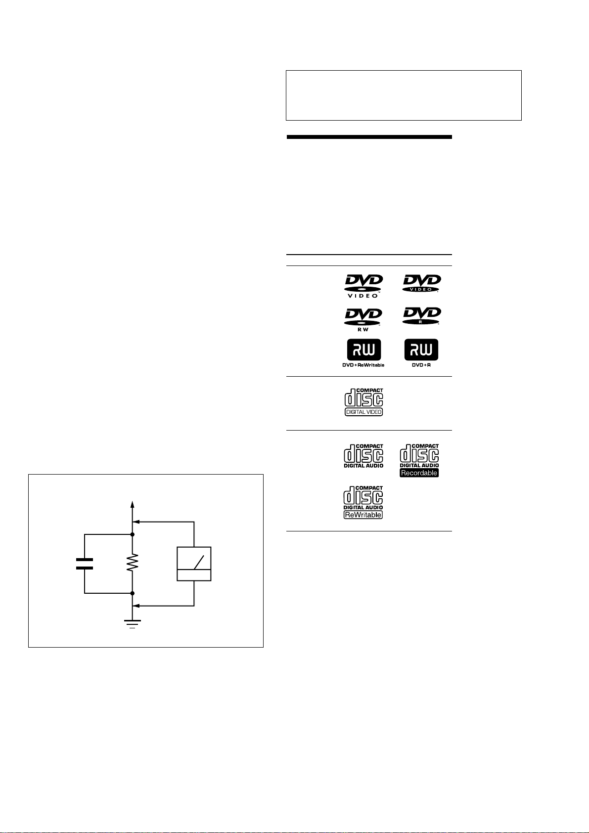
Leakage current can be measured by any one of three methods.
1. A commercial leakage tester, such as the Simpson 229 or RCA
WT -540A. Follow the manuf acturers’ instructions to use these
instruments.
2. A battery-operated A C milliammeter . The Data Precision 245
digital multimeter is suitable for this job.
3. Measuring the voltage drop across a resistor by means of a
VOM or battery-operated A C voltmeter . The “limit” indication
is 0.75 V, so analog meters must have an accurate low-v oltage
scale. The Simpson 250 and Sanwa SH-63Trd are examples
of a passive VOM that is suitable. Nearly all battery operated
digital multimeters that have a 2 V A C range are suitable. (See
Fig. A)
CAUTION
Use of controls or adjustments or performance of procedures
other than those specified herein may result in hazardous radiation
exposure.
About the discs this unit
can play
This unit can play the following discs:
•DVD VIDEO
•DVD-R/DVD+R
•DVD-RW/DVD+RW
•Video CD
•Audio CD
•CD-R/CD-RW
Disc type Label on the disc
DVD Videos
Video CD
Audio CDs
To Exposed Metal
Parts on Set
1.5 k
0.15 µF
Ω
Fig. A. Using an AC voltmeter to check AC leakage.
SAFETY-RELATED COMPONENT WARNING!!
COMPONENTS IDENTIFIED BY MARK 0 OR DOTTED LINE
WITH MARK 0 ON THE SCHEMATIC DIAGRAMS AND IN
THE PARTS LIST ARE CRITICAL TO SAFE OPERATION.
REPLACE THESE COMPONENTS WITH SONY P AR TS WHOSE
PART NUMBERS APPEAR AS SHOWN IN THIS MANU AL OR
IN SUPPLEMENTS PUBLISHED BY SONY.
2
Earth Ground
AC
voltmete
(0.75 V)
“DVD VIDEO,” “DVD-R” and “DVD-RW” are
trademarks.
ICF-DVD57TV
Notes about CD-R/CD-RW/DVD-R/
DVD-RW/DVD+R/DVD+RW
•In some cases, CD-Rs, CD-RWs, DVD-Rs,
DVD-RWs, DVD+Rs or DVD+RWs cannot be
played on this system depending upon the
recording quality or physical condition of the
disc, or the characteristics of the recording
device. Furthermore, the disc will not play if
it has not been correctly finalized. For more
information, see the operating instructions
for the recording device.
•A disc recorded in packet write format
cannot be played.
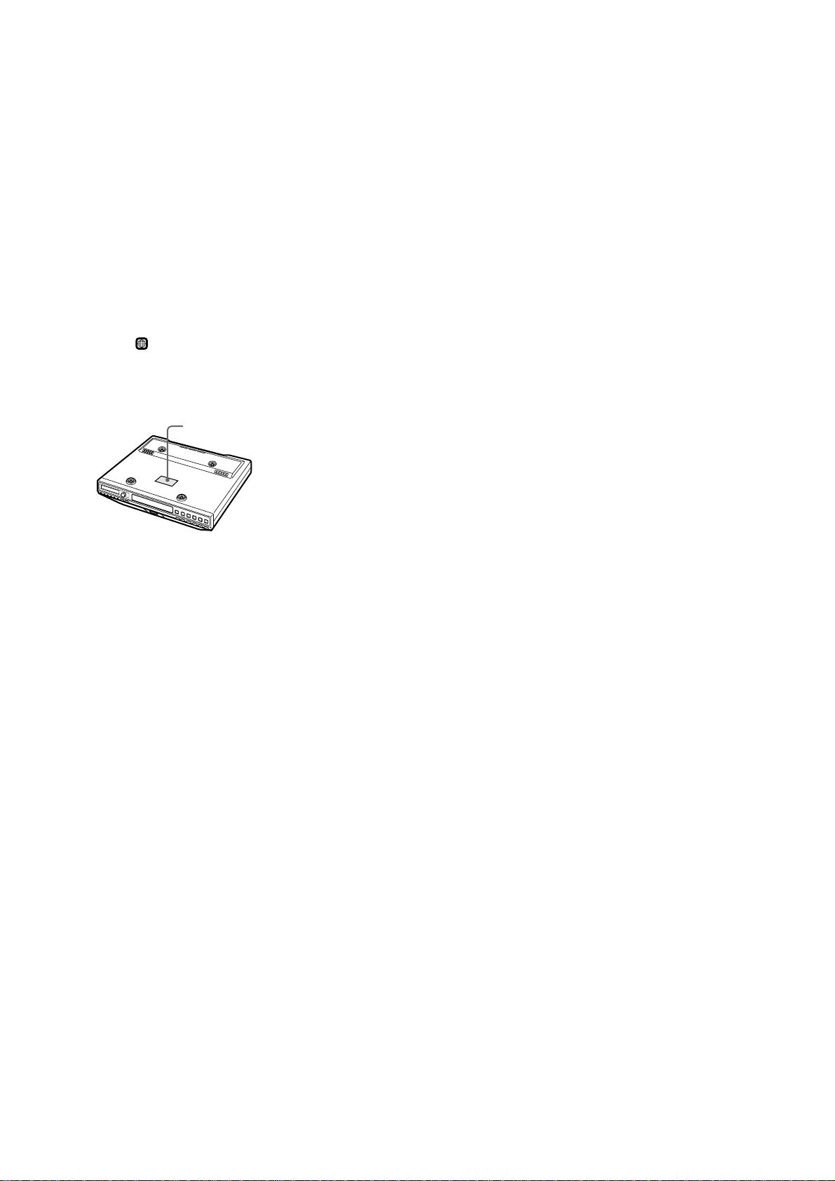
DVD region code this unit can play.
This unit has a region code printed on the top
of the unit and will only play DVDs that are
labeled with identical region codes. DVDs
labeled
If you try to play any other DVD, the message
“WRONG REGION” will appear on the screen.
Depending on the DVD, the region code
indication may not appear even if the DVD is
prohibited by area restrictions.
ALL
will also be played on this unit.
Region code
Note on DTS*-encoded DVDs/CDs
To enjoy DTS Digital Surround™ playback, an
external 5.1-channel DTS Digital Surround™
decoder system must be connected to the
digital output of this unit.
* “DTS,” “DTS Digital Surround” and “DTS Digital
Out” are trademarks of Digital Theater Systems,
Inc.
TABLE OF CONTENTS
1. SERVICING NOTES ............................................... 4
2. GENERAL ................................................................... 5
3. DISASSEMBLY
3-1. Disassembly Flow ........................................................... 6
3-2. Cabinet (Upper), Tray Lid Assy ...................................... 7
3-3. Mechanical Deck Assy .................................................... 7
3-4. Cabinet (Front) Assy ....................................................... 8
3-5. DVD Board...................................................................... 8
3-6. MAIN Board.................................................................... 9
3-7. Monitor Assy ................................................................... 9
3-8. Cabinet (Disp Rear)......................................................... 10
3-9. Shield (Disp).................................................................... 10
3-10. MONITOR Board,
Liquid Crystal Display Panel (LCD1)............................. 11
3-11. Belt, Tray ......................................................................... 12
3-12. Optical Pick-up KHM-310BAA...................................... 12
4. TEST MODE.............................................................. 13
5. ELECTRICAL ADJUSTMENTS ......................... 16
6. DIAGRAMS
6-1. Block Diagram – DVD Section – .................................... 22
6-2. Block Diagram – TUNER Section – ............................... 23
6-3. Block Diagram – AUDIO/PANEL Section – .................. 24
6-4. Block Diagram – MONITOR Section –.......................... 25
6-5. Block Diagram – POWER SUPPLY Section –............... 26
6-6. Printed Wiring Board – DVD Board (Side A) – .............. 28
6-7. Printed Wiring Board – DVD Board (Side B) –.............. 29
6-8. Schematic Diagram – DVD Board (1/2) – ...................... 30
6-9. Schematic Diagram – DVD Board (2/2) – ...................... 31
6-10. Printed Wiring Board – TU Board –................................ 32
6-11. Schematic Diagram – TU Board – .................................. 33
6-12. Printed Wiring Board
– MAIN Board (Component Side) – ............................... 34
6-13. Printed Wiring Board
– MAIN Board (Conductor Side) – ................................. 35
6-14. Schematic Diagram – MAIN Section (1/4) – .................. 36
6-15. Schematic Diagram – MAIN Section (2/4) – .................. 37
6-16. Schematic Diagram – MAIN Section (3/4) – .................. 38
6-17. Schematic Diagram – MAIN Section (4/4) – .................. 39
6-18. Printed Wiring Board – LCD Board –............................. 40
6-19. Printed Wiring Boards – SWITCH/TRANS Section ...... 41
6-20. Printed Wiring Board
– MONITOR Board (Component Side) – ....................... 42
6-21. Printed Wiring Board
– MONITOR Board (Conductor Side) – ......................... 43
6-22. Schematic Diagram – MONITOR Board (1/3) – ............ 44
6-23. Schematic Diagram – MONITOR Board (2/3) – ............ 45
6-24. Schematic Diagram – MONITOR Board (3/3) – ............ 46
7. EXPLODED VIEWS
7-1. Cabinet (Upper) Section.................................................. 70
7-2. Cabinet (Front) Section ................................................... 71
7-3. Cabinet (Lower) Section-1 .............................................. 72
7-4. Cabinet (Lower) Section-2 .............................................. 73
7-5. Monitor Section............................................................... 74
7-6. Mechanical Deck Section................................................ 75
8. ELECTRICAL PARTS LIST................................ 76
3

ICF-DVD57TV
SECTION 1
SERVICING NOTES
NOTES ON HANDLING THE OPTICAL PICK-UP
BLOCK OR BASE UNIT
The laser diode in the optical pick-up block may suffer electrostatic break-down because of the potential difference generated
by the charged electrostatic load, etc. on clothing and the human
body.
During repair, pay attention to electrostatic break-down and also
use the procedure in the printed matter which is included in the
repair parts.
The flexible board is easily damaged and should be handled with
care.
NOTES ON LASER DIODE EMISSION CHECK
The laser beam on this model is concentrated so as to be focused
on the disc reflective surface by the objective lens in the optical
pick-up block. Therefore, when checking the laser diode emission, observe from more than 30 cm away from the objectiv e lens.
UNLEADED SOLDER
Boards requiring use of unleaded solder are printed with the leadfree mark (LF) indicating the solder contains no lead.
(Caution: Some printed circuit boards may not come printed with
the lead free mark due to their particular size)
: LEAD FREE MARK
Unleaded solder has the following characteristics.
• Unleaded solder melts at a temperature about 40 °C higher than
ordinary solder.
Ordinary soldering irons can be used but the iron tip has to be
applied to the solder joint for a slightly longer time.
Soldering irons using a temperature regulator should be set to
about 350 °C.
Caution: The printed pattern (copper foil) may peel away if the
heated tip is applied for too long, so be careful!
• Strong viscosity
Unleaded solder is more viscou-s (sticky, less prone to flow)
than ordinary solder so use caution not to let solder bridges occur such as on IC pins, etc.
• Usable with ordinary solder
It is best to use only unleaded solder but unleaded solder may
also be added to ordinary solder.
4
Location of controls
Connection
Use this hookup if you subscribe to a CATV
System that does not require a cable box.
Basic Connections
(Connecting CATV or an
Antenna)
Connecting directly to cable or an antenna
1
2
3
4
5
6
7
8
9
0
qa
qs
SECTION 2
GENERAL
qd
qf
qg
qh
qj
qk
ql
w;
wa
ws
wd
ICF-DVD57TV
This section is extracted from
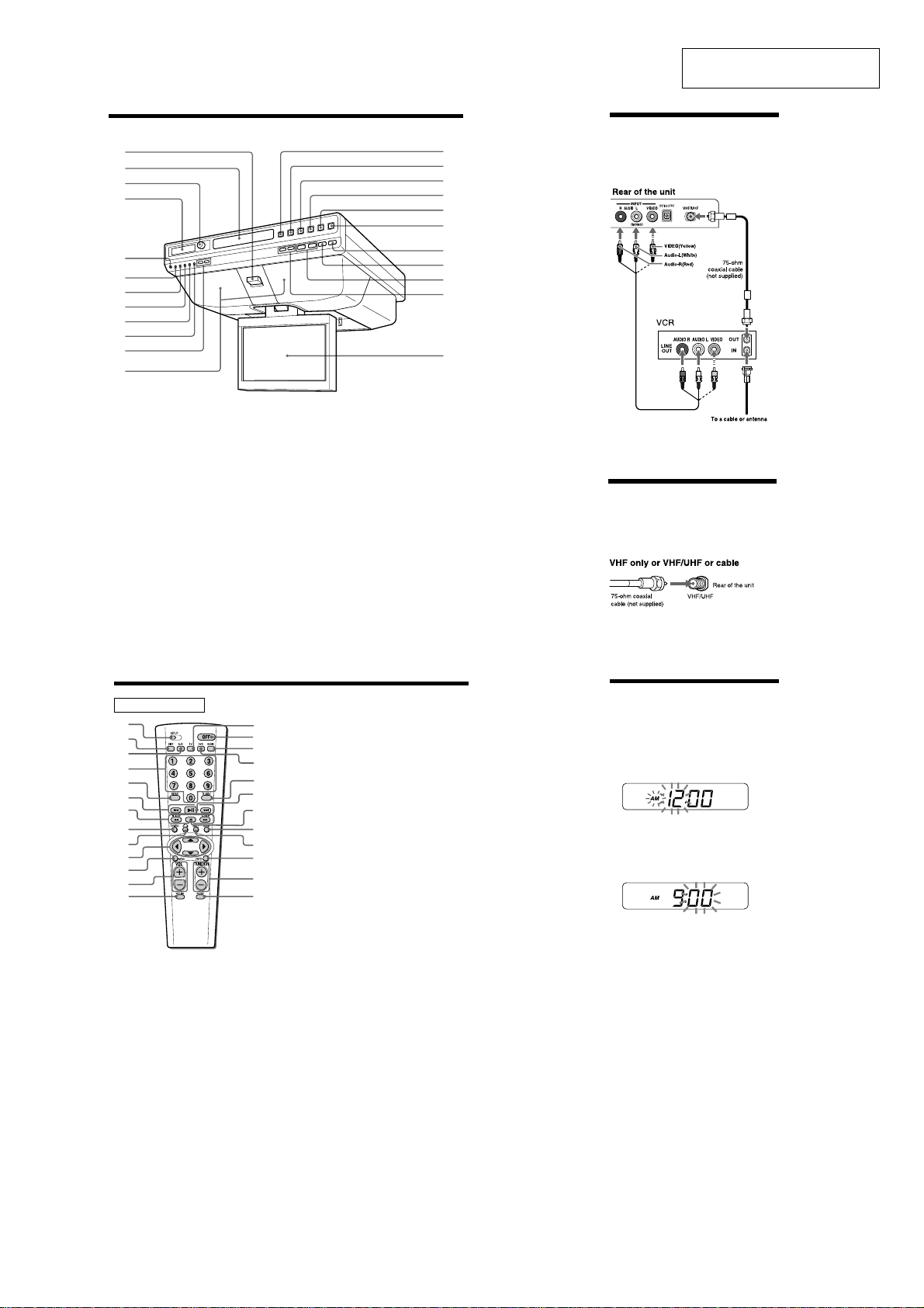
instruction manual.
Refer to the pages listed for details.
1 DISPLAY RELEASE
2 Disc Tray
3 TIMER dial and TIMER indicator, PUSH
START/STOP button
To operate the Cooking Timer.
4 Clock Display Window
5 Receptor for the remote control
6 CLOCK button
To set the clock.
7 MODE/SCREEN SIZE button
To set the screen mode, and to set the FM
mode.
8 TV MENU button
To change the screen settings.
9 ENTER button
0 SOUND button
To set the audio emphasis.
qa VOLUME +/– buttons
qs Speakers (left/right)
qd Z OPEN/CLOSE button
qf AUX button
To watch the AUDIO/VIDEO INPUT.
Remote control
1
2
3
4
5
6
7
8
9
0
qa
qs
qd
Refer to the pages listed for details.
1 SETUP button
Used to perform menu operations.
2 DISP (Display) button
To display the channel number or the time
information of the disc.
3 AUX button
To watch the AUDIO/VIDEO INPUT.
4 Number buttons
5 REPEAT button
To select the repeat mode (DVD/Video
CD/Audio CD).
6 .(Previous)/>(Next) buttons
7 tSLOW/m(Fast reverse)/TSLOW/M
(Fast forward) buttons
This can also be used in slow playback
mode.
8 TOP MENU button
To display the top menu of a recorded DVD,
or to set the PBC (playback control)
function on or off for the Video CD.
9 O (Return) button
q; v/V/b/B buttons
qa MENU button
To display the recorded DVD menu.
qs VOL (Volume) +/– buttons
qd MUTING button
To attenuate the volume.
* There is a tactile dot on the VOLUME + and
u buttons.
qg TV button
To turn on the TV.
qh DVD button
To turn on the player.
qj RADIO ON/BAND button
To turn on the radio.
To change the band (FM/AM).
qk OFF button
To turn off the AUX/TV/DVD/Radio
unit.
ql x (Stop) button
w; u (Play/Pause) button
wa TV CH/PRESET –, .(Previous)/
+ ,>(Next) button
To select a TV channel, to tune in a preset
station, to select the item during TV
MENU operation, or to adjust the screen
settings.
ws RADIO TUNE/TIME SET –, m(Fast
reverse)/+, M(Fast forward) button
To tune in a desired radio station or to set
the clock.
This can also be used in slow playback mode.
wd Monitor
qf
qg
qh
qj
The corresponding buttons of the
remote control function the same as
those on the unit.
Instructions in this manual describe how to use
the unit by mainly using the remote control.
qk
ql
w;
wa
ws
wd
wf
wg
* There is a tactile dot on the “5”, “u” and
“TUNE/CH+” buttons of the remote control.
qf TV button
To turn on the TV.
qg OFF button
To turn off the AUX/TV/DVD/Radio unit.
qh RADIO/BAND button
To turn on the radio.
qj DVD button
To turn on the unit.
qk TV MENU button
To change the screen settings.
ql u (Play/Pause) button
w; x (Stop) button
wa AUDIO button
To change the audio output/audio language.
ws ANGLE button
To select the multiple angles of view while
playing a DVD.
wd ENTER button
To enter a setting.
wf TUNE/CH +/– buttons
To select the desired TV channel, to tune in
to the desired station, to select the item
during TV MENU operation or to adjust
the screen settings.
wg SOUND button
To set the audio emphasis.
Setting the Clock
1
Plug in the unit.
“AM 12:00” will flash in the Clock Display
Window.
2
Press CLOCK for a few seconds.
You will hear a beep and the hour digits
will start to flash in the Clock Display
Window.
3
Press RADIO TUNE/TIME SET –, m(fast
reverse) or +, M(fast forward) until
the correct hour appears in the Clock
Display Window.
4
Press CLOCK (or ENTER) once.
The minute digits will flash.
5
Press RADIO TUNE/TIME SET –, m(fast
reverse) or +, M(fast forward) until
the correct minute appears in the Clock
Display Window.
6
Press CLOCK (or ENTER) once.
You will hear two short beeps and the
seconds start counting from zero.
Tips
• To set the current time rapidly, hold down
RADIO TUNE/TIME SET –, m(fast reverse) or +,
M(fast forward).
• To set the current time exactly to the seconds,
adjust the minute function in step 6 and then
press CLOCK (or ENTER) to synchronize it with a
time signal (such as the telephone time signal).
•In the 12-hour system: “AM 12:00” = midnight.
5
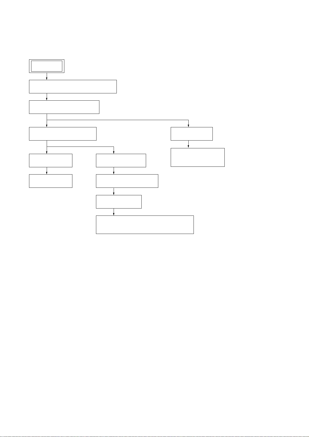
ICF-DVD57TV
• This set can be disassembled in the order shown below.
3-1. DISASSEMBLY FLOW
SET
3-2. CABINET (UPPER), TRAY LID ASSY
(Page 7)
3-3. MECHANICAL DECK ASSY
(Page 7)
SECTION 3
DISASSEMBLY
3-4. CABINET (FRONT) ASSY
(Page 8)
3-5. DVD BOARD
(Page 8)
3-6. MAIN BOARD
(Page 9)
3-7. MONITOR ASSY
(Page 9)
3-8. CABINET (DISP REAR)
(Page 10)
3-9. SHIELD (DISP)
(Page 10)
3-10. MONITOR BOARD,
LIQUID CRYSTAL DISPLAY PANEL (LCD1)
(Page 11)
3-11. BELT, TRA Y
(Page 12)
3-12. OPTICAL PICK-UP
KHM-310BAA
(Page 12)
6
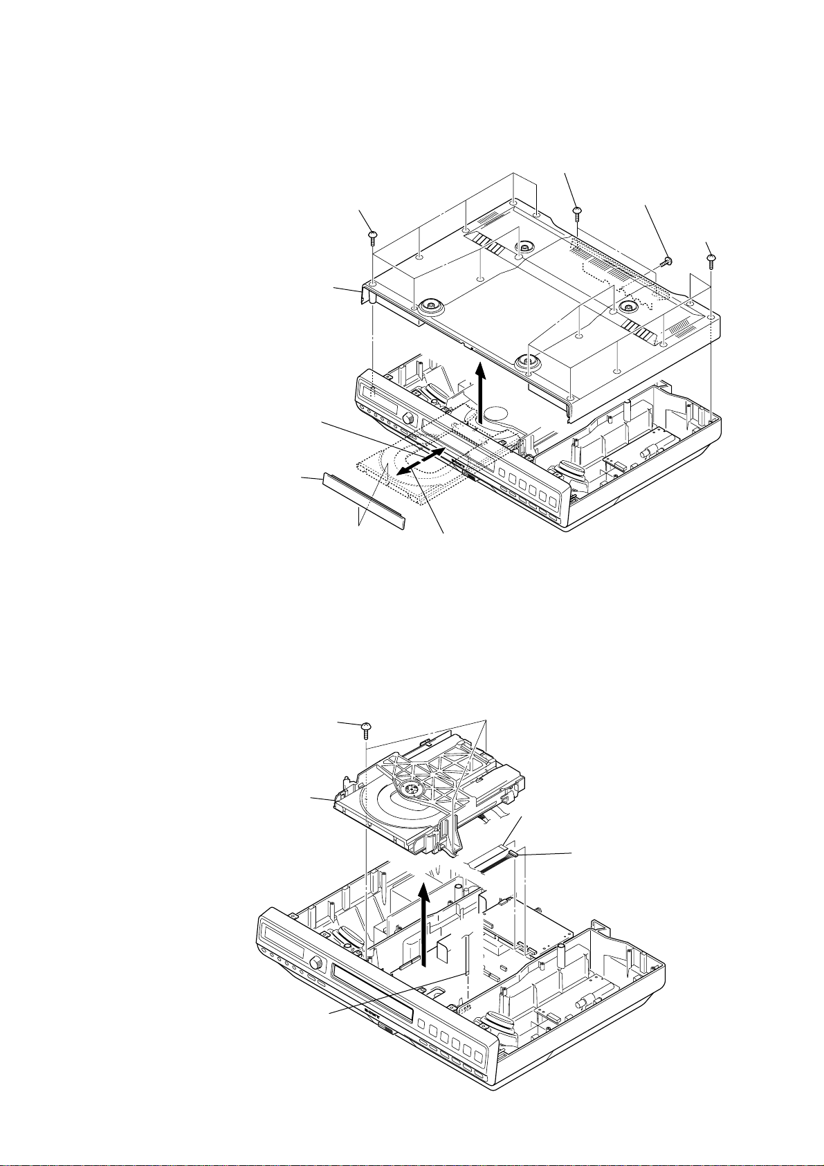
Note: Follow the disassembly procedure in the numerical order given.
s
3-2. CABINET (UPPER), TRAY LID ASSY
4
eight screws
(B3)
7
cabinet (upper)
3
Turn on the power supply, and press the
open/close button to close the tray.
6
4
two screws
(B3)
5
screw (B3)
ICF-DVD57TV
4
eight screw
(B3)
2
tray lid assy
3-3. MECHANICAL DECK ASSY
3
three screws
(B3)
6
mechanical deck assy
4
1
Turn on the power supply, and press the
open/close button to open the tray.
1
flexible flat (24 core) cable
(CN702)
2
connector
(CN703)
5
flexible flat (5 core) cable
(CN351)
7
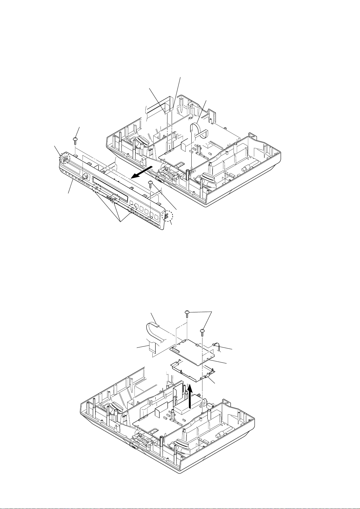
ICF-DVD57TV
r
3-4. CABINET (FRONT) ASSY
2
flexible flat (16 core) cable
(CN602)
4
two screws
(B2.6)
5
claw
1
flexible flat (12 core) cable
(CN601)
3
flexible flat (9 core) cable
(CN403)
6
cabinet (front) assy
3-5. DVD BOARD
5
three claws
2
flexible flat (8 core) cable
(CN704)
1
flexible flat (24 core) cable
(CN701)
5
4
two screws
(B2.6)
claw
4
four screws
(B2.6)
3
5
DVD board
connecto
(CN705)
6
shield (DVD lower)
8
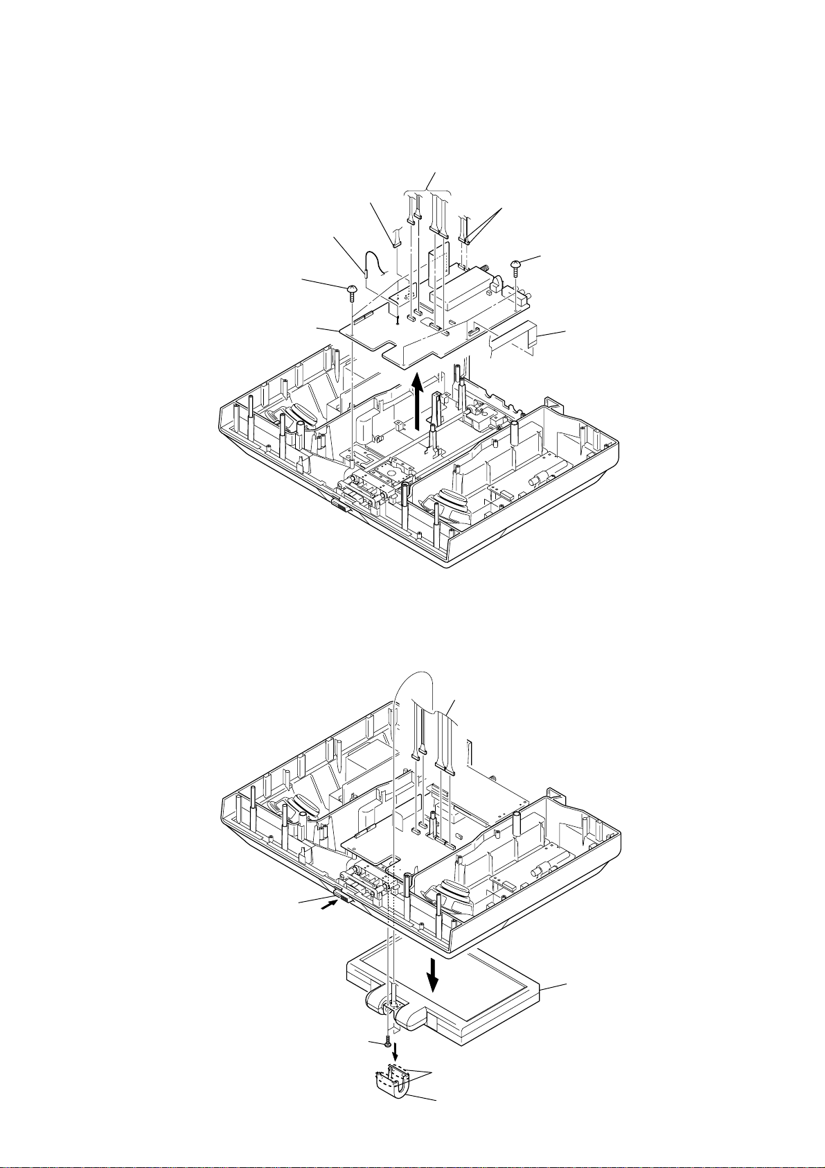
3-6. MAIN BOARD
e
4
three screws
(B2.6)
5
3
terminal
(CN902)
MAIN board
2
connector
(CN901)
2
four connectors
(CN403, CN404, CN405, CN406)
2
two connectors
(CN302, CN401)
4
three screws
(B2.6)
1
ICF-DVD57TV
flexible flat (11 core) cabl
(CN10)
3-7. MONITOR ASSY
5
Push the button (release).
4
four screws
1
four connectors
(CN403, CN404, CN405, CN406)
6
7
monitor assy
2
four claws
3
cover (shaft)
9
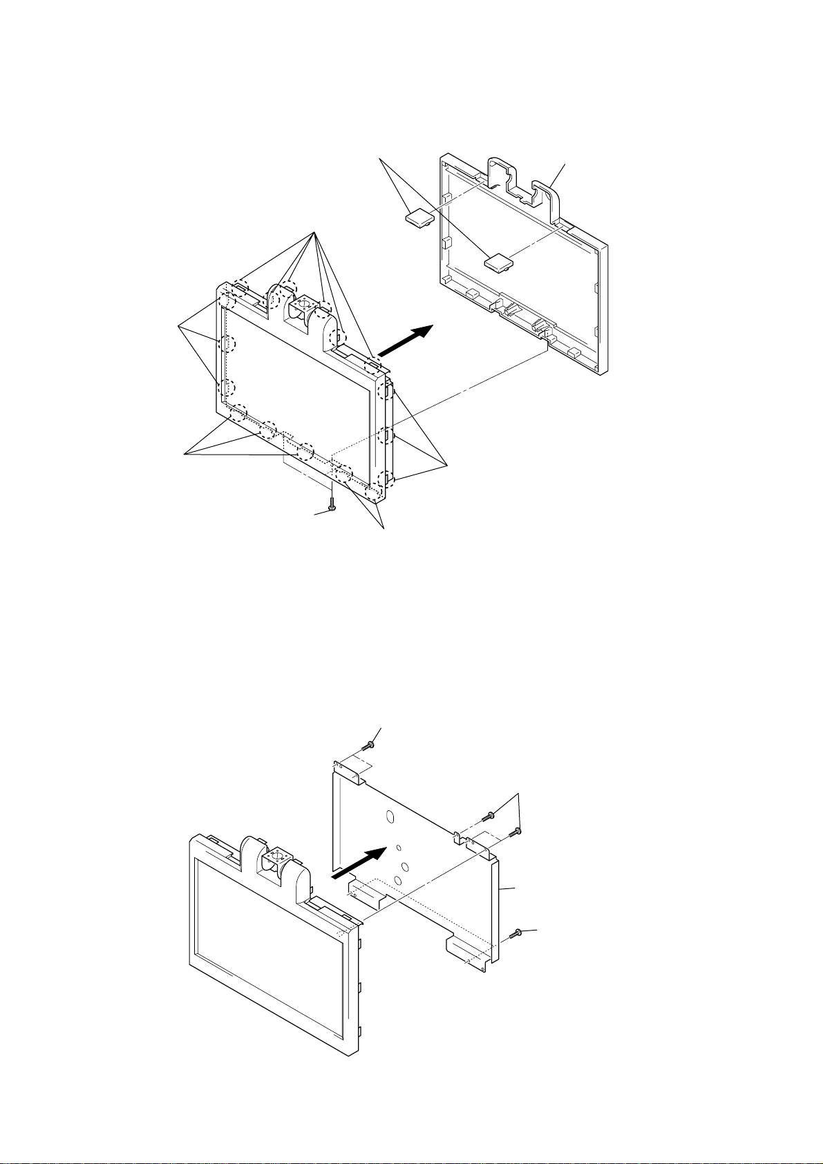
ICF-DVD57TV
)
s
3-8. CABINET (DISP REAR)
2
three claws
3
two sliders (DISP)
2
six claws
4
cabinet (DISP rear
2
three claws
3-9. SHIELD (DISP)
1
two screws
2
two claws
1
two screws
2
three claws
1
three screws
10
2
shield (DISP)
1
two screw
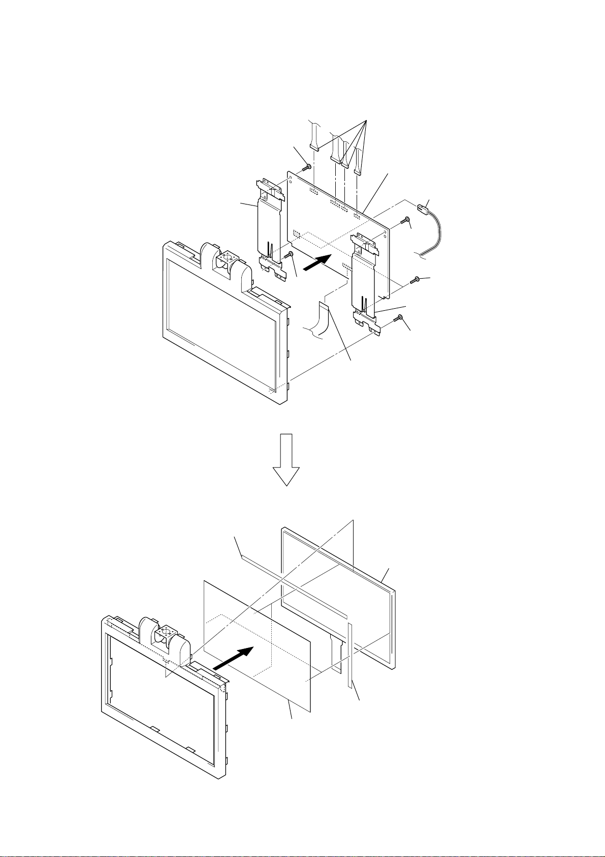
3-10. MONITOR BOARD, LIQUID CRYSTAL DISPLAY PANEL (LCD1)
)
1
four connectors
(CN1403, CN1404, CN1405, CN1406
4
screw
6
8
bracket (DISP)
7
screw
MONITOR board
2
connector
(CN1801)
4
screw
5
two screws
8
bracket (DISP)
ICF-DVD57TV
qa
two adhesive tapes
3
LCD flexible board
(CN1802)
qs
7
screw
liquid crystal display panel
(LCD1)
9
q;
panel (DISP)
qa
two adhesive tapes
11
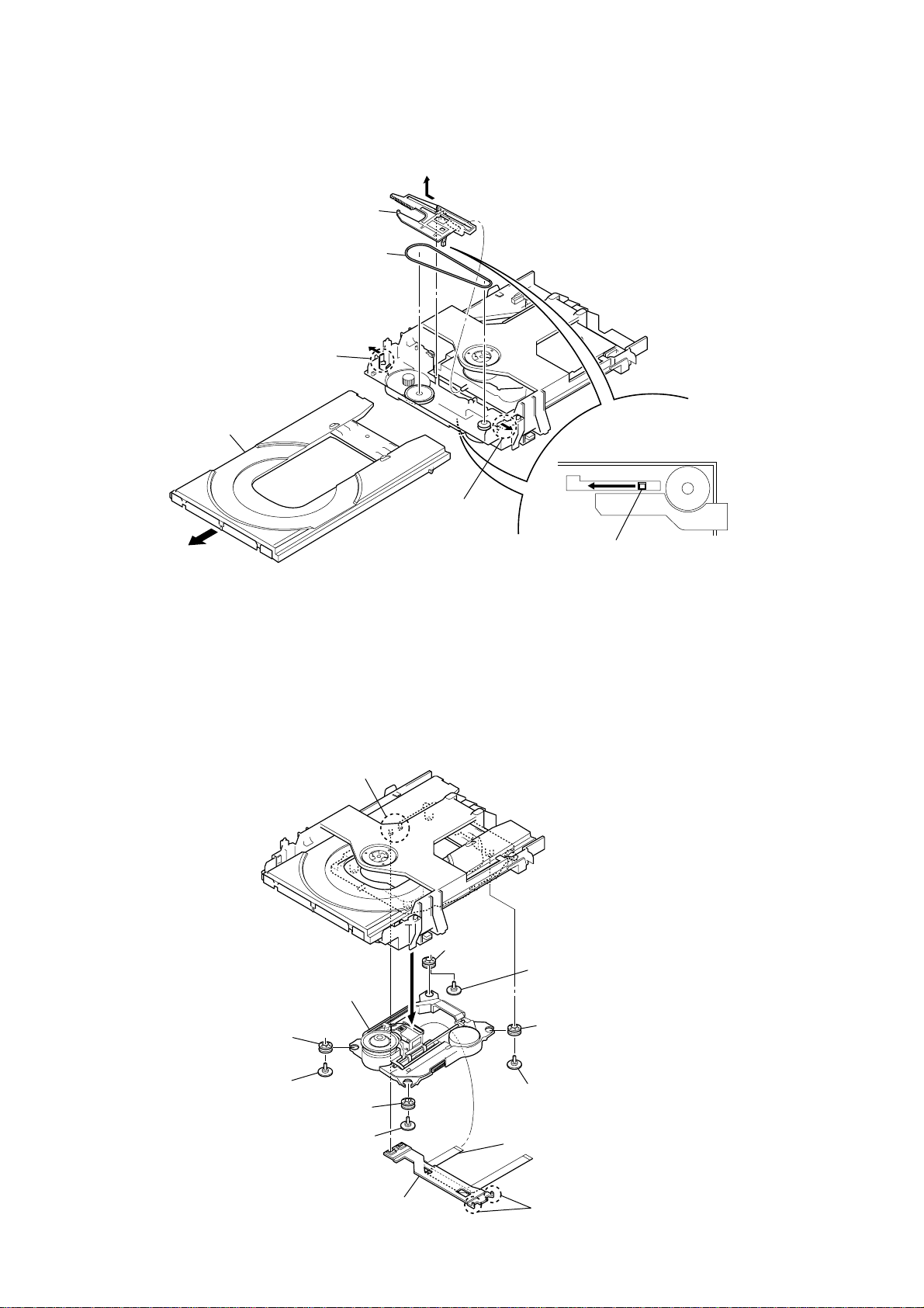
ICF-DVD57TV
3-11. BELT, TRAY
4
tray
3
5
claw
chuck cam
6
belt
2
3-12. OPTICAL PICK-UP KHM-310BAA
2
8
optical pick-up KHM-310BAA
two claws
6
3
7
claw
insulator
1
Slide the chuck cam in the direction
of arrow to releae the chucking.
5
insulator screw
12
7
5
insulator screw
insulator
5
7
insulator
insulator screw
4
holder (FFC)
7
insulator
5
insulator screw
1
flexible flat (24 core) cable
3
two claws
SECTION 4
TEST MODE
ICF-DVD57TV
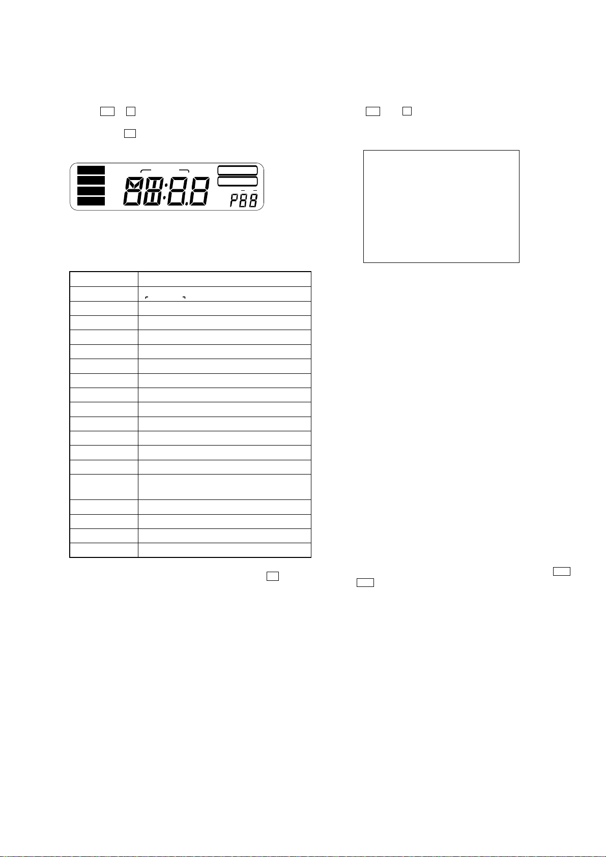
LCD TEST MODE
Procedure:
1. Turn the power on while pressing simultaneously three keys
of M , x and [TV MENU].
2. The microprocessor version will be displayed on the LCD.
3. Press the Z key. The LCD display will become as follows.
LCD display
RADIO
DVD
FM
TV
AM
PM
AUX
4. The display corresponding to a key is turned off, if a key on
the set is pressed.
TIMER
MEGABASS
MEGAXpand
MHz
kHz
VOL
Key Corresponding Table
Key Segment
TIMER TIMER , TIMER LED
CLOCK AM, PM, : (colon)
MODE 5a, 5d, MEGA EXPAND, P, kHz, MHz
TV MENU 6b, 6c, 6d, 6e, 6g, 5c, 5e
SOUND MEGA BASS
VOLUME – – VOL –
VOLUME + . (dot)
m 5f
M 6a
. 4a, 4d, 4e
> 1d, 1h, 1a, 1e, 1f, 1g
u 2c, 2f, 2h, 2i
x 3e, 3f
OFF 1b, 1c, 2a, 2b, 2d, 2e, 2g, 3a, 3b, 3c, 3d, 3g,
4b, 4c, 4f, 4g
BAND RADIO, FM
DVD DVD
TV TV
AUX AUX
5. After all keys on the set were pressed, press the Z key, and
the test mode will be released.
TV TEST MODE
Procedure:
1. Turn the power on while pressing simultaneously two keys
of M and x .
2. When the TV test mode is activated, the monitor will become
as follows.
SR7596 TEST MODE MENU
1. INITIAL MENU
2. FOR FACTORY
3. LCD SETTING
4. LOAD DEFAULT
5. TUNER TEST
SR7596 Ver. 1.00a
3. Five items can be changed over by pressing the [TV MENU]
key.
4. The selected item is displayed in red and the items not selected
are displayed in cyan. (“SR7596 Ver. 1.00a” is displayed in red.)
5. You can enter the selected item by pressing the [ENTER] key.
6. Also, an item can be selected directly with the [1] to [5] keys
on the remote commander (RMT-CDVD57A).
1. INITIAL MENU (TV MENU PRESET)
• TV menu item is initialized.
Procedure:
1. Press the [TV MENU] key to select the “INITIAL MENU” on
the main screen.
2. Each item of TV menu can be initialized, if pressing the
[ENTER] key.
2. FOR FACTORY (FOR ADJUSTMENT)
• It is used at the time of adjustment.
Procedure:
1. Press the [TV MENU] key to select the “FOR FACTORY” on
the main screen.
2. A changing between setting item and “EXIT” is possible by
pressing the [TV MENU] key. (The selected item is displayed
in red)
3. If the [ENTER] key is pressed when the setting item has been
selected, settable items can be changed over , and the value of
the selected item can be adjusted by pressing the ./
keys. (For details, refer to VIDEO B US ADJUSTMENT
>
(See page 19))
4. The main screen comes back if the [ENTER] key is pressed
when “EXIT” has been selected.
Note: The same operation is also carried out by pressing the keys
on the remote commander.
3. LCD SETTING
This mode is not used in servicing.
4. LOAD DEFAULT
• It carries out, only when EEPROM (IC1451) is exchanged.
Procedure:
1. Press the [TV MENU] key to select the “LOAD DEFAUL T” on
the main screen.
2. All settings can be initialized, if pressing the [ENTER] key.
(In addition to the “INITIAL MENU”, set value of RGB
decoder (IC1501) and tuner N value)
5. TUNER TEST
This mode is not used in servicing.
13
ICF-DVD57TV
p
DVD TEST MODE
Procedure:
1. Turn the power on and press the [DVD] key to select the “D VD”.
2. Press the Z key to open the disc tray.
3. Press the key on the remote commander (RMT-CDVD57A)
as following order.
[TOPMENU] → [ANGLE] → [MENU] → [AUDIO]
4. When the test mode is activated, the monitor will become as
follows.
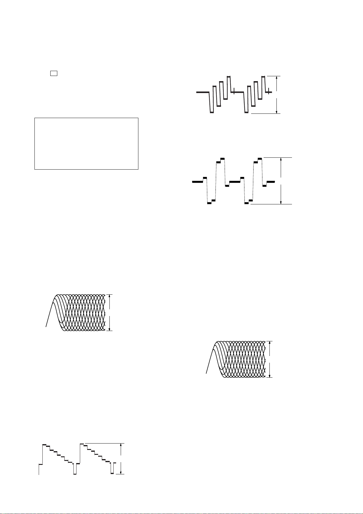
15. Connect the oscilloscope to TP708 and TP709 on the DVD
board.
16. Check that the oscilloscope waveform of B-Y signal is as
shown in the figure below.
1.45 ± 0.1 Vp-p
SR-7596 TEST MODE
JITTER VALUE – —
RF LEVEL – —
TRACKING ERROR AMP – —
FOCUS ERROR AMP – —
TRK SERVO GAIN AUTO ADJ – —
FCS SERVO GAIN AUTO ADJ – —
1. DVD OPERATION CHECK
Procedure:
1. Insert the DVD test disc (TDV-540C) (Part No. J-2501-235A) to start the automatic adjustment for DVD.
2. Connect the multi meter to TP753 and TP751 on the DVD
board.
3. Check that the reading of multi meter is 40 to 75 mA.
4. Check that the JITTER VALUE of monitor is 2D5 to 000
HEX.
5. Connect the oscilloscope to TP761 and TP702 on the DVD
board.
6. Check that the RF LEVEL of monitor is B8 to 87 HEX.
7. Check that the oscilloscope waveform of RF signal is as shown
in the figure below. (eye pattern)
A good eye pattern means that the diamond shape (◊) in the
center of the waveform can be clearly distinguished.
550 ± 100 mVp-p
17. Connect the oscilloscope to TP710 and TP711 on the DVD
board.
18. Check that the oscilloscope waveform of R-Y signal is as
shown in the figure below.
1.45 ± 0.1 Vp-p
2. CD OPERATION CHECK
Procedure:
1. Insert the CD test disc (PATD-012) (Part No. 4-225-203-01)
to start the automatic adjustment for CD.
2. Connect the multi meter to TP753 and TP752 on the DVD
board.
3. Check that the reading of multi meter is 55 to 85 mA.
4. Check that the JITTER VALUE of monitor is 2BC to 000
HEX.
5. Connect the oscilloscope to TP761 and TP702 on the DVD
board.
6. Check that the RF LEVEL of monitor is A5 to 70 HEX.
7. Check that the oscilloscope waveform of RF signal is as shown
in the figure below. (eye pattern)
A good eye pattern means that the diamond shape (◊) in the
center of the waveform can be clearly distinguished.
8. Check that the TRACKING ERROR AMP of monitor is EB
to 8C HEX.
9. Check that the FOCUS ERROR AMP of monitor is FF to BE
HEX.
10. Check that the TRK SERVO GAIN ADJ of monitor is 56 to
38 HEX.
11. Check that the FOCU SERV O GAIN ADJ of monitor is 42 to
18 HEX.
12. Insert the DVD test disc (HLX-N1) (Part No. 8-797-000-10)
and play the title5-chapter2 (full color bar 100%).
13. Connect the oscilloscope to TP706 and TP707 on the DVD
board.
14. Check that the oscilloscope waveform of Y signal is as shown
in the figure below.
1.0 ± 0.1 Vp-
14
700 ± 200 mVp-p
8. Check that the TRACKING ERROR AMP of monitor is BA
to 6E HEX.
9. Check that the FOCUS ERROR AMP of monitor is FF to B9
HEX.
10. Check that the TRK SERVO GAIN ADJ of monitor is 4F to
32 HEX.
11. Check that the FOCU SERVO GAIN ADJ of monitor is 52 to
37 HEX.

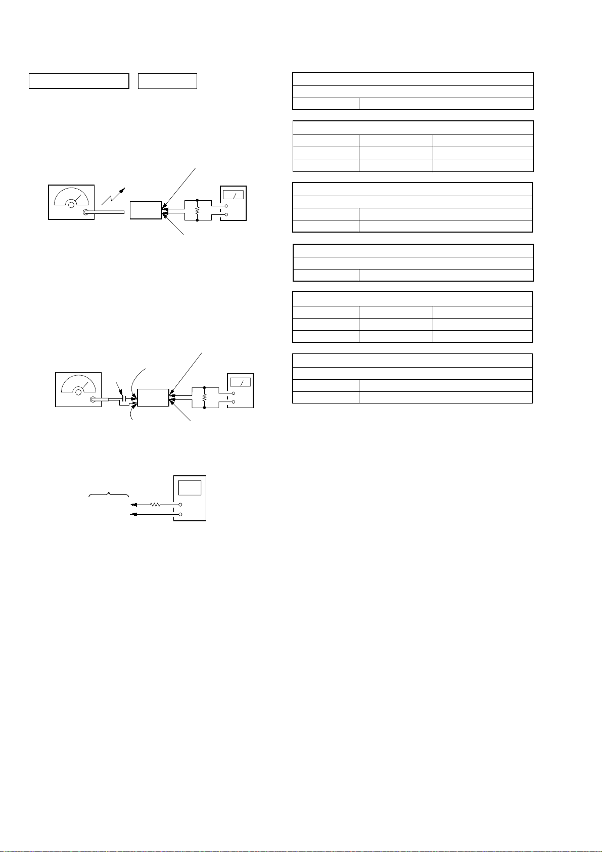
Connecting Location:
– DVD BOARD (Side B) –
ICF-DVD57TV
TP752
TP709
TP711
TP707
TP710
TP706
TP708
TP702
TP761
TP751
TP753
15
ICF-DVD57TV
r
SECTION 5
ELECTRICAL ADJUSTMENTS
TUNER SECTION 0 dB=1 µV
[AM]
Setting:
Function: RADIO
Band: AM
AM RF signal
generator
30% amplitude
modulation by
400 Hz signal
Output level:
as low as possible
[FM]
Setting:
Function: RADIO
Band : FM
FM RF signal
generator
22.5 kHz frequency
deviation by 400 Hz
signal
Output level:
as low as possible
Put the lead-wire
antenna close to
the set.
set
TU board
TP (ANT)
0.01 µF
set
TU board
TP (GND)
MAIN board
CN302 pin
level meter
6
Ω
MAIN board
CN302 pin
MAIN board
CN302 pin
6
Ω
MAIN board
CN302 pin
1
+
–
2
1
level meter
+
–
2
AM IF ADJUSTMENT
Adjust for a maximum reading on level meter
T1 450 kHz
AM VCO VOL TAGE ADJUSTMENT
Adjustment Part Frequency Display Reading on Digital Voltmeter
Confirmation 530 kHz 1.0 ± 0.1 V
L4 1,710 kHz 5.3 ± 0.7 V
AM TRACKING ADJUSTMENT
Adjust for a maximum reading on level meter
L3 620 kHz
CT3 1,400 kHz
FM IF ADJUSTMENT
Adjust for a minimum reading on level meter
T2 10.7 MHz
FM VCO VOL TAGE ADJUSTMENT
Adjustment Part Frequency Display Reading on Digital Voltmeter
Confirmation 87.5 MHz 1.3 ± 0.2 V
L2 108 MHz 3.0 ± 0.2 V
FM TRACKING ADJUSTMENT
Adjust for a maximum reading on level meter
L1 87.5 MHz
CT1 108 MHz
Adjustment and Connecting Location:
TU board (See page 17)
digital voltmete
TU board
Ω
TP (VT)
100 k
TP (GND)
• Repeat the procedures in each adjustment several times, and
the tracking adjustments should be finally done by the trimmer
capacitors.
16
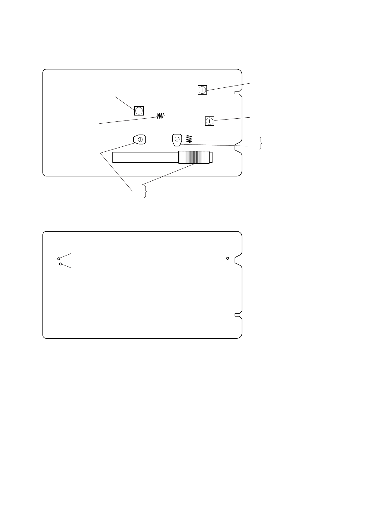
Adjustment and Connecting Location:
– TU BOARD (Component Side) –
ICF-DVD57TV
AM VCO Voltage Adjustment
L4
L2
FM VCO Voltage Adjustment
– TU BOARD (Conductor Side) –
TP
(VT)
L3
AM T rac king Adjustment
CT3
TP
(ANT)
T2 FM IF Adjustment
T1 AM IF Adjustment
L1
FM T rac king Adjustment
CT1
TP
(GND)
17
ICF-DVD57TV
)
)
)
)
)
)
)
)
MONITOR SECTION
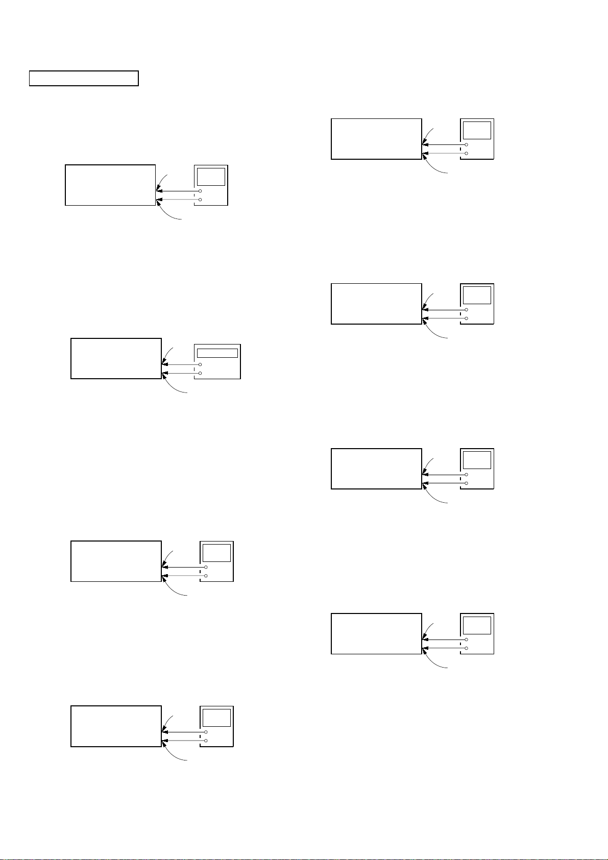
5-1. VOL TAGE AND FREQUENCY ADJUSTMENT
5-1-1. 5.0V Adjustment
Connection:
digital
voltmeter
TP1907
set
+
–
TP1901 (GND
Adjustment Procedure:
1. Connect a digital voltmeter to the TP1907 and TP1901 (GND)
on the MONITOR board.
2. Adjust the RV1901 so that the reading of digital voltmeter is
5.0 ± 0.1 V.
5-1-1. DC/DC Converter Frequency Adjustment
Connection:
frequency
TP1906
set
counter
+
–
TP1901 (GND
Adjustment Procedure:
1. Connect a frequency counter to the TP1906 and TP1901
(GND) on the MONITOR board.
2. Adjust the RV1902 so that the reading of frequenc y counter is
243 ± 1 kHz.
5-2. VOLTAGE CHECK
5-2-3. VSS (–13.0V) Check
Connection:
digital
voltmeter
TP1951
set
+
–
TP1901 (GND
Checking Procedure:
1. Connect a digital voltmeter to the TP1951 and TP1901 (GND)
on the MONITOR board.
2. Check that the reading of digital voltmeter is –12.0 ± 1.0 V.
5-2-4. 7.5V Check
Connection:
digital
voltmeter
TP1909
set
+
–
TP1901 (GND
Checking Procedure:
1. Connect a digital voltmeter to the TP1909 and TP1901 (GND)
on the MONITOR board.
2. Check that the reading of digital voltmeter is 7.4 ± 0.2 V.
5-2-5. 3.9V Check
Connection:
digital
voltmeter
TP1421
set
+
–
5-2-1. VDD (3.3V) Check
Connection:
digital
voltmeter
TP1954
set
+
–
TP1901 (GND
Checking Procedure:
1. Connect a digital voltmeter to the TP1954 and TP1901 (GND)
on the MONITOR board.
2. Check that the reading of digital voltmeter is 3.1 ± 0.2 V.
5-2-2. VGH (17.0V) Check
Connection:
digital
voltmeter
TP1952
set
+
–
TP1901 (GND
Checking Procedure:
1. Connect a digital voltmeter to the TP1952 and TP1901 (GND)
on the MONITOR board.
2. Check that the reading of digital voltmeter is 16.8 ± 1.0 V.
TP1901 (GND
Checking Procedure:
1. Connect a digital voltmeter to the TP1421 and TP1901 (GND)
on the MONITOR board.
2. Check that the reading of digital voltmeter is 3.85 ± 0.2 V.
5-2-6. Inverter V oltage Check
Connection:
digital
voltmeter
TP1412
set
+
–
TP1901 (GND
Checking Procedure:
1. Connect a digital voltmeter to the TP1412 and TP1901 (GND)
on the MONITOR board.
2. Check that the reading of digital voltmeter is 8.0 ± 0.2 V.
18
ICF-DVD57TV
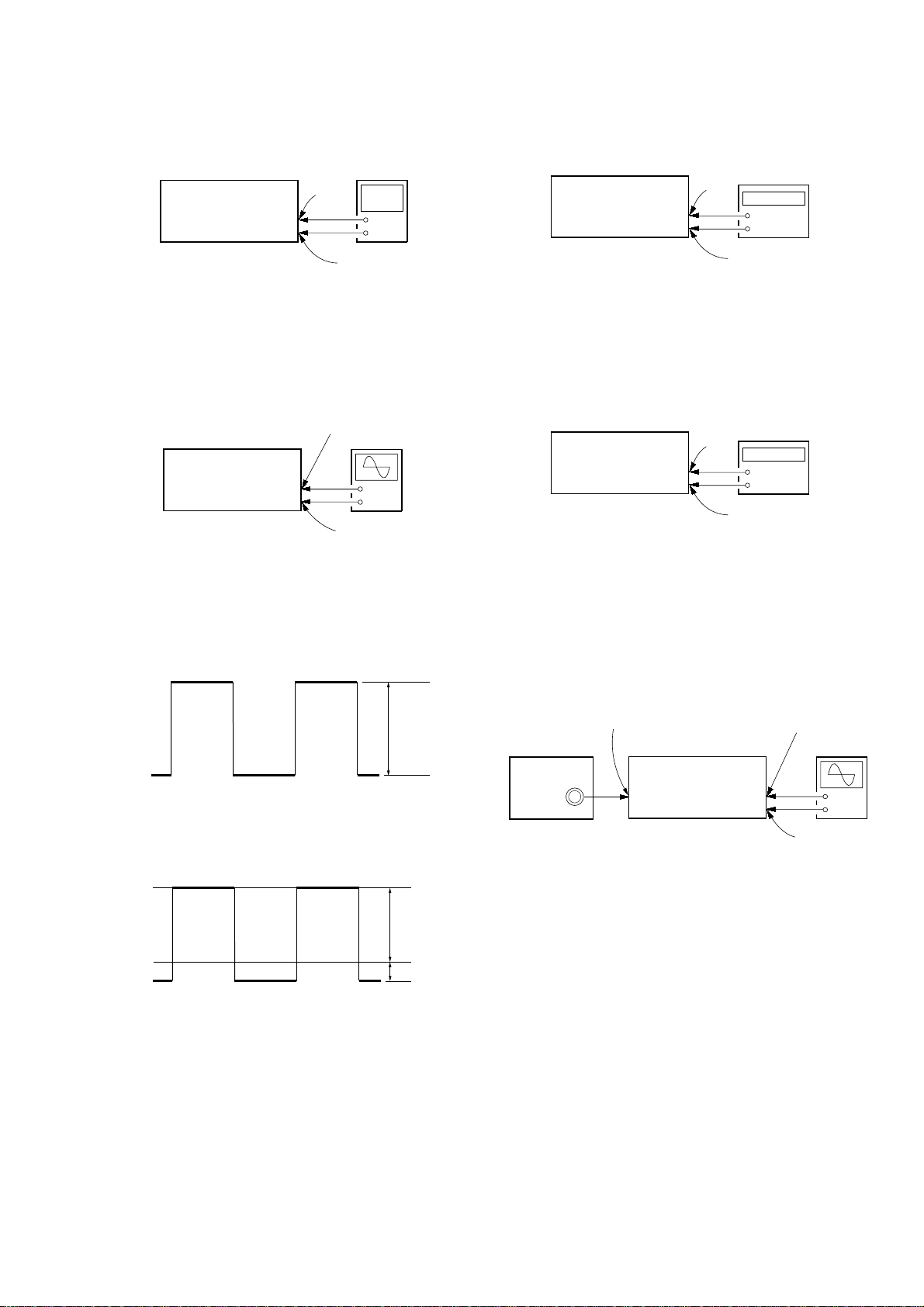
)
V
5-3. PLL ADJUSTMENT
Connection:
digital
voltmeter
TP1651
set
+
–
TP1901 (GND
Adjusting Procedure:
1. Connect a digital voltmeter to the TP1651 and TP1901 (GND)
on the MONITOR board.
2. Adjust the RV1651 so that the reading of digital voltmeter is
2.2 ± 0.15 V.
5-4. V COM ADJUSTMENT
Connection:
TP1960
osclloscope
set
Adjusting Procedure:
Connect an oscilloscope to the TP1960 and TP1901 (GND) on the
MONITOR board.
5-4-1. Voltage Set Up Adjustment
Adjust the set so that the A level of the waveform on the oscilloscope
is 6.6 ± 0.1 Vp-p. (Refer to the 5-7. video bus adjustment)
+
–
TP1901 (GND)
5-5. OSD DOT CLOCK CHECK
Connection:
frequency counter
(high impedance probe)
TP1515
set
+
–
TP1901 (GND)
Adjusting Procedure:
1. Connect an frequency counter to the TP1515 and TP1901
(GND) on the MONITOR board.
2. Check that the reading of frequency counter is 6.5 ± 0.2 MHz.
5-6. NTSC SUB CARRIER CHECK
Connection:
frequency counter
(high impedance probe)
TP1510
set
+
–
TP1901 (GND)
Checking Procedure:
1. Connect an frequency counter to the TP1510 and TP1901
(GND) on the MONITOR board.
2. Check that the reading of frequency counter is 3.579545 MHz
± 100 Hz.
5-7. VIDEO BUS ADJUSTMENT
Connection: (5-7-1 to 5-7-9)
A
5-4-2. Position Set Up Adjustment
Check the B lev el of the wav eform on the oscilloscope is 4.7 ± 0.1
Vp-p and adjust the RV1501 so that the C level of the waveform
on the oscilloscope is –1.9 ± 0.1 Vp-p.
B
0
C
INPUT VIDEO jack
(JK501)
NTSC pattern
generator
set
TP1963 or
TP1964 or
TP1965
osclloscope
+
–
TP1901 (GND)
Condition: (5-7-1 to 5-7-9)
Input the NTSC video signal (10 step (no burst)) (1 Vp-p 75 Ω) to
the INPUT VIDEO jack (JK501) on the MAIN board from NTSC
pattern generator.
Adjusting Procedure:
1. Set the TV test mode (Refer to TV TEST MODE (See page
13).
2. Press the [TV MENU] key to select “LOAD DEFAULT”, and
press the [ENTER] key to write initial v alues to the EEPROM.
Note: It carries out, only when EEPR OM (IC1451) is exc hanged.
3. Press the [TV MENU] key to select “FOR F A CTOR Y”, and press
the [ENTER] key to enter the adjustment mode.
4. If entering the adjustment mode, press the [TV MENU] key to
select item, and press the [ENTER] key to execute all adjustment
items mentioned below.
19
ICF-DVD57TV
V
V
V
V
V
V
V
V
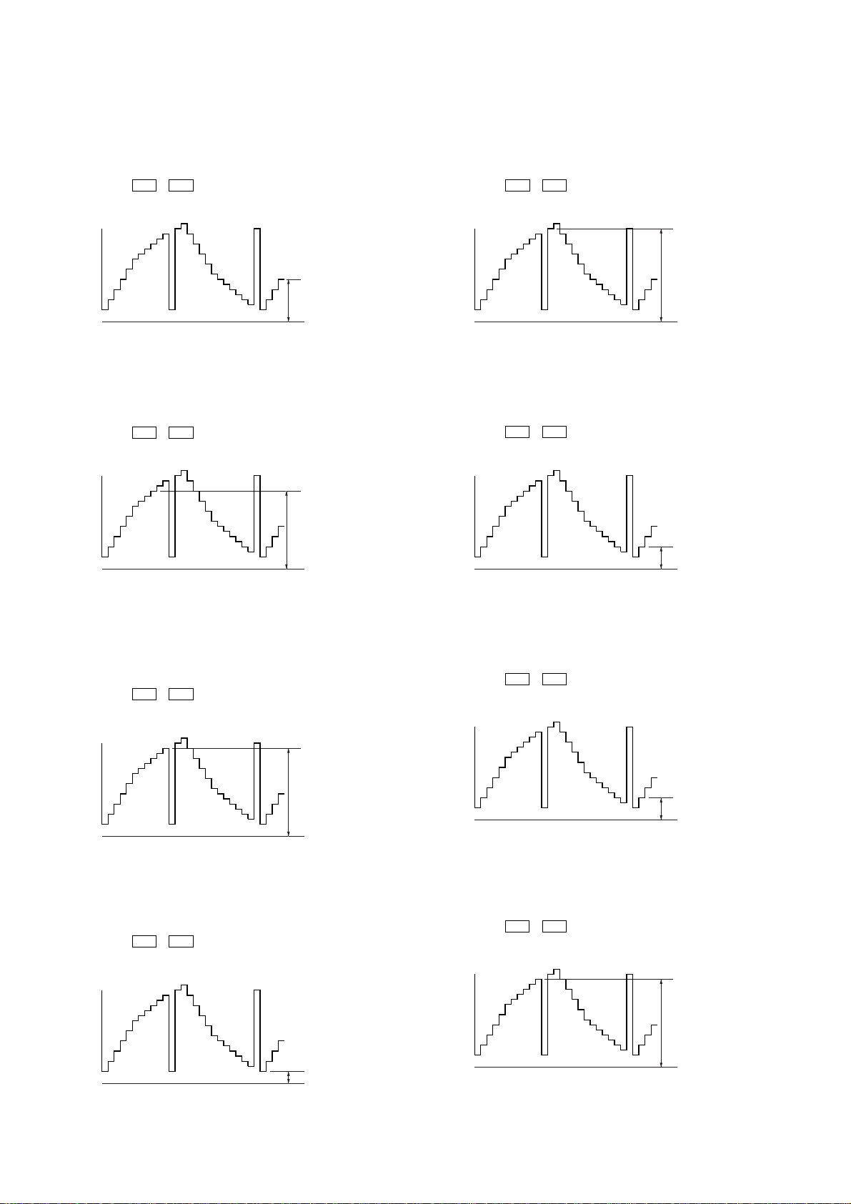
5-7-1. Gamma 1 Adjustment
Adjusting Procedure:
1. Connect an oscilloscope to the TP1964 and TP1901 (GND)
on the MONITOR board.
2. Adjust the
./> keys so that the C level of the
waveform on the oscilloscope is 2.1 ± 0.1 Vp-p.
C
0
5-7-2. Gamma 2 Adjustment
Adjusting Procedure:
1. Connect an oscilloscope to the TP1964 and TP1901 (GND)
on the MONITOR board.
2. Adjust the ./> keys so that the D level of the
waveform on the oscilloscope is 3.0 ± 0.1 Vp-p.
5-7-5. White Limit (White Limiter Level) Adjustment
Adjusting Procedure:
1. Connect an oscilloscope to the TP1964 and TP1901 (GND)
on the MONITOR board.
2. Adjust the ./> ke ys so that the F level of the
waveform on the oscilloscope is 4.0 ± 0.05 Vp-p.
F
0
5-7-6. R-Sub BRT (R-ch Sub Bright) Adjustment
Adjusting Procedure:
1. Connect an oscilloscope of 1 step voltage to the TP1963 and
TP1901 (GND) on the MONITOR board.
2. Adjust the ./> ke ys so that the B level of the
waveform on the oscilloscope is 1.0 ± 0.1 Vp-p.
D
0
5-7-3. Y Gain (Luminance Signal Contrast Level)
Adjustment
Adjusting Procedure:
1. Connect an oscilloscope to the TP1964 and TP1901 (GND)
on the MONITOR board.
2. Adjust the
./> keys so that the E level of the
waveform on the oscilloscope is 3.25 ± 0.1 Vp-p.
E
0
5-7-4. Black Limit (Black Limiter Level) Adjustment
Adjusting Procedure:
1. Connect an oscilloscope to the TP1964 and TP1901 (GND)
on the MONITOR board.
2. Adjust the ./> keys so that the A level of the
waveform on the oscilloscope is 1.0 ± 0.05 Vp-p.
B
0
5-7-7. B-Sub BRT (B-ch Sub Bright) Adjustment
Adjusting Procedure:
1. Connect an oscilloscope of 1 step voltage to the TP1965 and
TP1901 (GND) on the MONITOR board.
2. Adjust the
./> keys so that the B level of the
waveform on the oscilloscope is 1.0 ± 0.1 Vp-p.
B
0
5-7-8. R-Sub CONT (R-ch Sub Contrast) Adjustment
Adjusting Procedure:
1. Connect an oscilloscope of 10 step voltage to the TP1963 and
TP1901 (GND) on the MONITOR board.
2. Adjust the ./> ke ys so that the E level of the
waveform on the oscilloscope is 3.25 ± 0.1 Vp-p.
20
E
A
0
0
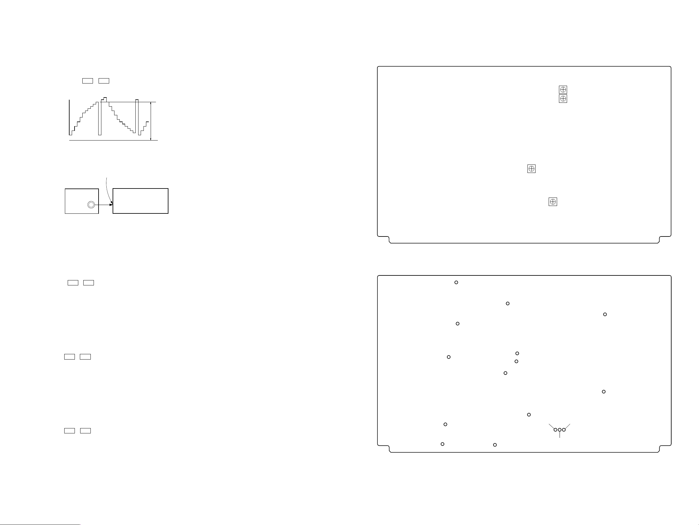
RV1501
V COM Adjustment
RV1901
5.0V Adjustment
RV1902
DC/DC Converter
Frequency Adjustment
RV1651
PLL Adjustment
– MONITOR BOARD (Component Side) –
TP1952
TP1951
TP1954
TP1960
TP1965
TP1964
TP1963
TP1510
TP1909
TP1907
TP1651
TP1901
(GND)
TP1906
TP1515
TP1412
– MONITOR BOARD (Conductor Side) –
TP1421
Adjusting Procedure:
V
NTSC pattern
generator
set
INPUT VIDEO jack
(JK501)
1. Connect an oscilloscope of 10 step voltage to the TP1965 and
TP1901 (GND) on the MONITOR board.
2. Adjust the ./> keys so that the E level of the
waveform on the oscilloscope is 3.25 ± 0.1 Vp-p.
E
0
Connection: (5-7-10 to 5-7-12)
ICF-DVD57TV
Adjustment and Connecting Location:5-7-9. B-Sub CONT (B-ch Sub Contrast) Adjustment
5-7-10. VCO Free Run Adjustment
Condition:
Input the NTSC video signal (10 step (no burst)) (1 Vp-p 75 W) to
the INPUT VIDEO jack (JK501) on the MAIN board from NTSC
pattern generator.
Adjusting Procedure:
Adjust the
./> keys so that a screen on the monitor may
become normal.
5-7-11. PLL/V POS Adjustment
Condition:
Input the NTSC video signal (monoscope) (1 Vp-p 75 W) to the
INPUT VIDEO jack (JK501) on the MAIN board from NTSC
pattern generator.
Adjusting Procedure:
Press the ./> keys to adjust so that the position of screen
on the monitor becomes vertically symmetric.
5-7-12. H POS Adjustment
Condition:
Input the NTSC video signal (monoscope) (1 Vp-p 75 W) to the
INPUT VIDEO jack (JK501) on the MAIN board from NTSC
pattern generator.
Adjusting Procedure:
Press the ./> keys to adjust so that the position of screen
on the monitor becomes horizontally symmetric.
ICF-DVD57TV
2121
ICF-DVD57TV
SECTION 6
DIAGRAMS
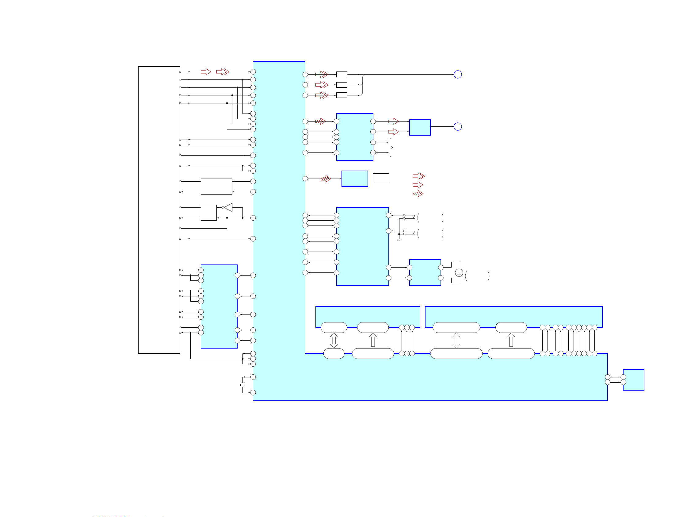
6-1. BLOCK DIAGRAM – DVD Section –
OPTICAL PICK-UP
BLOCK
(KHM-310BAA)
DVDVR
RF
C
B
A
D
PD
MSW
FOCUS/TRACKING COIL DRIVE,
SPINDLE/SLED MOTOR DRIVE
FCS+
FCS– VOFS–13
AUTOMATIC
POWER CONTROL
Q701
Q703
DVD/CD
SWITCH
Q702
IC705
VOFS+14
VNFFC7
6
DVDRF IP
8
MA
9
MB
MC
10
11
MD
DVDA2
DVDB3
DVDC4
DVDD5
TNI18E
TPI19F
V2029VC
MDI120
MDI221
LDO222DVDLD
LDO123CDLD
DVD/CD
114CDVR
LIMIT
136LIMIT SWITCH
1VINFC
FOO42
YUV4/R
200
YUV5/G L.P.F.202
YUV6/B L.P.F.203
ASDATA0 217 AOUTL+ 12
1ACLK 215
2ABCK 214
4ALRCK 213
5ARST 222
SPDIF 225
SO 178 DVD SO054
SI 170
SCK 179 DVD SCK55
XIFCS 169 DVD XIFCS56
XIFBUSY 168 DVD XIFBUSY50
AMUTE 220 DVD AMUT IN57
XPRST 110 DVD RST58
TMS 49 TRAY DET61
Y
L.P.F.
B-Y
R-Y
D/A CONVERTER
IC704
SDTI3
AOUTL– 11
MCLK
BICK
LRCK
AOUTR+ 10
PDN
AOUTR– 9
OPTICAL
TRANSCEIVER
JK502
MAIN SYSTEM CONTROLLER
IC401 (1/3)
DVD SI053
DVD OPEN
DVD CLOSE 42
LOADING A
LOADING B 60
OPTICAL
OUTPUT
R-CH
MIX AMP
IC303
Y, B-Y, R-Y
DVD LCH
A
B
(Page 25)
(Page 24)
• R-ch is omitted due to same as L-ch.
• SIGNAL PATH
: DVD/CD PLAY (VIDEO)
: DVD/CD PLAY (ANALOG AUDIO OUT)
: DVD/CD PLAY (DIGITAL AUDIO OUT)
CLOSE DETECT
MOTOR DRIVE
3
A IN
2
B IN
S001-1
DISC TRAY
OPEN DETECT
S001-2
DISC TRAY
IC351
A OUT
B OUT
8
7
M
M301
DISC TRAY
OPEN/CLOSE
39
DISC TRAY OPEN/CLOSE
51
TRK+ VOTK–16
TRK– VOTK+15
SLED MOTOR+ VOLD–17
SLED MOTOR– VOLD+18
SPINDLE MOTOR+ VOLD–11
SPINDLE MOTOR– VOLD+12
34
36
229
TRO41
FMO38
DMO37
STBY50
OP_OUT
OP_INP
OP_INN35
XTALO228
XTALI
D0 – D7
29, 31, 33, 35,
38, 40, 42, 44
81 – 84,
86 – 88, 91
AD0 – AD7
FLASH ROM
IC707
A-1, A0 – A19
45, 25 – 18, 8 – 1,
48, 17, 16, 9
93, 78, 53 – 59, 75, 74,
72 – 67, 92, 60, 61, 76
IOA0 – IOA20
26
28
11
77
79
66
XIOOE OE
XIOCS CE
XIOWR WE
RF AMP, SERVO DSP,
MPEG DECODER
IC706
DQ0 – DQ15
2, 4, 5, 7, 8, 10, 11, 13, 42,
44, 45, 47, 48, 50, 51, 53
125 – 123, 121, 120, 118, 117,
115, 135, 133 – 128, 126
RD0 – RD15
SD-RAM
IC708
A0 – A11
23 – 26,
29 – 34, 22, 35
147, 149 – 151, 166 – 164,
162, 160, 159, 146, 158
RA0 – RA11
20
143
BA0 BA0/A13
21
145
BA1 BA1/A12
38
37
15
39
18
17
19
16
156
157
113
137
140
139
142
138
5
6EEP_CK 102
EEPROM
IC709
SDA
SCL
RCLK CLK
CKE CKE
DQM0 DQML
DQM1 DQMH
XRAS RAS
XCAS CAS
XRCS CS
EEP_DA 103
XRWE WE
X701
27MHz
26VINTK
23VINLD
6VOSL
28STBY
VNFTK20
ICF-DVD57TV
2222
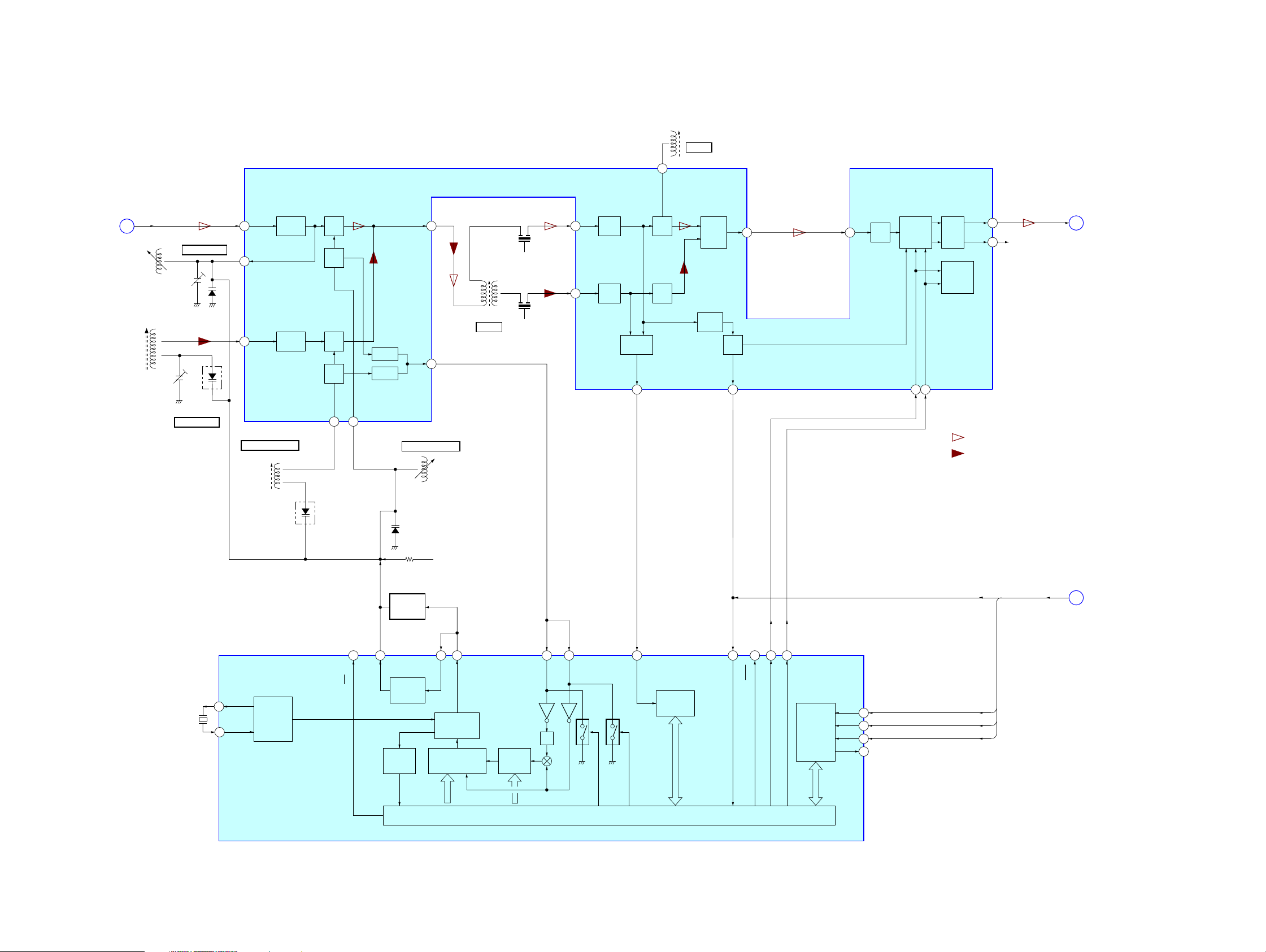
6-2. BLOCK DIAGRAM – TUNER Section –
T2
FM IFT
ICF-DVD57TV
T2
FM IF
(Page 26)
ANT
C
L1
FM RF
L3
AM FERRITE-ROD
ANTENNA
CT3
AM TRACKING
CT1, L1
FM TRACKING
CT1
D3
(1/2)
CT3, L3
FM/AM RF AMP, MIX, OSC,
2
24
D1
22
AM VCO VOLTAGE
L4
AM OSC
FM/AM IF AMP, DET, MPX
IC1
FM
RF IN
FM
RF AMP
FM
RF OUT
AM
RF IN
AM
RF AMP
L4
FM
MIX
FM
OSC
AM
MIX
AM
OSC
AM OSC
20 21
FM OSC
BUFFER
BUFFER
MIX OUT
OSC
OUT
19
L2
FM VCO VOLTAGE
4
FM OSC
10
QUAD
T1
AM IFT
T1
AM IF
CF2
CF4
FM
IF IN
FM IF
7
AMP
AM
IF IN
AM IF
6
AMP
FM
DET
AM
DET
IF
BUFFER
IF OUT
17 18
AF
BUFFER
LEVEL
DET
DET
OUT
ST
IND
ST IND
16
MPX
IN
AF
15
AMP
MPX
LPF1/BAND
LPF2/MO-ST
13
14
MUTE
STEREO/
MONO,
FM/AM
L-OUT
R-OUT
R-CH
TU LCH
D
(Page 24)
12
11
• R-ch is omitted due to same as L-ch.
• SIGNAL PATH
: FM
: AM
L2
X1
75kHz
20
19
FM/AM PLL
IC2
XOUT
XIN
(2/2)
REFERENCE
DIVIDER
D3
D2
VT B+
PLL DATA, PLL CLK,
PLL CE, MUTE
E
(Page 24)
6
FM/AM
LP-OUT
UNLOCK
DETECT
LOW-PASS
FILTER
LOW-PASS
FILTER
PD
LP-IN
PHASE
DETECTOR/
CHARGE PUMP
12 BIT
PROGRAMMABLE
DIVIDER
SWALLOW
COUNTER
111218
FMIN
AMIN
1/2
SHIFT REGISTER & LATCH
10 9
IF IN
UNIVERSAL
COUNTER
ST-IND
BAND
7
BAND
13817 16
MO/ST
CCB
INTERFACE
MUTE
DI
2
CL
3
CE
1
DO
4
PLL DATA
PLL CLK
PLL CE
ICF-DVD57TV
2323
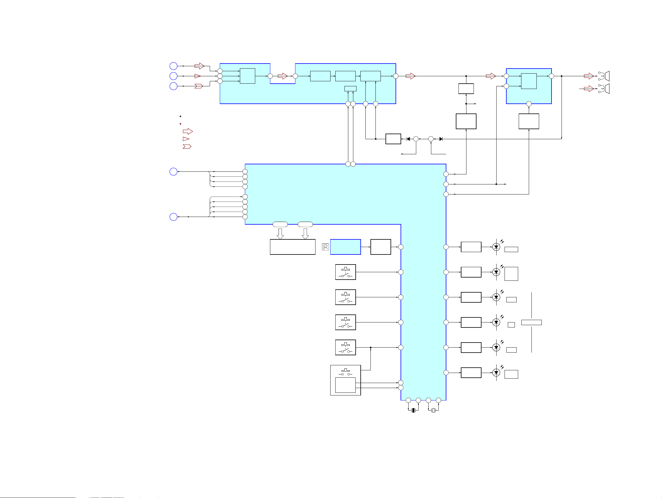
ICF-DVD57TV
6-3. BLOCK DIAGRAM – AUDIO/PANEL Section –
(Page 22)
(Page 23)
(Page 25)
(Page 23)
(Page 25)
DVD LCH
B
TU LCH
D
TV LCH
F
CD LIN
5
R LIN
7 4
TV LIN
9
R-CH : R-ch is omitted due to same as L-ch.
SIGNAL PATH
: DVD/CD PLAY (ANALOG AUDIO OUT)
: FM
: TV (AUDIO)
PLL DATA, PLL CLK,
PLL CE, MUTE
E
µ-COM R DATA,
µ-COM S DATA,
µ-COM CLK,
µ-COM LATCH,
RESET
G
PLL DATA
PLL CLK
PLL CE
MUTE
µ-COM R DATA
µ-COM S DATA
µ-COM CLK
µ-COM LATCH
RESET
INPUT
SELECT
SWITCH
SURROUND/TONE CONTROL
65 RADIO DATA
66 RADIO CLK
64 RADIO CE
63 RADIO MUTE
29 µ-COM R DATA
33 µ-COM S DATA
34 µ-COM CLOCK
37 µ-COM LATCH
36 XRESET
1
INPUT SELECT SWITCH,
ELECTRICAL VOLUME,
IC302
SEG0 – SEG15
10 – 25
COM0 – COM3
V LINSEL L
6 – 9
VOLUME
CONTROL
MAIN SYSTEM CONTROLLER
SURROUND
CONTROL
LOGIC
14SI13SC19
68
IC401 (2/3)
67
VOL CLK
VOL DAT
TONE
CONTROL
BNFL18BOUTL
POWER AMP
IC301
L OUT L IN L OUT
AGC
Q104
17
R-CH
D103
+ +
D102
A MUTE
BUZZER
STBY
78
52
79
R-CH
MUTING
Q103
MUTING
CONTROL
Q302
R-CH
12 3
13
R-CH
NF L
POWER
AMP
STBY
8
STANDBY
SWITCH
Q301
R-CH
SP101
(L-CH)
SP201
(R-CH)
LIQUID CRYSTAL DISPLAY
LCD601
REMOTE CONTROL
RECEIVER
IC601
S659 – 664
S665 – 670
S653 – 658
S652
S651
ROTARY
ENCODER
SIRCS
BUFFER
Q401
48 RC
46 KEY0
45 KEY1
44 KEY2
43 KEY3
40 ENCODE+
41 ENCODE–
X275X1
TIMER LED
OPEN/CLOSE LED
AUX LED
TV LED
DVD LED
TUNER LED
XT271XT1
74
70
80
30
31
32
59
35
LED DRIVE
Q601
LED DRIVE
Q651
LED DRIVE
Q652
LED DRIVE
Q653
LED DRIVE
Q654
LED DRIVE
Q655
D604
TIMER
D651
OPEN/
CLOSE
Z
D652
AUX
D653
TV
D654
DVD
D655
RADIO
BAND
MONITOR ON
ICF-DVD57TV
X401
4.19MHz
X402
32.768kHz
2424
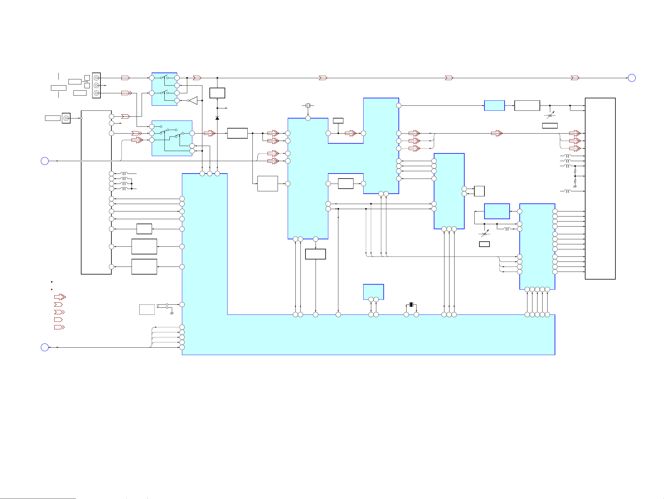
6-4. BLOCK DIAGRAM – MONITOR Section –
TV/AUX AUDIO
SELECT SWITCH
IC502
L
AUDIO
VHF/UHF
A
JK501
INPUT
Y, B-Y, R-Y
VIDEO
TV ANT
R
TU501
TV TUNER UNIT
(Page 22)
R-CH : R-ch is omitted due to same as L-ch.
SIGNAL PATH
: DVD/CD PLAY (ANALOG AUDIO OUT)
: TV (AUDIO)
: TV (VIDEO)
: AUX IN (AUDIO)
: AUX IN (VIDEO)
µ-COM R DATA, µ-COM S DATA,
µ-COM CLK, µ-COM LATCH, RESET
G
(Page 24)
R-CH
25L OUT
R-CH
24R OUT
16DET OUT
Y
239V (MPX)
25V (TU)
145V (F)
265V (D/D)
4SDA
3SCL
15AFT OUT
22MUTE
13RF AGC
20MODE
21F MONO 79 T-FMONO
SELECT SWITCH
SELECT SWITCH
1
4
VIDEO INPUT SELECT SWITCH
3
1
5
TV +9V
TV +5V
AGC
Q501
AUDIO MODE
Q503
AUDIO MODE
Q502
S401
DISPLAY
RELEASE
µ-COM R DATA
µ-COM S DATA
µ-COM CLK
µ-COM LATCH
RESET
2
13
3
5
IC501
Q504
7
4
2
77
32 T-SDATA
33 T-SCL
46 T-AFT
31 T-MUTE
30 T-AGC
78 T-MODE
37 TFT OPEN
57 µCOM-S DATA
56 µCOM-R DATA
58 µCOM-CLK
51 µCOM-LATCH
76 XRESET
80
TV/AUX
MUTING
Q101
34
DVD ON
TV/AUX_MUTE
R-CH
D101, 105
VIDEO AMP
Q505
B-Y
R-Y
SYNC
SEPARATOR
Q1501, 1502
X1501
3.579545MHz
63
VXO-NTSC
52 54 26
57 CIN
5 B-YIN
4 R-YIN
46 34
CTRAPOUT
YIN
CSYNCOUT
CSYNCIN
SDATA
SCLK47HSYNCLOCK
48
SYNC DET
Q1503, 1505
66
67 65
SCL
SDA
HDOUT
VDOUT
39
53
32
31
HSYNCLOCK
TRAP
RGB DECODER
IC1501
BUFFER
Q1504
52
VSYNC
CTRAPIN
VDIN35
HDOUT
VDOUT
EEPROM
IC1451
5
49
VCOMOUT
R-OUT
G-OUT 21
B-OUT 19
R-IN2
G-IN2
B-IN2
POL
BLAK
36
18
POL
BLAK
SDA
SCL
6
50
EEPROM-SCL
EEPROM-SDA
YS 17
SUB SYSTEM CONTROLLER
OSC
RV1651
PLL
V COM AMP
IC1503
PHASE
COMPARATOR
IC1651
HD
VD
BLAK
POL
28
R-OUT
G-OUT
B-OUT
14
15
16
X1401
4.19MHz
74 64
75
X1
X2
IC1401 (1/2)
16
VR
VG
17
18
VB
BLK
15
HSYNCN20
VSYNCN19
OSD DRIVER
IC1502
OSC OUT
OSC IN 8
DATA
SCLK1CSN
3
2
54 55 53
OSD-CLK
OSD-DATA
7
OSD-CS
V COM BIAS
Q1506 – 1510
LCD CONTROLLER
IC1601
33
PD
36
VCO1
37
VCO0
2
HSYNCIN
5
VDBIN
BLACK
8
14
POL
ZOOMZOOM
12
31
61 62 63
JUST4SIDE1
3
JUST
SIDE1
RV1501
V COM
VGH17V
STV1
STV2
STH1
STH2
CPH1
CPH2
CPH3
CPV
OEV1
OEV2
OEV3
OEH
SIDE2
39
35
SIDE2
VEE5V
20
26
23
24
29
27
25
16
19
18
17
RESET
XRESET
ICF-DVD57TV
TV LCH
F
LIQUID CRYSTAL
DISPLAY MODULE
LCD1 (1/2)
VCOM
VCOM
R
G
B
RED
GREEN
BLUE
VGON (17V)
VDD (3.3V)VDD3V
VEE (5.0V)
VB (2.5V)
VSS (–13.0V)VSS–13V
STV1
STV2
STH1
STH2
CLK1
CLK2
CLK3
CPV
OEV1
OEV2
OEV3
OEH21
(Page 24)
ICF-DVD57TV
2525
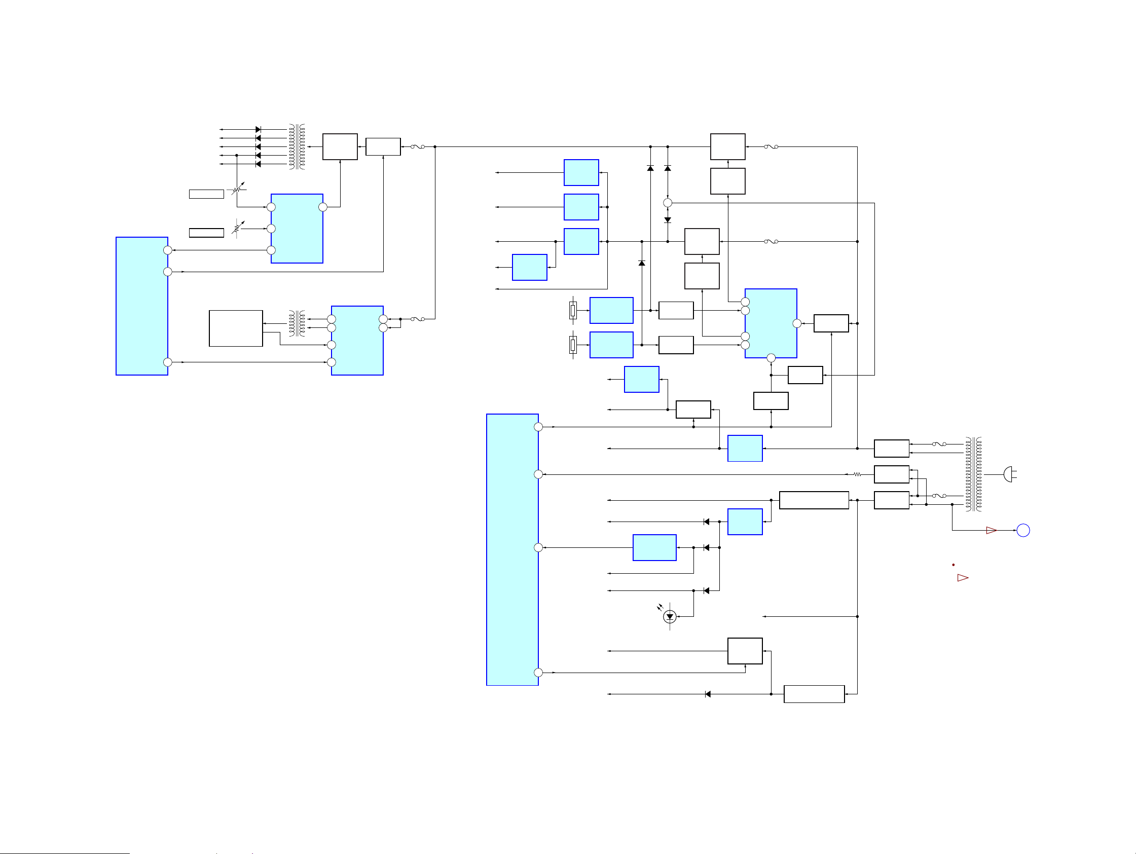
ICF-DVD57TV
6-5. BLOCK DIAGRAM – POWER SUPPLY Section –
D1905
D1904
D1903
D1902
D1901
SUB SYSTEM CONTROLLER
IC1401 (2/2)
41SPC-DET
598V_SW
60TFT-ON
VSS–13V
VGH+17V
VCC+7.5V
VEE+5V
VDD+3.3V
RV1901
5V VOLTAGE
RV1902
FREQUENCY
DISPLAY MODULE
LIQUID CRYSTAL
LCD1 (2/2)
(BACK LIGHT)
DC/DC
CONVERTER
T1901
POWER CONTROL
IC1901
3 7NON1 OUT1
2RT
15 SCP
INVERTER
TRANSFORMER
T1801
DC/DC
CONVERTER
Q1901, 1903
LCD BACK LIGHT
CONTROL
IC1801
8 7OUTL BATT
13 OUTR
2IL
5EN
B+ SWITCH
Q1902, 1904
14BATT
F1801
PLL/RF +3.3V
VIDEO DAC +3.3V
DVD +3.3V
DVD +1.8V
TV +5V
MAIN SYSTEM CONTROLLER
+1.8V
REGULATOR
IC701
IC401 (3/3)
MONITOR ON
AC IN
XRESET
TH902
TH901
62
49
76
+3.3V
REGULATOR
IC702
+3.3V
REGULATOR
IC703
+3.3V
REGULATOR
IC903
TEMPERATURE
TEMPERATURE
DVD +5V
TV +9V
+9V
+5V
SUB µ-COM +3.3V
MAIN µ-COM +3.3V
LED +3.3V
D914, 915 D911
D924, 925
DETECT
IC952
DETECT
IC951
+5V
REGULATOR
IC901
RESET SIGNAL
GENERATOR
IC402
+
D913
DEAD TIME
Q910
DEAD TIME
Q917
B+ SWITCH
Q901, 904
SWITCHING
REGULATOR
Q916
REGULATOR
CONTROL
Q913, 918
D1402
D402
D401
SWITCHING
REGULATOR
Q908
REGULATOR
CONTROL
Q907, 909
REGULATOR
REGULATOR
POWER CONTROL
10 OUT2
11 DT2
7 OUT1
6 DT1
SWITCHING
+9V
IC902
+3.9V
IC904
F903F1901
F904
IC905
9
VCC
SCP
15
SWITCHING
Q902
+5V REGULATOR
Q911, 914, 919, 923, 924
Q903
B+ SWITCH
Q905, 906
RECT
D901
RECT
D905, 906
RECT
D902
F901
F902
T901
POWER
TRANSFORMER
SIGNAL PATH
: FM
ANT
(AC IN)
C
(Page 23)
ICF-DVD57TV
RADIO ON
D651 – 653
(LCD BACK LIGHT)
+6V
RADIO/VT
B+
77
+5.4V
MOTOR DRIVER
B+
D351
+12V
POWER AMP
B+
RADIO ON
SWITCH
Q402
+6V REGULATOR
Q912, 915, 920 – 922
2626
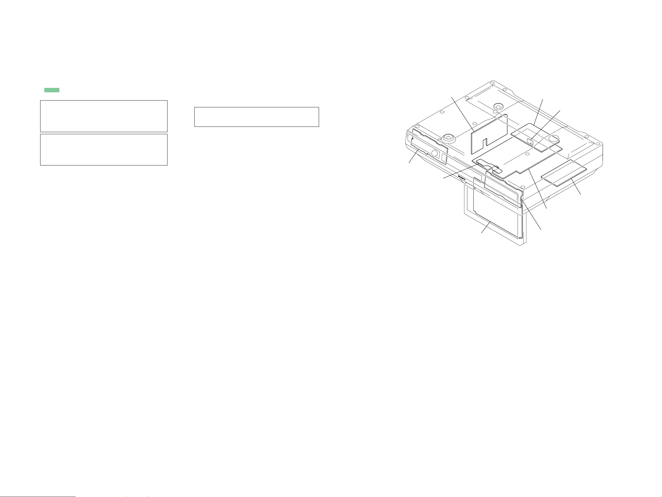
ICF-DVD57TV
• Note For Printed Wiring Boards and Schematic Diagrams
Note on Printed Wiring Board:
• X : parts extracted from the component side.
• Y : parts extracted from the conductor side.
• W : indicates side identified with part number.
• z : Through hole.
• f : inter nal component.
• : Pattern from the side which enables seeing.
(The other layers' patterns are not indicated.)
Caution:
Pattern face side: Parts on the pattern face side seen from
(Conductor Side) the pattern face are indicated.
Parts face side: Parts on the parts face side seen from
(Component Side) the parts face are indicated.
Caution:
Pattern face side: Parts on the pattern face side seen from
(Side B) the pattern face are indicated.
Parts face side: Parts on the parts face side seen from
(Side A) the parts face are indicated.
• DVD board is multi-layer printed board.
However, the patterns of intermediate-layer have not been included in this diagrams.
Note on Schematic Diagram:
• All capacitors are in µF unless otherwise noted. (p: pF)
50 WV or less are not indicated except for electrolytics
and tantalums.
• All resistors are in Ω and 1/
specified.
• f : internal component.
• 2 : nonflammable resistor.
• C : panel designation.
Note: The components identified by mark 0 or dotted line
with mark 0 are critical for safety.
Replace only with part number specified.
• A : B+ Line.
• B : B– Line.
• H : adjustment for repair.
• Voltages and waveforms are dc with respect to ground
under no-signal (detuned) conditions.
– DVD/MONITOR Boards –
no mark : DVD PLAY
(): CD PLAY
[]: TV
〈〈 〉〉 : AUX
∗ : Impossible to measure
– TU Board –
no mark : FM
(): AM
– Other Boards –
no mark : RADIO (FM/AM)
(): DVD PLAY
[]: TV
〈〈 〉〉 : AUX
• Voltages are taken with a V OM (Input impedance 10 MΩ).
Voltage variations may be noted due to normal production tolerances.
• Waveforms are taken with a oscilloscope.
Voltage variations may be noted due to normal production tolerances.
• Circled numbers refer to waveforms.
• Signal path.
L : DVD/CD PLAY (VIDEO)
F : DVD/CD PLAY (ANALOG AUDIO OUT)
J : DVD/CD PLAY (DIGITAL AUDIO OUT)
N : FM
O : AM
E : TV (AUDIO)
a : TV (VIDEO)
d : AUX (AUDIO)
G : AUX (VIDEO)
4
W or less unless otherwise
• Circuit Boards Location
LCD board
MS-203 board
TRANS board
MONITOR board
DVD board
DETECTION board
TU board
MAIN board
KEY board
ICF-DVD57TV
2727
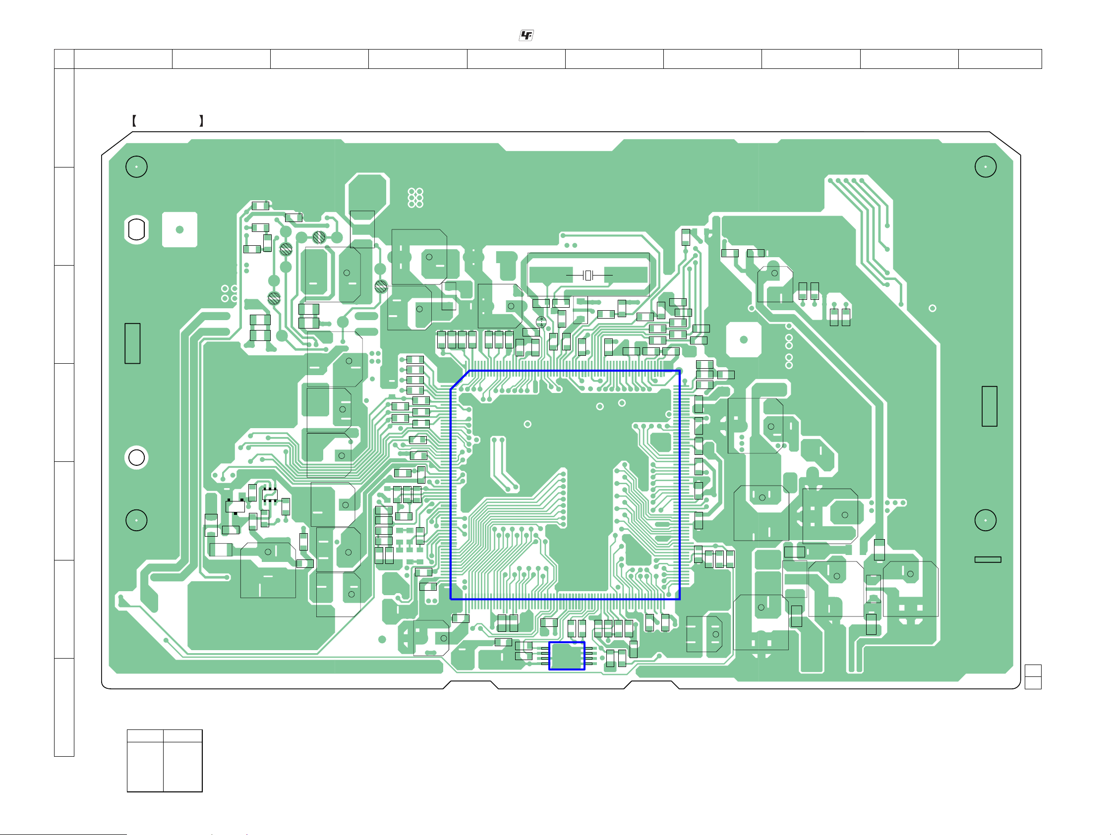
ICF-DVD57TV
6-6. PRINTED WIRING BOARD – DVD Board (Side A) –
1 2 3 4 5 6 7 8 9 10
: Uses unleaded solder.• See page 27 for Circuit Boards Location.
A
B
C
D
E
F
DVD BOARD
(SIDE A)
Q703
BCE
R735
FL706
L704
R734
R739
C741
R725
R727
R742
R731
R821
BP703
2S2G1D
2D1G1S
R736
+
C735
C743
BP704
Q702
R738
R726
R724
C736
BP701
C737
C738
C748
C746
C747
C766
C767
C768
FL707
+
C709
+
BP702
C757
R747
C778
C826
1
64
+
FL709
R787
C779
+
C775
R825
R750
R752
C756
R828
C750
C751
C770
C771
C772
C773
C774
R751
R753
R761
C776
R827
R746
C764
C765
+
+
+
+
R826
R745
R824
R744
+
+
C807
C825
C822
R835
256 193
65 128
C821
C838
+
C818
C780
C808
C813
C781
R793
R792
C804 C803
BP601
C812
IC706
C782
5
IC709
8
R784
R782
C802
R803
X701
FL711
C800
R804
4
1
R781
C783
C799
R764
C787
C801
R813
R779
R777
C798 C797 C796
R805
R766
C784
C870
R765
C869
C785
C847
C728
R780
R778
R713
C727
C726
192
129
R714
R768
R767 R769
C795
C791 C792 C793 C794
C790C789
C788
C861
R806
+
C837
R728
C724
C708
+
C707
+
C701
+
C723
+
FB704
C719
FL702
FB703
C721
C714
C722
+
C702
+
C720
FB706
FL703
FB705
+
C703
1-866-128-
11
(11)
G
ICF-DVD57TV
• Semiconductor
Location
Ref. No. Location
IC706 E-5
IC709 F-6
Q702 E-3
Q703 E-2
2828
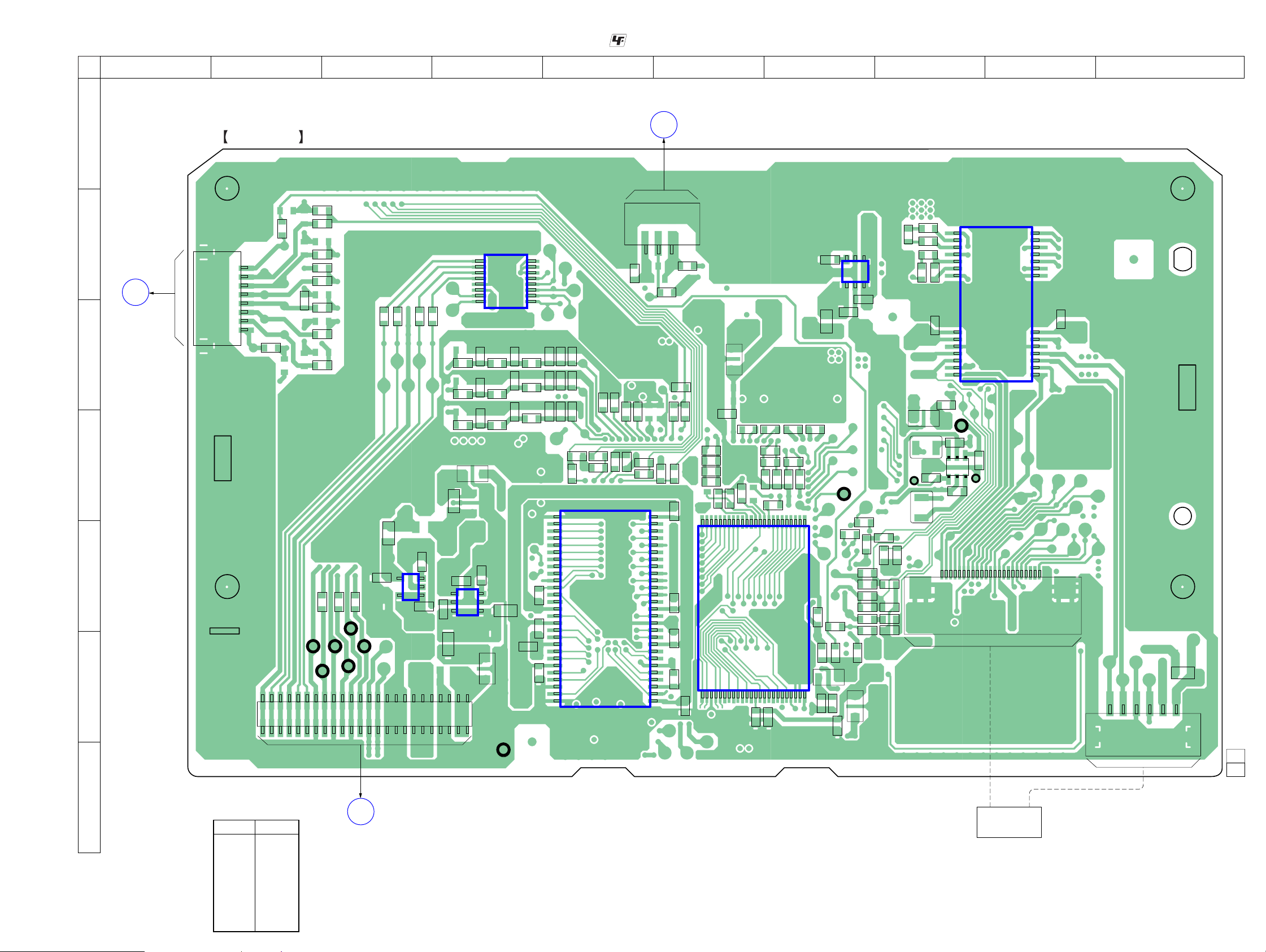
6-7. PRINTED WIRING BOARD – DVD Board (Side B) –
1 2 3 4 5 6 7 8 9 10
A
B
C
MAIN
BOARD
CN454
(Page 34)
C
DVD BOARD
8
CN704
1
R840
R841
(SIDE B)
C841
R801
R800
C843
R799
C849
R798
R797
R796
D
E
TP711
TP709
TP710
F
1
FB712
FB711
TP707
TP708
CN701
FB710
TP706
R712
R706
C715
4
5
IC703
R711
C716
R710
C717
3
1
R709
R717 L701
R720 L702
R718 L703
R701
C706
4
C705
6
IC701
FB702
9
16
FL705
24
IC704
C729
C731
C730
C704
3
1
R794
FL701
FB709
C732
FB708
C734
FB707
C733
C830
8
1
28
C852
C840C839
54
R815
R819
R817
R814
R818
R816
R721
R723
R722
R810C859
R811
IC708
C858
R771
R772
R809
: Uses unleaded solder.• See page 27 for Circuit Boards Location.
R773
C857
R837
R774
C856
R808
B
CN705
R838
C855
27
1
MAIN BOARD
CN355
(Page 34)
13
R839
FL712
C860
R770
R807
C809
R812
C810 C811 C823 C824
R785
R833
R834
C805
R836
R791
24 1
IC707
C832 C833 C834 C835
25 48
C831
R790
C817
C816 C820
C815
C814
R788
C829
C871
IC702
C819
R786
C712
R703
C763
R762
L707
FL710
R763
4
C710
TP761
C758
R760
R832
C827
13
C711
C755
R829
R755
R758
R830
R831
C777
R748
FL713
6
R754
C759
C760
C761
R759
C762
TP751
R743
R823
R822
FL708
L705
C742
R737
R732
R820
R740
L706
R733
C739
14
C749
1
7
8
C744
Q701
C745
TP752
2E1B1C
2C2B1E
IC705
R741
TP753
CN702
ICF-DVD57TV
28
22
C740
21
15
241
R729
16
CN703
G
ICF-DVD57TV
• Semiconductor
Location
Ref. No. Location
IC701 E-4
IC702 B-7
IC703 E-3
IC704 B-4
IC705 C-9
IC707 E-6
IC708 E-5
Q701 D-8
A
MAIN BOARD
CN354
(Page 34)
TP702
11
1-866-128-
OPTICAL PICK-UP
BLOCK
(KHM-310BAA)
(11)
2929
 Loading...