

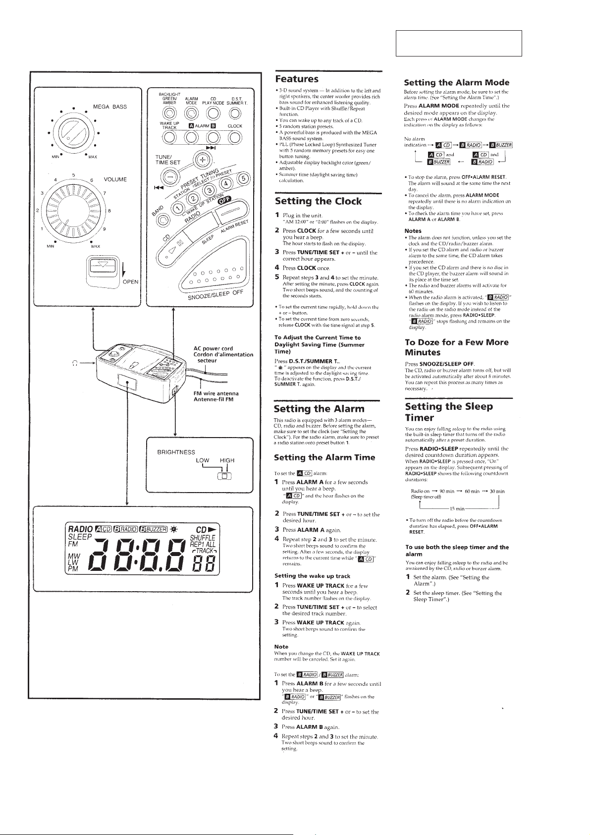
Page 1
ICF-CD873L
SERVICE MANUAL
Ver 1.0 1999. 05
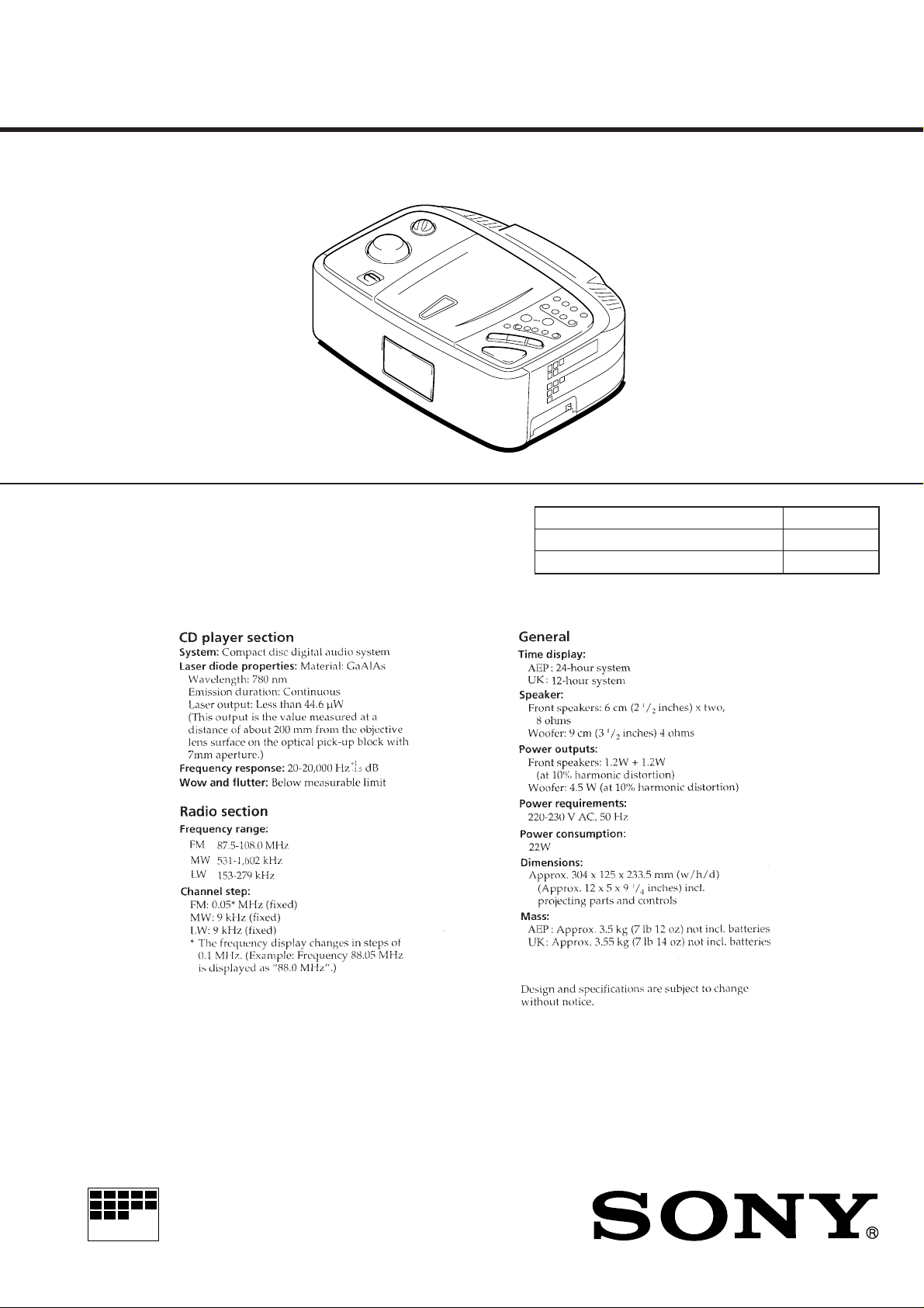
SPECIFICATIONS
AEP Model
UK Model
Model Name Using Similar Mechanism CFD-550
Optical Device Name KSM-213BAN
Optical Pick-UP Name KSS-213B
MICROFILM
Supplied accessories:
Instruction manual (1)
FM/MW/LW CD CLOCK RADIO
Page 2
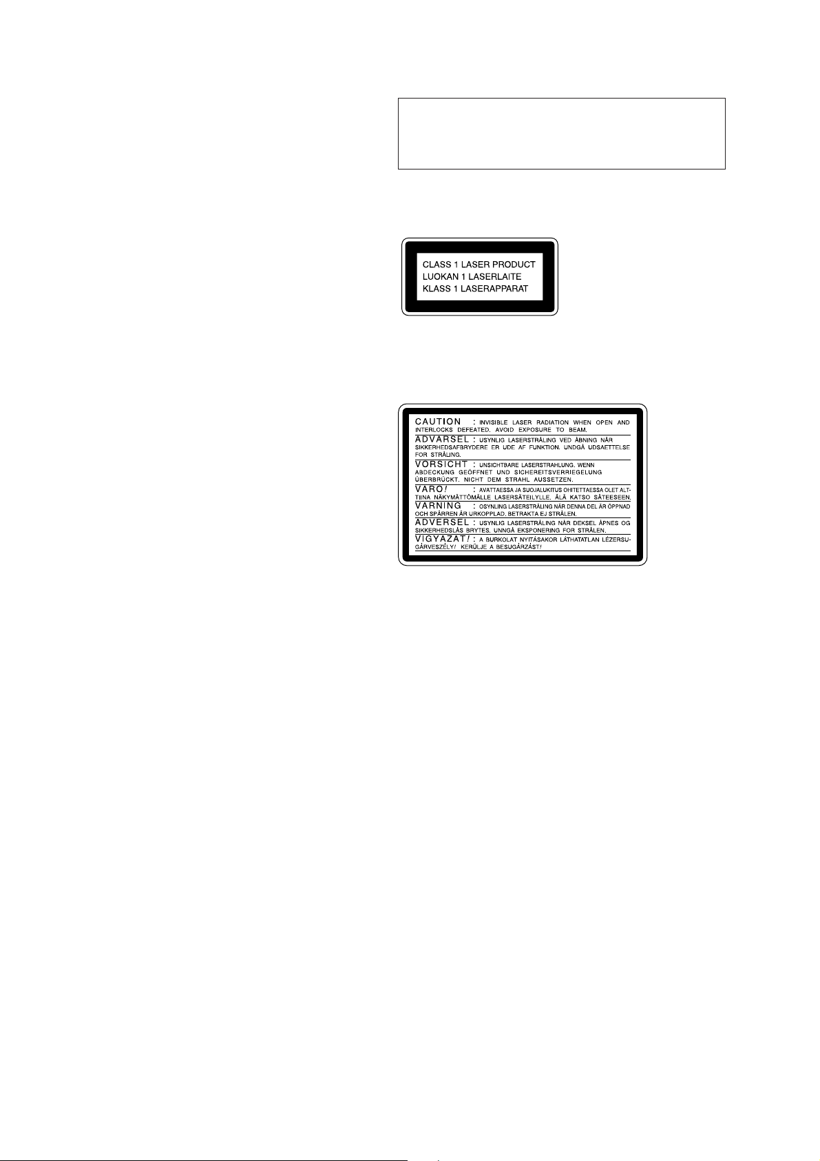
TABLE OF CONTENTS
1. SERVICING NOTES............................................... 3
2. GENERAL ................................................................... 4
CAUTION
Use of controls or adjustments or performance of procedures
other than those specified herein may result in hazardous radiation exposure.
3. DISASSEMBLY ......................................................... 5
4. POWER CORD SETTING................................... 7
5. ELECTRICAL ADJUSTMENTS
Tuner Section .................................................................. 8
CD Section ...................................................................... 9
Main Clock Section......................................................... 11
6. DIAGRAMS
6-1. Block Diagram – CD Section – ..................................... 13
6-2. Block Diagram – TUNER Section – ............................. 15
6-3. Block Diagram – MAIN Section – ................................ 17
6-4. Printed Wiring Boards – MAIN Section – .................... 22
6-5. Schematic Diagram – MAIN Section –......................... 25
6-6. Schematic Diagram – POWER SUPPLY Section –...... 30
6-7. Printed Wiring Boards
– POWER SUPPLY Section – ...................................... 33
6-8. IC Pin Function Description ........................................... 39
7. EXPLODED VIEWS ................................................ 41
8. ELECTRICAL PARTS LIST ............................... 45
This appliance is classified as a CLASS 1 LASER product.
The CLASS 1 LASER PRODUCT MARKING is located on
the rear exterior.
Laser component in this product is capable of emitting radiation
exceeding the limit for Class 1.
The following caution label is located inside the unit.
SAFETY-RELATED COMPONENT WARNING!!
COMPONENTS IDENTIFIED BY MARK ! OR DOTTED
LINE WITH MARK ! ON THE SCHEMATIC DIAGRAMS
AND IN THE PARTS LIST ARE CRITICAL TO SAFE
OPERATION. REPLACE THESE COMPONENTS WITH
SONY PARTS WHOSE PART NUMBERS APPEAR AS
SHOWN IN THIS MANUAL OR IN SUPPLEMENTS PUBLISHED BY SONY.
– 2 –
Page 3
SECTION 1
CF2
CF3
mark
SERVICING NOTES
NOTES ON HANDLING THE OPTICAL PICK-UP
BLOCK OR BASE UNIT
The laser diode in the optical pick-up block may suffer electrostatic break-down because of the potential difference generated
by the charged electrostatic load, etc. on clothing and the human
body.
During repair, pay attention to electrostatic break-down and also
use the procedure in the printed matter which is included in the
repair parts.
The flexible board is easily damaged and should be handled with
care.
NOTES ON LASER DIODE EMISSION CHECK
The laser beam on this model is concentrated so as to be focused
on the disc reflective surface by the objective lens in the optical
pick-up block. Therefore, when checking the laser diode emission, observe from more than 30 cm away from the objecti ve lens.
CHUCK PLATE JIG ON REPAIRING
On repairing CD section, playing a disc without the CD lid, use
Chuck Plate Jig.
• Code number of Chuck Plate Jig: X-4918-255-1
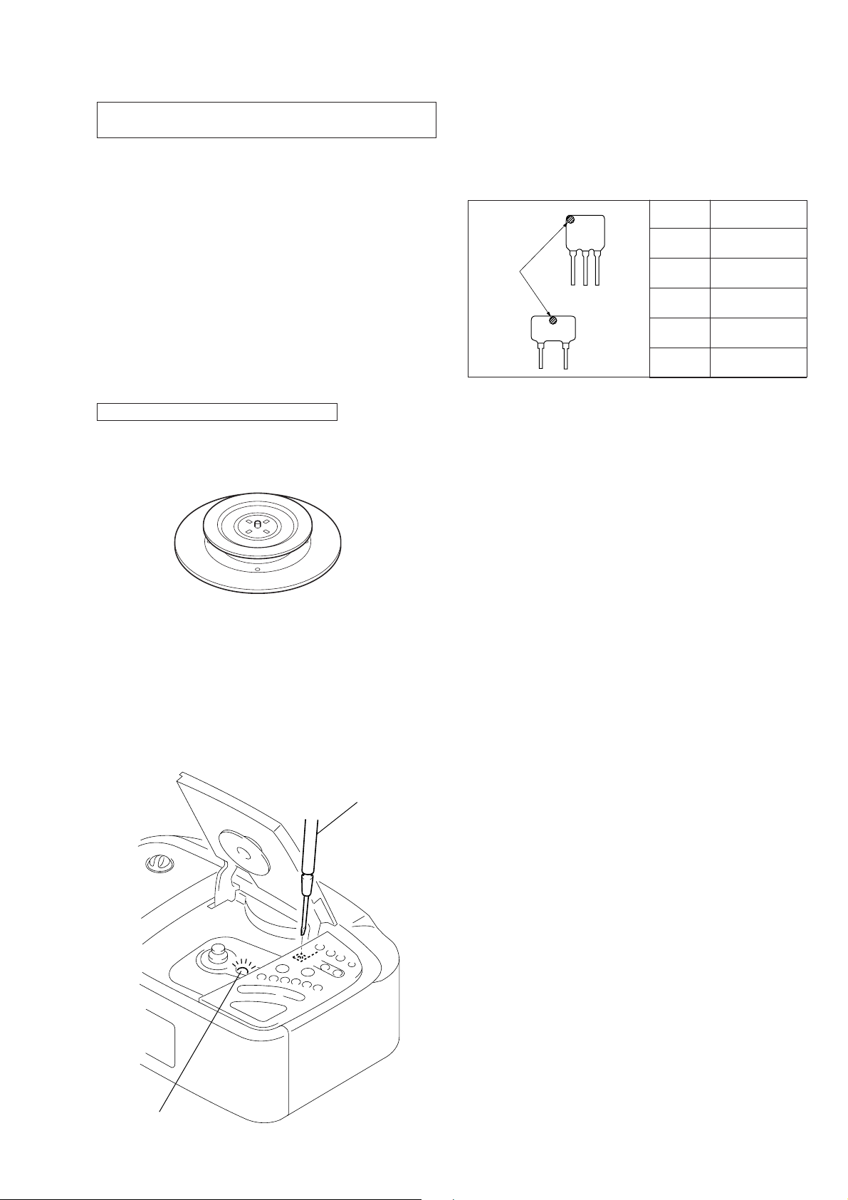
HOW TO CHANGED THE CERAMIC FILTERS
This model is used two ceramic filters of CF2 and CF3.
You must used same type of color marked ceramic filters in order
to meet same specifications.
Therefore, the ceramic filter must changed two pieces together
since it’s supply two pieces in one package as a spare parts.
Mark Center frequency
red 10.70 MHz
blue 10.67 MHz
orange 10.73 MHz
black 10.64 MHz
white 10.76 MHz
Flexible Circuit Board Repairing
• Keep the temperature of the soldering iron around 270 ˚C during repairing.
• Do not touch the soldering iron on the same conductor of the
circuit board (within 3 times).
• Be careful not to apply force on the conductor when soldering
or unsoldering.
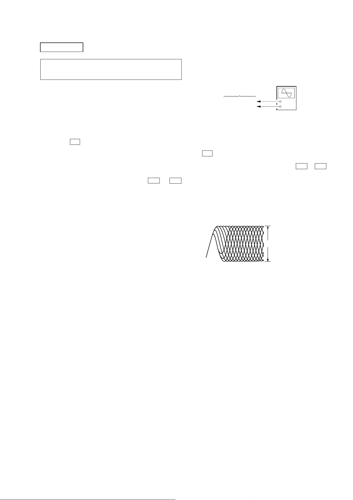
LASER DIODE AND FOCUS SEARCH OPERATION
CHECK
1. Open the CD lid.
2. Turn on S424 as following figure.
3. Conf irm that the laser diode emission while observing the objecting lens. When there is no emission, Auto Power Control
circuit or Optical Pick-up is broken.
Objective lens moves up and down once for the focus search.
Insert a precision
screwdriver and
push S424.
Notes on chip component replacement
• Never reuse a disconnected chip component.
• Notice that the minus side of a tantalum capacitor may be damaged by heat.
laser diode
emission
– 3 –
Page 4
SECTION 2
GENERAL
This section is extracted from
instruction manual.
– 4 –
Page 5
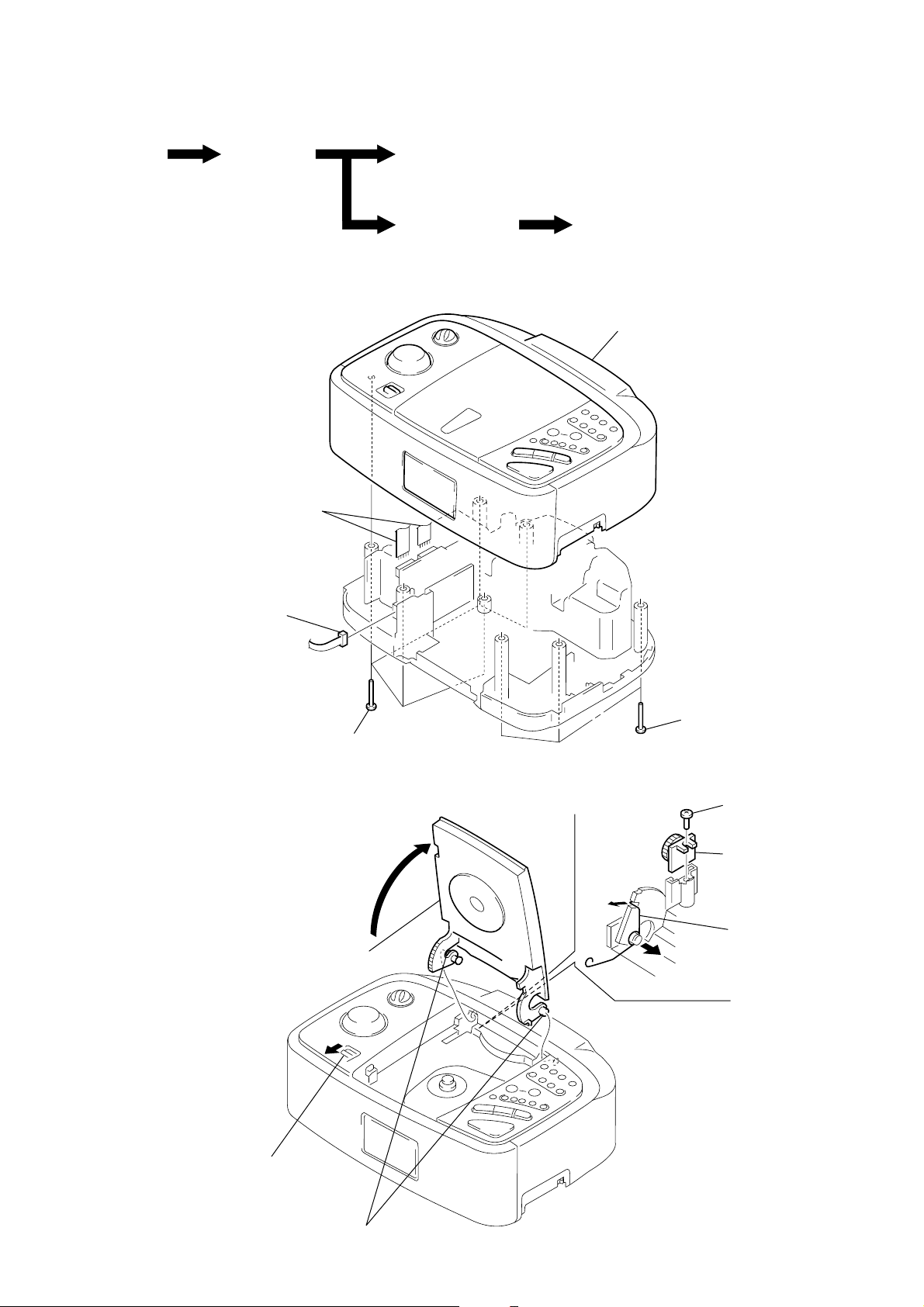
• This set can be disassembled in the order shown below.
SECTION 3
DISASSEMBLY
Set
Note: Follow the disassembly procedure in the numerical order given.
Upper cabinet
section
CD lid assy
Main board section Optical pick-up section
UPPER CABINET SECTION
3
two flat wires
(CN303, 304)
2
upper cabinet section
CD LID ASSY
4
connector
(CN306)
1
five screws
(P3
2
Open the CD lid assy.
7
Remove the CD lid
assy.
×
14)
1
three screws
(P3
×
3
4
14)
5
screw
(B3
damper
×
10)
spring
(CD open)
1
Pull the button (open).
6
two bosses
– 5 –
Page 6
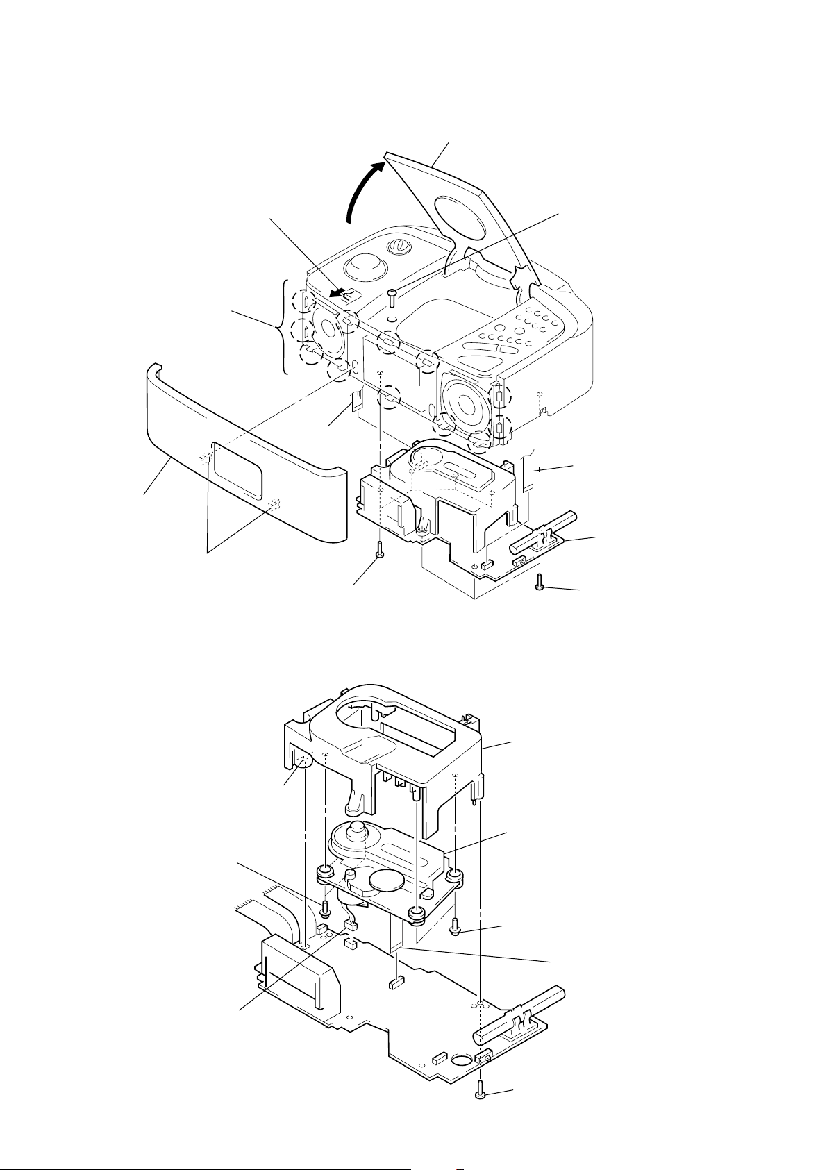
MAIN BOARD SECTION
1
2
net assy
3
Pull the button (open).
twelve
claws
7
flat wire
(CN301)
4
Open the CD lid.
5
screw
(B3
7
×
10)
flat wire
(CN402)
1
two claws
OPTICAL PICK-UP SECTION
6
two screws
(PWH2.6
×
2
10)
claw
6
four screws
(P3
×
14)
3
CD chassis
7
optical pick-up
section
6
two screws
(PWH2.6
×
6
10)
8
main board
section
three screws
(P3
×
14)
5
connector
(CN502)
– 6 –
1
4
screw
(BTP3
flat wire
(CN501)
×
8)
Page 7
SECTION 4
POWER CORD SETTING
Set the power cord as illustrated below, then install the lower cabinet section.
Power Cord
lower cabinet section
– 7 –
Page 8
SECTION 5
)
)
1 µF
TP8 (VCO)
+
–
frequency counter
33 k
Ω
TP7 (+B)
+
MAIN board
ELECTRICAL ADJUSTMENTS
TUNER SECTION 0 dB=1 µV
[MW/LW]
Setting:
Function : RADIO
Band switch: MW or LW
AM RF signal
generator
30% amplitude
modulation by
400 Hz signal
Output level: as low as possible
[FM]
Setting:
Function : RADIO
Band switch: FM
FM RF signal
generator
22.5 kHz frequency
deviation by 400 Hz
signal
Output level: as low as possible
• Repeat the procedures in each adjustment several times, and the
frequency coverage and tracking adjustments should be finally
done by the trimmer capacitors.
• Remove FM antenna in FM adjustments.
Put the lead-wire
antenna close to
the set.
set
MAIN board
TP12 (FM IN)
0.01 µF
set
MAIN board
TP53 (VT)
2
2
digital voltmeter
100 k
Ω
level meter
32
Ω
+
–
(headphone) jack (J301
level meter
32
Ω
+
–
(headphone) jack (J301
AM IF ADJUSTMENT
Adjust for a maximum reading on level meter
T1 450 kHz
MW FREQUENCY COVERAGE ADJUSTMENT
Adjustment Part Frequency Display Reading on Digital Voltmeter
L4 531 kHz 2.8 V
Confirmation 1,602 kHz less than 10.5 V
MW TRACKING ADJUSTMENT
Adjust for a maximum reading on level meter
L3-1 621 kHz
CT2 1,404 kHz
LW FREQUENCY COVERAGE ADJUSTMENT
Adjustment Part Frequency Display Reading on Digital Voltmeter
CT4 153 kHz 2.2 V
Confirmation 279 kHz less than 9.5 V
LW TRACKING ADJUSTMENT
Adjust for a maximum reading on level meter
L3-2 162 kHz
CT3 243 kHz
FM FREQUENCY COVERAGE ADJUSTMENT
Adjustment Part Frequency Display Reading on Digital Voltmeter
L2 87.5 MHz 2.1 V
Confirmation 108 MHz 9.7 V
FM TRACKING ADJUSTMENT
Adjust for a maximum reading on level meter
L1 87.5 MHz
CT1 108 MHz
Adjustment Location: MAIN board (See page 12)
FM VCO Adjustment
Setting:
FM RF SSG
0.01 µF
Carrier frequency: 98 MHz
Modulation: 400 Hz, 30% FM modulation
Output level: 0.1 V (100 dB)
MAIN board
TP12 (FM IN)
set
Procedure:
1. Connect the frequency counter to TP7, 8 as shown the figure
below.
2. Tune the set to 98 MHz.
3. Adjust RV1 for 76 kHz reading on the frequency counter.
Specified Value: 75.95 to 76.05 kHz
Adjustment Location: MAIN board (See page 12)
– 8 –
Page 9
CD SECTION
Note:
Tracking Balance Adjustment and Tracking Gain Adjustment are
done automatically in this set.
TEST MODE
1. Press the CD LID OPEN/CLOSE DET switch (S424) on the
PUSH SWITCH board.
2. Under standby condition (when the clock appears in the display), short the BP (CD TEST AUTO).
Note: If the power is supplied to the microprocessor once, it is backed up
for 3 minutes, therefore the TEST mode will not be activ ated within
3 minutes even if the power is turned on again. In this case, short
instantaneously the BP (CD TEST MANUAL).
3. Press the fl key, and the focus search is repeated.
At this time, check that the optical pick-up objective lens moves
smoothly without a sticking or noise.
4. Load the test disc (YEDS-18: Part No. 3-702-101-01), and perform automatic adjustment after the focus search succeeded.
5. After automatic adjustment is finished, move the sled motor
to the center. At this time, keep pressing the + and =
keys to confirm that optical pick-up mov es smoothly via most
inside track → most outside track → most inside track without a sticking or noise.
6. Confirm the traverse waveform.
7. Press the [WAKEUPTRACK] key.
8. The tracking servo and the sled servo are turned on, the mute
is cancelled.
9. Playback the 2nd track.
10. Adjust the RF and jitter waveforms.
Connecting points: MAIN Board (See page 12)
Focus Bias Adjustment
This adjustment is to be done when the optical block is replaced.
Connection:
oscilloscope
(AC range)
MAIN board
TP503 (RF)
TP504 (VREF)
+
–
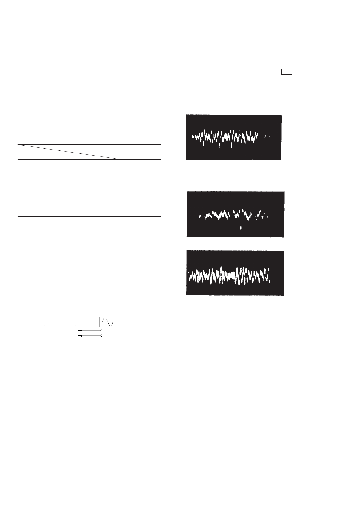
Adjustment Procedure:
1. Connect the oscilloscope to TP504 (VREF) and TP503 (RF)
on the MAIN board.
2. Insert the test disc (YEDS-18: Part No.3-702-101-01) and press
fl key to play.
3. Move the optical pick-up to the music area on the disc to enable easy visibility of the eye pattern by + or = key
pressing.
4. Adjust RV501 so that the oscilloscope waveform is as shown
in the figure below (eye pattern).
A good eye pattern means that the diamond shape (≈) in the
center of the waveform can be clearly distinguished.
• RF signal reference waveform (eye pattern)
VOLT/DIV: 0.2 V
TIME/DIV: 500 ns
±
0.5 Vp-p
1.3
When observing the eye pattern, set the oscilloscope
for AC range and raise vertical sensitivity.
Adjustment Location: MAIN Board (See page 12)
– 9 –
Page 10
Focus Gain Adjustment
A frequency response analyzer is necessary in order to perform
this adjustment exactly.
However, this gain has a margin, so even if it is slightly off, there
is no problem. Therefore, do not perform this adjustment.
Focus gain determines the optical pick-up follow-up (v ertical and
horizontal) relative to mechanical noise and mechanical shock
when the 2-axis device operate.
However , as these reciprocate, the adjustment is at the point where
both are satisfied.
• When gain is raised, the noise when the 2-axis device operates
increases.
• When gain is lowered, mechanical shock and skipping occurs
more easily.
• When gain adjustment is off, the symptoms below appear.
Procedure:
1. Keep the set horizontal.
If the set is not horizontal, this adjustment cannot be per-
(
formed due to the gravity against the 2-axis device
2. Insert the test disc (YEDS-18) and press the fl button.
3. Connect the oscilloscope BT (FEO) and TP504 (VREF) on
the MAIN board.
4. Adjustment RV502 on the MAIN board so that the w a veform
is as shown in the figure below.
VOLT/DIV: 100 mV
TIME/DIV: 2 mS
100 mV
)
Symptoms
• The time until music starts becomes longer for
STOP → PLAY or automatic selection.
(=, + buttons pressed)
(Normally takes about 2 seconds)
• Music does not start and disc continues to
rotate for STOP → PLAY or automatic
selection.
(=, + buttons pressed)
• Sound is interrupted during PLAY.
Or time counter display stops progressing.
• More noise during 2-axis device operation
Gain Focus
low
–
–
high
The following is a simple adjustment method.
– Primary Adjustment –
Note: Since exact adjustment cannot be performed, remember the posi-
tions of the controls before performing the adjustment. If the positions after the primary adjustment are only a little different, return
the controls to the original position.
Connection:
oscilloscope
MAIN board
BP (FEO)
TP504 (VREF)
+
–
0 V
• Incorrect Examples (DC level changes more than on adjusted
waveform)
low focus gain
high focus gain
VOLT/DIV: 100 mV
TIME/DIV: 2 mS
200 mV
0 V
VOLT/DIV: 100 mV
TIME/DIV: 2 mS
75 mV
0 V
Adjustment Location: MAIN Board (See page 12)
– 10 –
Page 11
MAIN CLOCK SECTION
Main Clock Adjustment
Connection:
MAIN board
TP (+5 V)
TP401 (X2)
TP GND (SHIELD)
adjustment
jig
+5
OUT
IN
GND
GND
10 : 1 probe
Adjustment jig:
+5 V
IN
GND
+
0.5 pF
47 uF
1 M
1 M
Ω
Ω
Ω
1000 pF
INVERTER
(TC7W04F)
100 k
Ω
OUT
GND
100 k
Procedure:
1. Connect the frequency counter as the above figures.
2. Adjust CT401 for 4.2495 MHz reading on the frequency
counter.
Specified V alue: 4.2490 to 4.2500 MHz
frequency counter
+
–
– 11 –
Page 12

Adjustment Location and Connecting Points:
t
RV502 Focus Gain Adjustment
RV501 Focus Bias Adjustment
– MAIN BOARD (Component Side) –
L4 MW Frequency Coverage Adjustment
CT4 LW Frequency Coverage Adjustment
FM T rac king Adjustment
LW Tracking Adjustment
CT1
L1
T1 AM IF Adjustment
L3-2
CT3
CT2
MW T rac king Adjustmen
L3-1
RV1 FM VCO Adjustment
L2
FM Frequency Coverage
Adjustment
– MAIN BOARD (Conductor Side) –
TP401
(X2)
TP GND
(SHIELD)
C429
+
BP (CD TEST AUTO)
CT401 Main Clock Adjustment
BP (CD TEST MANUAL)
TP (+5 V)
TP503 (RF)
TP504 (VREF)
TP7
(+B)
TP13 (FM IN GND)
TP12 (FM IN)
TP50 (VT GND)
BP (FEO)
TP53 (VT )
TP8
(VCO)
– 12 –
Page 13

6-1. BLOCK DIAGRAM – CD Section –
ICF-CD873L
SECTION 6
DIAGRAMS
DETECTOR
D
A
C
B
F
E
OPTICAL PICK-UP
(KSS-213B)
LASER DIODE
PD
MAIN BOARD (1/3)
CN501
12
5
13 4
10 7
11 6
98
14 3
107
POWER CONTROL
LD
125
PHD1
35
PHD2
36
AUTOMATIC
Q502
PD1 I-V AMP
PD2 I-V AMP
+
F
38
E
39
LD
33
RF
SUMMING
AMP
RF AMP,
FOCUS/TRACKING
SERVO
IC501 (1/2)
F I-V
AMP
E I-V
AMP
LD
AMPPDAMP
FOCUS
ERROR
AMP
TRACKING
ERROR
AMP
FE BIAS
PHD
34
RFO
31
RFI
30
FOCUS OK
COMPARATOR
MIRR
DEFECT
FEO
1
37
TEO
42
EI
40
AMP
AMP
RV502
FOCUS
GAIN
RV501
FOCUS
BIAS
FOCUS OK
AMP
TTL
IIL
FEI FEO
2
TEI
44
TTL
IIL
IIL
IIL DATA REGISTER
TTL
FOCUS PHASE
COMPENSATION
TRACKING PHASE
COMPENSATION
FOK
DATA
CLK
XLT
XRST
SENS
C.OUT
TAO
25
21
19
20
22
24
23
6
13
DIGITAL SIGNAL PROCESSOR,
CLV SERVO, D/A CONVERTER
IC502
RF
ASYMMETRY
36
CORRECTION
ASYI
38
ASYO
39
XPCK
50
FOK
23
DATO
15
CLKO
17
XLTO
16
8
XRST
SERVO AUTO SEQUENCER
SEIN
13
CNIN
14
DIGITAL
CLV
MDP
MDS26MON24LOCK
25
FILTER
3031
3429
FILI
PCO
FILO
CLTV
DIGITAL PLL
27
D414
DEMODULATOR
SQSO
SQCK
SENS
4 5 7 9 11 1012 3
42CK39
41
SQSI
SENS
ERROR
CORRECTOR
EFM
SUB-CODE
PROCESSOR
CPU INTERFACE
DATA
CLOK
XLAT
30
31
32
DATA
CLOCK
MUTE
45
47
43
6
PCMDI
BCKI
LRCKI
63
CLOCK
GENERATOR
EMPHI
C4M
60
LPWM
70
NLPWM
69
RPWM
78
NRPWM
XTAI
XTAO
XTSL
77
73
74
21
DIGITAL FILTER &
1 BIT D/A CONVERTER
LOW-PASS
FILTER
IC301
X501
16.933MHz
DATA, CLOCK, LATCH
CD L-CH
CD R-CH
A
(Page 17)
B
(Page 16)
16K
RAM
PCMD
44
D/A INTERFACE
OUT
20
CLOCK
BCK
LRCK
C2PO
DOUT
XUGF
WFCK
EMPH
GFS
46
42
54
61
49
64
62
51
INTERNAL BUS
DIGITAL
XLON
EXCK
B+
22 18
SPOA
SPOB19SPOC
SCOR
SBSO
(CD 5V)
44
XLT
SCOR
M570
(SLED)
M571
(SPINDLE)
S570
(LIMIT)
2-AXIS
DEVICE
(FOCUS)
M
M
(TRACKING)
1
3
5
4
6
7
CIN
FOCUS/TRACKING COIL DRIVE,
SPINDLE/SLED MOTOR DRIVE
IC503
143
152
134
161
T-OUT+
27
T-OUT–
26
F-OUT+
18
F-OUT–
17
TRACKING
COIL DRIVE
FOCUS
COIL DRIVE
T-IN
F-IN
25
19
E-F BALANCE
CONTROL
Q501
BP
(CD TEST MANUAL)
43
CD ADJ
29
SYSTEM CONTROLLER
X-RESET
34
IC401 (1/2)
DATA
R-LAT
DOOR-IN
40
37
62
DATA
LATCH
S424
(CD LID OPEN/CLOSE DET)
PUSH SWITCH BOARD
SLED SERVO
CN502BH570
1
2
4
3
5
6
2
1
12
11
SL-OUT+
SL-OUT–
SP-OUT+
SP-OUT–
SLED
MOTOR DRIVE
SPINDLE
MOTOR DRIVE
SL-IN
3
SP-IN
10 1514
IC501 (2/2)
SLO
16 14
SLED
AMP
SLP
SP-OUT
SP-IN
MUTE
7
MOTOR BOARD
05
• SIGNAL PATH
: CD PLAY
– 13 – – 14 –
Page 14

ICF-CD873L
6-2. BLOCK DIAGRAM – TUNER Section –
ANT1
FM WIRE
ANTENNA
MAIN BOARD (2/3)
CT1, L1
FM TRACKING
CT2, L3-1
MW TRACKING
L3
MW/LW FERRITE-ROD
ANTENNA
L3-1
(MW)
L3-2
(LW)
CT3
CT3, L3-2
LW TRACKING
D4
(2/3)
B.P.F.
BPF1
L1
FM RF
Q1
VREF
Q1
MW/LW
SWITCHING
CT1
CT2
(1/3)
CT4
LW FREQUENCY
COVERAGE
CF3
10.7MHz
FM IF AMP/
AM IF AMP/
PD1
PD2
PILOT DET
LPF1
3
26
FM
DISCRI
DISCRI
DET
PILOT DET
LPF2
2
1/2
CONTER
PLL LPF1
1
TUNING
INDICATOR
L.P.F.
VCO
PLL LPF227VCO
29
DECODER
AMP
SWITCH
RV1
FM VCO
L-CH OUT
R-CH OUT
TUN IND
ST IND
6
5
12
4
TUNER L-CH
TUNER R-CH
C
(Page 17)
FM/AM FRONT-END,
FM/AM DET, MPX
IC1
FM RF
IN
18
FM RF
20
D2
AM RF
IN
19
D4
L4
MW/LW
OSC
Q2
MW/LW
SWITCHING
CT4
L4
MW FREQUENCY
COVERAGE
FM
FRONT-END
AM
FRONT-END
AM OSC
24
D4
(3/3)
FM OSC
22
FM/AM
FE OUT
16 13
L2
FM FREQUENCY
COVERAGE
FM OSC
D3
T1
AM IF
L2
REG
21
VREF B+
(FM/AM RF/OSC CIRCUIT)B+(5V)
CF2
10.7MHz
CF1
450kHz
STEREO/MONO
SELECT
FM/AM
SELECT
REGULATOR
FM
IF IN
AM
IF IN
14
VCC15BAND SELECT
7
05
• SIGNAL PATH
: FM
: MW/LW
LOW-PASS
FILTER
Q50, 51
15
VREF
FM/AM PLL
IC50
PD1
XIN
2
X50
75kHz
PHASE
DETECT
XOUT
11 12
AM IN
MAIN CONTROL
PRESCALLER
I/O CONTROL
REGISTER
DATA
CLK
CE
5 4 31
DATA
CLOCK
LATCH
FM IN
OUTPUT
CONTROL
IF
COUNTER
IF IN
P2
10
P1
8
P0
7
9
TUNER ON
DATA, CLOCK, LATCH
D
(Page 17)
B
(Page 14)
– 15 –
– 16 –
Page 15

6-3. BLOCK DIAGRAM – MAIN Section –
ICF-CD873L
MAIN BOARD (3/3)
CD
L-CH/R-CH
A
(Page 14)
TUNER
L-CH/R-CH
C
(Page 16)
TUNER ON
D
(Page 16)
BASS ON
POWER ON
BUZZER
COLOR
61
B+ (µ 5V)
05
A MUTE
V MUTE
CD L-CH
TUNER
L-CH
CD R-CH
(CD 5V)
TUNER R-CH
53
20
35
49
52
LED BOARD
D422 – 424
(LCD BACK LIGHT)
Q403 – 405
LED DRIVE
HIGH
LOW
S423
BRIGHTNESS
VOLUME BOARD POWER BOARD
CD/TUNER SELECT SWITCH
IC320
11
12
8
6
1
B+
D416
Q405
Q404
13
4
5
MUTING CONTROL
SWITCH
MUTING CONTROL
SWITCH
(LCD BACK LIGHT)
Q403
Q320
Q407
D419 – 421
10
9
2
3
B+ (µ 5V)
MUTING
Q120
MUTING
Q220
LIQUID CRYSTAL DISPLAY
LCD401
70 – 80, 1 – 10
SEG1 – SEG21
CT401
MAIN
CLOCK
Q401
D321
CN301
(1/2)
21 – 23
COM0 – COM2
X1
Q401, 402
SHIFT CLOCK
1
2
D320
D417
X2
X402
4.194MHz
Q402
CN302
(1/2)
7
–1
RV301
VOLUME
6
–2
RV302
MEGA BASS
MEGA BASS ON
DRIVE
Q406
SYSTEM CONTROLLER
SHIFT CK
XT1
6058 59 68
55 56
X401
32.768kHz
IC401 (2/2)
XT2
D404
CN401
CN402
KEY MATRIX
S401 – 420
CN302
(2/2)
5
2
3
1
KS0 – KS3
13 – 16
D403
3579
KS0
KS1
8642
D402
KS2
3
6
5
7
MEGA BASS
D401
KS3
CN301
(2/2)
MUTE
Q321
KEYRET0 – KEYRET4
63 – 67 17, 18
10 8 6 4
KR0
KR2
KR1
1357
10
KR3
6
8
9
2
1
4
2
CN304
(1/2)
CN303
(1/2)
2
KR4
9
L-CH
R-CH
VOL IN
VOL OUT
BASS ON
POWER ON
BUZZER
Q350, 351
V MUTE
•
VERSION1
+
VOICE
MUTE
VERSION2
D412, 413
+
38
POWER AMP
(FOR FRONT SPEAKER/HEADPHONE)
AC IN
36
IC350
IN1
IN2
POWER AMP
IC351
IN+
SW
Q904
RESET
BP
OUT1
OUT2
OUT
8
RESET SIGNAL
GENERATOR
IC402
1
3
10
8
(FOR MEGA BASS SPEAKER)
12 3
POWER ON
MUTE DRIVE
CD ON
(CD TEST AUTO)
(SYSTEM CONTROLLER (IC401) B+)
+
10
D351
D350
Q353
SPEAKER SWITCH
MUTE
MOTOR/COIL
DRIVER (IC503) B+
µ 5V
TUNER SECTION B+
IN–
OUT
CD 6V
CD 5V
(CD SECTION B+)
5
HEADPHONE
MUTE DRIVE
Q352
5V
VT B+
SPEAKER
SWITCH DRIVE
Q354, 355
D415
Q151, 251
SPEAKER ON
SWITCH
HEADPHONE
MUTE
Q150, 250
9
6
7
3
5
CN304
5
4
CN303
(2/2)
(2/2)
CD B+
SWITCH
Q903
CN306
Q151
Q251
CN307
CN305
REGULATOR
REGULATOR
D911
4
3
1
2
1
2
1
2
3
4
6
+6V
Q902
+5V
Q901
POWER AMP
(IC350, 351) B+
: CD PLAY
: TUNER (FM/MW/LW)
SP101
L-CH FRONT
SPEAKER
SP201
R-CH FRONT
SPEAKER
SP301
MEGA BASS
SPEAKER
HEADPHONE
BOARD
RECT
D905 – 908
RECT
D903, 904
RECT
D901, 902
T901
POWER
TRANSFORMER
J301
2
(HEADPHONE)
LINE
FILTER
LF901
AC IN
KEY BOARD
• SIGNAL PATH
– 17 –
– 18 –
– 19 –
Page 16

Page 17

6-5. SCHEMATIC DIAGRAM – MAIN Section – • See page 29 for Waveforms. • See page 35 for IC Block Diagrams.
ICF-CD873L
Note on Schematic Diagram:
• All capacitors are in µF unless otherwise noted. pF: µµF
50 WV or less are not indicated except for electrolytics
and tantalums.
• All resistors are in Ω and 1/
specified.
¢
•
• C : panel designation.
Note: The components identified by mark ! or dotted line
• U : B+ Line.
• H : adjustment for repair.
• Voltages and waveforms are dc with respect to ground
• Voltages are taken with a VOM (Input impedance 10 M Ω).
• Waveforms are taken with a oscilloscope.
• Circled numbers refer to waveforms.
• Signal path.
: internal component.
with mark ! are critical for safety.
Replace only with part number specified.
under no-signal (detuned) conditions.
no mark : FM
( ) : MW
〈〈 〉〉 : LW
[ ] : CD PLAY
Voltage variations may be noted due to normal production tolerances.
Voltage variations may be noted due to normal production tolerances.
F : FM
f : MW/LW
J : CD PLAY
4
W or less unless otherwise
– 25 –
– 26 –
– 27 –
– 28 –
Page 18

ICF-CD873L
• Waveforms
– MAIN Board –
1 IC401 %• (X1) (RADIO ON mode)
1 V/DIV, 100 ns/DIV
3.7 Vp-p
238 ns
2 IC601 %∞ (XT1) (RADIO ON mode)
1 V/DIV, 10 µs/DIV
3.2 Vp-p
6 IC501 #¡ (RF O), IC502 #§ (RF)
(CD PLAY mode)
200 mV/DIV, 500 ns/DIV
7 IC501 $™ (TEO) (CD PLAY mode)
100 mV/DIV, 500 ns/DIV
Approx.
144 mVp-p
1.3 ± 0.5 Vp-p
6-6. SCHEMATIC DIAGRAM – POWER SUPPLY Section – • See page 38 for IC Block Diagrams.
!¡ IC50 1 (XOUT) (RADIO ON mode)
500 mV/DIV, 10 µs/DIV
1.3 Vp-p
13.3 µs
30.5 µs
3 IC501 1 (FEO) (CD PLAY mode)
100 mV/DIV, 50 ns/DIV
Approx.
136 mVp-p
4 IC501 !ª (CLK), IC502 !¶ (CLK0)
(CD PLAY mode)
5 V/DIV, 10 µs/DIV
µ
s
14.3
5 IC501 @º (XLT), IC502 !§ (XLT0)
(CD PLAY mode)
5 V/DIV, 200 ns/DIV
102 ns
5.4 Vp-p
5.2 Vp-p
8 IC502 $™ LRCK (CD PLAY mode)
2 V/DIV, 10 µs/DIV
µ
s
22.8
9 IC502 $§ (BCK) (CD PLAY mode)
2 V/DIV, 200 ns/DIV
472 ns
0 IC502 &£ (XTAI) (CD PLAY mode)
500 mV/DIV, 50 ns/DIV
59 ns
– 29 –
5.3 Vp-p
5.3 Vp-p
1.4 Vp-p
– 30 –
– 31 –
– 32 –
Note on Schematic Diagram:
• All capacitors are in µF unless otherwise noted. pF: µµF
50 WV or less are not indicated except for electrolytics
and tantalums.
• All resistors are in Ω and 1/
specified.
• 5 : fusible resistor.
• C : panel designation.
Note: The components identified by mark ! or dotted line
with mark ! are critical for safety.
Replace only with part number specified.
• U : B+ Line.
• Voltages are dc with respect to ground under no-signal
(detuned) conditions.
no mark : FM
[ ] : CD PLAY
• Voltages are taken with a VOM (Input impedance 10 MΩ ).
Voltage variations may be noted due to normal production tolerances.
4
W or less unless otherwise
Page 19

Page 20

• IC Block Diagrams
36 35 34
33
32
31
30 29 28 27 26 25
24
23
22
21
20
19
18
17
16
15
14
13
12
11
10
987
6
5
43
2
1
37
38
39
40
41
42
43
44
45
46
47
48
PHD 2
PHD 1
PHD
LD
RF O
RF I
CP
CB
CC1
CC2
FOK
SENS
C.OUT
XRST
DATA
XLT
CLK
VCC
ISET
SL O
SL M
SL P
TA O
TA M
FSET
TG2
TGU
SRCH
FE O
FLB
FGD
FDFCT
FE M
FEI
FEO
FE BIAS
F
E
EI
VEE
TED
LPFI
TEI
ATSC
TZC
TDFCT
VC
APC
LEVEL S
FOK
MIRR
RF IV AMP1
RF IV AMP2
FE AMP
TTL
IIL
FZC COMP
DFCT
IIL
TTL
IIL DATA REGISTER
INPUT SHIFT REGISTER
ADDRESS DECODER
OUTPUT DECODER
TTL
IIL
TOG1-3
BAL1-3
FS1-4 TG1-2 TM1-7 PS1-4
F IV AMP
E IV AMP
BAL1
BAL2
BAL 3
TE AMP
TZC COMP
DFCT
TM1
DFCT
FS4
ATSC
WINDOW COMP
TOG1
TOG2
TOG3
FCS PHASE
COMPENSATION
FS1
F SET
TG2
TM7
TM3
TM4
TM5
TM6
ISET
TRACKING
PHASE
COMPENSATION
HPF COMP
LPF COMP
TG1
FS2
TM2
RF M
– MAIN Board –
IC1 CXA1238M-T6
GND
PLL LPF2
MPX REG
28
2930 242526 212223 181920 1617
27
VCO
MUTE
FM DISCRI
AM OSC
AFC
REGULATOR
REG
FM OSC
AM RF IN
FM RF
FM FRONT-END
AM FRONT-END
FM RF IN
FM GND
FM/AM FE OUT
IC501 CXA1782CQ
1
2 3 4 5 6 7 8 9
PLL LPF1
PILOT DET LPF2
IC50 BU2614FS
PD1
VSS
16 12131415
PHASE
DETECT
XOUT
VCO
MONO/STEREO
PILOT DET LPF2
ST IND/VCO CHECK
VDD1
MAIN CONTROL
PRESCALLER
I/O CONTROL
XIN
SELECT
VDD2
REGISTER
4
CE
CK
5
DA
FM IN
61 2 3 7
CD
MPX
REGULATOR
1/2
COUNTER
1/2
COUNTER
MUTING
DECORD
AMP
R-CH OUT
AM IN
11
10
OUTPUT
CONTROL
P0
P2
8
P1
L-CH OUT
IF-IN
9
IF
COUNTER
PD1
PD2
AUTO
BLEND
RIPPLE
FILTER
VCC
AGC AFC1
RIPPLE FILTER
INDICATOR
BAND-PASS
MUTE
10
11
AGC AFC2
FM IF/
DISCRI
AM IF/
DET
TUNING
13
14
12
GND
TUNE IND
15
FM IF IN
AM IF IN
BAND SELECT
– 35 –
– 36 –
Page 21

IC502 CXD2508AQ
SCOR
1
SBSO
2
EXCK
3
SQSO
4
SQCK
5
MUTE
SENS
XRST
DATA
XLAT
CLOK
VSS
SEIN
CNIN
DATO
XLTO
CLKO
SPOA
SPOB
SPOC
XTSL
XLON
FOK
MON
6
7
8
9
10
11
12
13
14
15
16
17
18
19
20
21
22
23
24
CPU
INTERFACE
SERVO
AUTO
SEQUENCER
DTS3
DTS2
RPWM
NRPWM
AVSS2
AVSS3
XTAO
XTAI
AVDD3
AVDD2
LPWM
NLPWM
VDD
DIGITAL FILTER &
1 BIT D/A CONVERTER
SUB CODE
PROCESSOR
ERROR
16K
CORRECTOR
RAM
INTERNAL BUS
EFM
DEMODULATOR
LOCK
TEST
DIGITAL
PLL
FILI
FILO
PCO
VDD
DIGITAL
CLV
25 26 27 28 29 30 31 32 33 34 35 36 37 38 39 40
MDP
MDS
AVSS1
CLTV
AVDD1
ASYMMETRY
CORRECTOR
RF
DTS1
D/A
BIAS
ZEROL
ZEROR
65666768697071727374757677787980
CLOCK
GENERATOR
INTERFACE
ASYI
ASYE
AYSO
DIGITAL
OUT
WFCK
64
EMPHI
63
EMPH
62
61
DOUT
C4M
60
FSTT
59
MNT0
58
MNT1
57
MNT3
56
XROF
55
C2PO
54
VSS
53
RFCK
52
GFS
51
XPCK
50
XUGF
49
48
GTOP
47
BCKI
46
BCK
45
PCMDI
44
PCMD
43
LRCKI
42
LRCK
41
WDCK
IC503 BA5930FP
GND
T-OUT+
T-OUT–
2728 26 18202122
LEVEL
SHIFT
LEVEL
SHIFT
SL-OUT–
SL-OUT+
SL-IN
T-IN
+
–
4 5 6 731 2 11 12 13 141098
T-NF
2425 19 17 16 15
23
–
+
+
–
+
–
REG.
SL-NF
REG IN
REG OUT
VCC
VCC
VREF
F-NF
–
+
MUTE
CONTROL
MUTE
GND
F-IN
SP-NF
LEVEL
SHIFT
+
–
F-OUT+
LEVEL
SHIFT
SP-IN
– 37 –
F-OUT–
SP-OUT–
SP-OUT+
SP-IN+
+
GND
SP-IN–
–
SP-OUT
Page 22

– POWER Board –
IC350 LA4601N
OUT1
GND
TSD
PROTECTOR
OUTPUT
AMP
OUTPUT
AMP
OUT2
DRIVE AMP
DRIVE AMP
RIPPLE
FILTER
VCC
PRE
PRE
FILTER
POP NOISE
PREVENTION
CIRCUIT
P.P.
INPUT
AMP
INPUT
AMP
STANDBY
SWITCH
STANDBY
REFERENCE
AMP
IC351 BA5417
T.S.D.
+
–
STANDBY
STBY
POWER GND
FILTER
FILTER
103 4 5 6
NF1
BS
2NC1 8 97 11 12 131415
BS2
OUT2
VCC
OUT1
BS
BS1
IN2
IN1
GND
10987654321
IN2
IN1
NF2
+
–
PRE GND2
PRE GND1
– 38 –
Page 23

6-8. IC PIN FUNCTION DESCRIPTION
• MAIN BOARD IC401 µPD753012AGC-F17-3B9 (SYSTEM CONTROLLER)
Pin No. Pin Name I/O Description
1 to 10 SEG12 to SEG21 O Segment drive signal output to the liquid crystal display (LCD401)
11, 12 SEG22, SEG23 O Segment drive signal output terminal Not used (open)
13 to 16 KS0 to KS3 O Key strobe signal output to the key matrix
17 VERSION1 O Initialize destination output terminal
18 VERSION2 O Initialize destination output terminal
19 ALARM O Alarm data output terminal Not used (open)
20 BASS ON O
21 to 23 COM0 to COM2 O Common drive signal output to the liquid crystal display (LCD401)
24 COM3 O Common drive signal output terminal Not used (open)
25 BIAS O Bias output for the liquid crystal display drive
26 to 28 VLC0 to VLC2 — Terminal for doubler circuit capacitor connection to develop liquid crystal display drive voltage
29 CD ADJ I/O
30 CLOCK O Serial data transfer clock signal output to the CXD2508AQ (IC502)
31 XLT O Serial data latch pulse signal output to the CXD2508AQ (IC502)
32 DATA O Serial data output to the CXD2508AQ (IC502)
33 VSS — Ground terminal
34 X-RESET O
35 POWER ON O Front side speaker on/off selection signal output terminal “L”: speaker on
36 CD ON I/O
37 R-LAT O PLL serial data latch pulse signal output to the FM/AM PLL (IC50)
38 AC IN I Power failure detection input terminal “L”: power failure, “H”: power on
39 CK O
40 DATA O PLL serial data output to the FM/AM PLL (IC50)
41 SQSI I Subcode Q data (80 bit serial) input from the CXD2508AQ (IC502)
42 SENS I Internal status signal (sense signal) input from the CXD2508AQ (IC502)
43 CIN I Track jump count detect signal input from the CXA1782BQ (IC501)
44 SCOR I Subcode sync (S0+S1) detection signal input from the CXD2508AQ (IC502)
45 AUTO/MANU I
46 DATA O Serial data output terminal Not used (open)
47 CLK O Serial data transfer clock signal output terminal Not used (open)
48 LAT O Serial data latch pulse signal output terminal Not used (open)
49 BUZZER O Buzzer sound drive signal output terminal
50 V-RESET O Reset signal output terminal “L”: reset Not used (open)
51 NAR I Not used (open)
52 V MUTE O Voice muting on/off selection signal output terminal “H”: muting on
53 A MUTE O Audio line muting on/off selection signal output terminal “L”: muting on
54
55 XT1 I Sub system clock input terminal (32.768 kHz)
56 XT2 O Sub system clock output terminal (32.768 kHz)
VDD — Power supply terminal (+5V)
Mega bass on/off selection signal output to the mega bass power amplifier (IC351)
“L”: mega bass on
At initial mode: Setting terminal for the test mode (manual mode) “L”: manual mode
At normal mode: E-F balance control signal output to the CXA1782BQ (IC501) “H” active
System reset signal output to the CXA1782BQ (IC501), CXD2508AQ (IC502) and BA6196FP
(IC503) “L”: reset
At initial mode: Setting terminal for the test mode (auto mode) “L”: auto mode
At normal mode: Power on/off control signal output for the CD +5V power supply
“L”: CD power on
At CD mode: Subcode Q data reading clock signal output to the CXD2508AQ (IC502)
At tuner mode: PLL serial data transfer clock signal output to the FM/AM PLL (IC50)
Setting terminal for the CD adjustment mode (auto mode/manual mode)
“L”: auto mode, “H”: manual mode (fixed at “L”)
– 39 –
Page 24

Pin No. Pin Name I/O Description
57 IC — Internal connection terminal (connected to power supply)
58 X1 I Main system clock input terminal (4.194 MHz)
59 X2 O Main system clock output terminal (4.194 MHz)
60 SHIFT CK O Shift clock output of the main system clock (4.194 MHz) “H” active
61 COLOR O LCD back light color selection signal output terminal “L”: amber, “H”: green
62 DOOR-IN I
63 to 67
KEYRET0 to
KEYRET4
CD lid open/close detection switch (S424) input terminal “L”: CD lid is closed
I Key return signal input from the key matrix
68 RESET I
69 SEG0 O Segment drive signal output terminal Not used (open)
70 to 80 SEG1 to SEG11 O Segment drive signal output to the liquid crystal display (LCD401)
System reset signal input from the reset signal generator (IC402) “L”: reset
For several hundreds msec. after the power supply rises, “L” is input, then it changes to “H”
– 40 –
Page 25

SECTION 7
EXPLODED VIEWS
NOTE:
• -XX and -X mean standardized parts, so they
may have some difference from the original
one.
• Color Indication of Appearance Parts
Example:
KNOB, BALANCE (WHITE) . . . (RED)
↑↑
Parts Color Cabinet's Color
(1) UPPER CABINET SECTION
5
3
4
#3
2
#1
#2
SP101
17
• Items marked “*” are not stocked since they
are seldom required for routine service. Some
delay should be anticipated when ordering
these items.
• The mechanical parts with no reference number in the exploded views are not supplied.
• Hardware (# mark) list and accessories and
packing materials are given in the last of the
electrical parts list.
8
19
6
18
7
12
A
#6
20
#4
The components identified by
mark ! or dotted line with mark
! are critical for safety.
Replace only with part number
specified.
9
10
A
#1
11
13
14
21
15
#3
#1
SP201
1
#3
Ref. No. Part No. Description Remark
1 X-3377-171-1 NET ASSY (DARK BLUE)
1 X-3377-172-1 NET ASSY (RED)
2 3-034-584-11 BUTTON (OPEN)
* 3 1-673-800-11 VOLUME BOARD
4 1-790-755-11 WIRE (FLAT TYPE) (7 CORE)
5 3-034-585-11 KNOB (VOL)
6 3-034-586-11 KNOB (MEGABASS)
7 X-3377-457-1 CABINET (UPPER) ASSY
8 3-034-589-01 WINDOW (CD)
9 3-034-579-11 LID, CD
#3
16
#6
#3
#3
#3
Ref. No. Part No. Description Remark
12 3-910-112-01 PLATE, CHUCKING
13 1-790-756-11 WIRE (FLAT TYPE) (10 CORE)
* 14 A-3663-291-A KEY BOARD, COMPLETE
15 3-034-581-01 CHASSIS (BUTTON)
16 3-351-377-01 DAMPER
17 3-034-588-21 WINDOW (CLOCK)
18 3-037-757-01 CUSHON (LID)
19 3-039-135-01 SHEET (CD WINDOW, ADHESIVE)
20 3-037-756-01 CUSHION (CHUCK)
21 3-038-420-01 SHIELD (KEY)
10 3-034-592-01 SPRING (CD OPEN)
11 1-452-732-11 MAGNET
SP101 1-529-354-11 SPEAKER (6.6cm) (L ch)
SP201 1-529-354-11 SPEAKER (6.6cm) (R ch)
– 41 –
Page 26

(2) MAIN BOARD SECTION
56
57
not
supplied
58
LCD401
55
53
52
51
KSM-213BAN
54
52
60
59
61
ANT1
#3
Ref. No. Part No. Description Remark
* 51 1-673-804-11 MOTOR BOARD
52 3-921-725-01 SCREW (2.6X10), +PWH
53 3-910-095-31 RUBBER, VIBRATION PROOF (GREEN)
54 3-931-379-01 RUBBER, VIBRATION PROOF (RED)
55 3-910-116-01 COVER, CD
56 3-034-580-01 CHASSIS (CD)
* 57 1-673-802-11 PUSH SWITCH BOARD
Ref. No. Part No. Description Remark
* 58 1-673-803-11 LED BOARD
59 3-034-587-01 HOLDER (LCD)
* 60 A-3683-099-A MAIN BOARD, COMPLETE (AEP)
* 60 A-3683-100-A MAIN BOARD, COMPLETE (UK)
61 1-769-824-11 WIRE (FLAT TYPE) (16 CORE)
ANT1 1-501-907-21 ANTENNA, FM WIRE
LCD401 1-803-604-11 DISPLAY PANEL, LIQUID CRYSTAL
– 42 –
Page 27

(3) LOWER CABINET SECTION
#3
#3
not
supplied
101
T901
AEP
UK
102
102
108
#3
103
#3
104
#2
SP301
105
106
#1
Ref. No. Part No. Description Remark
* 101 A-3683-094-A POWER BOARD, COMPLETE (AEP)
* 101 A-3683-101-A POWER BOARD, COMPLETE (UK)
! 102 1-555-795-00 CORD, POWER (AEP)
! 102 1-696-572-21 CORD, POWER (UK)
* 103 1-673-801-11 HEADPHONE BOARD
107
not
supplied
#1
The components identified by mark ! or dotted
line with mark ! are critical for safety.
Replace only with part number specified.
Ref. No. Part No. Description Remark
105 3-035-978-01 RUBBER (B)
106 3-034-577-01 CABINET (LOWER)
107 3-035-977-01 RUBBER (A)
108 3-368-852-01 FOOT
SP301 1-529-355-11 SPEAKER (9.2cm)
104 3-034-582-01 COVER (SP)
! T901 1-449-200-11 TRANSFORMER, POWER
– 43 –
Page 28

(4) OPTICAL PICK-UP SECTION
(KSM-213BAN)
151
152
not supplied
153
#5
M571
Ref. No. Part No. Description Remark
! 151 8-848-379-31 OPTICAL PICK-UP KSS-213B
152 2-626-907-01 GEAR (A)
153 2-627-003-02 GEAR (B) (RP)
154
M570
The components identified by mark ! or dotted
line with mark ! are critical for safety.
Replace only with part number specified.
Ref. No. Part No. Description Remark
154 2-626-908-01 SHAFT, SLED
M570 X-2625-769-1 GEAR ASSY (MB), MOTOR (SLED)
M571 X-2625-770-1 CHASSIS ASSY (MB), (RP) (SPINDLE)
– 44 –
Page 29

SECTION 8
ELECTRICAL PARTS LIST
HEADPHONE
KEY LED
NOTE:
• Due to standardization, replacements in the
parts list may be different from the parts specified in the diagrams or the components used
on the set.
• -XX and -X mean standardized parts, so they
may have some difference from the original
one.
• RESISTORS
All resistors are in ohms.
METAL: Metal-film resistor.
METAL OXIDE: Metal oxide-film resistor.
F: nonflammable
Ref. No. Part No. Description Remark Ref. No. Part No. Description Remark
* 1-673-801-11 HEADPHONE BOARD
*****************
< CAPACITOR >
C380 1-128-551-11 ELECT 22uF 20% 25V
< JACK >
J301 1-568-267-11 JACK ( 2 (HEADPHONE))
< COIL >
L180 1-410-526-11 INDUCTOR 10uH
L280 1-410-526-11 INDUCTOR 10uH
L380 1-412-496-51 INDUCTOR 4.7uH
< RESISTOR >
• Items marked “*” are not stocked since they
are seldom required for routine service.
Some delay should be anticipated when ordering these items.
• SEMICONDUCTORS
In each case, u: µ, for example:
uA. . : µA. . uPA. . : µPA. .
uPB. . : µPB. . uPC. . : µPC. .
uPD. . : µPD. .
• CAPACITORS
uF: µF
• COILS
uH: µH
S402 1-554-937-11 SWITCH, KEY BOARD (ALARM MODE)
S403 1-554-937-11 SWITCH, KEY BOARD (CD PLAY MODE)
S404 1-554-937-11 SWITCH, KEY BOARD (D.S.T. SUMMER T.)
S405 1-554-937-11 SWITCH, KEY BOARD (WAKE UP TRACK)
S406 1-554-937-11 SWITCH, KEY BOARD (ALARM A)
S407 1-554-937-11 SWITCH, KEY BOARD (ALARM B)
S408 1-554-937-11 SWITCH, KEY BOARD (CLOCK)
S409 1-554-937-11 SWITCH, KEY BOARD
S410 1-554-937-11 SWITCH, KEY BOARD (2)
S411 1-554-937-11 SWITCH, KEY BOARD (BAND)
S412 1-554-937-11 SWITCH, KEY BOARD (1)
S413 1-554-937-11 SWITCH, KEY BOARD
S414 1-554-937-11 SWITCH, KEY BOARD (3)
S415 1-554-937-11 SWITCH, KEY BOARD (4)
The components identified by
mark ! or dotted line with mark
! are critical for safety.
Replace only with part number
specified.
When indicating parts by reference
number, please include the board.
(TUNE/TIME SET – =)
(TUNE/TIME SET + +)
R380 1-216-041-00 METAL CHIP 470 5% 1/10W
R381 1-216-017-91 RES, CHIP 47 5% 1/10W
**************************************************************
* A-3663-291-A KEY BOARD, COMPLETE
********************
< CAPACITOR >
C446 1-163-251-11 CERAMIC CHIP 100PF 5% 50V
C455 1-163-251-11 CERAMIC CHIP 100PF 5% 50V
C456 1-163-251-11 CERAMIC CHIP 100PF 5% 50V
C457 1-163-251-11 CERAMIC CHIP 100PF 5% 50V
C458 1-163-251-11 CERAMIC CHIP 100PF 5% 50V
C459 1-163-251-11 CERAMIC CHIP 100PF 5% 50V
< CONNECTOR >
CN402 1-793-080-11 CONNECTOR, FFC/FPC 10P
< RESISTOR >
R491 1-216-073-00 METAL CHIP 10K 5% 1/10W
R492 1-216-073-00 METAL CHIP 10K 5% 1/10W
R493 1-216-073-00 METAL CHIP 10K 5% 1/10W
R494 1-216-073-00 METAL CHIP 10K 5% 1/10W
R495 1-216-073-00 METAL CHIP 10K 5% 1/10W
< SWITCH >
S401 1-554-937-11 SWITCH, KEY BOARD
(BACK LIGHT GREEN/AMBER)
S416 1-554-937-11 SWITCH, KEY BOARD (5)
S417 1-554-937-11 SWITCH, KEY BOARD (fl CD)
S418 1-554-937-11 SWITCH, KEY BOARD (RADIO, SLEEP)
S419 1-554-937-11 SWITCH, KEY BOARD (OFF, ALARM RESET)
S420 1-554-937-11 SWITCH, KEY BOARD (SNOOZE/SLEEP OFF)
**************************************************************
* 1-673-803-11 LED BOARD
**********
(Included in MAIN BOARD, COMPLETE)
< DIODE >
D419 8-719-075-78 LED TLYE262A (K51.SOY.P)
(LCD BACK LIGHT)
D420 8-719-075-78 LED TLYE262A (K51.SOY.P)
(LCD BACK LIGHT)
D421 8-719-075-78 LED TLYE262A (K51.SOY.P)
(LCD BACK LIGHT)
D422 8-719-056-07 LED SLR-342MC3F (LCD BACK LIGHT)
D423 8-719-056-07 LED SLR-342MC3F (LCD BACK LIGHT)
D424 8-719-056-07 LED SLR-342MC3F (LCD BACK LIGHT)
< RESISTOR >
R483 1-216-041-00 METAL CHIP 470 5% 1/10W
R484 1-216-041-00 METAL CHIP 470 5% 1/10W
R485 1-216-041-00 METAL CHIP 470 5% 1/10W
R486 1-216-025-00 RES, CHIP 100 5% 1/10W
R487 1-216-025-00 RES, CHIP 100 5% 1/10W
R488 1-216-025-00 RES, CHIP 100 5% 1/10W
**************************************************************
– 45 –
Page 30

MAIN
Ref. No. Part No. Description Remark
* A-3683-099-A MAIN BOARD, COMPLETE (AEP)
* A-3683-100-A MAIN BOARD, COMPLETE (UK)
*********************
(Including LED/PUSH SWITCH BOARD)
3-034-587-01 HOLDER (LCD)
3-037-758-01 SHEET (LCD)
< BAND PASS FILTER >
BPF1 1-235-171-00 FILTER, BAND PASS
< CAPACITOR >
C1 1-163-141-00 CERAMIC CHIP 0.001uF 5% 50V
C2 1-163-141-00 CERAMIC CHIP 0.001uF 5% 50V
C3 1-163-227-11 CERAMIC CHIP 10PF 0.5PF 50V
C4 1-163-220-11 CERAMIC CHIP 3PF 0.25PF 50V
C5 1-163-251-11 CERAMIC CHIP 100PF 5% 50V
C6 1-163-133-00 CERAMIC CHIP 470PF 5% 50V
C7 1-163-253-11 CERAMIC CHIP 120PF 5% 50V
C9 1-163-021-11 CERAMIC CHIP 0.01uF 10% 50V
C10 1-163-131-00 CERAMIC CHIP 390PF 5% 50V
C12 1-163-231-11 CERAMIC CHIP 15PF 5% 50V
C13 1-163-021-11 CERAMIC CHIP 0.01uF 10% 50V
C14 1-163-127-00 CERAMIC CHIP 270PF 5% 50V
C15 1-163-241-11 CERAMIC CHIP 39PF 5% 50V
C16 1-163-021-11 CERAMIC CHIP 0.01uF 10% 50V
C17 1-104-664-11 ELECT 47uF 20% 16V
C18 1-124-257-00 ELECT 2.2uF 20% 50V
C19 1-124-584-00 ELECT 100uF 20% 10V
C20 1-107-823-11 CERAMIC CHIP 0.47uF 10% 16V
C21 1-126-163-11 ELECT 4.7uF 20% 50V
C22 1-163-251-11 CERAMIC CHIP 100PF 5% 50V
C23 1-163-021-11 CERAMIC CHIP 0.01uF 10% 50V
C24 1-126-963-11 ELECT 4.7uF 20% 50V
C25 1-109-982-11 CERAMIC CHIP 1uF 10% 10V
C26 1-104-664-11 ELECT 47uF 20% 16V
C27 1-163-021-11 CERAMIC CHIP 0.01uF 10% 50V
C28 1-104-664-11 ELECT 47uF 20% 16V
C29 1-163-023-00 CERAMIC CHIP 0.015uF 5% 50V
C30 1-163-023-00 CERAMIC CHIP 0.015uF 5% 50V
C31 1-109-982-11 CERAMIC CHIP 1uF 10% 10V
C32 1-163-021-11 CERAMIC CHIP 0.01uF 10% 50V
C36 1-163-235-11 CERAMIC CHIP 22PF 5% 50V
C50 1-163-009-11 CERAMIC CHIP 0.001uF 10% 50V
C51 1-126-964-11 ELECT 10uF 20% 50V
C52 1-126-963-11 ELECT 4.7uF 20% 50V
C53 1-163-009-11 CERAMIC CHIP 0.001uF 10% 50V
C54 1-163-239-11 CERAMIC CHIP 33PF 5% 50V
C55 1-163-233-11 CERAMIC CHIP 18PF 5% 50V
C56 1-163-251-11 CERAMIC CHIP 100PF 5% 50V
C57 1-163-251-11 CERAMIC CHIP 100PF 5% 50V
C58 1-163-251-11 CERAMIC CHIP 100PF 5% 50V
C59 1-163-133-00 CERAMIC CHIP 470PF 5% 50V
C60 1-136-171-00 FILM 0.33uF 5% 50V
C61 1-163-021-11 CERAMIC CHIP 0.01uF 10% 50V
C62 1-163-021-11 CERAMIC CHIP 0.01uF 10% 50V
C63 1-126-947-11 ELECT 47uF 20% 35V
C64 1-163-021-11 CERAMIC CHIP 0.01uF 10% 50V
Ref. No. Part No. Description Remark
C65 1-163-251-11 CERAMIC CHIP 100PF 5% 50V
C66 1-163-009-11 CERAMIC CHIP 0.001uF 10% 50V
C67 1-163-251-11 CERAMIC CHIP 100PF 5% 50V
C101 1-163-243-11 CERAMIC CHIP 47PF 5% 50V
C102 1-163-251-11 CERAMIC CHIP 100PF 5% 50V
C103 1-163-243-11 CERAMIC CHIP 47PF 5% 50V
C104 1-163-243-11 CERAMIC CHIP 47PF 5% 50V
C105 1-163-133-00 CERAMIC CHIP 470PF 5% 50V
C120 1-163-009-11 CERAMIC CHIP 0.001uF 10% 50V
C121 1-126-963-11 ELECT 4.7uF 20% 50V
C201 1-163-243-11 CERAMIC CHIP 47PF 5% 50V
C202 1-163-251-11 CERAMIC CHIP 100PF 5% 50V
C203 1-163-243-11 CERAMIC CHIP 47PF 5% 50V
C204 1-163-243-11 CERAMIC CHIP 47PF 5% 50V
C205 1-163-133-00 CERAMIC CHIP 470PF 5% 50V
C220 1-163-009-11 CERAMIC CHIP 0.001uF 10% 50V
C221 1-126-963-11 ELECT 4.7uF 20% 50V
C301 1-163-021-11 CERAMIC CHIP 0.01uF 10% 50V
C302 1-126-934-11 ELECT 220uF 20% 10V
C303 1-126-382-11 ELECT 100uF 20% 16V
C320 1-126-964-11 ELECT 10uF 20% 50V
C321 1-163-009-11 CERAMIC CHIP 0.001uF 10% 50V
C322 1-163-021-11 CERAMIC CHIP 0.01uF 10% 50V
C323 1-163-009-11 CERAMIC CHIP 0.001uF 10% 50V
C324 1-163-021-11 CERAMIC CHIP 0.01uF 10% 50V
C401 1-163-038-00 CERAMIC CHIP 0.1uF 25V
C402 1-163-038-00 CERAMIC CHIP 0.1uF 25V
C403 1-163-038-00 CERAMIC CHIP 0.1uF 25V
C407 1-163-021-11 CERAMIC CHIP 0.01uF 10% 50V
C408 1-163-251-11 CERAMIC CHIP 100PF 5% 50V
C409 1-163-021-11 CERAMIC CHIP 0.01uF 10% 50V
C410 1-163-251-11 CERAMIC CHIP 100PF 5% 50V
C411 1-163-251-11 CERAMIC CHIP 100PF 5% 50V
C412 1-163-021-11 CERAMIC CHIP 0.01uF 10% 50V
C413 1-163-251-11 CERAMIC CHIP 100PF 5% 50V
C420 1-163-235-11 CERAMIC CHIP 22PF 5% 50V
C421 1-163-237-11 CERAMIC CHIP 27PF 5% 50V
C423 1-163-233-11 CERAMIC CHIP 18PF 5% 50V
C424 1-163-233-11 CERAMIC CHIP 18PF 5% 50V
C425 1-163-021-11 CERAMIC CHIP 0.01uF 10% 50V
C426 1-163-021-11 CERAMIC CHIP 0.01uF 10% 50V
C427 1-163-021-11 CERAMIC CHIP 0.01uF 10% 50V
C428 1-163-021-11 CERAMIC CHIP 0.01uF 10% 50V
C429 1-126-924-11 ELECT 330uF 20% 6.3V
C432 1-126-935-11 ELECT 470uF 20% 6.3V
C433 1-163-038-00 CERAMIC CHIP 0.1uF 25V
C434 1-107-823-11 CERAMIC CHIP 0.47uF 10% 16V
C435 1-124-584-00 ELECT 100uF 20% 10V
C436 1-163-021-11 CERAMIC CHIP 0.01uF 10% 50V
C437 1-163-021-11 CERAMIC CHIP 0.01uF 10% 50V
C438 1-163-021-11 CERAMIC CHIP 0.01uF 10% 50V
C439 1-163-037-11 CERAMIC CHIP 0.022uF 10% 25V
C444 1-163-009-11 CERAMIC CHIP 0.001uF 10% 50V
C445 1-163-009-11 CERAMIC CHIP 0.001uF 10% 50V
C464 1-163-021-11 CERAMIC CHIP 0.01uF 10% 50V
C465 1-163-251-11 CERAMIC CHIP 100PF 5% 50V
C467 1-163-227-11 CERAMIC CHIP 10PF 0.5PF 50V
C468 1-163-251-11 CERAMIC CHIP 100PF 5% 50V
– 46 –
Page 31

MAIN
Ref. No. Part No. Description Remark
C470 1-163-251-11 CERAMIC CHIP 100PF 5% 50V
C471 1-163-251-11 CERAMIC CHIP 100PF 5% 50V
C472 1-163-251-11 CERAMIC CHIP 100PF 5% 50V
C473 1-163-251-11 CERAMIC CHIP 100PF 5% 50V
C501 1-163-009-11 CERAMIC CHIP 0.001uF 10% 50V
C502 1-164-004-11 CERAMIC CHIP 0.1uF 10% 25V
C503 1-164-004-11 CERAMIC CHIP 0.1uF 10% 25V
C504 1-164-004-11 CERAMIC CHIP 0.1uF 10% 25V
C505 1-126-963-11 ELECT 4.7uF 20% 50V
C506 1-163-809-11 CERAMIC CHIP 0.047uF 10% 25V
C507 1-163-021-11 CERAMIC CHIP 0.01uF 10% 50V
C508 1-163-227-11 CERAMIC CHIP 10PF 0.5PF 50V
C509 1-164-004-11 CERAMIC CHIP 0.1uF 10% 25V
C510 1-126-963-11 ELECT 4.7uF 20% 50V
C511 1-163-021-11 CERAMIC CHIP 0.01uF 10% 50V
C512 1-163-021-11 CERAMIC CHIP 0.01uF 10% 50V
C513 1-163-038-00 CERAMIC CHIP 0.1uF 25V
C514 1-104-665-11 ELECT 100uF 20% 10V
C515 1-163-243-11 CERAMIC CHIP 47PF 5% 50V
C516 1-163-021-11 CERAMIC CHIP 0.01uF 10% 50V
C517 1-163-809-11 CERAMIC CHIP 0.047uF 10% 25V
C518 1-163-021-11 CERAMIC CHIP 0.01uF 10% 50V
C519 1-163-809-11 CERAMIC CHIP 0.047uF 10% 25V
C520 1-164-489-11 CERAMIC CHIP 0.22uF 10% 16V
C521 1-163-085-00 CERAMIC CHIP 2PF 50V
C522 1-163-227-11 CERAMIC CHIP 10PF 0.5PF 50V
Ref. No. Part No. Description Remark
C554 1-163-009-11 CERAMIC CHIP 0.001uF 10% 50V
C555 1-163-037-11 CERAMIC CHIP 0.022uF 10% 25V
C556 1-163-038-00 CERAMIC CHIP 0.1uF 25V
C557 1-163-038-00 CERAMIC CHIP 0.1uF 25V
C558 1-104-665-11 ELECT 100uF 20% 10V
C559 1-163-021-11 CERAMIC CHIP 0.01uF 10% 50V
C560 1-163-251-11 CERAMIC CHIP 100PF 5% 50V
C561 1-163-251-11 CERAMIC CHIP 100PF 5% 50V
C562 1-163-251-11 CERAMIC CHIP 100PF 5% 50V
C563 1-163-251-11 CERAMIC CHIP 100PF 5% 50V
C564 1-163-251-11 CERAMIC CHIP 100PF 5% 50V
C565 1-163-251-11 CERAMIC CHIP 100PF 5% 50V
C566 1-163-251-11 CERAMIC CHIP 100PF 5% 50V
C567 1-163-251-11 CERAMIC CHIP 100PF 5% 50V
C568 1-163-021-11 CERAMIC CHIP 0.01uF 10% 50V
< FILTER >
CF1 1-578-677-21 FILTER, CRYSTAL
CF2 1-760-238-11 FILTER, CERAMIC
CF3 1-760-238-11 FILTER, CERAMIC
< CONNECTOR >
CN301 1-695-330-31 PIN, CONNECTOR (PC BOARD) 7P
* CN401 1-770-641-11 CONNECTOR, FFC/FPC 10P
CN501 1-774-465-11 CONNECTOR, FFC/FPC 16P
* CN502 1-564-708-11 PIN, CONNECTOR (SMALL TYPE) 6P
C523 1-163-009-11 CERAMIC CHIP 0.001uF 10% 50V
C524 1-104-664-11 ELECT 47uF 20% 16V
C525 1-163-021-11 CERAMIC CHIP 0.01uF 10% 50V
C526 1-163-017-00 CERAMIC CHIP 0.0047uF 5% 50V
C527 1-163-809-11 CERAMIC CHIP 0.047uF 10% 25V
C528 1-163-243-11 CERAMIC CHIP 47PF 5% 50V
C529 1-163-037-11 CERAMIC CHIP 0.022uF 10% 25V
C530 1-164-004-11 CERAMIC CHIP 0.1uF 10% 25V
C531 1-163-021-11 CERAMIC CHIP 0.01uF 10% 50V
C532 1-163-009-11 CERAMIC CHIP 0.001uF 10% 50V
C533 1-163-009-11 CERAMIC CHIP 0.001uF 10% 50V
C534 1-163-038-00 CERAMIC CHIP 0.1uF 25V
C535 1-104-665-11 ELECT 100uF 20% 10V
C536 1-163-038-00 CERAMIC CHIP 0.1uF 25V
C537 1-107-823-11 CERAMIC CHIP 0.47uF 10% 16V
C538 1-163-133-00 CERAMIC CHIP 470PF 5% 50V
C539 1-163-251-11 CERAMIC CHIP 100PF 5% 50V
C540 1-104-665-11 ELECT 100uF 20% 10V
C541 1-163-021-11 CERAMIC CHIP 0.01uF 10% 50V
C542 1-164-489-11 CERAMIC CHIP 0.22uF 10% 16V
C543 1-163-021-11 CERAMIC CHIP 0.01uF 10% 50V
C544 1-163-021-11 CERAMIC CHIP 0.01uF 10% 50V
C545 1-163-021-11 CERAMIC CHIP 0.01uF 10% 50V
C546 1-126-382-11 ELECT 100uF 20% 16V
C547 1-163-009-11 CERAMIC CHIP 0.001uF 10% 50V
C548 1-163-038-00 CERAMIC CHIP 0.1uF 25V
C549 1-163-243-11 CERAMIC CHIP 47PF 5% 50V
C550 1-163-227-11 CERAMIC CHIP 10PF 0.5PF 50V
C551 1-163-021-11 CERAMIC CHIP 0.01uF 10% 50V
C552 1-164-004-11 CERAMIC CHIP 0.1uF 10% 25V
< TRIMMER >
CT1 1-141-601-21 CAP, ADJ
CT2 1-141-601-21 CAP, ADJ
CT3 1-141-604-11 CAP, ADJ
CT4 1-141-604-11 CAP, ADJ
CT401 1-141-601-21 CAP, ADJ
< DIODE >
D1 8-719-800-76 DIODE 1SS226
D2 8-713-100-11 DIODE 1T362
D3 8-713-100-11 DIODE 1T362
D4 8-719-023-99 DIODE KV1563M-3
D320 8-719-988-61 DIODE 1SS355TE-17
D321 8-719-914-44 DIODE DAP202K
D401 8-719-074-44 DIODE 1SS120RX
D402 8-719-074-44 DIODE 1SS120RX
D403 8-719-074-44 DIODE 1SS120RX
D404 8-719-074-44 DIODE 1SS120RX
D412 8-719-988-61 DIODE 1SS355TE-17 (UK)
D413 8-719-988-61 DIODE 1SS355TE-17 (AEP)
D414 8-719-988-61 DIODE 1SS355TE-17
D415 8-719-074-44 DIODE 1SS120RX
D416 8-719-988-61 DIODE 1SS355TE-17
D417 8-719-988-61 DIODE 1SS355TE-17
D501 8-719-074-44 DIODE 1SS120RX
< FERRITE BEAD >
FB501 1-410-397-21 FERRITE BEAD INDUCTOR
C553 1-163-038-00 CERAMIC CHIP 0.1uF 25V
– 47 –
Page 32

MAIN
Ref. No. Part No. Description Remark
< IC >
IC1 8-752-062-48 IC CXA1238M-T6
IC50 8-759-188-85 IC BU2614FS
IC301 8-759-909-71 IC BA4558F
IC320 8-759-008-67 IC MC14066BF
IC401 8-759-587-54 IC uPD753012AGC-F17-3B9
IC402 8-759-165-89 IC PST600L-T
IC501 8-752-074-34 IC CXA1782CQ
IC502 8-752-373-06 IC CXD2508AQ
IC503 8-759-336-75 IC BA5930FP
< COIL/SHORT >
L1 1-406-545-11 COIL, AIR-CORE
L2 1-406-546-11 COIL, AIR-CORE
L3 1-754-063-11 ANTENNA, FERRITE-ROD (MW/LW)
L4 1-406-269-11 COIL (OSC)
L5 1-412-959-11 INDUCTOR 47uH
L50 1-412-959-11 INDUCTOR 47uH
L51 1-412-951-11 INDUCTOR 10uH
L301 1-412-496-51 INDUCTOR 4.7uH
L302 1-216-295-00 SHORT 0
L401 1-410-526-11 INDUCTOR 10uH
L403 1-412-006-31 INDUCTOR CHIP 10uH
L501 1-412-496-51 INDUCTOR 4.7uH
L502 1-410-526-11 INDUCTOR 10uH
L503 1-410-526-11 INDUCTOR 10uH
L504 1-410-526-11 INDUCTOR 10uH
L505 1-410-526-11 INDUCTOR 10uH
< LIQUID CRYSTAL DISPLAY >
Ref. No. Part No. Description Remark
R6 1-216-121-00 RES, CHIP 1M 5% 1/10W
R7 1-216-065-00 RES, CHIP 4.7K 5% 1/10W
R8 1-216-121-00 RES, CHIP 1M 5% 1/10W
R9 1-216-097-00 RES, CHIP 100K 5% 1/10W
R10 1-216-061-00 RES, CHIP 3.3K 5% 1/10W
R11 1-216-049-11 RES, CHIP 1K 5% 1/10W
R12 1-216-025-00 RES, CHIP 100 5% 1/10W
R13 1-216-073-00 METAL CHIP 10K 5% 1/10W
R14 1-216-105-00 RES, CHIP 220K 5% 1/10W
R15 1-216-057-00 METAL CHIP 2.2K 5% 1/10W
R16 1-216-057-00 METAL CHIP 2.2K 5% 1/10W
R17 1-216-069-00 METAL CHIP 6.8K 5% 1/10W
R18 1-216-069-00 METAL CHIP 6.8K 5% 1/10W
R19 1-216-105-00 RES, CHIP 220K 5% 1/10W
R20 1-216-041-00 METAL CHIP 470 5% 1/10W
R50 1-216-065-00 RES, CHIP 4.7K 5% 1/10W
R51 1-216-041-00 METAL CHIP 470 5% 1/10W
R52 1-216-049-11 RES, CHIP 1K 5% 1/10W
R53 1-216-049-11 RES, CHIP 1K 5% 1/10W
R54 1-216-049-11 RES, CHIP 1K 5% 1/10W
R55 1-216-049-11 RES, CHIP 1K 5% 1/10W
R56 1-216-073-00 METAL CHIP 10K 5% 1/10W
R57 1-216-073-00 METAL CHIP 10K 5% 1/10W
R58 1-216-073-00 METAL CHIP 10K 5% 1/10W
R59 1-216-097-00 RES, CHIP 100K 5% 1/10W
R60 1-216-073-00 METAL CHIP 10K 5% 1/10W
R101 1-216-081-00 METAL CHIP 22K 5% 1/10W
R102 1-216-081-00 METAL CHIP 22K 5% 1/10W
R103 1-216-081-00 METAL CHIP 22K 5% 1/10W
R104 1-216-081-00 METAL CHIP 22K 5% 1/10W
LCD401 1-803-604-11 DISPLAY PANEL, LIQUID CRYSTAL
< TRANSISTOR >
Q1 8-729-200-86 TRANSISTOR 2SC2714-O
Q2 8-729-200-86 TRANSISTOR 2SC2714-O
Q50 8-729-120-28 TRANSISTOR 2SC1623-L5L6
Q51 8-729-120-28 TRANSISTOR 2SC1623-L5L6
Q120 8-729-120-28 TRANSISTOR 2SC1623-L5L6
Q220 8-729-120-28 TRANSISTOR 2SC1623-L5L6
Q320 8-729-027-31 TRANSISTOR DTA124EKA-T146
Q321 8-729-120-28 TRANSISTOR 2SC1623-L5L6
Q401 8-729-141-75 TRANSISTOR 2SD596DV345
Q402 8-729-141-75 TRANSISTOR 2SD596DV345
Q403 8-729-120-28 TRANSISTOR 2SC1623-L5L6
Q404 8-729-120-28 TRANSISTOR 2SC1623-L5L6
Q405 8-729-120-28 TRANSISTOR 2SC1623-L5L6
Q406 8-729-027-31 TRANSISTOR DTA124EKA-T146
Q407 8-729-027-31 TRANSISTOR DTA124EKA-T146
Q501 8-729-120-28 TRANSISTOR 2SC1623-L5L6
Q502 8-729-801-84 TRANSISTOR 2SB1013-4
< RESISTOR >
R1 1-216-097-00 RES, CHIP 100K 5% 1/10W
R2 1-216-097-00 RES, CHIP 100K 5% 1/10W
R3 1-216-065-00 RES, CHIP 4.7K 5% 1/10W
R4 1-216-073-00 METAL CHIP 10K 5% 1/10W
R5 1-216-121-00 RES, CHIP 1M 5% 1/10W
R105 1-216-089-00 RES, CHIP 47K 5% 1/10W
R106 1-216-089-00 RES, CHIP 47K 5% 1/10W
R107 1-216-073-00 METAL CHIP 10K 5% 1/10W
R108 1-216-073-00 METAL CHIP 10K 5% 1/10W
R109 1-216-057-00 METAL CHIP 2.2K 5% 1/10W
R110 1-216-295-00 SHORT 0
R120 1-216-049-11 RES, CHIP 1K 5% 1/10W
R121 1-216-057-00 METAL CHIP 2.2K 5% 1/10W
R122 1-216-049-11 RES, CHIP 1K 5% 1/10W
R201 1-216-081-00 METAL CHIP 22K 5% 1/10W
R202 1-216-081-00 METAL CHIP 22K 5% 1/10W
R203 1-216-081-00 METAL CHIP 22K 5% 1/10W
R204 1-216-081-00 METAL CHIP 22K 5% 1/10W
R205 1-216-089-00 RES, CHIP 47K 5% 1/10W
R206 1-216-089-00 RES, CHIP 47K 5% 1/10W
R207 1-216-073-00 METAL CHIP 10K 5% 1/10W
R208 1-216-073-00 METAL CHIP 10K 5% 1/10W
R209 1-216-057-00 METAL CHIP 2.2K 5% 1/10W
R210 1-216-295-00 SHORT 0
R220 1-216-049-11 RES, CHIP 1K 5% 1/10W
R221 1-216-057-00 METAL CHIP 2.2K 5% 1/10W
R222 1-216-049-11 RES, CHIP 1K 5% 1/10W
R302 1-216-065-00 RES, CHIP 4.7K 5% 1/10W
R303 1-216-065-00 RES, CHIP 4.7K 5% 1/10W
R320 1-216-065-00 RES, CHIP 4.7K 5% 1/10W
R321 1-216-073-00 METAL CHIP 10K 5% 1/10W
R322 1-216-049-11 RES, CHIP 1K 5% 1/10W
– 48 –
Page 33

MAIN
Ref. No. Part No. Description Remark
R323 1-216-049-11 RES, CHIP 1K 5% 1/10W
R324 1-216-073-00 METAL CHIP 10K 5% 1/10W
R325 1-216-049-11 RES, CHIP 1K 5% 1/10W
R401 1-216-049-11 RES, CHIP 1K 5% 1/10W
R402 1-216-049-11 RES, CHIP 1K 5% 1/10W
R403 1-216-049-11 RES, CHIP 1K 5% 1/10W
R404 1-216-049-11 RES, CHIP 1K 5% 1/10W
R405 1-216-049-11 RES, CHIP 1K 5% 1/10W
R406 1-216-049-11 RES, CHIP 1K 5% 1/10W
R407 1-216-049-11 RES, CHIP 1K 5% 1/10W
R408 1-216-049-11 RES, CHIP 1K 5% 1/10W
R409 1-216-049-11 RES, CHIP 1K 5% 1/10W
R410 1-216-049-11 RES, CHIP 1K 5% 1/10W
R411 1-216-073-00 METAL CHIP 10K 5% 1/10W
R412 1-216-073-00 METAL CHIP 10K 5% 1/10W
R413 1-216-073-00 METAL CHIP 10K 5% 1/10W
R414 1-216-073-00 METAL CHIP 10K 5% 1/10W
R416 1-216-049-11 RES, CHIP 1K 5% 1/10W
R417 1-216-049-11 RES, CHIP 1K 5% 1/10W
R418 1-216-049-11 RES, CHIP 1K 5% 1/10W
R419 1-216-077-00 METAL CHIP 15K 5% 1/10W
R420 1-216-077-00 METAL CHIP 15K 5% 1/10W
R421 1-216-077-00 METAL CHIP 15K 5% 1/10W
R423 1-216-049-11 RES, CHIP 1K 5% 1/10W
R424 1-216-049-11 RES, CHIP 1K 5% 1/10W
R425 1-216-049-11 RES, CHIP 1K 5% 1/10W
R426 1-216-041-00 METAL CHIP 470 5% 1/10W
R427 1-216-049-11 RES, CHIP 1K 5% 1/10W
R428 1-216-049-11 RES, CHIP 1K 5% 1/10W
R429 1-216-025-00 RES, CHIP 100 5% 1/10W
R430 1-216-049-11 RES, CHIP 1K 5% 1/10W
R431 1-216-049-11 RES, CHIP 1K 5% 1/10W
R432 1-216-049-11 RES, CHIP 1K 5% 1/10W
R433 1-216-049-11 RES, CHIP 1K 5% 1/10W
R434 1-216-049-11 RES, CHIP 1K 5% 1/10W
R435 1-216-049-11 RES, CHIP 1K 5% 1/10W
R436 1-216-049-11 RES, CHIP 1K 5% 1/10W
R438 1-216-089-00 RES, CHIP 47K 5% 1/10W
R439 1-216-089-00 RES, CHIP 47K 5% 1/10W
R440 1-216-081-00 METAL CHIP 22K 5% 1/10W
R441 1-216-097-00 RES, CHIP 100K 5% 1/10W
R442 1-216-073-00 METAL CHIP 10K 5% 1/10W
R443 1-216-049-11 RES, CHIP 1K 5% 1/10W
R444 1-216-049-11 RES, CHIP 1K 5% 1/10W
R445 1-216-073-00 METAL CHIP 10K 5% 1/10W
R446 1-216-073-00 METAL CHIP 10K 5% 1/10W
R447 1-216-113-00 METAL CHIP 470K 5% 1/10W
R448 1-216-113-00 METAL CHIP 470K 5% 1/10W
R449 1-216-113-00 METAL CHIP 470K 5% 1/10W
R450 1-216-113-00 METAL CHIP 470K 5% 1/10W
R451 1-216-113-00 METAL CHIP 470K 5% 1/10W
R452 1-216-049-11 RES, CHIP 1K 5% 1/10W
R453 1-216-049-11 RES, CHIP 1K 5% 1/10W
R454 1-216-049-11 RES, CHIP 1K 5% 1/10W
R455 1-216-049-11 RES, CHIP 1K 5% 1/10W
R456 1-216-049-11 RES, CHIP 1K 5% 1/10W
R457 1-216-049-11 RES, CHIP 1K 5% 1/10W
R458 1-216-049-11 RES, CHIP 1K 5% 1/10W
Ref. No. Part No. Description Remark
R459 1-216-049-11 RES, CHIP 1K 5% 1/10W
R460 1-216-049-11 RES, CHIP 1K 5% 1/10W
R461 1-216-049-11 RES, CHIP 1K 5% 1/10W
R462 1-216-049-11 RES, CHIP 1K 5% 1/10W
R463 1-216-049-11 RES, CHIP 1K 5% 1/10W
R464 1-216-049-11 RES, CHIP 1K 5% 1/10W
R465 1-216-049-11 RES, CHIP 1K 5% 1/10W
R466 1-216-049-11 RES, CHIP 1K 5% 1/10W
R467 1-216-049-11 RES, CHIP 1K 5% 1/10W
R468 1-216-049-11 RES, CHIP 1K 5% 1/10W
R469 1-216-113-00 METAL CHIP 470K 5% 1/10W
R470 1-216-049-11 RES, CHIP 1K 5% 1/10W
R471 1-216-049-11 RES, CHIP 1K 5% 1/10W
R472 1-216-049-11 RES, CHIP 1K 5% 1/10W
R473 1-216-025-00 RES, CHIP 100 5% 1/10W
R474 1-216-073-00 METAL CHIP 10K 5% 1/10W
R475 1-216-073-00 METAL CHIP 10K 5% 1/10W
R476 1-216-073-00 METAL CHIP 10K 5% 1/10W
R477 1-216-073-00 METAL CHIP 10K 5% 1/10W
R478 1-216-073-00 METAL CHIP 10K 5% 1/10W
R479 1-216-073-00 METAL CHIP 10K 5% 1/10W
R480 1-216-073-00 METAL CHIP 10K 5% 1/10W
R481 1-216-049-11 RES, CHIP 1K 5% 1/10W
R482 1-216-105-00 RES, CHIP 220K 5% 1/10W
R489 1-216-049-11 RES, CHIP 1K 5% 1/10W
R490 1-216-049-11 RES, CHIP 1K 5% 1/10W
R498 1-216-073-00 METAL CHIP 10K 5% 1/10W
R501 1-216-057-00 METAL CHIP 2.2K 5% 1/10W
R502 1-216-065-00 RES, CHIP 4.7K 5% 1/10W
R503 1-216-073-00 METAL CHIP 10K 5% 1/10W
R504 1-216-073-00 METAL CHIP 10K 5% 1/10W
R505 1-216-113-00 METAL CHIP 470K 5% 1/10W
R506 1-216-097-00 RES, CHIP 100K 5% 1/10W
R507 1-216-113-00 METAL CHIP 470K 5% 1/10W
R508 1-216-095-00 METAL CHIP 82K 5% 1/10W
R510 1-216-097-00 RES, CHIP 100K 5% 1/10W
R511 1-216-089-00 RES, CHIP 47K 5% 1/10W
R512 1-216-097-00 RES, CHIP 100K 5% 1/10W
R513 1-216-081-00 METAL CHIP 22K 5% 1/10W
R514 1-216-101-00 METAL CHIP 150K 5% 1/10W
R516 1-216-077-00 METAL CHIP 15K 5% 1/10W
R517 1-216-073-00 METAL CHIP 10K 5% 1/10W
R518 1-216-065-00 RES, CHIP 4.7K 5% 1/10W
R519 1-216-081-00 METAL CHIP 22K 5% 1/10W
R520 1-216-081-00 METAL CHIP 22K 5% 1/10W
R521 1-216-081-00 METAL CHIP 22K 5% 1/10W
R523 1-216-009-91 RES, CHIP 22 5% 1/10W
R524 1-216-089-00 RES, CHIP 47K 5% 1/10W
R525 1-216-119-00 METAL CHIP 820K 5% 1/10W
R529 1-216-101-00 METAL CHIP 150K 5% 1/10W
R530 1-216-105-00 RES, CHIP 220K 5% 1/10W
R531 1-216-113-00 METAL CHIP 470K 5% 1/10W
R532 1-216-097-00 RES, CHIP 100K 5% 1/10W
R533 1-216-109-00 METAL CHIP 330K 5% 1/10W
R534 1-216-095-00 METAL CHIP 82K 5% 1/10W
R535 1-216-089-00 RES, CHIP 47K 5% 1/10W
R536 1-216-089-00 RES, CHIP 47K 5% 1/10W
– 49 –
Page 34

MAIN MOTOR POWER
Ref. No. Part No. Description Remark
R537 1-216-089-00 RES, CHIP 47K 5% 1/10W
R538 1-216-089-00 RES, CHIP 47K 5% 1/10W
R539 1-216-097-00 RES, CHIP 100K 5% 1/10W
R540 1-216-073-00 METAL CHIP 10K 5% 1/10W
R541 1-216-073-00 METAL CHIP 10K 5% 1/10W
R542 1-216-049-11 RES, CHIP 1K 5% 1/10W
R543 1-216-061-00 RES, CHIP 3.3K 5% 1/10W
R544 1-216-073-00 METAL CHIP 10K 5% 1/10W
R545 1-216-121-00 RES, CHIP 1M 5% 1/10W
R546 1-216-073-00 METAL CHIP 10K 5% 1/10W
R547 1-216-105-00 RES, CHIP 220K 5% 1/10W
R548 1-216-097-00 RES, CHIP 100K 5% 1/10W
R549 1-216-097-00 RES, CHIP 100K 5% 1/10W
R550 1-216-073-00 METAL CHIP 10K 5% 1/10W
R551 1-216-049-11 RES, CHIP 1K 5% 1/10W
R552 1-216-073-00 METAL CHIP 10K 5% 1/10W
R553 1-216-097-00 RES, CHIP 100K 5% 1/10W
R554 1-216-073-00 METAL CHIP 10K 5% 1/10W
R555 1-216-073-00 METAL CHIP 10K 5% 1/10W
R556 1-216-081-00 METAL CHIP 22K 5% 1/10W
R557 1-216-081-00 METAL CHIP 22K 5% 1/10W
R558 1-216-089-00 RES, CHIP 47K 5% 1/10W
R559 1-216-089-00 RES, CHIP 47K 5% 1/10W
< VARIABLE RESISTOR >
RV1 1-238-601-11 RES, ADJ, CARBON 22K
RV501 1-230-497-11 RES, ADJ, CARBON 22K
RV502 1-230-497-11 RES, ADJ, CARBON 22K
< SWITCH >
S423 1-571-478-11 SWITCH, SLIDE (BRIGHTNESS)
Ref. No. Part No. Description Remark
< CAPACITOR >
C150 1-163-019-00 CERAMIC CHIP 0.0068uF 10% 50V
C151 1-126-963-11 ELECT 4.7uF 20% 50V
C152 1-163-009-11 CERAMIC CHIP 0.001uF 10% 50V
C153 1-110-501-11 CERAMIC CHIP 0.33uF 10% 16V
C154 1-110-501-11 CERAMIC CHIP 0.33uF 10% 16V
C155 1-126-926-11 ELECT 1000uF 20% 10V
C250 1-163-019-00 CERAMIC CHIP 0.0068uF 10% 50V
C251 1-126-963-11 ELECT 4.7uF 20% 50V
C252 1-163-009-11 CERAMIC CHIP 0.001uF 10% 50V
C253 1-110-501-11 CERAMIC CHIP 0.33uF 10% 16V
C254 1-110-501-11 CERAMIC CHIP 0.33uF 10% 16V
C255 1-126-926-11 ELECT 1000uF 20% 10V
C351 1-107-686-11 TANTALUM CHIP 4.7uF 10% 16V
C352 1-126-963-11 ELECT 4.7uF 20% 50V
C353 1-126-933-11 ELECT 100uF 20% 16V
C354 1-107-823-11 CERAMIC CHIP 0.47uF 10% 16V
C355 1-163-809-11 CERAMIC CHIP 0.047uF 10% 25V
C356 1-126-963-11 ELECT 4.7uF 20% 50V
C357 1-104-665-11 ELECT 100uF 20% 10V
C358 1-163-009-11 CERAMIC CHIP 0.001uF 10% 50V
C359 1-104-665-11 ELECT 100uF 20% 10V
C360 1-126-176-11 ELECT 220uF 20% 10V
C361 1-104-665-11 ELECT 100uF 20% 10V
C362 1-104-665-11 ELECT 100uF 20% 10V
C363 1-110-501-11 CERAMIC CHIP 0.33uF 10% 16V
C364 1-110-501-11 CERAMIC CHIP 0.33uF 10% 16V
C365 1-110-501-11 CERAMIC CHIP 0.33uF 10% 16V
C366 1-110-501-11 CERAMIC CHIP 0.33uF 10% 16V
C367 1-107-823-11 CERAMIC CHIP 0.47uF 10% 16V
C368 1-107-823-11 CERAMIC CHIP 0.47uF 10% 16V
< TRANSFORMER >
T1 1-404-902-11 TRANSFORMER, IF
< VIBRATOR >
X50 1-760-130-11 VIBRATOR, CRYSTAL (75kHz)
X401 1-767-697-11 VIBRATOR, CRYSTAL (32.768kHz)
X402 1-781-357-21 VIBRATOR, CERAMIC (4.194MHz)
X501 1-760-793-11 VIBRATOR, CERAMIC (16.933MHz)
**************************************************************
* 1-673-804-11 MOTOR BOARD
*************
< SWITCH >
S570 1-571-936-11 SWITCH, LEAF (LIMIT)
**************************************************************
* A-3683-094-A POWER BOARD, COMPLETE (AEP)
* A-3683-101-A POWER BOARD, COMPLETE (UK)
***********************
1-533-217-31 HOLDER, FUSE
* 1-535-771-11 TERMINAL
! 1-555-795-00 CORD, POWER (AEP)
! 1-696-572-21 CORD, POWER (UK)
7-685-546-19 SCREW +BTP 3X8 TYPE2 N-S
C369 1-107-823-11 CERAMIC CHIP 0.47uF 10% 16V
C370 1-126-960-11 ELECT 1uF 20% 50V
C374 1-109-982-11 CERAMIC CHIP 1uF 10% 10V
C901 1-107-906-11 ELECT 10uF 20% 50V
C902 1-163-021-11 CERAMIC CHIP 0.01uF 10% 50V
C903 1-163-021-11 CERAMIC CHIP 0.01uF 10% 50V
C904 1-163-021-11 CERAMIC CHIP 0.01uF 10% 50V
C905 1-163-021-11 CERAMIC CHIP 0.01uF 10% 50V
C906 1-163-021-11 CERAMIC CHIP 0.01uF 10% 50V
C907 1-163-021-11 CERAMIC CHIP 0.01uF 10% 50V
C908 1-107-901-11 ELECT 0.47uF 20% 50V
C909 1-107-909-11 ELECT 47uF 20% 35V
C910 1-163-021-11 CERAMIC CHIP 0.01uF 10% 50V
C911 1-128-547-11 ELECT 6800uF 20% 16V
C912 1-163-021-11 CERAMIC CHIP 0.01uF 10% 50V
C913 1-107-889-11 ELECT 220uF 20% 10V
C914 1-107-869-61 ELECT 470uF 20% 6.3V
C915 1-163-021-11 CERAMIC CHIP 0.01uF 10% 50V
C916 1-163-021-11 CERAMIC CHIP 0.01uF 10% 50V
C917 1-107-889-11 ELECT 220uF 20% 10V
C918 1-107-869-61 ELECT 470uF 20% 6.3V
C919 1-163-021-11 CERAMIC CHIP 0.01uF 10% 50V
C920 1-163-021-11 CERAMIC CHIP 0.01uF 10% 50V
< CONNECTOR >
* CN303 1-580-189-11 SOCKET, CONNECTOR 10P
The components identified by mark ! or dotted
line with mark ! are critical for safety.
– 50 –
Replace only with part number specified.
Page 35

POWER PUSH SWITCH VOLUME
Ref. No. Part No. Description Remark
* CN304 1-580-189-11 SOCKET, CONNECTOR 10P
* CN305 1-568-272-11 SOCKET, CONNECTOR 6P
* CN306 1-564-720-11 PIN, CONNECTOR (SMALL TYPE) 4P
* CN307 1-564-704-11 PIN, CONNECTOR (SMALL TYPE) 2P
< DIODE >
D350 8-719-914-43 DIODE DAN202K
D351 8-719-914-43 DIODE DAN202K
D901 8-719-074-44 DIODE 1SS120RX
D902 8-719-074-44 DIODE 1SS120RX
D903 8-719-074-44 DIODE 1SS120RX
D904 8-719-074-44 DIODE 1SS120RX
D905 8-719-979-32 DIODE RL202-M11
D906 8-719-979-32 DIODE RL202-M11
D907 8-719-979-32 DIODE RL202-M11
D908 8-719-979-32 DIODE RL202-M11
D909 8-719-109-88 DIODE RD5.6ES-B1
D910 8-719-109-97 DIODE RD6.8ES-B2
D911 8-719-988-61 DIODE 1SS355TE-17
< FUSE >
! F901 1-532-237-00 FUSE (T3.15AL/250V)
< IC >
IC350 8-759-543-56 IC LA4601N
IC351 8-759-426-51 IC BA5417
< LINE FILTER >
! LF901 1-424-150-11 TRANSFORMER, LINE FILTER
Ref. No. Part No. Description Remark
R252 1-216-057-00 METAL CHIP 2.2K 5% 1/10W
R253 1-216-298-00 METAL CHIP 2.2 5% 1/10W
R254 1-216-049-11 RES, CHIP 1K 5% 1/10W
R255 1-216-017-00 RES, CHIP 47 5% 1/10W
R256 1-216-049-11 RES, CHIP 1K 5% 1/10W
R257 1-216-033-00 METAL CHIP 220 5% 1/10W
R351 1-216-073-00 METAL CHIP 10K 5% 1/10W
R352 1-216-073-00 METAL CHIP 10K 5% 1/10W
R353 1-216-089-00 RES, CHIP 47K 5% 1/10W
R354 1-216-097-00 RES, CHIP 100K 5% 1/10W
R355 1-216-073-00 METAL CHIP 10K 5% 1/10W
R356 1-216-089-00 RES, CHIP 47K 5% 1/10W
R357 1-216-073-00 METAL CHIP 10K 5% 1/10W
R358 1-216-077-00 METAL CHIP 15K 5% 1/10W
R359 1-216-033-00 METAL CHIP 220 5% 1/10W
R360 1-216-033-00 METAL CHIP 220 5% 1/10W
R361 1-216-085-00 METAL CHIP 33K 5% 1/10W
R362 1-216-298-00 METAL CHIP 2.2 5% 1/10W
R363 1-216-298-00 METAL CHIP 2.2 5% 1/10W
R364 1-216-065-00 RES, CHIP 4.7K 5% 1/10W
R365 1-216-045-00 METAL CHIP 680 5% 1/10W
R366 1-216-053-00 METAL CHIP 1.5K 5% 1/10W
R369 1-216-073-00 METAL CHIP 10K 5% 1/10W
R370 1-216-049-11 RES, CHIP 1K 5% 1/10W
R371 1-216-049-11 RES, CHIP 1K 5% 1/10W
R372 1-216-073-00 METAL CHIP 10K 5% 1/10W
R373 1-216-049-11 RES, CHIP 1K 5% 1/10W
R375 1-216-049-11 RES, CHIP 1K 5% 1/10W
R901 1-216-025-00 RES, CHIP 100 5% 1/10W
R902 1-216-097-00 RES, CHIP 100K 5% 1/10W
< TRANSISTOR >
Q150 8-729-120-28 TRANSISTOR 2SC1623-L5L6
Q151 8-729-021-82 TRANSISTOR 2SD2396K
Q250 8-729-120-28 TRANSISTOR 2SC1623-L5L6
Q251 8-729-021-82 TRANSISTOR 2SD2396K
Q350 8-729-120-28 TRANSISTOR 2SC1623-L5L6
Q351 8-729-120-28 TRANSISTOR 2SC1623-L5L6
Q352 8-729-027-31 TRANSISTOR DTA124EKA-T146
Q353 8-729-120-28 TRANSISTOR 2SC1623-L5L6
Q354 8-729-120-28 TRANSISTOR 2SC1623-L5L6
Q355 8-729-027-31 TRANSISTOR DTA124EKA-T146
Q901 8-729-021-82 TRANSISTOR 2SD2396K
Q902 8-729-021-82 TRANSISTOR 2SD2396K
Q903 8-729-049-50 TRANSISTOR 2SB1424-T100-R
Q904 8-729-027-31 TRANSISTOR DTA124EKA-T146
< RESISTOR >
R150 1-216-073-00 METAL CHIP 10K 5% 1/10W
R151 1-216-073-00 METAL CHIP 10K 5% 1/10W
R152 1-216-057-00 METAL CHIP 2.2K 5% 1/10W
R153 1-216-298-00 METAL CHIP 2.2 5% 1/10W
R154 1-216-049-11 RES, CHIP 1K 5% 1/10W
R155 1-216-017-00 RES, CHIP 47 5% 1/10W
R156 1-216-049-11 RES, CHIP 1K 5% 1/10W
R157 1-216-033-00 METAL CHIP 220 5% 1/10W
R250 1-216-073-00 METAL CHIP 10K 5% 1/10W
R251 1-216-073-00 METAL CHIP 10K 5% 1/10W
R903 1-216-097-00 RES, CHIP 100K 5% 1/10W
R904 1-216-089-00 RES, CHIP 47K 5% 1/10W
R905 1-216-041-00 METAL CHIP 470 5% 1/10W
R906 1-216-041-00 METAL CHIP 470 5% 1/10W
R907 1-216-049-11 RES, CHIP 1K 5% 1/10W
R908 1-216-041-00 METAL CHIP 470 5% 1/10W
! R909 1-219-149-11 FUSIBLE 1 5% 1/4W F
! R910 1-219-149-11 FUSIBLE 1 5% 1/4W F
< TRANSFORMER >
! T901 1-449-200-11 TRANSFORMER, POWER
**************************************************************
* 1-673-802-11 PUSH SWITCH BOARD
*******************
(Included in MAIN BOARD, COMPLETE)
< SWITCH >
S424 1-762-108-31 SWITCH, PUSH (1 KEY)
(CD LID OPEN/CLOSE DET)
**************************************************************
* 1-673-800-11 VOLUME BOARD
**************
< CONNECTOR >
CN302 1-695-368-31 PIN, CONNECTOR (PC BOARD) 7P
– 51 –
The components identified by mark ! or dotted
line with mark ! are critical for safety.
Replace only with part number specified.
Page 36

ICF-CD873L
VOLUME
Ref. No. Part No. Description Remark
< VARIABLE RESISTOR >
RV301 1-240-871-11 RES, VAR, CARBON 20K (VOLUME)
RV302 1-240-870-11 RES, VAR, CARBON 20K (MEGA BASS)
**************************************************************
MISCELLANEOUS
**************
4 1-790-755-11 WIRE (FLAT TYPE) (7 CORE)
11 1-452-732-11 MAGNET
13 1-790-756-11 WIRE (FLAT TYPE) (10 CORE)
61 1-769-824-11 WIRE (FLAT TYPE) (16 CORE)
! 151 8-848-379-31 OPTICAL PICK-UP KSS-213B
ANT1 1-501-907-21 ANTENNA, FM WIRE
M570 X-2625-769-1 GEAR ASSY (MB), MOTOR (SLED)
M571 X-2625-770-1 CHASSIS ASSY (MB), (RP) (SPINDLE)
SP101 1-529-354-11 SPEAKER (6.6cm) (L ch)
SP102 1-529-354-11 SPEAKER (6.6cm) (R ch)
SP301 1-529-355-11 SPEAKER (9.2cm)
************************************************************
**************
HARDWARE LIST
**************
Ref. No. Part No. Description Remark
#1 7-685-546-19 SCREW +BTP 3X8 TYPE2 N-S
#2 7-685-903-31 SCREW +PTPWH 3X10 (TYPE2)
#3 7-685-649-79 SCREW +P 3X14 TYPE2 NON-SLIT
#4 7-685-133-19 SCREW +BTP 2.6X6 TYPE2 N-S
#5 7-621-255-15 SCREW +P 2X3
#6 7-685-547-19 SCREW +B 3X10
************************************************************
ACCESSORIES & PACKING MATERIALS
********************************
3-366-485-11 MANUAL, INSTRUCTION (ENGLISH, FRENCH,
3-866-485-31 MANUAL, INSTRUCTION (SPANISH,
SWEDISH, ITALIAN, PORTUGUESE)
GERMAN, DUTCH)
9-927-129-11
Sony Corporation
Personal Audio Company
– 52 –
The components identified by mark ! or dotted
line with mark ! are critical for safety.
Replace only with part number specified.
99E0542-1
Printed in Japan © 1999. 5
Published by General Engineering Dept.
 Loading...