

Sony HTCWX-5 Service manual
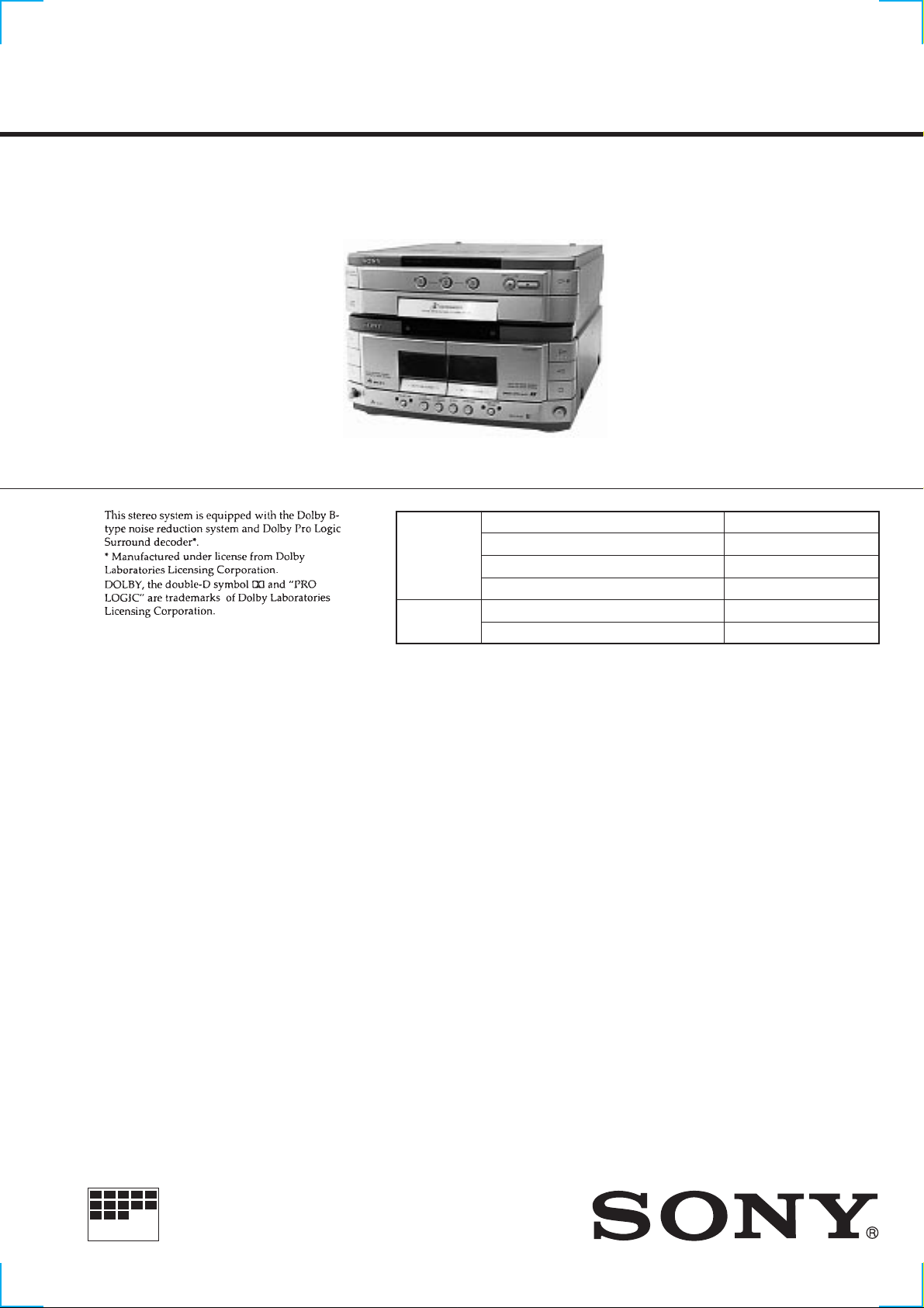
HTC-WX5
SERVICE MANUAL
HTC-WX5 is the deck and CD
section in MHC-WX5/WX7.
Model Name Using Similar Mechanism HTC-W555
CD
SECTION
TAPE DECK
SECTION
CD Mechanism Type CDM38-5BD29A
Base Unit Type BU-5BD29AL
Optical Pick-up Type KSS-213B/S-N
Model Name Using Similar Mechanism HCD-VR90AV
T ape Transport Mechanism Type TCM-230AWR2
E Model
Australian Model
Tourist Model
SPECIFICATIONS
CD player section
System Compact disc and digital audio system
Laser Semiconductor laser ( =780nm)
Emission duration : continuous
Laser output Max. 44.6 µW*
*This output is the value measured at a
distance of 200mm from the objective
lens surface on the Optical Pick-up Block
with 7mm aperture.
Frequency response 20Hz – 20kHz (±1dB)
Wavelength 780 – 790 nm
Signal-to-noise ratio More than 90dB
Dynamic range More than 90dB
CD OPTICAL DIGITAL OUT
(Square optical connector jack, rear panel)
Wavelength 600nm
Output Level -18dBm
Tape player section
Recording system 4-track 2-channel stereo
Frequency response 40 – 13,000Hz (±3dB), using Sony TYPE I
(DOLBY NR OFF) cassette 40 – 14,000Hz (±3dB), using Sony
TYPE II cassette
General
Dimensions (w/h/d) Approx. 288 × 205 × 360mm
Mass Approx. 4.4kg
Design and specifications are subject to change without notice.
COMPACT DISC DECK
MICROFILM
CAUTION
Use of controls or adjustments or performance of procedures
other than those specified herein may result in hazardous
radiation exposure.
Notes on chip component replacement
• Never reuse a disconnected chip component.
• Notice that the minus side of a tantalum capacitor may be
damaged by heat.
Flexible Circuit Board Repairing
• Keep the temperature of soldering iron around 270˚C
during repairing.
• Do not touch the soldering iron on the same conductor of the
circuit board (within 3 times).
• Be careful not to apply force on the conductor when soldering
or unsoldering.
Laser component in this product is capable of emitting radiation
exceeding the limit for Class 1.
This appliance is classified as
a CLASS 1 LASER product.
The CLASS 1 LASER
PRODUCT MARKING is
located on the rear exterior.
NOTES ON HANDLING THE OPTICAL PICK-UP BLOCK
OR BASE UNIT
The laser diode in the optical pick-up block may suffer electrostatic
break-down because of the potential difference generated by the
charged electrostatic load, etc. on clothing and the human body.
During repair, pay attention to electrostatic break-down and also
use the procedure in the printed matter which is included in the
repair parts.
The flexible board is easily damaged and should be handled with
care.
NOTES ON LASER DIODE EMISSION CHECK
The laser beam on this model is concentrated so as to be focused on
the disc reflective surface by the objective lens in the optical pickup block. Therefore, when checking the laser diode emission,
observe from more than 30 cm away from the objective lens.
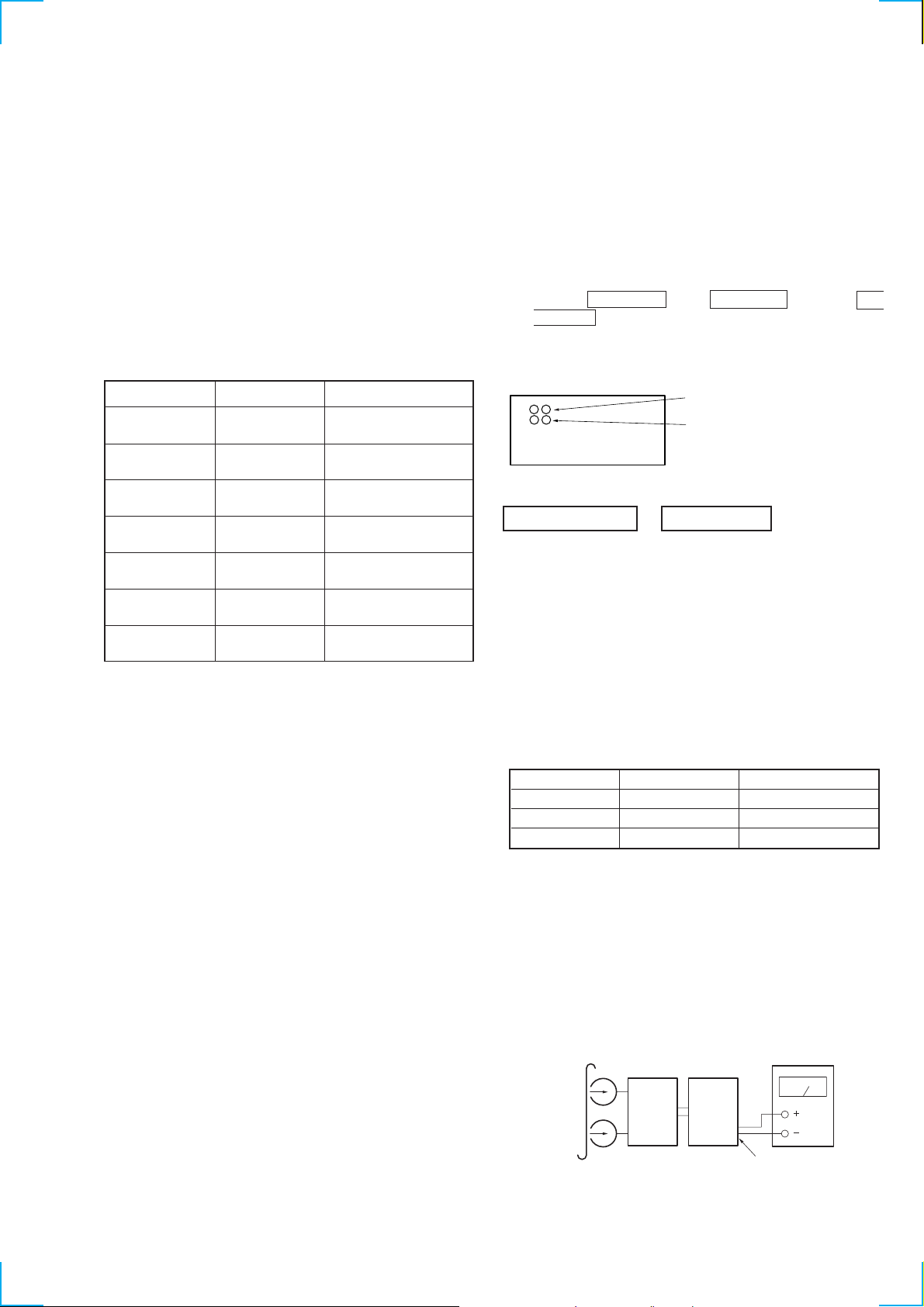
LASER DIODE AND FOCUS SEARCH OPERATION
CHECK
Carry out the “S curve check” in “CD section adjustment” and check
that the S curve waveform is output three times.
SAFETY-RELATED COMPONENT WARNING!!
COMPONENTS IDENTIFIED BY MARK ! OR DO TTED LINE WITH
MARK ! ON THE SCHEMATIC DIAGRAMS AND IN THE PARTS
LIST ARE CRITICAL TO SAFE OPERATION. REPLACE THESE
COMPONENTS WITH SONY PARTS WHOSE PART NUMBERS
APPEAR AS SHOWN IN THIS MANUAL OR IN SUPPLEMENTS
PUBLISHED BY SONY.
2

TABLE OF CONTENTS
1. SERVICING NOTE .......................................................... 4
2. GENERAL ..........................................................................7
3. DISASSEMBLY
3-1. Loading Panel ................................................................. 8
3-2. Back Panel and CD Mechanism Deck ............................ 8
3-3. Front Panel ...................................................................... 9
3-4. TC Mechanism Deck and Cassette Holder ..................... 9
3-5. Disc Tray....................................................................... 10
4. MECHANICAL ADJUSTMENTS ..........................11
5. ELECTRICAL ADJUSTMENTS ...............................11
6. DIAGRAMS
6-1. Circuit Boards Location ................................................14
6-2. Block Diagrams
• CD Section .......................................................................15
• Deck Section .................................................................... 16
• Main Section .................................................................... 14
6-3. Printed Wiring Board CD Section .............................. 18
6-4. Schematic Diagram CD Section ................................ 19
6-5. Schematic Diagram Deck Section .............................. 20
6-6. Printed Wiring Board Deck Section............................ 21
6-7. Printed Wiring Board Main Section............................ 22
6-8. Schematic Diagram Main (1/2) Section...................... 23
6-9. Schematic Diagram Main (2/2) Section...................... 24
6-10. Printed Wiring Board Leaf SW Section.................... 25
6-11. Schematic Diagram Leaf SW Section ...................... 25
6-12. Printed Wiring Board Panel Section ......................... 26
6-13. Schematic Diagram Panel Section ............................ 27
6-14. Schematic Diagram CD Motor Section .................... 28
6-15. Printed Wiring Board CD Motor Section ................. 29
6-16. IC Block Diagrams ..................................................... 30
6-17. IC Pin Functions ......................................................... 32
7. EXPLODED VIEWS
7-1. Case and Back Panel Section........................................39
7-2. Front Panel Section ....................................................... 40
7-3. CD Mechanism Section 1 (CDM38-5BD29A)............. 41
7-4. CD Mechanism Section 2 (CDM38-5BD29A)............. 42
7-5. Base Unit Section (BU-5BD29A)................................. 43
7-6. TC Mechanism Section 1 (TCM230AWR2) ................44
7-8. TC Mechanism Section 2 (TCM230AWR2) ...............45
8. ELECTRICAL PARTS LIST ........................................ 46
3
SECTION 1
SERVICING NOTE
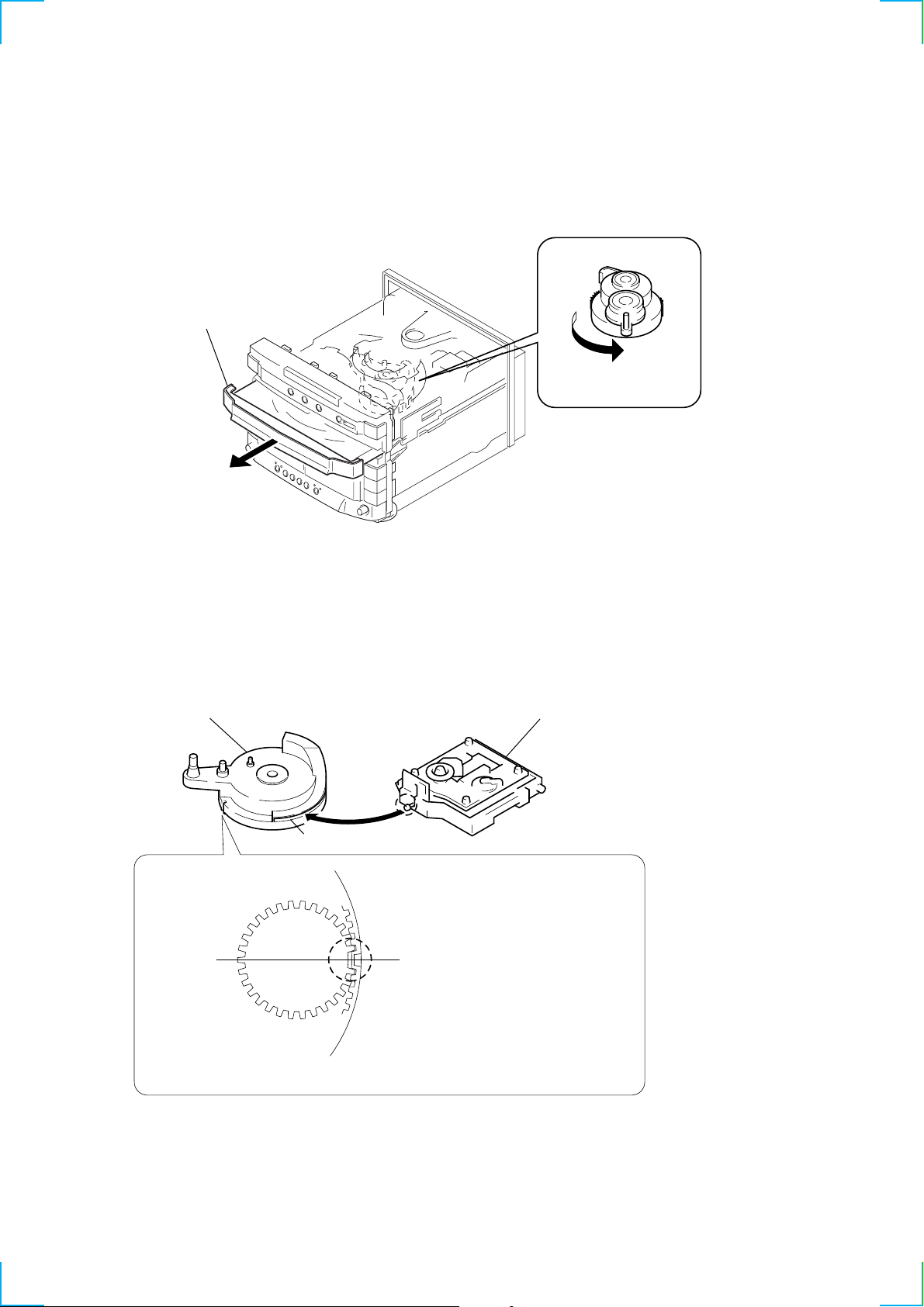
HOW TO OPEN THE DISC TRAY WHEN POWER SWITCH
TURNS OFF
1
Remove the Case.
3
Pull-out the disc tray.
2
Turn the cam to the
direction of arrow.
Note for Installation (ROTARY ENCODER)
BU cam
Groove
Note:When attaching the Base unit, Insert the
section A into the groove of BU cam.
Section A
Note:When attaching the BU cam,
engage the Rotary encoder
switch as shown in the figure.
4
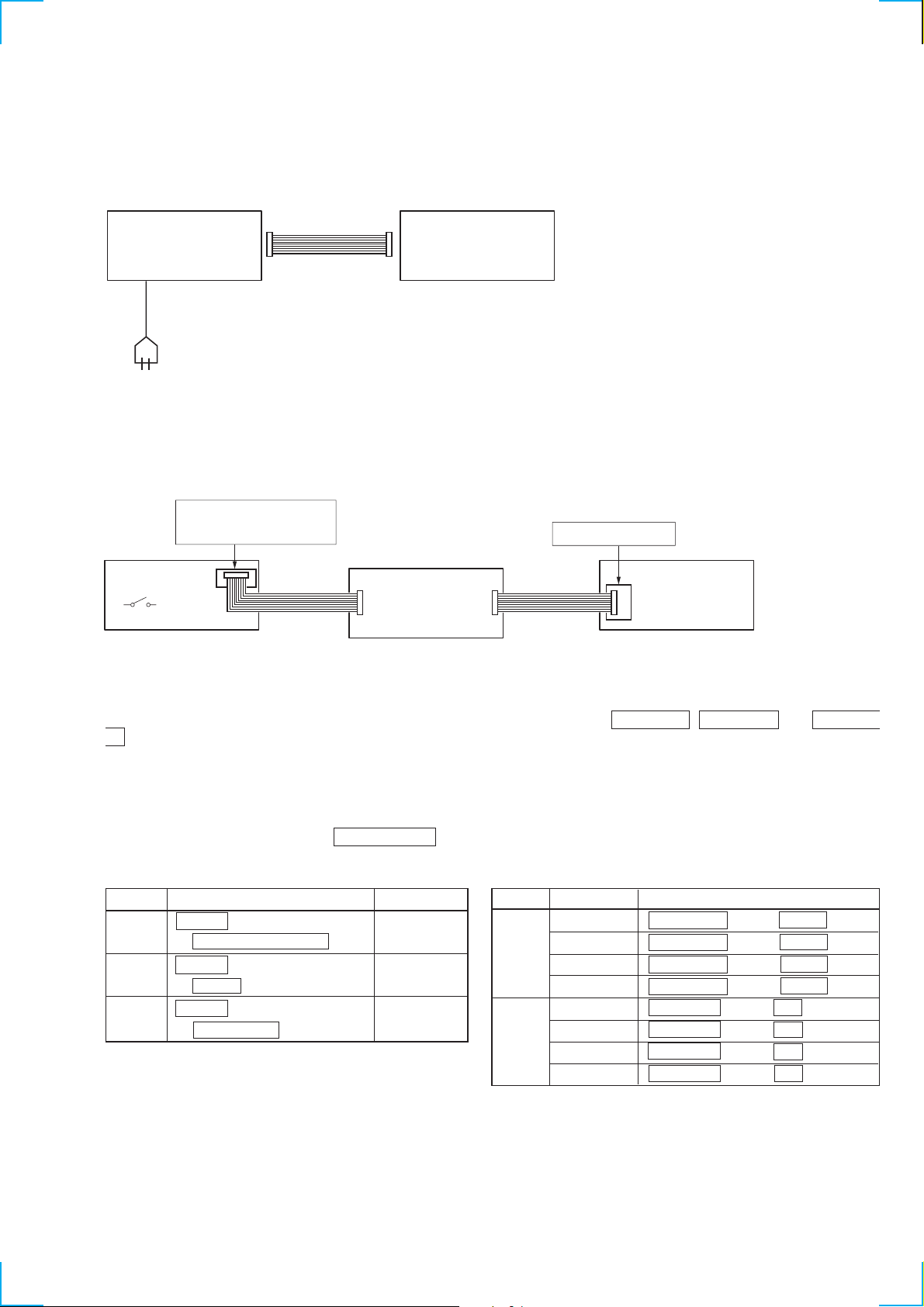
Connection and Operations of the Unit by Itself
This unit cannot be operated by itself as it does not come with a power supply.
Connect STR-WX5/WX7 as shown in “Connection 1” before beginning servicing.
Connection 1: If there is STR-WX5/WX7.
STR-WX5/WX7
SYSTEM CABLE 17P
AC IN
SET
Use a power supply jig (PFJ-1) if the STR-WX5/WX7 is not available.
Connect the conversion jig for connection (J-2501-138-A) as shown in “Connection 2” before beginning servicing.
Connection 2: If there is not STR-WX5/WX7.
FH-E939,838,737
MHC-6600,5600,3600,2600
CDP/TC
Power SW
Service Box (PFJ-1)
Conversion
Jig
(J-2501-138-A)
Connector
cable 17P
(Supplied with PFJ-1)
Conversion Jig or Set)
SYSTEM CONTROL
Set
Connector
cable 17P
(Supplied with
T o operate the unit by itself , turn on the power of the conduction jig (PFJ-1), and press the s (TAPE A) , s (TAPE B) , and H (TAPE
B) buttons together in this order.
As this unit is not equipped with fast forward and rewind buttons, buttons need to be combined and pressed together for different functions
when operating the unit by itself. (See Table-2.)
However, it will not operate properly if operations are performed without switching the functions.
Perform the following procedure to switch the functions before operating the unit.
The function selected is indicated by the DISC NUMBER indicator.
Table 1 Switching the Functions
Function
Operation
Indicator
CD x (CD) button 1< 2< 3
+ HI-SPEED DUBBING button
T APE A x (CD) button 1< 2 3
+ z REC button
TAPE B x (CD) button 12< 3
+ h (TAPE A) button
Table 2 Pressing Combination of Buttons When Operated by Itself
Deck
Function Operation
CD > (AMS) s (TAPE B) button + DISC3 button
. (AMS) s (TAPE B) button + DISC1 button
M s (TAPE A) button + DISC3 button
m s (TAPE A) button + DISC1 button
T APE A > (AMS) DISC SKIP button + H (TAPE B)
TAPE B . (AMS) DISC SKIP button + h (TAPE B)
M DISC SKIP button + H (TAPE A)
m DISC SKIP button + h (TAPE A)
The function can be differentiated by the lighting of this part of the indicator.
↓↓
1< 2< 3
5

Cold Reset
NOTE: This is the mode for operating the unit by itself. Take note that the operating method differs when connected to the STR-WX5/
WX7. This method is described in the manuals of the STR-WX5 and STR-WX7. Refer to these manuals for details.
This mode is used for initializing the RAM contents. Perform this mode when returning the repaired product to the customer.
Precedure:
1. After turning ON the power of the conduction jig (PFJ-1), press the s (TAPE A) button, s (TAPE B) button, and H (TAPE B)
button together in this order.
2. Press the X (TAPE) button while pressing the x (CD) button.
CD Delivery Mode
NOTE: This is the mode for operating the unit by itself. Take note that the operating method differs when connected to the STR-WX5/
WX7. This method is described in the manuals of the STR-WX5 and STR-WX7. Refer to these manuals for details.
This mode moves the pickup to areas where the anti-vibration is stronger. Perform this mode when returning the repaired product
to the customer.
Precedure:
1. After turning ON the power of the conduction jig (PFJ-1), press the s (TAPE A) button, s (TAPE B) button, and H (TAPE B)
button together in this order.
2. Press the CD SYNCHRO button while pressing the x (CD) button.
3. Wait untill z (TAPE B) indicator is on befor disconnect from the conduction jig (PFJ-1).
LED All Lit Mode
NOTE: Always perform this mode when operating the unit by itself.
This mode is used for lighting up the whole LED.
Precedure:
1. After turning ON the power of the conduction jig (PFJ-1), press the s (TAPE A) button, s (TAPE B) button, and H (TAPE B)
button together in this order.
2. The whole LED can be turned on and off each time the s (TAPE A) button is pressed while pressing the x (CD) button.
3. Press the three buttons in step 1 at the end.
Key Check Mode
NOTE: Always perform this mode when operating the unit by itself.
This mode is used for checking the key inputs of the buttons of the unit.
Precedure:
1. After turning ON the power of the conduction jig (PFJ-1), press the s (TAPE A) button, s (TAPE B) button, and H (TAPE B)
button together in this order.
2. Press the DOLBY NR button while pressing the x (CD) b utton to set the ke y check mode, and the indicator displays “ 3 HX”.
3. The number of buttons pressed are indicated in binary digits by the indicator LED. Buttons pressed once are not counted when pressed
again.
4. Press the two buttons in step 2 at the end.
Display: 1< 2< 3
MSB ↑
↑ LSB
Aging Mode
NOTE: Perform the following procedure only when operating the unit by itself.
This mode is used for checking the operations of the CD player and tape deck.
The operations are the same as the aging mode described in the service manual for the STR-WX5/WX7. Howev er as this unit does
not have a fluorescent indicator tube, operating states and error statuses cannot be checked.
If the STR-WX5/WX7 is available, set the aging mode according to those service manuals.
Aging continues in the following sequence as long as no errors occur.
Aging of CD player (12 minutes)
Aging of deck A
Aging of deck B
Aging of deck A (half)
10 minutes
Precedure:
1. After turning ON the power of the conduction jig (PFJ-1), press the s (TAPE A) button, s (TAPE B) button, and H (TAPE B)
button together in this order.
2. Press the s (TAPE B) button while pressing the x (CD) button to set the aging mode and start aging.
3. To end aging, press the three buttons in step 1.
6
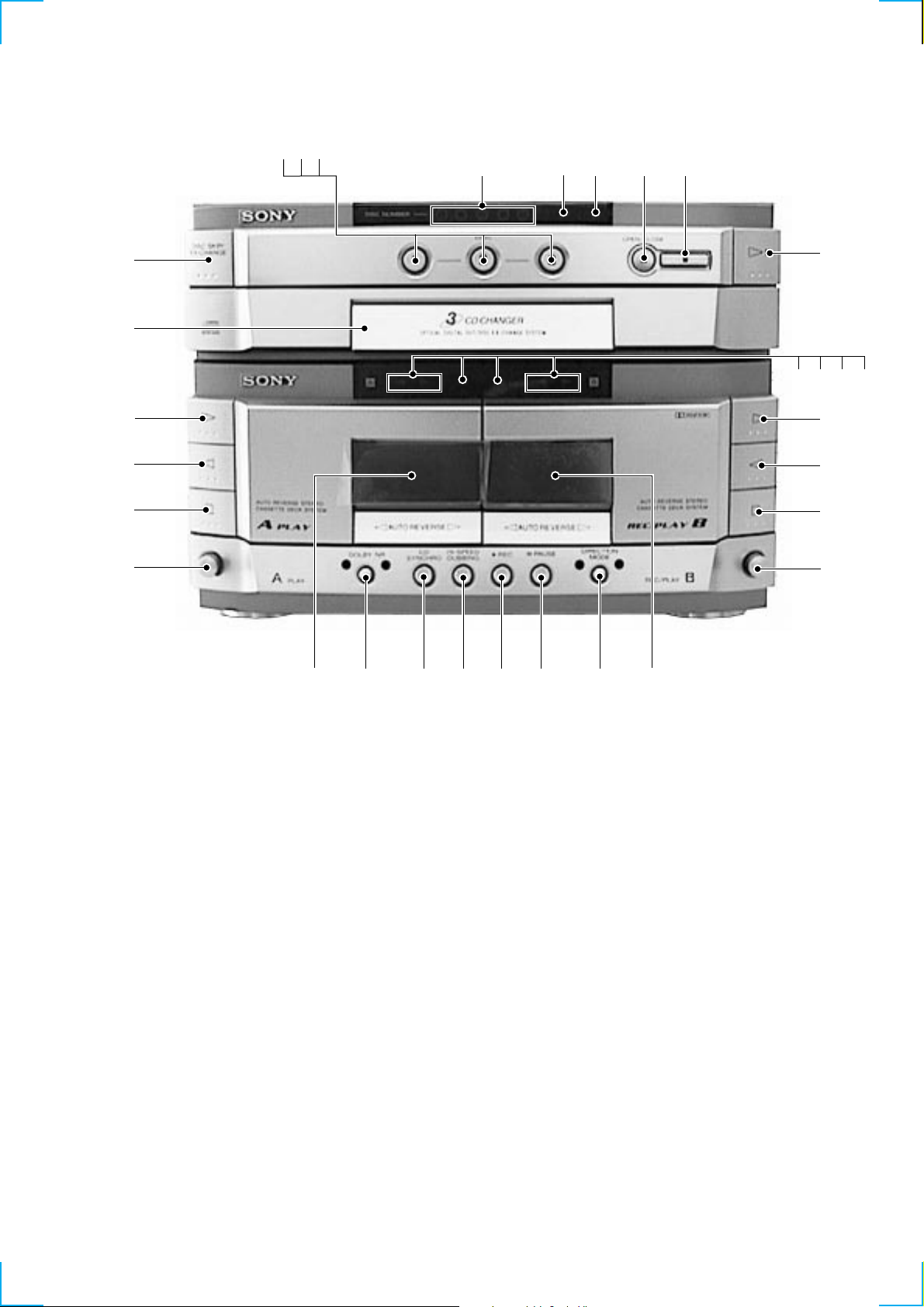
Front Panel
234
5
6
789
0
qa qs qd qf
qg
qh
qj
qk
ql
w;wawswdwfwg
wh
wj
wk
wl
e;
ea
1
SECTION 2
GENERAL
Location of Parts and Controls
1 DISC SKIP/EX-CHANGE button
2 DISC 1 button
3 DISC 2 button
4 DISC 3 button
5 DISC NUMBER 1< 2< 3 indicator
6 N (CD play) indicator
7 X (CD pause) indicator
8 Z OPEN/CLOSE button
9 x (CD stop) button
0 HX (CD play pause) button
qa Y (Deck A play) indicator
qs z (Deck B rec) indicator
qd X (Tape (Deck B pause)) indicator
qf Y (Deck B play) indicator
qg H (Deck B play) button
qh h (Deck B play) button
qj s (Deck B stop) button
qk A (Deck B eject) button
ql Cassette lid (Deck B)
s; DIRECTION MODE button
wa X PAUSE button
ws z REC button
wd HI-SPEED DUBBING button
wf CD SYNCHIRO button
wg DOLBY NR button
wh Cassette lid (Deck A)
wj A EJECT (Deck A) button
wk s (Deck A stop) button
wl h (Deck A play) button
e; H (Deck A play) button
ea CD Disc tray
7
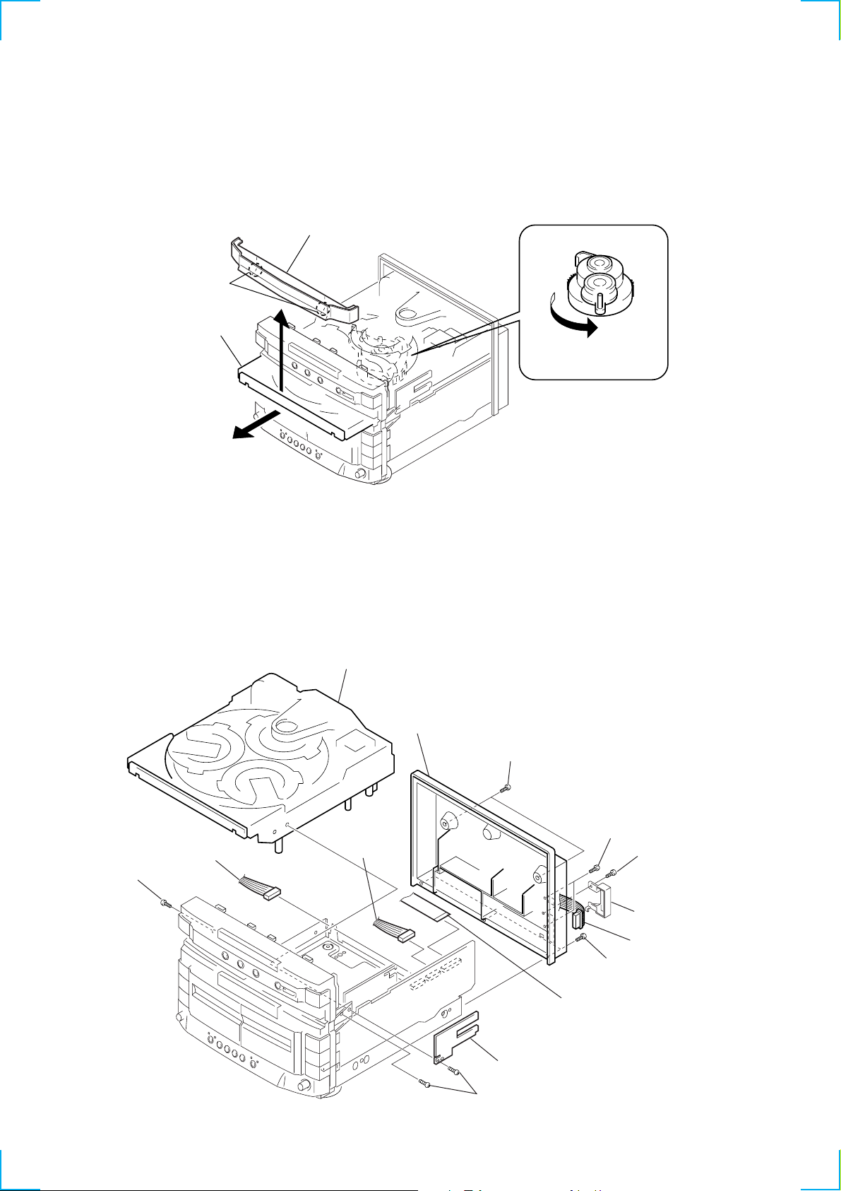
SECTION 3
DISASSEMBLY
Note: Follow the disassembly procedure in the numerical order given.
3-1. LOADING PANEL
3
Loading panel
(Remove two claws)
Two claws
2
Pull-out the disc tray.
1
Turn the cam to the
direction of arrow.
3-2. BACK PANEL AND CD MECHANISM DECK
!¢
CD mechanism deck
!™
(CN111)
!º
Screw
(BVTP3x10)
!£
Connector
(CN112)
7
Connector
Back panel
4
Two screws
(BVTP3x10)
!¡
(19core, CNS103)
6
Two screws
(BVTP3x8)
5
Three screws
(BVTP3x10)
Flat type wire
1
Screw
(BVTP3x8)
2
Cover (SC)
3
System cable
9
Dummy board
8
Two screws
(BVTP3x10)
8
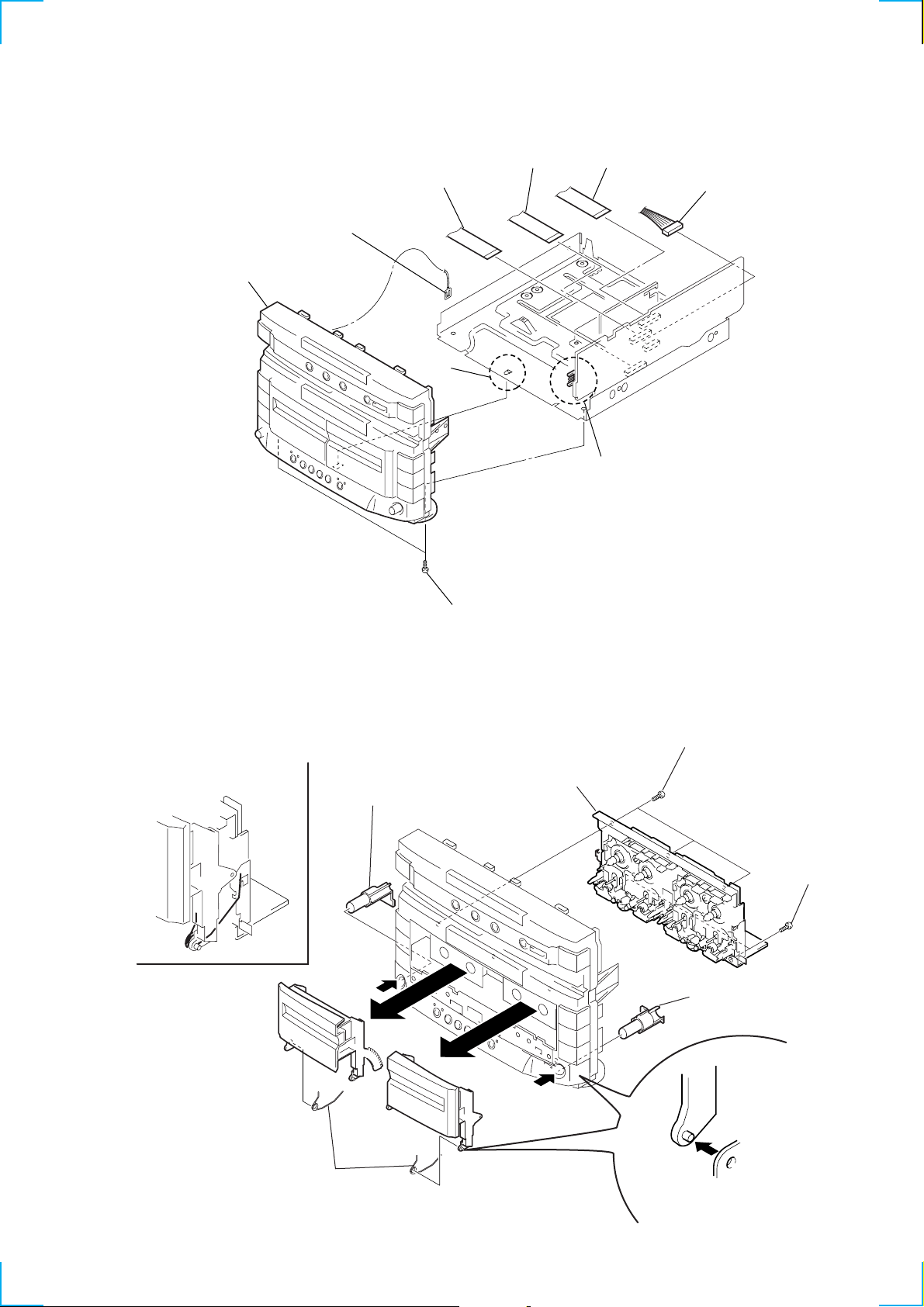
3-3. FRONT PANEL
A
2
Three screws
(BVTP2.6x8)
3
Two screws
(BVTP2.6x8)
4
TC mechanism deck
5
Two springs
C
D
D
C
6
Remove the Cassette holder A
and Cassette holder B.
(Remove C first, and remove D.)
7
Eject button A
8
Eject button B
Note for installation
Set the Spring to be at the position
in the figure.
B
8
Front panel
(Remove the catcer)
3
Flat type wire
(15core, CNS101)
6
Lead (with connector)
2
Flat type wire
(17core, CNS104)
Catcher
1
Flat type wire
(13core, CNS102)
7
Connector (CNP105)
4
Connector
(CN113)
3-4. TC MECHANISM DECK AND CASSETTE HOLDER
1
Push the 6 buttons.
(Arrow A and arrow B.)
5
Two screws
(BVTP3x10)
9
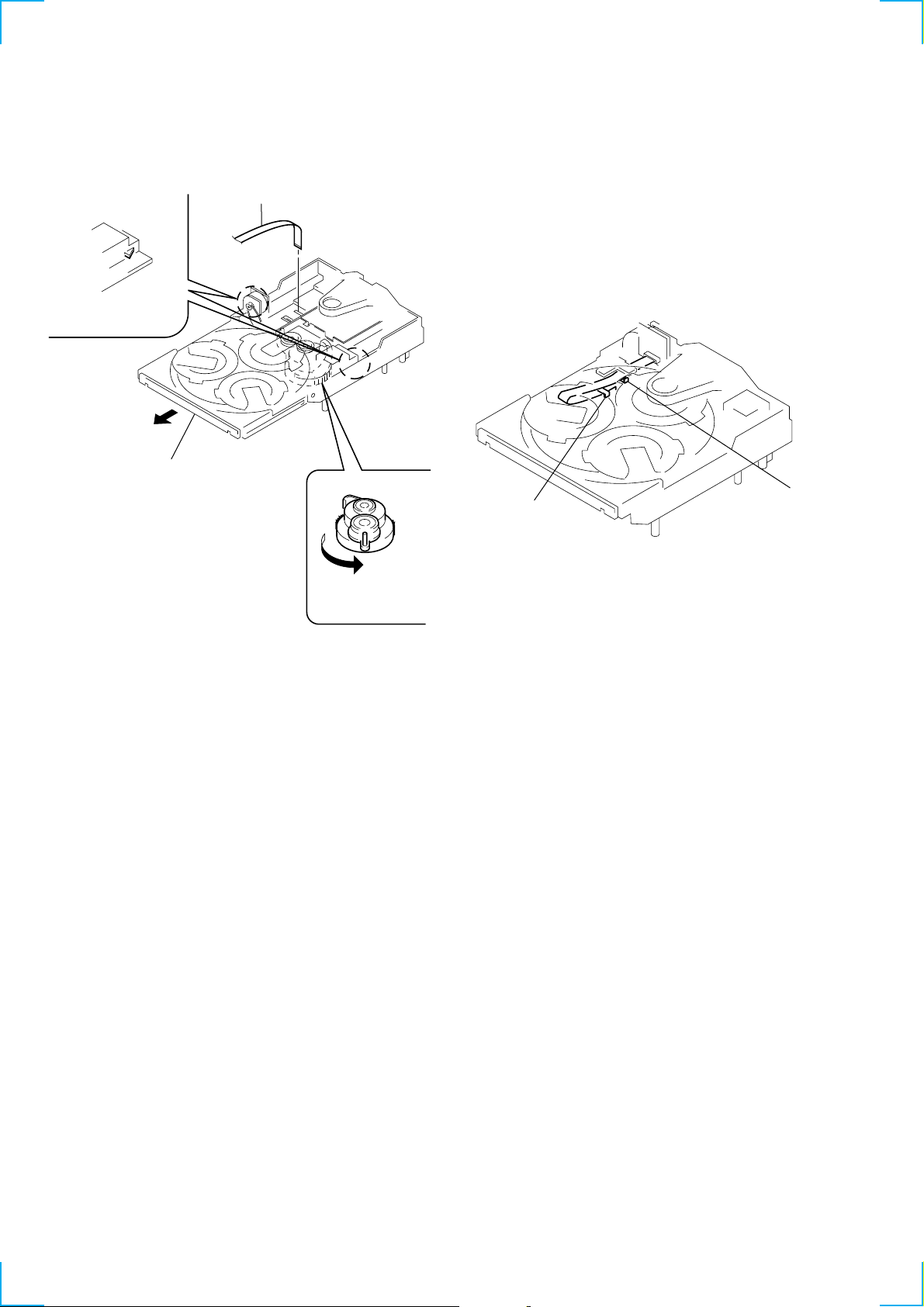
3-5. DISC TRAY
4
Two claws
2
Pull-out the disc tray.
5
Remove the disc tray.
3
Flat type wire (8 core)
Note for installation
When installing the Disc tray, pull around the flat type wire to
pass through the claw A and claw B, as shown in the figure.
Claw
A
Claw
B
1
Turn the cam the
direction of arrow.
10
SECTION 4
MECHANICAL ADJUSTMENTS
SECTION 5
ELECTRICAL ADJUSTMENTS
Precaution
1. Clean the following parts with a denatured alcohol-moistened
swab:
record/playback heads pinch rollers
erase head rubber belts
capstan idlers
2. Demagnetize the record/playback head with a head
demagnetizer.
3. Do not use a magnetized screwdriver for the adjustments.
4. After the adjustments, apply suitable locking compound to the
parts adjusted.
5. The adjustments should be performed with the rated power
supply voltage unless otherwise noted.
Torque Measurement
Mode
FWD
FWD
back tension
REV
REV
back tension
FF/REW
FWD tension
REV tension
Torque meter
CQ-102C
CQ-102C
CQ-102RC
CQ-102RC
CQ-201B
CQ-403A
CQ-403R
Meter reading
31 to 71 g • cm
(0.43 – 0.98 oz • inch)
2 to 6 g • cm
(0.02 – 0.08 oz • inch)
31 to 71 g • cm
(0.43 – 0.98 oz • inch)
2 to 6 g • cm
(0.02 – 0.08 oz • inch)
71 to 143 g • cm
(0.98 – 1.99 oz • inch)
100 g or more
(3.53 oz or more)
100 g or more
(3.53 oz or more)
Read before adjustments
T o adjust the unit, operate the unit by itself using the conduction jig
(PFJ-1).
For details on switching functions and fast forwarding the unit, etc.
when operating it by itself, refer to “Connection and Operations of
the Unit by Itself” on page 5 of Servicing Notes.
• Turning on the power
When operating the unit by itself:
1. After turning ON the power of the conduction tool (PFJ-1),
press the π (T APE A) button, π (T APE B) button, and ·
(TAPE B) button together in this order.
Inputting/outputting audio signals:
Use the jack of the power supply jig (PFJ-1).
Output point
Input point
PFJ-1
DECK SECTION 0 dB=0.775V
1. Demagnetize the record/playback head with a head
demagnetizer.
2. Do not use a magnetized screwdriver for the adjustments.
3. After the adjustments, apply suitable locking compound to the
parts adjusted.
4. The adjustments should be performed with the rated power
supply voltage unless otherwise noted.
5. The adjustments should be performed in the order given in this
service manual. (As a general rule, playback circuit adjustment
should be completed before performing recording circuit
adjustment.)
6. The adjustments should be performed for both L-CH and RCH.
Tape
P-4-A100
WS-48B
P-4-L300
7. Switches and controls should be set as follows unless otherwise
specified.
Record/Playback Head Azimuth Adjustment
(Deck A, Deck B)
Signal Used for
10 kHz, –10 dB
3 kHz, 0 dB
315 Hz, 0 dB
Azimuth Adjustment
Tape Speed Adjustment
Level Adjustment
Note: Perform this adjustments for both decks.
Procedure:
1. Mode : Playback
test tape
P-4-A100
(10kHz, -10dB)
set
PFJ-1
output point
level meter
11
)
2. Turn the adjustment scre w and check output peaks. If the peaks
e
do not match for L-CH and R-CH, turn the adjustment screw
so that outputs match within 1 dB of peak.
Tape Speed Adjustment (Deck B)
Note: Set the test mode using the following method and begin tape
speed adjustment.
In the test mode, the speed will switch to double speed or
normal speed each time the HI-SPEED DUBBING button
is pressed.
L-CH
peak
R-CH
screw
position
peak
3. Mode: Playback
test tape
P-4-A100
(10kHz, -10dB)
output
within
level
1 dB
L-CH
peak
output point
set PFJ-1
Waveform of oscilloscope
R-CH
peak
oscilloscop
within 1dB
screw
position
Procedure:
Press the p (CD) button while pressing the DIRECTION MODE
button.
1. Insert the WS-48B into deck B, while pressing the p (CD)
button, press the ª (TAPE A) button, set the function to
“deck B”.
2. Press the · button of deck B.
3. Press the HI-SPEED DUBBING button and play the tape at
double speed.
4. Adjust RV1001 of the LEAF SW board so that the reading of
the frequency counter becomes 6000 ± 180 Hz.
5. Press the HI-SPEED DUBBING button and play the tape at
normal speed.
6. Adjust RV1002 of the LEAF SW board so that the reading of
the frequency counter becomes 3000 ± 90 Hz.
Adjustment Location: LEAF SW board
Sample Value of Wow and flutter
W.RMS (JIS) less than 0.3%
(test tape: WS-48B)
Playback Level Adjustment (Deck A, Deck B)
Procedure:
Mode: Playback
in phase 45
good
°
135
90
°
°
wrong
180
°
4. After the adjustments, apply suitable locking compound to the
parts adjusted.
Adjustment Location: Playback Head (Deck A)
Record/Playback/Erase Head (Deck B)
Reverse
test tape
P-4-L300
(315Hz, 0dB)
set
PFJ-1
level meter
output point
Deck A is RV311 (L-CH) and RV411 (R-CH), deck B is RV301
(L-CH) and RV401 (R-CH)
so that adjustment within the following adjustment level.
Adjustment level:
Output point from PFJ-1 playback level: 301.5 to 338.3 mV (–8.2
to –7.2 dB)
level difference between the channels: within ± 0.5 dB
Adjustment Location: AUDIO board
Adjustment Location
[LEAF SW BOARD]
RV1001(High Speed)
RV1002(Normal Speed
12
Forward
RV1002 RV1001
HTC-WX5
VOLT/DIV : 200mV
TIME/DIV : 500ns
level : 1.3
±
0.3 Vp-p
Record Bias Adjustment (Deck B)
Procedure:
1. Press the p (CD) button while pressing the DIRECTION
MODE button.
2. While pressing the p (CD) button, press the ª (T APE A)
button, set the function to “deck B”.
3. Insert a tape into deck B, press the r REC button, and then
press the ( button to start recording.
4. Mode: Record
INPUT POINT
AF OSC
attenuator
1) 315 Hz
2) 10 kHz
600
Ω
PFJ-1
} 50 mV (–23.8 dB)
blank tape
CS-123
set
5. Mode: Playback
recorded
position
PFJ-1
set
level meter
output
point
6. Confirm playback the signal recorded in step 2 become
adjustment level as follows.
If these levels do not adjustment level, adjust the RV341 (LCH) and R V441 (R-CH) on the A UDIO board to repeat steps 3
and 4.
Adjustment level: The playback output of 10 kHz le vel dif ference
against 315 Hz reference should be ± 1.0 dB.
Adjustment Location: AUDIO board
[AUDIO BOARD] (Component Side)
Record Level Adjustment (Deck B)
Procedure:
1. Press the p (CD) button while pressing the DIRECTION
MODE button.
2. While pressing the p (CD) button, press the ª (TAPE A)
button, set the function to “deck B”.
3. Insert a tape into deck B, press the r REC button, and then
press the ( button to start recording.
4. Mode: Record
INPUT POINT
AF OSC
attenuator
315Hz 50 mV (–23.8 dB)
600
Ω
PFJ-1
set
blank tape
CS-123
5. Mode: Playback
recorded
position
PFJ-1
set
level meter
output
point
6. Confirm playback the signal recorded in step 2 become
adjustment level as follows.
If these levels do not adjustment level, adjust the RV301 (LCH) and RV351 (R-CH) on the MAIN board to repeat steps 3
and 4.
Adjustment level: Output point from PFJ-1 playback level: 47.2
to 53.0 mV (–24.3 to –23.3 dB)
Adjustment Location: MAIN board
[MAIN BOARD] (Component Side)
CD SECTION
Note:
1. CD Block is basically constructed to operate without
adjustment. Therefore, check each item in order given.
2. Use YEDS-18 disc (3-702-101-01) unless otherwise indicated.
3. Use an oscilloscope with more than 10MΩ impedance.
4. Clean the object lens by an applicator with neutral detergent
when the signal level is low than specified value with the
following checks.
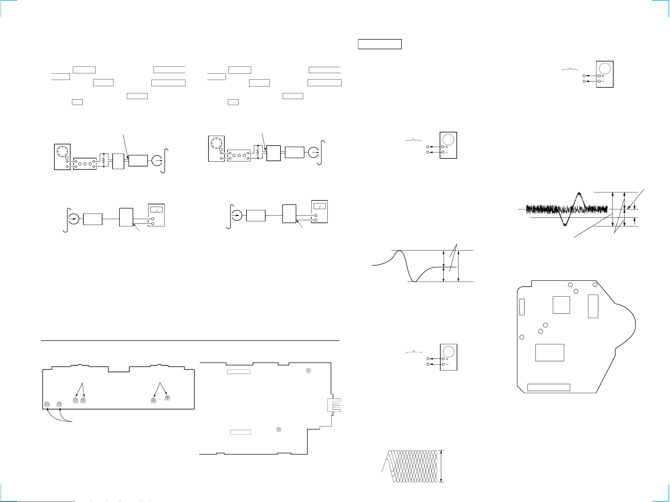
S Curve Check
oscilloscope
BD board
TP (FEO)
TP (VC)
Procedure :
1. Connect oscilloscope to test point TP (FEO).
2. Connect between test point TP (FOK) and Ground by lead wire.
3. Turn Power switch on.
4. Put disc (YEDS-18) in and turned Power switch on again and
actuate the focus search. (actuate the focus search when disc
table is moving in and out.)
5. Check the oscilloscope waveform (S-curve) is symmetrical
between A and B. And confirm peak to peak level within 3 ±
1Vp-p.
S-curve waveform
6. After check, remove the lead wire connected in step 2.
Note: • Try to measure several times to make sure than the ratio of
A : B or B : A is more than 10 : 7.
• T ake sweep time as long as possible and light up the brightness to obtain best waveform.
RF Level Check
BD board
TP (RF)
TP (VC)
symmetry
A
B
oscilloscope
Within 3
±
1 Vp-p
E-F Balance (1 Track Jump) check
oscilloscope
BD board
TP (TEO)
TP (VC)
Procedure:
1. Connect oscilloscope to test point TP (TEO) on BD board.
2. Turned Power switch on.
3. Put disc (YEDS-18) in to play the number five track.
4. Press the “P (Pause)” button.
5. Check the level B of the oscilloscope's waveform and the A
(DC voltage) of the center of the Traverse waveform.
Confirm the following:
• A/B x 100 = less then ± 7 (%)
• B = 500 ± 100 mVp-p
1 track jump waveform
Center of the waveform
B
0V
level : 500 mV
±
100 mVp-p
Symmetry
A (DC voitage)
Adjustment Location:
[BD BOARD] (Conductor Side)
TP (RF)
IC101
CN101
TP
(TEO)
TP
(FEO)
TP
(GND)
IC103
TP
(VC)
TP
(FOK)
IC102
RV341(Lch),RV441(Rch)
Record Bias
RV301 RV401
RV441 RV341
RV301(Lch),RV401(Rch)
Playback Level (Deck B)
RV311(Lch),RV411(Rch)
Playback Level (Deck A)
RV411
RV311
CNS102
CNS101
RV351
Record
Level (R ch)
RV301
Record
Level (L ch)
CNP105
Procedure :
1. Connect oscilloscope to test point TP (RF) on BD board.
2. Turned Power switch on.
3. Put disc (YEDS-18) in and playback.
4. Confirm that oscilloscope waveform is clear and check RF
signal level is correct or not.
Note: Clear RF signal waveform means that the shape “◊” can be
clearly distinguished at the center of the waveform.
RF signal waveform
1313
IC102
HTC-WX5
d
SECTION 6
DIAGRAMS
6-1. CIRCUIT BOARDS LOCATION
CD (P) board
TC LED board
TC (A) board
TC (P) board
CONNECTOR board
TC (B) board
MOTOR (TURN) board
REGULATOR boar
MAIN board
THIS NOTE IS COMMON FOR PRINTED WIRING
BOARDS AND SCHEMATIC DIAGRAMS.
(In addition to this, the necessary note is printed
in each block.)
For schematic diagrams.
Note:
• All capacitors are in µF unless otherwise noted. pF: µµF
50 WV or less are not indicated except for electrolytics
and tantalums.
• All resistors are in Ω and 1/
specified.
¢
•
• 1 : fusible resistor.
• C : panel designation.
Note: The components identified by mark ! or dotted line
• U : B+ Line.
• V : B– Line.
• H : adjustment for repair.
• Voltages and waveforms are dc with respect to ground
• Voltages are taken with a VOM (Input impedance 10 M Ω).
• Waveforms are taken with a oscilloscope.
• Circled numbers refer to waveforms.
• Signal path.
: internal component.
with mark ! are critical for safety.
Replace only with part number specified.
under no-signal (detuned) conditions.
Voltage variations may be noted due to normal produc-
tion tolerances.
Voltage variations may be noted due to normal produc-
tion tolerances.
F : FM
f : AM
E : PB (DECK A)
d : PB (DECK B)
G : REC (DECK B)
J : CD
c : digital out
4
W or less unless otherwise
• Wavef orm
CD SECTION
1
500mV/DIV, 500nsec/DIV
IC101 #£ RFO
2
200mV/DIV, 1µsec/DIV
IC101 2 FEI
3
50mV/DIV, 1msec/DIV
IC101 $¶ TEI
4
IC103 @¶ MDP
5
230µsec
IC103 ^º XPCK
6
1.3Vp-p
0.5Vp-p
0.2Vp-p
7.8µsec
2.5Vp-p
5Vp-p
135µsec
SENSOR board
LEAF SW board
AUDIO board
BD board
MOTOR (SLIDE) board
For printed wiring boards.
Note:
• X : parts extracted from the component side.
• p : parts mounted on the conductor side.
®
•
• b : Pattern from the side which enables seeing.
(The other layers' patterns are not indicated.)
: Through hole.
• Indication of transistor
C
Q
These are omitted
EB
C
EB
These are omitted
IC103 ^™ RFCK
7
IC103 &¢ WFCK
135µsec
8
16.9344MHz
IC103 *ª XTAI
MAIN (2/2) SECTION
9
5MHz
IC101 0 X2
5Vp-p
5Vp-p
2.6Vp-p
5.5Vp-p
1414
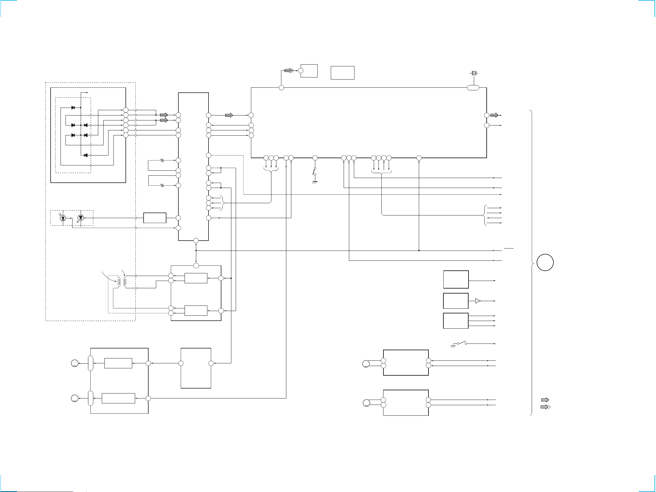
6-2. BLOCK DIAGRAM
CD SECTIOAN
OPTICAL PICK-UP BLOCK
B+
K
E
A
D
A
B
D
C
C
B
F
LASER
DIODE
DETECTOR
HTC-WX5
IC107
1
D.OUT
FOCUS/TRACKING SERVO.
RF AMP
IC101 (1/2)
1
4
2
5
10
6
LD DRIVE
Q101
38
39
41
42
2
1
45
47
3637LD
PD1
PD2
F
E
FEI
FEO
TEO
TEI
PD
SENS1
SENS2
XRST
23
RF O
LOCK
C.OUT
FE O
FE M
TA M
TA O
DATA
XLT
CLK
FOK
33
19
24
25
26
6
7
12
13
22
21
20
27
RF
44
LOCK
29
14
CNIN
15
SEIN
DATAO
XLTO
15 16 17
71
CLKO
DOUT
27
MDP
23
FOK
SPOD
21
CD DIGITAL
OUT
OPTICAL
DIGITAL SIGNAL PROCESSOR
S101
LIMIT
IC103
DATA
10 11 12 75
XLAT
CLOK
SQCK
SENS
SCOR
SQSO
79 100
8
XRST
89 • 90
XTAI
LOUT1
LOUT2
16.9344MHz
•
XTAO
X101
86
93
L-CH
R-CH
CD CLK
CD DATA
SENS2
SCOR
SQ DATA
SQ CLK
SENS
M102
SLED MOTOR
M101
SPINDLE
MOTOR
16
XRST
TRACKING
FOCUS
COIL
11
M
•
12
13
M
•
14
COIL
2-AXIS
DEVICE
SLED/SPINDLE
MOTOR DRIVE
IC102 (2/2)
SLED MOTOR
DRIVE
SPINDLE MOTOR
DRIVE
T+
–
T
–
F
F+
6
3
15
16
18
17
9
MUTE
TRACKING
COIL DRIVE
FOCUS/TRACKING
COIL DRIVE
IC102 (1/2)
FOCUS
COIL DRIVE
SLED
SERVO
IC101 (2/2)
SL P
SL O
S801
DET
TABLE
SENSOR
IC702
DISC
SENSOR
IC703
ROTARY
ENCODER
S811
Q701
27
26
TURN
MOTOR DRIVER
IC701
M701
1416
TURN
MOTOR
M801
SLIDE
MOTOR
M
7
OUT1
2
OUT2
SLIDE
MOTOR DRIVER
IC801
4
M
OUT2
7
OUT1
IN1
IN2
RIN
FIN
OPEN/CLOSE
3
6
2
10
XLAT
T. SENS
DISC SENS
ENC 1
ENC 2
ENC 3
OPEN
TBL.L
TBL.R
LOAD IN
LOAD OUT
A
MAIN
SECTION
(Page 17)
• R CH: Same as L ch
• SIGNAL PATH
: CD
: Digital out
1515
HTC-WX5
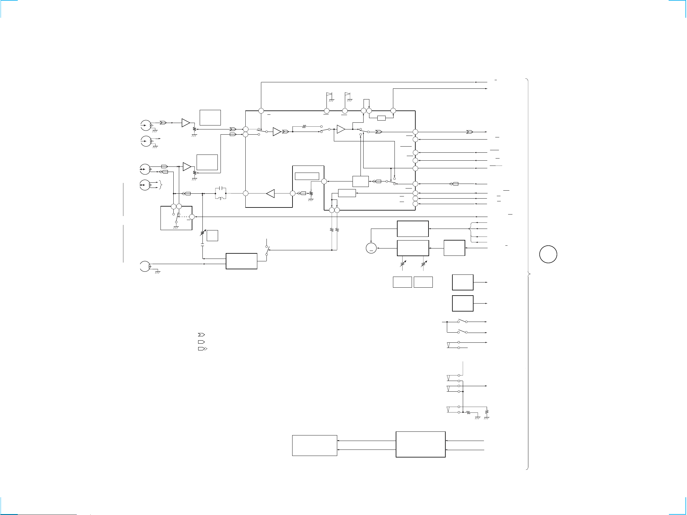
DECK SECTION
HP101
PB HEAD
(DECK A)
REC/PB HEAD
(DECK B)
HRPE101
ERASE HEAD
PB A/B
MS OUT
PB L
LM ON/OFF
NORM/HIGH
NR ON/OFF
REC/PB/PASS
REC L
BIAS ON/OFF
RM ON/OFF
ALC ON/OFF
RELAY REC/PB
CAPM EMG (+)
CAPM EMG (–)
CAPM ON/OFF (+)
CAPM ON/OFF (–)
CAP M H / L
A SHUT
B
MAIN
SECTION
(Page 17)
17
2
DOLBY NR
RECOUT
C
32 33
S1008
B CrO
19
B 120/70
PAS
BIAS SW
M
2
DOL
DOLBY
TYPE B
M1
CAPSTAN
MOTOR
28
27
M
MS
26
PB OUT
LM ON/
OFF
NORM/
HIGH
NR ON/
OFF
PB
BIAS ON/OFF
RM ON/OFF
ALC ON/OFF
CAP MOTOR
CONTROL
Q336-343
RV1002
NORMAL
SPEED
40
25
18
23
24
RIN
44
20
22
15
SPEED
CONTROL
Q1001
RV1001
HIGH
SPEED
SWITCH
Q335
REEL
DETECT
IC1001
S1004
A CrO
RV311
4
PLAYBACK
LEVEL
DECK A
RV301
PLAYBACK
LEVEL
DECK B
RV341
REC
BIAS
REC BIAS
BIAS OSC
T621, Q621, 622
IC611
L
R
L
R
X
R CH
R CH
3
P
ERASE BIAS
IC601
1
IC602
R
REC/PB
16
PB-A/B
A IN
48
B IN
46
RV301
REC LEVEL
+7.5V
Q623
EQIN
38
EQOUT
36
70
120
DOLBY NR
IC301
A 120/70
39
REEL
DETECT
IC1002
S1001 (A PLAY)
• R CH : Same as L ch
• SIGNAL PATH
+5V
S1002 (B PLAY)
: PB (DECK A)
: PB (DECK B)
: REC (DECK B)
16
• PLUNGER SOLENOID is supplied
as the MECHANICAL BLOCK ASSY.
A DECK/
B DECK
PLUNGER
TRIGGER
MOTOR
CONTROL
Q331-334
S1003
(A HALF)
S1005
(REC A)
S1006
(B HALF)
S1009
(REC B)
+5V
+5V
B SHUT
A PLAY
B PLAY
B HALF
B TRIG
A TRIG
1616
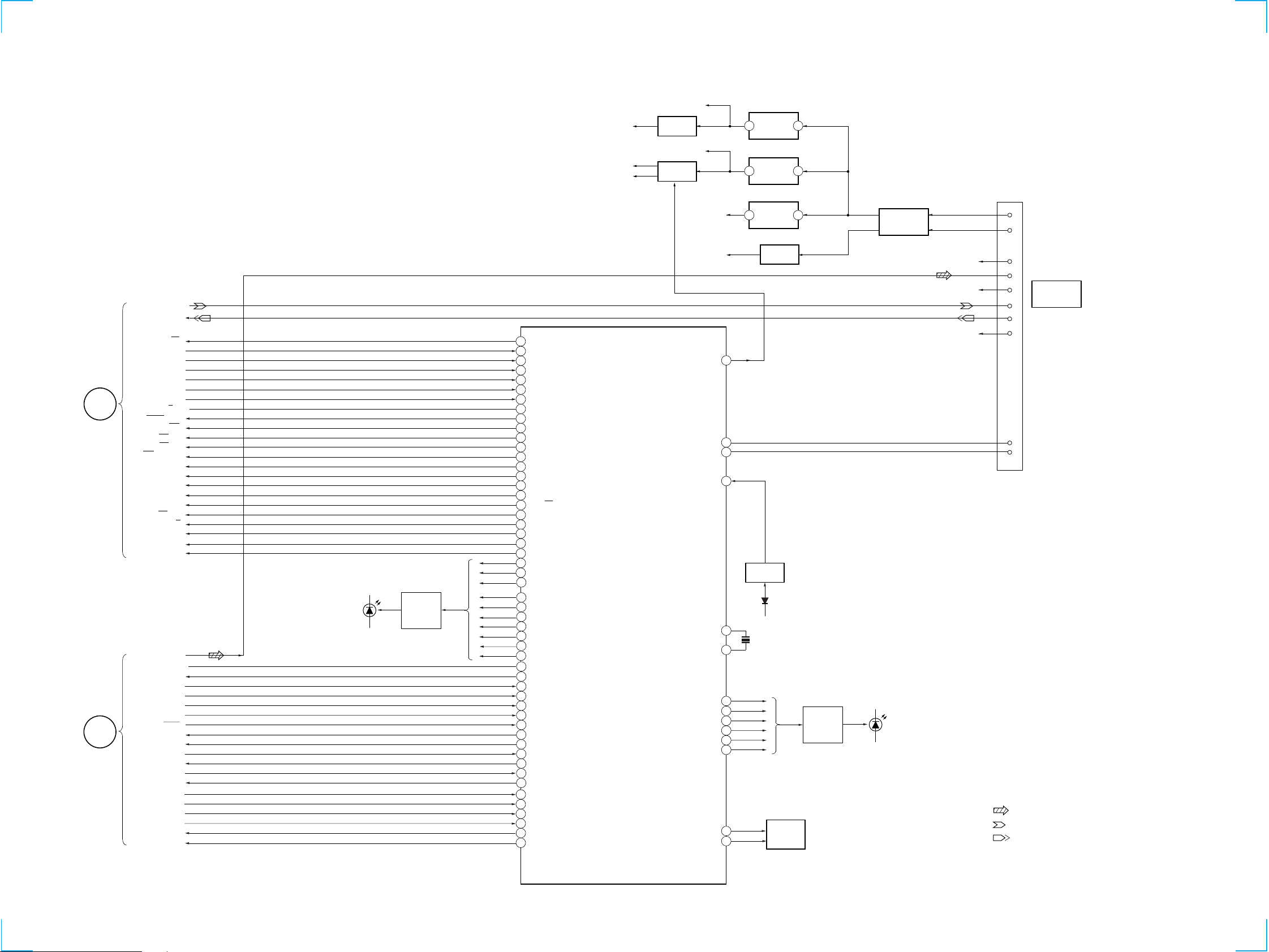
MAIN SECTION
A+7.5V
D+5V
A+5V
+7.5V REG
Q852
+5V SW
Q102-104
M12V
+5V
+12V REG
3 1
IC851
+5V REG
3 1
IC852
HTC-WX5
B
DECK
SECTION
(Page 16)
A
CD
SECTION
(Page 15)
PB L
REC L
RELAY REC/PB
A SHUT
B SHUT
B HALF
A HALF
A PLAY
B PLAY
PB A / B
NORM/HIGH
BIAS ON/OFF
RM ON/OFF
NR ON/OFF
REC/PB PASS
CAPM EMG(-)
CAPM ON/OFF(-)
CAPM ON/OFF(+)
CAPM EMG(+)
ALC ON/OFF
LM ON/OFF
CAP M H/L
A TRG
B TRG
MS OUT
L CH
TBL. L
TBL. R
SCOR
T. SENS
SENS 2
SENS
X RST
CD CLK
CD DATA
DISC SENS
SQ CLK
SQ DATA
X LAT
OPEN
ENC 1
ENC 2
ENC 3
LOAD IN
LOAD OUT
D224-230
LED
ON/OFF
SWITCH
Q214-223
97
TC RELAY
26
A SHUT
27
B SHUT
28
B HALF
98
A HALF
95
A PLAY
96
B PLAY
94
PB A/B
93
NORM/HI
BIAS
92
90
REC MUTE
89
NR ON/OFF
REC/PB
88
CAPM-EMG(-)
85
CAPM ON/OFF(-)
86
100
CAPM ON/OFF(+)
CAPM EMG(+)
1
99
ALC ON/OFF
TC MUTE
87
82
CAPM-H/N
84
A TRG
83
B TRG
31
AMS IN
DECO1
52
66
DECO2
CD-PAUSE
65
67
CD-PLAY
72
DISC1
DISC2
54
DISC3
70
69
EXIST1
53
EXIST2
68
EXIST3
60
TBL L
61
TBL R
SCOR
18
76
T SENS
73
SENSE 2
74
SENS
57
XRST
48
CD CLK
47
CD DATA
75
DISC SENS
36
SQ CLK
34
SQ DATA IN
58
XLAT
OPEN
81
ENC1
80
ENC2
79
ENC3
78
LOAD IN
64
LOAD OUT
63
MASTER CONTROL
IC101
M+7V
A-7.5V
CD-POWER
IIC DATA
IIC CLK
RESET
LED1
LED2
LED3
LED4
LED5
LED6
KEY A
KEY B
+7V REG
3
46
55
56
15
RESET
IC101
D110
X1
11
10
X2
+5V
X101
5MHz
2
3
4
5
6
7
IC853
-7.5V REG
Q855
1
LED
ON/OFF
SWITCH
Q201-206
+
-
D201-206
RECT
D901-904
(CD R)
R CH
(PB R)
R CH
(REC R)
R CH
17
13
3
CNB108
2
9
SYSTEM
CONTROL
7
6
4
14
16
TO
STR-W555
• R CH: Same as L ch
• SIGNAL PATH
: CD
29
30
KEY
MATRIX
: PB
: REC
16
1717
 Loading...