

Sony HTCVX-500 Service manual
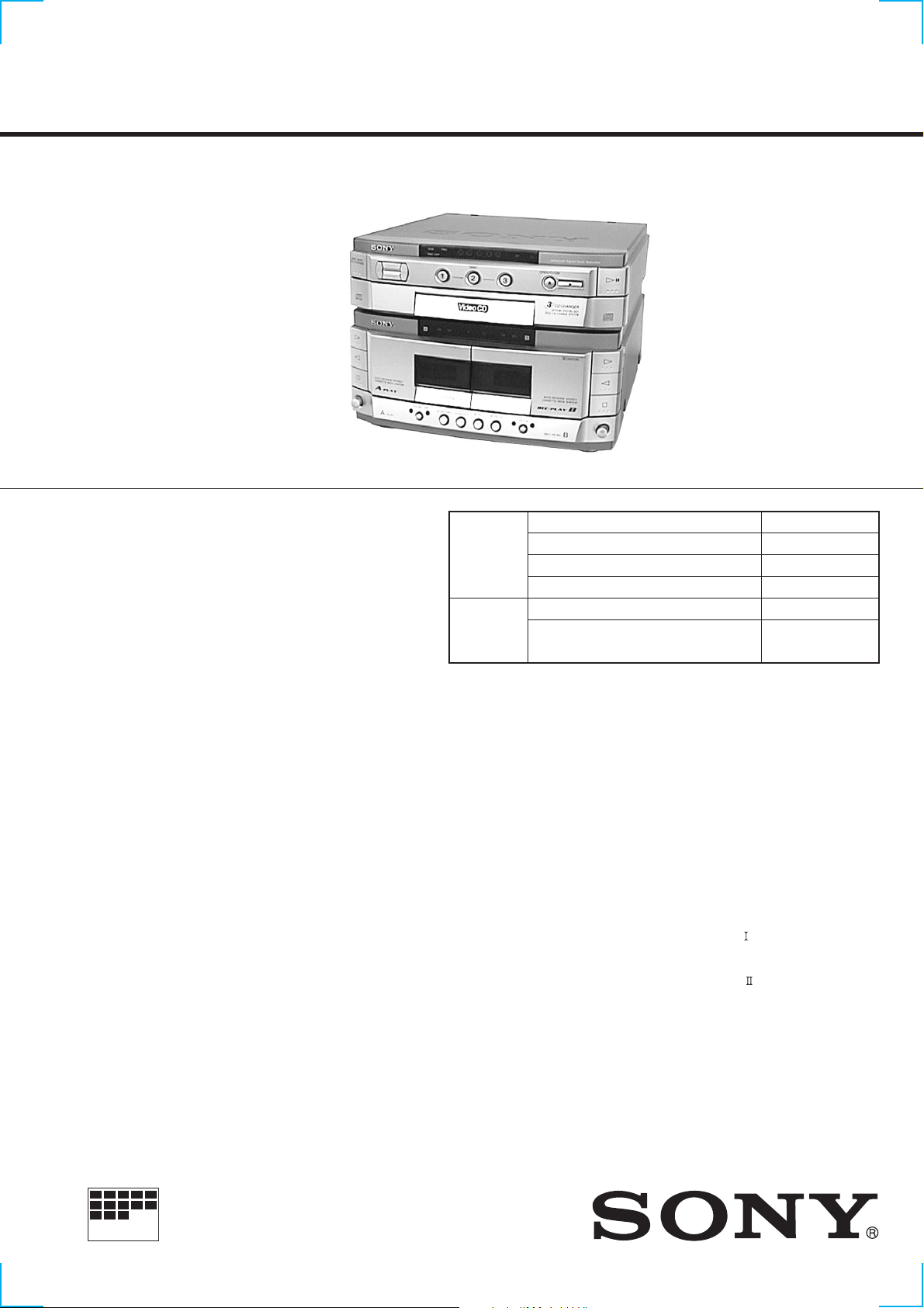
HTC-VX500
SERVICE MANUAL
• This set is the deck and Video CD
section in MHC-VX500/VX700AV.
This stereo system is equipped with the Dolby Btype noise reduction system.
* Manufactured under license from Dolby
Laboratories Licensing Corporation.
DOLBY, the double-D symbol ; and “PR O LOGIC”
are trademarks of Dolby Laboratories Licensing
Corporation.
CD CD Mechanism Type CDM38-5BD24
Section Base Unit Type BU-5BD24
Tape deck
Section
E Model
Model Name Using Similar Mechanism HTC-V5550
Optical Pick-up Name KSS-213BA/F-NP
Model Name Using Similar Mechanism HTC-V5550
T ape Transport Mechanism T ype
TCM-230AWR2
TCM-230PWR2
SPECIFICATIONS
Video section
Inputs AV INPUT VIDEO (phono jack):
1Vp-p, 75 Ω
VIDEO IN (phono jack)
1Vp-p, 75 Ω
Outputs MONITOR OUT (phono jack):
1Vp-p, 75 Ω
VIDEO OUT (phono jack)
1Vp-p, 75 Ω
S-VIDEO (4-pin/mini-DIN jack):
Y: 1Vp-p, unbalanced, sync negative
C: 0.286Vp-p, load impedance 75 Ω
VIDEO CD/CD player section
System Compact disc, digital audio and video
system
Laser Semiconductor laser (λ=780nm)
Emission duradon: continuous
Laser output Max. 44.6µW*
*This output is the value measured at a
diatance of 200 mm from the objective
lens surface on the Optical Pick-up Block
with 7 mm aperture.
Frequency response 20 Hz – 20 kHz (±1 dB)
Wavelength 780 – 790 nm
Signal to noise ratio More than 90 dB
Dynamic range More than 90 dB
Video Color System format
NTSC, P AL
CD OPTICAL DIGITAL OUT
(Square optical connector jack, rear panel)
Wavelength 600 nm
Output Level –18 dBm
Tape player section
Recording system 4-track 2-channel stereo
Frequency response 40 – 13,000 Hz (±3 dB),
(DOLBY NR OFF) using Sony TYPE
cassette
40 – 14,000 Hz (±3 dB),
using Sony TYPE
cassette
General
Dimensions (w/h/d) Approx. 288 × 205 × 360 mm
Mass Approx. 4.6 kg
Design and specifications are subject to change without notice.
COMPACT DISC DECK
MICROFILM
CAUTION
Use of controls or adjustments or performance of procedures
other than those specified herein may result in hazardous
radiation exposure.
Notes on chip component replacement
• Never reuse a disconnected chip component.
• Notice that the minus side of a tantalum capacitor may be
damaged by heat.
Flexible Circuit Board Repairing
• Keep the temperature of soldering iron around 270˚C
during repairing.
• Do not touch the soldering iron on the same conductor of the
circuit board (within 3 times).
• Be careful not to apply force on the conductor when soldering
or unsoldering.
Laser component in this product is capable of emitting radiation
exceeding the limit for Class 1.
NOTES ON HANDLING THE OPTICAL PICK-UP BLOCK
OR BASE UNIT
The laser diode in the optical pick-up block may suffer electrostatic
break-down because of the potential difference generated by the
charged electrostatic load, etc. on clothing and the human body.
During repair, pay attention to electrostatic break-down and also
use the procedure in the printed matter which is included in the
repair parts.
The flexible board is easily damaged and should be handled with
care.
NOTES ON LASER DIODE EMISSION CHECK
The laser beam on this model is concentrated so as to be focused on
the disc reflective surface by the objective lens in the optical pickup block. Therefore, when checking the laser diode emission,
observe from more than 30 cm away from the objective lens.
LASER DIODE AND FOCUS SEARCH OPERATION
CHECK
Carry out the “S curve check” in “CD section adjustment” and check
that the S curve waveform is output three times.
This appliance is classified as a CLASS 1 LASER product.
The CLASS 1 LASER PRODUCT MARKING is located on the
rear exterior.
SAFETY-RELATED COMPONENT WARNING!!
COMPONENTS IDENTIFIED BY MARK ! OR DO TTED LINE WITH
MARK ! ON THE SCHEMATIC DIAGRAMS AND IN THE PARTS
LIST ARE CRITICAL TO SAFE OPERATION. REPLACE THESE
COMPONENTS WITH SONY PARTS WHOSE PART NUMBERS
APPEAR AS SHOWN IN THIS MANUAL OR IN SUPPLEMENTS
PUBLISHED BY SONY.
2

TABLE OF CONTENTS
1. SERVICING NOTE ····················································· 4
2. GENERAL ····································································· 7
3. DISASSEMBLY
3-1. Loading Panel····································································· 8
3-2. Back Panel and CD Mechanism Deck ······························· 8
3-3. Front Panel ········································································· 9
3-4. TC Mechanism Deck and Cassette Holder························· 9
3-5. Disk Tray ········································································· 10
4. MECHANICAL ADJUSTMENTS·························· 11
5. ELECTRICAL ADJUSTMENTS ···························11
6. DIAGRAMS
6-1. Circuit Boards Location ··················································· 15
6-2. Block Diagrams
• Servo Section ·································································16
• Audio/Video CD Section················································ 17
• Tape Deck Section·························································· 18
• Power Section ································································ 19
6-3. Printed Wiring Board CD Section ·································· 20
6-4. Schematic Diagram CD Section·····································21
6-5. Schematic Diagram Deck Section ·································· 22
6-6. Printed Wiring Board Deck Section ·······························23
6-7. Printed Wiring Board Main Section ·······························24
6-8. Schematic Diagram Main (1/2) Section ························· 25
6-9. Schematic Diagram Main (2/2) Section ························· 26
6-10. Printed Wiring Board Leaf SW Section ························· 27
6-11. Schematic Diagram Leaf SW Section ···························· 27
6-12. Printed Wiring Board Panel Section ······························· 28
6-13. Schematic Diagram Panel Section ································· 29
6-14. Schematic Diagram CD Motor Section··························30
6-15. Printed Wiring Board CD Motor Section ······················· 31
6-16. Printed Wiring Board Video Section ······························ 32
6-17. Schematic Diagram Video (1/2) Section ························33
6-18. Schematic Diagram Video (2/2) Section ························34
6-19. IC Block Diagrams ··························································· 38
6-20. IC Pin Function Description·············································40
7. EXPLODED VIEWS
7-1. Case and Back Panel Section ··········································· 47
7-2. Front Panel Section ·························································· 48
7-3. CD Mechanism Section 1 (CDM38-5BD24) ··················· 49
7-4. CD Mechanism Section 2 (CDM38-5BD24) ··················· 50
7-5. Base Unit Section (BU-5BD24) ······································· 51
7-6. TC Mechanism Section 1 (TCM-230AWR2/230PWR2) · 52
7-7. TC Mechanism Section 2 (TCM-230AWR2/230PWR2) · 53
8. ELECTRICAL PARTS LIST ··································· 54
3
SECTION 1
e
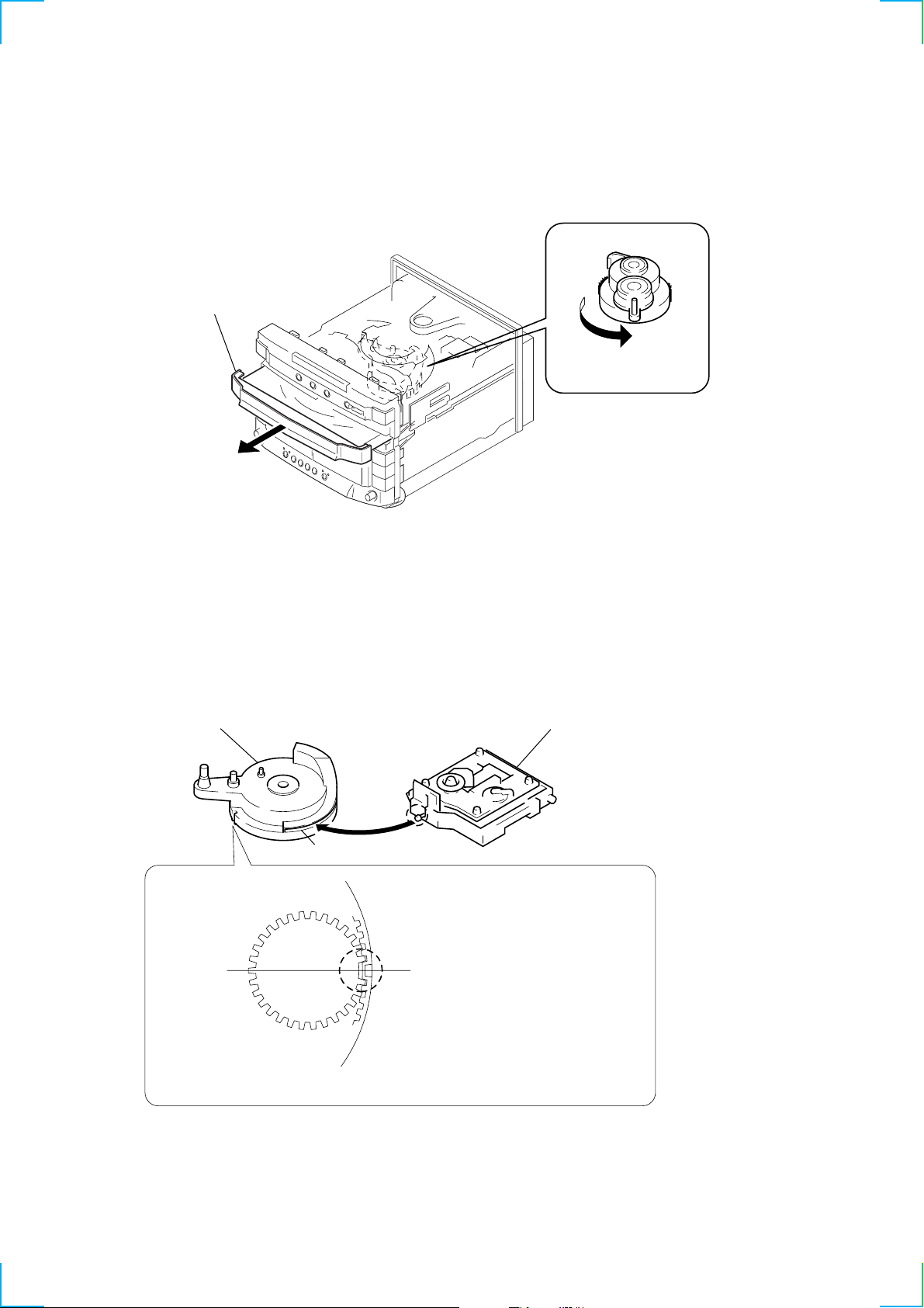
SERVICING NOTE
HOW TO OPEN THE DISC TRAY WHEN POWER SWITCH
TURNS OFF
1
Remove the Case.
3
Pull-out the disc tray.
2
Turn the cam to the
direction of arrow.
Note for Installation (ROTARY ENCODER)
BU cam
Groove
Note:When attaching the Base unit, Insert th
section A into the groove of BU cam.
Section A
Note:When attaching the BU cam,
engage the Rotary encoder
switch as shown in the figure.
4
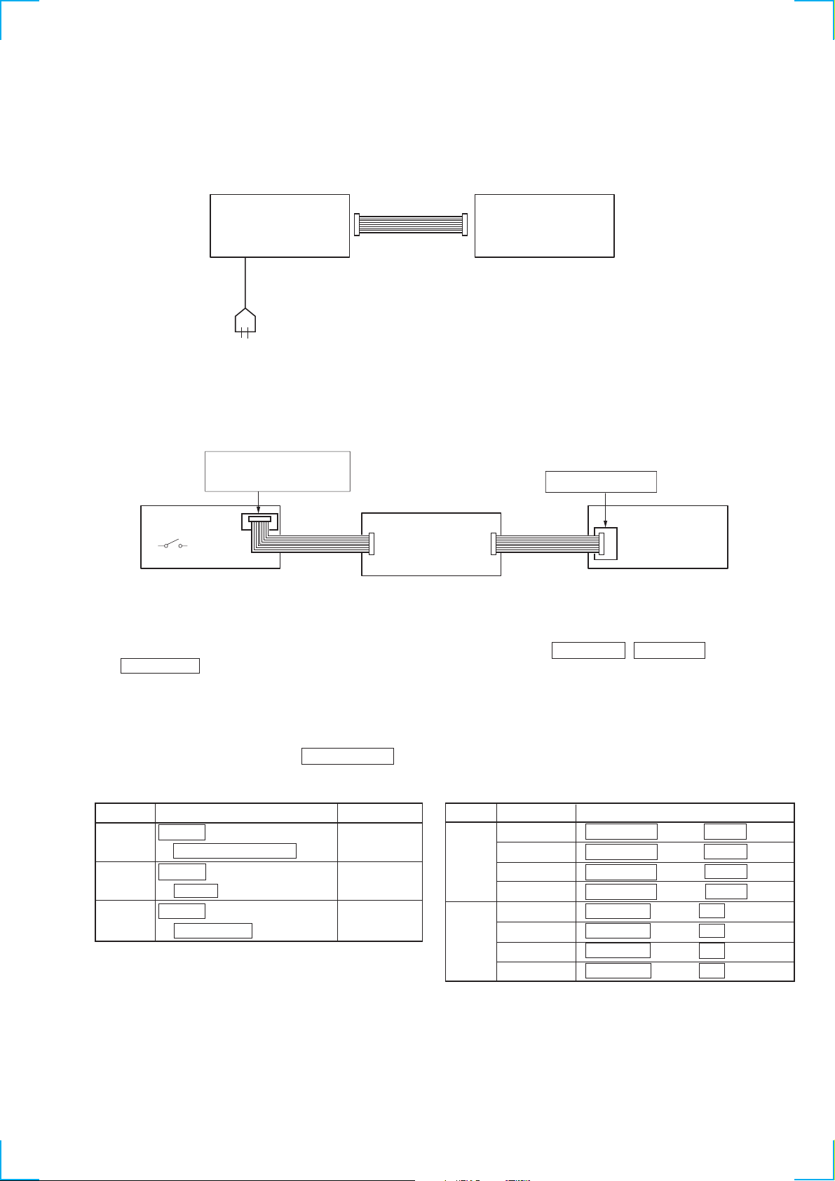
Connection and Operations of the Unit by Itself
This unit cannot be operated by itself as it does not come with a power supply.
Connect STR-VX500/VX700 as shown in “Connection 1” before beginning servicing.
Connection 1: If there is STR-VX500/VX700.
STR-VX500/VX700
SYSTEM CABLE 17P
AC IN
SET
Use a power supply jig (PFJ-1) if the STR-VX500/VX700 is not available.
Connect the conversion jig for connection (J-2501-138-A) as shown in “Connection 2” before beginning servicing.
Connection 2: If there is not STR-VX500/VX700.
FH-E939,838,737
MHC-6600,5600,3600,2600
CDP/TC
Power SW
Service Box (PFJ-1)
Conversion
Jig
(J-2501-138-A)
Connector
cable 17P
(Supplied with PFJ-1)
Conversion Jig or Set)
SYSTEM CONTROL
Set
Connector
cable 17P
(Supplied with
To operate the unit by itself, turn on the power of the conduction jig (PFJ-1), and press the s (TAPE A) , s (TAPE B) ,
and H (TAPE B) buttons together in this order.
As this unit is not equipped with fast forward and rewind buttons, buttons need to be combined and pressed together for different functions
when operating the unit by itself. (See Table-2.)
However, it will not operate properly if operations are performed without switching the functions.
Perform the following procedure to switch the functions before operating the unit.
The function selected is indicated by the DISC NUMBER indicator.
Table 1 Switching the Functions Table 2 Pressing Combination of Buttons When Operated by Itself
Function
CD x (CD) button 1< 2< 3
+ HI-SPEED DUBBING button
T APE A x (CD) button 1< 2 3
+ z REC button
TAPE B x (CD) button 1 2< 3
+ h (TAPE A) button
Operation
Indicator Deck Function
CD > (AMS) s (TAPE B) button + DISC3 button
. (AMS) s (TAPE B) button + DISC1 button
M s (TAPE A) button + DISC3 button
m s (TAPE A) button + DISC1 button
T APE A > (AMS) DISC SKIP button + H (TAPE B)
TAPE B . (AMS) DISC SKIP button + h (TAPE B)
Operation
M DISC SKIP button + H (TAPE A)
m DISC SKIP button + h (TAPE A)
The function can be differentiated by the lighting of this part of the indicator.
↓↓
1< 2< 3
5

Cold Reset
NOTE: This is the mode for operating the unit by itself. Take note that the operating method differs when connected to the STR-VX500/
VX700. This method is described in the manuals of the STR-VX500 and STR-VX700. Refer to these manuals for details.
This mode is used for initializing the RAM contents. Perform this mode when returning the repaired product to the customer.
Procedure:
1. After turning ON the power of the conduction jig (PFJ-1), press the s (TAPE A) button, s (TAPE B) button, and H (TAPE B)
button together in this order.
2. Press the X (TAPE) button while pressing the x (CD) button.
CD Delivery Mode
NOTE: This is the mode for operating the unit by itself. Take note that the operating method differs when connected to the STR-VX500/
VX700. This method is described in the manuals of the STR-VX500 and STR-VX700. Refer to these manuals for details.
This mode moves the pickup to areas where the anti-vibration is stronger. Perform this mode when returning the repaired product
to the customer.
Procedure:
1. After turning ON the power of the conduction jig (PFJ-1), press the s (TAPE A) button, s (TAPE B) button, and H (TAPE B)
button together in this order.
2. Press the CD SYNCHRO button while pressing the x (CD) button.
3. Wait untill z (TAPE B) indicator is on befor disconnect from the conduction jig (PFJ-1).
LED All Lit Mode
NOTE: Always perform this mode when operating the unit by itself.
This mode is used for lighting up the whole LED.
Procedure:
1. After turning ON the power of the conduction jig (PFJ-1), press the s (TAPE A) button, s (TAPE B) button, and H (TAPE B)
button together in this order.
2. The whole LED can be turned on and off each time the s (TAPE A) button is pressed while pressing the x (CD) button.
3. Press the three buttons in step 1 at the end.
Key Check Mode
NOTE: Always perform this mode when operating the unit by itself.
This mode is used for checking the key inputs of the buttons of the unit.
Procedure:
1. After turning ON the power of the conduction jig (PFJ-1), press the s (TAPE A) button, s (TAPE B) button, and H (TAPE B)
button together in this order.
2. Press the DOLBY NR button while pressing the x (CD) button to set the key check mode, and the indicator displays “3 HX”.
3. The number of buttons pressed are indicated in binary digits by the indicator LED. Buttons pressed once are not counted when pressed
again.
4. Press the two buttons in step 2 at the end.
Display: 1< 2< 3
MSB ↑
↑ LSB
Aging Mode
NOTE: Perform the following procedure only when operating the unit by itself.
This mode is used for checking the operations of the CD player and tape deck.
The operations are the same as the aging mode described in the service manual for the STR-VX500/VX700. However as this unit
does not have a fluorescent indicator tube, operating states and error statuses cannot be checked.
If the STR-VX500/VX700 is available, set the aging mode according to those service manuals.
Aging continues in the following sequence as long as no errors occur.
Aging of CD player (12 minutes)
Aging of deck A
Aging of deck B
12 minutes
Procedure:
1. After turning ON the power of the conduction jig (PFJ-1), press the s (TAPE A) button, s (TAPE B) button, and H (TAPE B)
button together in this order.
2. Press the s (TAPE B) button while pressing the x (CD) button to set the aging mode and start aging.
3. To end aging, press the three buttons in step 1.
6
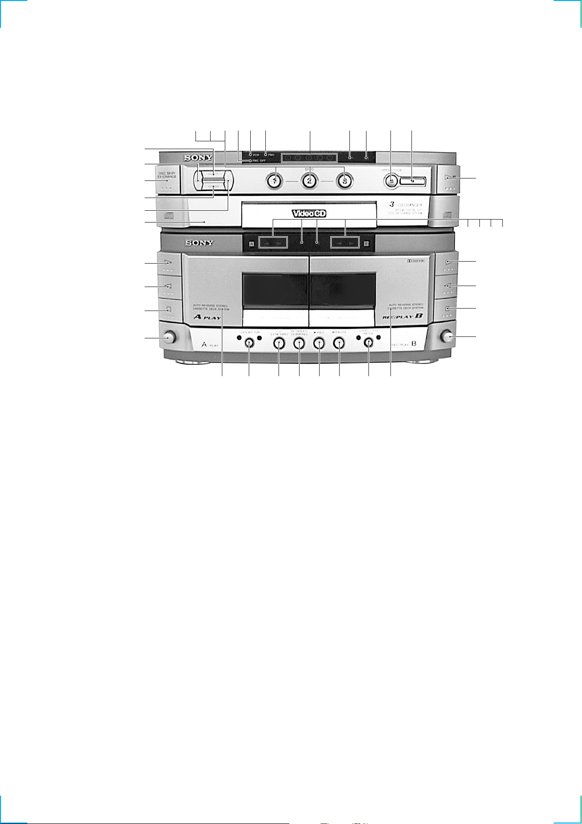
Front Panel
SECTION 2
GENERAL
ef
ed
1
es
eg
ea
e;
wl
wk
wj
234 5 6 7 8 9
ekejeh
wawswdwfwg qlwh
w;
0
qa qs qd qf
qg
qh
qj
qk
Location of Parts and Controls
1 DISC SKIP/EX-CHANGE button
2 DISC 1 button
3 DISC 2 button
4 DISC 3 button
5 DISC NUMBER 1< 2< 3 indicator
6 N (CD play) indicator
7 X (CD pause) indicator
8 A OPEN/CLOSE button
9 x (CD stop) button
0 HX (CD play pause) button
qa bB (Deck A play) indicator
qs z (Deck B rec) indicator
qd X (Tape (Deck B pause)) indicator
qf bB (Deck B play) indicator
qg H (Deck B play) button
qh h (Deck B play) button
qj s (Deck B stop) button
qk A (Deck B eject) button
ql Casette lid (Deck B)
w; DIRECTION MODE button
wa X PAUSE button
ws z REC button
wd HI-SPEED DUBBING button
wf CD SYNCHRO button
wg DOLBY NR button
wh Casette lid (Deck A)
wj A EJECT (Deck A) button
wk s (Deck A stop) button
wl h (Deck A play) button
e; H (Deck A play) button
ea Video CD Disc tray
es RETURN button
ed PREV button
ef SELECT button
eg NEXT button
eh PBC OFF indicator
ej VCD indicator
ek PBC indicator
7
SECTION 3
DISASSEMBLY
Note: Follow the disassembly procedure in the numerical order given.
3-1. LOADING PANEL
3
Loading panel
(Remove two claws)
Two claws
2
Pull-out the disc tray.
1
Turn the cam to the
direction of arrow.
3-2. BACK PANEL AND CD MECHANISM DECK
qf
CD mechanism deck
qs
Connector
(CN111)
0
Screw
(BVTP3
×
10)
qd
Connector
(CN112)
7
Back panel
4
Two screws
(BVTP3
×
10)
6
Four screws
(BVTP3
5
Three screws
(BVTP3
qa
Flat type wire
(19core, CNS103)
×
8)
1
Screw
(BVTP3
2
Cover (SC)
3
System cable
×
10)
×
8)
9
Dummy board
8
Two screws
(BVTP3
×
10)
8
3-3. FRONT PANEL
r
A
1
Three screws
(BVTP2.6 × 8)
2
Two screws
(BVTP2.6 × 8)
3
TC mechanism deck
4
Two springs
C
D
D
C
5
Remove the Cassette holder A
and Cassette holder B.
(Remove C first, and remove D.)
6
Eject button
A
7
Eject button
B
Note for installation
Set the Spring to be at the position
in the figure.
B
(Push out in the direction
of the arrow A.)
(Push out in the direction
of the arrow B.)
8
Front panel
(Remove the catcher)
3
Flat type wire
(15core, CNS101)
6
Lead (with connector)
2
Flat type wire
(17core, CNS104)
Catcher
1
Flat type wire
(17core, CNS102)
7
Connector (CNP105)
4
Connecto
(CN113)
3-4. TC MECHANISM DECK AND CASSETTE HOLDER
5
Two screws
(BVTP3
×
10)
9
3-5. DISC TRAY
4
Two claws
2
Pull-out the disc tray.
5
Remove the disc tray.
3
Flat type wire (8 core)
Note: When installing the Disc tray, pull around the flat type wire to
pass through the claw A and claw B , as shown in the figure.
Claw
Claw
A
B
1
Turn the cam the
direction of arrow.
10
SECTION 4
MECHANICAL ADJUSTMENTS
SECTION 5
ELECTRICAL ADJUSTMENTS
Precaution
1. Clean the following parts with a denatured alcohol-moistened
swab:
record/playback heads pinch rollers
erase head rubber belts
capstan idlers
2. Demagnetize the record/playback head with a head
demagnetizer.
3. Do not use a magnetized screwdriver for the adjustments.
4. After the adjustments, apply suitable locking compound to the
parts adjusted.
5. The adjustments should be performed with the rated power
supply voltage unless otherwise noted.
Torque Measurement
Mode
FWD
FWD
back tension
REV
REV
back tension
FF/REW
FWD tension
REV tension
Torque meter
CQ-102C
CQ-102C
CQ-102RC
CQ-102RC
CQ-201B
CQ-403A
CQ-403R
Meter reading
31 to 71 g • cm
(0.43 – 0.98 oz • inch)
2 to 6 g • cm
(0.02 – 0.08 oz • inch)
31 to 71 g • cm
(0.43 – 0.98 oz • inch)
2 to 6 g • cm
(0.02 – 0.08 oz • inch)
71 to 143 g • cm
(0.98 – 1.99 oz • inch)
100 g or more
(3.53 oz or more)
100 g or more
(3.53 oz or more)
Read before adjustments
T o adjust the unit, operate the unit by itself using the conduction jig
(PFJ-1).
For details on switching functions and fast forwarding the unit, etc.
when operating it by itself, refer to “Connection and Operations of
the Unit by Itself” on page 5 of Servicing Notes.
• Turning on the power
When operating the unit by itself:
1. After turning ON the power of the conduction tool (PFJ-1),
press the s (T APE A) button, s (TAPE B) button, and H
(TAPE B) button together in this order.
Inputting/outputting audio signals:
Use the jack of the power supply jig (PFJ-1).
Output point
Input point
PFJ-1
DECK SECTION 0 dB=0.775V
1. Demagnetize the record/playback head with a head
demagnetizer.
2. Do not use a magnetized screwdriver for the adjustments.
3. After the adjustments, apply suitable locking compound to the
parts adjusted.
4. The adjustments should be performed with the rated power
supply voltage unless otherwise noted.
5. The adjustments should be performed in the order given in this
service manual. (As a general rule, playback circuit adjustment
should be completed before performing recording circuit
adjustment.)
6. The adjustments should be performed for both L-CH and RCH.
7. Switches and controls should be set as follows unless otherwise
specified.
Tape
P-4-A100
WS-48B
P-4-L300
Signal
10 kHz, –10 dB
3 kHz, 0 dB
315 Hz, 0 dB
Used for
Azimuth Adjustment
Tape Speed Adjustment
Level Adjustment
Record/Playback Head Azimuth Adjustment
(Deck A, Deck B)
Note: Perform this adjustments for both decks.
Procedure:
1. Mode : Playback
test tape
P-4-A100
(10kHz, -10dB)
set
PFJ-1
level meter
output point
11
2. Turn the adjustment scre w and check output peaks. If the peaks
e
)
do not match for L-CH and R-CH, turn the adjustment screw
so that outputs match within 1 dB of peak.
L-CH
peak
screw
position
R-CH
peak
output
level
within
1 dB
L-CH
peak
R-CH
peak
within 1dB
screw
position
3. Mode: Playback
test tape
P-4-A100
(10kHz, -10dB)
output point
oscilloscop
Tape Speed Adjustment (Deck B)
Note: Set the test mode using the following method and begin tape
speed adjustment.
In the test mode, the speed will switch to double speed or
normal speed each time the HI-DUB button is pressed.
Procedure:
Press the x (CD) button while pressing the DIRECTION MODE
button.
1. Insert the WS-48B into deck B, while pressing the x (CD)
button, press the h (TAPE A) button, set the function to
“deck B”.
2. Press the H button of deck B.
3. Press the HI-DUB button and play the tape at double speed.
4. Adjust RV1001 of the LEAF SW board so that the reading of
the frequency counter becomes 6000 ± 180 Hz.
5. Press the HI-DUB button and play the tape at normal speed.
6. Adjust RV1002 of the LEAF SW board so that the reading of
the frequency counter becomes 3000 ± 90 Hz.
Adjustment Location: LEAF SW board
Sample Value of Wow and flutter
W.RMS (JIS) less than 0.3%
(test tape: WS-48B)
set PFJ-1
Waveform of oscilloscope
in phase 45
good
°
90
135
°
°
wrong
180
°
4. After the adjustments, apply suitable locking compound to the
parts adjusted.
Adjustment Location: Playback Head (Deck A)
Record/Playback/Erase Head (Deck B)
Playback Level Adjustment (Deck A, Deck B)
Procedure:
Mode: Playback
test tape
P-4-L300
(315Hz, 0dB)
set
PFJ-1
level meter
output point
Deck A is RV311 (L-CH) and RV411 (R-CH), deck B is RV301
(L-CH) and RV401 (R-CH)
so that adjustment within the following adjustment level.
Adjustment level:
Output point from PFJ-1 playback level: 301.5 to 338.3 mV (–8.2
to –7.2 dB)
level difference between the channels: within ± 0.5 dB
Adjustment Location: AUDIO board
Adjustment Location
[LEAF SW BOARD]
Reverse
Forward
12
RV1002 RV1001
RV1001(High Speed)
RV1002(Normal Speed
Record Bias Adjustment (Deck B)
e
Record Level Adjustment (Deck B)
Procedure:
1. Press the x (CD) button while pressing the DIRECTION
MODE button.
2. While pressing the x (CD) button, press the h (TAPE A)
button, set the function to “deck B”.
3. Insert a tape into deck B, press the z REC button, and then
press the N button to start recording.
4. Mode: Record
INPUT POINT
AF OSC
attenuator
1) 315 Hz
2) 10 kHz
600
Ω
PFJ-1
} 50 mV (–23.8 dB)
blank tap
CS-123
set
5. Mode: Playback
recorded
position
PFJ-1
set
level meter
output
point
6. Confirm playback the signal recorded in step 2 become
adjustment level as follows.
If these levels do not adjustment level, adjust the RV341 (LCH) and R V441 (R-CH) on the A UDIO board to repeat steps 3
and 4.
Adjustment level: The playback output of 10 kHz lev el dif ference
against 315 Hz reference should be ± 1.0 dB.
Procedure:
1. Press the x (CD) button while pressing the DIRECTION
MODE button.
2. While pressing the x (CD) button, press the h (T APE A)
button, set the function to “deck B”.
3. Insert a tape into deck B, press the z REC button, and then
press the N button to start recording.
4. Mode: Record
INPUT POINT
AF OSC
attenuator
315Hz 50 mV (–23.8 dB)
600
Ω
PFJ-1
set
blank tape
CS-123
5. Mode: Playback
recorded
position
PFJ-1
set
level meter
output
point
6. Confirm playback the signal recorded in step 2 become
adjustment level as follows.
If these levels do not adjustment level, adjust the RV301 (LCH) and R V351 (R-CH) on the MAIN board to repeat steps 3
and 4.
Adjustment level:
Output point from PFJ-1 playback level: 47.2 to 53.0 mV (–24.3 to
–23.3 dB)
Adjustment Location: AUDIO board
Adjustment Location
[AUDIO BOARD] (Conductor Side)
RV341(Lch),RV441(Rch)
Record Bias
RV301 RV401
RV441 RV341
RV301(Lch),RV401(Rch)
Playback Level (Deck B)
Adjustment Location: MAIN board
[MAIN BOARD] (Component Side)
RV311(Lch),RV411(Rch)
Playback Level (Deck A)
RV411
RV311
CNS102
CNS101
RV351
Record
Level (R ch)
RV301
Record
Level (L ch)
CNP105
13
CD SECTION
e
e
)
)
Notes:
1. CD block basically constructed to operate without adjustment. Therefore, check each item in order given.
2. Use YEDS-18 disc (Part No.: 3-702-101-01) unless otherwise indicated.
3. Use the oscilloscope with more than 10 MΩ impedance.
4. Clean an object lens by an applicator with neutral detergent when the
signal level is low than specified value with the following checks.
S-Curve Check
Connection:
oscilloscop
BD board
TP (FE)
TP (VC)
Procedure:
1. Connect the oscilloscope to TP (FE) and TP (VC) on BD board.
2. Connect between test point TP (FOK) and Ground by lead wire.
3. Turned power switch on.
4. Put disc (YEDS-18) in and turned power switch on again and
actuate the focus search. (actuate the focus search when disc
table is moving in and out.)
5. Confirm that the oscilloscope waveform (S-curve) is
symmetrical between A and B. And confirm peak to peak le vel
within 3.0 ± 1.0 Vp-p.
+
–
RF signal waveform
VOLT/DIV: 200 mV
TIME/DIV: 500 ns
(with the 10: 1 probe
in use)
level: 1.3 Vp-p
+0.25
–0.20
When observing the eye pattern, set the oscilloscope for AC range
and raise vertical sensitivity.
When a general remote commander is not used (1 Track Jump
Check):
Procedure:
1. Connect the oscilloscope to TP (TE) and TP (VC) on BD board.
2. Turned power switch on.
3. Put disc (YEDS-18) in and press the G button, and play the
number five track.
4. Press the G button. (Becomes the 1 track jump mode)
5. Confirm that the level B of the oscilloscope's waveform and
the A (DC voltage) of the center of the traverse waveform.
Confirm the following:
A – B
2 (A + B)
× 100 = ± 7 (%)
S-curve waveform
symmetry
A
within 3.0 ± 1.0 Vp-p
B
6. After check, remove the lead wire connected in step 2.
Note: • Try to measure several times to make sure that the ratio of A : B
or B : A is more than 10 : 7.
• Take sweep time as long as possible and light up the brightness
to obtain best waveform.
RF Level Check
Connection:
oscilloscop
(AC range)
BD board
TP (RF)
TP (VC)
+
–
Procedure:
1. Connect the oscilloscope to TP (RF) and TP (VC) on BD board.
2. Turned power switch on.
3. Put disc (YEDS-18) in and press the G button.
4. Confirm that the oscilloscope wav eform is clear and check RF
signal level is correct or not.
Note: Clear RF signal waveform means that the shape “≈” can be clearly
distinguished at the center of the waveform.
1 track jump waveform
0V
level: 1.3 ± 0.6 Vp-p
Connection Location:
[BD Board] (Side A)
CN101
TP
(FOK)
IC101
Center of the waveform
B
A (DC voltage
symmetry
CN102
IC103
TP
(TE)
TP
(FE)
TP (RF)
TP (VC
14
r
IC505
IC507
TP508
(27 MHz)
CT503
VIDEO
Frequency
Adjustment
SECTION 6
DIAGRAMS
HTC-VX500
VIDEO SECTION
Frequency Adjustment
Connection:
VIDEO board
TP508 (27 MHz)
Procedure:
1. Connect the frequency counter to TP508 (27 MHz) on VIDEO
board.
2. Turned power switch on.
3. Press the FUNCTION button to select the CD.
4. Adjust CT503 on the VIDEO board so that the frequency
counter reading 27.0 MHz ± 80 Hz at stop status.
Adjustment Location:
[VIDEO BOARD] (Side A)
frequency counte
+
–
6-1. CIRCUIT BOARDS LOCATION
CD PANEL board
TC LED board
TC (A) board
TC PANEL board
VIDEO board
REG board
VIDEO IN/OUT board
MAIN board
TC (B) board
MOTOR (TURN) board
CONNECTOR board
BD board
SENSOR board
LEAF SW board
MOTOR (SLIDE) board
AUDIO board
1515
HTC-VX500
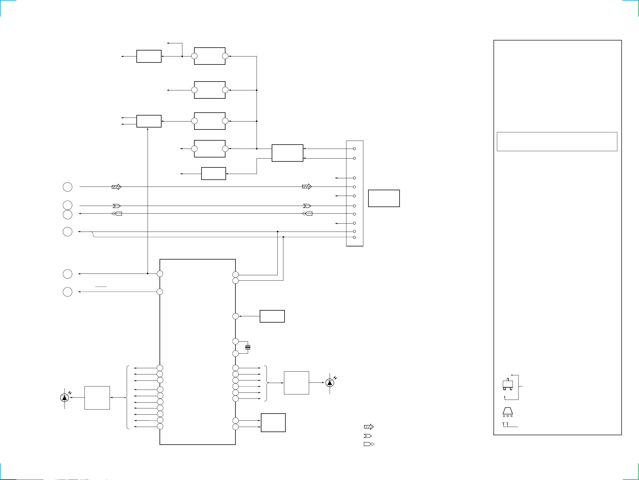
6-2. BLOCK DIAGRAMS
SERVO SECTION
DETECTOR
A
B
C
D
F
E
OPTICAL PICK-UP
(KSS-213BA/F-NP)
LASER DIODE
PD
2-AXIS
DEVICE
(TRACKING)
(FOCUS)
16
I-V AMP
10
LD
(SPINDLE)
7
4
2
1
5
6
M101
M102
(SLED)
A+5V
AUTOMATIC
M
M
A
3
B
4
C
5
D
6
F
F I-V AMP
8
E
9
E I-V AMP
POWER
CONTROL
Q101
FOCUS/TRACKING COIL DRIVE,
SPINDLE/SLED MOTOR DRIVE
OUT+
27
OUT–
26
OUT+
13
OUT–
12
OUT–
2
OUT+
1
OUT+
16
OUT–
17
RF AMP,
FOCUS/TRACKING ERROR AMP
1
MOTOR
LD
IC102
DRIVE
MOTOR
DRIVE
COIL
DRIVE
COIL
DRIVE
IC103
RF
SUMMING
AMP
APC LD
AMP
IN+
IN–
IN–
IN+
IN–
IN+
MUTE
FOCUS
ERROR AMP
TRACKING
ERROR AMP
APC PD
AMP
IN+, IN–
23, 24
9
10
4
5
19
20
15
RF EQ
AMP
RFO
RFE
FE BIAS
LDON
IC104
6320
FILTER
32
34
33
MDS
97
31
FILO
DIGITAL PLL
VARI-PITCH
DOUBLE SPEED
PROTECTOR
TIMING
GENERATOR 1
28
LDON
A+5V
PCO
SYNC
SCOR
74
18
S101
(LIMIT)
WFCK
73
SCOR
1
CLTV
SENSE
3
FILI
TIMING
GENERATOR 2
DSP LATCH
DSP CLK
DSP DATA
4
5
EFM
DEMODULATOR
SYSTEM CONTROLLER
IC101 (1/3)(MAIN BOARD)
ADDRESS
GENERATOR
SUBCODE Q
PROCESSOR
SUBQ
SQCK
77
78
37
36
SUBQ CLK
DISC-SENS
LOAD-OUT
REGISTER
32K
RAM
SUBQ DATA
CD MECHANISM
T-SENS
OPEN
ENC1
ENC2
ENC3
LOAD-IN
TBL-L
TBL-R
PRIORITY
ENCODER
SUBCODE P – W
PROCESSOR
EXCK
76
D+5V
CONTROLLER
IC502 (1/2)
75
76
81
80
79
78
63
64
60
61
DIGITAL SIGNAL PROCESSOR
IC101 (1/2)(BD BOARD)
COUT
89
RFAC
36
ASYI
38
ASYO
39
NOISE
SHAPER
DIGITAL SERVO
PROCESSOR
IC101 (2/2)
(BD BOARD)
MIRR/DFCT/
FOK
DETECTOR
SERVO AUTO
SEQUENCER
CPU
INTERFACE
ASYMMETRY
CORRECTOR
OVERSAMPLING
PROCESSOR
FSW
94
FOK
MIRR
DFCT
SENS
DATA
CLOK
XLAT
SSTP
MIX
18-TIMES
FILTER
CLV
MDP
MON
95
96
93
91
92
80
86
88
87
99
16
RF EQ
SWITCH
17
Q102, 103
FE
15
14
TE
13
19
PD
2
SFDR
100
SRDR
2
TFDR
4
TRDR
6
FFDR
8
FRDR
10
CTL1
CTL2
26
29
28
27
FE
TE
SE
RFDC
A/D
CONVERTER
PWM GENERATOR
FOCUS/TRACKING/SLED
SERVO DSP
FOCUS/TRACKING/SLED
SERVO
INTERFACE
62
XTAI
VCKI
XTAO
CLOCK
GENERATOR
INTERNAL BUS
SBSO
75
ERROR
CORRECTOR
PEAK
DETECTOR
DIGITAL
OUT
SCLK
83
2
SENSE CLK
LEVEL SHIFT
Q701
(OPEN/CLOSE DET)
4
ROTARY
2
ENCODER
S811
3
DISC TRAY SLIDE MOTOR DRIVE
10
DISC TRAY TURN MOTOR DRIVE
IC801
FIN
MOTOR
RIN
DRIVE
2
IC701
IN1
3
MOTOR
IN2
DRIVE
6
D/A DIGITAL
PROCESSOR
MUTE
79
10
DSP MUTE
DISC SENSOR
IC703
TABLE SENSOR
IC702
S801
CLOSE
OPEN
OUT1
OUT2
OUT1
OUT2
PROCESSOR
SERIAL/PARALLEL
CTRL1
CTRL2
7
M
4
7
M
2
XTSL
64
DATA
46
BCLK
47
LRCK
45
GFS
54
RFCK
55
C2PO
56
DOUT
71
81
XRST
11
27
M801
(SLIDE MOTOR)
M701
(TURN MOTOR)
CTL1
DATA
BCK
LRCK
C2PO
TRANSCEIVER
CTL1
CTL2
MCLK
33.8MHz
DATA, BCK,
LRCK, C2PO
OPTICAL
IC107
• SIGNAL PATH
: CD PLAY
: DIGITAL OUT
(Page 17)
A
(Page 17)
B
CD OPTICAL
DIGITAL OUT
RESET
C
(Page 17)
1616
AUDIO/VIDEO CD SECTION
DATA,
BCK,
LRCK,
DATA
C2PO
B
(Page 16)
BCK
LRCK
C2PO
LEVEL
SHIFT
IC501
MPEG VIDEO/AUDIO DECODER,
VIDEO SIGNAL PROCESSOR
IC505
CD-DATA
4
CD-BCK
3
CD-LRCK
5
CD-C2PO
6
ADDRESS BUS
CD-ROM
INTERFACE
CIRCUIT
MA0 – MA10
58 – 56, 54, 52 – 50, 48, 46 – 44 10 – 15, 17, 19, 21, 23 – 29
A0 – A10
MPEG
SYSTEM
DECODER
D-RAM/ROM INTERFACE
MD0 – MD15
MPEG
AUDIO
DECODER
MPEG
VIDEO
DECODER
D0 – D15
MCE
37
VIDEO
PROCESS
CIRCUIT
RAS0
MWE
38 42 40
AUDIO
INTERFACE
CIRCUIT
CAS
60
RESET
DA-DATA
DA-BCK
DA-LRCK
DA-XCLK
Y-OUT
C-OUT
VCK-IN
PGIO2/VSYNC/CSYNC
CPU INTERFACE
HRDY
HSEL
HD-OUT
HD-IN
HINT
113
114 121
112
119
HTC-VX500
(Page 16)
XT1
DIGITAL FILTER,
D/A CONVERTER
DIGITAL
FILTER,
NOISE
SHAPER
CIRCUIT
IC509
D/A
CONVERTER
MODE
CONTROL
MC
MD
9 724 1
8
(Page 19)
VOUTL
LOW-PASS
FILTER
ML
RSTB
10
VOUTR
14
11
LOW-PASS
FILTER
IC101
R-CH
• SIGNAL PATH
CD-L
E
: CD PLAY (AUDIO)
: CD PLAY (VIDEO)
A
MCLK
33.8MHz
110
111
108
86
69
75
106
93
HCK
117
BUFFER
Q502
DATA
CLK
OSC
BUFFER
IC504
DATA
18
BCK
17
LRCK
19
768FSO
21
384FSO
20
MCKO
4
INPUT
INTERFACE
CIRCUIT
TIMING CONTROL/
CLOCK GENERATOR
XT2
X503
27MHz
D-RAM
IC507
(Page 19)
D
F
(Page 19)
A0 – A8
16 – 19, 22 – 26
A0 – A8
RESET
IIC-DATA, IIC-CLK
UCAS
LCAS
14 132928
DQ1 – DQ16
RAS
WE
D0 – D15
DATA BUS
A0 – A10
12 – 5, 27, 26, 23
A0 – A10
PROGRAM ROM
IC506
X401
8MHz
BUS
45
D0 – D7
13 – 15, 17 – 212 – 5, 7 – 10, 31 – 34, 36 – 39
O0 – O7
XIN
19
XOUT
20
12C.DATA
14 13
IIC-DATA
12C.CLK
IIC-CLK
D8 – D14
25, 4, 28, 29, 3, 2, 30
A11 – A17
22
EXPANSION
IC402
RESET
CLK1
33
DATA1O
31
32
DATA1I
CL680 SEL
D502
21
20
CL680 HINT
CL680 HRDY
23
24
CL680 RESET
CD MECHANISM CONTROLLER
93
NT/PAL
TEST LED
73
72
UTOI
19
ITOU
29
RXD
30
TXD
12
XRESET
29
CLK
DATA
30
CE
S501
SYSTEM SELECT
NTSC
AUTO
PAL
RXD
UTAU
TXD
UTAI
10918
1112
(SELF DIAGNOSIS)
IIC-DATA
IIC-CLK
DEVICE RESET
IC502 (2/2)
DF LATCH
SHARPNESS
VMUTE
22
77
VIDEO
BUFFER
Q303
13
VIDEO AMP
IC401 (1/2)
B.P.F.
B.P.F.
34
65
VIDEO
BUFFER
Q301
VIDEO
BUFFER
Q304
SHARPNESS
CONTROL SWITCH
Q306
SHARPNESS
FILTER
Q302
VIDEO
BUFFER
Q307
VIDEO
BUFFER
Q308
Y/C MIX
Q310
5
VIDEO AMP
IC401 (2/2)
VIDEO
MUTE
Q453
7
VIDEO
MUTE
Q454
VIDEO SELECT
IC601
1
3
2
C
Y
VIDEO
BUFFER
7
Q601
RESET
CD POWER
(Page 16)
3
4
(Page 19)
1
2
C
J301
S VIDEO OUT
J601
VIDEO IN
MONITOR OUT
J
XOUT
XIN
1315
16
X501
10MHz
1717
HTC-VX500
TAPE DECK SECTION
HP101
(PLAYBACK)
L-CH
R-CH R-CH
HRPE101 (1/2)
(RECORD/PLAYBACK)
L-CH
R-CH R-CH
DECK PROCESS
DECK A/B SELECT, PB/REC EQ AMP,
DOLBY NR AMP, ALC, AMS
IC301
DOLBY PASS
NORM/HIGH
PB A/B
70
120
R-CH
NR ON/OFF
BIAS ON/OFF
RM ON/OFF
+
L.P.F.
BUFFER
28
27
AMS
CIRCUIT
REC/PB/PASS
LM ON/OFF
26
MAOUT
MSIN
MSOUT
RIN (L)
43
ALC (L)
44
DOLBY NR
ALC
ALC
ROUT (L)
35 34
AMP
CIRCUIT
IN (L)
REC OUT (L)
39
RV301
REC LEVEL (L)
(DECK B)
EQ IN (L)
38
PB EQ AMP
(DECK A)
IC611
RV311
PB LEVEL (L)
(DECK A)
PB EQ AMP
(DECK B)
IC601
REC/PB SWITCHING
3
1
R-CH
IC602
R-CH
RV301
PB LEVEL (L)
(DECK B)
4
AIN (L)
48
BIN (L)
46
BIAS (N)
33
BIAS (C)
32
BIAS (M)
31
S1004
(DECK A 120/70)
S1008
(DECK B 120/70)
BIAS
CONTROL
CIRCUIT
B NORM/CROM
ALC ON/OFF
A 120/70
1516182022 23242517
19
REC
EQ AMP
PB OUT (L)
EQ OUT
40
(L)
36
PB-L
REC-L
G
(Page 19)
H
(Page 19)
• SIGNAL PATH
: PB (DECK A)
: PB (DECK B)
: REC
HRPE101 (2/2)
(ERASE)
16
RV441
REC BIAS (R)
(DECK B)
R-CH
2
RV341
REC BIAS (L)
(DECK B)
BIAS OSC
T621
BIAS OSC
Q621, 622
REC BIAS
SWITCH
Q623
C331, L331
BIAS
TRAP
B+
(A+7V)
97
TC-RELAY
A-PLAY-SW
95 96
S1001
(A PLAY)
9994939290 898887
BIAS
PB-A/B
EQ-H/N
ALC-ON/OFF
B-PLAY-SW
S1002
(B PLAY)
R/P-PASS
REC-MUTE
NR-ON/OFF
S1003
(A HALF)
TC-MUTE
31
98
AMS-IN
A-HALF
ROTATION
DETECT SENSOR
(DECK A)
IC1001
26
S1006
(B HALF)
S1009
(REC B)
A-SHUT
B-HALF
28
ROTATION
DETECT SENSOR
(DECK B)
IC1002
27
B-SHUT
S1005
(REC A)
SL1
TRIGGER PLUNGER
DECK A
TRIGGER
PLUNGER DRIVE
(DECK A)
Q333, 334
84
SYSTEM CONTROLLER
IC101 (2/3)
A-TRG
SL2
TRIGGER PLUNGER
DECK B
TRIGGER
PLUNGER DRIVE
(DECK B)
Q331, 332
83
B-TRG
Q335
RV1001
TAPE SPEED
(HIGH)
82
CAPM-ON/OFF(+)
CAPM-EMG(+)
CAP-M-H/L
CAPM-EMG(–)
CAPM-ON/OFF(–)
CAPSTAN MOTOR
CONTROL SWITCH
Q1001
100
1
85
86
MOTOR DRIVE
MOTOR DRIVE
RV1002
TAPE SPEED
(NORMAL)
CAPSTAN
Q336 – 339
CAPSTAN
Q340 – 343
M
M1
(CAPSTAN)
1818
POWER SECTION
d
(Page 17)
(Page 18)
(Page 18)
(Page 17)
(Page 17)
(Page 17)
16
E
G
H
F
J
D
D224-230
CD-L
PB L
REC L
IIC-DATA
IIC-CLK
CD-POWER
RESET
LED
ON/OFF
SWITCH
Q214-223
A+7.5V
D+5V
A+5V
+7.5V REG
Q852
+5V SW
Q102-104
M12V
+5V
46
57
52
66
65
67
72
54
70
69
53
68
M+7V
A-7.5V
CD-POWER
XRST
MASTER CONTROL
DECO1
DECO2
CD-PAUSE
CD-PLAY
DISC1
DISC2
DISC3
EXIST1
EXIST2
EXIST3
+12V REG
3 1
IC851
+5V REG
3 1
IC852
+5V REG
3 1
IC854
+7V REG
3
IC853
-7.5V REG
Q855
IIC DATA
IC101
LED1
LED2
LED3
LED4
LED5
LED6
KEY A
KEY B
1
IIC CLK
RESET
HTC-VX500
THIS NOTE IS COMMON FOR PRINTED WIRING
BOARDS AND SCHEMATIC DIAGRAMS.
(In addition to this, the necessary note is printed
in each block.)
For schematic diagrams.
Note:
• All capacitors are in µF unless otherwise noted. pF: µµF
50 WV or less are not indicated except for electrolytics
and tantalums.
• All resistors are in Ω and 1/
specified.
¢
•
: internal component.
• 1 : fusible resistor.
• C : panel designation.
Note: The components identified by mark ! or dotted line
+
-
RECT
D901-904
17
13
with mark ! are critical for safety.
Replace only with part number specified.
• U : B+ Line.
• V : B– Line.
(CD R)
R CH
(PB R)
R CH
(REC R)
R CH
3
2
9
7
6
4
14
16
CNB108
SYSTEM
CONTROL
• H : adjustment for repair.
• Voltages and waveforms are dc with respect to ground
under no-signal (detuned) conditions.
• Voltages are taken with a VOM (Input impedance 10 MΩ).
Voltage variations may be noted due to normal production tolerances.
• Waveforms are taken with a oscilloscope.
Voltage variations may be noted due to normal production tolerances.
• Circled numbers refer to waveforms.
• Signal path.
F : FM
f : AM
E : PB (DECK A)
d : PB (DECK B)
G : REC (DECK B)
J : CD (AUDIO)
L : CD (VIDEO)
c : DIGITAL OUT
55
56
For printed wiring boards.
Note:
• X : parts extracted from the component side.
• p : parts mounted on the conductor side.
®
•
: Through hole.
• b : Pattern from the side which enables seeing.
15
RESET
IC101
(The other layers' patterns are not indicated.)
• Abbreviation
HK : Hong Kong model
SP : Singapore model
X1
11
10
X2
2
3
4
5
6
7
X101
5MHz
D201-206
LED
ON/OFF
SWITCH
Q201-206
MY : Malaysia model
EA : Saudi Arabia model
TH : Thai model
IA : Indonesia model
• Indication of transistor
C
Q
These are omitted
EB
• R CH: Same as L ch
29
30
KEY
MATRIX
• SIGNAL PATH
: CD
C
EB
These are omitte
: PB
: REC
4
W or less unless otherwise
1919
HTC-VX500
6-3. PRINTED WIRING BOARD CD SECTION
• Refer to page 15 for Circuit Boards Location.
16
• Semiconductor
Location
Ref. No. Location
IC101 E-4
IC102 C-10
IC103 E-2
IC104 F-9
Q101 E-12
Q102 C-2
Q103 C-2
F
BA
(Page 32)
2020
 Loading...