

Sony HTC-NX300 Service manual
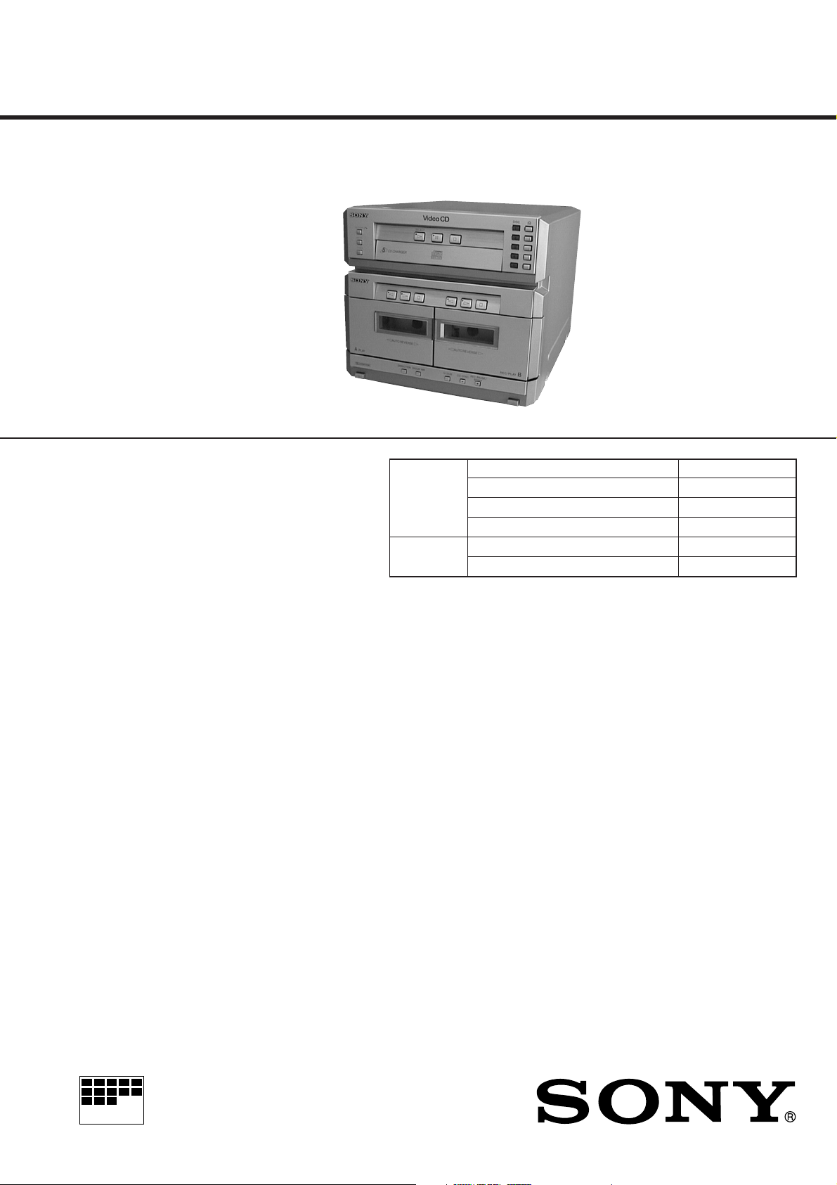
HTC-NX300
SERVICE MANUAL
HTC-NX300 is the CD player and Tape
Deck section in MHC-NX300AV.
Dolby noise reduction manufactured under license
from Dolby Laboratories Licensing Corporation.
“DOLBY” and the double-D symbol ; are trademarks of Dolby Laboratories Licensing Corporation.
CD
Section
Tape Deck
Section
E Model
Chinese Model
Model Name Using Similar Mechanism NEW
CD Mechanism Type CDM53E-K3BD37
Base Unit Name Type BU-K3BD37
Optical Pick-up Name KSM-213BFNV/Z-NP
Model Name Using Similar Mechanism HCD-GRX7
Tape Transport Mechanism Type TCM-230AWR2
SPECIFICATIONS
CD player section
System Compact disc and digital
Laser Semiconductor laser
Laser output Max. 44.6
Wavelength 780 – 790 nm
Frequency response 20 Hz – 20 kHz (±0.5 dB)
Signal-to-noise ratio More than 90 dB
Dynamic range More than 90 dB
Video color system format
CD DIGITAL OUT
(Square optical connector jack, rear panel)
Wavelength 660 nm
Output Level –18 dBm
audio system
(λ=780nm)
Emission duration:
continuous
*This output is the value
measured at a distance of
200 mm from the
objective lens surface on
the Optical Pick-up Block
with 7 mm aperture.
NTSC, PAL
µ
W*
Tape player section
Recording system 4-track
Frequency response 40 – 13,000 Hz (±3 dB),
(DOLBY NR OFF) using Sony TYPE I
General
Dimensions (w/h/d) Applox. 225 x 202 x 347
Mass Applox. 4.6 kg
Design and specifications are subject to change
without notice.
2-channel stereo
cassette
40 – 14,000 Hz (±3 dB),
using Sony TYPE II
cassette
mm
MICROFILM
MINI Hi-Fi COMPONENT SYSTEM

TABLE OF CONTENTS
1. SERVICING NOTES............................................... 3
2. GENERAL
Location of Controls ....................................................... 6
3. DISASSEMBLY ......................................................... 7
4. TEST MODE.............................................................. 14
5. MECHANICAL ADJUSTMENTS....................... 15
6. ELECTRICAL ADJUSTMENTS
TAPE DECK Section ...................................................... 15
CD Section ...................................................................... 18
VIDEO Section ............................................................... 19
7. DIAGRAMS
7-1. Block Diagram – SERVO Section – .............................. 21
7-2. Block Diagram – AUDIO/VIDEO CD Section –.......... 22
7-3. Block Diagram – TAPE DECK Section – ..................... 23
7-4. Block Diagram – POWER SUPPLY Section – ............. 24
7-5. Note for Printed Wiring Boards and
Schematic Diagrams ....................................................... 25
7-6. Printed Wiring Board – BD Board – ............................. 26
7-7. Schematic Diagram – BD Board – ................................ 27
7-8. Schematic Diagram – VIDEO Board (1/2) – ................ 28
7-9. Schematic Diagram – VIDEO Board (2/2) – ................ 29
7-10. Printed Wiring Board – VIDEO Board –....................... 30
7-11. Printed Wiring Boards
– CD MOTOR/SENSOR Section – ................................ 32
7-12. Schematic Diagram
– CD MOTOR/SENSOR Section – ................................ 33
7-13. Printed Wiring Board – AUDIO Board – ...................... 34
7-14. Schematic Diagram – AUDIO Board – ......................... 35
7-15. Printed Wiring Board – LEAF SW Board –.................. 36
7-16. Schematic Diagram – LEAF SW Board –..................... 36
7-17. Printed Wiring Board – MAIN Board – ........................ 37
7-18. Schematic Diagram – MAIN Board (1/2) – .................. 38
7-19. Schematic Diagram – MAIN Board (2/2) – .................. 39
7-20. Printed Wiring Board – POWER Board – ..................... 40
7-21. Schematic Diagram – POWER Board –........................ 41
7-22. Printed Wiring Boards – PANEL Section – .................. 42
7-23. Schematic Diagram – PANEL Section –....................... 43
7-24. IC Pin Function Description ........................................... 48
8. EXPLODED VIEWS ................................................ 57
9. ELECTRICAL PARTS LIST ............................... 64
SAFETY-RELATED COMPONENT WARNING!!
COMPONENTS IDENTIFIED BY MARK 0 OR DOTTED
LINE WITH MARK 0 ON THE SCHEMATIC DIAGRAMS
AND IN THE PARTS LIST ARE CRITICAL TO SAFE
OPERATION. REPLACE THESE COMPONENTS WITH
SONY PARTS WHOSE PART NUMBERS APPEAR AS
SHOWN IN THIS MANU AL OR IN SUPPLEMENTS PUBLISHED BY SONY.
2
SECTION 1
3
SERVICING NOTES
SELF-DIAGNOSIS
This unit is equipped with a self-diagnosis function.
The function is used for diagnosing the conditions of the circuits
of the VIDEO board.
The circuits can be determined if normal or abnormal by the lighting of D502 of the VIDEO board.
Lighting of D502
When lit : Operates normally
Blinks repeatedly: The circuit may be faulty.
[VIDEO Board] (Side B)
CN501
IC505
SL501
SL502
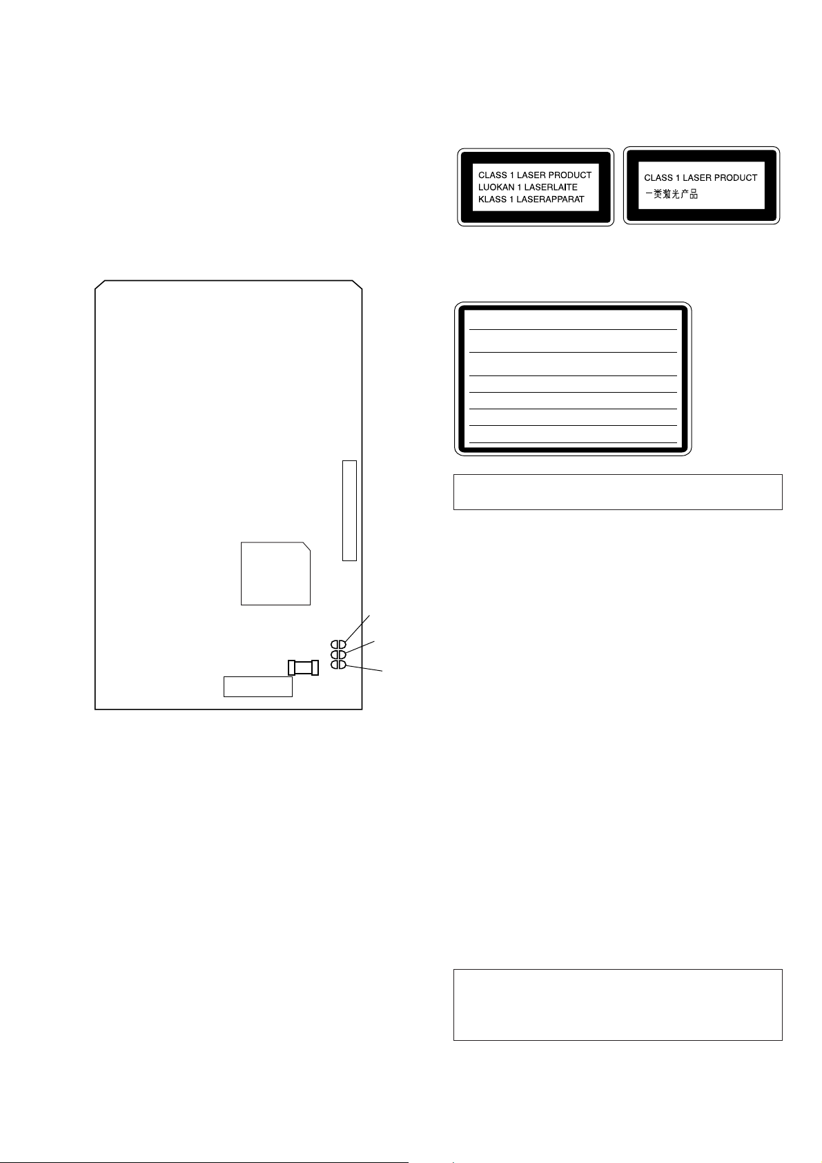
This appliance is classified as a CLASS 1 LASER product.
The CLASS 1 LASER PRODUCT MARKING is located on
the rear exterior.
Laser component in this product is capable of emitting radiation
exceeding the limit for Class 1.
The following caution label is located inside the unit.
CAUTION : INVISIBLE LASER RADIATION WHEN OPEN AND
INTERLOCKS DEFEATED. AVOID EXPOSURE TO BEAM.
ADVARSEL : USYNLIG LASERSTRÅLING VED ÅBNING NÅR
SIKKERHEDSAFBRYDERE ER UDE AF FUNKTION. UNDGÅ UDSAETTELSE
FOR STRÅLING.
VORSICHT : UNSICHTBARE LASERSTRAHLUNG, WENN
ABDECKUNG GEÖFFNET UND SICHEREITSVERRIEGELUNG
ÜBERBRÜCKT. NICHT DEM STRAHL AUSSETZEN.
VARO!: AVATT AESSA JA SUOJ ALUKITUS OHITETTAESSA OLET ALT-
TIINA NÄKYMÄTTÖMÄLLE LASERSÄTEILYLLE. ÄLÄ KATSO SÄTEESEEN.
VARNING : OSYNLING LASERSTRÅLING NÄR DENNA DEL ÄR ÖPPNAD
OCH SPÄRREN ÄR URKOPPLAD. BETRAKTA EJ STRÅLEN.
ADVERSEL : USYNLIG LASERSTRÅLING NÅR DEKSEL ÅPNES OG
SIKKERHEDSLÅS BRYTES. UNNGÅ EKSPONERING FOR STRÅLEN.
VIGYAZAT!: A BURKOLAT NYITÁSAKOR LÁTHATATLAN LÉZERSU-
!
KERÜLJE A BESUGÁRZÁST!
GÁRVESZÉLY
NOTES ON HANDLING THE OPTICAL PICK-UP
BLOCK OR BASE UNIT
The laser diode in the optical pick-up block may suffer electrostatic break-down because of the potential difference generated
by the charged electrostatic load, etc. on clothing and the human
body.
During repair, pay attention to electrostatic break-down and also
use the procedure in the printed matter which is included in the
repair parts.
The flexible board is easily damaged and should be handled with
care.
CN502
D502
SL50
NOTES ON LASER DIODE EMISSION CHECK
The laser beam on this model is concentrated so as to be focused
on the disc reflective surface by the objective lens in the optical
pick-up block. Therefore, when checking the laser diode emission, observe from more than 30 cm away from the objective lens.
Flexible Circuit Board Repairing
• Keep the temperature of the soldering iron around 270 ˚C during repairing.
• Do not touch the soldering iron on the same conductor of the
circuit board (within 3 times).
• Be careful not to apply force on the conductor when soldering
or unsoldering.
Notes on chip component replacement
• Never reuse a disconnected chip component.
• Notice that the minus side of a tantalum capacitor may be damaged by heat.
CAUTION
Use of controls or adjustments or performance of procedures
other than those specified herein may result in hazardous radiation exposure.
3
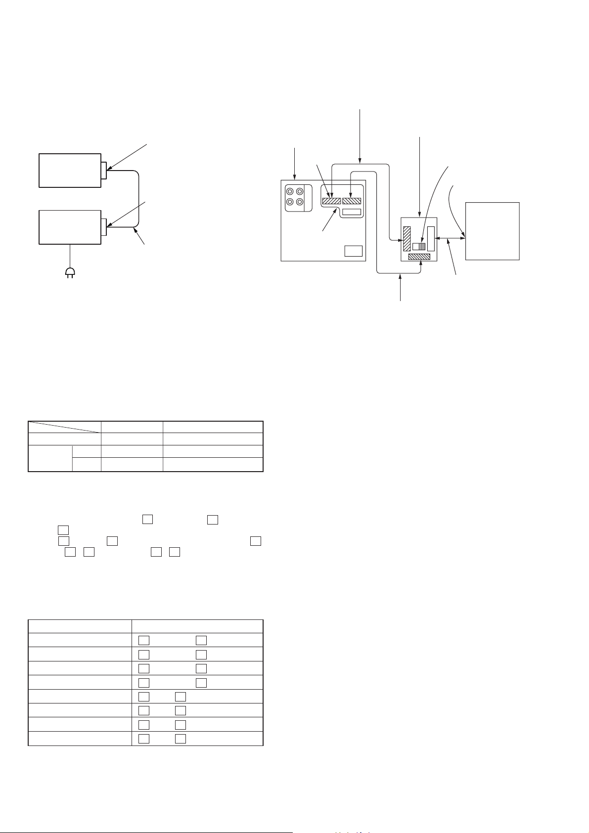
POWER SUPPLY DURING SERVICING
l
Connection:
• As this set has not own power supply, it does not operate independently. Therefore, during servicing, connect it to the PreMain amplifier and Tuner Unit (STR-NX300) of MHCNX300AV.
SYSTEM CONTROL termina
Set
SYSTEM CONTROL terminal
Pre-Main AMP
and T uner Unit
Connector cable (19P)
AC IN
If STR-NX300 are not available, use the Power Feed Jig (PFJ-
1) and Relay Connector Jig.
In this case, after turn on the POWER switch on the Power Feed
Jig, supply power with the following methods.
[Note]
The Power Feed Jig (PFJ-1) is deficient in power to drive this
set.
The details are listed below. For the items with × marking, use
the STR-NX300.
Connector cable (17P) of
attachment to power feed jig
Power feed jig
(PFJ-1)
CDP/TC
P707, P909
Relay connector jig
(J-2501-174-A)
ST
Exclusive cable (15P)
CD/TC signal
change switch
CN101 (19P)
SYSTEM CONTROL
terminal
Set
system cable
Operation check Characteristic measurement
Tape Deck af*1
CD section
CD a ×
SVCD ××
*1: Possible when a flat cable between CN111 (MAIN board) and
CN502 (VIDEO board) is disconnected.
Procedure:
1. Press three buttons of s (DECK B), A (DISC 1),
and s (CD) simultaneously.
2. The G (CD) and S (CD) LEDs blink, and then pressing G
(CD), G / g (DECK A), or G / g (DECK B) button can
make each play possible.
3. Also, the other functions are enabled by pressing two buttons
simultaneously.
A combination of respective functions and buttons is as follows.
function button
CD AMS – s (DECK A), S (CD)
AMS + s (DECK A), s (CD)
FR s (DECK B), S (CD)
FF s (DECK B), s (CD)
Deck-A REW/AMS – s (CD), g (DECK A)
FF/AMS + s (CD), G (DECK A)
Deck-B REW/AMS – s (CD), g (DECK B)
FF/AMS +
s (CD), G (DECK B)
4
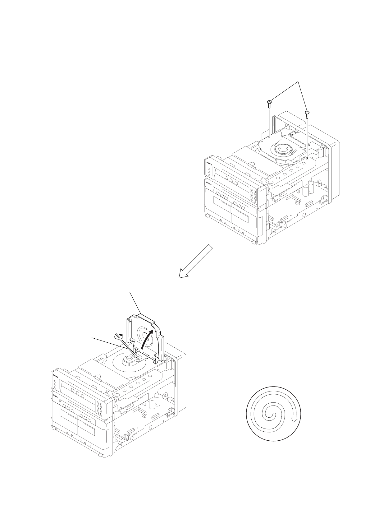
OPTICAL PICK-UP CLEANING
(Figure A)
2
four screws
(BVTP M2.6)
1
Remove the case. (Refer to disassembly page 7)
4
Cleaning the
optical pick-up.
3
Open the magnet
ass’y.
Note 1: In cleaning the lens, do not apply an excessive force.
As the optical pick-up is vulnerable, application of
excessive force could damage the lens holder.
Note 2: In cleaning, do not use a cleaner other than exclusive clean-
ing liquid (KK-91 or isopropyl alcohol).
Note 3: Wipe the objective lens spirally from center toward outside .
(See Figure A)
5
• LOCATION OF CONTROLS
– Front Panel –
123 45
6
H
S
7
8
9
hH s
0
qa
s
hH s
qhqgqfqdqs
SECTION 2
GENERAL
1 G (CD) button and indicator
2 S (CD) button and indicator
3 s (CD) button
A
1
2
3
4
5
ql
w;
wa
AA
qkqj
4 DISC1 to 5 buttons and indicators
5 A (DISC1 to 5) buttons and indicators
6 RETURN button
7 NEXT button
8 PREV button
9 g (DECK A) button and indicator
0 G (DECK A) button and indicator
qa s (DECK A) button
qs A (DECK A) button
qd DIRECTION button
qf DOLBY NR button
qg HI DUB button
qh CD SYNC button and indicator
qj REC PAUSE/START button and indicator
qk A (DECK B) button
ql s (DECK B) button
w; G (DECK B) button and indicator
wa g (DECK B) button and indicator
– Rear Panel –
1
1 SYSTEM SELECT switch
2 S VIDEO OUT jack
3 SYSTEM CONTROL connector
4 CD DIGTAL OUT OPTICAL terminal
5 VIDEO OUT jack
5
324
6
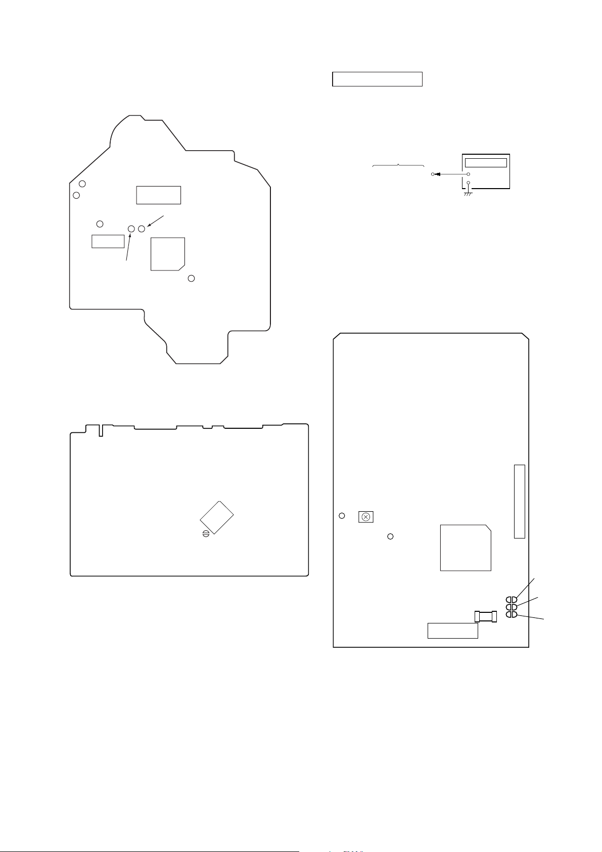
SECTION 3
r
DISASSEMBLY
Note: Follow the disassembly procedure in the numerical order given.
CASE
2
two screws
(case 3 TP2)
A
1
screw
(BVTP3
×
10)
3
Remove the case
in the arrow
direction.
2
two screws
(case 3 TP2)
A
FRONT PANEL SECTION
4
3
screw (BVTP3 × 5)
1
flat cable (15 core)
(CNS101)
8
front panel
section
harness
6
two screws
(BVTP3
1
flat cable (17 core)
(16 cm) (CNS104)
5
two screws
(BVTP3
×
10)
2
connector
(CN106)
2
connecto
(CN105)
7
claw
5
two screws
(BVTP3
×
5)
×
5)
1
flat cable (21 core)
(CN102)
7
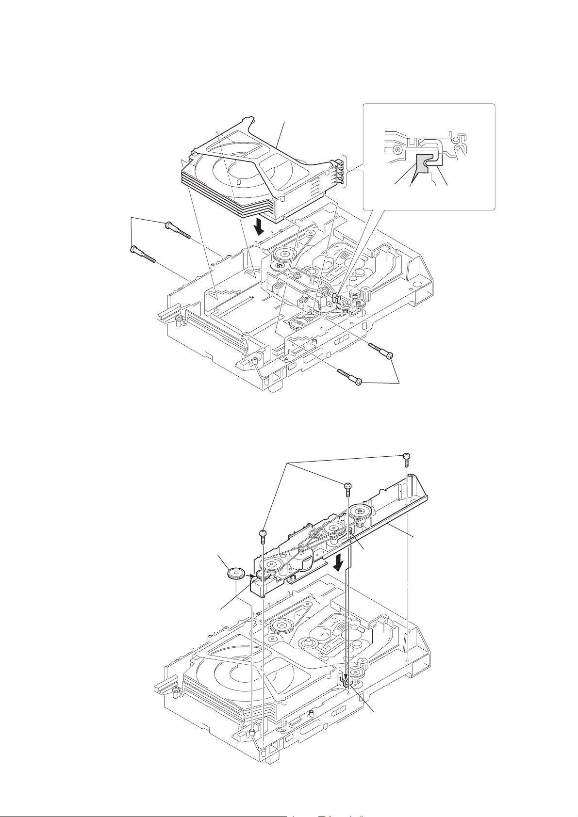
CD MECHANISM DECK SECTION
)
(CDM53E-K3BD37)
4
Remove the CD mechanism deck
section (CDM53E-K3BD37) in
the arrow A direction.
1
flat cable (17 core)
(12 cm) (CN112)
A
3
four screws
(BVTP3 × 10)
to fitting base (guide)
ass’y, bracket (chassis)
and magnet ass’y
(page 10)
2
connector
(CN713)
1
flat cable (19 core)
(CN501)
TAPE MECHANISM DECK SECTION
(TCM-230AWR2)
3
spring (eject A)
6
step screw
8
eject lever (A)
1
step screw
A
5
Remove the tape mechanism deck
section (TCM-230AWR2) in the
arrow A direction.
qs
shield plate
4
two screws
(BVTP3 × 10)
1
2
spring (eject B)
step screw
6
step screw
7
eject lever (B
q;
qa
bracket (MD A)
9
bracket (MD B)
two screws
(BVTT 2.6 × 6)
8
CD BASE UNIT (BU-K3BD37)
3
compression spring
(black)
4
CD base unit
(BU-K3BD37)
2
compression spring
(silver)
VIDEO BOARD
6
screw
(BVTT3 × 5)
3
flat cable (15core)
(CN713)
6
screw
(BVTT3 × 5)
8
screw
(BVTT3 × 5)
7
SVCD shield (U)
1
two screws
(PTPWH M2.6)
6
0
9
two screws
(BVTP3 × 8)
screw
(BVTT3 × 5)
VIDEO board
1
two screws
(PTPWH M2.6)
4
three screw
(BVTT3 × 8)
5
SVCD shield (B)
2
ground plate
1
two screws
(BVTT3 × 5 (S))
9
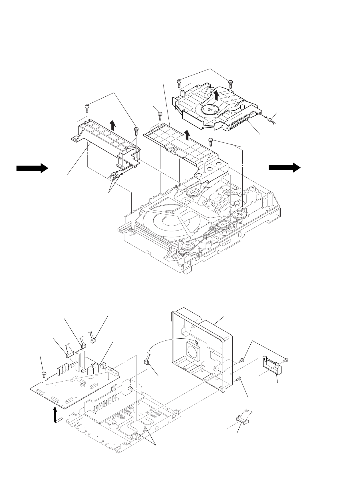
FITTING BASE (GUIDE) ASS’Y, BRACKET (CHASSIS) AND
MAGNET ASS’Y
5
bracket
(chassis)
two screws
(BVTP M2.6)
from CD mechanism
deck section
(CDM53E-K3BD37)
(page 8)
3
fitting base
(guide) ass’y
2
four screws
(BVTP M2.6)
1
two connectors
(CN709, 715)
4
7
four screws
(BVTP M2.6)
4
three screws
(BVTP M2.6)
6
connector
(CN710)
8
magnet ass’y
MAIN BOARD
6
connector
(CN109)
6
connector
(CN107)
7
two screws
(BVTP3
A
6
connector
(CN108)
9
Remove the MAIN board
in the arrow
×
8)
A
direction.
8
1
connector
(CN505)
two PC board
holders
5
back panel
2
three screws
(BVTP3
2
4
connection cord
(CN101)
×
10)
3
cover
(connector)
four screws
(BVTP3
×
10)
10

TRAY (SUB)
)
1
2
3
4
Rotating the pulley (LD), shift the slider (selection) in the arrow A direction.
Rotating the pulley (mode) in the arrow direction, adjust the tray (sub) to be removed.
Rotating the pulley (LD), shift the slider (selection) in the arrow B direction.
Rotating the pulley (mode) in the arrow direction, remove the tray (sub) to be removed.
pulley (LD)
stocker
section
tray (sub)
A
B
slider (selection)
pulley (mode)
CHASSIS (MOLD B) SECTION, STOCKER SECTION AND
SLIDER (SELECTION)
Note: In mounting the parts, refer to page 12 and 13.
5
stocker
section
pulley (LD)
4
two step
screws
6
two screws
(PTPWH M2.6)
7
slider (selection)
9
compression
spring
8
washer
1
three screws
(BVTP M2.6)
2
chassis (mold B) section
Note: Rotating the pulley (LD),
shift the slider (selection
to the left.
4
two step screws
3
gear (eject)
11
GEARS INSTALLATION
3
gear (gear B)
Adjust the gear (gear B) with the
portion A as shown.
1
Slide the slider (U/D)
fully in the arrow
direction.
2
gear (U/D slider)
slider (U/D) gear
portion A
4
gear (gear A)
gear
(gear B)
linearly
Adjust the gear so that it meshes with
the bottom tooth of slider (U/D) gear,
as shown.
SLIDER (SELECTION) INSTALLATION
2
gear (chucking)
rotary encoder
Align with the slot of
rotary encoder.
6
two screws
(PTPWH M2.6)
5
washer
4
compression spring
7
Adjust so as to be aligned with
gear (B) linearly, as shown.
Insert the slider (selection)
into the portion A.
portion A
12
1
rotary encoder
align marking
3
convex portion of
slider (selection)
gear (chucking)
Insert a convex portion into
a groove of gear (chucking).
STOCKER SECTION INSTALLATION
n
1
stocker section
2
portion A of tray (sub)
Hook the portion A of tray (sub)
to the slider (selection).
3
two step screws
CHASSIS (MOLD B) SECTION INSTALLATION
3
three screws
(BVTP M2.6)
potion A
of tray (sub)
3
sticking of
slider (selection)
two step screws
2
Insert the gear (eject)
under the gear (LD
deceleration).
gear (LD deceleration)
portion A
portion B of
slider (selection)
1
Insert the portion A of
chassis (mold B) sectio
into the portion B of
slider (selection).
13
SECTION 4
3
TEST MODE
[LED All Lit, Key Check Mode]
Procedure:
1. Press the ?/1 button to turn the power ON.
2. Press three buttons of s (DECK B), A (DISC 1), and
[DISC 5] simultaneously.
3. LEDs are all turned on.
Press the G (CD) button, and the key check mode is activated.
LEDs are all OFF.
4. When a button is pressed, the LED near the pressed button
blinks or lights up.
Also, if all buttons are pressed, all LEDs light up (not blink).
5. To release from this mode, press three buttons in the same
manner as step 2, or remove the power cord.
[CD Delivery Mode]
• This mode moves the optical pick-up to the position durable to
vibration. Use this mode when returning the set to the customer
after repair.
Procedure:
1. Press the ?/1 button to turn the power ON.
2. Press the s (DECK B) and [DISC 1] buttons simultaneously.
3. A message “LOCK” is displayed on the liquid crystal display
of the STR-NX300, and the CD delivery mode is set.
[Tape Deck Test Mode]
(In case of connected to the STR-NX300)
• If connected to the STR-NX300, the mode also acts as the STRNX300 amplifier test mode.
Procedure:
1. Press the ?/1 button to turn the power ON.
2. Press three buttons of s (DECK B), A (DISC 1), and S (CD)
simultaneously.
3. On liquid crystal display of the STR-NX300, the disc calen-
dar blinks, and “ALC OFF” is displayed, then the function
which was set before the test mode became active is displayed.
4. The automatic level control of the tape deck is in OFF status,
but while the
pressed during recording, automatic level control goes in ON
status.
[Tape Deck Test Mode]
(In case of connected to the power feed jig)
Procedure:
1. Turn on the Power switch on the power feed jig.
2. Press three buttons of s (DECK B), A (DISC 1),
and s (CD) simultaneously.
3. The G (CD) and S (CD) LEDs blink, and then pressing G
(CD), G / g (DECK A), or G / g (DECK B) button can
make each play possible.
4. Also, the other functions are enabled by pressing two buttons
simultaneously.
A combination of respective functions and buttons is as follows.
s (CD) and [REC PAUSE/START] buttons are
[VIDEO CD Color-bars Mode]
On this mode, the data of the color-bars signal as a picture signal
and the 1 kHz sine wave signal as a sound signal are output by the
mechanism controller (IC505) for the video CD signal check.
When measurement of the voltage and waveform on the VIDEO
board, perform it in this mode.
For reference, the color-bars signal can be observed at J502
(VIDEO OUT) and the sound signal can be observed at J101
(VIDEO/MD (AUDIO) OUT) (STR-NX300) using an oscilloscope.
Procedure:
1. Short the both ends of the land of SL503 of the VIDEO board.
2. Turn the power on. Press the [FUNCTION] button to select
CD.
3. The color-bars appears when the CD is in stop status, and it
disappears when the CD goes in play status.
4. After measuring, remove the lead wire connected.
– VIDEO board (Side B) –
CN501
IC505
SL501
SL502
SL50
CN502
function button
CD AMS – s (DECK A), S (CD)
AMS + s (DECK A), s (CD)
FR s (DECK B), S (CD)
FF s (DECK B), s (CD)
Deck-A REW/AMS – s (CD), g (DECK A)
FF/AMS + s (CD), G (DECK A)
Deck-B REW/AMS – s (CD), g (DECK B)
FF/AMS + s (CD), G (DECK B)
Note: Check that CD/TC signal change switch of relay connector jig is
set to the TC position.
14
SECTION 5
k
MECHANICAL ADJUSTMENTS
SECTION 6
ELECTRICAL ADJUSTMENTS
Precaution
1. Clean the following parts with a denatured alcohol-moistened
swab:
record/playback heads pinch rollers
erase head rubber belts
capstan idlers
2. Demagnetize the record/playback head with a head demagnetizer.
3. Do not use a magnetized screwdriver for the adjustments.
4. After the adjustments, apply suitable locking compound to the
parts adjusted.
5. The adjustments should be performed with the rated power supply voltage unless otherwise noted.
Torque Measurement
Mode
FWD
FWD
back tension
REV
REV
back tension
FF/REW
FWD tension
REV tension
Torque meter
CQ-102C
CQ-102C
CQ-102RC
CQ-102RC
CQ-201B
CQ-403A
CQ-403R
Meter reading
31 to 71 g • cm
(0.43 – 0.98 oz • inch)
2 to 6 g • cm
(0.03 – 0.08 oz • inch)
31 to 71 g • cm
(0.43 – 0.98 oz • inch)
2 to 6 g • cm
(0.03 – 0.08 oz • inch)
71 to 143 g • cm
(0.99 – 1.99 oz • inch)
100 g or more
(3.53 oz or more)
100 g or more
(3.53 oz or more)
TAPE DECK SECTION
0 dB=0.775 V
1. Demagnetize the record/playback head with a head demagnetizer.
2. Do not use a magnetized screwdriver for the adjustments.
3. After the adjustments, apply suitable locking compound to the
parts adjust.
4. The adjustments should be performed with the rated power
supply voltage unless otherwise noted.
5. The adjustments should be performed in the order given in
this service manual. (As a general rule, playback circuit adjustment should be completed before performing recording
circuit adjustment.)
6. The adjustments should be performed for both L-CH and RCH.
7. Switches and controls should be set as follows unless otherwise specified.
8. Set to the DOLBY NR OFF.
9. Set to the test mode. (See page 14)
10. When using the PFJ-1, disconnect a flat cable between CN111
(MAIN board) and CN502 (VIDEO board).
• Test Tape
Tape Signal Used for
P-4-A100 10 kHz, –10 dB Azimuth Adjustment
WS-48B 3 kHz, 0 dB Tape Speed Adjustment
P-4-L300 315 Hz, 0 dB Level Adjustment
Record/Playback Head Azimuth Adjustment
DECK A DECK B
Note: Perform this adjustments for both decks
Procedure:
1. Mode: Playback
test tape
P-4-A100
(10 kHz, –10 dB)
PFJ-1
set
or
STR-
NX300
AUDIO OUT jac
level meter
+
–
15
2. T urn the adjustment screw and check output peaks. If the peaks
k
do not match for L-CH and R-CH, turn the adjustment screw
so that outputs match within 1dB of peak.
Output
level
within
1dB
within
1dB
L-CH
peak
Tape Speed Adjustment DECK B
• Execute only if connected to the STR-NX300
Mode: Playback
test tape
WS-48B
(3 kHz, 0 dB)
set
STR-
NX300
AUDIO OUT jack
frequency counter
+
–
R-CH
Screw
position
peak
L-CH
peak
R-CH
peak
Screw
position
3. Mode: Playback
test tape
P-4-A100
(10 kHz, –10 dB)
L-CH
set
NX300
R-CH
waveform of oscilloscope
in phase 45°90°135°180
good
AUDIO OUT (L) jack
PFJ-1
or
STR-
AUDIO OUT (R) jack
wrong
L-CH
R-CH
°
oscilloscope
H
V
4. Repeat step 1 to 3 in playback (REV) mode.
5. After the adjustments, apply suitable locking compound to the
pats adjusted.
Adjustment Location:Playback Head (Deck A).
Record/Playback/Earth Head (Deck B).
1. Insert the WS-48B into the deck B.
2. Press the G (DECK B) button.
3. Press the [HI-DUB] button in playback mode.
Then at HIGH speed mode.
4. Adjust RV1001 on the LEAF SW board do that frequency
counter reads 6,000 ± 180 Hz.
5. Press the [HI-DUB] button.
Then back to NORMAL speed mode.
6. Adjust RV1002 on the LEAF SW board so that frequency
counter reads 3,000 ± 90 Hz.
Adjustment Location: LEAF SW board
Sample value of Wow and Flutter: 0.3% or less W.RMS (JIS)
(WS-48B)
Playback level Adjustment
DECK A DECK B
Procedure:
Mode: Playback
test tape
P-4-L300
(315 Hz, 0 dB)
set
PFJ-1
STR-
NX300
or
AUDIO OUT jac
level meter
+
–
Deck A is RV311 (L-CH) and RV411 (R-CH), Deck B is RV301
(L-CH) and RV401 (R-CH) so that adjustment within specified
value as follows.
Specified Value:
AUDIO OUT jack PB level: 301.5 to 338.3 mV (–8.2 to –7.2
dB) level
difference between the channels: within ± 0.5 dB
16
Adjustment Location: AUDIO board
Open the cassette holder
and unhock six claws of
the sub panel (TC2)
with tweezers or something,
then remove the sub panel (TC2).
forward
reverse
REC Bias Adjustment DECK B
RV401
RV301
RV341
RV311
RV411
IC602
CN601
LR
RL
RV441
PB LEVEL
– DECK B –
REC BIAS
LR
PB LEVEL
– DECK A –
RV351
(R-CH)
RV301
(L-CH)
IC301
REC
LEVEL
CN301
1
3
Procedure:
1. Mode: Record
Specified value:
AUDIO OUT jack PB level: 47.2 to 53.0 mV (–24.3 to –23.3 dB)
Adjustment Location: MAIN board
AUDIO IN jack
50 mV (–23.8 dB)
600
Ω
PFJ-1
or
STR-
NX300
blank tape
CN-123
set
AF OSC
1) 315 Hz
2) 10 kHz
attenuator
2. Mode: Playback
recorded
portion
set
PFJ-1
or
STR-
NX300
level meter
+
–
AUDIO OUT jack
3. Confirm playback the signal recorded in step 1 become specified value as follows.
If these values are out of specified value, adjust the RV341
(L-CH) and RV441 (R-CH) on the AUDIO board to repeat
steps 1 and 2.
Specified value: Playback output of 315 Hz to playback
output of 10 kHz: ± 0.5 dB
Adjustment Location: AUDIO board
– MAIN BOARD (Conductor Side) –
– AUDIO BOARD (Component Side) –
REC Level Adjustment DECK B
Procedure:
1. Mode: Record
AUDIO IN jack
315 Hz, 50 mV (–23.8 dB)
AF OSC
attenuator
600
Ω
PFJ-1
or
STR-
NX300
set
blank tape
CN-123
2. Mode: Playback
recorded
portion
set
PFJ-1
or
STR-
NX300
level meter
+
–
AUDIO OUT jack
3. Confirm playback the signal recorded in step 1 become specified value as follows.
If these values are out of specified value, adjust the RV301
(L-CH) and R V351 (R-CH) on the MAIN board to repeat steps
1 and 2.
– LEAF SW BOARD (Component Side) –
TAPE SPEED
(NORMAL) (HIGH)
RV1002
RV1001
CN1001
17
CD SECTION
+
–
BD board
TP (RF)
TP (VC)
oscilloscope
V
Note:
1. CD Block is basically designed to operate without adjustment. Therefore, check each item in order given.
2. Use YEDS-18 disc (3-702-101-01) unless otherwise indicated.
3. Use an oscilloscope with more than 10 MΩ impedance.
4. Clean the object lens by an applicator with neutral detergent when the
signal level is low than specified value with the following checks.
5. Use the following extension cables and relay connector.
• Extension cable (19P) (Part No. J-2501-011-B)
Relay connector (Part No. J-2501-167-A)
(BD board CN101 to VIDEO board CN501)
• Extension cable (17P) (with connector) (Part No. J-2501-167-A)
(CONNECTOR board CN701 to MAIN board CN112)
6. Perform measurement by connecting to the STR-NX300.
1. S-CURVE CHECK
oscilloscope
BD board
TP (FEO)
TP (VC)
+
–
2. RF LEVEL CHECK
Procedure:
1. Connect oscilloscope to TP (RF).
As TP (RF) and TP (VC) are located at the edge of board, clip
them together with the board using alligator clips.
2. Turn the power ON.
3. Load a disc (YEDS-18) and playback.
4. Confirm that oscilloscope waveform is clear and check RF
signal level is correct or not.
Note: Clear RF signal waveform means that the shape “ ” can be clearly
distinguished at the center of the waveform.
RF signal waveform
VOLT/DIV: 200 m
TIME/DIV: 500 ns
Procedure:
1. Connect oscilloscope to TP (FEO).
2. Connect between TP (FEO) and TP (VC) by lead wire.
3. Connect between TP (A GCCON) and TP (GND) by lead wire.
4. Turn the power ON.
5. Load a disc (YEDS-18) and turn the power ON again and actuate the focus search. (Actuate the focus search when disc
tray is moving in and out)
6. Check the oscilloscope waveform (S-curve) is symmetrical
between A and B. And confirm peak to peak level within 2.4
± 0.7 Vp-p.
S-curve waveform
symmetry
A
within 2.4
B
±
0.7 Vp-p
7. After check, remove the lead wire connected in step 2.
Note: • Try to measure several times to make sure than the ratio of A : B
or B : A is more than 10 : 7.
• Take sweep time as long as possible and light up the brightness
to obtain best waveform.
level:
1.2
±
0.2 Vp-p
18
Connecting points:
+
–
TP (27 MHz)
VIDEO board
frequency counter
TP
(GND)
CT503
VIDEO
Frequency
Adjustment
TP
(27 MHz)
CN501
SL501
SL502
SL503
CN502
IC505
D502
– BD BOARD (Side B) –
TP
TP
(VC)
(RF)
TP
(AGCCON)
IC103
(FEO)
TP (FEI)
IC102
IC101
TP
TP
(TEO)
(GND)
TP
VIDEO SECTION
Note:
1. Perform measurement by connecting to the STR-NX300.
Frequency Adjustment
Connection:
Procedure:
1. Connect the frequency counter to TP (27 MHz) on VIDEO
board.
2. Turned power switch on.
3. Press the [FUNCTION] button to select the CD.
4. Adjust CT503 on the VIDEO board so that the frequency
counter reading 27.0 MHz ± 80 Hz at stop status.
Adjustment Location:
– VIDEO Board (Side B) –
– MAIN BOARD (Conductor Side) –
IC101
SL101
(ADJ)
19
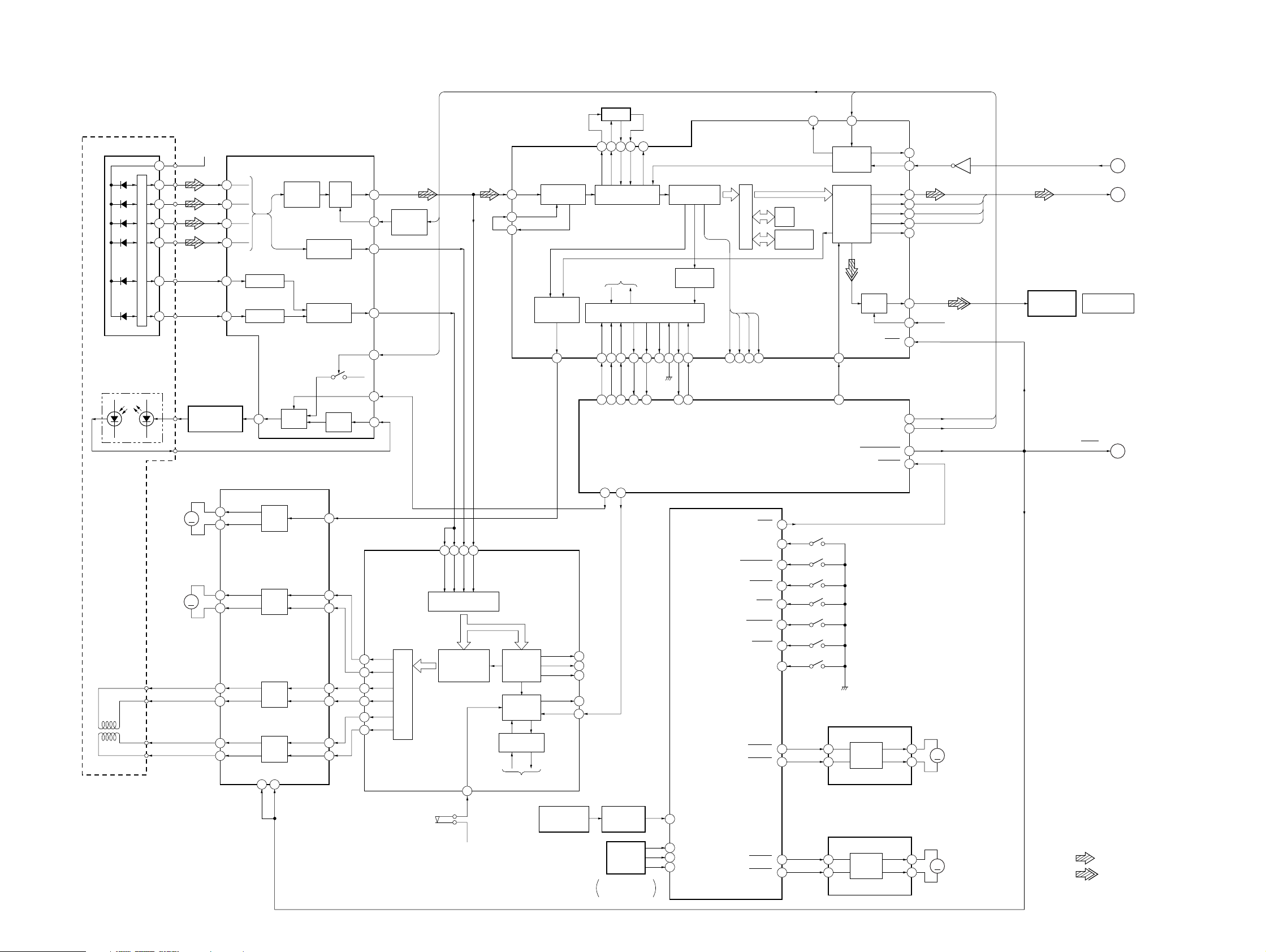
7-1. BLOCK DIAGRAM – SERVO Section –
RF AMP,
DETECTOR
A
B
C
D
I-V AMP
F
E
OPTICAL PICK-UP BLOCK
(KSS-213B/Z-N)
CD A+5V
7
4
2
1
5
10
6
10
11
FOCUS/TRACKING ERROR AMP
A
5
B
6
C
7
D
8
F
F I-V AMP
E
E I-V AMP
IC103
RF
SUMMING
AMP
SECTION 7
DIAGRAMS
RFO
RF EQ
AMP
FOCUS
ERROR AMP
TRACKING
ERROR AMP
RFE
HOLD SW
16
15
FE
14
TE
13
21
CTL2
RF EQ
SWITCH
Q102
CTL1
DIGITAL SIGNAL PROCESSOR
IC101 (1/2)
RFAC
50
49
48
ASYMMETRY
CORRECTOR
ASYI
ASYO
DIGITAL
CLV
PROCESSOR
MDP
25 76 77
FILTER
53 55
FILI
PCO
FILO
CLTV
DIGITAL PLL
TO SERVO AUTO
SEQUENCER
CPU INTERFACE
SENSE
DATA
CLOK
XLAT
125254
XPCK
EFM
DEMODULATOR
32K
RAM
INTERNAL BUS
SUBCODE
PROCESSOR
EXCK
SCOR
SBSO
SQCK
SQSO
79 801574 6 5 10 111368 3
WFCK
XUGF
GFS
EMPH
ERROR
CORRECTOR
16 69
C4M
CLOCK
GENERATOR
DIGITAL
INTERFACE
MUTE
D/A
CTL1
XTSL
DIGITAL
OUT
XTAO
XTAI
PCMD
BCK
LRCK
C2PO
WDCK
DOUT
MD2
XRST
HTC-NX300
72
71
66
67
65
14
17
64
63
2
IC104
DATA
BCK
LRCK
C2PO
CD A+5V
OPTICAL
TRANSCEIVER
IC207
MCLK
33.8MHz
DATA, BCK,
LRCK, C2PO
CD DIGITAL OUT
OPTICAL
A
B
(Page 22)
(Page 22)
LASER DIODE
2-AXIS
DEVICE
(TRACKING)
(FOCUS)
LDON
22
AUTOMATIC
POWER CONTROL
LD
PD
M101
(SPINDLE)
M102
(SLED)
Q101
FOCUS/TRACKING COIL DRIVE,
VO3 (+)
15
M
M
VO3 (–)
16
VO4 (+)
17
VO4 (–)
18
VO2 (+)
12
VO2 (–)
11
VO1 (+)
14
VO1 (–)
13
LD
APC LD
3
AMP
SPINDLE/SLED MOTOR DRIVE
IC102
OPIN3 (–)
MOTOR
DRIVE
OPIN4 (+)
MOTOR
OPIN4 (–)
DRIVE
OPIN2 (+)
COIL
OPIN2 (–)
DRIVE
OPIN1 (+)
COIL
OPIN1 (–)
DRIVE
STBY2STBY1
209
APC PD
AMP
23
27
26
5
6
2
3
PD
4
DIGITAL SERVO
SFDR
29
SRDR
30
TFDR
31
TRDR
32
FFDR
33
FRDR
34
PROCESSOR
IC101 (2/2)
PWM GENERATOR
FOCUS/TRACKING/SLED
40 41 39 43
FE
TE
SE
RFDC
A/D
CONVERTER
FOCUS/
TRACKING/SLED
SERVO DSP
SSTP
26
MIRR,
DFCT, FOK
DETECTOR
SERVO
INTERFACE
SERVO AUTO
SEQUENCER
TO CPU INTERFACE
FOK
MIRR
DFCT
COUT
SCLK
3 5 4 1 18 36 37 10
SCOR
SENSE
DSP CLK
DSP DATA
DSP LATCH
SENSE CLK
LDON
6 2
22
20
21
19
8
SUBQ CLK
SUBQ DATA
CD MECHANISM CONTROLLER
IC505 (1/2)
SYSTEM CONTROLLER
IC101 (1/3)
XRST
PRTC SW
MIDOUT SW
OUT SW
IN SW
MIDIN SW
INIT SW
CNT SW
LOD NEG
LOD POS
4
56
60
58
59
61
57
93
63
65
CTRL1
11
19
DSP MUTE
S702
S701
S708
S704
S703
S705
S706
LOADING MOTOR DRIVE
IN1
3
IN2
6
CTRL2
XRESET
OUT1
OUT2
77
12
7
M
2
(LOADING)
DEVICE RESET
S702 (LID)
(ON: When CD lid is close.)
S701 (MID OUT)
(ON: When tray is going to open/close.)
S708 (OUT)
(ON: When tray is open.)
S704 (IN)
(ON: When sub tray set to play position.)
S703 (MID IN)
(ON: When sub tray move between tray and stocker.)
S705 (INIT)
(ON: When elevator down to bottom.)
S706 (COUNT)
(ON: When elevator up/down each sub tray stock position.)
IC702
MOTOR
DRIVE
M702
CTL1
CTL2
RESET
C
(Page 22)
S101
05
(LIMIT)
CD A+5V
DISC IN DETECT
SENSOR
D704,Q703
LEVEL SHIFT
Q701
ROTARY
ENCODER
S707
DISC TRAY
ADDRESS DETECT
92
70
69
68
DISC SENS
ENCODE0
ENCODE1
ENCODE2
CLP POS
CLP NEG
ELEVATOR
UP/DOWN MOTOR DRIVE
IC701
• SIGNAL PATH
IN1
67
66
3
IN2
6
MOTOR
DRIVE
OUT1
OUT2
7
M
2
M701
(ELEVATOR UP/DOWN)
: CD PLAY
: DIGITAL OUT
2121
HTC-NX300
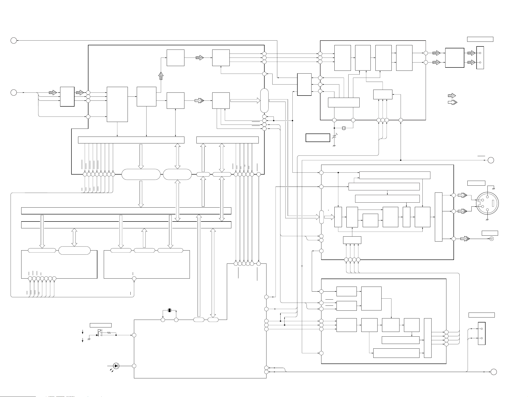
7-2. BLOCK DIAGRAM – AUDIO/VIDEO CD Section –
MCLK 33.8MHz
A
(Page 21)
B
(Page 21)
DATA, BCK,
LRCK, C2PO
05
DATA
BCK
LRCK
C2PO
A0-A11
A0-A10, BA
LDQM
CS
RAS
CAS
WE
15 16 17 18 14 80 84 22
UDQM
LDQM
CS
RAS
CAS
WE
LEVEL
SHIFT
IC501
2, 3, 5, 6, 8, 9, 11, 12, 39
40, 42, 43, 45, 46, 48, 49
SD-CLK
UDQM
CLK
D0-D15
DQ0-DQ15
MPEG VIDEO/AUDIO DECODER,
VIDEO SIGNAL PROCESSOR
IC505
CD-DATA
4
CD-BCK
3
CD-LRCK
5
CD-C2PO
6
SD-RAS
SD-CS0
MWE
ROM-CS
128
82 90 86 85 35 36 79 15 16 13
RAS
CS
WE
CE
D-RAM
IC507
S501
SYSTEM SELECT
NTSC
AUTO
PAL
CD-ROM
INTERFACE
CIRCUIT
SD-CLK
UDQM
LDQM
SD-CAS
UDQM
CLK
CAS
LDQM
12 – 5, 27, 26, 23 13 – 15, 17 – 21 25, 4, 28, 29, 3, 2, 3021 – 24, 27 – 32, 20, 19
D502
(SELF DIAGNOSIS)
D-RAM/ROM INTERFACE
104, 106, 110, 112, 111, 108,
105, 102, 99, 96, 100, 98, 114,
116, 118, 120, 121, 122, 124
ADDRESS BUS
DATA BUS
A0-A10
A0-A10 O0-O7 A11-A17
CE
93
73
MA0-MA7
A0-A17
CE
NT/PAL
TEST LED
MPEG
SYSTEM
DECODER
D0-D7
MPEG
AUDIO
DECODER
MPEG
VIDEO
DECODER
MD0-MD5
54, 58, 60, 64, 68,
72, 74, 78, 76, 73, 70,
66, 62, 59, 56, 53,
D0-D15
A11-A17
PROGRAM ROM
IC508
X501
10MHz
15
13
AUDIO
INTERFACE
CIRCUIT
VIDEO
PROCESS
CIRCUIT
CPU INTERFACE
HA0-HA2
202 – 204
A0-A2
A0-A2
71 – 73 81 – 88
A2-A0XOUTXIN
CD MECHANISM CONTROLLER
HD0-HD7
2 – 4, 6, 8 – 11
D0-D7
D0-D7
D0-D7
IC505 (1/2)
VDATA0-VDATA7
WAIT
INTCSR/W
206 207 208
39 20
47 46 44 24
8830-CS
8830 HINT
BUS-XRDY
DA-DATA
DA-BCK
DA-LRCK
DA-XCLK
SYSCLK
VCK-IN
HSYNC
VSYNC
RD
BUS-XRD
BUS-XWR
NT/PAL OUT
DF LATCH
CLK1
DATA1O
OSD CS
I2C/RX
I2C/TX
161
167
166
169
150, 152, 154, 155
142, 143, 145, 148,
178
177
HSYNC
157
VSYNC
158
RESET
8830 RESET
21
22
33
31
28
DATA
29
CLK
30
LATCH
OSC
BUFFER
IC504
VIDEO FREQUENCY
HSYNC
VSYNC
HSYNC
VSYNC
CT503
(27MHz)
18
17
19
21
20
4
51
22
28
27
29
8
20
19
1
3
2
4
DATA
BCK
LRCK
768FSO
384FSO
MCKO
2 – 8, 10
INTERFACE
TIMING CONTROL/
CLOCK GENERATOR
XT2
24 1
VCLK
NTB
YUV0
YUV7
HSY
VSY
PIXCLK
OSC IN
HSYNC
VSYNC
CLK
DATA
CS
RESET
INPUT
CIRCUIT
X503
27MHz
LATCH
OSD-SW
15
BLKRG
CLOCK
CONTROL
PROTECTIVE
CIRCUIT
INTERFACE
CIRCUIT
XT1
RGB
OSD
ROSD
GOSD
57 64 1
DIGITAL FILTER,
D/A CONVERTER
IC509
DIGITAL
FILTER,
NOISE
SHAPER
CIRCUIT
MODE/FIELD/FLAME CONTROL
SUB CARRIER BURST GENERATOR
FILTER
BOSD
B
HORIZONTAL/
VIRTICAL
CONTROL
ADDRESS
REGISTER
U/V
CONVERTER
MODE
CONTROL
MDMCML
DATA
D/A
8 7 109
CLK
VIDEO TIMING CONTROL
DISPLAY/BACKGROUND
LATCH
Y-LEVEL
ADJ.
CHROMA
GEN.
DATA
SELECTOR
CHARACTOR ROM
CONTROL
LOW-PASS
FILER
RSTB
VOUTL
14
VOUTR
11
MIX
SIGNAL
SYNC
BURST
Y/C FILTER
DIGITAL RGB ENCODER
ON SCREEN
DISPLAY CONTROLLER
VIDEO
RAM
D/A CONVERTER
IC514
B-BLK
V-R
V-G
V-B
OUTPUT CONTROL
LOW-PASS
FILER
IC101
• SIGNAL PATH
: CD PLAY (AUDIO)
: CD PLAY (VIDEO)
COUT
37
YOUT
45
VOUT
39
BLK
15
R
16
G
17
B
18
CN101 (1/4)
SYSTEM CONTROL
(TO STR-NX300AV)
3
CD. L
2
CD. R
RESET
(Page 21)
J301
S VIDEO OUT
C
3
4
Y
VIDEO OUT
CN101 (2/4)
SYSTEM CONTROL
(TO STR-NX300AV)
14
DATA
17
CLK
DATA,
CLK
C
1
2
J302
IIC DATA
IIC CLK
D
(Page 24)
2222
7-3. BLOCK DIAGRAM – TAPE DECK Section –
HP101
(PLAYBACK)
L-CH
R-CH R-CH
HRPE101 (1/2)
(RECORD/PLAYBACK)
L-CH
R-CH R-CH
3
R-CH
PB EQ AMP
(DECK A)
IC611
PB EQ AMP
(DECK B)
IC601
REC/PB SWITCHING
IC602
1
R-CH
RV311
PB LEVEL (L)
(DECK A)
RV301
PB LEVEL (L)
(DECK B)
4
DECK PROCESS
DECK A/B SELECT, PB/REC EQ AMP,
DOLBY NR AMP, ALC, AMS
AIN (L)
48
BIN (L)
46
BIAS (N)
33
BIAS (C)
32
BIAS (M)
31
A 120/70
19
S1004
(DECK A 120/70)
S1008
(DECK B 120/70)
IC301
BIAS
CONTROL
CIRCUIT
B NORM/CROM
ALC ON/OFF
NORM/HIGH
PB A/B
1516182022 23242517
70
120
R-CH
NR ON/OFF
BIAS ON/OFF
RM ON/OFF
L.P.F.
BUFFER
28
27
AMS
CIRCUIT
REC/PB/PASS
LM ON/OFF
26
+
MAOUT
MSIN
MSOUT
RIN (L)
43
ALC (L)
44
DOLBY PASS
ALC
ROUT (L)
35 34
DOLBY NR
AMP
CIRCUIT
ALC
IN (L)
REC OUT (L)
39
RV301
REC LEVEL (L)
(DECK B)
EQ IN (L)
38
REC
EQ AMP
PB OUT (L)
EQ OUT
HTC-NX300
• SIGNAL PATH
: PLAYBACK (DECK A)
: PLAYBACK (DECK B)
: RECORD
CN101 (3/4)
SYSTEM CONTROL
(TO STR-NX300AV)
40
R-CH
(L)
36
7
PB-L
9
PB-R
6
REC-L
4
REC-RR-CH
RV441
REC BIAS (R)
(DECK B)
HRPE101 (2/2)
(ERASE)
R-CH
05
2
RV341
REC BIAS (L)
(DECK B)
BIAS OSC
T621
BIAS OSC
Q621, 622
REC BIAS
SWITCH
Q623
C331, L331
BIAS
TRAP
B+
(A+7V)
D+5V
100
TC-RELAY
(DECK A PLAY)
8584838281 807978
PB-A/B
EQ-H/N
ALC-ON/OFF
A-PLAY-SW
87
S1001
S1002
(DECK B PLAY)
BIAS
REC-MUTE
B-PLAY-SW
86
TC-MUTE
R/P-PASS
NR-ON/OFF
(DECK A HALF)
S1003
77
AMS-IN
A-HALF
88
ROTATION
DETECT SENSOR
(DECK A)
IC1001
91
A-SHUT
S1006
(DECK B HALF)
S1005
(DECK A REC)
S1009
(DECK B REC)
ROTATION
DETECT SENSOR
(DECK B)
IC1002
90
B-SHUT
SYSTEM CONTROLLER
B-HALF
89
IC101 (2/3)
TRIGGER PLUNGER
DECK A
TRIGGER
PLUNGER DRIVE
(DECK A)
Q333, 334
73
A-TRG
TRIGGER PLUNGER
DECK B
TRIGGER
PLUNGER DRIVE
(DECK B)
Q331, 332
72
B-TRG
Q335
76
CAP-M-H/L
RV1001
TAPE SPEED
(HIGH)
CAPM-CNT1
CAPM-CNT2
CAPSTAN MOTOR
CONTROL SWITCH
Q1001
75
MOTOR DRIVE
74
RV1002
TAPE SPEED
(NORMAL)
CAPSTAN
Q336 – 343
M
M1
(CAPSTAN)
2323
 Loading...