

Page 1
HCD-CPX1
SERVICE MANUAL
Ver 1.0 2003.04
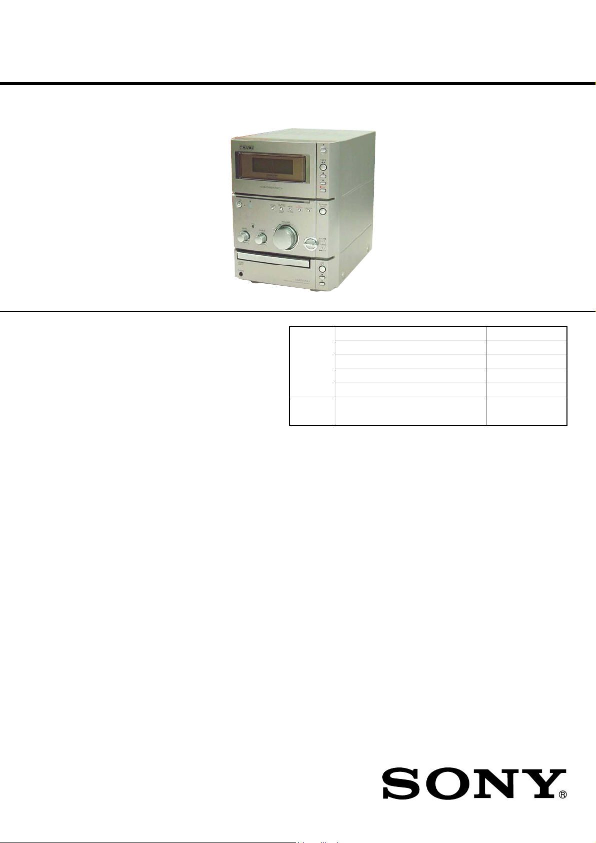
HCD-CPX1 is the Amplifier, CD
player, Tape Deck and Tuner section
in CMT-CPX1.
CD
Section
Tape deck
Section
US Model
Canadian Model
E Model
Austr alian Model
Model Name Using Similar Mechanism NEW
CD Mechanism Type CDM55A-K6BD44S
Base Unit Name BU-K6BD44S
Optical Block Name KSM-213DCP
Optical Pick-up Name KSS-213D
Model Name Using Similar Mechanism NEW
Amplifier section
For the U.S. model
AUDIO POWER SPECIFICATIONS
POWER OUTPUT AND TOTAL HARMONIC
DISTORTION:
With 4-ohm loads, both channels driven, from
100 – 10,000 Hz: rated 70 watts per channel
minimum RMS power, with no more than 10%
total harmonic distortion from 250 milliwatts to
rated output.
North American model:
Continuous RMS power output (reference):
Total harmonic distortion less than 0.9% (4 ohms at
1kHz, 35 W)
Other models:
The following measured at 220 – 240 V AC, 50/60 Hz
DIN power output (rated): 55 + 55 W
70 + 70 W
(4 ohms at 1 kHz, 10%
THD)
(4 ohms at 1 kHz, DIN)
SPECIFICATIONS
Continuous RMS power output (reference):
Inputs
MD (VIDEO) IN (phono jacks):
Outputs
CD DIGITAL OUT: Optical Wavelength:
PHONES: accepts headphones with
SPEAKER: accepts impedance of
CD player section
Laser Semiconductor laser
Frequency response CD: 2 Hz – 20 kHz
Wavelength 780 – 790 nm
70 + 70 W
(4 ohms at 1 kHz, 10%
THD)
Sensitivity 450/250 mV,
impedance 47 kilohms
660 nm
an impedance of 8 ohms or
more
4ohms
(CD: λ=780 nm)
Emission duration:
continuous
Tape deck section
Recording system 4-track 2-channel stereo
Frequency response 50 – 13,000 Hz (± 3 dB),
Tuner section
FM stereo, FM/AM superheterodyne tuner
FM tuner section
Tuning range
North American model: 87.5 – 108.0 MHz
Other models: 87.5 – 108.0 MHz (50 kHz
Antenna FM wire antenna
Antenna terminals 75 ohms unbalanced
Intermediate frequency 10.7 MHz
AM tuner section
Tuning range
Pan-American model: 530 – 1,710 kHz
using Sony TYPE I
cassettes
(100 kHz step)
step)
(with the tuning interval
set at 10 kHz)
Other models: 530 – 1,710 kHz
Antenna AM loop antenna, external
Intermediate frequency 450 kHz
General
Power requirements
North American model: 120 V AC, 60 Hz
Australian model: 230 – 240 V AC, 50/60 Hz
Korean model: 220 V AC, 60 Hz
Other models: 220 – 240 V AC, 50/60 Hz
Power consumption: 50 W
Dimensions (w/h/d):
Mass:
Design and specifications are subject to change
without notice.
(with the tuning interval
set at 10 kHz)
531 – 1,602 kHz
(with the tuning interval
set at 9 kHz)
antenna terminal
Approx. 174 × 240.5 × 291
mm
Approx. 4.3 kg
COMPACT DISC DECK RECEIVER
9-877-173-01 Sony Corporation
2003D0500-1 Home Audio Company
C 2003.04 Published by Sony Engineering Corporation
Page 2
HCD-CPX1
r
Notes on chip component replacement
•Never reuse a disconnected chip component.
• Notice that the minus side of a tantalum capacitor may be damaged by heat.
Flexible Circuit Board Repairing
•Keep the temperature of the soldering iron around 270 ˚C during repairing.
• Do not touch the soldering iron on the same conductor of the
circuit board (within 3 times).
• Be careful not to apply force on the conductor when soldering
or unsoldering.
SAFETY CHECK-OUT
After correcting the original service problem, perform the following safety check before releasing the set to the customer:
Check the antenna terminals, metal trim, “metallized” knobs,
screws, and all other exposed metal parts for AC leakage.
Check leakage as described below.
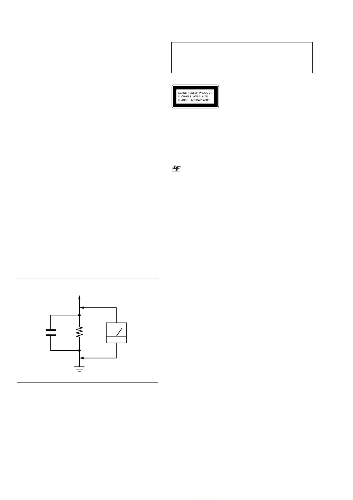
LEAKAGE TEST
The AC leakage from any exposed metal part to earth ground and
from all exposed metal parts to any exposed metal part having a
return to chassis, must not exceed 0.5 mA (500 microamperes.).
Leakage current can be measured by any one of three methods.
1. A commercial leakage tester , such as the Simpson 229 or RCA
WT -540A. Follo w the manufacturers’ instructions to use these
instruments.
2. A battery-operated AC milliammeter. The Data Precision 245
digital multimeter is suitable for this job.
3. Measuring the voltage drop across a resistor by means of a V OM
or battery-operated A C voltmeter . The “limit” indication is 0.75
V, so analog meters must have an accurate low-voltage scale.
The Simpson 250 and Sanwa SH-63Trd are examples of a
passive VOM that is suitable. Nearly all battery operated digital
multimeters that have a 2 V AC range are suitable. (See Fig. A)
CAUTION
Use of controls or adjustments or performance of procedures
other than those specified herein may result in hazardous radiation exposure.
This appliance is
classified as a CLASS 1
LASER product. This
label is located on the
rear exterior.
UNLEADED SOLDER
Boards requiring use of unleaded solder are printed with the leadfree mark (LF) indicating the solder contains no lead.
(Caution: Some printed circuit boards may not come printed with
the lead free mark due to their particular size)
: LEAD FREE MARK
Unleaded solder has the following characteristics.
• Unleaded solder melts at a temperature about 40 ˚C higher than
ordinary solder.
Ordinary soldering irons can be used but the iron tip has to be
applied to the solder joint for a slightly longer time.
Soldering irons using a temperature regulator should be set to
about 350 ˚C.
Caution: The printed pattern (copper foil) may peel away if the
heated tip is applied for too long, so be careful!
• Strong viscosity
Unleaded solder is more viscou-s (sticky, less prone to flow)
than ordinary solder so use caution not to let solder bridges occur such as on IC pins, etc.
• Usable with ordinary solder
It is best to use only unleaded solder but unleaded solder may
also be added to ordinary solder.
To Exposed Metal
Parts on Set
1.5 k
0.15 µF
Fig. A. Using an AC voltmeter to check AC leakage.
SAFETY-RELATED COMPONENT WARNING!!
COMPONENTS IDENTIFIED BY MARK 0 OR DOTTED
LINE WITH MARK 0 ON THE SCHEMATIC DIAGRAMS
AND IN THE PARTS LIST ARE CRITICAL TO SAFE
OPERATION. REPLACE THESE COMPONENTS WITH
SONY PARTS WHOSE PART NUMBERS APPEAR AS
SHOWN IN THIS MANUAL OR IN SUPPLEMENTS PUBLISHED BY SONY.
Ω
Earth Ground
AC
voltmete
(0.75 V)
ATTENTION AU COMPOSANT AYANT RAPPORT
À LA SÉCURITÉ!
LES COMPOSANTS IDENTIFIÉS P AR UNE MARQUE 0
SUR LES DIAGRAMMES SCHÉMATIQUES ET LA LISTE
DES PIÈCES SONT CRITIQUES POUR LA SÉCURITÉ
DE FONCTIONNEMENT. NE REMPLACER CES COMPOSANTS QUE PAR DES PIÈCES SONY DONT LES
NUMÉROS SONT DONNÉS DANS CE MANUEL OU
DANS LES SUPPLÉMENTS PUBLIÉS PAR SONY.
2
Page 3

TABLE OF CONTENTS
HCD-CPX1
1. SERVICING NOTES............................................... 4
2. GENERAL
Location of Controls ....................................................... 8
Setting the Clock............................................................. 9
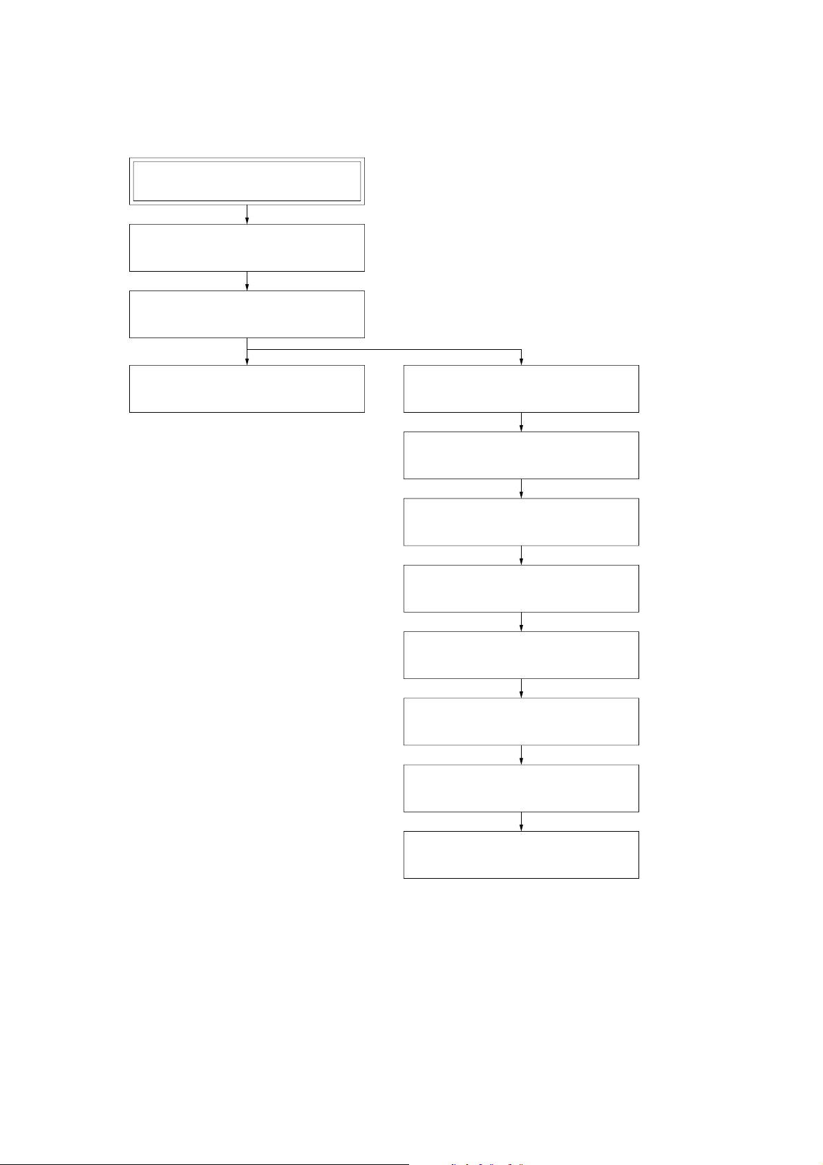
3. DISASSEMBLY
3-1. Disassembly Flow ........................................................... 10
3-2. Case ................................................................................. 11
3-3. Front Panel Section ......................................................... 11
3-4. TC Board, Mechanical Deck .......................................... 12
3-5. MAIN Board ................................................................... 12
3-6. Tuner Unit ....................................................................... 13
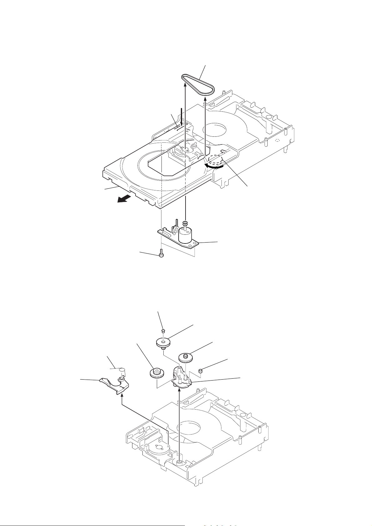
3-7. CD Mechanism Deck (CDM55A-K6BD44S)................ 13
3-8. Loading Board................................................................. 14
3-9. Cam (CDM55) ................................................................ 14
3-10. Base Unit (BU-K6BD44S) ............................................. 15
3-11. Motor Gear Assy (Sled) (M102), BD Board .................. 15
3-12. Optical Pick-up (KSS-213D) .......................................... 16
4. TEST MODE.............................................................. 17
5. ELECTRICAL ADJUSTMENTS
Deck Section ................................................................... 19
CD Section ...................................................................... 20
6. DIAGRAMS
6-1. Block Diagram – CD Servo Section –........................... 21
6-2. Block Diagram – TUNER/TAPE DECK Section – ...... 22
6-3. Block Diagram – MAIN Section – ................................ 23
6-4. Block Diagram
– DISPLAY/POWER SUPPLY Section – ...................... 24
6-5. Note for Printed Wiring Boards and
Schematic Diagrams ....................................................... 25
6-6. Printed Wiring Board – BD Board – ............................. 26
6-7. Schematic Diagram – BD Board – ................................ 27
6-8. Printed Wiring Board – TC Board – .............................. 28
6-9. Schematic Diagram – TC Board –................................. 29
6-10. Printed Wiring Boards
– LOADING/MAIN Boards – ....................................... 31
6-11. Schematic Diagram – MAIN Board (1/2) – .................. 32
6-12. Schematic Diagram
– LOADING/MAIN (2/2) Boards – ............................... 33
6-13. Printed Wiring Board – AMP Board – .......................... 34
6-14. Schematic Diagram – AMP Board – ............................. 35
6-15. Printed Wiring Boards
– BACK LIGHT/LCD/SWITCH Boards – .................... 36
6-16. Schematic Diagram
– BACK LIGHT/LCD/SWITCH Boards – ................... 37
6-17. Printed Wiring Boards
– HP/SP OUT/POWER Boards – .................................. 38
6-18. Schematic Diagram
– HP/SP OUT/POWER Boards – ................................. 39
6-19. IC Pin Function Description ........................................... 44
7. EXPLODED VIEWS
7-1. Case Section .................................................................... 47
7-2. Front Panel Section-1...................................................... 48
7-3. Front Panel Section-2...................................................... 49
7-4. Lid (TC) Section ............................................................. 50
7-5. Chassis Section-1 ............................................................ 51
7-6. Chassis Section-2 ............................................................ 52
7-7. Chassis Section-3 ............................................................ 53
7-8. CD Mechanism Deck Section
(CDM55A-K6BD44S) .................................................... 54
7-9. Base Unit (BU-K6BD44S) ............................................. 55
8. ELECTRICAL PARTS LIST ............................... 56
3
Page 4
HCD-CPX1
)
SECTION 1
SERVICING NOTES
NOTES ON HANDLING THE OPTICAL PICK-UP
BLOCK OR BASE UNIT
The laser diode in the optical pick-up block may suffer electrostatic break-down because of the potential difference generated
by the charged electrostatic load, etc. on clothing and the human
body.
During repair, pay attention to electrostatic break-down and also
use the procedure in the printed matter which is included in the
repair parts.
The flexible board is easily damaged and should be handled with
care.
NOTES ON LASER DIODE EMISSION CHECK
The laser beam on this model is concentrated so as to be focused
on the disc reflective surface by the objective lens in the optical
pick-up block. Therefore, when checking the laser diode emission, observe from more than 30 cm away from the objectiv e lens.
MODEL IDENTIFICATION
– Back Panel –
Part No.
Model Name Part No.
US and Canadian models 4-244-015-1
Singapore model 4-244-015-2
Australian model 4-244-015-3
Korean model 4-244-015-4
[]
[]
[]
[]
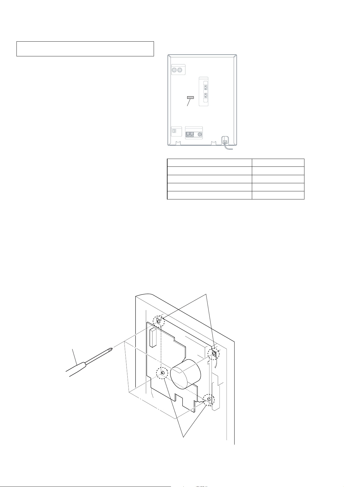
NOTE ON INSTALLING AND REMOVING THE TAPE MECHANICAL DECK
To prevent four screws of +BVTP 3 × 8 TYPE 2 TT (B), that fix the mechanical deck to the front panel, from being magnetized, must not
use a magnetic screwdriver.
screw +BVTP 3 × 8 TYPE 2 TT (B
non-magnetic screwdriver
screw +BVTP 3 × 8 TYPE 2 TT (B)
4
Page 5
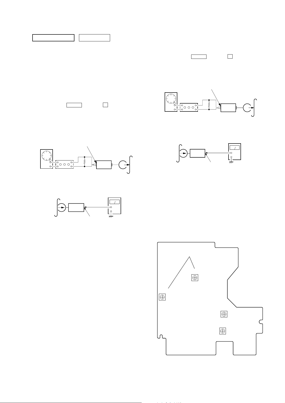
TAPE MECHANICAL DECK SERVICE POSITION
l
Set up the service position with putting an insulator under the mechanical deck as the figure shown below.
tape mechanical deck
insulator
HCD-CPX1
CD MECHANISM DECK SERVICE POSITION
Set up the service position for the CD mechanism deck with disassembling the entire set as the figure shown below.
main board
AMP section
front pane
CD mechanism deck
5
Page 6
HCD-CPX1
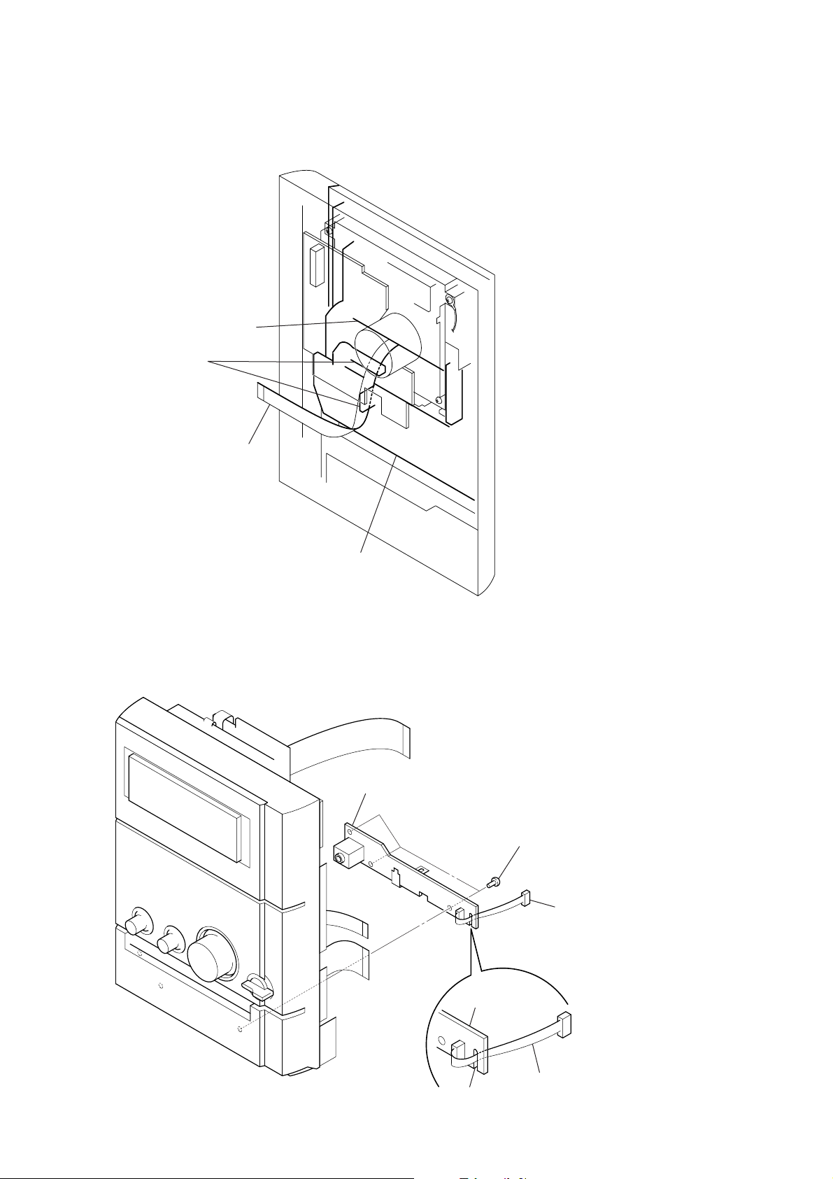
NOTE ON LEADING THE WIRE (FLAT TYPE) (9 CORE)
Lead the wire (flat type) (9 core) properly to prevent the wire from coming out from the right side of the guides on the sub panel or sagging
inside of the lid.
lid (TC)
guides
wire (flat type) (9 core)
sub panel
NOTE ON INSTALLING THE HP BOARD
Note: Follow the assembly procedure in the numerical order given.
2
HP board
3
three screws
(BVTP2.6
×
8)
1
Lead the cable trough out
the ditch of the HP board
to prevent the cable from
contacting with the CD
mechanism deck.
HP board
cable
ditch
6
Page 7
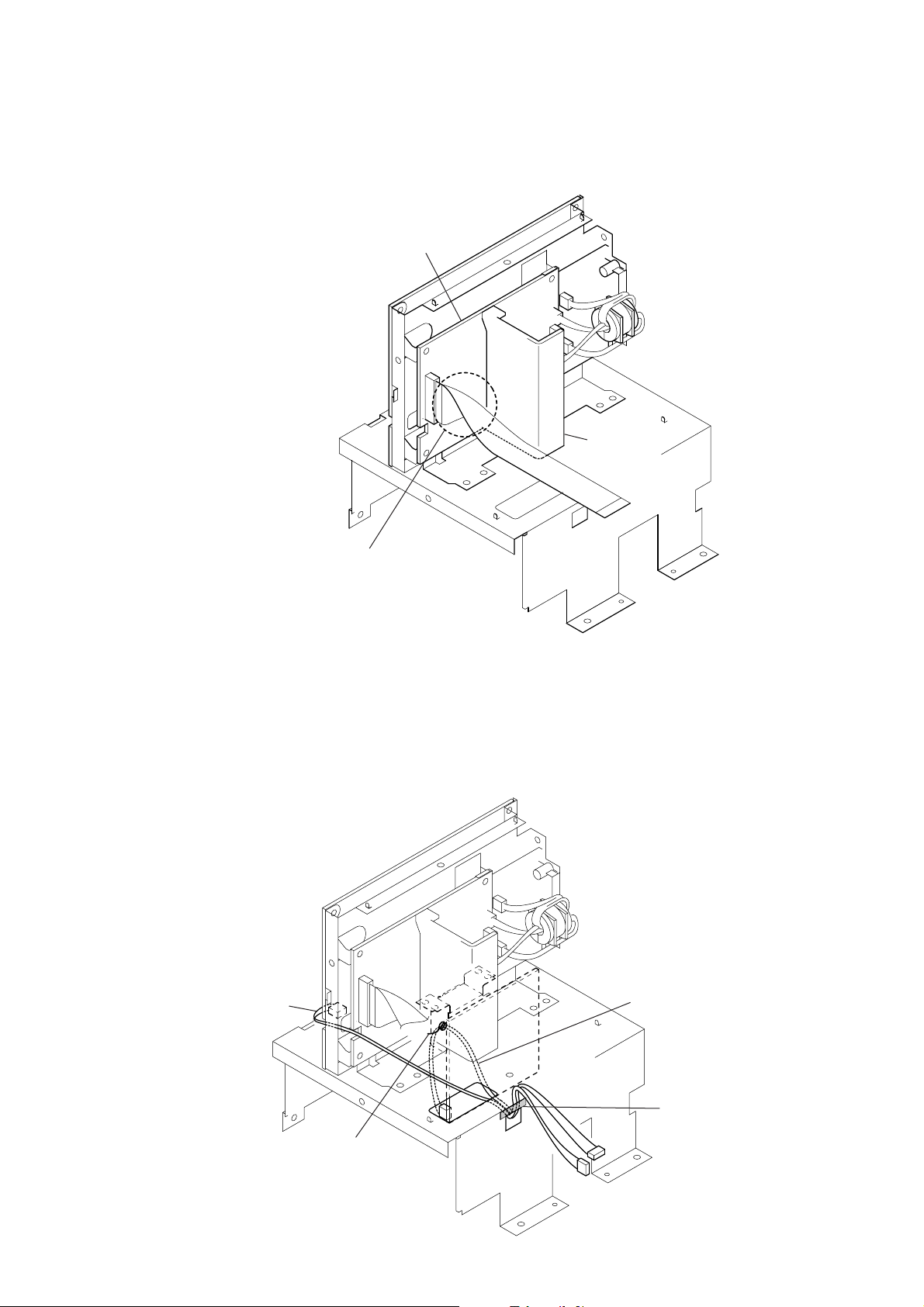
CLINCHING THE WIRE (FLAT TYPE) (21 CORE)
c
AMP board
HCD-CPX1
heat sink
Clinch the wire (flat type) (21 core)
to prevent the wire from contacting with
the heat sink of the AMP board.
HANDLING TWO CABLES FROM THE SUB POWER AND THE SWITCHING REGULA TOR TO THE MAIN BOARD
Note: Fix two cables with the lead pin and the fabric non woven (10 – 20),
or they may sag and contact with the CD mechanism deck.
cable from the switching
regulator to the main board
cable from the sub power
to the main board
lead pin
fabric no woven (10 – 20)
Note: Do not reuse the current fabri
because it may fall off.
7
Page 8
HCD-CPX1
• LOCATION OF CONTROLS
– Front View –
SECTION 2
GENERAL
This section is extracted from
instruction manual.
ALPHABETICAL ORDER
A – Q
BASS +/– wa
CD SYNCHRO qa
Disc tray ql
DISPLAY wf
Display window 3
DSG ws
FM MODE qs
FUNCTION 0
PHONES jack qk
PLAY MODE/DIRECTION wd
1
wf
wd
ws
wa
w;
ql
qk
R – Z
Remote sensor 2
REPEAT qs
TREBLE +/– w;
TUNER/BAND 9
TUNING MODE wd
TUNING +/– qd
VOLUME +/– qf
2
3
BUTTON DESCRIPTIONS
?/1 (power) 1
TAPE Z (eject) 4
TAPE nN (play) 5
TAPE x (stop) 6
TAPE X (pause) 7
TAPE z REC (record) 8
lm/ML (rewind/fast
forward, go back/go forward)
qd
CD NX (play pause) qg
CD x (stop) qh
CD Z (eject) qj
4
5
6
7
8
9
0
qa
qs
qd
qf
qg
qh
qj
8
Page 9
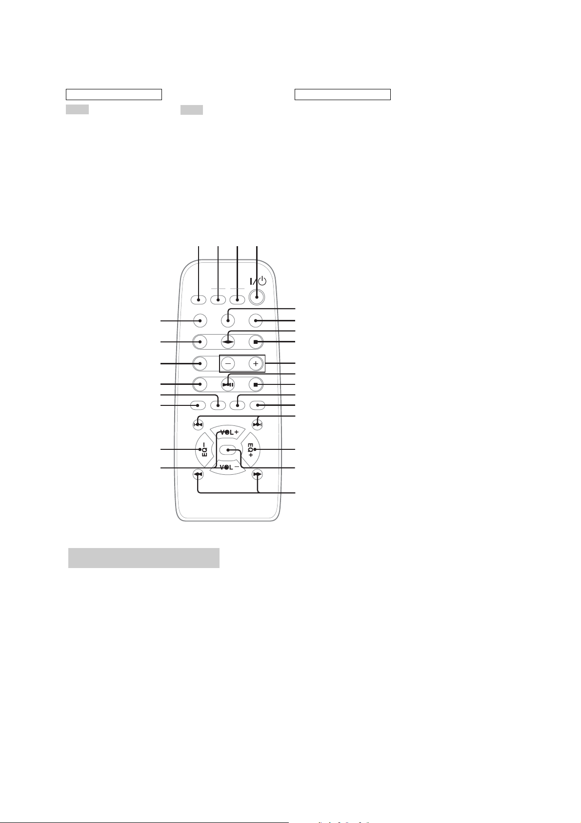
– Remote Control –
HCD-CPX1
ALPHABETICAL ORDER
A – E
CD ws
CLEAR w;
CLOCK/TIMER SELECT 2
CLOCK/TIMER SET 3
DISPLAY 6
ENTER qd
EQ qh
EQ + qg
EQ – ql
wg
wf
wd
ws
wa
w;
F – Z
FUNCTION wg
PLAY MODE wa
REPEAT qs
SLEEP 1
TAPE wf
TUNER/BAND wd
TUNER MEMORY 5
TUNING MODE wa
TUNING +/– 9
VOL +/– qk
2 3
14
BUTTON DESCRIPTIONS
?/1 (power) 4
TAPE nN (play) 7
TAPE x (stop) 8
CD NX (play pause) 0
CD x (stop) qa
./> (go back/go forward)
qf
m/M (rewind/fast forward)
qj
5
6
7
8
9
0
qa
qs
qd
qf
ql
qk
Setting the clock
1 Press ?/1 to turn on the system.
2 Press CLOCK/TIMER SET.
3 Press . or > repeatedly to set the
hour.
4 Press ENTER.
5 Press . or > repeatedly to set the
minute.
6 Press ENTER.
The clock starts working.
To adjust the clock
1 Press CLOCK/TIMER SET.
2 Press . or > until “CLOCK” appears,
then press ENTER.
3 Do the same procedures as step 3 to 6
above.
Note
The clock is not displayed in Power Saving Mode.
qg
qh
qj
9
Page 10
HCD-CPX1
• This set can be disassembled in the order shown below.
3-1. DISASSEMBLY FLOW
Set
3-2. CASE
(Page 11)
3-3. FRONT PANEL SECTION
(Page 11)
SECTION 3
DISASSEMBLY
3-4. TC BOARD, MECHANICAL DECK
(Page 12)
3-5. MAIN BOARD
(Page 12)
3-6. TUNER UNIT
(Page 13)
3-7. CD MECHANISM DECK
(CDM55A-K6BD44S)
(Page 13)
3-8. LOADING BOARD
(Page 14)
3-9. CAM (CDM55)
(Page 14)
3-10. BASE UNIT (BU-K6BD44S)
(Page 15)
3-11. MOTOR GEAR ASSY (SLED) (M102),
BD BOARD
(Page 15)
10
3-12. OPTICAL PICK-UP (KSS-213D)
(Page 16)
Page 11
Note: Follow the disassembly procedure in the numerical order given.
)
HCD-CPX1
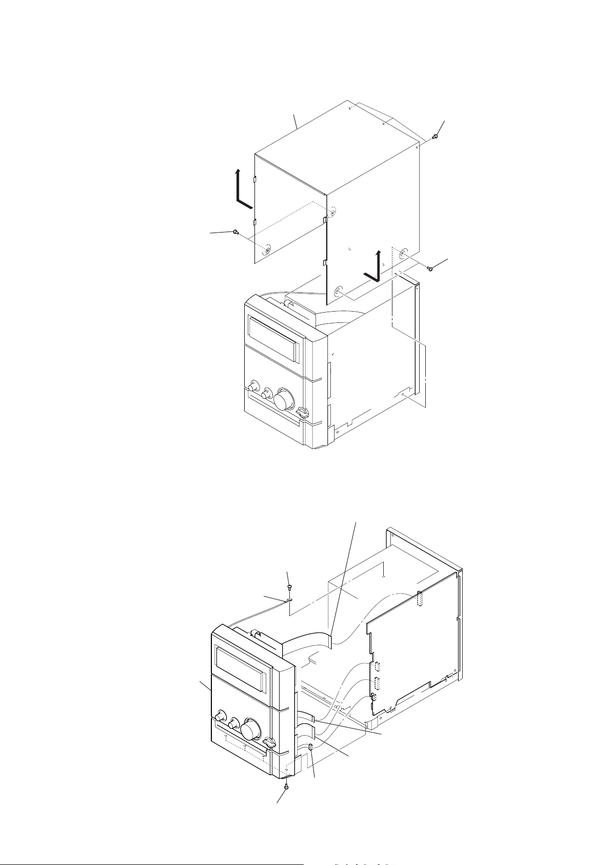
3-2. CASE
1
two case screws
3
4
case
3
2
three screws
(BVTP3
1
two case screws
×
6)
3-3. FRONT PANEL SECTION
2
ground wire lead
6
front panel section
5
four screws
(BVTP3
1
screw
(BVTP3
×
6)
3
wire (flat type) (19 core)
(CN221)
×
6)
3
wire (flat type) (9 core
(CN403)
3
wire (flat type) (19 core)
(CN402)
4
connector
(CN102)
11
Page 12
HCD-CPX1
)
s
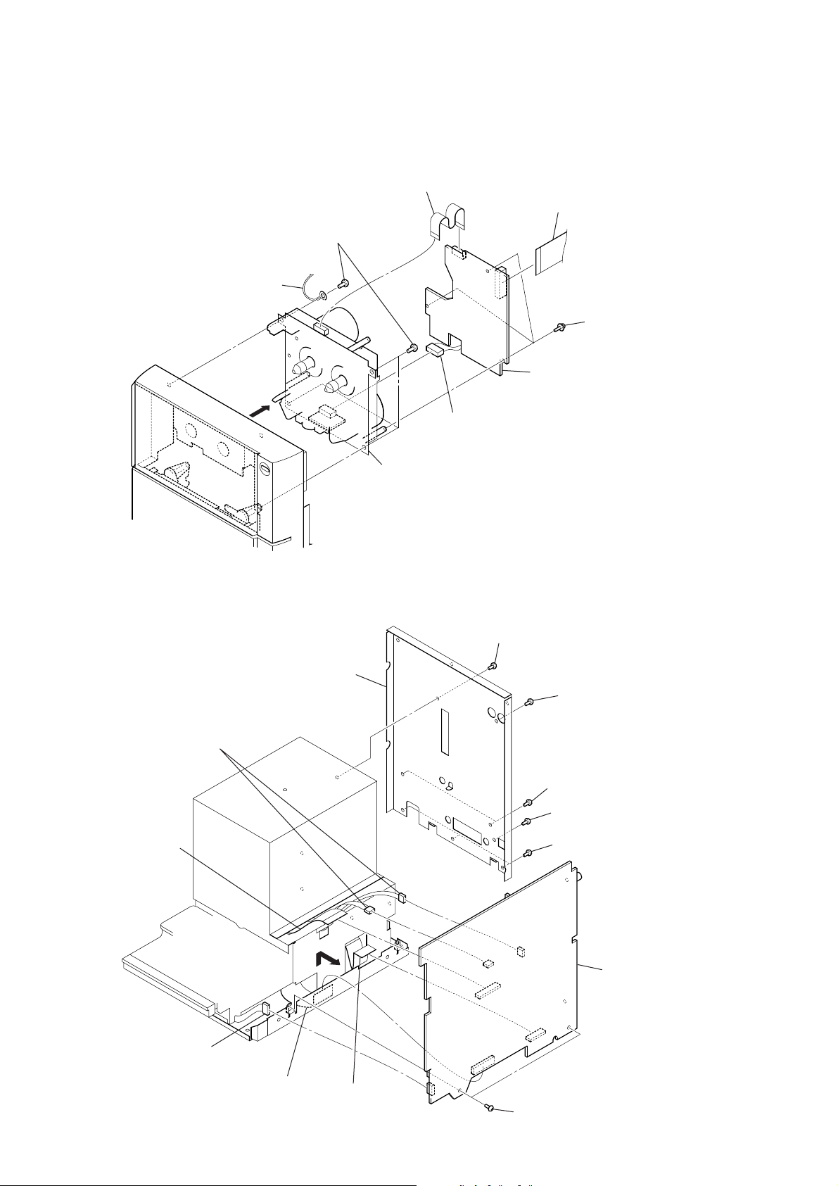
3-4. TC BOARD, MECHANICAL DECK
6
four screws
(BVTP3
Note: Must not use a magnetic
7
ground wire lead
×
8)
screwdriver to prevent the screws
from being magnetized.
2
wire (flat type) (8 core)
(CN602)
3
connector
1
wire (flat type) (19 core)
(CN603)
4
three screw
(PTPWH 2)
5
TC board
3-5. MAIN BOARD
7
6
wire (flat type) (21 core)
(CN101)
two connectors
(CN301, CN401)
3
back panel
8
mechanical deck
1
screw
(BVTP3
×
6)
2
screw
(BVTP3
1
two screws (BVTP3 × 6)
2
screw (BVTP3 × 8)
1
three screws (BVTP3 × 6
×
8)
12
7
connector
(CN201)
6
wire (flat type)
(21 core)
(CN202)
5
6
wire (flat type)
(11 core)
(CN211)
8
4
two screws (BVTP3 × 6)
main board
Page 13
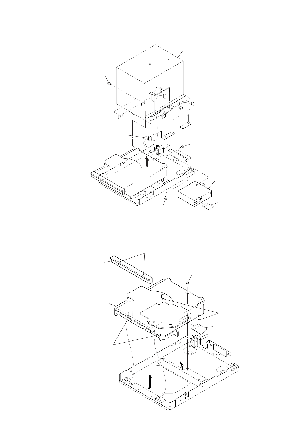
3-6. TUNER UNIT
)
)
2
two screws
(BVTP3
×
6)
1
connector
(CN990)
3
bracket
5
two screws
(BVTP3
HCD-CPX1
×
6)
2
two screws
(BVTP3
3-7. CD MECHANISM DECK (CDM55A-K6BD44S)
1
two claws
2
CD lid
9
CD mechanism deck (CDM55A-K6BD44S)
6
tuner unit
4
wire (flat type) (11 core
×
6)
3
screw
4
two bosses
8
wire (flat type) (21 core
(CN1101)
6
two claws
7
5
13
Page 14
HCD-CPX1
)
3-8. LOADING BOARD
3
Pull the tray (CDM55D) pushing B.
B
2
belt (CDM55)
A
1
Rotate the gear(A) in
the direction of arrow
A
.
3-9. CAM (CDM55)
2
lever (SW)
1
torsion spring
4
two screws
(BTP2.6
6
×
8)
gear (A)
3
spacer (55)
4
pulley (LDG)
5
loading board
5
gear (B)
7
roller
8
cam (CDM55
14
Page 15
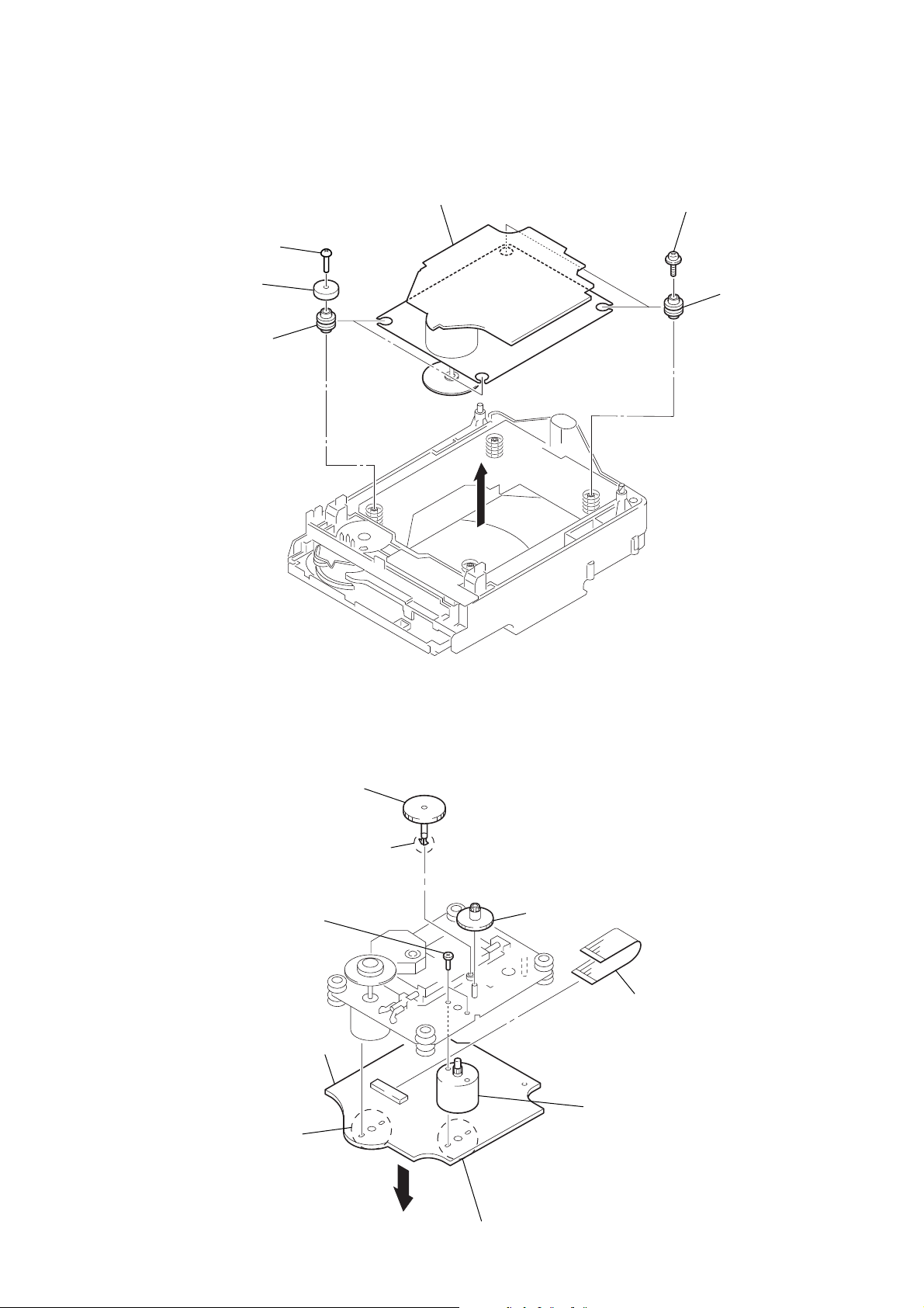
3-10. BASE UNIT (BU-K6BD44S)
)
2
two screws
(BTTP M2.6)
3
two stoppers (BU)
5
two insulators
6
base unit (BU-K6BD44S)
1
two floating screws
(PTPWHM2.6)
5
two insulators
HCD-CPX1
4
3-11. MOTOR GEAR ASSY (SLED) (M102), BD BOARD
6
gear (A)
5
claw
8
two screws
×
3)
(M2
7
gear (B)
1
Remove two
solders.
4
BD board
2
1
Remove two solders.
3
wire (flat type) (16 core
(CN102)
9
motor gear assy (SLED)
(M102)
15
Page 16
HCD-CPX1
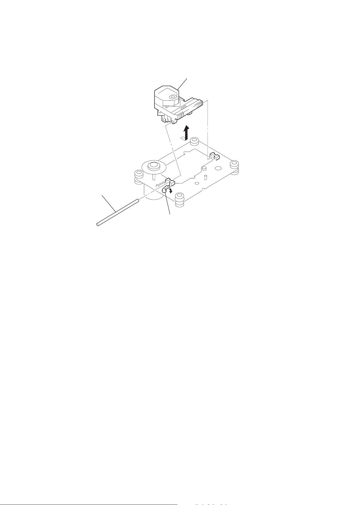
3-12. OPTICAL PICK-UP (KSS-213D)
3
Remove the optical pick-up
(KSS-213D) in the direction
of arrow
B
B
.
2
sled shaft
A
1
Slide the lever
in the direction of arrow
A
.
16
Page 17

SECTION 4
TEST MODE
HCD-CPX1
[CMN (MC) TEST MODE]
•This mode is used to check operations of Amplifier.
Procedure:
1. Press the ?/1 key to turn the power ON.
2. Press three keys of [DSG], [REPEAT] and [DISPLAY]
simultaneously.
3. When the CMN (MC) test mode is activated, “s” blinks on
the liquid crystal display.
4. Turn the [BASS] knob counterclockwise, “TONE MIN” is
displayed on the liquid crystal display. Turn the [BASS] knob
clockwise, “TONE MAX” is displayed on the liquid crystal
display.
Turn the [TREBLE] knob clockwise or counterclockwise,
“TONEFLAT” is displayed on the liquid crystal display.
Turn the [VOLUME] knob counterclockwise, “VOL MIN” is
displayed on the liquid crystal display. Turn the [VOLUME]
knob clockwise, “VOL MAX” is displayed on the liquid crystal
display.
5. To release this mode, press the ?/1 key.
[PANEL (GC) TEST MODE]
•This mode is used to check the liquid crystal display, LED,
model, destination, software version and key.
Procedure:
1. Press the ?/1 key to turn the power ON.
2. Press three keys of [DSG], [PLAY MODE] and [DISPLAY]
simultaneously.
3. Liquid crystal display and LEDs are all turned on.
4. When you want to enter the model, destination and version
display mode, press the [REPEAT] key. The model and
destination are displayed alternately on the liquid crystal display.
5. Each time [REPEAT] key is pressed, the display changes starting
from MD version, MC version, GC version, CD version, CDD
version, CDMA version, CDMB version, BDA version, BDB
version, ST version, TA version, TM version, and TC version
this order, and returns to the MD version display on the liquid
crystal display.
6. When
7. Press the [PLAY MODE] key, the key check mode is activated.
8. In the key check mode, the liquid crystal display displays “K0”.
9. To release this mode, press three keys in the same manner as
[FUNCTION] key is pressed while the version numbers
are being displayed except model and destination, year, month
and day of the software creation display. When [FUNCTION]
key is pressed again, the display returns to the software version
display. When [REPEAT] key is pressed while year, month and
day of the software creation are being displayed, the year, month
and day of creation of the software versions are displayed on
the liquid crystal display in the same order of version display.
Each time a key is pressed, “K” value increases. Ho wever , once
a key is pressed, it is no longer taken into account.
step 2, or disconnect the power cord.
[COLD RESET]
• The cold reset clears all data including preset data stored in the
RAM to initial conditions. Execute this mode when returning
the set to the customer.
Procedure:
1. Press the ?/1 key to turn the power ON.
2. Press three keys of ?/1 , x (CD) and x (TAPE) simultaneously .
3. The liquid crystal display becomes blank instantaneously, and
the set is reset.
[SHIP MODE (NO MEMORY CLEAR) ]
•This mode moves the optical pick-up to the position durable to
vibration. Use this mode when returning the set to the customer
after repair.
Procedure:
1. Press the ?/1 key to turn the power ON.
2. Press the [FUNCTION] key to select “CD”.
3. Press three keys of Z (CD), x (CD) and [DISPLAY]
simultaneously.
4. After the “STANDBY” display blinks, “LOCK” is displayed
on the liquid crystal display, and the ship mode is set.
[SHIP MODE (MEMORY CLEAR) ]
• This mode moves the optical pick-up to the position durable to
vibration. Use this mode when returning the set to the customer
after repair.
Procedure:
1. Press the ?/1 key to turn the power ON.
2. Press the [FUNCTION] key to select “CD”.
3. Press three keys of Z (CD), CD NX and [DISPLAY]
simultaneously.
4. After the “STANDBY” display blinks, “LOCK” is displayed
on the liquid crystal display, and the ship mode is set.
[CD TRAY LOCK MODE]
• This mode is used to unable to take sample disc out of tray in
the shop.
Procedure:
1. Press the ?/1 key to turn the power ON.
2. Press the [FUNCTION] key to select “CD”.
3. While pressing the Z (CD) key, press the x (CD) key fo r 5
seconds.
4. The message “LOCKED” is displayed on the liquid crystal
display and the tray is locked. (Even if pressing the
key, the message “LOCKED” is displayed on the liquid crystal
display and the tray is locked)
5. To release from this mode, pressing the Z (CD) key, press the
x (CD) key for 5 seconds.
6. The message “UNLOCKED” is displayed on the liquid crystal
display and the tray is unlocked.
Z (CD)
[TUNER STEP CHANGE MODE]
(Singapore, Korean and Australian models)
•A step of AM channels can be changed over between 9 kHz and
10 kHz.
Procedure:
1. Press the ?/1 key to turn the power ON.
2. Press the [FUNCTION] key to select “TUNER”, and press the
[BAND] key to select “AM”.
3. Press the ?/1 key to turn the power OFF.
4. Press two keys of ?/1 and M L simultaneously.
5. The message “AM 9K STEP” or “AM 10K STEP” is displayed
on the liquid crystal display, and thus the channel step is changed
over.
[CD SERVICE MODE]
•This mode can run the CD sled motor freely . Use this mode, for
instance, when cleaning the optical pick-up.
Procedure:
1. Press the ?/1 key to turn the power ON.
2. Press the [FUNCTION] key to select “CD”.
3. Press three keys of [DSG] , [REPEAT] and x (T APE) sim ul-
taneously.
4. Press the M L key to move the optical pick-up to outside
track, or press the l m key to inside track.
5. To release this mode, press the ?/1 key.
17
Page 18
HCD-CPX1
[AGING MODE]
• This mode can be used for operation check of CD section and
tape deck section.
CD section and tape deck section work in parallel.
If an error occurred:
The aging operation stops only an error occurred sections and
display then status.
If no error occurs:
The aging operation continues repeatedly.
Procedure:
1. Press the ?/1 key to turn the power ON.
2. Press the [FUNCTION] key to select “CD”.
3. Set disc on the tray and set tape into the deck.
4. Press the [REPEAT] key to “REPEAT” off.
5. Press three keys of [DSG], [PLAY MODE] and x (TAPE)
simultaneously.
6. Aging operations of CD and tape are started at the same time.
7. To release this mode, press the ?/1 key.
1. Display at the Aging Mode
Display operating state of CD section and tape deck section
alternately.
If an error occurred, stop display which that section.
2. CD Section
The sequence during the aging mode is following as below.
Display at the aging mode is the same as the normal operation.
Aging mode sequence (CD section) :
Start
Disc chucking
TOC read
3. Tape Deck Section
The sequence during the aging mode is following as below.
If an error occurred, stop display that step.
Display at the aging mode is “TAPE AG—”.
Aging mode sequence (Tape deck section) :
Start
Rewind the tape
Shut off
FWD play the tape
2 minutes
Fast forward the tape
Shut off or 20 seconds
REV play the tape
2 minutes
[CD ERROR CODE MODE]
• This mode can be used for error display of CD section.
Procedure:
1. Press the ?/1 key to turn the power ON.
2. Press the [FUNCTION] key to select “CD”.
3. Press three keys of [DSG], [REPEAT] and X simultaneously.
Note: Error code is not displayed on the liquid crystal display.
[CD SERVO TEST MODE]
• This mode used to ckeck operation of optical pick-up.
Procedure:
1. Press the ?/1 key to turn the power ON.
2. Press the [FUNCTION] key to select “CD”.
3. Press three keys of [DSG], [PLAY MODE] and X simultaneously .
4. When the CD servo test mode is activated, optical pick-up moves.
Play first track for 2 seconds
Play last track for 2 seconds
Open the disc tray
Close the disc tray
[5 REPEAT OFF MODE]
• Number of repeat for CD playback is 5 times when the repeat
mode is “REPEAT”. This mode is used to enables CD to repeat
playback for limitless times.
Procedure:
1. Press the ?/1 key to turn the power on.
2. Press the [FUNCTION] key to select “CD”.
3. Press three keys of [DSG], M L and x (TAPE)
simultaneously.
4. When the 5 repeat off mode is activated, “LIMIT OF” is
displayed on the liquid crystal display.
[CHANGE-OVER FUNCTION OF EXTERNAL INPUT]
• This mode is used to enable function of external input to change
over between MD and VIDEO.
Procedure:
1. Set to standby state.
2. Press two keys of ?/1 and [FUNCTION] simultaneously.
3. The function of external input changes over to MD or VIDEO.
18
Page 19
set
MAIN board
MD (VIDEO) IN (J101)
315 Hz, 34.6 mV (–27 dB)
blank tape
CS-123
600
Ω
attenuator
AF OSC
SECTION 5
(R-CH)
(L-CH)
RV603
(R-CH)
RV602
(L-CH)
RV652
RV653
– TC BOARD (Component Side) –
REC Level Adjustment
REC Bias
Adjustment
ELECTRICAL ADJUSTMENTS
HCD-CPX1
DECK SECTION
Note: Confirm each contents of this section first of all. If the results are
not satisfied, do the adjustment.
1. The adjustments should be performed with the rated power supply
voltage unless otherwise noted.
2. The adjustments should be performed in the order given in this service
manual.
3. The adjustments should be performed for both L-CH and R-CH.
0 dB=0.775 V
REC BIAS ADJUSTMENT
Procedure:
1. Press the [FUNCTION] key to select “MD” or “VIDEO”.
2. Set the tape into the deck.
3. After pressi ng z REC key, press X (TAPE) key to start
recording.
4. Mode: Record
MAIN board
MD (VIDEO) IN jack (J101)
L-CH, R-CH
34.6 mV (– 27 dB)
600
Ω
set
blank tape
CN-123
AF OSC
1) 315 Hz
2) 10 kHz
attenuator
REC LEVEL ADJUSTMENT
Procedure:
1. Press the [FUNCTION] key to select “MD” or “VIDEO”.
2. Set the tape into the deck.
3. After pressi ng z REC key, press X (TAPE) key to s tart
recording.
4. Mode: Record
5. Mode: Playback
recorded
portion
set
SP OUT board
SPEAKER terminals (J701)
L-CH, R-CH
level meter
+
–
5. Mode: Playback
recorded
portion
6. Confirm the playback signal recorded in step 3 becomes
adjustable level as follows.
If these levels are out of specified values, adjust the RV653 (LCH) and R V603 (R-CH) on the TC board to repeat steps 4 and
5.
Specified values: Playback output of 315 Hz to playback
output of 10 kHz: ± 2.0 dB
Adjustment Location: TC board
level meter
set
SP OUT board
SPEAKER terminals (J701)
L-CH, R-CH
6. Confirm the play back signal recorded in step 3 becomes
adjustable level as follows.
If these levels are out of specified v alues, adjust the RV652 (LCH) and RV602 (R-CH) on the TC board to repeat steps 4 and
+
–
5.
Specified values: Playback level 30.8 to 38.8 mV (–28 to –26 dB)
Adjustment Location: TC board
19
Page 20
HCD-CPX1
V
CD SECTION
Note:
1. CD Block is basically constructed to operate without
adjustment.
2. Use YEDS-18 disc (3-702-101-01) unless otherwise indicated.
3. Use an oscilloscope with more than 10 MΩ impedance.
4. Clean the object lens by an applicator with neutral detergent
when the signal level is low than specified value with the
following checks.
5. Check the focus bias check when optical pick -up block is
replaced.
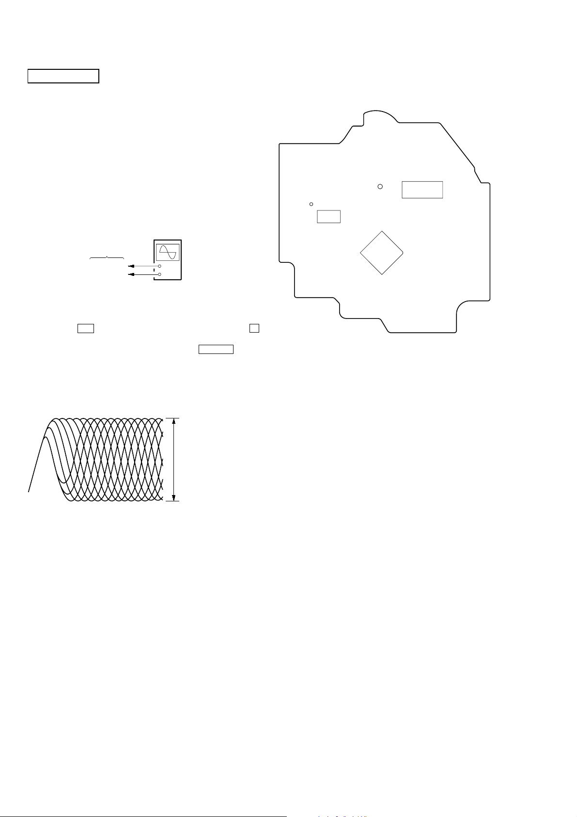
FOCUS BIAS CHECK
oscilloscope
(DC range)
BD board
TP (RFAC)
TP (VC)
Procedure :
1. Connect oscilloscope to TP (RFAC) and TP (VC) on the BD
board.
2. Press the ?/1 button to turn the power ON, and press the Z
(CD) button to open the CD disc tray.
3. Set disc (YEDS-18) on the tray and press the CD NX button
to playback.
4. Confirm that oscilloscope waveform is as shown in the figure
below. (eye pattern)
A good eye pattern means that the diamond shape ( ) in the
center of the waveform can be clearly distinguished.
+
–
s
Checking Location:
– BD BOARD (Conductor Side) –
TP
(VC)
TP
(RFAC)
IC103
IC101
IC102
VOLT/DIV: 200 m
TIME/DIV: 500 ns
level:
0.9
±
0.4 Vp-p
20
Page 21

SECTION 6
DIAGRAMS
6-1. BLOCK DIAGRAM – CD SERVO Section –
HCD-CPX1
DETECTOR
OPTICAL PICK-UP
BLOCK
(KSM-213DCP)
LASER DIODE
PD
FILTER
RF AMP,
A+3.3V
A
6
B
7
C
8
D
9
F
11
F I-V AMP
E
10
E I-V AMP
AUTOMATIC
POWER
CONTROL
LD
Q101
1
SUMMING
LD
FOCUS/TRACKING ERROR AMP
RFAC
AMP
FOCUS
ERROR AMP
RFDC
AMP
TRACKING
ERROR AMP
APC LD
AMP
SUM
RFDCO
RFDCI
TE BAL
SW
IC103
AC
4
FE
16
FEI
17
28
29
TE
18
19
12
PD
2
3
A+3.3V
EQ
IN
RFAC
VCA
RFAC
EQ
15
PWM1
PWM3
PWM2
RFAC
51
49
48
ASYMMETRY
CORRECTION
ASYI
ASYO
DIGITAL
CLV
MDP
XRST
3
26 7 8
PROCESSOR
DATA
54 56
FILO
SUBCODE
XLAT
CLOK
6
53
PCO
CLTV
DIGITAL
PLL
CPU INTERFACE
XLON
SENS
145
56 19
DIGITAL SIGNAL PROCESSOR,
DIGITAL FILTER, D/A CONVERTER
55
FILI
EFM
DEMODULATOR
SERVO AUTO
SEQUENCER
SQSO
SCOR
20
1 2
32 33
16K
RAM
SQCK
IC101 (1/2)
CORRECTOR
SERVO
INTERFACE
SCLK
COUT
9 21
D+3.3V
INTERFACE
INTERNAL BUS
ERROR
SSTP
EMPH
64 15
27
D/A
WFCK
GFS
18
When the optical
ON :
pick-up is inner
position
PCMD
BCK
LRCK
C2PO
SERIAL
INTERFACE
TO MIRR/DFCT/
FOK DETECTOR
S101
(LIMIT)
62
63
61
19
CD
MUTING
Q201
SWITCH
Q203, 204
L-CH
A
(Page 23)
R-CH
CLOCK
AIN1
71
AIN2
76
XTAO
67 66
16.9344MHz
AOUT1
AOUT2
70
77
GENERATOR
CD DIGITAL OUT
OPTICAL
IN
DIGITAL
FILTER,
NOISE SHAPER
DIGITAL
OUT
DOUT
60
PWM
&
INTEGRATOR
OPTICAL
TRANSCEIVER
IC202
BUFFER
TIMING
LOGIC
X101
XTAI
LOUT1
LOUT2
72
75
R-CH
MUTING CONTROL
2-AXIS
DEVICE
(TRACKING)
(FOCUS)
M101
(SPINDLE)
M102
(SLED)
FOCUS/TRACKING COIL DRIVE,
SPINDLE/SLED MOTOR DRIVE
IC102
16
M
15
17
M
18
12
11
13
14
MOTOR
DRIVE
MOTOR
DRIVE
COIL
DRIVE
COIL
DRIVE
MUTE
24
43
39
40
41
FE
TE
SE
23
22
SFDR
28
SRDR
29
7
6
5
4
20
TFDR
30
TRDR
31
FFDR
32
33
FRDR
FOCUS/TRACKING/SLED
RFDC
A/D
CONVERTER
PWM GENERATOR
SERVO DSP
FOCUS/TRACKING/SLED
DIGITAL SERVO
PROCESSOR
IC101 (2/2)
MIRR/DFCT/
FOK
DETECTOR
TO SERVO INTERFACE
FOK
MIRR
DFCT
24
22
23
DATA
CLOK
XLAT
PWM1
PWM2
PWM3
35
37
36
54
28
26
24
60
CD SCOR
CD SQSO
CD SENS
CD DATA
CD CLK
CD XLT
CD LD-ON
CD PWM1
CD PWM2
CD PWM3
CD XRST
CD SQCLK
SYSTEM CONTROLLER
(CD MECHANISM CONTROL)
CDM IN-SW 70
CDM OUT-SW 69
IC401 (1/4)
CDM LOAD-IN 68
CDM LOAD-OUT
78CD MUTE
IN
OUT
LOADING MOTOR
DRIVER
FIN
7
67
9
RIN
MOTOR
LOADING IN/OUT
IC201
DRIVE
S1
DETECT
OUT2
OUT1
M
M201
(LOADING)
2
4
• R-ch is omitted due to same as L-ch.
• SIGNAL PATH
: CD PLAY (ANALOG)
: CD PLAY (DIGITAL OUT)
2121
Page 22

HCD-CPX1
6-2. BLOCK DIAGRAM – TUNER/TAPE DECK Section –
L-CH
R-CH
HRPE901
(REC/PB/ERASE)
ERASE
FM 75Ω
COAXIAL
AM
RV603
REC BIAS
(R)
ANTENNA
R-CH
R-CH
FM ANT
ANT GND
AM ANT
ANT GND
BIAS OSC
T601
TUNER UNIT
RV653
REC BIAS
(L)
BIAS OSC
Q642, 643
L-CH
R-CH
ST DOUT
ST DIN
ST CLK
ST CE
ST MUTE
TUNED
STEREO
7 9
8
R-CH
BIAS
TRAP
REC BIAS
SWITCH
Q639 – 641
R-CH
DI
DO
CLK
CE
MUTING
TUNED
STEREO
REC/PB SWITCHING
IC602
A+9V
4
REC/PB
SWITCHING
Q680, 681
TUNER
L-CH
REC/PB EQ AMP, ALC
IC601
BIN (R)
37
AIN (R)
39
RECOUT (R)
10
DI
CE
DO
CLK
TUNED
STEREO
MUTING
ALC ON/OFF
11
14
EQ
R-CH
REC MUTE ON/OFF
MUTE ON/OFF
15
ALC
R-CH
EQOUT (R)
REC-IN (R)
ALC (R)
3 4
7
8
TAI (R)
RV652
REC LEVEL
(L)
MUTE
PB OUT (R)
5
(TAPE DECK BLOCK)
TC CAPM-CONT
TC TRG
59
58
CAPSTAN/REEL
MOTOR DRIVE
Q692, 694
TRIGGER
PLUNGER DRIVE
Q691, 693
MM
(CAPSTAN/REEL)
L-CH
L-CH
REC
(Page 23)
B
PB
(Page 23)
C
(Page 23)
D
• R-ch is omitted due to same as L-ch.
• SIGNAL PATH
: TUNER (FM/AM)
: TAPE PLAY
: REC
42 TC BIAS-ON
43
TC PB/REC
25
23
ST DATA IN
ST DATA OUT
27
22
ST CE
ST CLK
21
57
ST MUTE
34
ST TUNED
ST STEREO
80
TC ALC
40 41
TC REC/MUTE
TC LINE MUTE
90
38
91
SYSTEM CONTROLLER
(CD MECHANISM CONTROL)
IC401 (2/4)
TC END SW
TC PLAY SW
TC HALF/REC/SW
2222
Page 23

6-3. BLOCK DIAGRAM – MAIN Section –
HCD-CPX1
REC
(Page 22)
(Page 21)
(Page 22)
(Page 22)
MD (VIDEO)
L-CH
D
CD
L-CH
A
PB
L-CH
C
TUNER
L-CH
B
J101
L
IN
R
R-CH
R-CH : R-ch is omitted due to same as L-ch.
SIGNAL PATH
: TUNER (FM/AM)
: CD PLAY
: TAPE PLAY
: REC
: MD (VIDEO) IN
CD LCH
11
TC LCH
12
TUNER LCH
13
MD LCH
14
INPUT
SELECT
SWITCH
LCH
SELO
10 5
INTERFACE
EQ DATA
1
87 88 86
EQ DATA
CPU
EQ CLK
30
EQ CE
2
EQ CLK
LCH
IN
VOLUME
9
CONTROL
INPUT SELECT SWITCH,
EQ CE
TONE
CONTROL
ELECTRICAL VOLUME,
TONE CONTROL
IC101
LCH
OUT
MUTING
Q101
R-CH
MUTING
CONTROL SWITCH
Q121, 122
81
LINE MUTE
R-CH
A/D CONVERTER
1
LIN
2
RIN
IC603
DOUT
BCK
LRCK
PDWN15SCKI
7
CLOCK
BUFFER
IC604
X601
12.288MHz
73
P DOWN
(CD MECHANISM CONTROL)
12
11
10
SYSTEM CONTROLLER
IC401 (3/4)
18
17
16
DATA
BCK
LRCK
DIGITAL AUDIO
SIGNAL PROCESSOR
XFSIIN
SCDT
SCSHIFT
21
11
12
45
46
SC DT
SC SHIFT
IC600
SCLATCH
13
47
SC LATCH
15
49
NSPMUTE
INIT
14
48
INIT
NSP MUTE
XFSOIN
36
CLOCK
BUFFER
IC610
X602
49.152MHz
OUTL1
OUTL2
OUTR1
OUTR2
HEADPHONE AMP
IC102
HEADPHONE
MUTING
Q182
MUTING
CONTROL SWITCH
Q184, 185
R-CH
85
HP MUTE
PROTECT
SWITCH
Q696
TUNER +9V,
TC A+9V
PROTECT
DETECT
Q691, 692
RIPPLE FILTER
Q180, 181
POWER AMP
IC650
DIAGA18DIAGB
8
61
OUTA
OUTB
DIAG
9
19
R-CH
R-CH
6
INA
16
INB
ENA17ENB
7
55
ENA
2
4
41
39
R-CH
R-CH
R-CH
R-CH
50
HP DET
J801
PHONES
L
R
J701
SPEAKER
IMPEDANCE
USE 4Ω
2323
Page 24

HCD-CPX1
6-4. BLOCK DIAGRAM – DISPLAY/POWER SUPPLY Section –
LIQUID CRYSTAL
DISPLAY
LCD801
LIQUID CRYSTAL
DISPLAY DRIVER
20 – 27,
SEG0 – SEG31
30 – 41, 44 – 55
13, 16 – 18
COM0 – COM3
REMOTE CONTROL
S801 – 817
VOLUME
TREBLE
BASS
IC803
RECEIVER
IC801
ROTARY
ENCODER
RV801
ROTARY
ENCODER
RV802
ROTARY
ENCODER
RV803
SD
SCK
CS
RESET
D474, 475
LED DRIVE
LED DRIVE
LED DRIVE
LED DRIVE
LED DRIVE
RESET
SWITCH
Q501
Q801
Q802
Q803
Q804
Q805
LED DSG
LED CD
LED TC
44
83
79
84
89
12RESET
20AC CUT
1LCD ON
65CD BD-PWR
LED STANDBY
KEY1,
KEY3
100 LCD RESET
5 LCD DATA
7 LCD CLK
6 LCD CS
3 LCD CD
4 SIRCS IN/WAKE
97, 95, 94
KEY1 – KEY3
74 KEY WAKE UP
53 VOL A
52 VOL B
76 TRE A
77 TRE B
71 BASS A
72 BASS B
LED TUNER
10
9
11
1219C/D
D801
(STANDBY)
D802
DSG
D803
CD
NX
D804
TUNER
BAND
D805
TAPE
nN
RESET SIGNAL
GENERATOR
IC501
LCD+3.3V
D501
B+ SWITCH
Q431, 432
µ-COM+3.3V
+1.8V
A+3.3V,
D+3.3V
EVER
+3.3V
REGULATOR
Q301, 302
+1.8V
IC618
CD ON
SWITCH
RDS+3.3V
D402
D404
D401
D403
D301
D303
D302
+4V
REGULATOR
IC991
+4V
REGULATOR
IC301
RECT
D992 – 995
TC M+11.5V
T991
SUB POWER
TRANSFORMER
SYSTEM CONTROLLER
(CD MECHANISM CONTROL)
IC401 (4/4)
PWR RELAY
XCOUT
XIN
XOUT
X401
16MHz
1513
X402
32.768kHz
1011
XCIN
A+5V,
D+5V
D806 – 808
(LCD BACK LIGHT)
51LED BL
82
B+ SWITCH
Q433, 434
D+6.2V
M+7V
TUNER +9V,
TC A+9V
D304
+5V
REGULATOR
IC302
+7V
REGULATOR
IC303
+9V
REGULATOR
IC304
SWITCHING
+28V
POWER ON/OFF
RELAY DRIVE
Q991
POWER ON/OFF
RELAY DRIVE
Q990
(Singapore, Korean, Australian)
REGULATOR
RY991
RY990
(AC IN)
2424
Page 25

HCD-CPX1
AMP board
LCD board
BACK LIGHT board
SWITCH board
HP board
MAIN board
TUNER UNIT
SUB POWER board
SP OUT board
SWITCHING REGULATOR
6-5. NOTE FOR PRINTED WIRING BOARDS AND SCHEMATIC DIAGRAMS
Note on Printed Wiring Board:
• X : parts extracted from the component side.
• Y : parts extracted from the conductor side.
• W : indicates side identified with part number.
f
•
• : Pattern from the side which enables seeing.
(The other layers' patterns are not indicated.)
Caution:
Pattern face side: Parts on the pattern face side seen from
(Conductor Side) the pattern face are indicated.
Parts face side: Parts on the parts face side seen from
(Component Side) the parts face are indicated.
• Indication of transistor.
: internal component.
C
Q
B
E
B
B
These are omitted.
Q
CE
Q
CE
These are omitted.
These are omitted.
Note on Schematic Diagram:
• All capacitors are in µF unless otherwise noted. pF: µµF
50 WV or less are not indicated except for electrolytics
and tantalums.
• All resistors are in Ω and 1/
specified.
f
•
• 5 : fusible resistor.
• C : panel designation.
• A : B+ Line.
• H : adjustment for repair.
•Voltages and waveforms are dc with respect to ground
•Voltages are taken with a V OM (Input impedance 10 MΩ).
•Waveforms are taken with a oscilloscope.
• Circled numbers refer to waveforms.
• Signal path.
•Abbreviation
: internal component.
Note:
The components identified by mark 0 or dotted
line with mark 0 are critical for safety.
Replace only with part
number specified.
under no-signal (detuned) conditions.
no mark : TUNER (FM/AM)
(): CD PLAY
[]: TAPE PLAY
〈〈 〉〉 : REC
Voltage variations may be noted due to normal production tolerances.
Voltage variations may be noted due to normal production tolerances.
F : TUNER (FM/AM)
J : CD PLAY (ANALOG)
c : CD PLAY (DIGITAL OUT)
E : TAPE PLAY
a : REC
j : MD (VIDEO) IN
AUS: Australian model
CND : Canadian model
KR : Korean model
SP : Singapore model
: Impossible to measure
∗
4
Note:
Les composants identifiés par
une marque 0 sont critiques
pour la sécurité.
Ne les remplacer que par une
pièce portant le numéro
spécifié.
• Circuit Boards Location
W or less unless otherwise
TC board
LOADING board
BD board
2525
Page 26

HCD-CPX1
6-6. PRINTED WIRING BOARD – BD Board – • See page 25 for Circuit Boards Location. :Uses unleaded solder.
S101
C159
R159
IC102
JW633
C172
R172
C112
(LIMIT)
C153
R173
JW632
C182
C125
C114
C163
R183
JW621
JW600
JW601
JW628
JW629
R118
JW631
JW630
R117
C181
JW636
JW637
OPTICAL
PICK-UP
BLOCK
(KSM-213DCP)
BD BOARD
JW609
C143
JW611
JW610
JW620
JW622
C192
JW626
R195
R192
R191
JW647
JW627
C130
JW625
C145
C146
R122
JW624
JW641
C110
C194
R101
C193
R148
(RFAC)
JW623
R196
C184
C185
C118
C117
TP
R111
C133
R103
C104
JW646
JR101
E
Q101
C116
C101
C196
JW612
JW619
R151
R120
R194
C183
JW618
R143
IC103
C102
R102
C103
JW644
C165
C131
JW645
R114
R104
C124
JW613
R193
C123
C111
JW648
JW608
JW617
C197
R150
C150
JW643
ON : WHEN THE OPTICAL PICK-UP
IS INNER POSITION
R158
S101
28 22 21 15
17 814
JW603
JW602
JW607
CN102
JW616
R147
C140
JW606
JW614
JW615
R144
JW605
M
(VC)
JW634
M101
(SPINDLE)
R197
R162
TP
JW604
2021
IC101
40
41
R123
R124
R107
R108 FB103
R109
C108
R106
C109
R131
JW640
6160
C168
C167
JW639
1
80
R181
R182
X101
R171
R119
C171
JW635
C121
C198
C122
C126
C127
RN101
M
M102
(SLED)
CN101
A
MAIN
BOARD
CN202
(Page 31)
1-686-781-11(11)
R116
C162
FB101
C191
JW638
2626
Page 27

6-7. SCHEMATIC DIAGRAM – BD Board – • See page 30 for Waveforms. • See page 40 for IC Block Diagrams.
R107
VSS
VDD
XRST
SQCK
1k
R117
4
D
C109 C111 R109
1500p 100p 1M
R108C108
3.3k0.1
R106
1k
10k
FILI
PCO
AVDD3
DIGITAL SIGNAL PROCESSOR,
DIGITAL SERVO PROCESSOR,
DIGITAL FILTER,D/A CONVERTER
XLAT
DATA
SYSM
5
6
D
D
C116
C146
C130
C165C183 C184
0.10.068 0.022
C124
0.47
C123
0.01
R124
100k
33k
R123
10k
R104
FILO
CLTV
SENS
CLOK
8
7
D
D
ASYI
BIAS
RFAC
AVSS3
IC101
CXD3017Q
LK
VDD
SC
9
D
IGEN
ASYO
AVSSO
AVDDO
F
N
FCK
XUG
W
XLO
SPOB
SPOA
ATSK
RFCK
3300p
0.1
0.1
C110
TE
CE
ADIO
RFDC
TRDR
SRDR
MIRR
R
K
CO
S
C2PO
GFS
XPC
M3M0M1
JR101
100
0
16V
SE
FE
VC
XTSL
TES1
TEST
VSS
FRDR
FFDR
TFDR
SFDR
SSTP
MDP
LOCK
FOK
DFCT
COUT
S101
ON:WHEN THE OPTICAL PICK-UP
(LIMIT)
IS INNER POSITION.
(Page
33)
CN101
21P
PWM3
PWM2
PWM1
D+3.3V(SW)
DOUT
DGND
L-CH
AGND
R-CH
A+3.3V(SW)
XRST
DATA
XLAT
CLK
LDON
SQSO
SENS
SQCK
SCOR
MGND
M+7V
C198
100
16V
C112
1
C162
100
16V
FB101
R116
10
0
X101
16.9344MHz
C168
24p
C167
1.8k
R119
C171
680p
R173
22k
D2
D3
R183
22k
C181
680p
D1
D2
D3
D4
D5
C125
D6
0.1
D7
100
RN101
D8
100
D9
R118
27p
R171R172
22k22k
C172
100p
C182
100p
R182 R181
22k 22k
C163
100
16V
FB103
C114
0
0.1
C122 C191
100
16V
C121
0.1
100
16V
LRCK
PCMD
BCK
EMPH
XVDD
XTAI
XTAO
XVSS
AVDD1
AOUT1
AIN1
LOUT1
AVSS1
AVSS2
LOUT2
AIN2
AOUT2
AVDD2
RMUT
LMUT
C185
2.2
1
D
R131
220
DOUT
SQSO
9
D
DGND
HCD-CPX1
R196
2.2k
R195
330k
R194
68k
C193
C194
100
0.1
16V
TP
(RFAC)
C192
100
16V
R103
15k
C101
3300p
C103
C145
470p
0.1
R102
C104
100k
470p
C102
0.1
C153
0.1
R197
1k
C126
0.1
C127
100
16V
C133R111
33p120k
R191
33k
R192
33k
R151
C150R120 R101
0.115k 1k
120k
R114R193
390k150k
R147
3.9k
R150
10k
FOCUS/TRACKING ERROR AMP
TT+
F+
IC103
CXA2647N-T4
RFACFE
DVC
FEI
DVCC
TE
SW
TE_BAL
CE
CEI
VCC
RFG
BST
VFC
GND
RFC
AC_SUM
VC
EQ_IN
RFDCO
PD
RFDCI
DC_OFST
LD
RF AMP,
IC102
BA5947FP
FOCUS/TRACKING COIL DRIVE,
SPINDLE/SLED MOTOR DRIVE
R143
R158
R144
22k
D4
18k
18k
Q101
2SB970
AUTOMATIC
POWER
CONTROL
F
E
D
C
B
A
C197
0.1
C131
C196
100
0.1
16V
C118
1000p
C117
100
16V
R122 R148
100k 3.3
R162
4.7k
C159 R159
6800p 22 k
TP
(VC)
E6
E1
E2
E5
E4
E3
E7
E8
0.1
C143
CN102
C140
16P
1
VC
VCC
E1
E
E2
D
E3
A
E4
B
E5
C
E6
F
GND
E7
LD
VR
E8
PD
F+
F+
T+
T+
T-
T-
F-
F-
M102
(SLED)
M101
(SPINDLE)
The components identified by mark 0 or dotted
line with mark 0 are critical for safety.
Replace only with part number specified.
Les composants identifiés par une marque 0 sont
critiques pour la sécurité. Ne les remplacer que
par une pièce portant le numéro spécifié.
2727
Page 28

HCD-CPX1
6-8. PRINTED WIRING BOARD – TC Board – • See page 25 for Circuit Boards Location. :Uses unleaded solder.
• Semiconductor
Location
Ref. No. Location
D681 C-4
IC601 F-7
IC602 H-6
Q639 D-4
Q640 D-5
Q641 E-5
Q642 H-2
Q643 G-3
Q680 F-5
Q681 F-5
Q691 B-6
Q692 B-5
Q693 C-3
Q694 C-5
1 2 3 4 5 6 7 8
C608
B
JW631
R631
2021
MAIN BOARD
(Page 31)
JW633
C632
1
C651
C663
JW636
18
CN211
JW624
JW623
JW625
11
10
CN603
R630
C630
R651
C660
R635
JW604
R657
R660
C634
C656
JW638
R652
R653
JW600
R654
C655
R659
C657
C654
C652
C664
R632
R633
C633
JW634
R661
RV652
C658
R655
R656
TAPE DECK BLOCK
A
SUPPLIED WITH THE
ASSEMBLED BLOCK
CN602
B
Q693
C
D
JW635
E
C681
D681
R683
E
Q639
R647
R648
C640
JW617
C639
E
C614
F
R644
R643
G
JW615
C641
Q642
Q643
E
C646
E
R645
C643 C645
C644
R646
H
T601
JW616
RV603
C612
RV653
C662
R641
R607
JR602
C610
L601
C611
TC BOARD
JW637
JW640
E
Q694
C647
E
Q640
R642
Q641
E
R605
E
R610
E
L651
C661
R681
R682
L641
R606
Q680
JW627
Q681
R695
R694
R690
E
Q692
R687
JW612
JW621
JW609
C635
R686
R604
C605
R689
E
R685
C602
C601
Q691
R684
RV602
R603
R680
R602
R601
R688
R691
C604
JW632
R609
JW610
30
31
R611
C607
JW628
C606
IC601
40
R692
L640
R693
R640
JW626
IC602
19
JW608
JW602
NO601
JW613
C613
JW630
JW607
I
J
C642
HEAD
RELAY
BOARD
1-686-408-
HRPE901
(REC/PB/ERASE)
L-CH
R-CH
ERASE
11
(21)
2828
Page 29

6-9. SCHEMATIC DIAGRAM – TC Board – • See page 30 for Waveform.
HCD-CPX1
ERASE
REC/PB SWITCHING
IC602
.
1
1
D
T
.P
N
.R
W
S
HRPE901
(REC/PB/ERASE)
L-CH
R-CH
L-PB
L-REC
R-REC
R-PB
GND
E-HOT
(CHASSIS)
NO601
L-PB
GND
L-REC
R-REC
GND
R-PB
GND
E-HOT
8P
0
JW630
N
G
O
W
S
C
2
C
D
N
G
C642
0.01
100V
D
C
.P
N
V
G
W
S
C613
390p
RV653RV603
220k220k
C662C612
27p27p
T601
BIAS OSC
BA3126N
2
.R
W
S
Q681
R680
DTA124ESA
4.7k
Q680,681
REC/PB
SWITCH
Q680
C663
DTC114ESA-TP
390p
C611
120p
L601
27mH
JR602
0
L651
27mH
C661 R660
120p 8.2k
R606
2.2k
R607
R610
10k
8.2k
C610
330p
C660
330p
Q642
2SC2001
R644R643
5.65.6
R605C614
47k0.01
C664
R655
0.01
47k
R657
10k
R656
2.2k
Q642,643
BIAS OSC
Q643
2SC2001
C601
47
16V
C635
1
50V
C651
47
16V
0.0068
0.0068
18k
18k
0.015
R645
C643
0.018
C644
C645
R646
C646
Q641
2SD1387-34-TP
C641
2.2
50V
R641
6.8k
R602 R604 C607 R609
4.7k 10k 470p 2.2k
50V
0.1
4.7k
3.3k
0.01
R603
C602
C652
0.01
4.7k
R653
R651
3.3k
C639
10
50V
R601
REC/PB EQ AMP,ALC
HA12236
0.1
C654
R652
4.7k
R642
2.2k
C640
47
16V
C604
50V
10
C655
10
C605
1
50V
Q639-641
REC BIAS
DTC114ESA-TP
SWITCH
Q640
CN602
RV602
22k
R611
22k
50V
1
C606
C608
2.2
50V
Q694
2SB1068
R695
10k
R631
22k
R630C632
1M10 50V
C630IC601
100
16V
R635
100
C633
10
50V
C634
10
RV652
R659C657R654
2.2k470p10k
Q639
2SA1175
22k
R647R648
22k2.2
C658C656
2.2
50V
50V
R633R632
10k1k
R661
22k
L640
L641
R640
C647
10
50V
10k
R694
22k
R693
47k
R688
4.7k
R689
4.7k
R690
4.7k
R691
10k
R692
4.7k
R687
47k
R684R685R686
3.3k3.3k3.3k
Q692,694
CAPSTAN/REEL
MOTOR DRIVE
D681
1SS355TE
Q692 Q691
DTC114EKA DTC114EKA
C681 R683
0.0047 680
R682
2.2k
TRIGGER PLUNGER
2SB1116
Q691,693
DRIVE
Q693
R681
2.2k
PLAY SW
END SW
M+11.5V
TC TRIG
TC CAPM
TC END-SW
TC HALF-REC
TC PLAY
BIAS-ON/OFF
LINE-MUTE
REC-MUTE
M+10V
TRGM+
REC/PB
R REC
MGND
MGND
REC-R
REC-L
A-GND
8P
F REC
PACK
CN603
19P
+3.3V
ALC
PB-R
PB-L
A+9V
TAPE DECK BLOCK
SUPPLIED WITH
THE ASSEMBLED
(Page 32)
BLOCK
The components identified by mark 0 or dotted
line with mark 0 are critical for safety.
Replace only with part number specified.
Les composants identifiés par une marque 0 sont
critiques pour la sécurité. Ne les remplacer que
par une pièce portant le numéro spécifié.
2929
Page 30

HCD-CPX1
p
p
p
p
p
p
p
p
p
• Wavef orms
– BD Board –
1 IC103 qg (RFAC) (CD play mode)
5 IC101 rd (RFDC) (CD play mode)
– TC Board – – MAIN Board –
qa Q642, 643 (Collector) (REC mode)
wa IC401 qa (XCOUT)
– AMP Board –
ea IC603 q; (LRCK)
– LCD Board –
ra IC803 3 (OSC2)
2 IC101 wh (MDP) (CD play mode)
µ
s
7.6
3 IC101 el (FE) (CD play mode)
0.9 ± 0.4 Vp-
1.7 Vp-p
6 IC101 yj (XTAO)
59.1 ns
0.8 ± 0.4 Vp-
1.9 Vp-
12.8 µs
12 Vp-
30.5 µs
ws IC501 qd (X-OUT)
62.5 ns
2.2 Vp-
2 Vp-p
20.7 µs
es IC603 qa (BCK)
326 ns
ed IC604 6
3.3 Vp-
3.4 Vp-
3.6 Vp-
27.3 µs
4 IC101 ra (TE) (CD play mode)
0.4 Vp-
0.3 Vp-p
2 Vp-p
81.4 ns
3030
Page 31

6-10. PRINTED WIRING BOARDS – LOADING/MAIN Boards – • See page 25 for Circuit Boards Location. :Uses unleaded solder.
HCD-CPX1
1 2 3 4 5 6 7 8 9 10 11 12
TC BOARD
JW152
R124
C185
JW200
JW163
D301
CN603
JW160
JW410
R123
JW399
C154
C104
JW162
CN301
C122
C182
JW199
(Page 28)
D303
D302
1
2
JW150
JW144
C121
R121
IC102
JW137
Q181
R182
C183
JW396
C313
C312
C315
C314
JW148
JW147
JW145
C171
R172
R122
C172
C181
E
R181
R183
EE
Q201
Q202
R174
IC301
IC302
JW311
JW391
R171
C173
JW136
R222
R221
CN211
JW313
JW312
R173
3
1
JW146
R180
JW139
JW135
3
1
JW390
C180
JW140
JW134
C301
Q180
JW138
10
E
C105
Q203
JW395
11
JW314
JW394
IC304
JW105
IC303
JW389
JW15
JW16
JW370
JW118
JW392
C103
C107
C108
C109
C110
R103
C111
Q101
E
Q204
EE
JW130
JW128
JW129
JWS001
C318
1
3
C319
C316
1
3
C317
JW17
15 16
JW112
JW387
JW106
JW388
JW109
JW372
JW120
JW386
JW119
JW373
IC101
C132
130
JW124
C131
R104
R133
R132
R131
JW133
R105
R106
JWS002
JW132
JW374
Q122
JW122
E
E
Q121
C209
JW385
C133
Q151
FB121
R101
R102
C101
C102
JW113
JW114
JW121
C159
C160
R157
JW125
EP101
(CHASSIS)
R153
JW126
FB123
JW103
JW104
C158
R154
R155
E
C153
C157
C161
IC202
C210
C141
FB122
R151
R152
C151
C152
JW111
JW393
C155
3
1
1-686-797-
R
L
C
SWITCHING
REGULATOR
(Page 38)
IC202
CD DIGITAL OUT
OPTICAL
21
J101
MD (VIDEO)
IN
MAIN BOARD
R440
JW182
R506
JW253
R437
R432
R428
R552
D503
D502
JW369
31
JW255
R253 R254
R251
JW213
CN401
JW254
CN101
FB102
JW212
R425
D501
R482
R210
R420
1
3
JW368
JW194
JW195
R252
R491
JW171
JW170
JW174
IC501
R502
R501
R505
D403
D404
D401
D402
JW187
FB101
C252
C251
JW172
JW175
C501
JW384
D304
R490
JW169
JW173
JW176
JW371
JW168
JW205
JW406
JW206
JW167
JW177
JW185
JW186
JW189
JW183
JW184
JW190
JW191
JW192
JW193
LP101
JW166
JW207
CN221
JW155JW156
Q185
JW204
R413
JW248
JW247
JW246
JW245
JW244
JW239
JW238
JW237
C232
R409
R406
JW267
JW220
FB205
FB206
R458
JW262
JW250
C222
JW219
C402
JW362
C407
R459
31
30
C405
C406
R411
X402
JW261
JW249
JW218
JW364
R417
X401
JW260
C225
C228
JW359
JW217
R430
R421
JW361
JW360
JW358
JW259
JW251
FB204
R441
R438
R426
R423
C401
JW407
C229
JW214
R447
R445
R443
JW363
R448 R449
R435
R434
R429
R422
R419
C503
D504
R504
JW365
JW258
JW257
JW211
JW215
C226
C227
FB202
FB203
CN202
A
BD BOARD
CN101
(Page 26)
R427
E
JW366
R553
JW209
C224
R446
R442
R436
R433
R424
C502
R503
Q501
JW367
JW256
JW252
FB103
C221
R444
FB201
R456
JW382
4
1
C204
R555
JW336
JW335
R477
JW305
JW323
JW322
JW321
JW320
JW319
JW318
JW325
JW324
JW317
C432
R489
JW383
9
JW303
C203
1
IC201
R471
JW280
CN402
JW337
R565
CN403
R557
R480
JW279
C202
R556
R202
R201
JW379
JW302
JW309
R476
R474
JW333
JW332
JW308
JW278
Q433
C201
R460
R457
R567
JW277
JW296
R566
R472
R554
R452
R453
JW276
JW316
E
Q434
JW298
C223
R479
JW347
E
Q432
C431
JW299
JW300
JW301
JW304
R461
D474
D475
JW275
Q431
E
JW408
JW409
JW353
JW349
JW350
JW346
JW345
R541 R543
(US, CND)
JW342
JW338
JW274
JW272
JW273
E
C433
JW295
JW294
JW228
JW227
JW310
JW293
JW292
JW291
JW282
JW286
JW285
JW287
JW348
JW344
R544
JW341
JW340
JW339
JW271
C231
JW352
C404
80
81
JW343
R494
R563
R562
JW270
JW288
JW229
EP201
(CHASSIS)
JW269
JW289
JW226
JW351
R564
JW268
JW290
IC401
R495
R497
JW263
JW225
JW266
JW224
R500
R450
51
1100
R401
JW265
JW223
R551
R403
JW357
JW355
JW236
JW235
JW234
JW233
JW232
JW231
JW230
JW222
50
R405
R404
R407
JW356
JW354
JW264
JW243
JW242
JW241
JW240
JW221
JW376
R454
JW330
JW329
JW328
JW307
JW306
R559
R558
R560
R451
R455
R561
R473
A
B
C
D
H
SUB POWER
BOARD
NO992
(Page 38)
E
F
(Page 34)
(Page 36)
SWITCH
(Page 36)
G
H
(Page 38)
LOADING BOARD
CN151
I
S1
LOADING IN/OUT
DETECT
OUT
IN
M201
(LOADING)
D
AMP
BOARD
CN601
E
LCD
BOARD
CN802
F
BOARD
CN801
G
HP
BOARD
NO805
1-674-336-
JW315
R484
R483
JW380
JW381
CN102
R469
R470
C205
1
5
CN201
12
(12)
J
B
C156
C106
JW165
JW164
Q301
E
Q302
E
C321
JW161
JW153
JW154
JW158
JW157
JW159
R125
R126
E
C124
Q182
R176
R175
C174
R184
R185
E
Q183
Q184
EE
JW201
JW377
JW397
JW398
JW400
TUNER UNIT
SUPPLIED WITH THE
ASSEMBLED BLOCK
FM 75Ω
COAXIAL
AM
ANTENNA
C123
• Semiconductor
Location
Ref. No. Location
D301 C-8
D302 C-8
D303 B-8
D304 F-7
D401 C-6
D402 D-6
D403 C-6
D404 C-6
D474 C-4
D475 C-4
D501 C-6
D502 C-6
D503 C-6
D504 C-6
IC101 F-10
IC102 F-8
IC201 H-3
IC202 H-11
IC301 C-9
IC302 C-9
IC303 C-10
IC304 C-10
IC401 B-5
IC501 C-6
Q101 G-10
Q121 H-10
Q122 H-10
Q151 H-11
Q180 F-9
Q181 G-8
Q182 G-8
Q183 G-8
Q184 G-8
Q185 G-7
Q201 H-8
Q202 H-9
Q203 H-9
Q204 H-10
Q301 C-8
Q302 C-8
Q431 F-4
Q432 E-4
Q433 F-4
Q434 F-4
Q501 C-6
3131
Page 32

HCD-CPX1
6-11. SCHEMATIC DIAGRAM – MAIN Board (1/2) – • See page 40 for IC Block Diagram.
(1/2)
CN221
19P
M+11.5V
MGND
ANTENNA
FM 75Ω
COAXIAL
TC TRIG
TC CAPM
+3.3V
TC END-SW
TC HALF-REC
TC PLAY
BIAS-ON/OFF
REC/PB
LINE-MUTE
REC-MUTE
(Page 29)
TUNER UNIT
SUPPLIED WITH
THE ASSEMBLED
MD(VIDEO)
BLOCK
IN
L
R
AM
ALC
PB-R
REC-R
PB-L
REC-L
A-GND
A+9V
CN211
11P
ST CLK
ST DOUT
ST DIN
ST CE
+9V
TUNED
STEREO
L OUT
AGND
R OUT
ST MUTE
J101
2P
C141
1000p
CN301
2P
GND
+10-12V
(Page 39)
(CHASSIS)
(Page 35)
CN101
21P
A+5V
AGND
L-IN
AGND
R-IN
P-DOWN
DGND
D+3.3V
INIT
NSP MUTE
DGND
SC LATCH
SC SHIFT
SCDT
D+5V
DGND
D+6.2V
DGND
ENA
SP-RELAY
DIAGNOSTIC
27
25
23
22
57
34
Z5
Z6
21
FB121 R101
0 10k
FB123
0
FB122
0
EP101
FB102
FB103
58
59
R103
90
91
38
42
43
40
41
80
Z1
Z2
Z3
Z4
C101
R102
220p
8.2k
C151R152
220p
8.2k
R151
10k
73
FB101
49
48
47
46
45
55
61
5
3
Z
Z
50V
50V
1
1
1
50V 10
C104
C103
C
H
H
N
C
C
L
L
D
ER
M
N
TU
H
C
R
H
C
R
E
R
N
D
C
U
N
M
T
50V
C152
50V
50V
1
1
1
C154
C153
1
6
Z
Z
R154
1k
R155
10k
R105
10k
C171
10
R171
50V
1k
C108
4
Z
50V
1
C105
H
O
H
C
C
EL
L
L
S
C
T
H
CD
C
L
LO
E
H
H
C
C
S
R
H
R
C
D
C
T
C
R
50V
1
C155
2
Z
Q151
2SC3624
MUTING
Q101
2SC3624
MUTING
R122 R172 R183 R181
100k 100k 10k 2.2k
C121
R121
1k1050V 10 50V 4.7k
C156
50V
0.0027
C106C102
3.9k
1
50V
C109
50V
1
C107
E
R
IN
H
L T
LC
E
IN
R
H
C
T
R
R
50V
C159
C157
1
1
R104
1k
C111
50V
C110
0.12
0.12
T
2
T
1
S
S
A
B
L
1
S
S
A
B
R
0.12
R153C158
3.9k0.0027
R157
10k
R106
10k
C183
100
10V
S
U
SS
O
TE
A
H
L B
LC
T
2
U
S
S
O
A
H
C
B
C
N
R
R
C160
0.12
C161
10
50V
C133
100
10V
MUTING CONTROL
C123 R123
HEADPHONE AMP
NJM4580MD
C173
R173 R174
10 50V
4.7k 22k
6
8
R133 R132
100 100
S
S
V
F
E
R
V
Q121,122
SWITCH
Q122
DTC114EKA
RIPPLE
FILTER
IC102
1000p
E
C
EQ
D
D
V
C122
7
8
C132
0.1
DTA114EKA
C172
1000p
GND
A
T
A
D
Q
E
IC101
LC75342
K
L
C
Q
E
INPUT SELECT SWITCH,
ELECTRICAL VOLUME,
TONE CONTROL
C131
100
10V
Q121
C182
R182
1
2.7k
50V
R124
VCC
A1
A2
A3
8
8
8
R131
100
7
Q201
2SC3624
MUTING
Q202
2SC3624
MUTING
Q203
DTA114EKA
Q203,204
MUTING CONTROL
SWITCH
Q204
DTC114EKA
R221
10k
R222
10k
TA7809S
C319
470
10V
C315
100
10V
+4V REGULATOR
IC304
BA09T (US,CND)
(SP,KR,AUS)
OI
G
+5V REGULATOR
IC302
TA7805S
OI
G
C318
0.1
50V
0.1
50V
C301 C312
4700
16V
C316C314
0.1
50V
0.1
50V
+4V REGULATOR
IC301
µPC3504AHF
OI
G
+7V REGULATOR
IC303
TA7807S
OI
G
D302
1SS355TE
C317
470
10V
D301 D303
10EBD40 10EBD40
C313
470
10V
Q301,302
CD ON SWITCH
D304
10EBD40
Q301
RT1P137S
DTC114EKA
Q302
C321
470
10V
A4
A5
(Page 33)
A6
Q180Q181
2SC36242SC3624
RIPPLE
FILTER
Q184,185
SWITCH
C180
220
10V
DTA114EKA
R180
4.7k
Q185
DTC114EKA
C185
1
50V
Q184
R185 R184 R125
1k 1k 47
Q183 Q182
2SC3624 2SC3624
HEADPHONE
MUTING
HEADPHONE
MUTING
R126R176
100k100k
A7
A8
A9
A10
A11
A12
A13
A14
A15
C181
100
10V
22k
C124
220
10V
MUTING CONTROL
C174
220
R175
10V
47
3232
Page 33

6-12. SCHEMATIC DIAGRAM – LOADING/MAIN (2/2) Boards – • See page 30 for Waveforms. • See page 40 for IC Block Diagram.
HCD-CPX1
(Page 32)
(2/2)
A1
A2
A3
A4
8
A5
8
4
5
5
5
2
3
5
5
100
100
R453
L B
VO
MUTETC REC/
LK
IIC C
IC501
M62703SL
100
R454
R455
N
L A
-O
O
V
LD
CD
1
M
W
P
T CLK
D
S
C
150k
68k
100
R426
R428
R427
7
8
6
2
2
2
OI
G
RESET SIGNAL GENERATOR
10k
R556
10k
R554
10k
7
5
R450
R449
49
R448
48
R447
47
R446
46
R445
45
R444
44
100
R443
43
100
R442
42
100
R441
41
40
38
100
R437
37
36
35
34
33
32
A6
A7
A8
A9
A10
A11
A12
A13
A14
A15
100
R436
100
R435
100
R434
100
R433
100
R432
R553
10k
D404
1SS355TE
D402
1SS355TE
D403
1SS355TE
D401
1SS355TE
R505
4.7k
D501 C503 R503
1SS355TE 0.1 47k
R555
10k
R557
100
100
R451
R452
LED BL
100
100
100
100
100
100
100
R438R440
100100
HP DET
INIT
NSP MUTE
SC LATCH
SC SHIFT
SC DT
LED STANDBY
PB/RECTC
TC BIAS-ON
TC LINE MUTE
32K OUT
TC PLAY SW
CD CLK
CD XLT
CD DATA
ST STEREO
CD SQCLK
CD SQSO
NO USE
IIC DATA
R430
10k
R429
10k
R501
220
C501
R502
10
10k
50V
9
6
0
1
5
5
5
6
6
100
100
100
100
100
10k
R456
R458
R459
R460
R461
R567
100
R457
A
S
ED
EN
EN
N
S
D
C
ST TU
3
2
M
M
W
W
ATA IN
P
P
T D
D
S
CD
C
2.7k
100
R424
R425
4
5
2
2
C404
0.1
T
T
N
O
-C
M
AP
C
TC
T CE
S
100
R422
2
2
1SS355TE1SS355TE
S
XR
CD
TE
U
ST M
4.7k
100
R420
R421
1
2
C
IAG
VC
D
(CD MECHANISM CONTROL)
R
T
CO
S
CU
D
AC
C
0
100
R552
R419
9
1
G
TR
TC
T
U
TA O
A
T D
S
100
R423
3
2
D503D502
R566
10k
R565
10k
R
SS
V
-PW
FT TEST
BD
SO
CD
SYSTEM CONTROLLER
IC401
M30622MGN-B08FP
LK
C
1
S
M
D
CC
V
N
R
R417
10k
R413
0
C502
0.1
Y
ELA
P R
S
XIN
16MHz
7
8
6
6
T
U
-IN
D
-O
A
D
A
LO
M
LO
D
M
C
CD
T
U
S
O
X
VS
X401
0.1
C405
9
6
100
R469
W
T-S
U
O
M
D
C
ET
ES
R
X402
0
7
100
R470
-SW
IN
M
CD
T
U
O
XC
R411
330k
C407
32.768KHz
3
7
1
2
R559
7
100
R471
S A
AS
B
IN
XC
R409
10k
22p
D504R504
1SS355TE47k
6
7
10k
7
100
R558
100
100
10k
R476
R473
R472
P
N
B
S
U
W
E
O
AS
D
B
AK
P
W
EY
K
K
L
S
S
C
C
VS
TE
Y
N
CD
B
LCD
C
L
100
100
100
R407
R406
R405
15p
5
6
7
C406
R506
10k
Q501
2SC2785
RESET
SWITCH
0
7
8
R560
10k
9
R561
7
7
10k
7
R474 D474
100
R479
ED
L
PWR RELAY
LED TUNER
A
AT
D
S
D
R
0
R551
100
R480
TC ALC
D
C
LINE MUTE
LED DSG
HP MUTE
EQ DATA
EQ CLK
LED TC
TC END SW
MODEL
N
O
D
LC
100
R401
1
RESET
EQ CE
DEST
KEY3
KEY2
AVSS
KEY1
VREF
AVCC
LCD
C401
1000
6.3V
C402
1M 1SS355TE
D475
1SS355TE
R541
0.1
R482
100
R483
100
R484
100
86
87
88
R489
100
R490
100
R491
R543
R544
(US,CND)
100
∗
2.2k
0
∗
0
10k
R563
R543
(US,CND)4.7k
(SP,KR,AUS)
83
84
67
89
90
91
R494
10
94
95
R495
10
100
R500
100
97
R497
10
10k
10k
R562
R564
4
68
E A
TR
TA
A
D
LCD
100
R477
E B
TR
E
K
A
/W
IN
S
C
IR
S
100
R404
E
T
U
M
D
C
TC HALF/REC/SW
CD
D
LC
100
R403
3
1
C201
100
10V
Q433
DTA123YKA
B+ SWITCH
Q434
DTC114EKA
B+ SWITCH
DTA114EKA
B+ SWITCH
DTC114EKA
B+ SWITCH
LOADING MOTOR DRIVE
IC201
BA6956N
FIN
GND
RIN
Q431
Q432
RNF
OUT1
VM
VCC
R201
470
C202 R202
0.1 1k
C432
10
50V
C431
10
50V
VREF
OUT2
C203
0.1
100
7
5
6
3
89
84
4
44
83
94
95
97
72
71
77
76
52
53
79
69
70
C205 C204
0.1 0.1
C231
100p
C433
0.1
C228
0.1
C227
0.1
BACK LIGHT +7V
LED GND
LCD RESET
LCD CLK
LCD DATA
LCD CS
LCD C/D
+3.3V(EVER)
LED GND
LED TAPE
+3.3V(EVER)
LED TUNER
D-GND
LED STANDBY
LED DSG
BASS-B
BASS-A
LED CD
OUT SW
C223
100
10V
10V
6.3V
100
0.1
0.1
470
C222
C225
C224
C221
R254
100k
R253
100k
0.1
0.1
C229
C226
SIRCS
TRE-B
TRE-A
VOL-B
VOL-A
IN SW
(Page 37)
GND
CN403
9P
CN402
19P
+7V
KEY3
KEY2
KEY1
(Page 37)
CN201
5P
OUT2
OUT1
GND
FB206
FB205
FB204
R252
1k
R251
1k
CN151
5P
OUT2
OUT1
OUT SW
GND
IN SW
0
19
JWS002
FB201
FB203
FB202
C232
100p
33
56
32
54
37
36
35
60
28
26
24
R210
100
C209
C210
100
0.1
10V
0
C252
2.2
50V
C251
2.2
50V
LOADING IN/OUT
EP201
OPTICAL
TRANSCEIVER
DETECT
IC202
TOTX141
OUT
IN
S1
A+3.3V(SW)
D+3.3V(SW)
MGND
PWM1
PWM2
PWM3
HP DET
HP GND
SUB.GND
+4V(EVER)
RELAY ON
M+7V
SCOR
SQCK
SENS
SQSO
LDON
XRST
AGND
DGND
DOUT
OUT
+5V
GND
CN202
XLAT
DATA
R-CH
L-CH
CN102
HP R
HP L
CN401
21P
CLK
4P
3P
(LOADING)
(Page 27)
(CHASSIS)
(Page 39)
(Page 39)
CD DIGITAL OUT
OPTICAL
M201
3333
Page 34

HCD-CPX1
6-13. PRINTED WIRING BOARD – AMP Board – • See page 25 for Circuit Boards Location. :Uses unleaded solder.
1 2 3 4 5 6 7 8 9 10 11 12 13 14 15 16
(COMPONENT SIDE)
C690
R610
R609
D662
(CHASSIS)
AMP BOARD
A
AMP BOARD
B
C622
C604
C634
C635
C633
R605
IC600
R618
C607
IC603
R642
R640
C636
135
IC610
C612
IC604
R614 R615
R641
C650
D652
R619
X602
4
R620
X601
Q692
D682
C668
D672
C670
C
D
R607
E
F
G
C692
EE
Q693
EE
C693
R695
R694
R661
NO691
2
1
5
1
CN600
Q691
Q694
R696
R692
J
SP OUT
BOARD
CN701
(Page 38)
L
SWITCHING
REGULATOR
(Page 38)
K
SP OUT
BOARD
CN711
11
(12)
(Page 38)
(CHASSIS)
1-686-796-
R671
EP603
(CONDUCTOR SIDE)
C666
C669
C659
R693
R651
R691
C699
C676
C697
C600
C698
NO690
2
1
C686
C656
C689
C679
L650
C694
R681
L670
D660
C661
D661
D650
C660
C651
FB660
Q696
E
R697
FB670
C653
C655
D651
D680
C681
D681
C675
D670
C671
C663
C680
C683
C673
20
19
IC650
C654
2
1
20
19
IC680
2
1
D671
C678
C648
C618
C682
C619
C649
C620
L604
FB620
FB610
C617
C616
R608
FB607
R663
C615
FB640
C672
L603
FB663
FB680
17 18 19
C613
C614
FB641
FB662
C652
FB606
R662
FB642
FB605
C637
R613
R612
C640
C638
C639
FB650
C608
C674
C609
C632
FB653
FB652
FB604
R653
C631
R652
R601
R602
C623
C628
L602
L601
D611
D621
C605
C606
C602
C603
453
R603
R606
C611
C621
R604
C601
C630
R623
C625
C610
C629
1
FB601
IC618
L621
EP601EP602
CN601
1-686-796-
(CHASSIS)
D
MAIN
BOARD
CN101
(Page 31)
11
(12)
• Semiconductor Location
Ref. No. Location
D611 E-18
D621 F-18
D650 C-14
D651 D-15
D652 C-6
D660 A-15
D661 B-14
D662 A-6
D670 F-14
D671 G-15
D672 F-6
D680 D-14
D681 E-14
D682 E-6
Ref. No. Location
IC600 D-3
IC603 F-3
IC604 E-4
IC610 D-4
IC618 C-18
IC650 C-15
IC680 F-15
Q691 D-7
Q692 D-7
Q693 E-7
Q694 E-8
Q696 D-14
3434
Page 35

6-14. SCHEMATIC DIAGRAM – AMP Board – • See page 30 for Waveforms. • See page 40 for IC Block Diagrams.
CN601
21P
DIAGNOSTIC
SP-RELAY
ENABLE
DGND
D+6.2V
DGND
(Page 32)
D+5V
SCDT
SC SHIFT
SC LATCH
DGND
NSP MUTE
INIT
D+3.3V
DGND
P-DOWN
R-IN
AGND
L-IN
AGND
A+5V
1SS355 1SS355
C622
0.1
C603
0.1
C602
50V
A/D CONVERTER
IC603
PCM1802DBR
100
R612
100
R613
1 50V
C621
1 50V
C611
D611 D621
L621
10µH
R605C604
1k0.1
10
C607
0.1
IC604
TC7WU04F
VCC
CLOCK BUFFER
R614
1M
C614
10p
100
R601
100
R602
100
R603
100
R604
100
R606
R607
100
C606 C605
X601
12.288MHz
L601
10µH
0.1 0.1
1
C
R615
470
C615
10p
R640
100
R641
100
R642
100
L602
10µH
C612
0.1
C2
C3
C601
100
10V
C608
10
50V
GND
XfsiIN
KO
FsoC
B1
B2
B3
B4
B5
R618 C610
0 0.1
C625C628
4.7
50V
+1.8V REGULATOR
IC618
NJM2870F18
C631
FB604
4.7
0
50V
C632
100
10V
C623 C633
100p 0.1
3
5
4
2
B
B
B
B
3
1
2
C
C
C
0
0
0
FB642
FB641
FB640
IT
TE
CK
ATA
BCK
FVss
D
LR
B
BFVdd
2
TR
U
T1
PO
H
TES
TEST2
SFLAG
Fsol
IN
HPVssR
IFT
U
H
M
CS
CLATCH
S
SP
S
N
1
TR
TL2
POU
POU
PVddR
H
H
H
C630
0.1
1
B
T
Vss
Vss
SEL
Vdd
CD
K
D
D
S
C
XO
M
L1
T
U
ssL
ddL
O
PV
PV
Vss
XfsoIN
X
H
HP
H
4.7
50V
T
T
U
IN
N
O
V
ND
.B.
V
CO
G
N
C629
0.01
R623
C634
100k
C635
0.1 100
FB653
d
T
U
ssL
Vd
TL2
TL1
V
U
U
XO
O
O
XfsoO
2
1
R
TR
dd
UT
OU
VssR
O
Vsubc
XV
0.1
R653
100
R652
FB652
ddL
V
IC600
CXD9743N
ddR
V
FB601
0
C609
0.001
R610
100
C690
0.01
C613
0
R609
100
FB660
C648 C650
A
B
VB
FB610
0
FB650
C649
100
0.1 0.1
10V
A
BB
V
FB620
FB670
FB680
HCD-CPX1
EP601
C674
0
TB
A
VA
OTA
D
R
BO
VD
V
VD
C651
A
VA
OTA
R
BO
V
VD
VDD
A
ND
ENA
G
IN
0.022
C655
100
50V
A
A
A
ND
EN
G
IN
C671
0.022
D671 D681
SFPL-62 SFPL-62
A
IAG
UT
O
D
C654 C660 C663
0.01 0.01 2.2
A
A
G
IA
UT
O
D
A
A
B
B
O
V
D
BB
R
VD
VBO
VB
SA
SA
VD
C652
100
10V
TB
B
B
O
V
B
D
B
R
VB
VD
VBO
VD
B
B
D
TB
B
N
IAG
NB
E
IN
G
D
D661D651
SFPL-62SFPL-62
C653
2.2
B
B
D
B
N
IAG
NB
G
E
IN
D
POWER AMP
B
S
OU
UTB
O
IC650
CXD9750L
C661
0.022
L650
10µH
R651
0
C659
C676
1
C686
1
Q692
2SA1602
Q691-694
PROTECT DETECT
C656
0.01
C669
C666
0.0111
R661
0
C679
0.01
C689
0.01
R671
R681
C692 R692
2.2 100k
Q691
2SA1602
C693
2.2
0
0
R691
100k
R693
100k
R694 R696
100k 100k
R695
100k
D652
D662
D650
LI116V
POWER AMP
B
S
CXD9750L
0.0220
P6SMB36AT3
IC680
C681
D660
P6SMB36AT3
LI116V
L670
10µH
Q696
2SA1623
PROTECT
SWITCH
NO691
NO690
(CHASSIS)
2P
Lch-2
Lch-1
(Page 39)
2P
Rch-2
Rch-1
(Page 39)
R619
1M
NC G
V
FB607
0
CLOCK BUFFER
MC74VHC1GU04DFT1
X602
49.152MHz
R620
750
R608
0
R662
100
DIGITAL AUDIO
SIGNAL PROCESSOR
IC610
C636
0.1
C640
FB605L603
10µH
C616
C617
C618
3p
C620
0.001
22
25V
C619L604
1µH
3p
C638C639
0.10.1
FB606
100
0
10V
C637
0.10.1
FB662
FB663
R663
100
C675
C670 C680
100
0.01 0.01
50V
C672
C673 C683
100
2.2 2.2
10V
C682
100
10V
C678 C668
0.1 0.1
D670
D672
LI116V
P6SMB36AT3
C600
3300
35V
D682
P6SMB36AT3
D680
LI116V
C698 C699
0.01 0.01
Q694 Q693
2SA1602 2SA1602
C694R697
1100k
C697
0
EP603
(CHASSIS)
CN600
5P
GND
+28V
GND
+28V
GND
(Page 39)
3535
Page 36

HCD-CPX1
6-15. PRINTED WIRING BOARDS – BACK LIGHT/LCD/SWITCH Boards – • See page 25 for Circuit Boards Location. :Uses unleaded solder.
1 2 3 4 5 6 7
• Semiconductor
Location
Ref. No. Location
D801 F-2
D802 D-2
D803 B-7
D804 F-7
D805 H-7
D806 F-2
D807 F-3
D808 F-3
A
S804
S806
(CD)
(CD)
S805
B
IC801 F-2
IC803 H-3
Q801 E-2
Q802 D-2
Q803 B-7
Q804 E-7
Q805 F-7
SWITCH BOARD
C
RV801
ROTARY ENCODER
VOLUME
131
R813
RV803
ROTARY ENCODER
BASS
RV802
ROTARY ENCODER
TREBLE
S803
TUNING
+
D803, S805
CD
D803
E
Q803
R853
R814
R815
C815
CN801
F
MAIN
BOARD
CN402
(Page 31)
C808
D
R812
13
C807
D802, S802
DSG
S802
D802
E
Q802
R832
R833
R852
C810
13
C809
C813
C812
JW805
JW806
JW807
R816
S807
TUNING
JW810
E
S809
PLAY MODE/
DIRECTION
TUNING MODE
R818
R817
R819
S808
REPEAT
FM MODE
S812
CD SYNCHRO
JW816
S810
FUNCTION
S801
C814
D801
(STANDBY)
E
Q801
R851
13
IC801
R831
C811
JW814
JW815
S811
DISPLAY
F
BACK LIGHT BOARD
CN804
LCD BOARD
G
CN803
H
D806 D808D807
D806 – 808
(LCD BACK LIGHT)
LCD801
LIQUID CRYSTAL DISPLAY
R841
R842
R843
28
29
IC803
R844
R845
1-686-792-
R846
1415
4342
11
(21)
E
MAIN BOARD
CN403
(Page 31)
CN802
C801
1
C842
56
R801
C841
JW820
JW821
R805
C805
C804
C803
C802
JW822
R809
R808
R807
R806
C806
JW823
R810
361
1-686-791-
S801 – 817
11
(21)
C816
R820
−
JW809JW808
E
JW811
JW812
JW817
R834
JW813
D804, S813
TUNER
BAND
R855
S814
R835
E
Q805
REC
R823
S815
R824
R825
D805
D805, S817
Q804
D804
S816
(TAPE)
S817
TAPE
1-686-790-
R854
R821
S813
R822
11
(21)
3636
Page 37

6-16. SCHEMATIC DIAGRAM – BACK LIGHT/LCD/SWITCH Boards – • See page 30 for Waveform. • See page 40 for IC Block Diagram.
HCD-CPX1
SEG20
SEG21
SEG22
SEG23
SEG24
SEG25
SEG26
SEG27
SEG28
SEG29
SEG30
SEG31
RV803 RV802 RV801
LCD801
LIQUID CRYSTAL DISPLAY
C808 C807
0.01 0.01
A
B
_
_
S
S
S
1
2
3
3
0
2
3
0
1
M
M
M
O
O
O
C
C
C
3
0
M
G
E
O
S
C
5
1
2
G
G
E
E
S
S
6
4
G
G
G
G
E
E
E
E
S
S
S
S
8
9
1
G
E
S
5
6
7
1
1
1
1
G
G
G
G
E
E
E
E
S
S
S
S
LIQUID CRYSTAL
DISPLAY DRIVER
BU9728AKS
1
8
9
1
7
1
G
G
G
G
G
E
E
E
E
E
S
S
S
S
S
3
1
4
2
1
1
1
1
G
G
G
G
E
E
E
E
S
S
S
S
IC803
5
4
2
1
1
1
1
G
G
G
G
E
E
E
E
S
S
S
S
8
9
0
1
G
G
E
E
G
S
S
E
S
0
8
9
6
7
2
2
2
2
1
1
1
1
G
G
G
G
G
G
G
G
E
E
E
E
E
E
E
E
S
S
S
S
S
S
S
S
SEG7
SEG6
SEG5
SEG4
SEG3
SEG2
SEG1
SEG0
COM3
COM2
COM1
7
4
8
5
9
6
0
1
2
2
2
2
2
2
3
3
G
G
G
G
G
G
G
G
E
E
E
E
E
E
E
E
S
S
S
S
S
S
S
S
CN803 CN804
4P 4P
LED_GND
BACK_LIGHT1
BACK_LIGHT2
BACK_LIGHT3
470
470
470
470
470
470
R841
R842
R843
R844
R845
R846
LED_GND
BACK_LIGHT1
BACK_LIGHT2
BACK_LIGHT3
SELS6B14C SELS6B14CSELS6B14C
D806-808
(LCD BACK LIGHT)
(Page 33)
D807 D808D806
CN801
19P
+7V
LED GND
LED TAPE
+3.3V(EVER)
LED TUNER
D-GND
SIRCS
LED STANDBY
LED DSG
KEY3
KEY2
KEY1
BASS-B
BASS-A
TREBLE-B
TREBLE-A
VOL-B
VOL-A
LED CD
STANDBY
TREBLE_B
TREBLE_A
SIRCS
BASS_B
BASS_A
VOL_B
VOL_A
TAPE
TUNER
DSG
CD
S
A
A
B
B
C814
0.01
C815
0.01
C816
0.01
ROTARY ENCODERROTARY ENCODER
TREBLEBASS
C809C810
0.010.01
A
B
_
_
E
E
L
L
B
B
E
E
R
R
T
T
R812 R813 R814
1k 2.2k 2.2k
S802 S803 S804S801
TUNING +
DSG
R815 R816 R817 R818 R819
1k 2.2k 2.2k 4.7k 10k
S806 S807 S808S805 S809 S810
CD REPEAT
R820 R821 R822 R823 R824 R825
1k 2.2k 2.2k 4.7k 10k 22k
DISPLAY CD SYNCHRO
R831
470
SEL5220S SEL5921A SEL5921A SEL5921A SEL5921A
TUNING -
(CD)
S812 S817S813 S814S811 S815 S816
TUNER
BAND
R832 R833 R834 R835
470 470 470 470
D801 D802 D803 D804 D805
ROTARY ENCODER
VOLUME
C813
0.01
C812
0.01
SIRCS
A
B
_
_
L
L
O
O
V
V
C811
47
10V
(CD)
FM MODE
DSG(STANDBY)
PLAY MODE/
DIRECTION
TUNING MODE
REC
CD
FUNCTION
(TAPE)
TUNER
REMOTE
CONTROL
RECEIVER
IC801
NJL74H400A
OUT
GND
3.3V
TAPE
BAND
TAPE
R805
R801
220k
470k
C842
0.01
C841
0.01
3
1
4
2
G
G
G
G
100p
C805
100p
C802
C803
100p
C801
0.1
100p
C804
COM0
R810
100
R806
G1
C806
G2
100p
G3
G4
100
R807
100
R808
100
R809
100
BACK LIGHT +7V
LED GND
LCD RESET
LCD CLK
LCD DATA
LCD CS
LCD C/D
+3.3V(EVER)
GND
CN802
9P
R854R853R852R851 R855
100100100100 100
Y
(Page 33)
B
D
N
A
T
S
G
S
D
D
C
R
E
N
U
T
Q805Q804Q803Q802Q801
DTC114EKADTC114EKADTC114EKADTC114EKADTC114EKA
LED DRIVELED DRIVELED DRIVELED DRIVELED DRIVE
E
P
TA
3737
Page 38

HCD-CPX1
6-17. PRINTED WIRING BOARDS – HP/SP OUT/SUB POWER Boards – • See page 25 for Circuit Boards Location. :Uses unleaded solder.
1 2 3 4 5 6 7 8
A
B
C
D
E
F
J701
SPEAKER
IMPEDANCE
USE 4Ω
J801
PHONES
L
R
HP BOARD
C817
C818
SP OUT BOARD
C701
C702
C703
C704
CLP703
FB706
FB707
FB708
FB709
FB801
FB802
FB803
L721
CN701
2
1
L731
L741
CN711
2
1
L751
1-686-795-
C820
11
(21)
J
AMP
BOARD
NO691
(Page 34)
K
AMP
BOARD
NO690
(Page 34)
EP801
(Page 31)
H
MAIN
BOARD
CN401
(CHASSIS)
SUB POWER BOARD
CLP999
D993
D992
D995
D994
C993
JW992
13
IC991
C994
3
NO992
1
Q991
R991
R992
D991
E
JW990
R993
Q990
E
R994
JW991
T991
SUB POWER
TRANSFORMER
RY991
D990
(SP, KR, AUS)
RY990
C992
JW901
C991
NO805
CN990
1
2
1
4
1
2
NO991
1-686-793-
1-686-794-
11
(21)
G
11
(21)
MAIN BOARD
(Page 31)
(AC IN)
CN102
SWITCHING
REGULATOR
• Semiconductor
Location
Ref. No. Location
D990 F-5
D991 D-5
D992 D-4
D993 D-4
D994 D-4
D995 D-4
IC991 E-4
Q990 E-5
Q991 E-5
MAIN BOARD
C
CN301
(Page 31)
AMP BOARD
L
CN600
(Page 34)
3838
Page 39

6-18. SCHEMATIC DIAGRAM – HP/SP OUT/SUB POWER Boards –
FB801
0
J801
PHONES
(CHASSIS)
EP801
C820
C817
0.001
C818
0.001
FB802
0.1
0
FB803
0
HP DET
HP R
HP GND
HP L
NO805
4P
(Page 33)
(Page 35)
(Page 35)
Lch-1
Lch-2
Rch-1
Rch-2
CN701
2P
CN711
2P
L721
L731
L741
L751
FB706
FB707
FB708
FB709
HCD-CPX1
0
C701
470p
C702
470p
0
0
C703
470p
C704
470p
0
L
R
J701
SPEAKER
IMPEDANCE
USE 4Ω
(Page 32)
(Page 35)
SWITCHING
REGULATOR
(AC IN)
NO991
2P
LIVE
NEUTRAL
CN990
2P
LIVE
NEUTRAL
C991
0.01
250V
C992
0.01
250V
T991
SUB POWER
TRANSFORMER
RY991
D991
1SS355
RY990
D992 D995
10EDB40 10EDB40
D993 D994
10EDB40 10EDB40
Q990
2SC3624
POWER ON/OFF
RELAY DRIVE
Q991
D990
1SS355
C993 C994
2200
16V
2SC3624
POWER ON/OFF
RELAY DRIVE
+4V REGULATOR
IC991
NJU7201L40
OI
G
(SP,KR,AUS)
R993
4.7k
R994
100k
R991
4.7k
R992
100k
NO992
3P
RELAY ON
100
10V
+4V(EVER)
SUB.GND
(Page 33)
The components identified by mark 0 or dotted
line with mark 0 are critical for safety.
Replace only with part number specified.
3939
Les composants identifiés par une marque 0 sont
critiques pour la sécurité. Ne les remplacer que
par une pièce portant le numéro spécifié.
Page 40

HCD-CPX1
• IC Block Diagrams
– BD Board –
IC101 CXD3017Q IC103 CXA2647N-T4
LRCK
PCMD
BCK
EMPH
XVDD
XTAI
XTAO
XVSS
AVDD1
AOUT1
AIN1
LOUT1
AVSS1
AVSS2
LOUT2
AIN2
AOUT2
AVDD2
RMUT
LMUT
A
B
C
D
RF OFF AT VCC
B
C
A
D
ROM/RW
VC
ROM/RW
ROM/RW
ROM/RW
ROM/RW
ROM/RW
ROM/RW
–
+
VOFST
–
+
+
–
VOFST
–
+
VOFST
30
DC OFST
29
RFDCI
–
28
+
RFDC
VC
VCC
VC
27
VC
26
EQ
RFAC
VCA
VCC
RFC
25
VFC
BST
24
23
RFG
22
VCC
CEI
21
–
20
+
CE
DVC
VC
19
TE BAL
18
TE
VC
17
FEI
–
16
+
FE
DVC
VDD
AVDD3
DOUT
60
DIGITAL
OUT
61
62
63
64
65
66
67
68
69
70
71
72
73
74
75
76
77
78
79
80
D/A
INTERFACE
TIMING
LOGIC
1
2
SQCK
SQSO
PWM
3rd ORDER
NOISE SHAPER
OVER SAMPLING
DIGITAL FILTER
SERIAL IN
INTERFACE
3
4
XRST
SYSM
59
INTERNAL BUS
PWM
VSS
57
58
ERROR
CORRECTOR
16K
RAM
SUBCODE
PROCESSOR
FILI
PCO
54
56
55
DIGITAL
PLL
EFM
DEMODULATOR
SERVO
INTERFACE
SERVO AUTO
SEQUENCER
CPU
INTERFACE
7
8
5
6
XLAT
CLOK
DATA
FILO
53
SENS
CLTV
AVSS3
52
9
SCLK
RFAC
51
ASYMMETRY
CORRECTOR
10
11 12
VDD
ATSK
ASYI
49
13
SPOA
48
14
SPOB
AVDD0
ASYO
47
46
1516171819
XUGF
XLON
WFCK
BIAS
50
IGEN
XPCK
45
AVSS0
GFS
ADIO
44
SERVO DSP
FOCUS
SERVO
TRACKING
SERVO
SLED
SERVO
20
C2PO
SCOR
CE
TE
RFDC
43
41
42
OPERATIONAL
AMPLIFIER
ANALOG SWITCH
A/D
CONVERTER
PWM GENERATOR
CLOCK
GENERATOR
FOCUS PWM
GENERATOR
TRACKING
PWM GENERATOR
SLED PWM
GENERATOR
DIGITAL
CLV
MIRR, DFCT,
FOK
DETECTOR
SE
40
FE
39
VC
38
VC
APC AMP
A
A
B
C
D
GM
DVC OR Hi-Z
ROM/RW
(L/H)
–
+
RFAC
SUMMING
AMP
BCD
VOFST
–
+
VC
–
+
VC
B
D
A
C
DVC
VC
LD
1
XTSL
37
TES1
36
TEST
35
VSS
34
33
FRDR
32
FFDR
TRDR
31
TFDR
30
SRDR
29
28
SFDR
SSTP
27
MDP
26
25
LOCK
FOK
24
DFCT
23
22
MIRR
COUT
21
EQ IN
AC SUM
GND
PD
2
3
4
5
6
A
7
B
8
C
9
D
10
E
11GMF
SLEEP, APC OFF
12
SW
13
DVCC
DVC
14
DVC
VC
RFAC
15
ROM/RW
4040
Page 41

– MAIN Board –
30
29
1 2
CCB
INTERFACE
CONTROL
CIRCUIT
LOGIC
CIRCUIT
CONTROL
CIRCUIT
26
+
–
25 24
+
–
23 22 21 20 19 18 17
+
–
+
–
5
+
–
6 7
+
–
8 9 10 11 12 13 14
+
–
+
–
3
LOUT
LBASS2
LBASS1
LTRE
LIN
LSELO
L4L3L2
L1
15
NC
VSS
4
TEST
VDD
ROUT
RBASS2
RBASS1
RTRE
RIN
RSELO
R4R3R2
R1
16
NC
CL
DI
CE
28
+
–
RVREF
+
–
LVREF
VREF27NC
IC101 LC75342
HCD-CPX1
IC201 BA6956AN
TSD
CONTROL LOGIC
1 2 3 4 5 6 7 8 9
VREF
UT2
RNF
UT1
VM
VCC
FIN
GND
RIN
– AMP Board –
IC600 CXD9743N
OUTR140VSSR39OUTR238VSUBC
VDDR
41
42
XVDD
37
XFSOIN35XVSS34HPVDDL33HPOUTL1
36
32
HPOUTL230HPVDDR29HPOUTR127HPOUTR2
HPVSSL
31
HPVSSR
28
TEST2
TEST1
25
26
23
FSOI24SFLAGO
FSOCKO
22
PWM
5
XOVDD
1
2
VDDL
3
OUTL1
4
VSSL
OUTL2
∆∑
INTERPOLATOR
6
XFSOOUT
LINER
(2 TIMES)
CLOCK
GENERATOR
(SECONDARY)
7
XOVSS
GAIN
CONTROL
8
9
DVSS
DVDD
10
MCKSEL
DF1DF2
RATE
CONVERTER
SERIAL
CONTROL
13
12
11
SCDT
SCSHIFT
SCLATCH
S g P
INIT/
MUTE
15
14
NSPMUTE
INIT
17 18 19
16
LRCK
BCK
GENERATOR
DATA
BFVDD
CLOCK
(PRIMARY)
20 21
BFVSS
XFSIIN
41
Page 42

HCD-CPX1
T
IC618 NJM2870F18 (TE2)
VIN
5
THERMAL
PROTECTION
BANDGAP
REFERENCE
1
CONTROL
2
GND
3
NOISE
BYPASS
IC650, 680 CXD9750L
VOU
4
VBBA
VBOOTA
VDRVA
VDDA
GNDA
INA
ENA
DIAGA
OUTA
VBBB
VBOOTB
VDRVB
VDDB
GNDB
INB
ENB
DIAGB
VBBA
1
2
VDRVA
3
4
5
6
7
8
CROSS OVER
DELAY
LOW SIDE
LEVEL SHIFT
PRE
DRIVER
9
SA
10
VBBB
11
12
VDRVB
13
14
15
16
17
18
CROSS OVER
DELAY
HIGH SIDE
LEVEL SHIFT
PRE
DRIVER
UNDER
VOLTAGE
LOCK–OUT
VBBA
UNDER
VOLTAGE
LOCK–OUT
VDRVA
THERMAL
SHUT DOWN
PROTECTOR
CIRCUIT
FILTER
-
-
+
+
THERMAL
SHUT DOWN
PROTECTOR
CIRCUIT
VBBA
VDRVB
FILTER
-
+
-
+
VBBB
LOW SIDE
LEVEL SHIFT
PRE
DRIVER
OUTB
19
SB
20
HIGH SIDE
LEVEL SHIFT
PRE
DRIVER
VBBB
42
Page 43

IC603 PCM1802DBR
0
HCD-CPX1
VINL
VINR
VREF1
VREF2
VCC
AGND
PDWN
BYPAS
FSYNC
LRCK
SINGLE-END/
1
DIFFERENTIAL
CONVERTER
2
3
REFERENCE
4
SINGLE-END/
DIFFERENTIAL
CONVERTER
5
6
7
8
9
10
– LCD Board –
IC803 BU9728AKS
N.C.
1
OSC1
2
TIMING
V1
V2
V3
SD
CS
GENERATOR
3
4
LCD DRIVER
BIAS CIRCUIT
5
6
7
8
9
10
INTERFACE
11
12
COMMAND/DATA
SERIAL
REGISTER
OSC2
VSS
VDD
SCK
C/D
POWER
SUPPLY
ADDRESS
COUNTER
5TH ORDER
DELTA-SIGMA
MODULATOR
5TH ORDER
DELTA-SIGMA
MODULATOR
COMMON
COUNTER
x16 1/64
(x1/128)
DECIMATION
DC CUT
DISPLAY DATA RAM
(DD RAM)
FILTER
WITH
FILTER
CLOCK & TIMING CONTROL
N.C
56
MODE/FORMAT
SEG31ıSEG2
55 – 44
LCD
SEGMENT
DRIVER
32BITS
SERIAL
INTERFACE
&
CONTROL
43
20
MODE1
19
MODE0
18
FMT1
17
FMT0
16
OSR
15
SCKI
14
VDD
13
DGND
12
DOUT
11
BCK
N.C
42
N.C
SEG19
41
ı
ı
30
SEG8
29
N.C
COM0
N.C
COMMAND
DECODER
13
14
15
N.C
LCD COMMON
DRIVER 4BITS
1716 18
COM2
COM1
COM3
19
RESET
20 – 27
SEG0ıSEG7
28
N.C
43
Page 44

HCD-CPX1
6-19. IC PIN FUNCTION DESCRIPTION
• MAIN BOARD IC401 M30622MGN-B08FP (SYSTEM CONTROLLER (CD MECHANISM CONTROL))
Pin No. Pin Name I/O Description
1 LCD ON O
2 RDS DATA I
3 LCD CD O
SIRCS IN/WAKE
4
5 LCD DATA O
6 LCD CS O
7 LCD CLK O
8
9
10 XCIN I
11 XCOUT O
12 RESET I
13 XOUT O
14 VSS —
15 XIN I
16 VCC —
17
18 RDS CLK I
19 CD SCOR
20 AC CUT I
21 ST MUTE O
22 ST CE O
23 ST DATA OUT O
24 CD PWM3 O
25 ST DATA IN I
26 CD PWM2 O
27 ST CLK O
28 CD PWM1 O
29 IIC CLK I/O
30 IIC DATA I/O
31 NO USE —
32
33
34 ST STEREO I
35
36 CD XLT
37 CD CLK O
38 TC PLAY SW I
39 32K OUT O
40
41
42 TC BIAS-ON O
43 TC PB/REC O
BYTE — Not used
CNVSS — Ground terminal
NMI
CD SQSO
CD SQCLK
CD DATA
TC LINE MUTE O
TC REC/MUTE O
Power on/off control signal output for liquid crystal display “H”: power on
Serial data input from the RDS decoder Not used
Signal output for discriminating between command and display data to the liquid crystal display
driver “L”: display data, “H”: command
I
Remote control signal input terminal
Serial data output to the liquid crystal display driver
Chip select signal output to the liquid crystal display driver “L” active
Serial data transfer clock signal output to the liquid crystal display driver
Sub system clock input terminal (32.768 kHz)
Sub system clock output terminal (32.768 kHz)
System reset signal input from the reset signal generator “L”: reset
For several hundreds msec. after the power supply rises, “L” is input, then it changes to “H”
Main system clock output terminal (16 MHz)
Ground terminal
Main system clock input terminal (16 MHz)
Power supply terminal (+3.3V)
I
Non-maskable interrupt input terminal Not used
Serial data transfer clock signal input from the RDS decoder Not used
I Subcode sync (S0+S1) detection signal input from the digital signal processor
AC off detection signal input from the reset signal generator “L”: AC cut checked
Tuner muting on/off control signal output to the tuner unit “H”: muting on
PLL chip enable signal output to the tuner unit
PLL serial data output to the tuner unit
RFDC PWM signal output to the RF amplifier
PLL serial data input from the tuner unit
PWM signal output to the RF amplifier
PLL serial data transfer clock signal output to the tuner unit
Focus servo drive PWM signal output to the RF amplifier
Communication data transfer clock signal input/output terminal Not used
Communication data bus terminal Not used
Not used
I
Subcode Q data input from the digital signal processor
O
Subcode Q data reading clock signal output to the digital signal processor
FM stereo detection signal input from the tuner unit “L”: stereo
O
Serial data output to the digital signal processor
O Serial data latch pulse signal output to the digital signal processor
Serial data transfer clock signal output to the digital signal processor
Head position detect switch input terminal
Clock (32.768 kHz) signal output terminal Not used
Line muting on/off control signal output to the recording/playback equalizer amplifier
“H”: muting on
Recording muting on/off control signal output to the recording/playback equalizer amplifier
“L”: muting on
Recording bias on/off control signal output terminal “H”: bias on
Recording/playback selection signal output terminal “L”: playback, “H”: recording
44
Page 45

Pin No. Pin Name I/O Description
44
LED STANDBY O LED drive signal output of the standby indicator “H”: LED on
45 SC DT O
46 SC SHIFT O
47 SC LATCH O
48 NSP MUTE O
49 INIT O
50 HP DET I
51
52 VOL B I
53 VOL A I
54 CD LD-ON O
55 ENA O
56
57 ST TUNED I
58 TC TRG O
59
60 CD XRST
61 DIAG I
62 VCC —
63 SOFT TEST O
64 VSS —
65
66 SP RELAY O
67
68
69
70
71 BASS A I
72 BASS B I
73 P DOWN O
74 KEY WAKE UP I
75 — —
76 TRE A I
77 TRE B I
78 CD MUTE O
79 LED CD O
80
81
82
83 LED DSG O
84 LED TUNER O
85
86
87
88
89 LED TC O
LED BL
CD SENS I Internal status detection monitor input from the digital signal processor
TC CAPM-CONT
CD BD-PWR O Power supply on/off control signal output for the CD section “H”: power on
CDM LOAD-OUT
CDM LOAD-IN
CDM OUT-SW
CDM IN-SW
TC ALC
LINE MUTE O Audio line muting on/off control signal output terminal “H”: muting on
PWR RELAY
HP MUTE
EQ CE
EQ DATA O Serial data output to the electrical volume
EQ CLK O Serial data transfer clock signal output to the electrical volume
Serial data output to the digital audio signal processor
Serial data shift clock signal output to the digital audio signal processor
Serial data latch pulse signal output to the digital audio signal processor
Muting on/off control signal output to the digital audio signal processor “L”: muting on
Reset signal output to the digital audio signal processor “L”: reset
Headphone jack connection detection signal input terminal
“L”: no connected, “H”: headphone connected
O
Power on/off control signal output for the liquid crystal display back light “H”: power on
Jog dial pulse input from the rotary encoder (VOLUME) (B phase input)
Jog dial pulse input from the rotary encoder (VOLUME) (A phase input)
CD-ROM/RW selection signal output to the RF amplifier “L”: CD-ROM, “H”: CD-RW
Output enable control signal output to the power amplifier
Tuning detection signal input from the tuner unit “L”: tuned
Trigger plunger on/off control signal output terminal “H”: plunger on
O
Capstan/reel motor on/off control signal output terminal “H”: motor on
O Reset signal output to the digital signal processor and motor/coil driver “L”: reset
Protect signal input from the power amplifier and protect detect circuit
Power supply terminal (+3.3V)
Output terminal for the software test Not used
Ground terminal
Relay drive signal output for the speaker protect Not used
O
Motor drive signal (open direction) output terminal
O
Motor drive signal (close direction) output terminal
I
Loading in/out detect switch input terminal “L”: loading out
I
Loading in/out detect switch input terminal “L”: loading in
Jog dial pulse input from the rotary encoder (BASS) (A phase input)
Jog dial pulse input from the rotary encoder (BASS) (B phase input)
Power down control signal output to the A/D converter “L”: power down
System wake up signal input by pressing any key
Not used
Jog dial pulse input from the rotary encoder (TREBLE) (A phase input)
Jog dial pulse input from the rotary encoder (TREBLE) (B phase input)
CD analog signal muting on/off control signal output terminal “H”: muting on
LED drive signal output of the CD NX indicator “H”: LED on
Automatic limiter control signal output to the recording/playback equalizer amplifier
O
“H”: limiter on
O
Main system power supply on/off control signal output terminal “H”: power on
LED drive signal output of the DSG indicator “H”: LED on
LED drive signal output of the TUNER BAND indicator “H”: LED on
O
Headphone muting on/off control signal output terminal “H”: muting on
O
Chip enable signal output to the electrical volume
LED drive signal output of the TAPE nN indicator “H”: LED on
HCD-CPX1
45
Page 46

HCD-CPX1
Pin No. Pin Name I/O Description
90
91
92 MODEL I
93 DEST I
94, 95
96
97
98 VREF I
99 AVCC —
100 LCD RESET
TC END SW
TC HALF/REC/SW
KEY3, KEY2 I Front panel key input terminal (A/D input)
AVSS — Ground terminal (for analog system)
KEY1 I Front panel key input terminal (A/D input)
I
Tape end detect switch input terminal
Recording-proof claw (forward/reverse) detect switch and cassette in detect switch input terminal
I
(A/D input)
Model setting terminal
Destination setting terminal
Reference voltage (+3.3V) input terminal
Power supply terminal (+3.3V) (for analog system)
O Reset signal output to the liquid crystal display driver “L”: reset
46
Page 47

SECTION 7
EXPLODED VIEWS
HCD-CPX1
NOTE:
• -XX and -X mean standardized parts, so they
may have some difference from the original
one.
• Color Indication of Appearance Parts
Example:
KNOB, BALANCE (WHITE) . . . (RED)
↑↑
Parts Color Cabinet's Color
•Abbreviation
AUS: Australian model
CND: Canadian model
KR : Korean model
SP : Singapore model
7-1. CASE SECTION
• Items marked “*” are not stocked since they
are seldom required for routine service. Some
delay should be anticipated when ordering
these items.
• The mechanical parts with no reference number in the exploded views are not supplied.
• Accessories and packing materials are given
in the last of the electrical parts list.
not supplied
The components identified by mark
0 or dotted line with mark 0 are
critical for safety.
Replace only with part number
specified.
Les composants identifiés par une
marque 0 sont critiquens pour la
sécurité.
Ne les remplacer que par une pièce
portant le numéro spécifié.
#1
front panel section -1
1
1
#1
2
chassis section -1
#1
Ref. No. Part No. Description Remark
1 3-363-099-11 SCREW (CASE 3 TP2)
2 4-233-372-02 FOOT (FELT)
Ref. No. Part No. Description Remark
#1 7-685-645-79 SCREW +BVTP 3X6 TYPE2 TT (B)
47
Page 48

HCD-CPX1
7-2. FRONT PANEL SECTION-1
54
55
not supplied
52
#2
53
#2
60
56
57
58
not supplied
59
61
62
lid (TC) section
51
Ref. No. Part No. Description Remark
51 4-244-021-01 SPRING (LID TC), TORSION
52 1-796-456-31 DECK, MECHANICAL
53 A-4731-316-A TC BOARD, COMPLETE
54 1-824-192-11 WIRE (FLAT TYPE) (8 CORE)
55 1-773-110-11 WIRE (FLAT TYPE) (19 CORE)
56 3-669-480-11 + PTPWH 2
57 4-951-620-01 SCREW (2.6X8), +BVTP
front panel section-2
Ref. No. Part No. Description Remark
58 4-244-014-01 LEVER (EJECT)
59 4-244-023-01 SPRING (EJECT), COMPRESSION
60 4-244-012-01 BUTTON (EJECT)
61 4-933-134-11 SCREW (+PTPWH M2.6X8)
62 4-244-530-01 DAMPER
#2 7-685-646-79 SCREW +BVTP 3X8 TYPE2 TT (B)
48
Page 49

7-3. FRONT PANEL SECTION-2
107
109
not supplied
(HP board)
107
107
111
110
112
105
not supplied
not supplied
107
107
106
104
108
101
102
103
HCD-CPX1
Ref. No. Part No. Description Remark
101 4-240-765-11 KNOB, TUNING
102 4-240-764-11 KNOB, VOLUME
103 4-240-763-11 KNOB, BASS
104 X-4955-234-2 PANEL ASSY, FRONT (US, CND)
104 X-4955-698-2 PANEL (HB) ASSY, FRONT (SP, KR, AUS)
105 1-776-183-11 WIRE (FLAT TYPE) (19 CORE)
106 A-4731-306-A SWITCH BOARD, COMPLETE
Ref. No. Part No. Description Remark
107 4-951-620-01 SCREW (2.6X8), +BVTP
108 4-244-006-01 BAND (UPPER), DIVISION
109 4-233-372-02 FOOT (FELT)
110 4-240-771-11 SUPPORT, TUNING
111 4-240-770-11 LEVER, TUNING
112 4-240-787-01 SPRING, TUNING
49
Page 50

HCD-CPX1
7-4. LID (TC) SECTION
153
159
#3
154
159
160
not supplied
(back light board)
152
151
152
not supplied
157
156
158
155
not supplied
Ref. No. Part No. Description Remark
151 X-4955-604-1 LID (TC) (C) ASSY
152 4-236-666-01 CUSHION (LCD)
153 4-244-026-01 SHEET, DIFFUSION
154 4-244-009-01 PLATE, LIGHT GUIDE
155 1-769-916-11 WIRE (FLAT TYPE) (9 CORE)
156 1-686-791-11 LCD BOARD
50
Ref. No. Part No. Description Remark
157 4-951-620-01 SCREW (2.6X8), +BVTP
158 4-244-007-01 HOLDER (TC)
159 4-244-022-01 SPRING (TC), LEAF
160 4-925-161-81 EMBLEM (4-A), SONY
#3 7-685-234-14 SCREW +KTP 2.6X8 TYPE2NON-SLIT
Page 51

7-5. CHASSIS SECTION-1
HCD-CPX1
not supplied
#1
#2
chassis section-2
#1
#2
#1
201
#1
Ref. No. Part No. Description Remark
201 A-4731-299-A MAIN BOARD, COMPLETE (SP, KR)
201 A-4731-302-A MAIN BOARD, COMPLETE (US, CND)
201 A-4733-555-A MAIN BOARD, COMPLETE (AUS)
Ref. No. Part No. Description Remark
#1 7-685-645-79 SCREW +BVTP 3X6 TYPE2 TT (B)
#2 7-685-646-79 SCREW +BVTP 3X8 TYPE2 TT (B)
51
Page 52

HCD-CPX1
7-6. CHASSIS SECTION-2
251
chassis section-3
#1
CDM55A-K6BD44S
252
not supplied
253
not supplied
254
255
#1
#1
256
257
Ref. No. Part No. Description Remark
251 4-240-766-11 LID, CD
252 3-970-608-01 SUMITITE (B3), +BV
253 1-824-930-11 WIRE (FLAT TYPE) (21 CORE)
254 3-703-244-00 BUSHING (2104), CORD
0255 1-769-079-22 CORD, POWER (KR)
0255 1-777-071-83 CORD, POWER (SP)
0255 1-783-203-12 CORD, POWER (AUS)
52
The components identified by
mark 0 or dotted line with
mark 0 are critical for safety.
Replace only with part number specified.
Ref. No. Part No. Description Remark
0255 1-783-531-31 CORD, POWER (US, CND)
256 1-693-603-31 TUNER UNIT (SP, AUS)
256 1-693-605-11 TUNER UNIT (KR)
256 1-693-623-31 TUNER UNIT (US, CND)
257 1-769-937-11 WIRE (FLAT TYPE) (11 CORE)
#1 7-685-645-79 SCREW +BVTP 3X6 TYPE2 TT (B)
Les composants identifiés par une
marque 0 sont critiques pour la
sécurité.
Ne les remplacer que par une pièce
portant le numéro spécifié.
Page 53

7-7. CHASSIS SECTION-3
HCD-CPX1
not supplied
#1
#1
#1
#1
#1
not supplied
#1
302
not supplied
#1
#1
#1
not supplied
(SP out board)
#1
not supplied
303
304
305
301301301
301
Ref. No. Part No. Description Remark
301 1-686-794-11 SUB POWER BOARD
0302 1-468-729-11 REGULATOR, SWITCHING (US, CND)
0302 1-468-730-11 REGULATOR, SWITCHING (SP, KR, AUS)
303 A-4731-313-A AMP BOARD, COMPLETE
The components identified by
mark 0 or dotted line with
mark 0 are critical for safety.
Replace only with part number specified.
Ref. No. Part No. Description Remark
304 1-500-484-21 CLAMP, SLEEVE FERRITE
305 1-773-152-11 WIRE (FLAT TYPE) (21 CORE)
#1 7-685-645-79 SCREW +BVTP 3X6 TYPE2 TT (B)
Les composants identifiés par une
marque 0 sont critiques pour la
sécurité.
Ne les remplacer que par une pièce
portant le numéro spécifié.
53
Page 54

HCD-CPX1
7-8. CD MECHANISM DECK SECTION
(CDM55A-K6BD44S)
509
503
502
#5
504
501
M201
505
518
516
508
511
506
519
517
510
507
512
not supplied
515
519
520
513
not supplied
514
BU-K6BD44S
519
Ref. No. Part No. Description Remark
501 4-925-315-31 DAMPER
502 4-224-894-22 TRAY (CDM55D)
503 1-674-336-12 LOADING BOARD
504 4-220-229-02 LEVER (SW)
505 4-220-239-01 SPRING, TORSION
506 4-220-233-01 CAM (CDM55)
507 4-220-238-01 GEAR (B)
508 4-227-598-01 SPACER (55)
509 4-221-816-01 BELT (CDM55)
510 4-220-234-01 PULLEY (LDG)
511 4-220-237-01 GEAR (A)
512 4-221-815-11 ROLLER
520
520
521
515
522
519
520
521
522
Ref. No. Part No. Description Remark
513 A-4735-082-A MAGNET ASSY
514 4-231-777-02 SHEET (KH2)
515 4-218-252-31 SCREW (+PTPWH M2.6), FLOATING
516 4-229-358-01 SHAFT (BU21)
517 4-985-672-01 SCREW (+PTPWH M2.6), FLOATING
518 4-244-962-01 HOLDER (C213)
519 4-244-959-01 SPRING (T213), COMPRESSION
520 4-227-549-11 INSULATOR
521 4-231-151-01 STOPPER (BU)
522 4-218-253-31 SCREW (M2.6), +BTTP
M201 A-4735-337-A MOTOR (LD) ASSY (LOADING)
#5 7-685-533-19 SCREW +BTP 2.6X6 TYPE2 N-S
54
Page 55

7-9. BASE UNIT SECTION
(BU-K6BD44S)
HCD-CPX1
556
555
554
553
552
M102
551
M101
559
557
558
Ref. No. Part No. Description Remark
551 A-4731-164-A BD BOARD, COMPLETE
552 3-713-786-51 SCREW (M2X3)
553 2-627-003-01 GEAR (B) (RP)
554 2-626-908-51 SHAFT, SLED
555 2-646-702-01 SPRING, EXTENSION
556 2-646-697-02 SHUTTER (F), LENS
The components identified by
mark 0 or dotted line with
mark 0 are critical for safety.
Replace only with part number specified.
Ref. No. Part No. Description Remark
0557 8-820-020-11 OPTICAL PICK-UP KSS-213D/Z-RP
558 1-792-024-11 WIRE (FLAT TYPE) (16 CORE)
559 2-625-188-02 GEAR (A)
M101 X-2161-802-1 CHASSIS ASSY (DCP), T.T (SPINDLE)
M102 X-2625-769-1 GEAR ASSY (MB) (RP), MOTOR (SLED)
Les composants identifiés par une
marque 0 sont critiques pour la
sécurité.
Ne les remplacer que par une pièce
portant le numéro spécifié.
55
Page 56

HCD-CPX1
AMP
SECTION 8
ELECTRICAL PARTS LIST
NOTE:
• Due to standardization, replacements in the
parts list may be different from the parts specified in the diagrams or the components used
on the set.
• -XX and -X mean standardized parts, so they
may have some difference from the original
one.
• RESISTORS
All resistors are in ohms.
METAL: Metal-film resistor.
METAL OXIDE: Metal oxide-film resistor.
F: nonflammable
• Abbreviation
AUS : Australian model
CND: Canadian model
Ref. No. Part No. Description Remark Ref. No. Part No. Description Remark
A-4731-313-A AMP BOARD, COMPLETE
7-685-645-79 SCREW +BVTP 3X6 TYPE2 TT (B)
C600 1-128-549-11 ELECT 3300uF 20% 35V
C601 1-104-665-11 ELECT 100uF 20% 10V
C602 1-126-964-11 ELECT 10uF 20% 50V
C603 1-164-156-11 CERAMIC CHIP 0.1uF 25V
C604 1-164-156-11 CERAMIC CHIP 0.1uF 25V
C605 1-164-156-11 CERAMIC CHIP 0.1uF 25V
C606 1-164-156-11 CERAMIC CHIP 0.1uF 25V
C607 1-164-156-11 CERAMIC CHIP 0.1uF 25V
C608 1-126-964-11 ELECT 10uF 20% 50V
C609 1-162-971-11 CERAMIC CHIP 0.001uF 10% 50V
C610 1-164-156-11 CERAMIC CHIP 0.1uF 25V
C611 1-126-960-11 ELECT 1uF 20% 50V
C612 1-107-826-11 CERAMIC CHIP 0.1uF 10% 16V
C613 1-216-864-11 SHORT CHIP 0
C614 1-162-915-11 CERAMIC CHIP 10PF 0.5PF 50V
C615 1-162-915-11 CERAMIC CHIP 10PF 0.5PF 50V
C616 1-128-551-11 ELECT 22uF 20% 25V
C617 1-164-156-11 CERAMIC CHIP 0.1uF 25V
C618 1-162-908-11 CERAMIC CHIP 3PF 0.25PF 50V
C619 1-162-908-11 CERAMIC CHIP 3PF 0.25PF 50V
C620 1-162-964-11 CERAMIC CHIP 0.001uF 10% 50V
C621 1-126-960-11 ELECT 1uF 20% 50V
C622 1-164-156-11 CERAMIC CHIP 0.1uF 25V
C623 1-162-927-11 CERAMIC CHIP 100PF 5% 50V
C625 1-126-963-11 ELECT 4.7uF 20% 50V
C628 1-126-963-11 ELECT 4.7uF 20% 50V
C629 1-162-970-11 CERAMIC CHIP 0.01uF 10% 25V
C630 1-107-826-11 CERAMIC CHIP 0.1uF 10% 16V
C631 1-126-963-11 ELECT 4.7uF 20% 50V
C632 1-104-665-11 ELECT 100uF 20% 10V
C633 1-164-156-11 CERAMIC CHIP 0.1uF 25V
C634 1-164-156-11 CERAMIC CHIP 0.1uF 25V
C635 1-164-156-11 CERAMIC CHIP 0.1uF 25V
C636 1-164-156-11 CERAMIC CHIP 0.1uF 25V
C637 1-164-156-11 CERAMIC CHIP 0.1uF 25V
KR : Korean model
SP : Singapore model
********************
< CAPACITOR/SHORT >
• Items marked “*” are not stocked since they
are seldom required for routine service.
Some delay should be anticipated when ordering these items.
• SEMICONDUCTORS
In each case, u: µ, for example:
uA. . : µA. . uPA. . : µPA. .
uPB. . : µPB. . uPC. . : µPC. .
uPD. . : µPD. .
• CAPACITORS
uF: µF
• COILS
uH: µH
C648 1-107-826-11 CERAMIC CHIP 0.1uF 10% 16V
C649 1-104-665-11 ELECT 100uF 20% 10V
C650 1-107-826-11 CERAMIC CHIP 0.1uF 10% 16V
C651 1-137-372-11 MYLAR 0.022uF 5% 50V
C652 1-104-665-11 ELECT 100uF 20% 10V
C653 1-164-505-11 CERAMIC CHIP 2.2uF 16V
C654 1-162-974-11 CERAMIC CHIP 0.01uF 50V
C655 1-137-807-31 ELECT 100uF 20% 50V
C656 1-131-704-11 FILM 1uF 5% 50V
C659 1-162-974-11 CERAMIC CHIP 0.01uF 50V
C660 1-162-974-11 CERAMIC CHIP 0.01uF 50V
C661 1-137-372-11 MYLAR 0.022uF 5% 50V
C663 1-164-505-11 CERAMIC CHIP 2.2uF 16V
C666 1-131-704-11 FILM 1uF 5% 50V
C668 1-107-826-11 CERAMIC CHIP 0.1uF 10% 16V
C669 1-162-974-11 CERAMIC CHIP 0.01uF 50V
C670 1-162-974-11 CERAMIC CHIP 0.01uF 50V
C671 1-137-372-11 MYLAR 0.022uF 5% 50V
C672 1-104-665-11 ELECT 100uF 20% 10V
C673 1-164-505-11 CERAMIC CHIP 2.2uF 16V
C674 1-216-864-11 SHORT CHIP 0
C675 1-137-807-31 ELECT 100uF 20% 50V
C676 1-131-704-11 FILM 1uF 5% 50V
C678 1-107-826-11 CERAMIC CHIP 0.1uF 10% 16V
C679 1-162-974-11 CERAMIC CHIP 0.01uF 50V
C680 1-162-974-11 CERAMIC CHIP 0.01uF 50V
C681 1-137-372-11 MYLAR 0.022uF 5% 50V
C682 1-104-665-11 ELECT 100uF 20% 10V
C683 1-164-505-11 CERAMIC CHIP 2.2uF 16V
C686 1-131-704-11 FILM 1uF 5% 50V
C689 1-162-974-11 CERAMIC CHIP 0.01uF 50V
C690 1-162-974-11 CERAMIC CHIP 0.01uF 50V
C692 1-164-505-11 CERAMIC CHIP 2.2uF 16V
C693 1-164-505-11 CERAMIC CHIP 2.2uF 16V
C694 1-164-346-11 CERAMIC CHIP 1uF 16V
C697 1-216-864-11 SHORT CHIP 0
C698 1-162-974-11 CERAMIC CHIP 0.01uF 50V
C699 1-162-974-11 CERAMIC CHIP 0.01uF 50V
The components identified by
mark 0 or dotted line with mark
0 are critical for safety.
Replace only with part number
specified.
Les composants identifiés par une
marque 0 sont critiquens pour la
sécurité.
Ne les remplacer que par une pièce
portant le numéro spécifié.
When indicating parts by reference
number, please include the board.
< CONNECTOR >
C638 1-164-156-11 CERAMIC CHIP 0.1uF 25V
C639 1-164-156-11 CERAMIC CHIP 0.1uF 25V
C640 1-104-665-11 ELECT 100uF 20% 10V
56
* CN600 1-564-508-11 PLUG, CONNECTOR 5P
CN601 1-568-838-11 CONNECTOR, FFC 21P
Page 57

HCD-CPX1
AMP BACK LIGHT
Ref. No. Part No. Description Remark
< DIODE >
D611 8-719-988-61 DIODE 1SS355TE-17
D621 8-719-988-61 DIODE 1SS355TE-17
D650 6-500-131-01 DIODE LI116
D651 6-500-248-01 DIODE SFPL-62V
D652 6-500-060-01 DIODE P6SMB36AT3
D660 6-500-131-01 DIODE LI116
D661 6-500-248-01 DIODE SFPL-62V
D662 6-500-060-01 DIODE P6SMB36AT3
D670 6-500-131-01 DIODE LI116
D671 6-500-248-01 DIODE SFPL-62V
D672 6-500-060-01 DIODE P6SMB36AT3
D680 6-500-131-01 DIODE LI116
D681 6-500-248-01 DIODE SFPL-62V
D682 6-500-060-01 DIODE P6SMB36AT3
< GROUND TERMINAL >
EP601 1-537-771-21 TERMINAL BOARD, GROUND
EP602 1-537-771-21 TERMINAL BOARD, GROUND
EP603 1-537-771-21 TERMINAL BOARD, GROUND
< SHORT/FERRITE BEAD >
FB601 1-216-864-11 SHORT CHIP 0
FB604 1-216-864-11 SHORT CHIP 0
FB605 1-469-324-21 FERRITE 0uH
FB606 1-216-864-11 SHORT CHIP 0
FB607 1-216-864-11 SHORT CHIP 0
FB610 1-469-324-21 FERRITE 0uH
FB620 1-469-324-21 FERRITE 0uH
FB640 1-216-864-11 SHORT CHIP 0
FB641 1-216-864-11 SHORT CHIP 0
FB642 1-216-864-11 SHORT CHIP 0
FB650 1-469-324-21 FERRITE 0uH
FB652 1-414-551-11 FERRITE 0uH
FB653 1-414-551-11 FERRITE 0uH
FB660 1-216-296-11 SHORT CHIP 0
FB662 1-414-551-11 FERRITE 0uH
FB663 1-414-551-11 FERRITE 0uH
FB670 1-216-296-11 SHORT CHIP 0
FB680 1-469-324-21 FERRITE 0uH
< IC >
IC600 6-703-287-01 IC CXD9743N
IC603 6-701-834-01 IC PCM1802DBR
IC604 8-759-387-77 IC TC7WU04F-TE12L
IC610 6-701-189-01 IC MC74VHC1GU04DFT1
IC618 6-700-263-01 IC NJM2870F18 (TE2)
IC650 6-703-288-01 IC CXD9750L
IC680 6-703-288-01 IC CXD9750L
< COIL >
Ref. No. Part No. Description Remark
L670 1-424-777-11 INDUCTOR 10uH
< TRANSISTOR >
Q691 8-729-602-36 TRANSISTOR 2SA1602-F
Q692 8-729-602-36 TRANSISTOR 2SA1602-F
Q693 8-729-602-36 TRANSISTOR 2SA1602-F
Q694 8-729-602-36 TRANSISTOR 2SA1602-F
Q696 8-729-120-28 TRANSISTOR 2SC1623-L5L6
< RESISTOR >
R601 1-216-809-11 METAL CHIP 100 5% 1/10W
R602 1-216-809-11 METAL CHIP 100 5% 1/10W
R603 1-216-809-11 METAL CHIP 100 5% 1/10W
R604 1-216-809-11 METAL CHIP 100 5% 1/10W
R605 1-216-821-11 METAL CHIP 1K 5% 1/10W
R606 1-216-809-11 METAL CHIP 100 5% 1/10W
R607 1-216-809-11 METAL CHIP 100 5% 1/10W
R608 1-216-864-11 SHORT CHIP 0
R609 1-216-809-11 METAL CHIP 100 5% 1/10W
R610 1-216-809-11 METAL CHIP 100 5% 1/10W
R612 1-216-809-11 METAL CHIP 100 5% 1/10W
R613 1-216-809-11 METAL CHIP 100 5% 1/10W
R614 1-216-857-11 METAL CHIP 1M 5% 1/10W
R615 1-216-817-11 METAL CHIP 470 5% 1/10W
R618 1-216-864-11 SHORT CHIP 0
R619 1-216-857-11 METAL CHIP 1M 5% 1/10W
R620 1-218-484-11 METAL CHIP 750 5% 1/10W
R623 1-216-845-11 METAL CHIP 100K 5% 1/10W
R640 1-216-809-11 METAL CHIP 100 5% 1/10W
R641 1-216-809-11 METAL CHIP 100 5% 1/10W
R642 1-216-809-11 METAL CHIP 100 5% 1/10W
R651 1-216-296-11 SHORT CHIP 0
R652 1-216-809-11 METAL CHIP 100 5% 1/10W
R653 1-216-809-11 METAL CHIP 100 5% 1/10W
R661 1-216-296-11 SHORT CHIP 0
R662 1-216-809-11 METAL CHIP 100 5% 1/10W
R663 1-216-809-11 METAL CHIP 100 5% 1/10W
R671 1-216-296-11 SHORT CHIP 0
R681 1-216-296-11 SHORT CHIP 0
R691 1-216-845-11 METAL CHIP 100K 5% 1/10W
R692 1-216-845-11 METAL CHIP 100K 5% 1/10W
R693 1-216-845-11 METAL CHIP 100K 5% 1/10W
R694 1-216-845-11 METAL CHIP 100K 5% 1/10W
R695 1-216-845-11 METAL CHIP 100K 5% 1/10W
R696 1-216-845-11 METAL CHIP 100K 5% 1/10W
R697 1-216-845-11 METAL CHIP 100K 5% 1/10W
< VIBRATOR >
X601 1-795-843-11 VIBRATOR, CRYSTAL (49.152MHz)
X602 1-795-660-21 QUARTZ CRYSTAL UNIT (12.288MHz)
**************************************************************
L601 1-469-525-11 INDUCTOR 10uH
L602 1-469-525-11 INDUCTOR 10uH
L603 1-469-525-11 INDUCTOR 10uH
L604 1-412-939-11 INDUCTOR 1uH
L621 1-469-525-11 INDUCTOR 10uH
L650 1-424-777-11 INDUCTOR 10uH
BACK LIGHT BOARD
****************
< CONNECTOR >
CN804 1-770-011-41 CONNECTOR, BOARD TO BOARD 4P
57
Page 58

HCD-CPX1
BACK LIGHT BD
Ref. No. Part No. Description Remark
< LED >
D806 8-719-075-50 LED SELS6B14C-TP5 (LCD BACK LIGHT)
D807 8-719-075-50 LED SELS6B14C-TP5 (LCD BACK LIGHT)
D808 8-719-075-50 LED SELS6B14C-TP5 (LCD BACK LIGHT)
**************************************************************
A-4731-164-A BD BOARD, COMPLETE
*******************
< CAPACITOR >
C101 1-162-967-11 CERAMIC CHIP 0.0033uF 10% 50V
C102 1-107-826-11 CERAMIC CHIP 0.1uF 10% 16V
C103 1-162-962-11 CERAMIC CHIP 470PF 10% 50V
C104 1-162-962-11 CERAMIC CHIP 470PF 10% 50V
C108 1-107-826-11 CERAMIC CHIP 0.1uF 10% 16V
C109 1-162-965-11 CERAMIC CHIP 0.0015uF 10% 50V
C110 1-162-967-11 CERAMIC CHIP 0.0033uF 10% 50V
C111 1-162-927-11 CERAMIC CHIP 100PF 5% 50V
C112 1-115-156-11 CERAMIC CHIP 1uF 10V
C114 1-164-360-11 CERAMIC CHIP 0.1uF 16V
C116 1-126-382-11 ELECT 100uF 20% 16V
C117 1-126-382-11 ELECT 100uF 20% 16V
C118 1-162-964-11 CERAMIC CHIP 0.001uF 10% 50V
C121 1-164-360-11 CERAMIC CHIP 0.1uF 16V
C122 1-104-665-11 ELECT 100uF 20% 16V
C123 1-162-970-11 CERAMIC CHIP 0.01uF 10% 25V
C124 1-125-891-11 CERAMIC CHIP 0.47uF 10% 10V
C125 1-164-360-11 CERAMIC CHIP 0.1uF 16V
C126 1-164-360-11 CERAMIC CHIP 0.1uF 16V
C127 1-126-382-11 ELECT 100uF 20% 16V
C130 1-164-360-11 CERAMIC CHIP 0.1uF 16V
C131 1-104-665-11 ELECT 100uF 20% 16V
C133 1-162-921-11 CERAMIC CHIP 33PF 5% 50V
C140 1-115-156-11 CERAMIC CHIP 1uF 10V
C143 1-164-360-11 CERAMIC CHIP 0.1uF 16V
C145 1-164-360-11 CERAMIC CHIP 0.1uF 16V
C146 1-107-826-11 CERAMIC CHIP 0.1uF 10% 16V
C150 1-107-826-11 CERAMIC CHIP 0.1uF 10% 16V
C153 1-164-360-11 CERAMIC CHIP 0.1uF 16V
C159 1-162-969-11 CERAMIC CHIP 0.0068uF 10% 25V
C162 1-126-382-11 ELECT 100uF 20% 16V
C163 1-104-665-11 ELECT 100uF 20% 16V
C165 1-164-360-11 CERAMIC CHIP 0.1uF 16V
C167 1-162-920-11 CERAMIC CHIP 27PF 5% 50V
C168 1-162-975-11 CERAMIC CHIP 24PF 5% 50V
C171 1-115-412-11 CERAMIC CHIP 680PF 5% 25V
C172 1-162-927-11 CERAMIC CHIP 100PF 5% 50V
C181 1-115-412-11 CERAMIC CHIP 680PF 5% 25V
C182 1-162-927-11 CERAMIC CHIP 100PF 5% 50V
C183 1-110-563-11 CERAMIC CHIP 0.068uF 10% 16V
C184 1-164-227-11 CERAMIC CHIP 0.022uF 10% 25V
C185 1-125-838-11 CERAMIC CHIP 2.2uF 10% 6.3V
C191 1-104-665-11 ELECT 100uF 20% 16V
C192 1-126-382-11 ELECT 100uF 20% 16V
C193 1-126-382-11 ELECT 100uF 20% 16V
C194 1-164-360-11 CERAMIC CHIP 0.1uF 16V
C196 1-164-360-11 CERAMIC CHIP 0.1uF 16V
C197 1-107-826-11 CERAMIC CHIP 0.1uF 10% 16V
Ref. No. Part No. Description Remark
C198 1-104-665-11 ELECT 100uF 20% 16V
< CONNECTOR >
CN101 1-569-914-11 SOCKET, CONNECTOR 21P
CN102 1-793-907-11 CONNECTOR, FFC/FPC 16P
< SHORT >
FB101 1-216-864-11 SHORT CHIP 0
FB103 1-216-864-11 SHORT CHIP 0
< IC >
IC101 8-752-402-31 IC CXD3017Q
IC102 8-759-677-90 IC BA5947FP-E2
IC103 8-752-106-21 IC CXA2647N-T4
< SHORT >
JR101 1-216-864-11 SHORT CHIP 0
< TRANSISTOR >
Q101 8-729-046-90 TRANSISTOR 2SB970-(TX).S0
< RESISTOR >
R101 1-216-821-11 METAL CHIP 1K 5% 1/10W
R102 1-216-845-11 METAL CHIP 100K 5% 1/10W
R103 1-216-835-11 METAL CHIP 15K 5% 1/10W
R104 1-216-839-11 METAL CHIP 33K 5% 1/10W
R106 1-216-821-11 METAL CHIP 1K 5% 1/10W
R107 1-216-833-11 METAL CHIP 10K 5% 1/10W
R108 1-216-827-11 METAL CHIP 3.3K 5% 1/10W
R109 1-216-857-11 METAL CHIP 1M 5% 1/10W
R111 1-216-846-11 METAL CHIP 120K 5% 1/10W
R114 1-216-852-11 METAL CHIP 390K 5% 1/10W
R116 1-216-797-11 METAL CHIP 10 5% 1/10W
R117 1-216-821-11 METAL CHIP 1K 5% 1/10W
R118 1-216-809-11 METAL CHIP 100 5% 1/10W
R119 1-216-824-11 METAL CHIP 1.8K 5% 1/10W
R120 1-216-835-11 METAL CHIP 15K 5% 1/10W
R122 1-216-845-11 METAL CHIP 100K 5% 1/10W
R123 1-216-833-11 METAL CHIP 10K 5% 1/10W
R124 1-216-845-11 METAL CHIP 100K 5% 1/10W
R131 1-216-813-11 METAL CHIP 220 5% 1/10W
R143 1-216-836-11 METAL CHIP 18K 5% 1/10W
R144 1-216-836-11 METAL CHIP 18K 5% 1/10W
R147 1-216-828-11 METAL CHIP 3.9K 5% 1/10W
R148 1-216-791-11 METAL CHIP 3.3 5% 1/10W
R150 1-216-833-11 METAL CHIP 10K 5% 1/10W
R151 1-216-846-11 METAL CHIP 120K 5% 1/10W
R158 1-216-837-11 METAL CHIP 22K 5% 1/10W
R159 1-216-837-11 METAL CHIP 22K 5% 1/10W
R162 1-216-829-11 METAL CHIP 4.7K 5% 1/10W
R171 1-216-837-11 METAL CHIP 22K 5% 1/10W
R172 1-216-837-11 METAL CHIP 22K 5% 1/10W
R173 1-216-837-11 METAL CHIP 22K 5% 1/10W
R181 1-216-837-11 METAL CHIP 22K 5% 1/10W
R182 1-216-837-11 METAL CHIP 22K 5% 1/10W
R183 1-216-837-11 METAL CHIP 22K 5% 1/10W
R191 1-216-839-11 METAL CHIP 33K 5% 1/10W
58
Page 59

HCD-CPX1
BD HP LCD LO ADING MAIN
Ref. No. Part No. Description Remark
R192 1-216-839-11 METAL CHIP 33K 5% 1/10W
R193 1-216-847-11 METAL CHIP 150K 5% 1/10W
R194 1-216-843-11 METAL CHIP 68K 5% 1/10W
R195 1-216-851-11 METAL CHIP 330K 5% 1/10W
R196 1-216-825-11 METAL CHIP 2.2K 5% 1/10W
R197 1-216-821-11 METAL CHIP 1K 5% 1/10W
< COMPOSITION CIRCUIT BLOCK >
RN101 1-233-576-11 RES, CHIP NETWORK 100
< SWITCH >
S101 1-771-853-11 SWITCH, DETECTION (LIMIT)
< VIBRATOR >
X101 1-579-280-11 VIBRATOR, CRYSTAL (16.9344MHz)
**************************************************************
HP BOARD
*********
< CAPACITOR >
C817 1-162-971-11 CERAMIC CHIP 0.001uF 10% 50V
C818 1-162-971-11 CERAMIC CHIP 0.001uF 10% 50V
C820 1-164-156-11 CERAMIC CHIP 0.1uF 25V
< SHORT >
FB801 1-216-864-11 SHORT CHIP 0
FB802 1-216-864-11 SHORT CHIP 0
FB803 1-216-864-11 SHORT CHIP 0
< JACK >
J801 1-815-603-11 JACK (PHONES)
**************************************************************
1-686-791-11 LCD BOARD
**********
Ref. No. Part No. Description Remark
< LIQUID CRYSTAL DISPLAY >
LCD801 1-805-113-11 DISPLAY PANEL, LIQUID CRYSTAL
< RESISTOR >
R801 1-216-853-11 METAL CHIP 470K 5% 1/10W
R805 1-216-849-11 METAL CHIP 220K 5% 1/10W
R806 1-216-809-11 METAL CHIP 100 5% 1/10W
R807 1-216-809-11 METAL CHIP 100 5% 1/10W
R808 1-216-809-11 METAL CHIP 100 5% 1/10W
R809 1-216-809-11 METAL CHIP 100 5% 1/10W
R810 1-216-809-11 METAL CHIP 100 5% 1/10W
R841 1-216-817-11 METAL CHIP 470 5% 1/10W
R842 1-216-817-11 METAL CHIP 470 5% 1/10W
R843 1-216-817-11 METAL CHIP 470 5% 1/10W
R844 1-216-817-11 METAL CHIP 470 5% 1/10W
R845 1-216-817-11 METAL CHIP 470 5% 1/10W
R846 1-216-817-11 METAL CHIP 470 5% 1/10W
**************************************************************
1-674-336-12 LOADING BOARD
**************
< CONNECTOR >
* CN151 1-568-943-11 PIN, CONNECTOR 5P
< SWITCH >
S1 1-786-203-11 SWITCH, LEVER (SLIDE)
(LOADING IN/OUT DETECT)
**************************************************************
A-4731-299-A MAIN BOARD, COMPLETE (SP, KR)
A-4731-302-A MAIN BOARD, COMPLETE (US, CND)
A-4731-355-A MAIN BOARD, COMPLETE (AUS)
*********************
7-685-645-79 SCREW +BVTP 3X6 TYPE2 TT (B)
< CAPACITOR >
4-244-028-01 HOLDER (LCD)
< CAPACITOR >
C801 1-164-156-11 CERAMIC CHIP 0.1uF 25V
C802 1-162-927-11 CERAMIC CHIP 100PF 5% 50V
C803 1-162-927-11 CERAMIC CHIP 100PF 5% 50V
C804 1-162-927-11 CERAMIC CHIP 100PF 5% 50V
C805 1-162-927-11 CERAMIC CHIP 100PF 5% 50V
C806 1-162-927-11 CERAMIC CHIP 100PF 5% 50V
C841 1-162-974-11 CERAMIC CHIP 0.01uF 50V
C842 1-162-974-11 CERAMIC CHIP 0.01uF 50V
< CONNECTOR >
CN802 1-784-731-11 CONNECTOR, FFC 9P
CN803 1-770-010-21 CONNECTOR, BOARD TO BOARD 4P
< IC >
IC803 6-703-289-01 IC BU9728AKS
C101 1-162-957-11 CERAMIC CHIP 220PF 5% 50V
C102 1-126-960-11 ELECT 1uF 20% 50V
C103 1-126-960-11 ELECT 1uF 20% 50V
C104 1-126-960-11 ELECT 1uF 20% 50V
C105 1-126-960-11 ELECT 1uF 20% 50V
C106 1-126-960-11 ELECT 1uF 20% 50V
C107 1-126-960-11 ELECT 1uF 20% 50V
C108 1-130-476-00 MYLAR 0.0027uF 5% 50V
C109 1-130-496-00 MYLAR 0.12uF 5% 50V
C110 1-130-496-00 MYLAR 0.12uF 5% 50V
C111 1-126-964-11 ELECT 10uF 20% 50V
C121 1-126-964-11 ELECT 10uF 20% 50V
C122 1-162-964-11 CERAMIC CHIP 0.001uF 10% 50V
C123 1-126-964-11 ELECT 10uF 20% 50V
C124 1-126-934-11 ELECT 220uF 20% 10V
C131 1-104-665-11 ELECT 100uF 20% 16V
C132 1-164-156-11 CERAMIC CHIP 0.1uF 25V
C133 1-104-665-11 ELECT 100uF 20% 10V
C141 1-162-964-11 CERAMIC CHIP 0.001uF 10% 50V
C151 1-162-957-11 CERAMIC CHIP 220PF 5% 50V
59
Page 60

HCD-CPX1
MAIN
Ref. No. Part No. Description Remark
C152 1-126-960-11 ELECT 1uF 20% 50V
C153 1-126-960-11 ELECT 1uF 20% 50V
C154 1-126-960-11 ELECT 1uF 20% 50V
C155 1-126-960-11 ELECT 1uF 20% 50V
C156 1-126-960-11 ELECT 1uF 20% 50V
C157 1-126-960-11 ELECT 1uF 20% 50V
C158 1-130-476-00 MYLAR 0.0027uF 5% 50V
C159 1-130-496-00 MYLAR 0.12uF 5% 50V
C160 1-130-496-00 MYLAR 0.12uF 5% 50V
C161 1-126-964-11 ELECT 10uF 20% 50V
C171 1-126-964-11 ELECT 10uF 20% 50V
C172 1-162-964-11 CERAMIC CHIP 0.001uF 10% 50V
C173 1-126-964-11 ELECT 10uF 20% 50V
C174 1-126-934-11 ELECT 220uF 20% 10V
C180 1-126-934-11 ELECT 220uF 20% 10V
C181 1-104-665-11 ELECT 100uF 20% 10V
C182 1-126-960-11 ELECT 1uF 20% 50V
C183 1-104-665-11 ELECT 100uF 20% 10V
C185 1-126-960-11 ELECT 1uF 20% 50V
C201 1-104-665-11 ELECT 100uF 20% 10V
C202 1-164-156-11 CERAMIC CHIP 0.1uF 25V
C203 1-164-156-11 CERAMIC CHIP 0.1uF 25V
C204 1-164-156-11 CERAMIC CHIP 0.1uF 25V
C205 1-164-156-11 CERAMIC CHIP 0.1uF 25V
C209 1-104-665-11 ELECT 100uF 20% 10V
C210 1-164-156-11 CERAMIC CHIP 0.1uF 25V
C221 1-126-935-11 ELECT 470uF 20% 6.3V
C222 1-104-665-11 ELECT 100uF 20% 10V
C223 1-104-665-11 ELECT 100uF 20% 10V
C224 1-164-156-11 CERAMIC CHIP 0.1uF 25V
C225 1-164-156-11 CERAMIC CHIP 0.1uF 25V
C226 1-164-156-11 CERAMIC CHIP 0.1uF 25V
C227 1-164-156-11 CERAMIC CHIP 0.1uF 25V
C228 1-164-156-11 CERAMIC CHIP 0.1uF 25V
C229 1-164-156-11 CERAMIC CHIP 0.1uF 25V
C231 1-162-927-11 CERAMIC CHIP 100PF 5% 50V
C232 1-162-927-11 CERAMIC CHIP 100PF 5% 50V
C251 1-126-961-11 ELECT 2.2uF 20% 50V
C252 1-126-961-11 ELECT 2.2uF 20% 50V
C301 1-126-937-11 ELECT 4700uF 20% 16V
C312 1-126-956-11 ELECT 0.1uF 20% 50V
C313 1-126-935-11 ELECT 470uF 20% 10V
C314 1-126-956-11 ELECT 0.1uF 20% 50V
C315 1-104-665-11 ELECT 100uF 20% 10V
C316 1-126-956-11 ELECT 0.1uF 20% 50V
C317 1-126-935-11 ELECT 470uF 20% 10V
C318 1-126-956-11 ELECT 0.1uF 20% 50V
C319 1-126-935-11 ELECT 470uF 20% 10V
C321 1-126-935-11 ELECT 470uF 20% 10V
C401 1-126-916-11 ELECT 1000uF 20% 6.3V
Ref. No. Part No. Description Remark
C501 1-126-964-11 ELECT 10uF 20% 50V
C502 1-130-495-00 MYLAR 0.1uF 5% 50V
C503 1-130-495-00 MYLAR 0.1uF 5% 50V
< CONNECTOR >
CN101 1-568-838-11 CONNECTOR, FFC 21P
CN102 1-785-316-11 PIN, CONNECTOR (STRAIGHT) 4P
CN201 1-785-317-11 PIN, CONNECTOR (STRAIGHT) 5P
CN202 1-568-864-11 CONNECTOR, FFC 21P
CN211 1-568-830-11 CONNECTOR, FFC 11P
CN221 1-784-780-11 CONNECTOR, FFC 19P
CN301 1-564-505-11 PLUG, CONNECTOR 2P
CN401 1-785-315-11 PIN, CONNECTOR (STRAIGHT) 3P
CN402 1-784-780-11 CONNECTOR, FFC 19P
CN403 1-568-828-11 CONNECTOR, FFC 9P
< DIODE >
D301 6-500-522-21 DIODE 10EDB40-TB3
D302 8-719-988-61 DIODE 1SS355TE-17
D303 6-500-522-21 DIODE 10EDB40-TB3
D304 6-500-522-21 DIODE 10EDB40-TB3
D401 8-719-988-61 DIODE 1SS355TE-17
D402 8-719-988-61 DIODE 1SS355TE-17
D403 8-719-988-61 DIODE 1SS355TE-17
D404 8-719-988-61 DIODE 1SS355TE-17
D474 8-719-988-61 DIODE 1SS355TE-17
D475 8-719-988-61 DIODE 1SS355TE-17
D501 8-719-988-61 DIODE 1SS355TE-17
D502 8-719-988-61 DIODE 1SS355TE-17
D503 8-719-988-61 DIODE 1SS355TE-17
D504 8-719-988-61 DIODE 1SS355TE-17
< GROUND TERMINAL >
* EP101 1-537-738-21 TERMINAL, EARTH
* EP201 1-537-738-21 TERMINAL, EARTH
< FERRITE BEAD/SHORT >
FB101 1-414-772-11 FERRITE 0uH
FB102 1-414-772-11 FERRITE 0uH
FB103 1-414-772-11 FERRITE 0uH
FB121 1-216-864-11 SHORT CHIP 0
FB122 1-216-864-11 SHORT CHIP 0
FB123 1-216-864-11 SHORT CHIP 0
FB201 1-414-772-11 FERRITE 0uH
FB202 1-414-772-11 FERRITE 0uH
FB203 1-414-772-11 FERRITE 0uH
FB204 1-414-772-11 FERRITE 0uH
FB205 1-216-864-11 SHORT CHIP 0
FB206 1-216-864-11 SHORT CHIP 0
C402 1-164-156-11 CERAMIC CHIP 0.1uF 25V
C404 1-164-156-11 CERAMIC CHIP 0.1uF 25V
C405 1-164-156-11 CERAMIC CHIP 0.1uF 25V
C406 1-162-917-11 CERAMIC CHIP 15PF 5% 50V
C407 1-162-919-11 CERAMIC CHIP 22PF 5% 50V
C431 1-126-964-11 ELECT 10uF 20% 50V
C432 1-126-964-11 ELECT 10uF 20% 50V
C433 1-164-156-11 CERAMIC CHIP 0.1uF 25V
60
< IC >
IC101 8-759-669-03 IC LC75342
IC102 8-759-656-83 IC NJM4580MD-(TE2)
IC201 8-759-598-69 IC BA6956AN
IC202 8-749-019-25 IC TOTX141 (CD DIGITAL OUT OPTICAL)
IC301 6-701-760-01 IC uPC3504AHF
IC302 8-759-231-53 IC TA7805S
Page 61

HCD-CPX1
MAIN
Ref. No. Part No. Description Remark
IC303 8-759-071-48 IC TA7807S
IC304 8-759-394-36 IC BA09T (US, CND)
IC304 8-759-701-59 IC NJM78M09FA (SP, KR, AUS)
IC401 6-802-524-01 IC M30622MGN-B08FP
IC501 8-759-532-64 IC M62703SL-TP
< JACK >
J101 1-770-272-11 JACK, PIN 2P (MD (VIDEO) IN)
< TRANSISTOR >
Q101 8-729-107-43 TRANSISTOR 2SC3624-L18
Q121 8-729-027-23 TRANSISTOR DTA114EKA-T146
Q122 8-729-900-53 TRANSISTOR DTC114EK
Q151 8-729-107-43 TRANSISTOR 2SC3624-L18
Q180 8-729-107-43 TRANSISTOR 2SC3624-L18
Q181 8-729-107-43 TRANSISTOR 2SC3624-L18
Q182 8-729-107-43 TRANSISTOR 2SC3624-L18
Q183 8-729-107-43 TRANSISTOR 2SC3624-L18
Q184 8-729-027-23 TRANSISTOR DTA114EKA-T146
Q185 8-729-900-53 TRANSISTOR DTC114EK
Q201 8-729-107-43 TRANSISTOR 2SC3624-L18
Q202 8-729-107-43 TRANSISTOR 2SC3624-L18
Q203 8-729-027-23 TRANSISTOR DTA114EKA-T146
Q204 8-729-900-53 TRANSISTOR DTC114EK
Q301 8-729-049-79 TRANSISTOR RT1P137S-TP
Q302 8-729-900-53 TRANSISTOR DTC114EK
Q431 8-729-027-23 TRANSISTOR DTA114EKA-T146
Q432 8-729-900-53 TRANSISTOR DTC114EK
Q433 8-729-027-30 TRANSISTOR DTA123YKA-T146
Q434 8-729-900-53 TRANSISTOR DTC114EK
Q501 8-729-119-78 TRANSISTOR 2SC2785-HFE
< RESISTOR >
R101 1-216-833-11 METAL CHIP 10K 5% 1/10W
R102 1-216-832-11 METAL CHIP 8.2K 5% 1/10W
R103 1-216-828-11 METAL CHIP 3.9K 5% 1/10W
R104 1-216-821-11 METAL CHIP 1K 5% 1/10W
R105 1-216-833-11 METAL CHIP 10K 5% 1/10W
R106 1-216-833-11 METAL CHIP 10K 5% 1/10W
R121 1-216-821-11 METAL CHIP 1K 5% 1/10W
R122 1-216-845-11 METAL CHIP 100K 5% 1/10W
R123 1-216-829-11 METAL CHIP 4.7K 5% 1/10W
R124 1-216-837-11 METAL CHIP 22K 5% 1/10W
R125 1-216-805-11 METAL CHIP 47 5% 1/10W
R126 1-216-845-11 METAL CHIP 100K 5% 1/10W
R131 1-216-809-11 METAL CHIP 100 5% 1/10W
R132 1-216-809-11 METAL CHIP 100 5% 1/10W
R133 1-216-809-11 METAL CHIP 100 5% 1/10W
R151 1-216-833-11 METAL CHIP 10K 5% 1/10W
R152 1-216-832-11 METAL CHIP 8.2K 5% 1/10W
R153 1-216-828-11 METAL CHIP 3.9K 5% 1/10W
R154 1-216-821-11 METAL CHIP 1K 5% 1/10W
R155 1-216-833-11 METAL CHIP 10K 5% 1/10W
R157 1-216-833-11 METAL CHIP 10K 5% 1/10W
R171 1-216-821-11 METAL CHIP 1K 5% 1/10W
R172 1-216-845-11 METAL CHIP 100K 5% 1/10W
R173 1-216-829-11 METAL CHIP 4.7K 5% 1/10W
Ref. No. Part No. Description Remark
R174 1-216-837-11 METAL CHIP 22K 5% 1/10W
R175 1-216-805-11 METAL CHIP 47 5% 1/10W
R176 1-216-845-11 METAL CHIP 100K 5% 1/10W
R180 1-216-829-11 METAL CHIP 4.7K 5% 1/10W
R181 1-216-825-11 METAL CHIP 2.2K 5% 1/10W
R182 1-216-826-11 METAL CHIP 2.7K 5% 1/10W
R183 1-216-833-11 METAL CHIP 10K 5% 1/10W
R184 1-216-821-11 METAL CHIP 1K 5% 1/10W
R185 1-216-821-11 METAL CHIP 1K 5% 1/10W
R201 1-216-817-11 METAL CHIP 470 5% 1/10W
R202 1-216-821-11 METAL CHIP 1K 5% 1/10W
R210 1-216-809-11 METAL CHIP 100 5% 1/10W
R221 1-216-833-11 METAL CHIP 10K 5% 1/10W
R222 1-216-833-11 METAL CHIP 10K 5% 1/10W
R251 1-216-821-11 METAL CHIP 1K 5% 1/10W
R252 1-216-821-11 METAL CHIP 1K 5% 1/10W
R253 1-216-845-11 METAL CHIP 100K 5% 1/10W
R254 1-216-845-11 METAL CHIP 100K 5% 1/10W
R401 1-216-809-11 METAL CHIP 100 5% 1/10W
R403 1-216-809-11 METAL CHIP 100 5% 1/10W
R404 1-216-809-11 METAL CHIP 100 5% 1/10W
R405 1-216-809-11 METAL CHIP 100 5% 1/10W
R406 1-216-809-11 METAL CHIP 100 5% 1/10W
R407 1-216-809-11 METAL CHIP 100 5% 1/10W
R409 1-216-833-11 METAL CHIP 10K 5% 1/10W
R411 1-216-851-11 METAL CHIP 330K 5% 1/10W
R413 1-216-864-11 SHORT CHIP 0
R417 1-216-833-11 METAL CHIP 10K 5% 1/10W
R419 1-216-809-11 METAL CHIP 100 5% 1/10W
R420 1-216-829-11 METAL CHIP 4.7K 5% 1/10W
R421 1-216-809-11 METAL CHIP 100 5% 1/10W
R422 1-216-809-11 METAL CHIP 100 5% 1/10W
R423 1-216-809-11 METAL CHIP 100 5% 1/10W
R424 1-216-826-11 METAL CHIP 2.7K 5% 1/10W
R425 1-216-809-11 METAL CHIP 100 5% 1/10W
R426 1-216-847-11 METAL CHIP 150K 5% 1/10W
R427 1-216-809-11 METAL CHIP 100 5% 1/10W
R428 1-216-843-11 METAL CHIP 68K 5% 1/10W
R429 1-216-833-11 METAL CHIP 10K 5% 1/10W
R430 1-216-833-11 METAL CHIP 10K 5% 1/10W
R432 1-216-809-11 METAL CHIP 100 5% 1/10W
R433 1-216-809-11 METAL CHIP 100 5% 1/10W
R434 1-216-809-11 METAL CHIP 100 5% 1/10W
R435 1-216-809-11 METAL CHIP 100 5% 1/10W
R436 1-216-809-11 METAL CHIP 100 5% 1/10W
R437 1-216-809-11 METAL CHIP 100 5% 1/10W
R438 1-216-809-11 METAL CHIP 100 5% 1/10W
R440 1-216-809-11 METAL CHIP 100 5% 1/10W
R441 1-216-809-11 METAL CHIP 100 5% 1/10W
R442 1-216-809-11 METAL CHIP 100 5% 1/10W
R443 1-216-809-11 METAL CHIP 100 5% 1/10W
R444 1-216-809-11 METAL CHIP 100 5% 1/10W
R445 1-216-809-11 METAL CHIP 100 5% 1/10W
R446 1-216-809-11 METAL CHIP 100 5% 1/10W
R447 1-216-809-11 METAL CHIP 100 5% 1/10W
R448 1-216-809-11 METAL CHIP 100 5% 1/10W
R449 1-216-809-11 METAL CHIP 100 5% 1/10W
61
Page 62

HCD-CPX1
MAIN SP OUT SUB POWER
Ref. No. Part No. Description Remark
R450 1-216-809-11 METAL CHIP 100 5% 1/10W
R451 1-216-809-11 METAL CHIP 100 5% 1/10W
R452 1-216-809-11 METAL CHIP 100 5% 1/10W
R453 1-216-809-11 METAL CHIP 100 5% 1/10W
R454 1-216-809-11 METAL CHIP 100 5% 1/10W
R455 1-216-809-11 METAL CHIP 100 5% 1/10W
R456 1-216-809-11 METAL CHIP 100 5% 1/10W
R457 1-216-809-11 METAL CHIP 100 5% 1/10W
R458 1-216-809-11 METAL CHIP 100 5% 1/10W
R459 1-216-809-11 METAL CHIP 100 5% 1/10W
R460 1-216-809-11 METAL CHIP 100 5% 1/10W
R461 1-216-809-11 METAL CHIP 100 5% 1/10W
R469 1-216-809-11 METAL CHIP 100 5% 1/10W
R470 1-216-809-11 METAL CHIP 100 5% 1/10W
R471 1-216-809-11 METAL CHIP 100 5% 1/10W
R472 1-216-809-11 METAL CHIP 100 5% 1/10W
R473 1-216-809-11 METAL CHIP 100 5% 1/10W
R474 1-216-857-11 METAL CHIP 1M 5% 1/10W
R476 1-216-809-11 METAL CHIP 100 5% 1/10W
R477 1-216-809-11 METAL CHIP 100 5% 1/10W
R479 1-216-809-11 METAL CHIP 100 5% 1/10W
R480 1-216-809-11 METAL CHIP 100 5% 1/10W
R482 1-216-809-11 METAL CHIP 100 5% 1/10W
R483 1-216-809-11 METAL CHIP 100 5% 1/10W
R484 1-216-809-11 METAL CHIP 100 5% 1/10W
R489 1-216-809-11 METAL CHIP 100 5% 1/10W
R490 1-216-809-11 METAL CHIP 100 5% 1/10W
R491 1-216-809-11 METAL CHIP 100 5% 1/10W
R494 1-216-797-11 METAL CHIP 10 5% 1/10W
R495 1-216-797-11 METAL CHIP 10 5% 1/10W
R497 1-216-797-11 METAL CHIP 10 5% 1/10W
R500 1-216-809-11 METAL CHIP 100 5% 1/10W
R501 1-216-813-11 METAL CHIP 220 5% 1/10W
R502 1-216-833-11 METAL CHIP 10K 5% 1/10W
R503 1-216-841-11 METAL CHIP 47K 5% 1/10W
R504 1-216-841-11 METAL CHIP 47K 5% 1/10W
R505 1-216-829-11 METAL CHIP 4.7K 5% 1/10W
R506 1-216-833-11 METAL CHIP 10K 5% 1/10W
R541 1-216-864-11 SHORT CHIP 0
R543 1-216-829-11 METAL CHIP 4.7K 5% 1/10W
(US, CND)
R543 1-216-864-11 SHORT CHIP 0 (SP, KR, AUS)
R544 1-216-825-11 METAL CHIP 2.2K 5% 1/10W
(US, CND)
R551 1-216-864-11 SHORT CHIP 0
R552 1-216-864-11 SHORT CHIP 0
R553 1-216-833-11 METAL CHIP 10K 5% 1/10W
R554 1-216-833-11 METAL CHIP 10K 5% 1/10W
R555 1-216-833-11 METAL CHIP 10K 5% 1/10W
R556 1-216-833-11 METAL CHIP 10K 5% 1/10W
R557 1-216-833-11 METAL CHIP 10K 5% 1/10W
R558 1-216-833-11 METAL CHIP 10K 5% 1/10W
R559 1-216-833-11 METAL CHIP 10K 5% 1/10W
R560 1-216-833-11 METAL CHIP 10K 5% 1/10W
R561 1-216-833-11 METAL CHIP 10K 5% 1/10W
R562 1-216-833-11 METAL CHIP 10K 5% 1/10W
Ref. No. Part No. Description Remark
R565 1-216-833-11 METAL CHIP 10K 5% 1/10W
R566 1-216-833-11 METAL CHIP 10K 5% 1/10W
R567 1-216-833-11 METAL CHIP 10K 5% 1/10W
< VIBRATOR >
X401 1-781-107-21 VIBRATOR, CERAMIC (16MHz)
X402 1-567-098-41 VIBRATOR, CRYSTAL (32.768kHz)
**************************************************************
SP OUT BOARD
*************
< CAPACITOR >
C701 1-164-315-11 CERAMIC CHIP 470PF 5% 50V
C702 1-164-315-11 CERAMIC CHIP 470PF 5% 50V
C703 1-164-315-11 CERAMIC CHIP 470PF 5% 50V
C704 1-164-315-11 CERAMIC CHIP 470PF 5% 50V
< CONNECTOR >
CN701 1-564-505-21 PLUG, CONNECTOR 2P
CN711 1-564-505-11 PLUG, CONNECTOR 2P
< SHORT >
FB706 1-216-296-11 SHORT CHIP 0
FB707 1-216-296-11 SHORT CHIP 0
FB708 1-216-296-11 SHORT CHIP 0
FB709 1-216-296-11 SHORT CHIP 0
< TERMINAL >
J701 1-537-114-21 TERMINAL BOARD (SPEAKER)
**************************************************************
1-686-794-11 SUB POWER BOARD
*****************
< CAPACITOR >
0C991 1-113-925-11 CERAMIC 0.01uF 20% 250V
(SP, KR, AUS)
0C992 1-113-925-11 CERAMIC 0.01uF 20% 250V
C993 1-126-768-11 ELECT 2200uF 20% 16V
C994 1-104-665-11 ELECT 100uF 20% 10V
< CONNECTOR >
CN990 1-564-321-00 PIN, CONNECTOR (3.96mm PITCH) 2P
< DIODE >
D990 8-719-988-61 DIODE 1SS355TE-17 (SP, KR, AUS)
D991 8-719-988-61 DIODE 1SS355TE-17
D992 6-500-522-21 DIODE 10EDB40-TB3
D993 6-500-522-21 DIODE 10EDB40-TB3
D994 6-500-522-21 DIODE 10EDB40-TB3
D995 6-500-522-21 DIODE 10EDB40-TB3
< IC >
IC991 6-703-627-01 IC NJU7201L40 (T3)
R563 1-216-833-11 METAL CHIP 10K 5% 1/10W
R564 1-216-833-11 METAL CHIP 10K 5% 1/10W
62
The components identified by
mark 0 or dotted line with
mark 0 are critical for safety.
Replace only with part number specified.
Les composants identifiés par une
marque 0 sont critiques pour la
sécurité.
Ne les remplacer que par une pièce
portant le numéro spécifié.
Page 63

HCD-CPX1
SUB POWER SWITCH TC
Ref. No. Part No. Description Remark
< TRANSISTOR >
Q990 8-729-141-73 TRANSISTOR 2SC3624A-T1L15L16
(SP, KR, AUS)
Q991 8-729-141-73 TRANSISTOR 2SC3624A-T1L15L16
< RESISTOR >
R991 1-216-829-11 METAL CHIP 4.7K 5% 1/10W
R992 1-216-845-11 METAL CHIP 100K 5% 1/10W
R993 1-216-829-11 METAL CHIP 4.7K 5% 1/10W
(SP, KR, AUS)
R994 1-216-845-11 METAL CHIP 100K 5% 1/10W
(SP, KR, AUS)
< RELAY >
0RY990 1-755-467-11 RELAY (POWER) (SP, KR, AUS)
0RY991 1-755-467-11 RELAY (POWER)
< TRANSFORMER >
0T991 1-437-675-11 TRANSFORMER, POWER (US, CND)
0T991 1-437-677-11 TRANSFORMER, POWER (SP, KR, AUS)
**************************************************************
A-4731-306-A SWITCH BOARD, COMPLETE
***********************
< CAPACITOR >
Ref. No. Part No. Description Remark
< RESISTOR >
R812 1-216-821-11 METAL CHIP 1K 5% 1/10W
R813 1-216-825-11 METAL CHIP 2.2K 5% 1/10W
R814 1-216-825-11 METAL CHIP 2.2K 5% 1/10W
R815 1-216-821-11 METAL CHIP 1K 5% 1/10W
R816 1-216-825-11 METAL CHIP 2.2K 5% 1/10W
R817 1-216-825-11 METAL CHIP 2.2K 5% 1/10W
R818 1-216-829-11 METAL CHIP 4.7K 5% 1/10W
R819 1-216-833-11 METAL CHIP 10K 5% 1/10W
R820 1-216-821-11 METAL CHIP 1K 5% 1/10W
R821 1-216-825-11 METAL CHIP 2.2K 5% 1/10W
R822 1-216-825-11 METAL CHIP 2.2K 5% 1/10W
R823 1-216-829-11 METAL CHIP 4.7K 5% 1/10W
R824 1-216-833-11 METAL CHIP 10K 5% 1/10W
R825 1-216-837-11 METAL CHIP 22K 5% 1/10W
R831 1-216-817-11 METAL CHIP 470 5% 1/10W
R832 1-216-817-11 METAL CHIP 470 5% 1/10W
R833 1-216-817-11 METAL CHIP 470 5% 1/10W
R834 1-216-817-11 METAL CHIP 470 5% 1/10W
R835 1-216-817-11 METAL CHIP 470 5% 1/10W
R851 1-216-809-11 METAL CHIP 100 5% 1/10W
R852 1-216-809-11 METAL CHIP 100 5% 1/10W
R853 1-216-809-11 METAL CHIP 100 5% 1/10W
R854 1-216-809-11 METAL CHIP 100 5% 1/10W
R855 1-216-809-11 METAL CHIP 100 5% 1/10W
C807 1-162-974-11 CERAMIC CHIP 0.01uF 50V
C808 1-162-974-11 CERAMIC CHIP 0.01uF 50V
C809 1-162-974-11 CERAMIC CHIP 0.01uF 50V
C810 1-162-974-11 CERAMIC CHIP 0.01uF 50V
C811 1-126-947-11 ELECT 47uF 20% 10V
C812 1-162-974-11 CERAMIC CHIP 0.01uF 50V
C813 1-162-974-11 CERAMIC CHIP 0.01uF 50V
C814 1-162-974-11 CERAMIC CHIP 0.01uF 50V
C815 1-162-974-11 CERAMIC CHIP 0.01uF 50V
C816 1-162-974-11 CERAMIC CHIP 0.01uF 50V
< CONNECTOR >
CN801 1-784-780-11 CONNECTOR, FFC 19P
< LED >
D801 8-719-812-44 LED TL0124 (STANDBY)
D802 8-719-046-36 LED SEL5921A-TP15 (DSG)
D803 8-719-046-36 LED SEL5921A-TP15 (CD NX)
D804 8-719-046-36 LED SEL5921A-TP15 (TUNER BAND)
D805 8-719-046-36 LED SEL5921A-TP15 (TAPE nN)
< IC >
IC801 8-759-826-34 IC NJL74H400A
(REMOTE CONTROL RECEIVER)
< TRANSISTOR >
< ROTARY ENCODER >
RV801 1-476-730-11 ENCODER, ROTARY (VOLUME)
RV802 1-418-859-21 ENCODER, ROTARY (TREBLE)
RV803 1-418-859-21 ENCODER, ROTARY (BASS)
< SWITCH >
S801 1-762-875-21 SWITCH, TACTILE (I/1)
S802 1-762-875-21 SWITCH, TACTILE (DSG)
S803 1-762-875-21 SWITCH, TACTILE (TUNING +, M L)
S804 1-762-875-21 SWITCH, TACTILE (Z (CD))
S805 1-762-875-21 SWITCH, TACTILE (CD NX)
S806 1-762-875-21 SWITCH, TACTILE (x (CD))
S807 1-762-875-21 SWITCH, TACTILE (TUNING –, l m)
S808 1-762-875-21 SWITCH, TACTILE (REPEAT, FM MODE)
S809 1-762-875-21 SWITCH, TACTILE
(PLAY MODE/DIRECTION, TUNING MODE)
S810 1-762-875-21 SWITCH, TACTILE (FUNCTION)
S811 1-762-875-21 SWITCH, TACTILE (DISPLAY)
S812 1-762-875-21 SWITCH, TACTILE (CD SYNCHRO)
S813 1-762-875-21 SWITCH, TACTILE (TUNER BAND)
S814 1-762-875-21 SWITCH, TACTILE (z REC)
S815 1-762-875-21 SWITCH, TACTILE (X)
S816 1-762-875-21 SWITCH, TACTILE (x (TAPE))
S817 1-762-875-21 SWITCH, TACTILE (TAPE nN)
**************************************************************
Q801 8-729-900-53 TRANSISTOR DTC114EK
Q802 8-729-900-53 TRANSISTOR DTC114EK
Q803 8-729-900-53 TRANSISTOR DTC114EK
Q804 8-729-900-53 TRANSISTOR DTC114EK
Q805 8-729-900-53 TRANSISTOR DTC114EK
A-4731-316-A TC BOARD, COMPLETE
*******************
< CAPACITOR >
C601 1-126-947-11 ELECT 47uF 20% 16V
C602 1-130-483-00 MYLAR 0.01uF 5% 50V
63
Page 64

HCD-CPX1
TC
Ref. No. Part No. Description Remark
C604 1-130-495-00 MYLAR 0.1uF 5% 50V
C605 1-126-964-11 ELECT 10uF 20% 50V
C606 1-126-960-11 ELECT 1uF 20% 50V
C607 1-162-962-11 CERAMIC CHIP 470PF 10% 50V
C608 1-126-961-11 ELECT 2.2uF 20% 50V
C610 1-162-961-11 CERAMIC CHIP 330PF 10% 50V
C611 1-162-928-11 CERAMIC CHIP 120PF 5% 50V
C612 1-162-946-11 CERAMIC CHIP 27PF 5% 50V
C613 1-164-392-11 CERAMIC CHIP 390PF 10% 50V
C614 1-130-483-00 MYLAR 0.01uF 5% 50V
C630 1-126-933-11 ELECT 100uF 20% 16V
C632 1-126-964-11 ELECT 10uF 20% 50V
C633 1-126-964-11 ELECT 10uF 20% 50V
C634 1-126-964-11 ELECT 10uF 20% 50V
C635 1-126-960-11 ELECT 1uF 20% 50V
C639 1-126-964-11 ELECT 10uF 20% 50V
C640 1-126-947-11 ELECT 47uF 20% 16V
C641 1-126-961-11 ELECT 2.2uF 20% 50V
C642 1-137-150-11 MYLAR 0.01uF 5% 100V
C643 1-130-485-00 MYLAR 0.015uF 5% 50V
C644 1-130-481-00 MYLAR 0.0068uF 5% 50V
C645 1-130-481-00 MYLAR 0.0068uF 5% 50V
C646 1-130-486-00 MYLAR 0.018uF 10% 50V
C647 1-126-964-11 ELECT 10uF 20% 50V
C651 1-126-947-11 ELECT 47uF 20% 16V
C652 1-130-483-00 MYLAR 0.01uF 5% 50V
C654 1-130-495-00 MYLAR 0.1uF 5% 50V
C655 1-126-964-11 ELECT 10uF 20% 50V
C656 1-126-960-11 ELECT 1uF 20% 50V
C657 1-162-962-11 CERAMIC CHIP 470PF 10% 50V
C658 1-126-961-11 ELECT 2.2uF 20% 50V
C660 1-162-961-11 CERAMIC CHIP 330PF 10% 50V
C661 1-162-928-11 CERAMIC CHIP 120PF 5% 50V
C662 1-162-946-11 CERAMIC CHIP 27PF 5% 50V
C663 1-164-392-11 CERAMIC CHIP 390PF 10% 50V
C664 1-130-483-00 MYLAR 0.01uF 5% 50V
C681 1-162-968-11 CERAMIC CHIP 0.0047uF 10% 50V
< CONNECTOR >
CN602 1-770-516-31 CONNECTOR, FFC 8P
CN603 1-784-780-11 CONNECTOR, FFC 19P
< DIODE >
D681 8-719-988-61 DIODE 1SS355TE-17
Ref. No. Part No. Description Remark
< TRANSISTOR >
Q639 8-729-119-77 TRANSISTOR 2SA1175-FEK
Q640 8-729-029-66 TRANSISTOR DTC114ESA
Q641 8-729-801-93 TRANSISTOR 2SD1387
Q642 8-729-142-46 TRANSISTOR 2SC2001-LK
Q643 8-729-142-46 TRANSISTOR 2SC2001-LK
Q680 8-729-029-66 TRANSISTOR DTC114ESA
Q681 8-729-029-40 TRANSISTOR DTA124ESA
Q691 8-729-900-53 TRANSISTOR DTC114EK
Q692 8-729-900-53 TRANSISTOR DTC114EK
Q693 8-729-140-04 TRANSISTOR 2SB1116A-L
Q694 8-729-116-57 TRANSISTOR 2SB1068-K
< RESISTOR >
R601 1-216-829-11 METAL CHIP 4.7K 5% 1/10W
R602 1-216-829-11 METAL CHIP 4.7K 5% 1/10W
R603 1-216-827-11 METAL CHIP 3.3K 5% 1/10W
R604 1-216-833-11 METAL CHIP 10K 5% 1/10W
R605 1-216-841-11 METAL CHIP 47K 5% 1/10W
R606 1-216-825-11 METAL CHIP 2.2K 5% 1/10W
R607 1-216-833-11 METAL CHIP 10K 5% 1/10W
R609 1-216-825-11 METAL CHIP 2.2K 5% 1/10W
R610 1-216-832-11 METAL CHIP 8.2K 5% 1/10W
R611 1-216-837-11 METAL CHIP 22K 5% 1/10W
R630 1-216-857-11 METAL CHIP 1M 5% 1/10W
R631 1-216-837-11 METAL CHIP 22K 5% 1/10W
R632 1-216-821-11 METAL CHIP 1K 5% 1/10W
R633 1-216-833-11 METAL CHIP 10K 5% 1/10W
R635 1-216-809-11 METAL CHIP 100 5% 1/10W
R640 1-216-833-11 METAL CHIP 10K 5% 1/10W
R641 1-218-867-11 METAL CHIP 6.8K 5% 1/10W
R642 1-216-825-11 METAL CHIP 2.2K 5% 1/10W
0R643 1-219-787-17 FUSIBLE 5.6 5% 1/4W F
0R644 1-219-787-17 FUSIBLE 5.6 5% 1/4W F
R645 1-216-836-11 METAL CHIP 18K 5% 1/10W
R646 1-216-836-11 METAL CHIP 18K 5% 1/10W
R647 1-216-837-11 METAL CHIP 22K 5% 1/10W
R648 1-216-825-11 METAL CHIP 2.2K 5% 1/10W
R651 1-216-829-11 METAL CHIP 4.7K 5% 1/10W
R652 1-216-829-11 METAL CHIP 4.7K 5% 1/10W
R653 1-216-827-11 METAL CHIP 3.3K 5% 1/10W
R654 1-216-833-11 METAL CHIP 10K 5% 1/10W
R655 1-216-841-11 METAL CHIP 47K 5% 1/10W
R656 1-216-825-11 METAL CHIP 2.2K 5% 1/10W
< IC >
IC601 6-701-655-01 IC HA12236F
IC602 8-759-508-69 IC BA3126N
< SHORT >
JR602 1-216-296-11 SHORT CHIP 0
JW630 1-216-864-11 SHORT CHIP 0
< COIL >
L601 1-410-780-11 INDUCTOR 27mH
L651 1-410-780-11 INDUCTOR 27mH
64
R657 1-216-833-11 METAL CHIP 10K 5% 1/10W
R659 1-216-825-11 METAL CHIP 2.2K 5% 1/10W
R660 1-216-832-11 METAL CHIP 8.2K 5% 1/10W
R661 1-216-837-11 METAL CHIP 22K 5% 1/10W
R680 1-216-829-11 METAL CHIP 4.7K 5% 1/10W
R681 1-216-825-11 METAL CHIP 2.2K 5% 1/10W
R682 1-216-825-11 METAL CHIP 2.2K 5% 1/10W
R683 1-216-819-11 METAL CHIP 680 5% 1/10W
R684 1-216-827-11 METAL CHIP 3.3K 5% 1/10W
R685 1-216-827-11 METAL CHIP 3.3K 5% 1/10W
R686 1-216-827-11 METAL CHIP 3.3K 5% 1/10W
R687 1-216-841-11 METAL CHIP 47K 5% 1/10W
R688 1-216-829-11 METAL CHIP 4.7K 5% 1/10W
The components identified by
mark 0 or dotted line with
mark 0 are critical for safety.
Replace only with part number specified.
Les composants identifiés par une
marque 0 sont critiques pour la
sécurité.
Ne les remplacer que par une pièce
portant le numéro spécifié.
Page 65

HCD-CPX1
TC
Ref. No. Part No. Description Remark
R689 1-216-829-11 METAL CHIP 4.7K 5% 1/10W
R690 1-216-829-11 METAL CHIP 4.7K 5% 1/10W
R691 1-216-833-11 METAL CHIP 10K 5% 1/10W
R692 1-216-829-11 METAL CHIP 4.7K 5% 1/10W
R693 1-216-841-11 METAL CHIP 47K 5% 1/10W
R694 1-216-837-11 METAL CHIP 22K 5% 1/10W
R695 1-216-833-11 METAL CHIP 10K 5% 1/10W
< VARIABLE RESISTOR >
RV602 1-241-765-11 RES, ADJ, CARBON 22K
RV603 1-241-768-11 RES, ADJ, CARBON 220K
RV652 1-241-765-11 RES, ADJ, CARBON 22K
RV653 1-241-768-11 RES, ADJ, CARBON 220K
< TRANSFORMER >
T601 1-423-980-11 TRANSFORMER, BIAS OSCILLATION
**************************************************************
MISCELLANEOUS
**************
52 1-796-456-31 DECK, MECHANICAL
54 1-824-192-11 WIRE (FLAT TYPE) (8 CORE)
55 1-773-110-11 WIRE (FLAT TYPE) (19 CORE)
105 1-776-183-11 WIRE (FLAT TYPE) (19 CORE)
155 1-769-916-11 WIRE (FLAT TYPE) (9 CORE)
Ref. No. Part No. Description Remark
253 1-824-930-11 WIRE (FLAT TYPE) (21 CORE)
0255 1-769-079-22 CORD, POWER (KR)
0255 1-777-071-83 CORD, POWER (SP)
0255 1-783-203-12 CORD, POWER (AUS)
0255 1-783-531-31 CORD, POWER (US, CND)
256 1-693-603-31 TUNER UNIT (SP, AUS)
256 1-693-605-11 TUNER UNIT (KR)
256 1-693-623-31 TUNER UNIT (US, CND)
257 1-769-937-11 WIRE (FLAT TYPE) (11 CORE)
0302 1-468-729-11 REGULATOR, SWITCHING (US, CND)
0302 1-468-730-11 REGULATOR, SWITCHING (SP, KR, AUS)
304 1-500-484-21 CLAMP, SLEEVE FERRITE
305 1-773-152-11 WIRE (FLAT TYPE) (21 CORE)
513 A-4735-082-A MAGNET ASSY
0557 8-820-020-11 OPTICAL PICK-UP KSS-213D/Z-RP
558 1-792-024-11 WIRE (FLAT TYPE) (16 CORE)
M101 X-2161-802-1 CHASSIS ASSY (DCP), T.T (SPINDLE)
M102 X-2625-769-1 GEAR ASSY (MB) (RP), MOTOR (SLED)
M201 A-4735-337-A MOTOR (LD) ASSY (LOADING)
The components identified by
mark 0 or dotted line with
mark 0 are critical for safety.
Replace only with part number specified.
Les composants identifiés par une
marque 0 sont critiques pour la
sécurité.
Ne les remplacer que par une pièce
portant le numéro spécifié.
65
Page 66

HCD-CPX1
REVISION HISTORY
Clicking the version allows you to jump to the revised page.
Also, clicking the version at the upper right on the revised page allows you to jump to the next revised
page.
Ver. Date Description of Revision
1.0 2003.04 New
 Loading...