

Page 1
HCD-GRX3/RX55/R300
SERVICE MANUAL
Ver 1.1 2001. 11
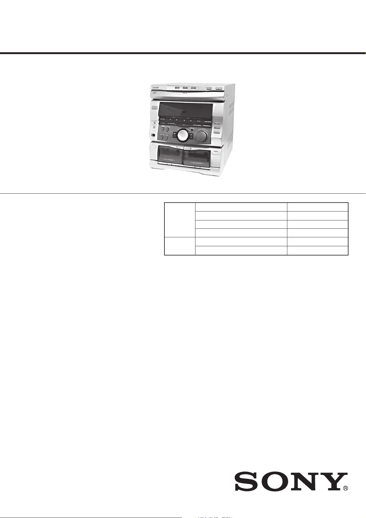
HCD-GRX3/RX55/R300 are the tuner, deck,
CD and amplifier section in MHC-GRX3/
RX55/R300.
photo : HCD-GRX3
Model Name Using Similar Mechanism HCD-G101
CD
SECTION
TAPE DECK
SECTION
CD Mechanism Type CX3
Base Unit Type KSM-213BCM
Optical Pick-up Type KSS-213B/S-N
Model Name Using Similar Mechanism NEW
Tape Transpor Mechanism Type
US Model
Canadian Model
HCD-RX55
E Model
HCD-GRX3/R300
Australian Model
HCD-GRX3
CWB44RR10
SPECIFICATIONS
AUDIO POWER SPECIFICATIONS:
(U.S.A. model only)
POWER OUTPUT AND TOTAL HARMONIC DISTORTION:
with 6 Ω loads both channels driven, from 70 – 20,000 Hz; rated 35 W per
channel minimum RMS power, with no more than 0.9% total harmonic
distortion from 250 mW to rated output.
Amplifier section
North American model
Continuous RMS power output
50 W + 50 W (6 Ω at 1 kHz, 10% THD)
Other models
The following measured at AC 110, 220 V 60 Hz;
DIN power output (Rated) 35 W + 35 W (6 Ω at 1 kHz, DIN)
Continuous RMS power output (Reference)
45 W + 45W (6 Ω at 1 kHz, 10% THD)
The following measured at AC 120, 240 V 60 Hz;
DIN power output (Rated) 40 W + 40 W (6 Ω at 1 kHz, DIN)
Continuous RMS power output (Reference)
50 W + 50W (6 Ω at 1 kHz, 10% THD)
Peak music power output (Reference)
600 W
Inputs
MD IN (phone jacks) : voltage 450 mV, impedance 47 kΩ
Outputs
MD OUT (phone jacks) : voltage 250 mV, impedance 1 kΩ
PHONES (stereo phone jack) :
accepts headphones of 8 Ω or more
SPEAKER : accepts impedance of 6 to 16 Ω
CD player section
System Compact disc and digital audio system
Laser Semiconductor laser (λ = 780 nm)
Emission duration: continuous
Laser output Max. 44.6 µW*
*This output is the value measured at a
distance of 200 mm from the objective
lens surface on the Optical Pick-up Block
with 7 mm aperture.
Frequency response 20 Hz – 20 kHz (± 0.5 dB)
Wavelength 780 – 790 nm
DIGIT AL OUT (OPTICAL)
(Square optical connector jack, rear panel)
Wavelength 600 nm
Output Level –18 dBm
Tape deck section
Recording system 4 -track 2 -channel stereo
Frequency response 40 – 13,000 Hz (± 3dB), using Sony
TYPE Ι cassette
— Continued on next page —
MINI Hi-Fi COMPONENT SYSTEM
9-922-804-12
2001K1600-1
© 2001.11
Sony Corporation
Home Audio Company
Published by Sony Engineering Corporation
Page 2
SERVICING NOTE
Antenna terminals 75 Ω unbalanced
Intermediate frequency 10.7MHz
AM tuner section
Tuning range 531 – 1,602 kHz (with AM tuning interval set
Antenna AM loop antenna
Antenna terminals External antenna terminal
Intermediate frequency 450 kHz
General
Power requirements
North American model:120 V AC, 60 Hz
Mexican model: 120 V AC, 50/60 Hz
Australian and South African models:
Other models: 110 – 120 V or 220 – 240 V AC,
Power consumption 100 W
Dimensions (w/h/d) incl. projecting parts and controls
Mass Approx. 9.5 kg (20 lb 15 oz.)
Supplied accessories: AM loop antenna (1)
Design and specifications are subject to change without notice.
at 9 kHz)
530 – 1,710 kHz (with AM tuning interval set
at 10 kHz)
220 – 240 V AC, 50/60 Hz
50/60 Hz (adjustable with voltage selector)
Approx. 280 × 320 × 400 mm
1
(11
/8 × 12 5/8 × 15 3/4 in)
Remote (1)
RM-SG7 (for HCD-GRX3/RX55)
RM-SG7B (for HCD-R300)
FM lead antenna (1)
NOTES ON HANDLING THE OPTICAL PICK-UP BLOCK
OR BASE UNIT
The laser diode in the optical pick-up block may suffer electrostatic
break-down because of the potential difference generated by the
charged electrostatic load, etc. on clothing and the human body.
During repair, pay attention to electrostatic break-down and also
use the procedure in the printed matter which is included in the
repair parts.
The flexible board is easily damaged and should be handled with
care.
NOTES ON LASER DIODE EMISSION CHECK
The laser beam on this model is concentrated so as to be focused on
the disc reflective surface by the objective lens in the optical pickup block. Therefore, when checking the laser diode emission,
observe from more than 30 cm away from the objective lens.
CAUTION
Use of controls or adjustments or performance of procedures
other than those specified herein may result in hazardous
radiation exposure.
Notes on chip component replacement
• Never reuse a disconnected chip component.
• Notice that the minus side of a tantalum capacitor may be
damaged by heat.
Flexible Circuit Board Repairing
• Keep the temperature of soldering iron around 270˚C
during repairing.
• Do not touch the soldering iron on the same conductor of the
circuit board (within 3 times).
• Be careful not to apply force on the conductor when soldering
or unsoldering.
SAFETY-RELATED COMPONENT WARNING!!
COMPONENTS IDENTIFIED BY MARK ! OR DOTTED LINE WITH
MARK ! ON THE SCHEMATIC DIAGRAMS AND IN THE PARTS
LIST ARE CRITICAL TO SAFE OPERATION. REPLACE THESE
COMPONENTS WITH SONY PARTS WHOSE PART NUMBERS
APPEAR AS SHOWN IN THIS MANUAL OR IN SUPPLEMENTS
PUBLISHED BY SONY.
Laser component in this product is capable of emitting radiation
exceeding the limit for Class 1.
This appliance is classified as
a CLASS 1 LASER product.
The CLASS 1 LASER
PRODUCT MARKING is
located on the rear exterior.
This caution
label is located
inside the unit.
ATTENTION AU COMPOSANT AYANT RAPPORT
À LA SÉCURITÉ!
LES COMPOSANTS IDENTIFÉS PAR UNE MARQUE ! SUR LES
DIAGRAMMES SCHÉMATIQUES ET LA LISTE DES PIÈCES SONT
CRITIQUES POUR LA SÉCURITÉ DE FONCTIONNEMENT. NE
REMPLACER CES COMPOSANTS QUE PAR DES PIÈSES SONY
DONT LES NUMÉROS SONT DONNÉS DANS CE MANUEL OU
DANS LES SUPPÉMENTS PUBLIÉS PAR SONY.
— 2 —
Page 3
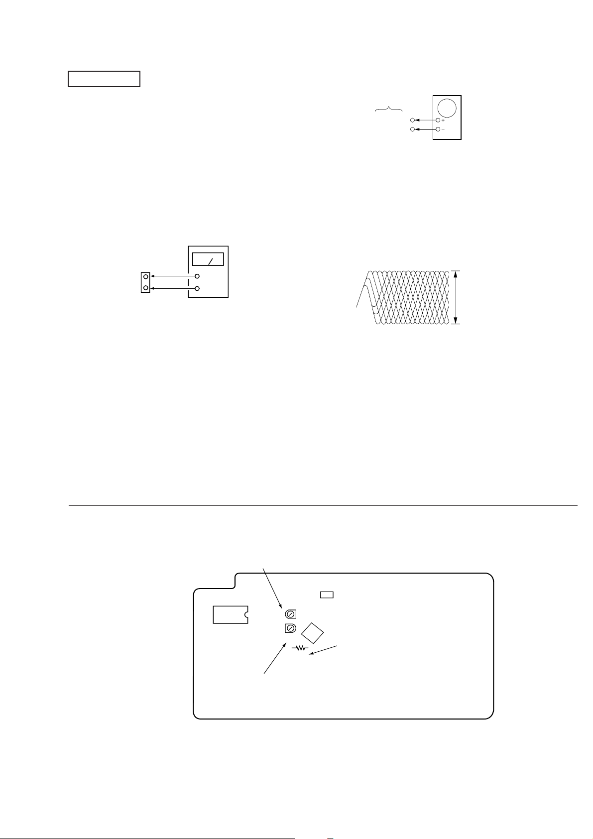
SAFETY CHECK-OUT
After correcting the original service problem, perform the following
safety checks before releasing the set to the customer:
Check the antenna terminals, metal trim, “metallized” knobs, screws,
and all other exposed metal parts for AC leakage. Check leakage as
described below.
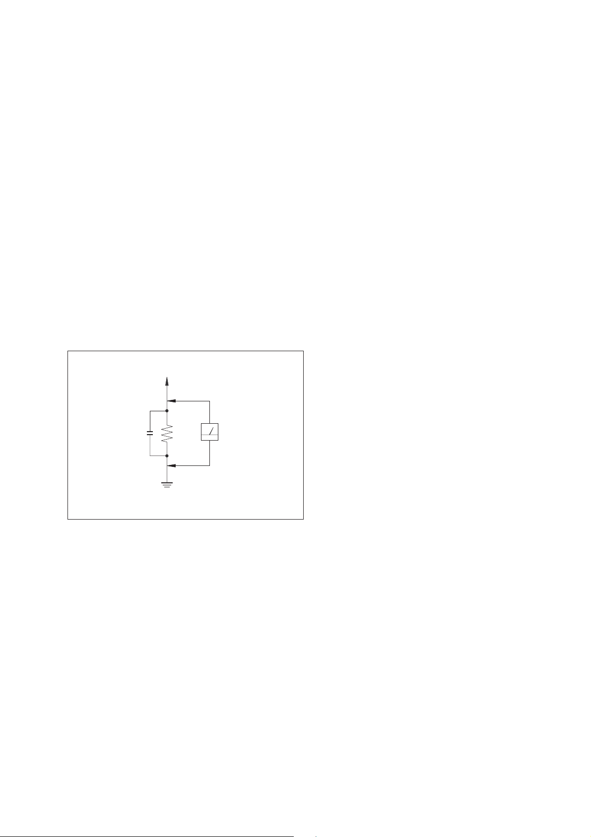
LEAKAGE
The AC leakage from any exposed metal part to earth Ground and
from all exposed metal parts to any exposed metal part having a
return to chassis, must not exceed 0.5 mA (500 microampers).
Leakage current can be measured by any one of three methods.
1. A commercial leakage tester , such as the Simpson 229 or RCA
WT -540A. Follow the manufacturers’ instructions to use these
instruments.
2. A battery-operated AC milliammeter. The Data Precision 245
digital multimeter is suitable for this job.
3. Measuring the voltage drop across a resistor by means of a
VOM or battery-operated AC voltmeter . The “limit” indication
is 0.75 V, so analog meters must have an accurate low-voltage
scale. The Simpson 250 and Sanwa SH-63Trd are examples of
a passive VOM that is suitable. Nearly all battery operated
digital multimeters that have a 2V AC range are suitable. (See
Fig. A)
T o Exposed Metal
Parts on Set
AC
0.15
µ
F
1.5 k
Ω
Voltmeter
(0.75 V)
TABLE OF CONTENTS
1. GENERAL ..........................................................................4
2. DISASSEMBLY
2-1. Upper Cover and CD Door................................................. 5
2-2. Front Panel .........................................................................5
2-3. Main Board ......................................................................... 6
2-4. Amp Board ......................................................................... 6
2-5. CD Tray .............................................................................. 7
2-6. CD Decoder Board ............................................................. 7
2-7. Base Unit ............................................................................ 8
2-8. Cassette Door .....................................................................8
3. MECHANICAL ADJUSTMENTS ............................... 9
4. ELECTRICAL ADJUSTMENTS .................................9
5. DIAGRAMS
5-1. Circuit Boards Location ................................................... 14
5-2. Block Diagrams
• Deck Section ................................................................... 15
• CD Section ...................................................................... 17
5-3. IC Block Diagrams ........................................................... 19
5-4. Printed Wiring Board —CD Section — ........................... 24
5-5. Schematic Diagram — CD Section — ............................. 29
5-6. Schematic Diagram —Panel Section — .......................... 33
5-7. Printed Wiring Board —Panel Section —........................ 37
5-8. Printed Wiring Board — Deck Section — ....................... 42
5-9. Schematic Diagram —Deck Section — ........................... 47
5-10. Schematic Diagram —Main Section — ........................... 51
5-11. Printed Wiring Board —Main Section — ........................ 55
5-12. Printed Wiring Board — Amp Section — ........................ 60
5-13. IC Pin Function ................................................................ 65
Earth Ground
Fig. A. Using an A C v oltmeter to check A C leakage.
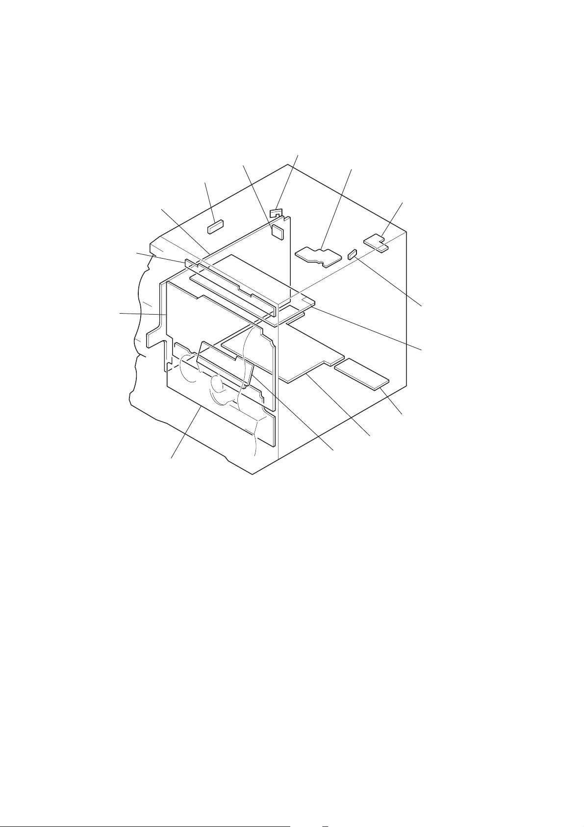
6. EXPLODED VIEWS
6-1. Cabinet Section................................................................. 67
6-2. Front Panel Section .......................................................... 68
6-3. Cassette Mechanism Deck Section................................... 69
6-4. CD Mechanism Deck Section 1 ....................................... 70
6-5. CD Mechanism Deck Section 2 ....................................... 71
6-6. Base Unit Section (KSM-213BCM)................................. 72
7. ELECTRICAL PARTS LIST ........................................ 73
— 3 —
Page 4
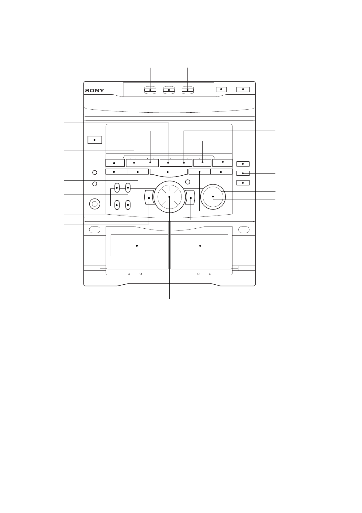
LOCATION OF PARTS AND CONTROLS
SECTION 1
GENERAL
#¡
#º
@ª
@•
@¶
@§
@∞
@¢
@£
@™
@¡
@º
1
23
4
5
6
7
8
9
0
!¡
!™
!£
!¢
!∞
!ª
1 DISC 1 button
2 DISC 2 button
3 DISC 3 button
4 DISC SKIP button
5 § OPEN/CLOSE button
6 · (TAPE B)
7 · ∏ (CD) button
8 TUNER/BAND button
9 r REC button
!º ∏ PAUSE button
!¡ CD SYNC button
!™ STEREO/MONO button
!£ VOLUME
!¢ REPEAT/MEMORY button
!∞ ‚ + button
!§ DECK B
!§
!¶!•
!¶ JOG DIAL
!• π (STOP) button
!ª DECK A
@º º – button
@¡ DBFB button
@™ SURROUND button
@£ FILE SELECT button
@¢ DISPLAY/DEMO button
@∞ EDIT/DIRECTION button
@§ PLAY MODE button
@¶ FUNCTION
@• ª (TAPE A) button
@ª I/u (POWER) button
#º · (TAPE A) button
#¡ ª (TAPE B) button
— 4 —
Page 5
SECTION 2
s
e
DISASSEMBLY
Note : Follow the disassembly procedure in the numerical order given.
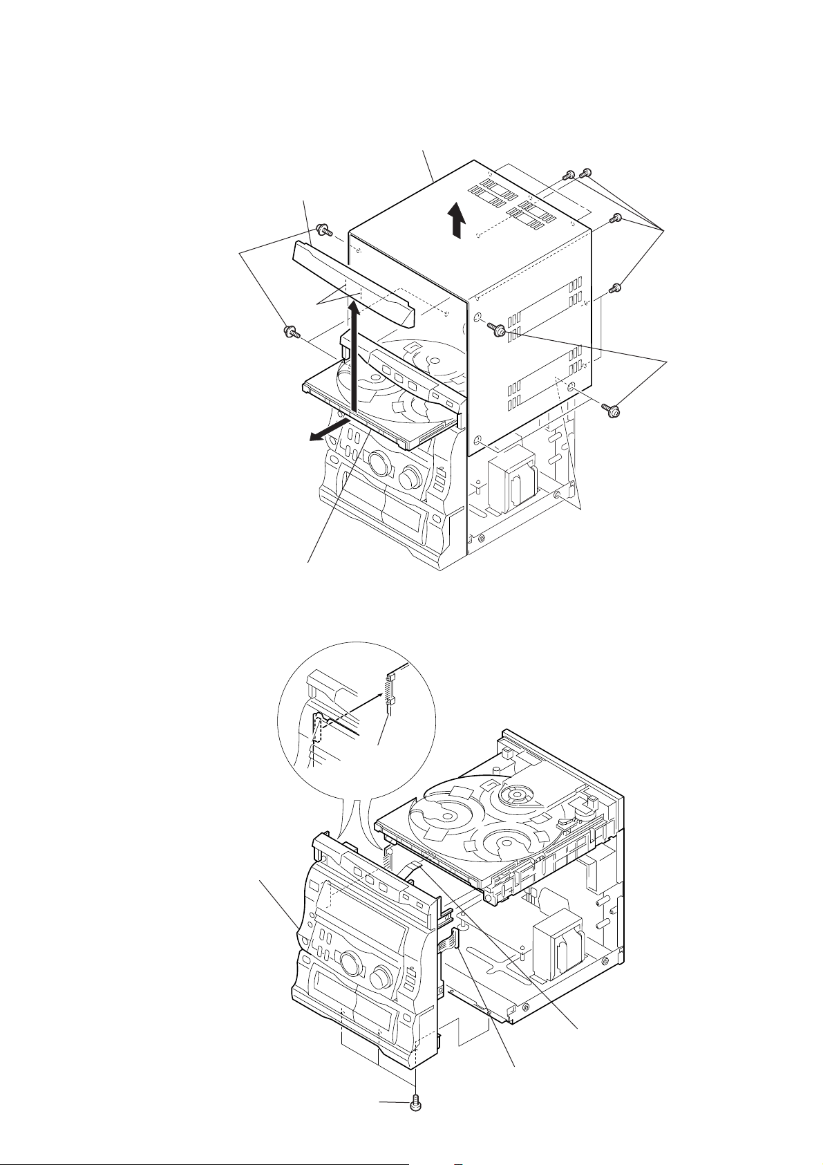
2-1. UPPER COVER AND CD DOOR
6
CD door
2
Three screws
claws
4
Upper cover
3
Seven screw
1
Three srews
2-2. FRONT PANEL
5
Pull out the CD tray and remove the
CD door with releasing craws into the
directioin of arrow.
4
Flat type wire
(CN09)
5
Front panel
1
Three screws
— 5 —
2
Connector
(CN302)
3
Flat type wir
(CN09)
Page 6
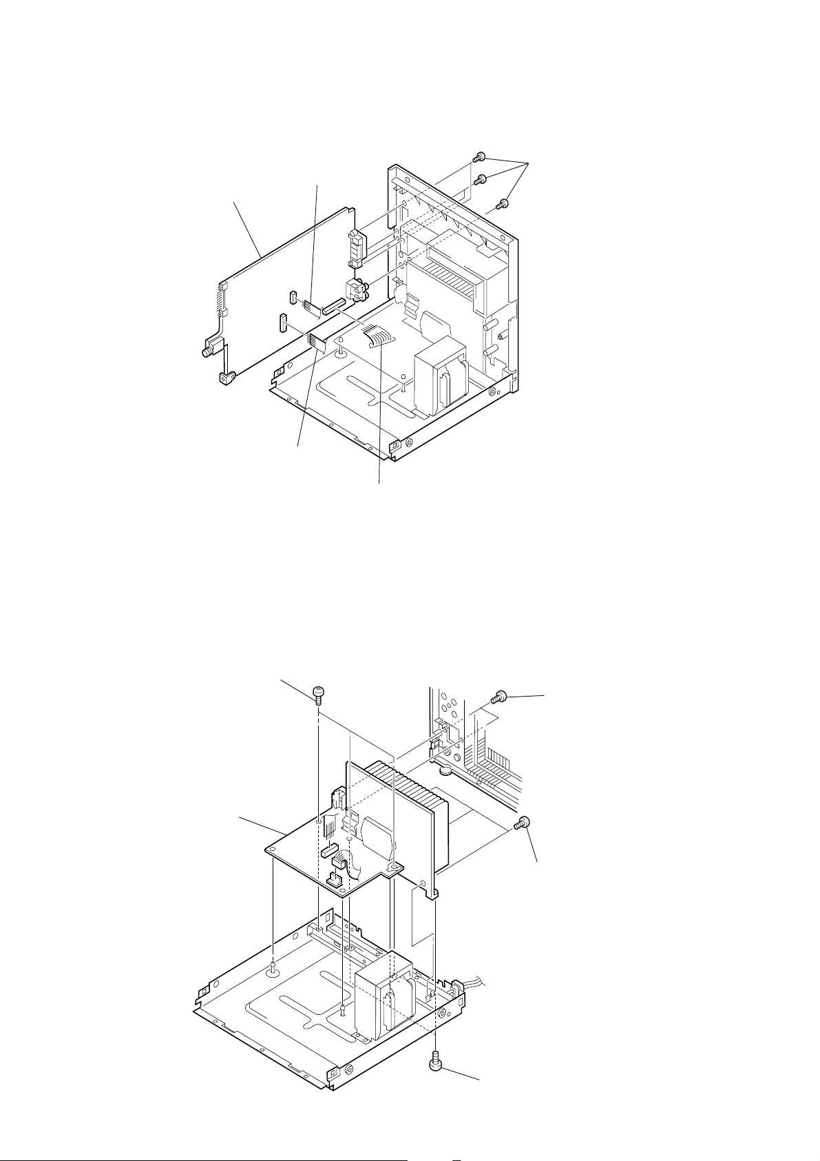
2-3. MAIN BOARD
5
MAIN board
4
Harness (CN08)
3
Harness (CN302)
2
Harness (CN701)
1
Five screws
2-4. AMP BOARD
5
AMP board
4
Three screws
1
Two screws
2
Three screws
— 6 —
3
Three screws
Page 7
e
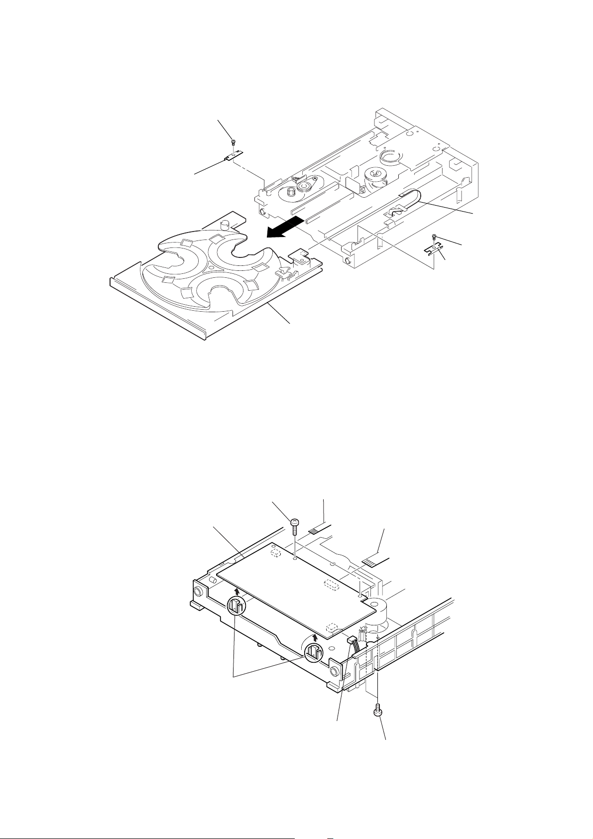
2-5. CD TRA Y
2
Bracket
1
Screw
6
CD tray
4
Bracket
5
(CN06)
3
Screw
Flat type wir
2-6. CD DECODER BOARD
6
CD decoder board
claws
2
Two screws
3
Flat cable
5
Connector
4
Flat cable
— 7 —
1
Two screws
Page 8
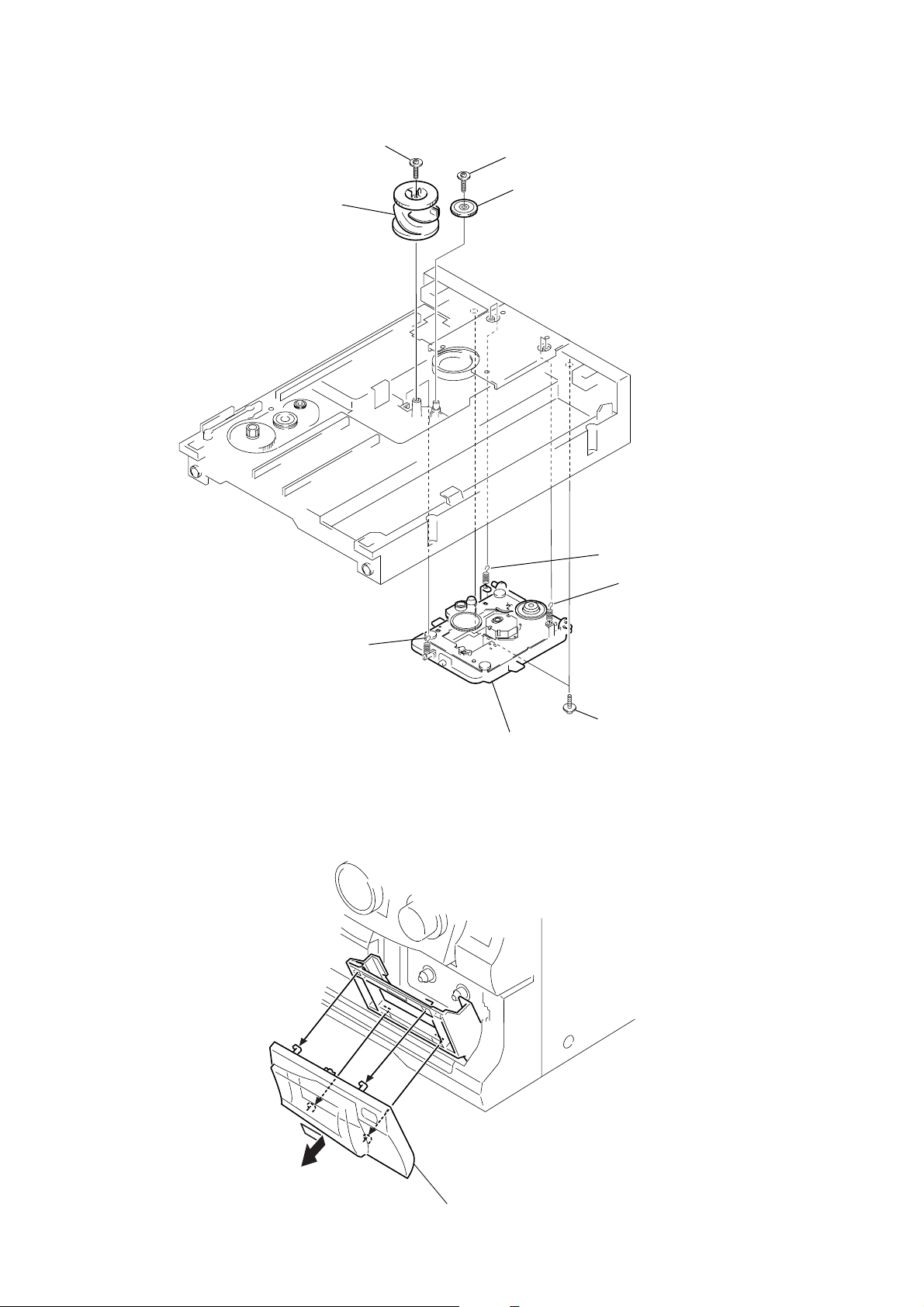
2-7. BASE UNIT
5
UD-Cam
4
Screw
2
3
Screw
UD-gear
7
Spring
2-8. CASSETTE DOOR
8
Spring
9
Base unit
6
Spring
1
Two screws
— 8 —
Cassette door
(Note: Four claws are used.)
Page 9
SECTION 3
MECHANICAL ADJUSTMENTS
SECTION 4
ELECTRICAL ADJUSTMENTS
Precaution
1. Clean the following parts with a denatured alcohol-moistened
swab:
record/playback head pinch rollers
erase head rubber belts
capstan idlers
2. Demagnetize the record/playback head with a head
demagnetizer.
3. Do not use a magnetized screwdriver for the adjustments.
4. After the adjustments, apply suitable locking compound to the
parts adjusted.
5. The adjustments should be performed with the rated power
supply voltage unless otherwise noted.
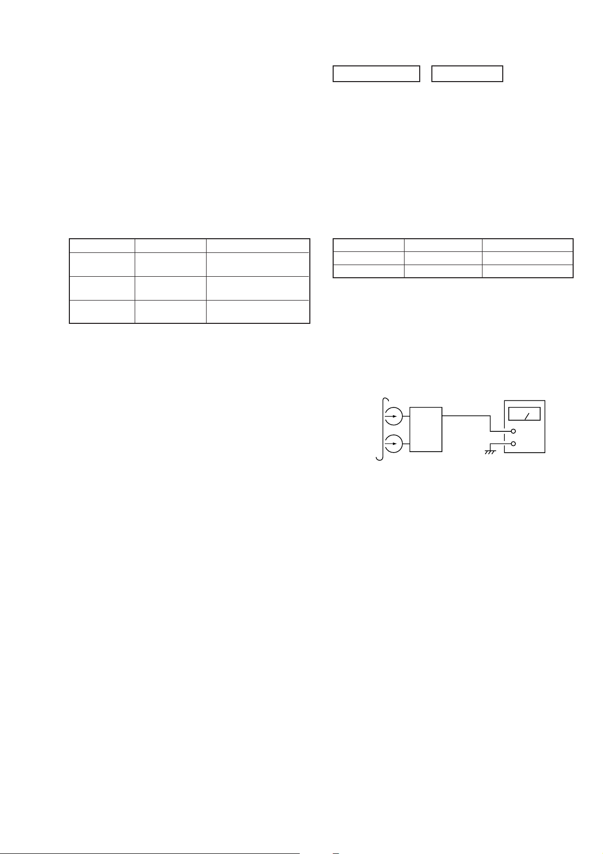
Torque Measurement
Torque
FWD
FWD
back tension
FF/REW
Torque meter
CQ-102C
CQ-102C
CQ-201B
Meter reading
40 to 70 g • cm
(0.56 - 0.97 oz • inch)
1 to 5 g • cm
(0.01 - 0.07 oz • inch)
55 to 140 g • cm
(0.76 - 1.94 oz • inch)
DECK SECTION 0 dB=0.775V
1. Demagnetize the record/playback head with a head
damagnetizer.
2. Do not use a magnetized screwdriver for the adjustments.
3. After the adjustments, apply suitable locking compound to the
parts adjusted.
4. The adjustments should be performed with the rated power
supply voltage unless otherwise noted.
5. The adjustments should be performed in the order given in this
service manual. (As a general rule, playback circuit adjustment
should be completed before performing recording circuit
adjustment.)
6. The adjustments should be performed for both L-CH and RCH.
Tape
P-4-A100
WS-48B
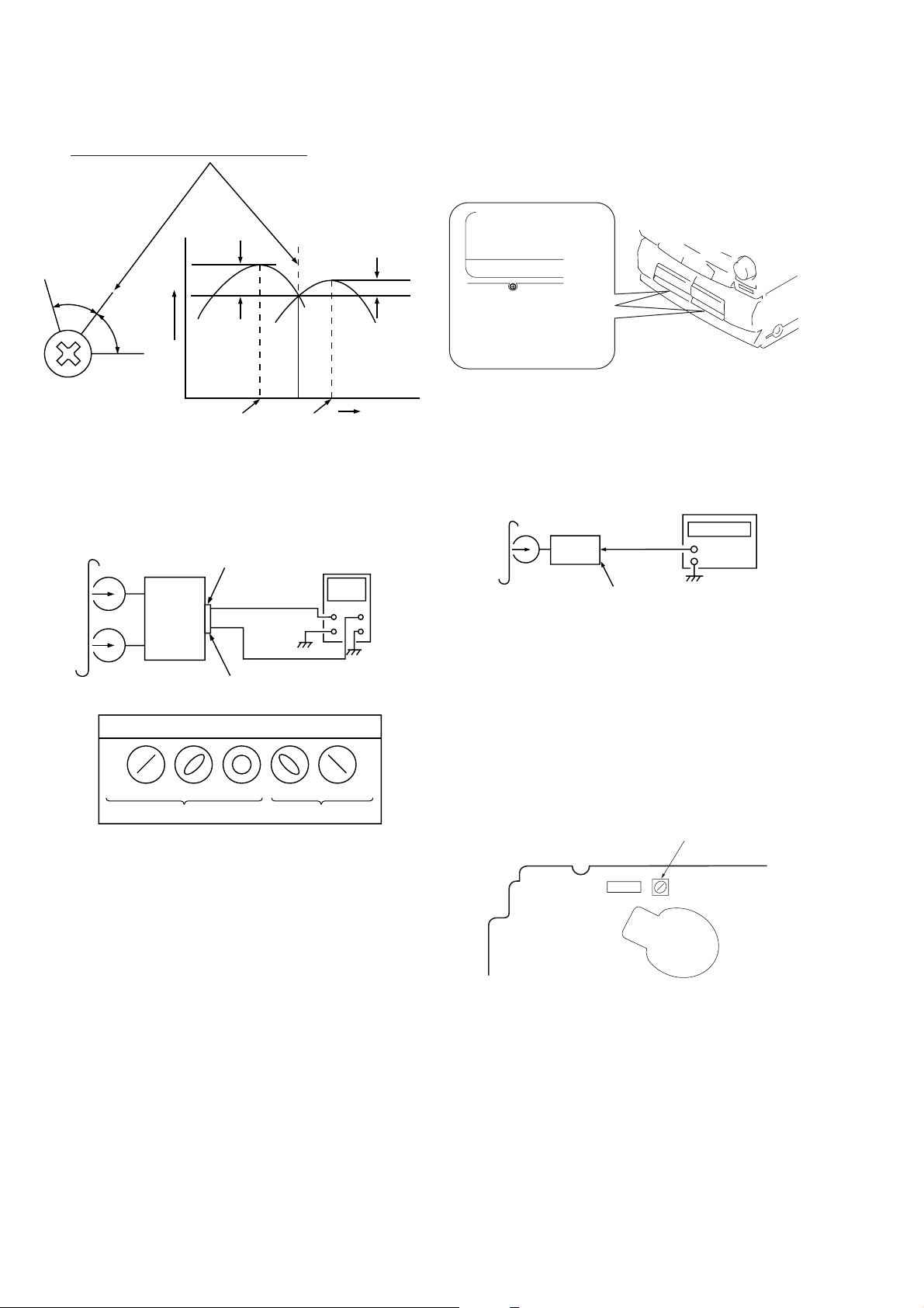
Record/Playback Head Azimuth Adjustment
(Deck A, Deck B)
Note: Perform this adjustments for both decks.
Procedure:
1. Mode : Playback
test tape
P-4-A100
(10kHz, –10dB)
Signal
10 kHz, –10 dB
3 kHz, 0 dB
SPEAKER
terminal (JK301)
Used for
Azimuth Adjustment
Tape Speed Adjustment
level meter
set
+
–
— 9 —
Page 10
2. Turn the adjustment screw and check output peaks. If the peaks
do not match for L-CH and R-CH, turn the adjustment screw
so that outputs match within 2 dB of peak.
L-CH
peak
screw
position
R-CH
peak
output
level
within
2dB
L-CH
peak
R-CH
peak
within 2dB
screw
position
3. Mode: Playback
test tape
P-4-A100
(10kHz, –10dB)
SPEAKER
terminal (JK301)
(L-CH)
oscilloscope
4. After the adjustments, apply suitable locking compound to the
parts adjusted.
Adjustment Location:
Adjustment screws
REC/PB head (deck A)
or PB head (deck B)
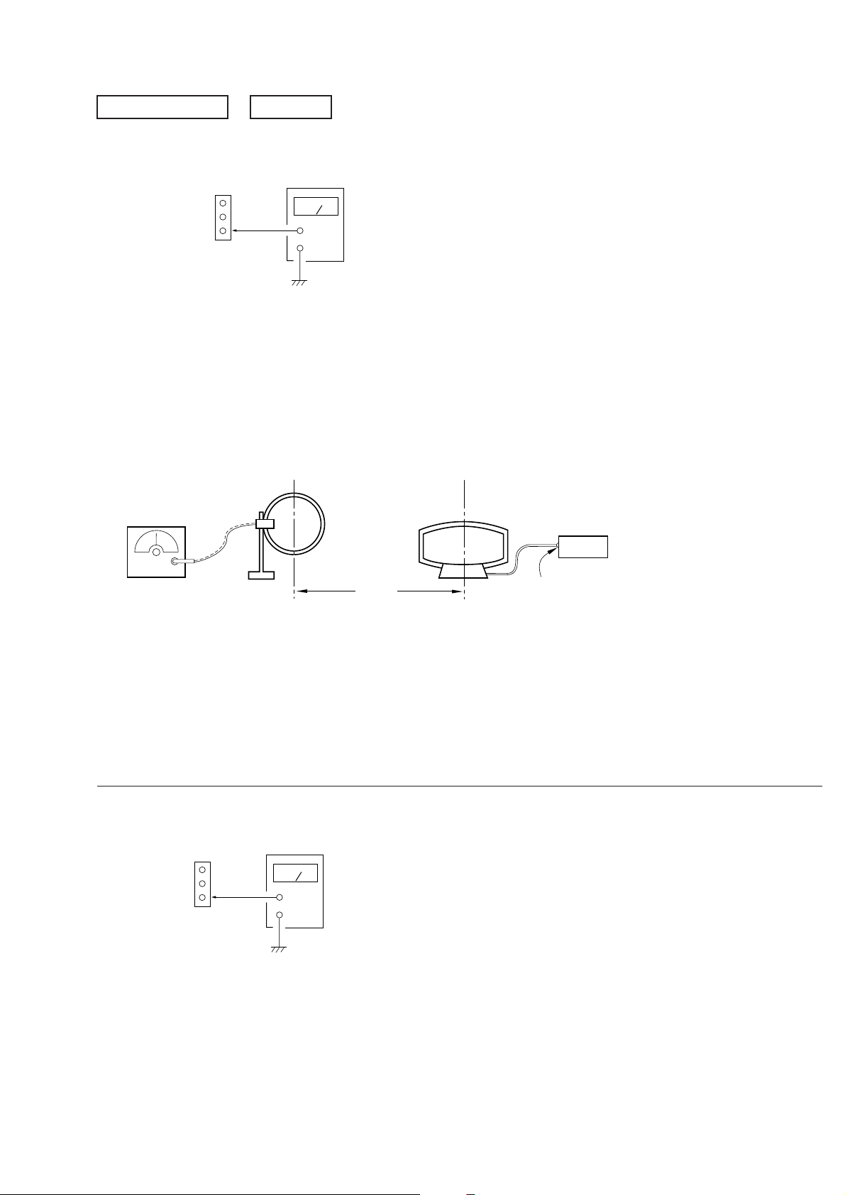
Tape Speed Adjustment (Deck A)
Procedure:
1. Mode: Playback
test tape
WS-48B
(3kHz, 0dB)
set
frequency counter
+
–
L
set
R
SPEAKER
terminal (JK301)
(R-CH)
Waveform of oscilloscope
in phase 45˚ 90˚ 135˚ 180˚
good
wrong
SPEAKER
terminal (JK301)
2. Adjust the SFR501 so that the frequency counter reads 3,000
Hz ± 90Hz.
Adjustment Location: DECK board
Sample Value of Wow and flutter
W. RMS (JIS) within 0.3%
(test tape: WS-48B)
[DECK BOARD] — Component side —
Tape Speed
CN501
SFR501
— 10 —
Page 11
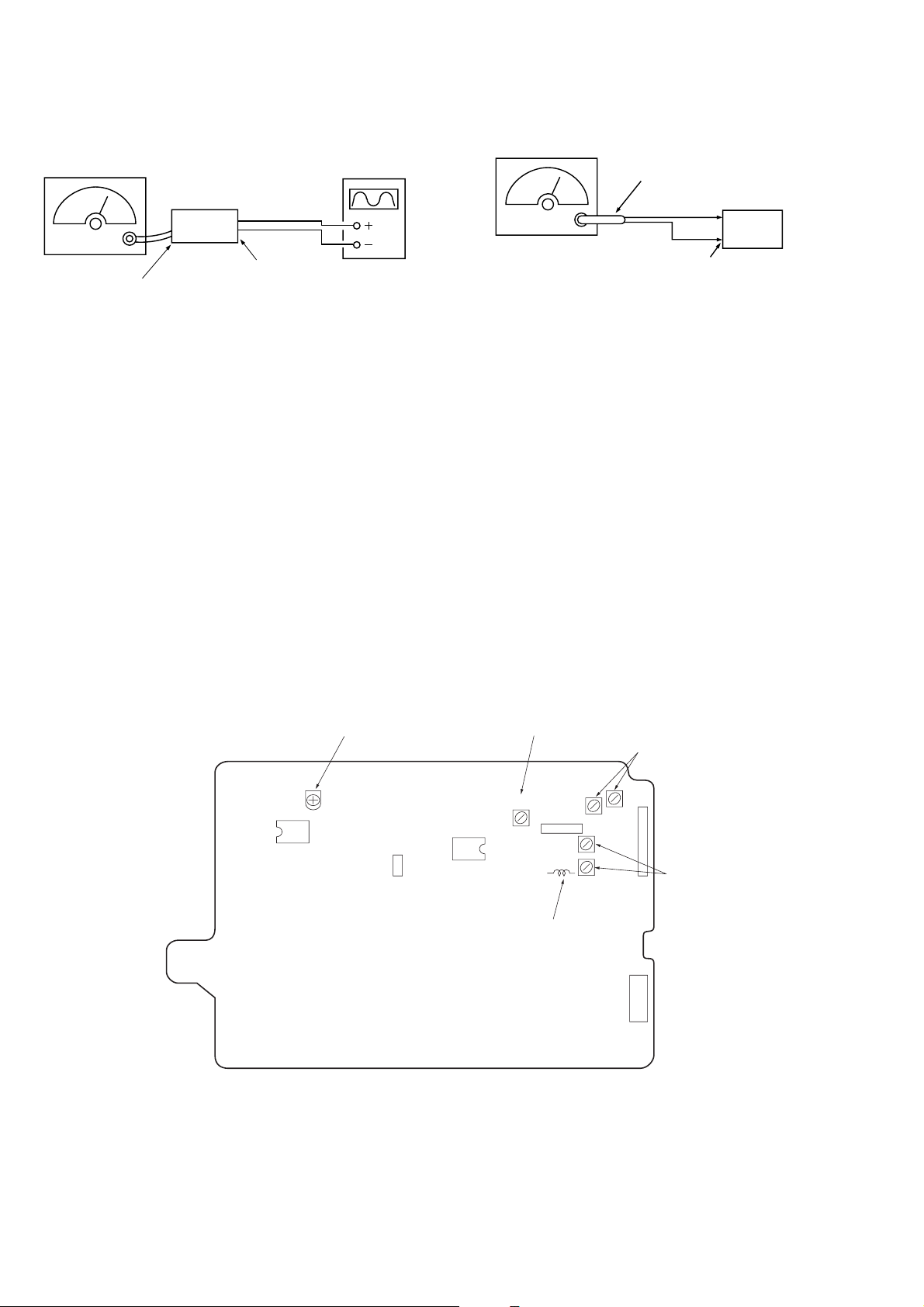
TUNER SECTION 0 dB=1µV
AM T uning Voltage Adjustment
Main board
TP1
F
G
VT
DC voltmeter
+
–
Procedure:
1. Set the reception frequency of the unit to 530 kHz.
2. Adjust L105 for 1.2 ± 0.05 V reading on the DC voltmeter.
3. Set the reception frequency of the unit to 1,710 kHz.
4. Confirm that the voltage reading on the DC voltmeter is within
8.0 ± 0.5 V.
Adjustment Location: MAIN board (See page 12)
AM Trac king Adjustment
loop antenna
AM RF SSG
30% amplitude
modulation by
400 Hz signal
60 cm
Field strength dB (
µ
V/m) =SSG output level dB (µV/m) –26 dB.
loop antenna
(Supplied accessories)
set
AM ANTENNA
terminal (JK101)
Procedure:
1. Tune the set to 600 kHz.
2. Set the output of AM RF SSG so that the input level of the set
will become 60 dB (µV/m).
3. Adjust L104 so that when the waveform on the oscilloscope is
maximum, no noise appears.
4. Tune the set to 1,400 kHz.
FM T uning Voltage Adjustment
Main board
TP1
IF
G
VT
DC voltmeter
+
–
Procedure :
1. Set the reception frequency of the unit to 87.5 MHz.
2. Adjust L103 for 1.2 ± 0.05V reading on the DC voltmeter.
3. Set the reception frequency of the unit to 108 MHz.
4. Confirm that the voltage reading on the DC voltmeter is within
7.8 ± 0.5V.
5. Adjust CT102 so that when the waveform on the oscilloscope
is maximum, no noise appears.
• Repeat the procedures in each adjustment several times, and the
tracking adjustment should be finally done by the trimmer
capacitors.
Adjustment Location: MAIN board (See page 12)
Adjustment Location: MAIN board (See page 12)
— 11 —
Page 12
FM Trac king Adjustment
FM Tuned Level Adjustment
Procedure:
FM RF SSG
set
SPEAKER terminal (JK301)
FM ANTENNA terminal (JK101)
Carrier frequency: 90 MHz, 106 MHz
Modulation : AUDIO 1kHz, 75kHz deviation (100%)
Output level : 20 dB (at 75
Ω
open)
oscilloscope
1. Tune the set to 90 MHz.
2. Adjust L102 so that when the waveform on the oscilloscope is
maximum, no noise appears.
3. Tune the set to 106 MHz.
4. Adjust CT101 so that when the waveform on the oscilloscope
is maximum, no noise appears.
• Repeat the procedures in each adjustment several times, and the
tracking adjustment should be finally done by the trimmer
capacitors.
Adjustment Location: MAIN board
FM RF SSG
75
Ω
coaxial
set
Carrier frequency : 98 MHz
Modulation : AUDIO 1 kHz, 75 kHz
Output level : 28 dB (at 75
deviation (100%)
Ω
open)
FM ANTENNA terminal
(JK101)
Procedure:
1. Supply a 28 dB 98 MHz signal from the ANTENNA terminal.
2. Tune the set to 98 MHz.
3. Adjust SFR101 to the point (moment) when the TUNED
indicator will change from going off to going on.
Adjustment Location: MAIN board
Adjustment Location
[MAIN BOARD] — Component side —
IC103
FM Tyned Level
SFR101
TP1
IC102
AM Tuning
Voltage
L105
FM Tuning
Voltage
CT102
IC101
L103
L102
CT101
AM
Tracking
L104
JK101
FM
Tracking
JK301
— 12 —
Page 13
CD SECTION
Note:
1. CD Block is basically constructed to operate without
adjustment. Therefore, check each item in order given.
2. Use YEDS-18 disc (3-702-101-01) unless otherwise indicated.
3. Use an oscilloscope with more than 10MΩ impedance.
4. Clean the object lens by an applicator with neutral detergent
when the signal level is low than specified value with the
following checks.
5. Adjust the focus bias adjustment when optical block is replaced.
Focus Bias Adjustment
CD DECODER
board
CN12
FEO
VC
Procedure:
1. Connect DC voltmeter to test point CN12 (FEO), (VC) on CD
DECODER board.
2. Turned Power switch on.
3. Put disc (YEDS-18) in and stop.
4. Adjust VR01 so that the DC voitmeter reading is 0 ± 20 mV.
DC voltmeter
+
–
RF Level Check
CD DECODER
board
TP (RF)
CN12 (VC)
oscilloscope
Procedure :
1. Connect oscilloscope to test point TP (RF) on CD DECODER
board.
2. Turned Power switch on.
3. Put disc (YEDS-18) in and playback.
4. Confirm that oscilloscope waveform is clear and check RF
signal level is correct or not.
Note: Clear RF signal waveform means that the shape “◊” can be
clearly distinguished at the center of the waveform.
VOLT/DIV: 200 mV
TIME/DIV: 500 nS
level: 1.0 Vp-p
+0.3
–0.2
Adjustment Location: CD DECODER board
Adjustment Location: CD DECODER board
Focus Gain Adjustment (VR02)
This gain has a margin, so even if it is slightly off.
There is no problem.
Therfore, do not perform this adjusment.
Please note that it should be fixed to mechanical center position
when you moved and do not know original position.
Adjustment Location
[CD DECODER BOARD] — Component side —
Focus Gain
VR02
IC03
VR01
R07
CN12
IC01
RF Level
Focus Bias
— 13 —
Page 14
5-1. CIRCUIT BOARDS LOCATION
d
SW (C) board
SECTION 5
DIAGRAMS
SW (D) board
SW (B) board
MOTOR (6P) (S) board
CD BUTTON board
PANEL board
MAIN board
DECK board
MOTOR board
SW (A) board
CD DECODER boar
FUSE board
AMP board
VOLUME board
— 14 —
Page 15
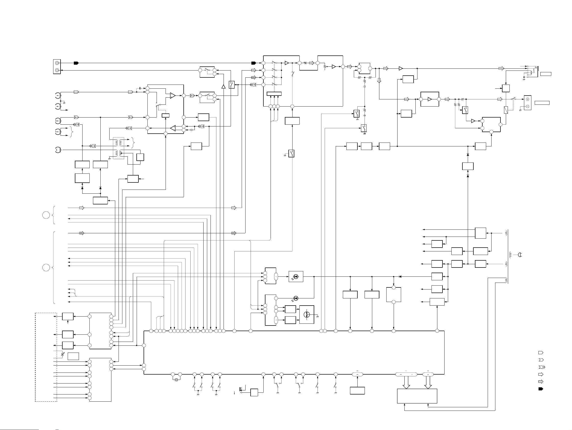
5-2. BLOCK DIAGRAMS
HCD-GRX3/RX55/R300
— DECK SECTION —
JK301
MD L
LINE
OUT L
TAPE B
HP901
PB
HEAD
R CHR CH
TAPE A
HRP901
REC/PB
HEAD
HE901
ERASE
HEAD
TU L
ST IND
A
TU MUTE
TUNER
SECTION
B
CD
SECTION
MECHA BLOCK
MTR +12V
SOL A
SOL B
SOL B
MOTOR H
MOTOR L
REC FWD
REC REV
PHOTO A
PHOTO B
MODE A
MODE B
HALF A
HALF B
16
CD L
SCOR
SENS
SQSO
XLAT
SQCK
DATA
COUNT
FOK
CLK
STB
DO
DI
CE
Q501,502
MOTOR
B+ SW
+12V
Q505,506
SOL A
DRIVE
Q503,504
SOL B
DRIVE
SFR 501
TAPE
SPEED
R CH
Q203,205
PLAY/REC
CONTROL
Q207
PLAY/REC
CONTROL
DRIVE
D202
Q208,209
BUS REGISTER
4
PLAY
5
SOL A
6
SOL B
SHIFT REGISTER
3
F REC
4
R REC
5
PHOTO A
6
PHOTO B
11
A MODE
12
B MODE
13
A HALF
14
B HALF
Q201
PLAY/REC
CONTROL
CONTROL
SWITCH
IC501
REC MUTE
IC502
D201
REC
BIAS
STB
CLK
SELECTOR
IC301
DI
CLK
36
ALATCH
Q605,615
SW
11
9
10
12
CONTROL
CLK14DI15CE
13
CLKDICE
LED DRIVE
IC603
1
12
3
17
2
LED DRIVE
IC602
13
2
11
3
12
4
10
5
SYSTEM CONTROLLER/
FLD DRIVER
PIC UP55PIC DOWN56TRAY OPEN
MODE
13
S01
CD DECK
UP/DOWN
DET
IC601
IC302 (1/2)
11 10
IC302 (2/2)
9 8
Q551,552
AMS
MUTE
24
4
DI1
SCOR
TU MUTE
VR DOWN
45
A
B
12
6
47
61
FM ST IND
JOG A49JOG B
VR612
MULTI JOG
Q417
AMS
50
62
6
TAPE REC
B
Q301
SERI MUTE
SW101
10k
5
SURROUND
+5.6V
9k
REC/PB
EQ AMP
IC201
3
1
2
9
BIAS
OSC
Q251
Q251
43
42
41
+12V
26
DECK STB
DECK DATA
DECK S/L
TAPE A/B
STB
L251
BIAS OSC
R CH
Q252,253
BIAS
SWITCH
14
12
A/B
11
13
S/I
Q'S
QH
S/L
DO
2
CLK
3
10
1
2
9
1
CE
21CE22
CLK
CLK
A/B
REC OUT
19
DO
23DO52
PB OUT
MIX OUT
FOK
12
12
4.19MHz
53
COUNT
X601
5
6
11
10
Q213
REC
MUTE
18
19
51
20
SQCK
38
XLAT
SENS
SQSO
VR UP
44
A
VR601
VOLUME
17
DATA
X211X1
LT COM
4
Q307
SURROUND
CONTROL
Q310
LED606-611
LED605
Q606,607
LED
DRIVE
Q608-613
LED
DRIVE
OPEN/CLOSE
3 2
LED601-604
TRAY CLOSE
59
60
S02
TRAY
DET
DISC COUNT
57
S03
DISC
COUNTER
DET
7
8
DBFB HIGH
DBFB NORMAL
3
SYSTEM MUTE
TURN TABLE
58
S04
TURNTABLE
OPERATION
DET
1
Q602
Q602
NORMAL
Q603
MUTE
SWITCH
RESET
SWITCH
10
Q331
HIGH
Q308
RESET
KI0 KI4
KEY
MATRIX
S601-628
LINE AMP
IC303
4
3
Q604
MUTE
Q601
Q601
2
POWER
DOWN DET
15
POWER DOWN
Q410
MUTE
DRIVE
RM601
CONTROL
RECEIVER
3
REMOTE
2
39
HP AMP
IC401
3
D602
REMOTE
64 78
1
Q408
MUTE
Q709
MUTE
+30V
-30V
-12V
-27V
+7.5V
+11.5V FILTER
+11.5V
(SWITCHED)
P1 P21
.
81 8533 29
FLD601
FLD DISPLAY
POWER AMP
IC401
1
G1 G15
100 86
10
Q401
-12V
REG
Q702
+7.5V
REG
Q409
+5.6V
REG
Q403
Q415,416
SITCHING
2
POWER
Q703
-27V
REG
Q701
+12V
REG
Q713
P MUTE
CONT
Q706
D718
D720
Q708
1
2
Q714
AC OFF
DET
D701
RECT
D731,732
VOLTAGE
DOUBLER
D705-708
RECT
+12V
IC402
SPEAKER
RELAY
DRIVE
4
Q404
AC3.4V
AC3.4V
R CH
SP
DET
RL701
6
PT001
AC
IN
JK303
PHONES
JK302
SPEAKER
• RCH is omitted
• Signal Path
: PB (DECK A)
: PB (DECK B)
: REC (DECK A)
: FM
: CD
: MD
— 15 — — 16 —
Page 16
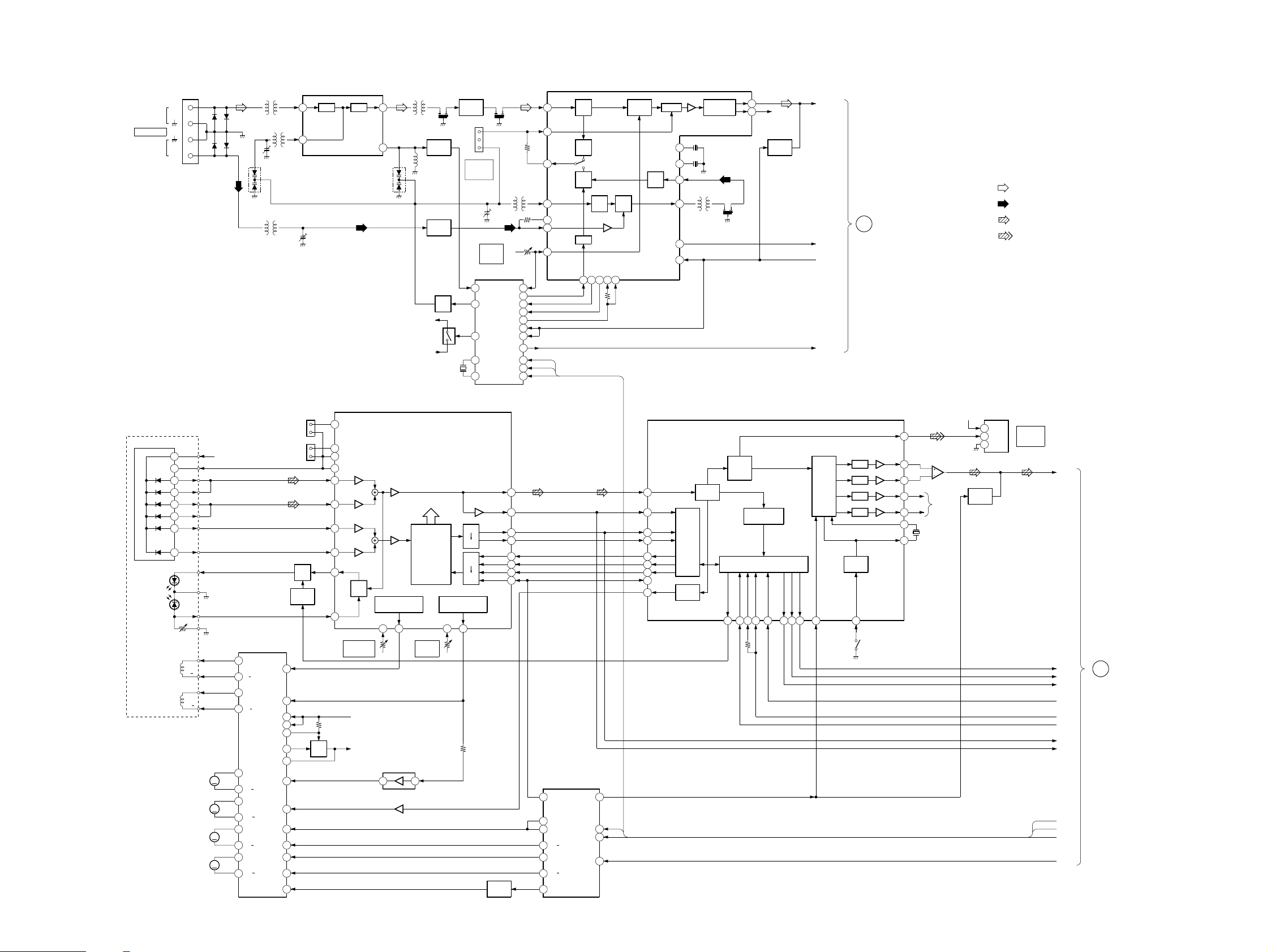
HCD-GRX3/RX55/R300
— TUNER/CD SECTION —
JK101
ANTENNA
75Ω
AM
DET
DET
AGC
FM
IF
FM
AM
SMET
20
FM/AM MPX
IC102
AM
OSCAMMIX
PL DET
PH DET11PH DET
TU LED
13
6
L
CF103
450kHz
14
R
15
R CH
Q117
MUTE
AM/FM
IF BUFF
12
MUTE
FM DET
MPX VCO
AM
IF
ST IND
AM/FM
DECODER
CF104
8
10.7MHz
CF105
17
19kHz
4
T102
AM IFT
2
7
10
TU L
ST IND
TU MUTE
DI
A
MAIN
SECTION
• R CH is omitted
• SIGNAL PATH
:FM
:AM
:CD
:DIGITAL OUT
1
3
FM FRONT END
IC101
RF MIX
OSC
D106
CF101
10.7MHz
Q102
AMP
Q108
AM RF
AMP
Q112,113
L.P.F
7.2MHz
X101
Q101
RF IF
AMP
IF
G
VT
TP1
AM/FM
TUNING
VOLTAGE
19
21
17
24
1
SFR101
FM
TUNED
LEVEL
FM
PD1
FM B+
XO
XI
CF102
10.7MHz
PLL
IC103
ST/MONO
MW OSC
B+
AM/FM
L CTR
R CTR
CLK
FM IF
1
MPX
16
AF DET
18
L105
OSC
23
AFC
22
AM RF
21
OSC/FMSD
24
AM
18
12
SD
SD
7
14
13
15
16
DI
5
DO
DO
3
DI
CLK
4
CE
2
CE
T101
6
8
FM OSC
L103
TUB+
Q114
B+
L101
FM
FM ANT
D105
L104
AM ANT
L102
FM RF
OPTICAL PICK-UP
DETECTOR
TRACKING
16
BLOCK
LD
PD
FOCUS
COIL
COIL
7
8
4
1
2
5
6
10
GND
VR
MOTOR
SPINDOL
MOTOR
MOTOR
MOTOR
VC
A
C
B
D
E
F
LD
PD
F+
F
T+
T
M102
SLED
M101
T/T
TRAY
+5V
M
M
M
M
F/T COIL
SL/SP MOTOR
T.T/TRAY MOTOR
DRIVER
IC03
4
F+
3
F
2
T+
1
T
REG OUT
18
SL+
17
SL
SP+
20
SP
19
T.T F IN
14
T.T+
T.T R IN
T.T
15
TR F IN
TR+
30
TR T IN
TR
31
MUTE IN
F IN
T IN
VCC
VCC
REG I
REG B
SL IN
SP IN
6
5
8
7
9
10
11
22
21
13
12
29
28
27
Q02
LD ON
SWITCH
Q01
APC
CN2
CN12
Q11
REG
42
1
45
48
35
36
39
38
33
34
TEO
FEO
ATSC
VC
PD1
PD2
E
F
LD
APC
PD
PD
FE BIAS EI
RV01
FOCUS
TRACKING
+7.5V
+5V
RF
AMP
COMAND
FE
AMP
SERIAL/
PARALLEL
CONVERTER
DECODER
FOCUS PHASE
COMPENSATION
FEO TAO
6
37 40
16
IC01 (2/2)
IC06
RV02
FOCUS
GAIN
14
67
CD RF/SERVO
PROSSESOR
IC01 (1/2)
IIL
TTL
TTL
IIL
TRACKING PHASE
COMPENSATION
13
RFO
FOK
C OUT
SENS
DATA
XLT
CLK
XRST
Q04
SWITCH
+5V
PH01
2
Q311
MUTE
VDD
D IN
GND
OPTICAL
DIGITAL
OUT
CD L
SCOR
SENS
SQSO
XLAT
SQCK
DATA
COUNT
FOK
DO
CLK
CE
STB
B
MAIN
SECTION
(Page)
3
1
CD DIGITAL
SIGNAL PROCESSOR
IC703
D/A
I/F
RF
DO
CLK
36
FOK
23
CN
14
SE
13
DAT
15
XLT
16
CLK
17
8
XRST
MDP
25
31
25
23
24
21
20
19
22
T.T/TRAY
MOTOR DRIVE
REG CONTROL
IC02
XRST
SPEED
T.T
TR+
TR
CONTRL
MUTE
DATA
CLOK
STB
4
2
3
1
6
11
714T.T+
13
14
5
CLV
SERVO
DIGITAL
CLV
EFM
DEMO.
SUB CODE
PROSSESOR
CPU I/F
XLON
CLOCK
DATA
SQCK
9 11 5 4 7 61
22
XLAT
10
SQSO
SENS
SCOR
SERIAL
I/F
MUTE
S05
LIMIT
SWITCH
PWM
PWM
PWM
PWM
CLOCK
GEN.
SPOA
18
D OUT
XTA1
XTA0
61
NL
NR
MIX AMP
IC05
70
2
1
3
L
69
77
R
R-CH
78
73
X701
74
— 17 — — 18 —
Page 17
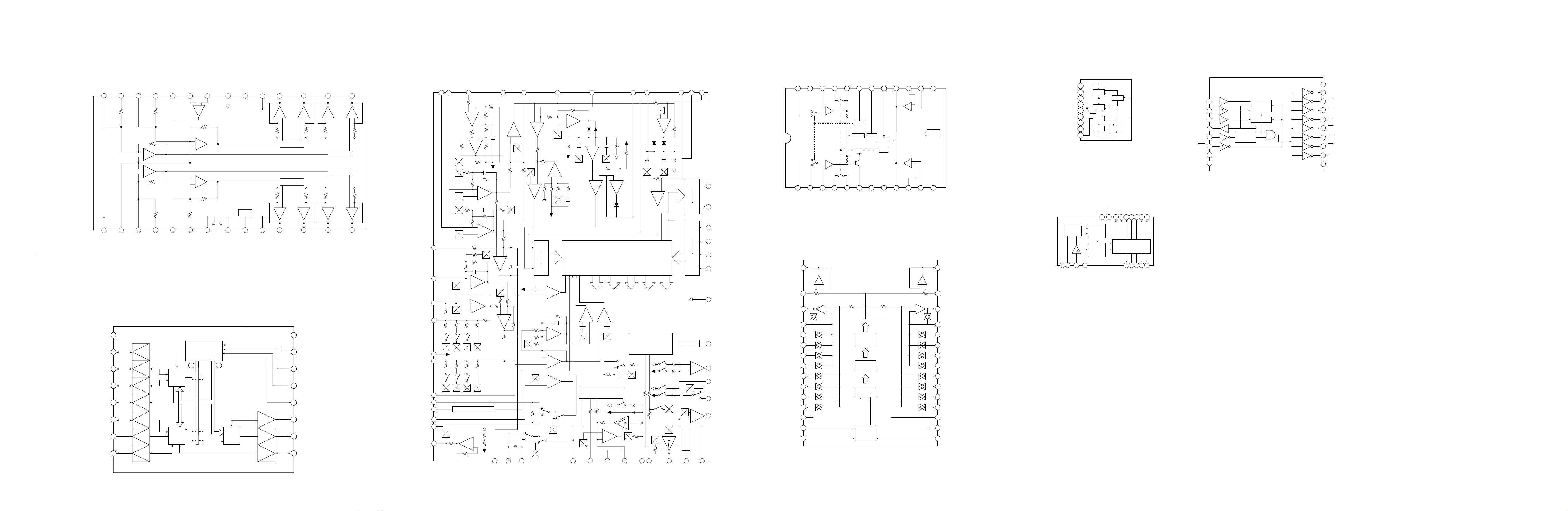
5-3. IC BLOCK DIAGRAMS
+
–
3
6
9
12
15
2
5
8
11
14
1
4
7
10
13
28
25
22
19
16
29
26
23
20
17
30
27
24
21
18
+
–
+–+
–
LATCH
DECODER
CONTROL
SHIFT
REGISTER
–
+
LVROUT
LVRIN
LTOUT
LTCOM
LT4
LT3
LT2
LT1
L4
L3
L2
L1
VDD
CL
DI
RVROUT
RVRIN
RTOUT
RTCOM
RT4
RT3
RT2
RT1
R4
R3
R2
R1
VREF
VSS
CE
CH2/A CH2/B NF VCC CG NF ALC
METAL
OUT
PRE
OUT
TAPE A
/TAPE B
REC
OUT
REC
IN
CH1/A CH1/B NF GND1 M/H NF
CH2
CH2
ALC
M/N
CH1
GNDGND
CH1
+
–
+
–
+
–
+
–
A/B
GNDMETAL
OUT
PRE
OUT
MIX
OUT
REC
OUT
REC
IN
IREF
VREF2
VREF1
24 23 22 21 20 19 18 17
16
15 14 13
123456789101112
HCD-GRX3/RX
IC03 (CD DECORD BOARD) BA5941FP
IN4B
IN4A
27
28
1 2
VCC
BIAS IN
IC02 (CD DECORD BOARD) TC9173P
CONTROL
T.T(M)
POSI.1
POSI.2
T.T.SW
GND
MUTE
XRST
1
2
3
4
5
6
7
8
IN3B
26
3
IN1B
DRIVER
IC01 (CD DECORD BOARD) CXA1782BQ IC101 (MAIN BOARD) LA1186
PHD2
37FE BIAS
38F
39E
40EI
41VEE
42TEO
43LPFI
44TEI
45ATSC
46TZC
47TDFCT
48VC
PHD1
36
35 34
IN3A
OP OUT
OP IN (–)
OP IN (+)
24
25
–
+
+
–
4
5
IN1A
IN2B
LATCH
23
6
IN2A
C
22
+
–
–
+
+
–
7
SERIAL I/O
CONTROL
GND
GND
NC
VCC
T
21 20
MUTE
8
GND
LATCHLATCH
NC
9
MUTE
19
Vcc
VccVcc
10
VCC
DRIVER
OUT3A
18
–
+
LEVEL SHIFT
LEVEL SHIFT
+
–
11
OUT2A
+
+
12 13
16
VDD
15
STB
14
CLOK
DATA I
13
12
DATA 0
11
LOADING
M-
10
LOADING
M+
SENSOR
9
OUT3B
–
–
OUT2B
OUT4A
1617
–
+
LEVEL SHIFT
LEVEL SHIFT
+
–
OUT1A
+
+
OUT4B
15
–
–
14
OUT1B
— 19 — — 20 — — 21 — — 22 — — 23 —
F IV AMP
BAL1
BAL2
TOG1
TOG2
• WINDOW COMP
PHD
–
+
–
+
APC
+
RF IV AMP1
RF IV AMP2
–
+
–
+
E IV AMP
BAL3
TOG3
ATSC
–
+
LD
33
–
–
+
+
–
FE AMP
+
–
TE AMP
1
FEO
RF M
32
–
+
–
+
LEVELS
+
–
FOK
TTL
IIL
FZC COMP
DFCT
3
2
FEI
FDFCT
DFCT
FS4
31
–
–
+
–
+
–
+
+
–
TZC COMP
RF O
–
+
RF I
30
–
+
+
+
–
MIRR
• IIL DATA RESISTOR • INPUT SHIFT RESISTOR
TOG1-3 FS1-4 TG1-2 TM1-7 PS1-4
BAL1-3
–
+
HPF COMP LPF COMP
• FCS PHASE
COMPENSATION
TM1
5
4
FLB
FGD
–
+
FS2
+
–
6
FE O
+
–
• ADDRESS DECODER
• OUTPUT DECODER
TG1
FS1
7
FE M
CB
29CP28
DFCT
• TRACKING
• PHASE
COMPENSATION
9
8
SRCH
TGU
–
TM7
TG2
+
TM6
TM5
TM4
TM3
CC126CC225FOK
27
–
+
24 SENS
IIL
TTL
23 C. OUT
22 XRST
TTL
21 DATA
20 XLT
IIL
19 CLK
18 VCC
• ISET
• F SET
11
10
TG2
FSET
TM2
17 ISET
–
16 SL 0
+
15 SL M
14 SL P
+
1312TA O
–
TA M
IC201 (MAIN BOARD) TA8189N
IC301 (MAIN BOARD) LC75392
1
RF IN
2
3
4
5
6
7
8
9
RF
VREF
MIX
REG
OSC BUF
BYPAS
MIX IN
GND
GND
IF
AFC
OSC
VCC
IC602 (PANEL BOARD) BU2092
CONTROL
CIRCUIT
2 3
1
VSS
DATA
CLOCK
4
LCK
12 BIT
SHIFT
REGISTER
12 BIT
STORAGE
REGISTER
VDDOEQ11
1718
Q10Q9Q8Q7Q6
OUTPUT
BUFFER
(OPEN DRAIN)
5 6 7 8 9
Q0
IC603 (PANEL BOARD) BU2114
18
VDD
17
O1
SIN
1
CK
2
3
LATCH
SOUT
4
5
EN
RST
6
GND
7
8
GND
Q5
1016 15 14 13 12 11
Q4
Q3
Q2
Q1
ENABLE
SHIFT
REGISTER
LATCH
16
O2
15
O3
14
O4
13
O5
12
O6
O7
11
10
O8
9
GND
Page 18

Page 19

Page 20

Page 21

Page 22

Page 23

Page 24

Page 25

Page 26

Page 27

5-13. IC PIN FUNCTION
IC601 µPD780205FG (SYSTEM CONTROL) / PANEL BOARD
Pin No.
1
2
3
4
5
6
7
8
9
10
11
12
13
14
15
16
17
18
19
20
21
22
23
24
25
26
27
28
29
30
31
32
33
34
35
36
37
38
39
40
41
42
43
44
45
46
47
48
49
50
Pin Name
VDD
POWER OUT
S. MUTE OUT
TU. MUTE OUT
TUNED OUT
TAPE REC OUT
DBFB NORMAL
NC
NC
RESET
X2
X1
VSS
NC
POWER DOWN IN
VDD
SOCK
DATA
SOSO
XLAT
CE
CLK
DO
DI
VSS
CD STB
FLAT
VSS
K4
K3
K2
K1
K0
AVDD
AVREF
A LATCH
B LATCH
SCOR
REMOTE IN
VSS
NC
VSS
DECK STB
VR UP
VR DOWN
VDD
FM ST IN
SYNC REC IN
VSS
VSS
I/O
—
VDD
O
Power switch output. ON: H, OFF: L
O
System mute output. ON: H, OFF: L
O
Tuner mute output. ON: H, OFF: L
O
Surround output. ON: H, OFF: L (Not used)
O
Function tape output. Tape: H, Others: L (Not used)
O
DBFB normal (U2: DBFB). ON: H, Others: L
O
DBFB high. ON: H, Others: L (Not used)
—
Not used
—
Reset input
I
X’tal 4.194314 MHz
I
X’tal 4.194314 MHz
—
Ground
—
Not used (open)
I
Power down input. AC ON: H, AC OFF: L
—
VDD
O
CXD2508A SQCK, CLOCK output
O
CXD2508A data output
I
CXD2508A SQSO input
O
CXD2508A XLAT output. Latch: L, Others: H
O
Chip enable output to LC7218, LC75392. Data: H, Address: L
O
CLK output
O
Data output
I
Data input
—
Ground
O
STB output to SN74HC4094. STB: L, Others: H
O
Flat output. Flat: H, Others: L (Not used)
—
Ground
I
Key input 4 to A/D
I
Key input 3 to A/D
I
Key input 2 to A/D
I
Key input 1 to A/D
I
Key input 0 to A/D
O
VDD of A/D converter
—
Reference voltage of A/D converter
O
Latch output to BU2092. Latch: H, Others: L
—
Not used
I
CXD2508A SCOR
I
Remote signal input. ON: H, OFF: L
—
Ground
O
Shift or load output to SN74HC165. Shift: H, Load: L (Not used)
I
Data input to SN74HC165 (Ground)
O
STB output to BU2114, SN74HC4094. STB:H, Others: L (Not used)
I
VR encoder A input. ON:L, OFF: H
I
VR encoder B input. ON:L, OFF: H
—
VDD
I
FM stereo indicator input. Stereo:L, Mono: H
I
Synchro record input. Record:L, Other: H
I
CD encoder A input. ON: L, OFF: H (Ground)
I
CD encoder B input. ON: L, OFF: H (Ground)
Description
— 65 —
Page 28

Pin No.
51
52
53
54
55
56
57
58
59
60
61
62
63
64
65
66
67
68
69
70
71
72
73
74
75
76
77
78
79
80
81
82
83
84
85
86
87
88
89
90
91
92
93
94
95
96
97
98
99
100
Pin Name
SENS
FOK
COUNT
VSS
PIC UP
PIC DOWN
DISC COUNT SW
TURN T ABLE SW
TRAY OPEN SW
TRAY CLOSE SW
VSS
SERI MUTE
(TUNER)
MODE SW IN
P1
P2
P3
P4
P5
P6
P7
P8
P9
P10
P11
P12
P13
P14
P15
–V LOAD
P16
P17
P18
P19
P20
P21
G15
G14
G13
G12
G11
G10
G9
G8
G7
G6
G5
G4
G3
G2
G1
I/O
I
Input from CXD2508A SENS
I
Input from CXD2508A FOK. OK: H, Others: L
I
Input from CXD2508A COUNT
—
Ground
I
Input from CD mechanism pick up switch. Up: L, Others: H
I
Input from CD mechanism pick down switch. Down: L, Others: H
I
Input from CD mechanism disc count switch. Count: L, Others: H
I
Input from CD mechanism turn table switch. ON: L, OFF: H
I
Input from CD mechanism tray open switch. Open: L, Others: H
I
Input from CD mechanism tray close switch. Open: L, Others: H
I
AMS signal input. During program: H, Interval between programs: L
O
Serial mute (tuner) output (Not used)
I
Input from destination select mode switch. ON: H, OFF: L
O
FLD segment signal output P1. ON: H, OFF: L
O
FLD segment signal output P2. ON: H, OFF: L
O
FLD segment signal output P3. ON: H, OFF: L
O
FLD segment signal output P4. ON: H, OFF: L
O
FLD segment signal output P5. ON: H, OFF: L
O
FLD segment signal output P6. ON: H, OFF: L
O
FLD segment signal output P7. ON: H, OFF: L
O
FLD segment signal output P8. ON: H, OFF: L
O
FLD segment signal output P9. ON: H, OFF: L
O
FLD segment signal output P10. ON: H, OFF: L
O
FLD segment signal output P11. ON: H, OFF: L
O
FLD segment signal output P12. ON: H, OFF: L
O
FLD segment signal output P13. ON: H, OFF: L
O
FLD segment signal output P14. ON: H, OFF: L
O
FLD segment signal output P15. ON: H, OFF: L
—
(–) negative power supply
O
FLD segment signal output P16. ON: H, OFF: L
O
FLD segment signal output P17. ON: H, OFF: L
O
FLD segment signal output P18. ON: H, OFF: L
O
FLD segment signal output P19. ON: H, OFF: L
O
FLD segment signal output P20. ON: H, OFF: L
O
FLD segment signal output P21. ON: H, OFF: L
O
FLD grid signal output 15. ON: H, OFF: L
O
FLD grid signal output 14. ON: H, OFF: L
O
FLD grid signal output 13. ON: H, OFF: L
O
FLD grid signal output 12. ON: H, OFF: L
O
FLD grid signal output 11. ON: H, OFF: L
O
FLD grid signal output 10. ON: H, OFF: L
O
FLD grid signal output 9. ON: H, OFF: L
O
FLD grid signal output 8. ON: H, OFF: L
O
FLD grid signal output 7. ON: H, OFF: L
O
FLD grid signal output 6. ON: H, OFF: L
O
FLD grid signal output 5. ON: H, OFF: L
O
FLD grid signal output 4. ON: H, OFF: L
O
FLD grid signal output 3. ON: H, OFF: L
O
FLD grid signal output 2. ON: H, OFF: L
O
FLD grid signal output 1. ON: H, OFF: L
Description
— 66 —
Page 29

SECTION 6
EXPLODED VIEWS
NOTE:
• -XX, -X mean standardized parts, so they may
have some differences from the original one.
• Items marked “*” are not stocked since they
are seldom required for routine service. Some
delay should be anticipated when ordering these
items.
• Abbreviation
CND : Canadian
AUS : Australian
MX : Mexico
AED : North European
SP : Singapore
MY : Malaysia
6-1. CABINET SECTION
2
#10
#10
• The mechanical parts with no reference number
in the exploded views are not supplied.
• Hardware (# mark) list and accessories and
packing materials are given in the last of this
parts list.
TW : Taiwan
AR : Argentine
G : German
#10
#11
#10
3
#11
4
#3
When indicating parts by reference number,
please include the board name.
The components identified by mark ! or
dotted line with mark ! are critical for safety .
Replace only with part number specified.
Les composants identifiés par une marque
! sont critiques pour la sécurité.
Ne les remplacer que par une pièce portant
le numéro spécifié.
5
#11
#11
#3
#11
#12
12
#11
#10
#4
1
#14
PT302
CD mechanism deck
#14
#4
#14
7
8
#3
13
#2
#3
#11
6
10
9
#11
Ref. No. Part No. Description Remarks Ref. No. Part No. Description Remarks
1 4-210-584-01 WINDOW, CD
* 2 4-210-616-01 COVER (-GRX), TOP
3 4-210-579-01 HOLDER, MAIN PC BOARD
* 4 A-4405-480-A MAIN BOARD, COMPLETE (US,CND)
* 4 A-4405-482-A MAIN BOARD, COMPLETE (E,AUS,SP,MY,TW)
! 9 1-551-506-99 CORD, POWER (E,MX)
! 9 1-559-583-11 CORD, POWER (US,CND)
! 9 1-696-966-11 CORD, POWER (AUS)
! 9 1-765-558-11 CORD, POWER (SP,MY,TW)
* 10 3-703-244-00 BUSHING (2104), CORD (AUS,SP,MY,TW)
#11
not supplied
#3
#11
* 4 A-4405-483-A MAIN BOARD, COMPLETE (MX)
* 5 4-210-591-01 CABINET (A), REAR
* 6 4-210-617-01 COVER, REAR (US,CND)
* 6 4-210-618-01 COVER, REAR (E,SP,MY,TW)
* 6 4-210-619-01 COVER, REAR (AUS,MX)
* 7 A-4405-477-A AMP BOARD, COMPLETE (US,CND)
* 8 1-670-445-11 FUSE BOARD
10 3-703-571-11 BUSHING (S) (4516), CORD (US,CND,E,MX)
12 4-210-580-01 SPACER (SCC-20), PC BOARD
* 13 1-771-477-11 VOLSEL BOARD
! PT302 1-431-950-11 TRANSFORMER, POWER (US,CND)
! PT302 1-431-952-11 TRANSFORMER, POWER (E,AUS,SP,MY,TW)
! PT302 1-431-953-11 TRANSFORMER, POWER (MX)
— 67 —
Page 30

Ver 1.1 2001.11
6
6-2. FRONT PANEL SECTION
not supplied
86
73
not supplied
75
#16
83
#16
#16
56
55
60
58
57
61
51
62
79
52
81
64
65
53
#15
not
supplied
67
#15
63
54
59
80
#1
#16
#16
72
#16
#16
a
70
79
66
71
69
78
74
#16
77
#16
#16
84
76
#16
68
#15
81
#15
#16
#16
#16
a
63
#16
85
82
Cassette mechanism deck
Ref. No. Part No. Description Remarks Ref. No. Part No. Description Remarks
51 4-210-586-01 WINDOW (R), CASSETTE
52 4-210-588-01 DOOR (R), CASSETTE
53 4-210-577-01 SPRING (R), CASSETTE
54 4-210-572-01 HOLDER (R), CASSETTE
55 4-210-585-01 WINDOW (L), CASSETTE
56 4-210-587-01 DOOR (L), CASSETTE
57 4-210-576-01 SPRING (L), CASSETTE
58 4-210-571-01 HOLDER (L), CASSETTE
59 4-992-154-01 RUBBER, FOOT
60 4-210-592-01 WINDOW, DISPLAY
61 4-210-581-01 HOLDER, CD BUTTON
62 4-962-708-01 EMBLEM (4-A), SONY
63 4-992-131-01 DAMPER (GRY), GEAR
64 4-210-553-01 BUTTON, POWER
65 4-210-554-01 BUTTON, CLOCK
66 4-210-570-01 BUTTON (B), CD
67 4-210-556-01 BUTTON, MODE
68 4-210-560-01 BUTTON, REC
69 4-210-562-01 KNOB, VOLUME
70 4-210-561-01 KNOB, JOG
71 4-210-563-01 RING, JOG
72 4-210-593-01 PLATE, DISPLAY
73 4-210-558-01 BUTTON, SURROUND
74 4-210-557-01 BUTTON, NEXT
75 4-210-555-01 BUTTON, FUNCTION
76 4-210-559-01 BUTTON, UP/DOWN
77 4-210-552-01 PANEL (B), FRONT
78 4-210-574-01 WASHER (9Q), VOLUME
79 4-210-578-01 SPRING, EJECT LEVER
80 4-210-575-01 LEVER, EJECT
81 4-210-573-01 HOLDER, EJECT
82 4-210-551-01 PANEL (A), FRONT
* 83 A-4405-479-A PANEL BOARD, COMPLETE (US,CND,MX)
* 83 A-4405-485-A PANEL BOARD, COMPLETE (E,AUS,SP,MY,TW)
* 84 1-670-441-11 VOLUME BOARD
* 85 A-4414-609-A DECK BOARD, COMPLETE
* 86 1-670-443-11 CD BUTTON BOARD
— 68 —
Page 31

6-3. CASSETTE MECHANISM DECK SECTION
161
158
not supplied
157
160
159
151
164
not supplied
not supplied
160
154
154
156
162
153
155
not supplied
156
152
153
155
159
160
158
157
not supplied
not supplied
163
not supplied
not supplied
Ref. No. Part No. Description Remarks Ref. No. Part No. Description Remarks
151 1-759-633-11 DECK, MECHANICAL
152 9-880-883-01 HOLDER HEAD ASSY
153 9-880-884-01 FRAME HEAD
154 9-880-885-01 SPRING AZIMUTH
155 9-880-886-01 ARM PINCH L ASSY
156 9-880-887-01 ARM PINCH R ASSY
157 9-880-889-01 COIL ASSY
158 9-880-890-01 PLUNGER
159 9-880-891-01 MODE SW
160 9-880-892-01 SWITCH LEAF
161 9-880-893-01 BELT
162 9-880-894-01 HOLDER HEAD ASSY
163 9-880-895-01 BELT
164 9-880-896-01 MOTOR ASSY
— 69 —
Page 32

6-4. CD MECHANISM DECK SECTION 1
202
226
209
225
204
203
#5
223
211
218
216
217
222
#9
221
215
219
214
224
208
212
201
M103
205
206
212
213
#5
210
#7
#7
207
220
#5
225
Ref. No. Part No. Description Remarks Ref. No. Part No. Description Remarks
* 201 1-670-801-11 MOTOR BOARD
202 3-669-480-11 + PTPWH 2
203 4-992-168-01 TRAY, CHANGER BASE
204 4-992-180-01 PLATE, BLIND
205 4-992-181-01 LEVER, SENSOR (SW)
206 4-992-182-01 SPRING, SENSOR (SW) LEVER
207 4-992-170-01 BELT, LOADING
208 4-992-171-01 PULLEY, GEAR
209 4-992-179-01 GEAR, TR
210 4-992-177-01 GEAR, TR LOCK
211 4-992-178-01 GEAR (C), RELAY
212 4-992-187-01 CUSHION
213 4-992-186-01 CUSHION, SW LEVER
214 4-992-173-01 GEAR (B), RELAY
215 4-992-183-01 SCREW, RELAY GEAR (B)
216 4-992-174-01 GEAR, CHANGE
217 4-992-184-01 WASHER, CHANGE GEAR
218 4-992-176-01 SPRING, CHANGE GEAR
219 4-992-185-01 WASHER, CHANGE PLATE
220 4-992-172-01 GEAR (A), RELAY
* 221 4-993-032-01 PLATE, CHANGE
222 4-993-033-01 WASHER, POLY ETHYLENE
* 223 1-670-798-11 SW (B) BOARD
* 224 1-670-797-11 SW (A) BOARD
* 225 4-993-034-01 GUIDE, RAIL
226 4-993-140-01 TURN TABLE
M103 X-4948-765-1 MOTOR ASSY (TURN TABLE)
— 70 —
Page 33

6-5. CD MECHANISM DECK SECTION 2
not supplied
259
264
#1
255
M104
256
258
259
263
257
267
#7
#1
262
261
254
266
#1
#7
#1
252
#7
253
251
#10
268
Base unit block
#1
Ref. No. Part No. Description Remarks Ref. No. Part No. Description Remarks
251 1-769-856-11 WIRE (FLAT TYPE) (5 CORE)
252 4-992-190-01 UD-CAM
253 4-992-191-01 UD-GEAR
254 4-992-195-01 MAGNET
* 255 4-992-196-01 CHASSIS, MAIN
256 4-992-197-01 BELT, LOADING GEAR
257 4-992-198-01 PULLEY (B), GEAR
258 4-992-199-01 GEAR, SLIDE
259 4-992-200-01 ROLLER
261 4-992-192-01 SPRING, BRAKE CAM
262 4-992-193-01 LEVER, SW
* 263 1-670-800-11 SW (D) BOARD
* 264 1-670-799-11 SW (C) BOARD
266 4-992-194-01 CLAMP
267 4-992-201-01 WASHER, POLYETHYLENE
* 268 A-4414-924-A CD DECODER BOARD, COMPLETE
M104 X-4948-766-1 MOTOR ASSY (A) (TRAY)
— 71 —
Page 34

6-6. BASE UNIT SECTION (KSM-213BCM)
not supplied
307
302
#18
M102
#6
#6
M101
302
#6
303
306
308
310
305
#6
303
309
304
304
301
Ref. No. Part No. Description Remarks Ref. No. Part No. Description Remarks
301 4-992-164-01 BASE, KSM MECHANICAL
302 4-992-165-01 DAMPER (GREEN)
303 4-992-166-01 DAMPER (RED)
304 4-992-167-01 SPRING, MECHANICAL BASE
305 2-626-907-01 GEAR (A) (S)
306 2-626-908-01 SHAFT, SLED
307 2-627-003-02 GEAR (B)
! 308 8-848-379-31 OPTICAL PICK-UP KSS-213B/S-N
* 309 1-639-678-12 MOTOR (6P)(S) BOARD
310 1-783-740-11 WIRE (FLAT TYPE) (16 CORE)
M101 X-2625-877-1 MOTOR ASSY (SPINDLE)
M102 X-2625-769-1 MOTOR ASSY (SLED)
— 72 —
The components identified by
mark ! or dotted line with mark
! are critical for safety.
Replace only with part number
specified.
Les composants identifiés par
une marque ! sont critiques
pour la sécurité.
Ne les remplacer que par une
pièce portant le numéro spécifié.
Page 35

SECTION 7
ELECTRICAL PARTS LIST
AMP
NOTE:
When indicating parts by reference number,
please include the board name.
The components identified by mark ! or
dotted line with mark ! are critical for safety .
Replace only with part number specified.
Les composants identifiés par une marque
! sont critiques pour la sécurité.
Ne les remplacer que par une pièce portant
le numéro spécifié.
• Abbreviation
CND : Canadian
AUS : Australian
MX : Mexico
Ref. No. Part No. Description Remarks Ref. No. Part No. Description Remarks
* A-4405-477-A AMP BOARD, COMPLETE
* 1-533-293-11 FUSE HOLDER
C705 1-126-961-11 ELECT 2.2uF 20% 50V
C706 1-126-961-11 ELECT 2.2uF 20% 50V
C707 1-162-302-11 CERAMIC 0.0022uF 20% 16V
C709 1-126-967-11 ELECT 47uF 20% 16V
C710 1-126-967-11 ELECT 47uF 20% 16V
C711 1-126-968-11 ELECT 100uF 20% 50V
C712 1-126-967-11 ELECT 47uF 20% 16V
C715 1-126-967-11 ELECT 47uF 20% 16V
C716 1-126-964-11 ELECT 10uF 20% 50V
C719 1-137-150-11 FILM 0.01uF 5% 100V
TW : Taiwan
AR : Argentine
SP : Singapore
MY : Malaysia
*********************
< CAPACITOR >
• Due to standardization, replacements in the
parts list may be different from the parts
specified in the diagrams or the components
used on the set.
• -XX, -X mean standardized parts, so they may
have some difference from the original one.
• Items marked “*” are not stocked since they
are seldom required for routine service. Some
delay should be anticipated when ordering these
items.
• CAPACITORS:
uF: µF
C763 1-161-055-00 CERAMIC 0.022uF 10% 50V
C768 1-161-055-00 CERAMIC 0.022uF 10% 50V
C770 1-126-967-11 ELECT 47uF 20% 50V
C775 1-107-712-11 ELECT 3.3uF 20% 50V
C776 1-161-055-00 CERAMIC 0.022uF 10% 50V
C777 1-161-055-00 CERAMIC 0.022uF 10% 50V
C778 1-126-960-11 ELECT 1uF 20% 50V
C781 1-126-933-11 ELECT 100uF 20% 16V
C782 1-126-949-11 ELECT 220uF 20% 35V
C783 1-161-055-00 CERAMIC 0.022uF 10% 50V
C784 1-161-055-00 CERAMIC 0.022uF 10% 50V
C785 1-161-055-00 CERAMIC 0.022uF 10% 50V
CN703 1-564-510-11 PLUG, CONNECTOR 7P
• RESISTORS
All resistors are in ohms.
METAL: metal-film resistor
METAL OXIDE: Metal Oxide-film resistor
F: nonflammable
• COILS
uH: µH
• SEMICONDUCTORS
In each case, u: µ, for example:
uA...: µA... , uPA... , µPA... ,
uPB... , µPB... , uPC... , µPC... ,
uPD..., µPD...
< CONNECTOR >
C720 1-137-150-11 FILM 0.01uF 5% 100V
C721 1-137-354-11 FILM 0.1uF 5% 100V
C722 1-137-354-11 FILM 0.1uF 5% 100V
C723 1-126-961-11 ELECT 2.2uF 20% 50V
C724 1-137-150-11 FILM 0.01uF 5% 100V
C725 1-126-235-11 ELECT 100uF 20% 16V
C726 1-126-967-11 ELECT 47uF 20% 16V
C730 1-126-963-11 ELECT 4.7uF 20% 50V
C735 1-162-282-31 CERAMIC 100PF 10% 50V
C736 1-162-282-31 CERAMIC 100PF 10% 50V
C741 1-117-750-11 ELECT 3300uF 20% 63V
C742 1-117-750-11 ELECT 3300uF 20% 63V
C743 1-137-354-11 FILM 0.1uF 5% 100V
C744 1-137-354-11 FILM 0.1uF 5% 100V
C745 1-137-354-11 FILM 0.1uF 5% 100V
C746 1-137-354-11 FILM 0.1uF 5% 100V
C748 1-161-055-00 CERAMIC 0.022uF 10% 50V
C749 1-161-055-00 CERAMIC 0.022uF 10% 50V
C750 1-126-943-11 ELECT 2200uF 20% 25V
C752 1-126-933-11 ELECT 100uF 20% 16V
C753 1-161-055-00 CERAMIC 0.022uF 10% 50V
C754 1-161-055-00 CERAMIC 0.022uF 10% 50V
C755 1-126-948-11 ELECT 100uF 20% 35V
C756 1-126-948-11 ELECT 100uF 20% 35V
C757 1-161-055-00 CERAMIC 0.022uF 10% 50V
C758 1-126-949-11 ELECT 220uF 20% 35V
C759 1-161-055-00 CERAMIC 0.022uF 10% 50V
C760 1-126-933-11 ELECT 100uF 20% 16V
C761 1-161-055-00 CERAMIC 0.022uF 10% 50V
C762 1-126-935-11 ELECT 470uF 20% 16V
< DIODE >
D701 8-719-025-88 DIODE GBU4JL-6088
D705 8-719-031-85 DIODE 1N4002L
D706 8-719-031-85 DIODE 1N4002L
D707 8-719-031-85 DIODE 1N4002L
D708 8-719-031-85 DIODE 1N4002L
D711 8-719-110-31 DIODE RD12ES-B2
D712 8-719-921-67 DIODE MTZJ-8.2B
D713 8-719-982-15 DIODE MTZJ-27B
D714 8-719-010-34 DIODE UZ-4.7BSC
D715 8-719-911-19 DIODE 1SS119
D716 8-719-911-19 DIODE 1SS119
D717 8-719-911-19 DIODE 1SS119
D718 8-719-911-19 DIODE 1SS119
D720 8-719-031-85 DIODE 1N4002L
D721 8-719-911-19 DIODE 1SS119
D731 8-719-031-85 DIODE 1N4002L
D732 8-719-031-85 DIODE 1N4002L
< FUSE >
! F701 1-576-104-11 FUSE 2A/250V (US,CND,AUS)
< IC >
IC401 8-749-900-34 IC STK-4182MK2
IC402 8-759-111-68 IC UPC1237HA
The components identified by
mark ! or dotted line with mark
! are critical for safety.
Replace only with part number
— 73 —
specified.
Les composants identifiés par
une marque ! sont critiques
pour la sécurité.
Ne les remplacer que par une
pièce portant le numéro spécifié.
Page 36

CD BUTTON
CD DECODERAMP
Ref. No. Part No. Description Remarks
< TERMINAL >
JK703 1-694-443-11 TERMINAL BOARD
< TRANSISTOR >
Q701 8-729-188-23 TRANSISTOR 2SD882-P
Q702 8-729-188-23 TRANSISTOR 2SD882-P
Q703 8-729-232-32 TRANSISTOR 2SA965
Q706 8-729-194-57 TRANSISTOR 2SC945-P
Q707 8-729-194-57 TRANSISTOR 2SC945-P
Q708 8-729-119-76 TRANSISTOR 2SA1175-HFE
Q709 8-729-231-55 TRANSISTOR 2SC2878-AB
Q710 8-729-231-55 TRANSISTOR 2SC2878-AB
< RESISTOR >
R705 1-249-438-11 CARBON 56K 5% 1/4W
R706 1-249-438-11 CARBON 56K 5% 1/4W
R707 1-249-466-11 CARBON 56K 5% 1/4W
R708 1-249-466-11 CARBON 56K 5% 1/4W
R709 1-247-128-00 CARBON 750 1% 1/4W
R710 1-247-128-00 CARBON 750 1% 1/4W
R711 1-260-103-11 CARBON 2.2K 5% 1/2W
R712 1-260-103-11 CARBON 2.2K 5% 1/2W
R713 1-249-405-11 CARBON 100 5% 1/4W F
R714 1-249-405-11 CARBON 100 5% 1/4W F
Ref. No. Part No. Description Remarks
< RELAY >
RL701 1-515-921-11 RELAY (12V)
************************************************************
* 1-670-443-11 CD BUTTON BOARD
****************
< LED >
LED602 8-719-046-80 DIODE SML19416W-TP4
LED603 8-719-046-80 DIODE SML19416W-TP4
LED604 8-719-046-80 DIODE SML19416W-TP4
< RESISTOR >
R680 1-247-841-11 CARBON 2.7K 5% 1/4W
R681 1-247-845-11 CARBON 3.9K 5% 1/4W F
R682 1-247-851-11 CARBON 6.8K 5% 1/4W
R683 1-247-859-11 CARBON 15K 5% 1/4W
R684 1-247-869-11 CARBON 39K 5% 1/4W
< SWITCH >
S624 1-762-875-11 SWITCH, KEYBOARD (DISK 1)
S625 1-762-875-11 SWITCH, KEYBOARD (DISK 2)
S626 1-762-875-11 SWITCH, KEYBOARD (DISK 3)
S627 1-762-875-11 SWITCH, KEYBOARD (DISK SKIP)
S628 1-762-875-11 SWITCH, KEYBOARD (OPEN/EJECT)
R715 1-247-717-11 CARBON 2.2K 5% 1/4W F
R716 1-247-717-11 CARBON 2.2K 5% 1/4W F
R718 1-247-713-11 CARBON 1K 5% 1/4W F
R719 1-247-887-00 CARBON 220K 5% 1/4W
R720 1-247-887-00 CARBON 220K 5% 1/4W
R721 1-249-406-11 CARBON 120 5% 1/4W F
R722 1-249-406-11 CARBON 120 5% 1/4W F
R723 1-220-853-11 METAL 0.1 10% 2W
R724 1-220-853-11 METAL 0.1 10% 2W
R725 1-249-420-11 CARBON 1.8K 5% 1/4W F
R726 1-249-420-11 CARBON 1.8K 5% 1/4W F
R727 1-249-459-11 CARBON 12K 5% 1/4W
R728 1-249-459-11 CARBON 12K 5% 1/4W
R729 1-247-717-11 CARBON 2.2K 5% 1/4W F
R730 1-249-465-11 CARBON 47K 5% 1/4W
R731 1-247-887-00 CARBON 220K 5% 1/4W
R732 1-247-713-11 CARBON 1K 5% 1/4W F
R734 1-247-721-11 CARBON 4.7K 5% 1/4W F
R735 1-260-076-11 CARBON 10 5% 1/2W
R736 1-260-076-11 CARBON 10 5% 1/2W
R741 1-213-036-11 FUSIBLE 1 5% 1W F
R742 1-247-706-11 CARBON 330 5% 1/4W F
R743 1-247-714-11 CARBON 1.2K 5% 1/4W F
R744 1-247-708-11 CARBON 470 5% 1/4W F
R747 1-247-807-11 CARBON 100 5% 1/4W
R748 1-247-807-11 CARBON 100 5% 1/4W
R751 1-247-807-11 CARBON 100 5% 1/4W
R755 1-249-438-11 CARBON 56K 5% 1/4W
R756 1-249-438-11 CARBON 56K 5% 1/4W
R761 1-247-839-11 CARBON 2.2K 5% 1/4W
R762 1-247-839-11 CARBON 2.2K 5% 1/4W
R765 1-247-855-11 CARBON 10K 5% 1/4W
R767 1-247-839-11 CARBON 2.2K 5% 1/4W
************************************************************
* A-4414-924-A CD DECODER BOARD, COMPLETE
****************************
< CAPACITOR >
C02 1-126-963-11 ELECT 4.7uF 20% 50V
C03 1-126-933-11 ELECT 100uF 20% 10V
C04 1-162-306-11 CERAMIC 0.01uF 20% 16V
C04A 1-164-159-11 CERAMIC 0.1uF 50V
C05 1-136-159-00 FILM 0.033uF 5% 50V
C06 1-162-306-11 CERAMIC 0.01uF 20% 16V
C07 1-136-159-00 FILM 0.033uF 5% 50V
C07A 1-162-199-31 CERAMIC 10PF 5% 50V
C08 1-161-494-00 CERAMIC 0.022uF 25V
C09 1-126-959-11 ELECT 0.47uF 20% 50V
C10 1-162-306-11 CERAMIC 0.01uF 20% 16V
C11 1-126-933-11 ELECT 100uF 20% 10V
C11A 1-164-159-11 CERAMIC 0.1uF 50V
C12 1-162-306-11 CERAMIC 0.01uF 20% 16V
C13 1-164-159-11 CERAMIC 0.1uF 50V
C14 1-162-302-11 CERAMIC 0.0022uF 30% 16V
C15 1-164-159-11 CERAMIC 0.1uF 50V
C16 1-136-159-00 FILM 0.033uF 5% 50V
C17 1-136-165-00 FILM 0.1uF 5% 50V
C18 1-164-159-11 CERAMIC 0.1uF 50V
C19 1-126-963-11 ELECT 4.7uF 20% 50V
C20 1-162-306-11 CERAMIC 0.01uF 20% 16V
C21 1-136-157-00 FILM 0.022uF 5% 50V
C22 1-126-933-11 ELECT 100uF 20% 10V
C23 1-164-159-11 CERAMIC 0.1uF 50V
C24 1-126-965-11 ELECT 22uF 20% 50V
C25 1-126-960-11 ELECT 1uF 20% 50V
C26 1-161-494-00 CERAMIC 0.022uF 25V
C27 1-162-306-11 CERAMIC 0.01uF 20% 16V
C28 1-164-159-11 CERAMIC 0.1uF 50V
— 74 —
Page 37

CD DECODER
Ref. No. Part No. Description Remarks
C30 1-126-933-11 ELECT 100uF 20% 10V
C30A 1-164-159-11 CERAMIC 0.1uF 50V
C31 1-162-600-11 CERAMIC 0.0047uF 30% 16V
C32 1-162-301-11 CERAMIC 0.0015uF 30% 16V
C33 1-162-306-11 CERAMIC 0.01uF 20% 16V
C34 1-162-286-31 CERAMIC 220PF 10% 50V
C35 1-162-306-11 CERAMIC 0.01uF 20% 16V
C36 1-126-963-11 ELECT 4.7uF 20% 50V
C37 1-164-159-11 CERAMIC 0.1uF 50V
C37A 1-126-925-11 ELECT 470uF 20% 10V
C38 1-102-958-00 CERAMIC 20PF 5% 50V
C39 1-102-958-00 CERAMIC 20PF 5% 50V
C41A 1-162-294-31 CERAMIC 0.001uF 10% 50V
C42A 1-162-294-31 CERAMIC 0.001uF 10% 50V
C44A 1-162-294-31 CERAMIC 0.001uF 10% 50V
C45 1-126-934-11 ELECT 220uF 20% 10V
C46 1-126-933-11 ELECT 100uF 20% 10V
C51 1-162-288-31 CERAMIC 330PF 10% 50V
C51A 1-126-959-11 ELECT 0.47uF 20% 50V
C52 1-162-288-31 CERAMIC 330PF 10% 50V
C53 1-162-284-31 CERAMIC 150PF 10% 50V
C54 1-162-284-31 CERAMIC 150PF 10% 50V
C55 1-162-284-31 CERAMIC 150PF 10% 50V
C56 1-162-284-31 CERAMIC 150PF 10% 50V
C57 1-126-961-11 ELECT 2.2uF 20% 50V
C58 1-126-961-11 ELECT 2.2uF 20% 50V
C59 1-162-294-31 CERAMIC 0.001uF 10% 50V
C60 1-162-294-31 CERAMIC 0.001uF 10% 50V
C81 1-164-159-11 CERAMIC 0.1uF 50V
C83 1-164-159-11 CERAMIC 0.1uF 50V
C84 1-162-282-31 CERAMIC 100PF 10% 50V
C85 1-162-292-31 CERAMIC 680PF 10% 50V
C86 1-162-282-31 CERAMIC 100PF 10% 50V
C86A 1-161-494-00 CERAMIC 0.022uF 25V
C87 1-162-282-31 CERAMIC 100PF 10% 50V
C88 1-162-282-31 CERAMIC 100PF 10% 50V
C90 1-161-494-00 CERAMIC 0.022uF 25V
C90A 1-164-159-11 CERAMIC 0.1uF 50V
C98 1-161-494-00 CERAMIC 0.022uF 25V
< CONNECTOR >
Ref. No. Part No. Description Remarks
< COIL >
L01 1-410-509-11 INDUCTOR 10uH
< TRANSISTOR >
Q01 8-729-195-23 TRANSISTOR 2SA952
Q02 8-729-195-23 TRANSISTOR 2SA952
Q04 8-729-194-57 TRANSISTOR 2SC945-P
Q11 8-729-195-23 TRANSISTOR 2SA952
< RESISTOR >
R01 1-249-459-11 CARBON 12K 5% 1/4W
R02 1-249-430-11 CARBON 12K 5% 1/4W
R03 1-249-397-11 CARBON 22 5% 1/4W F
R04A 1-249-409-11 CARBON 220 5% 1/4W
R05 1-247-863-11 CARBON 22K 5% 1/4W
R06 1-247-847-11 CARBON 4.7K 5% 1/4W
R07 1-249-430-11 CARBON 12K 5% 1/4W
R07A 1-249-430-11 CARBON 12K 5% 1/4W
R07B 1-249-430-11 CARBON 12K 5% 1/4W
R08 1-249-460-11 CARBON 15K 5% 1/4W
R09 1-249-460-11 CARBON 15K 5% 1/4W
R09A 1-247-847-11 CARBON 4.7K 5% 1/4W
R10 1-247-718-11 CARBON 2.7K 5% 1/4W F
R11 1-249-438-11 CARBON 56K 5% 1/4W
R12 1-247-879-11 CARBON 100K 5% 1/4W
R13 1-247-896-11 CARBON 510K 5% 1/4W
R13A 1-247-861-11 CARBON 18K 5% 1/4W
R14 1-247-879-11 CARBON 100K 5% 1/4W
R14A 1-247-861-11 CARBON 18K 5% 1/4W
R15 1-247-881-00 CARBON 120K 5% 1/4W
R16 1-247-887-00 CARBON 220K 5% 1/4W
R17 1-247-879-11 CARBON 100K 5% 1/4W
R18 1-249-428-11 CARBON 8.2K 5% 1/4W F
R19 1-249-431-11 CARBON 15K 5% 1/4W
R21 1-247-863-11 CARBON 22K 5% 1/4W
R22 1-247-879-11 CARBON 100K 5% 1/4W
R23 1-249-430-11 CARBON 12K 5% 1/4W
R24 1-247-883-00 CARBON 150K 5% 1/4W
R25 1-247-879-11 CARBON 100K 5% 1/4W
R26 1-247-855-11 CARBON 10K 5% 1/4W
CN01 1-580-475-11 SOCKET, CONNECTOR 16P
CN05 1-564-721-11 PIN, CONNECTOR (SMALL TYPE) 5P
CN06 1-695-366-21 PIN, CONNECTOR (PC BOARD) 5P
CN09 1-770-528-31 PIN, CONNECTOR (PC BOARD) 21P
< DIODE >
D01 8-719-911-19 DIODE 1SS119-25
D04 8-719-921-41 DIODE 1SS133T
D04A 8-719-991-33 DIODE 1SS176
< IC >
IC01 8-752-069-56 IC CXA1782BQ
IC02 8-759-388-27 IC TC9173P
IC03 8-759-429-31 IC BA5941FP
IC04 8-752-373-06 IC CXD2508AQ
IC05 8-759-505-55 IC NJM4558L
IC06 8-759-505-55 IC NJM4558L
R27 1-249-430-11 CARBON 12K 5% 1/4W
R28 1-247-855-11 CARBON 10K 5% 1/4W
R29 1-247-843-11 CARBON 3.3K 5% 1/4W
R30 1-247-843-11 CARBON 3.3K 5% 1/4W
R31 1-247-855-11 CARBON 10K 5% 1/4W
R32 1-247-903-00 CARBON 1M 5% 1/4W
R33 1-247-855-11 CARBON 10K 5% 1/4W
R34 1-247-879-11 CARBON 100K 5% 1/4W
R35 1-247-847-11 CARBON 4.7K 5% 1/4W
R36 1-247-847-11 CARBON 4.7K 5% 1/4W
R37 1-247-807-11 CARBON 100 5% 1/4W
R38 1-247-807-11 CARBON 100 5% 1/4W
R39 1-247-847-11 CARBON 4.7K 5% 1/4W
R41 1-247-807-11 CARBON 100 5% 1/4W
R42 1-247-807-11 CARBON 100 5% 1/4W
R44 1-247-807-11 CARBON 100 5% 1/4W
R50 1-247-847-11 CARBON 4.7K 5% 1/4W
— 75 —
Page 38

CD DECODER DECK
Ref. No. Part No. Description Remarks
R52 1-247-721-11 CARBON 4.7K 5% 1/4W F
R53 1-249-411-11 CARBON 330 5% 1/4W
R56 1-247-847-11 CARBON 4.7K 5% 1/4W
R57 1-249-427-11 CARBON 6.8K 5% 1/4W F
R58 1-249-442-11 CARBON 510 5% 1/4W
R59 1-247-903-00 CARBON 1M 5% 1/4W
R61 1-247-855-11 CARBON 10K 5% 1/4W
R62 1-247-855-11 CARBON 10K 5% 1/4W
R63 1-247-855-11 CARBON 10K 5% 1/4W
R64 1-247-855-11 CARBON 10K 5% 1/4W
R65 1-247-864-11 CARBON 24K 5% 1/4W
R66 1-247-864-11 CARBON 24K 5% 1/4W
R67 1-247-864-11 CARBON 24K 5% 1/4W
R68 1-247-864-11 CARBON 24K 5% 1/4W
R69 1-249-430-11 CARBON 12K 5% 1/4W
R70 1-249-430-11 CARBON 12K 5% 1/4W
R71 1-249-430-11 CARBON 12K 5% 1/4W
R72 1-249-430-11 CARBON 12K 5% 1/4W
R73 1-247-839-11 CARBON 2.2K 5% 1/4W
R74 1-247-839-11 CARBON 2.2K 5% 1/4W
R75 1-247-847-11 CARBON 4.7K 5% 1/4W
R76 1-247-847-11 CARBON 4.7K 5% 1/4W
R79 1-249-405-11 CARBON 100 5% 1/4W F
R80 1-247-883-00 CARBON 150K 5% 1/4W
R81 1-247-807-11 CARBON 100 5% 1/4W
Ref. No. Part No. Description Remarks
C209 1-126-933-11 ELECT 100uF 20% 10V
C210 1-126-933-11 ELECT 100uF 20% 10V
C211 1-161-054-00 CERAMIC 0.018uF 10% 25V
C212 1-161-054-00 CERAMIC 0.018uF 10% 25V
C213 1-126-960-11 ELECT 1uF 20% 50V
C214 1-126-960-11 ELECT 1uF 20% 50V
C215 1-162-301-11 CERAMIC 0.0015uF 30% 16V
C216 1-162-301-11 CERAMIC 0.0015uF 30% 16V
C217 1-126-967-11 ELECT 47uF 20% 16V
C218 1-126-940-11 ELECT 330uF 20% 16V
C219 1-126-962-11 ELECT 3.3uF 20% 50V
C221 1-126-962-11 ELECT 3.3uF 20% 50V
C222 1-126-962-11 ELECT 3.3uF 20% 50V
C223 1-162-290-31 CERAMIC 470PF 10% 50V
C224 1-162-290-31 CERAMIC 470PF 10% 50V
C225 1-164-736-31 CERAMIC 0.0012uF 10% 50V
C226 1-164-736-31 CERAMIC 0.0012uF 10% 50V
C227 1-162-286-31 CERAMIC 220PF 10% 50V
C228 1-162-286-31 CERAMIC 220PF 10% 50V
C229 1-126-933-11 ELECT 100uF 20% 16V
C230 1-126-933-11 ELECT 100uF 20% 16V
C231 1-126-962-11 ELECT 3.3uF 20% 50V
C232 1-126-962-11 ELECT 3.3uF 20% 50V
C233 1-162-294-31 CERAMIC 0.001uF 10% 50V
C234 1-162-294-31 CERAMIC 0.001uF 10% 50V
R82 1-247-807-11 CARBON 100 5% 1/4W
R83 1-249-469-11 CARBON 100K 5% 1/4W
R84 1-249-465-11 CARBON 47K 5% 1/4W
R85 1-249-465-11 CARBON 47K 5% 1/4W
R86 1-249-465-11 CARBON 47K 5% 1/4W
R87 1-249-465-11 CARBON 47K 5% 1/4W
R88 1-249-469-11 CARBON 100K 5% 1/4W
R89 1-247-839-11 CARBON 2.2K 5% 1/4W
R90 1-247-839-11 CARBON 2.2K 5% 1/4W
R90B 1-247-831-11 CARBON 1K 5% 1/4W
R91 1-247-839-11 CARBON 2.2K 5% 1/4W
R92 1-247-839-11 CARBON 2.2K 5% 1/4W
R93 1-249-420-11 CARBON 1.8K 5% 1/4W F
R94 1-249-420-11 CARBON 1.8K 5% 1/4W F
< VARIABLE RESISTOR >
VR01 1-228-996-00 RES, ADJ, METAL 47K
VR02 1-228-998-00 RES, ADJ, METAL 220K
< CRYSTAL >
XTL01 1-760-123-11 VIBRATOR, CRYSTAL 33.8688MHz
************************************************************
* A-4414-609-A DECK BOARD, COMPLETE
*********************
< CAPACITOR >
C201 1-162-292-31 CERAMIC 680PF 10% 50V
C202 1-162-292-31 CERAMIC 680PF 10% 50V
C203 1-162-292-31 CERAMIC 680PF 10% 50V
C204 1-162-292-31 CERAMIC 680PF 10% 50V
C205 1-162-286-31 CERAMIC 220PF 10% 50V
C206 1-162-286-31 CERAMIC 220PF 10% 50V
C207 1-162-286-31 CERAMIC 220PF 10% 50V
C208 1-162-286-31 CERAMIC 220PF 10% 50V
C237 1-161-494-00 CERAMIC 0.022uF 25V
C238 1-126-961-11 ELECT 2.2uF 20% 50V
C251 1-137-351-11 FILM 0.022uF 5% 100V
C252 1-137-350-11 FILM 0.015uF 5% 100V
C253 1-137-150-11 FILM 0.01uF 5% 100V
C254 1-130-479-00 MYLAR 0.0047uF 5% 50V
C255 1-126-967-11 ELECT 47uF 20% 16V
C501 1-126-934-11 ELECT 220uF 20% 16V
C502 1-126-960-11 ELECT 1uF 20% 50V
C503 1-162-286-31 CERAMIC 220PF 10% 50V
C504 1-162-286-31 CERAMIC 220PF 10% 50V
C505 1-162-286-31 CERAMIC 220PF 10% 50V
C506 1-126-959-11 ELECT 0.47 20% 50V
C507 1-126-959-11 ELECT 0.47 20% 50V
C551 1-162-306-11 CERAMIC 0.01uF 20% 16V
C553 1-126-960-11 ELECT 1uF 20% 50V
C554 1-126-956-11 ELECT 0.1uF 20% 50V
C555 1-126-960-11 ELECT 1uF 20% 50V
C556 1-126-933-11 ELECT 100uF 20% 16V
< CONNECTOR >
* CN603 1-568-273-11 SOCKET, CONNECTOR 7P
< DIODE >
D201 8-719-911-19 DIODE 1SS119
D202 8-719-911-19 DIODE 1SS119
D501 8-719-911-19 DIODE 1SS119
D502 8-719-911-19 DIODE 1SS119
D551 8-719-911-19 DIODE 1SS119
D552 8-719-911-19 DIODE 1SS119
< IC >
IC201 8-759-242-58 IC TA8189N
IC501 8-759-234-75 IC TC74HC4094AP
— 76 —
Page 39

DECK
Ref. No. Part No. Description Remarks
IC502 8-759-916-52 IC SN74HC165AN
< COIL >
L251 1-416-771-11 COIL (BIAS)
< TRANSISTOR >
Q201 8-729-194-57 TRANSISTOR 2SC945-P
Q202 8-729-194-57 TRANSISTOR 2SC945-P
Q203 8-729-194-57 TRANSISTOR 2SC945-P
Q204 8-729-194-57 TRANSISTOR 2SC945-P
Q205 8-729-194-57 TRANSISTOR 2SC945-P
Q206 8-729-194-57 TRANSISTOR 2SC945-P
Q207 8-729-119-76 TRANSISTOR 2SA1175-HFE
Q208 8-729-173-37 TRANSISTOR 2SA733P
Q209 8-729-194-57 TRANSISTOR 2SC945-P
Q213 8-729-194-57 TRANSISTOR 2SC945-P
Q214 8-729-194-57 TRANSISTOR 2SC945-P
Q251 8-729-142-46 TRANSISTOR 2SC2001-LK
Q252 8-729-173-37 TRANSISTOR 2SA733P
Q253 8-729-194-57 TRANSISTOR 2SC945-P
Q501 8-729-194-57 TRANSISTOR 2SC945-P
Q502 8-729-993-43 TRANSISTOR 2SA934R
Q503 8-729-173-37 TRANSISTOR 2SA733P
Q504 8-729-140-96 TRANSISTOR 2SD774-34
Q505 8-729-173-37 TRANSISTOR 2SA733P
Q506 8-729-140-96 TRANSISTOR 2SD774-34
Q551 8-729-194-57 TRANSISTOR 2SC945-P
Q552 8-729-194-57 TRANSISTOR 2SC945-P
< RESISTOR >
R201 1-249-393-11 CARBON 10 5% 1/4W F
R202 1-249-393-11 CARBON 10 5% 1/4W F
R203 1-247-688-11 CARBON 10 5% 1/4W F
R204 1-247-688-11 CARBON 10 5% 1/4W F
R205 1-249-401-11 CARBON 47 5% 1/4W F
R206 1-247-696-11 CARBON 47 5% 1/4W F
R207 1-249-428-11 CARBON 8.2K 5% 1/4W F
R208 1-249-428-11 CARBON 8.2K 5% 1/4W F
R209 1-247-889-00 CARBON 270K 5% 1/4W
R210 1-247-889-00 CARBON 270K 5% 1/4W
R211 1-247-891-00 CARBON 330K 5% 1/4W
R212 1-247-891-00 CARBON 330K 5% 1/4W
R213 1-247-847-11 CARBON 4.7K 5% 1/4W
R214 1-247-847-11 CARBON 4.7K 5% 1/4W
R215 1-247-891-00 CARBON 330K 5% 1/4W
R216 1-247-891-00 CARBON 330K 5% 1/4W
R219 1-249-430-11 CARBON 12K 5% 1/4W
R220 1-249-430-11 CARBON 12K 5% 1/4W
R221 1-247-855-11 CARBON 10K 5% 1/4W
R222 1-247-704-11 CARBON 220 5% 1/4W F
R223 1-247-885-00 CARBON 180K 5% 1/4W
R224 1-247-885-00 CARBON 180K 5% 1/4W
R225 1-247-863-11 CARBON 22K 5% 1/4W
R226 1-247-863-11 CARBON 22K 5% 1/4W
R227 1-247-881-00 CARBON 120K 5% 1/4W
R228 1-247-881-00 CARBON 120K 5% 1/4W
R229 1-249-420-11 CARBON 1.8K 5% 1/4W F
R230 1-249-420-11 CARBON 1.8K 5% 1/4W F
R231 1-247-839-11 CARBON 2.2K 5% 1/4W
R232 1-247-839-11 CARBON 2.2K 5% 1/4W
Ref. No. Part No. Description Remarks
R233 1-247-863-11 CARBON 22K 5% 1/4W
R234 1-247-863-11 CARBON 22K 5% 1/4W
R235 1-247-847-11 CARBON 4.7K 5% 1/4W
R236 1-247-847-11 CARBON 4.7K 5% 1/4W
R239 1-249-381-11 CARBON 1 5% 1/4W F
R240 1-247-855-11 CARBON 10K 5% 1/4W
R241 1-247-847-11 CARBON 4.7K 5% 1/4W
R242 1-247-847-11 CARBON 4.7K 5% 1/4W
R243 1-249-430-11 CARBON 12K 5% 1/4W
R244 1-247-839-11 CARBON 2.2K 5% 1/4W
R245 1-247-839-11 CARBON 2.2K 5% 1/4W
R246 1-249-434-11 CARBON 27K 5% 1/4W
R252 1-249-393-11 CARBON 10 5% 1/4W F
R253 1-247-708-11 CARBON 470 5% 1/4W F
R501 1-247-713-11 CARBON 1K 5% 1/4W F
R502 1-249-417-11 CARBON 1K 5% 1/4W F
R503 1-249-417-11 CARBON 1K 5% 1/4W F
R504 1-247-847-11 CARBON 4.7K 5% 1/4W
R505 1-249-417-11 CARBON 1K 5% 1/4W F
R506 1-249-417-11 CARBON 1K 5% 1/4W F
R507 1-249-417-11 CARBON 1K 5% 1/4W F
R508 1-247-847-11 CARBON 4.7K 5% 1/4W
R509 1-247-839-11 CARBON 2.2K 5% 1/4W
R510 1-247-855-11 CARBON 10K 5% 1/4W
R511 1-247-855-11 CARBON 10K 5% 1/4W
R512 1-249-417-11 CARBON 1K 5% 1/4W F
R513 1-247-846-11 CARBON 4.3K 5% 1/4W
R514 1-247-855-11 CARBON 10K 5% 1/4W
R515 1-247-855-11 CARBON 10K 5% 1/4W
R516 1-249-413-11 CARBON 470 5% 1/4W F
R517 1-247-847-11 CARBON 4.7K 5% 1/4W
R518 1-247-863-11 CARBON 22K 5% 1/4W
R519 1-247-847-11 CARBON 4.7K 5% 1/4W
R520 1-247-847-11 CARBON 4.7K 5% 1/4W
R521 1-247-721-11 CARBON 4.7K 5% 1/4W F
R522 1-247-721-11 CARBON 4.7K 5% 1/4W F
R523 1-247-847-11 CARBON 4.7K 5% 1/4W
R524 1-247-863-11 CARBON 22K 5% 1/4W
R525 1-247-855-11 CARBON 10K 5% 1/4W
R526 1-247-855-11 CARBON 10K 5% 1/4W
R527 1-249-413-11 CARBON 470 5% 1/4W F
R528 1-247-847-11 CARBON 4.7K 5% 1/4W
R551 1-247-855-11 CARBON 10K 5% 1/4W
R553 1-247-885-00 CARBON 180K 5% 1/4W
R554 1-247-899-11 CARBON 680K 5% 1/4W
R555 1-247-855-11 CARBON 10K 5% 1/4W
R556 1-249-413-11 CARBON 470 5% 1/4W F
R557 1-247-885-00 CARBON 180K 5% 1/4W
R558 1-247-899-11 CARBON 680K 5% 1/4W
R559 1-247-855-11 CARBON 10K 5% 1/4W
R560 1-249-413-11 CARBON 470 5% 1/4W F
R561 1-247-855-11 CARBON 10K 5% 1/4W
R562 1-247-879-11 CARBON 100K 5% 1/4W
R563 1-247-704-11 CARBON 220 5% 1/4W F
R205A 1-249-409-11 CARBON 220 5% 1/4W F
R206A 1-249-409-11 CARBON 220 5% 1/4W F
< ADJ >
SFR501 1-228-991-00 RES, ADJ, METAL 2.2K
************************************************************
— 77 —
Page 40

FUSE
MAIN
Ref. No. Part No. Description Remarks
* 1-670-445-11 FUSE BOARD
***********
1-533-293-11 FUSE HOLDER
< TERMINAL >
AC1 1-535-416-00 TERMINAL
AC2 1-535-416-00 TERMINAL
P6 1-535-416-00 TERMINAL
P7 1-535-416-00 TERMINAL
< FUSE >
! F702 1-576-108-11 FUSE 4A/125V
< RESISTOR >
! R001 1-202-727-00 CARBON 4.7M 5% 1/3W (US,CND)
************************************************************
* A-4405-480-A MAIN BOARD, COMPLETE (US,CND)
*********************
* A-4405-482-A MAIN BOARD, COMPLETE (E,AUS,SP,MY,TW)
*********************
* A-4405-483-A MAIN BOARD, COMPLETE (MX)
*********************
< CAPACITOR >
Ref. No. Part No. Description Remarks
C145 1-162-217-31 CERAMIC 56PF 5% 50V
C146 1-161-744-00 CERAMIC 0.01uF 250V
C148 1-161-494-00 CERAMIC 0.022uF 25V
C149 1-161-744-00 CERAMIC 0.01uF 250V
C151 1-128-551-11 ELECT 22uF 20% 25V
C152 1-162-294-31 CERAMIC 0.001uF 10% 50V
C154 1-162-294-31 CERAMIC 0.001uF 10% 50V
C155 1-162-294-31 CERAMIC 0.001uF 10% 50V
C156 1-102-516-11 CERAMIC 27PF 5% 50V
C157 1-102-516-11 CERAMIC 27PF 5% 50V
C158 1-126-967-11 ELECT 47uF 20% 16V
C159 1-164-159-11 CERAMIC 0.1uF 50V
C160 1-126-963-11 ELECT 4.7uF 20% 50V
C161 1-126-963-11 ELECT 4.7uF 20% 50V
C162 1-161-494-00 CERAMIC 0.022uF 25V
C163 1-161-494-00 CERAMIC 0.022uF 25V
C164 1-126-962-11 ELECT 3.3uF 20% 50V
C166 1-161-494-00 CERAMIC 0.022uF 25V
C167 1-162-282-31 CERAMIC 100PF 10% 50V
C175 1-130-485-00 MYLAR 0.015uF 5% 50V
C176 1-130-485-00 MYLAR 0.015uF 5% 50V
C177 1-161-494-00 CERAMIC 0.022uF 25V
C181 1-164-159-11 CERAMIC 0.1uF 50V
C301 1-164-159-11 CERAMIC 0.1uF 50V
C302 1-162-306-11 CERAMIC 0.01uF 20% 16V
C101 1-161-379-00 CERAMIC 0.01uF 20% 25V
C102 1-161-379-00 CERAMIC 0.01uF 20% 25V
C103 1-162-195-31 CERAMIC 4.7PF 10% 50V
C104 1-161-494-00 CERAMIC 0.022uF 25V
C105 1-162-206-31 CERAMIC 20PF 5% 50V
C106 1-161-494-00 CERAMIC 0.022uF 25V
C108 1-126-933-11 ELECT 100uF 20% 16V
C109 1-162-191-31 CERAMIC 2.2PF 10% 50V
C110 1-162-191-31 CERAMIC 2.2PF 10% 50V
C111 1-162-217-31 CERAMIC 56PF 5% 50V
C112 1-162-294-31 CERAMIC 0.001uF 10% 50V
C115 1-161-379-00 CERAMIC 0.01uF 20% 25V
C116 1-130-014-00 FILM 470PF 5% 50V
C117 1-162-205-31 CERAMIC 18PF 5% 50V
C118 1-126-933-11 ELECT 100uF 20% 16V
C120 1-161-494-00 CERAMIC 0.022uF 25V
C121 1-162-203-31 CERAMIC 15PF 5% 50V
C122 1-126-961-11 ELECT 2.2uF 20% 50V
C123 1-126-960-11 ELECT 1uF 20% 50V
C124 1-162-206-31 CERAMIC 20PF 5% 50V
C125 1-126-960-11 ELECT 1uF 20% 50V
C126 1-110-671-31 CERAMIC 47000PF 50V
C127 1-126-964-11 ELECT 10uF 20% 50V
C128 1-161-494-00 CERAMIC 0.022uF 25V
C129 1-109-889-11 ELECT 1uF 20% 50V
C303 1-162-306-11 CERAMIC 0.01uF 20% 16V
C305 1-126-959-11 ELECT 0.47uF 20% 50V
C306 1-126-959-11 ELECT 0.47uF 20% 50V
C307 1-126-959-11 ELECT 0.47uF 20% 50V
C308 1-126-959-11 ELECT 0.47uF 20% 50V
C309 1-162-282-31 CERAMIC 100PF 10% 50V
C310 1-162-282-31 CERAMIC 100PF 10% 50V
C311 1-126-959-11 ELECT 0.47uF 20% 50V
C312 1-126-959-11 ELECT 0.47uF 20% 50V
C313 1-137-150-11 FILM 0.01uF 5% 100V
C314 1-137-150-11 FILM 0.01uF 5% 100V
C317 1-136-479-11 FILM 0.001uF 5% 100V
C318 1-136-479-11 FILM 0.001uF 5% 100V
C319 1-136-480-11 FILM 0.0015uF 5% 100V
C320 1-136-480-11 FILM 0.0015uF 5% 100V
C321 1-162-600-11 CERAMIC 0.0047uF 30% 16V
C322 1-162-600-11 CERAMIC 0.0047uF 30% 16V
C325 1-137-350-11 FILM 0.015uF 5% 100V
C326 1-137-350-11 FILM 0.015uF 5% 100V
C327 1-126-934-11 ELECT 220uF 20% 16V
C328 1-126-934-11 ELECT 220uF 20% 16V
C329 1-162-282-31 CERAMIC 100PF 10% 50V
C330 1-162-282-31 CERAMIC 100PF 10% 50V
C331 1-126-960-11 ELECT 1uF 20% 50V
C332 1-126-960-11 ELECT 1uF 20% 50V
C130 1-161-054-00 CERAMIC 0.018uF 10% 25V
C131 1-161-054-00 CERAMIC 0.018uF 10% 25V
C132 1-161-051-00 CERAMIC 0.01uF 10% 50V
C133 1-161-051-00 CERAMIC 0.01uF 10% 50V
C137 1-126-959-11 ELECT 0.47uF 20% 50V
C140 1-126-933-11 ELECT 100uF 20% 16V
C141 1-161-494-00 CERAMIC 0.022uF 25V
C142 1-126-933-11 ELECT 100uF 20% 16V
C143 1-126-959-11 ELECT 0.47uF 20% 50V
C144 1-161-494-00 CERAMIC 0.022uF 25V
C333 1-126-933-11 ELECT 100uF 20% 16V
C334 1-126-960-11 ELECT 1uF 20% 50V
C335 1-126-960-11 ELECT 1uF 20% 50V
C336 1-126-962-11 ELECT 3.3uF 20% 50V
C337 1-126-962-11 ELECT 3.3uF 20% 50V
C339 1-126-959-11 ELECT 0.47uF 20% 50V
C340 1-126-959-11 ELECT 0.47uF 20% 50V
— 78 —
The components identified by
mark ! or dotted line with mark
! are critical for safety.
Replace only with part number
specified.
Les composants identifiés par
une marque ! sont critiques
pour la sécurité.
Ne les remplacer que par une
pièce portant le numéro spécifié.
Page 41

MAIN
Ref. No. Part No. Description Remarks
C341 1-126-960-11 ELECT 1uF 20% 50V
C342 1-126-960-11 ELECT 1uF 20% 50V
C343 1-126-963-11 ELECT 4.7uF 20% 50V
C344 1-126-963-11 ELECT 4.7uF 20% 50V
C345 1-137-353-11 FILM 0.047uF 5% 100V
C346 1-137-353-11 FILM 0.047uF 5% 100V
C347 1-162-303-11 CERAMIC 0.0033uF 30% 16V
C348 1-162-303-11 CERAMIC 0.0033uF 30% 16V
C349 1-162-294-31 CERAMIC 0.001uF 10% 50V
C350 1-162-294-31 CERAMIC 0.001uF 10% 50V
C351 1-137-354-11 FILM 0.1uF 5% 100V
C352 1-137-354-11 FILM 0.1uF 5% 100V
C353 1-126-962-11 ELECT 3.3uF 20% 50V
C354 1-126-962-11 ELECT 3.3uF 20% 50V
C355 1-126-933-11 ELECT 100uF 20% 16V
C356 1-126-933-11 ELECT 100uF 20% 16V
C360 1-162-290-31 CERAMIC 470PF 10% 50V
C361 1-162-290-31 CERAMIC 470PF 10% 50V
C368 1-109-889-11 ELECT 1uF 20% 50V
C371 1-161-494-00 CERAMIC 0.022uF 25V
C372 1-161-494-00 CERAMIC 0.022uF 25V
C374 1-137-350-11 FILM 0.015uF 5% 100V
C375 1-136-290-11 FILM 0.0062uF 5% 100V
C376 1-136-290-11 FILM 0.0062uF 5% 100V
C377 1-137-350-11 FILM 0.015uF 5% 100V
C378 1-126-959-11 ELECT 0.47uF 20% 50V
C379 1-126-959-11 ELECT 0.47uF 20% 50V
C391 1-162-292-31 CERAMIC 680PF 10% 50V
C392 1-162-292-31 CERAMIC 680PF 10% 50V
C393 1-162-292-31 CERAMIC 680PF 10% 50V
C394 1-162-294-31 CERAMIC 0.001uF 10% 50V
C395 1-164-159-11 CERAMIC 0.1uF 50V
C396 1-164-159-11 CERAMIC 0.1uF 50V
C398 1-164-159-11 CERAMIC 0.1uF 50V
C401 1-161-494-00 CERAMIC 0.022uF 25V
C402 1-126-948-11 ELECT 100uF 20% 35V
C403 1-126-933-11 ELECT 100uF 20% 16V
C404 1-161-494-00 CERAMIC 0.022uF 25V
C405 1-126-933-11 ELECT 100uF 20% 16V
C406 1-126-960-11 ELECT 1uF 20% 50V
Ref. No. Part No. Description Remarks
C442 1-161-494-00 CERAMIC 0.022uF 25V
C445 1-126-962-11 ELECT 3.3uF 20% 50V
C446 1-126-962-11 ELECT 3.3uF 20% 50V
C447 1-126-964-11 ELECT 10uF 20% 50V
C731 1-162-306-11 CERAMIC 0.01uF 20% 16V
C732 1-162-306-11 CERAMIC 0.01uF 20% 16V
< FILTER >
CF101 1-567-390-11 FILTER,CERAMIC 10.7M
CF102 1-527-996-11 FILTER, CERAMIC
CF103 1-527-996-11 FILTER, CERAMIC
CF104 1-579-856-31 DISCRIMINATOR, CERAMIC
CF105 1-577-091-11 OSCILLATOR, CERAMIC
< CONNECTOR >
* CN303 1-770-335-11 PIN, CONNECTOR (PC BOARD) 20P
< TRIMMER >
CT101 1-141-304-21 CAP, TRIMMER 10PF
CT102 1-141-304-21 CAP, TRIMMER 10PF
CT104 1-141-304-21 CAP, TRIMMER 10PF
< DIODE >
D101 8-719-911-19 DIODE 1SS119
D102 8-719-911-19 DIODE 1SS119
D103 8-719-911-19 DIODE 1SS119
D104 8-719-911-19 DIODE 1SS119
D105 8-719-059-68 DIODE KV1340A
D106 8-719-059-68 DIODE KV1340A
D107 8-719-800-72 DIODE 1SV149-B
D109 8-719-911-19 DIODE 1SS119
D110 8-719-109-89 DIODE RD5.6ESB2
D111 8-719-911-19 DIODE 1SS119
D113 8-719-911-19 DIODE 1SS119
D301 8-719-911-19 DIODE 1SS119
D302 8-719-911-19 DIODE 1SS119
D305 8-719-911-19 DIODE 1SS119
D401 8-719-110-31 DIODE RD12ES-B2
D402 8-719-921-54 DIODE MTZJ-6.2B
C407 1-126-960-11 ELECT 1uF 20% 50V
C408 1-162-294-31 CERAMIC 0.001uF 10% 50V
C409 1-162-294-31 CERAMIC 0.001uF 10% 50V
C410 1-126-933-11 ELECT 100uF 20% 16V
C411 1-126-933-11 ELECT 100uF 20% 16V
C413 1-126-964-11 ELECT 10uF 20% 50V
C414 1-126-964-11 ELECT 10uF 20% 50V
C415 1-161-494-00 CERAMIC 0.022uF 25V
C416 1-161-494-00 CERAMIC 0.022uF 25V
C417 1-126-933-11 ELECT 100uF 20% 16V
C418 1-126-933-11 ELECT 100uF 20% 16V
C419 1-161-494-00 CERAMIC 0.022uF 25V
C420 1-161-494-00 CERAMIC 0.022uF 25V
C421 1-164-159-11 CERAMIC 0.1uF 50V
C431 1-126-964-11 ELECT 10uF 20% 50V
C432 1-126-961-11 ELECT 2.2uF 20% 50V
C435 1-126-961-11 ELECT 2.2uF 20% 50V
C436 1-126-961-11 ELECT 2.2uF 20% 50V
C439 1-126-961-11 ELECT 2.2uF 20% 50V
C440 1-126-961-11 ELECT 2.2uF 20% 50V
< IC >
IC101 8-759-801-96 IC LA1186
IC103 8-759-820-53 IC LA1145M
IC301 8-759-473-59 IC LC75392
IC302 8-759-244-66 IC TC74AC534P
IC303 8-759-112-93 IC UPC4570HA-1
IC401 8-759-356-16 IC NJM4556AD
< JACK >
JK101 1-694-092-21 TERMINAL BOARD (SPEAKER)
JK301 1-766-396-11 JACK, PIN 4P
JK401 1-785-081-11 JACK (LARGE TYPE)
< COIL >
L101 1-429-550-11 TRANSFORMER, FM ANT
L102 1-429-551-11 TRANSFORMER, FM RF
L103 1-411-798-11 COIL, FM OSC
L104 1-411-901-11 COIL, ANTENNA
L105 1-429-555-11 TRANSFORMER, MW OSC
— 79 —
Page 42

MAIN
Ref. No. Part No. Description Remarks
L106 1-412-507-11 INDUCTOR 47uH
L107 1-412-507-11 INDUCTOR 47uH
L109 1-412-503-11 INDUCTOR 22uH
L113 1-412-503-11 INDUCTOR 22uH
< TRANSISTOR >
Q101 8-729-015-41 TRANSISTOR 2SC1675-T1
Q102 8-729-178-63 TRANSISTOR 2SC2786-K
Q108 8-729-041-83 TRANSISTOR 2SK544E
Q112 8-729-194-57 TRANSISTOR 2SC945-P
Q113 8-729-194-57 TRANSISTOR 2SC945-P
Q114 8-729-902-80 TRANSISTOR DTA114YS
Q116 8-729-194-57 TRANSISTOR 2SC945-P
Q117 8-729-194-57 TRANSISTOR 2SC945-P
Q301 8-729-194-57 TRANSISTOR 2SC945-P
Q302 8-729-194-57 TRANSISTOR 2SC945-P
Q303 8-729-194-57 TRANSISTOR 2SC945-P
Q304 8-729-194-57 TRANSISTOR 2SC945-P
Q307 8-729-224-62 TRANSISTOR 2SK246-GR
Q308 8-729-194-57 TRANSISTOR 2SC945-P
Q309 8-729-194-57 TRANSISTOR 2SC945-P
Q310 8-729-422-57 TRANSISTOR UN4111
Q319 8-729-194-57 TRANSISTOR 2SC945-P
Q320 8-729-194-57 TRANSISTOR 2SC945-P
Q321 8-729-194-57 TRANSISTOR 2SC945-P
Q322 8-729-194-57 TRANSISTOR 2SC945-P
Q401 8-729-232-32 TRANSISTOR 2SA965
Q403 8-729-142-46 TRANSISTOR 2SC2001-LK
Q404 8-729-119-76 TRANSISTOR 2SA1175-HFE
Q407 8-729-231-55 TRANSISTOR 2SC2878-AB
Q408 8-729-231-55 TRANSISTOR 2SC2878-AB
Q409 8-729-140-96 TRANSISTOR 2SD774-34
Q410 8-729-422-57 TRANSISTOR UN4111
Q415 8-729-993-43 TRANSISTOR 2SA934R
Q416 8-729-194-57 TRANSISTOR 2SC945-P
Q417 8-729-029-72 TRANSISTOR DTC114YS
< RESISTOR >
R101 1-247-879-11 CARBON 100K 5% 1/4W
R102 1-249-417-11 CARBON 1K 5% 1/4W F
R103 1-247-692-11 CARBON 22 5% 1/4W F
R104 1-247-807-11 CARBON 100 5% 1/4W
R105 1-249-417-11 CARBON 1K 5% 1/4W F
R106 1-247-807-11 CARBON 100 5% 1/4W
R107 1-249-427-11 CARBON 6.8K 5% 1/4W F
R109 1-247-879-11 CARBON 100K 5% 1/4W
R110 1-247-867-11 CARBON 33K 5% 1/4W
R111 1-249-417-11 CARBON 1K 5% 1/4W F
R112 1-247-807-11 CARBON 100 5% 1/4W
R113 1-247-879-11 CARBON 100K 5% 1/4W
R114 1-247-879-11 CARBON 100K 5% 1/4W
R115 1-249-417-11 CARBON 1K 5% 1/4W F
R116 1-247-692-11 CARBON 22 5% 1/4W F
R117 1-247-855-11 CARBON 10K 5% 1/4W
R118 1-247-807-11 CARBON 100 5% 1/4W
R119 1-249-413-11 CARBON 470 5% 1/4W F
R120 1-247-843-11 CARBON 3.3K 5% 1/4W
R121 1-247-843-11 CARBON 3.3K 5% 1/4W
R123 1-247-847-11 CARBON 4.7K 5% 1/4W
R123 1-249-428-11 CARBON 8.2K 5% 1/4W F
R124 1-247-843-11 CARBON 3.3K 5% 1/4W
Ref. No. Part No. Description Remarks
R126 1-249-417-11 CARBON 1K 5% 1/4W F
R127 1-249-417-11 CARBON 1K 5% 1/4W F
R128 1-247-883-00 CARBON 150K 5% 1/4W
R129 1-247-883-00 CARBON 150K 5% 1/4W
R130 1-249-405-11 CARBON 100 5% 1/4W F
R131 1-247-713-11 CARBON 1K 5% 1/4W F
R132 1-247-855-11 CARBON 10K 5% 1/4W
R133 1-247-843-11 CARBON 3.3K 5% 1/4W
R134 1-249-427-11 CARBON 6.8K 5% 1/4W F
R135 1-249-417-11 CARBON 1K 5% 1/4W F
R136 1-247-847-11 CARBON 4.7K 5% 1/4W
R137 1-247-725-11 CARBON 10K 5% 1/4W F
R138 1-249-405-11 CARBON 100 5% 1/4W F
R139 1-247-855-11 CARBON 10K 5% 1/4W
R140 1-247-855-11 CARBON 10K 5% 1/4W
R141 1-247-839-11 CARBON 2.2K 5% 1/4W
R142 1-247-839-11 CARBON 2.2K 5% 1/4W
R143 1-247-839-11 CARBON 2.2K 5% 1/4W
R144 1-249-411-11 CARBON 330 5% 1/4W
R147 1-247-843-11 CARBON 3.3K 5% 1/4W
R151 1-247-843-11 CARBON 3.3K 5% 1/4W
R152 1-247-903-00 CARBON 1M 5% 1/4W
R155 1-249-409-11 CARBON 220 5% 1/4W F
R156 1-247-863-11 CARBON 22K 5% 1/4W
R171 1-249-411-11 CARBON 330 5% 1/4W
R301 1-249-434-11 CARBON 27K 5% 1/4W
R302 1-249-434-11 CARBON 27K 5% 1/4W
R303 1-247-847-11 CARBON 4.7K 5% 1/4W
R304 1-247-847-11 CARBON 4.7K 5% 1/4W
R305 1-249-417-11 CARBON 1K 5% 1/4W F
R306 1-249-417-11 CARBON 1K 5% 1/4W F
R307 1-247-847-11 CARBON 4.7K 5% 1/4W
R308 1-247-847-11 CARBON 4.7K 5% 1/4W
R309 1-249-440-11 CARBON 82K 5% 1/4W
R310 1-249-440-11 CARBON 82K 5% 1/4W
R311 1-249-465-11 CARBON 47K 5% 1/4W
R312 1-249-465-11 CARBON 47K 5% 1/4W
R315 1-247-867-11 CARBON 33K 5% 1/4W
R316 1-247-867-11 CARBON 33K 5% 1/4W
R317 1-247-887-00 CARBON 220K 5% 1/4W
R318 1-247-887-00 CARBON 220K 5% 1/4W
R319 1-247-855-11 CARBON 10K 5% 1/4W
R320 1-247-855-11 CARBON 10K 5% 1/4W
R321 1-249-434-11 CARBON 27K 5% 1/4W
R322 1-249-434-11 CARBON 27K 5% 1/4W
R323 1-247-871-11 CARBON 47K 5% 1/4W
R324 1-247-871-11 CARBON 47K 5% 1/4W
R325 1-247-863-11 CARBON 22K 5% 1/4W
R326 1-247-863-11 CARBON 22K 5% 1/4W
R327 1-249-434-11 CARBON 27K 5% 1/4W
R328 1-249-434-11 CARBON 27K 5% 1/4W
R329 1-249-430-11 CARBON 12K 5% 1/4W
R330 1-249-430-11 CARBON 12K 5% 1/4W
R331 1-247-717-11 CARBON 2.2K 5% 1/4W F
R332 1-247-717-11 CARBON 2.2K 5% 1/4W F
R333 1-247-717-11 CARBON 2.2K 5% 1/4W F
R334 1-247-725-11 CARBON 10K 5% 1/4W F
R334 1-247-855-11 CARBON 10K 5% 1/4W
R335 1-247-855-11 CARBON 10K 5% 1/4W
R336 1-247-847-11 CARBON 4.7K 5% 1/4W
— 80 —
Page 43

MAIN
PANELMOTOR (6P)(S)
Ref. No. Part No. Description Remarks
R337 1-247-704-11 CARBON 220 5% 1/4W F
R338 1-247-708-11 CARBON 470 5% 1/4W F
R339 1-247-897-11 CARBON 560K 5% 1/4W
R340 1-247-897-11 CARBON 560K 5% 1/4W
R341 1-249-418-11 CARBON 1.2K 5% 1/4W F
R342 1-249-418-11 CARBON 1.2K 5% 1/4W F
R344 1-247-839-11 CARBON 2.2K 5% 1/4W
R345 1-247-839-11 CARBON 2.2K 5% 1/4W
R346 1-247-843-11 CARBON 3.3K 5% 1/4W
R347 1-247-843-11 CARBON 3.3K 5% 1/4W
R348 1-247-863-11 CARBON 22K 5% 1/4W
R349 1-247-863-11 CARBON 22K 5% 1/4W
R352 1-247-871-11 CARBON 47K 5% 1/4W
R353 1-247-871-11 CARBON 47K 5% 1/4W
R354 1-247-863-11 CARBON 22K 5% 1/4W
R355 1-247-863-11 CARBON 22K 5% 1/4W
R356 1-247-839-11 CARBON 2.2K 5% 1/4W
R357 1-247-839-11 CARBON 2.2K 5% 1/4W
R358 1-247-871-11 CARBON 47K 5% 1/4W
R359 1-247-871-11 CARBON 47K 5% 1/4W
R360 1-247-855-11 CARBON 10K 5% 1/4W
R361 1-247-855-11 CARBON 10K 5% 1/4W
R364 1-247-863-11 CARBON 22K 5% 1/4W
R365 1-247-863-11 CARBON 22K 5% 1/4W
R366 1-247-871-11 CARBON 47K 5% 1/4W
Ref. No. Part No. Description Remarks
R413 1-247-694-11 CARBON 33 5% 1/4W F
R414 1-247-839-11 CARBON 2.2K 5% 1/4W
R415 1-247-839-11 CARBON 2.2K 5% 1/4W
R416 1-247-871-11 CARBON 47K 5% 1/4W
R417 1-247-855-11 CARBON 10K 5% 1/4W
R420 1-249-413-11 CARBON 470 5% 1/4W F
R422 1-249-417-11 CARBON 1K 5% 1/4W F
R430 1-249-417-11 CARBON 1K 5% 1/4W F
R431 1-247-883-00 CARBON 150K 5% 1/4W
R432 1-247-871-11 CARBON 47K 5% 1/4W
R433 1-247-871-11 CARBON 47K 5% 1/4W
R434 1-247-839-11 CARBON 2.2K 5% 1/4W
R435 1-247-839-11 CARBON 2.2K 5% 1/4W
R436 1-247-855-11 CARBON 10K 5% 1/4W
R437 1-249-427-11 CARBON 6.8K 5% 1/4W F
R438 1-249-427-11 CARBON 6.8K 5% 1/4W F
R450 1-247-855-11 CARBON 10K 5% 1/4W
R451 1-247-863-11 CARBON 22K 5% 1/4W
R452 1-249-417-11 CARBON 1K 5% 1/4W F
R453 1-247-839-11 CARBON 2.2K 5% 1/4W
R454 1-247-839-11 CARBON 2.2K 5% 1/4W
R455 1-247-855-11 CARBON 10K 5% 1/4W
R456 1-247-855-11 CARBON 10K 5% 1/4W
R457 1-247-855-11 CARBON 10K 5% 1/4W
R467 1-249-417-11 CARBON 1K 5% 1/4W F
R367 1-247-879-11 CARBON 100K 5% 1/4W
R368 1-247-847-11 CARBON 4.7K 5% 1/4W
R369 1-247-847-11 CARBON 4.7K 5% 1/4W
R370 1-247-883-00 CARBON 150K 5% 1/4W
R371 1-247-883-00 CARBON 150K 5% 1/4W
R372 1-247-887-00 CARBON 220K 5% 1/4W
R373 1-247-887-00 CARBON 220K 5% 1/4W
R375 1-247-710-11 CARBON 560 5% 1/4W F
R378 1-247-867-11 CARBON 33K 5% 1/4W
R379 1-247-867-11 CARBON 33K 5% 1/4W
R380 1-249-427-11 CARBON 6.8K 5% 1/4W F
R381 1-249-427-11 CARBON 6.8K 5% 1/4W F
R383 1-259-634-11 CARBON 18 2% 1W
R384 1-249-469-11 CARBON 100K 5% 1/4W
R385 1-247-879-11 CARBON 100K 5% 1/4W
R386 1-249-469-11 CARBON 100K 5% 1/4W
R387 1-247-879-11 CARBON 100K 5% 1/4W
R388 1-249-469-11 CARBON 100K 5% 1/4W
R389 1-247-879-11 CARBON 100K 5% 1/4W
R390 1-249-469-11 CARBON 100K 5% 1/4W
R391 1-247-879-11 CARBON 100K 5% 1/4W
R394 1-247-710-11 CARBON 560 5% 1/4W F
R395 1-247-863-11 CARBON 22K 5% 1/4W
R396 1-247-863-11 CARBON 22K 5% 1/4W
R401 1-247-717-11 CARBON 2.2K 5% 1/4W F
< ADJ >
SFR101 1-228-995-00 RES, ADJ, METAL 22K
< SWITCH >
SW101 1-762-735-11 SWITCH, SLIDE (E,AUS,SP,MY,TW)
< TRANSFORMER >
T101 1-429-553-11 TRANSFORMER, FM IFT
T102 1-429-554-11 TRANSFORMER, AM IFT
< VIBRATOR >
X101 1-579-585-11 VIBRATOR, CRYSTAL 7.2MHz
************************************************************
* 1-639-678-12 MOTOR (6P)(S)BOARD
*******************
< CONNECTOR >
* CN1 1-564-722-11 PIN,CONNECTOR (SMALL TYPE)6P
< MOTOR >
M101 X-2625-877-1 MOTOR ASSY (SPINDLE)
M102 X-2625-769-1 MOTOR ASSY (SLED)
R402 1-249-417-11 CARBON 1K 5% 1/4W F
R404 1-247-871-11 CARBON 47K 5% 1/4W
R405 1-247-871-11 CARBON 47K 5% 1/4W
R406 1-247-855-11 CARBON 10K 5% 1/4W
R407 1-247-855-11 CARBON 10K 5% 1/4W
R408 1-247-871-11 CARBON 47K 5% 1/4W
R409 1-247-871-11 CARBON 47K 5% 1/4W
R410 1-247-710-11 CARBON 560 5% 1/4W F
R411 1-247-710-11 CARBON 560 5% 1/4W F
R412 1-247-694-11 CARBON 33 5% 1/4W F
— 81 —
< SWITCH >
S1 1-572-085-11 SWITCH,LEAF(LIMIT)
************************************************************
* A-4405-479-A PANEL BOARD, COMPLETE (US,CND,MX)
***********************
* A-4405-485-A PANEL BOARD, COMPLETE (E,AUS,SP,MY,TW)
***********************
* 4-210-620-01 HOLDER, DISPLAY
Page 44

PANEL
Ref. No. Part No. Description Remarks
< CAPACITOR >
C601 1-126-916-11 ELECT 1000uF 20% 6.3V
C602 1-161-494-00 CERAMIC 0.022uF 25V
C603 1-164-159-11 CERAMIC 0.1uF 50V
C604 1-126-933-11 ELECT 100uF 20% 16V
C605 1-126-967-11 ELECT 47uF 20% 16V
C606 1-164-159-11 CERAMIC 0.1uF 50V
C607 1-126-961-11 ELECT 2.2uF 20% 50V
C608 1-126-960-11 ELECT 1uF 20% 50V
C609 1-164-159-11 CERAMIC 0.1uF 50V
C610 1-126-964-11 ELECT 10uF 20% 50V
C611 1-161-494-00 CERAMIC 0.022uF 25V
C612 1-102-510-11 CERAMIC 12PF 5% 50V
C613 1-102-510-11 CERAMIC 12PF 5% 50V
C614 1-126-960-11 ELECT 1uF 20% 50V
C615 1-126-019-11 ELECT 10uF 20% 25V
C616 1-110-671-31 FILM 0.047uF
C617 1-162-302-11 CERAMIC 0.0022uF 20% 16V
C618 1-126-964-11 ELECT 10uF 20% 50V
C619 1-161-494-00 CERAMIC 0.022uF 25V
C620 1-161-494-00 CERAMIC 0.022uF 25V
C621 1-126-964-11 ELECT 10uF 20% 50V
C622 1-126-964-11 ELECT 10uF 20% 50V
C623 1-162-294-31 CERAMIC 0.001uF 10% 50V
C633 1-162-600-11 CERAMIC 0.0047uF 30% 16V
C634 1-162-600-11 CERAMIC 0.0047uF 30% 16V
C635 1-162-600-11 CERAMIC 0.0047uF 30% 16V
C636 1-162-600-11 CERAMIC 0.0047uF 30% 16V
C637 1-162-600-11 CERAMIC 0.0047uF 30% 16V
C638 1-162-600-11 CERAMIC 0.0047uF 30% 16V
Ref. No. Part No. Description Remarks
< IC >
IC601 8-759-540-23 IC uPD78020SGF-043-3BA
IC602 8-759-275-23 IC BU2092
IC603 8-759-473-61 IC BU2114
< COIL >
L601 1-408-096-00 INDUCTOR 470uH
L602 1-408-611-31 INDUCTOR 47mH
L603 1-408-611-31 INDUCTOR 47mH
< LED >
LED605 8-719-044-69 DIODE SEL1910DTP3
LED606 8-719-044-69 DIODE SEL1910DTP3
LED607 8-719-921-01 DIODE EBR5534S
LED608 8-719-312-70 DIODE SEL1410G
LED609 8-719-312-70 DIODE SEL1410G
LED610 8-719-312-70 DIODE SEL1410G
LED611 8-719-312-70 DIODE SEL1410G
< TRANSISTOR >
Q601 8-729-194-57 TRANSISTOR 2SC945-P
Q602 8-729-194-57 TRANSISTOR 2SC945-P
Q603 8-729-194-57 TRANSISTOR 2SC945-P
Q604 8-729-119-76 TRANSISTOR 2SA1175-HFE
Q605 8-729-194-57 TRANSISTOR 2SC945-P
Q606 8-729-900-63 TRANSISTOR DTA124ES
Q607 8-729-900-63 TRANSISTOR DTA124ES
Q608 8-729-900-63 TRANSISTOR DTA124ES
Q609 8-729-900-63 TRANSISTOR DTA124ES
Q610 8-729-900-63 TRANSISTOR DTA124ES
< CONNECTOR >
CN601 1-770-331-11 CONNECTOR, D-SUB (11W1)
CN602 1-568-861-11 SOCKET, CONNECTOR 18P
CN602 8-719-031-85 DIODE 1N4002L
< DIODE >
D601 8-719-911-19 DIODE 1SS119
D602 8-719-031-85 DIODE 1N4002L
D603 8-719-911-19 DIODE 1SS119
D604 8-719-911-19 DIODE 1SS119
D605 8-719-911-19 DIODE 1SS119
D607 8-719-987-63 DIODE 1N4148
D608 8-719-911-19 DIODE 1SS119
D609 8-719-987-63 DIODE 1N4148
D610 8-719-911-19 DIODE 1SS119
D611 8-719-911-19 DIODE 1SS119
D612 8-719-991-33 DIODE 1SS133
D613 8-719-911-19 DIODE 1SS119
D614 8-719-991-33 DIODE 1SS133
D615 8-719-991-33 DIODE 1SS133
D616 8-719-911-19 DIODE 1SS119
D617 8-719-991-33 DIODE 1SS133
D618 8-719-991-33 DIODE 1SS133
D619 8-719-991-33 DIODE 1SS133
Q611 8-729-900-63 TRANSISTOR DTA124ES
Q612 8-729-900-63 TRANSISTOR DTA124ES
Q613 8-729-900-63 TRANSISTOR DTA124ES
< RESISTOR >
R601 1-247-871-11 CARBON 47K 5% 1/4W
R602 1-249-417-11 CARBON 1K 5% 1/4W F
R603 1-247-871-11 CARBON 47K 5% 1/4W
R604 1-249-417-11 CARBON 1K 5% 1/4W F
R605 1-247-871-11 CARBON 47K 5% 1/4W
R606 1-247-839-11 CARBON 2.2K 5% 1/4W
R607 1-247-839-11 CARBON 2.2K 5% 1/4W
R608 1-247-839-11 CARBON 2.2K 5% 1/4W
R609 1-247-855-11 CARBON 10K 5% 1/4W
R610 1-247-713-11 CARBON 1K 5% 1/4W F
R611 1-249-431-11 CARBON 15K 5% 1/4W
R612 1-247-871-11 CARBON 47K 5% 1/4W
R613 1-249-417-11 CARBON 1K 5% 1/4W F
R614 1-249-417-11 CARBON 1K 5% 1/4W F
R615 1-247-713-11 CARBON 1K 5% 1/4W F
R616 1-247-713-11 CARBON 1K 5% 1/4W F
R617 1-247-713-11 CARBON 1K 5% 1/4W F
R618 1-247-713-11 CARBON 1K 5% 1/4W F
R619 1-247-855-11 CARBON 10K 5% 1/4W
R620 1-247-855-11 CARBON 10K 5% 1/4W
< FLUORESCENT INDICATOR >
FLD601 1-517-761-11 INDICATOR TUBE, FLUORESCENT
R621 1-247-725-11 CARBON 10K 5% 1/4W F
R622 1-247-855-11 CARBON 10K 5% 1/4W
R623 1-247-855-11 CARBON 10K 5% 1/4W
R624 1-247-855-11 CARBON 10K 5% 1/4W
R625 1-247-847-11 CARBON 4.7K 5% 1/4W
— 82 —
Page 45

PANEL SENSOR SW (A) SW (B) SW (C) SW (D)
Ref. No. Part No. Description Remarks
R626 1-247-847-11 CARBON 4.7K 5% 1/4W
R627 1-247-847-11 CARBON 4.7K 5% 1/4W
R628 1-247-847-11 CARBON 4.7K 5% 1/4W
R629 1-247-847-11 CARBON 4.7K 5% 1/4W
R630 1-247-847-11 CARBON 4.7K 5% 1/4W
R631 1-247-847-11 CARBON 4.7K 5% 1/4W
R632 1-247-847-11 CARBON 4.7K 5% 1/4W
R633 1-247-721-11 CARBON 4.7K 5% 1/4W F
R634 1-247-721-11 CARBON 4.7K 5% 1/4W F
R635 1-247-721-11 CARBON 4.7K 5% 1/4W F
R636 1-247-871-11 CARBON 47K 5% 1/4W
R637 1-247-839-11 CARBON 2.2K 5% 1/4W
R638 1-249-409-11 CARBON 220 5% 1/4W F
R639 1-247-702-11 CARBON 150 5% 1/4W F
R640 1-247-702-11 CARBON 150 5% 1/4W F
R641 1-247-702-11 CARBON 150 5% 1/4W F
R642 1-247-702-11 CARBON 150 5% 1/4W F
R643 1-247-702-11 CARBON 150 5% 1/4W F
R644 1-247-702-11 CARBON 150 5% 1/4W F
R645 1-246-451-15 CARBON 120 5% 1/4W
R646 1-246-451-15 CARBON 120 5% 1/4W
R647 1-249-407-11 CARBON 150 5% 1/4W F
R648 1-249-407-11 CARBON 150 5% 1/4W F
R649 1-249-407-11 CARBON 150 5% 1/4W F
R650 1-249-407-11 CARBON 150 5% 1/4W F
R651 1-249-407-11 CARBON 150 5% 1/4W F
R652 1-249-407-11 CARBON 150 5% 1/4W F
R653 1-247-847-11 CARBON 4.7K 5% 1/4W
R655 1-247-855-11 CARBON 10K 5% 1/4W
R661 1-247-714-11 CARBON 1.2K 5% 1/4W F
Ref. No. Part No. Description Remarks
S606 1-572-647-11 SWITCH, KEY BOARD (TAPE A)
S607 1-572-647-11 SWITCH, KEY BOARD (FUNCTION)
S608 1-572-647-11 SWITCH, KEY BOARD (EDIT/DIRECTION)
S609 1-572-647-11 SWITCH, KEY BOARD (REPEAT/MEMORY)
S610 1-572-647-11 SWITCH, KEY BOARD (STEREO/MONO)
S611 1-572-647-11 SWITCH, KEY BOARD (STOP)
S612 1-572-647-11 SWITCH, KEY BOARD (POWER)
S613 1-572-647-11 SWITCH, KEY BOARD (CLOCK/TIMER SET)
S614 1-572-647-11 SWITCH, KEY BOARD (TIMER SELECT)
S615 1-572-647-11 SWITCH, KEY BOARD (ENTER/NEXT)
S616 1-572-647-11 SWITCH, KEY BOARD (FILE SELECT)
S617 1-572-647-11 SWITCH, KEY BOARD (DBFB)
S618 1-572-647-11 SWITCH, KEY BOARD (DISPLAY/MONO)
S619 1-572-647-11 SWITCH, KEY BOARD (SURROUND)
S620 1-572-647-11 SWITCH, KEY BOARD (REC)
S621 1-572-647-11 SWITCH, KEY BOARD (PAUSE)
S622 1-572-647-11 SWITCH, KEY BOARD (CD SYNC)
S623 1-572-647-11 SWITCH, KEY BOARD (PLAY MODE)
S611A 1-572-647-11 SWITCH, KEY BOARD
< VIBRATOR >
X601 1-760-096-11 VIBRATOR, CRYSTAL
************************************************************
* 1-670-442-11 SENSOR BOARD
*************
< SENSOR >
RM601 8-749-013-84 IC SPS-447-1
************************************************************
R662 1-249-420-11 CARBON 1.8K 5% 1/4W F
R663 1-247-718-11 CARBON 2.7K 5% 1/4W F
R664 1-247-720-11 CARBON 3.9K 5% 1/4W F
R665 1-249-427-11 CARBON 6.8K 5% 1/4W F
R666 1-249-431-11 CARBON 15K 5% 1/4W
R667 1-249-436-11 CARBON 39K 5% 1/4W
R668 1-249-418-11 CARBON 1.2K 5% 1/4W F
R669 1-249-420-11 CARBON 1.8K 5% 1/4W F
R670 1-247-718-11 CARBON 2.7K 5% 1/4W F
R671 1-249-418-11 CARBON 1.2K 5% 1/4W F
R672 1-249-420-11 CARBON 1.8K 5% 1/4W F
R673 1-249-418-11 CARBON 1.2K 5% 1/4W F
R674 1-249-420-11 CARBON 1.8K 5% 1/4W F
R675 1-247-718-11 CARBON 2.7K 5% 1/4W F
R676 1-249-424-11 CARBON 3.9K 5% 1/4W F
R677 1-249-427-11 CARBON 6.8K 5% 1/4W F
R678 1-249-431-11 CARBON 15K 5% 1/4W
R679 1-249-436-11 CARBON 39K 5% 1/4W
R690 1-247-855-11 CARBON 10K 5% 1/4W
< SWITCH >
S601 1-572-647-11 SWITCH, KEY BOARD (TUNER/BAND)
S602 1-572-647-11 SWITCH, KEY BOARD (CD)
S603 1-572-647-11 SWITCH, KEY BOARD (TAPE B)
S604 1-572-647-11 SWITCH, KEY BOARD (TAPE B)
S605 1-572-647-11 SWITCH, KEY BOARD (TAPE A)
* 1-670-797-11 SW (A) BOARD
*************
< SWITCH >
S04 1-771-169-11 SWITCH
************************************************************
* 1-670-798-11 SW (B) BOARD
*************
< SWITCH >
S03 1-771-169-11 SWITCH
************************************************************
* 1-670-799-11 SW (C) BOARD
*************
< SWITCH >
S02 1-571-300-31 SWITCH, ROTARY
************************************************************
* 1-670-800-11 SW (D) BOARD
************
< SWITCH >
S01 1-571-300-31 SWITCH, ROTARY
************************************************************
— 83 —
Page 46

HCD-GRX3/RX55/R300
VOLUME
Ref. No. Part No. Description Remarks
* 1-670-441-11 VOLUME BOARD
**************
< RESISTOR >
R685 1-249-424-11 CARBON 3.9K 5% 1/4W F
R686 1-249-427-11 CARBON 6.8K 5% 1/4W F
< SWITCH >
S629 1-762-875-11 SWITCH, KEYBOARD (TUNING/FF)
S630 1-762-875-11 SWITCH, KEYBOARD (TUNING/REW)
< VARIABLE RESISTOR >
VR601 1-475-807-11 ENCODER, ROTARY (VOLUME)
VR602 1-475-841-11 ENCODER (MULTI JOG)
************************************************************
MISCELLANEOUS
**************
! 9 1-551-506-99 CORD, POWER (E,MX)
! 9 1-559-583-11 CORD, POWER (US,CND)
! 9 1-696-966-11 CORD, POWER (AUS)
! 9 1-765-558-11 CORD, POWER (SP,MY,TW)
87 1-773-077-11 WIRE (FLAT TYPE) (18 CORE)
151 1-759-633-11 DECK, MECHANICAL
! PT302 1-431-950-11 TRANSFORMER, POWER (US,CND)
! PT302 1-431-952-11 TRANSFORMER, POWER (E,AUS,SP,MY,TW)
! PT302 1-431-953-11 TRANSFORMER, POWER (MX)
************************************************************
ACCESSORIES & PACKING MATERIALS
********************************
Ref. No. Part No. Description Remarks
3-862-439-21 MANUAL, INSTRUCTION (FRENCH) (CND)
3-862-439-31 MANUAL, INSTRUCTION (FRENCH/SPANISH)
(E,SP,MY,MX,TW)
3-862-439-91 MANUAL, INSTRUCTION (CHINESE)
(SP,MY,TW)
4-982-031-01 COVER, BATTERY (RM-SG7)
************************************************************
***************
HARDWARE LIST
***************
#2 7-682-546-04 SCREW +B 3X5
#3 7-682-547-04 SCREW +B 3X6
#4 7-682-548-04 SCREW +B 3X8
#5 7-685-131-19 SCREW +P 2.6X4 TYPE2 SLIT
#6 7-685-139-29 SCREW, TAPPING, (M2.6X20)
#7 7-685-134-19 SCREW +PTPWH 2.6X8 (TYPE2)
#8 7-685-138-19 SCREW +BTP 2.6X16 TYPE2 N-S
#9 7-624-118-01 RING, RETAINING E-2.5
#10 7-685-903-31 SCREW +PTPWH 3X10 (TYPE2)
#11 7-682-549-04 SCREW +B 3X10
#12 7-682-550-04 SCREW +B 3X12
#13 7-682-903-11 SCREW +PWH 3X6
#14 7-682-904-11 SCREW +PWH 4X8
#15 7-685-103-19 SCREW +P 2X5 TYPE2 SLIT
#16 7-685-106-19 SCREW +P 2X10 TYPE2 SLIT
#17 7-685-245-19 SCREW +KTP 3X6 TYPE2 NON-SLIT
#18 7-621-255-15 SCREW +P 2X3
#19 7-685-547-19 SCREW +BTP 3X10 TYPE2 N-S
#20 7-685-548-19 SCREW +BTP 3X12 TYPE2 N-S
#21 7-685-903-21 SCREW +PTPWH 3X8 (TYPE2)
1-475-827-11 REMOTE COMMANDER (RM-SG7)
1-475-828-11 REMOTE COMMANDER (RM-SG7B)
1-501-374-11 ANTENNA, LOOP
1-501-594-11 ANTENNA (FM)
3-862-439-11 MANUAL, INSTRUCTION (ENGLISH) (US,CND)
The components identified by
mark ! or dotted line with mark
! are critical for safety.
Replace only with part number
specified.
Les composants identifiés par
une marque ! sont critiques
pour la sécurité.
Ne les remplacer que par une
pièce portant le numéro spécifié.
— 84 —
Page 47

HCD-GRX3/RX55/R300
US Model
Canadian Model
HCD-RX55
SERVICE MANUAL
CORRECTION-1
Correct your service manual as shown below.
Subject : Correction of electrical parts.
E Model
HCD-GRX3/R300
Australian Model
HCD-GRX3
(ECN-TA803970)
(ECN-TA803983)
Sony Corporation
Home A&V Products Company9-922-804-91
Printed in Japan ©1998.12
98L1643-1
Published by Quality Assurance Dept.
(Shibaura)
Page 48

• PARTS LIST
Page CORRECT
Ref. No. Part No. Description Remarks Part No. Description Remarks
74
75
C02 1-126-963-11 ELECT 4.7uF 20% 50V
C04B ––––––––––– ––––––––––––––––––––––
C07A 1-162-199-31 CERAMIC 10PF 5% 50V
C08 1-161-494-00 CERAMIC 0.022uF 25V
C23A ––––––––––– ––––––––––––––––––––––
C26 1-161-494-00 CERAMIC 0.022uF 25V
C27 1-162-306-11 CERAMIC 0.01uF 20% 16V
C28 1-164-159-11 CERAMIC 0.1uF 50V
C29A ––––––––––– ––––––––––––––––––––––
C30B ––––––––––– ––––––––––––––––––––––
C38 1-102-958-00 CERAMIC 20PF 5% 50V
C39 1-102-958-00 CERAMIC 20PF 5% 50V
C46 1-126-933-11 ELECT 100uF 20% 10V
C51 1-162-288-31 CERAMIC 330PF 10% 50V
C52 1-162-288-31 CERAMIC 330PF 10% 50V
C53 1-162-284-31 CERAMIC 150PF 10% 50V
C54 1-162-284-31 CERAMIC 150PF 10% 50V
C55 1-162-284-31 CERAMIC 150PF 10% 50V
C56 1-162-284-31 CERAMIC 150PF 10% 50V
C84 1-162-282-31 CERAMIC 100PF 10% 50V
C85 1-162-292-31 CERAMIC 680PF 10% 50V
C86 1-162-282-31 CERAMIC 100PF 10% 50V
C87 1-162-282-31 CERAMIC 100PF 10% 50V
C88 1-162-282-31 CERAMIC 100PF 10% 50V
C90 1-161-494-00 CERAMIC 0.022uF 25V
INCORRECT
––––––––––– ––––––––––––––––––––––
1-126-925-11 ELECT 470uF 20% 10V
1-162-201-31 CERAMIC 12PF 5% 50V
––––––––––– ––––––––––––––––––––––
1-162-294-31 CERAMIC 0.001uF 10% 50V
––––––––––– ––––––––––––––––––––––
1-136-154-00 FILM 0.012uF 5% 50V
1-162-306-11 CERAMIC 0.01uF 20% 16V
1-126-927-11 ELECT 2200uF 20% 10V
1-162-294-31 CERAMIC 0.001uF 10% 50V
1-102-942-00 CERAMIC 5PF 0.5PF 50V
1-102-942-00 CERAMIC 5PF 0.5PF 50V
1-126-934-11 ELECT 220uF 20% 10V
1-162-289-31 CERAMIC 390PF 10% 50V
1-162-289-31 CERAMIC 390PF 10% 50V
1-162-288-31 CERAMIC 330PF 10% 50V
1-162-288-31 CERAMIC 330PF 10% 50V
1-162-288-31 CERAMIC 330PF 10% 50V
1-162-288-31 CERAMIC 330PF 10% 50V
––––––––––– ––––––––––––––––––––––
1-162-294-31 CERAMIC 0.001uF 10% 50V
1-162-294-31 CERAMIC 0.001uF 10% 50V
1-162-294-31 CERAMIC 0.001uF 10% 50V
1-162-294-31 CERAMIC 0.001uF 10% 50V
1-164-159-11 CERAMIC 0.1uF 50V
D01 8-719-911-19 DIODE ISS119-25
D04 8-719-921-41 DIODE ISS113T
D04A 8-719-991-33 DIODE ISS176
IC02 8-759-388-27 IC TC9173P
IC03 8-759-429-31 IC BA5941FP
R03 1-249-397-11 CARBON 22 5% 1/4W
R14 1-247-879-11 CARBON 100K 5% 1/4W
R15 1-247-881-00 CARBON 120K 5% 1/4W
R26 1-247-855-11 CARBON 10K 5% 1/4W
R27 1-249-430-11 CARBON 12K 5% 1/4W
R28 1-247-855-11 CARBON 10K 5% 1/4W
R36 1-247-847-11 CARBON 4.7K 5% 1/4W
R50 1-247-847-11 CARBON 4.7K 5% 1/4W
76
81
R53 1-249-411-11 CARBON 330 5% 1/4W
R58 1-249-442-11 CARBON 510 5% 1/4W
R65 1-247-864-11 CARBON 24K 5% 1/4W
R66 1-247-864-11 CARBON 24K 5% 1/4W
R67 1-247-864-11 CARBON 24K 5% 1/4W
R68 1-247-864-11 CARBON 24K 5% 1/4W
R79 1-249-405-11 CARBON 100 5% 1/4W
R89 1-247-839-11 CARBON 2.2K 5% 1/4W
R90 1-247-839-11 CARBON 2.2K 5% 1/4W
R91 1-247-839-11 CARBON 2.2K 5% 1/4W
R92 1-247-839-11 CARBON 2.2K 5% 1/4W
R93 1-249-420-11 CARBON 1.8K 5% 1/4W
R94 1-249-420-11 CARBON 1.8K 5% 1/4W
* ––––––––––– ––––––––––––––––––––––
C01 ––––––––––– ––––––––––––––––––––––
C82 ––––––––––– ––––––––––––––––––––––
8-719-991-33 DIODE ISS133T
8-719-921-41 DIODE MTZJ-5.1
8-719-991-33 DIODE ISS133T
8-759-234-75 IC TC74HC4094AP
8-759-579-80 IC BA5936S
1-249-393-11 CARBON 10 5% 1/4W
1-249-438-11 CARBON 56K 5% 1/4W
1-249-440-11 CARBON 82K 5% 1/4W
1-249-431-11 CARBON 15K 5% 1/4W
1-249-385-11 CARBON 2.2 5% 1/4W
1-274-871-11 CARBON 47K 5% 1/4W
1-249-411-11 CARBON 330 5% 1/4W
1-247-867-11 CARBON 33K 5% 1/4W
1-249-432-11 CARBON 18K 5% 1/4W
1-249-417-11 CARBON 1K 5% 1/4W
1-247-867-11 CARBON 33K 5% 1/4W
1-247-867-11 CARBON 33K 5% 1/4W
1-247-867-11 CARBON 33K 5% 1/4W
1-247-867-11 CARBON 33K 5% 1/4W
1-249-409-11 CARBON 220 5% 1/4W
1-249-432-11 CARBON 18K 5% 1/4W
1-247-855-11 CARBON 10K 5% 1/4W
1-249-432-11 CARBON 18K 5% 1/4W
1-247-855-11 CARBON 10K 5% 1/4W
1-247-867-11 CARBON 33K 5% 1/4W
1-247-863-11 CARBON 22K 5% 1/4W
1-670-801-11 MOTOR BOARD
************
<CAPACITOR>
1-126-963-11 ELECT 4.7uF 20% 50V
1-164-159-11 CERAMIC 0.1uF 50V
* CN06 ––––––––––– ––––––––––––––––––––––
<CONNECTOR>
1-568-824-11 SOCKET, CONNECTOR 5P
— 2 —
Page 49

: Indicates corrected portion
(ADDED)
(DELETED)
(ADDED)
(DELETED)
(DELETED)
(ADDED)
(DELETED)
— 3 — — 4 —
Page 50

MEMO
Page 51

HCD-GRX3/RX55/R300
US Model
Canadian Model
HCD-RX55
SERVICE MANUAL
SUPPLEMENT-1
File this suppulement with the service manual.
Subject: ADDITION OF AR MODEL AND
CORRECTION OF HCD-R300 (BLACK MODEL)
(SPM-00011)
ADDITION OF AR MODEL AND CORRECTION OF HCD-R300 (BLACK MODEL)
The others are common parts so that please refer to the previous issued service manual.
• Items marked “*” are not stocked since they are seldom required for routine service.
Some delay should be anticipated when ordering these items.
PAGE
Former
E Model
HCD-GRX3/R300
Australian Model
HCD-GRX3
• Abbreviation
CND : Canadian model
SP : Singapore model
MY : Malaysia model
TW : Taiw an model
MX : Mexican model
AUS : Australian model
AR : Argentine model
New
Ref. No. Part No. Description Remark
MECHANICAL PARTS LIST
* 2 4-210-616-01 COVER (-GRX), TOP
* 4 A-4405-480-A MAIN BOARD, COMPLETE (US,CND)
67
* 4 A-4405-482-A MAIN BOARD, COMPLETE
10 3-703-571-11 BUSHING (S) (4516), CORD
! PT302 1-431-952-11 TRANSFORMER, POWER
(E,AUS,SP,MY,TW)
(US,CND,E,MX)
(E,AUS,SP,MY,TW)
Ref. No. Part No. Description Remark
MECHANICAL PARTS LIST
* 2 4-210-616-01 COVER (-GRX), TOP (GRX3)
* 2 4-210-589-01 COVER, TOP (RX55)
* 2 4-211-426-01 COVER, TOP (R300)
* 4 A-4405-480-A MAIN BOARD, COMPLETE (US,CND,MX)
* 4 A-4405-482-A MAIN BOARD, COMPLETE
! 9 1-783-941-11 CORD, POWER (AR)
10 3-703-571-11 BUSHING (S) (4516), CORD
! PT302 1-431-952-11 TRANSFORMER, POWER
The components identified by
mark ! or dotted line with
mark ! are critical for safety .
Replace only with part number specified.
(E,AUS,SP,MY,TW,AR)
(US,CND,E,MX,AR)
(E,AUS,SP,MY,TW,AR)
Les composants identifiés par une
marque ! sont critiques pour la
sécurité.
Ne les remplacer que par une pièce
portant le numéro spécifié.
1
Page 52

PAGE
Former
New
Ref. No. Part No. Description Remark
MECHANICAL PARTS LIST
52 4-210-588-01 DOOR (R), CASSETTE
54 4-210-572-01 HOLDER (R), CASSETTE
56 4-210-587-01 DOOR (L), CASSETTE
58 4-210-571-01 HOLDER (L), CASSETTE
68
64 4-210-553-01 BUTTON, POWER
65 4-210-554-01 BUTTON, CLOCK
Ref. No. Part No. Description Remark
MECHANICAL PARTS LIST
52 4-210-588-01 DOOR (R), CASSETTE (EXCEPT R300)
52 4-211-425-01 DOOR (R), CASSETTE (R300)
54 4-210-572-01 HOLDER (R), CASSETTE (EXCEPT R300)
54 4-211-433-01 HOLDER (R), CASSETTE (R300)
56 4-210-587-01 DOOR (L), CASSETTE (EXCEPT R300)
56 4-211-424-01 DOOR (L), CASSETTE (R300)
58 4-210-571-01 HOLDER (L), CASSETTE (EXCEPT R300)
58 4-211-432-01 HOLDER (L), CASSETTE (R300)
64 4-210-553-01 BUTTON, POWER (EXCEPT R300)
64 4-211-428-01 BUTTON, POWER (R300)
65 4-210-554-01 BUTTON, CLOCK (EXCEPT R300)
65 4-211-429-01 BUTTON, CLOCK (R300)
66 4-210-570-01 BUTTON (B), CD
68 4-210-560-01 BUTTON, REC
82 4-210-551-01 PANEL (A), FRONT
* 83 A-4405-485-A PANEL BOARD, COMPLETE
(E,AUS,SP,MY,TW)
66 4-210-570-01 BUTTON (B), CD (EXCEPT R300)
66 4-211-431-01 BUTTON (B), CD (R300)
68 4-210-560-01 BUTTON, REC (EXCEPT R300)
68 4-211-430-01 BUTTON, REC (R300)
82 4-210-551-01 PANEL (A), FRONT (EXCEPT R300)
82 4-211-427-01 PANEL (A), FRONT (R300)
* 83 A-4405-485-A PANEL BOARD, COMPLETE
(E,AUS,SP,MY,TW,AR)
2
Page 53

HCD-GRX3/RX55/R300
PAGE
78
81
Former
Ref. No. Part No. Description Remark
ELECTICAL PARTS LIST
* A-4405-480-A MAIN BOARD, COMPLETE (US,CND)
*********************
* A-4405-482-A MAIN BOARD, COMPLETE
(E,AUS,SP,MY,TW)
*********************
< SWITCH >
SW101 1-762-735-11 SWITCH, SLIDE (E,AUS,SP,MY,TW)
* A-4405-479-A PANEL BOARD, COMPLETE (US,CND,MX)
*********************
* A-4405-485-A PANEL BOARD, COMPLETE
(E,AUS,SP,MY,TW)
*********************
MISCELLANEOUS
**************
New
Ref. No. Part No. Description Remark
ELECTICAL PARTS LIST
* A-4405-480-A MAIN BOARD, COMPLETE (US,CND,MX)
*********************
* A-4405-482-A MAIN BOARD, COMPLETE
(E,AUS,SP,MY,TW,AR)
*********************
< SWITCH >
SW101 1-762-735-11 SWITCH, SLIDE (E,AUS,SP,MY,TW,AR)
* A-4405-479-A PANEL BOARD, COMPLETE
*********************
MISCELLANEOUS
**************
! 9 1-783-941-11 CORD, POWER (AR)
! PT302 1-431-952-11 TRANSFORMER, POWER
(E,AUS,SP,MY,TW)
ACCESSORIES & PACKING MATERIALS
********************************
1-475-827-11 REMOTE COMMANDER (RM-SG7)
84
1-475-828-11 REMOTE COMMANDER (RM-SG7B)
3-862-439-11 MANUAL, INSTRUCTION
(ENGLISH)(US,CND)
3-862-439-31 MANUAL, INSTRUCTION
(FRENCH/SPANISH)(E,SP,MY,MX,TW)
3-862-439-91 MANUAL, INSTRUCTION
(CHINESE)(SP,MY,TW)
4-982-031-01 COVER, BATTERY (RM-SG7)
! PT302 1-431-952-11 TRANSFORMER, POWER
(E,AUS,SP,MY,TW,AR)
ACCESSORIES & PACKING MATERIALS
********************************
1-475-827-11 REMOTE COMMANDER (RM-SG7)
1-475-828-11 REMOTE COMMANDER (RM-SG7B)(R300)
3-862-439-11 MANUAL, INSTRUCTION
(ENGLISH)(US,CND,E,MX)
3-862-439-31 MANUAL, INSTRUCTION
(FRENCH/SPANISH)(E,SP,MY,MX,TW,AR)
3-862-439-91 MANUAL, INSTRUCTION
(CHINESE)(SP,MY,TW,E)
4-982-031-01 COVER, BATTERY (RM-SG7)
4-231-471-01 COVER, BATTERY (RM-SG7G)(R300)
The components identified by
mark ! or dotted line with
mark ! are critical for safety.
Replace only with part number specified.
Les composants identifiés par une
marque ! sont critiques pour la
sécurité.
Ne les remplacer que par une pièce
portant le numéro spécifié.
(EXCEPT R300)
(EXCEPT R300)
3
Page 54

HCD-GRX3/RX55/R300
REVISION HISTORY
Clicking the version allows you to jump to the revised page.
Also, clicking the version at the upper right on the revised page allows you to jump to the next revised
page.
Ver. Date Description of Revision
1.1 2001.11 Ref.No.66 and 67 corrected (SPM-01040)
1.0 1998.3 New
1998.12 Correction-1
2000.8 Supplement-1
 Loading...