

Page 1
HCD-NEZ3/NEZ5
Main unit
AUDIO POWER SPECIFICATIONS
POWER OUTPUT AND TOTAL HARMONIC
DISTORTION:
(The United States model only)
CMT-NEZ5
With 6 ohm loads, both channels driven, from
120 − 10,000 Hz; rated 18 watts per channel
minimum RMS power, with no more than 10%
total harmonic distortion from 250 milliwatts to
rated output.
CMT-NEZ3
With 6 ohm loads, both channels driven, from
120 − 10,000 Hz; rated 9 watts per channel
minimum RMS power, with no more than 10%
total harmonic distortion from 250 milliwatts to
rated output.
Amplifier section
CMT-NEZ5
European model:
DIN power output (rated): 18 + 18 W (6 ohms at
1kHz, DIN)
Continuous RMS power output (reference):
25 + 25W (6 ohms at
1kHz, 10% THD)
Music power output (reference):
38 + 38 W
Pan-American model:
Continuous RMS power output (reference):
20 + 20 W (6 ohms at
1kHz, 10% THD)
Other models:
The following measured at AC 120, 220 or 240 V,
50/60 Hz
DIN power output (rated): 14 + 14 W (6 ohms at
1kHz, DIN)
Continuous RMS power output (reference):
20 + 20 W (6 ohms at
1kHz, 10% THD)
Inputs
AUDIO IN: Sensitivity 250 mV,
impedance 47 kilohms
Outputs
PHONES: Accepts headphones with
an impedance of 8 ohms or
more
SPEAKER: Accepts impedance of 6 to
16 ohms.
CMT-NEZ3
North-American model:
Continuous RMS power output (reference):
10 + 10 W (6 ohms at
1kHz, 10% THD)
European model:
DIN power output (rated): 11 + 11 W (6 ohms at
1kHz, DIN)
Continuous RMS power output (reference):
15 + 15 W (6 ohms at
1kHz, 10% THD)
Music power output (reference):
28 + 28 W
Other models:
The following measured at AC 120, 220 or 240 V,
50/60 Hz
DIN power output (rated): 11 + 11 W (6 ohms at
1kHz, DIN)
Continuous RMS power output (reference):
15 + 15 W (6 ohms at
1kHz, 10% THD)
Inputs
AUDIO IN: Sensitivity 250 mV,
impedance 47 kilohms
Outputs
PHONES: Accepts headphones with
an impedance of 8 ohms or
more
SPEAKER: Accepts impedance of 6 to
16 ohms.
SERVICE MANUAL
Ver. 1.0 2005.03
• HCD-NEZ3 is the amplifier, CD player, tape deck and
tuner section in CMT-NEZ3.
• HCD-NEZ5 is the amplifier, CD player, tape deck and
tuner section in CMT-NEZ5.
CD Section Base Unit Name BU-K7BD81D-G
TAPE Section
Photo: HCD-NEZ5
Model Name Using Similar Mechanism NEW
Optical Pick-up Name KSM-213EDP
Model Name Using Similar Mechanism NEW
Tape Transport Mechanism Type CMAL5Z231
US Model
Australian Model
HCD-NEZ3
Canadian Model
AEP Model
UK Model
E Model
HCD-NEZ3/NEZ5
9-879-528-01
2005C05-1
© 2005.03
Sony Corporation
Personal Audio Group
Published by Sony Engineering Corporation
SPECIFICATIONS
COMPACT DISC DECK RECEIVER
– Continued on next page –
Page 2
HCD-NEZ3/NEZ5
r
CD player section
Laser Diode Properties Emission duration:
Frequency response 20 Hz − 20 kHz
Tape deck section
Recording system 4-track 2-channel, stereo
Tuner section
FM stereo, FM/AM superheterodyne tuner
FM tuner section
Tuning range 87.5 − 108.0 MHz
Antenna FM lead antenna
Antenna terminals 75 ohms unbalanced
Intermediate frequency 10.7 MHz
AM tuner section
Tuning range
Pan-American model: 530 − 1,710 kHz
continuous
Laser Output: Less than
44.6 µW
(This output is the value
measurement at a distance
of 200 mm from the
objective lens surface on
the Optical Pick-up Block
with 7 mm aperture)
(with the tuning interval
set at 10 kHz)
531 − 1,710 kHz
(with the tuning interval
set at 9 kHz)
European model: 531 − 1,602 kHz
Other models: 530 − 1,710 kHz
Antenna AM loop antenna, external
Intermediate frequency 450 kHz
General
Power requirements
North American model: AC 120 V, 60 Hz
Mexican model: AC 120 V, 60 Hz
European model: AC 230 V, 50/60 Hz
Australian model: AC 230 − 240 V, 50/60 Hz
Korean model: AC 220 V, 60 Hz
Chinese model: AC 220 V, 50/60 Hz
Taiwanese model: AC 120 V, 50/60 Hz
Argentine model AC 220 V, 50/60 Hz
Saudi Arabian model: AC 120 − 127, 220,
Other models: AC 120, 220 or
Notes on chip component replacement
• Never reuse a disconnected chip component.
• Notice that the minus side of a tantalum capacitor may be
damaged by heat.
Flexible Circuit Board Repairing
• Keep the temperature of the soldering iron around 270 ˚C
during repairing.
• Do not touch the soldering iron on the same conductor of the
circuit board (within 3 times).
• Be careful not to apply force on the conductor when soldering
or unsoldering.
CAUTION
Use of controls or adjustments or performance of procedures
other than those specified herein may result in hazardous radiation
exposure.
(with the tuning interval
set at 9 kHz)
(with the tuning interval
set at 10 kHz)
531 − 1,602 kHz
(with the tuning interval
set at 9 kHz)
antenna terminal
230 − 240 V, 50/60 Hz
230 − 240 V, 50/60 Hz
Adjustable with voltage
selector
Power consumption
CMT-NEZ5
European model: 60 W
0.3 W (in Power Saving
Mode)
Other models: 50 W
CMT-NEZ3
North American model: 40 W
European model: 45 W
0.3 W (in Power Saving
Mode)
Other models: 45 W
Dimensions (w/h/d) (excl. speakers)
Approx. 164 × 235 ×
265 mm
Mass (excl. speakers)
CMT-NEZ5: Approx. 3.6 kg
CMT-NEZ3
North American model: Approx. 2.8 kg
Other models: Approx. 3.6 kg
Design and specifications are subject to change
without notice.
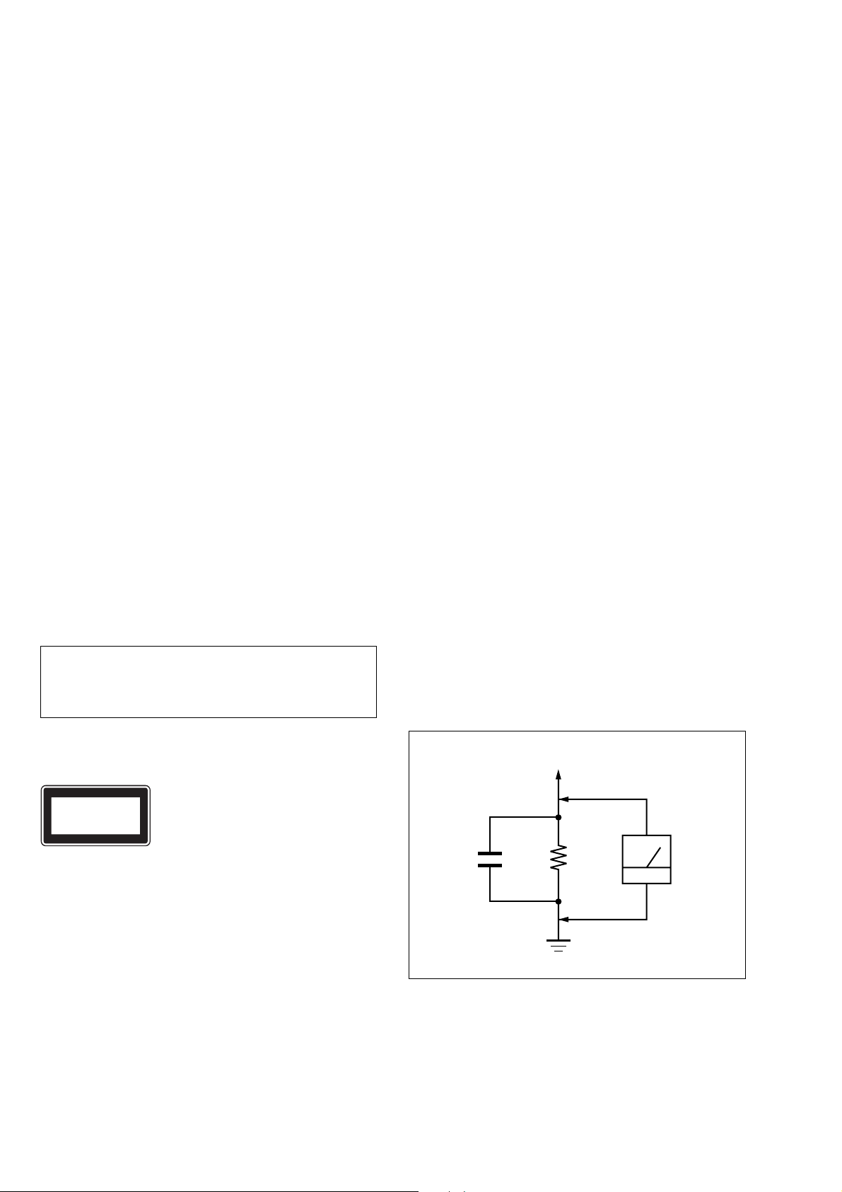
LEAKAGE TEST
The AC leakage from any exposed metal part to earth ground and
from all exposed metal parts to any exposed metal part having a
return to chassis, must not exceed 0.5 mA (500 microamperes.).
Leakage current can be measured by any one of three methods.
1. A commercial leakage tester, such as the Simpson 229 or RCA
WT-540A. Follow the manufacturers’ instructions to use these
instruments.
2. A battery-operated AC milliammeter. The Data Precision 245
digital multimeter is suitable for this job.
3. Measuring the voltage drop across a resistor by means of a
VOM or battery-operated AC voltmeter. The “limit” indication
is 0.75 V, so analog meters must have an accurate low-voltage
scale. The Simpson 250 and Sanwa SH-63Trd are examples
of a passive VOM that is suitable. Nearly all battery operated
digital multimeters that have a 2 V AC range are suitable. (See
Fig. A)
The following caution label is located inside the unit.
This appliance is classified
CLASS 1 LASER PRODUCT
LUOKAN 1 LASER LAITE
KLASS 1 LASER APPARAT
as a CLASS 1 LASER
product.
This label is located on the
rear exterior.
SAFETY CHECK-OUT
After correcting the original service problem, perform the following
safety check before releasing the set to the customer:
Check the antenna terminals, metal trim, “metallized” knobs, screws,
and all other exposed metal parts for AC leakage.
Check leakage as described below.
SAFETY-RELATED COMPONENT WARNING!!
COMPONENTS IDENTIFIED BY MARK 0 OR DOTTED LINE
WITH MARK 0 ON THE SCHEMATIC DIAGRAMS AND IN
THE PARTS LIST ARE CRITICAL TO SAFE OPERATION.
REPLACE THESE COMPONENTS WITH SONY PARTS WHOSE
PART NUMBERS APPEAR AS SHOWN IN THIS MANUAL OR
IN SUPPLEMENTS PUBLISHED BY SONY.
To Exposed Metal
Parts on Set
AC
0.15 µF
1.5 k
Ω
voltmete
(0.75 V)
Earth Ground
Fig. A. Using an AC voltmeter to check AC leakage.
ATTENTION AU COMPOSANT AYANT RAPPORT
LES COMPOSANTS IDENTIFIÉS P AR UNE MARQ UE 0 SUR
LES DIAGRAMMES SCHÉMATIQUES ET LA LISTE DES
PIÈCES SONT CRITIQUES POUR LA SÉCURITÉ DE
FONCTIONNEMENT. NE REMPLACER CES COM- POSANTS
QUE PAR DES PIÈCES SONY DONT LES NUMÉROS SONT
DONNÉS DANS CE MANUEL OU D ANS LES SUPPLÉMENTS
PUBLIÉS PAR SONY.
À LA SÉCURITÉ!
2
Page 3

TABLE OF CONTENTS
1. SERVICING NOTES ............................................... 4
2. GENERAL ................................................................... 6
3. DISASSEMBLY
3-1. Disassembly Flow ........................................................... 8
3-2. Cabinet ............................................................................. 8
3-3. Cabinet (Top) Section...................................................... 9
3-4. Base Unit (BU-K7BD81D-G) ......................................... 9
3-5. Front Panel Section ......................................................... 10
3-6. Mechanical Deck (CMAL5Z231) ................................... 10
3-7. MAIN Board .................................................................... 11
3-8. Tuner Unit ....................................................................... 11
4. TEST MODE.............................................................. 12
5. MECHANICAL ADJUSTMENTS ....................... 13
6. ELECTRICAL ADJUSTMENTS ......................... 13
HCD-NEZ3/NEZ5
7. DIAGRAMS
7-1. Block Diagram – CD SERVO Section – ......................... 15
7-2. Block Diagram – MAIN Section – .................................. 16
7-3. Printed Wiring Board – CD Board – ............................... 18
7-4. Schematic Diagram – CD Board – .................................. 19
7-5. Printed Wiring Boards – MAIN Section – ...................... 21
7-6. Schematic Diagram – MAIN Section (1/2) – .................. 22
7-7. Schematic Diagram – MAIN Section (2/2) – .................. 23
7-8. Printed Wiring Board – PANEL Board – ........................ 24
7-9. Schematic Diagram – PANEL Board – ........................... 25
7-10. Printed Wiring Boards – DC Section – ........................... 26
7-11. Printed Wiring Board – AC Board – ................................ 27
7-12. Schematic Diagram – POWER SUPPLY Section – ........ 28
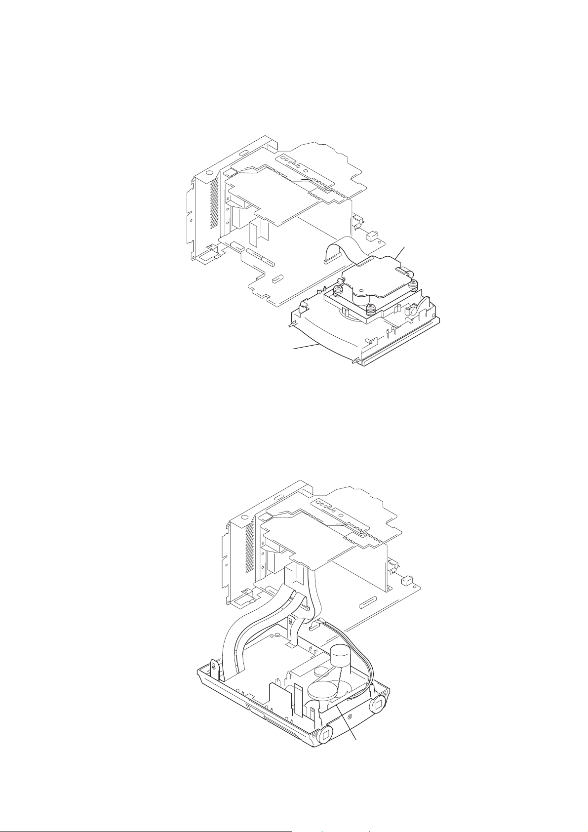
8. EXPLODED VIEWS
8-1. Cabinet Section ................................................................ 35
8-2. Mechanical Deck Section ................................................ 36
8-3. Panel Board Section ........................................................ 37
8-4. Cabinet (Top) Section...................................................... 38
8-5. MAIN Board Section ....................................................... 39
8-6. AC Board, DC Board Section ......................................... 40
9. ELECTRICAL PARTS LIST................................ 41
3
Page 4
HCD-NEZ3/NEZ5
SECTION 1
SERVICING NOTES
NOTES ON HANDLING THE OPTICAL PICK-UP
BLOCK OR BASE UNIT
The laser diode in the optical pick-up block may suffer electrostatic
break-down because of the potential difference generated by the
charged electrostatic load, etc. on clothing and the human body.
During repair, pay attention to electrostatic break-down and also
use the procedure in the printed matter which is included in the
repair parts.
The flexible board is easily damaged and should be handled with
care.
: LEAD FREE MARK
Unleaded solder has the following characteristics.
• Unleaded solder melts at a temperature about 40 ˚C higher
than ordinary solder.
Ordinary soldering irons can be used but the iron tip has to be
applied to the solder joint for a slightly longer time.
Soldering irons using a temperature regulator should be set to
about 350 ˚C.
Caution: The printed pattern (copper foil) may peel away if
the heated tip is applied for too long, so be careful!
• Strong viscosity
Unleaded solder is more viscou-s (sticky, less prone to flow)
than ordinary solder so use caution not to let solder bridges
occur such as on IC pins, etc.
• Usable with ordinary solder
It is best to use only unleaded solder but unleaded solder may
also be added to ordinary solder.
NOTES ON LASER DIODE EMISSION CHECK
The laser beam on this model is concentrated so as to be focused on
the disc reflective surface by the objective lens in the optical pickup block. Therefore, when checking the laser diode emission,
observe from more than 30 cm away from the objective lens.
UNLEADED SOLDER
Boards requiring use of unleaded solder are printed with the leadfree mark (LF) indicating the solder contains no lead.
(Caution: Some printed circuit boards may not come printed with
the lead free mark due to their particular size)
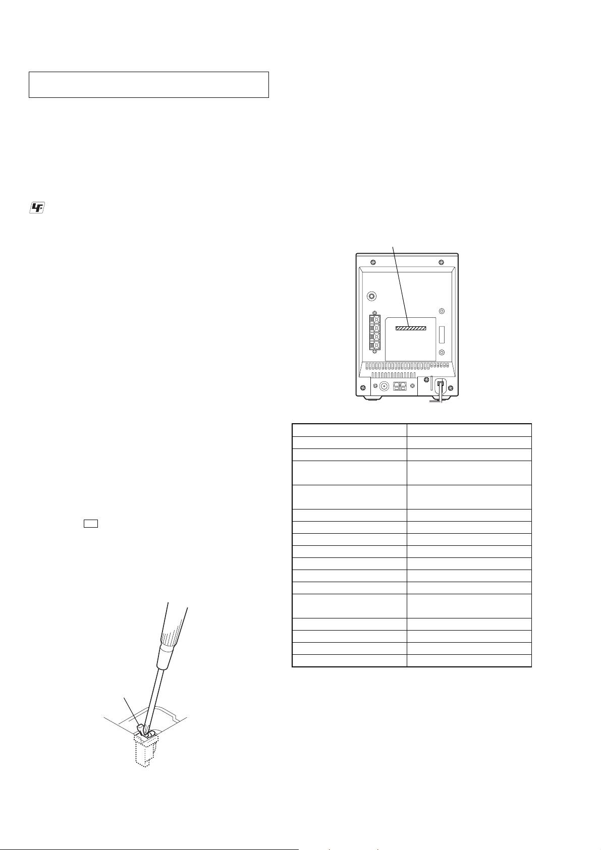
• MODEL IDENTIFICATION
– Rear Cabinet –
Power Voltage Indication
LASER DIODE AND FOCUS SEARCH OPERATION
CHECK
During normal operation of the equipment, emission of the laser
diode is prohibited unless the upper lid is closed while turning ON
the S1820. (push switch type)
The following checking method for the laser diode is operable.
• Method
Emission of the laser diode is visually checked.
1. Open the upper lid.
2. Push the S1820 as shown in Fig.1.
Note: Do not push the detection lever strongly , or it may be bent or damaged.
3. Press the u button.
4. Check the object lens for confirming normal emission of the
laser diode. If not emitting, there is a trouble in the automatic
power control circuit or the optical pick-up.
In this operation, the object lens will move up and down 2
times along with inward motion for the focus search.
S1820
MODEL Power Voltage Incdication
NEZ3: US, CND AC: 120 V 60 Hz 40 W
NEZ3: AEP, UK AC: 230 V - 50/60 Hz 45 W
NEZ3: E, E51, SP
NEZ3: EA
NEZ3: MX ca - 120 V 60 Hz 45 W
NEZ3: TW AC: 120 V - 50/60 Hz 45 W
NEZ3: AR ca - 220 V 50/60 Hz 45 W
NEZ3: KR AC: 220 V - 60 Hz 45 W
NEZ3: AUS AC: 230 − 240 V - 50/60 Hz 45 W
NEZ5: CND AC: 120 V 60 Hz 50 W
NEZ5: AEP, UK AC: 230 V - 50/60 Hz 60 W
NEZ5: E, E51, SP
NEZ5: MX ca - 120 V 60 Hz 50 W
NEZ5: TW AC: 120 V - 50/60 Hz 50 W
NEZ5: AR ca - 220 V 50/60 Hz 50 W
NEZ5: KR AC: 220 V - 60 Hz 50 W
• Abbreviation
AR : Argentina model
AUS: Australian model
CND: Canadian model
E51 : Chilean and Peruvian model
EA : Saudi Arabia model
AC: 120 V/220 V/230 − 240 V
- 50/60 Hz 45 W
AC: 120 − 127 V/220 V/230 − 240 V
- 50/60 Hz 45 W
AC: 120 V/220 V/230 − 240 V
- 50/60 Hz 50 W
KR : Korean model
MX : Mexican model
SP : Singapore model
TW : Taiwan model
Fig.1 Method to push the S1820
4
Page 5
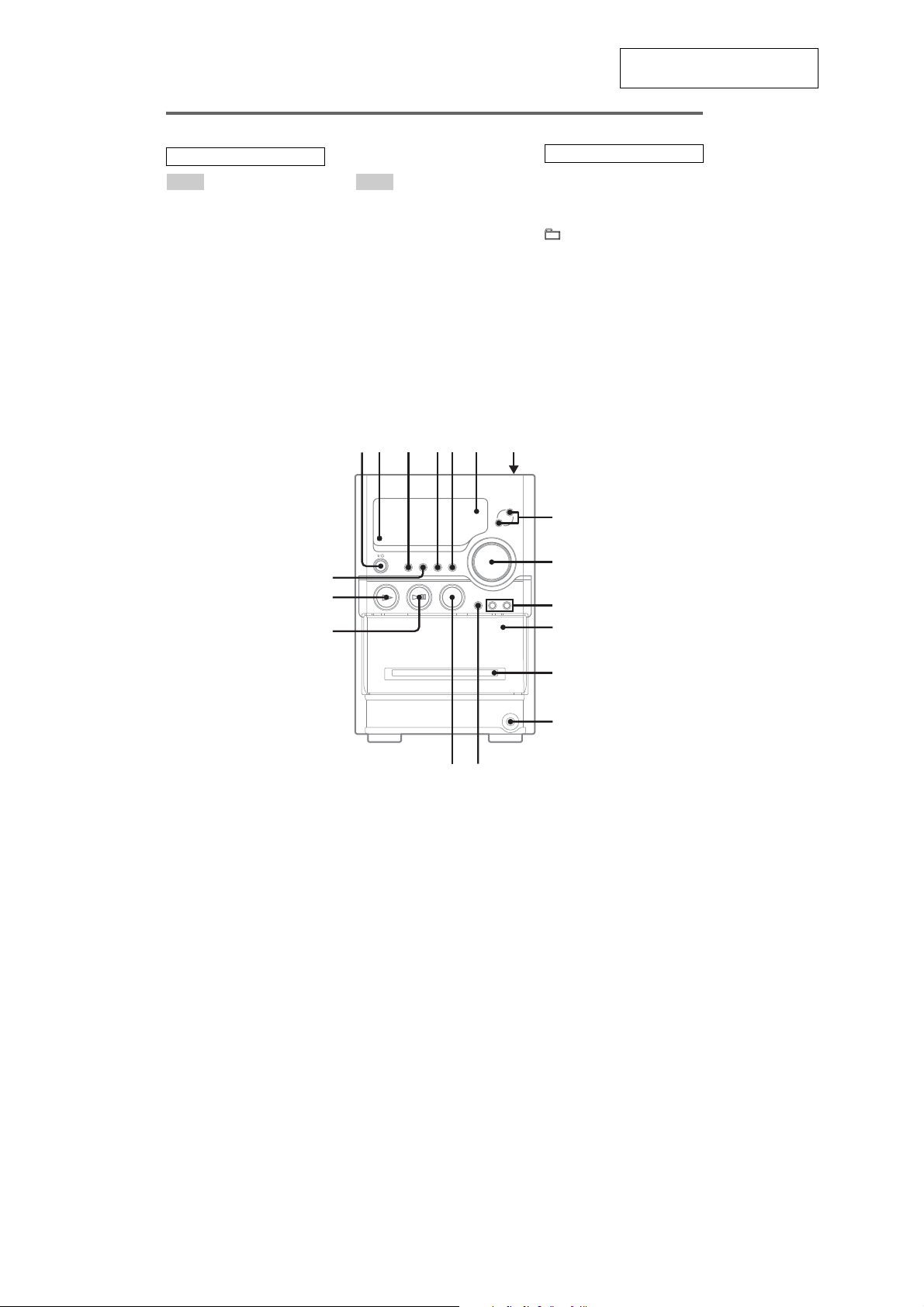
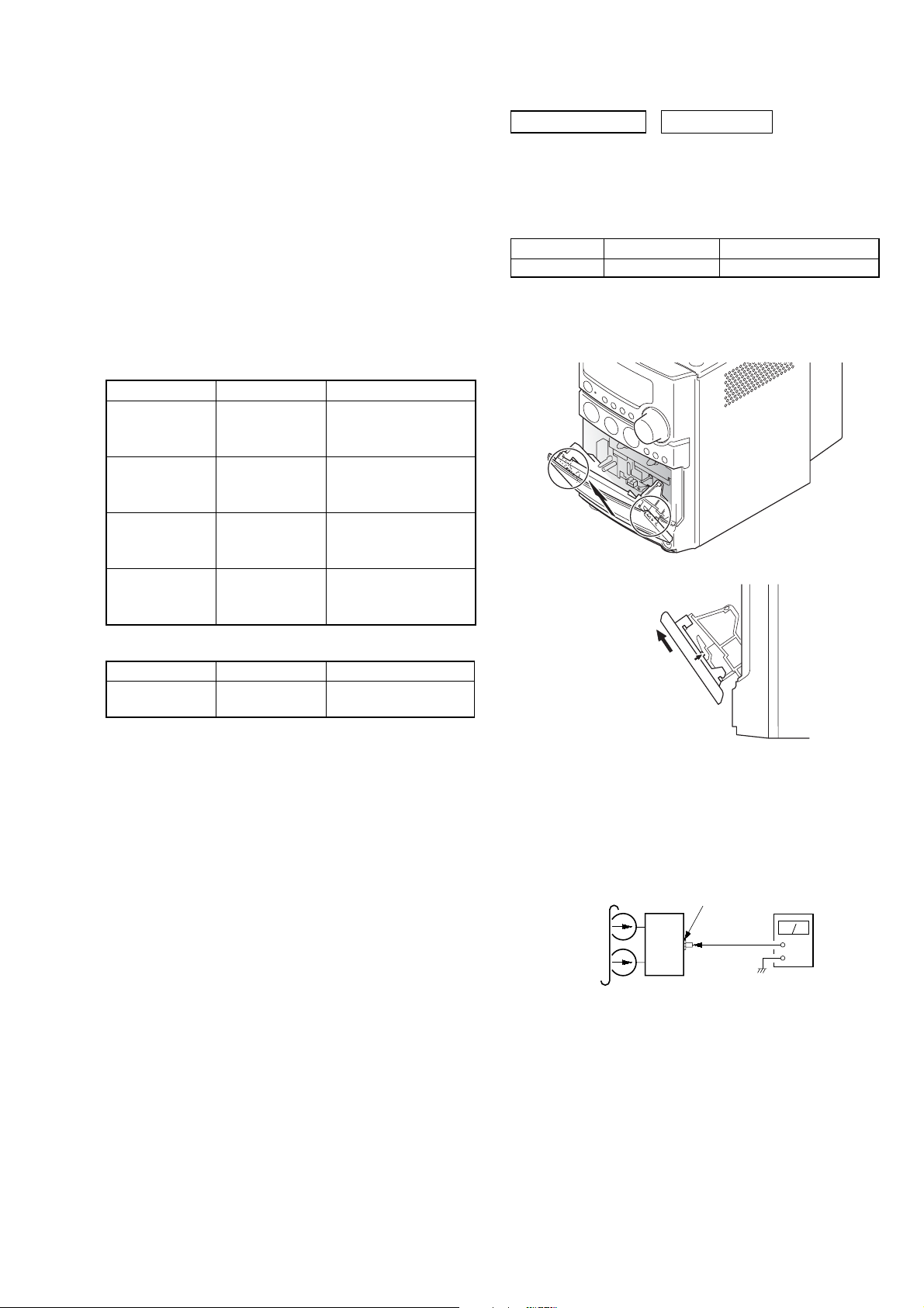
SERVICE POSITION
k
– CD BOARD –
HCD-NEZ3/NEZ5
CD board
– TAPE MECHANICAL DECK –
cabinet (top) section
tape mechanical dec
5
Page 6
HCD-NEZ3/NEZ5
12 3 45 6 7
q
q
Main unit
ALPHABETICAL ORDER
A – S T – Z
CD SYNC qk
Display window 6
DSGX 3
PHONES jack qd
PLAY MODE 5
Remote sensor 2
SECTION 2
GENERAL
Tape deck qs
TUNER/BAND qg
TUNING +/− q;
TUNING MODE 5
VOLUME control 9
This section is extracted from
instruction manual.
BUTTON DESCRIPTIONS
?/1 (power) 1
z PAUSE/START 4
Z PUSH OPEN/CLOSE (CD
open/close) 7
+/− 8*
.m/M> (rewind/fast
forward, go back/go forward)
0
PUSH OPEN/CLOSE Z (tape
open/close) qa
x (stop) qf
CD/NX (play) qh
TAPE/N qj
*Except for North American
model CMT-NEZ3
qk
qj
qh
8
9
0
qa
qs
qd
f
g
6
Page 7
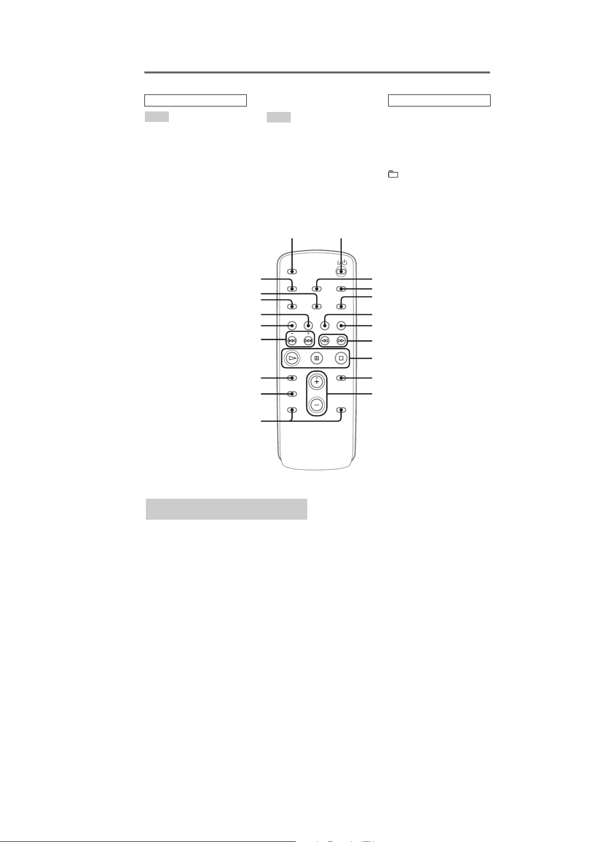
Remote control
HCD-NEZ3/NEZ5
ALPHABETICAL ORDER
A – O
CD qh
CLEAR qd
CLOCK/TIMER SELECT 2
CLOCK/TIMER SET 3
DISPLAY ql
ENTER 9
EQ qs
FM MODE 4
FUNCTION 6
P – Z
PLAY MODE qk
REPEAT 4
SLEEP w;
TAPE qg
TUNER/BAND 5
TUNER MEMORY qj
TUNING MODE qk
VOLUME +/− q;
w;
ql
qk
qj
qh
qg
qf
qd
qs
BUTTON DESCRIPTIONS
?/1 (power) 1
m/M (rewind/fast forward)
7
N (play) 8
X (pause) 8
x (stop) 8
+/− qa
./> (go back/go forward)
qf
−/+ (tuning) qf
1
2
3
4
5
6
7
8
9
0
qa
Setting the clock
Use buttons on the remote for the operation.
1
Press ?/1 to turn on the unit.
2
Press CLOCK/TIMER SET.
3
Press . or > repeatedly to set the
hour.
4
Press ENTER.
5
Press . or > repeatedly to set the
minute.
6
Press ENTER.
The clock starts working.
To adjust the clock
1
Press CLOCK/TIMER SET.
2
Press . or > repeatedly to select
“CLOCK”, then press ENTER.
3
Do the same procedures as step 3 to 6
above.
Note
The clock is not displayed in Power Saving Mode.
7
Page 8
HCD-NEZ3/NEZ5
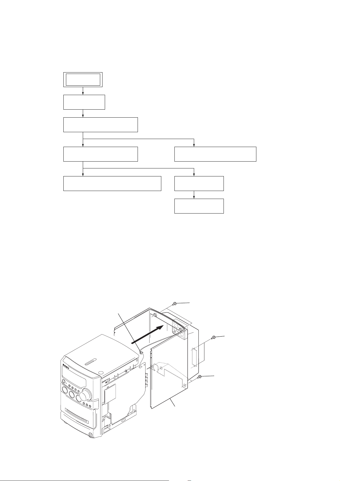
)
• This set can be disassembled in the order shown below.
3-1. DISASSEMBLY FLOW
SET
3-2. CABINET
(Page 8)
3-3. CABINET (TOP) SECTION
(Page 9)
SECTION 3
DISASSEMBLY
3-5. FRONT PANEL SECTION
(Page 10)
3-6. MECHANICAL DECK (CMAL5Z231)
(Page 10)
Note: Follow the disassembly procedure in the numerical order given.
3-2. CABINET
4
fan motor connector
(HCD-NEZ5)
(CN313)
3-4. BASE UNIT (BU-K7BD81D-G)
(Page 9)
3-7. MAIN BOARD
(Page 11)
3-8. TUNER UNIT
(Page 11)
2
two
screws
(BVTP 3
×
10)
3
5
cabinet
1
two
(BVTP 3
2
three
(BVTP 3
screws
screws
×
8)
×
10
8
Page 9
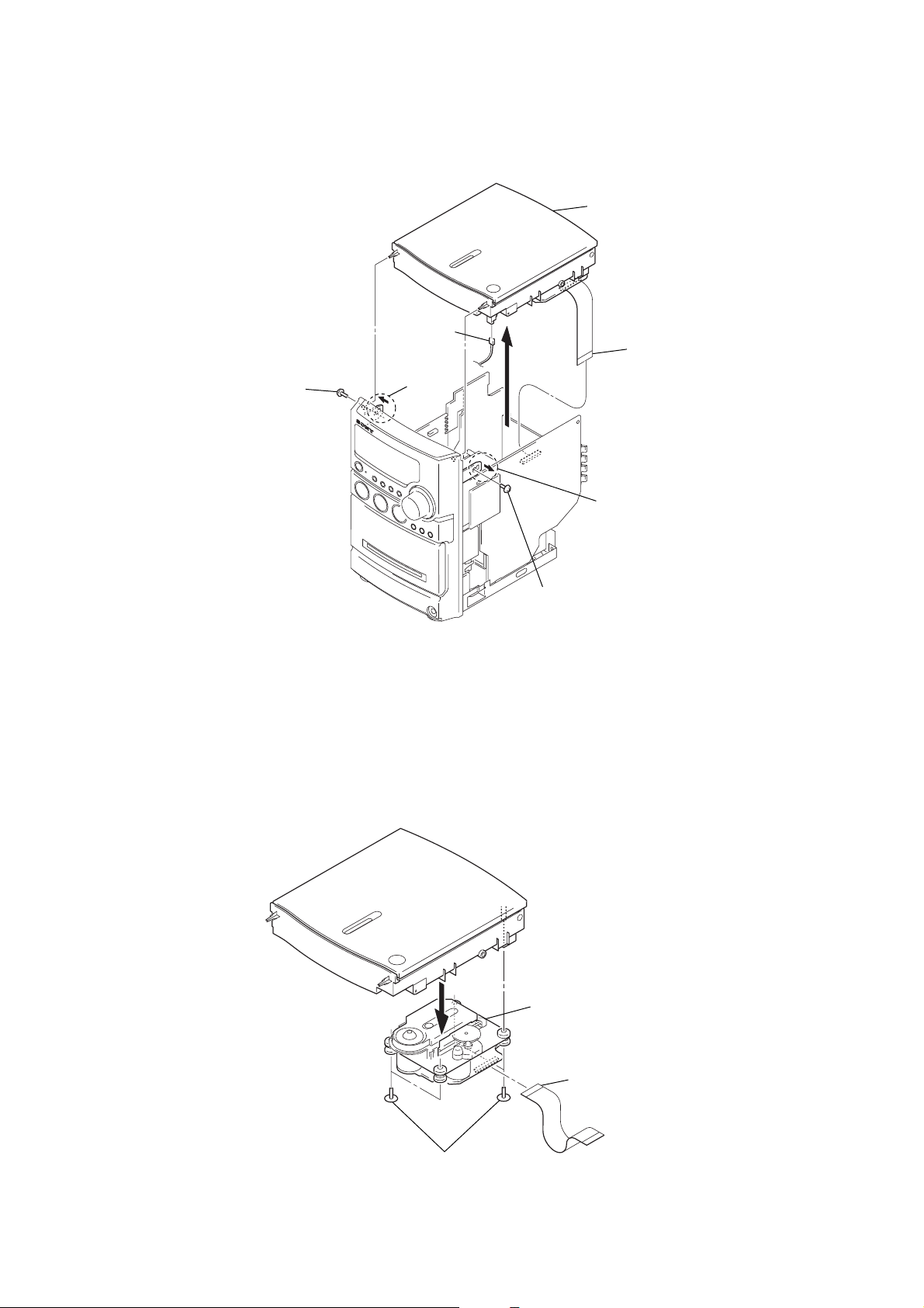
3-3. CABINET (TOP) SECTION
)
1
screw
(BVTP 2.6
×
8)
5
connector
(S1820)
2
claw
3
6
cabinet (top) section
4
wire (flat type) (27 core
(CN317)
HCD-NEZ3/NEZ5
3-4. BASE UNIT (BU-K7BD81D-G)
2
1
screw
(BVTP 2.6
claw
×
8)
2
four
screws
(PWH 2.6
×
10)
3
base unit
(BU-K7BD81D-G)
1
wire (flat type) (27 core)
(CN201)
9
Page 10
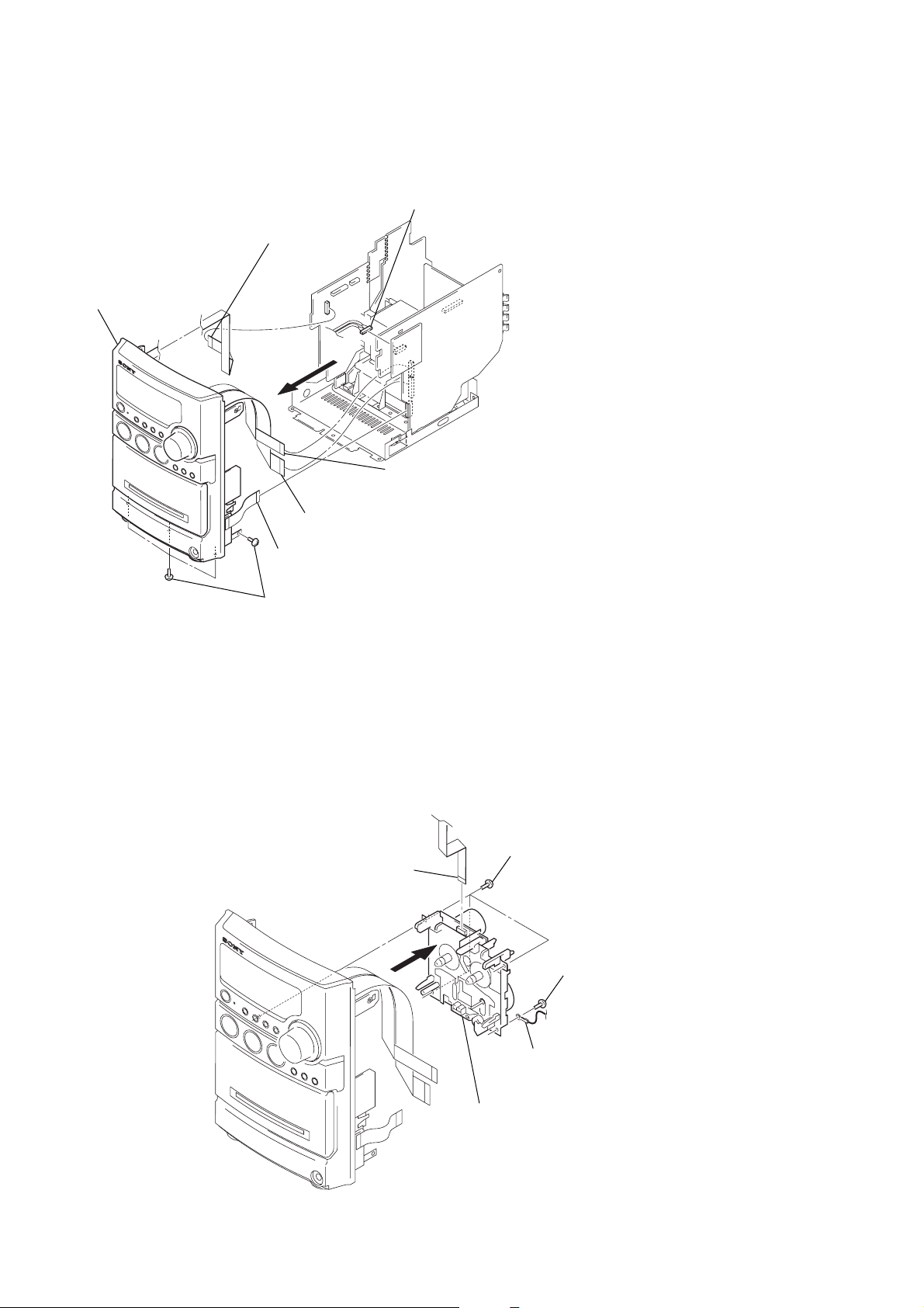
HCD-NEZ3/NEZ5
)
3-5. FRONT PANEL SECTION
4
wire (flat type) (9 core) (FFC1803)
(CN900)
7
front panel section
5
connector
(CN301)
2
wire (flat type) (13 core) (FFC1804) (except NEZ5: AEP, UK models)
wire (flat type) (15 core) (FFC1804) (NEZ5: AEP, UK models)
(CN320)
3
wire (flat type) (19 core) (FFC1805)
(CN321)
1
wire (flat type) (13 core) (FFC501)
(CN500)
6
four
screws
(BVTP 3
×
3-6. MECHANICAL DECK (CMAL5Z231)
1
wire (flat type) (7 core) (FFC1801)
8)
2
three
(BVTP 2.6
screws
×
8)
2
screw
(BVTP 2.6
×
8
10
3
terminal lead wire
(WIRE200)
4
mechanical deck
(CMAL5Z231)
Page 11
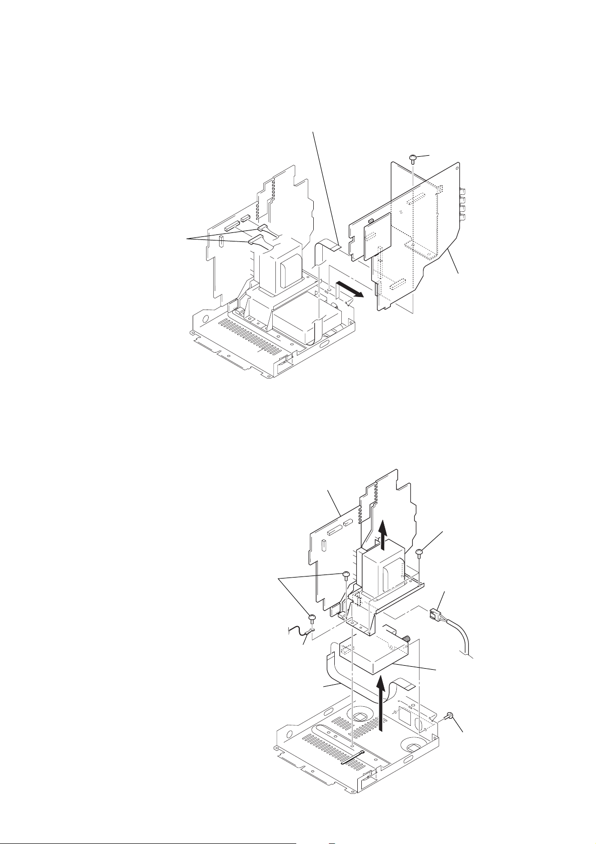
3-7. MAIN BOARD
)
r
1
two connectors
(CN314, CN318)
HCD-NEZ3/NEZ5
4
wire (flat type) (11 core) (except NEZ5: AEP, UK models
wire (flat type) (15 core) (NEZ5: AEP, UK models)
(CN319)
2
screw (BVTP 3
5
MAIN board
3
×
8)
3-8. TUNER UNIT
8
wire (flat type) (11 core) (except NEZ5: AEP, UK models)
wire (flat type) (15 core) (NEZ5: AEP, UK models)
5
AC board, DC board section
1
two
screws
×
(BVTT 3
2
6)
terminal lead wire
(WIRE900)
7
3
1
three
(BVTT 3
4
(CN901)
9
screws
×
6)
power cord connecto
tuner unit
6
two
screws
(BVTP 3
×
8)
11
Page 12
HCD-NEZ3/NEZ5
SECTION 4
TEST MODE
COLD RESET
* The cold reset clears all data including preset data stored in
the RAM to initial conditions. Execute this mode when
returning the set to the customer.
Procedure:
1. Press the I/1 button to turn the power on.
2. While pressing the x button, press the I/1 button and turn
the [VOLUME] knob in the counter-clock wise.
3. The message “RESET” is displayed and the set is reset.
PANEL TEST
* All segments of liquid crystal display are tested, and the version
and released date of the micro computer are displayed.
Procedure:
1. Press the I/1 button to turn the power on.
2. While pressing the [DSGX] button, press the l m button
and turn the [VOLUME] knob in the counter-clock wise.
Then all segments of liquid crystal display are turned on.
3. Press the [DSGX] button, the version and released date of the
micro computer are displayed.
example of display:
1119 V006
Version of micro computer
(In this case, version 006)
released date of micro computer
(In this case, released of November 19)
CD ERROR HISTORY
*This mode can be used for CD error history display.
Procedure:
1. Set the FUNCTION to CD.
2. While pressing the [DSGX] button, press the CD u button
and turn the [VOLUME] knob in the counter-clock wise.
3. CD error history is displayed on the liquid crystal display. Each
time l m or M L button is pressed, CD error history
is changed.
CD POWER MANEGE
*This mode is for switch the CD power supply on/off. Even if
this state pulls out AC plug, it is held.
Procedure:
1. Press the I/1 button to turn the power on.
2. Set the FUNCTION to CD.
3. Press the I/1 button again to turn the power off (standby).
4. While pressing the CD u button, press the I/1 button.
5. If turns power on and display “CD POWER”, then display
“ON” or “OFF”.
4. Press the [TUNER/BAND] button, the model name and
distination are displayed.
example of display:
NE ASIA2
distination
(In this case, Asian model)
model name
(In this case, HCD-NEZXX)
5. Press the [PLAY MODE/TUNING MODE] button, “KEY 0 0” is
displayed on the liquid crystal display, and key test mode in.
Each time a key is pressed, the numerical value corresponding
to each key is displayed on the liquid crystal display.
6. To exit from this mode, perform the “COLD RESET”.
TUNER STEP CHANGE-OVER
* Either the 9 kHz step or 10 kHz step can be selected for the
AM channel step.
Procedure:
1. Set the FUNCTION to AM, and press the
the power off.
2. While depressing the [TUNER/BAND] button, press the I/1 button.
3. The message “9K STEP” or “10K STEP” is displayed on the
liquid crystal display, and thus the channel step is changed
over.
I/1 button to turn
12
Page 13
SECTION 5
r
MECHANICAL ADJUSTMENTS
HCD-NEZ3/NEZ5
SECTION 6
ELECTRICAL ADJUSTMENTS
• Precaution
1. Clean the following parts with a denatured-alcohol-moistened
swab :
record/playback head pinch roller
erase head rubber belts
capstan idlers
2. Demagnetize the record/playback head with a head
demagnetizer. (Do not bring the head magnetizer close to the
erase head.)
3. Do not use a magnetized screwdriver for the adjustments.
4. After the adjustments, appiy suitable locking compound to
the parts adjusted.
5. The adjustments should be performed with the rated power
supply voltage unless otherwise noted.
• Torque Measurement
Mode Torque Meter Meter Reading
2.95 – 6.86 mN⋅m
FWD CQ-102C (30 – 70 g⋅cm)
(0.42 – 0.97 oz⋅inch)
FWD
Back Tension
FF CQ-201B (more than 60 g⋅cm)
REW CQ-201B (more than 60 g⋅cm)
CQ-102C (1.5 – 5.5 g⋅cm)
0.15 – 5.39 mN⋅m
(0.021 – 0.076 oz⋅inch)
more than 5.89 mN⋅m
(more than 0.83 oz⋅inch)
more than 5.89 mN⋅m
(more than 0.83 oz⋅inch)
0 dB=0.775 VDECK SECTION
1. Demagnetize the record/playback head with a head
demagnetizer.
2. Do not use a magnetized screwdriver for the adjustments.
• Test T ape
Tape Signal Used for
P-4-A063 6.3 kHz, -10 dB Azimuth Adjustment
RECORD/PLA YBA CK HEAD AZIMUTH ADJUSTMENT
Note: Remove the cover (azimuth) before this adjustment.
• Tape T ension Measurement
Mode Tension Meter Meter Reading
FWD CQ-403A
more than 100 g
(more than 3.53 oz)
Procedure:
1. Mode: Playback
test tape
P-4-A063
(6.3 kHz, –10 dB)
HEAD PHONE board
PHONES jack
(J500)
set
level mete
+
–
13
Page 14

HCD-NEZ3/NEZ5
+
–
CD board
TP (RFACO)
TP (VC)
oscilloscope
(DC range)
2. Turn the adjustment screw and check output peaks. If the peaks
do not match for L-CH and R-CH, turn the adjustment screw
so that outputs match within 1dB of peak.
Output
level
within
1dB
L-CH
peak
R-CH
peak
within
1dB
Screw
position
L-CH
peak
Screw
position
R-CH
peak
3. Mode: Playback
test tape
P-4-A063
(6.3 kHz, –10 dB)
HEAD PHONE board
PHONES jack
(J500)
set
oscilloscope
H
V
CD SECTION
Note:
1. CD Block is basically constructed to operate without adjustment.
2. Use YEDS-18 disc (3-702-101-01) unless otherwise indicated.
3. Use an oscilloscope with more than 10 MW impedance.
4. Clean the object lens by an applicator with neutral detergent when the
signal level is low than specified value with the following checks.
5. Check the focus bias check when optical block is replaced.
FOCUS BIAS CHECK
Procedure :
1. Connect the oscilloscope to TP (RF ACO) and TP (VC) on the
CD board.
2. Insert the disc (YEDS-18). (Part No. : 3-702-101-01)
3. Press the CD u button.
4. Confirm that the oscilloscope waveform is as shown in the
figure below. (eye pattern)
A good eye pattern means that the diamond shape (‡) in the
center of the waveform can be clearly distinguished.
waveform of oscilloscope
in phase 45°90°135°180
good
°
wrong
4. After the adjustments, apply suitable locking compound to
the pats adjusted.
Adjustment Location: Record/Playback/Erase Head
• RF signal reference waveform (eye pattern)
VOLT/DIV: 0.2 V (with the 10: 1 probe in use.)
TIME/DIV: 500 ns
1.1
0.2 Vp-p
When observing the eye pattern, set the oscilloscope
for AC range and raise vertical sensitivity.
Checking Location:
– CD BOARD (Conductor Side) –
14
TP (VC)
TP
(RFACO)
Page 15
SECTION 7
DIAGRAMS
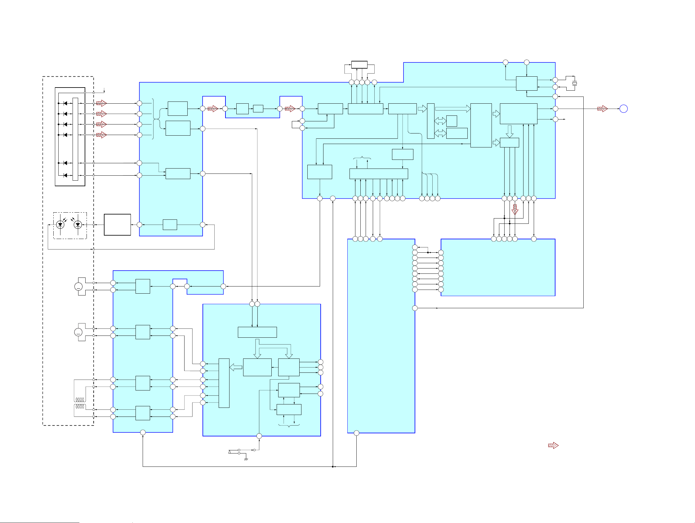
7-1. BLOCK DIAGRAM – CD SERVO Section –
HCD-NEZ3/NEZ5
DETECTOR
A
B
C
D
F
E
OPTICAL PICK-UP
BLOCK
(KSM-213EDP)
LASER DIODE
PD
M101
(SPINDLE)
I-V AMP
LD
M
D +3.3V
AUTOMATIC
POWER
CONTROL
Q10
CH4OUTF
16
CH4OUTR
15
A
26
B
27
C
28
D
29
F
20
E
19
LD
36
MOTOR/COIL DRIVE
IC251
MOTOR
DRIVE
CH4IN
SUMMING
AMP
FOCUS
ERROR
TRACKING
ERROR AMP
APC LD
AMP
24
RF
AMP
FILTER
CD DSP
IC101 (1/2)
AC_
SUM
34
FEO
24
TEO
22
PD
37
OPIN+
OPOUT
27
EQ_
IN
RFAC
35
VCA
2
RFACO
EQ
41
42
45
46
RFACI
ASYI
ASYO
DIGITAL
CLV
PROCESSOR
MDP
6
ASYMMETRY
CORRECTOR
100
XRST
51 53
FILI
PCO
FILO
CLTV
DIGITAL PLL
TO SERVO AUTO
SEQUENCER
CPU INTERFACE
DATA
CLOCK
XLAT
31
33 68
XLT
CDCLK
CDDATA
1125052
XPCK
DEMODULATOR
SUBCODE
PROCESSOR
SQSO
EXCK
SCOR
SENS
SBSO
96 97
98 99115107102 105 104 110 111
SENS
CD SCOR
EFM
SQCK
MP3DI
MP3DO
MP3CLK
MICS
MILP
MIACK
MP3REQ
MP3STB
MP3RST
32K
RAM
INTERNAL BUS
WFCK
XUGF
GFS
113
29
30
28
73
70
72
69
71
75
CORRECTOR
EMPH
68
MIDIO
6
MICK
7
MICS
4
MILP
5
MIACK
8
PO11/BUCK/AD14
36
STANDBY
3
RESET
2
ERROR
MP3 DECODER
IC301
D/A
DIGITAL
INTERFACE
117 93
C4M
SELECTOR
LRCK
63 66 65
16
19
18 14
SBSY/BCKIB
SFSY/LRCKIB
D/A
CONVERTER
BCK
PCMD
15
SDI0
BCKIA
LRCKIA
XTSL
CLOCK
GENERATOR
LRCKI
BCKI
62 60 61
PCMDI
1132 19
SDO0
XTAO
XTAI
XTACN
AOUT1
AOUT2
77
78
95
81
86
R-CH
X171
16.9344MHz
CD
(Page 16)
A
M102
(SLED)
M
2-AXIS
DEVICE
(TRACKING)
(FOCUS)
17
18
14
13
12
11
CH3OUTF
CH3OUTR
CH1OUTF
CH1OUTR
CH2OUTF
CH2OUTR
MOTOR
DRIVE
COIL
DRIVE
COIL
DRIVE
MUTE
20
CH3FIN
CH3RIN
CH1FIN
CH1RIN
CH2FIN
CH2RIN
21 23
CD DSP
IC101 (2/2)
23
21
SFDR
9
SRDR
10
4
5
6
7
TFDR
11
TRDR
12
FFDR
13
FRDR
14
PWM GENERATOR
FOCUS/TRACKING/SLED
S101
(LIMIT)
FEI
TEI
A/D
CONVERTER
FOCUS/
TRACKING/SLED
SERVO DSP
SSTP
7
MIRR,
DFCT, FOK
DETECTOR
SERVO
INTERFACE
SERVO AUTO
SEQUENCER
TO CPU INTERFACE
FOK
MIRR
DFCT
COUT
SCLK
SYSTEM CONTROLLER
IC1801 (1/2)
3
1
2
119
108
XRST
67
XTCN
66
• R-ch is omitted due to same as L-ch.
• SIGNAL PATH
: CD PLAY
HCD-NEZ3/NEZ5
1515
Page 16
HCD-NEZ3/NEZ5
7-2. BLOCK DIAGRAM – MAIN Section –
(Page 15)
ANTENNA
CD
A
FM 75Ω
COAXIAL
AM
HRPE301
(REC/PB/ERASE)
J321
AUDIO IN
FM ANT
ANT GND
AM ANT
ANT GND
L-CH
R-CH R-CH
ERASE
TUNER UNIT
L OUT
R OUT
ST DIN
ST DOUT
ST CLK
TUNED
STEREO
ST MUTE
RDS DATA
RDS INT
(NEZ5: AEP, UK)
ST CE
Q326 – 332
REC/PB
SWITCH
R-CH
R-CH
CLK
TUNED
STEREO
TU-MUTING
RDS DATA
RDS CLOCK
AUX-L
19
18
OUT-L
CD-L
21
R-CH
POWER
AMP
IC501
J500
PHONES
+
ST-L
23
+
DO
DI
CE
TC-L
2
INPUT SELECT,
ELECTRICAL VOLUME
IC302
REC BIAS
SWITCH
Q347, 348
M +10V
CONT
13
RECO-L
+
(NEZ5)
28
D320
DC
DETECT
Q342, 343
D307
D313
–
+
–
FAN MOTOR
DRIVE
Q316, 317
L
R
J302
SPEAKER
IMPEDANCE
USE 6 – 16Ω
M301
(FAN)
MM
• R-ch is omitted due to same as L-ch.
• SIGNAL PATH
: TUNER
: CD PLAY
: TAPE PLAY
: REC
: AUX IN
MAIN POWER
TRANSFORMER
T902
D920, 936
+
BIAS OSC
T301
BIAS OSC
Q344
(NEZ5: AEP, UK)
AC
DETECT
Q333, 338
TO
POWER AMP
AMP B+
AMP B–
RECT
D918, 919
RECT
D916, 917
TAPE MECHANISM
DECK BLOCK
MOTOR
10V
MM
(CAPSTAN/REEL)
(DECK-A)
PLAY SW
END SW
SOL
10V
PACK
REC
CAPSTAN/REEL
MOTOR DRIVE
Q1804, 1805
PLUNGER
DRIVE
Q1802, 1803
LCD1801
LIQUID
CRYSTAL
DISPLAY
REMOTE CONTROL
RECEIVER
IC1802
81
TCMOTOR
80
S0L
94
TC HARF/REC
TCPLAY
78
ENDSW
79
35
LCDDATA
36
LCDCLK
SIRCS
7
DI
DO
CLK
53
51
49
50
DOUT
STDIN
STCLK
LED DRIVE
D1804, 1805
(LCD BACK LIGHT)
CE
TUNED
48
STCE
76
Q1808
STEREO
TU-MUTING
54
55
TUNED
STEREO
STMUTE
BACKLIGHT
RDS DATA
RDS CLOCK
47
18
RDS INT
RDSDATA
LED DRIVE
Q1806
D1806
STANDBY
STBYLED
5
57
56
BIAS
REC/PB
58
SYSTEM CONTROLLER
IC1801 (2/2)
(CD LID OPEN/CLOSE DETECT)
VOLUME
S1801 – 1813
(FRONT PANEL KEYS)
FDATA
X1801
32.768kHz
11 10
XT2
S820
ROTARY
ENCODER
RV1801
15 13
XT1
X1802
10MHz
CF2
60
61
CF1
AMPSTBY
AMPMUTE
77 CD OPEN
97 VOL ENCORDER
74 KEYWAKEUP
KEY0,
KEY1
90, 89
87
CD +1.5V
I POWER MONITOR
65CDON
20ACCUT
12RESET
6POWER ON
REGULATOR
(NEZ5: AEP, UK)
RESET
SWITCH
Q1801
+1.5V
IC303
D +3.3V
RDS +3.3V
D +4V
SYS +3.3V
VOLTAGE
DETECT
IC1803
LCD +3.3V
LCD +4V
B+ SWITCH
Q300, 301
AC DETECT
Q1807
B+ SWITCH
Q1809 – 1811
M +7V
M +10V
A +9V
+3.3V
REGULATOR
D305
D1898
D1809
+7V
REGULATOR
Q320, 321
+10V
REGULATOR
IC900
+9V
REGULATOR
IC902
+4V
REGULATOR
IC901
+4V
REGULATOR
IC903
RECT
D911 – 914
RECT
D907 – 910
D922, 923
SUB POWER
TRANSFORMER
T901
• Abbreviation
E51 : Chilean and Peruvian
EA : Saudi Arabia
SP : Singapore
(EXCEPT E, E51, EA, SP)
(E, E51, EA, SP)
VOLTAGE
SELECTOR
S901
(EXCEPT E, E51, EA, SP)
MAIN POWER
RELAY DRIVE
Q311, 315
RY901
(AC IN)
HCD-NEZ3/NEZ5
1616
Page 17

HCD-NEZ3/NEZ5
/
• Note for Printed Wiring Boards and Schematic Diagrams
Note on Printed Wiring Board:
• X : parts extracted from the component side.
• Y : parts extracted from the conductor side.
f
•
• : Pattern from the side which enables seeing.
(The other layers' patterns are not indicated.)
Caution:
Pattern face side: Parts on the pattern face side seen from
(Conductor Side) the pattern face are indicated.
Parts face side: Parts on the parts face side seen from
(Component Side) the parts face are indicated.
• Indication of transistor
: internal component.
C
B
B
B
Q
E
Q
CE
These are omitted.
Q
CE
These are omitted.
These are omitted.
Note on Schematic Diagram:
• All capacitors are in µF unless otherwise noted. (p: pF)
50 WV or less are not indicated except for electrolytics
and tantalums.
• All resistors are in Ω and 1/
specified.
• f : internal component.
• 2 : nonflammable resistor.
• 5 : fusible resistor.
• C : panel designation.
Note:
The components identified by mark 0 or dotted
line with mark 0 are critical for safety.
Replace only with part
number specified.
• A : B+ Line.
• B : B– Line.
• Voltages and waveforms are dc with respect to ground
under no-signal conditions.
– CD Board –
no mark : CD PLAY
– Other Section –
no mark : TUNER
(): CD PLAY
〈〈 〉〉 : T APE PLAY
{ }: REC
• Voltages are taken with a VOM (Input impedance 10 MΩ).
Voltage variations may be noted due to normal production tolerances.
• Waveforms are taken with a oscilloscope.
Voltage variations may be noted due to normal production tolerances.
• Circled numbers refer to waveforms.
• Signal path.
F : TUNER
J : CD PLAY
E : T APE PLAY
j : REC
f : AUX IN
• Abbreviation
AR : Argentina model
AUS: Australian model
CND : Canadian model
E51 : Chiliean and Peruvian models
EA : Saudi Arabia model
KR : Korean model
MX : Mexican model
SP : Singapore model
TW : Taiwan model
4
W or less unless otherwise
Note:
Les composants identifiés par
une marque 0 sont critiques
pour la sécurité.
Ne les remplacer que par une
pièce portant le numéro
spécifié.
• Circuit Boards Location
TRANS FIXED board
PANEL board
DC board
CONNECT board
HEAD PHONE board
AC board
CD board
MAIN board
SHIELD board
(EXCEPT NEZ3: AEP, UK, Korean
NEZ5: AEP, UK, Korean models)
TUNER UNIT
HCD-NEZ3/NEZ5
1717
Page 18

HCD-NEZ3/NEZ5
7-3. PRINTED WIRING BOARD – CD Section –
1 2 3 4 5 6 7 8 9 10 11 12 13 14 15
A
CD BOARD
(COMPONENT SIDE)
B
C302
C151
R313
C315
C316
R165
C305
C210
C314
X171
C312
R162
R171
R302
C174
R191
R173
C172
R172
C134
C
C303
D
E
FB301
R205
C318
C184
C183
F
R201
G
C201
C203
C182
C209
H
I
• See page 17 for Circuit Boards Location.
R405
R351
R352
R121
C123
R353
C195
C125
C15
C258
C259
C10
C11
C16
Q10
R354
C308
C196
C171
C18
E
C257
C14
R11
C255
R12
R13
R10
: Uses unleaded solder.
C260
R253
C116
C17
1-861-619-
21
(21)
CD BOARD
(CONDUCTOR SIDE)
C252
28 22 1521
IC251
17 148
R252
R251
C251
C114
C113
TP
(VC)
R113
R167
C112
C111
R114
R111
R112
CN101
OPTICAL
PICK-UP
BLOCK
(KSM-213EDP)
C115
C320
M101
M
(SPINDLE)
13
IC303
116
R163
R143
C313
C212
C143
R141
R419
64
49
C142
C311
R409
C211
90
61
R142
C181
C162
54
C141
R306
C194
C161
R403
R408
R412
R203
R401
R406
R151
R301
R402
C213
R182
R161
M102
M
(SLED)
C317
R305
R410
CN201
1
A
MAIN
BOARD
CN317
(Page 21)
21
(21)
R181
C186
C185
R204
27
1-861-619-
C306
17
R307
C307
C309
R411
120 91
1
IC301
32
R303
R407
C163
IC101
30
31 60
C124
C122
C133
R132
TP
(RFACO)
R131
S101
(LIMIT)
R166
R133
R404
C310
4833
C132
C131
HCD-NEZ3/NEZ5
1818
Page 19

HCD-NEZ3/NEZ5
7-4. SCHEMATIC DIAGRAM – CD Section –
C307
R307
0.1
10k
WE/SDO1
SDO2
CS/RAS/
PO12
AD15/CAS/
C314
TP433
MP3VDD
SDO3/OE
PO9/AD12
PO08/AD11
VDDM
SRMSTB
VDDT
AD10
AD9
AD8
PO07/AD7
PO06/AD6
PO05
AD5/
AD4/PO04
47
4V
C311 C309
0.1 0.1
MP3REQ
R303
100k
C310
0.1
FB301
PIO3/IO3
PIO2/IO2
PIO7/BUS3/IO7
PIO6/FI3/BUS2/IO7
AD2/PO02
AD3/PO03
C312C313
0.10.1
C302 C303
0.1 0.1
PIO1/SDI3/IO1
PIO5/FI2/BUS1/IO5
PIO4/FI1/BUS0/IO4
PO11/BUCK/AD14
PO10/CCE/AD13
MP3 DECODER
IC301
TC94A34FG-002
CKO/PO13/AD16
VDD
VSS
AD0/PO00
AD1/PO01
C308
47
4V
GND
STBY
NC
VOUT
C305 TP422
220
4V
VSS
IRQ/FIO
PIO0/SDI2/IO0
VDDX
XO
R306
0
VIN
VDD
CKI/CLOCK/
VSSX
XI
+1.5V REGULATOR
IC303
BH15FB1WG
TXO
TEST
SFSY/LRCKIB
MIMD
MP3GND
• See page 20 for Waveforms. • See page 29 for IC Block Diagrams.
R203
0
SDI1/
DATA
LRCKIA
SBSY/BCKIB
STANBY
VCOI
VSSP
LRCKO
MIACK
MIDIO
RESET
R313
BCKIA
SDI0
BCKO
SDO0
VSS
VDDT
MICK
MILP
MICS
VDDP
220
C316C315
0.00220.1
R351
100
0.1
C306
100
R405
MIACK
100
R404
MICK
MIDIO
100
R419
MILP
100
R403
MICS
100
R402
MP3STB
100
R401
MP3RST
C318
0.01
R301
100k
R305
100k
C317
0.01
R354
100
R352
100
R353
100
10k
R302
C161
0.1
C181
0.1
0
R173
C185
470p
C182
0.1
C186
470p
C201
100
10V
PCMDI
TP427
LRCK
TP103
PCMD
TP104
BCK
TP105
DOUT
R161
100
C171 R171
22p 470
C172
R172
27p
AOUT1
C183
R181
100
6.3V
C184
R182
100
AOUT2
6.3V
C203
C162
100
0.1
10V
1M
22
22
100p
AVSS3
DATA
C133
0.01
R133
180k
R132
10k
VCTL
VPCO
CD DSP
IC101
CXD3059AR
XLAT
VSS
C196
0.1
C131
R131C134
C125 R121
1M0.1
0.1 15k
TP125
RFACI
TP124
RFACO
330p
0.47
C124
C132
BIAS
ASYI
ASYO
RFACI
RFACO
AVDD3
ATSK
SCLK
WFCK
SENS
VDD
CLOCK
R191
0
AVSS4
XUGF
C122C123
0.10.1
LD
PD
NC
RFC
EG_IN
VDD
SCOR
C2PO
GFS
XPCK
AC_SUM
C4M
PDSENS
WDCK
RFDCO
COUT
AVSS0
AVDD0
IOVDD1
IOVSS1
NC
AVDD4
D
C
B
A
VC
FEO
FEI
TEO
TEI
F
E
NC
FRDR
FFDR
TRDR
TFDR
SRDR
SFDR
SSTP
MDP
LOCK
VSS
FOK
DFCT
MIRR
NC
C142
1500p
C143
AVSS5
IOVSS0
0.1
DDVRSEN
XTACN
R162
47k
C210
0.1
C194
0.1
DDVROUT
SQSO
AVDD5
SQCK
R143
3.3k
C141
0.1
R141
4.7k
1k
R142
FILI
PCO
FILO
CLTV
SYSM
XRST
EXCK
SBSO
R166
1k
0.1
100
C163
R163
C151
100
10V
R151
0
BCKI
NC
PCMDI
DDCR
LRCKI
LRCK
VSS
PCMD
BCK
VDD
EMPH
EMPHI
IOVDD2
DOUT
TEST
TEST1
IOVSS2
C174X171
NC
0.116.9344MHz
XVSS
XTAO
XTAI
XVDD
AVDD1
AOUT1
VREFL
AVSS1
AVSS2
VREFR
AOUT2
AVDD2
NC
IOVDD0
RMUT
LMUT
XTSL
NC
R165
0
JPO10 R11
APC 0
R111
JPO102
R113
JPO103
TP425
TP432
TP428
TP429
TP430
TP431
TP423
IOP1
C17
220
4V
1k
1k
1000p
R112
R114
SW+
MDP
C18
FEI
TEI
FRDR
FFDR
TRDR
TFDR
C16R12
1100k
Q10
2SA2119K
AUTOMATIC
POWER
CONTROL
15k
15k
R13
R10
3.3
C111
C112
C113
C114
C115
0.1
C10
C15
10
1
TP424
IOP2
D
C
B
A
3300p
470p
3300p
470p
F
E
FRDR
FFDR
TRDR
TFDR
SRDR
SFDR
MDP
0.1
E
C11
10
D
A
B
C
F
TP102
F+
C14
0.1
C116
C195
0.1
F-
100
10V
VC
TP177
VC
VCC
E
TP10
E
D
TP11
D
A
TP12
A
B
TP13
B
C
TP14
C
F
F
AGND
LD
VR
PD
TP15
PD
F+
TP16
F+
F-
TP17
T+
T-
TP18
T-
F-
TP19
F-
CN101
16P
TP426
SW-
S101
(LIMIT)
(Page 22)
HCD-NEZ3/NEZ5
CN201
27P
M+7V
MGND
MGND
MP3STB
MP3REQ
MIACK
MICK
MIDIO
MILP
MICS
MP3(3.3V)
MP3RST
MP3GND
SCOR
SENS
CLK
XLT
DATA
XRST
XTCN
AVDD(3.3V)
ROUT
AGND
LOUT
DGND
DOUT
DVDD(3.3V)
TP402
TP403
TP405
TP186
TP187
TP401
TP404
TP406
TP407
TP408
TP417
TP416
TP415
TP414
TP413
TP412
TP419
TP434
TP410
TP411
TP409
XTACN
XRST
MVDD
MGND
MP3STB
MP3REQ
MIACK
MICK
MIDIO
MILP
MICS
MP3RST
0
R205
SCOR
SENS
CLK
XLT
DATA
XRST
XTCN
AVDD
ROUT
LOUT
DOUT
R204
MP3STB
MP3REQ
MIACK
MICK
MIDIO
MILP
MICS
MP3RST
R411
SCOR
100
R410
100
R409
100
R408
100
R407
100
R406
100
R412
100
XTACN
CLOCK
C212
SENS
22p
XLT
C211
DATA
220p
XRST
AOUT2
AOUT1
DOUT
TP435
C213
22p
C320
0
DVDD
AVDD
AGND
DGND
TP436
TP420
TP421
C209
R201
0.01
R167
100
XLT
SENS
CLOCK
DATA
MDP
MOTOR/COIL
DRIVE
IC251
BA5947FM
SCOR
R253TP418
10kGAIN_SW
JPO004C251R252R251
MDP6800p22k10k
OPIN-
OPIN+
OPOUT
PREVCC
TFDR
SW
OUTVREF
TRDR
CH1FIN
CH4CAPA
CH1RIN
CH4IN
FRDR
FFDR
CH2FIN
CH2RIN
CH3RIN
CH3FIN
SFDR
SRDR
C259
0.1
F+T+T+T-T-
F-
GND
CNF4
POWVCC
CH2OUTF
CH1OUTF
CH1OUTR
CH2OUTR
CH4OUTR
CH4OUTF
CH3OUTF
CH3OUTR
GND
POWVCC
MUTE
The components identified by mark 0 or dotted
line with mark 0 are critical for safety.
Replace only with part number specified.
C258
0.1
C257
0.1
C252
0.1
C255
0.1
C260
220
10V
SP-
TP250
SP+
TP251
SL+
TP252
SL-
TP253
Les composants identifiés par une marque 0 sont
critiques pour la sécurité. Ne les remplacer que
par une pièce portant le numéro spécifié.
M101
(SPINDLE)
M102
(SLED)
1919
Page 20

HCD-NEZ3/NEZ5
• Waveforms
– CD Board – – MAIN Board – – PANEL Board –
IC101 yd (LRCK)
1
(CD PLAY mode)
IC101 yh (BCK)
2
(CD PLAY mode)
1 V/DIV, 200 ns/DIV
IC101 uj (XTAO)
3
(CD PLAY mode)
22.8 µs
1 V/DIV, 10 µs/DIV
4.5 Vp-p
472 ns
4.4 Vp-p
T301 4
qa
(REC mode)
Q344 (Collector)
qs
(REC mode)
12 µs
50 V/DIV, 5 µs/DIV
12 µs
5 V/DIV, 5 µs/DIV
81.6 Vp-p
16.2 Vp-p
IC1801 qa (XT2)
wa
IC1801 qg (CF2)
ws
30.6 µs
2.8Vp-p
1 V/DIV, 10 µs/DIV
3 Vp-p
100 ns
1 V/DIV, 50 ns/DIV
1 V/DIV, 20 ns/DIV
IC101 ra (RFACO)
4
(CD PLAY mode)
200 mV/DIV, 500 ns/DIV
4.5 Vp-p
59 ns
Approx.
800 mVp-p
HCD-NEZ3/NEZ5
2020
Page 21

HCD-NEZ3/NEZ5
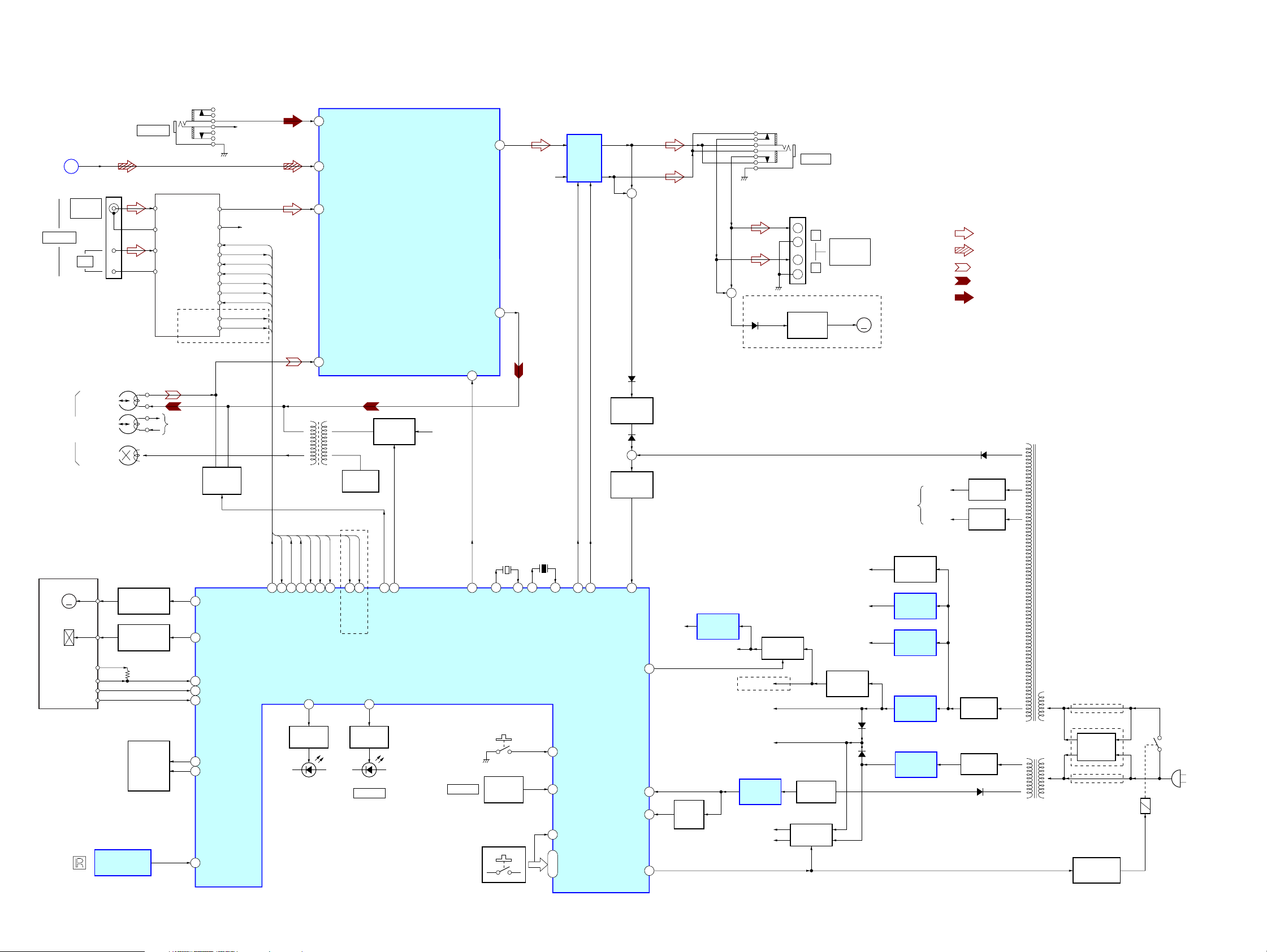
7-5. PRINTED WIRING BOARDS – MAIN Section –
• See page 17 for Circuit Boards Location.
: Uses unleaded solder.
1 2 3 4 5 6 7 8 9 10 11 12 13 14 15 16 17 18 19 20 21 22 23 24
(Page 18)
C330
JW157
JW159JW160
JW161
JW252
C328
FB303
JW233
C326
JW174
C317
JR001
C321
JW224
C322
C325
JW163
JW173
CD BOARD
A
CN201
JW147 JW148
JW144
JW145
JW143
JW142
JW146
CN317
C327
JR004
C307
JR002
JW166
JW167
JW170
JW171
C335
JW117
E
Q300
D305
JW219
Q301
JW225
E
JW226
CN318
JW168
JW190
JW189
11
(11)
JW155
JW156
C138
R304
C308
D325
A/K
18
R386
JW183
TUNER UNIT
SUPPLIED WITH THE
ASSEMBLED BLOCK
FB307
FB305
FB304
C238
C512
C511
R518
C514
KA
JW256
A
B
C
D
E
EXCEPT
NEZ3: AEP, UK, KR/
NEZ5: AEP, UK, KR
F
SHIELD BOARD
G
JW011
JW012
H
I
J
JW013
K
JW014
1-865-200-
11
(11)
L
M
N
J500
O
PHONES
MAIN BOARD
D306
E
R366
C355
C354
Q347
Q348
R367
C361
C362
C358
C356
R362
C304
R310
C314
R309
C303
HEADPHONE BOARD
R534
R532
R530
C521
C520
JW239
JW231
JW238
JW244
E
R533
R531
JW254
JW236
7
L-CH
R368
R525
R519
JW255
T301
JW103
E
Q332
R-CH
HRPE301
(REC/PB/ERASE)
(Page 24)
R528
R526
R520
JW241
R527
R529
(CHASSIS)
Q344
R311
JW235
R201
JW104
Q326
E
Q331
C313
1
ERASE
(Page 24)
1
12
WIRE200
EPT500
R312
R101
R100
C101
R200
C201
E
G
Q328 Q329
F
PANEL
BOARD
D
PANEL
BOARD
1-865-199-
C111
R139
R208
R108
JW105
Q327
JW107
CN301
D
D
G
S
Q330
R319 C312
D302
JW111
FFC501
(CHASSIS)
11
(11)
R138
R114
R249
R112
C211
R111
JW108
JW106
E
17
D
G
S
JW110
R238
R212
C140
R214
R239
C139
JW109
R109
R209
C202
R202
R102
R203
C102
R103
R107
C106
S
R104
C104
C107
(NEZ5: AEP, UK)
CN320
CN500
JW134
C217
R226
R126
C220
R216
C239
CN321
C117
C120
R116
C216
R218
JR152
R217
R247
R117
R248
IC302
C203
R206
C204
C133
R228
C116
R118
R219
R119
R221 R121
R148
R122
C206
R207
R205
JW132
C207
R210
R145
R124
R143
R233
R234
R231
R245
R224
C233
R243
JW113
R149
R211
C240
C103
R105
R106
R204
R110
JW237
R125
R225
JW137
R147
R220
R120
C113
R222
C208
C108
R302
R303
R320
R131
R128
R133
R134
C118
C234
C218
R232
C236
C114
D318
C301
JW218
C214
JW191
C115
JW114
Q321
C136
JW138
C302
C135
R325
JW234
JW151
JW152
JW135
JW136
JW139
R123
R223
R301
JW129
R132
C134
R135
C235
JW215
JW115
R326
E
Q320
R321
JW250
JW214
D326
C213
C305
JW130
JW140
R235
JW116
D321
C215
JW243
JW208
R384
JW249
JW213
R358
JW119
R383
CN319
R382
R381
JW248
Q342
JW217
R380
R378
C329
JW216
JW247
(EXCEPT NEZ5: AEP, UK)
C351
JW207
D307
JW126
K
AA
C309
JW162
JW164
JW165
JW123
C364
R387
JW240
C316
C318
JR003
C311
C310
JW221
D324
R390
(NEZ5: AEP, UK)
C315
R388
JW141
C319
C306
JW176
JW223
1-865-197-
C320
JW158
JW253
JW179
JW188
JW181
JW180
JW232
R389
Q343
E
E
JW133
FB306
JW169
JW177
JW242
JW212
JW121
JW122
C363
D323
R379
R377
JW125
JW220
JW246
JW257
(Page 26)
DC BOARD
B
CN903
JW124
JW149
NEZ3: AEP, UK, EA, KR, AUS/
NEZ5: AEP, UK, KR
C331
14
CN314
JW153
R516
R515
D319
A
A/K
K
A
A/K
R517
K
C513
JW192
JW193
JW198
JW199
JW200
JW185
D320
R521
JW184
R371
JW195
JW196
JW197
JW194
R504
R385
C507
R501
R502
JW230
JW245
JW186
(NEZ5)
C324
JW229
JW187
JW150
R370
R514
R376
R509
C523
C501
M301
M
(FAN)
13
CN313
R328
Q317
Q316
R329
E
K
KA
D327
A/K
JW209
C524
R523
C221
C352
R369
JW204
JW206
R508
R524
C506
R503
NEZ3: AEP, UK, EA, KR, AUS/
C121
JW205
JW210
C353
C505
FB317
C226
E
R318
D313
A
A
R330
R331
JW172
NEZ5: AEP, UK, KR
JW203
R512
R511
R507
JW211
R506
JW251
C370
R237
R236
JW175
R136
C126
L201
L101
JW201
JW202
C516
R137
C119
NEZ3: AEP, UK, EA, KR, AUS/
C227
C127
C219
IC501
C503
DC
BOARD
FM 75Ω
COAXIAL
C
(Page 26)
CN902
ANTENNA
AM
• Semiconductor Location
D302 F-9
D305 H-17
D307 B-15
D313 C-21
D318 F-12
D319 F-18
D320 F-18
D321 J-13
D323 J-14
D324 J-15
D325 G-17
D326 K-13
D327 D-21
IC302 D-11
IC501 J-19
Q300 H-17
(CHASSIS)
NEZ5: AEP, UK, KR
J321
AUDIO IN
+
L
–
J302
SPEAKER
IMPEDANCE
USE 8 – 16Ω
–
R
+
Ref. No. LocationRef. No. Location
Q301 H-16
Q316 C-21
Q317 C-21
Q320 K-13
Q321 J-13
Q326 D-9
Q327 D-10
Q328 E-9
Q329 E-10
Q330 E-9
Q331 E-9
Q332 E-8
Q342 C-14
Q343 B-14
Q344 B-8
Q347 C-7
Q348 C-7
HCD-NEZ3/NEZ5
2121
Page 22

HCD-NEZ3/NEZ5
7-6. SCHEMATIC DIAGRAM – MAIN Section (1/2) –
R236
10k
J321
AUDIO IN
(CHASSIS)
M301
(FAN)
J302
SPEAKER
IMPEDANCE
USE 6-16Ω
(CHASSIS)
(Page 28)
(CHASSIS)
(Page 28)
C370
NEZ3:AEP,UK,EA,KR,AUS/
CN313
3P
FAN+
GND
FAN+
L
R
CN314
4P
+B
GND
-B
GND(CT)
CN318
8P
A+9V
AGND
M+10V
MGND
+UNREG
D+4V
DGND
PROTECT
0.1
NEZ5:AEP,UK,KR
C226 R237
220p 4.7k
C126
R137
220p
4.7k
D327
C121 C221
0.1 0.1
JW229
JW230
LM1876TF
R136
MC2840-T112-1
IC501
10k
(1/2)
C227
470p
C127
470p
FB317
C119
0.01
C219
0.01
NEZ3:AEP,UK,EA,KR,AUS/
NEZ5:AEP,UK,KR
POWER AMP
C501
100p
C523
470p
C505
100p
C524
470p
L101
L201
∗R523,524
0
(NEZ5:AEP,UK)
47
(EXCEPT NEZ3/NEZ5:AEP,UK)
100
(EXCEPT NEZ3:US,CND/NEZ5)
220
(NEZ3;US,CND)
R503 C503
R523
470 47 25V
∗
R504
47k
R505 R506
47k 1k
R524
R508
∗
470
R509
47k
R515 R516
2.2
2W
C511
C512
0.22
0.22
50V
(Page 23)
A8
A7
A6
A5
A4
A3
A2
A1
(EXCEPT NEZ3: US, CND, TW/NEZ5: US, CND, TW)
NEZ3: US, CND, TW/
C330
2200p
NEZ5: US, CND, TW
C308
470
10V
C306
470 10V
C307
470 10V
C328
100p
C326
FB305
22 50V
Q301
RT1N141C-TP-1
R387
10k
R304
4.7k
FB304
C327
100p
C325
100p
C321
100p
C320
100p
C319
C318
100p
C317
22p
C316
100p
C315
100p
C311
100p
C310
100p
C309
FB306
0
XTCN
XRST
DATA
XLT
CLK
SENS
SCOR
MP3REQ
MICK
MILP
MP3STB
MIACK
MID1O
MICS
MP3RST
FB303
100p
470
10V
(NEZ5)
C352
2200
35V
C353
2200
35V
R501
R502
47k
C507
0.1
C506
47
25V
2.2
2W
C513
C514
0.22
0.22
50V
R328
10k
C324
R329
4.7
100k
50V
2SC3052EF
D313
MC2836
R330R331
47k47k
R376
100k
R370
10k
1k
R521 R517
10k 47k
R318
2.2k
Q316
R518
Q317
KTA1273
D319
MC2840-T112-1
R371
10k
C351
100
25V
R369 C516
10k 100
16V
C331
0.01
NEZ3:AEP,UK,EA,KR,AUS/
NEZ5:AEP,UK,KR
MC2840-T112-1
47k
470 1/2W
1K 1/2W
(EXCEPT NEZ3:US,CND/NEZ5)
100 1/2W
(EXCEPT NEZ3/NEZ5:AEP,UK)
220 1/2W
470 1/2W (NEZ3:US,CND,/MEZ5:AEP,UK)
FAN MOTOR DRIVE
Q343
2SC3052EF
R358
47k
R507
10k
R385 R386
∗∗
D320
∗
R385
(NEZ3:US,CND)
(EXCEPT NEZ3:US,CND)
∗
R386
C138
22
50V
Q316,317
Q342,343
DC DETECT
Q342
2SA1235TP-1EF
R511
22k
R512
22k
UDZSTE-174.7B
Q320,321
+7V REGULATOR
R514
10k
AMPSTBY
AMPMUTE
D307
MC2836
D325
MC2840-T112-1
Q321
50V
4.7
C329
C364
2SC3052
10
50V
2SD2012
D324
R321
470
1/2W
Q320
R325
4.7k
D326
UDZSTE-174.7B
D321
1SS355TE-17
R389
10k
R388
10k
10V
22k
2200
C335
R326
CD-L
CD-R
Q300
RT1P137S
C238
XTCN
XRST
DATA
XLT
CLK
SENS
SCOR
MP3RST
MICS
MILP
MID1O
MICK
MIACK
MP3REQ
MP3STB
Q300,301
B+SWITCH
C363
10 50V
D323
UDZ-TE-17-4.7B
R390
100k
R377 R379 R381 R383
470 470 470 220
R378 R380 R382 R384
470 470 470 220
D305
1N4002B
FB307
0
FB307
100p
C322
100p
CN321
19P
DVDD(3.3V)
DOUT
DGND
LOUT
AGND
ROUT
AVDD(3.3V)
XTCN
XRST
DATA
XLT
CLK
SENS
SCOR
MP3GND
MP3RST
MP3(3.3V)
MICS
MILP
MIDIO
MICK
MIACK
MP3REQ
MP3STB
MGND
MGND
M+7V
BDGND
CDON
XTCN
XRST
DATA
XLT
CLK
SENS
SCOR
LEDGND
LED+7V
MP3REQ
MICK
MILP
MP3STB
MIACK
MIDIO
MICS
MP3RST
HP-L
HP-L
HP-L
HP-R
HP-R
HP-R
HPGND
SP-L
SP-L
SP-L
SP-R
SP-R
SP-R
CN500
CN317
13P
27P
(Page 19)
(Page 25)
A9
A10
A11
A12
A13
(Page 23)
(Page 23)
HCD-NEZ3/NEZ5
2222
Page 23

HCD-NEZ3/NEZ5
7-7. SCHEMATIC DIAGRAM – MAIN Section (2/2) –
R135 R235 C235
ANTENNA
FM 75Ω
COAXIAL
100k 100k 10
A5
A4
A8
A1
A2
A7
(Page 22)
(Page 25)
TUNER UNIT
SUPPLIED WITH
THE ASSEMBLED
AM
BLOCK
A3
A6
13P
(EXCEPT NEZ5:AEP,UK)
15P
(NEX5:AEP,UK)
AMPSTBY
AMPMUTE
TAMUTE
FDATA
REC/PB
BIAS
ST MUTE
STEREO
DO(ST->UCOM)
ST CLK
DI(ST<-UCOM)
ST CE
TUNED
RDS DATA
RDS INT
RDS DATA
RDS INT
NC
RDS+3.3V
ST MUTE
R OUT
AGND
L OUT
STEREO
TUNED
+9V
ST CE
ST DIN
ST DOUT
ST CLK
11P
15P
CN320
CN319
15P
(EXCEPT NEZ5:AEP,UK)
(NEZ5:AEP,UK)
50V
C135
10
50V
AMPSTBY
AMPMUTE
STMUTE
STEREO
STDOUT
RDSDATA
RDSINT
(NEZ5:AEP,UK)
RDSDATA
RDSINT
STMUTE
C236
C136
STEREO
STDOUT
STCLK
STDIN
TUNED
TUNED
STDIN
STCLK
• See page 20 for Waveforms. • See page 29 for IC Block Diagrams.
(2/2)
STCE
10 50V
10 50V
STCE
R233 C218
0 47000p
C234 C134 R228
0.001 0.001 1k
R232
1k
R243
10k
R245
BASS-R
0
R224
22k
k
0k
10
1
2.2k
9
19
21
1
148
R
R
R
OUT-R
BASS-L
CONT
VEE
VDD
7
2
30
TE-1
10k
R
355
S
1S
318
D
C301
10p
C305
220
10V
C233
0.047
R226
22k
22k
R126
22k
R125
CD-L
CD-R
9
11
13
A
A
12
10
A
A
A
22k
R225
C116 C216
470p 470p
R220
10k
R120
10k
R223
2.2k
C214
0.47
C115
10
50V
C215
10
50V
50V
C213
R222
0.22
50V
ELECTRICAL VOLUME
R123
2.2k
C113
0.22
50V
∗R122,222
100k (NEZ5)
470k (NEZ3)
INPUT SELECT,
IC302
BD3881FV
22k
R147
10k
R118
10k
R218
22k
R247
R121R221
2.2k2.2k
C114
0.47
50V
∗∗
C120 C117
220p 1000p
R234
0
R231
1k
R132
1k
C217 C220
1000p 220p
.2k
2
2.2k
48
117
2
R
R
AUX-L
OUT-L
TRE-L
TRE-R
p
p
00
C302
4700
47
10V
8
20
108
C
C
7k
301
4
R
03
0k
3
1
R
R133
0
R128
1k
R143 R145
10k 0
R249
R216
R116
R149
R217
2.2k
CD-L
AUX-R
GND
50V
207
C
.2
2
VOLI-R
2.2 50V220
C206
0.022
C118
47000p
R134
0
R131
1k
FFC501
R124C133
22k0.047
10k
47k
47k
10k
R238
2.2k
R214
4.7k
p
11
C2
1000
R212
22k
11
2k
2
R2
ST-L
ST-R
CD-R
VOLI-L
C107
C106
R107
NF-R
RECO-R
PBO-L
TC-R
NF-R
PB0-R
3
p
05
0k
2
20
00
1
22
C
R
R105
220k
0.022
100k
R110
R106
4.7k
R204
R210R206R207
1k4.7k100k
47
100
10V
(Page 22)
R138
2.2k
R114
C111
4.7k
1000p
R109
R111
R112
C239 C140
470p 220p
C240
220p
C139R122
470p
R209
4.7k
NF-L
RECO-L
TC-L
NF-L
C103
100p
1k
R104
47
C104C204
100
10V
4.7k
22k
22k
R139
22k
R239
22k
R103
470
R203
470
2200p 47k
R320
4.7k
R368
10k
1
13
Q331
RT1P241C-TP-1
Q332
RT1P241C-TP-1
C202 R202
HP-L
HP-L
HP-L
HP-R
HP-R
HP-R
HPGND
SP-L
SP-L
SP-L
SP-R
SP-R
SP-R
R108
10k
D302
1SS355TE-17
R208
10k
C313
100
16V
R102C102
47k2200p
D306
R527
470
R525
470
R519
470
R520
470
R526
470
R528
470
∗R529,530
(NEZ3:US,CND)100
200 (EXCEPT NEZ3;US,CND/NEZ5:AEP,UK)
470
(NEZ5:AEP,UK)
2SK2158-T2B
2SA1235TP-1EF
2SA1235TP-1EF
0.0047
Q328
Q326
Q327
C304
R309
C314C303
0.014700p
1k
R533
R531
R529
R534
R532
R530
2SK2158-T2B
S
S
2SK2158-T2B
S
R310
4.7k
100
200
470
∗
∗
∗
∗
∗
∗
C520
Q330
Q329
C201
0.001
R201
47k
∗R531-534
(NEZ3:US,CND)
(EXCEPT NEZ3;US,CND/NEZ5)
(NEZ5)
C521
0.01
0.01
C312
220p
R319
1M
Q326-332
REC/PB SWITCH
R200
10k
5
6
T301
BIAS OSC
C361
47
16V
C362
10
50V
R100
R101
(CHASSIS)
10k
47k
34
2
1
J500
PHONES
EPT500
(CHASSIS)
WIRE200
HRPE301
CN301
7P
C101
0.001
R311
4.7
C356
0.001
R362
Q348
KTA1266-GR-AT
22k
C355
0.022
C358
0.01
Q347
REEC BIAS SWITCH
C354
47
16V
RT1N141C-TP-1
R367
2.2k
R366
22k
Q347,348
Q344
KTC3205Y-A
BIAS OSC
R312
4.7
(REC/PB/ERASE)
ERASE
R-CH
L-CH
HCD-NEZ3/NEZ5
(Page 22)
2323
Page 24

HCD-NEZ3/NEZ5
• Semiconductor
Location
Ref. No. Location
D1801 J-8
D1804 D-5
D1805 D-5
D1806 G-11
D1808 H-3
D1809 G-13
D1898 F-13
D1899 G-8
IC1801 E-9
IC1802 F-12
IC1803 H-3
Q1801 G-3
Q1802 J-7
Q1803 J-6
Q1804 I-7
Q1805 I-6
Q1806 G-10
Q1807 C-12
Q1808 E-5
Q1809 C-11
Q1810 C-12
Q1811 C-12
7-8. PRINTED WIRING BOARD – PANEL
1 2 3 4 5 6 7 8 9 10 11 12 13 14
A
PANEL BOARD
B
JW1903
C
S1820
CD LID OPEN/CLOSE
D
DETECT
E
(FOR CHECK)
19
C1833
2
1
8
JW1814
(EXCEPT NEZ3: US, CND)
S1807
+
JW1813
JW1815
JW1819
F
1
CN1805
Q1801
G
H
I
S1801 – 1813
J
K
R1860
R1859
C1828
C1827
43
12
IC1803
R1857
C1826
JW1867
S1813
TUNING +
M L
JW1833
R1831
Section –
JW1904
JW1800
JW1818
S1806
–
R1877
JW1820
JW1816
C1803
D1808
R1842
• See page 17 for Circuit Boards Location.
R1805
JW1828
Q1803
F
1
JW1868
C1818
JW1854
JW1829
R1881
MAIN BOARD
CN320
(Page 21)
FFC1804
(NEZ5: AEP, UK)
R1837
R1838
R1833
JW1856
S1805
PLAY MODE/
TUNING MODE
Q1805
R1851
D
1
RV1801
VOLUME
R1843
R1844
C1830
S1812
TUNING –
l m
MAIN BOARD
CN321
(Page 21)
FFC1805
15
R1701
R1702
R1704
C1801
JW1817
C1804
R1845
R1883
(LCD BACK LICHT)
JW1823
D1804
C1701
D1805
R1703
R1711
JW1905
JW1830
JW1831
JW1832
D1804, 1805
C1702
Q1808
R1869
C1808
JR1817
(NEZ5)
(NEZ5)
JW1825
JW1853
R1882
S1811
x
JW1826
JW1827
JW1894
JW1899
JW1895
JW1896
R1853
R1850
C1834
R1830
JW1892
JW1862
JW1811
R1801
JW1898
JW1843
JR1821
R1804
R1861
C1817
EXCEPT
NEZ3: US, CND
R1876
JW1834
R1847
E
Q1804
R1852
Q1802
E
S1810
TUNER/
BAND
: Uses unleaded solder.
JW1890
R1820
JW1893
R1840
R1802
R1806
R1808
R1807
JW1835
C1832
JR1818
R1836
R1832
R1839
JW1836
D1801
R1892
R1822
R1835
JW1807
JR1805
C1816
R1818
JW1837
JW1841
JW1824
R1824
R1834
JR1822
R1875
S1804
zPAUSE/
START
C1815
JR1827
JW1842
C1829
R1825
IC1801
JW1901
JW1888
D1899
A
R1813
JW1838
R1880
C1864
51
JW1902
K
K
R1814
JW1840
R1874
JW1839
R1707
R1826
R1812
NEZ3: US, CND/
C1861
R1827
JR1832
JR1819
R1811
R1873
EXCEPT
NEZ5: CND
R1815
R1708
C1809
S1809
CD
u
LCD1801
CRYSTAL
DISPLAY
R1828
S1803
CD SYNC
R1709
LIQUID
R1856
NEZ3: AEP, UK
JW1886
R1866
JW1883
R1893
R1894
R1855
X1802
C1823
C1820
X1801
R1823
C1821
R1854
S1802
DSGX
JR1820
EXCEPT
JW1858
R1849
JW1881
1
TAPE MECHANISM
DECK BLOCK
SUPPLIED WITH THE
ASSEMBLED BLOCK
JW1809
R1867
R1889
R1803
C1819
C1822
Q1806
JW1812
R1887
R1888
R1817
JW1889
C1806
FFC1801
R1886
JW1887
JR1836
R1862
R1810
JW1900
JW1859
R1846
R1848
C1859
R1821
R1829
R1816
R1872
C1805
7
JW1848
JW1884
JR1831
JW1808
C1811
D1806
STANDBY
R1871
JW1860
C1860
Q1809
JW1805
JW1806
IC1802
C1810
R1863
R1841
R1884
JR1823
JR1824
C1831
E
JW1821
JW1822
3
R1819
JW1855
JW1861
R1879
S1808
TAPE
Q1810
B
E
Q1811
JW1880
1
JW1852
JW1857
JW1866
E
JW1849
JW1850
JW1897
S1801
R1858
D1809
R1878
R1885
E
Q1807
JW1885
JW1863
1
9
A
JW1864
C1807
A
KK
K
K
JW1865
1-865-205-
D1898
(11)
11
FFC1803
G
DC BOARD
CN900
(Page 26)
HCD-NEZ3/NEZ5
2424
Page 25

HCD-NEZ3/NEZ5
7-9. SCHEMATIC DIAGRAM – PANEL Section –
RT1P241C-TP-1
C1860
10
16V
Q1810
RT1P241C-TP-1
Q1811
RT1N141C-TP-1
D1809
MC2836
D1898
TAPE MECHANISM
DECK BLOCK
SUPPLIED WITH
THE ASSEMBLED
BLOCK
(Page 28)
FFC1803
FFC1801
9
ACDET
D+4V (SUB)
DGND
DGND
D+4V (MAIN)
POWER-ON
I-P MONITOR
MGND
M+10V
1
1
PLAY SW
REC
PACK
MOTOR10V
SOL10V
COM GND
END SW
7
MC2836
C1830
10
16V
R1841
1k
R1854
0
D1806
SLR325VC
-N-T32
STANDBY
Q1806
RT1N141C-TP-1
LED DRIVE
R1849
4.7k
0.01 0.1
C1809
22
16V
D1801
1SS355TE
-17
C1808
47
16V
• See page 20 for Waveforms. • See page 33 for IC Pin Function Description.
Q1809
Q1809-1811
B+SWITCH
C1807
470
51
4V
100
100
R1892
R1824
100k
R1707
50
100
PLUNGER DRIVE
R1846
4.7k
Q1802
Q1802,1803
R1850
1k
49
48
47
R1829
10k
34
33
32
31
R1863
100
R1851
2.2k
R1825
R1826
100
R1827
100
R1828
100
R1893
10k
R1894
10k
R1886
100
R1887
100
R1803
100
REMOTE CONTROL RECEIVER
IC1802
NJL23H400A
VO
G
C1810
0.01
C1811
10 16V
SOL
Q1803
RT1N141C-TP-1
Q1804
KTA1271Y-AT
R1815
1k
4.7k
R1830
4.7k
R1888
R1889
4.7k
C1805
0.1
R1848
4.7k
R1847
4.7k
C1832
0.1
KTA1271Y-AT
DOUT
STCE
TUNED
RDSDATA
XWR
XHOLD
LCDCLK
LCDDATA
CDCLK
SENS
CDDATA
30
R1858
10k
STDIN
STCLK
MP3DO
MP3CLK
MP3DI
100
R1862
28
R1852 R1853
1k 2.2k
Q1804,1805
CAPSTAN/REEL
MOTOR DRIVE
2SC3052EF-T1-LEF
C1859
4.7
16V
545453
100
R1822
STEREO
Q1807
AC DETECT
56
55
STMUTE
RT1N141C-TP-1
BIAS
Q1805
58
57
REC/PB
D1808
1SS355TE-17
R1821
59
606061
10k
R1820
100k
C1815
0.01
R1840
10k
VSS
VDD2
FDATA
TAMUTE
AMPSTBY
AMPMUTE
SYSTEM CONTROLLER
M30620FCPFP
CD SCOR
RDS INT
ACCUT
100
47k
100
10k
R1810
R1817
R1816
R1855
19
18
TCMOTOR
R1831
IC1803
100k
PST3429UL
C1826
0.1
R1819
X1802
10MHz
69
68
67
66
65
100
100
100
100
R1837
R1836
R1834
R1835
XRST
XTCN
CDON
IC1801
VSS1
CF2
VDD1
10k
C1817
0.1
C1822
C1818
470
4V
VOLTAGE
DETECT
73
707071
72
74
100
100
R1832
XLT
CF1
0.01
C1823
22p
1M
100
R1838
MILP
MP3REQ
XT2
RESET
470k
R1856
100
R1839
100
R1833
MP3STB
XT1
100k
R1823
X1801
C1819
47p
C1820C1821
47p220p
R1857
R1801
R1805
MICS
MIACK
VSS
CNVSS
32.768KHz
10k
100
R1802
MP3RST
BACKLIGHT
KEYWAKEUP
POWER ON
SIRCS
STBYLED
R1806 R1861
1k 22k
C1828 R1859
0.1 47k
100
R1804
CD OPEN
I POWER MONITOR
R1808
ENDSW
TCPLAY
TC HARF/REC
VOL ENCORDER
R1807
100
TCMOTOR
2.2K
4.7K
R1860
47k
SOL
22K
100
KEY1
KEY0
DEST
VSS3
VREF
AVCC
∗R1702,1704
∗R1708
220
(NEZ5)
470
(NEZ3)
∗R1708
(NEZ3:AEP,UK/NEZ5:AEP,UK)
(NEZ3:SP,TW,KR,AUS/NEZ5:SP,TW.KR)
(NEZ3:E,E51,MX,AR/NEZ5:E,E51,MX)
47K
(NEZ3:EA)
Q1801
2SC3052EF-T1-LEF
RESET SWITCH
C1827
0.1
4701K(NEZ3)
(NEZ5)
D1899
MC2836
EXCEPT
NEZ3:AEP,UK
C1829
0.01
LCD1801
LIQUID CRYSTAL DISPLAY
C1864
R1866
100
R1867
100
R1869
10k
SOL
TCMOTOR
220k
R1818
C1816
0.01
100
R1813
100
R1814
R1709
10k
∗
R1708
100
R1812
100
R1811
C1834
0.01
EXCEPT
NEZ3:US,CND/
NEZ5:CND
0.01
C1861
0.01
R1885
R1884
2.2k
2.2k
R1878
10k
C1804
S1808 S1809
TAPE CD
RV1801
R1871
10k
VOLUME
C1803
0.01
R1843
10k
R1842
10k
R1845R1844
10k22k
0.01
S1801 S1802 S1803
R1872
1k
D1804,1805
(LCD BACK LIGHT)
C1801
22
16V
D1804
R1701
∗
∗
C1701
R1702
0.01
∗
R1703
(NEZ5)
∗
R1704 C1702
0.01
∗
(NEZ5)
R1711C1806 C1831
∗
Q1808
RT1N141C-TP-1
LED DRIVE
DSGX
R1873 R1874 R1875
2.2k 2.2k 4.7k
R1880
2.2k
C1833
0.01
31
34
33
32
18
47
48
49
50
51
53
55
56
57
58
59
61
65
66
67
31
68
33
32
19
69
28
71
72
D1805
∗
CD SYNC START
S1810
TUNER/BAND
R1881R1879 R1882 R1883
2.2k1k 4.7k 4.7k
30
73
74
∗R1711
100(NEZ5)
220(NEZ3)
SELU2B10A-SLF62(NEZ3)
SELU2WA10C-B56-LF62(NEZ5)
S1804 S1805 S1806 S1807
PAUSE/ PLAY MODE/
S1811
∗D1804,1805
TUNING MODE
R1876 R1877
S1812 S1813
TUNING − TUNING +
(EXCEPT NEZ3:US,CND)
4.7k 10 k
GND
RXD
BUSY
VDD
SCLK
TXD
PGM
RST
(NEZ5:AEP,UK)
RDS DATA
DI(UCOM->ST)
DO(ST->UCOM)
ST MUTE
AMPMUTE
AMPSTBY
− +
OPEN/CLOSE
RDS INT
TUNED
ST CE
ST CLK
STEREO
BIAS
REC/PB
FDATA
TAMUTE
BDGND
LEDGND
LED+7V
MP3REQ
MP3STB
MIACK
MIDIO
MP3RST
CN1804
CN1805
CDON
XTCN
XRST
DATA
SENS
SCOR
MICK
MILP
MICS
2P
GND
8P
XLT
CLK
S1820
CD LID OPEN/
CLOSE DETECT
(FOR CHECK)
1
FFC1804
(Page 23)
15
1
FFC1805
(Page 22)
19
HCD-NEZ3/NEZ5
2525
Page 26

HCD-NEZ3/NEZ5
JW846
JW914
JW915
JW916
JW939
JW928
JW950
JW926
JW923
JW942
JW925
IC900
CN902
CN903
D918
D917
D912
D914
D913
D916
C919
D919
D911
C903
Q311
CN900
D926
D927
D928
IC901
IC902
JW924
JW937
JW922
JW927
JW932
JW943
JW940
JW931
JW946
JW951
JW960
JW930
IC903
JW952
JW953
JW954
JW955
C336
C350
C920
C928
C918
C922
C901
C902
C925
Q333
D322
Q338
R915
R914
R918
Q315
R917
C923
R919
R913
R912
R911
R916
R907
D920
R902
R901
C929
D936
C930
DC BOARD
1-865-202-
11
(11)
JW001
JW002
JW003
JW004
JW006
JW007
JW008
JW009
JW010JW005
CONNECT BOARD
1-865-201-
11
(11)
54321
AC BOARD
K
(EXCEPT NEZ3: US, CND)
EXCEPT
NEZ3: US, CND
54321
AC BOARD
J
(NEZ3: US, CND)
(NEZ3: US, CND)
54321
MAIN POWER
TRANSFORMER
T902
H
AA
K
K
A/K
A
13
13
13
E
E
E
E
K
K
A
1
3
PANEL BOARD
G
MAIN BOARD
CN318
C
MAIN BOARD
CN314
B
4
1
8
1
1 2 3 4 5 6 7 8 9 10 11 12 13 14
A
B
C
D
E
F
G
H
I
J
K
L
• Semiconductor
Location
Ref. No. Location
D322 J-5
D911 G-4
D912 G-4
D913 G-5
D914 G-4
D916 F-10
D917 E-10
D918 F-10
D919 G-10
D920 F-6
D926 G-8
D927 G-7
D928 H-7
D936 G-5
IC900 H-1
IC901 I-8
IC902 G-6
IC903 K-12
Q311 J-7
Q315 J-6
Q333 J-5
Q338 J-6
7-10. PRINTED WIRING BOARDS – DC Section –
• See page 17 for Circuit Boards Location.
: Uses unleaded solder.
(Page 27)
(Page
(Page
27)
27)
(Page 21)
(Page 21)
HCD-NEZ3/NEZ5
(Page 24)
2626
Page 27

HCD-NEZ3/NEZ5
7-11. PRINTED WIRING BOARD – AC Section –
1 2 3 4 5 6 7 8 9 10 11 12 13 14 15
A
B
C
D
E
F
AC BOARD
NEZ3: E, E51, EA, SP/
NEZ5: E, E51, SP
C931
G
JW907
NEZ5: E, E51, SP
EXCEPT NEZ3: E, E51, EA, SP/
JW908
H
LF901
JW912
I
(AC IN)
(NEZ3: US, CND/NEZ5: CND)
CN901
JW913
NEZ3: US, CND/
EXCEPT
NEZ3: E, E51, EA, SP/
NEZ5: E, E51, SP
NEZ3: US, CND/
NEZ5: CND
EXCEPT
NEZ5: CND
• See page 17 for Circuit Boards Location.
D906
RY901
NEZ3: E, E51, EA, SP/
NEZ5: E, E51, SP
JW906
JW917
JW918
NEZ3: E, E51, EA, SP/
NEZ5: E, E51, SP
JW905
NEZ3: AEP, UK, AR, KR, AUS/
NEZ3: E, E51, EA, SP/
EXCEPT
JW904
JW901
EXCEPT
NEZ5: AEP, UK, AR, KR
: Uses unleaded solder.
S901
VOLTAGE
SELECTOR
120Vt220Vt230 – 240V
120 – 127Vt220Vt230 – 240V
NEZ5: E, E51, SP
(NEZ3: AUS)
JW903
JW902
NEZ3: AEP, UK, AR, KR/
NEZ5: AEP, UK, AR, KR
NEZ3: E, E51, SP/
NEZ5: E, E51, SP
(NEZ3: EA)
T902
MAIN POWER
TRANSFORMER
54321
H
(Page 26)
DC
BOARD
JW909
JW911
EXCEPT
NEZ3: E, E51, EA, SP/
NEZ5: E, E51, SP
SUB POWER
TRANSFORMER
T901
JW921
D909
C921
C914
R906
C915
D923
AA
R904
R908
D907
D908
D910
K
R909
R905
D922
JW919
JW920
J
CONNCT
BOARD
(NEZ3: US, CND) (EXCEPT NEZ3: US, CND)
(Page 26) (Page 26)
CONNCT
BOARD
1-865-198-
54321
K
11
(11)
J
K
HCD-NEZ3/NEZ5
WIRE900
(CHASSIS)
R903
(NEZ3: US, CND/NEZ5: CND)
2727
Page 28

HCD-NEZ3/NEZ5
7-12. SCHEMATIC DIAGRAM – POWER SUPPLY Section –
(Page 22)
(Page 25)
(Page 22)
CN903
+B
GND
-B
GND(CT)
CN900
9P
ACDET
D+4V(SUB)
DGND
DGND
D+4V(MAIN)
POWERON
I-P MONITOR
MGND
M+10V
CN902
8P
PROTECT
DGND
D+4V
+UNREG
MGND
M+10V
AGND
A+9V
R906
10k
D909D910
1N4002B1N4002B
D907
1N4002B
JW901
*
NEZ3:US,CND
NEZ5:CND
JW913
JW912
C914
10
50V
D923
MC2838
NEZ3:AEP,UK,AR,KR/
NEZ5:AEP,UK,AR,KR
EXCEPT NEZ3:AEP,UK,AR,KR,AUS/
NEZ5:AEP,UK,AR,KR
LF901
R905
4.7k
R909
1k
NEZ3:E,E51,EA,SP/
NEZ5:E,E51,SP
EXCEPT
NEZ3:US,CND
NEZ5:CND
EXCEPT
C915
(NEZ3:AUS)
JW902
1000 16V
1000 35V
R904
4.7k
R908
1k
0.1
EXCEPT
NEZ3:E,E51,EA,SP/
NEZ5:E,E51,SP
∗C921
(EXCEPT NEZ3:E,E51,EA,SP/NEZ5:E,E51,SP)
(NEZ3:E,E51,EA,SP/NEZ5:E,E51,SP)
T901
SUB POWER
TRANSFORMER
JW909
JW903
JW906
NEZ3:E,E51,EA,SP/
C931
4700p
250V
JW905
JW908
NEZ5:E,E51,SP
NEZ3:E,E51,EA,SP/
NEZ5:E,E51,SP
NEZ3:US,CND
NEZ5:CND
NEZ3:E,E51,EA,SP/
NEZ5:E,E51,SP
EXCEPT
JW907
NEZ3:E,E51,EA,SP/
NEZ5:E,E51,SP
JW911
S901
EXCEPT
RY901
SELSECTOR
R903
2.2M
1/2W
VOLTAGE
120-127V
220V
230-240V
120V
220V
230-240V
JW904
(NEZ3:EA)
NEZ3:E,E51,SP/
NEZ5:E,E51,SP
D906
1SS355TE-17
CN901
2P
(AC IN)
(CHASSIS)
D922
C921
∗
D908
1N4002B
1SS355TE-17
C922
220
10V
OGI
+4V REGULATOR
4P
Q333,338
AC DETECT
IC903
TA7804LS
+4V REGULATOR
TA7804LS
C918
470
6.3V 0.1
KTA1271Y-AT
MAIN POWER
RELAY DRIVE
R917
100k
Q338
RT1N141C-TP-1
C930
0.1
R911
47k
R912
47k
R913
47k
R919
47k
IC901
OGI
C923
D924
D925
D926
1N4002B
D927
1N4002B
D928
1N4002B
Q311
R918
1k
C336 C350
22
50V
Q333
RT1N141C-TP-1
R914R915
4.7k22k
R916
MC2840-T112-1
D322
MC2836
47k
D918
1N5401M
D919
1N5401M
D920
MC2838
D936
C928
100
16V
10
50V
D916
1N5401M
D917
1N5401M
+9V REGULATOR
IC902
TA7809S
OGI
R901
R902
R907
47k
Q315
RT1N141C-TP-1
MAIN POWER
RELAY DRIVE
C901
0.1
C902
0.1
47k
47k
D913
1N4002B
D914 D912
1N4002B 1N4002B
C929 C919
0.01 2200
JW914
1N4002B
25V
D911
C903
0.1
JW915 JW916
C920 C925
100
16V
G
OI
IC900
TA7810S
+10V REGULATOR
0.01
+UNREG(SUB)
MAIN POWER
TRANSFORMER
T9022
ACDET
GND
GND(CT)
RELAY
T902
HCD-NEZ3/NEZ5
The components identified by mark 0 or dotted
line with mark 0 are critical for safety.
Replace only with part number specified.
Les composants identifiés par une marque 0 sont
critiques pour la sécurité. Ne les remplacer que
par une pièce portant le numéro spécifié.
2828
Page 29

• IC Block Diagrams
– CD Board –
IC101 CXD3059AR
MIRR
DFCT
FOK
VSS
LOCK
MDP
SSTP
IOVSS1
SFDR
SRDR
TFDR
TRDR
FFDR
FRDR
IOVDD1
AVDD0
AVSS0
TEO
FEO
1
2
3
4
5
6
7
8
9
10
11
12
13
14
15
16
17
18
NC
19
E
20
F
21
TEI
22
23
FEI
24
25
VC
MIRR
DFCT
FOK
VC
COUT
NC
119
120
SERVO
INTERFACE
PWM
GENERATOR
SERVO
DSP
A/D
CONVERTER
TE
FE
118
WDCK
117
C4M
HCD-NEZ3/NEZ5
WFCK
C2PO
XPCK
SCOR
GFS
114
112
113
VDD
116
115
ATCK
XUGF
110
109
111
108
DIGITAL
CLV
SCLK
SENS
107
VDD
106
105
SERVO
AUTO
SEQUENCER
ERROR
CORRECTOR
XLAT
CLOK
103
104
CPU INTERFACE
VSS
DATA
102
D/A
INTERFACE
SYSM
101
XRST
EXCK
100
99
D/A
COVERTER
32k
RAM
SBSO
96
97
98
95
CLOCK
GENERATOR
DIGITAL OUT
SELECTOR
94
LPF
LPF
91
92NC93
90
RMUT
89
IOVDD0
88
NC
87
AVDD2
86
AOUT2
85
VREFR
84
AVSS2
83
AVSS1
82
VREFL
81
AOUT1
80
AVDD1
79
XVDD
78
XTAI
77
XTAO
76
XVSS
75
NC
74
IOVSS2
73
TES1
72
TEST
71
DOUT
70
IOVDD2
69
EMPHI
68
EMPH
67
VDD
66
BCK
65
PCMD
64
VSS
63
LRCK
LMUT
XTSL
IOVSS0
XTACN
SQSO
SQCK
EFM
47
48
VPCO
VCTL
DEMODULATOR
DIGITAL
PLL
49
51
50
FILO
CLTV
AVSS3
DC/DC
CONVERTER
56
57
AVSS5
DDVRSEN
58
59
DDCR
NC
54
AVDD5
55
DDVROUT
52
53
FILI
PCO
62
LRCKI
61
PCMDI
60
BCKI
26
A
27
B
28
C
29
D
30
NC
31
32
AVDD4
SUM
33
RFDCO
34
PDSENS
AC_SUM
ATT
35
36LD37
EQ_IN
APC
38NC40
PD
SUB CODE
PROCESSOR
ASYNMMETRY
RFACO
CORRECTOR
42
43
RFACI
44
AVDD3
45
BIAS
46
ASYI
ASYO
EQ
AMP
39
41
RFC
AVSS4
29
Page 30

HCD-NEZ3/NEZ5
IC251 BA5947FM-E2
PREVCC
OPOUT
OUTVREF
CH4CAPA
28
26
27
25
24
CH4IN
23
CH3FIN
CH3RIN
22
GND
MUTE
POWVCC
CH3OUTF
CH3OUTR
CH4OUTF
CH4OUTR
20
21
18
19
16
17
15
MUTING
+
–
INTERFACE
–
+
1
2
OPIN–
OPIN+
4
3
SW
CH1FIN
5
CH1RIN
INTERFACE
INTERFACE
6
CH2FIN
7
CH2RIN
VREF
9
VREFIN
10
POWVCC
8
GND
D
11
CH2OUTR
D
D
12
CH2OUTF
D
LEVEL SHIFT
D D
13
CH1OUTR
DD
14
CH1OUTF
30
Page 31

IC301 TC94A34FG-002
33
34
35
36
37
38
39
40
41
42
1
8
43
5762 5861 5663 52 50
47
46
45
44
48
49
25 26 27 28 29 30 31 3217 18 19 20 21 22 23 24
9
10
11
2
3
4
5
6
7
64 55 53 51
12
13
14
15
16
54
SDO2/
/CS/
/RAS
PO12/
AD15/
/CAS
SDO3/
/OE
TXO
DIT
Bus
Switch
BUCK/
PO11/
AD14
/CCE/
PO10/
AD13
PO9/AD12
PO8/AD11
VDDM
General
Input/
Output
Port
Address Calc.
2sets
Y-Pointer
register
C-Pointer
register
CDP
Control
I/F
Sub Code I/F
X-Pointer
register
SRMSTB
VDDT
AD10
AD9
AD8
PO7AD7
PO6/AD6
PO5/AD5
YRAM
4k word
CRAM
4k word
ERAM
4k wordx12k word
x1
CROM
4k word
x9
XRAM
4k word
Timer
Flag
Interrupt
Control
SRAM/DRAM
I/F
SRAM I/F
1k bit
SRAM
X-Bus
Y-Bus
VCO
Timing
Generator
PRAM
4k word
PROM
4k word
x5
40 bit
Instruction
Decoder
Program
Control
MCU I/F
register
XO/X1/X2
Y0/Y1/Y2
MXMYMZ
MAC
A0A1
AXAY
ALU
A2A3
round & limitround & limit
Audio I/F
SBSY/
BCKIB
DATA/
SDI1
LRCKIA
BCKIA
SDI0
LRCKO
BCKO
SDO0
VDDT
VSS
/MIACK/
AD16
/MICK
MIDIO
/MILP
/MICS
STANDBY
/RESET
VDDP
PO4/
AD4
PO3/
AD3
PO2/
AD2
PO0/
AD0
VSS
PO1/
AD1
VDD
VSSP
VCOI
VDDX
TEST
60
VSSX
CKO/
PO13/
AD16
MIMD
59
XI
XO
CKI/CLCK/
IRQ/FI0
VDD
VSS
PIO0/
SDI2/IO0
PIO1/
SDI3/IO1
PIO2/
IO2
PIO3/
IO3
BUS3/FI1/
PIO4/IO4
BUS2/FI2/
PIO5/IO5
BUS1/FI3/
PIO6/IO6
BUS0/
PIO7/IO7
SDO1//WE
SFSY/
LRCKIB
JTAG
I/F
HCD-NEZ3/NEZ5
31
Page 32

HCD-NEZ3/NEZ5
IC303 BH15FB1WG
THERMAL
PROTECTION
OVER CURRENT
+
−
PROTECTION
VOLTAGE
REFERENCE
1
2
VIN
GND
– MAIN Board –
IC302 BD3881FV
CONTROL
BLOCK
3NC4
STBY
5
VOUT
REC1O27REC1N
28
1
2
PB1P3PB2P
PB1N
REC2N25REC2O24INC223INC122INB221INB120INA219INA1
26
VOLUME
VOLUME
4
PB2N
5
PB2O
6
PB1O
7
VOLIN18VOLIN2
OUT117BAS116OUT215BAS2
18
BASS
TREBLE
9
GND
10
TRE1
TREBLE
11
TRE2
BASS
12
LOGIC
CONTROL
VDD
13
CONT
14
VEE
32
Page 33

• IC PIN FUNCTION DESCRIPITION
PANEL BOARD IC1801 M30620FCPFP (SYSTEM CONTROLLER)
Pin No. Pin Name I/O Description
HCD-NEZ3/NEZ5
1 to 4
5
6
7
8 VSS - Ground terminal
9 CNVSS
10 XT1 I Sub system clock input terminal (32.768 kHz)
11 XT2 O Sub system clock output terminal (32.768 kHz)
12
13
14 VSS1 - Ground terminal
15
16
17 18 RDS INT I RDS serial data transfer clock signal input from the tuner unit (NEZ5: AEP, UK models only)
19 CD SCOR
20
21 to 27
-
STBYLED O
POWER ON O
SIRCS I
RESET I
CF1 I
CF2 O
VDD1 -
ACCUT I
-
-
Not used
LED drive signal output terminal for STANDBY indicate
Power relay drive signal output terminal "H": on
Remote control signal input from the remote control receiver
-
Not used
Reset signal input from the reset switch "L": reset For several hundreds msec. after the power
supply rises, "L" is input, then it changes to "H"
Main system clock input terminal (10 MHz)
Main system clock output terminal (10 MHz)
Power supply terminal (+3.3V)
-
Not used
I
Subcode sync (S0+S1) detection signal input from the CD DSP
Power down detection signal input terminal "L": power down, normally : "H"
-
Not used
28 MP3CLK O Serial data transfer clock signal output to the MP3 decoder
29 MP3DI I Serial data input from the MP3 decoder
30 MP3DO O Serial data output to the MP3 decoder
31 CDDATA O Serial data output to the CD DSP
32 SENS I Internal status (SENSE) signal input from the CD DSP
33 CDCLK O Serial data transfer clock signal output to the CD DSP
34 35 LCDDATA O Serial data output to the liquid crystal display
36 LCDCLK O Serial data transfer clock signal output to the liquid crystal display
37 to 40
41
42 to 45
46
47
48
49
50
51
52
53
54
55
-
XHOLD
-
XWR
RDSDATA I RDS serial data input from the tuner unit (NEZ5: AEP, UK models only)
TUNED I Tuning detection signal input from the tuner unit
STCE O Chip enable signal output to the tuner unit
DOUT O Serial data output to the tuner unit
STCLK O serial data transfer clock signal output to the tuner unit
-
STDIN I Serial data input from the tuner unit
STEREO I FM stereo detection signal input from the tuner unit
STMUTE O Tuner muting on/off control signal output to the tuner unit
-
-
-
-
-
-
Not used
Not used
Not used
Not used
Not used
Not used
33
Page 34

HCD-NEZ3/NEZ5
Pin No. Pin Name I/O Description
56 BIAS O
57 REC/PB O
58
59
60 AMPMUTE
61 AMPSTBY O
62 VDD2 -
63
64
65 CDON O
66 XTCN O
67 XRST O
68
69 MP3REQ I
70
71 MP3STB O
72 MIACK I
73
74 KEYWAKEUP I
75 MP3RST O
76 BACKLIGHT O
77
78
79
80 SOL O
81
82 to 86
87
88
89, 90
91, 92
93
94
95
96
97
98 VREF I
99 AVCC -
100
FDATA
TAMUTE O Line muting on/off control signal output terminal Not used
-
VSS - Ground terminal
XLT
MILP
MICS
CD OPEN I CD lid open/close detection switch input terminal
TCPLAY I PLAY switch signal input from the tape mechanism deck
ENDSW I END switch signal input from the tape mechanism deck
TCMOTOR
-
I POWER
MONITOR
-
KEY1, KEY0 I Front panel key input terminal (A/D input)
-
DEST I Model destination setting terminal
TC HARF/REC I Recording-proof claw (forward/reverse) detect switch and cassette in detect switch input terminal
-
VSS3 - Ground terminal
VOL ENCORDER
-
Recording bias on/off selection signal output terminal "H": bias on, "L": bias off
Recording/playback selection signal output terminal "H": playback mode, "L": recording mode
O
Serial data output to the electrical volume
O Tuner muting on/off control signal output to the power amplifier
Standby control signal output to the power amplifier
Power supply terminal (+3.3V)
-
Not used
Power on/off control signal output for the CD mechanism section
Oscillation circuit control signal output to the CD DSP
"H": auto oscillation, "L": oscillation off
Reset signal output to the CD DSP
O
Serial data latch pulse output to the CD DSP
Request signal input from the MP3 decoder
O
Serial data latch pulse output to the MP3 decoder
Standby control signal output to the MP3 decoder
Acknowledge signal input from the MP3 decoder
O
Chip select signal output to the MP3 decoder
Key interruption processing start signal input terminal
Reset signal output to the MP3 decoder
LED drive signal output terminal for LCD back light
Trigger plunger on/off control signal output terminal "H": plunger on
O
Capstan/reel motor on/off control signal output terminal "H": motor on
-
Not used
I
Power monitor input terminal
-
Not used
-
Not used
-
Not used
I Dial pulse input of the rotary encoder (for VOLUME control)
Reference voltage (+3.3V) input terminal
Power supply terminal (+3.3V)
-
Not used
34
Page 35

SECTION 8
EXPLODED VIEWS
HCD-NEZ3/NEZ5
NOTE:
• -XX and -X mean standardized parts, so they
may have some difference from the original
one.
• Color Indication of Appearance Parts
Example:
KNOB, BALANCE (WHITE) . . . (RED)
• Abbreviation
AR : Argentina model
AUS: Australian model
CND : Canadian model
↑↑
Parts Color Cabinet's Color
E51 : Chirean and Peruvian model
EA : Saudi Arabia model
KR : Korean model
8-1. CABINET SECTION
cabinet (top) section
• Items marked “*” are not stocked since they
are seldom required for routine service. Some
delay should be anticipated when ordering
these items.
• The mechanical parts with no reference
number in the exploded views are not supplied.
• Accessories are given in the last of the
electrical parts list.
MX : Mexican model
SP : Singapore model
TW : T aiw an model
(NEZ5)
M301
not supplied
The components identified by mark
0 or dotted line with mark 0 are
critical for safety.
Replace only with part number
specified.
Les composants identifiés par une
marque 0 sont critiquens pour la
sécurité.
Ne les remplacer que par une pièce
portant le numéro spécifié.
#2
(NEZ5)
4
not supplied
#2
AC board,
DC board
section
2
#1
5
3
MAIN board section
2
5
#1
1
#1
mechanical deck section,
PANEL board section
1
Ref. No. Part No. Description Remark
14-247-752-01 FOOT, RUBBER
24-951-620-01 SCREW (2.6X8), +BVTP
32-581-397-01 CABINET (NEZ3: US)
32-581-397-11 CABINET (NEZ3: CND)
32-581-399-01 CABINET (NEZ3: AEP, UK, MX, TW, AR, KR, AUS)
32-581-399-11 CABINET (NEZ3: E, E51, SP)
32-581-399-21 CABINET (NEZ3: EA)
32-581-402-21 CABINET (SILVER)
(NEZ5: CND, AEP, UK, MX, TW, AR, KR)
Ref. No. Part No. Description Remark
3 2-581-402-31 CABINET (WHITE) (NEZ5: KR)
3 2-581-402-41 CABINET (SILVER) (NEZ5: E, E51, SP)
3 2-581-402-51 CABINET (WHITE) (NEZ5: SP)
4 4-671-016-01 SCREW (FAN) (NEZ5)
5 3-485-343-11 CUSHION, CABINET UPPER 10X7X0.3
M301 1-787-103-11 FAN, DC (NEZ5)
#1 7-685-646-79 SCREW +BVTP 3X8 TYPE2 N-S
#2 7-685-647-79 SCREW +BVTP 3X10 TYPE2 N-S
35
Page 36

HCD-NEZ3/NEZ5
8-2. MECHANICAL DECK SECTION
51
PANEL board section
54
53
52
60
55
61
59
not supplied
(EPT500)
HEAD PHONE board
56
56
not supplied
(WIRE200)
58
57
FFC501
Ref. No. Part No. Description Remark
51 X-2048-718-1 LID ASSY, CASSETTE (SILVER)
51 X-2050-327-1 LID ASSY, CASSETTE (WHITE) (NEZ5)
52 4-245-034-01 SPRING (CASSETTE)
53 2-581-395-01 HOLDER (CASSETTE)
54 4-238-631-01 TAPE SPRING
55 1-796-352-71 DECK, MECHANICAL (CMAL5Z231)
56 4-951-620-01 SCREW (2.6X8), +BVTP
57 A-1090-813-A HEAD PHONE BOARD, COMPLETE
(NEZ3: US, CND)
57 A-1090-905-A HEAD PHONE BOARD, COMPLETE (NEZ5: CND)
57 A-1095-915-A HEAD PHONE BOARD, COMPLETE
(NEZ3: AEP, UK, KR)
36
Ref. No. Part No. Description Remark
57 A-1095-924-A HEAD PHONE BOARD, COMPLETE
(NEZ3: E, E51, EA, MX, SP, TW, AR, AUS)
57 A-1095-934-A HEAD PHONE BOARD, COMPLETE
(NEZ5: AEP, UK)
57 A-1095-972-A HEAD PHONE BOARD, COMPLETE
(NEZ5: E, E51, MX, TW, AR, SP)
57 A-1102-061-A HEAD PHONE BOARD, COMPLETE (NEZ5: KR)
58 4-933-134-11 SCREW (+PTPWH M2.6X8)
59 4-224-104-41 DAMPER
60 4-231-841-01 SPRING (HEART CAM-B)
61 4-231-825-01 CAM (B), HEART
FFC501 1-830-584-11 WIRE (FLAT TYPE) (13 CORE)
Page 37

8-3. PANEL BOARD SECTION
103
FFC1803
PANEL board
HCD-NEZ3/NEZ5
106
106
106
104
D1804,
LCD1801
D1805
108
102
101
Ref. No. Part No. Description Remark
101 2-581-385-01 KNOB (VOL) (NEZ3)
101 2-581-385-11 KNOB (VOL) (NEZ5)
102 X-2048-717-1 PANEL ASSY, FRONT (NEZ3: US)
102 X-2048-755-1 PANEL ASSY, FRONT (NEZ3: AEP, UK, E, E51,
EA, MX, SP, TW, AR, KR, AUS)
102 X-2050-120-1 PANEL ASSY, FRONT (SILVER) (NEZ5: AEP, UK)
102 X-2050-205-1 PANEL ASSY, FRONT (SILVER)
102 X-2050-273-1 PANEL ASSY, FRONT (SILVER) (NEZ3: CND)
102 X-2050-326-1 PANEL ASSY, FRONT (WHITE) (NEZ5: SP, KR)
103 A-1095-891-A PANEL BOARD, COMPLETE (NEZ3: US, CND)
103 A-1095-895-A PANEL BOARD, COMPLETE (NEZ3: AEP, UK)
103 A-1095-922-A PANEL BOARD, COMPLETE
103 A-1095-933-A PANEL BOARD, COMPLETE (NEZ5: AEP, UK)
103 A-1095-971-A PANEL BOARD, COMPLETE (for SILVER)
103 A-1098-688-A PANEL BOARD, COMPLETE
103 A-1098-754-A PANEL BOARD, COMPLETE
103 A-1099-172-A PANEL BOARD, COMPLETE (NEZ3: EA)
103 A-1099-813-A PANEL BOARD, COMPLETE (NEZ5: CND)
103 A-1099-837-A PANEL BOARD, COMPLETE (for WHITE)
(NEZ5: CND, E, E51, MX, TW, AR, SP, KR)
(NEZ3: SP, TW, KR, AUS)
(NEZ5: SP, TW, KR)
(NEZ3: E, E51, MX, AR)
(NEZ5: E, E51, MX, AR)
(NEZ5: SP, KR)
105
FFC1804
FFC1801
FFC1805
107
Ref. No. Part No. Description Remark
104 2-581-391-01 PLATE, LIGHT GUIDE
105 2-594-335-01 HOLDER (LCD-C)
106 4-951-620-01 SCREW (2.6X8), +BVTP
107 2-591-582-01 PLATE (FRONT FFC), PROTECTION
108 2-586-988-01 SHEET (LCD), DIFFUSION
D1804 6-501-139-01 LED SELU2B10A-SLF62 (LCD BACK LIGHT)
D1804 6-501-250-01 LED SELU2WA10C-B56-LF62
(LCD BACK LIGHT) (NEZ5)
D1805 6-501-139-01 LED SELU2B10A-SLF62 (LCD BACK LIGHT)
D1805 6-501-250-01 LED SELU2WA10C-B56-LF62
FFC1801 1-830-583-11 WIRE (FLAT TYPE) (7 CORE)
FFC1803 1-830-579-11 WIRE (FLAT TYPE) (9 CORE)
FFC1804 1-830-580-11 WIRE (FLAT TYPE) (15 CORE) (NEZ5: AEP, UK)
FFC1804 1-830-581-11 WIRE (FLAT TYPE) (13 CORE)
FFC1805 1-830-582-11 WIRE (FLAT TYPE) (19 CORE)
LCD1801 1-805-843-11 DISPLAY PANEL, LIQUID CRYSTAL
LCD1801 1-805-843-21 DISPLAY PANEL, LIQUID CRYSTAL
(LCD BACK LIGHT) (NEZ5)
(EXCEPT NEZ5: AEP, UK)
(NEZ3/NEZ5 (WHITE): SP, KR)
(NEZ5 (SILVER): CND, AEP, UK,
E, E51, MX, TW, AR, SP, KR)
(NEZ3)
(NEZ3)
37
Page 38

HCD-NEZ3/NEZ5
8-4. CABINET (TOP) SECTION
151
152
153
156
157
161
162
not supplied
(spindle motor (M101))
S101
154
155
158
159
not supplied
(sled motor (M102))
161
165
S1820
160
(including spindle motor (M101),
sled motor (M102))
159
162
163
164
Ref. No. Part No. Description Remark
151 X-2048-962-1 LID ASSY, CD (WHITE) (NEZ5)
151 X-2050-124-1 LID ASSY, CD (SILVER)
152 1-452-899-11 MAGNET
153 3-019-395-01 PLATE, CHUCKING
154 3-253-143-01 SCREW (B2.6), (+) P TAPPING
155 2-581-393-01 SPRING (CD)
156 4-232-238-01 DAMPER
157 2-581-388-01 CABINET (TOP) (SILVER) (NEZ3: US)
157 2-581-388-11 CABINET (TOP) (SILVER) (EXCEPT NEZ3: US)
157 2-581-388-31 CABINET (TOP) (WHITE) (NEZ5)
158 4-247-493-01 COVER, CD
159 3-931-379-21 RUBBER, VIBRATION PROOF (RED)
38
The components identified by
mark 0 or dotted line with
mark 0 are critical for safety.
Replace only with part number
specified.
Ref. No. Part No. Description Remark
0 160 8-820-221-01 OPTICAL PICK-UP BLOCK KSM-213EDP/C2NP
161 3-931-379-31 RUBBER, VIBRATION PROOF (GREEN)
162 3-921-725-01 SCREW (2.6X10), +PWH
163 1-827-992-11 WIRE (FLAT TYPE) (16 CORE)
164 1-830-585-11 WIRE (FLAT TYPE) (27 CORE)
165 A-1119-080-A CD BOARD, COMPLETE
S101 1-771-853-11 SWITCH, DETECTION (LIMIT)
S1820 1-692-960-11 SWITCH, PUSH (1 KEY)
#3 7-685-534-19 SCREW +BTP 2.6X8 TYPE2 N-S
Les composants identifiés par une
marque 0 sont critiques pour la
sécurité.
Ne les remplacer que par une pièce
portant le numéro spécifié.
(Including spindle motor (M101),
sled motor (M102))
(CD LID OPEN/CLOSE DETECT)
Page 39

8-5. MAIN BOARD SECTION
HCD-NEZ3/NEZ5
not supplied
(WIRE900)
#4
AC board,
DC board section
#4
(NEZ3: EXCEPT US, CND)
210
not supplied
(NEZ5: EXCEPT CND)
210
not supplied
205
#4
206
#1
#1
207
#1
A
A
208
A
#1
204
203
202
MAIN board
#1
not supplied
(EXCEPT NEZ3: AEP, UK, KR/
NEZ5: AEP, UK, KR)
209
(NEZ3: AEP, UK, KR/
NEZ5: AEP, UK, KR)
#1
#1
#1
201
#4
not supplied
not supplied
Ref. No. Part No. Description Remark
201 A-1101-746-A SHIELD BOARD, COMPLETE
(EXCEPT NEZ3: AEP, UK, KR/NEZ5: AEP, UK, KR)
202 A-1095-890-A MAIN BOARD, COMPLETE (NEZ3: US, CND)
202 A-1095-894-A MAIN BOARD, COMPLETE (NEZ3: AEP, UK)
202 A-1095-921-A MAIN BOARD, COMPLETE (NEZ3: SP)
202 A-1095-929-A MAIN BOARD, COMPLETE (NEZ5: CND)
202 A-1095-932-A MAIN BOARD, COMPLETE (NEZ5: AEP, UK)
202 A-1095-970-A MAIN BOARD, COMPLETE
(NEZ5: E, E51, SP, AR)
202 A-1098-686-A MAIN BOARD, COMPLETE (NEZ3: MX)
202 A-1098-752-A MAIN BOARD, COMPLETE (NEZ5: TW)
202 A-1098-904-A MAIN BOARD, COMPLETE (NEZ3: AR)
202 A-1098-933-A MAIN BOARD, COMPLETE (NEZ3: AUS)
202 A-1098-968-A MAIN BOARD, COMPLETE (NEZ3: TW)
202 A-1099-033-A MAIN BOARD, COMPLETE (NEZ3: KR)
202 A-1099-078-A MAIN BOARD, COMPLETE (NEZ3: E, E51)
202 A-1099-170-A MAIN BOARD, COMPLETE (NEZ3: EA)
The components identified by
mark 0 or dotted line with
mark 0 are critical for safety.
Replace only with part number
specified.
Ref. No. Part No. Description Remark
205 1-693-626-11 TUNER UNIT (NEZ5: AEP, UK)
205 1-693-628-11 TUNER UNIT (NEZ3: E, E51, EA, MX, SP, TW,
205 1-693-629-11 TUNER UNIT (NEZ3: AEP, UK, KR/NEZ5: KR)
206 1-769-946-11 WIRE (FLAT TYPE) (11 CORE)
206 1-773-010-11 WIRE (FLAT TYPE) (15 CORE) (NEZ5: AEP, UK)
207 3-703-244-00 BUSHING (2104), CORD
* 207 3-703-571-12 BUSHING (S) (4516), CORD
0 208 1-769-079-41 CORD, POWER (NEZ3: KR/NEZ5: KR)
0 208 1-769-744-81 CORD, POWER (NEZ3: UK, EA/NEZ5: UK)
0 208 1-775-790-71 CORD, POWER (NEZ3: AUS)
0 208 1-827-226-31 CORD, POWER (NEZ3: E, MX/NEZ5: E, MX)
0 208 1-827-597-31 CORD, POWER (NEZ3: TW/NEZ5: TW)
0 208 1-829-387-11 CORD, POWER (NEZ3: AR/NEZ5: AR)
Les composants identifiés par une
marque 0 sont critiques pour la
sécurité.
Ne les remplacer que par une pièce
portant le numéro spécifié.
AR, AUS/NEZ5: E, E51, MX, SP, TW, AR)
(EXCEPT NEZ5: AEP, UK)
(EXCEPT NEZ3: E, MX/NEZ5: E, MX)
(NEZ3: E, MX/NEZ5: E, MX)
202 A-1101-169-A MAIN BOARD, COMPLETE (NEZ5: KR)
202 A-1119-015-A MAIN BOARD, COMPLETE (NEZ5: MX)
203 2-586-961-01 HEAT SINK
204 2-581-392-01 HEAT SINK (NEZ3: US, CND)
204 2-581-392-11 HEAT SINK (NEZ3: AEP, UK, E, E51, EA, MX, SP,
TW, AR, KR, AUS)
204 2-581-392-21 HEAT SINK (NEZ5)
205 1-693-625-11 TUNER UNIT (NEZ3: US, CND/NEZ5: CND)
0 208 1-830-188-11 CORD, POWER
(NEZ3: AEP, E51, SP/NEZ5: AEP, E51, SP)
0 208 1-830-190-11 CORD, POWER (NEZ3: US, CND/NEZ5: CND)
209 2-598-643-01 PLATE (M), SHIELD (NEZ3: AEP, UK, KR/
NEZ5: AEP, UK, KR)
210 2-594-960-31 SPACER (TRANS)
#1 7-685-646-79 SCREW +BVTP 3X8 TYPE2 N-S
#4 7-685-871-01 SCREW +BVTT 3X6 (S)
39
Page 40

HCD-NEZ3/NEZ5
8-6. AC BOARD, DC BOARD SECTION
251
not supplied
(TRANS FIXED board)
DC board
#1
252
253
254
255
T902
256
Ref. No. Part No. Description Remark
251 A-1090-922-A DC BOARD, COMPLETE (EXCEPT NEZ5: AEP, UK)
251 A-1106-494-A DC BOARD, COMPLETE (NEZ5: AEP, UK)
252 2-586-961-11 HEAT SINK
253 A-1101-747-A CONNECT BOARD, COMPLETE (NEZ3: US, CND)
253 A-1101-751-A CONNECT BOARD, COMPLETE
(EXCEPT NEZ3: US, CND)
254 A-1090-924-A AC BOARD, COMPLETE (NEZ3: US, CND)
254 A-1090-970-A AC BOARD, COMPLETE (NEZ3: AEP, UK)
254 A-1090-971-A AC BOARD, COMPLETE (NEZ3: E, E51, SP)
254 A-1090-972-A AC BOARD, COMPLETE (NEZ5: CND)
254 A-1090-977-A AC BOARD, COMPLETE (NEZ5: AEP, UK)
254 A-1090-978-A AC BOARD, COMPLETE (NEZ5: E, E51, SP)
254 A-1098-903-A AC BOARD, COMPLETE (NEZ3: AR)
254 A-1098-932-A AC BOARD, COMPLETE (NEZ3: AUS)
254 A-1098-967-A AC BOARD, COMPLETE (NEZ3: MX, TW)
254 A-1099-032-A AC BOARD, COMPLETE (NEZ3: KR)
254 A-1099-169-A AC BOARD, COMPLETE (NEZ3: EA)
254 A-1101-058-A AC BOARD, COMPLETE (NEZ5: MX, TW)
254 A-1101-132-A AC BOARD, COMPLETE (NEZ5: AR)
The components identified by
mark 0 or dotted line with
mark 0 are critical for safety.
Replace only with part number
specified.
Ref. No. Part No. Description Remark
254 A-1101-168-A AC BOARD, COMPLETE (NEZ5: KR)
255 2-594-960-01 SPACER (TRANSFORMER)
255 2-594-960-11 SPACER (TRANSFORMER)
255 2-594-960-21 SPACER (TRANSFORMER) (NEZ3: US, CND)
256 2-633-205-01 INSULATED PLATE
0 T902 1-443-565-11 TRANSFORMER, POWER (NEZ5: CND)
0 T902 1-443-566-11 TRANSFORMER, POWER (NEZ5: AEP, UK)
0 T902 1-443-567-11 TRANSFORMER, POWER
0 T902 1-443-573-11 TRANSFORMER, POWER (NEZ3: AEP, UK)
0 T902 1-443-574-11 TRANSFORMER, POWER
0 T902 1-443-626-11 TRANSFORMER, POWER (NEZ3: US, CND)
0 T902 1-443-738-11 POWER TRANSFORMER (NEZ3: EA)
#1 7-685-646-79 SCREW +BVTP 3X8 TYPE2 N-S
Les composants identifiés par une
marque 0 sont critiques pour la
sécurité.
Ne les remplacer que par une pièce
portant le numéro spécifié.
(NEZ3: E, E51, EA, SP/NEZ5: E, E51, SP)
(NEZ3: AEP, UK, MX, TW, AR, KR, AUS/
NEZ5: CND, AEP, UK, MX, TW, AR, KR)
(NEZ5: E, E51, MX, TW, AR, SP, KR)
(NEZ3: E, E51, MX, SP, TW, AR, KR, AUS)
40
Page 41

SECTION 9
ELECTRICAL PARTS LIST
HCD-NEZ3/NEZ5
AC CD
NOTE:
• Due to standardization, replacements in the
parts list may be different from the parts
specified in the diagrams or the components
used on the set.
• -XX and -X mean standardized parts, so they
may have some difference from the original
one.
• RESISTORS
All resistors are in ohms.
METAL: Metal-film resistor.
METAL OXIDE: Metal oxide-film resistor.
F: nonflammable
• Abbreviation
AR : Argentina model
AUS: Australian model
CND : Canadian model
Ref. No. Part No. Description Remark Ref. No. Part No. Description Remark
A-1090-924-A AC BOARD, COMPLETE (NEZ3: US, CND)
A-1090-970-A AC BOARD, COMPLETE (NEZ3: AEP, UK)
A-1090-971-A AC BOARD, COMPLETE (NEZ3: E, E51, SP)
A-1090-972-A AC BOARD, COMPLETE (NEZ5: CND)
A-1090-977-A AC BOARD, COMPLETE (NEZ5: AEP, UK)
A-1090-978-A AC BOARD, COMPLETE (NEZ5: E, E51, SP)
A-1098-903-A AC BOARD, COMPLETE (NEZ3: AR)
A-1098-932-A AC BOARD, COMPLETE (NEZ3: AUS)
A-1098-967-A AC BOARD, COMPLETE (NEZ3: MX, TW)
A-1099-032-A AC BOARD, COMPLETE (NEZ3: KR)
A-1099-169-A AC BOARD, COMPLETE (NEZ3: EA)
A-1101-058-A AC BOARD, COMPLETE (NEZ5: MX, TW)
A-1101-132-A AC BOARD, COMPLETE (NEZ5: AR)
A-1101-168-A AC BOARD, COMPLETE (NEZ5: KR)
E51 : Chirean and Peruvian model
EA : Saudi Arabia model
KR : Korean model
*******************
• Items marked “*” are not stocked since they
are seldom required for routine service.
Some delay should be anticipated when
ordering these items.
• SEMICONDUCTORS
In each case, u: µ, for example:
uA... : µA... uPA... : µPA...
uPB... : µPB... uPC... : µPC...
uPD... : µPD...
• CAPACITORS
uF: µF
• COILS
uH: µH
MX : Mexican model
SP : Singapore model
TW : Taiwan model
R906 1-216-833-11 METAL CHIP 10K 5% 1/10W
R908 1-216-821-11 METAL CHIP 1K 5% 1/10W
R909 1-216-821-11 METAL CHIP 1K 5% 1/10W
0 RY901 1-755-276-11 RELAY, POWER
0 S901 1-786-055-21 SELECTOR, VOLTAGE (VOLTAGE SELECTOR)
The components identified by mark
0 or dotted line with mark 0 are
critical for safety.
Replace only with part number
specified.
Les composants identifiés par une
marque 0 sont critiquens pour la
sécurité.
Ne les remplacer que par une pièce
portant le numéro spécifié.
When indicating parts by reference
number, please include the board.
< RELAY >
< SWITCH >
(NEZ3: E, E51, EA, SP/NEZ5: E, E51, SP)
< TRANSFORMER >
< CAPACITOR >
C914 1-126-964-11 ELECT 10uF 20% 50V
C915 1-136-497-81 FILM 0.1uF 5% 50V
C921 1-126-767-11 ELECT 1000uF 20% 16V
(EXCEPT NEZ3: E, E51, EA, SP/NEZ5: E, E51, SP)
C921 1-126-952-11 ELECT 1000uF 20% 35V
(NEZ3: E, E51, EA, SP/NEZ5: E, E51, SP)
0 C931 1-113-924-11 CERAMIC 0.0047uF 20% 250V
< CONNECTOR >
* CN901 1-793-660-11 PIN, CONNECTOR (PC BOARD) 3P
< DIODE >
D906 8-719-988-61 DIODE 1SS355TE-17
D907 8-719-063-79 DIODE 1N4002B
D908 8-719-063-79 DIODE 1N4002B
D909 8-719-063-79 DIODE 1N4002B
D910 8-719-063-79 DIODE 1N4002B
D922 8-719-988-61 DIODE 1SS355TE-17
D923 8-719-000-08 DIODE MC2838
< LINE FILTER >
0 LF901 1-402-663-11 TRANSFORMER, LINE FILTER (LFT)
(EXCEPT NEZ3: US, CND/NEZ5: CND)
< RESISTOR >
0 R903 1-219-512-22 METAL 2.2M 5% 1/2W F
(NEZ3: US, CND/NEZ5: CND)
R904 1-216-829-11 METAL CHIP 4.7K 5% 1/10W
R905 1-216-829-11 METAL CHIP 4.7K 5% 1/10W
0 T901 1-439-772-11 TRANSFORMER, POWER (NEZ3: E, E51, EA, SP,
AR /NEZ5: E, E51, SP, AR)
0 T901 1-439-779-11 TRANSFORMER, POWER
(NEZ3: AEP, UK, KR, AUS/NEZ5: AEP, UK, KR)
0 T901 1-439-781-11 TRANSFORMER, POWER
(NEZ3: US, CND, MX, TW/NEZ5: CND, MX, TW)
*************************************************************
A-1119-080-A CD BOARD, COMPLETE
*******************
< CAPACITOR/JUMPER RESISTOR >
C10 1-165-989-11 CERAMIC CHIP 10uF 10% 6.3V
C11 1-165-989-11 CERAMIC CHIP 10uF 10% 6.3V
C14 1-164-360-11 CERAMIC CHIP 0.1uF 16V
C15 1-164-360-11 CERAMIC CHIP 0.1uF 16V
C16 1-115-156-11 CERAMIC CHIP 1uF 10V
C17 1-126-246-11 ELECT CHIP 220uF 20% 4V
C18 1-162-964-11 CERAMIC CHIP 0.001uF 10% 50V
C111 1-162-967-11 CERAMIC CHIP 0.0033uF 10% 50V
C112 1-164-315-11 CERAMIC CHIP 470PF 5% 50V
C113 1-162-967-11 CERAMIC CHIP 0.0033uF 10% 50V
C114 1-164-315-11 CERAMIC CHIP 470PF 5% 50V
C115 1-164-360-11 CERAMIC CHIP 0.1uF 16V
C116 1-128-995-21 ELECT CHIP 100uF 20% 10V
C122 1-107-826-11 CERAMIC CHIP 0.1uF 10% 16V
C123 1-107-826-11 CERAMIC CHIP 0.1uF 10% 16V
C124 1-162-959-11 CERAMIC CHIP 330PF 5% 50V
C125 1-164-360-11 CERAMIC CHIP 0.1uF 16V
C131 1-162-927-11 CERAMIC CHIP 100PF 5% 50V
C132 1-117-863-11 CERAMIC CHIP 0.47uF 10% 6.3V
C133 1-162-970-11 CERAMIC CHIP 0.01uF 10% 25V
41
Page 42

HCD-NEZ3/NEZ5
CD
Ref. No. Part No. Description Remark Ref. No. Part No. Description Remark
< FERRITE BEAD >
C134 1-164-360-11 CERAMIC CHIP 0.1uF 16V
C141 1-107-826-11 CERAMIC CHIP 0.1uF 10% 16V
C142 1-162-965-11 CERAMIC CHIP 0.0015uF 10% 50V
C143 1-164-360-11 CERAMIC CHIP 0.1uF 16V
C151 1-128-995-21 ELECT CHIP 100uF 20% 10V
C161 1-164-360-11 CERAMIC CHIP 0.1uF 16V
C162 1-164-360-11 CERAMIC CHIP 0.1uF 16V
C163 1-164-360-11 CERAMIC CHIP 0.1uF 16V
C171 1-162-919-11 CERAMIC CHIP 22PF 5% 50V
C172 1-162-920-11 CERAMIC CHIP 27PF 5% 50V
FB301 1-500-445-21 FERRITE, EMI (SMD) (2012)
< IC >
IC101 8-752-425-12 IC CXD3059AR
IC251 6-705-808-01 IC BA5947FM-E2
IC301 6-705-365-01 IC TC94A34FG-002
IC303 6-705-807-01 IC BH15FB1WG
< TRANSISTOR >
C174 1-164-360-11 CERAMIC CHIP 0.1uF 16V
C181 1-164-360-11 CERAMIC CHIP 0.1uF 16V
C182 1-164-360-11 CERAMIC CHIP 0.1uF 16V
C183 1-124-778-00 ELECT CHIP 22uF 20% 6.3V
C184 1-124-778-00 ELECT CHIP 22uF 20% 6.3V
C185 1-164-315-11 CERAMIC CHIP 470PF 5% 50V
C186 1-164-315-11 CERAMIC CHIP 470PF 5% 50V
C194 1-164-360-11 CERAMIC CHIP 0.1uF 16V
C195 1-164-360-11 CERAMIC CHIP 0.1uF 16V
C196 1-164-360-11 CERAMIC CHIP 0.1uF 16V
C201 1-128-995-21 ELECT CHIP 100uF 20% 10V
C203 1-128-995-21 ELECT CHIP 100uF 20% 10V
C209 1-162-970-11 CERAMIC CHIP 0.01uF 10% 25V
C210 1-107-826-11 CERAMIC CHIP 0.1uF 10% 16V
C211 1-164-230-11 CERAMIC CHIP 220PF 5% 50V
C212 1-162-919-11 CERAMIC CHIP 22PF 5% 50V
C213 1-162-919-11 CERAMIC CHIP 22PF 5% 50V
C251 1-162-969-11 CERAMIC CHIP 0.0068uF 10% 25V
C252 1-164-360-11 CERAMIC CHIP 0.1uF 16V
C255 1-164-360-11 CERAMIC CHIP 0.1uF 16V
C257 1-164-360-11 CERAMIC CHIP 0.1uF 16V
C258 1-164-360-11 CERAMIC CHIP 0.1uF 16V
C259 1-164-360-11 CERAMIC CHIP 0.1uF 16V
C260 1-128-394-11 ELECT CHIP 220uF 20% 10V
C302 1-164-360-11 CERAMIC CHIP 0.1uF 16V
C303 1-164-360-11 CERAMIC CHIP 0.1uF 16V
C305 1-126-246-11 ELECT CHIP 220uF 20% 4V
C306 1-164-360-11 CERAMIC CHIP 0.1uF 16V
C307 1-164-360-11 CERAMIC CHIP 0.1uF 16V
C308 1-126-208-21 ELECT CHIP 47uF 20% 4V
C309 1-164-360-11 CERAMIC CHIP 0.1uF 16V
C310 1-164-360-11 CERAMIC CHIP 0.1uF 16V
C311 1-164-360-11 CERAMIC CHIP 0.1uF 16V
C312 1-164-360-11 CERAMIC CHIP 0.1uF 16V
C313 1-164-360-11 CERAMIC CHIP 0.1uF 16V
C314 1-126-208-21 ELECT CHIP 47uF 20% 4V
C315 1-107-826-11 CERAMIC CHIP 0.1uF 10% 16V
C316 1-162-966-11 CERAMIC CHIP 0.0022uF 10% 50V
C317 1-162-970-11 CERAMIC CHIP 0.01uF 10% 25V
C318 1-162-970-11 CERAMIC CHIP 0.01uF 10% 25V
C320 1-216-864-11 SHORT CHIP 0
< CONNECTOR >
Q10 6-551-120-01 TRANSISTOR 2SA2119K
< RESISTOR/FERRITE BEAD >
R10 1-216-791-11 METAL CHIP 3.3 5% 1/10W
R11 1-216-864-11 SHORT CHIP 0
R12 1-216-845-11 METAL CHIP 100K 5% 1/10W
R13 1-218-446-11 METAL CHIP 1 5% 1/10W
R111 1-216-821-11 METAL CHIP 1K 5% 1/10W
R112 1-216-835-11 METAL CHIP 15K 5% 1/10W
R113 1-216-821-11 METAL CHIP 1K 5% 1/10W
R114 1-216-835-11 METAL CHIP 15K 5% 1/10W
R121 1-216-835-11 METAL CHIP 15K 5% 1/10W
R131 1-216-857-11 METAL CHIP 1M 5% 1/10W
R132 1-216-833-11 METAL CHIP 10K 5% 1/10W
R133 1-216-848-11 METAL CHIP 180K 5% 1/10W
R141 1-216-829-11 METAL CHIP 4.7K 5% 1/10W
R142 1-216-821-11 METAL CHIP 1K 5% 1/10W
R143 1-216-827-11 METAL CHIP 3.3K 5% 1/10W
R151 1-216-864-11 SHORT CHIP 0
R161 1-216-809-11 METAL CHIP 100 5% 1/10W
R162 1-216-841-11 METAL CHIP 47K 5% 1/10W
R163 1-216-809-11 METAL CHIP 100 5% 1/10W
R165 1-216-864-11 SHORT CHIP 0
R166 1-216-821-11 METAL CHIP 1K 5% 1/10W
R167 1-216-809-11 METAL CHIP 100 5% 1/10W
R171 1-216-817-11 METAL CHIP 470 5% 1/10W
R172 1-216-857-11 METAL CHIP 1M 5% 1/10W
R173 1-216-295-00 SHORT CHIP 0
R181 1-216-809-11 METAL CHIP 100 5% 1/10W
R182 1-216-809-11 METAL CHIP 100 5% 1/10W
R191 1-216-864-11 SHORT CHIP 0
R201 1-500-445-21 FERRITE, EMI (SMD) (2012)
R203 1-216-864-11 SHORT CHIP 0
R204 1-500-445-21 FERRITE, EMI (SMD) (2012)
R205 1-216-864-11 SHORT CHIP 0
R251 1-216-833-11 METAL CHIP 10K 5% 1/10W
R252 1-216-837-11 METAL CHIP 22K 5% 1/10W
R253 1-216-833-11 METAL CHIP 10K 5% 1/10W
R301 1-216-845-11 METAL CHIP 100K 5% 1/10W
R302 1-216-833-11 METAL CHIP 10K 5% 1/10W
R303 1-216-845-11 METAL CHIP 100K 5% 1/10W
R305 1-216-845-11 METAL CHIP 100K 5% 1/10W
R306 1-216-864-11 SHORT CHIP 0
CN101 1-770-425-11 CONNECTOR, FFC/FPC 16P
CN201 1-818-350-11 CONNECTOR (FFC) 27P
42
R307 1-216-833-11 METAL CHIP 10K 5% 1/10W
R313 1-216-813-11 METAL CHIP 220 5% 1/10W
R351 1-216-809-11 METAL CHIP 100 5% 1/10W
R352 1-216-809-11 METAL CHIP 100 5% 1/10W
Page 43

HCD-NEZ3/NEZ5
CONNECTCD HEAD PHONEDC
Ref. No. Part No. Description Remark Ref. No. Part No. Description Remark
R353 1-216-809-11 METAL CHIP 100 5% 1/10W
R354 1-216-809-11 METAL CHIP 100 5% 1/10W
R401 1-216-809-11 METAL CHIP 100 5% 1/10W
R402 1-216-809-11 METAL CHIP 100 5% 1/10W
R403 1-216-809-11 METAL CHIP 100 5% 1/10W
R404 1-216-809-11 METAL CHIP 100 5% 1/10W
R405 1-216-809-11 METAL CHIP 100 5% 1/10W
R406 1-216-809-11 METAL CHIP 100 5% 1/10W
R407 1-216-809-11 METAL CHIP 100 5% 1/10W
R408 1-216-809-11 METAL CHIP 100 5% 1/10W
R409 1-216-809-11 METAL CHIP 100 5% 1/10W
D913 8-719-063-79 DIODE 1N4002B
D914 8-719-063-79 DIODE 1N4002B
D916 8-719-046-47 DIODE 1N5401TM
D917 8-719-046-47 DIODE 1N5401TM
D918 8-719-046-47 DIODE 1N5401TM
D919 8-719-046-47 DIODE 1N5401TM
D920 8-719-000-08 DIODE MC2838
D926 8-719-063-79 DIODE 1N4002B
D927 8-719-063-79 DIODE 1N4002B
D928 8-719-063-79 DIODE 1N4002B
D936 6-500-848-01 DIODE MC2840-T112-1
R410 1-216-809-11 METAL CHIP 100 5% 1/10W
R411 1-216-809-11 METAL CHIP 100 5% 1/10W
R412 1-216-809-11 METAL CHIP 100 5% 1/10W
R419 1-216-809-11 METAL CHIP 100 5% 1/10W
< VIBRATOR >
X171 1-767-408-21 VIBRATOR, CRYSTAL (16.9344MHz)
*************************************************************
A-1101-747-A CONNECT BOARD, COMPLETE (NEZ3: US, CND)
A-1101-751-A CONNECT BOARD, COMPLETE
(EXCEPT NEZ3: US, CND)
*************************
*************************************************************
A-1090-922-A DC BOARD, COMPLETE
(EXCEPT NEZ5: AEP, UK)
A-1106-494-A DC BOARD, COMPLETE (NEZ5: AEP, UK)
*******************
2-586-961-01 HEAT SINK
7-685-646-79 SCREW +BVTP 3X8 TYPE2 N-S
< CAPACITOR >
C336 1-126-965-11 ELECT 22uF 20% 50V
C350 1-126-964-11 ELECT 10uF 20% 50V
C901 1-136-497-81 FILM 0.1uF 5% 50V
C902 1-136-497-81 FILM 0.1uF 5% 50V
C903 1-136-497-81 FILM 0.1uF 5% 50V
C918 1-104-655-91 ELECT 470uF 20% 6.3V
C919 1-126-943-21 ELECT 2200uF 20% 25V
C920 1-126-933-11 ELECT 100uF 20% 16V
C922 1-126-934-11 ELECT 220uF 20% 16V
C923 1-164-156-11 CERAMIC CHIP 0.1uF 25V
C925 1-162-974-11 CERAMIC CHIP 0.01uF 50V
C928 1-126-933-11 ELECT 100uF 20% 16V
C929 1-162-974-11 CERAMIC CHIP 0.01uF 50V
C930 1-164-156-11 CERAMIC CHIP 0.1uF 25V
< CONNECTOR >
< IC >
IC900 8-759-231-57 IC TA7810S
IC901 6-703-546-01 IC TA7804LS
IC902 8-759-701-59 IC NJM78M09FA
IC903 6-703-546-01 IC TA7804LS
< TRANSISTOR >
Q311 8-729-037-13 TRANSISTOR KTA1271Y
Q315 8-729-027-43 TRANSISTOR DTC114EKA-T146
Q333 8-729-027-43 TRANSISTOR DTC114EKA-T146
Q338 8-729-027-43 TRANSISTOR DTC114EKA-T146
< RESISTOR >
R901 1-216-841-11 METAL CHIP 47K 5% 1/10W
R902 1-216-841-11 METAL CHIP 47K 5% 1/10W
R907 1-216-841-11 METAL CHIP 47K 5% 1/10W
R911 1-216-841-11 METAL CHIP 47K 5% 1/10W
R912 1-216-841-11 METAL CHIP 47K 5% 1/10W
R913 1-216-841-11 METAL CHIP 47K 5% 1/10W
R914 1-216-829-11 METAL CHIP 4.7K 5% 1/10W
R915 1-216-837-11 METAL CHIP 22K 5% 1/10W
R916 1-216-841-11 METAL CHIP 47K 5% 1/10W
R917 1-216-845-11 METAL CHIP 100K 5% 1/10W
R918 1-216-821-11 METAL CHIP 1K 5% 1/10W
R919 1-216-841-11 METAL CHIP 47K 5% 1/10W
*************************************************************
A-1090-813-A HEAD PHONE BOARD, COMPLETE
(NEZ3: US, CND)
A-1090-905-A HEAD PHONE BOARD, COMPLETE (NEZ5: CND)
A-1095-915-A HEAD PHONE BOARD, COMPLETE
(NEZ3: AEP, UK, KR)
A-1095-924-A HEAD PHONE BOARD, COMPLETE
(NEZ3: E, E51, EA, MX, SP, TW, AR, AUS)
A-1095-934-A HEAD PHONE BOARD, COMPLETE
(NEZ5: AEP, UK)
A-1095-972-A HEAD PHONE BOARD, COMPLETE
(NEZ5: E, E51, MX, TW, AR, SP)
A-1102-061-A HEAD PHONE BOARD, COMPLETE (NEZ5: KR)
***************************
CN900 1-568-828-11 CONNECTOR, FFC 9P
* CN902 1-564-511-11 PLUG, CONNECTOR 8P
CN903 1-564-507-11 PLUG, CONNECTOR 4P
< DIODE >
D322 8-719-000-07 DIODE MC2836
D911 8-719-063-79 DIODE 1N4002B
D912 8-719-063-79 DIODE 1N4002B
< CAPACITOR >
C520 1-162-974-11 CERAMIC CHIP 0.01uF 50V
C521 1-162-974-11 CERAMIC CHIP 0.01uF 50V
< FLAT TYPE WIRE >
FFC501 1-830-584-11 WIRE (FLAT TYPE) (13 CORE)
43
Page 44

HCD-NEZ3/NEZ5
HEAD PHONE MAIN
Ref. No. Part No. Description Remark Ref. No. Part No. Description Remark
< JACK >
J500 1-793-829-11 JACK, HEADPHONE (PHONES)
A-1101-169-A MAIN BOARD, COMPLETE (NEZ5: KR)
A-1119-015-A MAIN BOARD, COMPLETE (NEZ5: MX)
*********************
< RESISTOR >
R519 1-216-817-11 METAL CHIP 470 5% 1/10W
R520 1-216-817-11 METAL CHIP 470 5% 1/10W
R525 1-216-817-11 METAL CHIP 470 5% 1/10W
R526 1-216-817-11 METAL CHIP 470 5% 1/10W
R527 1-216-817-11 METAL CHIP 470 5% 1/10W
R528 1-216-817-11 METAL CHIP 470 5% 1/10W
R529 1-216-809-11 METAL CHIP 100 5% 1/10W
(NEZ3: US, CND)
R529 1-216-813-11 METAL CHIP 220 5% 1/10W
(EXCEPT NEZ3: US, CND/NEZ5: AEP, UK)
R529 1-216-817-11 METAL CHIP 470 5% 1/10W
(NEZ5: AEP, UK)
R530 1-216-809-11 METAL CHIP 100 5% 1/10W
(NEZ3: US, CND)
R530 1-216-813-11 METAL CHIP 220 5% 1/10W
(EXCEPT NEZ3: US, CND/NEZ5: AEP, UK)
R530 1-216-817-11 METAL CHIP 470 5% 1/10W
(NEZ5: AEP, UK)
R531 1-216-809-11 METAL CHIP 100 5% 1/10W
(NEZ3: US, CND)
R531 1-216-813-11 METAL CHIP 220 5% 1/10W
(EXCEPT NEZ3: US, CND/NEZ5)
R531 1-216-817-11 METAL CHIP 470 5% 1/10W
(NEZ5)
R532 1-216-809-11 METAL CHIP 100 5% 1/10W
(NEZ3: US, CND)
R532 1-216-813-11 METAL CHIP 220 5% 1/10W
(EXCEPT NEZ3: US, CND/NEZ5)
R532 1-216-817-11 METAL CHIP 470 5% 1/10W
(NEZ5)
R533 1-216-809-11 METAL CHIP 100 5% 1/10W
(NEZ3: US, CND)
R533 1-216-813-11 METAL CHIP 220 5% 1/10W
(EXCEPT NEZ3: US, CND/NEZ5)
R533 1-216-817-11 METAL CHIP 470 5% 1/10W
(NEZ5)
R534 1-216-809-11 METAL CHIP 100 5% 1/10W
(NEZ3: US, CND)
R534 1-216-813-11 METAL CHIP 220 5% 1/10W
(EXCEPT NEZ3: US, CND/NEZ5)
R534 1-216-817-11 METAL CHIP 470 5% 1/10W
(NEZ5)
*************************************************************
A-1095-890-A MAIN BOARD, COMPLETE (NEZ3: US, CND)
A-1095-894-A MAIN BOARD, COMPLETE (NEZ3: AEP, UK)
A-1095-921-A MAIN BOARD, COMPLETE (NEZ3: SP)
A-1095-929-A MAIN BOARD, COMPLETE (NEZ5: CND)
A-1095-932-A MAIN BOARD, COMPLETE (NEZ5: AEP, UK)
A-1095-970-A MAIN BOARD, COMPLETE
(NEZ5: E, E51, SP, AR)
A-1098-686-A MAIN BOARD, COMPLETE (NEZ3: MX)
A-1098-752-A MAIN BOARD, COMPLETE (NEZ5: TW)
A-1098-904-A MAIN BOARD, COMPLETE (NEZ3: AR)
A-1098-933-A MAIN BOARD, COMPLETE (NEZ3: AUS)
A-1098-968-A MAIN BOARD, COMPLETE (NEZ3: TW)
A-1099-033-A MAIN BOARD, COMPLETE (NEZ3: KR)
A-1099-078-A MAIN BOARD, COMPLETE (NEZ3: E, E51)
A-1099-170-A MAIN BOARD, COMPLETE (NEZ3: EA)
2-586-961-01 HEAT SINK
7-685-646-79 SCREW +BVTP 3X8 TYPE2 N-S
< CAPACITOR >
C101 1-162-964-11 CERAMIC CHIP 0.001uF 10% 50V
C102 1-162-966-11 CERAMIC CHIP 0.0022uF 10% 50V
C103 1-162-927-11 CERAMIC CHIP 100PF 5% 50V
C104 1-104-665-11 ELECT 100uF 20% 25V
C106 1-164-227-11 CERAMIC CHIP 0.022uF 10% 25V
C107 1-126-961-11 ELECT 2.2uF 20% 50V
C108 1-162-968-11 CERAMIC CHIP 0.0047uF 10% 50V
C111 1-162-964-11 CERAMIC CHIP 0.001uF 10% 50V
C113 1-126-957-11 ELECT 0.22uF 20% 50V
C114 1-126-959-11 ELECT 0.47uF 20% 50V
C115 1-126-964-11 ELECT 10uF 20% 50V
C116 1-162-962-11 CERAMIC CHIP 470PF 10% 50V
C117 1-162-964-11 CERAMIC CHIP 0.001uF 10% 50V
C118 1-165-176-11 CERAMIC CHIP 0.047uF 10% 16V
C119 1-162-974-11 CERAMIC CHIP 0.01uF 50V
C120 1-162-960-11 CERAMIC CHIP 220PF 10% 50V
C121 1-164-360-11 CERAMIC CHIP 0.1uF 16V
(NEZ3: AEP, UK, EA, KR, AUS/NEZ5: AEP, UK, KR)
C126 1-162-960-11 CERAMIC CHIP 220PF 10% 50V
C127 1-162-962-11 CERAMIC CHIP 470PF 10% 50V
C133 1-130-491-00 MYLAR 0.047uF 5% 50V
C134 1-162-964-11 CERAMIC CHIP 0.001uF 10% 50V
C135 1-126-964-11 ELECT 10uF 20% 50V
C136 1-126-964-11 ELECT 10uF 20% 50V
C138 1-126-965-11 ELECT 22uF 20% 50V
C139 1-162-962-11 CERAMIC CHIP 470PF 10% 50V
C140 1-162-960-11 CERAMIC CHIP 220PF 10% 50V
C201 1-162-964-11 CERAMIC CHIP 0.001uF 10% 50V
C202 1-162-966-11 CERAMIC CHIP 0.0022uF 10% 50V
C203 1-162-927-11 CERAMIC CHIP 100PF 5% 50V
C204 1-104-665-11 ELECT 100uF 20% 25V
C206 1-164-227-11 CERAMIC CHIP 0.022uF 10% 25V
C207 1-126-961-11 ELECT 2.2uF 20% 50V
C208 1-162-968-11 CERAMIC CHIP 0.0047uF 10% 50V
C211 1-162-964-11 CERAMIC CHIP 0.001uF 10% 50V
C213 1-126-957-11 ELECT 0.22uF 20% 50V
C214 1-126-959-11 ELECT 0.47uF 20% 50V
C215 1-126-964-11 ELECT 10uF 20% 50V
C216 1-162-962-11 CERAMIC CHIP 470PF 10% 50V
C217 1-162-964-11 CERAMIC CHIP 0.001uF 10% 50V
C218 1-165-176-11 CERAMIC CHIP 0.047uF 10% 16V
C219 1-162-974-11 CERAMIC CHIP 0.01uF 50V
C220 1-162-960-11 CERAMIC CHIP 220PF 10% 50V
C221 1-164-360-11 CERAMIC CHIP 0.1uF 16V
(NEZ3: AEP, UK, EA, KR, AUS/NEZ5: AEP, UK, KR)
C226 1-162-960-11 CERAMIC CHIP 220PF 10% 50V
C227 1-162-962-11 CERAMIC CHIP 470PF 10% 50V
C233 1-130-491-00 MYLAR 0.047uF 5% 50V
C234 1-162-964-11 CERAMIC CHIP 0.001uF 10% 50V
C235 1-126-964-11 ELECT 10uF 20% 50V
C236 1-126-964-11 ELECT 10uF 20% 50V
44
Page 45

HCD-NEZ3/NEZ5
MAIN
Ref. No. Part No. Description Remark Ref. No. Part No. Description Remark
C238 1-126-965-11 ELECT 22uF 20% 50V
C516 1-126-933-11 ELECT 100uF 20% 16V
C239 1-162-962-11 CERAMIC CHIP 470PF 10% 50V
C240 1-162-960-11 CERAMIC CHIP 220PF 10% 50V
C301 1-162-915-11 CERAMIC CHIP 10PF 0.5PF 50V
C302 1-126-934-11 ELECT 220uF 20% 16V
C303 1-130-479-00 MYLAR 0.0047uF 5% 50V
C304 1-130-479-00 MYLAR 0.0047uF 5% 50V
C305 1-126-934-11 ELECT 220uF 20% 16V
C306 1-126-935-11 ELECT 470uF 20% 16V
C307 1-126-935-11 ELECT 470uF 20% 16V
C308 1-126-935-11 ELECT 470uF 20% 16V
C309 1-126-935-11 ELECT 470uF 20% 16V
C310 1-162-927-11 CERAMIC CHIP 100PF 5% 50V
C311 1-162-927-11 CERAMIC CHIP 100PF 5% 50V
C312 1-162-960-11 CERAMIC CHIP 220PF 10% 50V
C313 1-126-933-11 ELECT 100uF 20% 16V
C314 1-130-483-00 MYLAR 0.01uF 5% 50V
C315 1-162-927-11 CERAMIC CHIP 100PF 5% 50V
C316 1-162-927-11 CERAMIC CHIP 100PF 5% 50V
C317 1-162-919-11 CERAMIC CHIP 22PF 5% 50V
C318 1-162-927-11 CERAMIC CHIP 100PF 5% 50V
C319 1-162-927-11 CERAMIC CHIP 100PF 5% 50V
C320 1-162-927-11 CERAMIC CHIP 100PF 5% 50V
C321 1-162-927-11 CERAMIC CHIP 100PF 5% 50V
C322 1-162-927-11 CERAMIC CHIP 100PF 5% 50V
C324 1-126-963-11 ELECT 4.7uF 20% 50V
(NEZ5)
C523 1-162-962-11 CERAMIC CHIP 470PF 10% 50V
C524 1-162-962-11 CERAMIC CHIP 470PF 10% 50V
< CONNECTOR >
* CN301 1-815-448-11 PIN, CONNECTOR (PWB) 7P
CN313 1-564-506-11 PLUG, CONNECTOR 3P (NEZ5)
CN317 1-779-295-11 CONNECTOR, FFC (LIF (NON-ZIF)) 27P
* CN319 1-568-830-11 SOCKET, CONNECTOR 11P
(EXCEPT NEZ5: AEP, UK)
CN319 1-784-776-11 CONNECTOR, FFC 15P (NEZ5: AEP, UK)
CN320 1-784-774-11 CONNECTOR, FFC 13P (EXCEPT NEZ5: AEP, UK)
CN320 1-784-776-11 CONNECTOR, FFC 15P (NEZ5: AEP, UK)
CN321 1-784-780-11 CONNECTOR, FFC 19P
CN500 1-784-735-11 CONNECTOR, FFC 13P
< DIODE >
D302 8-719-988-61 DIODE 1SS355TE-17
D305 8-719-063-79 DIODE 1N4002B
D307 8-719-000-07 DIODE MC2836
D313 8-719-000-08 DIODE MC2838 (NEZ5)
D318 8-719-988-61 DIODE 1SS355TE-17
D319 6-500-848-01 DIODE MC2840-T112-1
D320 6-500-848-01 DIODE MC2840-T112-1
D321 8-719-988-61 DIODE 1SS355TE-17
D323 8-719-083-60 DIODE UDZSTE-174.7B
D324 8-719-083-60 DIODE UDZSTE-174.7B
C325 1-162-927-11 CERAMIC CHIP 100PF 5% 50V
C326 1-162-927-11 CERAMIC CHIP 100PF 5% 50V
C327 1-162-927-11 CERAMIC CHIP 100PF 5% 50V
C328 1-162-927-11 CERAMIC CHIP 100PF 5% 50V
C329 1-126-963-11 ELECT 4.7uF 20% 50V
C330 1-162-966-11 CERAMIC CHIP 0.0022uF 10% 50V
C331 1-107-726-91 CERAMIC CHIP 0.01uF 10% 16V
(NEZ3: AEP, UK, EA, KR, AUS/NEZ5: AEP, UK, KR)
C335 1-126-927-21 ELECT 2200uF 20% 10V
C351 1-104-665-11 ELECT 100uF 20% 25V
C352 1-126-953-11 ELECT 2200uF 20% 35V
C353 1-126-953-11 ELECT 2200uF 20% 35V
C354 1-126-947-11 ELECT 47uF 20% 35V
C355 1-130-487-00 MYLAR 0.022uF 5% 50V
C356 1-130-471-00 MYLAR 0.001uF 5% 50V
C358 1-130-483-00 MYLAR 0.01uF 5% 50V
C361 1-126-947-11 ELECT 47uF 20% 35V
C362 1-126-964-11 ELECT 10uF 20% 50V
C363 1-126-964-11 ELECT 10uF 20% 50V
C364 1-126-964-11 ELECT 10uF 20% 50V
C370 1-164-360-11 CERAMIC CHIP 0.1uF 16V
(NEZ3: AEP, UK, EA, KR, AUS/NEZ5: AEP, UK, KR)
C501 1-162-927-11 CERAMIC CHIP 100PF 5% 50V
C503 1-126-947-11 ELECT 47uF 20% 35V
C505 1-162-927-11 CERAMIC CHIP 100PF 5% 50V
C506 1-126-947-11 ELECT 47uF 20% 35V
C507 1-107-826-11 CERAMIC CHIP 0.1uF 10% 16V
C511 1-126-957-11 ELECT 0.22uF 20% 50V
C512 1-136-169-00 FILM 0.22uF 5% 50V
C513 1-126-957-11 ELECT 0.22uF 20% 50V
C514 1-136-169-00 FILM 0.22uF 5% 50V
D325 6-500-848-01 DIODE MC2840-T112-1
D326 8-719-083-60 DIODE UDZSTE-174.7B
D327 6-500-848-01 DIODE MC2840-T112-1 (EXCEPT NEZ3:
AEP, UK, EA, KR/NEZ5: AEP, UK, KR)
< FERRITE BEAD/JUMPER RESISTOR >
FB303 1-500-445-21 FERRITE, EMI (SMD) (2012)
FB304 1-500-445-21 FERRITE, EMI (SMD) (2012)
FB305 1-500-445-21 FERRITE, EMI (SMD) (2012)
FB306 1-216-864-11 SHORT CHIP 0
FB307 1-216-864-11 SHORT CHIP 0 (EXCEPT NEZ3:
US, CND, TW/NEZ5: US, CND, TW)
FB307 1-500-445-21 FERRITE, EMI (SMD) (2012)
(NEZ3: US, CND, TW/NEZ5: US, CND, TW)
FB317 1-500-445-21 FERRITE, EMI (SMD) (2012)
< IC >
IC302 6-702-895-01 IC BD3881FV
IC501 8-759-333-24 IC LM1876TF
< JACK >
J302 1-536-708-81 TERMINAL BOARD, PUSH (4P)
(SPEAKER IMPEDANCE USE 6-16Ω)
J321 1-815-629-11 JACK (AUDIO IN)
< JUMPER RESISTOR >
JR001 1-216-864-11 SHORT CHIP 0
JR002 1-216-864-11 SHORT CHIP 0
JR003 1-216-864-11 SHORT CHIP 0
JR004 1-216-864-11 SHORT CHIP 0
JR152 1-216-864-11 SHORT CHIP 0
45
Page 46

HCD-NEZ3/NEZ5
MAIN
Ref. No. Part No. Description Remark Ref. No. Part No. Description Remark
< COIL >
L101 1-422-009-13 COIL, AIR-CORE
L201 1-422-009-13 COIL, AIR-CORE
< TRANSISTOR >
Q300 8-729-049-79 TRANSISTOR RT1P137S-TP
Q301 8-729-027-43 TRANSISTOR DTC114EKA-T146
Q316 8-729-120-28 TRANSISTOR 2SC1623-L5L6 (NEZ5)
Q317 8-729-040-76 TRANSISTOR KTA1273-Y-AT (NEZ5)
Q320 8-729-209-15 TRANSISTOR 2SD2012
Q321 8-729-120-28 TRANSISTOR 2SC1623-L5L6
Q326 8-729-600-22 TRANSISTOR 2SA1235-F
Q327 8-729-600-22 TRANSISTOR 2SA1235-F
Q328 8-729-045-62 FET 2SK2158-T2B
Q329 8-729-045-62 FET 2SK2158-T2B
Q330 8-729-045-62 FET 2SK2158-T2B
Q331 8-729-027-31 TRANSISTOR DTA124EKA-T146
Q332 8-729-027-31 TRANSISTOR DTA124EKA-T146
Q342 8-729-600-22 TRANSISTOR 2SA1235-F
Q343 8-729-120-28 TRANSISTOR 2SC1623-L5L6
Q344 8-729-028-54 TRANSISTOR KTC3205
Q347 8-729-037-03 TRANSISTOR KTA1266GR-AT
Q348 8-729-027-43 TRANSISTOR DTC114EKA-T146
< RESISTOR >
R100 1-216-833-11 METAL CHIP 10K 5% 1/10W
R101 1-216-841-11 METAL CHIP 47K 5% 1/10W
R102 1-216-841-11 METAL CHIP 47K 5% 1/10W
R103 1-216-817-11 METAL CHIP 470 5% 1/10W
R104 1-216-805-11 METAL CHIP 47 5% 1/10W
R105 1-216-849-11 METAL CHIP 220K 5% 1/10W
R106 1-216-829-11 METAL CHIP 4.7K 5% 1/10W
R107 1-216-845-11 METAL CHIP 100K 5% 1/10W
R108 1-216-833-11 METAL CHIP 10K 5% 1/10W
R109 1-216-829-11 METAL CHIP 4.7K 5% 1/10W
R110 1-216-821-11 METAL CHIP 1K 5% 1/10W
R111 1-216-837-11 METAL CHIP 22K 5% 1/10W
R112 1-216-837-11 METAL CHIP 22K 5% 1/10W
R114 1-216-829-11 METAL CHIP 4.7K 5% 1/10W
R116 1-216-841-11 METAL CHIP 47K 5% 1/10W
R117 1-216-825-11 METAL CHIP 2.2K 5% 1/10W
R118 1-216-833-11 METAL CHIP 10K 5% 1/10W
R119 1-216-833-11 METAL CHIP 10K 5% 1/10W
R120 1-216-833-11 METAL CHIP 10K 5% 1/10W
R121 1-216-825-11 METAL CHIP 2.2K 5% 1/10W
R122 1-216-845-11 METAL CHIP 100K 5% 1/10W
(NEZ5)
R122 1-216-853-11 METAL CHIP 470K 5% 1/10W
(NEZ3)
R123 1-216-825-11 METAL CHIP 2.2K 5% 1/10W
R124 1-216-837-11 METAL CHIP 22K 5% 1/10W
R125 1-216-837-11 METAL CHIP 22K 5% 1/10W
R126 1-216-837-11 METAL CHIP 22K 5% 1/10W
R128 1-216-821-11 METAL CHIP 1K 5% 1/10W
R131 1-216-821-11 METAL CHIP 1K 5% 1/10W
R132 1-216-821-11 METAL CHIP 1K 5% 1/10W
R133 1-216-864-11 SHORT CHIP 0
R134 1-216-864-11 SHORT CHIP 0
R135 1-216-845-11 METAL CHIP 100K 5% 1/10W
R136 1-216-833-11 METAL CHIP 10K 5% 1/10W
R137 1-216-829-11 METAL CHIP 4.7K 5% 1/10W
R138 1-216-825-11 METAL CHIP 2.2K 5% 1/10W
R139 1-216-837-11 METAL CHIP 22K 5% 1/10W
R143 1-216-833-11 METAL CHIP 10K 5% 1/10W
R145 1-216-864-11 SHORT CHIP 0
R147 1-216-837-11 METAL CHIP 22K 5% 1/10W
R148 1-216-825-11 METAL CHIP 2.2K 5% 1/10W
R149 1-216-833-11 METAL CHIP 10K 5% 1/10W
R200 1-216-833-11 METAL CHIP 10K 5% 1/10W
R201 1-216-841-11 METAL CHIP 47K 5% 1/10W
R202 1-216-841-11 METAL CHIP 47K 5% 1/10W
R203 1-216-817-11 METAL CHIP 470 5% 1/10W
R204 1-216-805-11 METAL CHIP 47 5% 1/10W
R205 1-216-849-11 METAL CHIP 220K 5% 1/10W
R206 1-216-829-11 METAL CHIP 4.7K 5% 1/10W
R207 1-216-845-11 METAL CHIP 100K 5% 1/10W
R208 1-216-833-11 METAL CHIP 10K 5% 1/10W
R209 1-216-829-11 METAL CHIP 4.7K 5% 1/10W
R210 1-216-821-11 METAL CHIP 1K 5% 1/10W
R211 1-216-837-11 METAL CHIP 22K 5% 1/10W
R212 1-216-837-11 METAL CHIP 22K 5% 1/10W
R214 1-216-829-11 METAL CHIP 4.7K 5% 1/10W
R216 1-216-841-11 METAL CHIP 47K 5% 1/10W
R217 1-216-825-11 METAL CHIP 2.2K 5% 1/10W
R218 1-216-833-11 METAL CHIP 10K 5% 1/10W
R219 1-216-833-11 METAL CHIP 10K 5% 1/10W
R220 1-216-833-11 METAL CHIP 10K 5% 1/10W
R221 1-216-825-11 METAL CHIP 2.2K 5% 1/10W
R222 1-216-845-11 METAL CHIP 100K 5% 1/10W
(NEZ5)
R222 1-216-853-11 METAL CHIP 470K 5% 1/10W
(NEZ3)
R223 1-216-825-11 METAL CHIP 2.2K 5% 1/10W
R224 1-216-837-11 METAL CHIP 22K 5% 1/10W
R225 1-216-837-11 METAL CHIP 22K 5% 1/10W
R226 1-216-837-11 METAL CHIP 22K 5% 1/10W
R228 1-216-821-11 METAL CHIP 1K 5% 1/10W
R231 1-216-821-11 METAL CHIP 1K 5% 1/10W
R232 1-216-821-11 METAL CHIP 1K 5% 1/10W
R233 1-216-864-11 SHORT CHIP 0
R234 1-216-864-11 SHORT CHIP 0
R235 1-216-845-11 METAL CHIP 100K 5% 1/10W
R236 1-216-833-11 METAL CHIP 10K 5% 1/10W
R237 1-216-829-11 METAL CHIP 4.7K 5% 1/10W
R238 1-216-825-11 METAL CHIP 2.2K 5% 1/10W
R239 1-216-837-11 METAL CHIP 22K 5% 1/10W
R243 1-216-833-11 METAL CHIP 10K 5% 1/10W
R245 1-216-864-11 SHORT CHIP 0
R247 1-216-837-11 METAL CHIP 22K 5% 1/10W
R248 1-216-825-11 METAL CHIP 2.2K 5% 1/10W
R249 1-216-833-11 METAL CHIP 10K 5% 1/10W
R301 1-216-841-11 METAL CHIP 47K 5% 1/10W
R302 1-216-833-11 METAL CHIP 10K 5% 1/10W
R303 1-216-833-11 METAL CHIP 10K 5% 1/10W
46
Page 47

HCD-NEZ3/NEZ5
PANELMAIN
Ref. No. Part No. Description Remark Ref. No. Part No. Description Remark
R304 1-216-829-11 METAL CHIP 4.7K 5% 1/10W
R309 1-216-821-11 METAL CHIP 1K 5% 1/10W
R310 1-216-829-11 METAL CHIP 4.7K 5% 1/10W
R311 1-216-793-11 METAL CHIP 4.7 5% 1/10W
R312 1-216-793-11 METAL CHIP 4.7 5% 1/10W
R318 1-216-825-11 METAL CHIP 2.2K 5% 1/10W
(NEZ5)
R319 1-216-857-11 METAL CHIP 1M 5% 1/10W
R320 1-216-829-11 METAL CHIP 4.7K 5% 1/10W
R321 1-260-095-11 CARBON 470 5% 1/2W
R325 1-216-829-11 METAL CHIP 4.7K 5% 1/10W
R326 1-216-837-11 METAL CHIP 22K 5% 1/10W
R328 1-216-833-11 METAL CHIP 10K 5% 1/10W
(NEZ5)
R329 1-216-845-11 METAL CHIP 100K 5% 1/10W
(NEZ5)
R330 1-216-841-11 METAL CHIP 47K 5% 1/10W
(NEZ5)
R331 1-216-841-11 METAL CHIP 47K 5% 1/10W
(NEZ5)
R358 1-216-841-11 METAL CHIP 47K 5% 1/10W
R362 1-216-837-11 METAL CHIP 22K 5% 1/10W
R366 1-216-837-11 METAL CHIP 22K 5% 1/10W
R367 1-216-825-11 METAL CHIP 2.2K 5% 1/10W
R368 1-216-833-11 METAL CHIP 10K 5% 1/10W
R511 1-216-837-11 METAL CHIP 22K 5% 1/10W
R512 1-216-837-11 METAL CHIP 22K 5% 1/10W
R514 1-216-833-11 METAL CHIP 10K 5% 1/10W
0R515 1-216-373-81 METAL OXIDE 2.2 5% 2W F
0R516 1-216-373-81 METAL OXIDE 2.2 5% 2W F
R517 1-216-841-11 METAL CHIP 47K 5% 1/10W
R518 1-216-841-11 METAL CHIP 47K 5% 1/10W
R521 1-216-833-11 METAL CHIP 10K 5% 1/10W
R523 1-216-805-11 METAL CHIP 47 5% 1/10W
(EXCEPT NEZ3/NEZ5: AEP, UK)
R523 1-216-809-11 METAL CHIP 100 5% 1/10W
(EXCEPT NEZ3: US, CND/NEZ5)
R523 1-216-813-11 METAL CHIP 220 5% 1/10W
(NEZ3: US, CND)
R523 1-216-864-11 SHORT CHIP 0 (NEZ5: AEP, UK)
R524 1-216-805-11 METAL CHIP 47 5% 1/10W
(EXCEPT NEZ3/NEZ5: AEP, UK)
R524 1-216-809-11 METAL CHIP 100 5% 1/10W
(EXCEPT NEZ3: US, CND/NEZ5)
R524 1-216-813-11 METAL CHIP 220 5% 1/10W
(NEZ3: US, CND)
R524 1-216-864-11 SHORT CHIP 0 (NEZ5: AEP, UK)
< TRANSFORMER >
R369 1-216-833-11 METAL CHIP 10K 5% 1/10W
R370 1-216-833-11 METAL CHIP 10K 5% 1/10W
R371 1-216-833-11 METAL CHIP 10K 5% 1/10W
R376 1-216-845-11 METAL CHIP 100K 5% 1/10W
R377 1-216-817-11 METAL CHIP 470 5% 1/10W
R378 1-216-817-11 METAL CHIP 470 5% 1/10W
R379 1-216-817-11 METAL CHIP 470 5% 1/10W
R380 1-216-817-11 METAL CHIP 470 5% 1/10W
R381 1-216-817-11 METAL CHIP 470 5% 1/10W
R382 1-216-817-11 METAL CHIP 470 5% 1/10W
R383 1-216-813-11 METAL CHIP 220 5% 1/10W
R384 1-216-813-11 METAL CHIP 220 5% 1/10W
R385 1-260-095-11 CARBON 470 5% 1/2W
(NEZ3: US, CND)
R385 1-260-328-11 CARBON 1K 5% 1/2W
(EXCEPT NEZ3: US, CND)
R386 1-260-087-11 CARBON 100 5% 1/2W
(EXCEPT NEZ3: US, CND/NEZ5)
R386 1-260-320-11 CARBON 220 5% 1/2W
(EXCEPT NEZ3/NEZ5: AEP, UK)
R386 1-260-095-11 CARBON 470 5% 1/2W
(NEZ3: US, CND/NEZ5: AEP, UK)
R387 1-216-833-11 METAL CHIP 10K 5% 1/10W
R388 1-216-833-11 METAL CHIP 10K 5% 1/10W
R389 1-216-833-11 METAL CHIP 10K 5% 1/10W
R390 1-216-845-11 METAL CHIP 100K 5% 1/10W
R501 1-216-821-11 METAL CHIP 1K 5% 1/10W
R502 1-216-841-11 METAL CHIP 47K 5% 1/10W
R503 1-216-817-11 METAL CHIP 470 5% 1/10W
R504 1-216-841-11 METAL CHIP 47K 5% 1/10W
R505 1-216-841-11 METAL CHIP 47K 5% 1/10W
R506 1-216-821-11 METAL CHIP 1K 5% 1/10W
R507 1-216-833-11 METAL CHIP 10K 5% 1/10W
R508 1-216-817-11 METAL CHIP 470 5% 1/10W
R509 1-216-841-11 METAL CHIP 47K 5% 1/10W
T301 1-443-760-11 TRANSFORMER, BIAS OSCILLATION
*************************************************************
A-1095-891-A PANEL BOARD, COMPLETE (NEZ3: US, CND)
A-1095-895-A PANEL BOARD, COMPLETE (NEZ3: AEP, UK)
A-1095-922-A PANEL BOARD, COMPLETE
(NEZ3: SP, TW, KR, AUS)
A-1095-933-A PANEL BOARD, COMPLETE (NEZ5: AEP, UK)
A-1095-971-A PANEL BOARD, COMPLETE (for SILVER)
(NEZ5: SP, TW, KR)
A-1098-688-A PANEL BOARD, COMPLETE
(NEZ3: E, E51, MX, AR)
A-1098-754-A PANEL BOARD, COMPLETE
(NEZ5: E, E51, MX, AR)
A-1099-172-A PANEL BOARD, COMPLETE (NEZ3: EA)
A-1099-813-A PANEL BOARD, COMPLETE (NEZ5: CND)
A-1099-837-A PANEL BOARD, COMPLETE (for WHITE)
(NEZ5: SP, KR)
**********************
2-581-391-01 PLATE, LIGHT GUIDE
2-594-335-01 HOLDER (LCD-C)
< CAPACITOR >
C1701 1-107-726-91 CERAMIC CHIP 0.01uF 10% 16V
(NEZ5)
C1702 1-107-726-91 CERAMIC CHIP 0.01uF 10% 16V
(NEZ5)
C1801 1-124-234-00 ELECT 22uF 20% 16V
C1803 1-107-726-91 CERAMIC CHIP 0.01uF 10% 16V
C1804 1-107-726-91 CERAMIC CHIP 0.01uF 10% 16V
C1805 1-164-360-11 CERAMIC CHIP 0.1uF 16V
C1806 1-107-726-91 CERAMIC CHIP 0.01uF 10% 16V
C1807 1-126-518-11 ELECT 470uF 20% 4V
C1808 1-124-589-11 ELECT 47uF 20% 16V
C1809 1-124-234-00 ELECT 22uF 20% 16V
C1810 1-107-726-91 CERAMIC CHIP 0.01uF 10% 16V
The components identified by
mark 0 or dotted line with
mark 0 are critical for safety.
Replace only with part number
specified.
Les composants identifiés par une
marque 0 sont critiques pour la
sécurité.
Ne les remplacer que par une pièce
portant le numéro spécifié.
47
Page 48

HCD-NEZ3/NEZ5
PANEL
Ref. No. Part No. Description Remark Ref. No. Part No. Description Remark
C1811 1-126-157-11 ELECT 10uF 20% 16V
C1815 1-107-726-91 CERAMIC CHIP 0.01uF 10% 16V
C1816 1-107-726-91 CERAMIC CHIP 0.01uF 10% 16V
C1817 1-164-360-11 CERAMIC CHIP 0.1uF 16V
C1818 1-126-518-11 ELECT 470uF 20% 4V
C1819 1-162-923-11 CERAMIC CHIP 47PF 5% 50V
C1820 1-162-923-11 CERAMIC CHIP 47PF 5% 50V
C1821 1-164-816-11 CERAMIC CHIP 220PF 2% 50V
C1822 1-162-919-11 CERAMIC CHIP 22PF 5% 50V
C1823 1-107-726-91 CERAMIC CHIP 0.01uF 10% 16V
C1826 1-164-360-11 CERAMIC CHIP 0.1uF 16V
C1827 1-164-360-11 CERAMIC CHIP 0.1uF 16V
C1828 1-164-360-11 CERAMIC CHIP 0.1uF 16V
C1829 1-107-726-91 CERAMIC CHIP 0.01uF 10% 16V
C1830 1-126-157-11 ELECT 10uF 20% 16V
C1831 1-164-360-11 CERAMIC CHIP 0.1uF 16V
C1832 1-164-360-11 CERAMIC CHIP 0.1uF 16V
C1833 1-107-726-91 CERAMIC CHIP 0.01uF 10% 16V
C1834 1-107-726-91 CERAMIC CHIP 0.01uF 10% 16V
C1859 1-124-259-11 ELECT 4.7uF 20% 50V
C1860 1-126-157-11 ELECT 10uF 20% 16V
C1861 1-107-726-91 CERAMIC CHIP 0.01uF 10% 16V
C1864 1-107-726-91 CERAMIC CHIP 0.01uF 10% 16V
< CONNECTOR >
JR1818 1-216-296-11 SHORT CHIP 0
JR1819 1-216-864-11 SHORT CHIP 0
JR1820 1-216-296-11 SHORT CHIP 0
JR1821 1-216-864-11 SHORT CHIP 0
JR1822 1-216-864-11 SHORT CHIP 0
JR1823 1-216-296-11 SHORT CHIP 0
JR1824 1-216-296-11 SHORT CHIP 0
JR1827 1-216-864-11 SHORT CHIP 0
JR1831 1-216-864-11 SHORT CHIP 0
JR1832 1-216-296-11 SHORT CHIP 0
JR1836 1-216-864-11 SHORT CHIP 0
< LIQUID CRYSTAL DISPLAY >
LCD1801 1-805-843-11 DISPLAY PANEL, LIQUID CRYSTAL
(NEZ3/NEZ5 (WHITE): SP, KR)
LCD1801 1-805-843-21 DISPLAY PANEL, LIQUID CRYSTAL
(NEZ5 (SILVER): CND, AEP, UK,
E, E51, MX, TW, AR, SP, KR)
< TRANSISTOR >
Q1801 8-729-120-28 TRANSISTOR 2SC1623-L5L6
Q1802 8-729-037-13 TRANSISTOR KTA1271Y
Q1803 8-729-027-43 TRANSISTOR DTC114EKA-T146
Q1804 8-729-037-13 TRANSISTOR KTA1271Y
Q1805 8-729-027-43 TRANSISTOR DTC114EKA-T146
* CN1805 1-566-970-11 HOUSING, CONNECTOR (PC BOARD) 8P
< DIODE >
D1801 8-719-988-61 DIODE 1SS355TE-17
D1804 6-501-139-01 LED SELU2B10A-SLF62 (LCD BACK LIGHT)
D1804 6-501-250-01 LED SELU2WA10C-B56-LF62
(LCD BACK LIGHT) (NEZ5)
D1805 6-501-139-01 LED SELU2B10A-SLF62 (LCD BACK LIGHT)
D1805 6-501-250-01 LED SELU2WA10C-B56-LF62
(LCD BACK LIGHT) (NEZ5)
D1806 8-719-063-93 LED SLR325VC-N-T32 (STANDBY)
D1808 8-719-988-61 DIODE 1SS355TE-17
D1809 8-719-000-07 DIODE MC2836
D1898 8-719-000-07 DIODE MC2836
D1899 8-719-000-07 DIODE MC2836
< FLAT TYPE WIRE >
FFC1801 1-830-583-11 WIRE (FLAT TYPE) (7 CORE)
FFC1803 1-830-579-11 WIRE (FLAT TYPE) (9 CORE)
FFC1804 1-830-580-11 WIRE (FLAT TYPE) (15 CORE) (NEZ5: AEP, UK)
FFC1804 1-830-581-11 WIRE (FLAT TYPE) (13 CORE)
(EXCEPT NEZ5: AEP, UK)
FFC1805 1-830-582-11 WIRE (FLAT TYPE) (19 CORE)
< IC >
(NEZ3)
(NEZ3)
Q1806 8-729-027-43 TRANSISTOR DTC114EKA-T146
Q1807 8-729-120-28 TRANSISTOR 2SC1623-L5L6
Q1808 8-729-027-43 TRANSISTOR DTC114EKA-T146
Q1809 8-729-027-31 TRANSISTOR DTA124EKA-T146
Q1810 8-729-027-31 TRANSISTOR DTA124EKA-T146
Q1811 8-729-027-43 TRANSISTOR DTC114EKA-T146
< RESISTOR >
R1701 1-216-813-11 METAL CHIP 220 5% 1/10W
(NEZ5)
R1701 1-216-817-11 METAL CHIP 470 5% 1/10W
(NEZ3)
R1702 1-216-817-11 METAL CHIP 470 5% 1/10W
(NEZ3)
R1702 1-216-821-11 METAL CHIP 1K 5% 1/10W
(NEZ5)
R1703 1-216-813-11 METAL CHIP 220 5% 1/10W
(NEZ5)
R1703 1-216-817-11 METAL CHIP 470 5% 1/10W
(NEZ3)
R1704 1-216-817-11 METAL CHIP 470 5% 1/10W
(NEZ3)
R1704 1-216-821-11 METAL CHIP 1K 5% 1/10W
(NEZ5)
R1707 1-216-845-11 METAL CHIP 100K 5% 1/10W
R1708 1-216-825-11 METAL CHIP 2.2K 5% 1/10W
(NEZ3: US, CND, AEP, UK/NEZ5: CND, AEP, UK)
IC1801 6-805-582-01 IC M30620FCPFP
IC1802 6-600-349-21 IC NJL23H400A
IC1803 8-759-713-61 IC PST3429UL
< JUMPER RESISTOR >
JR1805 1-216-864-11 SHORT CHIP 0
JR1817 1-216-296-11 SHORT CHIP 0
48
R1708 1-216-829-11 METAL CHIP 4.7K 5% 1/10W
(NEZ3: SP, TW, KR, AUS/NEZ5: SP, TW, KR)
R1708 1-216-837-11 METAL CHIP 22K 5% 1/10W
(NEZ3: E, E51, MX, AR/NEZ5: E, E51, MX, AR)
R1708 1-216-841-11 METAL CHIP 47K 5% 1/10W
(NEZ3: EA)
R1709 1-216-833-11 METAL CHIP 10K 5% 1/10W
(EXCEPT NEZ3: AEP, UK)
Page 49

HCD-NEZ3/NEZ5
PANEL
Ref. No. Part No. Description Remark Ref. No. Part No. Description Remark
R1711 1-216-809-11 METAL CHIP 100 5% 1/10W
R1711 1-216-813-11 METAL CHIP 220 5% 1/10W
R1801 1-216-809-11 METAL CHIP 100 5% 1/10W
R1802 1-216-809-11 METAL CHIP 100 5% 1/10W
R1803 1-216-809-11 METAL CHIP 100 5% 1/10W
R1804 1-216-809-11 METAL CHIP 100 5% 1/10W
R1805 1-216-857-11 METAL CHIP 1M 5% 1/10W
R1806 1-216-821-11 METAL CHIP 1K 5% 1/10W
R1807 1-216-809-11 METAL CHIP 100 5% 1/10W
R1808 1-216-809-11 METAL CHIP 100 5% 1/10W
R1810 1-216-809-11 METAL CHIP 100 5% 1/10W
R1811 1-216-809-11 METAL CHIP 100 5% 1/10W
R1812 1-216-809-11 METAL CHIP 100 5% 1/10W
R1813 1-216-809-11 METAL CHIP 100 5% 1/10W
R1814 1-216-809-11 METAL CHIP 100 5% 1/10W
R1815 1-216-821-11 METAL CHIP 1K 5% 1/10W
R1816 1-216-809-11 METAL CHIP 100 5% 1/10W
R1817 1-216-841-11 METAL CHIP 47K 5% 1/10W
R1818 1-216-849-11 METAL CHIP 220K 5% 1/10W
R1819 1-216-833-11 METAL CHIP 10K 5% 1/10W
R1820 1-216-845-11 METAL CHIP 100K 5% 1/10W
R1821 1-216-833-11 METAL CHIP 10K 5% 1/10W
R1822 1-216-809-11 METAL CHIP 100 5% 1/10W
R1823 1-216-845-11 METAL CHIP 100K 5% 1/10W
R1824 1-216-809-11 METAL CHIP 100 5% 1/10W
R1825 1-216-809-11 METAL CHIP 100 5% 1/10W
R1826 1-216-809-11 METAL CHIP 100 5% 1/10W
R1827 1-216-809-11 METAL CHIP 100 5% 1/10W
R1828 1-216-809-11 METAL CHIP 100 5% 1/10W
R1829 1-216-833-11 METAL CHIP 10K 5% 1/10W
R1830 1-216-829-11 METAL CHIP 4.7K 5% 1/10W
R1831 1-216-845-11 METAL CHIP 100K 5% 1/10W
R1832 1-216-809-11 METAL CHIP 100 5% 1/10W
R1833 1-216-809-11 METAL CHIP 100 5% 1/10W
R1834 1-216-809-11 METAL CHIP 100 5% 1/10W
R1835 1-216-809-11 METAL CHIP 100 5% 1/10W
R1836 1-216-809-11 METAL CHIP 100 5% 1/10W
R1837 1-216-809-11 METAL CHIP 100 5% 1/10W
R1838 1-216-809-11 METAL CHIP 100 5% 1/10W
R1839 1-216-809-11 METAL CHIP 100 5% 1/10W
R1840 1-216-833-11 METAL CHIP 10K 5% 1/10W
R1841 1-216-821-11 METAL CHIP 1K 5% 1/10W
R1842 1-216-833-11 METAL CHIP 10K 5% 1/10W
R1843 1-216-833-11 METAL CHIP 10K 5% 1/10W
R1844 1-216-837-11 METAL CHIP 22K 5% 1/10W
R1845 1-216-833-11 METAL CHIP 10K 5% 1/10W
R1846 1-216-829-11 METAL CHIP 4.7K 5% 1/10W
R1847 1-216-829-11 METAL CHIP 4.7K 5% 1/10W
R1848 1-216-829-11 METAL CHIP 4.7K 5% 1/10W
R1849 1-216-829-11 METAL CHIP 4.7K 5% 1/10W
R1850 1-216-821-11 METAL CHIP 1K 5% 1/10W
(NEZ5)
(NEZ3)
R1856 1-216-853-11 METAL CHIP 470K 5% 1/10W
R1857 1-216-833-11 METAL CHIP 10K 5% 1/10W
R1858 1-216-833-11 METAL CHIP 10K 5% 1/10W
R1859 1-216-841-11 METAL CHIP 47K 5% 1/10W
R1860 1-216-841-11 METAL CHIP 47K 5% 1/10W
R1861 1-216-837-11 METAL CHIP 22K 5% 1/10W
R1862 1-216-809-11 METAL CHIP 100 5% 1/10W
R1863 1-216-809-11 METAL CHIP 100 5% 1/10W
R1866 1-216-809-11 METAL CHIP 100 5% 1/10W
R1867 1-216-809-11 METAL CHIP 100 5% 1/10W
R1869 1-216-833-11 METAL CHIP 10K 5% 1/10W
R1871 1-216-833-11 METAL CHIP 10K 5% 1/10W
R1872 1-216-821-11 METAL CHIP 1K 5% 1/10W
R1873 1-216-825-11 METAL CHIP 2.2K 5% 1/10W
R1874 1-216-825-11 METAL CHIP 2.2K 5% 1/10W
R1875 1-216-829-11 METAL CHIP 4.7K 5% 1/10W
R1876 1-216-829-11 METAL CHIP 4.7K 5% 1/10W
R1877 1-216-833-11 METAL CHIP 10K 5% 1/10W
R1878 1-216-833-11 METAL CHIP 10K 5% 1/10W
R1879 1-216-821-11 METAL CHIP 1K 5% 1/10W
R1880 1-216-825-11 METAL CHIP 2.2K 5% 1/10W
R1881 1-216-825-11 METAL CHIP 2.2K 5% 1/10W
R1882 1-216-829-11 METAL CHIP 4.7K 5% 1/10W
R1883 1-216-829-11 METAL CHIP 4.7K 5% 1/10W
R1884 1-216-825-11 METAL CHIP 2.2K 5% 1/10W
R1885 1-216-825-11 METAL CHIP 2.2K 5% 1/10W
R1886 1-216-809-11 METAL CHIP 100 5% 1/10W
R1887 1-216-809-11 METAL CHIP 100 5% 1/10W
R1888 1-216-829-11 METAL CHIP 4.7K 5% 1/10W
R1889 1-216-829-11 METAL CHIP 4.7K 5% 1/10W
R1892 1-216-809-11 METAL CHIP 100 5% 1/10W
R1893 1-216-833-11 METAL CHIP 10K 5% 1/10W
R1894 1-216-833-11 METAL CHIP 10K 5% 1/10W
< ROTALY ENCODER >
RV1801 1-479-195-11 ENCODER (VOLUME)
< SWITCH >
S1801 1-786-050-21 SWITCH, KEY BOARD (I/1)
S1802 1-786-050-21 SWITCH, KEY BOARD (DSGX)
S1803 1-786-050-21 SWITCH, KEY BOARD (CD SYNC)
S1804 1-786-050-21 SWITCH, KEY BOARD (z PAUSE/START)
S1805 1-786-050-21 SWITCH, KEY BOARD
S1806 1-786-050-21 SWITCH, KEY BOARD (
S1807 1-786-050-21 SWITCH, KEY BOARD (
S1808 1-786-050-21 SWITCH, KEY BOARD (TAPE B)
S1809 1-786-050-21 SWITCH, KEY BOARD (CD u)
S1810 1-786-050-21 SWITCH, KEY BOARD (TUNER/BAND)
(EXCEPT NEZ3: US, CND)
(EXCEPT NEZ3: US, CND)
(PLAY MODE/TUNING MODE)
+)
(EXCEPT NEZ3: US, CND)
–)
(EXCEPT NEZ3: US, CND)
R1851 1-216-825-11 METAL CHIP 2.2K 5% 1/10W
R1852 1-216-821-11 METAL CHIP 1K 5% 1/10W
R1853 1-216-825-11 METAL CHIP 2.2K 5% 1/10W
R1854 1-216-864-11 SHORT CHIP 0
R1855 1-216-833-11 METAL CHIP 10K 5% 1/10W
S1811 1-786-050-21 SWITCH, KEY BOARD (x)
S1812 1-786-050-21 SWITCH, KEY BOARD (TUNING −, l m)
S1813 1-786-050-21 SWITCH, KEY BOARD (TUNING +, M L)
49
Page 50

HCD-NEZ3/NEZ5
SHIELDPANEL
Ref. No. Part No. Description Remark Ref. No. Part No. Description Remark
< VIBRATOR >
X1801 1-579-463-11 VIBRATOR, CRYSTAL (32.768kHz)
X1802 1-795-482-11 VIBRATOR, CERAMIC (10MHz)
*************************************************************
A-1101-746-A SHIELD BOARD, COMPLETE (EXCEPT NEZ3:
***********************
*************************************************************
MISCELLANEOUS
**************
55 1-796-352-71 DECK, MECHANICAL (CMAL5Z231)
152 1-452-899-11 MAGNET
0 160 8-820-221-01 OPTICAL PICK-UP BLOCK KSM-213EDP/C2NP
163 1-827-992-11 WIRE (FLAT TYPE) (16 CORE)
164 1-830-585-11 WIRE (FLAT TYPE) (27 CORE)
205 1-693-625-11 TUNER UNIT (NEZ3: US, CND/NEZ5: CND)
205 1-693-626-11 TUNER UNIT (NEZ5: AEP, UK)
205 1-693-628-11 TUNER UNIT (NEZ3: E, E51, EA, MX, SP, TW,
205 1-693-629-11 TUNER UNIT (NEZ3: AEP, UK, KR/NEZ5: KR)
206 1-769-946-11 WIRE (FLAT TYPE) (11 CORE)
206 1-773-010-11 WIRE (FLAT TYPE) (15 CORE) (NEZ5: AEP, UK)
0 208 1-769-079-41 CORD, POWER (NEZ3: KR/NEZ5: KR)
0 208 1-769-744-81 CORD, POWER (NEZ3: UK, EA/NEZ5: UK)
0 208 1-775-790-71 CORD, POWER (NEZ3: AUS)
0 208 1-827-226-31 CORD, POWER (NEZ3: E, MX/NEZ5: E, MX)
AEP, UK, KR/NEZ5: AEP, UK, KR)
(Including spindle motor (M101),
sled motor (M102))
AR, AUS/NEZ5: E, E51, MX, SP, TW, AR)
(EXCEPT NEZ5: AEP, UK)
0 208 1-827-597-31 CORD, POWER (NEZ3: TW/NEZ5: TW)
0 208 1-829-387-11 CORD, POWER (NEZ3: AR/NEZ5: AR)
0 208 1-830-188-11 CORD, POWER
(NEZ3: AEP, E51, SP/NEZ5: AEP, E51, SP)
0 208 1-830-190-11 CORD, POWER (NEZ3: US, CND/NEZ5: CND)
M301 1-787-103-11 FAN, DC (NEZ5)
S101 1-771-853-11 SWITCH, DETECTION (LIMIT)
S1820 1-692-960-11 SWITCH, PUSH (1 KEY)
(CD LID OPEN/CLOSE DETECT)
0 T902 1-443-565-11 TRANSFORMER, POWER (NEZ5: CND)
0 T902 1-443-566-11 TRANSFORMER, POWER (NEZ5: AEP, UK)
0 T902 1-443-567-11 TRANSFORMER, POWER
(NEZ5: E, E51, MX, TW, AR, SP, KR)
0 T902 1-443-573-11 TRANSFORMER, POWER (NEZ3: AEP, UK)
0 T902 1-443-574-11 TRANSFORMER, POWER
0 T902 1-443-626-11 TRANSFORMER, POWER (NEZ3: US, CND)
0 T902 1-443-738-11 POWER TRANSFORMER (NEZ3: EA)
*************************************************************
0 1-770-019-51 ADAPTOR, CONVERSION PLUG
0 1-573-856-12 ADAPTOR, CONVERSION 2P (NEZ5: E)
0 1-569-007-11 ADAPTOR, CONVERSION 2P
(NEZ3: E, E51, MX, SP, TW, AR, KR, AUS)
ACCESSORIES
************
(NEZ3: UK, EA/NEZ5: UK)
(NEZ3: E51, SP/NEZ5: E51, SP)
50
The components identified by
mark 0 or dotted line with
mark 0 are critical for safety.
Replace only with part number
specified.
Les composants identifiés par une
marque 0 sont critiques pour la
sécurité.
Ne les remplacer que par une pièce
portant le numéro spécifié.
Page 51

MEMO
HCD-NEZ3/NEZ5
51
Page 52

HCD-NEZ3/NEZ5
REVISION HISTORY
Clicking the version allows you to jump to the revised page.
Also, clicking the version at the upper right on the revised page allows you to jump to the next revised
page.
Ver. Date Description of Revision
1.0 2005.03 New
2
 Loading...