

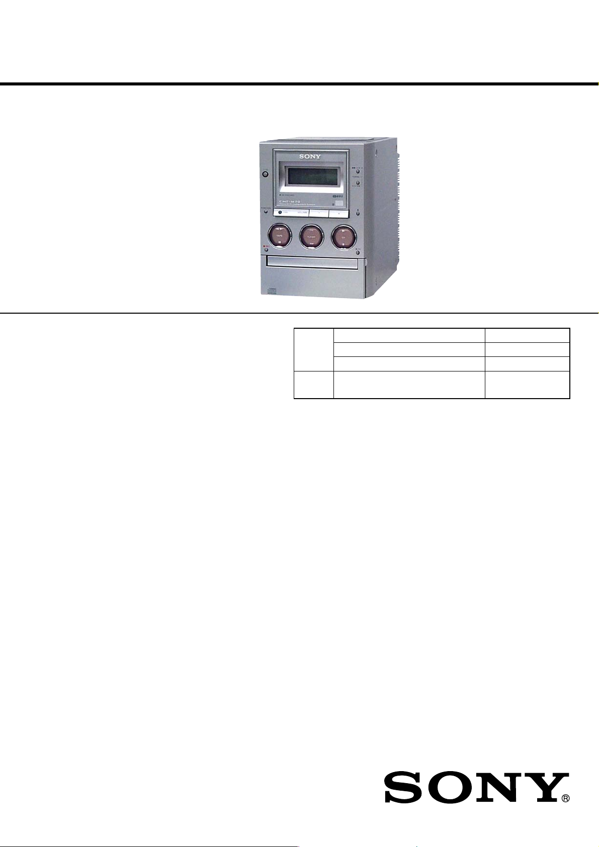
Sony HCDM-70 Service manual
Tape player section
Recording system 4-track 2-channel stereo
Frequency response 50 - 13,000 Hz (±3 dB),
using a Sony TYPE I
cassette
Tuner section
FM stereo, FM/AM superheterodyne tuner
FM tuner section
Tuning range
North American model: 87.5 - 108.0 MHz
(100-kHz step)
Other models: 87.5 - 108.0 MHz
(50-kHz step)
Antenna FM wire antenna
Antenna terminals 75 ohms unbalanced
Intermediate frequency 10.7 MHz
AM tuner section
Tuning range
Pan-American model: 530 - 1,710 kHz
(with the tuning interval
set at 10 kHz)
531 - 1,710 kHz
(with the tuning interval
set at 9 kHz)
European model: 531 - 1,602 kHz
(with the tuning interval
set at 9 kHz)
Amplifier section
For the U.S. model
AUDIO POWER SPECIFICATIONS
POWER OUTPUT AND TOTAL
HARMONIC DISTORTION:
With 6-ohm loads, both channels driven, from
70 - 20,000 Hz; rated 18 watts per channel
minimum RMS power, with no more than 0.9%
total harmonic distortion from 250 milliwatts to
rated output.
North American model:
Continuous RMS power output (reference):
20 + 20 W
(6 ohms at 1 kHz, 10%
THD)
Total harmonic distortion less than 0.07% (6 ohms at
1 kHz, 12 W)
European model:
DIN power output (rated): 15 + 15 W
(6 ohms at 1 kHz, DIN)
Continuous RMS power output (reference):
20 + 20 W
(6 ohms at 1 kHz, 10%
THD)
Music power output (reference):
40 + 40 W
DIN power output (rated): 15 + 15 W
(6 ohms at 1 kHz, DIN)
Continuous RMS power output (reference):
18 + 18 W
(6 ohms at 1 kHz, 10%
THD)
The following measured at 220 V AC, 60 Hz
DIN power output (rated): 12 + 12 W
(6 ohms at 1 kHz, DIN)
Continuous RMS power output (reference):
15 + 15 W
(6 ohms at 1 kHz, 10%
THD)
Inputs
AUDIO IN MD (VIDEO) (phono jacks):
Sensitivity 500/250 mV,
impedance 47 kilohms
Outputs
OPTICAL DIGITAL OUT (CD):
Optical
PHONES: Accepts headphones with
an impedance of 8 ohms
or more
SPEAKER: 6 ohms
Other models:
The following measured at 230 V AC, 60 Hz
CD player section
System Compact disc and digital
audio system
Laser Semiconductor laser
(λ = 780 nm)
Emission
duration: continuous
Wavelength 780 - 790 nm
Frequency response 2 Hz - 20 kHz (±0.5 dB)
HCD-M70
SERVICE MANUAL
Ver. 1.3 2005.03
HCD-M70 is the Amplifier, CD player, Tape
Deck and Tuner section in CMT-M70/M70K.
CD
Section
TAPE
Section
US Model
Canadian Model
AEP Model
UK Model
E Model
Austr alian Model
Model Name Using Similar Mechanism HCD-CP100
CD Mechanism Type CDM55F-K6BD41A
Optical Pick-up Name KSS-213DCP
Model Name Using Similar Mechanism NEW
9-873-633-04 Sony Corporation
2005C05-1 Personal Audio Group
© 2005.03 Published by Sony Engineering Corporation
SPECIFICATIONS
MICRO Hi-Fi COMPONENT SYSTEM
– Continued on next page –
HCD-M70
r
Other models: 530 - 1,710 kHz
Antenna AM loop antenna, external
Intermediate frequency 450 kHz
General
Power requirements
North American model: 120 V AC, 60 Hz
European model: 230 V AC, 50/60 Hz
Mexican model: 120 V AC, 60 Hz
Australian model: 230 V AC, 50/60 Hz
Thailand model: 220 V AC, 50/60 Hz
Other models: 110 - 120 V or 220 -
Power consumption
European model: See the nameplate
Other models: See the nameplate
Dimensions (w/h/d) Approx. 159 × 217 ×
Mass Approx. 4.5 kg
Design and specifications are subject to change
without notice.
(with the tuning interval
set at 10 kHz)
531 - 1,602 kHz
(with the tuning interval
set at 9 kHz)
antenna terminal
240 V AC, 50/60 Hz
Adjustable with voltage
selector
0.5 W (in the standby
mode)
315 mm incl. projecting
parts and controls
SAFETY CHECK-OUT
After correcting the original service problem, perform the following safety check before releasing the set to the customer:
Check the antenna terminals, metal trim, “metallized” knobs,
screws, and all other exposed metal parts for AC leakage.
Check leakage as described below.
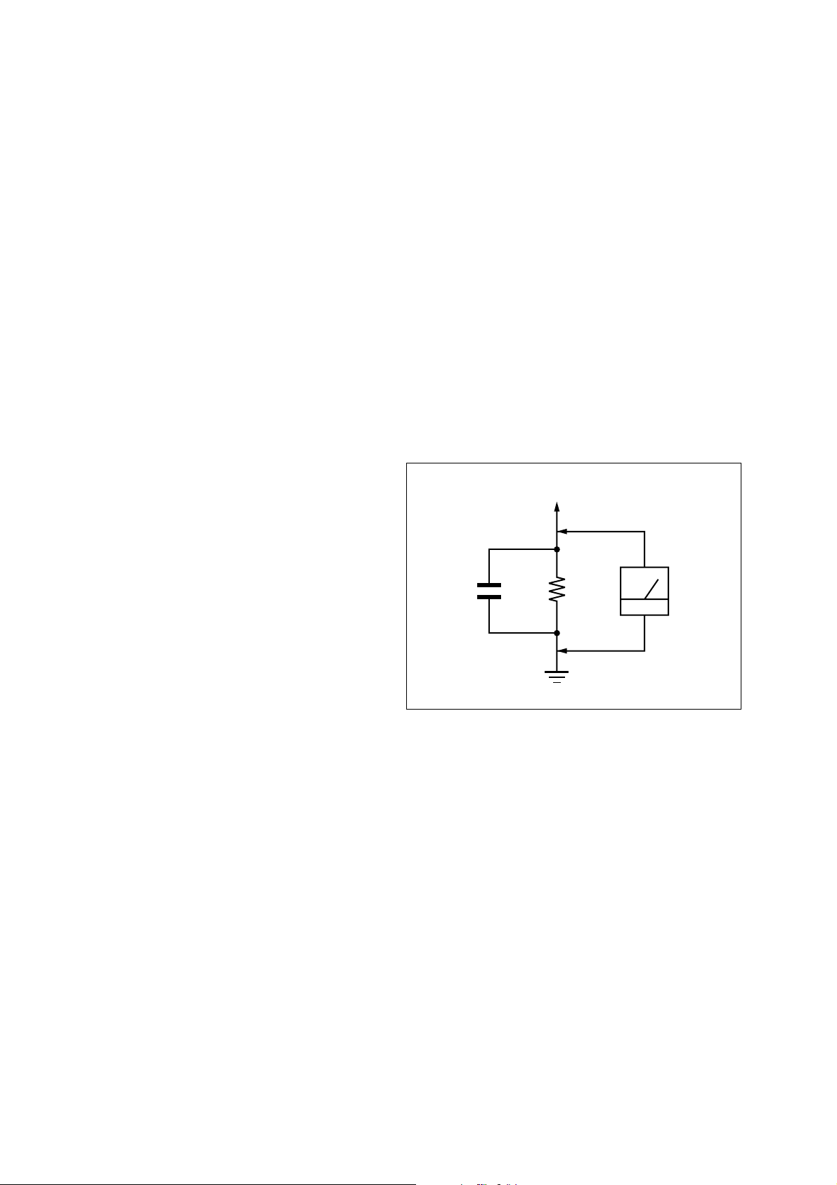
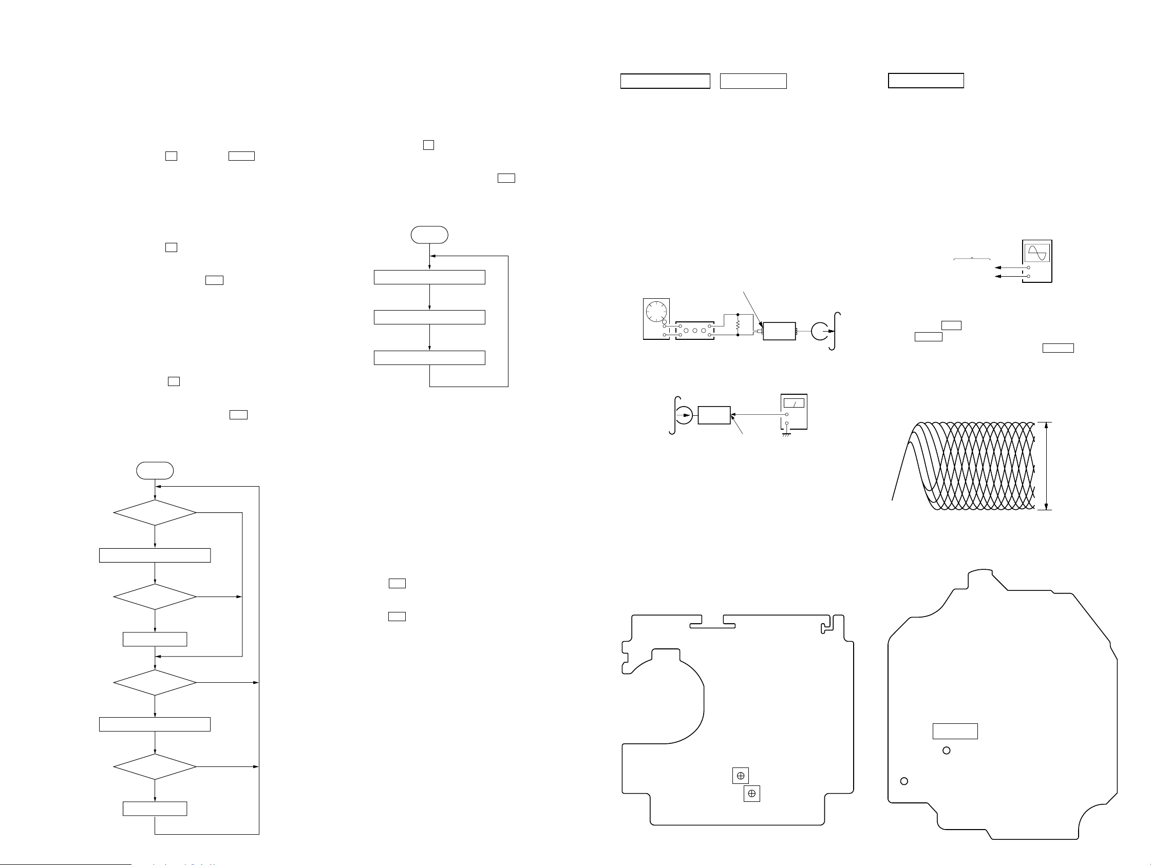
LEAKAGE TEST
The AC leaka ge from any exposed metal part to earth ground and
from all exposed metal parts to any exposed metal part having a
return to chassis, must not exceed 0.5 mA (500 microamperes.).
Leakage current can be measured by any one of three methods.
1. A commercial leakage tester, such as the Simpson 229 or RCA
WT -540A. Follo w the manufacturers’ instructions to use these
instruments.
2. A battery-operated A C milliammeter. The Data Precision 245
digital multimeter is suitable for this job.
3. Measuring the voltage drop across a resistor by means of a V OM
or battery-operated A C voltmeter . The “limit” indication is 0.75
V, so analog meters must have an accurate low-voltage scale.
The Simpson 250 and Sanwa SH-63Trd are examples of a passive VOM that is suitable. Nearly all battery operated digital
multimeters that have a 2 V A C range are suitable. (See Fig. A)
To Exposed Metal
Parts on Set
AC
0.15 µF
1.5 k
Ω
voltmete
(0.75 V)
Earth Ground
Fig. A. Using an AC voltmeter to check AC leakage.
SAFETY-RELATED COMPONENT WARNING!!
COMPONENTS IDENTIFIED BY MARK 0 OR DOTTED
LINE WITH MARK 0 ON THE SCHEMATIC DIAGRAMS
AND IN THE PARTS LIST ARE CRITICAL TO SAFE
OPERATION. REPLACE THESE COMPONENTS WITH
SONY PARTS WHOSE PART NUMBERS APPEAR AS
SHOWN IN THIS MANUAL OR IN SUPPLEMENTS PUBLISHED BY SONY.
2
ATTENTION AU COMPOSANT AYANT RAPPORT
À LA SÉCURITÉ!
LES COMPOSANTS IDENTIFIÉS P AR UNE MARQUE 0
SUR LES DIAGRAMMES SCHÉMATIQUES ET LA LISTE
DES PIÈCES SONT CRITIQUES POUR LA SÉCURITÉ
DE FONCTIONNEMENT. NE REMPLACER CES COMPOSANTS QUE PAR DES PIÈCES SONY DONT LES
NUMÉROS SONT DONNÉS DANS CE MANUEL OU
DANS LES SUPPLÉMENTS PUBLIÉS PAR SONY.
HCD-M70
CAUTION
Use of controls or adjustments or performance of procedures
other than those specified herein may result in hazardous radiation exposure.
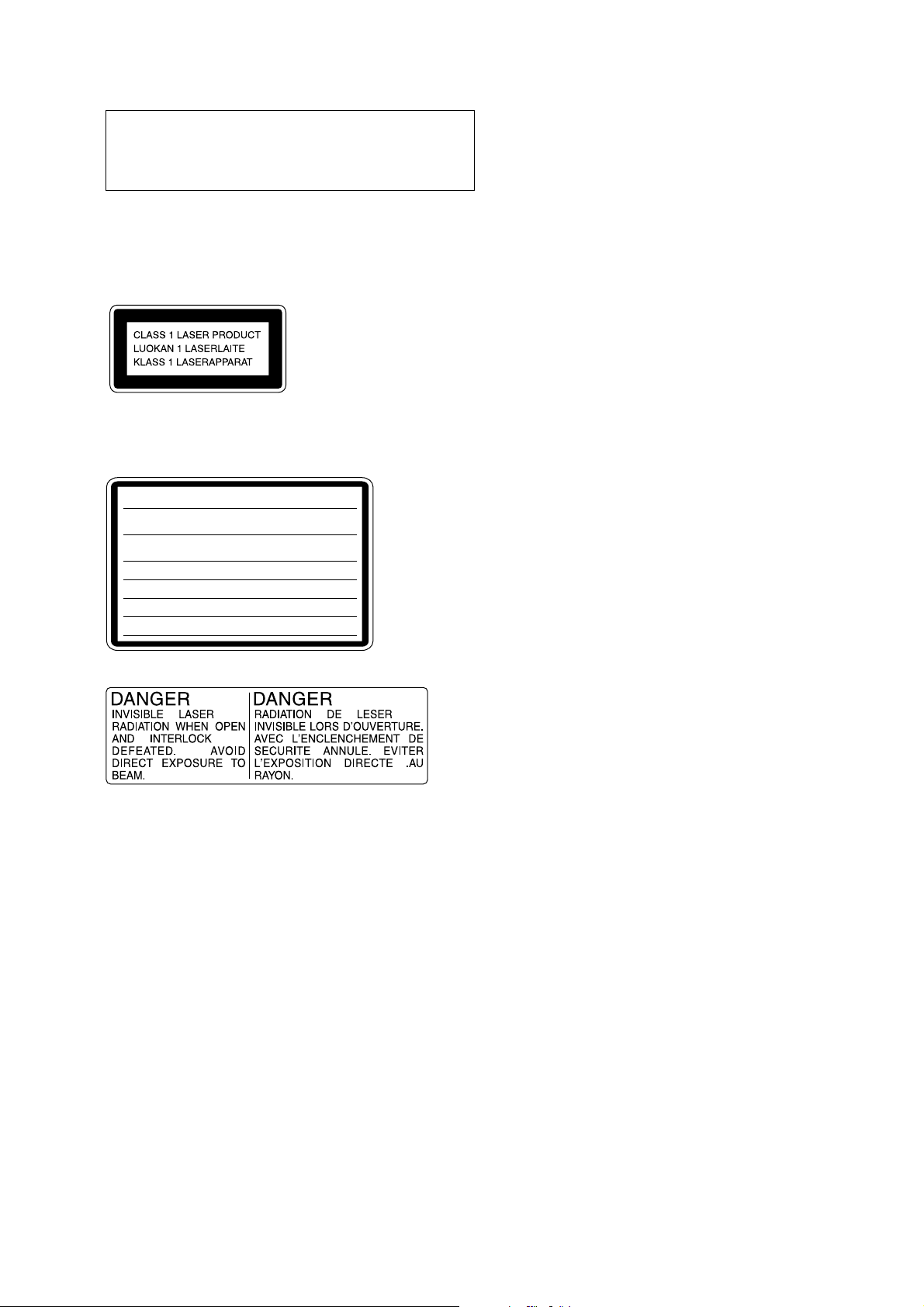
This appliance is classified as a CLASS 1 LASER product.
The CLASS 1 LASER PRODUCT MARKING is located on
the rear exterior.
Laser component in this product is capable of emitting radiation
exceeding the limit for Class 1.
The following caution label is located inside the unit.
CAUTION :
INTERLOCKS DEFEATED. AVOID EXPOSURE TO BEAM.
ADVARSEL :
SIKKERHEDSAFBRYDERE ER UDE AF FUNKTION. UNDGÅ UDSAETTELSE
FOR STRÅLING.
VORSICHT :
ABDECKUNG GEÖFFNET UND SICHEREITSVERRIEGELUNG
ÜBERBRÜCKT. NICHT DEM STRAHL AUSSETZEN.
VARO! :
TIINA NÄKYMÄTTÖMÄLLE LASERSÄTEILYLLE. ÄLÄ KATSO SÄTEESEEN.
VARNING :
OCH SPÄRREN ÄR URKOPPLAD. BETRAKTA EJ STRÅLEN.
ADVERSEL :
SIKKERHEDSLÅS BRYTES. UNNGÅ EKSPONERING FOR STRÅLEN.
VIGYAZAT! :
GÁRVESZÉLY! KERÜLJE A BESUGÁRZÁST!
INVISIBLE LASER RADIATION WHEN OPEN AND
USYNLIG LASERSTRÅLING VED ÅBNING NÅR
UNSICHTBARE LASERSTRAHLUNG, WENN
AVATTAESSA JA SUOJALUKITUS OHITETTAESSA OLET ALT-
OSYNLING LASERSTRÅLING NÄR DENNA DEL ÄR ÖPPNAD
USYNLIG LASERSTRÅLING NÅR DEKSEL ÅPNES OG
A BURKOLAT NYITÁSAKOR LÁTHATATLAN LÉZERSU-
Notes on chip component replacement
•Never reuse a disconnected chip component.
• Notice that the minus side of a tantalum capacitor may be damaged by heat.
Flexible Circuit Board Repairing
•Keep the temperature of the soldering iron around 270 ˚C during repairing.
• Do not touch the soldering iron on the same conductor of the
circuit board (within 3 times).
• Be careful not to apply force on the conductor when soldering
or unsoldering.
TABLE OF CONTENTS
1. SERVICING NOTES............................................... 4
2. GENERAL ................................................................... 5
3. DISASSEMBLY
3-1. Disassembl y Flow ........................................................... 6
3-2. Panel (Side) (L), Panel (Side) (R) .................................. 7
3-3. Top Panel Section............................................................ 7
3-4. Mechanical Deck (Tape) ................................................. 8
3-5. F ront Panel Section ......................................................... 8
3-6. Back Panel Assy .............................................................. 9
3-7. MAIN Board ................................................................... 9
3-8. CD Mechanism Deck (CDM55F-K6BD41A) ................ 10
3-9. Base Unit (BU-K6BD41A) ............................................. 11
3-10. Loading Board................................................................. 11
3-11. Cam (CDM55) ................................................................ 12
4. TEST MODE.............................................................. 13
5. ELECTRICAL ADJUSTMENTS
Deck Section ................................................................... 13
CD Section ...................................................................... 13
6. DIAGRAMS
6-1. Block Diagram – CD SERVO Section – ....................... 14
6-2. Block Diagram – TUNER/TAPE DECK Section – ...... 15
6-3. Block Diagram – MAIN Section – ................................ 16
6-4. Note for Printed Wiring Boards and
Schematic Diagrams ....................................................... 17
6-5. Printed Wiring Board – CD Board – ............................. 18
6-6. Schematic Diagram – CD Board – ................................ 19
6-7. Printed Wiring Board – TC Board –.............................. 20
6-8. Schematic Diagr am – TC Board –................................. 21
6-9. Schematic Diagram – MAIN Board (1/2) – .................. 22
6-10. Schematic Diagram – MAIN (2/2)/JACK Boards –...... 23
6-11. Printed Wiring Boards – MAIN/JACK Boards – .......... 24
6-12. Printed Wiring Boards
– CONTROL/LOADING/VIDEO Boards – .................. 26
6-13. Schematic Diagram – CONTROL/LOADING/
SWITCH (1/2)/VIDEO Boards – ................................... 27
6-14. Printed Wiring Board – SWITCH Board – ................... 28
6-15. Schematic Diagram – SWITCH Board (2/2) – ............. 29
6-16. Printed Wiring Board – POWER Board – ..................... 30
6-17. Schematic Diagram – POWER Board –........................ 31
6-18. IC Pin Function Description ........................................... 34
7. EXPLODED VIEWS
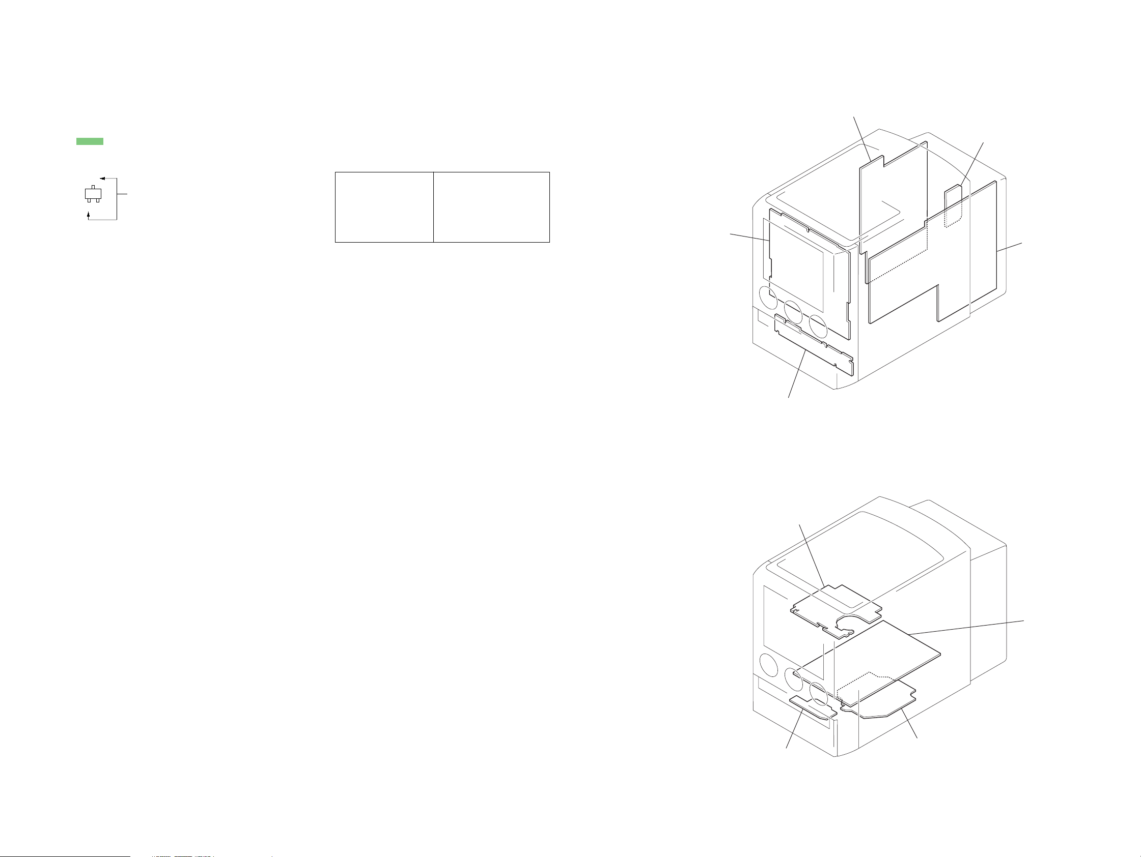
7-1. Panel (Side) Section ........................................................ 36
7-2. F ront Panel Section ......................................................... 37
7-3. Top Panel Section............................................................ 38
7-4. Chassis Section-1 ............................................................ 39
7-5. Chassis Section-2 ............................................................ 40
7-6. CD Mechanism Deck (CDM55F-K6BD41A) ................ 41
7-7. Base Unit (BU-K6BD41A) ............................................. 42
8. ELECTRICAL PARTS LIST ............................... 43
3
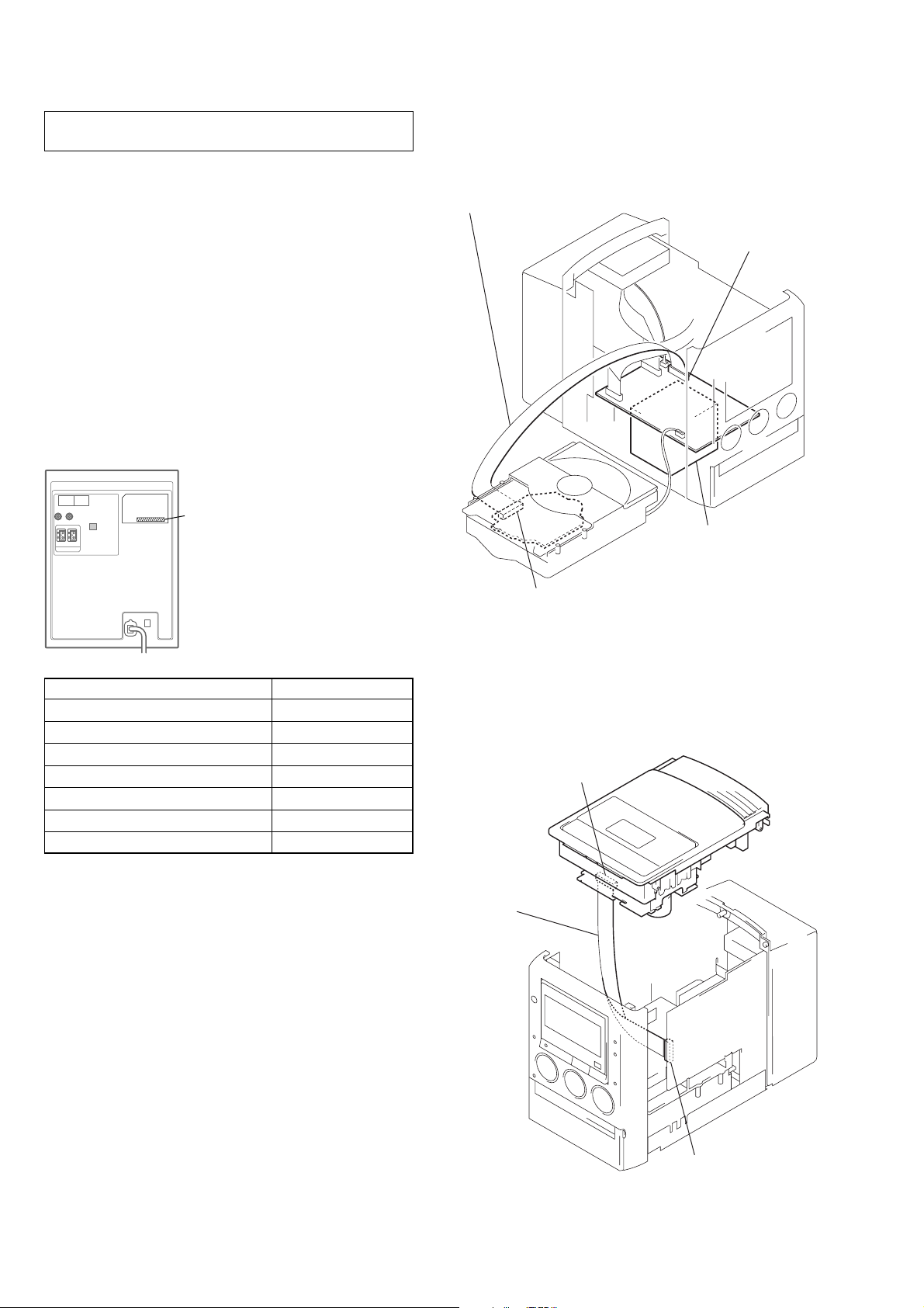
HCD-M70
TC board (CN301)
main board (CN301)
Connect jig (extension cable J-2501-167-A)
to the main board (CN301) and TC board (CN301).
SECTION 1
SERVICING NOTES
NOTES ON HANDLING THE OPTICAL PICK-UP
BLOCK OR BASE UNIT
The laser diode in the optical pick-up block may suffer electrostatic break-down because of the potential difference generated
by the charged electrostatic load, etc. on clothing and the human
body.
During repair, pay attention to electrostatic break-down and also
use the procedure in the printed matter which is included in the
repair parts.
The flexible board is easily damaged and should be handled with
care.
NOTES ON LASER DIODE EMISSION CHECK
The laser beam on this model is concentrated so as to be focused
on the disc reflective surface by the objective lens in the optical
pick-up block. Therefore, when checking the laser diode emission, observe from more than 30 cm away from the objectiv e lens.
MODEL IDENTIFICATION
– Rear Panel –
Part No.
SERVICE POSITION
In checking the CD block, prepare jig (extension cable J-2501011-B: 1.25 mm Pitch, 19 cores, Length 300 mm).
Connect jig (extension cable J-2501-011-B)
to the control board (CN805) and CD board (CN101).
control board (CN805)
Any box to put.
Model Name Part No.
AEP and UK models 4-238-716-0
US and Canadian models 4-238-888-0
Singapore model 4-238-889-0
Mexican model 4-239-812-0
Australian model 4-240-890-0
Korean model 4-240-891-0
Thai model 4-240-892-0
CD board (CN101)
[]
[]
[]
[]
[]
[]
[]
In checking the tape deck section, prepare jig (extension cable J2501-167-A: 1.25 mm Pitch, 17 cores, Length 300 mm).
4
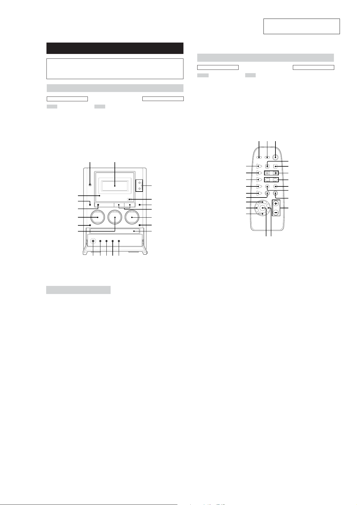
List of Button Locations and Reference Pages
How to use this page
Use this page to find the location of buttons and other
parts of the system that are mentioned in the text.
Main unit
ALPHABETICAL ORDER
A – F
CD disc tray 9 (8)
CD SYNCHRO qa (13, 14)
CD SYNCHRO indicator w; (14)
CD N 7 (8, 9)
CD X 7 (8)
DIRECTION q; (12–14)
Display window 2
DSG qk (15, 18)
FUNCTION ql (8–14, 18)
P – V
PHONES jack qf
PLAY MODE/TUNING MODE
qd (8–11, 14)
Remote sensor 4
REPEAT/FM MODE qs (8, 11)
TAPE nN qj (12–14)
TAPE X qj (12–14)
TUNER AM qg (9–11)
TUNER FM qg (9–11)
TUNING +/– 3 (9–11)
VOLUME +/– 6 (17)
SECTION 2
GENERAL
Illustration number
PLAY MODE qg (9, 13, 14)
Name of button/part Reference page
r
RR
BUTTON DESCRIPTIONS
@/1 (power) 1 (7, 10, 15, 17)
m/M 3 (8, 12)
l/L 3 (8, 9, 14)
x 5 (8, 12, 13)
Z CD 8 (8)
z REC qh (13)
Remote Control
ALPHABETICAL ORDER
A – M
CD REPEAT qk (8)
CD N ws (8, 9)
DIR MODE ql (12–14)
DISPLAY 2 (11, 16)
DSG 1 (15)
ENTER qd (7, 10, 14, 15, 17)
FM MODE 9 (11)
FUNCTION qj (8–14, 18)
MEMORY qh (10)
This section is extracted from
instruction manual.
S – V
SLEEP qf (16)
TAPE nN w; (12–14)
TIMER SELECT qs (15, 17)
TIMER SET qg (7, 14, 17)
TUNER/BAND wa (9–11)
TUNING MODE/PLAY MODE
q; (8–11, 14)
VOL +/– qa (17)
123
HCD-M70
BUTTON DESCRIPTIONS
X 4 (8, 12, 14)
x 5 (8, 9, 12–14)
./> 6 (7–10, 14, 15, 17)
m/M 7 (8–12)
@/1 (power) 3 (7, 15, 17)
z REC 8 (13)
w;
ql
qk
qj
qh
qg
GB
4
Setting the clock
1
Turn on the system.
2
Press TIMER SET on the remote.
3
Press ./> on the remote
repeatedly to set the hour.
4
Press ENTER on the remote.
The minute indication flashes.
5
Press ./> on the remote
repeatedly to set the minute.
6
Press ENTER on the remote.
The clock will begin operating.
To adjust the clock
1
Press TIMER SET on the remote.
2
Press . or > on the remote to select
“SET CLOCK”, then press ENTER on the
remote.
3
Do the same procedures as step 3 to 6
above.
1
?/1
nN N
z
2
ws
wa
ML
3
lm
4
x
5
6
XX
7
Z
8
w;
ql
qk
qj
qh
qg
qf
5
6
7
8
9
0
qa
9
qsqd
0qaqsqdqf
GB
5
4
5
HCD-M70
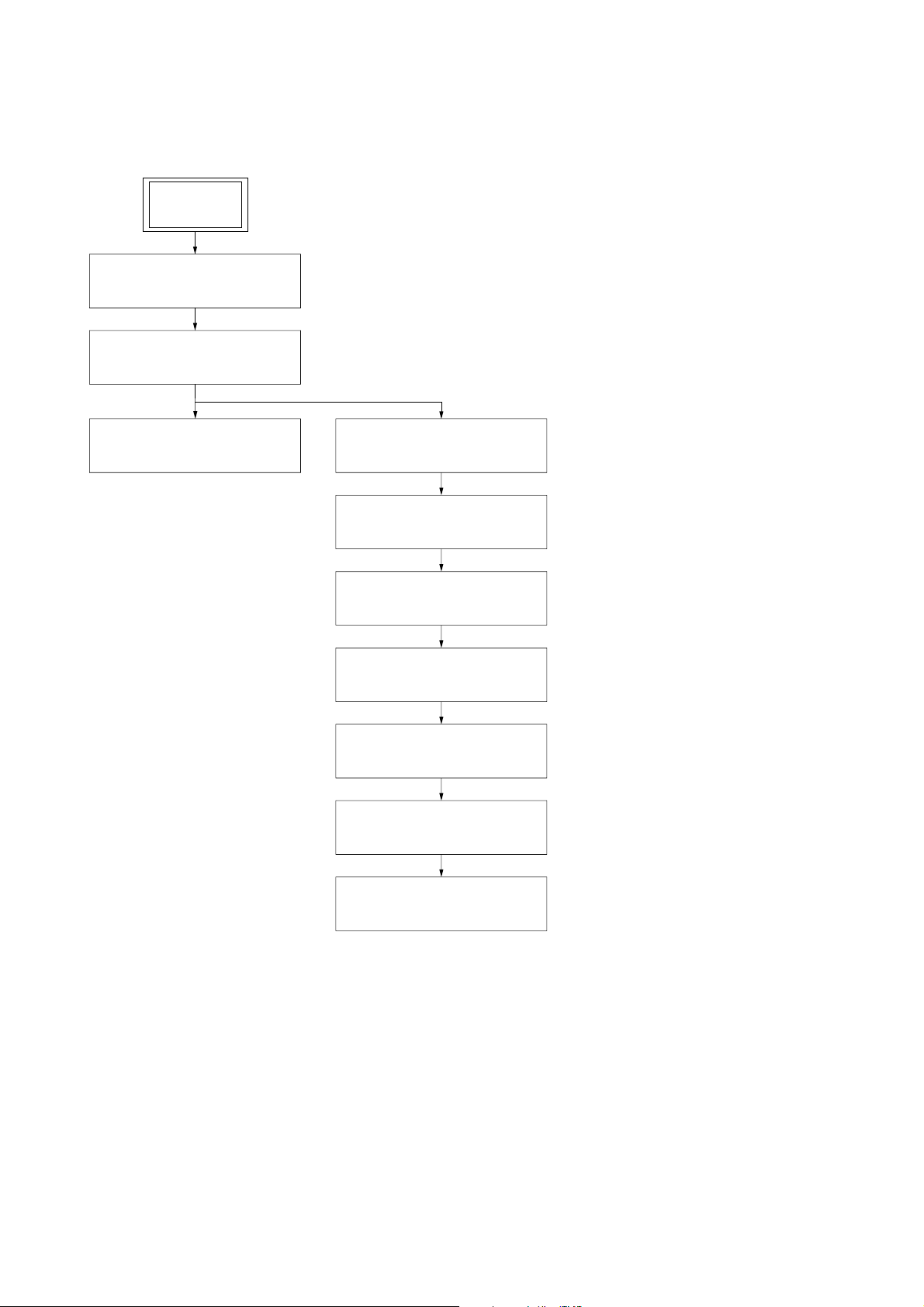
• This set can be disassembled in the order shown below.
3-1. DISASSEMBLY FLOW
SET
3-2. PANEL (SIDE) (L),
PANEL (SIDE) (R)
(page 7)
3-3. TOP PANEL SECTION
(page 7)
SECTION 3
DISASSEMBLY
3-4. MECHANICAL DECK (TAPE)
(page 8)
3-5. FRONT PANEL SECTION
(page 8)
3-6. BACK PANEL ASSY
(page 9)
3-7. MAIN BOARD
(page 9)
3-8. CD MECHANISM DECK
(CDM55F-K6BD41A)
(page 10)
3-9. BASE UNIT (BU-K6BD41A)
(page 11)
3-10.LOADING BOARD
(page 11)
3-11.CAM (CDM55)
(page 12)
6
Note: Follow the disassembly procedure in the numerical order given.
1
four screws
(BTP3
×
10)
2
3
panel (side) (L)
1
screw
(BTP3
×
10)
4
screw
(BTP3
×
10)
4
four screws
(BTP3
×
10)
5
6
panel (side) (R)
)
3-2. PANEL (SIDE) (L), PANEL (SIDE) (R)
HCD-M70
3-3. TOP PANEL SECTION
3
wire (flat type) (17 core)
(CN301)
4
top panel section
1
screw
(BTP3 × 10
2
7
HCD-M70
)
3-4. MECHANICAL DECK (TAPE)
qd
mechanical deck
(tape)
9
0
MD bracket (L)
two screws
(BVTT2.6
×
5)
2
3
shield case (TC)
5
connector
1
two screws
(BVTP3
4
FFC cable 8P
×
6
two screws
(BVTT2.6
8)
3-5. FRONT PANEL SECTION
1
FFC cable 18P (CN802)
1
FFC cable 20P (CN803)
1
two screws
(BVTP3
qa
two screws
(BVTT2.6
×
5)
8
TC board
7
6
screw
(BVTT2.6
×
5)
×
8)
qs
MD bracket (R
×
5)
1
FFC cable 15P (CN801)
2
4
front panel section
3
three screws
(BTP3 × 10)
connector
(CN304)
8
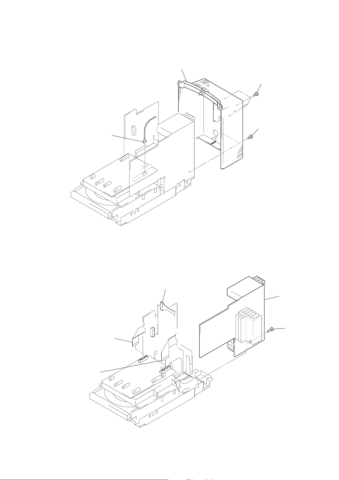
3-6. BACK PANEL ASSY
1
connector
(CN809)
3
back panel assy
2
four screws
(BTP3
2
two screws
(BTP3
×
10)
×
10)
HCD-M70
3-7. MAIN BOARD
1
FFC cable 17P (CN804)
1
FFC cable 21P (CN806)
2
connector
(CN101)
4
main board
3
screw
(BTP3 × 12)
9
HCD-M70
k
)
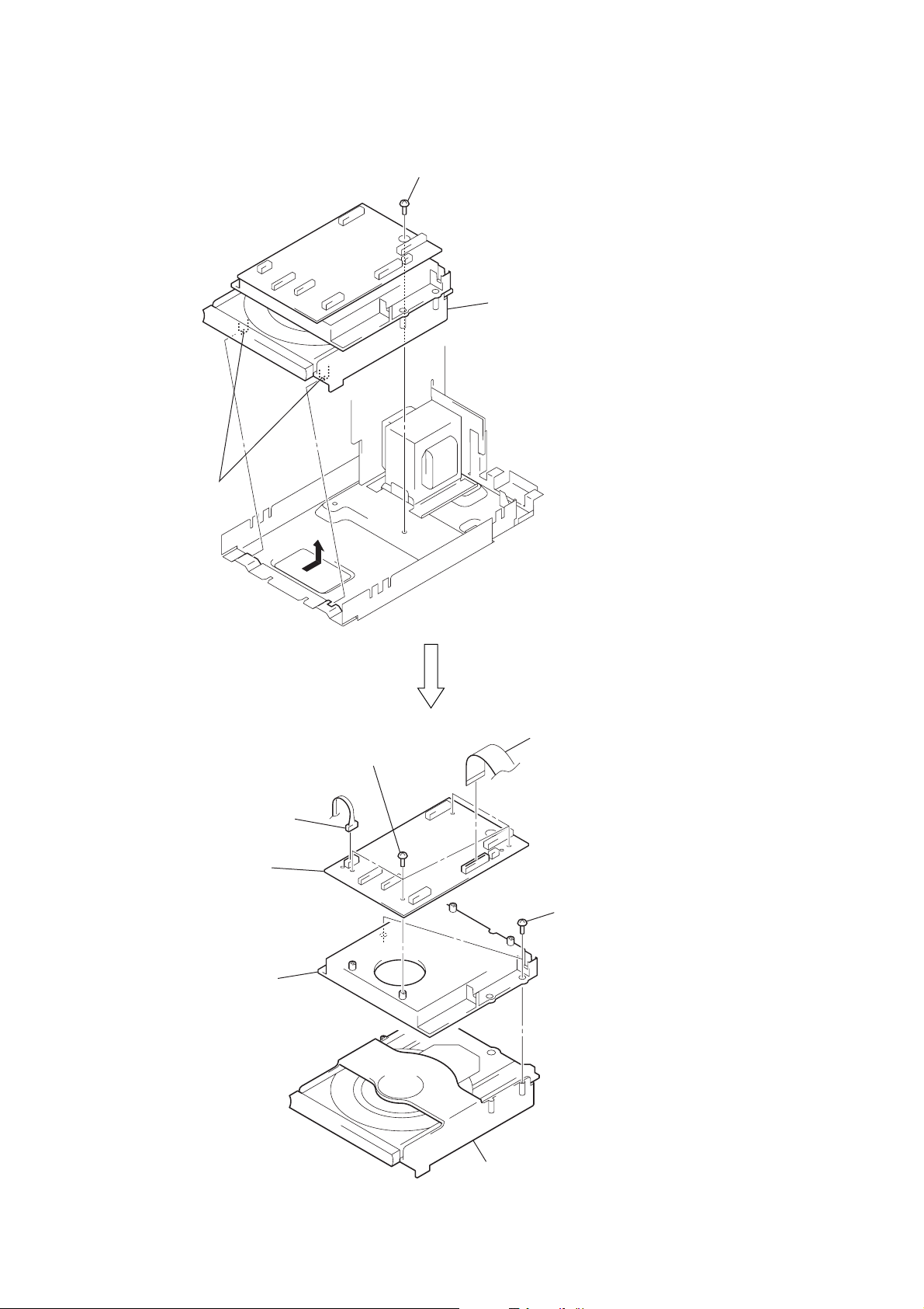
3-8. CD MECHANISM DECK (CDM55F-K6BD41A)
1
screw
(BVTP3
×
8)
3
Remove the CD mechanism dec
in the direction of the arrow.
2
two claws
7
control board
5
connector
(CN807)
6
four screws
(DIA. 2.6 × 8)
4
flexible flat cable (19 core
(CN805)
8
two screws
(BTP3
×
8)
10
9
bracket (MPEG)
0
CD mechanism deck
(CDM55F-K6BD41A)
3-9. BASE UNIT (BU-K6BD41A)
2
belt (CDM55)
B
3
Pull the tray pushing B.
4
two screws
(BTP2.6
×
6)
5
loading board
1
Rotate the gear(B) in
the direction of arrow
A
.
A
2
base unit
(BU-K6BD41A)
1
floating screw
(PTPWHM2.6)
HCD-M70
3-10. LOADING BOARD
11
HCD-M70
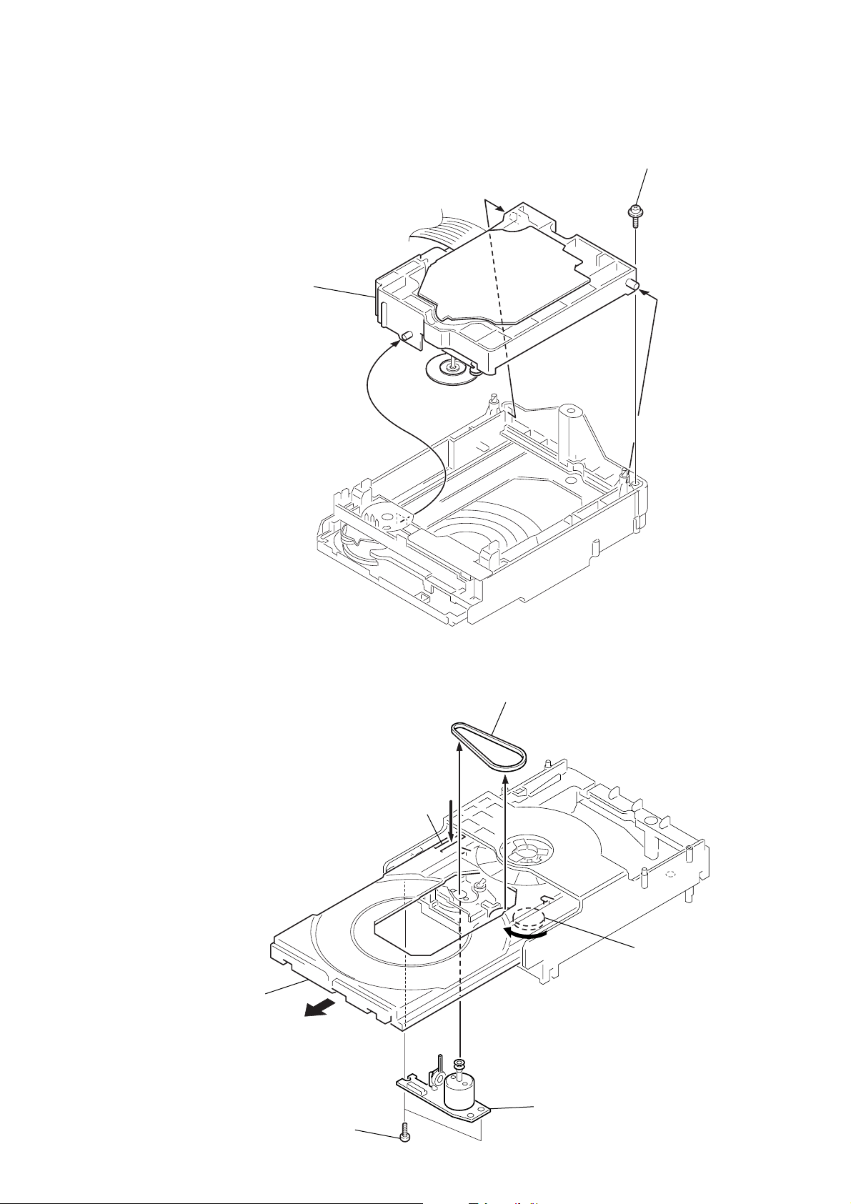
3-11. CAM (CDM55)
3 spacer (55)
4 pulley (LDG)
2 lever (SW)
1 torsion spring
6 gear (B)
5 gear (A)
7 roller
8 cam (CDM55)
12
V
attenuator
set
MAIN board
AUDIO IN (MD/VIDEO) jack (SJ302)
L-CH, R-CH
1) 315 Hz
2) 10 kHz
50 mV (– 23.8 dB)
600
Ω
blank tape
CN-123
AF OSC
+
–
set
recorded
portion
MAIN board
SPEAKER terminals (SJ301)
L-CH, R-CH
level meter
RV101 (L)
RV201 (R)
REC Bias
Adjustment
– TC BOARD (Component Side) –
SECTION 4
TEST MODE
HCD-M70
SECTION 5
ELECTRICAL ADJUSTMENTS
[COLD RESET]
• The cold reset clears all data including preset data stored in the
RAM to initial conditions. Execute this mode when returning
the set to the customer.
Procedure:
1. Turn ON the power.
2. Press three buttons of x , [DSG], and CD X simultaneously.
3. The set is reset.
[LIQUID CRYSTAL DISPLAY ALL LIT CHECK
MODE]
Procedure:
1. Set to standby state.
2. Press three buttons of x , [DSG], and
[PLAY MODE/TUNING MODE] simultaneously.
3. Liquid crystal display are all turned on.
4. To exit from this mode, press the I/1 button to turn the power
OFF.
[TAPE DECK AGING MODE]
This mode can be used for operation check of tape deck section.
Procedure:
1. Set a tape in the tape deck.
2. Set to standby state.
3. Press three buttons of x , [DSG], and [CD SYNCHRO] si-
multaneously.
4. The aging is executed in bellow sequence.
5. To exit from the aging mode, press the I/1 button to turn the
power OFF.
Aging mode sequence:
FWD Play
REC pause for 3 seconds
FWD REC
Fast forward
REV Play
Start
1 minute
3 minutes
Shut off
Shut off
Shut off
[CD AGING MODE]
This mode can be used for operation check of CD section.
Procedure:
1. Load a CD disc.
2. Set to standby state.
3. Press three buttons of x , [DSG], and [REPEAT/FM MODE] simul-
taneously.
4. The aging is executed in bellow sequence.
5. To exit from the aging mode, press the I/1 button to turn the
power OFF.
Aging mode sequence:
Start
Open the disc tray
Close the disc tray
Play the last track
[CHANGE-OVER MD/VIDEO]
Procedure:
1. Set to standby state.
2. Press the [DSG] and the [FUNCTION] buttons simultaneously.
3. The function change over to MD or VIDEO by turns.
[CHANGE-OVER THE AM TUNING INTERVAL]
(Except AEP and UK models)
•The AM tuning interval can be changed over 9 kHz or 10 kHz.
Procedure:
1. Press the I/1 button to turn the power ON.
2. Select the function “TUNER”, and press the [TUNER AM]
button to select the “AM”.
3. Press the I/1 button to turn the power OFF.
4. Change over to 9 kHz:
Press the [TUNING --] and the [TUNER AM] buttons simulta-
neously.
Change over to 10 kHz:
Press the [TUNING +] and the [TUNER AM] buttons simultaneously.
DECK SECTION
Note: Confirm each contents of this section first of all. If the results are
not satisfied, do the adjustment.
0 dB=0.775 V
1. The adjustments should be performed with the rated power supply voltage unless otherwise noted.
2. The adjustments should be performed in the order given in this
service manual.
3. The adjustments should be performed for both L-CH and RCH.
REC Bias Adjustment
Procedure:
1. Mode: REC
FUNCTION: VIDEO
2. Mode: Playback
3. Confirm playback the signal recorded in step 1 become speci-
fied values as follows.
If these values are out of specification values, adjust the RV101
(L-CH) and RV201 (R-CH) on the TC board to repeat steps
1and 2.
Specified values:Playback output of 315 Hz to playback
output of 10 kHz: ± 0.5 dB
Adjustment Location: TC board
CD SECTION
Note:
1. CD Block is basically constructed to operate without adjustment.
2. Use YEDS-18 disc (3-702-101-01) unless otherwise indicated.
3. Use an oscilloscope with more than 10 MΩ impedance.
4. Clean the object lens by an applicator with neutral detergent
when the signal level is low than specified value with the following checks.
5. Check the focus bias check when optical block is replaced.
Focus Bias Check
BD board
TP (RF)
TP (VC)
Procedure :
1. Connect oscilloscope to TP (RF) and TP (VC) on the CD board.
2. Press the I/1 button to turn the power on, and press
the Z CD button to open the CD disc tray.
3. Put disc (YEDS-18) in and press the CD N button to play-
back.
4. Confirm that oscilloscope waveform is as shown in the figure
below. (eye pattern)
A good eye pattern means that the diamond shape ( ) in the
center of the waveform can be clearly distinguished.
Checking Location:
– CD BOARD (Conductor Side) –
oscilloscope
(DC range)
+
–
level:
1.1
s
VOLT/DIV: 200 m
TIME/DIV: 500 ns
±
0.2 Vp-p
REC pause for 3 seconds
REV REC
Rewind
1 minute
3 minutes
Shut off
IC103
TP (RF)
TP (VC)
1313
HCD-M70
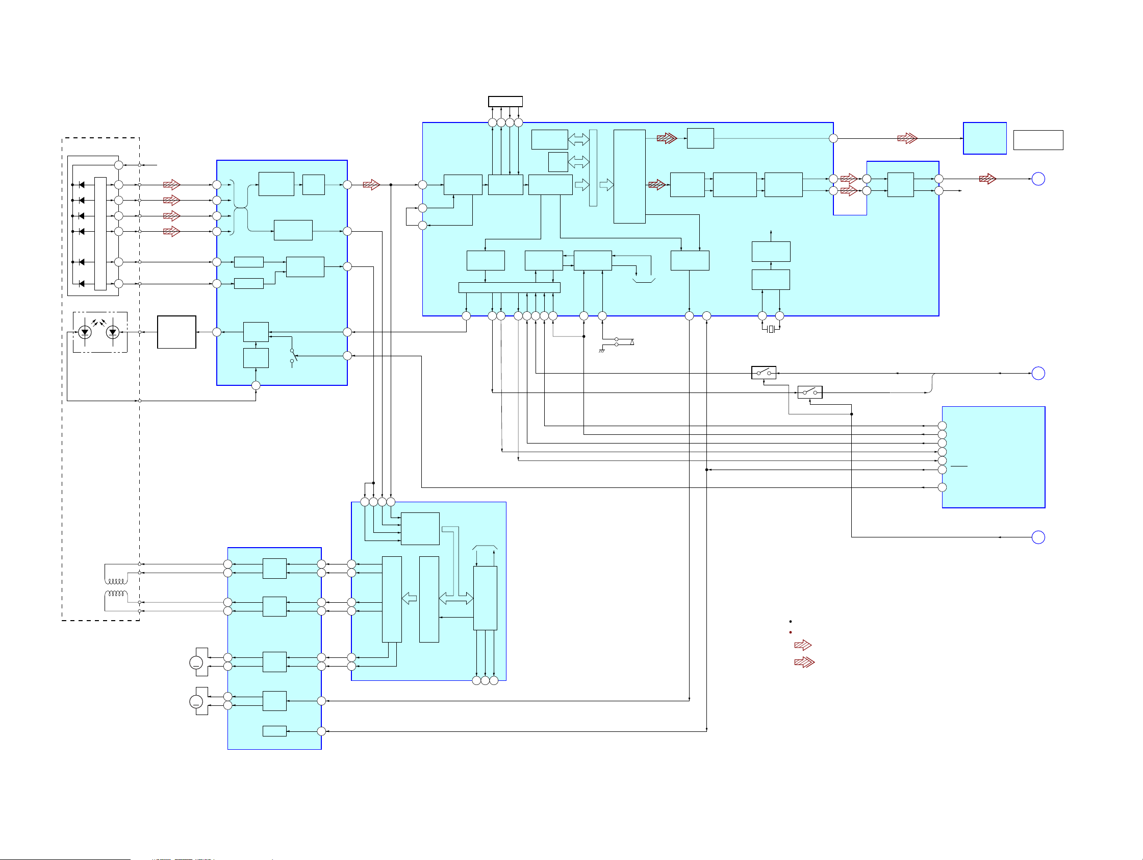
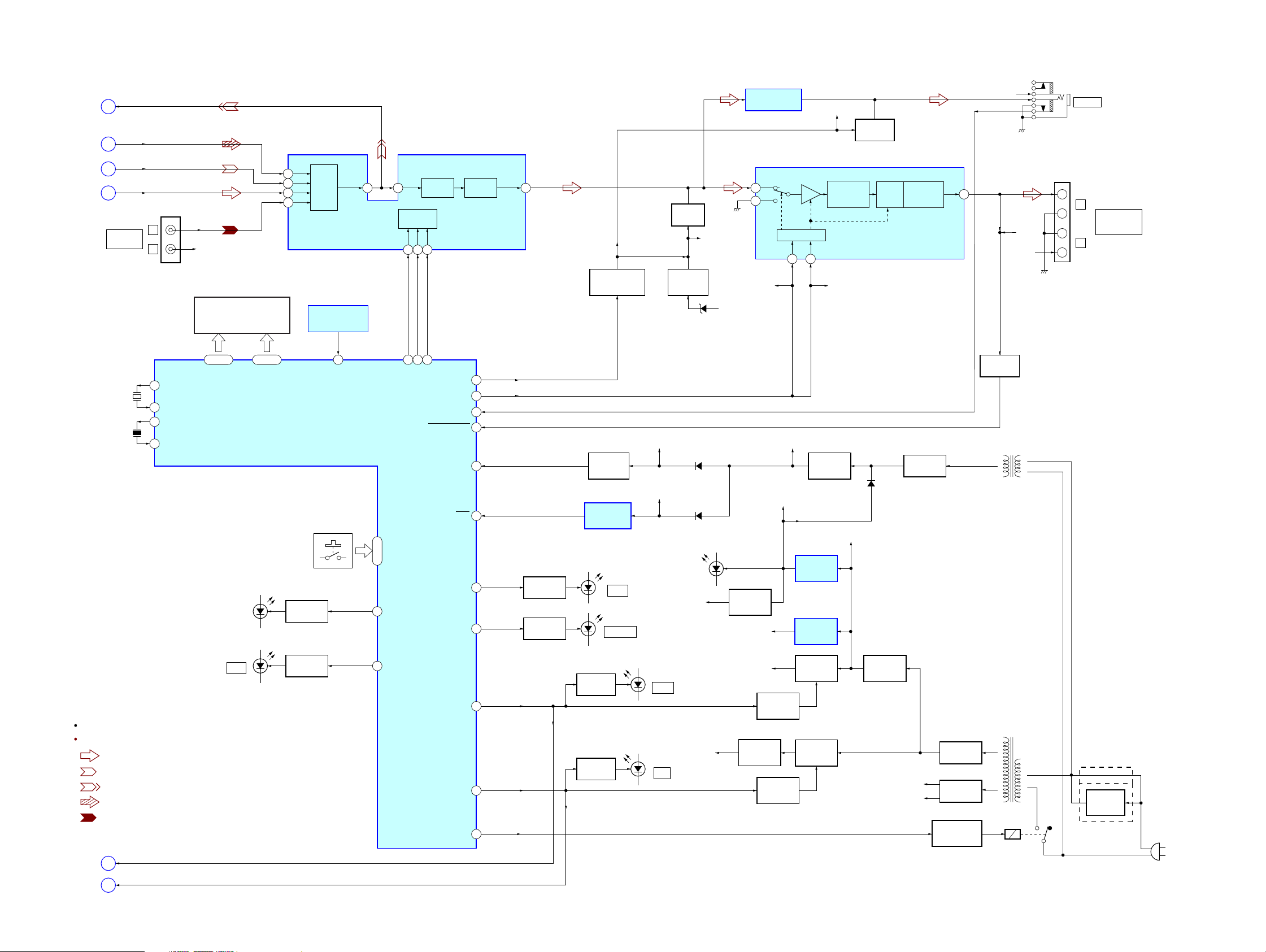
6-1. BLOCK DIAGRAM – CD SERVO Section –
SECTION 6
DIAGRAMS
PICK-UP BLOCK
(KSS-213DCP)
DETECTOR
LASER DIODE
OPTICAL
I-V AMP
VCC
7 D+5V
4
2
1
5
10
6
LD
LDPD
PD
AUTOMATIC
POWER
CONTROL
Q101
FOCUS/TRACKING ERROR AMP
A
5
B
6
C
7
D
8
F
10
FI-V AMP
E
11
EI-V AMP
LD
3
APC LD
AMP
APC PD
AMP
PD
4
RF AMP
IC103
RF
SUMMING
AMP
ERROR AMP
FOCUS
TRACKING
ERROR AMP
RF EQ
AMP
RFO
LD ON
HOLD SW
FILTER
54 56 53 55
ERROR
FILI
PCO
FILO
CLTV
CORRECTOR
16k
RAM
RFAC
16
FE
14
TE
13
22
21
ASYMMETRY
51
CORRECTION
ASYI
49
ASYO
48
XLON
SUBCODE
PROCESSOR
CPU INTERFACE
SQSO
DIGITAL
PLL
SENS
DEMODULATOR
SERVO AUTO
SEQUENCER
XLAT
SCOR
CLOK
EFM
DATA
SQCK
2576208114
DIGITAL SIGNAL PROCESSOR,
DIGITAL FILTER, D/A CONVERTER
IC101 (1/2)
D/A
INTERFACE
INTERNAL BUS
SERVO
INTERFACE
MIRR/DFCT/FOK DETECTOR
SSTP
IC101 (2/2)
SCLK
9 27
TO
S101
(LIMIT)
DIGITAL
SERIAL
IN
INTERFACE
DIGITAL
CLV
MDP
26
OUT
NOISE SHAPER
XRST
3
DIGITAL
FILTER
INTEGRATOR
CLOCK
GENERATOR
TIMING
LOGIC
XTAL
X101
16.9344MHz
Q800
Q800, 801
CD ON SWITCH
PWM
&
XTAO
6766
Q801
D OUT
AOUT1
AOUT2
60
70
77
AIN1
515171
AIN2
76
BUFFER
CLK
SQSO
LOUT1
LOUT2
72
75
OPTICAL
TRANSCEIVER
IC321
R-CH
DIGITAL OUT (CD)
CD-L
CLK, SQSO
OPTICAL
A
B
(Page 16)
(Page 15)
2-AXIS DEVICE
(TRACKING)
(FOCUS)
M102
(SLED)
M101
(SPINDLE)
10
CD-DATA
11
C-SQCK
C-LATCH
19
C-SENSE
18
C-SCOR
100
C-RST
86
13
HOLD
41 39 4340
FE
TE
SE
RFDC
SPINDLE/SLED MOTOR DRIVE,
FOCUS/TRACKING COIL DRIVE
IC102
CH2OUTF
12
CH2OUTR
11
CH1OUTF
14
CH1OUTR
13
CH3OUTF
17
MM
MM
18
CH4OUTF
15
CH4OUTR
16
CH3OUTR
MOTOR
COIL
DRIVE
DRIVE
COIL
DRIVE
MOTOR
DRIVE
MOTOR
DRIVE
CH2 FIN
CH2RIN
CH1FIN
CH1RIN
CH3FIN
CH3RIN
CH4SIN
5
6
2
3
24
23
25
TRDR
31
TFDR
30
FRDR
33
FFDR
32
SFDR
28
SRDR
29
A/D
CONVERTER
PWM GENERATOR
FOCUS/TRACKING/SLED
SERVO DSP
FOCUS/TRACKING/SLED
TO
SERVO
INTERFACE
IC101 (1/2)
DETECTOR
MIRR/DFCT/FOK
DFCT
FOK
23 2224
MIRR
DIGITAL SERVO
PROCESSOR
IC101 (2/2)
R-CH : R-ch is omitted due to same as L-ch.
SIGNAL PATH
: CD PLAY (ANALOG)
: CD PLAY (DIGITAL OUT)
SYSTEM CONTROLLER
IC801 (1/3)
CD-ON
C
(Page 16)
MUTE
MUTE
20
1414
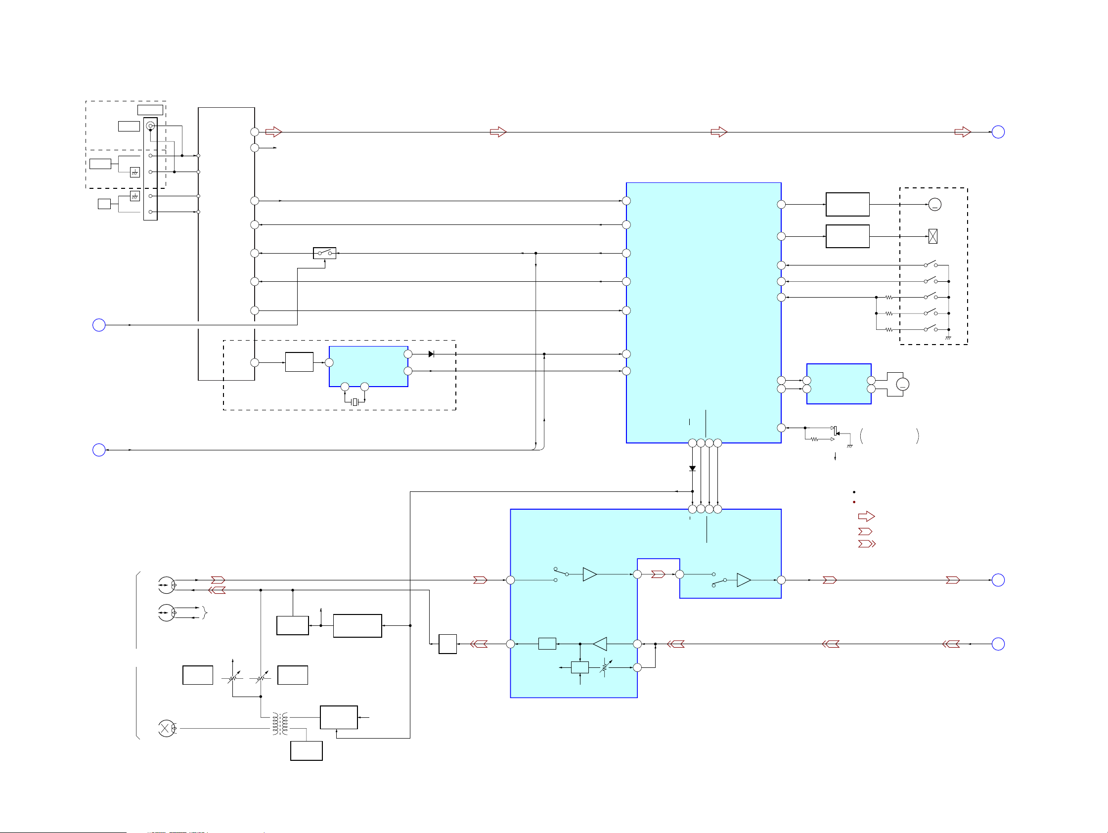
6-2. BLOCK DIAGRAM – TUNER/TAPE DECK Section –
TU1
TUNER UNIT
FM ANT
ANT GND
ANT GND
AM ANT
4
L-CH
3
R-CH R-CH
5
TUNED
9
DI
8
CK
10
CE
7
DO
TUNER ON SWITCH
Q804
(Page 16)
(AEP, UK)
FM75Ω
FM75Ω
(EXCEPT AEP, UK)
AM
TU-ON
D
ANENNA
17
TUNED
5
TU-DATA
8
C-CLK/TU-CLK
31
TU-CE
23
TU-COUNT
SYSTEM CONTROLLER
IC801 (2/3)
MOT-CON
SOL-CON
SENSOR
T-MODE
TC-SW
HCD-M70
TU-L
(TAPE DECK BLOCK)
30
29
1
6
32
CAPSTAN/REEL
MOTOR DRIVE
Q341, 343
TRIGGER
PLUNGER DRIVE
Q342, 344
MM
(CAPSTAN/REEL)
E
(Page 16)
(Page 14)
CLK, SQSO
B
L-CH
R-CH
HRPE901
(RECORD/PLAYBACK/ERASE)
ERASE
RV201
REC BIAS
(R)
MUTING
Q100, 101
REC BIAS
BIAS OSC
T401
DET AMP
Q302
RV101
(L)
1
FM DET MUX
(AEP, UK)
R-CH
R-CH
4
X301
4.332MHz
R-CH
REC BIAS
SWITCH
Q402, 403
X1 X0
13 14
MUTING
CONTROL SWITCH
Q404, 405
RDATA
RDS DECODER
COM +8V
RCLK
IC326
6
5
INPUT2
INPUT1
LOADING
MOTOR DRIVE
IC320
OPEN
CLOSE
10
OUT2
2
OUT1
DISC TRAY
OPEN/CLOSE DETECT
M901
MM
(LOADING)
S1
D321
2
16
CLK
SQSO
12
C-SQSO/RDS-DATA
2
RDS-IN
D401
ALC21REC/PB
14
REC-MUTE20L-MUTE
16
TRAY-OPEN
TRAY-CLOSE
TRAY-SW
95
94
33
R-CH : R-ch is omitted due to same as L-ch.
SIGNAL PATH
: TUNER (FM/AM)
: TAPE PLAY
: REC
TC-L
REC-L
F
G
(Page 16)
(Page 16)
T101
BIAS
TRAP
34
16
BIN (L)
REC-OUT
(L)
REC/PB EQ AMP, ALC
IC401
EQ
R-CH
ALC
R-CH
EQ-OUT (L)
REC-IN
(L)
ALC
(L)
11
1513 14
A/B
ALC
MUTE
REC MUTE
28
24
23
27
MUTE
TAI (L)
PB-OUT
(L)
26
BIAS OSC
Q401
1515
HCD-M70
6-3. BLOCK DIAGRAM – MAIN Section –
REC-L
(Page 15)
(Page 14)
(Page 15)
(Page 15)
G
A
F
E
AUDIO IN
MD (VIDEO)
X800
32.768KHz
X801
4.19MHz
CD-L
TC-L
TU-L
SJ302
L
R
TX
92
93
TEX
XTAL1
40
EXTAL1
39
R-CH
54 – 85
SEG0 – SEG31
R-CH : R-ch is omitted due to same as L-ch.
SIGNAL PATH
: TUNER (FM/AM)
: TAPE PLAY
: REC
: CD PLAY
: MD (VIDEO)
(Page 15)
(Page 14)
TU-ON
D
CD-ON
C
LIQUID CRYSTAL
DISPLAY
LCD801
COM0 – COM3
D814
(STANDBY)
D812
TAPE
50 – 53
L4
11
L3
12
L2
13
L1
14
S801 – 820
LED DRIVE
Q810, 811
LED DRIVE
Q808
INPUT
LSELO
SELECT
SWITCH
REMOTE CONTROL
RECEIVER
IC802
3
SIRCS
10
98
36 – 34
STAND-BY LED
TC-ON96
LIN
VOLUME
9
CONTROL
CPU
INTERFACE
DI
CL2CE
301
88
28
87
SCK
SDA
AU-CE
SYSTEM CONTROLLER
IC801 (3/3)
KEY1 – KEY3
TONE
CONTROL
INPUT SELECT SWITCH,
ELECTRICAL VOLUME,
TONE CONTROL
IC323
97AU-MUTE
22AMP-MUTE
24H/P CHK
9SPK PROTECT
99
WP
RST
38
26
DSG
CD-SYNC
27
25TU-ON
15CD-ON
7
REG-CON
LOUT
5
LED DRIVE
Q807
LED DRIVE
Q809
MUTING
CONTROL SWITCH
Q312, 313
WAKE UP
SWITCH
Q802, 803
RESET SIGNAL
GENERATOR
IC803
D811
DSG
D813
CD SYNC
LED DRIVE
Q806
LED DRIVE
Q805
SW +5V
U-COM +5V
D804, 805,
D807, 808
(LCD BACK LIGHT)
D811
TUNER
D809
CD
MUTING
Q100
POWER ON
MUTING
Q330
TC +5V
CD +5V
D309
R-CH
D801
D802
COM +12V
REGULATOR
HEADPHONE AMP
IC324
IN+
3
4
IN+
MUT
MUTE STBY
R-CH
BACKUP +5V
COM +8V
+5V
Q309
CD +8V
TU +9.5V
TUNER ON
SWITCH
Q303, 304
+5V
REGULATOR
Q306
CD ON
SWITCH
Q307, 308
STANDBY/MUTE
10
9
REGULATOR
+8V
REGULATOR
IC304
+8V
REGULATOR
IC306
+9.5V
REGULATOR
Q301
+9.5V
REGULATOR
Q305
R-CH
MOS GAIN &
LEVEL SHIFT
ING STAGE
R-CH
+5V
Q901, 903
COM +12V
MUTING
Q408, 409
OUTPUT
D917
+12V
REGULATOR
Q355
MOS
STAGE
AMP +16V
AMP – 16V
SHORT
CIRCUIT
PROTECTION
POWER AMP
IC101
RECT
D910 – 913
OUT
14
RECT
D906 – 909
RECT
D902 – 905
POWER ON/OFF
RELAY DRIVE
RELAY DRIVE
Q902
Q902
R-CH
DC DETECT
Q310, 311
T901
SUB POWER
TRANSFORMER
T902
MAIN POWER
TRANSFORMER
RY901
R-CH
R-CH
J301
PHONES
+
L
–
–
R
+
(EXCEPT Singapore)
SJ301
SPEAKER
IMPEDANCE
USE 6 – 16Ω
VOLTAGE
SELECTOR
S901
(Singapore)
(AC IN)
1616
HCD-M70
d
6-4. NOTE FOR PRINTED WIRING BOARDS AND SCHEMATIC DIAGRAMS
Note on Printed Wiring Boards:
• X : parts extracted from the component side.
• Y : parts extracted from the conductor side.
• W : indicates side identified with part number.
f
•
• : Pattern from the side which enables seeing.
(The other layers' patterns are not indicated.)
• Indication of transistor.
: internal component.
C
Q
B
E
These are omitted.
Note on Schematic Diagram:
• All capacitors are in µF unless otherwise noted. pF: µµF
50 WV or less are not indicated except for electrolytics
and tantalums.
• All resistors are in Ω and 1/
specified.
f
•
• C : panel designation.
• A : B+ Line.
• B : B– Line.
• H : adjustment for repair.
•Voltages are taken with a V OM (Input impedance 10 MΩ).
•Waveforms are taken with a oscilloscope.
• Circled numbers refer to waveforms.
• Signal path.
•Abbreviation
: internal component.
Note:
The components identified by mark 0 or dotted
line with mark 0 are critical for safety.
Replace only with part
number specified.
Voltage variations may be noted due to normal production tolerances.
Voltage variations may be noted due to normal production tolerances.
F : TUNER (FM/AM)
E : TAPE PLAY
a : REC
J : CD PLAY (ANALOG)
c : CD PLAY (DIGITAL OUT)
j : MD (VIDEO)
AUS: Australian model
CND : Canadian model
KR : Korean model
MX : Mexican model
SP : Singapore model
TH : Thai model
4
Note:
Les composants identifiés par
une marque 0 sont critiques
pour la sécurité.
Ne les remplacer que par une
pièce portant le numéro
spécifié.
W or less unless otherwise
• Circuit Boards Location
POWER board
VIDEO board
SWITCH board
MAIN board
JACK board
TC board
CONTROL boar
CD board
LOADING board
1717
 Loading...