

Page 1
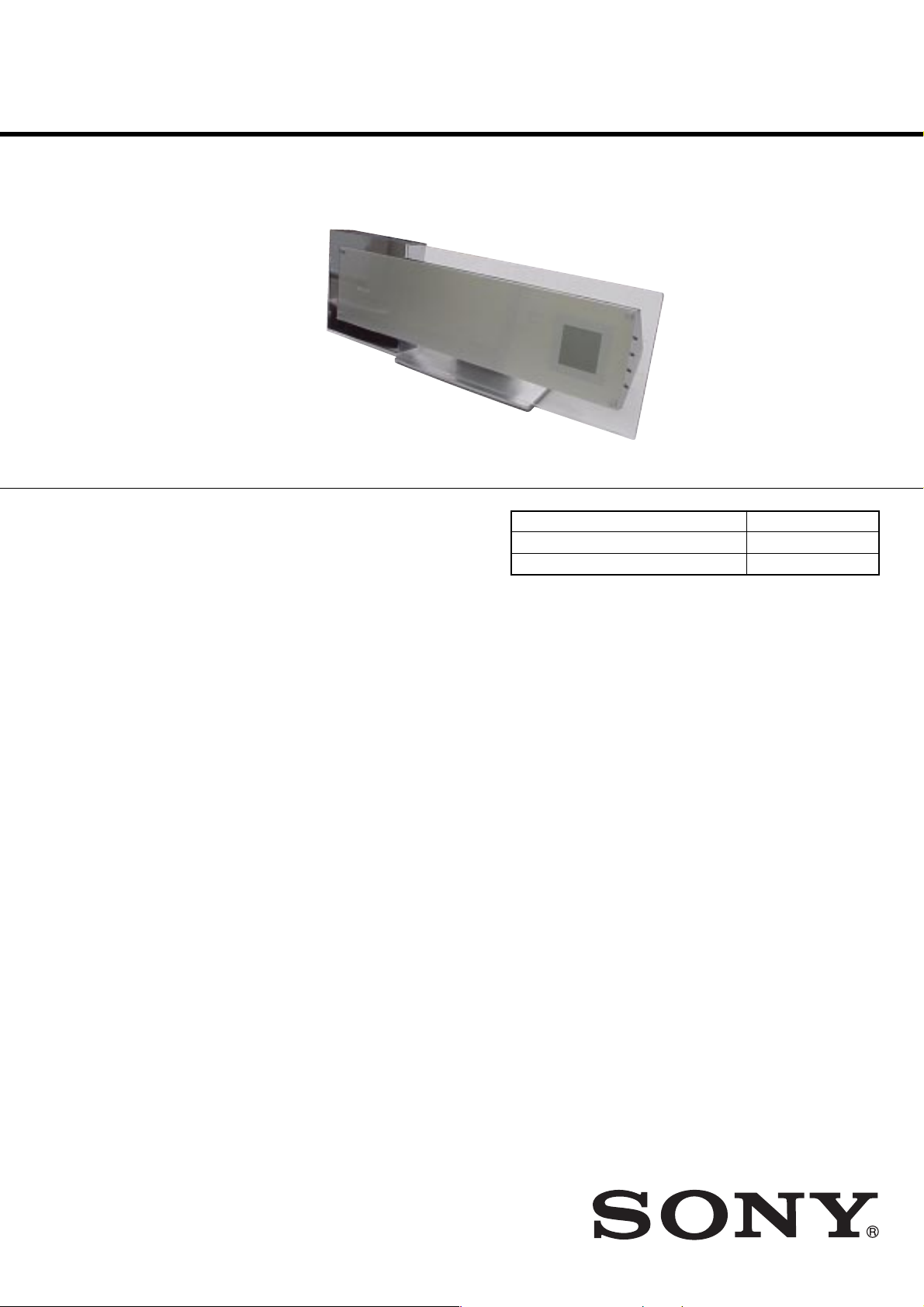
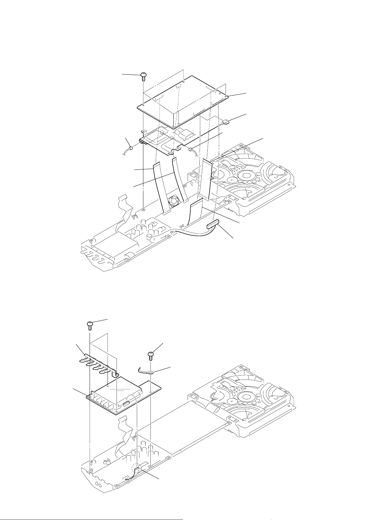
HCD-LF1
SERVICE MANUAL
Ver 1.1 2004.10
• HCD-LF1 is DVD/CD DECK system in DAV-LF1.
* Manufactured under license from Dolby Laboratories.
“Dolby”, “Pro Logic”, and the double-D symbol are trademarks
of Dolby Laboratories.
**Manufactured under license from Digital Theater Systems, Inc.
“DTS”, “DTS-ES”, and “DTS Digital Surround” are trademarks
of Digital Theater Systems, Inc.
SPECIFICATIONS
US Model
Canadian Model
AEP Model
UK Model
E Model
Model Name Using Similar Mechanism NEW
Mechanism T ype CDM80A T-D VBU29T
Optical Pick-up Name DBU-3
Super Audio CD/DVD system
Laser Semiconductor laser
Signal format system
North America,
Latin America: NTSC
Other regions: NTSC, PAL
Frequency response (at 2 CH STEREO mode)
Harmonic distortion Less than 0.03 %
Dimensions (approx.) 568 × 200 × 120 mm
Mass (approx.) 4.7 kg (10 lb 6 oz)
Design and specifications are subject to change
without notice.
(Super Audio CD/DVD: λ
= 650 nm)
(CD: λ = 780 nm)
Emission duration:
continuous
DVD (PCM): 2 Hz to 22
kHz (±1.0 dB)
CD: 2 Hz to 20 kHz (±1.0
dB)
3
(22
/8 × 7 7/8 × 4 3/4
inches) (w/h/d) incl.
projecting parts
9-879-139-02
2004J16-1
© 2004.10
SUPER AUDIO CD/DVD PLAYER
Sony Corporation
Audio Group
Published by Sony Engineering Corporation
Page 2
HCD-LF1
Laser component in this product is capable of emitting radiation
exceeding the limit for Class 1.
This appliance is classified as a
CLASS 1 LASER product.
The CLASS 1 LASER
PRODUCT MARKING is
located on the rear exterior.
CAUTION
Use of controls or adjustments or performance of procedures
other than those specified herein may result in hazardous radiation
exposure.
Notes on chip component replacement
• Never reuse a disconnected chip component.
• Notice that the minus side of a tantalum capacitor may be
damaged by heat.
Flexible Circuit Board Repairing
• Keep the temperature of the soldering iron around 270 °C
during repairing.
• Do not touch the soldering iron on the same conductor of the
circuit board (within 3 times).
• Be careful not to apply force on the conductor when soldering
or unsoldering.
UNLEADED SOLDER
Boards requiring use of unleaded solder are printed with the leadfree mark (LF) indicating the solder contains no lead.
(Caution: Some printed circuit boards may not come printed with
the lead free mark due to their particular size)
: LEAD FREE MARK
Unleaded solder has the following characteristics.
• Unleaded solder melts at a temperature about 40 °C higher
than ordinary solder.
Ordinary soldering irons can be used but the iron tip has to be
applied to the solder joint for a slightly longer time.
Soldering irons using a temperature regulator should be set to
about 350 °C.
Caution: The printed pattern (copper foil) may peel away if
the heated tip is applied for too long, so be careful!
• Strong viscosity
Unleaded solder is more viscou-s (sticky, less prone to flow)
than ordinary solder so use caution not to let solder bridges
occur such as on IC pins, etc.
• Usable with ordinary solder
It is best to use only unleaded solder but unleaded solder may
also be added to ordinary solder.
SAFETY-RELATED COMPONENT WARNING!!
COMPONENTS IDENTIFIED BY MARK 0 OR DOTTED LINE
WITH MARK 0 ON THE SCHEMATIC DIAGRAMS AND IN
THE PARTS LIST ARE CRITICAL TO SAFE OPERATION.
REPLACE THESE COMPONENTS WITH SONY PARTS WHOSE
PART NUMBERS APPEAR AS SHOWN IN THIS MANUAL OR
IN SUPPLEMENTS PUBLISHED BY SONY.
ATTENTION AU COMPOSANT AYANT RAPPORT
LES COMPOSANTS IDENTIFIÉS PAR UNE MARQUE 0 SUR
LES DIAGRAMMES SCHÉMATIQUES ET LA LISTE DES
PIÈCES SONT CRITIQUES POUR LA SÉCURITÉ DE
FONCTIONNEMENT. NE REMPLACER CES COM- POSANTS
QUE PAR DES PIÈCES SONY DONT LES NUMÉROS SONT
DONNÉS DANS CE MANUEL OU D ANS LES SUPPLÉMENTS
PUBLIÉS PAR SONY.
À LA SÉCURITÉ!
• The units that are required for the system operation check during repair service
Units required for
Unit.
need to
checking
DVD player : HCD-LF1
Sub woofer : SA-WSLF1
Front speaker : SS-TSLF1(R)
Center speaker :
SS-CTLF1
Surround speaker : SS-TSLF1W(R)
Remote commander :
RM-SP320
*1 Only the defective unit. *2 Either one of them.
Units with a mark: The units that are required for the system operation check during repair service
However, there can be a case that some units of the system need to not be brought into repair shop depending on the unit. that became defective.
operation
check
SS-TSLF1L(L)
SA-TSLF1(L)
DVD player :
HCD-LF1
aa a
aa a
aaa
aaa a
Sub woofer :
SA-WSLF1
Front speaker :
SS-TSLF1(R)
SS-TSLF1L(L)
*1
*2
Center speaker :
SS-CTLF1
a
Surround speaker :
SS-TSLF1W(R)
SA-TSLF1(L)
*1
a
Remote
commander :
RM-SP320
a
a
2
Page 3

TABLE OF CONTENTS
HCD-LF1
1. SERVICING NOTES ................................................ 4
2. GENERAL ................................................................... 8
3. DISASSEMBLY
3-1. Disassembly Flow ........................................................... 10
3-2. Stand Section ................................................................... 11
3-3. Cover (MAIN/CDM)....................................................... 11
3-4. Chassis Section................................................................ 12
3-5. DLED Board.................................................................... 12
3-6. STBY KEY Board, EJECT KEY Board ......................... 13
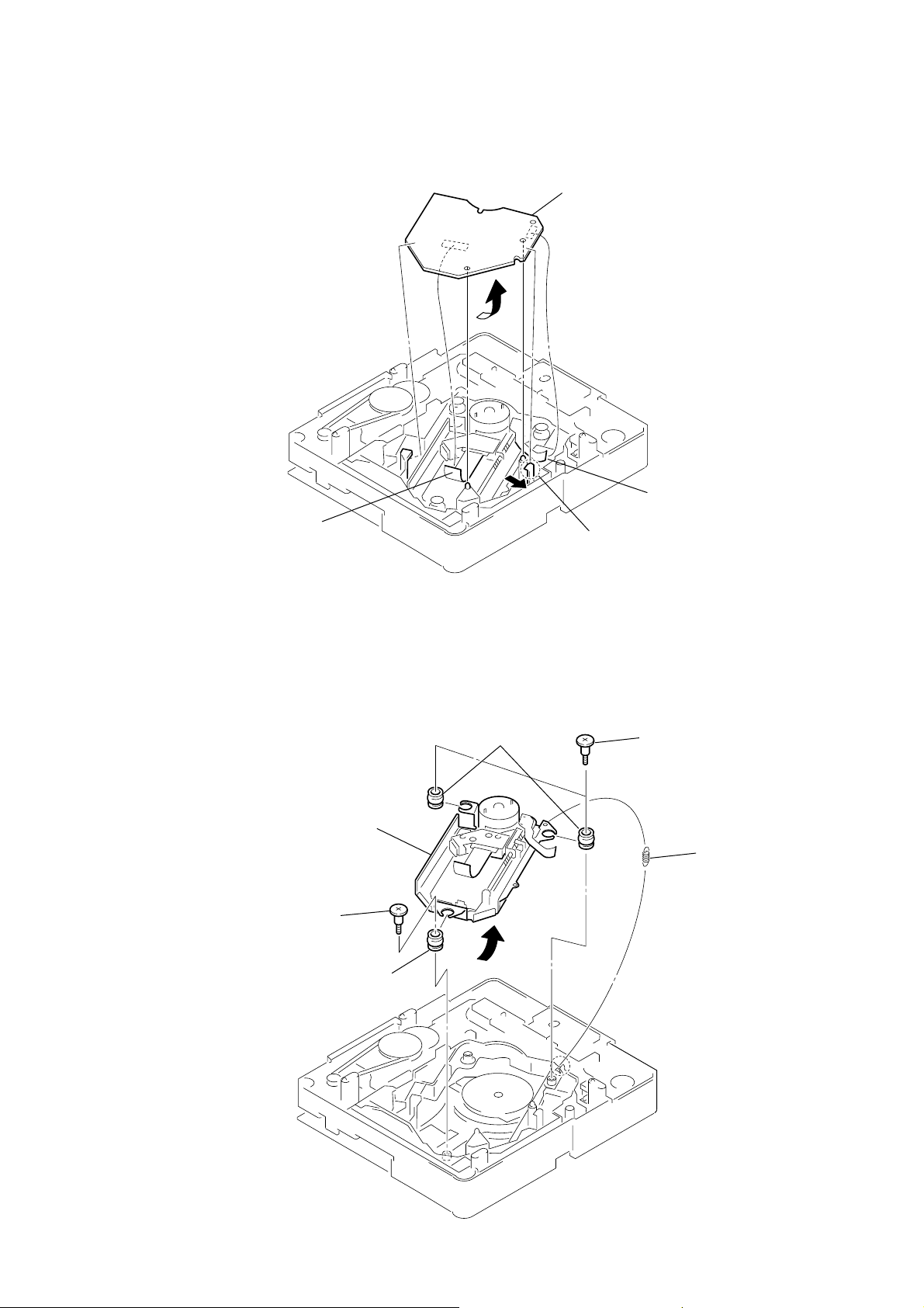
3-7. Mechanism Deck (CDM80AT-DVBU29T)..................... 13
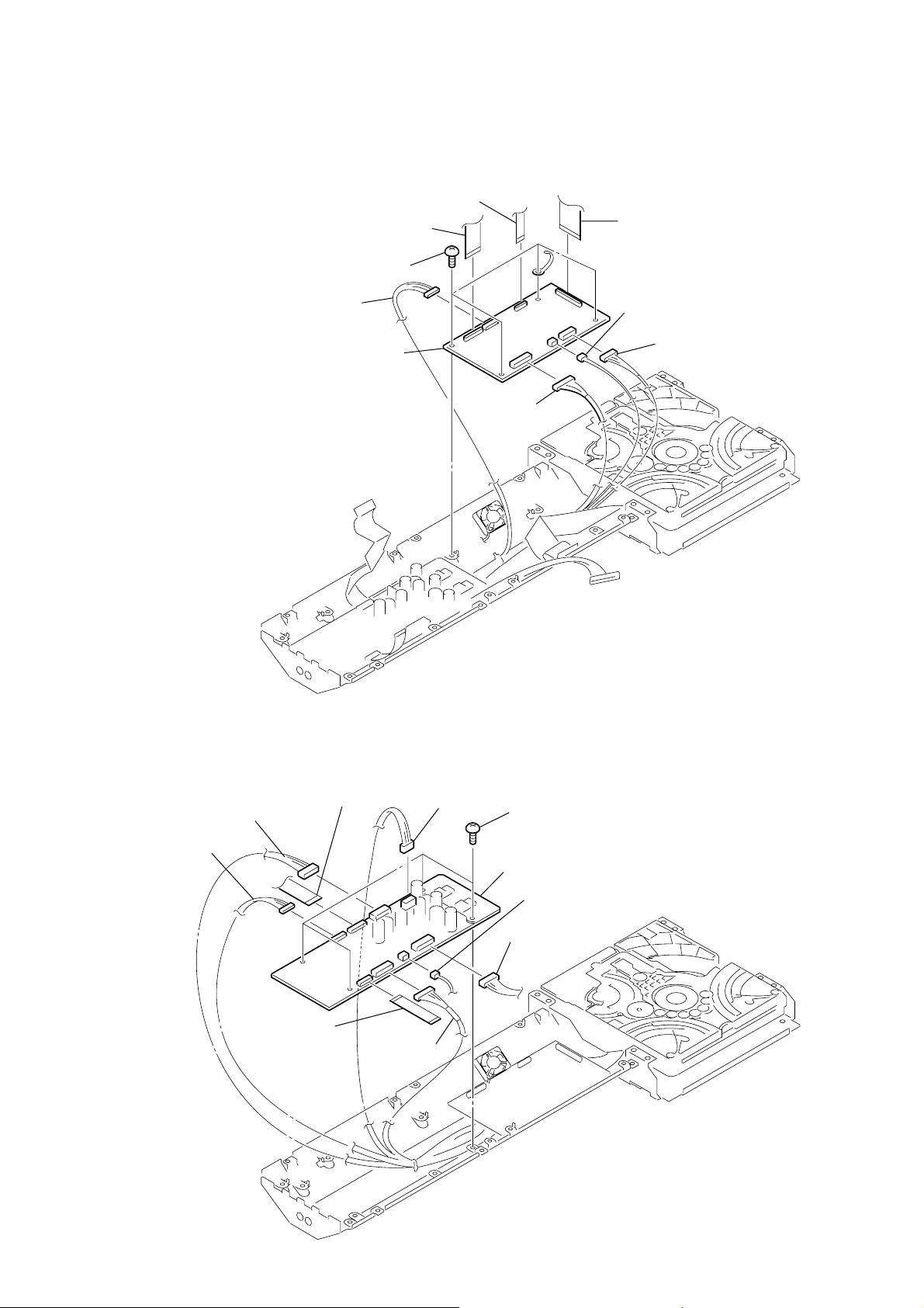
3-8. DMB07 Board ................................................................. 14
3-9. DISPLAY Board .............................................................. 14
3-10. I/O Board ......................................................................... 15
3-11. DVD-POW Board............................................................ 15
3-12. Chassis (Top) ................................................................... 16
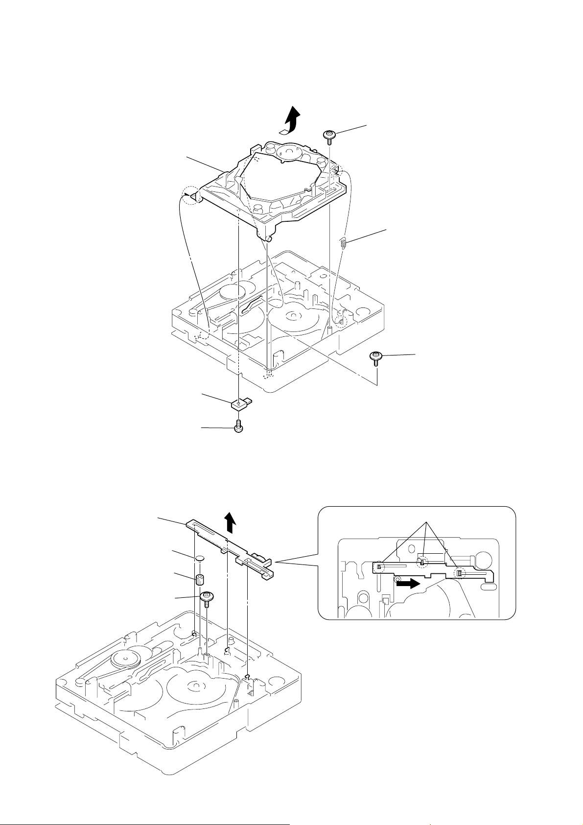
3-13. Lever (Loading R/L)........................................................ 17
3-14. Disc Stop Lever, Disc Sensor Lever ................................ 18
3-15. DRIVER Board ............................................................... 18
3-16. RF Board ......................................................................... 19
3-17. Optical Pick-up (DBU-3) ................................................ 19
3-18. Base Unit ......................................................................... 20
3-19. Lever (BU Lock) ............................................................. 20
3-20. Close Lever...................................................................... 21
3-21. DIR Lever, Gear (IDL-B) ................................................ 21
3-22. Gear (IDL-C) ................................................................... 22
4. TEST MODE ............................................................... 23
5. ELECTRICAL ADJUSTMENTS .......................... 32
6. DIAGRAMS
6-1. Block Diagram — RF SERVO Section — ................... 34
— DVD DSP Section — ................................................. 35
— AUDIO Section —...................................................... 36
— MAIN Section — ....................................................... 37
6-2. Printed Wiring Board — RF Section —......................... 38
6-3. Schematic Diagram — RF Section — ........................... 39
6-4. Printed Wiring Board — DRIVER Section —............... 40
6-5. Schematic Diagram — DRIVER Section — ................. 40
6-6. Printed Wiring Board — DMB07 Section (Side A) — .. 41
6-7. Printed Wiring Board — DMB07 Section (Side B) — .. 42
6-8. Schematic Diagram — DMB07 Section (1/10) — ........ 43
6-9. Schematic Diagram — DMB07 Section (2/10) — ........ 44
6-10. Schematic Diagram — DMB07 Section (3/10) — ........ 45
6-11. Schematic Diagram — DMB07 Section (4/10) — ........ 46
6-12. Schematic Diagram — DMB07 Section (5/10) — ........ 47
6-13. Schematic Diagram — DMB07 Section (6/10) — ........ 48
6-14. Schematic Diagram — DMB07 Section (7/10) — ........ 49
6-15. Schematic Diagram — DMB07 Section (8/10) — ........ 50
6-16. Schematic Diagram — DMB07 Section (9/10) — ........ 51
6-17. Schematic Diagram — DMB07 Section (10/10) — ...... 52
6-18. Printed Wiring Board — DVD-POW Section — ........... 53
6-19. Schematic Diagram — DVD-POW Section (1/2) —..... 54
6-20. Schematic Diagram — DVD-POW Section (2/2) —..... 55
6-21. Printed Wiring Board — DISPLAY Section — ............. 56
6-22. Schematic Diagram — DISPLAY Section — ................ 57
6-23. Printed Wiring Board — TOUCH KEY Section — ....... 58
6-24. Schematic Diagram — TOUCH KEY Section — ......... 59
6-25. Printed Wiring Board — I/O Section — ........................ 60
6-26. Schematic Diagram — I/O Section — ........................... 61
7. EXPLODED VIEWS
7-1. Stand Section................................................................... 84
7-2. Main Section.................................................................... 85
7-3. Chassis Section................................................................ 86
7-4. Mechanism Deck Section-1 (CDM80AT-DVBU29T) .... 87
7-5. Mechanism Deck Section-2 (CDM80AT-DVBU29T) .... 88
7-6. Mechanism Deck Section-3 (CDM80AT-DVBU29T) .... 89
7-7. Base Unit Section ............................................................ 90
8. ELECTRICAL PARTS LIST .................................. 91
3
Page 4

HCD-LF1
SECTION 1
SERVICING NOTES
NOTES ON HANDLING THE OPTICAL PICK-UP BLOCK
OR BASE UNIT
The laser diode in the optical pick-up block may suffer electrostatic
break-down because of the potential difference generated by the
charged electrostatic load, etc. on clothing and the human body.
During repair, pay attention to electrostatic break-down and also
use the procedure in the printed matter which is included in the
repair parts.
The flexible board is easily damaged and should be handled with
care.
NOTES ON LASER DIODE EMISSION CHECK
The laser beam on this model is concentrated so as to be focused on
the disc reflective surface by the objective lens in the optical pickup block. Therefore, when checking the laser diode emission,
observe from more than 30 cm away from the objective lens.
LASER DIODE AND FOCUS SEARCH OPERATION
CHECK
Carry out the “S curve check” in “CD section adjustment” and check
that the S curve waveform is output several times.
NOTE OF REPLACING THE DMB07 BOARD
When replacing the DMB07 board, since the adjustment value is
not set up correctly, “Drive Auto Adjustment” can’t be performed.
In this case, initialize Memory in the following procedures.
Procedure:
1. Set the test mode. (See page 25)
2. Press the [2] ke y of the remote commander, and set the “DRIVE
MANUAL OPERATION”. (See page 27)
3. Press the [6] key of the remote commander, and set the “2-6,
Memory Check”. (See page 29)
4. Press the [CLEAR] key of the remote commander , and initialize
Memory.
NOTE 1: Regarding the notification symbol “R”
Because the number of the operating buttons of this product
are limited, some operations require use of the operating
buttons of the remote commander (RM-SP320 supplied with
the product). When a specific operation requires use of the
operating buttons of the remote commander (RM-SP320), “R”
is added to the specific operating procedure in this manual.
Example MENU/NO “R” The MENU/NO button of remote
commander.
NOTE 2: Incorrect operations may be performed if the test mode is not
entered properly.
In this case, press the ?/1 button to turn the power of f, and
retry to enter the test mode.
DISC TRA Y LOCK
The disc tray lock function for the antitheft of an demonstration
disc in the store is equipped.
Procedure :
1. Press the ?/1 button to turn the set on.
2. Press the FUNCTION “R” button or touch the FUNCTION
button to set DVD function.
3. Insert a disc.
4. While the power is ON (excluding the mode of Power-ON
Animation mode), touch the x Sensor (on T ouch P anel) and
press the A button simultaneously for several seconds.
5. The “Locked” display appears for a while and disc cannot be
removed any more even if the A button is pressed.
*To release this mode, repeat the above operation. The
“Unlocked” display appears and the Disc Tray Lock mode is
canceled.
Note: When “LOCKED” is displayed, the slot lock is not released by
turning power on/off with the ?/1 button.
4
Page 5
CL402
TOUCH KEY BOARD
TOUCH PAD (B) BOARD
TOUCH PAD (A) BOARD
CL403
CL413
CL404
CL414
CL405
CL415
CL416
CL400
CL411
CL401
CL410
CL406
CL412
*
When the TOUCH KEY BOARD is replaced, wire the TOUCH KEY BOARD securely to
the TOUCH PAD (A) BOARD and TOUCH PAD (B) BOARD as shown in the figure.
•NOTE
*
The performance of the main unit can be connected with the remote controller, even if the panel is not connected.
HCD-LF1
•CAUTION-1 (REPLACING THE TOUCH KEY BOARD)
5
Page 6
HCD-LF1
•CAUTION-2 (REPLACING THE CONNECTING CORD)
*
When replacing the connecting cord, fix it at the position in the figure so that the copper conductor of
the cord and the steel plate contact (GND) adequately.
copper conductor of the cord
• SERVICING POSITION-1 (MECHANISM DECK)
*
Connect the DVD-POW BOARD and the MECHANISM DECK with the extension cable, and inspect
the MECHANISM DECK.
extension cable
J-2501-103-A (29P/L300)
connecting cord
MECHANISM DECK
6
Page 7
• SERVICING POSITION-2 (DMB07 BOARD)
*
Connect the I/O BOARD and the DMB07 BOARD by using the three extension cables, and inspect the DMB07 BOARD.
extension cable
J-2501-199-A (25P/L300)
extension cable
J-2501-225-A (9P/L300)
extension cable
J-2501-243-A (17P/L300)
HCD-LF1
I/O BOARD
DMB07 BOARD
7
Page 8
HCD-LF1
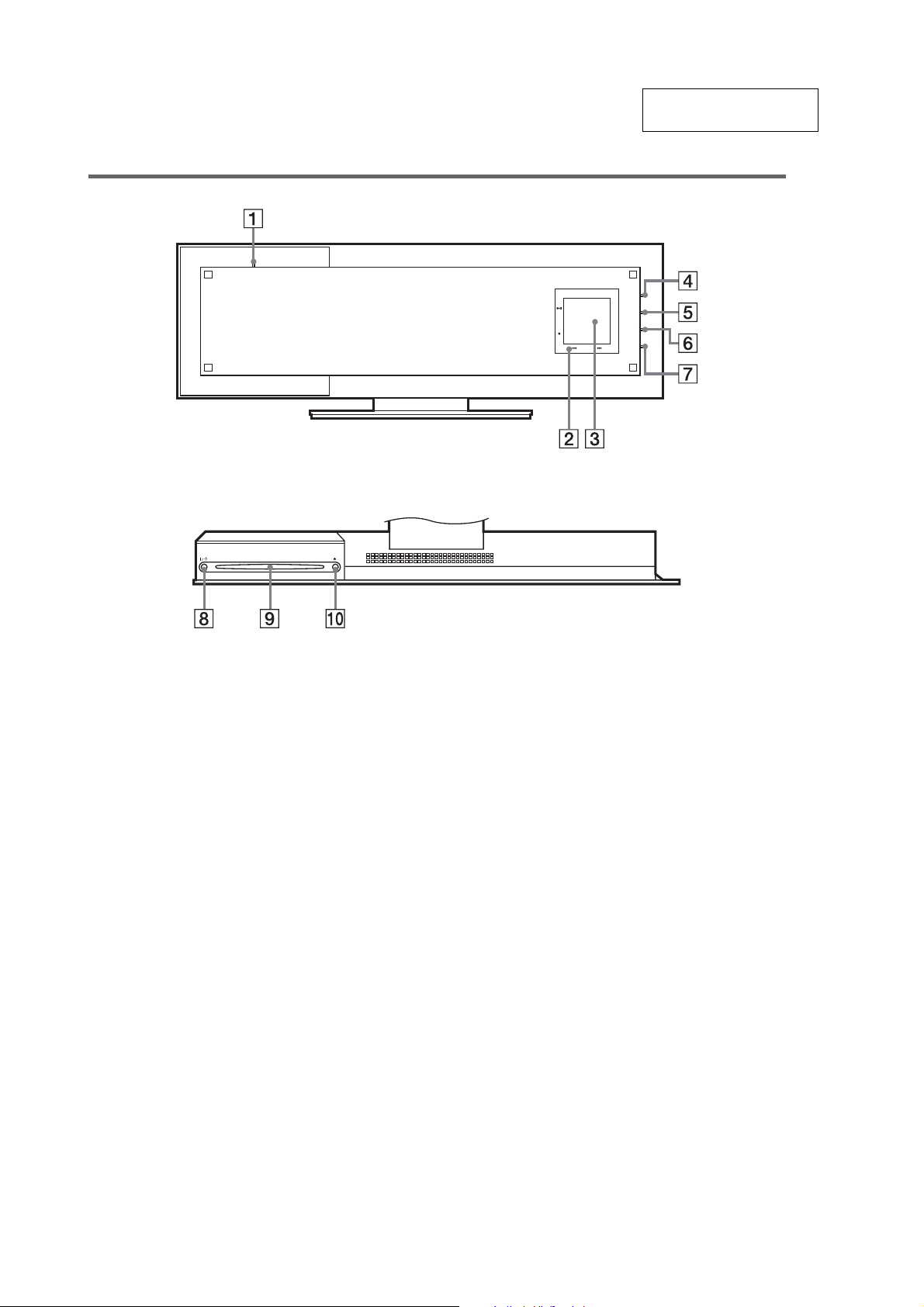
Front Panel
Top Panel
SECTION 2
GENERAL
This section is extracted
from instruction manual.
FUNCTION
+
VOL.
-
A DISC indicator
*
B Touch Panel S ensor (41)
C Front panel display (104)
D DOLBY DIGITAL indicator
E DTS indicator
*
*
F DOLBY PRO LOGIC II indicator
G D.C.S. indicator
*
*Lights up when activated.
H [/1 (power) switch/standby indicator
(39)
I Disc slot (39)
Z (eject) (39)
J
*
8
Page 9
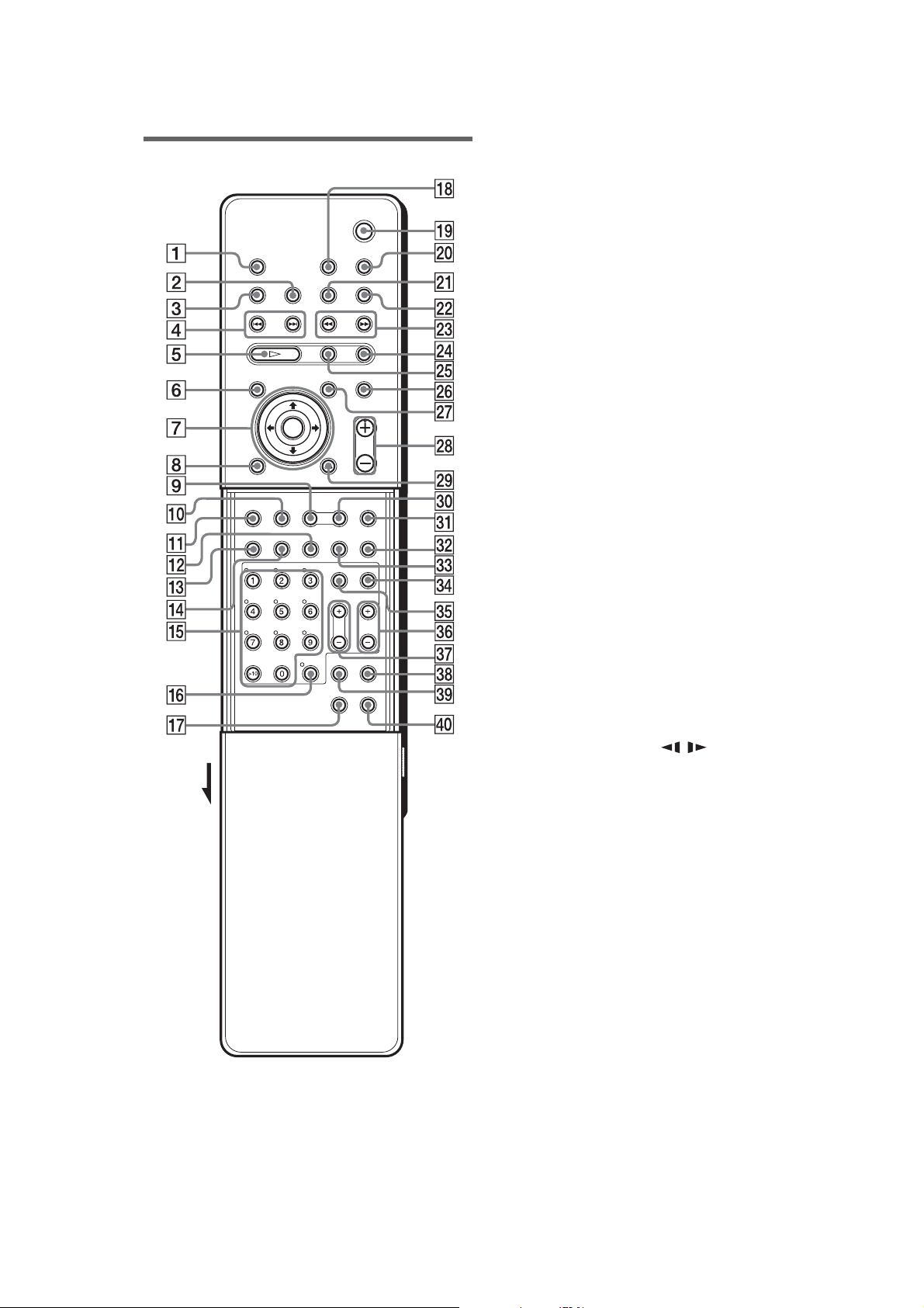
HCD-LF1
Remote
Open the cover.
Note
This remote contr ol glows in the dark. Ho w e ver,
before glowing, the remote must be exposed to light for
awhile.
AZ (eject) (39, 40)
B DISP LA Y (55, 58, 80)
C SLEEP (83)
D ./>, PRESE T –/+ (40, 43, 80, 81)
E H (play) (40, 42, 47, 48, 51, 52)
F DVD TOP MENU/ALBUM– (43, 45, 46)
G C/X/x/c/ENTER (34, 43, 43, 45, 46, 48,
48, 50, 51, 53, 60, 67, 68, 69, 71, 79, 81,
83, 85, 91)
H DVD DISPLAY (45, 46, 50, 51, 53, 58, 59,
60, 67, 68, 69)
I AUTO FORMAT DIRECT (62, 63)
J DSGX (66)
K DVD SETUP (34, 71, 85)
L SUBTITLE (68)
M AUDIO (60)
N ANGLE (67)
O Number buttons (43, 43, 48, 53, 67, 69,
71, 74, 76)
P ENTER
Q TUNER MENU (79, 81)
R TV [/1 (on/standby) (74)
S "/1 (standby) (34, 39, 80)
T SONY TV DIRECT (76)
U TUNER/BAND (79, 80, 81)
V FUNCTION (39, 78, 80, 81)
W m/M/SLOW / , TUNING –/+ (47,
52, 79, 80)
X x (stop) (40, 42, 43, 69, 80)
Y X (pause) (40)
Z MUTING (40)
wj DVD MENU/ALBUM+ (43, 45, 46)
wk VOL +/– (40, 80)
wl O RETURN (43, 45, 46, 48, 53, 69, 71,
85)
e; MODE (63, 64)
ea NIGHT MODE (66)
es PLAY MODE (48, 50)
ed REPEAT (48, 51)
ef TV (74, 76)
eg TV/VIDEO (74, 76)
eh TV CH +/– (74, 76)
ej TV VOL +/– (74)
ek AMP MENU (29, 78, 83, 91)
el CLEAR (34, 48, 53)
r; FM MODE (80)
9
Page 10
HCD-LF1
SECTION 3
DISASSEMBLY
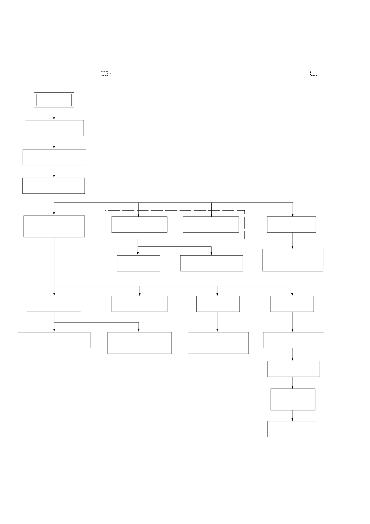
3-1. DISASSEMBLY FLOW
•This set can be disassembled in the order shown below.
•The dotted square with arrow ( ) prompts you to move to the next job when all of the works within the dotted square ( ) are
completed.
SET
3-2.
STAND SECTION
(Page 11)
3-3.
COVER (MAIN/CDM)
(Page 11)
3-4.
CHASSIS SECTION
(Page 12)
MECHANISM DECK
3-7.
(
CDM80AT-DVBU29T)
(Page 13)
. CHASSIS (TOP)
3-12
(Page 16)
. LEVER (LOADING R / L)
3-13
(Page 17)
3-8
. DMB07 BOARD
(Page 14)
. I/O BOARD
3-10
(Page 15)
3-15
. DRIVER BOARD
(Page 18)
3-14
. DISC STOP LEVER,
DISC SENSOR LEVER
(Page 18)
3-9
. DISPLAY BOARD
(Page 14)
3-11
. DVD-POW BOARD
(Page 15)
. RF BOARD
3-16
(Page 19)
3-17
. OPTICAL PICK-UP
(DBU-3)
(Page 19)
3-5
. DLED BOARD
(Page 12)
6.STBY KEY BOARD,
3-
EJECT KEY BOARD
(Page 13)
3-18
. BASE UNIT
(Page 20)
3-19
. LEVER (BU LOCK)
(Page 20)
. CLOSE LEVER
3-20
(Page 21)
3-21
. DIR LEVER,
GEAR (IDL-B)
(Page 21)
10
. GEAR (IDL-C)
3-22
(Page 22)
Page 11
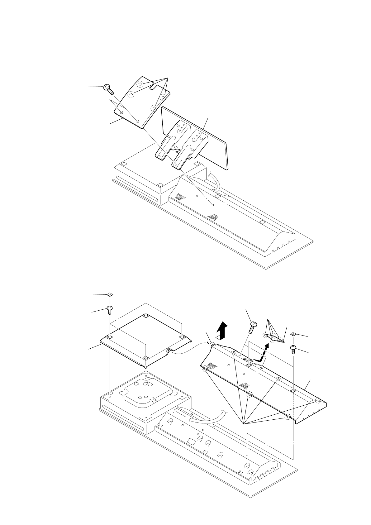
3-2. STAND SECTION
q;
four screws
(+BVTP 3 × 8)
qa
cover (CDM)
1
two covers (SH)
9
four covers (SH)
8
cover (MAIN)
2
two screws
(+BVTP 3 × 8)
3
two screws
6
four claws
4
six claws
5
hook
7
cover (SYS)
1
two screws
×
(HEX 4
10)
3
cover (rear)
2
four claws
4
stand section
HCD-LF1
3-3. COVER (MAIN/CDM)
11
Page 12
HCD-LF1
)
3-4. CHASSIS SECTION
1
4
four screws
(+BVTP 2.6 × 8)
8
chassis section
screw
(+BVTP 3
2
screw
×
8)
+BV3 (3-CR)
3
side panel (CDM)
5
six screws
(+BVTP 3 × 8)
6
four dowels
3-5. DLED BOARD
4
connector (3p)
5
DLED board
3
two dowels
2
indicator (DISC)
1
hook
7
wire (flat type)
(18core) (CN401
12
Page 13
3-6. STBY KEY BOARD, EJECT KEY BOARD
)
)
6
two hooks
qa
escutcheon assy
3
connector (2p)
q;
EJECT KEY board
8
two screws
(+BVTP 2.6
7
bracket (escutcheon)
×
5
8)
two dowels
2
connector (4p)
9
STBY KEY board
1
two screws
(+BVTP 2.6
4
two screws
(+BVTP 2.6
HCD-LF1
×
8)
×
8
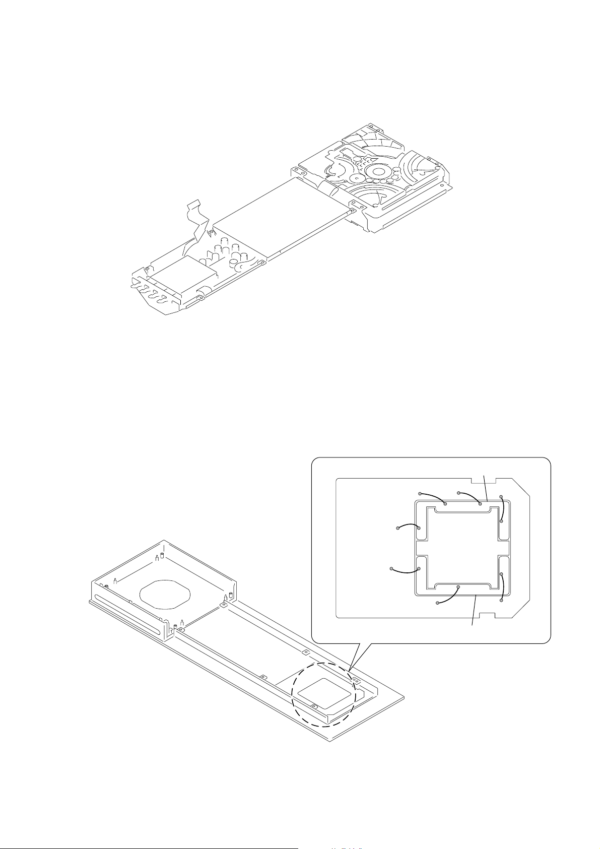
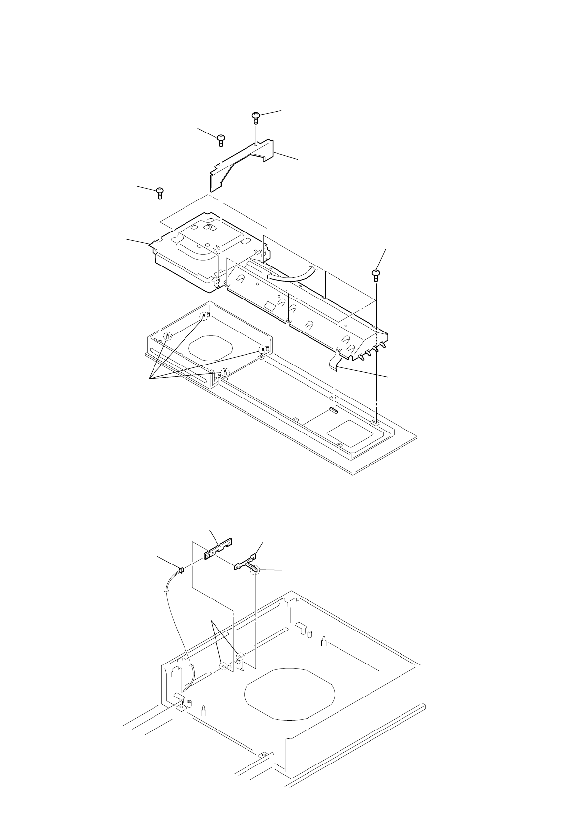
3-7. MECHANISM DECK (CDM80AT-DVBU29T)
3
connector
(7p) (CN701)
2
wire (flat type)
(29core)
4
mechanism deck
(CDM80AT-DVBU29T
1
four screws
(+BVTP 3
×
8)
13
Page 14
HCD-LF1
3-8. DMB07 BOARD
1
five screws
(+BVTP 3
2
wire (flat type)
(17core) (CN105)
3
wire (flat type)
(13core) (CN101)
×
8)
8
connector
(2p) (CN401)
7
q;
9
connector
(2p) (CN402)
DMB07 board
heat sink (DMB)
4
wire (flat type)
(25core) (CN107)
3-9. DISPLAY BOARD
2
indicator (FUNC)
6
DISPLAY board
1
three screws
(+BVTP 3
5
wire (flat type)
(29core) (CN501)
6
connector
(13p) (CN102)
×
8)
3
screw
(+BVTP 3
4
×
8)
clamp (L35)
14
5
wire (flat type)
(12 core) (CN451)
Page 15
3-10. I/O BOARD
8
wire (flat type)
(17core) (CN201)
1
four screws
(+BVTP 3 × 8)
2
connector
(12p) (CN203)
9
I/O board
7
wire (flat type)
(9core) (CN204)
3
(8p) (CN202)
connector
6
wire (flat type)
(25core) (CN101)
4
connector
(2p) (CN103)
5
connector
(7p) (CN102)
HCD-LF1
3-11. DVD-POW BOARD
5
connector
(7p) (CN305)
6
connector
(14p) (CN302)
7
wire (flat type)
(12 core) (CN303)
9
wire (flat type)
(18 core) (CN304)
4
connector
(4p) (CN902)
2
connector
(9p) (CN301)
1
four screws
(+BVTP 3
q;
DVD-POW board
3
connector
(2p) (CN910)
8
connector
(8p) (CN901)
×
8)
15
Page 16
HCD-LF1
)
3-12. CHASSIS (TOP)
3
two screws
(+P 2
5
chassis (top)
4
three screws
(+BVTP 2.6
×
10)
1
×
8)
screw
(+BVTP 2.6
2
lever (CL UP2
×
8)
16
Page 17
3-13. LEVER (LOADING R/L)
HCD-LF1
5
lever (loading R)
1
spr-T (loading L) spr-T (loading R)
4
two hooks
1
2
two hooks
3
lever (loading L)
PRECAUTION DURING LEVER (LOADING R / L) INSTALLATION
Align the horizontal position.
lever (loading L)
Install the
both levers so that they move symmetrically.
lever (loading R)
17
Page 18
HCD-LF1
)
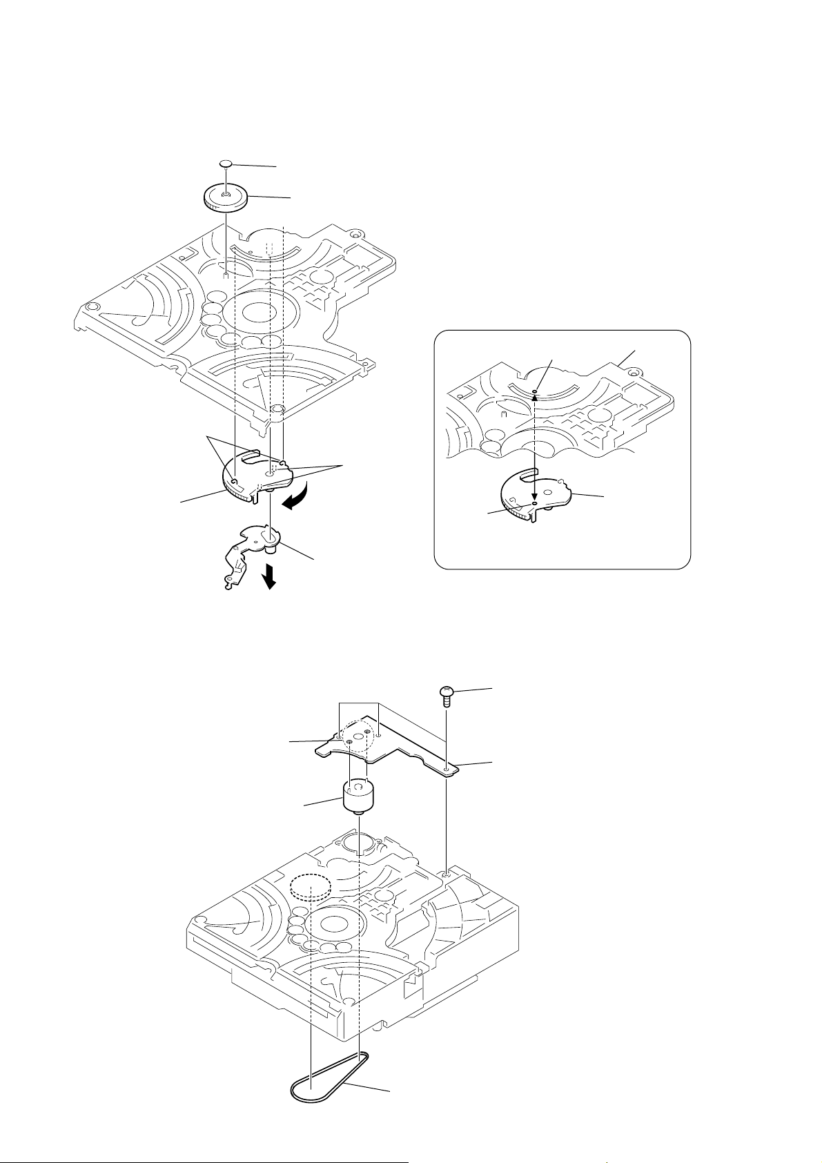
3-14. DISC STOP LEVER, DISC SENSOR LEVER
1
gear (cap)
2
gear (IDL L)
PRECAUTION DURING DISC STOP LEVER INSTALLATION
5
two hooks
6
disc stop lever
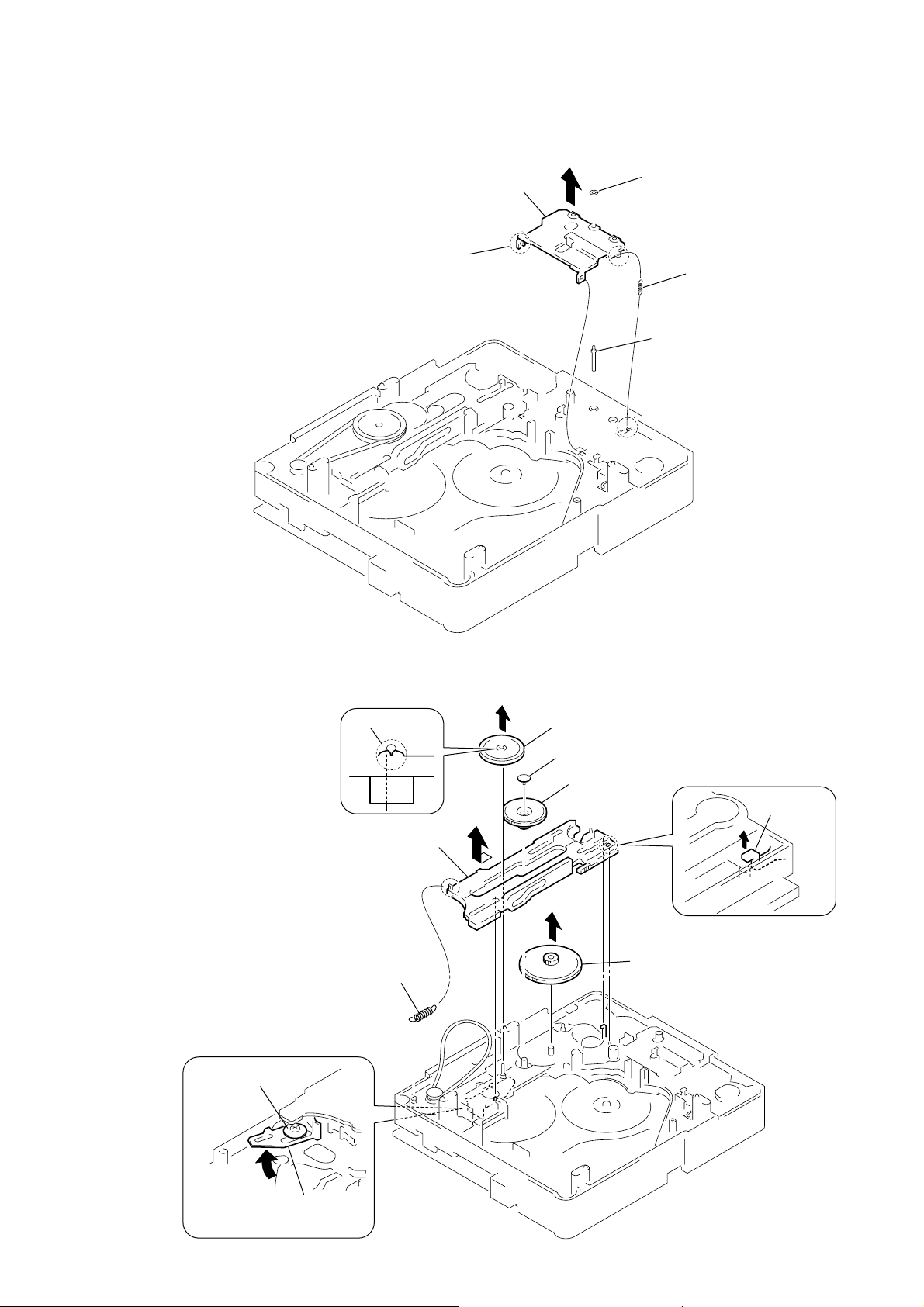
3-15. DRIVER BOARD
3
Remove soldering
from the two points.
3
two claws
4
disc sensor lever
hole
hole
Install the disc stop lever so that the both holes
are aligned.
2
three screws
(+BVTP 2.6
5
DRIVER board
chassis (top)
disc stop lever
×
8
18
4
motor (pully) assy
1
belt (MOT)
Page 19
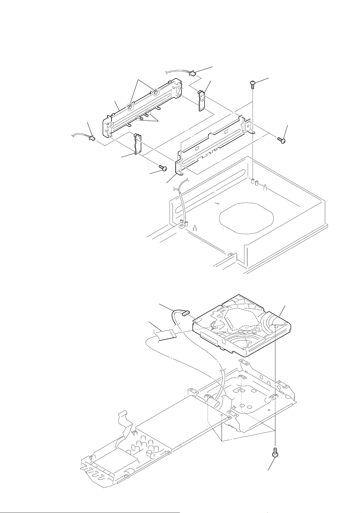
3-16. RF BOARD
4
RF board
HCD-LF1
3
wire (flat type)
(CN001)
3-17. OPTICAL PICK-UP (DBU-3)
6
optical pick-up
(DBU-3)
2
step screw (M)
3
two insulators (RB)
1
claw
2
wire (flat type)
(CN003)
1
two step screws (M)
5
tension coil spring (H-1)
4
insulator
19
Page 20
HCD-LF1
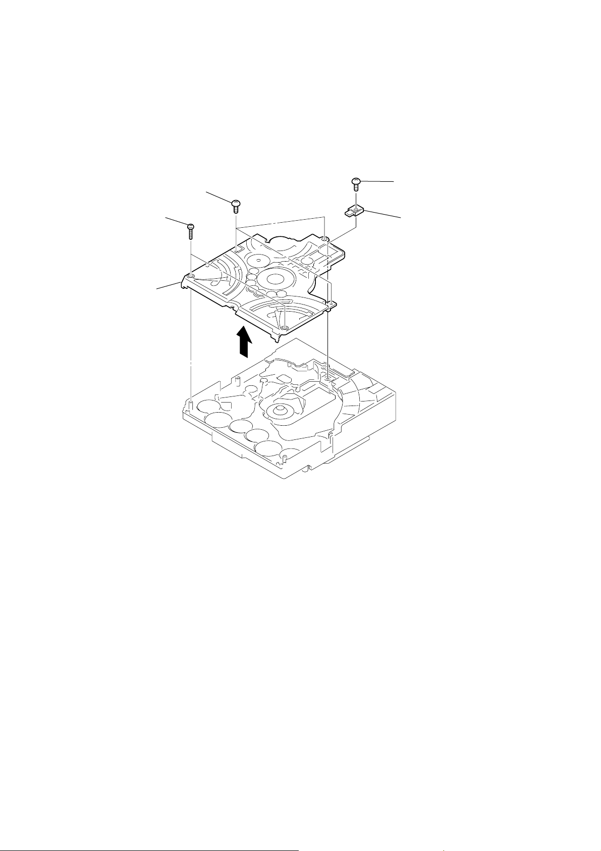
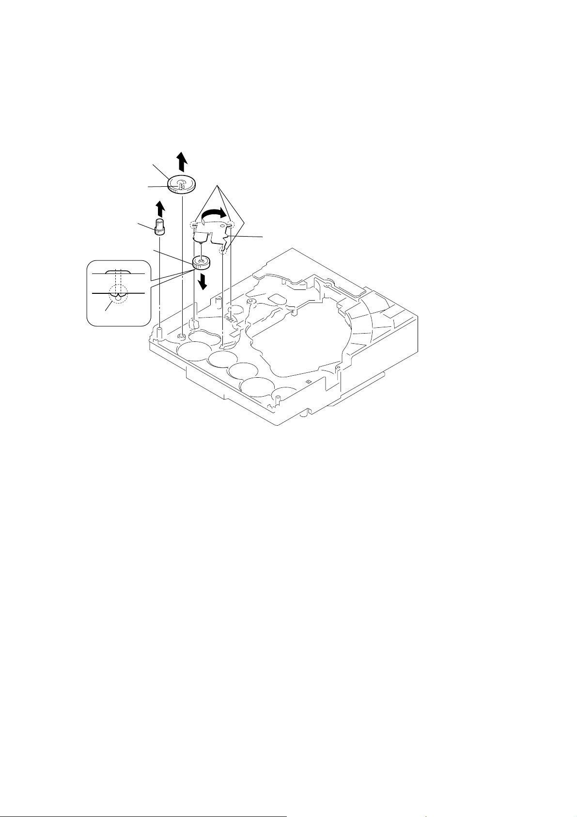
3-18. BASE UNIT
6
base unit
4
floating screw
(+PTPWHM 2.6)
3
holder down spring
1
3-19. LEVER (BU LOCK)
6
lever (BU lock)
1
2
gear (BU lock)
3
floating screw
(+PTPWHM 2.6)
2
lever (CL UP2)
screw
(+BVTP 2.6
gear (cap)
5
floating screw
(+PTPWHM 2.6)
×
8)
5
three hooks
4
20
Page 21
3-20. CLOSE LEVER
3
claw
5
close lever
1
washer (3-1-0.4)
2
4
shaft disc stop
HCD-LF1
close lever spring
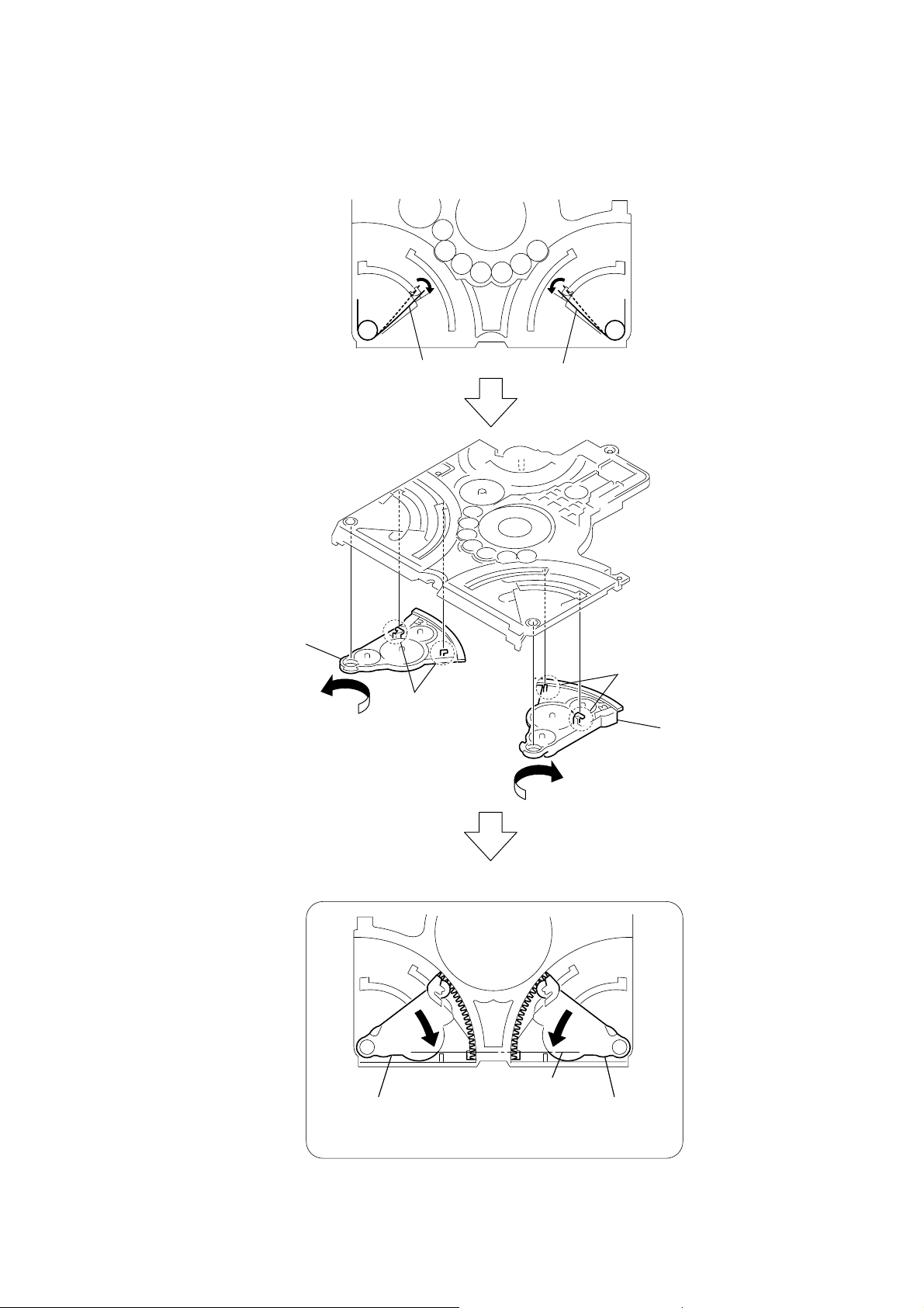
3-21. DIR LEVER, GEAR (IDL-B)
6
Loosen the screw.
2
1
DIR spring
claw
9
DIR lever
3
gear puley
4
gear (cap)
5
gear (IDL-A)
q;
gear (IDL-B)
8
stopper
7
Hold the release lever
and change the direction.
21
Page 22
HCD-LF1
3-22. GEAR (IDL-C)
3
2
1
gear (IDL-F)
7
gear (IDL-C)
gear (IDL-D)
two claws
4
three hooks
5
gear loading lever
6
claw
22
Page 23
SECTION 4
TEST MODE
HCD-LF1
Note 1:Regarding the notification symbol “R”
Because the number of the operating buttons of this product are
limited, some operations require use of the operating buttons of
the remote commander (RM-SP320 supplied with the product).
When a specific operation requires use of the operating buttons
of the remote commander (RM-SP320), “R” is added to the
specific operating procedure in this manual. Example
MENU/NO “R” The MENU/NO button of remote commander .
Note 2:Incorrect operations may be performed if the test mode is not
entered properly.
In this case, press the ?/1 button to turn the power off, and
retry to enter the test mode.
1. Cold Reset
• The cold reset clears all data including preset data stored in
the RAM to initial conditions. Execute this mode when
returning the set to the customers.
Procedure:
1. Press the ?/1 button to turn the power on.
2. While the power is ON (excluding the mode of Power-ON
Animation mode), press the V OL – Sensor (on Touch Panel)
and the press the A button simultaneously for several seconds.
3. The “Cold Reset” display appears for a while, then “Standby”
display flashes, and finally enters “Power Off” (Standby
Mode).
2. Disc Tray Lock
The disc tray lock function for the antitheft of an demonstration
disc in the store is equipped.
Procedure :
1. Press the ?/1 button to turn the set on.
2. Press the FUNCTION “R” button or touch the FUNCTION
button to set DVD function.
3. Insert a disc.
4. While the power is ON (excluding the mode of Power-ON
Animation mode), touch the
x Sensor (on T ouch P anel) and
press the A button simultaneously for several seconds.
5. The “Locked” display appears for a while and disc cannot be
removed any more even if the A button is pressed.
*To release this mode, repeat the above operation. The
“Unlocked” display appears and the Disc Tray Lock mode is
canceled.
Note: When “LOCKED” is displayed, the slot lock is not released by
turning power on/off with the ?/1 button.
3. DVD Ship Mode
•This mode moves the optical pick-up to the position durable
to vibration. Use this mode when returning the set to the
customer after repair.
Procedure:
1. Press the ?/1 button to turn the set on.
2. While the power is ON (excluding the mode of Power-ON
Animation mode), press the FUNCTION “R” button to set
the function “DVD”.
3. Remove the disc.
4. Touch the > Sensor (on Touch Panel) and press the A
button simultaneously for sever al seconds with no disc inserted
in the drive.
5. The “Mecha Lock” display appears for a while, then “Standby”
display blinks, and finally enters “Power Off” (Standby Mode).
* If this operation is performed while the disc is inserted, “Not
In Use” display appears.
4. TEST MODE
The test mode is prepared in this product. Refer to item 5. TEST
MODE IN for the procedure how to enter the test mode, and to item
6. TEST MODE Advance to advance the test mode menu.
Note: Be sure to turn OFF the power of the product after the following
test mode is completed.
[TEST MODE menu]
Version Information
Key Test Mode
Display Test Mode
AMP Test Volume
Repeat Limit
DVD Service
Product Out
VACS ON/OFF
VACS Display
Touch Sensor Test
5. TEST MODE IN
1. When the product is already disassembled for repair, enter the
test mode as follows. Press the TEST MODE key (S301) inside
the product to enter the TEST MODE.
2. To enter the TEST MODE by the external operation (i.e., to
enter the TEST MODE after the product is already reassembled upon completion of repair), press the seven Touch
Sensors in turn while pressing the A button.
Note: Using the TEST MODE IN function by the external operation is
available only for the equipment with the production number of
10450 and onward.
6. TEST MODE MENU Advance
1. Press the TEST MODE key (S301) inside the product to
advance the TEST MODE MENU.
2. If the product is already set in the TEST MODE, the MENU
can be advanced by pressing the RETURN O “R” button.
Note: The MENU advance function using the remote control is av ailable
only for the equipment with the production number of 10450 and
onward.
7. V ersion Information
Procedure:
1. Press the TEST MODE key (S301) inside the product or the
RETURN O “R” button.
2. The version is displayed in order of GC, STR, DVD, and
AREA.
23
Page 24

HCD-LF1
8. Key Test Mode
Procedure:
1. Press the TEST MODE key (S301) inside the product or the
RETURN O “R” button.
2. The message “Key Test” is displayed.
3. Press the ENTER “R” button while the message “Key Test”
is being displayed. The message “Key Number 0” is displayed.
4. Each time a button is pressed, the key number increases.
5. The key test reaches its end when the “Key Number 2” is
displayed.
9. Display Test Mode
Procedure:
1. Press the TEST MODE key (S301) inside the product or the
RETURN O “R” button.
2. The message “Display Test” is displayed.
3. Press the ENTER “R” button while the message “Display
Test” is being displayed. The Display Test Mode is activated.
4. Each time the TEST MODE key (S301) is pressed, the display
changes as follows: (This operation cannot be performed
externally.)
All lights off t All lights on t Displays light on alternately
Illuminate alternately t All lights off
10. AMP Test Volume
1. Press the TEST MODE key (S301) inside the product or the
RETURN O “R” button.
2. The message “Amp Test Volume” is displayed.
3. Press the ENTER “R” button while the message “ Amp Test
Volume” is being displayed. The message “Amp Test Volume
Min” is displayed.
4. Each time the b “R” button is pressed, display changes as
follows:
Min(0) t Cen (20) t Max (40) t Min (0)
14. V A CS ON/OFF
1. Press the TEST MODE key (S301) inside the product or the
RETURN O “R” button.
2. The message “VACS On/Off” is displayed.
3. Press the ENTER “R” button while the message “VACS On/
Off” is being displayed. Either the message “VACS On” or
“VACS Off” is displayed.
4. Select either “VACS On” or “VACS Off” by the b “R” key.
5. After this check is completed, make sure to return the set to
“VACS On”.
15. V A CS Display
1. Press the TEST MODE key (S301) inside the product or the
RETURN O “R” button.
2. The message “VACS Display” is displayed.
3. Press the ENTER “R” button while the message “VACS
Display” is being displayed. “VACS * ” is displayed, where
“*” represents numeric value.
4. If “V A CS Off” is selected in step 14, “VACS Of f” is displayed.
16. T ouch Sensor Test
1. Press the TEST MODE key (S301) inside the product or the
RETURN O “R” button.
2. “QT SCAN” is displayed with the numbers of 0 to 9 after the
character.
3. Press the T ouch sensor while a number in the range of 0 to 9 is
being displayed. The asterisk (*) is displayed next to the
corresponding number when a touch sensor is touched.
11. Repeat Limit
Procedure:
1. Press the TEST MODE key (S301) inside the product or the
RETURN O “R” button.
2. The message “Repeat Limit” is displayed.
3. Press the ENTER “R” button while the message “Repeat
Limit” is being displayed. The message “Repeat Limit
Command Out” is displayed.
4. Press the ENTER “R” button while the message “Repeat
Limit Command Out” is being displayed. The message “Limit
Off” is displayed.
12. DVD Service
Procedure:
1. Press the TEST MODE key (S301) inside the product or the
RETURN O “R” button.
2. The message “DVD Service” is displayed.
3. Press the ENTER “R” button while the message “DVD
Service” is being displayed. The message “DVD Service On”
is displayed.
4. Press the ENTER “R” button while the message “DVD
Service On” is being displayed. After a while, the message
“SERVICE IN” is displayed, and “TEST MODE MENU” is
then displayed on the on-screen display (OSD).
13. Product Out
This function is not available outside the factory. Please skip over
this mode.
24
Page 25

HCD-LF1
### Syscon Diagnosis ###
Diag All Check
No.2 Version
2-2. Version
ROM Revision = X.XX
Press NEXT Key to Continue
Press PREV Key to Repeat
DVD SECTION
[GENERAL DESCRIPTION]
The T est Mode allows you to make diagnosis and adjustment easily
using the remote commander and monitor TV. The instructions,
diagnostic results, etc. are given on the on-screen display (OSD).
[TEST DISC LIST]
Use the following test disc on test mode.
TDV-520CSO (DVD-SL): PART No. J-2501-236-A
LUV-P01 (CD): PART No. 4-999-032-01
TDV-540C (DVD-DL): PART No. J-2501-235-A
Note: Do not use exiting test disc for DVD.
[STARTING TEST MODE]
1. Press the TEST MODE key (S301) inside the product or the
RETURN O “R” button.
2. The message “DVD Service” is displayed.
3. Press the ENTER “R” button while the message “DVD
Service” is being displayed. The message “D VD Service On”
is displayed.
4. Press the ENTER “R” button while the message “DVD
Service On” is being displayed. After a while, the message
“SER VICE IN” is displayed, and displays the T est Mode Menu
on the monitor screen as follows. (At the bottom of the menu
screen, the model name and revision number are displayed)
Test Mode Menu
0. Syscon Diagnosis
1. Drive Auto Adjustment
2. Drive Manual Operation
3. Mecha Aging
4. Emergency History
5. Mecha Error History
6. Version Information
7. Video Level Adjustment
Exit: POWER Key
Model :DAV-LF1
Revision :x.xx
[OPERATING TEST MODE]
0. SYSCON DIAGNOSIS
The same contents as board detail check by serial interface can be
checked from the remote commander operation.
On the Test Mode Menu screen, press 0 “R” key on the remote
commander, and the following Check Menu will be displayed.
### Syscon Diagnosis ###
Check Menu
0. Quit
1. All
2. Version
3. EEPROM
4. GPIO
5. SD Bus
6. Video
0-0. Quit
Quit the Syscon Diagnosis and return to the Test Mode Menu.
0-1. All (All items continuous check)
This menu checks all diagnostic items continuously. Normally, all
items are checked successively one after another automatically
unless an error is found, but at a certain item that requires judgment
through a visual check to the result, the following screen is displayed
for the key entry.
• Example display
5. To execute each function, select the desired menu and press
its number on the remote commander.
6. To release from test mode, press the ?/1 button and turn the
power off.
For the ROM Check, the check sum calculated by the Syscon is
output, and therefore you must compare it with the specified value
for confirmation.
Following the message, press the [ ] button to go to the next
item, or press the [ ] button to repeat the same operation again.
To quit the diagnosis and return to Check Menu screen, press the
RETURN O “R” key on the remote commander to display Check
Menu.
General Description of Checking Method
Selecting 2 and subsequent items calls the submenu screen of each
item. And selecting 2 and subsequent items executes respective
menus and outputs the results.
For the contents of each submenu, see “Check Items List” as below .
.“R”
> “R”
25
Page 26
HCD-LF1
Check Items List:
0-2. Version
0-2-1. All
0-2-2. Revision
0-2-3. ROM Check Sum
0-2-4. Model Type
0-2-5. Region
0-3. EEPROM Check
0-3-1. Sampling Check
0-3-2. Detail Check
0-4. GP I/O Check
0-5. SD Bus Check
0-6. Video Check
0-2. Version
0-2-2. Revision
The revision number of ROM (IC206) that the program
for the DVD system processor (IC207) is stored.
0-2-3. ROM Check Sum
The check sum of ROM (IC206) that the program for the
DVD system processor (IC207) is stored.
(4 digits hexadecimal number)
0-2-4. Model Type
Model name is displayed. (DAV-LF1)
0-2-5. Region
Model destination code is displayed. (2 digits number)
0-3. EEPROM Check
0-3-1. Sampling Check
EEPROM check at every 64 words.
It compares read data with write data of each address.
When there are discrepancies between two data, it displays
error.
0-3-2. Detail Check
EEPROM check at every 1 word.
It compares read data with write data of each address.
When there are discrepancies between two data, it displays
error.
0-4. GP I/O Check
Pull up/down setting check of the DVD system processor (IC207)
pin 150, 151 and 154 (for clock setting port).
0-5. SD Bus Check
SD bus data check between DVD decoder (IC701) and D-RAM
(IC706).
0-6. Video Check
Output the color bars for video level adjustment.
1. DRIVE AUTO ADJUSTMENT
On the T est Mode Menu screen, press the 1 “R” key on the r emote
commander, and the Adjustment Menu will be displayed.
## Drive Auto Adjustment ##
Adjustment Menu
0. ALL
1. DVD-SL
2. CD
3. DVD-DL
Exit: RETURN
Normally, 0 “R” is selected to adjust DVD (single layer), CD and
DVD (dual layer) in this order . But, individual items can be adjusted
for the case where adjustment is suspended due to an error. In this
mode, the adjustment can be made easily through the operation
following the message displayed on the screen.
The disc used for adjustment must be the one specified for
adjustment.
1-0. ALL
Press the 0 “R” key on the remote commander, and the servo set
data in EEPROM will be initialized. Then, 1. DVD-SL disc, 2. CD
disc and 3. DVD-DL disc are adjusted in this order.
Each time one disc was adjusted, it is ejected. Replace it with the
specified disc following the message. You can f inish the adjustment
by pressing the RETURN O “R” button on the remote commander.
Note: During adjustment of each disc, the measurement for disc type
judgment is made. As automatic adjustment does not judge the disc
type unlike conventional models, take care not to insert wrong type
discs. Also, do not give a shock during adjustment.
1-1. DVD-SL (single layer)
Press the 1 “R” key on the remote commander and insert a DVD
single layer disc following the message. Then the adjustment will
be made through the steps below , then adjusted values will be written
to the EEPROM.
DVD Single Layer Disc Adjustment Steps:
1. Sled tilt reset
2. Disc check memory SL
3. Wait 300 msec
4. Set disc type SL
5. LD on
6. Spindle start
7. Wait 1 sec
8. Focus servo on 0
9. Auto track offset adjust
10. CLVA on
11. Wait 500 msec
12. Tracking on
13. Wait 1 sec
14. Sled on
15. Check CLV on
16. Auto LFO adjust
17. Auto focus offset adjust
18. Auto tilt position adjust
19. Auto focus gain adjust
20. Auto focus offset adjust
26
Page 27

HCD-LF1
21. EQ boost adjust
22. Auto loop filter offset adjust
23. Auto track gain adjust
Search Check
24. 32 track jump forward
25. 32 track jump reverse
26. 500 track jump forward
27. 500 track jump reverse
28. All servo stop
29. EEP copy loop filter offset
1-2. CD
Press the 2 “R” key on the remote commander and insert a CD disc
following the message. Then the adjustment will be made through
the steps below , then adjusted values will be written to the EEPR OM.
CD Adjustment Steps
1. Sled tilt rest
2. Disc check memory CD
3. Wait 500 msec
4. Set disc type CD
5. LD on
6. Spindle start
7. Wait 500 msec
8. Focus servo on 0
9. Auto track offset adjust
10. CLVA on
11. Wait 500 msec
12. Tracking on
13. (TC display start)
14. Wait 1 sec
15. Jitter display start
16. Sled ON
17. Check CLV on
18. Auto loop filter offset adjust
19. Auto focus offset adjust
20. Auto focus gain adjust
21. Auto focus offset adjust
22. EQ boost adjust
23. Auto LFO Adjust
24. Auto track gain adjust
Search Check
25. 32Tj forward
26. 32Tj reverse
27. 500Tj forward
28. 500Tj reverse
29. All servo stop
1-3. DVD-DL (dual layer)
Press the 3 “R” key on the remote commander and insert a DVD
dual layer disc following the message. Then the adjustment will be
made through the steps below, then adjusted values will be written
to the EEPROM.
DVD Dual Layer Disc Adjustment Steps:
1. Sled tilt reset
2. Disc check memory DL
3. Wait 500 msec
4. Set disc type DL
5. LD on
6. Spindle start
7. Wait 1 sec
Layer 1 Adjust
8. Focus servo on 0
9. Auto track offset adjust
10. CLVA on
11. Wait 500 msec
12. Tracking on
13. Wait 500 msec
14. Sled on
15. Check CLV lock
16. Auto loop filter offset adjust, Auto focus adjust
17. Auto focus gain adjust
18. Auto focus offset adjust
19. EQ boost adjust
20. Auto loop filter offset adjust
21. Auto Track Gain Adjust
Search Check
22. 32 track jump forward
23. 32 track jump reverse
24. 500 track jump forward
25. 500 track jump reverse
Layer 0 Adjust
26. Focus jump (L1 t L0)
27. Auto track offset adjust L0
28. CLVA on
29. Wait 500 msec
30. Tracking on
31. Wait 500 msec
32. Sled on
33. Check CLV lock
34. Auto focus filter offset adjust
35. Auto Focus Adjust
36. Auto focus gain adjust
37. Auto focus offset adjust
38. EQ boost adjust
39. Auto Loop Filter Offset
40. Auto track gain adjust
Search Check
41. 32 track jump forward
42. 32 track jump reverse
43. 500 track jump forward
44. 500 track jump reverse
Layer Jump Check
45. Layer jump (L0 t L1)
46. Layer jump (L1 t L0)
47. All servo stop
2. DRIVE MANUAL OPERATION
Note: This mode is used for design, and not used in service fundamentally .
On the T est Mode Menu screen, press the 2 “R” key on the r emote
commander, and the Operation Menu will be displayed. For the
manual operation, each servo on/off control and adjustment can be
executed manually.
## Drive Manual Operation ##
Operation Menu
1. Disc Type
2. Servo Control
3. Track/Layer Jump
4. Non EEPROM Write Adjust
5. EEPROM Write Adjust
6. Memory Check
7. Disc Check Memory
8. Error Rate Display
9. SACD Water Mark
Exit: RETURN
In using the manual operation menu, take care of the following
points. These commands do not provide protection, thus requiring
correct operation. The sector address or time code field is displayed
when a disc is loaded.
27
Page 28
HCD-LF1
Note:
1. Set correctly the disc type to be used on the Disc
Type screen.
2. In case of an alarm, immediately touch the x button
to stop the servo operation, and press the +/1
button to turn the power off.
Basic operation:
(controllable from front panel or remote commander)
+/1 : Power OFF (release the Test Mode)
x : Servo stop
A : Stop and eject/Loading
RETURN O “R” : Return to Operation Menu or Test
Mode Menu
. “R” , > “ R” : Transition between sub modes of
menu
1 “R” to 9 “R” , 0 “R” : Selection of menu items
Cursor V “R” / v “R” : Increase/Decrease in manually
adjusted value
2-1. Disc Type
Disc Type
Disc Type Select
1. Disc Type Auto Check
2. Set Disc Type DVD
3. Set Disc Type CD
4. Set Disc Type Hybrid
FZC Count : The number of times which focus zero cross points
of each layer when lens down.
PI Reference : The average of PI reference voltage. (hexadecimal
number)
PI Peak : PI peak level voltage. It performs only when disc
type judgment is successful. (he xadecimal number)
2-1-2. Disc Type DVD
It sets up so that it may judge as a disc type of specification of the
disc with which the set was inserted.
[1]: DVD single layer disc (12 cm)
[2]: DVD dual layer disc (0 layer, 12 cm)
[3]: DVD dual layer disc (1 layer, 12 cm)
[4]: DVD-RW disc (12 cm)
[5]: DVD single layer disc (8 cm)
[6]: DVD dual layer disc (0 layer, 8 cm)
[7]: DVD dual layer disc (1 layer, 8 cm)
[8]: DVD-RW disc (8 cm)
2-1-3. Disc Type CD
It sets up so that it may judge as a disc type of specification of the
disc with which the set was inserted.
[1]: CD disc (normal speed, 12 cm)
[2]: CD disc (double speed, 12 cm)
[3]: CD disc (normal speed, 8 cm)
[4]: CD disc (double speed, 8 cm)
[5]: CD-RW disc (normal speed, 12 cm)
[6]: CD-RW disc (double speed, 12 cm)
[7]: CD-RW disc (normal speed, 8 cm)
[8]: CD-RW disc (double speed, 8 cm)
Exit: RETURN
2-1-1. Disc Type Auto Check
1) Press the 1 “R” ke y on the remote commander to display the
Disc T ype Auto Check screen.
2) Insert a disc and press the ENTER “R” key on the remote
commander.
3) It judges the type of inserted disc automatically and displays
the disc type and so on as below.
Disc Type Auto Check
Disc Type xx
Layer xx
Mirr Time xx
Mirr Count xx
FZC Count xx
PI Reference xx
PI Peak xx
ENTER.Execute
Exit: RETURN
2-1-4. Disc Type Hybrid
It sets up so that it may judge as a disc type of specification of the
disc with which the set was inserted.
[1]: SACD Hybrid disc (SACD layer, 12 cm)
[2]: SACD Hybrid disc (CD layer, normal speed, 12 cm)
[3]: SACD Hybrid disc (CD layer, double speed, 12 cm)
[4]: SACD Hybrid disc (SACD layer, 8 cm)
[5]: SACD Hybrid disc (CD layer, normal speed, 8 cm)
[6]: SACD Hybrid disc (CD layer, double speed, 8 cm)
2-2. Servo Control
Note: Be sure to perform the disc type setup before performing this item.
Servo Control
1.LD off R.Sled FWD
2.Focus off L.Sled REV
3.SPDL off U.Sled Reset
4.CLVA off D.Sled Limit
5.Trk. off
6.Sled off
7.Fcs.Srch off
8.Fcs.OppL off
0.All Servo Off
Exit: RETURN
Disc Type : CD, DVD or Hybrid (SACD)
Layer : SINGLE, DUAL or HYBRID
Mirr Time : Mirror time of between disc surface and record
surface when disc type judgment. (hexadecimal
number)
Mirr Count : The number of times which mirror counts between
disc surface and record surface when disc type
judging.
28
On this screen, the servo on/off control necessary for replay is
executed. Normally, turn on each servo from 1 sequentially and
when CLVA is turned on, the usual trace mode becomes active. In
the trace mode, DVD sector address or CD time code is displayed.
This is not displayed where the spindle is not locked.
The spindle could run overriding the control if the spindle system is
faulty or RF is not present. In such a case, do not operate CLVA.
Page 29
HCD-LF1
[1] LD : Turn on/off the laser.
[2] Focus : Search the focus and turn on the focus.
[3] SPDL : Turn on/off the spindle.
[4] CLVA : Turn on/off normal servo of spindle servo.
[5] Trk. : Turn on/off the tracking servo.
[6] Sled : Turn on/off the sled servo.
[7] FCS. Srch : Turn on/off the focus search.
[8] FCS. OppL : Turn on/off the focus search to another
(opposite) layer of designated layer in Disc
Type setting. (dual layer disc only)
[0] : All servo off.
[ ] Sled FWD (right cursor) : Move the sled forward.
b
[ ] Sled REV (left cursor) : Move the sled reverse.
B
[ ] Sled FWD (up cursor) : Reset the sled.
V
[ ] Sled REV (down cursor) : Limit in the sled.
v
2-3. Track/Layer Jump
Track/Layer Jump
1. 1Tj FWD
2. 1Tj REV
3.500Tj Fine FWD
4.500Tj Fine REV
5.10kTj Dirc FWD
6.10kTj Dirc REV
7.20kTj Dirc FWD
8.20kTj Dirc REV
0. All Servo Off
[1] Focus Offset : Adjusts focus offset.
[2] Focus Gain : Adjusts focus gain.
[3] TRK. Offset :
side.
[4] TRK. Offset : Adjusts tracking of fset of the DSP (IC509)
side.
[5] TRK. Gain : Adjusts track gain.
[6] EQ Boost: Adjusts amount of boost of equalizer.
[0] : All servo off.
2-5. EEPROM Write Adjust
1. Focus Offset
2. Focus Gain
3. Trk. Offset Coarse
4. --------------------
5. Trk. Gain
6. EQ Boost
0.All Servo Off
On this screen, each item can be adjusted automatically. Select the
desired number 1 “R” to 6 “R” from the remote commander, and
selected item is adjusted automatically.
Adjusts tracking offset of the RF amp (IC001)
EEPROM Write Adjust
Exit: RETURN
Exit: RETURN
On this screen, track jump, etc. can be performed. Only for the DVD
dual layer disc, the focus jump and layer jump are displayed in the
right field
[1] 1Tj FWD : 1 track jump forward.
[2] 1Tj REV : 1 track jump reverse.
[3] 500Tj FWD : 500 track jump (fine search)forward.
[4] 500Tj REV : 500 track jump (fine search) reverse.
[5] 10kTj FWD : 10k track jump (direct search) forward.
[6] 10kTj REV : 10k track jump (direct search) reverse.
[7] 20kTj FWD : 20k track jump (direct search) forward.
[8] 20kTj REV : 20k track jump (direct search) reverse.
[0] : All servo off.
2-4. Non EEPROM Write Adjust
Non EEPROM Write Adjust
1. Focus Offset
2. Focus Gain
3. Trk. Offset Coarse
4. Trk. Offset Fine
5. Trk. Gain
6. EQ Boost
[1] Focus Offset : Adjusts focus offset.
[2] Focus Gain : Adjusts focus gain.
[3] TRK. Offset : Adjusts tracking offset of the RF amp (IC001)
side.
[5] TRK. Gain : Adjusts track gain.
[6] EQ Boost : Adjusts amount of boost of equalizer.
[0] : All servo off.
2-6. Memory Check
Display images are shown as follows, and all two screens are able
to switch by the V “R” key (UP) or v “R” key (DW).
EEPROM Data 1/2 CD SL L0 L1
Focus Gain xx xx xx xx
Trk. Gain xx xx xx xx
Focus Offset xx xx xx xx
Trk. Offset xx xx xx xx
EQ. Boost xx xx xx xx
PI Level xx xx -- -Fcs. Balance -- xx -- -Jitter xx xx xx xx
Mirror Time xx xx xx -FE Level -- xx -- -Traverse Lv1. -- xx -- -Next:DW Default:CLR Exit:RET
0.All Servo Off
Exit: RETURN
On this screen, each item can be adjusted manually. Select the desired
number 1 “R” to 6 “R” from the remote commander, and current
setting for the selected item will be displayed, then increase or
decrease numeric value with the B “R” key or b “R” key. This
value is stored in the EEPROM. If CLV has been applied, the jitter
is displayed for reference for the adjustment.
29
Page 30
HCD-LF1
EEPROM Data 2/2 CDRW DVDRW
Focus Gain xx xx
Trk. Gain xx xx
Focus Offset xx xx
Trk. Offset xx xx
EQ. Boost xx xx
Next:UP Default:CLR Exit:RET
On this screen, current servo adjusted data stored in the EEPROM
are displayed. The adjusted data are initialized by pressing the
CLEAR “R” key, but be careful that they are not recoverable after
initialization.
Before clearing the adjusted data, make a note of the set data. This
screen will also appear if [0] All is selected in the Drive Auto
Adjustment. In this case, default setting cannot be made.
2-7. Disc Check Memory
Disc Check Memory
1. SL Disc check
2. CD Disc check
3. DL Disc check
2-9. SACD Water Mark Check
SACD Water Mark Check
PSP AMP
PSN
Start: ENTER Stop: RETURN
On this screen, measure the PSP AMP v alue and PSN value of SA CD
water mark.
3. MECHA AGING
On the T est Mode Menu screen, selecting 3 “R” displays the aging
test menu.
Note: MECHA AGING is not available in this set.
### Aging Test MENU ###
** Pls use over 40min. CD **
Operation Menu
1. Open/Close Test
Exit: RETURN
On this screen, measure the mirror time of chucked disc, and write
to the EEPROM.
2-8. Error Rate Display
Error Rate Display
UC CR Address
PI1 Err Now xx xxxx xxxxxxxx
Max xx xxxx xxxxxxxx
Avg xx xxxx
PI2 Err Now xx xxxx xxxxxxxx
Max xx xxxx xxxxxxxx
Avg xx xxxx
PO Err Now xx xxxx xxxxxxxx
Max xx xxxx xxxxxxxx
Avg xx xxxx
Start: ENTER Stop: RETURN
On this screen, measure and display the error rate.
UC : Incorrect value
CR : Correct value
Add: Address
Exit: RETURN
4. EMERGENCY HISTORY
On the Test Mode Menu screen, selecting 4 “R” displays the
information such as servo emergency history.
The history information from last 1 up to 10 can be scrolled with
the V “R” key or v “R” key. Also, specific information can be
displayed by directly entering that number with ten keys.
### EMG. History ###
Laser Hours CD xxxxhxxm
DVD xxxxhxxm
a. bb xx xx xx xx xx xx xx
xx xx xx xx xx xx xx xx
a. bb xx xx xx xx xx xx xx
xx xx xx xx xx xx xx xx
Select:1-9 Scroll:UP/DOWN
(1.Latest EMG.) Exit: RETURN
xxxxhxxm : The laser on total hours. Data below minutes are
omitted.
a. : Error number.
bb : Error code.
xx : Not used.
30
Page 31

HCD-LF1
## Version Information ##
IF con. Ver.x. xx
SYScon. Ver.x. xx (xxxx)
Model DAV-LF1
Region 0x
Config xxxxxxxx
xxxxxxxx
Front End Ver.x.xx
Exit: RETURN
• Clearing History Information
Clearing laser hours:
Press the DISPLAY “R” and CLEAR “R” keys in thisorder.
Then both CD and DVD data are cleared.
Clearing emergency history:
Press the TOP MENU “R” and CLEAR “R” keys in this order.
Initializing set up data:
Press MENU “R” and CLEAR “R” keys in this order. The data
have been initialized when “EEPR OM Initialize Finished. ” message
is displayed. The EMG. History screen will be restored soon.
• Code list of Emergency History
10: Communication to RF AMP (IC001) failed.
11: Each servo for focus, tracking, and spindle is unlocked.
12: Check sum error of EEPROM (IC204).
14: Communication to servo DSP (IC509) failed, or servo DSP
(IC509) is faulty.
15: Communication to DVD decoder (IC701) failed, or DVD
decoder (IC701) is faulty.
16: Communication to DSD decoder (IC801) failed, or DSD
decoder (IC801) is faulty.
20: Initialization of sled servo failed. It is not placed in the initial
position.
23: Sled servo operation error.
24: Made a request to move the sled servo to wrong position.
30: Tracking balance adjustment error.
31: Tracking gain adjustment error.
33: Focus bias adjustment error.
34: Focus gain adjustment error.
35: Equalizer adjustment error.
40: Focus servo does not operate.
41: With a DVD dual layer disc, focus jump failed.
50: CLV (spindle) servo does not operate.
51: Spindle does not stop.
60: Made a request to seek nonexistent address.
61: Seek error of retry more than regulated times.
70: Control data could not be read.
80: Disc reading failed.
5. MECHA ERROR HISTORY
On the Test Mode Menu screen, selecting 5 “R” displays the
information of mechanism deck error history.
The history information from last 1 up to 8 can be scrolled with
the V “R” key or v “R” key. Also, specific information can be
displayed by directly entering that number with ten keys.
aa: Initialization is completed or not.
FF : Complete.
other number : Not complete.
bb: Operating status of mechanism deck at an error occurred.
(lod sq jcp)
00 : Initializing.
10 to 15 : Open operating.
16 to 19 : Kicking cause open failed.
1A to 1F : Open operating.
20 to 27 : Complete the open operation.
28 : No disc and complete the open operation.
29 to 2F : Complete the open operation.
30 to 3F : Close requesting.
40 to 4F : Open requesting.
50 to 5F : Close operating.
60 to 6F : Complete the chucking operation.
80 to 8F : Complete the release operation.
(BU is home position)
90 to 9F : BU down operating.
A0 to AF : Opening/closing the shutter. Or stationary state
in open/close the shutter is enablement.
B0 to BF : BU up requesting.
C0 to CF : BU down requesting.
D0 to DF : BU upping.
E0 to EF : No disc checking in disc loading.
cc: Operating status of mechanism deck at an error occurred.
(lod oq jcp)
00 : Complete the operation.
10 to 1F : Open operating.
20 to 2F : Close operating.
30 to 3F : Release operating.
60 to 6F : Chucking operating.
70 to 7F : Kicking operating.
80 to 8F : Returning the BU to home position. (after
kicking)
6. VERSION INFORMATION
On the T est Mode Menu screen, selecting 6 “R” displays the ROM
version and region code.
The parenthesized hexadecimal number in version field is checksum
value of ROM.
### Mecha Error History ###
1. aa bb cc xx xx xx xx xx
2. aa bb cc xx xx xx xx xx
3. aa bb cc xx xx xx xx xx
4. aa bb cc xx xx xx xx xx
5. aa bb cc xx xx xx xx xx
6. aa bb cc xx xx xx xx xx
7. aa bb cc xx xx xx xx xx
8. aa bb cc xx xx xx xx xx
(1.Latest Err.) Exit: RETURN
Scroll:UP/DOWN
IF con. : The version of system controller (IC301).
SYScon. : The version of DVD system processor (IC207).
Front End : The version of mechanism controller (IC901).
7. VIDEO LEVEL ADJUSTMENT
On the T est Mode Menu screen, selecting 7 “R” displays color bars
for video level adjustment. During display of color bars, OSD
disappears but the menu screen will be restored if pressing the
RETURN O “R” key.
31
Page 32

HCD-LF1
Ver 1.1
SECTION 5
ELECTRICAL ADJSTMENT
DVD SECTION
AUTO SERVO ADJUSTMENT
After parts related to the servo circuit (RF amplifier (IC001), DSP
(IC509), motor driver (IC501), EEPROM (IC903) so on) are
replaced, re-adjusting the servo circuit is necessary. Select “ALL”
at “1. DRIVE AUTO ADJUSTMENT” (Refer to page 26 in TEST
MODE) and adjust DVD-SL (single layer), CD and D VD-DL (dual
layer).
[TEST DISC LIST]
Use the following test disc on test mode.
TDV-520CSO (DVD-SL): PART No. J-2501-236-A
LUV-P01 (CD): PART No. 4-999-032-01
TDV-540C (DVD-DL):PART No. J-2501-235-A
Note: Do not use exiting test disc for DVD.
[RFMON Level Check]
By using the special jig (J-2501-272-A), checking RF signal
waveform can carry out easily.
Connection:
RF
GND
J-2501-272-A
CN901
Procedure:
1. Connect an oscilloscope to RF pin and GND pin on the special
jig (J-2501-272-A).
2. Turn the power on.
3. Set the test disc (DVD: TD V-520CSO, CD: LUV -P01) on the
tray and touch the u button to playback.
4. Confirm that oscilloscope waveform is clear and check
RFMON signal level is correct or not.
Note: A clear RFMON signal waveform means that the shape “◊” can be
clearly distinguished at the center of the waveform.
32
RFMON signal waveform
VOLT/DIV: 200 mV
TIME/DIV: 500 ns
±
level: 1.09
0.2 Vp-p (DVD)
1.05
±
0.2 Vp-p (CD)
Page 33

SECTION 6
DIAGRAMS
HCD-LF1
• Circuit Boards Location
STBY KEY board
DRIVER board
DLED board
DMB07 board
RF board
EJECT KEY board
TOUCH PAD (A) board
TOUCH PAD (B) board
I/O board
DVD-POW board
TOUCH KEY board
THIS NOTE IS COMMON FOR PRINTED WIRING BOARDS AND SCHEMATIC DIAGRAMS.
(In addition to this, the necessary note is printed in each block.)
For Schematic Diagrams.
Note:
• All capacitors are in µF unless otherwise noted. (p: pF)
50 WV or less are not indicated except f or electrolytics and
tantalums.
• All resistors are in Ω and 1/
specified.
• f : internal component.
• C : panel designation.
Note:
The components identified by mark 0 or dotted
line with mark 0 are critical for safety.
Replace only with part
number specified.
• A : B+ Line.
• H : Adjustment for repair.
•Voltages and waveforms are dc with respect to ground under no-signal (detuned) conditions.
no mark : DVD STOP
* : Impossible to measure
•Voltages are taken with a VOM (Input impedance 10 MΩ).
Voltage variations may be noted due to normal production
tolerances.
•Waveforms are taken with a oscilloscope.
Voltage variations may be noted due to normal production
tolerances.
• Circled numbers refer to waveforms.
• Signal path.
F : AUDIO
d : TUNER
J : CD PLAY
c : DVD PLAY
I : SACD PLAY
L : VIDEO
E : Y
a : CHROMA
r : COMPONENT VIDEO
q : R, G, B
•Abbreviation
CND : Canadian model.
E41 : Chilean and peruvian models.
EA : Saudi Arabia model.
HK : Hong Kong model.
KR : Korea model.
MX : Mexican model.
RU : Russian model.
SP : Singapore model.
4
W or less unless otherwise
Note:
Les composants identifiés par
une marque 0 sont critiques
pour la sécurité.
Ne les remplacer que par une
piéce portant le numéro
spécifié.
For Printed Wiring Boards.
Note:
• X : parts extracted from the component side.
• a : Through hole.
• f : internal component.
• : Pattern from the side which enables seeing.
(The other layers' patterns are not indicated.)
Caution:
Pattern face side: Parts on the pattern face side seen from
(SIDE A) the pattern face are indicated.
Parts face side: Parts on the parts face side seen from
(SIDE B) the parts face are indicated.
• Indication of transistor.
C
Q
B
E
B
These are omitted.
Q
CE
These are omitted.
HCD-LF1
FAN CONTROL board
DISPLAY board
3333
Page 34

HCD-LF1
6-1. BLOCK DIAGRAM — RF SERVO SECTION —
DETECTOR
OPTICAL PICK-UP
BLOCK
(DBU-3)
LASER
DIODE
(FOR CD)
LASER
DIODE
(FOR DVD)
2AXIS
DEVICE
FOCUS/
TRACKING
(SPINDLE)
COIL
M2
(SLED)
M1
CD LD
DVD LD
INLIM
FCS+
FCS–
TRK+
TRK–
MM
MM
PD
SW
• SIGNAL PATH
FNP
FNN
FF
FR
TF
TR
: AUDIO
: VIDEO
535254
117
RFIN
8
DIP
55
DIN
RFAC
MIN
MEVO
SDATA
SCLK
SDEN
MIRR
VI25
LDON
FF
FR
57
31
32
47
46
48
39
TE
40
FE
38PI
27
36
26
7
FCS_JMP_1
8
FCS_JMP_2
44
SLED_B
43
SLED_A
97
DSAVE
60
MUTE_2D
63
SP_ON
73
TSD-M
62
FG
28
76 31
LDON
LDSEL
3
–
1
+
INLIM
SLED
4
IC003
AMP
DATA_RF
CLK_RF
SDEN
MIRR
AVC
61
TE
FE
PI
TE
FE
PI
CLK_RF
DATA_RF
82
83
SDCLK_RF
SDATA_RF
IC503
SDEN
2
SDEN
AMP
50
RFAC
IC509
CD DECODER,
DIGITAL SERVO PROCESSOR
SSTP
26
41
TE
40
SE
FE
39
43
RFDC
VC
38
CE
42
FF
33
FFDR
FR
34
FRDR
TF
31
TFDR
TR
32
TRDR
SFDR
29
SRDR
30
MIRR
PI
FE
TE
67PI66
65
FE
TE
IC901 (1/2)
MECHANISM
CONTROLLER
PCMD
BCK
LRCK
C2PO
WDCK
DFCT
WFCK
SBSO
EXCK
XTAI
MDP
MD2
SCOR
DATA
CLOK
XLAT
SENS
SQSO
SQCK
XRST
LOCK
GFS
MUTE
XTSL
COUT
SCLK
FOK
MIRR
66
BCLK
67
LRCK
65
C2PO
14
GSCOR
17
DFCT
21
WFCK
10
SBSO
79
EXCK
80
SCOR
IC906
CLOCK
GENERATOR
13 3
71
3
26
49
50
27
9
52
54
98
75
71
59
10
30
72
74
29
IC703 (1/2)
DOCTR/
ISBTEST
SCOR
DATA_CD
CLOK_CD
LAT_CD
SENS_CD
SQSO
SQCK
XDRST
LOCK_CD
GFS_CD
MUTE_CD
CDSP2
COUT_CD
SCLK_CD
FOK_CD
MIRR
25
63
15
4
6
5
7
76
77
2
24
13
3
69
19
8
22
20
7 8
XTI
SO1
SO3
MO1
9 10
27M
768FS
BUFFER
XCS_DVD
INT0_DVD
INT1_DVD
GFS_DVD
XRST_1882
SCK_DSD
SACD/DVD
SDIN_DSD
SDOUT_DSD
MSCK_SAMBA
READY_DSD
MUTE_DSD
XRST_2753
X902
27MHz
XTO
SO2
XRD
XWR
MNT1
SDA_EEP
SCL_EEP
WP_EEP
XMSLAT
JIT
14-21
D0 – D7
89-96
A0 – A7
85
84
12
22
23
58
25
45
64
6
77
5
100
99
47
46
24
51
48
53
4
BCLK
LRCK
C2PO
GSCOR
DFCT
WFCK
SBSO
EXCK
SCOR
IC703 (2/2)
COMPARATOR
5
SDA
6
SCL
7
WP
MSDATO
MSDATI
MSCK
XMSLAT
SHRRDY
SHRMUT
XRST_DSD
160
MDAT
158
BCLK
163
LRCK
155
C2PO
146
GSCOR
145
DFCT
151
WFCK
148
SBIN
147
EXCK
150
SCOR
DVD DECODER
167
XTAL
169
XTL2
170
XTL1
137
MDIN2
135
SPO
D0 – D7
172-176, 1, 2, 4
A0 – A7
5, 7, 9-14
17
XRD
18
XWR
19
XCS
20
XINT0
21
XINT1
107
GFS
164
XRST
IC903
EEPROM
IC701
AEP0
109
XMWR
92
32, 30, 27, 24
HDB0 – HDB7
44, 41, 39, 35,
SDEF
26
HDRQ
46
XHWR
48
XHRD
49
MNT2
93
MDB0 – MDB9,
MDBA – MDBF
99, 101, 102, 104-106
66-69, 71, 73-75, 96, 97,
89, 91
MA0 – MA9
79, 80, 82-87,
76
94
XMOE
78
XRAS
95
XCAS
XHAC
MNT1
53
ISBTEST
SDEF
XSAK
XDCK
XSHD
2-5, 7-10,
I/O0 – I/O15A0 – A9
41-44, 46-49
IC706
16Mbit
D-RAM
27-32
21-24,
17
WE
33
OE
18
RAS
34
UCAS
35
LCAS
IC257
SACD/DVD
SELECT
MSDATO, MSDATI, MSCK,
XMSLAT, SHRRDY, SHRMUT,
ISBTEST, XRST_DSD
: CD PLAY
: DVD PLAY
: SACD PLAY
RF
A
B
C
D
F
E
CBA
D
Q002
AUTOMATIC POWER
CONTROL (FOR CD)
Q001
AUTOMATIC POWER
CONTROL (FOR DVD)
DVDRFP
1
RFSIN
63
A2
3
B2
4
C2
5
D2
6
18
CD E
17
CD F
B
12
A
A
11
B
D
10
C
C
9
D
B
16
CD A
A
15
CD B
D
14
CD C
C
13
CD D
22
CDLD
24
CDPD
DVDPD
23
DVDLD
21
Q901
FOCUS/TRACKING COIL DRIVER,
SPINDLE/SLED MOTOR DRIVER
36 48
37 1
34 3
35 4
32
31
30
29
27
28
47
46
ATOP
62
ATON
61
IC501
FOCUS COIL
DRIVE
TRACKING COIL
DRIVE
SLED MOTOR
DRIVE
SLED MOTOR
DRIVE
POWER SAVE
SPINDLE MOTOR
DRIVE
BUFFER
AIP
59
AIN
60
IC001
CD/DVD/SACD RF AMP,
FOCUS/TRACKING ERROR AMP
7
10
39
19
MUTE12
20
MUTE34
21
MUTE5
22
TSD-M
13
45
RF_AC
SD0 – SD7
SDEF, XDCK,
XSAK, XSHD
WPK
768FS
27M
XSRQ
XSRQ-ZIVA
A
B
C
D
E
F
H
J
I
AUDIO
SECTION
DVD DSP
SECTION
DVD DSP
SECTION
AUDIO
SECTION
AUDIO
SECTION
DVD DSP
SECTION
AUDIO
SECTION
DVD DSP
SECTION
AUDIO
SECTION
HCD-LF1
3434
Page 35

— DVD DSP SECTION —
HCD-LF1
RF/SERVO
SECTION
RF/SERVO
SECTION
AV0 - AV7
8
XSAK#, SDEF#,
XDCK#, XSHD#
DATA0(DM)
DATA1(FLR)
8
AV0
AV1
AV2
AV3
AV4
AV5
AV6
AV7
SDEF#
XDCK#
XSAK#
XSHD#
177-174, 171-168
SDDATA0 – SDDATA7
SDERROR
182
SDCLK
183
SDEN
179
INT/EXT
192
D3V
SD0
SD1
SD2
SD3
SD4
SD5
SD6
SD7
IC256
LATCH
IC258
LATCH
IC259
LATCH
B
C
SDEF
XDCK
XSAK
XSHD
DATA2(SLR)
DATA3(CSW)
150
151
154
155
LRCK
148
BCK
149
XCK
147
125
VDAC_2 Y/G
128
VDAC_1
131
VDAC_0
122
VDAC_3
119
VDAC_4
DATA0
DATA1
DATA2
DATA3
LRCK-ZIVA
BCK-ZIVA
XCK1
C
V
CB/B
CR/R
S
MAIN
SECTION
DATA0 – DATA3,
LRCK-ZIVA,
BCK-ZIVA, XCK1
K
L
O
AUDIO
SECTION
AUDIO
SECTION
DVD DSP
SECTION
• SIGNAL PATH
: AUDIO
: VIDEO
: Y
: CHROMA
: COMPONENT VIDEO
: R, G, B
RF/SERVO
SECTION
RF/SERVO
SECTION
MAIN
SECTION
27M
F
XSRQ_ZIVA
I
SYS RESET, MUTE REQ
IICDATA, IICCLK
R
IICDATA
IICCLK
Q201
SYS RESET
MUTE REQ
IC111
LEVEL
SHIFT
HIRQ2
WRITE_CTRL(ZIVA_E2P)
116
165
1 8
WC
R/B
DO
DI
SK
IC204
EEPROM
WIDE
I/PSW
3
CS
Q202
CS_(ZIVA_E2P)
191
162
32
38
CS_ZIVA
RST_SPC
RST
HAD0 – HAD15
DQ0 – DQ15
IC207
DVD SYSTEM PROCESSOR
22, 19-14, 11-3 2, 207, 206
HAD0 – HAD15 HA1 – HA3
DATA & ADDRESS BUS
HAD0 – HAD15 HA1 – HA2
DATA & ADDRESS BUS
HA1 –
HA1 – HA3HAD0 – HAD15
IC231 – 233
ADDRESS LATCH
HA3
11 – 2, 34 – 4315 – 22, 24 – 31
A0 – A20
IC205
PROGRAMMABLE ROM
190
HA4 –HA22
ADDRESS BUS
ALE
HCS0
195
CEWEOE
CE
12
CE
27
OE
14OE1
WEH.UDS
HREAD
25
WE
WE
ML
MC
MDI
155 154153
ML
MC
MDI
MD0 – MD31
57-60, 64-71, 75-78,
81-84, 88-95, 99-102
2,4,5,7,8,10,11,13,74,76,77,79,80,82,83,85,31,
33,34,36,37,39,40,42,45,47,48,50,51,53,54,56
DQ0 – DQ31 A0 – A11
CKE
69
ML, MC, MDI
MA0 – MA11
42-33, 45, 46
25-27,
60-66,24,21
IC203
128Mbit SD-RAM
T
AUDIO
SECTION
BA0
48
47
22
23
BS0
BA1
BS1
56
68
MCLK
49
20
CLK
MCS0
53
17
CS
MWE
51
19
WE
MRAS
52
18
RAS
MCAS
62
16
CAS
MDQM0
MDQM1
73
71
DQM0
DQM1
MDQM2
86
28
DQM2
MDQM3
97
59
DQM3
147
VS
148
I/P SW
XIN
139
SDREQ
178
RESET
202
MREQ
110
I2C_DA
I2C_CL
DRVTX
DRVRX
DRVCLK
HIRQ1
161
160
78
79
I2C_SIO
41 40
I2C_SCL
EXTAL
186
34
SO_ZIVA
187
33
XTAL
20MHz
185
35
SI_ZIVA
SCK_ZIVA
X901
184
36
FLIP-FLOP
DRVIRQ
188
IC904
37
DRVRDY
IC902
SWITCHING
DRVRDY
IC901 (2/2)
MECHANISM CONTROLLER
6
5
4
HCD-LF1
3535
Page 36

HCD-LF1
— AUDIO SECTION —
RF/SERVO
SECTION
RF/SERVO
SECTION
DVD DSP
SECTION
DVD DSP
SECTION
RF/SERVO
SECTION
RF/SERVO
SECTION
RF/SERVO
SECTION
DVD DSP
SECTION
RF_AC
A
WPK
D
AV0 – AV7
K
SDEF#, XSHD#,
XDCK#, XSAK#
L
768FS
E
MSDATO, MSDATI, MSCK,
XMSLAT, SHRRDY, SHRMUT,
ISBTEST, XRST_DSD
J
XSRQ
H
DATA0 – DATA3,
LRCK-ZIVA,
BCK-ZIVA, XCK1
O
126
WARFI
123
WCK
8
169 – 176
XDCK#
XSAK#
SDEF#
XSHD#
MSDATO
MSDATI
MSCK
XMSLAT
SHRRDY
SHRMUT
ISBTEST
XRST_DSD
166
167
168
165
11
6
4
3
2
7
10
115
9
164
SD0 – SD7
SDCK
XSAK
SDEF
XSHD
DSD DECODER
MCKI
MSDATO
MSDATI
MSCK
XMSLAT
MSREADY
SMUTE
TESTI
XRST
XSRQ
IC801
DSAL
DSAR
DSAC
DSALFE
DSALS
DSARS
BCKAO
EXCKO1
DCLK
DCKE
XWE
XRAS
XCAS
64
66
69
71
74
76
60
13
134-131
139-136,
DQ0 – DQ7A0 – A11
162-159, 157-154,
152, 151, 149, 148
141
142
143
145
144
9, 11, 12
DQ0 – DQ7
2, 3, 5, 6, 8,
IC808
16Mbit
SD-RAM
20, 19
A0 – A11
21-24, 27-32,
35
CLK
34
CKE
15
WE
17
RAS
16
CAS
DATA1
DATA3
DATA2
LRCK-ZIVA
BCK-ZIVA
XCK1
DATA0
39
40
41
42
43
44
38
27
35
34
33
32
31
29
DSIFL
DSIFR
DSICT
DSISW
DSISL
DSISR
DSBCK
MCK
DIGITAL AUDIO
PROCESSOR
EXIFLR
EXICSW
EXISLR
EXILRCK
EXIBCK
EXIMCK
47
INIT
IC802
SELEXT
4
POFLR
POCSW
POSLR
PLRCK
PBCK
MCKOUT
23
22
21
20
19
17
FLR-A
CSW-A
SLR-A
LRCK-A
BCK-A
MCK-A
MDI
MC
ML
45
DATA1
47
DATA3
46
DATA2
41
LRCK
40
BCK
SCK1
38
DATA4
31
36
MDI
35
MC
34
ML
IC302
DAC
14
VOUT1 FRONT-L
VOUT2
VOUT3
VOUT4
VOUT5
VOUT6
13
12
11
10
9
FRONT-R
SURROUND-L
SURROUND-R
CENTER
SW (LFE)
MAIN
SECTION
N
MAIN
SECTION
DVD DSP
SECTION
D-FIL-SELECT, D-FIL-INIT, SWI
M
ML, MC, MDI
T
IC301 (1/2)
SYSTEM CONTROLLER
CDM OUT SW
CDM TRG SW
CDM CHK SW
CMD FIN
CMD RIN
D-FIL-INIT
D-FIL-SELEXT
SW1
S701
S702
S703
IC701
LOADING
MOTOR
DRIVER
(DISC IN/OUT)
(TRIGGER)
(CHUKING)
4
OUT1
2
OUT2
MTR+
MTR-
M
M701
(LOADING)
• SIGNAL PATH
: AUDIO
: SACD PLAY
F-IN
R-IN
SW1
D-SEN
(SW3)
SW2
7
FIN
8
RIN
70
71
69
72
73
HCD-LF1
3636
Page 37

— MAIN SECTION —
V
C
Y/G
DVD DSP
SECTION
CB/B
S
CR/R
I/P SW
WIDE
KEY 0 - 6
TOUCH
KEY
X401
12MHz
IC402
+4.5V REG
(TEST MODE)
?/1
44, 46, 48,
2, 8, 10, 14
Z
TOUCH KEY DRIVER
SNS0K
I
SNS3K
SNS6K
I
SNS8K
38
OSC2
37
OSC1
36
VDDD+5V
S401
S402
S301
IC401
4
2
10
12
14
9
25
VIDEO AMP
CVBS in
C in
CY in
Cb in
Cr in
I/P
S1
SCI-0
SCI-2
SCO-3
SCO-0
RST
SYNC
CRDY
RX
TX
IC201
I
I
Cr out
Cb out
CY out
CVBS out
MUTE 2
MUTE 1
35
33
22
21
23
C out
HCD-LF1
50 - 5231 - 29
53 - 5628 - 28
CR/B
CB/R
Y/G
C/CUBS
95
96
91
92
57
8
7
6
60
39
38
82
83
84
TO SA-WSLF1
(SYSTEM CONNECTOR)
SYSTEM CONTROLLER
V SW
V MUTE
I/P SW
WIDE
QUA SI0
I
QUA SI2
QUA SO3
I
QUA SO0
QUA RST
QUA SYNC
QUA-DO
QUA-DI
QUA RDY
X1
X2
KEY0
KEY1
KEY2
IC301 (2/2)
FL-DATA
FL-CLK
FL-LAT
FL-BK
LED 0
LED 1
LED 2
LED 3
T451
RECT
D451 - D454
DC/DC CONVERTER
6.5V
Q451, 452
OSC
FRONT-L
FRONT-R
SURROUND-L
N
AUDIO
FLG401
(FLUORESCENT INDICATOR TUBE)
24
VH (35V)
VF1
28, 29
VF2
32, 33
Q464
Q463
Q462
Q461
19
SDI
20
CLK
21
LAT
22
BK
D464
D.C.S
D463
;
PRO LOGIC
D462
DTS
D461
;
DIGITAL
A+5V
A+5V
+3.3V
IC902
+5V REG
IC907
+5V REG
IC392
+3.3V REG
16
17
14
15
11
12
18
19
LED DRIVER
LED DRIVER
LED DRIVER
LED DRIVER
SECTION
+10V
+5V
D+5V
SURROUND-R
CENTER
SW(LFE)
IC901
+10V REG
IC905
+10V REG
IC904
+5V REG
+12V
6.5V
6
5
3
2
6
5
3
2
6
5
3
2
Q003-Q005
SWITCH
Q306
INVERTER
IC101
AMP
IC102
AMP
IC103
AMP
VCC
VCC
VCC
7
1
8
FRONT-L
7
1
8
7
1
8
Q901
REG CONT
Q911
REG CONT
FRONT-R
SURROUND-L
SURROUND-R
CENTER
SW(LFE)
+12V REG
5
CONT
4 1
VREF IN
2
OUT
+6.5V REG
5
CONT
4 1
VREF IN
TO
SA-WSLF1
(SYSTEM CONNECTOR)
+12V
TH401
IC901
IC902
Q401,402
FAN
DRIVE
FAN
+15V
TO
SA-WSLF1
GND
(SYSTEM CONNECTOR)
4
16
2
18
20
23
26
13
3
X301
20MHz
HCD-LF1
TO SA-WSLF1
(SYSTEM CONNECTOR)
IC302
BUFFER
26
53
71
Q304, 305
SWITCH
IC303
RESET
Q301
RESET
Q308, 309
SWITCH
DVD DSP
SECTION
AUDIO
SECTION
IC907
+3.3V REG
IC502
+3.3V REG
90
STOPAC-DET
34
RESET+5V
100
UCOM-DIUCOM -DO
1
UCOM-DOUCOM -DI
45
STBY POWERP.CONT1
47
A.MCON RSTA.MCON RESET
94
SIRCSSIRCS
93
WAKE
LED 4
STBY LED
DVD POW
ZIVA-RST
M REQ
IIC-CLK
IIC-DATA
DF SEL
DF INIT
20
22
46
4
28
5
3
27
26
Q472
LED DRIVER
Q302, 303, 307
LED DRIVER
D472
DISC
D471
?/1
SYS.RESET
M REQ
IIC-CLK
IIC-DATA
D-FIL-SELEXT
D-FIL-INIT
SW 1
+3.3V
+3.3V
R
M
IC906
+5V REG
+2.5V
+1.8V
IC803
+2.5V REG
IC211
+1.8V REG
D+3.3V
Q921
REG CONT
2
OUT
IC903
+3.3V REG
5
CONT
4 1
VREF IN
2
OUT
• SIGNAL PATH
: VIDEO
: COMPONENT VIDEO
: Y
: R.G.B
: CHROMA
3737
Page 38

HCD-LF1
6-2. PRINTED WIRING BOARD — RF SECTION —
1 2 3 4 5 6 7 8 9 10 11 12 13
A
B
RF BOARD
E
E
C
• See page 33 for Circuit Boards Location.
(SIDE A)
OPTICAL PICK-UP
BLOCK
(DBU-3)
RF BOARD
(SIDE B)
D
E
F
A
DMB07 BOARD
CN501
(Page 41)
IC003
1
R047
C052
R033
453
R046
R091
R034
C050
1-684-822-
(12)
64 49
1
48
IC001
16
17 32
12
33
12
1-684-822-
(12)
• Semiconductor
Location
Ref. No.
D001 C-11
D002 B-11
Location
HCD-LF1
IC001 D-11
IC003 D-4
Q001 C-3
Q002 B-3
3838
Page 39

HCD-LF1
6-3. SCHEMATIC DIAGRAM — RF SECTION —
CN001
24P
(DBU-3)
• See page 63 for IC Block Diagram. • See page 62 for Waveforms.
R023
820
C024
JL005
JL007
C009
0.1
100
R001
R025
100
R022
C019
220
5600p
C017
2200p
C016
0.01
R024
0
22p
22p
22p
22p
5600p
C023
C020
C022
C021
C018
2200p
2200p
C015
2200p
C014
C042
180p
0
R014
0
R013
0
R012
0
R011
0
R018
0
R017
0
R016
0
R015
JL004
R026C027C028
C031
0.1
0.01
IC001
C030
C029
0.01
C026
C025
0.1
0.1
SP3723CAF0PM
1000p
12k0.1
0.5%
C032
0.047
JL006
JL003
1.9
R031
JL002
JL001
C006
C013
22
0.1
R027
R028
R029
10V
0
0
0
C033 C012
0.1 0.1
C035
0.1
C005
22
10V
CN002
29P
(Page 43)
100
C049
0.1
CN003
R041
1k
R035
0
680p
0.033
0.033
C036
0.47
R019 R020
00
C001
IOP2
Q001 Q002
2SB1132-T100-QR 2SB1132-T100-QR
9P
1SS355TE
-17
R004R003
L001
C002D001
10
16V
R005 R009
3333
47k 47k
C010
1000p
R006
100
470
6.3V
1SS355TE
-17
IOP1
C008
C041
0.1
0.1
R021
0
C040
0.1
C003
R010R008R007
100
4703333
6.3V
L002
C004D002
10
16V
C011
1000p
C037
C039
C038
R091
560k
0.5%
R033
100k
R034
470
C051
0.47
C050
0.0033
R046
10k
C034
0.1
IC003
IC003
TL343IDBVR
AMP
C052
0.1
R047
33k
HCD-LF1
3939
Page 40

HCD-LF1
6-4. PRINTED WIRING BOARD — DRIVER SECTION —
12
A
(TRIGGER) (DISC IN/OUT)
B
:Uses unleaded solder.
• See page 33 for Circuit Boards Location.
34
(CHUKING)
M701
M
(LOADING)
6-5. SCHEMATIC DIAGRAM — DRIVER SECTION —
IC B/D
IC701
BA6956AN
• See page 67 for IC Block Diagram.
S703 S701 S702
(TRIGGER) (DISC IN/OUT) (CHUKING)
C
9
IC701
100
R702
CN701
7P
CT-L
+7V
R701
1
DVD-POW BOARD
CN305
B
(Page 53)
M701
(LOADING)
D701
TZJ-T-77-4.7C
M
680
C711
10
50V
C705
0.01
No mark : DVD STOP
B
DVD-POW BOARD (1/2)
CN305
(Page 54)
HCD-LF1
4040
Page 41

HCD-LF1
6-6. PRINTED WIRING BOARD — DMB07 SECTION (SIDE A) —
1 2 3 4 5 6 7 8 9 10 11 12 13 14 15
A
DMB07 BOARD
(SIDE A)
B
C
C1302
D
D
E
F
G
H
I
I/O
BOARD
CN101
(Page 60)
D1303
D1304
24
2
CN107
R1302
C325
25
48
IC302
1
12
13
C306
C303
C305
C304
1
C393
C302
C321
C392
C394
FL302
R314
37
36
25
24
FL303
R922
R938
R936
51
R984
R995
R994
R917
R988
R916
D901
C927
C926
392
JW
C392
C925
C101
6
C903
CN102
FL101
C904
R998
R997
76
X901
C905
50 26
IC901
76 100
R907
R906
C151
FB105
J
• See page 33 for Circuit Boards Location.
I/O BOARD
CN204
(Page 60) (Page 60)
2
8
CN101
R940
C532
C924
R921
R970
FL816
R942
9
25
1
C901
FL901
2
R943
C902
C558
C845
R958
FL501
IC803
R963
R962
R903
C556
C561
C850
C823
C822
C824
C896
R751
3
1
C895
C517
R510
C846
R505
R511
R506
R586
C528
C897
C588
R823
FL811
R504
R523
C825
C847
C820
C860
C502
FL814
5
8
C518
FL502
R552
C855
R548
R545
R550
R560
IC503
R558
R928
R905
L103
1
R929
R923
R978
C530
C858
C533
R562
C590
C592
45
88
C544
C545
R551
R559
R563
R564
C531
R561
44
89
C543
4
1
C535
C866
21
40
C534
C522
20
2
R536
L501
C867
C547
IC211
IC509
R584
R588
C548
IC801
R593
C551
R599
CN501
R566
C573
R565
C559
R803
C567
R568
R870
3
1
1
6041
R567
R871
C568
R572
C565
R571
C526
80
61
C215
C560
C214
D202
C552
C563
C569
R601
132
1
C213
R629
1
FL810
2
176
133
R788
IC259
R830
C819
C804
C837
R16
C849
C854
C840
FL206
C916
C781
C842
C843
C291
C701
CN105
R296
10
R762
R764
R760
GF
R197
R9985
R9984
1
10
1
10
C917
16
IC906
FL701
FL702
FL703
(FOR CHECK)
I/O BOARD
CN201
E
R9983
IC258
9
R767
R769
R758
C733
C778
C777
1
Q201
1
2011
C779
C780
16
17
C283
C265
R9982
C287
C284
R202
R198
FL205
R234
R254
20
R217
R219
C266
R268
R269
156 105
R284
R263
R283
R273
R274
R275
R276
R267R266R265R264
R277
IC256
11
C286
C702
C706
C771
R763
C705
C915C914
C774
C773
X902
133
R765
R299
R231
8
1
R708
20
11
R230
152
C907
1
3
85
C708
R927
132
R931
IC904
R710
R707
R709
1
C711
C712
R711
R712
4
C715
R747
54
C716
C717
R716
R719
IC701
IC902
R717
R718
R748
R714
IC207
89
R215
88
IC231
176
144
R975
R908
CN901
7
45
(FOR CHECK)
CN202
2
1
C241
104157
C242
C246
C248
R14
C252
C253
53208
C263
R250
110
IC232
2011
C201
4
3
C279
C245
R15
R13
C239
C278
C227
C261
R213
C277
FL204
C258
C259
110
2011
C202
1-861-848- 12
• Semiconductor
Location
Ref. No.
D202 F-9
D901 H-4
D1303 D-2
D1304 D-2
IC207 D-13
IC211 F-9
IC231 I-14
IC232 I-14
IC256 D-11
IC258 D-11
IC259 C-11
IC302 E-2
IC503 G-8
IC509 G-9
IC701 H-12
IC801 D-9
IC803 E-6
IC901 G-5
IC902 F-12
IC904 F-12
IC906 F-11
Q201 B-11
Location
HCD-LF1
DVD-POW BOARD
E
CN901
(Page 53) (Page 38)
A
RF BOARD
CN002
4141
Page 42

HCD-LF1
6-7. PRINTED WIRING BOARD — DMB07 SECTION (SIDE B) —
1 2 3 4 5 6 7 8 9 10 11 12 13 14
A
DMB07 BOARD
(SIDE B)
R282
R281
R280
R279
R278
B
R293
R251
C226
C231
C230
C234
C232
C
C249
C250
R271
4344
D
R301
IC203
E
86
C254
C255
FL203
1
C238
C243
C240
C235
C218
C220
C271
R12
R11
R10
C233
C280
C281
C237
R272
R290
R245
C270
C269 C268
C272
C274
C276
R261
C204
IC204
R257
C229
R291
R240
R253
C282
C267
1
4
R294
R292
R232
R260
C236
R1000
Q202
E
R241
R227
R248
C216
R255
R259
F
C264
23
G
C205
IC205
44
H
I
11
20
C203
IC233
C275
22
R782
C718
C763
R744
R715
2526
C725
C714
1
R745
R746
C726
C724
C713
C727
R713
FL705
C722
C723
R783
C730
C740
R730
1
R731
R732
R733
R734
R735
R736
R737
R738
50
C760 C761 C762
R742
IC706
C741
10
C742
C743
1
C744
C745
R743
R741
C262
R778
8
5
C752
R246
C766
C764
R221
R222
C244
C247
C709
R777
C251
R9980
R9981
R244
R247
C770
C256
C257
C260
C772
C769
R776
C767
R750
R220
IC257
C290
FB901
FB902
R724
R720
R721
C775
C768
R9998
R9999
R932
R725
C765
J
• See page 33 for Circuit Boards Location.
C839C817
R9990
C807
R831
C810
C808
13
24
R829
C815
C863
C514
R573
R842
R699
R800
R533
C515
R874
R579
R839
R828
R804
C865
R534
C802
FL807
C841
R530
C512
IC501
C540
148
C720
R799
C285
5
R885
R887
R888
FB903
R700
R726
1
4
IC703
R889
R934
R933
R727
C703
C729
26
R882
R883
R884
R886
50
C734
C728
L901
8
5
FL706
IC808
FL903
R728
C721
R787
C783
C776
L704
C782
R789
R786
R785
C570
R869
R827
C519
R581
25
1
C870
R694
R698
R580
R589
C848
FL812
R529
C511
C818
C803
R527
C513
C510
R877
R822
R821
R848
R849
R850
R826
R525
112
3625
R517
C838
C508
C507
R537
R524
R522
48
C524
37
C856
C809
C516
C861
C857
C589
C509
C525
R806
C800
C501
R503
R521
R512
R513
R514
C529
R587
R858
36 25
37
IC802
48
112
C821
R808
R807
FL813
R519
R520
C506
R516
C503
C504
R515
R583
R576
R555
C527
R591
R813
24
13
R854
R824
R853
R847
R832
R825
D500
R913
R918
L824
C521
C523
136
IC111
C910
R904
14
85
R901
IC502
1
3
4
R935
IC903
R902
C906
C918
R926
R925
R930
2
R996
C909
R911
C908
E
R912
Q901
C913
R915
R990
R920
R974
FL908
• Semiconductor
Location
Ref. No.
D392 I-13
D393 I-14
D394 I-14
D500 J-10
IC111 C-10
IC203 D-2
IC204 D-4
IC205 G-2
IC233 I-2
IC257 D-5
IC501 H-8
IC502 J-11
IC703 G-6
C326
R367
R368
R369
IC706 H-3
IC802 D-9
IC808 D-6
IC903 G-10
R310
R311
R312
C928
1
3
R313
R308
C308
C309
R309
C307
R307
C323
R306
C322
C324
2
R305
R304
R302
R303
IC907 H-13
Q202 D-4
Q901 H-11
Location
IC907
D392
1
3
IC392
D394
D393
R392
2
HCD-LF1
1-861-848- 12
4242
Page 43

HCD-LF1
6-8. SCHEMATIC DIAGRAM — DMB07 SECTION (1/10) —
(1/10)
C592
10
16V
L501
0
C516
0.0022
C513
SLEDB-
SLEDA-
SLEDA+
SPDL-
SPDL+
10
C507
10
RFAC
C511
220p
C515
220p
C540
10
FCS-
FCS+
TRK-
TRK+
RFMON
(Page39)
AGND
RFAC
AGND
AVC
AVC
MIRR
PI
TE
FE
A5V
A5V
SDEN
DATA_RF
CLK_RF
LDON
A3V
RFMON
INLIM
LDSEL
FD-
FD+
TD-
TD+
SLEDB-
SLEDB+
SLEDA-
SLEDA+
SPDL-
SPDL+
CN501
29P
MIRR
SDEN
DATA_RF
CLK_RF
LDON
INLIM
• See page 64 for IC Block Diagrams.
C518
0.01
C517
10
C522
0.1
R536
WAVRB
MDP
PI
TE
FE
R599
1k
FE
FE
TE
TE
PI
PISLEDB+
RFAC
RF_AC
LDSEL
10k
GND
NJM3404AV(TE2)
VDD
C501
0.01
R503
R591
0
C502
0.01
R504
47k
47k
R560
R558
47k
R562
R561
SLEDCTRL
C588
R506
0.0022
47k
R505
47k
1k
C533
0.0022
1k
1k
C534
0.022
B1
FL502
C568C567C545 C543
R537
68k
WFCK
CD DECODER,
IC509
CXD3068Q
IC B/D
C573
100p
C551
0.47
SCLK
0.0015
R601
SCOR
COUT
MIRR
AMP
IC503
R548
10k
R545
DFCT
FOK
LOCK
TFDR
C589
TRDR
FFDR
FRDR
C531
0.047
0.0022
C590
0.0022
C535
0.0022
10k
R550
1k
R551
1k
R552
1k
R559
1k
R563
1k
R564
1k
C544
0.1
0.0033
C2PO
GSCOR
C553
R584
33k
GFS_CD
DIGITAL SERVO PROCESSOR
R588
10k
R593
100k
C548
0.01
C547
0.1
DATA
XLAT
CLOK
SENS
10k
566
1k
R
R565
C559
0.1
R567
3.3k
C560
C558
100
0
4V
100p
C563
XRST_CD
MUTE_CD
R571 C565
1M 0.1
C552
1M
568
R
C556C561
100.1
0
100.0110 0.01
EXCK
SBSO
R694
10k
SQCK
C570
10
C569
0.1
R269
0
R572
470k
+3.3V REGULATOR
R576
0
FL501
C532
10
R583
0
SQSO
R698
0
768FS
R699
0
CDSP2
BCLK
MDAT
LRCK
R573
10k
D500
1SS3355TE-17
IC502
µPC2933T-E2
OGI
C523 C521 C530
0.1 0.1 10
MD2
B2
B3
B6
(2/10)
(Page 44)
B8
B9
B10
B11
HCD-LF1
7
C8
C4
C2
C3
C5
C1
C
C9
(5/10)
(Page 47)
1
D
C10
D
D4
D
D
No mark :DVD STOP
(6/10)
(Page 48)
5
3
2
4343
Page 44

HCD-LF1
6-9. SCHEMATIC DIAGRAM — DMB07 SECTION (2/10) —
(2/10)
B1
MDIN
MDP
L704
47µH
C781
C734
C780 C777
10 0.01
R765
22k
R764
1M
DFCT
C776 C772
10 0.01 0.01
C773 R769
0.47 2.2k
GSCOR
EXCK
SBSO
SCOR
WFCK
C2PO
BCLK
MDAT
LRCK
R763C771
8.2k0.047
R762
22k
R778
100k
C766R799
100p0
R776
0
R750
10k
R777
0
150
4V
R751
SPIN
MDIN
0
FL703
R767
47k
C774
0.0047
(1/10)
(Page 43)
B2
B3
B6
B8
B9
B10
B11
• See page 64 for IC Block Diagrams. • See page 72 for IC Pin Function Description.
R786 R785R787
100k 10k100k
6
5
0.0015 100k
C706 C702
0.01 10
C717
0.01
k
00
1
1
9
71
716
R
R
DVD DECODER
TMC57929PGF-RDP
C782
0.0015
C783 R789
R718R717
10k100k
IC701
R788
100k
C701
100
4V
C775
C752
0.1
0.01
BDC
BDD
BDE
BDF
IC703(2/2)
NJM3404AV(TE2)
FL706
C729
10
FL701
713
712
10k
C
R
R710
C708
0.01
R708
470k
C709
0.1
R760
0
R758
0
D0
D1
D2
D3
D4
C711
10k
0.047
R711R709
2.2k150k
R707
100
100p
R712
10k
R714
10k
7
(2/2)
BUFFER
3
R715
71
0.1
0.1
10k
C714
C
C716
0.47
33k
747
R
RF_AC
JITOFF
C715R700
0.00158.2k
C733C705
C703
100.01
0.1
R748
33k
R720
1k
BDB
BD8
BDA
BD9
MA9
XCAS
XMOE
ANALOG_BUS
JIT
(1/2)
COMPARATOR
1
IC703(1/2)
4
NJM3404AV(TE2)
R730
R731
R732
R733
R734
R735
R736
R737
R738
22
22
22
R726
100k
R727
3.3k
R728 C728 C721C720
10k 0.1 0.10.1
GFS_DVD
MNT1
C718
0.01
C730
0.01
MA7
MA6
C722
0.01
MA5
MA4
MA3
C723
0.01
MA2
MA1
MA0
22
RAS
C740
22
XSRQ
XSHD
XDCK
XSAK
0.01
WE
BD7
BD6
BD5
C741
0.01
BD4
BD3
BD2
BD1
BD0
10k
C742
0.01
10k
10k
C743
0.01
10k
10k
10k
10k
C744
0.01
C745
0.01
FL702
C779
10
C778
0.01
BDC
BDD
BDE
BDF
GND
VDD
BD0
GND
I/O12
I/O14
I/O13
I/O15
VDD
I/O3
I/O1
I/O2
I/O0
BD3
BD2
BD1
C724 C725C727 C726
0.01 0.0110 0.01
FL705
WPK
BD8
BDA
BD9
BDB
16Mbit D-RAM
IC706
MSM51V18165B
-60TSKR1
N.C.
I/O8
I/O9
I/O10
I/O11
N.C.
I/O7
I/O6
I/O5
I/O4
BD7
BD5
BD6
BD4
MA9
MA8
XMOE
XCAS
A9
OE
N.C.
LCAS
UCAS
N.C.
N.C.
A11
WERAS
RAS
WE
SIGNAL_BUS
(3/10)
(Page 45)
MA4
MA5
MA6
MA7
A4
A5
A6
A7
A8
A10
MA0
GND
VDD
A3
A2
A1
A0
MA3
MA2
MA1
(7/10)
(Page 49)
R725
1.8k
R724
1k
R721
33k
MA8
8
2
3
R772
22
R741
R742
R743
HCD-LF1
R744
XINIT1
XINIT0
XCS1882
A6
D6
D7
D5
A0
A1
C767C768C769 C770C765
0.010.010.01 0.010.01
E3
(6/10)
E2
(Page 48)
E1
A5
A4
A3
A2
XHWR
XHRD
A7
R745R746C763C764 C762 C761 C760
47k47k0.010.01 0.01 0.01 0.01
22
SD5
SD6
SDEF
SD7
SD3
SD4
SD2
SD0
SD1
NO mark:DVD STOP
4444
Page 45

HCD-LF1
6-10. SCHEMATIC DIAGRAM — DMB07 SECTION (3/10) —
(3/10)
WPK
ANALOG_BUS
(2/10)
(Page 44)
(5/10)
(Page 47)
DGND
D3V
10k
10k
10k
10k
R886
R887
R888
R889
S
S
V
D
D
V
3
Q
12
1
14
15
S
Q
Q
Q
Q
S
D
D
D
D
V
Q
3
2
1
0
S
Q
Q
Q
Q
S
D
D
V
D
D
1
2
0
Q
D
3
Q
Q
Q
D
D
D
C
A
_
F
R
+2.5V REGULATOR
IC803
BA25BC0FP
C870
R803
33000p
0
10k
10k
10k
10k
R882
R883
R884
R885
8
9
Q
Q
10
11
D
Q
D
D
V
Q
4
D
Q
D
D
V
4
Q
D
Q
Q
S
Q
D
D
S
D
V
Q
7
6
5
S
Q
Q
Q
S
D
D
V
D
7
5
6
Q
Q
Q
D
D
D
FL810
K
L
C
C842
D
0.01
Q
M
FU
LK
D
Q
C
D
/R
D
V
C
U
N
Q
M
D
S
Q
D
A
LD
V
WEC
S
E
A
W
C
S
S
C840 C843 C854
10 0.01 0.01
E
K
C
D
S
A
R
S
• See page 65 for IC Block Diagrams. • See page 76 for IC Pin Function Description.
WAVRB
R804
0
T
U
O
IN
G
C897
C896C895
100
0.0110
4V
C871
0.01
6
5
7
8
9
A
A
A
A
A
S
S
S
S
S
5
7
8
9
C
KE
N
C
A
S
A
R
CS
1
1
A
S
A
A6
A
A
A
P
/A
-B
2
0
10
11
A
A1
A
A
A
0
1
0
1
2
A
A
A
A
S
S
S
S
16Mbit SD-RAM
IC B/D
FL813
C809 C800
10 0.01
FL807
C803C802
0.0110
R874 C863
100 0
7
6
Q
Q
D
D
DQ5
DQ4
DQ3
DQ2
DQ1
DQ0
R16
DCLK
DCKE
SWE
4
A
S
4
S
A
S
V
IC808
-8T3FM1
D
D
3
MSM56V16160F
V
A
3
A
S
SCAS
SRAS
SA11
SA10
SA9
SA8
SA7
SA6
SA5
SA4
SA3
SA2
SA1
SA0
XSRQ_SAMBA
XSHD#
XDCK#
XSAK#
SDEF#
AV0
AV1
AV2
AV3
AV4
AV5
AV6
AV7
47
R830
4.7k
R870 R842 C865
10k 10k 0.01
DSD DECODER
IC801
CXD2753R
FL811
C858
C860 C861 C855
100
0.01 0.01 0.01
4V
C866
0.01
C815
0.01
C867
0.01
C857
0.01
R826
R850
R849
R848
R821
R822
R877
DSSR
22
DSSL
22
DSSW
22
DSCT
22
A1
DSFR
22
DSFL
22
DSBC
22
C838
0.01
C839
0.01
C818
0.01
C817
0.01
C856
0.01
(4/10)
(Page 46)
A2
HCD-LF1
(7/10)
(Page 49)
(6/10)
(Page 48)
FL812
C841 C848
10 0.01 0.01 0.01 0.01 0.01
SAMBA_SIGNAL_BUS
T
S
E
T
B
SAMBA_CTRL_BUS TCK
IS
C804 C819 C837 C849
R800
4.7k
C808
100p
C807
0.01
C810
R839 R828
0
4.7k 4.7k
I
T
A
D
S
M
R827 R871
100 0
O
Y
T
D
A
R
D
R
S
H
M
S
I
K
D
C
S
T
S
D
U
M
_
M
_
T
S
R
D
S
R
H
X
S
D
R869
R829
100
T
A
L
K
S
C
S
M
X
M
0.01
R831
33k
R9990
22
DSMCK2
NO mark:DVD STOP
4545
TRST
TMS
TDI_SACD
(8/10)
(Page 50)
Page 46

HCD-LF1
6-11. SCHEMATIC DIAGRAM — DMB07 SECTION (4/10) —
A1
(3/10)
(Page 45)
A2
• See page 66 for IC Block Diagrams.
(4/10)
DSMCK2
DSBC
DSFL
DSFR
DSCT
DSSW
DSSL
DSSR
FL814
C846
C847
100
0.01
4V
R806
100
C825 C824 R813
0.01 0.01 0
BCK1
XCK1
LRCK1
DATA1
DATA2
DATA3
R858
DIGITAL AUDIO
PROCESSOR
IC802
CXD9742Q
0
R854
R853
R847
R832
R825
R824
ZIVA_5.1CH_BUS
DATA 0
DMX-A
0
0
0
0
0
100
L824
0.22µH
LRCK-A
FLR-A
CSW-A
SLR-A
BCK-A
MCK-A
C822
0.01
C823
0.01
PCM_5.1CH_BUS_A
(8/10)
(Page 50)
(10/10)
(Page 52)
(5/10)
(Page 47)
DGND
C820
100
10k
R807
D-FIL_SELEXT
R808
C821
0.01
D3V
FL816
C850
C845
100
0.01
4V
D-FIL_INIT
0.01
D-FIL_CTRL_BUS
(6/10)
(Page 48)
NO mark:DVD STOP
HCD-LF1
4646
Page 47

6-12. SCHEMATIC DIAGRAM — DMB07 SECTION (5/10) —
(1/10)
HCD-LF1
(Page 43)
2
C
SPDL+
SPDL-
SLEDB-
SLEDB+
SLEDA-
SLEDA+
TRK+
TRK-
FCS+
FCS-
DSAVE
3
(5/10)
4
C
C
5
C
7
1
9
C
C8
10
C
C
C
D3V
(7/10)
(Page 49)
TSD-M
SP_ON
MUTE_2D
SPIN
SLEDA
SLEDB
FJMP2
FJMP1
SLED
SPFG
D3V
DGND
A3V-2
D5V
(8/10)
(Page 50)
SLEDCTRL
C526
C527
22
0.01
16V
R581
R589
12k
10k
R580
33k
C519
0.01
L103
0
6.3V
0
10
151
C
C925
22
16V
C101
220
4V
D901
1SS355TE-17
+3.3V REGULATOR
IC907
µPC2933T-E2
G
FL101
4V
OI
0
10
22
928
926
C
C
C927
0.01
FB105
AUDIO_GND
AUDIO_5V
DGND
V+5V
VGND
DGND
DGND
D+3.3V
D+3.3V
DGND
D+5V
MGND
M+12V
0
R587
FOCUS/TRACKING COIL DRIVER,
SPINDLE/SLED MOTOR DRIVER
IC501
FAN8035L
R579
8.2k
C514 R533
0.01 33k
R529C512
33k0.01
C510 R527
0.001 2.2k
C509 R522
330p 4.7k
4.7k
330p
R512
56k
C504
C503
33000p
R555
0
33000p
513
56k
R
200k
6
86
51
5
R
C506
R
R534
56k
R530
56k
10k
R525
10k
R524
10k
R523
100k
R521
100k
R519
10k
R520
1
2.2k
0.00
17
08
5
5
R
C
TRDR
TFDR
FRDR
FFDR
CN102
VGND
V5V
D3V
DGND
D3V
DGND
D3V
DGND
AUDIO_DGND
AUDIO_5V
AUDIO_AGND
(8/10)
(Page50)
(3/10)
(Page 45)
(4/10)
(Page 46)
(10/10)
4
(Page 52)
3
DVD-POW
BOARD
(2/2)
CN901
(Page 55)
(10/10)
(Page 52)
13P
HCD-LF1
R515
10k
C524R514
0.0110k
C525
0.01
C528
C529
22
0.01
R510
150k
R511
150k
16V
NO mark:DVD STOP
4747
Page 48

HCD-LF1
6-13. SCHEMATIC DIAGRAM — DMB07 SECTION (6/10) —
(2/10)
(Page 44)
(Page 46)
8
(Page 50)
(Page 43)
D_FIL_CTRL_BUS
V MUTE
VIDEO_SW
(Page 61)
E1
D2
D3
D4
D5
EEPROM
IC903
BR24L16F-WE2
D1
CN101
9P
DFIL-INIT
DFIL-SEL EXT
I2C DATA
I2C CLK
MUTE REQ
DGND
SYS. RESET
VIDEO SW
VIDEO MUTE
(6/10)
C918
0.01
D
N
G
A
D
S
A
D
S
R913
10k
DFIL-INIT
DFIL-SELEXT
FL901
1
A2
A0
A
C
L
P
SC
VC
W
L
P
C
W
S
E2
E3
MD2
SDA
MNT1
FJMP1
FJMP2
SENS
10k
CDSP2
CDSP4
R962
XCS1882
D0
D1
D2
D3
D4
D5
D6
D7
XINIT0
XINIT1
C905 X901
0.01 20MHz
Q
T
E
S
IO
R
R
S
_
M
_
S
C
Y
S
I2
R970
0
C924
0.01
• See page 65, 66 for IC Block Diagrams. • See page 62 for Waveforms. • See page 79 for IC Pin Function Description.
D
T
S
S
D
E
_
T
T
B
S
IS
R
X
N
E
D
S
R903
22
R958
22
R918
22
R963
10k
K
C
S
M
IC111
µM6K1NL02TN
LEVEL SHIFT
1S 1D
1G 2G
2S2D
L
C
S
22
R901
100
R943
R
O
C
S
C901
C902 C906
100
0.01 0.01
4V
4
3
A
A
X
X
R
T
V
V
R
R
D
D
1
2
0
A
A
A
MECHANISM CONTROLLER
IC901
CXP973064
-245R
100
10k
R940
R904
K
Q
L
IR
C
V
V
R
R
D
D
D
R
H
X
10k
R978
7
5
6
E
D
A
A
A
V
C
P
_
A
T
S
W
S
D
R
X
22
R902
100
100
R942
R921
C
P
T
N
S
R
T
IM
_
U
O
A
L
IR
L
X
S
O
D
C
L
M
IN
C
L
C
S
_
C
I2
R911 R912
10k 10k
R
F
D
F
D
X
R
X
W
R
_
R
T
_
H
A
K
X
T
L
A
D
22
R905
A
D
E
L
S
L
C
22
R906
B
D
E
L
S
IO
C
S
S
_
_
C
C
22
I2
I2
R907
100
100
100
100
100
R930
R929
R928
R926
R925
Y
O
I
D
F
T
T
F
R
A
K
A
A
O
IT
J
T
R
O
D
D
A
H
M
L
S
M
C
D
C910R935
0.014.7k
R923
220
R915
R974
C913
DTC114TE-T
LASER DIODE
100
0
C908 C909
100p 100p
33000p
R994
R995
R996
R997
R998
R938
R920
R990
R922
LDSEL
Q901
L
SELECT
LOCK
FOK
TSD-M
SCLK
GFS_CD
C903
C904
100
0.01
4V
R916
FE
1k
R988
0
TE
R917
1k
PI
MUTE_2D
MUTE_CD
GFS_DVD
SP_ON
SHRMUT
XMSLAT
JIT
SPFG
SLED
SQCK
SQSO
RST_SPC
0
0
0
0
0
10K
100
0
22
FL908
RFMON
RF_AC
JIG_MOD
TXD
RXD
R975 R908
10k 10k
Y
C
K
D
L
P
C
R
S
V
V
_
R
R
S
D
C
D
R984
10k
R936
100
C915
7p
SAMBA_CTRL_BUS
I
K
C
S
M
_
D
S
S
D
F
8
6
7
FB902
22
R933
FB901
22
R934
CN901
ZIVA_CTRL_BUS
7P
(FOR CHECK)
M
7
2
SWITCHING
IC902
SN74AHC1G32DCKR
V
G
FLIP-FLOP
IC904
SN74AHC2G74HDCUR
FB903
C907
0.01
VDD1
NC
VSS1
NC
MO1
NC
NC
SO3
VDD2
VDD3
VSS2
VSS3
XTI
SO2
XTO
SO1
R927X902C914
1M27MHz9p
FL903
L901
47µH
CLOCK GENERATOR
IC906
SM8707GV-G
-E2
C917
0.01
C916
100
4V
22
22
R931
R932
RF
RF_AC
GND
TXD
RXD
DGND
3V-D
(Page 45)
(Page 49)
HCD-LF1
No mark : DVD STOP
4848
Page 49

HCD-LF1
6-14. SCHEMATIC DIAGRAM — DMB07 SECTION (7/10) —
SAMBA_SIGNAL_BUS
(Page 45)
SIGNAL_BUS
(Page 44)
ZIVA_CTRL_BUS
(Page 48)
• See page 66 for IC Block Diagrams.
(7/10)
R202
47k
SACD/DVD
Q201
DTC114TE-TL
INVERTER
SD7
SD6
SD5
SD4
SD3
SD2
SD1
SD0
LATCH
IC256
SN74LV573APWR
R9998
R9999
F3
F4
F5
AV7
AV6
AV5
AV4
0
0
AV3
AV2
AV1
AV0
(Page 47)
LEVEL SHIFT
IC257
XSRQ
XSAK
SDEF
XDCK
XSHD
C287C286C285C284
D3V
R198
4.7k
R197R296
4.7k0
0.010.010.010.01
TC7WH157FK
GND
Y
SL
ST
VCC
LATCH
IC258
SN74LV573APWR
Y
B
A
0
R9980
0
R9981
R9982
0
0
R9983
R9984 0
XSRQ_SAMBA
XSRQ_ZIVA
XSAK#
SDEF#
XDCK#
XSHD#
F6
(Page 50)
HCD-LF1
R294 R293
00
IC259
SN74LV573APWR
LATCH
R9985
0
* : Impossible to measure No mark : DVD STOP
4949
Page 50

HCD-LF1
6-15. SCHEMATIC DIAGRAM — DMB07 SECTION (8/10) —
(8/10)
1
RXD
2
TXD
3
GND
4
D5V
(3/10)
(Page 45)
(5/10)
(Page 47)
(FOR CHECK)
(7/10)
(Page 49)
TDI_SACD
CN202
4P
F4
C256
0.01
F3
C257
0.01
C215C214
0.010.01
BR9040F-WE2
R/ B
VCC
CS
SK DI
C204
0.01
R246
10k
R234 R253 R254
10k 4.7k 4.7k
EEPROM
IC204
WC
GND
DO
IC211
µPC2918T-E
1
FL206
C213
100
4V
C244C251C290
0.010.01100p
CS_SPC
R240
47k
Q202
DTC114TE-T
L
AMP
R227
4.7k
F5
F6
TRST
TMS
TCK
A3V-2
D5V
DGND
D3V
IGO +1.8V REGULATOR
HCD-LF1
• See page 62 for Waveforms. • See page 68 for IC Pin Function Description.
CVV
Y/G
75 75 75
R274R273
12 1413 15
11
R/W
27M
I2C_SCL
I2C_SIO
AV7
AV6
AV5
AV4
AV3
AV2
AV1
AV0
XSRQ_ZIVA
XSAK#
SDEF#
XDCK#
DRVIRQ
RST_SPC
SYS_RST
SYS_RST
JIG_MOD
D202
1SS355TE-17
DRVCLK
DRVTX
DRVRX
DRVRDY
ALE
C216
HA3
HA2
XCK1
BCK1
LRCK1
DATA0
DATA1
DATA2
DATA3
33
0
0
0
0
0
0
222
221
R219
R
R
R251
0
R260
4.7k
R291
100
R292
100
4.7k
R248
R241
0
R244
1k
R247
1k
R255
0
0.01
R230
33
R231
33
R299
820
FL205
C265 C266 C283
C260
10 0.01 100p
0.01
C262 C247
C291
0.01 0.01
100p
33
R232
HAD13
HAD14
HAD15
HA1
220
R
HAD12
R269
HAD11
217
R
HAD10
68
R2
R261
4.7k
R1000R259
4.7k4.7k
HAD7
HAD8
HAD9
0.01
0.01
0.01
0.01
0.01
34
232
233
C230
C231
C
C
C2
C226
0.1
HAD2
HAD3
HAD4
HAD5
HAD6
R263 R264 R265 R266 R267
75 75
00000
R284
180
R283
1k
DVD SYSTEM PROCESSOR
IC207
ZIVA5X-C1F
HAD0
HAD1
4.7k
R245
4.7k
R257
5050
VIDEO.SW
V MUTE
V_GND
V
V_GND
C
C_GND
Y/G
Y/G_GND
CB/B
CB/B_GND
CR/R
CR/R_GND
VGND
V5V
I/P SW
WIDE
ZIVA_5.1CH_BUS
DAC_CTRL_BUS
25
V MUTE
VIDEO_SW
CN105
26
17P
1
2
3
4
5
6
7
8
9
10
11
12
13
14
15
16
17
V5V
VGND
G2
G3
G4
G5
G6
G7
G8
G9
CR/R
CB/B
MREQ
WIDE
I/PSW
SACD/DVD
R281 R282R280R279R278
75 75757575
L
C
DI
M
M
R277
R276
R275
MA3
MA4
MA5
MA6
MA7
MA8
MA9
M
MA0
MA1
MA2
00
100
1
100
272
271
290
R
R
R
C238
0.01
C237
0.01
C
C276
0.01
Y/G
C274
0.01
CB/B
C236
0.01
CR/R
C241
0.01
MD31
MD30
MD29
MD28
MDQM3
R15
MD27
MD26
MD25
MD24
MD23
MD22
MD21
MD20
MDQM2
R14
MD19
MD18
MD17
MD16
MD15
MD14
MD13
MD12
MDQM1
R13
MD11
MD10
MDQM0
R12
MCLK
R213
22
22
R11
R10
MCAS
MRAS
MCSO
BA0
BA1
MA11
MA10
C279
100p
I/PSW
WIDE
C242
0.01
C248
0.01
22
22
C252
0.01
C253
0.01
22
MD9
MD8
MD7
MD6
MD5
MD4
22
MD3
MD2
MD1
MD0
68
MWE
C229
0.01
C278
100p
C261
0.01
C277
100p
C263
0.01
C271
0.01
C280
100p
C270
0.01
C269
0.01
C268
0.01
C267
0.01
C281
100p
C272
0.01
C282
100p
No mark : DVD STOP
(Page 46)
(10/10)
CN201
(Page 61)
(5/10)
(Page 47)
(9/10)
(Page 51)
(4/10)
(Page 52)
(6/10)
I/O
(Page 48)
Page 51

HCD-LF1
6-16. SCHEMATIC DIAGRAM — DMB07 SECTION (9/10) —
G3
G2
10
(Page 50)
G4
ALE
• See page 66 for IC Block Diagrams.
(9/10)
C202 C203 C275
C201
0.01 0.01 0.01
0.01
1
2
2
A
A
A
H
H
H
ADDRESS
LATCH
IC233
SN74LV573APWR
0
1
2
2
2
2
A
A
A
H
H
H
8
9
0
1
2
3
4
1
1
D
D
A
A
D
D
A
A
H
H
H
H
2
3
4
5
1
1
1
1
A
A
A
A
H
H
H
H
3
2
1
0
D
D
D
D
A
A
A
A
H
H
H
H
4
5
6
7
A
A
A
A
H
H
H
H
5
1
1
1
1
D
D
D
D
A
A
A
A
H
H
H
H
ADDRESS
LATCH
IC232
SN74LV573APWR
6
7
8
9
1
1
1
1
A
A
A
A
H
H
H
H
7
6
5
4
D
D
D
D
A
A
A
A
H
H
H
H
ADDRESS
LATCH
IC231
SN74LV573APWR
0
1
8
9
1
1
A
A
A
A
H
H
H
H
FL203
FL204
IC203
C218
0.01
MD0
C220
0.01
MD1
MD2
MD3
MD4
C235
0.01
MD5
MD6
MD7 MD8
C240
0.01
C243
0.01
C246
0.01
C250
0.01
MDQM0 MDQM1
MWE
MCAS
MRAS
MCSO
MA11
BA0
BA1
MA10
MA0
MA1
MA2 MA3
MDQM2 MDQM3
MD16
MD17
MD18
MD19
MD20
MD21
MD22
MD23 MD24
C255 C254
10 0.01
R250
0
R215
0
HY57V283220T6
C259C258
0.0110
C264
0.01
128Mbit SD-RAM
HA19 HA20
HA18
HA8
HA7
HA6
HA5
HA4
HA3
HA2
HA1
R/W
HAD0
HAD8
HAD1
HAD9
HAD2
HAD10
HAD3 HAD4
HAD11
MCLK
MA9
MA8
MA7
MA6
MA5
MA4
PROGRAMMABLE ROM
MR27V3202F
WE
A18
A17
A7
A6
A5
A4
A3
A2
A1
A0
CE
VSS
OE
DQ0
DQ8
DQ1
DQ9
DQ2
DQ10
DQ3
DQ11
MD15
MD14
MD13
MD12
MD11
MD10
MD9
MD31
MD30
MD29
MD28
MD27
MD26
MD25
IC205
BYTE
DQ15
DQ14
DQ13
DQ12
C227
0.01
C239
0.01
R301
C245
0.01
C249
0.01
N.C.
A19
A8
A9
A10
A11
A12
A13
A14
A15
A16
VSS
DQ7
DQ6
DQ5
DQ4
VCC
HAD15
HAD14
HAD13
HAD12
SYS_RST
1k
HA21
HA9
HA10
HA11
HA12
HA13
HA14
HA15
HA16
HA17
C205
HAD7
HAD6
HAD5
0.01
HCD-LF1
G5
G6
G7
G8
G9
: Impossible to measure
*
No mark : DVD STOP
5151
Page 52

HCD-LF1
6-17. SCHEMATIC DIAGRAM — DMB07 SECTION (10/10) —
(10/10)
V
5
_
IO
D
U
24
DMB07
BOARD
(5/10)
A
D
N
G
A
_
IO
D
U
A
D
N
G
D
_
IO
D
U
A
3
0
3
1
D
7
-1
E
T
5
5
3
S
S
1
2
9
3
D
-1
E
T
5
5
3
S
S
1
7
2
9
3
IC
BA33BC0FP-E2
R
O
T
A
L
U
G
E
R
V
.3
3
2
9
3
C
2
2
V
6
1
2
9
3
R
0
1
W
0
/1
1
D
N
G
D
V
3
D
4
0
3
1
D
7
-1
E
T
5
5
3
S
S
1
3
9
3
C
1
.0
0
3
9
3
D
-1
E
T
5
5
3
S
S
1
7
2
0
3
1
R
0
2
0
3
1
C
.1
0
4
9
3
C
0
2
2
9
3
W
J
V
4
0
4
9
3
D
-1
E
T
5
5
3
S
S
1
7
23
DMB07
BOARD
(5/10)
(Page 47)
(Page 47)
• See page 67 for IC Block Diagrams.
I
D
M
C
M
L
M
4
1
3
R
2
2
W
0
/1
1
-A
K
C
M
3
1
3
R
k
0
1
W
0
/1
1
2
0
3
L
F
2
H
U
0
5
2
3
C
0
0
1
V
4
-A
K
C
B
-A
K
C
R
L
6
2
3
C
1
.0
0
-A
R
L
F
-A
R
L
S
-A
W
S
C
0
1
3
R
3
R
3
R
W
0
0
0
/1
1
1
1
1
W
0
0
0
/1
1
1
2
1
W
0
0
0
/1
1
1
DMX-A
4
2
3
C
.1
0
3
2
3
C
.1
0
2
2
3
C
.1
0
2
0
3
IC
R
T
P
K
9
0
6
1
M
C
P
R
E
T
R
E
V
N
O
C
/A
D
1
2
3
C
0
0
1
V
.3
6
3
0
3
L
F
H
U
0
9
0
3
R
0
2
2
W
0
/1
1
R
2
/1
1
R
2
/1
1
R
2
/1
1
R
2
/1
1
R
2
/1
1
R
2
/1
1
R
2
/1
1
9
0
3
C
p
0
0
1
8
0
3
8
0
3
C
0
2
p
0
0
1
W
0
7
0
3
7
0
3
C
0
2
1
.0
0
W
0
6
0
3
6
0
3
0
C
2
W
0
1
.0
0
5
0
3
0
2
W
0
5
0
3
C
1
.0
0
4
0
3
0
2
4
0
3
C
W
0
1
.0
0
3
0
3
C
3
0
3
1
.0
0
0
2
W
0
2
0
3
C
1
.0
0
2
0
3
0
2
W
0
0
9
6
3
R
8
6
3
R
0
(LFE)
7
0
1
N
C
P
5
2
1
2
3
4
5
6
7
8
9
10
11
12
13
14
I/O
BOARD
15
CN101
16
(Page61)
17
18
19
20
21
22
23
24
25
HCD-LF1
22
DMB07
BOARD
(4/10)
(Page 46)
25
DMB07
BOARD
(8/10)
(Page 50)
-A
S
U
B
_
H
C
.1
5
_
M
C
P
S
U
B
_
L
R
T
C
_
C
A
D
NO MARK : DVD STOP
5252
Page 53

HCD-LF1
6-18. PRINTED WIRING BOARD — DVD-POW SECTION —
12
3456789
A
B
C
D
E
IC903
1
2
4
5
E
E
F
IC902
1
2
4
5
E
IC906
1
3
:Uses unleaded solder.
• See page 33 for Circuit Boards Location.
10
41
IC303
56
IC301
E
E
FAN CONTROL
BOARD
IC302
US,CND,RU
1-864-885-
40
58
60
FAN
14
FAN CONTROL
(CHASSIS)
IC901
5
4
2
1
IC904
1
3
(TEST MODE)
BOARD
• Semiconductor
Location
Ref. No.
D301 F-6
D302 F-6
D303 G-6
D311 G-6
D312 C-6
D313 G-6
D314 F-8
D315 G-7
D316 C-9
D901 F-4
D911 F-2
D921 E-2
D931 F-5
D961 G-3
IC301 B-8
IC302 C-6
IC303 B-6
IC901 E-4
IC902 F-2
IC903 E-2
IC904 F-5
IC906 G-3
Q301 B-7
Q302 A-9
Q303 A-8
Q304 C-9
Q305 C-9
Q306 C-8
Q307 B-9
Q308 C-8
Q309 C-9
Q401 C-10
Q402 B-10
Q901 E-4
Q911 G-2
Q921 F-2
Location
HCD-LF1
G
1-864-885-
(CHASSIS)
14
5353
Page 54

HCD-LF1
6-19. SCHEMATIC DIAGRAM — DVD-POW SECTION (1/2) —
CN302
12PIN SR-L
CN301
9P PH-L
EPT302
FB323
0
FB322
0
FB321
0
FB320
0
FB319
0
FB318
0
FB317
0
FB316
0
FB315
0
FB314
0
FB313
0
FB305
0
FB306
0
FB307
0
FB308
0
FB309
0
FB310
0
FB311
0
FB312
0
R378
R399
0
0
R381
100
MMDL914T1
C303
100
16V
R380
100
D302
D303
MMDL914T1
D301
MMDL914T1
• See page 62 for Waveform. • See page 81 for IC Pin Function Description.
C314
0.1
B
IC302
SN74LVC3G34DCUR
NEW
R379
100
C304
C300
10
0.22F
16V
C313
10
16V
R377
10k
Q306
MUN2211T1
R318R319
10k10k
0
00
00
1
1
100
100
100
4.7k
22
3
R
7
4.7k
R31
325
R
R335
100
R321
100
3
6
312
31
314
315
31
R
R
R
R
R
C305
0.1
B
00
00
100
1
1
1
9
31
30
310
R
R
R
00
1
100
100
6
30
307
308
R
R
R
FB301
0
0UH
(2012)
FB302
0
C301
100
16V
1
39
R
R305
R390
4.7k
4.7k
R303
22k
22k
100
R301R323
100100
304
R
FB303
0
FL302FL301
0UH
(2012)
FB304
0
C302
100
16V
FB324
0
FB325
0
FB326
0
FB327
0
FB328
0
FB329
0
FB330
0
FB331
0
FB332
0
FB333
0
EPT301
R398
C398
XX
0
CN303
12PIN FFC-L
CN300
8PIN FFC-L
R341
1k
R340
100
R339
100
R338
100
R375
100
R374
100
R369
100
R368
100
R367
100
R366
100
R373
R372
100
0
R384
100
R383
100
R382
100
R332
3.3k
R333
3.3k
R385
470k
1/10W
D315
MMDL914T1
C315
0.01
B
S301
(TEST MODE)
R334
3.3k
Q304
2SC2712
R386
1/10W
47k
2SC2712
Q307
MUN2211T1
R387
47k
1/10W
Q305
C316
0.1
B
R349
10k
R324
R388
10k
10k
Q302
MUN2211T1
D314
MMDL914T1
R350
47k
1/10W
Q309
2SC2712
C317
0.1
B
C318
0.1 B
2SC2712
Q308
MMDL914T1
Q303
MSB709
CN304
FB346
0
FB360
0
FB347
0
FB348
0
FB357
0
FB356
0
FB355
0
FB354
0
FB353
0
FB352
0
FB351
0
FB339
0
R395
150k
R376
47k
D316
FB338
0
FB335
0
FB336
0
FB337
0
FB334
0
18PIN FFC-L
59
20MHz
R337
R392
10k
C306
0.01
B
R326
100
C310
0.1 B
22k
R300
X301
C307
0.1
B
R389
10k
R347
100
R336
100
10k
R348
100
R357
100
394
10k
R
R393
10k
361
360
100
R
R
359
358
100
100
R
R
C308 C309
0.1
00
364
363
362
100
B
100
100
1
R
R
R
IC301
-M57-3BA-A
R370
100
100
100
100
365
100
R
R343
10k
R342
10k
100
0.1
28
331
327
330
329
B
R
R
R
R
R3
44
0k
1
R3
*
R371
*
313
L914T1
D
D
M
M
R351
68k
R352
R353
22k
100k
IC303
C311
10
16V
B
D311
MMDL914T1
CN305
7P CT-L
FB340
0
FB341
0
FB342
0
FB343
0
FB344
0
FB345
0
SN74LVCU04A
R356
10k
C342
0.22
R354
47k
PWR
R355
47k
0
346
R
D312C312
MMDL914T10.1
Q301
2SC2712
HCD-LF1
5454
Page 55

6-20. SCHEMATIC DIAGRAM — DVD-POW SECTION (2/2) —
FAN CONTROL
CN401
2P
PH-L
CN402
2P
PH-L
C403
0.1
B
TH401
C402
0.1
B
R403
R402
10k
30k
D401
MM3Z6V2ST1
R409
Q402
2SC2712
1608
B
R406
1k
150
R410 R411
R405
2.2k
150 150
Q401
2SD1624-T-
R407
22k
TD
CN910
CN901
2P PH-L
8PIN PH-L
C911 L925
0.1
B
HCD-LF1
D931
IC906
10EDB40
C933C934
C931C932
0.1
22
2012
10V
B
IC901
SI-8120JF
L902
C906
100
16V
C916
100
16V
C918
1000
16V
R901
0
2012
C904
0.001
50V
B
L912
0
56
12
9
R
C914 C912
0.001
50V
B
C924
0.001
50V
B
R921
180
2012
L922
R903
100
Q901
MUN2213
C930
C935
0.1
2012
22
B
10V
R913
100
Q911
MUN2213
Q921
MUN2213
C919
R923
0.1
100
2012
B
01
9
L
4
0
S
Q
E
1
1
1
0
9
D
C903
1000
16V
JW902
0
1
4
0
91
S
0
L
Q
18
E
1
1
11
9
11
R
9
D
R914
C913
2.4k
2012
R924
3.3k
2012
1000
1000
16V
16V
C923
C922
1000
1000
16V
16V
4
0
1
S
92
Q
D
E
1
1
1
92
L
JW901
0
C907
C902
0.1
1000
2012
16V
B
IC902
SI-8050S-LF1101
C917
0.1
2012
B
C927
0.1
2012
B
IC903
SI-8033S
CN902
4PIN PH
IC904
0.1
100
2012
6.3V
B
R925
150
2012
3225
C910
100
16V
C928
100
6.3V
R927
150
2012
R926
150
2012
D961
10EDB40
C929
0.1
2012
B
HCD-LF1
5555
Page 56

HCD-LF1
6-21. PRINTED WIRING BOARD — DISPLAY SECTION —
12
3456789101112
A
B
:Uses unleaded solder.
53
• See page 33 for Circuit Boards Location.
C
D
• Semiconductor
Location
Ref. No.
D451 B-2
D452 B-2
D453 B-2
D454 B-2
D455 B-10
D461 B-6
D462 B-6
D463 C-6
D464 D-6
Location
HCD-LF1
Q451 B-11
Q452 B-11
Q461 B-7
Q462 B-7
Q463 C-7
Q464 D-7
5656
Page 57

6-22. SCHEMATIC DIAGRAM — DISPLAY SECTION —
C451
47
16V
L452
R471
2012
HCD-LF1
CN451
12PIN
FFC-S 1MM
0UH
0UH
0UH
0UH
0UH
0UH
0UH
FB460
FB459
0
C469
22
16V
0UH
FB458
0UH
FB457
0UH
FB456
FB455
FB454
FB453
FB452
FB451
R461
330
C465
0.1
D461
NSCW100
B
Q461
MUN2213T1
Q451
2SD1624-T-
TD
R451 D452
1.0k
2012
Q452
2SD1624-T-
TD
L451
C452
0.033
200V
T451
DD CON
MMDL914T1
MMDL914T1
D453
MMDL914T1
MMDL914T1
D451
D454
R453
100
R454
100
C453
0.1
100V
D455
MM3Z6V2ST1
C454
47
63V
R452
10k
B
2012
C455
0.1
B
CH
100V
0.1
C462
10
R460
10
R459
FLG401
C461
C460
6.3V
47
B
0.1
R468
100p
C459
47k
R469
0
R458
47k
0
R457
R467
0
R456
47k
R466
0
R455
47k
C456
100p
C458
100p
R465
0
CH
C457
100p
CH
CH
R462
330
R463
330
R464
330
C468
C466
0.1
C467
0.1
0.1
D462
NSCW100
B
Q462
MUN2213T1
D463
NSCW100
B
Q463
MUN2213T1
D464
NSCW100
B
Q464
MUN2213T1
HCD-LF1
5757
Page 58

HCD-LF1
6-23. PRINTED WIRING BOARD — TOUCH KEY SECTION —
12
3456789101112
A
B
C
:Uses unleaded solder.
CL401CL400
• See page 33 for Circuit Boards Location.
CL402
CL410
VOL+
CL411
FUNCTION
CL412
D
E
F
G
CL416
VOL-
CL406
CL405
CL413
CL404
CL403
IC402
IC401
53
H
HCD-LF1
CL415
CL414
5858
Page 59

HCD-LF1
6-24. SCHEMATIC DIAGRAM — TOUCH KEY SECTION —
CL410 CL411 CL412 CL413 CL414 CL415 CL416
L402
C
IC401
QT1100
R414
4.7k
R413
4.7k
C414
0.047
C413
0.047
L400
C
R424
2.2k
R423
2.2k
CL401
• See page 62 for Waveform.
0.068
C410
0.068
L406
C
R412
0.1
4.7k
R411
4.7k
R410
4.7k
L403
C
R421
L404
C
R422
R420
2.2k
2.2k
2.2k
C411
C412
L405
C
C404
D471
C471
SEC1201C
RED
0.1
CN311
4P
CN402
8PIN JST-SR-S
R471
1k
S401
STANDBY
10
16V
R415
4.7k
R416
4.7k
R431
100
R432
C402
12MHz
C403
0.1
X401
CN310
2P
0.1
R408
10k
R401
100
R402
10k
R407
JW402
3216
100
L401
3225
IC402
TK11145CSCL-G
0
C406
1
10V
B
R409
C401
100
6.3V
C405
1
C407
0.1
10V
B
B
10k
R441
100
R440
100
R439
100
R438
100
R437
100
R436
100
R435
100
CN401
18PIN
S402
EJECT
C472
R472
330
CN309
D472
NSCW100
0.1
B
Q472
MUN2211T1
3PIN
R425
C415
2.2k
0.068
R426
C416
2.2k
0.068
R405
10k
R433
100
R406
10k
R404
10k
100
HCD-LF1
5959
Page 60

HCD-LF1
6-25. PRINTED WIRING BOARD — I/O SECTION —
12
A
B
C
41
:Uses unleaded solder.
IC103
IC102
IC101
• See page 33 for Circuit Boards Location.
34567
AEP,UK,RU
IC907
IC901
• Semiconductor
Location
Ref. No.
D101 G-2
D102 G-2
D201 C-4
D202 C-4
D901 G-6
D902 G-6
D941 B-5
IC101 C-2
IC102 B-2
IC103 B-2
IC201 F-6
IC901 C-4
IC902 E-3
IC905 F-4
IC907 C-5
Q003 F-4
Q004 F-5
Q005 F-4
Location
D
E
F
IC902
41
IC905
53
EXCEPT
AEP,UK,RU
IC201
41
EXCEPT
AEP,UK,RU
HCD-LF1
G
6060
Page 61

HCD-LF1
6-26. SCHEMATIC DIAGRAM — I/O SECTION —
CN201
CN103
• See page 67 for IC Block Diagram.
R214
0
R213
0
R212
470
17P
2P PH-L
C001
0.1
D901
1SS355
D902
1SS355
Q003
DTC124EKA
-T146
FL201
CN204CN203
9P FFC-S 1MM12P SR-L
D201
1SS355
R216
0
R215
0
C208
C207
R202
C204
1 50V
C203
1 50V
C202
1 50V
R201
0UH
Q004
2SB1124
R066
2.7k
R067
10k
D202
1SS355
IC201
C209
1 50V
1 50V
R203
10k
JW203
1 50V
C206
10k
0.01 B
C205
100 6.3V
R210
10k
10k
C201
0.01
B
L201
3225
2SA812
JW201 JW202
Q005
MM1623BFBE
CL201
CL202
R208
C200
100
6.3V
0 0
C941
10
16V
D941
1SR154
C944C943
0.1
16V
B
0.1
16V
B
C942
100
16V
IC901 IC902
C218
470 4V
C217
470 4V
C216
470 4V
C215
470 4V
C213
470
4V
0.01 B
10k
R204
FB201
75
0
R205
FB202
75
0
R206
FB203
75
0
R207
FB204
75
0
IC907IC905
C925
C920
0.1
100
16V
6.3V
B
CN202
8P PH-L
C210
470 4V
C211
470 4V
C212
470 4V
10k
C214
R209
C921
C931
0.1
10
16V
16V
B
CN101
0
0.01
IC102(2/2)
NJM2140R
C145
10
16V 0.1
C105
0.01
R107
B
1k
C156C107
C155
R157
10
10
1k
16V
16V
R117
C115
0.01
B
C125
0.01
B
1k
C165
10
16V
R127
1k
10
16V
C148
FB141
0UH
R105
C106
R108
1k
R158
1k
C116
100 16V
R167
1k
C126
R177
1k
100
100
16V
R155
100
R115
100
R165
100
R125
100
R175
100
C146
0.1
25P
CL110
C143 C144
CL111
0.01
B
CL114
JW103
0
JW101
0
JW102
0
FB101
0
CL112
JW105
0
CL113
C141
C142
22
CL101
CL102
CL105
CL106
CL108
CL104
0.1
B
C101
10
16V
C151
10
16V
C111
C161
10
16V
C171
10
16V
R101
4.7k
R151
4.7k
R111 R112
4.7k 4.7k
10
16V
R161 R162
4.7k 4.7k
C121
R121 R122
10
4.7k 4.7k
16V
R171
4.7k
R103
2.7k
C102
R102 R106
4.7k
100p
50V
C152
R152
100p
4.7k
50V
C153
R153
220p
2.7k
R113
2.7k
C112
100p
50V
R163
2.7k
R123
2.7k
R173
2.7k
50V
C113
220p
50V
C162
100p
50V
C123
220p
50V
C122
100p
50V
C172
R172 R176
100p
4.7k
50V
C173
220p
50V
16V
IC101(2/2)
NJM2140R
C103
220p
50V
JW106
IC101(1/2)
NJM2140R
C163
IC102(1/2)
NJM2140R
220p
50V
IC103(2/2)
NJM2140R
IC103(1/2)
NJM2140R
C147 C150 C149
10
16V
C104
10
16V
C154
10
16V
C114
10
16V
R116
100k
R166
100k
C164
10
16V
C124
10
16V100 16V
C174C175
10
16V
22
0.1
16V
100k
R156
100k
R126
100k
100k
0.01
B
CL103
CL107
CL109
CL115
CL116
CL117
D101 D102
1SS355 1SS355
CN102
7P PH-L
HCD-LF1
6161
Page 62

HCD-LF1
•Waveforms
– RF Board –
1
IC001 1 (DVDRFP)
200 mV/DIV, 100 ns/DIV
2
IC001 el (TE)
500 mV/DIV, 1 ms/DIV
3
IC001 r; (FE)
800 mVp-p
0.5 Vp-p
– DMB07 Board –
5
IC906 8 (XTO)
37 ns
1 V/DIV, 10 ns/DIV
6
IC906 9 (SO1)
29.5 ns
1 V/DIV, 10 ns/DIV
7
IC906 0 (SO2)
4.5 Vp-p
4.2 Vp-p
qa
IC207 <zcz (VDAC_0)
H
µ
500 mV/DIV, 20
qs
IC207 <zx, (VDAC_1)
500 mV/DIV, 20
qd
IC207 <zxb (VDAC_2)
(AEP,UK,RU)
s/DIV
H
µ
s/DIV
1.5 Vp-p
1.2 Vp-p
qg
IC207 <zz. (VDAC_4)
(AEP,UK,RU)
H
500 mV/DIV, 20 µs/DIV
qg
IC207 <zz. (VDAC_4)
(EXCEPT AEP,UK,RU)
H
200 mV/DIV, 20
µ
s/DIV
980 mVp-p
1.2 Vp-p
– DVD-POW Board – – TOUCH KEY Board –
qh
IC301 el (X1)
49.8 ns
1 V/DIV, 20 ns/DIV
2.0 Vp-p
qj
IC401 ej (OSC1)
83.4 ns
1 V/DIV, 40 ns/DIV
3.4 Vp-p
100 mV/DIV, 1 ms/DIV
4
IC001 tj (RFAC)
500 mV/DIV, 100 ns/DIV
0.3 Vp-p
1.3 Vp-p
29.5 ns
1 V/DIV, 10 ns/DIV
8
IC906 qd (SO3)
29.5 ns
1 V/DIV, 10 ns/DIV
9
IC906 3 (MO1)
37 ns
1 V/DIV, 10 ns/DIV
0
IC901 r; (XTAL)
4.6 Vp-p
4.6 Vp-p
5.6 Vp-p
H
500 mV/DIV, 20 µs/DIV
qd
IC207 <zxb (VDAC_2)
(EXCEPT AEP,UK,RU)
H
500 mV/DIV, 20 µs/DIV
qf
IC207 <zxx (VDAC_3)
(AEP,UK,RU)
H
500 mV/DIV, 20 µs/DIV
qf
IC207 <zxx (VDAC_3)
(EXCEPT AEP,UK,RU)
1.1 Vp-p
1.3 Vp-p
1.1 Vp-p
HCD-LF1
50 ns
1 V/DIV, 20 ns/DIV
3.8 Vp-p
H
950 mVp-p
200 mV/DIV, 20 µs/DIV
6262
Page 63

• IC Block Diagrams
– RF Board –
IC001 SP3723CAF0PM
RFDC
RFSIN
64 63 62 61 60 59 58 57 5156
ATOP
ATON
AIN
AIP
VPA
RFAC
BYP
HCD-LF1
DIN
DIP
55 54 53 52 50 49
FNP
FNN
VNA
MEV
RX
DVDRFP
DVDRFN
CD D
CD C
CD B
CD A
CONTROL
SIGNALS
TO EACH
BLOCK
CE ATT
CEPOL
GCA
GCA
GCA
GCA
GCA
GCAGCA
FROM
S-PORT
HOLDEN
COMPA-
RATOR
–
+
INPUT
IMPEDANCE
FROM S-PORT
INPUT
BUFFER
FAST ATTACK
AGC CHARGE
PUMP
3
LPF ATT
POL SEL
BUFFER
3
SEL
SINK CURRENT
2
FROM S-PORT
REGISTER
V33 FOR
OUTPUT
BUFFER
PI
FE
TE
CE
V25
V125
V25/3
TE
RST
FOR SERVO
OUTPUT
V25/2
LINKEN
AGCO
SERIAL
PORT
GCASEL
HOLD
MNTR
CONTROL
BOTTOM
ENVELOPE
2
MUX
AGC
PH
48
SDEN
47
SDATA
SCLK
46
V33
45
LCP
44
LCN
43
MNTR
42
41
CE
FE
40
TE
39
PI
38
V25
37
V125
36
TPH
35
DFT
34
LINK
33
PH
INPUT
SEL
ATT
4
PROGRAMMABLE
DETECTOR
DETECTOR
–
+
DUAL APC
INPUT
BIAS
INPUT
IMPEDANCE
SEL
+
–
SIGDET
PHASE
PHASE
A+D
+
+
+
+
B+C
B+D
+
+
SUM
AMP
+
+
A+C
2
CLAMP &
ENVELOPE
2
LEVEL
+
+
AGC
DAC
APC SEL
DVD/CD
1
2
A2
3
B2
4
C2
5
D2
6
CP
7
CN
8
D
9
C
10
B
11
A
12
13
14
15
16
IMPEDANCE
BUFFER
GCA
FROM
S-PORT
MUX
CD/DVD
MUX ATT
2
INPUT
SEL
EQ
3
FROM
S-PORT
D
C
B
A
S-PORT
COMPARATOR
3
VC
GCA
3
FROM
S-PORT
GCA
W/LPF
3
FROM
S-PORT
GCA
GCA
4
3
FROM
FROM
S-PORT
VCI FOR SERVO INPUT
VC = VPB/2
LD H/L
FROM S-PORT
––
GCA
FROM
S-PORT
CD/DVD
+
+
INTERNAL
+
–
4
FDGHG
EQUALIZER
FILTER
DIFFERENTIATOR
AGCO
TOPHOLD
TOPHOLD
–
+
CP/CN
LOW
IMPEDANCE
GCALPF
HYSTERESISTER
& OFFSET
FROM S-PORT
FROM S-PORT
OFFSET
CANSEL
FROM
S-PORT
BCA
DET
MIRR
COMPARATOR
PEAK/BOTTOM
HOLD
OUTPUT
INHIBIT
–
+
GCALPF
SUBGCAMUX GCALPF
CEFDB
5
FULL WAVE
RECTIFER
OFFSET
CANSEL
FROM
S-PORT
OFFSET
CANSEL
FROM
S-PORT
OFFSET
CANSEL
FROM
S-PORT
TOP
HOLD
2
FROM
S-PORT
INPUT GAIN
FROM S-PORT
4
5
6
DAC
2
17
18 19 20 21 22 24 2523 26 27 28 29 31 3230
CD F
CD E
VPB
VC
CDLD
DVDLD
DVDPD
CDPD
VNB
LDON
MIRR
MP
MB
MLPF
MIN
MEVO
63
Page 64

HCD-LF1
– DMB07 Board –
IC509 CXD3068Q
DVDD2
61
ASYE
62
MD2
63
DOUT
LRCK
PCMD
BCK
EMPH
XTSL
DVSS2
XTAI
XTAO
SOUT
SOCK
XOLT
SQSO
SQCK
SCSY
SBSO
EXCK
DIGITAL
64
65
66
67
68
69
70
71
72
73
74
75
76
77
78
79
80
OUT
D/A DIGITAL
INTERFACE
60
CLOCK
GENERATOR
CPU
INTERFACE
VPCO
32K
RAM
SERVO INTERFACE
SERVO
AUTO
SEQUENCER
AVDD0
IGEN
FOCUS
SERVO
DSP
TRACKING
SERVO
DSP
SLED
SERVO
DSP
AVSS0
AVSS1
RFAC
ASYI
ASYMMETRY
CORRECTOR
ASYO
BIAS
AVDD1
PCO
FILI
FILO
DIGITAL
PLL
EFM
CLTV
V16M
VCTL
59 58 57 56 55 54 53 52 51 50 49 48 474645 44 43 42 41
OSC
DEMODULATOR
ERROR
CORRECTOR
SUBCODE
PROCESSOR
ADIO
A/D
CONVERTER
RFDCCETE
AMPLIFIER &
OPERATIONAL
ANALOG SWITCH
FOCUS
PWM
GENERATOR
TRACKING
PWM
GENERATOR
SLED
PWM
GENERATOR
DIGITAL
CLV
PROCESSOR
MIRR, DFCT,
FOK
DETECTOR
40
SE
39
TE
38
VC
37
TES1
36
TEST1
35
DVSS1
FRDR
34
FFDR
33
TRDR
32
TFDR
31
SRDR
30
29
SFDR
DVDD1
28
FSTO
27
SSTP
26
MDP
25
LOCK
24
PWMI
23
FOK
22
DFCT
21
1 2 3 4 5 6 7 8 9
XLAT
MUTE
DATA
DVDD0
XRST
IC706 MSM51V18165B-60TSKR1
VSS
DQ16
DQ15
DQ14
DQ13
VSS
4950 4748 4546 4344 4142 35
VDD
OUTPUT
BUFFER
OUTPUT
BUFFER
INPUT
BUFFER
INPUT
BUFFER
VCC VDD
1 43 65 87 109
VDD
DQ1
DQ2
DQ3
DQ4
VCC
64
CLOK
DQ12
DQ5
SENS
DQ11
DQ6
DQ10
DQ7
DQ9
CONTROLLER
CONTROLLER
DQ8
12 13 14 15 16 17 18 19 20
10 11
ATSK
SCLK
XUGF
XPCK
WFCK
NC
40 – 36
I/O
I/O
I/O
SELECTOR
11 – 16
NC
GFS
C2PO
SCOR
LCAS34UCAS33OE
17 18
WE
C4M
GENERATOR
AMPLIFIER
RAS
TIMING
COUT
MIRR
WDCK
DVSS0
SENSE
MEMORY
CELLS
ON CHIP
VBB GENERATOR
ON CHIP
IVCC GENERATOR
REFRESH
CONTROL
CLOCK
COLUMN
ADDRESS
BUFFERS
COLUMN
DECODERS
WORD
DRIVERS
A9A8A7A6A5A4VSS
3132 2930 262728
INTERNAL
ADDRESS
COUNTER
ROW
ADDRESS
BUFFERS
ROW
DECODERS
VDD
VDD
2019 2221 24 25232
NC
NC
A0A1A2
A3
VDD
Page 65

IC808 MSM56V16160F-8T3FM1
VSS
DQ15
DQ14
VSSQ
DQ13
DQ12
VCCQ
DQ11
DQ10
4950 4648 4447 45 4243 3940 36
41
VSSQ
DQ9
DQ8
38
VDDQ
TIMING
REGISTER
NC
37
UDQM35CLK34CKE33NC
HCD-LF1
A9A8A7A6A5A4VSS
3132 2930 262728
OUTPUT
BUFFERS
READ
DATA
REGISTER
INPUT
DATA
REGISTER
INPUT
BUFFERS
DQ0
DQ1
DQ2
VDD
VSSQ
DQ3
IC903 BR24L16F-WE2
VCCQ
DQ4
DQ5
VSSQ
PROGRAMING
REGISTER
LATENCY
BURST
CONTROLLER
I/O
CONTROLLER
DQ6
DQ7
&
CONTROLLER
VDDQ
BANK
14
LDQM
16WE15 17CS18
CAS
RAS
SENSE
AMPLIFIER
MEMORY
CELLS
INTERNAL
COLUMN
ADDRESS
COUNTOR
WORD
DRIVERS
COLUMN
ADDRESS
BUFFERS
COLUMN
DECODERS
ROW
DECODERS
ROW
ADDRESS
BUFFERS
INTERNAL
ROW
ADDRESS
COUNTOR
212019 2322 252421 43 65 87 109 11 1312
A10/AP
A11-BA
A0A1A2
A3
VDD
VCC
SCL
SDA
WP
8
11 bit
7
6
5
ADDRESS
DECODER
HIGHT VOLTAGE
GENERATOR
CONTROL CIRCUIT
16 K bit EEPROM ARRAY
11 bit
ADDRESS REGISTER
SLAVE WORD
STOPSTART
POWER SUPPLY
VOLTAGE DETECTION
ACK
8 bit
DATA
REGISTER
A0
1
A1
2
A2
3
GND
4
65
Page 66

HCD-LF1
IC802 CXD9742Q IC231-233, 256, 258, 259 SN74LV573APWR
VDDL
DSBCK 38
DSIFL
DSIFR
DSICT
DSISW
DSISL
DSISR
DIRDSCK
SYNC
INIT
VSS
EXIFLR
VSS
EXICSW
EXISLR
EXILRCK
EXIBCK
VDDH
EXIMCK
VSS
MCK
TOUT2
34
33
35
36
37
39
FIR FILTER
40
41
42
43
44
45
46
47
48
1
VDDL
&
DOWN
SAMPLING
UNIT
2
3
SEL1FS
SEL4FS
CLOCK
GENERATOR
&
TIMING
CONTROL
4
5
SELEXT
DSGAIN
32
31
PCM
MUTE
ROM
24 bit
720 word
30
29
6
XMTPCM
PCM
I/F
28
27
CONTROL
7
8
VDDH
26
TEST
9
TEST1
10
TEST2
25
TEST3
VDDL
INT/EXT
DATA
SELECT
INT/EXT
CLOCK
SELECT
11
TOUT1
24
VSS
POFLR23
POCSW
22
POSLR
21
PLRCK
20
PBCK
19
VDDH
18
MCKOUT
17
VSS
16
FMTPCM
15
DIRPCK
14
VDDL
13
12
VSS
1OE
C1
21D
32D
43D
54D
65D
76D
87D
98D
10GND
1D
C1
1D
C1
1D
C1
1D
C1
1D
C1
1D
C1
1D
C1
1D
20 VCC
19 1Q
18 2Q
17 3Q
16 4Q
15 5Q
14 6Q
7Q
13
8Q
12
LE
11
IC906 SM8707GV-G-E2 IC257 TC7WH157FK (TE85R)
8
1VDD1
2VSS1
3MO1
4MO2
5VDD2
6VSS2
7XTI
X'TAL
OSC
8XTO
REF.
DIV. 0
REF.
DIV. 1
PHASE
DETECTOR0
LOOP
DIV. 0
PHASE
DETECTOR1
LOOP
DIV. 1
CHARGE
PUMP 0
CHARGE
PUMP 1
LPF 0 VCO 0
LPF 1 VCO 1
CONTROL
LOGIC
16 NC
15 SO2
14 FSEL
13 SO1
12 VDD3
11 VSS3
10 AO2
9 AO1
GND
1
A
2
B
3
Y
4
EN G
A
Y
B
Y
VCC
117
ST
116
SELECT
5
Y
66
Page 67

IC302 PCM1609KPTR
RST
37
SCKI
SCKO
BCK
LRCK
TEST
VDD
DGND
DATA1
DATA2
DATA3
ZEROA
SYSTEM
38
39
40
41
42
43
44
45
46
47
48
CLOCK
MANAGER
SERIAL
INPUT
INTERFACE
OVER SAMPLING
ZERO DETECT
MLMCMDI
36 35 34 33
FUNCTION
CONTROL
INTERFACE
4X/8X
DIGITAL
FILTER
WITH
FUNCTION
CONTROLLER
MDO
ZERO8
DATA4
32 31 30
ZERO7
ENHANCED
MULTI-
LEVEL
DELTA-
SIGMA
MOJULE
NC
VCC1
29 28 27 26 25
DAC LPF
DAC LPF
DAC LPF
DAC LPF
DAC LPF
DAC LPF
DAC LPF
DAC LPF
AGND1
VCC2
AGND2
HCD-LF1
VCC3
24
AGND3
23
VCC4
22
AGND4
21
VOUT8
20
AGND6
19
VCC5
18
17
AGND5
16
VOUT7
15
VCOM
14
VOUT1
13
VOUT2
1 2 3 4 5 6 7 8 9 10 11 12
ZERO1/GPO1
ZERO2/GPO2
ZERO3/GPO3
ZERO4/GPO4
ZERO5/GPO5
ZERO6/GPO6
– I/O Board –
IC201 MM1623BFBE
1
VCC1
150kΩ
BIAS
2
C IN
3
MUTE 1
CLAMP
4 25
CVBS IN
5
YC MIX
CLAMP
6
Y IN
7
GND1
BIAS
BIAS
8 21
I/P
9
10
CY IN
CLAMP
11
CLP
12 17
CB IN
13 16
MUTE2
14 15
CR IN
150kΩ
BIAS
150kΩ
BIAS
6dB
6dB
6dB
150kΩ
BIAS
6dB
6dB
6dB
6dB-6dB
LPF
6.75MHz
LPF
6.75MHz
LPF
6.75MHz
6.75MHz
LPF
LPF
13.5MHz
6.75MHz
LPF
LPF
13.5MHz
6.75MHz
LPF
LPF
13.5MHz
NC
S-DC OUT
S1/S2
75Ω
DRIVER
75Ω
DRIVER
75Ω
DRIVER
75Ω
DRIVER
75Ω
DRIVER
75Ω
DRIVER
200
NC
VOUT6
VOUT5
VOUT4
VOUT3
– DRIVER Board –
IC701 BA6956AN
28
VCC2
Ω
27
S-DC OUT
26
C OUT
24
23
22
S1
S2
CVBS OUT
GND2
1 2 3 4 5 6 7 8 9
VREF
OUT2
Y OUT
20
CY OUT
19
GND2
18
CB OUT
GND2
CR OUT
GND2
RNF
OUT1
TSD
VM
CONTROL LOGIC
FIN
VCC
GND
RIN
67
Page 68

HCD-LF1
• IC Pin Function Description
• DMB07 BOARD IC207 ZIVA5X-C1F (DVD SYSTEM PROCESSOR)
Pin No. Pin Name I/O Description
1 VDDP — Power supply terminal (+3.3V)
2 HA1 O Address signal output to the programmable ROM and address latch
3 to 11 HD15 to HD7 I/O
12 VDDP — Power supply terminal (+3.3V)
13 GNDP — Ground terminal
14 to 19 HD6 to HD1 I/O
20 VDDP — Power supply terminal (+3.3V)
21 GNDP — Ground terminal
22 HD0 I/O
23 HDTACK I Acknowledge signal input terminal for host data transfer Not used
24 HIRQ0 I Interrupt signal input terminal Not used
25 WEH.UDS O Write enable host upper data strobe signal output to the programmable ROM
26 WEL.LDS O Write enable host lower data strobe signal output terminal Not used
27 HREAD O Output enable signal output to the programmable ROM
28 GPIO0 I Chec k jig detection signal input terminal
29 GND — Ground terminal
30 VDD — Power supply terminal (+1.8V)
31 GND25 — Ground terminal
32 VDD25 — Power supply terminal (+3.3V)
33 to 42 MA9 to MA0 O Address signal output to the SD-RAM
43 GND25 — Ground terminal
44 VDD25 — Power supply terminal (+3.3V)
45, 46 MA10, MA11 O Address signal output to the SD-RAM
47, 48 BA1, BA0 O Bank select signal output to the SD-RAM
49 MCS0 O Chip select signal output to the SD-RAM
50 MCS1 O Chip select signal output terminal Not used
51 MRAS O Row address strobe signal output to the SD-RAM
52 MCAS O Column address strobe signal output to the SD-RAM
53 MWE O Write enable signal output to the SD-RAM
54 GND25 — Ground terminal
55 VDD25 — Power supply terminal (+3.3V)
56 MCLK O Master clock signal output to the SD-RAM
57 to 60 MD0 to MD3 I/O Two-way data bus with the SD-RAM
61 GND25 — Ground terminal
62 MDQM0 O Write mask signal output to the SD-RAM
63 VDD25 — Power supply terminal (+3.3V)
64 to 71 MD4 to MD11 I/O Two-way data bus with the SD-RAM
72 GND25 — Ground terminal
73 MDQM1 O Write mask signal output to the SD-RAM
74 VDD25 — Power supply terminal (+3.3V)
75 to 78 MD12 to MD15 I/O Two-way data bus with the SD-RAM
79 GND — Ground terminal
80 VDD — Power supply terminal (+1.8V)
81 to 84 MD16 to MD19 I/O Two-way data bus with the SD-RAM
Two-way data bus (address signal multiplexed) with the programmable ROM and
address latch
Two-way data bus (address signal multiplexed) with the programmable ROM and
address latch
Two-way data bus (address signal multiplexed) with the programmable ROM and
address latch
68
Page 69

HCD-LF1
Pin No. Pin Name I/O Description
85 GND25 — Ground terminal
86 MDQM2 O Write mask signal output to the SD-RAM
87 VDD25 — Power supply terminal (+3.3V)
88 to 95 MD20 to MD27 I/O Two-way data bus with the SD-RAM
96 GND25 — Ground terminal
97 MDQM3 O Write mask signal output to the SD-RAM
98 VDD25 — Power supply terminal (+3.3V)
99 to 102 MD28 to MD31 I/O Two-way data bus with the SD-RAM
103 GND25 — Ground terminal
104 VDD25 — Power supply terminal (+3.3V)
105 VCLK O Not used
106 XCK_I/O_SEL O Not used
107 VS O Wide control signal output terminal
108 I/P SW O Interlace/progressive selection signal output terminal Not used
109 CDSEL O Digital out signal selection signal output terminal Not used
110 MREQ O Audio muting on/off request signal output to the system controller “H”: muting on
111 VDDP — Power supply terminal (+3.3V)
112 GNDP — Ground terminal
113 MDI O Serial data output terminal
114 MC O Serial data transfer clock signal output terminal
115 ML O Serial data latch pulse signal output terminal
116 HIRQ2 I Busy signal input from the EEPROM
117 VDAC_4B — Ground terminal
118 VDAC_VDD4 — Power supply terminal (+3.3V)
119 VDAC_4 O Component video signal output to the video amplifier
120 VDAC_3B — Ground terminal
121 VDAC_VDD3 — Power supply terminal (+3.3V)
122 VDAC_3 O Component video signal output to the video amplifier
123 VDAC_2B — Ground terminal
124 VDAC_VDD2 — Power supply terminal (+3.3V)
125 VDAC_2 O Component video signal output to the video amplifier
126 VDAC_1B — Ground terminal
127 VDAC_VDD1 — Power supply terminal (+3.3V)
128 VDAC_1 O Component video signal output to the video amplifier
129 VDAC_0B — Ground terminal
130 VDAC_VDD0 — Power supply terminal (+3.3V)
131 VDAC_0 O Component video signal output to the video amplifier
132 VDAC_DVSS — Ground ter minal
133 VDAC_DVDD — Power supply terminal (+3.3V)
134 VDAC_REFVDD — Power supply terminal (+3.3V)
135 VDAC_REF I Reference voltage input terminal
136 VDAC_REFVSS — Ground terminal
137 XVSS — Ground terminal
138 XOUT O Clock signal output terminal Not used
139 XIN I System clock signal (27 MHz) input from the clock generator
140 XVDD — Power supply terminal (+3.3V)
141 AVSS2 — Ground terminal
69
Page 70

HCD-LF1
Pin No. Pin Name I/O Description
142 AVDD2 — Power supply terminal (+3.3V)
143 AVDD1 — Power supply terminal (+3.3V)
144 AVSS1 — Ground terminal
145 VDD — Power supply terminal (+1.8V)
146 GND — Ground terminal
147 XCK O Audio system clock output to the A/D converter and digital audio processor
148 LRCK O L/R sampling clock signal (44.1 kHz) output to the digital audio processor
149 BCK O Bit clock signal (2.8224 MHz) output to the digital audio processor
150 DATA0 (DM) O Audio data (for down mix) output terminal
151 DATA1 (FLR) O Audio data (for front) output to the digital audio processor
152 VDDP — Power supply terminal (+3.3V)
153 GNDP — Ground terminal
154 DATA2 (SLR) O Audio data (for surround (rear)) output to the digital audio processor
155 DATA3 (CSW) O Audio data (for center and sub woofer) output to the digital audio processor
156 IEC958 O S/PDIF signal output terminal Not used
157 DAI_DATA I Data input terminal Not used
158 DAI_BCK I Bit clock signal (2.8224 MHz) input terminal Not used
159 DAI_LRCK I L/R sampling clock signal (44.1 kHz) input terminal Not used
160 I2C_CL I/O Two-way I2C clock bus with the system controller and mechanism controller
161 I2C_DA I/O Two-way I2C data bus with the system controller and mechanism controller
162 CS (ZIVA_E2P) O Chip select signal output to the EEPROM
163 RXD1 I Serial data input terminal for check jig
164 TXD1 O Serial data output terminal for check jig
165
166 GNDP — Ground terminal
167 VDDP — Power supply terminal (+3.3V)
168 to 171 SDDATA7 to SDDATA4 I Stream data signal input from the DVD decoder
172 GND — Ground terminal
173 VDD — Power supply terminal (+1.8V)
174 to 177 SDDATA3 to SDDATA0 I Stream data signal input from the DVD decoder
178 SDREQ O Serial data request signal output to the DVD decoder
179 SDEN I Serial data enable signal input from the DVD decoder
180 GNDP — Ground terminal
181 VDDP — Power supply terminal
182 SDERROR I Serial data error signal input from the DVD decoder
183 SDCLK I Serial data transfer clock signal input from the DVD decoder
184 HIRQ1 I Interrupt request signal input from the mechanism controller
185 DRVCLK I Serial data transfer clock signal input from the mechanism controller
186 DRVTX I Serial data input from the EEPROM and mechanism controller
187 DRVRX O Serial data output to the EEPROM and mechanism controller
188 DRVRDY I Ready signal input from the mechanism controller
189 VNW — Power supply terminal (+5V)
190 ALE O Latch enable signal output to the address latch
191 RST_SPC O Reset signal output to the mechanism controller “L”: reset
192 INT/EXT O Internal/external selection signal output terminal
193, 194 HCS2, HCS1 O Chip select signal output terminal Not used
WRITE_CTRL
(ZIVA_E2P)
OWrite control signal output to the EEPROM
70
Page 71

Pin No. Pin Name I/O Description
195 HCS0 O Chip select signal output to the programmable ROM
196 VDDP — Power supply terminal (+3.3V)
197 TRST I Reset signal input terminal (for JTAG)
198 TDO O Data output terminal (for JTAG)
199 TDI I Data input terminal (for JTAG) Not used
200 TMS I Mode selection signal input terminal (for JTAG)
201 TCK I Clock signal input terminal (for JTAG)
202 RESET I System reset signal input from the system controller “L”: reset
203 BUS CLK O Not used
204 GND — Ground terminal
205 VDD — Power supply terminal (+1.8V)
206 HA3 O Address signal output to the programmable ROM
207 HA2 O Address signal output to the programmable ROM and address latch
208 GNDP — Ground terminal
HCD-LF1
71
Page 72

HCD-LF1
• DMB07 BOARD IC701 TMC57929PGF-RDP (DVD DECODER)
Pin No. Pin Name I/O Description
1, 2 D5, D6 I/O Two-way data bus with the mechanism controller
3 VSS — Ground terminal
4D7I/O Two-way data bus with the mechanism controller
5A0IAddress signal input from the mechanism controller
6 VDD — Power supply terminal (+3.3V)
7A1IAddress signal input from the mechanism controller
8 VDD5V — Power supply terminal (+5V)
9 to 14 A2 to A7 I Address signal input from the mechanism controller
15 VSS — Ground terminal
16 XWAIT O Wait signal output terminal Not used
17 XRD I Read strobe signal input from the mechanism controller
18 XWR I Write strobe signal input from the mechanism controller
19 XCS I Chip select signal input from the mechanism controller
20, 21 XINT0, XINT1 O Interrupt signal output to the mechanism controller
22 VDD — Power supply terminal (+3.3V)
23 XHRS I Not used
24 HDB7 O Stream data signal output to the DVD system processor and DSD decoder
25 VSS — Ground terminal
26 SDEF O Error flag signal output to the DVD system processor and DSD decoder
27 HDB6 O Stream data signal output to the DVD system processor and DSD decoder
28 VDDS — Power supply terminal (+5V)
29 HDB9 O Not used
30 HDB5 O Stream data signal output to the DVD system processor and DSD decoder
31 HDBA O Not used
32 HDB4 O Stream data signal output to the DVD system processor and DSD decoder
33 VSS — Ground terminal
34 HDBB O Not used
35 HDB3 O Stream data signal output to the DVD system processor and DSD decoder
36 VDD — Power supply terminal (+3.3V)
37 HDBC O Not used
38 VDDS — Power supply terminal (+5V)
39 HDB2 O Stream data signal output to the DVD system processor and DSD decoder
40 HDBD O Not used
41 HDB1 O Stream data signal output to the DVD system processor and DSD decoder
42 VSS — Ground terminal
43 HDBE O Not used
44 HDB0 O Stream data signal output to the DVD system processor and DSD decoder
45 HDBF O Not used
46 HDRQ O
47 VDDS — Power supply terminal (+5V)
48 XDCK O
49 XSHD O Header flag signal output to the DSD decoder
50 VDD — Power supply terminal (+3.3V)
51 REDY O Not used
52 VSS — Ground terminal
Serial data effect flag signal output to the DVD system processor and DSD
decoder
Serial data transfer clock signal output to the DVD system processor and DSD
decoder
72
Page 73

HCD-LF1
Pin No. Pin Name I/O Description
53 XHAC I
54 HINT O Not used
55 XS16 O Not used
56 HA1 I Not used
57 XPDI I/O Not used
58 VDDS — Power supply terminal (+5V)
59, 60 HA0, HA2 I Not used
61 VSS — Ground terminal
62, 63 HCS0, HCS1 I Not used
64 VDD — Power supply terminal (+3.3V)
65 DASP I/O Not used
66 to 69 MDB0 to MDB3 I/O Two-way data bus with the D-RAM
70 VSS — Ground terminal
71 MDB4 I/O Two-way data bus with the D-RAM
72 VDD5V — Power supply terminal (+5V)
73 to 75 MDB5 to MDB7 I/O Two-way data bus with the D-RAM
76 XMWR O Write enable signal output to the D-RAM
77 VDD — Power supply terminal (+3.3V)
78 XRAS O Row address strobe signal output to the D-RAM
79, 80 MA0, MA1 O Address signal output to the D-RAM
81 VSS — Ground terminal
82 to 87 MA2 to MA7 O Address signal output to the D-RAM
88 VDD — Power supply terminal (+3.3V)
89 MA8 O Address signal output to the D-RAM
90 VSS — Ground terminal
91 MA9 O Address signal output to the D-RAM
92 MNT1 O EEPROM ready signal output to the mechanism controller
93 MNT2 O Not used
94 XOE O Output enable signal output to the D-RAM
95 XCAS O Column address strobe signal output to the D-RAM
96, 97 MDB8, MDB9 I/O Two-way data b us with the D-RAM
98 VSS — Ground terminal
99 MDBA I/O Two-way data bus with the D-RAM
100 VDD — Power supply terminal (+3.3V)
101, 102 MDBB, MDBC I/O Two-way data bus with the D-RAM
103 VDD5V — Power supply terminal (+5V)
104 to 106 MDBD to MDBF I/O Two-way data bus with the D-RAM
107 GFS O Guard frame sync signal output to the mechanism controller
108 VSS — Ground terminal
109 APEO O Absolute phase error signal output terminal
110 VDD — Power supply terminal (+3.3V)
111 DASYO O RF binary signal output terminal
112 GNDA5 — Ground terminal
113, 114 ASF1, AFS2 — Filter connected terminal for selection the constant asymmetry compensation
115 DASYI I Analog signal input after integrated from the RF binary signal
116 RFDCC I Input terminal for adjusting DC cut high-pass filter for RF signal Not used
Serial data request signal input from the DVD system processor and DSD
decoder
73
Page 74

HCD-LF1
Pin No. Pin Name I/O Description
117 RFIN I RF signal input from the CD/DVD/SACD RF amplifier
118, 119 VCCA5, VCCA4 — Power supply terminal (+3.3V)
120 VCOR1 — VCO oscillating range setting resistor connected terminal
121 VCOIN I VCO input terminal
122, 123 GNDA4, GNDA3 — Ground terminal
124 LPF5 O Signal output from the operation amplifier from PLL loop filter
125 VC1 I Middle point voltage (+1.65V) input terminal
126, 127 LPF2, LPF1 I Inverted signal input to the operation amplifier from PLL loop filter
128, 129 VCCA3, VCCA2 — Power supply terminal (+3.3V)
130 PDO O Signal output from the charge pump for phase comparator
131 PDHVCC I Middle point voltage input terminal for RF PLL
132 FDO O Signal output from the charge pump for frequency comparator
133, 134 GNDA2, GNDA1 — Ground terminal
135 SPO O Spindle motor control signal output terminal
136 VC2 I Middle point voltage (+1.65V) input terminal
137 MDIN2 I Spindle motor servo drive signal input terminal
138 MDIN1 I MDP input terminal
139 VCCA1 — Power supply terminal (+3.3V)
140 CLVS O Control signal output for selection the spindle control filter constant at CLVS
141 VSS — Ground terminal
142 MDSOUT O Frequency error output terminal of internal CLV circuit
143 VDD — Power supply terminal (+3.3V)
144 MDPOUT O Phase error output of internal CLV circuit
145 DFCT I Defect signal input from the DSP
146 GSCOR I Guard subcode sync (S0+S1) detection signal input from the DSP
147 EXCK O Subcode serial data reading clock signal output to the DSP
148 SBIN I Subcode serial data input from the DSP
149 VSS — Ground terminal
150 SCOR I Subcode sync (S0+S1) detection signal input from the DSP
151 WFCK I Write frame clock signal input from the DSP
152 VDD5V — Power supply terminal (+5V)
153 XRCI I RAM overflow signal input terminal Not used
154 VDDS — Power supply terminal (+5V)
155 C2PO I C2 pointer signal input from the DSP
156 VDD — Power supply terminal (+3.3V)
157 DBCK O Bit clock signal (2.8224 MHz) output terminal Not used
158 BCLK I Bit clock signal (2.8224 MHz) input from the DSP
159 DDAT O PCM data output terminal Not used
160 MDAT I Serial data input from the DSP
161 VSS — Ground terminal
162 DLRC O L/R sampling clock signal (44.1 kHz) output terminal Not used
163 LRCK I L/R sampling clock signal (44.1 kHz) input from the DSP
164 XRST I Reset signal input from the mechanism controller “L”: reset
165 IFS0 I Interface selection signal input terminal Fixed at “L” in this set
166 IFS1 I Interface selection signal input terminal Fixed at “H” in this set
167 XTAL I System clock (33.8688 MHz) input terminal
168 VSS — Ground terminal
74
Page 75

Pin No. Pin Name I/O Description
169 XTA2 O System clock (33.8688 MHz) output terminal
170 XTA1 I System clock (33.8688 MHz) input from the clock generator
171 VDD — Power supply terminal (+3.3V)
172 to 176 D0 to D4 I/O Two-way data bus with the mechanism controller
HCD-LF1
75
Page 76

HCD-LF1
• DMB07 BOARD IC801 CXD2753R (DSD DECODER)
Pin No. Pin Name I/O Description
1 VSCA0 — Ground terminal (for core)
2 XMSLAT I Serial data latch pulse signal input from the mechanism controller
3MSCK I Serial data transfer clock signal input from the mechanism controller
4 MSDATI I Serial data input from the mechanism controller
5 VDCA0 — Power supply terminal (+2.5V) (for core)
6 MSDATO O Serial data output to the mechanism controller
7 MSREADY O Ready signal output to the mechanism controller “L”: ready
8 XMSDOE O Serial data output enable signal output terminal Not used
9XRST I Reset signal input from the mechanism controller “L”: reset
10 SMUTE I
11 MCKI I Master clock signal (33.8688 MHz) input from the clock generator
12 VSIOA0 — Ground terminal (for I/O)
13 EXCKO1 O Master clock (22.5792 MHz) signal output to the digital audio processor
14 EXCKO2 O External clock signal output terminal Not used
15 LRCK O L/R sampling clock signal (44.1 kHz) output terminal Not used
16 F75HZ O Not used
17 VDIOA0 — Power supply terminal (+3.3V) (for I/O)
18 to 25 MNT0 to MNT7 O Monitor signal output terminal Not used
26 TCK I Clock signal input terminal (for JTAG)
27 TDI I Data input terminal (for JTAG)
28 VSCA1 — Ground terminal (for core)
29 TDO O Data output terminal (for JTAG) Not used
30 TMS I Mode selection signal input terminal (for JTAG)
31 TRST I Reset signal input terminal (for JTAG)
32 to 34 TEST1 to TEST3 I Input terminal for the test (normally: fixed at “L”)
35 VDCA1 — Power supply terminal (+2.5V) (for core)
36 UBIT O Monitor terminal relative to DST Not used
37 XBIT O Monitor terminal relative to DST Not used
38 to 41 SUPDT0 to SUPDT3 O Supplementary data output terminal Not used
42 VSIOA1 — Ground terminal (for I/O)
43, 44 SUPDT4, SUPDT5 O Supplementary data output terminal Not used
45 VDIOA1 — Power supply terminal (+3.3V) (for I/O)
46, 47 SUPDT6, SUPDT7 O Supplementary data output terminal Not used
48 SUPEN O Supplementary data enable signal output terminal Not used
49 VSCA2 — Ground terminal (for core)
50 NC O Not used
51, 52 TEST4, TEST5 I Input terminal for the test (normally: fixed at “L”)
53 NC O Not used
54 VDCA2 — Power supply terminal (+2.5V) (for core)
55 DSADML O DSD data output terminal for L-ch down mix Not used
56 DSADMR O DSD data output terminal for R-ch down mix Not used
57 BCKASL I
58 VSDSD0 — Ground terminal (for DSD data output)
59 BCKAI I Clock signal (5.6448 MHz) input terminal
60 BCKAO O
Soft muting on/off control signal input from the mechanism controller
“H”: muting on
Input/output selection signal input terminal of bit clock signal (2.8224 MHz) for
DSD data output “L”: input (slave), “H”: output (master) Fixed at “L” in this set
Bit clock signal (2.8224 MHz) output for DSD data output to the digital audio processor
76
Page 77

HCD-LF1
Pin No. Pin Name I/O Description
61 PHREFI I Phase reference signal input terminal for DSD output phase modulation Not used
62 PHREFO O
63 ZDFL O Front L-ch Zero data flag detection signal output terminal Not used
64 DSAL O Front L-ch DSD data output to the digital audio processor
65 ZDFR O Front R-ch Zero data flag detection signal output terminal Not used
66 DSAR O Front R-ch DSD data output to the digital audio processor
67 VDDSD0 — Power supply terminal (+3.3V) (for DSD data output)
68 ZDFC O Center zero data flag detection signal output terminal Not used
69 DSAC O Center DSD data output to the digital audio processor
70 ZDFLFE O Sub woofer zero data flag detection signal output terminal Not used
71 DSALFE O Sub woofer DSD data output to the digital audio processor
72 VSDSD1 — Ground terminal (for DSD data output)
73 ZDFLS O Surround L-ch zero data flag detection signal output terminal Not used
74 DSALS O Surround L-ch DSD data output to the digital audio processor
75 ZDFRS O Surround R-ch zero data flag detection signal output terminal Not used
76 DSARS O Surround R-ch DSD data output to the digital audio processor
77 VDDSD1 — Power supply terminal (+3.3V) (For DSD data output)
78, 79 IOUT0, IOUT1 I/O Two-way data bus terminal Not used
80 VSCB0 — Ground terminal (for core)
81, 82 IOUT2, IOUT3 I/O Two-way data bus terminal Not used
83 VDCB0 — Power supply terminal (+2.5V) (for core)
84, 85 IOUT4, IOUT5 I/O Two-way data bus terminal Not used
86 VSIOB0 — Ground terminal (for I/O)
87 IANCO O Transmission information data output terminal Not used
88 IFULL I Data transmission hold request signal input terminal Not used
89 IEMPTY I High speed transmission request signal input terminal Not used
90 VDIOB0 — Power supply terminal (+3.3V) (for I/O)
91 IFRM O Frame reference signal output terminal Not used
92 IOUTE O Enable signal output terminal Not used
93 IBCK O Data transmission clock signal output terminal Not used
94 VSCB1 — Ground terminal (for core)
95 IERR I Not used
96 IANCI I Not used
97 IPLAN I Not used
98 IHOLD O Not used
99 VDCB1 — Power supply terminal (+2.5V) (for core)
100 IVLD I Not used
101 to 105 IDIN0 to IDIN4 I Not used
106 VSIOB1 — Ground terminal (for I/O)
107 to 109 IDIN5 to IDIN7 I Not used
110 VDIOB1 — Power supply terminal (+3.3V) (for I/O)
111 to 114 WAD0 to WAD3 I External A/D data input terminal for PSP physical disc mark detection Not used
115 TESTI I Input terminal for disc inspection mode from the mechanism controller
116 VSCB2 — Ground terminal (for core)
117 to 120 WAD4 to WAD7 I External A/D data input terminal for PSP physical disc mark detection Not used
121 VDCB2 — Power supply terminal (+2.5V) (for core)
Phase reference signal output terminal for DSD output phase modulation
Not used
77
Page 78

HCD-LF1
Pin No. Pin Name I/O Description
122 WRFD I Not used
123 WCK I
124, 125 WAVDD0, WAVDD1 — A/D power supply terminal (+2.5V) (for PSP physical disc mark detection)
126 WARFI I
127 WAVRB I A/D bottom reference terminal for PSP physical disc mark detection
128, 129 WAVSS0, WAVSS1 — A/D ground terminal (for PSP physical disc mark detection)
130 VSIOA2 — Ground terminal (for I/O)
131 to 134 DQ7 to DQ4 I/O Two-way data bus with the D-RAM
135 VDIOA2 — Power supply terminal (+3.3V) (for I/O)
136 to 139 DQ3 to DQ0 I/O Two-way data bus with the D-RAM
140 VSIOA3 — Ground terminal (for I/O)
141 DCLK O Clock signal output to the D-RAM
142 DCKE O Clock enable signal output to the D-RAM
143 XWE O Write enable signal output to the D-RAM
144 XCAS O Column address strobe signal output to the D-RAM
145 XRAS O Row address strobe signal output to the D-RAM
146 VDIOA3 — Power supply terminal (+3.3V) (for I/O)
147 NC O Not used
148, 149 A11, A10 O Address signal output to the D-RAM
150 VSCA3 — Ground terminal (for core)
151, 152 A9, A8 O Address signal output to the D-RAM
153 VDCA3 — Power supply terminal (+2.5V) (for core)
154 to 157 A7 to A4 O Address signal output to the D-RAM
158 VSIOA4 — Ground terminal (for I/O)
159 to 162 A3 to A0 O Address signal output to the D-RAM
163 VDIOA4 — Power supply terminal (+3.3V) (for I/O)
164 XSRQ O Serial data request signal output to the DVD decoder
165 XSHD I Header flag signal input from the DVD decoder
166 SDCK I Serial data transfer clock signal input from the DVD decoder
167 XSAK I Serial data effect flag signal input from the DVD decoder
168 SDEF I Error flag signal input from the DVD decoder
169 to 176 SD0 to SD7 I Stream data signal input from the DVD decoder
Operation clock signal input for PSP physical disc mark detection from the DVD
decoder
Analog RF signal input for PSP physical disc mark detection from the CD/DVD/
SACD RF amplifier
78
Page 79

• DMB07 BOARD IC901 CXP973064-245R (MECHANISM CONTROLLER)
Pin No. Pin Name I/O Description
1 NO_USE O Not used
2 SDEN O Serial data enable signal output to the CD/DVD/SACD RF amplifier
3 DOCTRL/ISBTEST O
4 XRST_2753 O Reset signal output to the DSD decoder “L”: reset
5SDA_EEP I/O Data bus with the EEPROM
6 MNT1 I EEPROM ready signal input from the DVD decoder
7 FCS_JMP_1 O Focus jump 1 signal output to the motor/coil driver
8 FCS_JMP_2 O Focus jump 2 signal output to the motor/coil driver
9 SENS_CD I Internal status (SENSE) signal input from the DSP
10 CDSP2 O
11 CDSP4 O Not used
12 XCS_DVD O Chip select signal output to the DVD decoder
13 VSS — Ground terminal
14 to 21 D0 to D7 I/O Two-way data bus with the DVD decoder
22, 23 INIT0_DVD, INIT1_DVD I Interrupt signal input from the DVD decoder
24 MSCK_SAMBA O Serial data transfer clock signal output to the DSD decoder
25 XRST_1882 O Reset signal output to the DVD decoder “L”: reset
26 SCOR I Subcode sync (S0+S1) detection signal input from the DSP
27 LAT_CD O Serial data latch pulse signal output to the DSP
28 LDON O Laser diode on/off control signal output to the CD/DVD/SACD RF amplifier
29 MIRR I Mirror signal input from the CD/DVD/SACD RF amplifier and DSP
30 COUT_CD I Numbers of track counted signal input from the DSP
31 INLIM I
32 CS_ZIVA O Chip select signal output terminal
33 SI_ZIVA I Serial data input from the DVD system processor
34 SO_ZIVA O Serial data output to the DVD system processor
35 SCK_ZIVA O
36 DRVIRQ O Interrupt request signal output to the DVD system processor
37 DRVRDY O Ready signal output to the DVD system processor
38 RST I Reset signal input from the DVD system processor “L”: reset
39 VSS — Ground terminal
40 XTAL I System clock input terminal (20 MHz)
41 EXTAL O System clock output terminal (20 MHz)
42 VDD — Power supply terminal (+3.3V)
43, 44 SLED_A, SLED_B O Sled motor drive signal output terminal
45 SCK_DSD O Output terminal for offset adjustment of APEO (<z/. pin of DVD decoder)
46 SDOUT_DSD O Serial data output to the DSD decoder
47 SDIN_DSD I Serial data input from the DSD decoder
48 READY_DSD I Ready signal input from the DSD decoder “L”: ready
49 DATA_CD O Serial data output to the DSP
50 CLOK_CD O Serial data transfer clock signal output to the DSP
51 XMSLAT O Serial data latch pulse signal output to the DSD decoder
52 SQSO I Subcode Q data input from the DSP
53 MUTE_DSD O Soft muting on/off control signal output terminal “H”: muting on
Digital out on/off control signal output to the DSP and DSD decoder
“L”: digital out off, “H”: digital out on
System clock frequency selection signal output to the DSP
“L”: 16.9344 MHz, “H”: 33.8688MHz
Detection signal input from limit in switch
The optical pick-up is inner position when “H”
Serial data transfer clock signal output to the EEPROM and DVD system processor
HCD-LF1
79
Page 80

HCD-LF1
Pin No. Pin Name I/O Description
54 SQCK O Subcode Q data reading clock signal output to the DSP
55 VSS — Ground terminal
56, 57
58 GFS_DVD I Guard frame sync signal input from the DVD decoder
59 MUTE_CD O Muting on/off control signal output to the DSP “H”: muting on
60 MUTE_2D O Muting on/off control signal output to the motor/coil driver
61 SLED I Sled servo drive PWM signal input from the DSP
62 FG I Spindle motor control signal input from the motor/coil driver
63 SP_ON O Muting on/off control signal output to the motor/coil driver
64 JIT I Jitter signal input terminal
65 TE I Tracking error signal input from the CD/DVD/SACD RF amplifier
66 PI I Pull in signal input from the CD/DVD/SACD RF amplifier
67 FE I Focus error signal input from the CD/DVD/SACD RF amplifier
68 AVSS — Ground terminal
69 AVREF I Reference voltage (+3.3V) input terminal
70 AVDD — Power supply terminal (+3.3V)
71 GFS_CD I Guard frame sync signal input from the DSP
72 SCLK_CD O SENSE serial data reading clock signal output to the DSP
73 TSD-M O Thermal shut down signal output to the motor/coil driver
74 FOK_CD I Focus OK signal input from the DSP
75 LOCK_CD I GFS is sampled by 460 Hz “H” input when GFS is “H”
76 LDSEL O Laser diode selection signal output terminal
77 SACD/DVD O SACD/DVD selection signal output terminal “L”: DVD, “L”: SACD
78 I2C_SIO I/O Two-way I2C data bus with the DVD system processor and system controller
79 I2C_SCL I/O Two-way I2C clock bus with the DVD system processor and system controller
80 RXD I Serial data input from the RS-232C (for check)
81 TXD O Serial data output to the RS-232C (for check)
82 SDCLK_RF O Serial data transfer clock signal output to the CD/DVD/SACD RF amplifier
83 SDATA_RF I/O Two-way data bus with the CD/DVD/SACD RF amplifier
84 XWR O Write strobe signal output to the DVD decoder
85 XRD O Read strobe signal output to the DVD decoder
86 (PWE) — Not used
87 VDD — Power supply terminal (+3.3V)
88 VSS — Ground terminal
89 to 96 A0 to A7 O Address signal output to the DVD decoder
97 DSAVE O Power save control signal output to the motor/coil driver
98 XDRST O Reset signal output to the DSP “L”: reset
99 WP_EEP O Write protect signal output to the EEPROM
100 SCLK_EEP O Clock signal output to the EEPROM
CONTROL_2,
CONTROL_1
I Not used
80
Page 81

• DVD-POW BOARD IC301 uPD703033BYGF-M57-3BA-A (SYSTEM CONTROLLER)
Pin No. Pin Name I/O Description
1 UCOM-DO O Ucom data output to Subwoofer
2 UCOM-CLK O Not used
3 I2C-DATA O 12c-data signal output to DVD system processor
4 ZIVA-RST O Reset signal output to DVD system processor
5 I2C-CLK O 12c-clock signal output to DVD system processor
6QUA-DI I Touch key data input from touch key driver
7QUA-DO O Touch key data output to touch key driver
8QUA SYNC O Sync signal output
9 EVDD — Power Supply (+5V)
10 EVSS — Ground terminal
11 LED0 O LED0 drive signal output
12 LED1 O LED1 drive signal output
13 NC — Not used
14 FL-LAT O Fl-lat data output to Fluorescent Indicator Tube
15 FL-BK O Fl-bk data output to Fluorescent Indicator Tube
16 FL-DATA O Fl-data data output to Fluorescent Indicator Tube
17 FL-CLK O Fl-clk data output to Fluorescent Indicator Tube
18 LED2 O LED2 drive signal output
19 LED3 O LED3 drive signal output
20 LED4 O LED4 drive signal output
21 IC/VPP — Not used
22 STBY LED O Standby LED drive signal output
23 NC — Not used
24 NC — Not used
25 NC — Not used
26 DF INIT O Df init signal output to Digital Audio Proccer
27 DF SEL O Df sel signal output to Digital Audio Proccer
28 M REQ I Mute req signal input to DVD system processor
29 NC — Not used
30 NC — Not used
31 NC — Not used
32 NC — Not used
33 NC — Not used
34 RESET I System Reset Signal input
35 XT1 — Not used
36 XT2 — Not used
37 REGO I Rego signal input
38 X2 O Main Oscillator signal output
39 X1 I Main Oscillator signal input
40 VSS — Ground terminal
41 VDD — Power Supply (+5V)
42 CLKO — Not used
43 NC — Not used
44 NC — Not used
45 STBY POWER O Standby signal output to system controller (SA-WSLF1)
46 DVD POW O DVD power control signal output
47 A.MCON RST O System reset signal output to system controller (SA-WSLF1)
HCD-LF1
81
Page 82

HCD-LF1
Pin No. Pin Name I/O Description
48 NC — Not used
49 NC — Not used
50 QUA SI0 O Touch key scan data output to touch key driver
51 QUA SI1 O Touch key scan data output to touch key driver
52 QUA SI2 O Touch key scan data output to touch key driver
53 QUA SO3 I Touch key data input from touch key driver
54 QUA SO2 I Touch key data input from touch key driver
55 QUA SO1 I Touch key data input from touch key driver
56 QUA SO0 I Touch key data input from touch key driver
57 QUA RST O System reset signal output to touch key driver
58 BVDD — Power Supply (+5V)
59 BVSS — Ground terminal
60 QUA RDY I Ready signal input from touch key driver
61 NC — Not used
62 NC — Not used
63 NC — Not used
64 NC — Not used
65 NC — Not used
66 NC — Not used
67 NC — Not used
68 NC — Not used
69 CDM-CHK-SW I Chucking detection switch signal input
70 CDM-OUT-SW I Trigger detection switch signal input
71 CDM-TRD-SW I Loading out detection switch signal input
72 CDM FIN O Motor drive signal output
73 CDM RIN O Motor drive signal output
74 AVDD — Power Supply (+5V)
75 AVSS — Ground terminal
76 AVREF I Reference voltage input terminal
77 D.POW SENS O Not used
78 NC — Not used
79 NC — Not used
80 AREA I Voltage input terminal of area
81 NC — Not used
82 KEY0 I KEY(power) input terminal
83 KEY1 I KEY(eject) input terminal
84 KEY2 I KEY(test mode) input terminal
85 NC — Not used
86 NC — Not used
87 NC — Not used
88 NC — Not used
89 NC — Not used
90 STOP I STOP signal input from Switching Regulator (SA-WSLF1)
91 I/PSW I I/PSW signal input from DVD system processor
92 WIDE I WIDE signal input from DVD system processor
93 WAKE O WAKE output data
94 SIRCS I SIRCS signal input from the remote sensor
82
Page 83

Pin No. Pin Name I/O Description
95 V SW O Mute signal output to the Video Amp
96 V MUTE O RCS signal output to the Video Amp
98 NC — Not used
98 NC — Not used
99 AMPMCOM — Not used
100 UCOM-DI Ucom data input to Subwoofer
HCD-LF1
83
Page 84

HCD-LF1
NOTE:
• -XX and -X mean standardized parts, so they
may have some difference from the original
one.
• Items marked “*” are not stocked since they
are seldom required for routine service.
Some delay should be anticipated when
ordering these items.
• The mechanical parts with no reference
number in the exploded views are not supplied.
7-1. STAND SECTION
SECTION 7
EXPLODED VIEWS
•Abbreviation
CND : Canadian model
E41 : Chilean and peruvian models
EA : Saudi Arabia model
HK : Hong Kong model
KR : Korea model
MX : Mexican model
RU : Russian model
SP : Singapore model
The components identified by mark 0 or
dotted line with mark 0 are critical for safety .
Replace only with part number specified.
Les composants identifiés par une marque 0
sont critiques pour la sécurité.
Ne les remplacer que par une pièce portant le
numéro spécifié.
6
main section
#1
2
4
3
#1
not
supplied
5
1
Ref. No. Part No. Description Remark
1 2-176-113-01 COVER (FRONT)
2 2-176-109-01 BASE (AL)
3 2-176-114-01 COVER (REAR)
4 4-248-560-11 SCREW (HEX 4X10)
84
Ref. No. Part No. Description Remark
5 2-176-110-10 FOOT (STAND)
6 A-1066-311-A STAND ASSY
#1 7-685-646-79 SCREW +BVTP 3X8 TYPE2 IT-3
Page 85

7-2. MAIN SECTION
58
not
supplied
55
a
not
supplied
not
supplied
59
61
63
HCD-LF1
60
62
63
51
52
53
51
not
supplied
a
not
supplied
56
b
#2
63
57
54
63
55
64
not
supplied
#1
65
66
67
not
supplied
#1
#1
70
68
63
65
#1
chassis section
b
Ref. No. Part No. Description Remark Ref. No. Part No. Description Remark
51 2-102-728-01 SHAFT (SC)
52 2-102-724-01 PANEL (PMMA)
53 2-102-725-01 PANEL (AL) (EXCEPT AEP, UK, RU)
53 2-102-725-21 PANEL (AL) (AEP, UK, RU)
54 2-177-732-01 SPRING (B), LEAF
55 2-187-342-01 NUT (M3-3), HEXAGON
56 2-102-743-01 SHEET (FL)
57 A-1065-362-A TOUCH KEY BOARD, COMPLETE
58 2-102-726-01 CASE (CDM)
59 2-177-731-01 SPRING (A), LEAF
60 X-2022-359-1 ESCUTCHEON ASSY
61 A-1065-363-A STBY KEY BOARD, COMPLETE
62 A-1065-364-A EJECT KEY BOARD, COMPLETE
63 4-951-620-01 SCREW (2.6X8), +BVTP
64 A-1065-365-A DLED BOARD, COMPLETE
65 2-148-307-01 COVER (SH)
66 2-108-338-01 PANEL (CDM), SIDE
67 2-102-732-01 PANEL (CDM), BACK
68 2-102-733-01 PANEL (MAIN), BACK
69 2-148-806-01 COVER (SYS)
70 3-970-608-01 SUMITITE (B3), +BV
#1 7-685-646-79 SCREW +BVTP 3X8 TYPE2 IT-3
#2 7-688-004-01 W 4, SMALL
69
85
Page 86

HCD-LF1
7-3. CHASSIS SECTION
mechanism deck section-1
(CDM80AT-DVBU29T)
105
106
not
supplied
#4
not
supplied
#1
#1
107
not
supplied
not
supplied
101
not
supplied
#1
not
supplied
104
not
supplied
not
supplied
#3
102
103
not
supplied
#1
not
supplied
not
supplied
#1
111
#1
113
110
not
supplied
not
supplied
108
#1
109
#3
112
Ref. No. Part No. Description Remark Ref. No. Part No. Description Remark
101 A-1065-369-A DMB07 BOARD, COMPLETE (AEP, UK, RU)
101 A-1065-835-A DMB07 BOARD, COMPLETE (US, CND)
101 A-1065-871-A DMB07 BOARD, COMPLETE
(EA, SP, HK, KR, MX, E41)
102 1-829-825-11 WIRE, FLAT TYPE (17 CORE)
103 1-829-824-11 WIRE, FLAT TYPE (9 CORE)
104 1-829-826-11 WIRE, FLAT TYPE (25 CORE)
105 A-1065-833-A I/O BOARD, COMPLETE (EXCEPT AEP, UK, RU)
105 A-1065-367-A I/O BOARD, COMPLETE (AEP, UK, RU)
106 1-829-827-11 WIRE, FLAT TYPE (29 CORE)
107 1-829-383-11 CABLE (SYSTEM)
108 A-1065-357-A DVD-POW BOARD, COMPLETE (AEP, UK)
108 A-1065-831-A DVD-POW BOARD, COMPLETE (US, CND)
108 A-1065-870-A DVD-POW BOARD, COMPLETE (SP, HK, KR)
108 A-1073-690-A DVD-POW BOARD, COMPLETE (RU)
108 A-1082-495-A DVD-POW BOARD, COMPLETE (EA)
108 A-1082-558-A DVD-POW BOARD, COMPLETE (MX, E41)
109 1-829-822-11 WIRE, FLAT TYPE (18 CORE)
110 A-1065-359-A DISPLAY BOARD, COMPLETE
111 1-829-823-11 WIRE, FLAT TYPE (12 CORE)
112 2-102-742-01 INDICATOR (FUNC)
113 1-787-264-11 FAN, DC
#1 7-685-646-79 SCREW +BVTP 3X8 TYPE2 IT-3
#3 7-685-871-01 SCREW +BVTT 3X6 (S)
#4 7-685-875-01 SCREW +BVTT 3X14 (S)
86
Page 87

7-4. MECHANISM DECK SECTION-1
(CDM80AT-DVBU29T)
#9
mechanism deck section-2
(CDM80AT-DVBU29T)
407
406
401
408
410
409
HCD-LF1
410
411
410
M701
a
b
410
412
405
mechanism deck section-3
(CDM80AT-DVBU29T)
base unit section
404
403
401
b
a
402
401
Ref. No. Part No. Description Remark Ref. No. Part No. Description Remark
401 4-985-672-01 SCREW (+PTPWHM2.6), FLOATING
402 4-248-723-01 SPR-E, HOLDER DOWN
403 4-245-653-01 BELT (MOT)
404 4-245-662-01 PULLEY (GEAR)
405 4-245-646-01 GEAR (IDL-F)
406 4-245-644-01 GEAR (IDL-D)
407 4-245-645-01 GEAR (IDL-E)
408 4-246-203-01 LEVER (RELEASE)
409 4-245-630-01 LEVER (SW)
410 4-951-620-01 SCREW (2.6X8), +BVTP
411 4-245-639-01 LEVER (CL UP2)
412 1-688-337-11 DRIVER BOARD
M701 X-2021-530-1 MOTOR (PULLEY) ASSY (LOADING)
#9 7-685-106-19 SCREW +P 2X10 TYPE2 NON-SLIT
87
Page 88

HCD-LF1
7-5. MECHANISM DECK SECTION-2
(CDM80AT-DVBU29T)
460
459
458
464
463
462
461
465
466
457
454
453
452
451
455
456
456
467
468
not supplied
455
469
470
453
452
451
Ref. No. Part No. Description Remark Ref. No. Part No. Description Remark
451 4-245-627-01 WASHER (6-2.7-0.4)
452 4-245-637-01 ROLLER, RUBBER
453 4-245-649-01 GEAR (IDL-I)
454 4-245-657-01 LEVER (LOADING-R)
455 4-245-647-01 GEAR (IDL-G)
456 4-245-648-01 GEAR (IDL-H)
457 4-245-655-01 CHASSIS (TOP)
458 4-245-631-01 SPT-T (LOADING-R)
459 4-245-650-01 GEAR (IDL-J)
460 4-245-651-01 GEAR (IDL-L)
461 4-245-640-01 GEAR (CAP)
462 4-245-626-01 CAP, CLAMPER DBU-1
463 4-245-638-01 LEVER (CL UP1)
464 4-985-672-01 SCREW (+PTPWHM2.6), FLOATING
465 4-245-636-01 SPR-T CL DOWN
466 4-245-658-01 LEVER (DISC STOP)
467 4-245-659-01 LEVER (DISC SENSOR)
468 4-245-632-01 SPR-T (LOADING-L)
469 4-245-625-01 CLAMPER DBU-1
470 4-245-656-01 LEVER (LOADING-L)
88
Page 89

7-6. MECHANISM DECK SECTION-3
(CDM80AT-DVBU29T)
508
HCD-LF1
510
509
503
not
supplied
507
505
506
504
509
514
516
511
not
supplied
515
512
513
501
not
supplied
Ref. No. Part No. Description Remark Ref. No. Part No. Description Remark
501 4-245-643-01 GEAR (IDL-C)
503 4-248-722-01 SPR-E, DIR
504 4-245-642-01 GEAR (IDL-B)
505 4-245-814-01 LEVER (DIR FIRST)
506 4-245-633-01 SPR-E DIR BACK
507 4-245-660-01 LEVER (DIR)
508 4-245-641-01 GEAR (IDL-A)
509 4-245-640-01 GEAR (CAP)
510 4-245-628-01 LEVER (BU LOCK)
511 4-248-206-01 WASHER (3-1-0.4)
512 4-245-624-01 LEVER, CLOSE
513 4-245-635-01 SPR-E LEVER CLOSE
514 4-245-629-01 GEAR (BU LOCK)
515 4-245-644-01 GEAR (IDL-D)
516 4-985-672-01 SCREW (+PTPWHM2.6), FLOATING
89
Page 90

HCD-LF1
7-7. BASE UNIT SECTION
606
603
608
605
604
607
603
604
602
603
601
Ref. No. Part No. Description Remark Ref. No. Part No. Description Remark
601 A-4728-690-A RF BOARD, COMPLETE
602 1-685-250-11 FLEXIBLE BOARD
603 4-981-923-01 SCREW (M), STEP
604 3-057-023-11 INSULATOR (RB)
0605 A-1071-961-A OPTICAL PICK-UP (DBU-3)
606 X-2021-529-1 HOLDER (BU) ASSY
607 3-053-847-41 INSULATOR
608 2-102-418-01 SPRING (H-1), TENSION COIL
The components identified by
mark 0 or dotted line with mark
0 are critical for safety.
Replace only with part number
specified.
Les composants identifiés par
une marque 0 sont critiques
pour la sécurité.
Ne les remplacer que par une
pièce portant le numéro spécifié.
90
Page 91

HCD-LF1
SECTION 8
ELECTRICAL PARTS LIST
NOTE:
• Due to standardization, replacements in the
parts list may be different from the parts
specified in the diagrams or the components
used on the set.
• -XX and -X mean standardized parts, so they
may have some difference from the original
one.
• Items marked “*” are not stocked since they
are seldom required for routine service.
Some delay should be anticipated when
ordering these items.
• CAPACITORS
uF: µF
• RESISTORS
All resistors are in ohms.
METAL: Metal-film resistor.
METAL OXIDE: Metal oxide-film resistor.
F: nonflammable
Ref. No. Part No. Description Remark Ref. No. Part No. Description Remark
A-1065-359-A DISPLAY BOARD, COMPLETE
***********************
• COILS
uH: µH
• SEMICONDUCTORS
In each case, u: µ, for example:
uA. . : µA. . , uPA. . , µPA. . ,
uPB. . : µPB. . , uPC. . , µPC. . ,
uPD. . : µPD. .
•Abbreviation
CND : Canadian model
E41 : Chilean and peruvian models
EA : Saudi Arabia model
HK : Hong Kong model
KR : Korea model
MX : Mexican model
RU : Russian model
SP : Singapore model
FB454 1-216-864-11 SHORT CHIP 0
FB455 1-216-864-11 SHORT CHIP 0
When indicating parts by reference number,
please include the board name.
The components identified by mark 0 or
dotted line with mark 0 are critical for safety .
Replace only with part number specified.
Les composants identifiés par une marque 0
sont critiques pour la sécurité.
Ne les remplacer que par une pièce portant le
numéro spécifié.
DISPLAY
* 4-955-901-01 CUSHION (FL)
< CAPACITOR >
C451 1-126-786-11 ELECT 47uF 20% 16V
C452 1-104-996-91 MYLAR 0.033uF 5% 200V
C453 1-165-554-91 CERAMIC CHIP 0.1uF 10% 100V
C454 1-128-552-51 ELECT 47uF 20% 63V
C455 1-107-826-11 CERAMIC CHIP 0.1uF 10% 16V
C456 1-162-927-11 CERAMIC CHIP 100PF 5% 50V
C457 1-162-927-11 CERAMIC CHIP 100PF 5% 50V
C458 1-162-927-11 CERAMIC CHIP 100PF 5% 50V
C459 1-162-927-11 CERAMIC CHIP 100PF 5% 50V
C460 1-107-826-11 CERAMIC CHIP 0.1uF 10% 16V
C461 1-126-513-11 ELECT 47uF 20% 6.3V
C462 1-165-554-91 CERAMIC CHIP 0.1uF 10% 100V
C465 1-107-826-11 CERAMIC CHIP 0.1uF 10% 16V
C466 1-107-826-11 CERAMIC CHIP 0.1uF 10% 16V
C467 1-107-826-11 CERAMIC CHIP 0.1uF 10% 16V
C468 1-107-826-11 CERAMIC CHIP 0.1uF 10% 16V
C469 1-126-514-11 ELECT 22uF 20% 16V
< CONNECTOR >
CN451 1-784-371-21 CONNECTOR, FFC/FPC 12P
< DIODE >
D451 8-719-081-97 DIODE MMDL914T1
D452 8-719-081-97 DIODE MMDL914T1
D453 8-719-081-97 DIODE MMDL914T1
D454 8-719-081-97 DIODE MMDL914T1
D455 8-719-056-82 DIODE UDZ-TE-17-6.2B
D461 6-500-318-01 DIODE NSCW100-TE4 (; DIGITAL)
D462 6-500-318-01 DIODE NSCW100-TE4 (DTS)
D463 6-500-318-01 DIODE NSCW100-TE4 (; PRO LOGIC)
D464 6-500-318-01 DIODE NSCW100-TE4 (D.C.S)
< RESISTOR >
FB451 1-216-864-11 SHORT CHIP 0
FB452 1-216-864-11 SHORT CHIP 0
FB453 1-216-864-11 SHORT CHIP 0
FB456 1-216-864-11 SHORT CHIP 0
FB457 1-216-864-11 SHORT CHIP 0
FB458 1-216-864-11 SHORT CHIP 0
FB459 1-216-864-11 SHORT CHIP 0
FB460 1-216-864-11 SHORT CHIP 0
< FLUORESCENT INDICATOR >
FLG401 1-519-768-11 INDICATOR TUBE, FLUORESCENT
< COIL >
L451 1-414-743-21 INDUCTOR 47uH
L452 1-414-741-11 INDUCTOR 10uH
< TRANSISTOR >
Q451 8-729-808-42 TRANSISTOR 2SD1624-T
Q452 8-729-808-42 TRANSISTOR 2SD1624-T
Q461 8-729-421-19 TRANSISTOR UN2213
Q462 8-729-421-19 TRANSISTOR UN2213
Q463 8-729-421-19 TRANSISTOR UN2213
Q464 8-729-421-19 TRANSISTOR UN2213
< RESISTOR >
R451 1-216-049-11 RES-CHIP 1K 5% 1/10W
R452 1-216-073-91 RES-CHIP 10K 5% 1/10W
R453 1-216-025-11 RES-CHIP 100 5% 1/10W
R454 1-216-025-11 RES-CHIP 100 5% 1/10W
R455 1-216-864-11 SHORT CHIP 0
R456 1-216-864-11 SHORT CHIP 0
R457 1-216-864-11 SHORT CHIP 0
R458 1-216-864-11 SHORT CHIP 0
R459 1-216-001-00 RES-CHIP 10 5% 1/10W
R460 1-216-001-00 RES-CHIP 10 5% 1/10W
R461 1-216-815-11 METAL CHIP 330 5% 1/10W
R462 1-216-815-11 METAL CHIP 330 5% 1/10W
R463 1-216-815-11 METAL CHIP 330 5% 1/10W
R464 1-216-815-11 METAL CHIP 330 5% 1/10W
R465 1-216-864-11 SHORT CHIP 0
R466 1-216-841-11 METAL CHIP 47K 5% 1/10W
R467 1-216-841-11 METAL CHIP 47K 5% 1/10W
91
Page 92

HCD-LF1
DLEDDISPLAY DMB07
Ref. No. Part No. Description Remark Ref. No. Part No. Description Remark
R468 1-216-841-11 METAL CHIP 47K 5% 1/10W
R469 1-216-841-11 METAL CHIP 47K 5% 1/10W
R471 1-216-295-91 SHORT CHIP 0
< TRANSFORMER >
T451 1-443-431-11 TRANSFORMER, DC CONVERTER
************************************************************
A-1065-365-A DLED BOARD, COMPLETE
*********************
< CAPACITOR >
C238 1-164-943-11 CERAMIC CHIP 0.01uF 10% 16V
C239 1-164-943-11 CERAMIC CHIP 0.01uF 10% 16V
C240 1-164-943-11 CERAMIC CHIP 0.01uF 10% 16V
C241 1-164-943-11 CERAMIC CHIP 0.01uF 10% 16V
C242 1-164-943-11 CERAMIC CHIP 0.01uF 10% 16V
C243 1-164-943-11 CERAMIC CHIP 0.01uF 10% 16V
C244 1-164-943-11 CERAMIC CHIP 0.01uF 10% 16V
C245 1-164-943-11 CERAMIC CHIP 0.01uF 10% 16V
C246 1-164-943-11 CERAMIC CHIP 0.01uF 10% 16V
C247 1-164-943-11 CERAMIC CHIP 0.01uF 10% 16V
C248 1-164-943-11 CERAMIC CHIP 0.01uF 10% 16V
C472 1-107-826-11 CERAMIC CHIP 0.1uF 10% 16V
< CONNECTOR >
CN309 1-770-620-21 PIN, CONNECTOR 3P
< DIODE >
D472 6-500-318-01 DIODE NSCW100-TE4 (DISC)
< TRANSISTOR >
Q472 8-729-421-22 TRANSISTOR UN2211
< RESISTOR >
R472 1-216-815-11 METAL CHIP 330 5% 1/10W
************************************************************
A-1065-369-A DMB07 BOARD, COMPLETE (AEP, UK, RU)
A-1065-835-A DMB07 BOARD, COMPLETE (US, CND)
A-1065-871-A DMB07 BOARD, COMPLETE
(EA, SP, HK, KR, MX, E41)
**********************
< CAPACITOR >
C101 1-126-246-11 ELECT CHIP 220uF 20% 4V
C151 1-126-206-11 ELECT CHIP 100uF 20% 6.3V
C201 1-164-943-11 CERAMIC CHIP 0.01uF 10% 16V
C202 1-164-943-11 CERAMIC CHIP 0.01uF 10% 16V
C203 1-164-943-11 CERAMIC CHIP 0.01uF 10% 16V
C204 1-164-943-11 CERAMIC CHIP 0.01uF 10% 16V
C205 1-164-943-11 CERAMIC CHIP 0.01uF 10% 16V
C213 1-126-209-11 ELECT CHIP 100uF 20% 4V
C214 1-164-943-11 CERAMIC CHIP 0.01uF 10% 16V
C215 1-164-943-11 CERAMIC CHIP 0.01uF 10% 16V
C216 1-164-943-11 CERAMIC CHIP 0.01uF 10% 16V
C218 1-164-943-11 CERAMIC CHIP 0.01uF 10% 16V
C220 1-164-943-11 CERAMIC CHIP 0.01uF 10% 16V
C226 1-107-820-11 CERAMIC CHIP 0.1uF 16V
C227 1-164-943-11 CERAMIC CHIP 0.01uF 10% 16V
C229 1-164-943-11 CERAMIC CHIP 0.01uF 10% 16V
C230 1-164-943-11 CERAMIC CHIP 0.01uF 10% 16V
C231 1-164-943-11 CERAMIC CHIP 0.01uF 10% 16V
C232 1-164-943-11 CERAMIC CHIP 0.01uF 10% 16V
C233 1-164-943-11 CERAMIC CHIP 0.01uF 10% 16V
C234 1-164-943-11 CERAMIC CHIP 0.01uF 10% 16V
C235 1-164-943-11 CERAMIC CHIP 0.01uF 10% 16V
C236 1-164-943-11 CERAMIC CHIP 0.01uF 10% 16V
C237 1-164-943-11 CERAMIC CHIP 0.01uF 10% 16V
C249 1-164-943-11 CERAMIC CHIP 0.01uF 10% 16V
C250 1-164-943-11 CERAMIC CHIP 0.01uF 10% 16V
C251 1-164-943-11 CERAMIC CHIP 0.01uF 10% 16V
C252 1-164-943-11 CERAMIC CHIP 0.01uF 10% 16V
C253 1-164-943-11 CERAMIC CHIP 0.01uF 10% 16V
C254 1-164-943-11 CERAMIC CHIP 0.01uF 10% 16V
C255 1-117-370-11 CERAMIC CHIP 10uF 10V
C256 1-164-943-11 CERAMIC CHIP 0.01uF 10% 16V
C257 1-164-943-11 CERAMIC CHIP 0.01uF 10% 16V
C258 1-117-370-11 CERAMIC CHIP 10uF 10V
C259 1-164-943-11 CERAMIC CHIP 0.01uF 10% 16V
C260 1-164-943-11 CERAMIC CHIP 0.01uF 10% 16V
C261 1-164-943-11 CERAMIC CHIP 0.01uF 10% 16V
C262 1-164-943-11 CERAMIC CHIP 0.01uF 10% 16V
C263 1-164-943-11 CERAMIC CHIP 0.01uF 10% 16V
C264 1-164-943-11 CERAMIC CHIP 0.01uF 10% 16V
C265 1-117-370-11 CERAMIC CHIP 10uF 10V
C266 1-164-943-11 CERAMIC CHIP 0.01uF 10% 16V
C267 1-164-943-11 CERAMIC CHIP 0.01uF 10% 16V
C268 1-164-943-11 CERAMIC CHIP 0.01uF 10% 16V
C269 1-164-943-11 CERAMIC CHIP 0.01uF 10% 16V
C270 1-164-943-11 CERAMIC CHIP 0.01uF 10% 16V
C271 1-164-943-11 CERAMIC CHIP 0.01uF 10% 16V
C272 1-164-943-11 CERAMIC CHIP 0.01uF 10% 16V
C274 1-164-943-11 CERAMIC CHIP 0.01uF 10% 16V
C275 1-164-943-11 CERAMIC CHIP 0.01uF 10% 16V
C276 1-164-943-11 CERAMIC CHIP 0.01uF 10% 16V
C277 1-164-874-11 CERAMIC CHIP 100PF 5% 50V
C278 1-164-874-11 CERAMIC CHIP 100PF 5% 50V
C279 1-164-874-11 CERAMIC CHIP 100PF 5% 50V
C280 1-164-874-11 CERAMIC CHIP 100PF 5% 50V
C281 1-164-874-11 CERAMIC CHIP 100PF 5% 50V
C282 1-164-874-11 CERAMIC CHIP 100PF 5% 50V
C283 1-164-874-11 CERAMIC CHIP 100PF 5% 50V
C284 1-164-943-11 CERAMIC CHIP 0.01uF 10% 16V
C285 1-164-943-11 CERAMIC CHIP 0.01uF 10% 16V
C286 1-164-943-11 CERAMIC CHIP 0.01uF 10% 16V
C287 1-164-943-11 CERAMIC CHIP 0.01uF 10% 16V
C290 1-164-874-11 CERAMIC CHIP 100PF 5% 50V
C291 1-164-874-11 CERAMIC CHIP 100PF 5% 50V
C302 1-164-943-11 CERAMIC CHIP 0.01uF 10% 16V
C303 1-164-943-11 CERAMIC CHIP 0.01uF 10% 16V
C304 1-164-943-11 CERAMIC CHIP 0.01uF 10% 16V
C305 1-164-943-11 CERAMIC CHIP 0.01uF 10% 16V
C306 1-164-943-11 CERAMIC CHIP 0.01uF 10% 16V
C307 1-164-943-11 CERAMIC CHIP 0.01uF 10% 16V
92
Page 93

HCD-LF1
DMB07
Ref. No. Part No. Description Remark Ref. No. Part No. Description Remark
C308 1-164-874-11 CERAMIC CHIP 100PF 5% 50V
C309 1-164-874-11 CERAMIC CHIP 100PF 5% 50V
C321 1-126-206-11 ELECT CHIP 100uF 20% 6.3V
C322 1-107-820-11 CERAMIC CHIP 0.1uF 16V
C323 1-107-820-11 CERAMIC CHIP 0.1uF 16V
C324 1-107-820-11 CERAMIC CHIP 0.1uF 16V
C325 1-126-209-11 ELECT CHIP 100uF 20% 4V
C326 1-164-943-11 CERAMIC CHIP 0.01uF 10% 16V
C392 1-126-395-11 ELECT CHIP 22uF 20% 16V
C393 1-164-947-11 CERAMIC CHIP 0.01uF 50V
C394 1-126-246-11 ELECT CHIP 220uF 20% 4V
C501 1-164-943-11 CERAMIC CHIP 0.01uF 10% 16V
C502 1-164-943-11 CERAMIC CHIP 0.01uF 10% 16V
C503 1-127-772-81 CERAMIC CHIP 33000PF 10% 10V
C504 1-127-772-81 CERAMIC CHIP 33000PF 10% 10V
C506 1-164-934-11 CERAMIC CHIP 330PF 10% 50V
C507 1-117-370-11 CERAMIC CHIP 10uF 10V
C508 1-164-937-11 CERAMIC CHIP 0.001uF 10% 50V
C509 1-164-934-11 CERAMIC CHIP 330PF 10% 50V
C510 1-164-937-11 CERAMIC CHIP 0.001uF 10% 50V
C511 1-164-933-11 CERAMIC CHIP 220PF 10% 50V
C512 1-164-943-11 CERAMIC CHIP 0.01uF 10% 16V
C513 1-117-370-11 CERAMIC CHIP 10uF 10V
C514 1-164-943-11 CERAMIC CHIP 0.01uF 10% 16V
C515 1-164-933-11 CERAMIC CHIP 220PF 10% 50V
C516 1-164-939-11 CERAMIC CHIP 0.0022uF 10% 50V
C517 1-117-370-11 CERAMIC CHIP 10uF 10V
C518 1-164-943-11 CERAMIC CHIP 0.01uF 10% 16V
C519 1-164-943-11 CERAMIC CHIP 0.01uF 10% 16V
C521 1-107-820-11 CERAMIC CHIP 0.1uF 16V
C522 1-125-777-11 CERAMIC CHIP 0.1uF 10% 10V
C523 1-107-820-11 CERAMIC CHIP 0.1uF 16V
C524 1-164-943-11 CERAMIC CHIP 0.01uF 10% 16V
C525 1-164-943-11 CERAMIC CHIP 0.01uF 10% 16V
C526 1-126-395-11 ELECT CHIP 22uF 20% 16V
C527 1-164-943-11 CERAMIC CHIP 0.01uF 10% 16V
C528 1-126-395-11 ELECT CHIP 22uF 20% 16V
C529 1-164-943-11 CERAMIC CHIP 0.01uF 10% 16V
C530 1-117-370-11 CERAMIC CHIP 10uF 10V
C531 1-119-923-11 CERAMIC CHIP 0.047uF 10% 10V
C532 1-117-370-11 CERAMIC CHIP 10uF 10V
C533 1-164-939-11 CERAMIC CHIP 0.0022uF 10% 50V
C534 1-107-819-11 CERAMIC CHIP 0.022uF 10% 16V
C535 1-164-939-11 CERAMIC CHIP 0.0022uF 10% 50V
C540 1-117-370-11 CERAMIC CHIP 10uF 10V
C543 1-164-943-11 CERAMIC CHIP 0.01uF 10% 16V
C544 1-125-777-11 CERAMIC CHIP 0.1uF 10% 10V
C545 1-117-370-11 CERAMIC CHIP 10uF 10V
C547 1-107-725-11 CERAMIC CHIP 0.1uF 10% 16V
C548 1-164-943-11 CERAMIC CHIP 0.01uF 10% 16V
C551 1-125-891-11 CERAMIC CHIP 0.47uF 10% 10V
C552 1-216-295-91 SHORT CHIP 0
C553 1-164-940-11 CERAMIC CHIP 0.0033uF 10% 16V
C556 1-117-370-11 CERAMIC CHIP 10uF 10V
C558 1-126-209-11 ELECT CHIP 100uF 20% 4V
C559 1-125-777-11 CERAMIC CHIP 0.1uF 10% 10V
C560 1-164-938-11 CERAMIC CHIP 0.0015uF 10% 50V
C561 1-107-820-11 CERAMIC CHIP 0.1uF 16V
C563 1-164-874-11 CERAMIC CHIP 100PF 5% 50V
C565 1-125-777-11 CERAMIC CHIP 0.1uF 10% 10V
C567 1-164-943-11 CERAMIC CHIP 0.01uF 10% 16V
C568 1-117-370-11 CERAMIC CHIP 10uF 10V
C569 1-107-820-11 CERAMIC CHIP 0.1uF 16V
C570 1-117-370-11 CERAMIC CHIP 10uF 10V
C573 1-164-874-11 CERAMIC CHIP 100PF 5% 50V
C588 1-164-939-11 CERAMIC CHIP 0.0022uF 10% 50V
C589 1-164-939-11 CERAMIC CHIP 0.0022uF 10% 50V
C590 1-164-939-11 CERAMIC CHIP 0.0022uF 10% 50V
C592 1-124-779-00 ELECT CHIP 10uF 20% 16V
C701 1-126-209-11 ELECT CHIP 100uF 20% 4V
C702 1-117-370-11 CERAMIC CHIP 10uF 10V
C703 1-125-777-11 CERAMIC CHIP 0.1uF 10% 10V
C705 1-164-943-11 CERAMIC CHIP 0.01uF 10% 16V
C706 1-164-943-11 CERAMIC CHIP 0.01uF 10% 16V
C708 1-164-943-11 CERAMIC CHIP 0.01uF 10% 16V
C709 1-125-777-11 CERAMIC CHIP 0.1uF 10% 10V
C711 1-119-923-11 CERAMIC CHIP 0.047uF 10% 10V
C712 1-164-874-11 CERAMIC CHIP 100PF 5% 50V
C713 1-125-777-11 CERAMIC CHIP 0.1uF 10% 10V
C714 1-125-777-11 CERAMIC CHIP 0.1uF 10% 10V
C715 1-164-938-11 CERAMIC CHIP 0.0015uF 10% 50V
C716 1-125-891-11 CERAMIC CHIP 0.47uF 10% 10V
C717 1-164-943-11 CERAMIC CHIP 0.01uF 10% 16V
C718 1-164-943-11 CERAMIC CHIP 0.01uF 10% 16V
C720 1-125-777-11 CERAMIC CHIP 0.1uF 10% 10V
C721 1-107-820-11 CERAMIC CHIP 0.1uF 16V
C722 1-164-943-11 CERAMIC CHIP 0.01uF 10% 16V
C723 1-164-943-11 CERAMIC CHIP 0.01uF 10% 16V
C724 1-164-943-11 CERAMIC CHIP 0.01uF 10% 16V
C725 1-164-943-11 CERAMIC CHIP 0.01uF 10% 16V
C726 1-164-943-11 CERAMIC CHIP 0.01uF 10% 16V
C727 1-117-370-11 CERAMIC CHIP 10uF 10V
C728 1-125-777-11 CERAMIC CHIP 0.1uF 10% 10V
C729 1-117-370-11 CERAMIC CHIP 10uF 10V
C730 1-164-943-11 CERAMIC CHIP 0.01uF 10% 16V
C733 1-117-370-11 CERAMIC CHIP 10uF 10V
C734 1-117-370-11 CERAMIC CHIP 10uF 10V
C740 1-164-943-11 CERAMIC CHIP 0.01uF 10% 16V
C741 1-164-943-11 CERAMIC CHIP 0.01uF 10% 16V
C742 1-164-943-11 CERAMIC CHIP 0.01uF 10% 16V
C743 1-164-943-11 CERAMIC CHIP 0.01uF 10% 16V
C744 1-164-943-11 CERAMIC CHIP 0.01uF 10% 16V
C745 1-164-943-11 CERAMIC CHIP 0.01uF 10% 16V
C752 1-125-777-11 CERAMIC CHIP 0.1uF 10% 10V
C760 1-164-943-11 CERAMIC CHIP 0.01uF 10% 16V
C761 1-164-943-11 CERAMIC CHIP 0.01uF 10% 16V
C762 1-164-943-11 CERAMIC CHIP 0.01uF 10% 16V
C763 1-164-943-11 CERAMIC CHIP 0.01uF 10% 16V
C764 1-164-943-11 CERAMIC CHIP 0.01uF 10% 16V
C765 1-164-943-11 CERAMIC CHIP 0.01uF 10% 16V
C766 1-164-874-11 CERAMIC CHIP 100PF 5% 50V
C767 1-164-943-11 CERAMIC CHIP 0.01uF 10% 16V
C768 1-164-943-11 CERAMIC CHIP 0.01uF 10% 16V
C769 1-164-943-11 CERAMIC CHIP 0.01uF 10% 16V
C770 1-164-943-11 CERAMIC CHIP 0.01uF 10% 16V
93
Page 94

HCD-LF1
DMB07
Ref. No. Part No. Description Remark Ref. No. Part No. Description Remark
C771 1-119-923-11 CERAMIC CHIP 0.047uF 10% 10V
C772 1-164-943-11 CERAMIC CHIP 0.01uF 10% 16V
C773 1-125-891-11 CERAMIC CHIP 0.47uF 10% 10V
C774 1-164-941-11 CERAMIC CHIP 0.0047uF 10% 16V
C775 1-164-943-11 CERAMIC CHIP 0.01uF 10% 16V
C776 1-164-943-11 CERAMIC CHIP 0.01uF 10% 16V
C777 1-164-943-11 CERAMIC CHIP 0.01uF 10% 16V
C778 1-164-943-11 CERAMIC CHIP 0.01uF 10% 16V
C779 1-117-370-11 CERAMIC CHIP 10uF 10V
C780 1-117-370-11 CERAMIC CHIP 10uF 10V
C781 1-165-643-21 ELECT CHIP 150uF 20% 4V
C782 1-164-938-11 CERAMIC CHIP 0.0015uF 10% 50V
C783 1-164-938-11 CERAMIC CHIP 0.0015uF 10% 50V
C800 1-164-943-11 CERAMIC CHIP 0.01uF 10% 16V
C802 1-117-370-11 CERAMIC CHIP 10uF 10V
C803 1-164-943-11 CERAMIC CHIP 0.01uF 10% 16V
C804 1-164-943-11 CERAMIC CHIP 0.01uF 10% 16V
C807 1-164-943-11 CERAMIC CHIP 0.01uF 10% 16V
C808 1-164-874-11 CERAMIC CHIP 100PF 5% 50V
C809 1-117-370-11 CERAMIC CHIP 10uF 10V
C810 1-164-943-11 CERAMIC CHIP 0.01uF 10% 16V
C815 1-164-943-11 CERAMIC CHIP 0.01uF 10% 16V
C817 1-164-943-11 CERAMIC CHIP 0.01uF 10% 16V
C818 1-164-943-11 CERAMIC CHIP 0.01uF 10% 16V
C819 1-164-943-11 CERAMIC CHIP 0.01uF 10% 16V
C820 1-164-943-11 CERAMIC CHIP 0.01uF 10% 16V
C821 1-164-943-11 CERAMIC CHIP 0.01uF 10% 16V
C822 1-164-943-11 CERAMIC CHIP 0.01uF 10% 16V
C823 1-164-943-11 CERAMIC CHIP 0.01uF 10% 16V
C824 1-164-943-11 CERAMIC CHIP 0.01uF 10% 16V
C825 1-164-943-11 CERAMIC CHIP 0.01uF 10% 16V
C837 1-164-943-11 CERAMIC CHIP 0.01uF 10% 16V
C838 1-164-943-11 CERAMIC CHIP 0.01uF 10% 16V
C839 1-164-943-11 CERAMIC CHIP 0.01uF 10% 16V
C896 1-164-943-11 CERAMIC CHIP 0.01uF 10% 16V
C897 1-126-209-11 ELECT CHIP 100uF 20% 4V
C901 1-126-209-11 ELECT CHIP 100uF 20% 4V
C902 1-164-943-11 CERAMIC CHIP 0.01uF 10% 16V
C903 1-126-209-11 ELECT CHIP 100uF 20% 4V
C904 1-164-943-11 CERAMIC CHIP 0.01uF 10% 16V
C905 1-164-943-11 CERAMIC CHIP 0.01uF 10% 16V
C906 1-164-943-11 CERAMIC CHIP 0.01uF 10% 16V
C907 1-164-943-11 CERAMIC CHIP 0.01uF 10% 16V
C908 1-164-874-11 CERAMIC CHIP 100PF 5% 50V
C909 1-164-874-11 CERAMIC CHIP 100PF 5% 50V
C910 1-164-943-11 CERAMIC CHIP 0.01uF 10% 16V
C913 1-127-772-81 CERAMIC CHIP 33000PF 10% 10V
C914 1-164-849-11 CERAMIC CHIP 9PF 0.5PF 50V
C915 1-164-847-11 CERAMIC CHIP 7PF 0.5PF 50V
C916 1-126-209-11 ELECT CHIP 100uF 20% 4V
C917 1-164-943-11 CERAMIC CHIP 0.01uF 10% 16V
C918 1-164-943-11 CERAMIC CHIP 0.01uF 10% 16V
C924 1-164-943-11 CERAMIC CHIP 0.01uF 10% 16V
C925 1-126-395-11 ELECT CHIP 22uF 20% 16V
C926 1-126-246-11 ELECT CHIP 220uF 20% 4V
C927 1-164-943-11 CERAMIC CHIP 0.01uF 10% 16V
C928 1-117-370-11 CERAMIC CHIP 10uF 10V
C1302 1-107-820-11 CERAMIC CHIP 0.1uF 16V
< CONNECTOR >
CN101 1-784-368-11 CONNECTOR, FFC/FPC 9P
CN102 1-815-954-21 PIN, CONNECTOR (PC BOARD) 13P
CN105 1-784-376-11 CONNECTOR, FFC/FPC 17P
CN107 1-784-382-21 CONNECTOR, FFC/FPC 25P
CN202 1-784-364-21 CONNECTOR, FFC/FPC 4P
CN501 1-778-957-11 CONNECTOR, FFC/FPC 29P
CN901 1-764-177-11 PIN, CONNECTOR (SMD) (1.5MM) 7P
C840 1-117-370-11 CERAMIC CHIP 10uF 10V
C841 1-117-370-11 CERAMIC CHIP 10uF 10V
C842 1-164-943-11 CERAMIC CHIP 0.01uF 10% 16V
C843 1-164-943-11 CERAMIC CHIP 0.01uF 10% 16V
C845 1-164-943-11 CERAMIC CHIP 0.01uF 10% 16V
C846 1-126-209-11 ELECT CHIP 100uF 20% 4V
C847 1-164-943-11 CERAMIC CHIP 0.01uF 10% 16V
C848 1-164-943-11 CERAMIC CHIP 0.01uF 10% 16V
C849 1-164-943-11 CERAMIC CHIP 0.01uF 10% 16V
C850 1-126-209-11 ELECT CHIP 100uF 20% 4V
C854 1-164-943-11 CERAMIC CHIP 0.01uF 10% 16V
C855 1-164-943-11 CERAMIC CHIP 0.01uF 10% 16V
C856 1-164-943-11 CERAMIC CHIP 0.01uF 10% 16V
C857 1-164-943-11 CERAMIC CHIP 0.01uF 10% 16V
C858 1-126-209-11 ELECT CHIP 100uF 20% 4V
C860 1-164-943-11 CERAMIC CHIP 0.01uF 10% 16V
C861 1-164-943-11 CERAMIC CHIP 0.01uF 10% 16V
C863 1-218-990-11 SHORT CHIP 0
C865 1-164-943-11 CERAMIC CHIP 0.01uF 10% 16V
C866 1-164-943-11 CERAMIC CHIP 0.01uF 10% 16V
C867 1-164-943-11 CERAMIC CHIP 0.01uF 10% 16V
C870 1-127-772-81 CERAMIC CHIP 33000PF 10% 10V
C871 1-164-943-11 CERAMIC CHIP 0.01uF 10% 16V
C895 1-117-370-11 CERAMIC CHIP 10uF 10V
< DIODE >
D202 8-719-988-61 DIODE 1SS355TE-17
D392 8-719-988-61 DIODE 1SS355TE-17
D393 8-719-988-61 DIODE 1SS355TE-17
D394 8-719-988-61 DIODE 1SS355TE-17
D500 8-719-988-61 DIODE 1SS355TE-17
D901 8-719-988-61 DIODE 1SS355TE-17
D1303 8-719-988-61 DIODE 1SS355TE-17
D1304 8-719-988-61 DIODE 1SS355TE-17
< FERRITE BEAD >
FB105 1-469-324-21 FERRITE, EMI (SMD) (2012)
FB901 1-500-284-21 INDUCTOR, FERRITE BEAD
FB902 1-500-284-21 INDUCTOR, FERRITE BEAD
FB903 1-500-284-21 INDUCTOR, FERRITE BEAD
< FILTER >
FL101 1-234-177-21 FILTER, CHIP EMI
FL203 1-234-177-21 FILTER, CHIP EMI
FL204 1-234-177-21 FILTER, CHIP EMI
FL205 1-234-177-21 FILTER, CHIP EMI
FL206 1-234-177-21 FILTER, CHIP EMI
FL302 1-234-177-21 FILTER, CHIP EMI
94
Page 95

HCD-LF1
DMB07
Ref. No. Part No. Description Remark Ref. No. Part No. Description Remark
FL303 1-234-177-21 FILTER, CHIP EMI
FL501 1-234-177-21 FILTER, CHIP EMI
FL502 1-234-177-21 FILTER, CHIP EMI
FL701 1-234-177-21 FILTER, CHIP EMI
FL702 1-234-177-21 FILTER, CHIP EMI
FL703 1-234-177-21 FILTER, CHIP EMI
FL705 1-234-177-21 FILTER, CHIP EMI
FL706 1-234-177-21 FILTER, CHIP EMI
FL807 1-234-177-21 FILTER, CHIP EMI
FL810 1-234-177-21 FILTER, CHIP EMI
FL811 1-234-177-21 FILTER, CHIP EMI
FL812 1-234-177-21 FILTER, CHIP EMI
FL813 1-234-177-21 FILTER, CHIP EMI
FL814 1-234-177-21 FILTER, CHIP EMI
FL816 1-234-177-21 FILTER, CHIP EMI
FL901 1-234-177-21 FILTER, CHIP EMI
FL903 1-234-177-21 FILTER, CHIP EMI
FL908 1-234-177-21 FILTER, CHIP EMI
L103 1-216-296-11 SHORT CHIP 0
L501 1-216-296-11 SHORT CHIP 0
L704 1-412-031-11 INDUCTOR 47uH
L824 1-410-985-42 INDUCTOR 0.22uH
L901 1-412-031-11 INDUCTOR 47uH
Q201 8-729-929-26 TRANSISTOR DTC114TE
Q202 8-729-929-26 TRANSISTOR DTC114TE
Q901 8-729-929-26 TRANSISTOR DTC114TE
R10 1-216-801-11 METAL CHIP 22 5% 1/10W
R11 1-216-801-11 METAL CHIP 22 5% 1/10W
R12 1-216-801-11 METAL CHIP 22 5% 1/10W
R13 1-216-801-11 METAL CHIP 22 5% 1/10W
R14 1-216-801-11 METAL CHIP 22 5% 1/10W
< COIL/RESISTOR >
< TRANSISTOR >
< RESISTOR >
< IC/TRANSISTOR >
IC111 6-550-554-01 TRANSISTOR UM6K1NL02TN
IC203 6-704-069-01 IC MT48LC4M32B2P-6-Y15W
* IC204 6-703-671-01 IC BR9040F-WE2
IC205 6-804-554-01 IC MBM29PL32BM90TN-LF0401
IC207 6-703-540-01 IC ZIVA5X-C1F
IC211 6-700-398-01 IC uPC2918T-E1
IC231 8-759-549-21 IC SN74LV573APWR
IC232 8-759-549-21 IC SN74LV573APWR
IC233 8-759-549-21 IC SN74LV573APWR
IC256 8-759-549-21 IC SN74LV573APWR
IC257 8-759-680-48 IC TC7WH157FK (TE85R)
IC258 8-759-549-21 IC SN74LV573APWR
IC259 8-759-549-21 IC SN74LV573APWR
IC302 6-703-787-01 IC PCM1609KPTR
IC392 6-705-468-01 IC BA33BC0FP-E2
IC501 6-702-157-01 IC FAN8035L
IC502 8-759-583-47 IC uPC2933T-E2
IC503 8-759-058-43 IC NJM3404AV
IC509 8-752-408-73 IC CXD3068Q
IC701 6-703-552-01 IC TMC57929PGF-RDP
IC703 8-759-058-43 IC NJM3404AV
IC706 8-759-564-30 IC MSM51V18165B-60TSKR1
IC801 8-752-416-77 IC CXD2753R
IC802 6-703-372-01 IC CXD9742Q
IC803 6-700-394-01 IC BA25BC0FP-E2
IC808 6-703-791-01 IC MSM56V16160F-8T3FM1
IC901 8-753-228-87 IC CXP973064-245R
IC902 8-759-649-48 IC SN74AHC1G32DCKR
IC903 6-704-004-01 IC BR24L16F-WE2
IC904 6-704-753-01 IC SN74AHC2G74HDCUR
IC906 6-700-407-01 IC SM8707GV-G-E2
IC907 8-759-583-47 IC uPC2933T-E2
< JUMPER RESISTOR >
JW392 1-216-864-11 SHORT CHIP 0
R15 1-216-801-11 METAL CHIP 22 5% 1/10W
R16 1-216-805-11 METAL CHIP 47 5% 1/10W
R197 1-216-829-11 METAL CHIP 4.7K 5% 1/10W
R198 1-216-829-11 METAL CHIP 4.7K 5% 1/10W
R202 1-216-841-11 METAL CHIP 47K 5% 1/10W
R213 1-218-939-11 RES-CHIP 68 5% 1/16W
R215 1-216-864-11 SHORT CHIP 0
R217 1-216-864-11 SHORT CHIP 0
R219 1-216-864-11 SHORT CHIP 0
R220 1-216-864-11 SHORT CHIP 0
R221 1-216-864-11 SHORT CHIP 0
R222 1-216-864-11 SHORT CHIP 0
R227 1-216-829-11 METAL CHIP 4.7K 5% 1/10W
R230 1-216-803-11 METAL CHIP 33 5% 1/10W
R231 1-216-803-11 METAL CHIP 33 5% 1/10W
R232 1-216-803-11 METAL CHIP 33 5% 1/10W
R234 1-216-833-11 METAL CHIP 10K 5% 1/10W
R240 1-216-841-11 METAL CHIP 47K 5% 1/10W
R241 1-216-864-11 SHORT CHIP 0
R244 1-216-821-11 METAL CHIP 1K 5% 1/10W
R245 1-216-829-11 METAL CHIP 4.7K 5% 1/10W
R246 1-216-833-11 METAL CHIP 10K 5% 1/10W
R247 1-216-821-11 METAL CHIP 1K 5% 1/10W
R248 1-216-829-11 METAL CHIP 4.7K 5% 1/10W
R250 1-216-864-11 SHORT CHIP 0
R251 1-216-864-11 SHORT CHIP 0
R253 1-216-829-11 METAL CHIP 4.7K 5% 1/10W
R254 1-216-829-11 METAL CHIP 4.7K 5% 1/10W
R255 1-216-864-11 SHORT CHIP 0
R257 1-216-829-11 METAL CHIP 4.7K 5% 1/10W
R259 1-216-829-11 METAL CHIP 4.7K 5% 1/10W
R260 1-216-829-11 METAL CHIP 4.7K 5% 1/10W
R261 1-216-829-11 METAL CHIP 4.7K 5% 1/10W
R263 1-218-285-11 METAL CHIP 75 5% 1/10W
R264 1-218-285-11 METAL CHIP 75 5% 1/10W
R265 1-218-285-11 METAL CHIP 75 5% 1/10W
R266 1-218-285-11 METAL CHIP 75 5% 1/10W
R267 1-218-285-11 METAL CHIP 75 5% 1/10W
R268 1-216-803-11 METAL CHIP 33 5% 1/10W
R269 1-216-864-11 SHORT CHIP 0
95
Page 96

HCD-LF1
DMB07
Ref. No. Part No. Description Remark Ref. No. Part No. Description Remark
R271 1-216-809-11 METAL CHIP 100 5% 1/10W
R272 1-216-809-11 METAL CHIP 100 5% 1/10W
R273 1-216-864-11 SHORT CHIP 0
R274 1-216-864-11 SHORT CHIP 0
R275 1-216-864-11 SHORT CHIP 0
R276 1-216-864-11 SHORT CHIP 0
R277 1-216-864-11 SHORT CHIP 0
R278 1-218-285-11 METAL CHIP 75 5% 1/10W
R279 1-218-285-11 METAL CHIP 75 5% 1/10W
R280 1-218-285-11 METAL CHIP 75 5% 1/10W
R281 1-218-285-11 METAL CHIP 75 5% 1/10W
R282 1-218-285-11 METAL CHIP 75 5% 1/10W
R283 1-218-847-11 METAL CHIP 1K 0.5% 1/10W
R284 1-218-829-11 METAL CHIP 180 0.5% 1/10W
R290 1-216-809-11 METAL CHIP 100 5% 1/10W
R291 1-216-809-11 METAL CHIP 100 5% 1/10W
R292 1-216-809-11 METAL CHIP 100 5% 1/10W
R293 1-216-864-11 SHORT CHIP 0
R294 1-216-864-11 SHORT CHIP 0
R296 1-216-864-11 SHORT CHIP 0
R299 1-216-820-11 METAL CHIP 820 5% 1/10W
R301 1-216-821-11 METAL CHIP 1K 5% 1/10W
R302 1-216-813-11 METAL CHIP 220 5% 1/10W
R303 1-216-813-11 METAL CHIP 220 5% 1/10W
R304 1-216-813-11 METAL CHIP 220 5% 1/10W
R305 1-216-813-11 METAL CHIP 220 5% 1/10W
R306 1-216-813-11 METAL CHIP 220 5% 1/10W
R307 1-216-813-11 METAL CHIP 220 5% 1/10W
R308 1-216-813-11 METAL CHIP 220 5% 1/10W
R309 1-216-813-11 METAL CHIP 220 5% 1/10W
R310 1-216-809-11 METAL CHIP 100 5% 1/10W
R311 1-216-809-11 METAL CHIP 100 5% 1/10W
R312 1-216-809-11 METAL CHIP 100 5% 1/10W
R313 1-216-833-11 METAL CHIP 10K 5% 1/10W
R314 1-216-801-11 METAL CHIP 22 5% 1/10W
R368 1-216-864-11 SHORT CHIP 0
R369 1-216-864-11 SHORT CHIP 0
R392 1-216-797-11 METAL CHIP 10 5% 1/10W
R503 1-216-841-11 METAL CHIP 47K 5% 1/10W
R504 1-216-841-11 METAL CHIP 47K 5% 1/10W
R505 1-216-841-11 METAL CHIP 47K 5% 1/10W
R506 1-216-841-11 METAL CHIP 47K 5% 1/10W
R510 1-216-847-11 METAL CHIP 150K 5% 1/10W
R511 1-216-847-11 METAL CHIP 150K 5% 1/10W
R512 1-216-842-11 METAL CHIP 56K 5% 1/10W
R513 1-216-842-11 METAL CHIP 56K 5% 1/10W
R514 1-216-833-11 METAL CHIP 10K 5% 1/10W
R515 1-216-833-11 METAL CHIP 10K 5% 1/10W
R516 1-216-829-11 METAL CHIP 4.7K 5% 1/10W
R517 1-216-825-11 METAL CHIP 2.2K 5% 1/10W
R519 1-216-845-11 METAL CHIP 100K 5% 1/10W
R520 1-216-833-11 METAL CHIP 10K 5% 1/10W
R521 1-216-845-11 METAL CHIP 100K 5% 1/10W
R522 1-216-829-11 METAL CHIP 4.7K 5% 1/10W
R523 1-216-833-11 METAL CHIP 10K 5% 1/10W
R524 1-216-833-11 METAL CHIP 10K 5% 1/10W
R525 1-216-833-11 METAL CHIP 10K 5% 1/10W
R527 1-216-825-11 METAL CHIP 2.2K 5% 1/10W
R529 1-216-839-11 METAL CHIP 33K 5% 1/10W
R530 1-216-842-11 METAL CHIP 56K 5% 1/10W
R533 1-216-839-11 METAL CHIP 33K 5% 1/10W
R534 1-216-842-11 METAL CHIP 56K 5% 1/10W
R536 1-216-833-11 METAL CHIP 10K 5% 1/10W
R537 1-216-843-11 METAL CHIP 68K 5% 1/10W
R545 1-216-833-11 METAL CHIP 10K 5% 1/10W
R548 1-216-833-11 METAL CHIP 10K 5% 1/10W
R550 1-216-821-11 METAL CHIP 1K 5% 1/10W
R551 1-216-821-11 METAL CHIP 1K 5% 1/10W
R552 1-216-821-11 METAL CHIP 1K 5% 1/10W
R555 1-216-864-11 SHORT CHIP 0
R558 1-216-841-11 METAL CHIP 47K 5% 1/10W
R559 1-216-821-11 METAL CHIP 1K 5% 1/10W
R560 1-216-821-11 METAL CHIP 1K 5% 1/10W
R561 1-216-821-11 METAL CHIP 1K 5% 1/10W
R562 1-216-821-11 METAL CHIP 1K 5% 1/10W
R563 1-216-821-11 METAL CHIP 1K 5% 1/10W
R564 1-216-821-11 METAL CHIP 1K 5% 1/10W
R565 1-216-821-11 METAL CHIP 1K 5% 1/10W
R566 1-216-833-11 METAL CHIP 10K 5% 1/10W
R567 1-216-827-11 METAL CHIP 3.3K 5% 1/10W
R568 1-216-857-11 METAL CHIP 1M 5% 1/10W
R571 1-216-857-11 METAL CHIP 1M 5% 1/10W
R572 1-216-853-11 METAL CHIP 470K 5% 1/10W
R573 1-216-833-11 METAL CHIP 10K 5% 1/10W
R576 1-216-864-11 SHORT CHIP 0
R579 1-216-832-11 METAL CHIP 8.2K 5% 1/10W
R580 1-216-839-11 METAL CHIP 33K 5% 1/10W
R581 1-216-834-11 METAL CHIP 12K 5% 1/10W
R583 1-216-864-11 SHORT CHIP 0
R584 1-216-839-11 METAL CHIP 33K 5% 1/10W
R586 1-218-747-11 METAL CHIP 200K 0.5% 1/10W
R587 1-216-864-11 SHORT CHIP 0
R588 1-216-833-11 METAL CHIP 10K 5% 1/10W
R589 1-216-833-11 METAL CHIP 10K 5% 1/10W
R591 1-216-864-11 SHORT CHIP 0
R593 1-216-845-11 METAL CHIP 100K 5% 1/10W
R599 1-216-821-11 METAL CHIP 1K 5% 1/10W
R601 1-216-864-11 SHORT CHIP 0
R629 1-216-864-11 SHORT CHIP 0
R694 1-216-833-11 METAL CHIP 10K 5% 1/10W
R698 1-216-864-11 SHORT CHIP 0
R699 1-216-864-11 SHORT CHIP 0
R700 1-216-832-11 METAL CHIP 8.2K 5% 1/10W
R707 1-216-809-11 METAL CHIP 100 5% 1/10W
R708 1-216-853-11 METAL CHIP 470K 5% 1/10W
R709 1-216-847-11 METAL CHIP 150K 5% 1/10W
R710 1-216-833-11 METAL CHIP 10K 5% 1/10W
R711 1-216-825-11 METAL CHIP 2.2K 5% 1/10W
R712 1-216-833-11 METAL CHIP 10K 5% 1/10W
R713 1-216-833-11 METAL CHIP 10K 5% 1/10W
R714 1-216-833-11 METAL CHIP 10K 5% 1/10W
R715 1-216-833-11 METAL CHIP 10K 5% 1/10W
R716 1-216-809-11 METAL CHIP 100 5% 1/10W
R717 1-216-845-11 METAL CHIP 100K 5% 1/10W
R718 1-216-833-11 METAL CHIP 10K 5% 1/10W
96
Page 97

HCD-LF1
DMB07
Ref. No. Part No. Description Remark Ref. No. Part No. Description Remark
R719 1-216-821-11 METAL CHIP 1K 5% 1/10W
R720 1-216-821-11 METAL CHIP 1K 5% 1/10W
R721 1-216-839-11 METAL CHIP 33K 5% 1/10W
R724 1-216-821-11 METAL CHIP 1K 5% 1/10W
R725 1-216-824-11 METAL CHIP 1.8K 5% 1/10W
R726 1-216-845-11 METAL CHIP 100K 5% 1/10W
R727 1-216-827-11 METAL CHIP 3.3K 5% 1/10W
R728 1-216-833-11 METAL CHIP 10K 5% 1/10W
R730 1-216-801-11 METAL CHIP 22 5% 1/10W
R731 1-216-801-11 METAL CHIP 22 5% 1/10W
R732 1-216-833-11 METAL CHIP 10K 5% 1/10W
R733 1-216-833-11 METAL CHIP 10K 5% 1/10W
R734 1-216-833-11 METAL CHIP 10K 5% 1/10W
R735 1-216-833-11 METAL CHIP 10K 5% 1/10W
R736 1-216-833-11 METAL CHIP 10K 5% 1/10W
R737 1-216-833-11 METAL CHIP 10K 5% 1/10W
R738 1-216-833-11 METAL CHIP 10K 5% 1/10W
R741 1-216-801-11 METAL CHIP 22 5% 1/10W
R742 1-216-801-11 METAL CHIP 22 5% 1/10W
R743 1-216-801-11 METAL CHIP 22 5% 1/10W
R744 1-216-801-11 METAL CHIP 22 5% 1/10W
R745 1-216-841-11 METAL CHIP 47K 5% 1/10W
R746 1-216-841-11 METAL CHIP 47K 5% 1/10W
R747 1-216-839-11 METAL CHIP 33K 5% 1/10W
R748 1-216-839-11 METAL CHIP 33K 5% 1/10W
R750 1-216-833-11 METAL CHIP 10K 5% 1/10W
R751 1-216-864-11 SHORT CHIP 0
R758 1-216-864-11 SHORT CHIP 0
R760 1-216-864-11 SHORT CHIP 0
R762 1-216-837-11 METAL CHIP 22K 5% 1/10W
R763 1-216-832-11 METAL CHIP 8.2K 5% 1/10W
R764 1-216-857-11 METAL CHIP 1M 5% 1/10W
R765 1-216-837-11 METAL CHIP 22K 5% 1/10W
R767 1-216-841-11 METAL CHIP 47K 5% 1/10W
R769 1-216-825-11 METAL CHIP 2.2K 5% 1/10W
R772 1-216-801-11 METAL CHIP 22 5% 1/10W
R776 1-216-864-11 SHORT CHIP 0
R777 1-216-864-11 SHORT CHIP 0
R778 1-216-845-11 METAL CHIP 100K 5% 1/10W
R785 1-216-833-11 METAL CHIP 10K 5% 1/10W
R786 1-216-845-11 METAL CHIP 100K 5% 1/10W
R787 1-216-845-11 METAL CHIP 100K 5% 1/10W
R788 1-216-845-11 METAL CHIP 100K 5% 1/10W
R789 1-216-845-11 METAL CHIP 100K 5% 1/10W
R799 1-216-864-11 SHORT CHIP 0
R800 1-216-829-11 METAL CHIP 4.7K 5% 1/10W
R803 1-216-864-11 SHORT CHIP 0
R804 1-216-864-11 SHORT CHIP 0
R806 1-216-809-11 METAL CHIP 100 5% 1/10W
R807 1-216-809-11 METAL CHIP 100 5% 1/10W
R808 1-216-833-11 METAL CHIP 10K 5% 1/10W
R811 1-216-864-11 SHORT CHIP 0
R813 1-216-864-11 SHORT CHIP 0
R821 1-216-801-11 METAL CHIP 22 5% 1/10W
R822 1-216-801-11 METAL CHIP 22 5% 1/10W
R824 1-216-025-11 RES-CHIP 100 5% 1/10W
R825 1-216-295-91 SHORT CHIP 0
R826 1-216-801-11 METAL CHIP 22 5% 1/10W
R827 1-216-809-11 METAL CHIP 100 5% 1/10W
R828 1-216-829-11 METAL CHIP 4.7K 5% 1/10W
R829 1-216-809-11 METAL CHIP 100 5% 1/10W
R830 1-216-829-11 METAL CHIP 4.7K 5% 1/10W
R831 1-216-839-11 METAL CHIP 33K 5% 1/10W
R832 1-216-864-11 SHORT CHIP 0
R839 1-216-829-11 METAL CHIP 4.7K 5% 1/10W
R842 1-216-833-11 METAL CHIP 10K 5% 1/10W
R847 1-216-864-11 SHORT CHIP 0
R848 1-216-801-11 METAL CHIP 22 5% 1/10W
R849 1-216-801-11 METAL CHIP 22 5% 1/10W
R850 1-216-801-11 METAL CHIP 22 5% 1/10W
R853 1-216-864-11 SHORT CHIP 0
R854 1-216-864-11 SHORT CHIP 0
R858 1-216-864-11 SHORT CHIP 0
R869 1-216-864-11 SHORT CHIP 0
R870 1-216-833-11 METAL CHIP 10K 5% 1/10W
R871 1-216-864-11 SHORT CHIP 0
R874 1-216-809-11 METAL CHIP 100 5% 1/10W
R877 1-216-801-11 METAL CHIP 22 5% 1/10W
R882 1-216-833-11 METAL CHIP 10K 5% 1/10W
R883 1-216-833-11 METAL CHIP 10K 5% 1/10W
R884 1-216-833-11 METAL CHIP 10K 5% 1/10W
R885 1-216-833-11 METAL CHIP 10K 5% 1/10W
R886 1-216-833-11 METAL CHIP 10K 5% 1/10W
R887 1-216-833-11 METAL CHIP 10K 5% 1/10W
R888 1-216-833-11 METAL CHIP 10K 5% 1/10W
R889 1-216-833-11 METAL CHIP 10K 5% 1/10W
R901 1-216-801-11 METAL CHIP 22 5% 1/10W
R902 1-216-801-11 METAL CHIP 22 5% 1/10W
R903 1-216-801-11 METAL CHIP 22 5% 1/10W
R904 1-216-833-11 METAL CHIP 10K 5% 1/10W
R905 1-216-801-11 METAL CHIP 22 5% 1/10W
R906 1-216-801-11 METAL CHIP 22 5% 1/10W
R907 1-216-801-11 METAL CHIP 22 5% 1/10W
R908 1-216-833-11 METAL CHIP 10K 5% 1/10W
R911 1-216-833-11 METAL CHIP 10K 5% 1/10W
R912 1-216-833-11 METAL CHIP 10K 5% 1/10W
R913 1-216-833-11 METAL CHIP 10K 5% 1/10W
R915 1-216-809-11 METAL CHIP 100 5% 1/10W
R916 1-216-821-11 METAL CHIP 1K 5% 1/10W
R917 1-216-821-11 METAL CHIP 1K 5% 1/10W
R918 1-216-801-11 METAL CHIP 22 5% 1/10W
R920 1-216-809-11 METAL CHIP 100 5% 1/10W
R921 1-216-809-11 METAL CHIP 100 5% 1/10W
R922 1-216-801-11 METAL CHIP 22 5% 1/10W
R923 1-216-813-11 METAL CHIP 220 5% 1/10W
R925 1-216-809-11 METAL CHIP 100 5% 1/10W
R926 1-216-809-11 METAL CHIP 100 5% 1/10W
R927 1-216-857-11 METAL CHIP 1M 5% 1/10W
R928 1-216-809-11 METAL CHIP 100 5% 1/10W
R929 1-216-809-11 METAL CHIP 100 5% 1/10W
R930 1-216-809-11 METAL CHIP 100 5% 1/10W
R931 1-216-801-11 METAL CHIP 22 5% 1/10W
R932 1-216-801-11 METAL CHIP 22 5% 1/10W
R933 1-216-801-11 METAL CHIP 22 5% 1/10W
R934 1-216-801-11 METAL CHIP 22 5% 1/10W
97
Page 98

HCD-LF1
DMB07 DRIVER DVD-POW
Ref. No. Part No. Description Remark Ref. No. Part No. Description Remark
R935 1-216-829-11 METAL CHIP 4.7K 5% 1/10W
R936 1-216-809-11 METAL CHIP 100 5% 1/10W
R938 1-216-833-11 METAL CHIP 10K 5% 1/10W
R940 1-216-809-11 METAL CHIP 100 5% 1/10W
R942 1-216-809-11 METAL CHIP 100 5% 1/10W
R943 1-216-809-11 METAL CHIP 100 5% 1/10W
R958 1-216-801-11 METAL CHIP 22 5% 1/10W
R962 1-216-833-11 METAL CHIP 10K 5% 1/10W
R963 1-216-833-11 METAL CHIP 10K 5% 1/10W
R970 1-216-864-11 SHORT CHIP 0
R974 1-216-864-11 SHORT CHIP 0
R975 1-216-833-11 METAL CHIP 10K 5% 1/10W
R978 1-216-833-11 METAL CHIP 10K 5% 1/10W
R984 1-216-833-11 METAL CHIP 10K 5% 1/10W
R988 1-216-864-11 SHORT CHIP 0
S701 1-762-951-13 SWITCH, PUSH (CHUCKING)
S702 1-762-951-13 SWITCH, PUSH (DISC IN/OUT)
S703 1-762-951-13 SWITCH, PUSH (TRIGGER)
************************************************************
A-1065-357-A DVD-POW BOARD, COMPLETE (AEP, UK)
A-1065-831-A DVD-POW BOARD, COMPLETE (US, CND)
A-1065-870-A DVD-POW BOARD, COMPLETE (SP, HK, KR)
A-1073-690-A DVD-POW BOARD, COMPLETE (RU)
A-1082-495-A DVD-POW BOARD, COMPLETE (EA)
A-1082-558-A DVD-POW BOARD, COMPLETE (MX, E41)
7-685-646-79 SCREW +BVTP 3X8 TYPE2 IT-3
< SWITCH >
*************************
R990 1-216-864-11 SHORT CHIP 0
R994 1-216-864-11 SHORT CHIP 0
R995 1-216-864-11 SHORT CHIP 0
R996 1-216-864-11 SHORT CHIP 0
R997 1-216-864-11 SHORT CHIP 0
R998 1-216-864-11 SHORT CHIP 0
R1000 1-216-829-11 METAL CHIP 4.7K 5% 1/10W
R1302 1-216-864-11 SHORT CHIP 0
R9980 1-216-864-11 SHORT CHIP 0
R9981 1-216-864-11 SHORT CHIP 0
R9982 1-216-864-11 SHORT CHIP 0
R9983 1-216-864-11 SHORT CHIP 0
R9984 1-216-864-11 SHORT CHIP 0
R9985 1-216-864-11 SHORT CHIP 0
R9990 1-216-801-11 METAL CHIP 22 5% 1/10W
R9998 1-216-864-11 SHORT CHIP 0
R9999 1-216-864-11 SHORT CHIP 0
< VIBRATOR >
X901 1-781-945-21 VIBRATOR, CERAMIC (20MHz)
X902 1-795-630-11 VIBRATOR, CRYSTAL (27MHz)
************************************************************
1-688-337-11 DRIVER BOARD
*************
< CAPACITOR >
< CAPACITOR >
C300 1-104-905-11 CAPACITOR 0.22F 5.5V
C301 1-117-681-11 ELECT CHIP 100uF 20% 16V
C302 1-117-681-11 ELECT CHIP 100uF 20% 16V
C303 1-117-681-11 ELECT CHIP 100uF 20% 16V
C304 1-124-779-00 ELECT CHIP 10uF 20% 16V
C305 1-107-826-11 CERAMIC CHIP 0.1uF 10% 16V
C306 1-107-726-91 CERAMIC CHIP 0.01uF 10% 16V
C307 1-107-826-11 CERAMIC CHIP 0.1uF 10% 16V
C308 1-107-826-11 CERAMIC CHIP 0.1uF 10% 16V
C309 1-107-826-11 CERAMIC CHIP 0.1uF 10% 16V
C310 1-107-826-11 CERAMIC CHIP 0.1uF 10% 16V
C311 1-124-779-00 ELECT CHIP 10uF 20% 16V
C312 1-107-826-11 CERAMIC CHIP 0.1uF 10% 16V
C313 1-124-779-00 ELECT CHIP 10uF 20% 16V
C314 1-107-826-11 CERAMIC CHIP 0.1uF 10% 16V
C315 1-107-726-91 CERAMIC CHIP 0.01uF 10% 16V
C316 1-107-826-11 CERAMIC CHIP 0.1uF 10% 16V
C317 1-107-826-11 CERAMIC CHIP 0.1uF 10% 16V
C318 1-107-826-11 CERAMIC CHIP 0.1uF 10% 16V
C342 1-115-340-11 CERAMIC CHIP 0.22uF 10% 25V
C902 1-128-950-21 ELECT 1000uF 20% 16V
C903 1-128-950-21 ELECT 1000uF 20% 16V
C904 1-162-964-11 CERAMIC CHIP 0.001uF 10% 50V
C906 1-126-933-11 ELECT 100uF 20% 16V
C907 1-115-339-11 CERAMIC CHIP 0.1uF 10% 50V
C705 1-162-306-11 CERAMIC 0.01uF 20% 16V
C711 1-126-964-11 ELECT 10uF 20% 50V
< CONNECTOR >
CN701 1-785-333-11 PIN, CONNECTOR (LIGHT ANGLE) 7P
< DIODE >
D701 8-719-921-40 DIODE MTZJ-4.7C
< IC >
IC701 8-759-598-69 IC BA6956AN
< RESISTOR >
R701 1-249-415-11 CARBON 680 5% 1/4W
R702 1-247-807-31 CARBON 100 5% 1/4W
98
C910 1-117-681-11 ELECT CHIP 100uF 20% 16V
C911 1-107-826-11 CERAMIC CHIP 0.1uF 10% 16V
C912 1-128-950-21 ELECT 1000uF 20% 16V
C913 1-128-950-21 ELECT 1000uF 20% 16V
C914 1-162-964-11 CERAMIC CHIP 0.001uF 10% 50V
C916 1-126-933-11 ELECT 100uF 20% 16V
C917 1-115-339-11 CERAMIC CHIP 0.1uF 10% 50V
C918 1-128-950-21 ELECT 1000uF 20% 16V
C919 1-115-339-11 CERAMIC CHIP 0.1uF 10% 50V
C922 1-128-950-21 ELECT 1000uF 20% 16V
C923 1-128-950-21 ELECT 1000uF 20% 16V
C924 1-162-964-11 CERAMIC CHIP 0.001uF 10% 50V
C927 1-115-339-11 CERAMIC CHIP 0.1uF 10% 50V
C928 1-126-206-11 ELECT CHIP 100uF 20% 6.3V
C929 1-115-339-11 CERAMIC CHIP 0.1uF 10% 50V
C930 1-115-339-11 CERAMIC CHIP 0.1uF 10% 50V
Page 99

HCD-LF1
DVD-POW
Ref. No. Part No. Description Remark Ref. No. Part No. Description Remark
C931 1-128-993-21 ELECT CHIP 22uF 20% 10V
C932 1-126-206-11 ELECT CHIP 100uF 20% 6.3V
C933 1-115-339-11 CERAMIC CHIP 0.1uF 10% 50V
C934 1-115-339-11 CERAMIC CHIP 0.1uF 10% 50V
C935 1-128-993-21 ELECT CHIP 22uF 20% 10V
< CONNECTOR >
CN300 1-784-860-21 CONNECTOR, FFC (LIF (NON-ZIF)) 8P
CN301 1-778-795-21 PIN, CONNECTOR (PC BOARD) 9P
CN302 1-770-629-21 PIN, CONNECTOR 12P
CN303 1-784-864-21 CONNECTOR, FFC (LIF (NON-ZIF)) 12P
CN304 1-784-870-21 CONNECTOR, FFC (LIF (NON-ZIF)) 18P
CN305 1-784-687-41 PIN, CONNECTOR (PC BOARD) 7P
CN901 1-774-863-11 PIN, CONNECTOR (PC BOARD) 8P
* CN902 1-764-250-11 PIN, CONNECTOR (PC BOARD) 4P
CN910 1-770-160-21 PIN, CONNECTOR (PC BOARD) 2P
< DIODE >
D301 8-719-081-97 DIODE MMDL914T1
D302 8-719-081-97 DIODE MMDL914T1
D303 8-719-081-97 DIODE MMDL914T1
D311 8-719-081-97 DIODE MMDL914T1
D312 8-719-081-97 DIODE MMDL914T1
D313 8-719-081-97 DIODE MMDL914T1
D314 8-719-081-97 DIODE MMDL914T1
D315 8-719-081-97 DIODE MMDL914T1
D316 8-719-081-97 DIODE MMDL914T1
D901 8-719-085-36 DIODE 11EQS04-TB5
D911 8-719-085-36 DIODE 11EQS04-TB5
D921 8-719-085-36 DIODE 11EQS04-TB5
D931 6-500-522-21 DIODE 10EDB40-TB3
D961 6-500-522-21 DIODE 10EDB40-TB3
< EARTH TERMINAL >
* EPT301 1-537-738-21 TERMINAL, EARTH
* EPT302 1-537-738-21 TERMINAL, EARTH
FB321 1-216-864-11 SHORT CHIP 0
FB322 1-216-864-11 SHORT CHIP 0
FB323 1-216-864-11 SHORT CHIP 0
FB324 1-216-864-11 SHORT CHIP 0
FB325 1-216-864-11 SHORT CHIP 0
FB326 1-216-864-11 SHORT CHIP 0
FB327 1-216-864-11 SHORT CHIP 0
FB328 1-216-864-11 SHORT CHIP 0
FB329 1-216-864-11 SHORT CHIP 0
FB330 1-216-864-11 SHORT CHIP 0
FB331 1-216-864-11 SHORT CHIP 0
FB332 1-216-864-11 SHORT CHIP 0
FB333 1-216-864-11 SHORT CHIP 0
FB334 1-216-864-11 SHORT CHIP 0
FB335 1-216-864-11 SHORT CHIP 0
FB336 1-216-864-11 SHORT CHIP 0
FB337 1-216-864-11 SHORT CHIP 0
FB338 1-216-864-11 SHORT CHIP 0
FB339 1-216-864-11 SHORT CHIP 0
FB340 1-216-864-11 SHORT CHIP 0
FB341 1-216-864-11 SHORT CHIP 0
FB342 1-216-864-11 SHORT CHIP 0
FB343 1-216-864-11 SHORT CHIP 0
FB344 1-216-864-11 SHORT CHIP 0
FB345 1-216-864-11 SHORT CHIP 0
FB346 1-216-864-11 SHORT CHIP 0
FB347 1-216-864-11 SHORT CHIP 0
FB348 1-216-864-11 SHORT CHIP 0
FB351 1-216-864-11 SHORT CHIP 0
FB352 1-216-864-11 SHORT CHIP 0
FB353 1-216-864-11 SHORT CHIP 0
FB354 1-216-864-11 SHORT CHIP 0
FB355 1-216-864-11 SHORT CHIP 0
FB356 1-216-864-11 SHORT CHIP 0
FB357 1-216-864-11 SHORT CHIP 0
FB360 1-216-864-11 SHORT CHIP 0
< FERRITE BEAD/RESISTOR >
FB301 1-400-180-21 INDUCTOR, EMI FERRITE (1608)
FB302 1-400-180-21 INDUCTOR, EMI FERRITE (1608)
FB303 1-400-180-21 INDUCTOR, EMI FERRITE (1608)
FB304 1-400-180-21 INDUCTOR, EMI FERRITE (1608)
FB305 1-216-864-11 SHORT CHIP 0
FB306 1-216-864-11 SHORT CHIP 0
FB307 1-216-864-11 SHORT CHIP 0
FB308 1-216-864-11 SHORT CHIP 0
FB309 1-216-864-11 SHORT CHIP 0
FB310 1-216-864-11 SHORT CHIP 0
FB311 1-216-864-11 SHORT CHIP 0
FB312 1-216-864-11 SHORT CHIP 0
FB313 1-216-864-11 SHORT CHIP 0
FB314 1-216-864-11 SHORT CHIP 0
FB315 1-216-864-11 SHORT CHIP 0
FB316 1-216-864-11 SHORT CHIP 0
FB317 1-216-864-11 SHORT CHIP 0
FB318 1-216-864-11 SHORT CHIP 0
FB319 1-216-864-11 SHORT CHIP 0
FB320 1-216-864-11 SHORT CHIP 0
< FILTER >
FL301 1-234-177-21 FILTER, CHIP EMI
FL302 1-234-177-21 FILTER, CHIP EMI
< IC >
IC301 6-804-632-01 IC uPD703033BYGF-M57-3BA-A
IC302 6-706-758-01 IC SN74LVC3G34DCUR
IC303 6-701-995-01 IC SN74LVCU04APWR
IC901 6-701-021-01 IC SI-8120JF
IC902 8-759-474-09 IC SI-8050S-LF1101
IC903 8-759-659-28 IC SI-8033S
IC904 8-759-473-95 IC uPC2905T-E1
IC906 8-759-473-95 IC uPC2905T-E1
< JUMPER RESISTOR >
JW901 1-216-864-11 SHORT CHIP 0
JW902 1-216-864-11 SHORT CHIP 0
< COIL >
L901 1-456-467-11 INDUCTOR 100uH
99
Page 100

HCD-LF1
DVD-POW
Ref. No. Part No. Description Remark Ref. No. Part No. Description Remark
L902 1-414-741-11 INDUCTOR 10uH
L911 1-456-513-11 INDUCTOR 150uH
L912 1-414-741-11 INDUCTOR 10uH
L921 1-456-513-11 INDUCTOR 150uH
L922 1-414-741-11 INDUCTOR 10uH
L925 1-410-389-31 INDUCTOR 47uH
< TRANSISTOR >
Q301 8-729-024-91 TRANSISTOR 2SC2712-GL-TE85L
Q302 8-729-421-22 TRANSISTOR UN2211
Q303 8-729-010-05 TRANSISTOR MSB709-RT1
Q304 8-729-024-91 TRANSISTOR 2SC2712-GL-TE85L
Q305 8-729-024-91 TRANSISTOR 2SC2712-GL-TE85L
Q306 8-729-421-22 TRANSISTOR UN2211
Q307 8-729-421-22 TRANSISTOR UN2211
Q308 8-729-024-91 TRANSISTOR 2SC2712-GL-TE85L
Q309 8-729-024-91 TRANSISTOR 2SC2712-GL-TE85L
Q901 8-729-421-19 TRANSISTOR UN2213
Q911 8-729-421-19 TRANSISTOR UN2213
Q921 8-729-421-19 TRANSISTOR UN2213
< RESISTOR >
R300 1-216-837-11 METAL CHIP 22K 5% 1/10W
R301 1-216-809-11 METAL CHIP 100 5% 1/10W
R303 1-216-837-11 METAL CHIP 22K 5% 1/10W
R304 1-216-809-11 METAL CHIP 100 5% 1/10W
R305 1-216-837-11 METAL CHIP 22K 5% 1/10W
R306 1-216-809-11 METAL CHIP 100 5% 1/10W
R307 1-216-809-11 METAL CHIP 100 5% 1/10W
R308 1-216-809-11 METAL CHIP 100 5% 1/10W
R309 1-216-809-11 METAL CHIP 100 5% 1/10W
R310 1-216-809-11 METAL CHIP 100 5% 1/10W
R311 1-216-809-11 METAL CHIP 100 5% 1/10W
R312 1-216-809-11 METAL CHIP 100 5% 1/10W
R313 1-216-809-11 METAL CHIP 100 5% 1/10W
R314 1-216-809-11 METAL CHIP 100 5% 1/10W
R315 1-216-809-11 METAL CHIP 100 5% 1/10W
R316 1-216-809-11 METAL CHIP 100 5% 1/10W
R317 1-216-864-11 SHORT CHIP 0
R318 1-216-833-11 METAL CHIP 10K 5% 1/10W
R319 1-216-833-11 METAL CHIP 10K 5% 1/10W
R321 1-216-829-11 METAL CHIP 4.7K 5% 1/10W
R322 1-216-829-11 METAL CHIP 4.7K 5% 1/10W
R323 1-216-809-11 METAL CHIP 100 5% 1/10W
R324 1-216-833-11 METAL CHIP 10K 5% 1/10W
R325 1-216-809-11 METAL CHIP 100 5% 1/10W
R326 1-216-809-11 METAL CHIP 100 5% 1/10W
R327 1-216-809-11 METAL CHIP 100 5% 1/10W
R328 1-216-809-11 METAL CHIP 100 5% 1/10W
R329 1-216-809-11 METAL CHIP 100 5% 1/10W
R330 1-216-809-11 METAL CHIP 100 5% 1/10W
R331 1-216-809-11 METAL CHIP 100 5% 1/10W
R332 1-216-827-11 METAL CHIP 3.3K 5% 1/10W
R333 1-216-827-11 METAL CHIP 3.3K 5% 1/10W
R334 1-216-827-11 METAL CHIP 3.3K 5% 1/10W
R335 1-216-809-11 METAL CHIP 100 5% 1/10W
R336 1-216-809-11 METAL CHIP 100 5% 1/10W
R337 1-216-833-11 METAL CHIP 10K 5% 1/10W
R338 1-216-809-11 METAL CHIP 100 5% 1/10W
R339 1-216-809-11 METAL CHIP 100 5% 1/10W
R340 1-216-809-11 METAL CHIP 100 5% 1/10W
R341 1-216-821-11 METAL CHIP 1K 5% 1/10W
R342 1-216-833-11 METAL CHIP 10K 5% 1/10W
R343 1-216-833-11 METAL CHIP 10K 5% 1/10W
R344 1-216-833-11 METAL CHIP 10K 5% 1/10W
R346 1-216-864-11 SHORT CHIP 0
R347 1-216-809-11 METAL CHIP 100 5% 1/10W
R348 1-216-809-11 METAL CHIP 100 5% 1/10W
R349 1-216-833-11 METAL CHIP 10K 5% 1/10W
R350 1-216-841-11 METAL CHIP 47K 5% 1/10W
R351 1-216-843-11 METAL CHIP 68K 5% 1/10W
R352 1-216-837-11 METAL CHIP 22K 5% 1/10W
R353 1-216-845-11 METAL CHIP 100K 5% 1/10W
R354 1-216-841-11 METAL CHIP 47K 5% 1/10W
R355 1-216-841-11 METAL CHIP 47K 5% 1/10W
R356 1-216-833-11 METAL CHIP 10K 5% 1/10W
R357 1-216-809-11 METAL CHIP 100 5% 1/10W
R358 1-216-809-11 METAL CHIP 100 5% 1/10W
R359 1-216-809-11 METAL CHIP 100 5% 1/10W
R360 1-216-809-11 METAL CHIP 100 5% 1/10W
R361 1-216-809-11 METAL CHIP 100 5% 1/10W
R362 1-216-809-11 METAL CHIP 100 5% 1/10W
R363 1-216-809-11 METAL CHIP 100 5% 1/10W
R364 1-216-809-11 METAL CHIP 100 5% 1/10W
R365 1-216-809-11 METAL CHIP 100 5% 1/10W
R366 1-216-809-11 METAL CHIP 100 5% 1/10W
R367 1-216-809-11 METAL CHIP 100 5% 1/10W
R368 1-216-809-11 METAL CHIP 100 5% 1/10W
R369 1-216-809-11 METAL CHIP 100 5% 1/10W
R370 1-216-829-11 METAL CHIP 4.7K 5% 1/10W
(US, CND, RU)
R370 1-216-864-11 SHORT CHIP 0 (SP, HK, KR)
R371 1-216-825-11 METAL CHIP 2.2K 5% 1/10W
(US, CND, RU)
R372 1-216-809-11 METAL CHIP 100 5% 1/10W
R373 1-216-864-11 SHORT CHIP 0
R374 1-216-809-11 METAL CHIP 100 5% 1/10W
R375 1-216-809-11 METAL CHIP 100 5% 1/10W
R376 1-216-841-11 METAL CHIP 47K 5% 1/10W
R377 1-216-833-11 METAL CHIP 10K 5% 1/10W
R378 1-216-864-11 SHORT CHIP 0
R379 1-216-809-11 METAL CHIP 100 5% 1/10W
R380 1-216-809-11 METAL CHIP 100 5% 1/10W
R381 1-216-809-11 METAL CHIP 100 5% 1/10W
R382 1-216-809-11 METAL CHIP 100 5% 1/10W
R383 1-216-809-11 METAL CHIP 100 5% 1/10W
R384 1-216-809-11 METAL CHIP 100 5% 1/10W
R385 1-216-853-11 METAL CHIP 470K 5% 1/10W
R386 1-216-841-11 METAL CHIP 47K 5% 1/10W
R387 1-216-841-11 METAL CHIP 47K 5% 1/10W
R388 1-216-833-11 METAL CHIP 10K 5% 1/10W
R389 1-216-833-11 METAL CHIP 10K 5% 1/10W
R390 1-216-829-11 METAL CHIP 4.7K 5% 1/10W
R391 1-216-829-11 METAL CHIP 4.7K 5% 1/10W
R392 1-216-833-11 METAL CHIP 10K 5% 1/10W
100
 Loading...