

Page 1
HCD-L1
SERVICE MANUAL
Ver 1.0 2002. 03
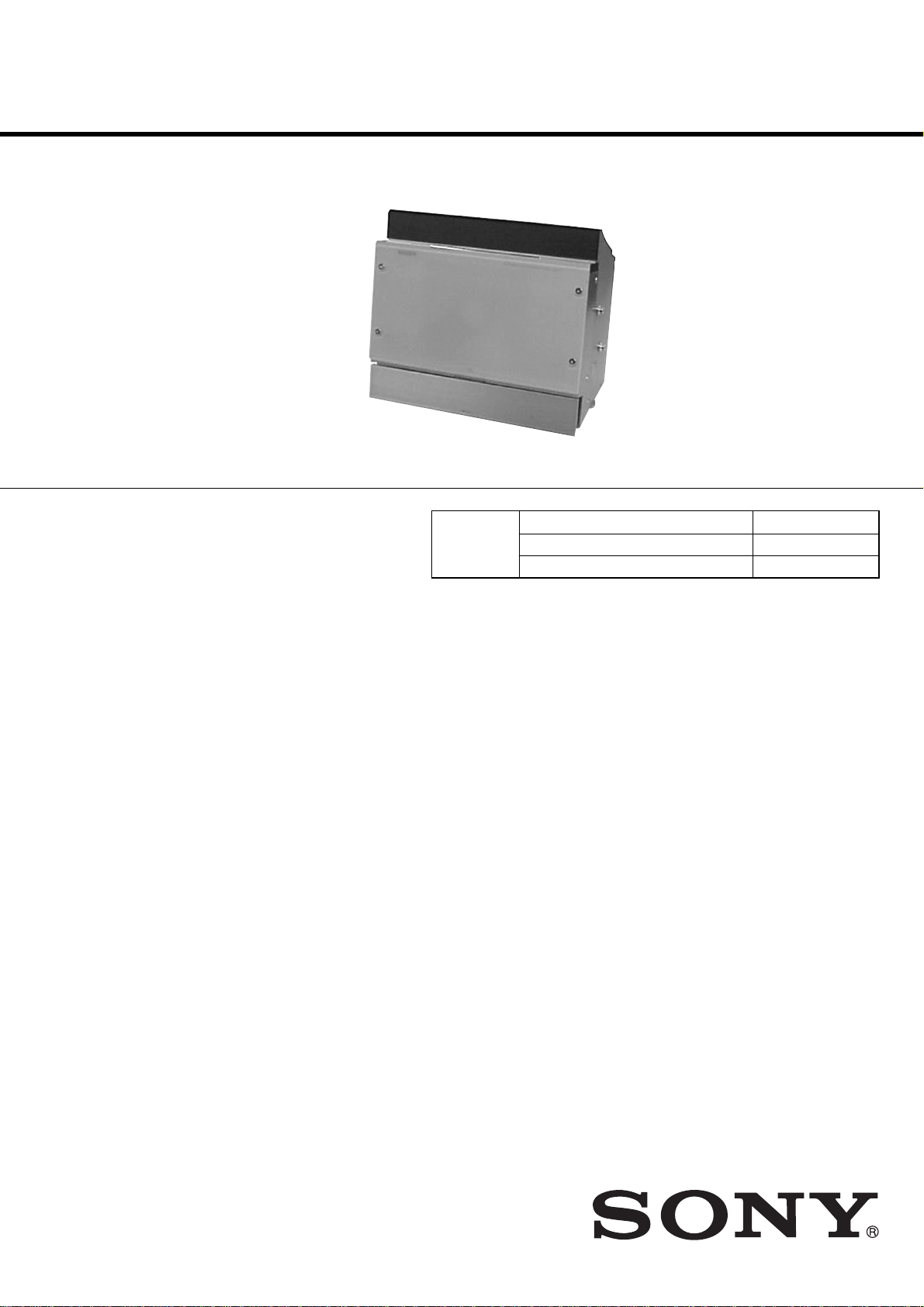
This set is the tuner, CD and amplifier
section in CMT-L1.
CD
SECTION
SPECIFICATIONS
Main unit (HCD-L1)
Amplifier section
For the U.S. model
AUDIO POWER SPECIFICATIONS
POWER OUTPUT AND TOTAL
HARMONIC DISTORTION:
With 4-ohm loads, both channels driven, from
120 - 10,000 Hz; rated 25 watts per channel
minimum RMS power, with no more than 10%
total harmonic distortion from 250 milliwatts to
rated output.
North American model:
Continuous RMS power output (reference):
European model:
DIN power output (rated): 20 + 20 W
Continuous RMS power output (reference):
Music power output (reference):
Other models:
The following measured at 220 V AC, 60 Hz
DIN power output (rated): 20 + 20 W
Continuous RMS power output (reference):
25 + 25 W
(4 ohms at 1 kHz, 10%
THD)
(4 ohms at 1 kHz, DIN)
25 + 25 W
(4 ohms at 1 kHz, 10%
THD)
25 + 25 W
(4 ohms at 1 kHz, DIN,
110 V - 240 V AC)
25 + 25 W
(4 ohms at 1 kHz, 10%
THD, 110 V - 240 V AC)
US Model
Canadian Model
AEP Model
UK Model
E Model
Model Name Using Similar Mechanism NEW
CD Mechanism Type CDM71A
Base Unit Type BU-31BD63A
Inputs
MD/TAPE IN (stereo minijack):
Outputs
MD/TAPE OUT (stereo minijack):
PHONES (stereo minijack):
DIGITAL CD OPTICAL OUT (Supported sampling
frequency: 44.1 kHz)
CD player section
System Compact disc and digital
Laser Semiconductor laser
Frequency response 2 Hz – 20 kHz
Tuner section
FM stereo, FM/AM superheterodyne tuner
FM tuner section
Tuning range
North American model: 87.5 - 108.0 MHz
Other models: 87.5 - 108.0 MHz
Antenna FM wire antenna
Antenna terminals 75 ohm unbalanced
Intermediate frequency 10.7 MHz
Sensitivity 450 mV (MD)/
250 mV (Tape),
impedance 47 kilohms
Sensitivity 250 mV,
impedance 1 kilohmes
Accepts headphones with
an impedance of 8 ohms
or more
audio system
(λ = 795 nm)
Emission
duration: continuous
(100-kHz step)
(50-kHz step)
— Continued on next page —
9-873-561-01
2002C1600-1
© 2002.03
MICRO Hi-Fi COMPONENT SYSTEM
Sony Corporation
Home Audio Company
Published by Sony Engineering Corporation
Page 2
HCD-L1
AM tuner section
Tuning range
North American model: 530 - 1,710 kHz
European model: 531 - 1,602 kHz
Other models: 530 - 1,710 kHz
Antenna AM loop antenna, external
Intermediate frequency 450 kHz
General
Power requirements
North American model: 120 V AC, 60 Hz
European model: 230 V AC, 50/60 Hz
Other models: 110 - 240 V AC ,
Power consumption
European model: See the nameplate
Other models: See the nameplate
Dimensions (w/h/d) Approx. 293 × 246 ×
Mass Approx. 3.5 kg
Design and specifications are subject to change
without notice.
(with the tuning interval
set at 10 kHz)
531 - 1,710 kHz
(with the tuning interval
set at 9 kHz)
(with the tuning interval
set at 9 kHz)
(with the tuning interval
set at 10 kHz)
531 - 1,602 kHz
(with the tuning interval
set at 9 kHz)
antenna terminal
50/60 Hz
0.2 W (at the Power
Saving Mode)
131 mm incl. projecting
parts and controls
SAFETY CHECK-OUT
After correcting the original service problem, perform the
following safety checks before releasing the set to the customer:
Check the antenna terminals, metal trim, “metallized” knobs, screws,
and all other exposed metal parts for A C leakage. Check leakage as
described below.
LEAKAGE
The A C leakage from any e xposed metal part to earth ground and
from all exposed metal parts to any exposed metal part having a
return to chassis, must not exceed 0.5 mA (500 microamperes).
Leakage current can be measured by any one of three methods.
1. A commercial leakage tester, such as the Simpson 229 or RCA
WT -540A. Follo w the manufacturers’ instructions to use these
instruments.
2. A battery-operated AC milliammeter. The Data Precision 245
digital multimeter is suitable for this job.
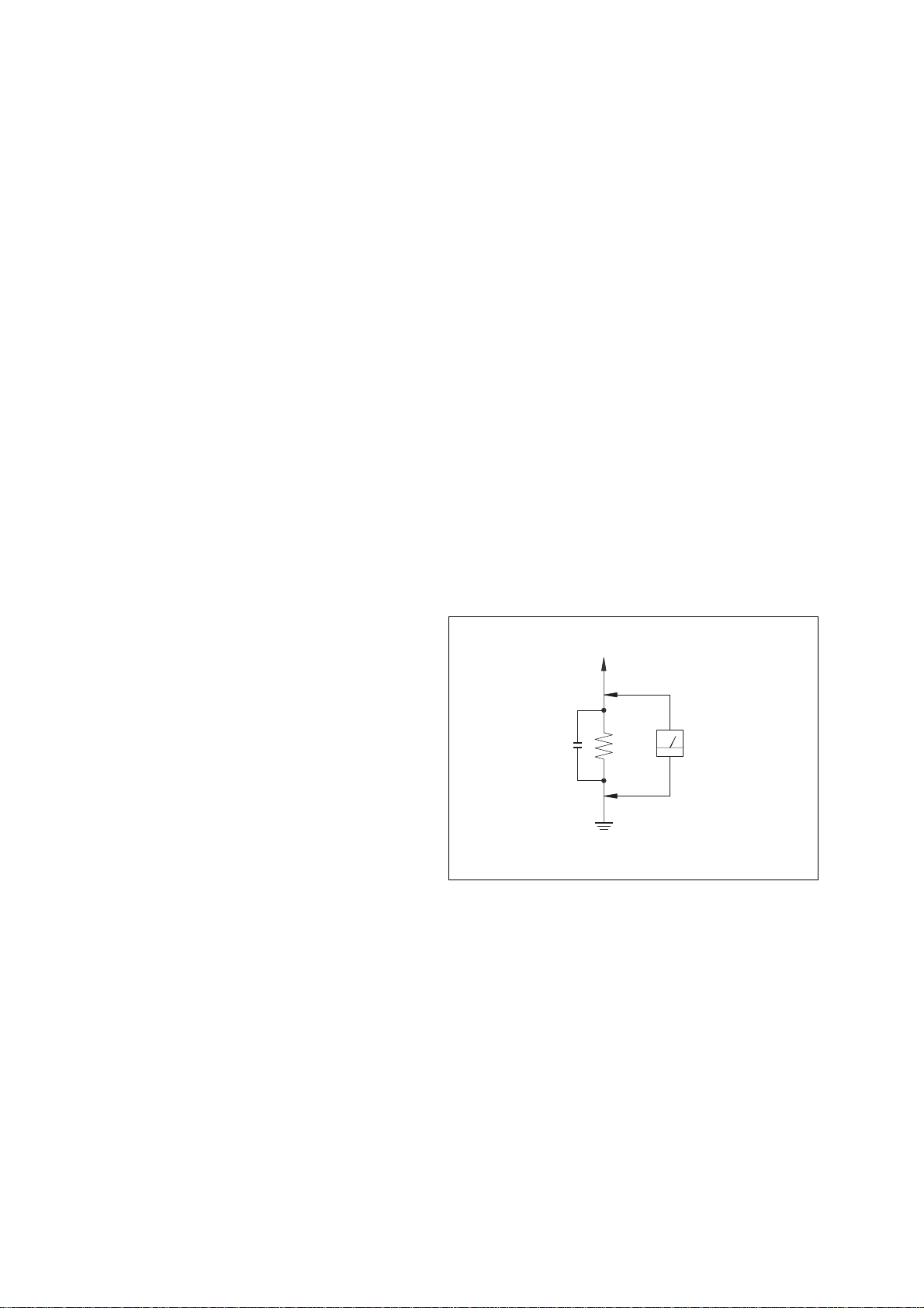
3. Measuring the voltage drop across a resistor by means of a
VOM or battery-operated A C voltmeter . The “limit” indication
is 0.75 V, so analog meters must have an accurate low-volta ge
scale. The Simpson 250 and Sanwa SH-63Trd are e xamples of
a passive VOM that is suitable. Nearly all battery operated
digital multimeters that have a 2V AC range are suitable. (See
Fig. A)
To Exposed Metal
Parts on Set
AC
0.15 µF
1.5 kΩ
Voltmeter
(0.75 V)
Earth Ground
Fig. A. Using an A C v oltmeter to check A C leakage.
2
Page 3

TABLE OF CONTENTS
HCD-L1
1. SERVICING NOTES ······················································· 4
2. GENERAL ·········································································· 5
3. DISASSEMBLY
3-1. Bottom Plate,Case ························································ 9
3-2. Front Panel Section ······················································ 9
3-3. POWER Board, AM/FM Tuner··································10
3-4. MAIN Board ······························································ 10
3-5. AMP Board, Regurator ··············································11
3-6. Door Panel, LED Board (R), Indicator ······················11
3-7. LED Board (L) ··························································· 12
3-8. FL (L1) Board ···························································· 12
3-9. SWITCH Board, TOUCH SWITCH Board··············· 13
3-10. CD Board ··································································· 13
3-11. CD-mechanism (CDM71A) ······································· 14
3-12. L.MOTOR Board ······················································· 14
3-13. ENCODER Board, D.sensor Board ··························· 15
3-14. RTL Pulley Assy ························································15
3-15. BD Board ··································································· 16
3-16. C.MOTOR Board, L.SENSOR Board ·······················16
3-17. Base Unit ···································································· 17
3-18. Holder Assy, Sled Motor Assy ··································· 17
3-19. RTR Pulley Assy ························································ 18
3-20. SPT Pulley Assy························································· 18
4. TEST MODE···································································· 19
6. DIAGRAMS
6-1. Block Diagrams CD Section ····································· 23
MAIN Section ···························································· 24
6-2. Circuit Boards Location ············································· 25
6-3. Printed Wiring Board BD Section (Side A) ·············· 26
6-4. Printed Wiring Board BD Section (Side B) ·············· 27
6-5. Schematic Diagram BD Section ······························· 28
6-6. Schematic Diagram CD Section ······························· 29
6-7. Printed Wiring Board CD Section (Side A) ·············· 30
6-8. Printed Wiring Board CD Section (Side B) ·············· 31
6-9. Printed Wiring Board MOTOR Section ····················32
6-10. Schematic Diagram MOTOR Section······················· 33
6-11. Printed Wiring Board MAIN Section (Side A) ········· 34
6-12. Printed Wiring Board MAIN Section (Side B) ········· 35
6-13. Schematic Diagram MAIN Section (1/2)·················· 36
6-14. Schematic Diagram MAIN Section (2/2)·················· 37
6-15. Printed Wiring Board AMP Section (Side A) ··········· 38
6-16. Printed Wiring Board AMP Section (Side B) ···········39
6-17. Schematic Diagram AMP Section·····························40
6-18. IC Block Diagrams····················································· 41
6-19. Printed Wiring Board DISPLAY Section ·················· 42
6-20. Schematic Diagram DISPLAY Section····················· 43
6-21. Printed Wiring Board SWTICH Section ··················· 44
6-22. Schematic Diagram SWTICH Section······················ 45
6-23. Printed Wiring Board POWER Section ···················· 46
6-24. Schematic Diagram POWER Section ······················· 47
6-25. IC PIN FUNCTION DESCRIPTION ························ 48
5. ELECTRICAL ADJUSTMENTS ······························· 22
7. EXPLODED VIEWS
7-1. Case Section ······························································· 51
7-2. Chassis Section ·························································· 52
7-3. Front Panel Section ···················································· 53
7-4. Mechanism Section(CDM71A)-1 ······························ 54
7-5. Mechanism Section(CDM71A)-2 ······························ 55
7-6. Base Unit Section (BU-31BD63A) ···························· 56
8. ELECTRICAL PARTS LIST······································· 57
3
Page 4
HCD-L1
SECTION 1
SERVICING NOTES
NOTES ON HANDLING THE OPTICAL PICK-UP
BLOCK OR BASE UNIT
The laser diode in the optical pick-up block may suffer electrostatic
break-down because of the potential difference generated by the
charged electrostatic load, etc. on clothing and the human body.
During repair, pay attention to electrostatic break-down and also
use the procedure in the printed matter which is included in the
repair parts.
The flexible board is easily damaged and should be handled with
care.
NOTES ON LASER DIODE EMISSION CHECK
The laser beam on this model is concentrated so as to be focused on
the disc reflective surface by the objective lens in the optical pickup block. Therefore, when checking the laser diode emission,
observe from more than 30 cm away from the objective lens.
Laser component in this product is capable
of emitting radiation exceeding the limit for
Class 1.
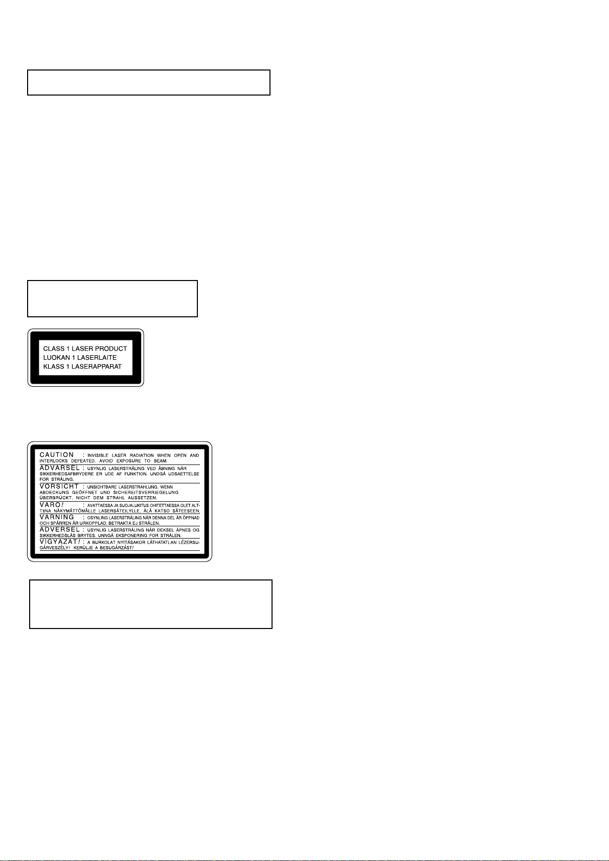
This appliance is classified as a CLASS 1 LASER product. The
CLASS 1 LASER PRODUCT MARKING is located on the rear
exterior.
Notes on chip component replacement
•Never reuse a disconnected chip component.
• Notice that the minus side of a tantalum capacitor may be
damaged by heat.
Flexible Circuit Board Repairing
•Keep the temperature of soldering iron around 270˚C
during repairing.
• Do not touch the soldering iron on the same conductor of the
circuit board (within 3 times).
• Be careful not to apply force on the conductor when soldering
or unsoldering.
ATTENTION AU COMPOSANT AYANT RAPPORT
À LA SÉCURITÉ!
LES COMPOSANTS IDENTIFÉS P AR UNE MARQUE 0 SUR LES
DIAGRAMMES SCHÉMA TIQUES ET LA LISTE DES PIÈCES SONT
CRITIQUES POUR LA SÉCURITÉ DE FONCTIONNEMENT. NE
REMPLACER CES COMPOSANTS QUE PAR DES PIÈSES SONY
DONT LES NUMÉROS SONT DONNÉS DANS CE MANUEL OU
DANS LES SUPPÉMENTS PUBLIÉS PAR SONY.
SAFETY-RELATED COMPONENT WARNING!!
COMPONENTS IDENTIFIED BY MARK 0 OR DOTTED LINE WITH
MARK 0 ON THE SCHEMATIC DIAGRAMS AND IN THE PARTS
LIST ARE CRITICAL TO SAFE OPERATION. REPLACE THESE
COMPONENTS WITH SONY PARTS WHOSE PART NUMBERS
APPEAR AS SHOWN IN THIS MANUAL OR IN SUPPLEMENTS
PUBLISHED BY SONY.
This caution
label is
located inside
the unit.
CAUTION
Use of controls or adjustments or performance of procedures
other than those specified herein may result in hazardous radiation
exposure.
4
Page 5
SECTION 2
GENERAL
List of Button Locations and Reference Pages
HCD-L1
This section is extracted
from instruction manual.
How to use this page
Use this page to find the location of buttons and other
parts of the system that are mentioned in the text.
Main unit
ALPHABETICAL ORDER
A – F
CD cover 2 (11)
CD u 7 (11 - 13)
CD x 8 (11, 12)
DISPLAY 6 (17, 20, 21)
Display 1 (20, 21)
FUNCTION qa (11 - 14, 16, 23,
25)
P – Z
PHONES jack qf
PLAY MODE/TUNING MODE
qd (11 - 16, 25)
Remote sensor qg
TUNER/BAND 9 (15, 16, 25)
TUNING +/– qs (15, 16)
VOL +/– (19)
q;
12 3
Illustration number
PLAY MODE qg (9, 13, 14)
Name of button/part Reference page
RR
BUTTON DESCRIPTIONS
/1? (power) 4 (8, 19)
./> qs (11 - 13)
m/M qs (11)
Z 3 (11)
V OPEN 5
To open the front cover, push
down on V OPEN.
qg
qf
5
6789
qs
4
q;qaqd
5
Page 6
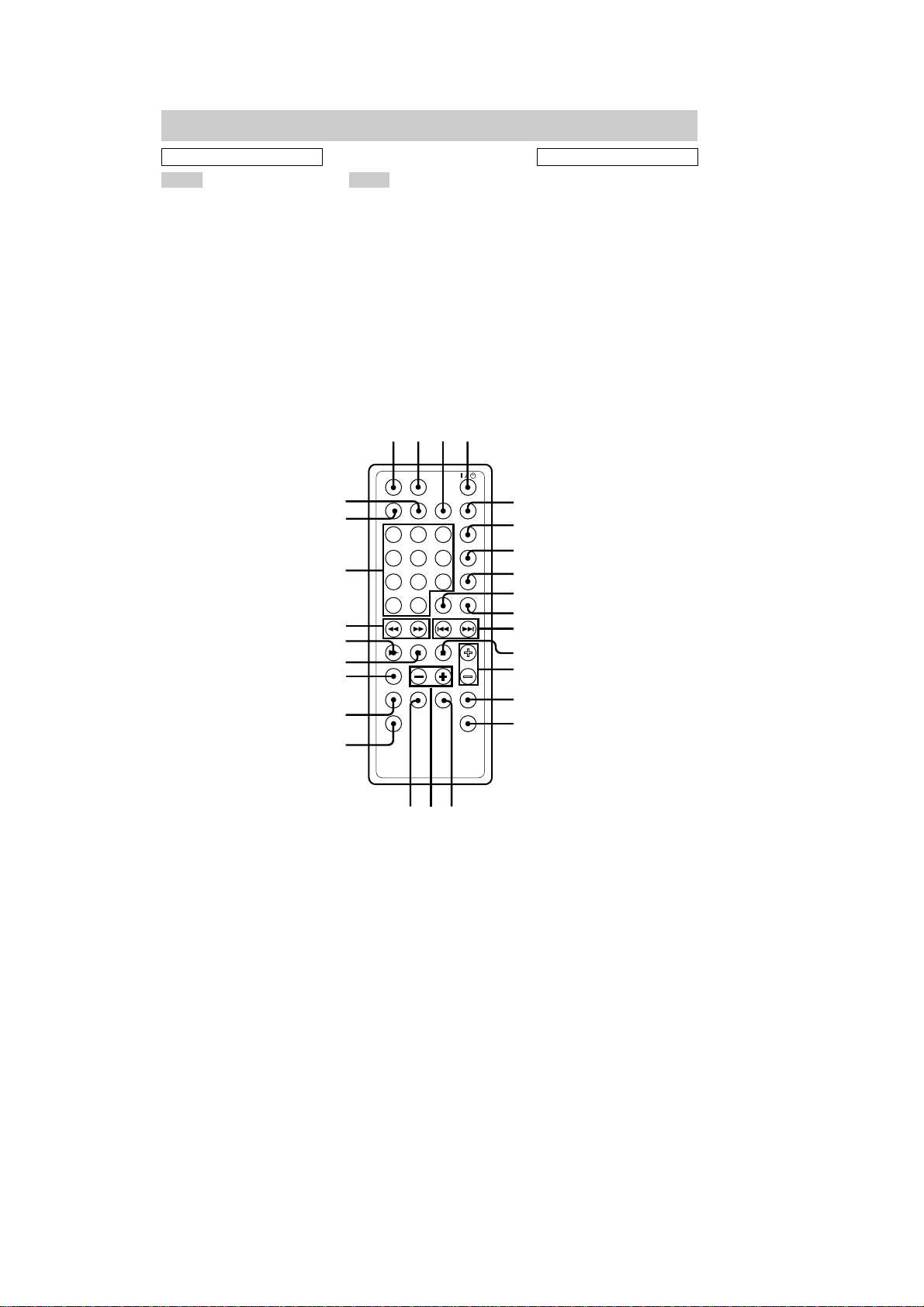
HCD-L1
Remote control
ALPHABETICAL ORDER
A – F
CD N wd (11 - 13)
CD X ws (11)
CD x qs (11, 12)
CLEAR 9 (12, 13, 17)
CLOCK/TIMER SELECT 6
(19)
CLOCK/TIMER SET 7 (10, 19)
CURSOR T/t wf (10, 13)
DIMMER ql (20)
DISPLAY wh (17, 20, 21)
DSG qf (18)
ENTER/YES 8 (10, 12 - 15, 17,
19, 23)
FM MODE qh (16)
FUNCTION w; (11 - 14, 16, 23)
L – Z
Letter/Numeric buttons wg (12,
13, 16)
MENU/NO q; (13 - 17, 23)
NAME EDIT/SELECT 3 (13,
17)
PLAY MODE/TUNING MODE
qk (11 - 16)
PRESET EQ qg (18)
REPEAT qh (11)
SCROLL 5 (14, 21)
SLEEP 2 (18)
TIME wj (12, 20, 21)
TUNER BAND wa (15, 16)
TUNING +/– qj (15, 16)
VOL +/– qd (19)
1 234
wj
wh
wg
wf
wd
ws
wa
w;
ql
BUTTON DESCRIPTIONS
@/1 (power) 4 (8, 19)
./> qa (10 - 14, 19)
m/M wf (11)
Z 1 (11)
5
6
7
8
9
0
qa
qs
qd
qf
qg
qhqjqk
6
Page 7
HCD-L1
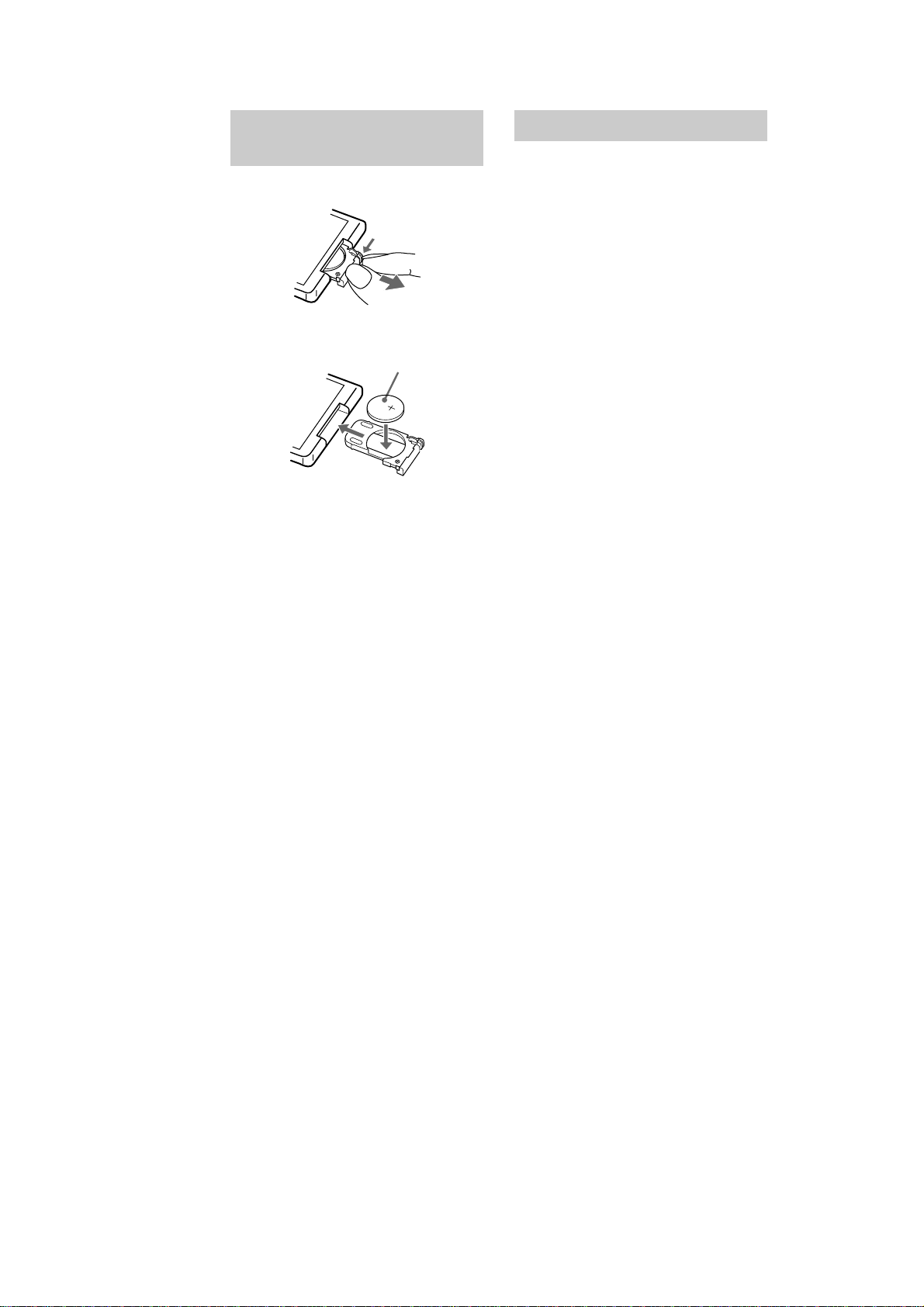
Replacing the battery in
the remote
1
Slide out and remove the battery case.
2
Insert a new lithium battery CR2025
with the + side facing up.
a lithium battery CR2025
3
Slide the battery case back in.
Tip
When the battery no longer operates the remote,
replace the battery with a new one.
Note
If you are not going to use the remote for a long time,
remove the battery to avoid damage caused by
corrosion from battery leakage.
Notes on lithium battery
•Keep the lithium battery out of the reach of
children.
Should the battery be swallowed, immediately
consult a doctor.
•Wipe the battery with a dry cloth to assure a good
contact.
• Be sure to observe the correct polarity when
installing the battery.
• Do not hold the battery with metallic tweezers,
otherwise a short-circuit may occur.
WARNING
Battery may explode if you mistreated.
Do not recharge, disassemble or dispose of in fire.
Setting the clock
1
Turn on the system.
2
Press CLOCK/TIMER SET on the
remote.
3
Press . or > on the remote
repeatedly to set the day, and then
press ENTER/YES or CURSORt on
the remote.
The hour indication flashes.
4
Press . or > on the remote
repeatedly to set the hour, and then
press ENTER/YES or CURSORt on
the remote.
The minute indication flashes.
5
Press . or > on the remote
repeatedly to set the minute, and then
press ENTER/YES on the remote.
If you make a mistake
Press TCURSOR or CURSORt on the
remote repeatedly until the indication you want
to change (day, hour, minute) flashes, and then
change the setting.
To adjust the clock
1
Press CLOCK/TIMER SET on the remote.
2
Press . or > on the remote repeatedly
until “CLOCK SET?” appears in the display,
and then press ENTER/YES on the remote.
3
Do the same procedures as steps 3 to 5
above.
7
Page 8
HCD-L1
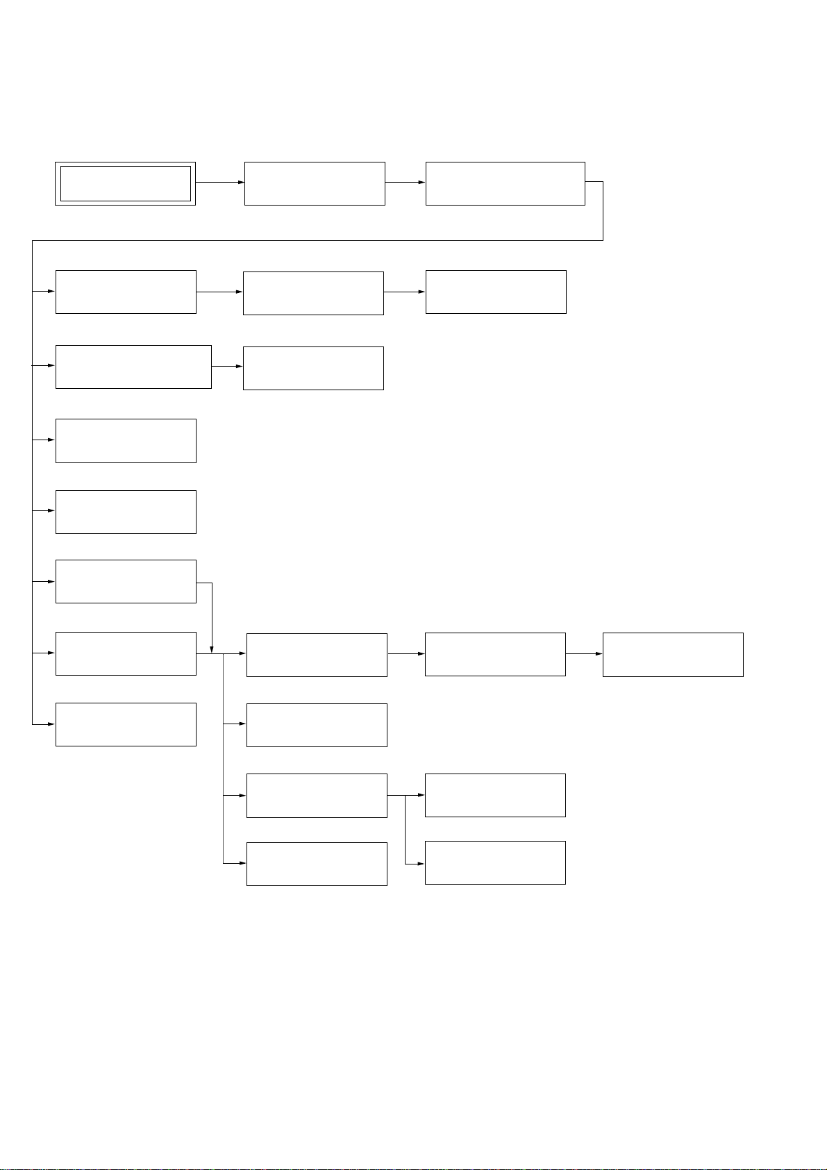
SECTION 3
DISASSEMBLY
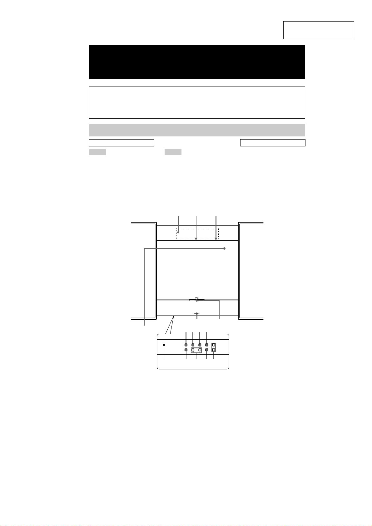
• The equipment can be removed using the following procedure.
SET (HCD-L1)
POWER BOARD,
AM/FM Tuner
(Page 10)
DOOR PANEL,
LED BOARD (R),INDICATOR
TOUCH SWITCH BOARD
(Page 11)
FL(L1)
BOARD
(Page 12)
SWITCH BOARD,
(Page 13)
BOARD
CD
(Page 13)
BOTTOM PLATE,CASE
(Page 9)
MAIN BOARD
(Page 10)
LED BOARD (L)
(Page 12)
FRONT PANEL SECTION
(Page 9)
AMP BOARD,
REGURATOR
(Page 11)
CD-MECHANISM
(CDM71A)
(Page 14)
BOARD
BD
(Page 16)
L.MOTOR BOARD
(Page 14)
C MOTOR BOARD,
L.SENSOR BOARD
(Page 16)
BASE UNIT
(BU-31BD63A)
(Page 17)
SPT PULLEY ASSY
(Page 18)
ENCODER BOARD,
D.SENSOR BOARD
(Page 15)
HOLDER ASSY,
SLED MOTOR ASSY
(Page 17)
RTR PULLEY ASSY
(Page 18)
RTL PULLEY ASSY
(Page 15)
8
Page 9
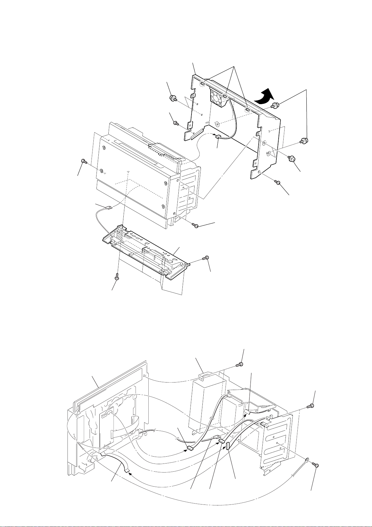
Note : Follow the disassembly procedure in the numerical order given.
)
3-1. Bottom Plate,Case
qa
t
wo screws
× 6
(+PTT 3
)
7
s
crew (+PTT 3
6
t
wo screws (SS)
× 6
qg
case
)
qd
c
onnector
qf
(CN801)
three
claws
qs
5
f
our screws (SS)
8
t
HCD-L1
wo screws (SS)
3
earth plate
1
five screws (+BVTP 3
3-2. Front Panel Section
qa
Front panel section
× 8
9
s
crew (+PTT 3
q;
t
wo screws (+PTT 3
4
b
ottom plate
2
three screws (+BVTP 2.6
)
4
5
c
hassis section
× 6
)
×
8)
two screws (+BVTP 2.6
6
flat type wire (13 core)
×
8)
× 6
)
7
f
lat type wire (11 core)
q;
c
onnector
(CN1321)
1
earth plate
9
c
onnector (CN1201)
8
c
onnector (CN401)
3
two
screws (+BVTP 2.6
2
screw (+BVTP 3
×
×
8)
8
9
Page 10
HCD-L1
s
3-3. POWER Board, AM/FM Tuner
1
7
AM/FM t
uner
6
flat type wire
(11core or 15core)
connector (CN800)
2
two
screws
(+BVTP 3
3
×
8)
4
POWER board
connector (CN500)
3-4. MAIN Board
1
flat type wire (23core)
2
three
(+BVTP 3
screws
×
5
two
screws
(+BVTP 3
8)
5
MAIN board
×
8)
3
two
claw
10
4
Page 11
3-5. AMP Board, Regurator
r
qs
qg
screw
(+BVTP 3
×
8)
qh
regurator
qd
two
screws
(+BVTP 3
×
8)
qf
screw
(+BVTP 3
5
four
screws
(+BVTP 3
×
3
8)
q;
(+BVTP 3
×
8)
four
screws
×
8)
1
connector (CN300)
qa
connector
7
6
two
2
two
screws
(+BVTP 3
8
shield case (SM-bottom)
×
8)
HCD-L1
claws
4
shield case (SM-top)
3-6. Door Panel, LED Board (R), Indicator
4
sheet (CD)
2
two screws
(panel)
3
ornamental plate (CD)
8
indicator (BS)
9
AMP board
1
two screws
(panel)
6
s
crew (+BTP 2.6
×
6)
7
holder (LED-R)
q;
LED board (R)
9
two
screws (+BVTP 2.6
5
connecto
(CN1303)
×
8)
11
Page 12
HCD-L1
)
3-7. LED Board (L)
4
two
5
LED board (L)
screws (+BVTP 2.6
1
connector (CN1302)
2
screw (+BTP 2.6
×
8)
3
holder (LED-L)
×
6)
3-8. FL (L1) Board
2
FL(L1) board
1
two
screws (+BVTP 2.6
×
8
12
Page 13
3-9. SWITCH Board, TOUCH SWITCH Board
d
)
3
TOUCH SWITCH board
2
two
screws
(+BVTP 2.6
×
8)
1
c
onnector (CN1302)
6
SWITCH boar
HCD-L1
3-10. CD Board
4
c
onnector (CN1303)
2
(CN751)
c
onnector
6
bracket (CD-MT)
5
two screws (+BVTP 3
5
f
ive screws
(+BVTP 2.6
4
CD board
×
8)
×
8)
1
three screws
(+BVTP 2.6
×
8
3
c
onnector
(CN752)
13
Page 14
HCD-L1
)
3-11. CD-Mechanism (CDM71A)
4
blacket
5
CD mechanism (CDM71A)
1
two
screws
(+BVTP 2.6
×
8
3
six
screws (+BVTP 2.6
3-12. L.MOTOR Board
1
belt (CDM71 )
×
2
two
screws
(+BVTP 2.6
8)
3
Remove solder (two portions ).
motor (LD) assy
(M711)
×
8)
4
(+BTP M 2.6
5
L.MOTOR board
two screws
×
6)
14
2
belt (roller )(L)
Page 15
3-13. ENCODER Board, D.SENSOR Board
4
D.SENSOR board
3
screw
(+BTP M 2.6
1
2
ENCODER
×
6)
screw (+PWH,2X6)
board
HCD-L1
3-14. RTL Pulley Assy
3
RTL pulley assy
Disengage the claw and rotate the RTL pulley assy in the direction of , and
remove your hands at the position where the shaft agrees with the hole shape on the
chassis.
RTL pulley assy
2
1
claw
2
15
Page 16
HCD-L1
w
)
3-15. BD Board
5
h
ook
(RED)
1
Remove solder (two portions ).
(BLK)
6
BD board
3
scre
3-16. C MOTOR Board, L.SENSOR Board
4
Connector
(CN711)
1
belt (CDM71 )
4
flxible
8
Connector
(CN753)
9
(CN755)
board
7
Connector
(CN754)
Connector
q;
(+BTP M 2.6
2
Remove solder (two portions ).
2
Remove solder
(two portions ).
5
C.MOTOR board
6
motor (CK) assy
(M701)
screw
×
6)
3
two screws
(+BTP M 2.6
×
6
16
qa
L.SENSOR board (R)
Page 17
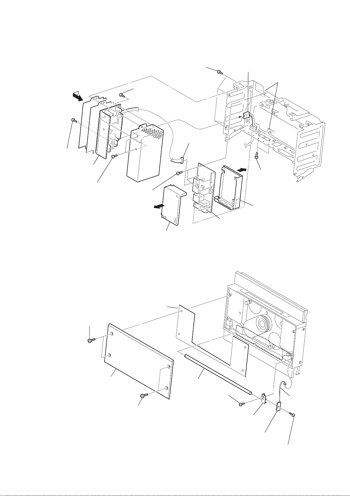
3-17. Base Unit (BU-31BD63A)
Rotate the SPT pulley assy in the direction of to move the Base unit shaft
forward.
1
1
cam
HCD-L1
2
screw
(+PTPWH M2.6)
5
base unit
(BU-31BD)
SPT pulley assy
shaft
3-18. Holder Assy, Sled Motor Assy
9
two screws
(+PTPWH M2.6)
q;
h
ook
shaft
8
screw
(+PTPWH M2.6)
qa
base unit
4
flxible
board
qd
sled motor assy
4
3
holder assy
7
tension coil spring (holder)
5
BD board
qs
screw
(+P 2
×
3)
6
tension coil spring (holder)
1
Remove solder
(two portions ).
(RED)
(BLK)
2
Remove solder
3
screw
(+BTP 2
× 8
)
(two portions ).
17
Page 18
HCD-L1
3-19. RTR Pulley Assy
3
RTR pulley assy
Disengage the claw and rotate the RTR pulley assy in the direction of , and
remove your hands at the position where the shaft agrees with the hole shape on the
chassis.
RTR pulley assy
2
1
claw
2
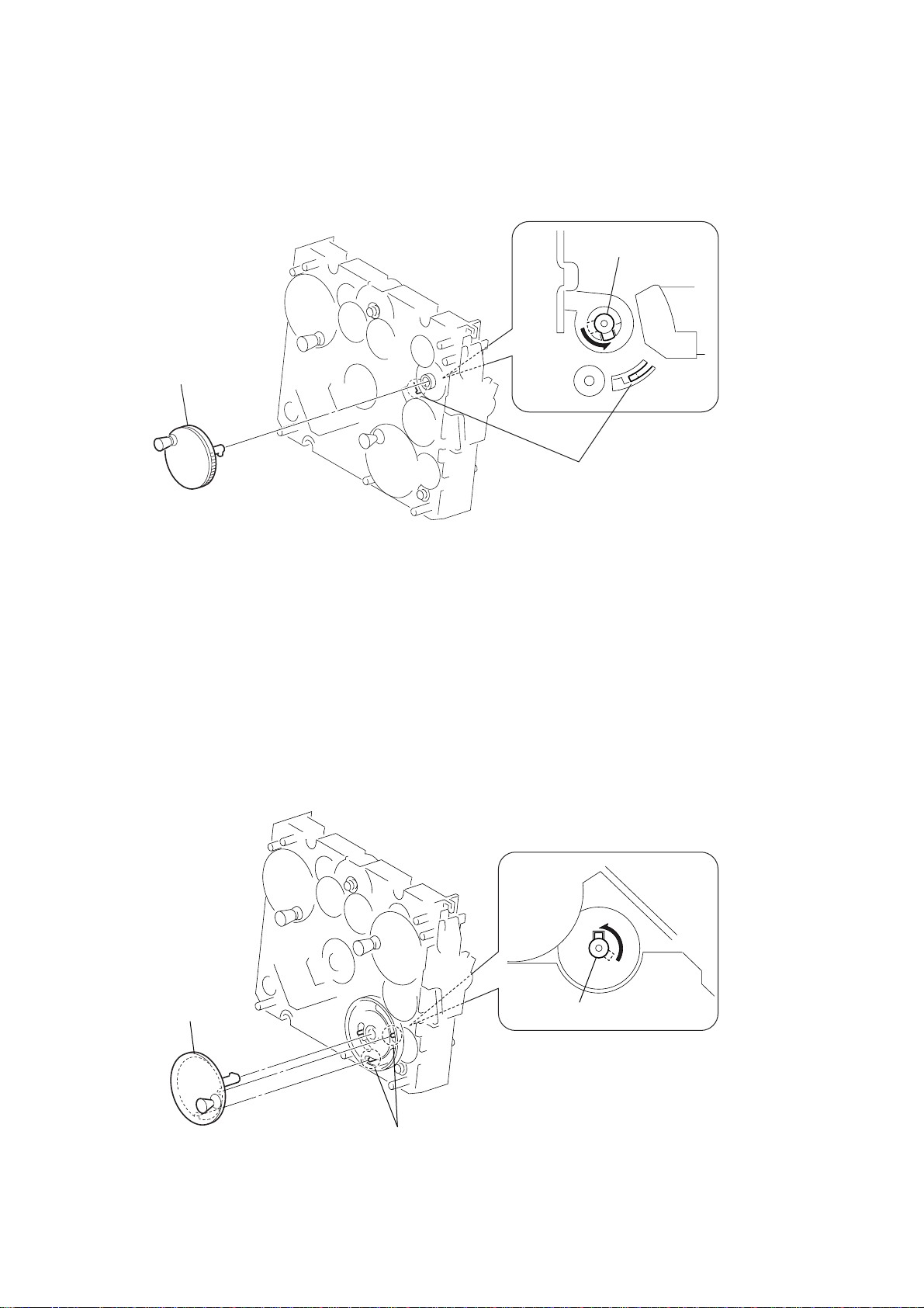
3-20. SPT Pulley Assy
2
SPT pulley assy
Rotate the SPT pulley assy in the direction of , and remove your hands
at the position where the shaft agrees with the hole shape on the chassis.
SPT pulley assy
1
1
18
When installing, align the protruded portion of the KT gear with groove of the SPT
pulley assy.
Page 19
SECTION 4
TEST MODE
HCD-L1
[Key Check Mode]
* Keyboard check.
Procedure:
1. Press the ?/1 button to turn the set ON.
2. To enter the test mode, press three buttons DISPLAY , NX
and > simultaneously.
3. In the key check mode, the fluorescent indicator displays
“KEY00”. Each time a button is pressed, “KEY00” value
increases. However, once a button is pressed, it is no longer
taken into account.
4. To exit from this mode, press three buttons DISPLAY , NX
and > simultaneously.
[Version Display Mode]
* The version or destination is displayed.
Procedure:
1. Press the ?/1 button to turn the set ON.
2. To enter the test mode, press three buttons DISPLAY , VOL+
and VOL– simultaneously.
3. The model name and destination are displayed.
4. Press the DISPLAY button. The STR version is displayed.
5. Press the DISPLAY button again. The CD version is displayed.
6. Press the DISPLAY button. The model name and destination
are displayed again.
7. To exit from this mode, press the ?/1 button to turn off the set.
[FL T ube Test Mode]
* All fluorescent segments are tested.
Procedure:
1. Press the ?/1 button to turn the set ON.
2. To enter the test mode, press three buttons DISPLAY , NX
and VOL– simultaneously.
3. All segments are turned on.
PROGRAM REP TEXT TRACK TUNED MONO1 DISC STEREO AUTO PRESET DSGSHUFFLE
DAILY
c
SLEEP
[Amp Test Mode]
* Combinatin of preset equalizer and volume is changed for the
amplifier test.
Procedure:
1. Press the ?/1 button to turn the set ON.
2. To enter the test mode, press three buttons . , NX and
> simultaneously.
3. The message “7[TESTMIN]” appears.
4. Press the DISPLAY and NX buttons simultaneously.
5. The message “8[TESTMID]” appears.
6. The messages “9[TESTMAX]”, “10[TESTSUR]”, “7[TESTMIN]”,
, , are changed by every pressing of the DISPLAY and NX
buttons simultaneously.
7. Volume le vel is changeable at three steps as “V OLUME MIN”,
“VOLUME 21”, “VOLUME MAX” by pressing VOL+ or
VOL– button.
8. In this test mode, the tuning mode is set to the preset mode.
9. T o exit from this mode, press the ?/1 button to tur n off the set.
[Forced Reset]
* All micro-processors are forced to reset at the same time.
Procedure:
1. Press the ?/1 button to turn the set ON.
2. Press three buttons DISPLAY , TUNER/BAND and
FUNCTION simultaneously.
3. The fluorescent indicator tube displays the message “COLD
RESET” and the set is reset. Then the set is turned off.
[CD Ship Position]
Procedure:
1. Press the ?/1 button to turn the set ON.
2. Press the FUNCTION button for the setting CD.
3. Press three buttons . , V OL+ and V OL– simultaneously .
4. The fluorescent indicator tube displays the message
“ST ANDBY” and CD is set to the shipment position. Then the
set is turned off.
4. Press the DISPLAY button. All segments are turned off.
5. Press the DISPLAY button. Conf irm the pattern of se gments.
DAILY
REP TEXT TRACK STEREO AUTO DSGSHUFFLE
6. Press the DISPLAY button. Conf irm the pattern of se gments.
PROGRAM TUNED MONO1 DISC PRESET
c
SLEEP
7. Every pressing of the DISPLAY b utton turns on each segment
one after another in the same order.
8. T o exit from this mode, press the ?/1 button to turn off the set.
[Aging Mode]
Procedure:
1. Press the ?/1 button to turn the set ON.
2. Insert the disc.
3. Select the FUNCTION to CD.
4. To enter the test mode, press three buttons . , TUNER/BAND
and Z OPEN simultaneously .
5. Aging operation starts automatically.
6. The CD cover opens ,closes and the first track is played. Then
the last track is played.
7. The CD cover opens again, and the message “A GIN00000001”
is displayed. This value is cycle times of aging operation and
displays hexadecimal data.
8. The cover closes and aging operation is continued.
9. To exit from this mode, press the ?/1 button to turn off the set.
19
Page 20
HCD-L1
[Error History Display Mode]
Procedure:
Setting Method of Test Mode
1. Press the ?/1 button to turn the set ON.
2. Select the FUNCTION to CD.
3. To enter the test mode, press three buttons . , V OL+ and
> simultaneously.
4. Confirm to display “dvt ERR CODE”.
5. Press the Z OPEN button.
Releasing Method of Test Mode
1. Press the x button to display “dvt ERR CODE”.
2. Press the x button.
Menu Selection of Error History Display Mode
1. Select the operation in the menu by pressing the . or >
button.
2. Press the Z OPEN button. The menu is selected. If returning
to the menu again, press the x button.
DISPLAY OF TIMES OF ERROR
DISPLAY OF MECHANISM ERROR HISTORY
RESET OF MECHANISM ERROR HISTORY
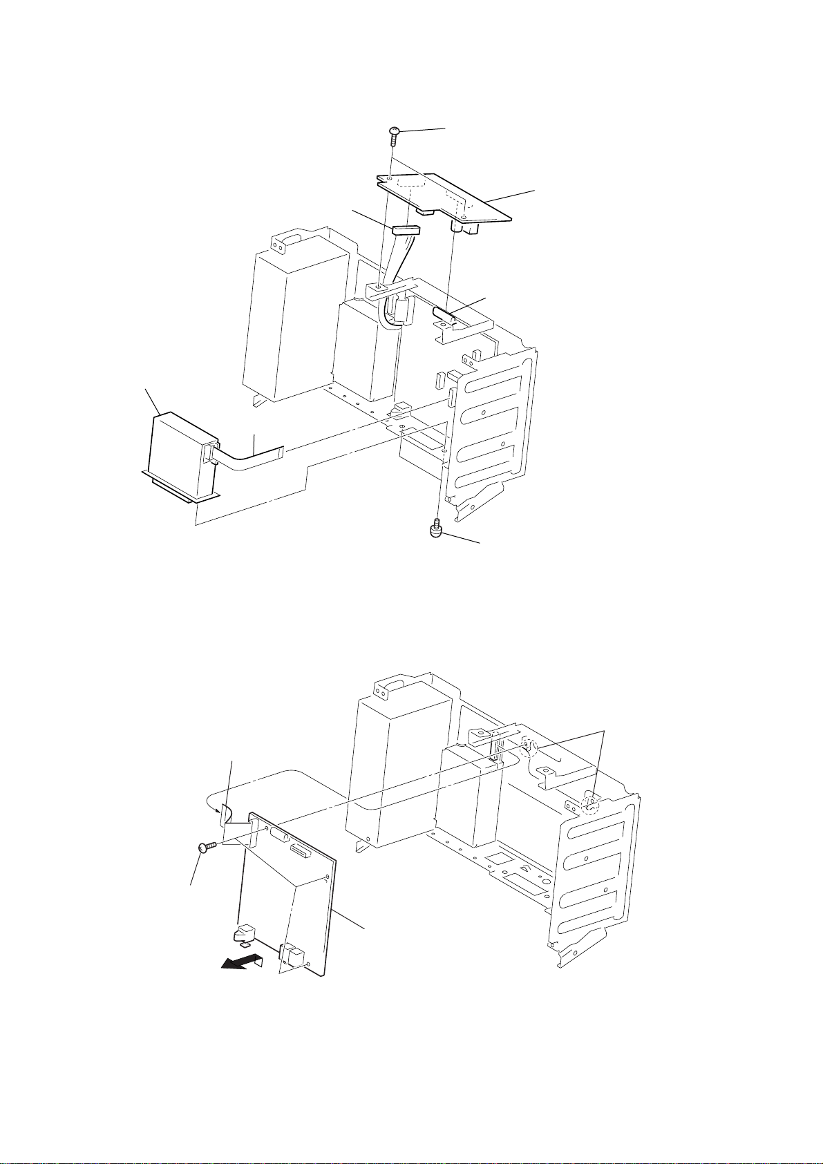
RESET OF ERROR HISTORY
RESET OF NO DISC ERROR HISTORY
DISPLAY OF NO DISC ERROR HISTORY
" Emc=**Edc=## "
" dvt ECODE MEC "
" dvt ECNT0 MEC "
" dvt ECNT0 ALL "
" dvt ECNT0 BU "
" dvt ECODE BU "
Display of Times of Error
* Number of times of mechanism error and no disc error is displayed
in hexadecimal.
DISPLAY : “ Emc=**Edc=## “
** : number of times of mechanism error (hexadecimal)
## : number of times of no disc error (hexadecimal)
Display of Mechanism Error History
1. Select the operation in the menu by pressing the . or >
button to display “dvt ECODE MEC”.
2. Press the Z OPEN button.
3. Select the mechanism error code by pressing the . or >
button.
DISPLAY : “ E**M##%%0000 “
** : order of mechanism error happens (hexadecimal)
00 : the newest error
09 : the error ten times before
## : completion of an initialization (hexadecimal)
ff : completion
others : not completed
%% : condition of CDM operation when the trouble happened
(hexadecimal)
00 : during an initialization
1x : during opening (x : not fixed)
16 to 19 : during a kick by falure of opening
2x : completion of opening
28 : completion of opening under the condition of no disc
3x : during close request
4x : during open request
5x : during closing
6x : during chucking
80 : during releasing
9x : during operation of BU down
ax : during operation of shutter opening or closing
b0 : during BU up request
c0 : during BU down request
dx : during operation of BU up
0000: fixed
Reset of Mechanism Error History
1. Select the operation in the menu by pressing the . or >
button to display “dvt ECONT0 MEC”.
2. Press the CD PLAY button. Mechanism error history is reset.
Display of No Disc Error History
1. Select the operation in the menu by pressing the . or >
button to display “dvt ECODE BU”.
2. Press the Z OPEN button.
3. Select the no disc code by pressing the . or > button.
DISPLAY : “ E**D##%%@@&& “
** : order of no disc happens (hexadecimal)
00 : the newest
09 : ten times before
## : description of the trouble (hexadecimal)
01 : focus NG
02 : GFS NG
03 : time-over of starting
04 : continuous unlock of focus
05 : no input of Q-codes in fixed time
%% : condition when the trouble happened (hexadecimal)
01 : during shipment position processing
02 : during power off processing
03 : during processing of initialization
04 : during stop condition
05 : during stop processing
06 : during process of starting
07 : during process of TOC reading
08 : during search operation
09 : during playback
0a : during pause
0b : during playback manual searching
0c : during pause manual searching
@@ : do not care
&& : rotating speed of a disc when the trouble happened
(hexadecimal)
01 : x1
02 : x2 (double speed)
03 : x4
20
Page 21
Reset of No Disc Error History
1. Select the operation in the menu by pressing the . or >
button to display “dvt ECONT0 BU”.
2. Press the CD PLAY button. No disc error history is reset.
Reset of Error History
1. Select the operation in the menu by pressing the . or >
button to display “dvt ECONT0 ALL”.
2. Press the CD PLAY button. Error history is reset.
[Servo T est Mode]
*Error Rate Display
Procedure:
Setting Method of Test Mode
1. Press the ?/1 button to turn the set ON.
2. Insert the disc.
3. Select the FUNCTION to CD.
4. Press the NX button to play the CD.
5. To enter the test mode, press three buttons DISPLAY , VOL+
and FUNCTION simultaneously.
6. Press the . or > button to display “dvt ERR RATE”.
7. Press the Z OPEN button.
HCD-L1
Description of Error Rate
" ****####%%@@&& "
C1 C2 TNO MIN SEC
Releasing Method of Test Mode
1. Press the x button to display “dvt ERR RATE”.
2. Press three buttons DISPLAY , VOL+ and FUNCTION
simultaneously.
21
Page 22

HCD-L1
)
SECTION 5
ELECTRICAL ADJUSTMENTS
CD SECTION
Note :
1. CD Block is basically designed to operate without adjustment.
Therefore, check each item in order given.
2. Use YEDS-18 disc (3-702-101-01) unless otherwise indica ted.
3. Use an oscilloscope with more than 10MΩ impedance.
4. Clean the object lens by an applicator with neutral detergent
when the signal level is low than specified value with the
following checks.
RF Level Check
oscilloscope
BD board
TP(RFAC)
TP(DVC)
Procedure :
1. Connect oscilloscope to TP (RFAC).
2. Turned Power switch on.
3. Load a disc (YEDS-18) and playback the number five track.
4. Confirm that oscilloscope waveform is clear and check RF signal
level is correct or not.
Note: Clear RF signal waveform means that the shape “◊” can be
clearly distinguished at the center of the waveform.
Adjustment Location :
[ BD (CD) BOARD ] — SIDE A —
IC103
RF signal waveform
VOLT/DIV : 200mV
TIME/DIV : 500ns
level : 1.1 ± 0.3Vp-p
E-F Balance (1 Track jump) Check
oscilloscope
BD board
TP (TE)
TP (DVC)
+
–
Procedure:
1. Connect oscilloscope to TP (TE) and TP (DVC) board.
2. Turned Power switch on.
3. Load a disc (YEDS-18) and playback the number five track.
4. Press the u button. (Becomes the 1track jump mode.)
5. Confirm that the level B and A (DC v oltage) on the oscilloscope
waveform.
1 track jump waveform
Center of
waveform
IC101
TP(DVC)
TP(TE)
TP
(RFAC)
B
0V
level=1.3 ±0.6Vp-p
Specification level: x 100=less than ±22%
A
B
Symmetry
22
A (DC voltage
Page 23

6-1. Block Diagrams CD Section
HCD-L1
SECTION 6
DIAGRAMS
OPTICAL PICK-UP
BLOCK
5
VCC
8
PD1
4
PD2
10
I5-10
8
I1-6
6
LD+
11
GND
7
2
S1
LIMIT IN
SWITCH
FOCUS
COIL
TRACKING
COIL
TR-
TR+
SW
Q103,D101
BD+3.3V
BD+5V
IC103
RF AMP
VC
BD+5V
Q101
LD
DRIVE
RV101
PD
VR
FF+
M102
SLED
MOTOR
M101
SPINDLE
MOTOR
BD+5V
M
M
27
VC
25
VFC
6
RFAC
A
7
RFDCO
B
8
C
RFDCI
9
D
10
E
11
F
1
LD
SW
19 TE_BAL
2
PD
IC102
MOTOR/COIL DRIVER
47
VO1+
52
VO1-
55
VO2+
56
VO2-
1
VO3+
VO3-
2
10
VO4-
5
VO4+
STBY
IN1+
IN2+
IN2-
IN3+
IN3-
IN4R
15
28
29
16FE
17FEI
18TE
12
35
34IN1-
32
31
27
26
24
8
+3.3V
REG
Q601
IC101
XTAI
BCLK
PCMD
LRCK
D OUT
XTSL
SQSO
SENS
SCLK
SQCK
SCOR
D+5V
71
67
66
65
64
69
4DATA
6CLOK
5XLAT
76
7
8
77
15
2XRST
SWITCH
DIGITAL SERVO,
DIGITAL SIGNAL PROCESSOR
50
RFAC
43
RFDC
39
FE
41
TE
40
SE
26 SSTP
33
FFDR
34
FRDR
TFDR31
TRDR
32
SFDR29
30
SRDR
MDP
25
S741
ROTARY
ENCODER
Q602
D+3.3V
Q1411
SWITCH
IC1410
384Fs OSC
16
1
2
3
13
14
15
1
2
100
31
24
7
8
13
15
18
17
91
32
12
19
20
14
44
45
46
8
67
IC1400
DA CONV
MCLK
BCK R-CH
DATA
LRCK
DATA
CLK
LAT
CD CONTROL
DACDAT
DACCLK
DACLAT
BDPWR
CTRL1
DATA
CLK
XLT
SUBQ
SENSE
SQCLK
SCOR
BDRST
PWM1
PWM2
PWM3
LDON
ENC143
ENC2
ENC3
ENC4
LOUT DAOUT-L
ROUT
VCOM
IC600
LO-MTR(POS)
LO-MTR(NEG)
CK-MTR(POS)
CK-MTR(NEG)
X1410
16.9344MHz
7
8
10
X1
39
X2
38
3IICDATA
5IICCLK
89IICHELP
90IICHELP
93AC-CUT
34RESET
54
55
54
55
X600
20MHz
I2C-DATA
I2C-CLK
I2C-HELP
ACCUT
RESET
GEN
Q600
• R-CH is omitted due to same as L-CH.
• Signal Path
: CD (DIGITAL)
: CD (ANALOG)
IC1431
LPF
6
–
7
+
5
D OUT
I2C-DATA, I2C-CLK, I2C-HELP, ACCUT
IC711
LO MOTOR DRIVER
4
OUT1
FIN
7
RIN
9
OUT2
2
IC701
CK MOTOR DRIVER
4
OUT1
FIN
7
RIN
9
OUT2
2
3
M
M
IC791
OPT OUT
M711
(LO)
M701
(CK)
MAIN
A
SECTION
MAIN
B
SECTION
IC721
L SENSOR
IC731
D SENSOR
3
S731
L MOTOR
C MOTOR
SW(L.MTR)
49
SW(C.MTR)
48
L.SENS773
78
D.SENS
2323
Page 24

HCD-L1
MAIN Section
MD/TAPE
ANTENA
FM75Ω
/FM300Ω
AM
ı
CD
SECTION
J701
IN
CD
SECTION
B
A
DAOUT-L
TUNER PACK
L-CH
R-CH
STEREO
MUTE
TUNED
RDS DATA
RDS INT
I2C-DATA, I2C-CLK, I2C-HELP, ACCUT
• R-CH is omitted due to same as L-CH.
• Signal Path
IC1361
4
OSC
CLK
DO
DI
CE
5V
R-CH
: FM
: CD (DIGITAL)
: CD (ANALOG)
: MD/TAPE(PB)
: MD/TAPE(REC)
IC1361
TS1361
TOUCH
SWITCH
OPEN/CLOSE
R-CH
IC711
SOUND PROCESSOR
7
INEX1
CLK
22 21
Q1361
SWITCH
DATA
1
OUT1
BB A1
BB B1
18
16
17
I2C-CLK
I2C-DATA
I2C-BUSY
ACCUT
SIRCS
DETECT
D593
12.288MHz
Q711
DBFB
SWITCH
CLOCK DRIVER
6 7
X745
D771
MASTER CONTROL
29
GEQ DATA
GEQ CLK
30
SM DRV RST(EN)
43
PLL-CLK
44
PLL-DI(ST UCOM)
45
PLL-DO(UCOM ST)
46
PLL-CE
47
STEREO
48
ST-MUTE
49
TUNED
50
RDS-DATA
96
RDS-CLK
53
AM
SCL
5
SDA
3
HELP
100
ACCUT OUT
55
94
SIRCS
RM INIT
93
KEY1
77
KEY INIT
90
78
KEY2
79
KEY3
LED1 ILM BLIGHT
LED2 ILM DARK
IC745
IC500
AD RESET
SM CS
SM CLK
SM DATA
SM NSP MUTE
SM INIT
SM OPC
HP-MUTE
HP-IN
FL-DATA
FL-CLK
FL-CE
FL-RST
FAN-ON
FAN LOW
DEVICE VDD
PWR-RELAY
ACCUT IN
RESET
ON/STANDBY
XT1
XT2
X300
49.152MHz
27
SM CS
15
SM CLK
17
SM DATA
16
NSP MUTE
19
SM INIT
41
22
23
Q525-527
Q500
RESET
SWITCH
MUTING
SWITCH
X501
32.768kHz
X500
20MHz
25
24
1
2
4
89
35
36
39
X1
X2
38
13
14
65
64
91
34
68
71
72
3
INA1
4
INB1
5
INC1
CE ONLY
Q709,D709
+5V
+10V
REG
IC1351
REMOTE
SENSOR
S1311,1313-1315
FUNCTION
KEY
S1316-1319
FUNCTION
KEY
S1320-1322
FUNCTION
KEY
IC1362
TOUCH
89
DETECT
11
IC1361
812
1213
IC731
ADC
1 12
DOUT
L-IN
7 PDWN
15 SCKI
16
15
14
13
Q802-804
SWITCH
Q571,572
SWITCH
BCK
LRCK
IC300
CLOCK DRIVER
2 4
IC1201
FL DRIVER
DIG0
DIG1
SDATA
SCK
DIG14
CS
RST
SEG0
SEG34
IC580
4 5
RESET
11
10
12
11
1
ı
64
62
59
33
ı
31
24
D1391,1392
(LED R)
ı
•
ı
ı
•
ı
SM CS
SM CLK
SM DATA
NSP MUTE
SM INIT
Q1201
BUFFER
FAN101
(D.C. FAN)
D1311
(STANDBY)
D1381,1382
`/1
(LED L)
IC301
S-MASTER
43
DATA
44
BCK
45
LRCK
64 XFSIIN
28 XFSOIN
36 SCLATCH
37 SCSHIFT
38 SCDT
39 NSPMUTE
41 INIT
FL1201
FLUORESCENT
INDICATOR TUBE
1G
5
15G
6
ı
ı
19
02G
P01
20
ı
ı
54
P35
SMASTER+6.2V
SMASTER+5V
SMASTER+3.3V
OUTR2+
OUTR1+
OUTR2OUTR1-
F1
F2
1
58
1
10
4
7
D+5V
A+5V
A+3.3V
R-CH
FL -30V
Q789
+3.3V
REG
IC333
+3.3V
4 5
REG
POWER AMP
6
INA
16
INB
7
ENA
17
ENB
HEADPHONE AMP
3
2
D1285
-30V
REG
IC370
OUTA
OUTB
DIAGA
DIAGB
IC401
+
–
HP AMP B+
HP AMP REF V
3 1
IC305
+5V
4 5
REG
9
19
8
18
1
D1281-1284
+19V
A+10V
D+5V(CD)
IC803
+5V
REG
1
R-CH
Q396
SWITCH
MUTING
T1281
DC CONVERTER
TRANSFORMER
SMASTER+6.2V
Q400,401
REG
IC800
+10V
3 1
REG
IC801
+7V
3 1M+7V
REG
IC802
+5V
3
REG
Q800,801
SWITCH
IC804
+6.2V
4 2
REG
Q470,471
1
MUTING
R-CH
Q1281,1282
SWITCHING
STANDBY+5.6V
POWER RELAY
AC DETECT
Q701
Q393,394
R-CH
+19V
+9V
DC
DETECT
R-CH
R-CH
R-CH
SWITCHING
REGULATOR
UNIT
AC IN
J700
OUT
J301
LCH
RCH
J1321
PHONES
MD/TAPE
SPEAKER
2424
Page 25

HCD-L1
d
THIS NOTE IS COMMON FOR PRINTED WIRING
BOARDS AND SCHEMATIC DIAGRAMS.
(In addition to this, the necessary note is printed
in each block.)
For schematic diagrams.
Note:
• All capacitors are in µF unless otherwise noted. pF: µµF
50 WV or less are not indicated except for electrolytics
and tantalums.
• All resistors are in Ω and
specified.
f
•
• 2 : nonflammable resistor.
• 1 : fusible resistor.
• C : panel designation.
• A : B+ Line.
• B : B– Line.
•Voltages and waveforms are dc with respect to ground
•Voltages are taken with a VOM (Input impedance 10 MΩ).
•Waveforms are taken with a oscilloscope.
• Circled numbers refer to waveforms.
• Signal path.
•Abbreviation
: internal component.
Note:
The components identified by mark 0 or dotted
line with mark 0 are criti-
cal for safety.
Replace only with part
number specified.
under no-signal (detuned) conditions.
Voltage variations may be noted due to normal produc-
tion tolerances.
Voltage variations may be noted due to normal produc-
tion tolerances.
F : FM
E : PB
a : REC
J : CD (Analog)
c : CD (Digital)
SP : Canadian model.
CND : Singapore model.
1
4
/
W or less unless otherwise
Note:
Les composants identifiés par
une marque 0 sont critiques
pour la sécurité.
Ne les remplacer que par une
piéce portant le numéro
spécifié.
• Indication of transistor
B
CE
B
CE
C
Q
B
E
6-2. Circuit Boards Location
These are omitted.
POWER board
switching regulator
These are omitted.
These are omitted.
MAIN board
AMP board
FM/AM tuner
FL (L1) board
BD board
L MOTOR board
TOUCH SWITCH board
For printed wiring boards.
Note:
• X : parts extracted from the component side.
• Y : parts extracted from the conductor side.
a
•
• : Pattern from the side which enables seeing.
Caution:
Pattern face side: Parts on the pattern face side seen from the
(Side B) pattern face are indicated.
Parts face side: Parts on the parts face side seen from the
(Side A) parts face are indicated.
: Through hole.
LED (L) board
ENCODER boar
D.SENSOR board
CD board
Switch board
C MOTOR board
L.SENSOR board
LED (R) board
2525
Page 26

HCD-L1
6-3. Printed Wiring Board BD Section (Side A)
IC101
• See page 25 for Circuit Boards Location.
(Page 31)
IC106
(BLK)
TP(DVC)
TP(TE)
TP(RFAC)
IC103
(RED)
IC102
• Semiconductor
Location
Ref. No. Location
IC101 A-1
IC102 B-4
IC103 B-3
IC106 A-2
Q101 C-3
2626
Page 27

HCD-L1
6-4. Printed Wiring Board BD Section (Side B)
• See page 25 for Circuit Boards Location.
• Semiconductor
Location
Ref. No. Location
D101 A-2
D201 A-5
Q103 A-2
2727
Page 28

HCD-L1
6-5. Schematic Diagram BD Section
• See page 41 for Wavefoms. • See page 41 for IC Block Diagrams.
IC B/D
(Page 29)
IC B/D
2828
Page 29

HCD-L1
6-6. Schematic Diagram CD Section
(Page 37)
• See page 41 for Wavefoms. • See page 41 for IC Block Diagrams.
• See page 49 for IC Pin Function Description.
IC B/D
470 470
0uH
D1412
D1413
1SS355TE
1SS355TE
0uH
390
22p
(Page 28)
C600
0.22
100
R609
100
(Page 33)
(Page 33)
1K
1K
(Page 37)
D601
1SS355TE
C677
C678
0.1
0.1
2929
Page 30

HCD-L1
6-7. Printed Wiring Board CD Section (Side A)
(Page 34)
• See page 25 for Circuit Boards Location.
(Page 32)
(Page 34)
(Page 32)
IC1431
• Semiconductor
Location
Ref. No. Location
D1411 B-2
IC1431 B-1
Q1411 B-2
3030
Page 31

HCD-L1
6-8. Printed Wiring Board CD Section (Side B)
• See page 25 for Circuit Boards Location.
IC600
(Page 26)
IC1410
IC1400
• Semiconductor
Location
Ref. No. Location
D635 A-4
IC600 A-3
IC1400 B-4
IC1410 B-3
Q600 A-4
Q601 B-2
Q602 B-3
Q651 A-3
3131
Page 32

HCD-L1
6-9. Printed Wiring Board MOTOR Section
A
IC721
B
• See page 25 for Circuit Boards Location.
IC701
(CK)
C
D
E
IC731
(Page 30) (Page 30)
(LO)
F
12
IC711
345678
3232
Page 33

6-10. Schematic Diagram MOTOR Section
HCD-L1
(Page 29)
(Page 29)
3333
Page 34

HCD-L1
6-11. Printed Wiring Board MAIN Section (Side A)
(Page 38)
• See page 25 for Circuit Boards Location.
IC711
IC791
DIGITAL CD
OPTICAL OUT
• Semiconductor
Location
Ref. No. Location
D501 C-1
D502 C-1
D709 C-5
D771 A-1
IC500 C-2
IC580 D-1
IC711 B-5
IC791 A-7
Q571 E-2
Q572 E-2
Q701 D-6
Q709 D-5
Q711 A-4
Q751 D-6
(Page 46)
(Page 30)
IC500
IC580
(Page 42)
(Page 44) (Page 30)
3434
Page 35

HCD-L1
6-12. Printed Wiring Board MAIN Section (Side B)
• See page 25 for Circuit Boards Location.
IC731
IC745
• Semiconductor
Location
Ref. No. Location
D535 D-4
D593 C-6
D731 A-4
D732 A-4
IC731 A-4
IC745 A-5
Q500 D-4
Q525 B-4
Q526 C-4
Q527 C-4
Q761 B-3
Q789 B-5
3535
Page 36

HCD-L1
6-13. Schematic Diagram MAIN Section (1/2)
• See page 41 for Wavefoms.
(Page 40)
D792
1SS355TE
1SS355TE
D793
220
3636
Page 37

HCD-L1
6-14. Schematic Diagram MAIN Section (2/2)
• See page 41 for Wavefoms. • See page 48 for IC Pin Function Description.
(Page 47)
EP700
C700
0.001
(Page 29)
C750
47
25V
FB577
0
0
0
FB579
FB578
(Page 29)
(Page 45)
(Page 43)
3737
Page 38

HCD-L1
6-15. Printed Wiring Board AMP Section (Side A)
• See page 25 for Circuit Boards Location.
(Page 44)
(Page 34)
• Semiconductor
Location
Ref. No. Location
D360 B-4
D380 B-4
IC305 B-1
IC333 B-1
IC350 B-3
IC370 B-3
Q396 B-4
Q400 A-4
Q401 A-4
Q450 A-5
Q451 A-5
Q470 A-5
Q471 A-5
3838
Page 39

HCD-L1
6-16. Printed Wiring Board AMP Section (Side B)
• See page 25 for Circuit Boards Location.
IC401
IC301
IC300
• Semiconductor
Location
Ref. No. Location
D350 B-4
D351 B-5
D352 B-4
D361 B-4
D362 B-3
D370 A-4
D371 A-5
D372 A-4
D381 A-4
D382 A-3
IC300 A-6
IC301 B-6
IC401 A-2
Q391 B-2
Q392 B-2
Q393 B-2
Q394 B-2
3939
Page 40

HCD-L1
6-17. Schematic Diagram AMP Section
• See page 41 for Wavefoms.
(Page 36) (Page 45)
C390
0.01
750
50V
0.001
0.001
0.001
0.001
16V
16V
4040
Page 41

6-18. IC Block Diagrams
– BD BOARD –
IC101 CXD3068Q
IC103 CXA2581N-T4
• WA VEFORMS
1
IC101 us (XTAO)
5
IC500 ek (X2)
HCD-L1
FSTO
CAM
RFAC
ASYI
ASYO
ASYE
BIAS
XPCK
FILO
PCO
CLTV
MDP
LOCK
PWMI
SENS
DATA
XLAT
CLOK
SCOR
SBSO
EXCK
SCSY
SQSO
SQCK
RFDC
IGEN
FCK
GFS
XUGF
EFM
DEMODURATOR
INTERFACE
A/D
ADIO
EMPH
SERVO
AUTO
W
SUB CODE
PROCESSOR
TRACKING
ERROR
CORRECTOR
SERVO
INTERFACE
MIRR
DFCT
FOK
SERVO DSP
FOCUS
SERVO
SERVO
SLED
SERVO
32K
RAM
VCTL
VPCO
V16M
XTSL
XTAO
XTAI
CLOCK
GENERATOR
ASYMMETRY
CORRECTOR
FILI
CE
TE
SE
FE
VC
DIGITAL
PLL
DIGITAL
CLV
CPU
INTERFACE
OPAMP
ANALOG SW
CONVERTER
C2PO
LRCK
WDCK
D/A
INTERFACE
DIGITAL
SERVO BLOCK
PWM GENERATOR
FOCUS PWM
GENERATOR
TRACKING PWM
GENERATOR
SLED PWM
GENERATOR
PCMD
OUT
BCK
MUTE
TES1
TEST
XRST
MD2
DOUT
SOUT
SOCK
XOLT
SCLK
COUT
SSTP
ATSK
MIRR
DFCT
FOK
FFDR
FRDR
TFDR
TRDR
SFDR
SRDR
EQ IN
AC SUM
GND
DVCC
DVC
RFAC
APC AMP
A
B
C
D
APC-OFF
RW/ROM
VC
(Hi-Z)
(H/L)
–
+
SUMMING
A
GM
GM
VOFST
RFAC
AMP
BCD
B
D
A
C
DVC
VC
1
LD
PD
2
3
4
5
A
6
7
B
8
C
9
D
10
E
11
F
12
SW
13
DVC
14
15
RW/ROM
30
DC OFST
29
A
–
+
B
C
DVC
D
RW/ROM
EQ ON/OFF
RW/ROM
VOFST
B
–
C
+
A
D
RW/ROM
RW/ROM
–
+
RW/ROM
RW/ROM
VOFST
–
+
RW/ROM
–
+
DVC
VCC
EQ
RFAC
VCA
VCC
–
+
DVC
VC
VC
–
+
DVC
VC
RFDCI
28
RFDCO
59 ns
1V/DIV,20ns/DIV
2
VC
27
VC
26
RFC
25
VFC
24
BST
23
RFG
22
VCC
21
CEI
20
CE
IC600 ek (X2)
50 ns
3
IC1401 2
1V/DIV,20ns/DIV
59 ns
1V/DIV,20ns/DIV
4
IC500 eh (XT2)
19
TE BAL
18
TE
31 µs
1V/DIV,10µs/DIV
17
FEI
16
FE
5.8 Vp-p
4.3 Vp-p
5.3 Vp-p
3.7Vp-p
50 ns
6
IC745 2
7
IC300 4
20 ns
8
Q1281 collector
3.8 µs
1V/DIV,20ns/DIV
81 ns
1V/DIV,40ns/DIV
2V/DIV,10ns/DIV
20V/DIV,2µs/DIV
3.9 Vp-p
4.3 Vp-p
7.9 Vp-p
73 Vp-p
– CD BOARD –
IC1400 PCM1748E/2K
BCK
1
Serial
Input
2
DATA
LRCK
DGND
VDD
VCC
LOUT
ROUT
3
4
5
6
7
8
I/F
Power
Supply
8x Oversampling Digital Filter
with Function Controller
Enhanced Multi-Level
Deita-Sigma Modurator
Output Amp and
Low-Pass Filter
Output Amp and
Low-Pass Filter
System Clock
DACDAC
System Clock
Manager
Function
Control
I/F
Zero Detect
– TOUCH SWITCH BOARD –
IC1362 SN74HC74ANNS-E05
14
13 12 11 10 9 8
16
MCLK
LAT
15
14
CLK
13
DATA
DZFL
12
11
DZFR
VCC
PR
Q
D
CK
Q
CLR
PR
D
Q
Q
CK
CLR
GND
1 2 3 4 5 6 7
VCOM
10
AGND
9
4141
Page 42

HCD-L1
6-19. Printed Wiring Board DISPLAY Section
• See page 25 for Circuit Boards Location.
IC1201
(Page 34)
• Semiconductor
Location
Ref. No. Location
D1281 A-3
D1282 A-3
D1283 A-3
D1284 A-3
D1285 A-3
IC1201 A-6
Q1201 A-8
Q1281 A-1
Q1282 A-1
4242
Page 43

HCD-L1
6-20. Schematic Diagram DISPLAY Section
• See page 41 for Wavefoms.
(Page 37)
4343
Page 44

HCD-L1
6-21. Printed Wiring Board SWITCH Section
A
B
• See page 25 for Circuit Boards Location.
IC1351
g
IC1361
IC1362
• Semiconductor
Location
Ref. No. Location
D1311 D-5
D1321 E-9
D1322 E-9
D1323 E-9
D1326 E-9
D1361 B-4
D1362 B-4
D1363 B-5
D1364 B-5
D1381 A-9
D1382 A-9
D1391 A-1
D1392 A-1
IC1351 B-3
IC1361 A-5
IC1362 A-6
Q1361 A-6
C
D
E
(Page 34)
F
12
/
(Page 38)
345678910
4444
Page 45

HCD-L1
6-22. Schematic Diagram SWTICH Section
• See page 41 for IC Block Diagrams.
(Page 37)
IC B/D
(Page 40)
4545
Page 46

HCD-L1
6-23. Printed Wiring Board POWER Section
• See page 25 for Circuit Boards Location.
IC801
IC800
IC802
IC803
• Semiconductor
Location
Ref. No. Location
IC 800 B-1
IC 801 B-2
IC 802 B-2
IC 803 B-3
IC 804 B-3
(Page 34)
IC804
D801 A-3
D802 A-2
D803 A-2
D804 B-4
Q800 B-3
Q801 B-4
Q802 A-3
Q803 A-3
Q804 A-4
4646
Page 47

6-24. Schematic Diagram POWER Section
HCD-L1
4.7k
2k
2.2k
(Page 37)
JW
JW
1/2W
4747
Page 48

HCD-L1
6-25. IC PIN FUNCTION DESCRIPTION
• IC500 uPD703033AYGF-M34-3BA (MASTER CONTROL) (MAIN BOARD)
Pin No.
1
2
3
4
5
6
7
8
9
10
11
12
13
14
15
16
17
18
19
20
21
22
23
24
25
26
27
28
29
30
31
32
33
34
35
36
37
38
39
40
41
42
43
44
45
46
47
48
49
50
Pin Name
FL-DATA
FL-CLK
IIC DATA
FL-CE1
IIC CLK
FL_CE2
LED DRV DATA
LED DRV CLK
EVDD
EVSS
LED DRV STB
LED DRV CLR
FAN-ON
FAN-LOW
SM CS
SM DATA
SM CLK
SM PG MUTING
SM NSP MUTING
SM INIT
VPP
SM DRV IC RST
SM OPC
HP_IN
HP_MUTING
SPK-RELAY
AD-RESET
LINE MUTE
GEQ-DATA
GEQ-CLK
REC-MUTING
TAPE-IN
—
RESET
XT1
XT2
REGC
X2
X1
VSS
VDD
CLKOUT
PLL-CLK
PLL-DI
PLL-DO
PLL-CE
ST-MUTING
STEREO
TUNED
RDS-DATA
I/O
O
Data output for display
O
Clock output for display
I/O
IIC data input/output
O
Enable output for display
I/O
IIC clock output
O
Enable output for display
O
LED data output (not used)
O
LED clock output (not used)
—
+5 V power terminal
—
Ground terminal
O
LED strobe output (not used)
O
LED reset output (not used)
O
Fan motor ON/OFF output
O
Fan motor HIGH/LOW control output
O
S-MASTER latch output
O
S-MASTER data output
O
S-MASTER clock output
O
S-MASTER PG mute output (not used)
O
S-MASTER NSP mute output
O
S-MASTER initialize
—
Internal connection/power output for writing flash ROM
O
S-MASTER driver IC reset output
I
S-MASTER OPC input
I
Headphones connected/not-connected input
O
Headphones mute output
O
Speaker relay output (not used)
O
ADC reset output
O
Not used
O
Data output for M61519FP
O
Clock output for M61519FP
O
REC OUT mute output (not used)
I
MD/TAPE connected/not-connected input
O
Not used
I
System reset input
I
SUB clock input
—
SUB clock output
—
Regulator output stabilizer capacitance is connected to this terminal.
—
Main clock output
I
Main clock input
—
Ground terminal
—
+5 V power terminal
O
Clock output (not used)
O
PLL clock output for tuner
I
PLL data input for tuner
O
PLL data output for tuner
O
PLL enable output for tuner
O
Mute output for tuner
I
Tuner STEREO detection input
I
Tuner tuning input
I
Tuner RDS data input (for CE destination)
Description
Pin No.
51
52
53
54
55
56,57
58
59
60-63
64
65
66
67
68
69,70
71,72
73
74
75
76
77-79
80,81
82-84
85
86
87
88
89
90
91
92
93
94
95
96
97
98
99
100
Pin Name
SOFT CHECK1
SOFT CHECK2
AM
DEVICE RESET OUT
DEVICE ACCUT OUT
—
BVDD
BVSS
DEST1-4
PWR-RELAY
DEVICE VDD
ON/STANDBY
JOG1 A
JOG1 B
—
LED1,2
LED3
AVDD
AVSS
AVREF
KEY1-3
REC LEVEL INPUT L,R
—
MODEL1
DEVICE1
DEVICE2
DEVICE3
FL-RST
KEY INIT
ACCUT
PCPON
RM INIT
SIRCS
—
RDS-CLK
SELF-WRITE-IN
SELF-WRITE-OUT
SELF-WRITE-CLK
IIC HELP
I/O
O
Main operation check terminal
O
Power saving operation check terminal
O
Function AM output (for CE destination)
O
Reset output for HDD (for L7 model)
O
AC off output
O
Not used
—
+5 V power terminal
—
Ground terminal
I
Destination setting terminal 1-4 (Refer to destination, model and device sheet.)
O
Power relay output (Clock display: H, Echo mode: L)
O
Device power control output
O
ON/STANDBY output
I
JOG 1A input
I
JOG 1B input
O
Not used
O
LED control output for illumination
O
Not used
—
+5 V power terminal
—
Ground terminal
I
Analog reference voltage
I
Key input 1-3
I
Reset level input L and R (for L7 model)
I
Not used
I
Model setting
I
Device setting (DISPLAY)
I
Device setting (IO)
I
Device setting (CD)
O
Display reset output
I
Key interrupt input
I
AC off detection input
I
Power control input from a PC
I
Remote control interrupt input
I
Remote control input
O
Not used
I
Tuner RDS clock input (for CE destination)
I
Write data input to the flash ROM
O
Flash ROM data output
O
Flash ROM clock output
I/O
IIC help input/output
Description
4848
Page 49

• IC600 uPD703033AYGF-M34-3BA (CD CONTROL) (CD Board)
HCD-L1
Pin No.
1
2
3
4
5
6
7
8
9
10
11
12
13
14
15
16
17
18
19
20
21
22
23
24
25-27
28
29
30
31
32
33
34
35
36
37
38
39
40
41
42
43-46
47
48
49
50
Pin Name
DACDAT
DACCLK
IICDATA
—
IICCLK
—
DA T A
CLK
EVDD
EVSS
PWM4
PWM1
XLT
LDON
SUBQ
—
SQCLK
SENSE
PWM2
PWM3
VPP
SPMUTE
X4
CTRL1
—
OMUTE
AMUTE
DMUTE
BDPWR
BDRST
DACRST
RESET
XT1
XT2
REGC
X2
X1
VSS
VDD
CLKOUT
ENC1—4
ENC5
SW1
SW2
—
I/O
O
DAC data output
O
DAC clock output
I/O
12C bus data input/output
O
Not used
I/O
12C bus clock input/output
O
Not used
O
Data output for CXD30689
O
Clock output for display
—
+5 V power terminal
—
Ground terminal
O
PWM4 (not used)
O
PWM1
O
Latch output for CXD30689
O
Laser power control output
I/O
SUBQ data input/output
O
Not used
O
SUBQ clock output
I/O
SENSE input/output
O
PWM2
O
PWM3
—
Internal connection/Power for writing to the flash ROM
O
Spindle motor muting output (not used)
O
4 times speed switching output (not used)
O
2 times speed switching output (Normal speed: H, 2 x speed: L) (not used)
O
Not used
O
Optical output muting output (not used)
O
Analog muting output (not used)
O
DAC muting output (not used)
O
BD power control output
O
BD reset output
O
DAC reset output (not used)
I
System reset input
I
Sub clock (not used)
—
Sub clock (not used)
—
Capacitor connection terminal for regulator
—
Main clock
I
Main clock
—
Ground terminal
—
+5 V power terminal
O
Clock output (not used)
I
Encoder input 1-4
I
Encoder input 5 (not used)
I
Chucking motor switch input
I
Loading motor switch input
O
Not used
Description
49
Page 50

HCD-L1
Pin No.
51
52
53
54
55
56,57
58
59
60-67
68
69-73
74
75
76
77
78
79,80
81
82
83
84
85,86
87
88
89,90
91
92
93
94-96
97
98
99
100
Pin Name
D.SENS.OUT
LOD1POS
LOD1NEG
LOD2POS
LOD2NEG
—
BVDD
BVSS
—
CHECK
—
AVDD
AVSS
AVREF
OPTSNS1
OPTSNS2
—
SEL0
SEL1
SEL2
SEL3
—
MECHA—JIG
ADJ
IICHELP
SCOR
—
AC—CUT
—
—
—
—
DACLAT
I/O
O
D sensor output
O
Loading motor output (+)
O
Loading motor output (-)
O
Chucking motor output (+)
O
Chucking motor output (-)
O
Not used
—
+5 V power terminal
—
Ground terminal
O
Not used
O
Check terminal
O
Not used
—
+5 V power terminal
—
Analog ground terminal
I
Analog reference voltage
I
D sensor input
I
L sensor input
I
Not used
I
Destination select input (Overseas: H, Japan: L)
I
Model select input (SL7: H, SL1: L) Fixing L
I
Model select input (not used) Fixing L
I
BD JIG select input (Normal: H, BD only: L) Fixing H
I
Not used
I
MECHA JIG (fixing L)
I
Adjustment mode input (fixing H)
I
12C bus help input
I
CXD3068 SUBQ SYNC input
O
Not used
I
AC off input
O
Not used
O
Flash ROM data output
I
Flash ROM data input
O
Flash ROM clock output
O
DAC latch output
Description
50
Page 51

NOTE:
• -XX, -X mean standardized parts, so they may
have some differences from the original one.
• Items marked “*” are not stocked since they
are seldom required for routine service. Some
delay should be anticipated when ordering these
items.
7-1. Case Section
4
SECTION 7
EXPLODED VIEWS
• The mechanical parts with no reference number
in the exploded views are not supplied.
•Abbreviation
CND : Canadian model.
SP : Singapore model.
7
FAN101
#3
#3
HCD-L1
The components identified by mark 0 or
dotted line with mark 0 are critical for safety.
Replace only with part number specified.
Les composants identifiés par une marque
0 sont critiques pour la sécurité.
Ne les remplacer que par une pièce portant
le numéro spécifié.
not supplied
#1
3
1
not supplied
4
6
#1
5
6
6
6
8
chassis section
#1
not supplied
#1
2
#3
Ref. No. Part No. Description Remarks Ref. No. Part No. Description Remarks
1 4-238-517-01 PLATE, BOTTOM (AEP,UK)
1 4-238-517-11 PLATE, BOTTOM (US,CND)
1 4-238-517-21 PLATE, BOTTOM (SP)
2 4-951-620-01 SCREW (2.6X8), +BVTP
3 4-239-084-01 PANEL (DOOR)
4 4-238-531-01 SCREW (PANEL)
5 4-238-516-01 CASE (AEP,UK,SP)
5 4-238-516-11 CASE (US,CND)
6 4-238-532-01 SCREW (SS)
7 4-238-499-01 PLATE (CD), ORNAMENTAL
8 3-831-441-99 CUSHION, SPEAKER
FAN101 1-698-997-11 FAN, D.C.
#1 7-685-751-04 SCREW +PTT3X6 (S)
#2 7-685-860-04 SCREW +BVTT2.6X4 (S)
#3 7-685-646-79 SCREW +BVTP3X8 TYPE2 N-S
51
Page 52

HCD-L1
7-2. Chassis Section
#3
not supplied
not supplied
#3
#3
#3
F901
#3
53
54
not supplied
#3
#3
56
58
not supplied
62
#3
59
#3
57
55
61
60
not supplied
not supplied
63
Ref. No. Part No. Description Remarks Ref. No. Part No. Description Remarks
51 A-4728-100-A MAIN BOARD, COMPLETE (AEP,UK)
51 A-4728-120-A MAIN BOARD, COMPLETE (US,CND)
51 A-4728-124-A MAIN BOARD, COMPLETE (SP)
52 1-769-969-11 WIRE (FLAT TYPE) (13 CORE)
53 A-4728-118-A AMP BOARD, COMPLETE
0 54 1-468-654-11 REGULATOR, SWITCHING (US,CND)
0 54 1-468-655-11 REGULATOR, SWITCHING (AEP,UK)
0 54 1-468-656-11 REGULATOR, SWITCHING (SP)
55 1-693-529-51 TUNER (FM/AM) (AEP,UK)
55 1-693-531-11 TUNER (FM/AM) (SP)
52
51
front panel section
57 A-4728-117-A POWER BOARD, COMPLETE
58 3-703-244-11 BUSHING (2104), CORD
0 59 1-777-071-81 CORD, POWER (UK)
0 59 1-824-023-11 CORD, POWER (AEP,SP)
0 59 1-824-025-11 CORD, POWER (US,CND)
60 4-951-620-01 SCREW (2.6X8), +BVTP
61 1-769-937-11 WIRE (FLAT TYPE) (11 CORE)(US,CND,SP)
61 1-773-001-11 WIRE (FLAT TYPE) (15 CORE) (AEP,UK)
62 1-543-982-12 CORE, FERRITE
63 1-824-249-11 WIRE (FLAT TYPE) (23 CORE)
55 1-693-534-11 TUNER (FM/AM) (US,CND)
56 3-831-441-99 CUSHION, SPEAKER
52
0 F901 1-576-233-11 FUSE (H, B, C)
#3 7-685-646-79 SCREW +BVTP3X8 TYPE2 N-S
The components identified by
mark 0 or dotted line with mark
0 are critical for safety.
Replace only with part number
specified.
Les composants identifiés par
une marque 0 sont critiques
pour la sécurité.
Ne les remplacer que par une
pièce portant le numéro spécifié.
Page 53

7-3. Frot Panel Section
HCD-L1
not supplied
102
106
107
105
#8
116
111
102
#9
115
108
114
102
109
110
102
102
113
102
#8
103
not supplied
102
104
101
not supplied
Ref. No. Part No. Description Remarks Ref. No. Part No. Description Remarks
101 4-238-506-01 INDICATOR (BS)
102 4-951-620-01 SCREW (2.6X8), +BVTP
103 1-683-826-11 LED (R) BOARD
104 4-238-505-01 HOLDER (LED-R)
105 4-238-504-01 HOLDER (LED-L)
106 1-683-825-11 LED (L) BOARD
107 X-4954-490-1 PANEL ASSY, FRONT (AEP,UK,SP)
107 X-4954-511-1 PANEL ASSY, FRONT (US,CND)
108 A-4728-114-A TOUCH SWITCH BOARD, COMPLETE
102
not supplied
109 A-4728-112-A FL (L1) BOARD, COMPLETE
110 A-4728-113-A SWITCH BOARD, COMPLETE
111 4-239-086-02 PLATE (CD-LID), INTERCEPTION
112 4-238-544-01 DAMPER
113 1-769-947-11 WIRE (FLAT TYPE) (11 CORE)
114 X-4954-491-1 LID (CD) ASSY
115 X-4954-491-1 ASSY, HOLDER (CD LID)
116 4-238-508-01 PLATE (CD-LID), ORAMENTAL
#8 7-685-533-19 SCREW +BT2.6X6 TYPE2 N-S
102
112
CD mechanism section
(CDM71A)
53
Page 54

HCD-L1
7-4. Mechanism Section(CDM71A)-1
413
#5
403
mechanism section
(CDM71A)-2
not
supplied
M711
406
412
402
#5
419
not supplied not supplied
401
412
410
404
#5
405
408
#5
not supplied
418
M701
414
#5
401
#3
409
not supplied
#5
#4
not supplied
415
not supplied
416
417
411
Ref. No. Part No. Description Remarks Ref. No. Part No. Description Remarks
401 4-951-620-01 SCREW (2.6X8), +BVTP
402 4-237-947-01 BELT (ROLLER) (L)
403 A-4735-610-A MOTOR (LD) ASSY
404 1-683-912-12 D.SENSOR BOARD
405 1-683-914-11 ENCODER BOARD
406 4-238-836-01 SPRING (71M), TENSION
408 1-683-913-12 L.SENSOR BOARD
409 A-4728-106-A CD BOARD, COMPLETE
410 4-238-835-02 SPRING (71L), TENSION
411 4-237-428-01 SHEET (MG)
413 1-683-915-12 L.MOTOR BOARD
414 A-4728-283-A C MOTOR BOARD ,COMPLETE
415 4-237-426-02 COVER (AT)
416 4-237-425-02 PULLEY (AT)
417 4-237-416-02 HOLDER (AT)
418 4-239-618-01 SCREW (+PWH,2X6), STEP TAPPING
419 4-239-574-01 COVER (ENCODER)
M701 1-763-790-11 MOTOR, DC
M702 A-4735-611-A MOTOR (CK) ASSY
#4 7-685-860-04 SCREW +BVTT2.6X4 (S)
412 4-237-427-01 BELT (CDM71)
54
#5 7-685-133-19 SCREW +BTP2.6X6 TYPE2 N-S
Page 55

7-5. Mechanism Section(CDM71A)-2
7
455
458
456
453
459
466
453
459
460
HCD-L1
463
471
472
457
451
467
455
462
452
453
464
454
470
not
supplied
#5
465
not
supplied
#
469
468
base unit (BU-31BD63A)
461
453
Ref. No. Part No. Description Remarks Ref. No. Part No. Description Remarks
451 X-4954-292-1 PULLEY (SPT) ASSY
452 4-237-417-02 CAM (A)
453 4-238-841-01 BUSHING (GEAR)
454 4-237-430-01 SPRING (S), TORSION
455 4-237-414-01 GEAR (L1)
456 4-237-413-01 GEAR (S1)
457 X-4954-291-1 PULLEY (RTR) ASSY
458 X-4954-290-1 PULLEY (RTL) ASSY
459 4-237-411-01 PULLEY (LDG)
460 4-237-420-02 CHASSIS
461 4-237-460-01 PULLEY (LDG2)
462 4-237-429-02 SPRING (M), TORSION
463 4-218-252-51 SCREW (+PTPWH M2.6), FLOATING
464 X-4954-644-1 GEAR (RT) ASSY
465 4-238-552-01 REFLECTOR (CDM71)
466 4-237-459-01 GEAR (LA)
467 4-237-415-01 GEAR (S2)
468 4-237-424-01 GEAR (KT)
469 4-237-423-01 GEAR (C2)
470 4-237-421-01 GEAR (C1)
471 4-237-952-03 LEVER (ST)
472 4-238-838-03 SLIDER (HY)
#5 7-685-133-19 SCREW +BTP2.6X6 TYPE2 N-S
#7 7-685-135-19 SCREW +P2.6X10 TYPE2 NON-SLIT
55
Page 56

HCD-L1
2
7-6. Base Unit (BU-31BD63A)
516
not supplied
501
502
510
503
505
506
not supplied
504
506
501
502
513
503
512
501
502
not supplied
#9
#10
511
M10
508
509
514
515
Ref. No. Part No. Description Remarks Ref. No. Part No. Description Remarks
501 4-218-252-51 SCREW (+PTPWH M2.6), FLOATING
502 4-238-914-01 INSULATOR
503 4-238-661-01 SPRING (HOLDER), TENSION COIL
504 4-238-864-01 SPRING (RACK), LEAF
505 4-236-304-02 SPRING (SLED), LEAF
506 3-372-761-01 SCREW (M1.7), TAPPING
508 X-4954-533-1 HOLDER (BU-CD) ASSY
509 A-4727-957-A BD BOARD, COMPLETE
510 X-4954-293-1 SCREW ASSY, LEAD
511 3-729-076-11 SCREW (+B) (2X4)
512 4-238-865-01 LEVER (SHUTTER)
513 4-237-408-01 SPRING (SHUTTER), TENSHION COIL
514 1-823-860-11 WIRE (FLAT TYPE) (23 CORE)
515 4-908-618-41 SCREW (+BTP) (2X8)
516 A-4722-425-A BU-31 ASSY
M102 X-4954-294-1 MOTOR ASSY, SLED
#9 7-685-233-19 SCREW +K2.6X6
#10 7-685-102-19 SCREW +P2X4 NON-SLIT TYPE 2
56
Page 57

HCD-L1
SECTION 8
ELECTRICAL PARTS LIST
NOTE:
• Due to standardization, replacements in the
parts list may be different from the parts
specified in the diagrams or the components
used on the set.
• -XX, -X mean standardized parts, so they
may have some difference from the original
one.
• Items marked “*” are not stocked since they
are seldom required for routine service.
Some delay should be anticipated when
ordering these items.
• CAPACITORS:
uF: µF
• COILS
uH: µH
Ref. No. Part No. Description Remarks Ref. No. Part No. Description Remarks
A-4728-118-A AMP BOARD, COMPLETE
********************
7-685-646-79 SCREW +BVTP 3X8 TYPE2 N-S
< CAPACITOR >
C300 1-126-944-11 ELECT 3300uF 20.00% 25V
C301 1-216-864-11 METAL CHIP 0 5% 1/16W
C311 1-162-970-11 CERAMIC CHIP 0.01uF 10% 25V
C312 1-124-231-11 ELECT 4.7uF 20.00% 16V
C314 1-162-970-11 CERAMIC CHIP 0.01uF 10% 25V
C315 1-124-231-11 ELECT 4.7uF 20.00% 16V
C316 1-124-249-91 ELECT 0.1uF 20.00% 50V
C320 1-104-662-11 ELECT 22uF 20% 16V
C321 1-162-970-11 CERAMIC CHIP 0.01uF 10% 25V
C322 1-162-908-11 CERAMIC CHIP 3.0PF 5% 50V
C323 1-162-964-11 CERAMIC CHIP 0.001uF 10% 50V
C324 1-162-915-11 CERAMIC CHIP 10PF 0.5PF 50V
C330 1-162-970-11 CERAMIC CHIP 0.01uF 10% 25V
C331 1-162-962-11 CERAMIC CHIP 470PF 10% 50V
C332 1-104-665-11 ELECT 100uF 20.00% 10V
C333 1-162-970-11 CERAMIC CHIP 0.01uF 10% 25V
C334 1-162-970-11 CERAMIC CHIP 0.01uF 10% 25V
C335 1-162-970-11 CERAMIC CHIP 0.01uF 10% 25V
C336 1-162-970-11 CERAMIC CHIP 0.01uF 10% 25V
C338 1-162-970-11 CERAMIC CHIP 0.01uF 10% 25V
C339 1-162-970-11 CERAMIC CHIP 0.01uF 10% 25V
C340 1-162-970-11 CERAMIC CHIP 0.01uF 10% 25V
C341 1-104-665-11 ELECT 100uF 20.00% 10V
C342 1-162-970-11 CERAMIC CHIP 0.01uF 10% 25V
C343 1-162-974-11 CERAMIC CHIP 0.01uF 50V
C351 1-137-372-11 MYLAR 0.022uF 5.00% 50V
C352 1-104-665-11 ELECT 100uF 20.00% 10V
C353 1-164-505-11 CERAMIC CHIP 2.2uF 16V
C354 1-162-970-11 CERAMIC CHIP 0.01uF 10% 25V
C355 1-137-807-31 ELECT 100uF 20.00% 50V
C356 1-136-177-00 MYLAR 1uF 5.00% 50V
C357 1-162-974-11 CERAMIC CHIP 0.01uF 50V
C358 1-162-974-11 CERAMIC CHIP 0.01uF 50V
C360 1-162-970-11 CERAMIC CHIP 0.01uF 10% 25V
C361 1-137-372-11 MYLAR 0.022uF 5.00% 50V
C363 1-164-505-11 CERAMIC CHIP 2.2uF 16V
C366 1-136-177-00 MYLAR 1uF 5.00% 50V
C367 1-162-974-11 CERAMIC CHIP 0.01uF 50V
C370 1-162-970-11 CERAMIC CHIP 0.01uF 10% 25V
C371 1-137-372-11 MYLAR 0.022uF 5.00% 50V
• RESISTORS
All resistors are in ohms.
METAL: metal-film resistor
METAL OXIDE: Metal Oxide-film resistor
F: nonflammable
•Abbreviation
CND : Canadian model.
SP : Singapore model.
• SEMICONDUCTORS
In each case, u: µ, for example:
uA...: µA... , uPA... , µPA... ,
uPB... , µPB... , uPC... , µPC... ,
uPD..., µPD...
C372 1-104-665-11 ELECT 100uF 20.00% 10V
C373 1-164-505-11 CERAMIC CHIP 2.2uF 16V
C375 1-137-807-31 ELECT 100uF 20.00% 50V
C376 1-136-177-00 MYLAR 1uF 5.00% 50V
C377 1-162-974-11 CERAMIC CHIP 0.01uF 50V
C378 1-162-970-11 CERAMIC CHIP 0.01uF 10% 25V
C380 1-162-970-11 CERAMIC CHIP 0.01uF 10% 25V
C381 1-137-372-11 MYLAR 0.022uF 5.00% 50V
C383 1-164-505-11 CERAMIC CHIP 2.2uF 16V
C386 1-136-177-00 MYLAR 1uF 5.00% 50V
C387 1-162-974-11 CERAMIC CHIP 0.01uF 50V
C390 1-162-974-11 CERAMIC CHIP 0.01uF 50V
C392 1-109-982-11 CERAMIC CHIP 1uF 10.00% 10V
C393 1-109-982-11 CERAMIC CHIP 1uF 10.00% 10V
C400 1-126-964-11 ELECT 10uF 20.00% 50V
C401 1-162-927-11 CERAMIC CHIP 100PF 5% 50V
C402 1-126-964-11 ELECT 10uF 20.00% 50V
C403 1-162-927-11 CERAMIC CHIP 100PF 5% 50V
C404 1-107-826-11 CERAMIC CHIP 0.1uF 10.00% 16V
C405 1-126-964-11 ELECT 10uF 20.00% 50V
C415 1-162-974-11 CERAMIC CHIP 0.01uF 50V
C435 1-162-974-11 CERAMIC CHIP 0.01uF 50V
C450 1-126-964-11 ELECT 10uF 20.00% 50V
C451 1-162-964-11 CERAMIC CHIP 0.001uF 5% 50V
C452 1-126-968-11 ELECT 100uF 20.00% 50V
C460 1-126-964-11 ELECT 10uF 20.00% 50V
C461 1-162-964-11 CERAMIC CHIP 0.001uF 5% 50V
C470 1-126-964-11 ELECT 10uF 20.00% 50V
C471 1-162-964-11 CERAMIC CHIP 0.001uF 5% 50V
C472 1-126-968-11 ELECT 100uF 20.00% 50V
C480 1-126-964-11 ELECT 10uF 20.00% 50V
C481 1-162-964-11 CERAMIC CHIP 0.001uF 5% 50V
CN300 1-691-766-11 PLUG (MICRO CONNECTOR) 4P
CN301 1-784-745-11 FFC CONNECTOR, 23P
D350 6-500-131-01 DIODE LI116
D351 6-500-248-01 DIODE SFPL-62V
D352 6-500-055-01 DIODE P6SMB33AT3
D360 6-500-131-01 DIODE LI116
D361 6-500-248-01 DIODE SFPL-62V
When indicating parts by reference number,
please include the board name.
The components identified by mark 0 or
dotted line with mark 0 are critical for safety.
Replace only with part number specified.
Les composants identifiés par une marque
0 sont critiques pour la sécurité.
Ne les remplacer que par une pièce portant
le numéro spécifié.
< CONNECTOR >
< DIODE >
AMP
57
Page 58

HCD-L1
AMP
Ref. No. Part No. Description Remarks Ref. No. Part No. Description Remarks
D362 6-500-055-01 DIODE P6SMB33AT3
D370 6-500-131-01 DIODE LI116
D371 6-500-248-11 DIODE SFPL-62V
D372 6-500-055-01 DIODE P6SMB33AT3
D380 6-500-131-01 DIODE LI116
D381 6-500-248-01 DIODE SFPL-62V
D382 6-500-055-01 DIODE P6SMB33AT3
< GROUND >
EP302 1-537-771-21 TERMINAL BOARD, GROUND
< FERRITE BEAD >
FB302 1-469-324-21 FERRITE 0UH
FB303 1-469-324-21 FERRITE 0UH
FB304 1-469-324-21 FERRITE 0UH
FB305 1-469-324-21 FERRITE 0UH
FB306 1-469-324-21 FERRITE 0UH
FB307 1-469-324-21 FERRITE 0UH
FB350 1-469-324-21 FERRITE 0UH
FB360 1-216-296-11 METAL CHIP 0 5% 1/8W
FB370 1-216-296-11 METAL CHIP 0 5% 1/8W
FB380 1-469-324-21 FERRITE 0UH
FB400 1-216-864-11 METAL CHIP 0 5% 1/16W
FB401 1-216-864-11 METAL CHIP 0 5% 1/16W
FB450 1-216-864-11 METAL CHIP 0 5% 1/16W
FB470 1-216-864-11 METAL CHIP 0 5% 1/16W
< IC >
Q471 8-729-046-97 TRANSISTOR 2SD1938(F)-T(TX).SO
< RESISTOR >
R300 1-216-864-11 METAL CHIP 0 5% 1/16W
R301 1-216-809-11 METAL CHIP 100 5% 1/16W
R302 1-216-809-11 METAL CHIP 100 5% 1/16W
R303 1-216-809-11 METAL CHIP 100 5% 1/16W
R306 1-216-845-11 METAL CHIP 100K 5% 1/16W
R308 1-216-857-11 METAL CHIP 1M 5% 1/16W
R309 1-216-484-11 METAL CHIP 750 5% 1/16W
R310 1-216-809-11 METAL CHIP 100 5% 1/16W
R311 1-216-809-11 METAL CHIP 100 5% 1/16W
R313 1-216-864-11 METAL CHIP 0 5% 1/16W
R330 1-216-809-11 METAL CHIP 100 5% 1/16W
R333 1-216-821-11 METAL CHIP 1K 5% 1/16W
R334 1-216-821-11 METAL CHIP 1K 5% 1/16W
R335 1-216-821-11 METAL CHIP 1K 5% 1/16W
R336 1-216-821-11 METAL CHIP 1K 5% 1/16W
R337 1-216-821-11 METAL CHIP 1K 5% 1/16W
R338 1-216-821-11 METAL CHIP 1K 5% 1/16W
R340 1-216-864-11 METAL CHIP 0 5% 1/16W
R342 1-216-864-11 METAL CHIP 0 5% 1/16W
R343 1-216-825-11 METAL CHIP 2.2K 5% 1/16W
R345 1-216-825-11 METAL CHIP 2.2K 5% 1/16W
R346 1-216-825-11 METAL CHIP 2.2K 5% 1/16W
R347 1-216-825-11 METAL CHIP 2.2K 5% 1/16W
R348 1-216-825-11 METAL CHIP 2.2K 5% 1/16W
R350 1-216-809-11 METAL CHIP 100 5% 1/16W
IC300 8-759-834-29 IC MC74VHC1G04DFT1
IC301 6-700-279-01 IC CXD9634Q
IC305 6-701-833-01 IC NJM2870F05
IC333 8-759-828-44 IC NJM2870F33-TE2
IC350 6-701-845-01 IC CXD9702L
IC370 6-701-845-01 IC CXD9702L
IC401 8-759-385-17 IC NJM4580E(TE2)
< JACK >
J301 1-537-114-11 TERMINAL BOARD (SPEAKER)
< COIL >
L300 1-469-525-91 INDUCTOR 10uH
L301 1-412-939-11 INDUCTOR 1uH
L350 1-428-934-11 INDUCTOR 10uH
L360 1-428-934-11 INDUCTOR 10uH
L370 1-428-934-11 INDUCTOR 10uH
L380 1-428-934-11 INDUCTOR 10uH
< TRANSISTOR >
Q391 8-729-602-36 TRANSISTOR 2SA1602TP-1EF
Q392 8-729-602-36 TRANSISTOR 2SA1602TP-1EF
Q393 8-729-602-36 TRANSISTOR 2SA1602TP-1EF
Q394 8-729-602-36 TRANSISTOR 2SA1602TP-1EF
Q396 8-729-120-28 TRANSISTOR 2SC1623-T1-L5L6
Q400 8-729-120-28 TRANSISTOR 2SC3052EF-T1-LEF
Q401 8-729-120-28 TRANSISTOR 2SC3052EF-T1-LEF
Q450 8-729-046-97 TRANSISTOR 2SD1938(F)-T(TX).SO
Q451 8-729-046-97 TRANSISTOR 2SD1938(F)-T(TX).SO
Q470 8-729-046-97 TRANSISTOR 2SD1938(F)-T(TX).SO
R351 1-216-296-11 METAL CHIP 0 5% 1/8W
R360 1-216-809-11 METAL CHIP 100 5% 1/16W
R361 1-216-296-11 METAL CHIP 0 5% 1/8W
R370 1-216-809-11 METAL CHIP 100 5% 1/16W
R371 1-216-296-11 METAL CHIP 0 5% 1/8W
R380 1-216-809-11 METAL CHIP 100 5% 1/16W
R381 1-216-296-11 METAL CHIP 0 5% 1/8W
R391 1-216-845-11 METAL CHIP 100K 5% 1/16W
R392 1-216-845-11 METAL CHIP 100K 5% 1/16W
R393 1-216-845-11 METAL CHIP 100K 5% 1/16W
R394 1-216-845-11 METAL CHIP 100K 5% 1/16W
R395 1-216-845-11 METAL CHIP 100K 5% 1/16W
R396 1-216-845-11 METAL CHIP 100K 5% 1/16W
R397 1-216-845-11 METAL CHIP 100K 5% 1/16W
R400 1-216-821-11 METAL CHIP 1K 5% 1/16W
R401 1-216-825-11 METAL CHIP 2.2K 5% 1/16W
R402 1-216-826-11 METAL CHIP 2.7K 5% 1/16W
R403 1-216-833-11 METAL CHIP 10K 5% 1/16W
R450 1-216-864-11 METAL CHIP 0 5% 1/16W
R451 1-216-825-11 METAL CHIP 2.2K 5% 1/16W
R452 1-216-827-11 METAL CHIP 3.3K 5% 1/16W
R453 1-216-833-11 METAL CHIP 10K 5% 1/16W
R454 1-216-809-11 METAL CHIP 100 5% 1/16W
R455 1-216-833-11 METAL CHIP 10K 5% 1/16W
R456 1-216-833-11 METAL CHIP 10K 5% 1/16W
R457 1-216-805-11 METAL CHIP 47 5% 1/16W
R459 1-216-845-11 METAL CHIP 100K 5% 1/16W
R460 1-216-864-11 METAL CHIP 0 5% 1/16W
R461 1-216-825-11 METAL CHIP 2.2K 5% 1/16W
R462 1-216-827-11 METAL CHIP 3.3K 5% 1/16W
58
Page 59

HCD-L1
AMP
Ref. No. Part No. Description Remarks Ref. No. Part No. Description Remarks
R470 1-216-864-11 METAL CHIP 0 5% 1/16W
R471 1-216-825-11 METAL CHIP 2.2K 5% 1/16W
R472 1-216-827-11 METAL CHIP 3.3K 5% 1/16W
R473 1-216-833-11 METAL CHIP 10K 5% 1/16W
R474 1-216-809-11 METAL CHIP 100 5% 1/16W
R475 1-216-833-11 METAL CHIP 10K 5% 1/16W
R476 1-216-833-11 METAL CHIP 10K 5% 1/16W
R477 1-216-805-11 METAL CHIP 47 5% 1/16W
R479 1-216-845-11 METAL CHIP 100K 5% 1/16W
R480 1-216-864-11 METAL CHIP 0 5% 1/16W
R481 1-216-825-11 METAL CHIP 2.2K 5% 1/16W
R482 1-216-827-11 METAL CHIP 3.3K 5% 1/16W
< VIBRATOR >
X300 1-795-286-21 VIBRATOR, CRYSTAL 49.152 MHz
************************************************************
A-4727-957-A BD BOARD, COMPLETE
*******************
< CAPACITOR >
C224 1-164-360-11 CERAMIC CHIP 0.1uF 16V
C226 1-164-360-11 CERAMIC CHIP 0.1uF 16V
C227 1-164-360-11 CERAMIC CHIP 0.1uF 16V
C228 1-115-156-11 CERAMIC CHIP 1uF 10V
C229 1-164-360-11 CERAMIC CHIP 0.1uF 16V
C231 1-128-995-21 ELECT CHIP 100uF 20% 10V
C234 1-164-227-11 CERAMIC CHIP 0.022uF 10% 25V
C235 1-162-970-11 CERAMIC CHIP 0.01uF 10% 25V
C236 1-125-837-91 CERAMIC CHIP 1uF 10% 6.3V
< CONNECTOR >
CN101 1-784-834-21 CONNECTOR,FFC(LIF(NON-ZIF))23P
CN102 1-580-870-11 SOCKET, CONNECTOR (SMT) 16P
< DIODE >
D101 8-719-083-58 DIODE UDZSTE-173.9B
D201 8-719-071-34 DIODE RB521S-30-TE61
< FERRITE BEAD >
FB101 1-500-445-21 FERRITE 0UH
BD
C101 1-164-315-11 CERAMIC CHIP 470PF 5.00% 50V
C102 1-107-826-11 CERAMIC CHIP 0.1uF 10.00% 16V
C103 1-164-315-11 CERAMIC CHIP 470PF 5.00% 50V
C104 1-162-967-11 CERAMIC CHIP 0.0033uF 10% 50V
C107 1-162-921-11 CERAMIC CHIP 33PF 5% 50V
C108 1-164-360-11 CERAMIC CHIP 0.1uF 16V
C109 1-164-360-11 CERAMIC CHIP 0.1uF 16V
C110 1-107-826-11 CERAMIC CHIP 0.1uF 10.00% 16V
C111 1-126-607-11 ELECT CHIP 47uF 20% 4V
C112 1-126-607-11 ELECT CHIP 47uF 20% 4V
C113 1-126-209-11 ELECT CHIP 100uF 20.00% 4V
C114 1-162-964-11 CERAMIC CHIP 0.001uF 10% 50V
C115 1-126-205-11 ELECT CHIP 47uF 20% 6.3V
C117 1-164-360-11 CERAMIC CHIP 0.1uF 16V
C118 1-115-156-11 CERAMIC CHIP 1uF 10V
C119 1-115-156-11 CERAMIC CHIP 1uF 10V
C120 1-126-607-11 ELECT CHIP 47uF 20% 4V
C151 1-164-227-11 CERAMIC CHIP 0.022uF 10% 25V
C153 1-164-360-11 CERAMIC CHIP 0.1uF 16V
C163 1-117-681-11 ELECT CHIP 100uF 20.00% 16V
C164 1-164-360-11 CERAMIC CHIP 0.1uF 16V
C165 1-124-779-00 ELECT CHIP 10uF 20% 16V
C166 1-164-360-11 CERAMIC CHIP 0.1uF 16V
C182 1-128-994-21 ELECT CHIP 47uF 20% 10V
C201 1-126-246-11 ELECT CHIP 220uF 20% 4V
C202 1-164-360-11 CERAMIC CHIP 0.1uF 16V
C205 1-164-360-11 CERAMIC CHIP 0.1uF 16V
C209 1-162-927-11 CERAMIC CHIP 100PF 5% 50V
C211 1-107-826-11 CERAMIC CHIP 0.1uF 10.00% 16V
C212 1-162-965-11 CERAMIC CHIP 0.0015uF 10% 50V
C213 1-162-967-11 CERAMIC CHIP 0.0033uF 10% 50V
C215 1-117-863-11 CERAMIC CHIP 0.47uF 10.00% 6.3V
C216 1-162-970-11 CERAMIC CHIP 0.01uF 10% 25V
C221 1-164-360-11 CERAMIC CHIP 0.1uF 16V
C222 1-164-360-11 CERAMIC CHIP 0.1uF 16V
< IC >
IC101 8-752-408-73 IC CXD3068Q
IC102 8-759-713-70 IC AN41020A
IC103 8-752-089-74 IC CXA2581N-T4
IC106 8-759-834-29 IC MC74VHC1G04DFT1
< TRANSISTOR >
Q101 8-729-010-08 TRANSISTOR MSB710-RT1
Q103 8-729-920-85 TRANSISTOR 2SD1664-T100-QR
< RESISTOR >
R102 1-216-835-11 METAL CHIP 15K 5% 1/16W
R103 1-216-845-11 METAL CHIP 100K 5% 1/16W
R104 1-216-835-11 METAL CHIP 15K 5% 1/16W
R105 1-216-821-11 METAL CHIP 1K 5% 1/16W
R111 1-216-846-11 METAL CHIP 120K 5% 1/16W
R113 1-218-701-11 RES-CHIP 2.4K 5% 1/10W
R114 1-218-745-11 RES-CHIP 160K 5% 1/10W
R115 1-216-839-11 METAL CHIP 33K 5% 1/16W
R116 1-216-839-11 METAL CHIP 33K 5% 1/16W
R118 1-216-864-11 METAL CHIP 0 5% 1/16W
R120 1-216-846-11 METAL CHIP 120K 5% 1/16W
R122 1-216-845-11 METAL CHIP 100K 5% 1/16W
R123 1-216-797-11 METAL CHIP 10 5% 1/16W
R124 1-216-797-11 METAL CHIP 10 5% 1/16W
R125 1-216-839-11 METAL CHIP 33K 5% 1/16W
R126 1-216-839-11 METAL CHIP 33K 5% 1/16W
R151 1-216-845-11 METAL CHIP 100K 5% 1/16W
R152 1-216-829-11 METAL CHIP 4.7K 5% 1/16W
R163 1-216-864-11 METAL CHIP 0 5% 1/16W
R164 1-216-864-11 METAL CHIP 0 5% 1/16W
R167 1-216-864-11 METAL CHIP 0 5% 1/16W
R168 1-216-864-11 METAL CHIP 0 5% 1/16W
R176 1-216-864-11 METAL CHIP 0 5% 1/16W
R179 1-216-864-11 METAL CHIP 0 5% 1/16W
R201 1-216-839-11 METAL CHIP 33K 5% 1/16W
59
Page 60

HCD-L1
BD CD
Ref. No. Part No. Description Remarks Ref. No. Part No. Description Remarks
R202 1-216-833-11 METAL CHIP 10K 5% 1/16W
R203 1-216-845-11 METAL CHIP 100K 5% 1/16W
R204 1-216-827-11 METAL CHIP 3.3K 5% 1/16W
R205 1-216-821-11 METAL CHIP 1K 5% 1/16W
R206 1-216-829-11 METAL CHIP 4.7K 5% 1/16W
C646 1-162-971-11 CERAMIC CHIP 0.001uF 10.00% 50V
C658 1-164-156-11 CERAMIC CHIP 0.1uF 25V
C674 1-164-156-11 CERAMIC CHIP 0.1uF 25V
C676 1-164-156-11 CERAMIC CHIP 0.1uF 25V
C677 1-164-156-11 CERAMIC CHIP 0.1uF 25V
R207 1-216-857-11 METAL CHIP 1M 5% 1/16W
R212 1-216-813-11 METAL CHIP 220 5% 1/16W
R213 1-216-864-11 METAL CHIP 0 5% 1/16W
R214 1-216-864-11 METAL CHIP 0 5% 1/16W
R215 1-216-864-11 METAL CHIP 0 5% 1/16W
R218 1-216-821-11 METAL CHIP 1K 5% 1/16W
R219 1-216-821-11 METAL CHIP 1K 5% 1/16W
R220 1-216-864-11 METAL CHIP 0 5% 1/16W
R221 1-216-813-11 METAL CHIP 220 5% 1/16W
R222 1-216-813-11 METAL CHIP 220 5% 1/16W
R224 1-216-813-11 METAL CHIP 220 5% 1/16W
R225 1-216-813-11 METAL CHIP 220 5% 1/16W
R226 1-216-809-11 METAL CHIP 100 5% 1/16W
R227 1-216-839-11 METAL CHIP 33K 5% 1/16W
R228 1-216-849-11 METAL CHIP 220K 5% 1/16W
R229 1-216-819-11 METAL CHIP 680 5% 1/16W
R230 1-216-864-11 METAL CHIP 0 5% 1/16W
R237 1-216-809-11 METAL CHIP 100 5% 1/16W
R239 1-216-809-11 METAL CHIP 100 5% 1/16W
R240 1-216-864-11 METAL CHIP 0 5% 1/16W
R250 1-216-841-11 METAL CHIP 47K 5% 1/16W
R299 1-216-864-11 METAL CHIP 0 5% 1/16W
< RES NETWORK >
RN201 1-233-576-11 RES, CHIP NETWORK 100
RN202 1-233-576-11 RES, CHIP NETWORK 100
C678 1-164-156-11 CERAMIC CHIP 0.1uF 25V
C693 1-162-974-11 CERAMIC CHIP 0.01uF 50V
C1401 1-126-048-81 ELECT 10uF 20.00% 50V
C1402 1-164-156-11 CERAMIC CHIP 0.1uF 25V
C1403 1-126-048-81 ELECT 10uF 20.00% 50V
C1404 1-164-156-11 CERAMIC CHIP 0.1uF 25V
C1405 1-126-048-81 ELECT 10uF 20.00% 50V
C1406 1-164-156-11 CERAMIC CHIP 0.1uF 25V
C1408 1-162-953-11 CERAMIC CHIP 100PF 5% 50V
C1409 1-162-953-11 CERAMIC CHIP 100PF 5% 50V
C1410 1-162-953-11 CERAMIC CHIP 100PF 5% 50V
C1411 1-164-156-11 CERAMIC CHIP 0.1uF 25V
C1412 1-162-919-11 CERAMIC CHIP 22PF 5% 50V
C1413 1-162-919-11 CERAMIC CHIP 22PF 5% 50V
C1414 1-162-971-11 CERAMIC CHIP 0.001uF 10.00% 50V
C1421 1-130-467-00 MYLAR 470PF 5% 50V
C1422 1-110-335-11 MYLAR 100PF 5.00% 50V
C1431 1-130-467-00 MYLAR 470PF 5% 50V
C1432 1-110-335-11 MYLAR 100PF 5.00% 50V
< CONNECTOR >
CN600 1-784-859-21 CONNECTOR, FFC(LIF(NON-ZIF))7P
CN601 1-784-834-21 CONNECTOR,FFC(LIF(NON-ZIF))23P
CN604 1-784-774-11 CONNECTOR, FFC 13P
CN1401 1-568-955-11 PIN, CONNECTOR 6P
< DIODE >
< VARIABLE RESISTOR >
RV101 1-223-997-21 RES, CARBON ADJ VAR 47K
************************************************************
A-4728-106-A CD BOARD, COMPLETE
*******************
< CAPACITOR >
C600 1-125-623-11 DOUBLE LAYER 0.22uF 5.5V
C601 1-164-156-11 CERAMIC CHIP 0.1uF 25V
C602 1-164-156-11 CERAMIC CHIP 0.1uF 25V
C603 1-164-156-11 CERAMIC CHIP 0.1uF 25V
C604 1-164-156-11 CERAMIC CHIP 0.1uF 25V
C605 1-164-156-11 CERAMIC CHIP 0.1uF 25V
C606 1-164-156-11 CERAMIC CHIP 0.1uF 25V
C607 1-164-156-11 CERAMIC CHIP 0.1uF 25V
C608 1-164-156-11 CERAMIC CHIP 0.1uF 25V
C609 1-164-156-11 CERAMIC CHIP 0.1uF 25V
C612 1-107-726-11 CERAMIC CHIP 0.01uF 10% 25V
C619 1-162-968-11 CERAMIC CHIP 0.0047uF 10% 50V
C620 1-117-863-11 CERAMIC CHIP 0.47uF 10.00% 6.3V
C634 1-164-505-11 CERAMIC CHIP 2.2uF 25V
C635 1-216-864-11 METAL CHIP 0 5% 1/16W
C636 1-164-156-11 CERAMIC CHIP 0.1uF 25V
C637 1-126-960-11 ELECT 1uF 20.00% 50V
C640 1-164-156-11 CERAMIC CHIP 0.1uF 25V
C643 1-162-971-11 CERAMIC CHIP 0.001uF 10.00% 50V
C644 1-162-971-11 CERAMIC CHIP 0.001uF 10.00% 50V
C645 1-162-971-11 CERAMIC CHIP 0.001uF 10.00% 50V
D601 8-719-988-61 DIODE 1SS355TE-17
D635 8-719-988-61 DIODE 1SS355TE-17
D1411 8-719-988-61 DIODE 1SS355TE-17
D1412 8-719-988-61 DIODE 1SS355TE-17
D1413 8-719-988-61 DIODE 1SS355TE-17
< FERRITE BEAD >
FB601 1-216-864-11 METAL CHIP 0 5% 1/16W
FB637 1-414-813-11 FERRITE 0UH
FB1413 1-500-445-21 FERRITE 0UH
FB1414 1-500-445-21 FERRITE 0UH
< IC >
IC600 6-801-298-01 IC uPD703033AYGF-M35-3BA
IC1400 8-759-825-13 IC PCM1748E/2K
IC1410 8-759-387-77 IC TC7WU04F-TE12L
IC1431 8-759-357-68 IC NJM2115M-TE2
< COIL >
L1401 1-414-754-11 INDUCTOR 10uH
L1411 1-414-754-11 INDUCTOR 10uH
< TRANSISTOR >
Q600 8-729-120-28 TRANSISTOR 2SC1623-T1-L5L6
Q601 8-729-101-07 TRANSISTOR 2SB798-T1-DLDK
Q602 8-729-900-53 TRANSISTOR DTC114EKA-T146
Q651 8-729-027-23 TRANSISTOR DTA114EKA-T146
Q1411 8-729-027-23 TRANSISTOR DTA114EKA-T146
60
Page 61

HCD-L1
CD D.SENSOR
Ref. No. Part No. Description Remarks Ref. No. Part No. Description Remarks
< RESISTOR >
R601 1-216-809-11 METAL CHIP 100 5% 1/16W
R602 1-216-025-11 METAL CHIP 100 5% 1/10W
R603 1-216-864-11 METAL CHIP 0 5% 1/16W
R604 1-216-809-11 METAL CHIP 100 5% 1/16W
R605 1-216-864-11 METAL CHIP 0 5% 1/16W
R607 1-216-809-11 METAL CHIP 100 5% 1/16W
R608 1-216-809-11 METAL CHIP 100 5% 1/16W
R609 1-216-025-91 METAL CHIP 100 5% 1/10W
R610 1-216-833-11 METAL CHIP 10K 5% 1/16W
R612 1-216-845-11 METAL CHIP 100K 5% 1/16W
R613 1-216-809-11 METAL CHIP 100 5% 1/16W
R616 1-216-833-11 METAL CHIP 10K 5% 1/16W
R619 1-216-850-11 METAL CHIP 270K 5% 1/16W
R620 1-216-825-11 METAL CHIP 2.2K 5% 1/16W
R621 1-216-864-11 METAL CHIP 0 5% 1/16W
R622 1-216-809-11 METAL CHIP 100 5% 1/16W
R623 1-216-833-11 METAL CHIP 10K 5% 1/16W
R632 1-216-809-11 METAL CHIP 100 5% 1/16W
R634 1-216-833-11 METAL CHIP 10K 5% 1/16W
R635 1-216-841-11 METAL CHIP 47K 5% 1/16W
R636 1-216-841-11 METAL CHIP 47K 5% 1/16W
R647 1-216-833-11 METAL CHIP 10K 5% 1/16W
R648 1-216-809-11 METAL CHIP 100 5% 1/16W
R649 1-216-809-11 METAL CHIP 100 5% 1/16W
R672 1-216-833-11 METAL CHIP 10K 5% 1/16W
R677 1-216-821-11 METAL CHIP 1K 5% 1/16W
R678 1-216-821-11 METAL CHIP 1K 5% 1/16W
R679 1-216-833-11 METAL CHIP 10K 5% 1/16W
R680 1-216-833-11 METAL CHIP 10K 5% 1/16W
R681 1-216-833-11 METAL CHIP 10K 5% 1/16W
R684 1-216-833-11 METAL CHIP 10K 5% 1/16W
R685 1-216-833-11 METAL CHIP 10K 5% 1/16W
R686 1-216-833-11 METAL CHIP 10K 5% 1/16W
R687 1-216-833-11 METAL CHIP 10K 5% 1/16W
R688 1-216-833-11 METAL CHIP 10K 5% 1/16W
R691 1-216-809-11 METAL CHIP 100 5% 1/16W
R692 1-216-833-11 METAL CHIP 10K 5% 1/16W
R693 1-216-841-11 METAL CHIP 47K 5% 1/16W
R696 1-216-833-11 METAL CHIP 10K 5% 1/16W
R697 1-216-809-11 METAL CHIP 100 5% 1/16W
RB614 1-233-576-11 RES, CHIP NETWORK 100
RB643 1-233-576-11 RES, CHIP NETWORK 100
RB652 1-233-576-11 RES, CHIP NETWORK 100
RB663 1-233-415-11 RES, CHIP NETWORK 10K (3216)
X600 1-760-014-31 VIBRATOR, CERAMIC 20 MHz
X1410 1-767-408-21 VIBRETOR, CRYSTAL 16.9344 MHz
************************************************************
A-4728-283-A C MOTOR BOARD, COMPLETE
C701 1-115-864-11 ELECT 10uF 20.00% 16V
C705 1-162-970-11 CERAMIC CHIP 0.01uF 10% 25V
C751 1-164-156-11 CERAMIC CHIP 0.1uF 25V
C752 1-164-156-11 CERAMIC CHIP 0.1uF 25V
CN751 1-785-337-11 PIN, CONNECTOR(LIGHT ANGLE)11P
CN752 1-785-332-11 PIN, CONNECTOR (LIGHT ANGLE)6P
CN753 1-568-952-11 PIN, CONNECTOR 3P
* CN754 1-568-954-11 PIN, CONNECTOR 5P
* CN755 1-568-954-11 PIN, CONNECTOR 5P
D701 8-719-083-57 DIODE UDZSTE-173.6B
IC701 8-759-598-69 IC BA6956AN
R701 1-216-815-11 METAL CHIP 330 5% 1/16W
R702 1-216-805-11 METAL CHIP 47 5% 1/16W
R751 1-216-833-11 METAL CHIP 10K 5% 1/16W
R752 1-216-833-11 METAL CHIP 10K 5% 1/16W
R753 1-216-829-11 METAL CHIP 4.7K 5% 1/16W
R754 1-216-833-11 METAL CHIP 10K 5% 1/16W
************************************************************
C MOTOR
< COMPOSITION CIRCUIT BLOCK >
< VIBRATOR >
************************
< CAPACITOR >
< CONNECTOR >
< DIODE >
< IC >
< RESISTOR >
R699 1-216-809-11 METAL CHIP 100 5% 1/16W
R1403 1-216-864-11 METAL CHIP 0 5% 1/16W
R1404 1-216-864-11 METAL CHIP 0 5% 1/16W
R1405 1-216-864-11 METAL CHIP 0 5% 1/16W
R1411 1-216-816-11 METAL CHIP 390 5% 1/16W
R1412 1-216-857-11 METAL CHIP 1M 5% 1/16W
R1413 1-216-817-11 METAL CHIP 470 5% 1/16W
R1414 1-216-817-11 METAL CHIP 470 5% 1/16W
R1421 1-216-833-11 METAL CHIP 10K 5% 1/16W
R1422 1-216-833-11 METAL CHIP 10K 5% 1/16W
R1423 1-216-833-11 METAL CHIP 10K 5% 1/16W
R1431 1-216-833-11 METAL CHIP 10K 5% 1/16W
R1432 1-216-833-11 METAL CHIP 10K 5% 1/16W
R1433 1-216-833-11 METAL CHIP 10K 5% 1/16W
1-683-912-12 D.SENSOR BOARD
***************
< IC >
IC731 8-749-017-45 SENSOR, PHONT RPR-220C1N
< RESISTOR >
R731 1-216-815-11 METAL CHIP 330 5% 1/16W
R732 1-216-815-11 METAL CHIP 330 5% 1/16W
< SWITCH >
S731 1-786-289-21 SWITCH, DETECTION
************************************************************
61
Page 62

HCD-L1
ENCODER
Ref. No. Part No. Description Remarks Ref. No. Part No. Description Remarks
1-683-914-11 ENCODER BOARD
**************
S741 1-477-161-11 ENCODER
************************************************************
A-4728-112-A FL (L1) BOARD, COMPLETE
**********************
4-238-514-01 HOLDER (FL/SL1)
7-685-646-79 SCREW +BVTP 3X8 TYPE2 N-S
< CAPACITOR >
C1201 1-162-282-31 CERAMIC 100PF 10% 50V
C1202 1-162-282-31 CERAMIC 100PF 10% 50V
C1203 1-162-306-11 CERAMIC 0.01uF 30.00% 16V
C1204 1-124-222-11 ELECT 22uF 20% 6.3V
C1205 1-124-261-00 ELECT 10uF 20% 50V
C1208 1-162-282-31 CERAMIC 100PF 10% 50V
C1209 1-162-286-31 CERAMIC 220PF 10% 50V
C1210 1-162-286-31 CERAMIC 220PF 10% 50V
C1211 1-162-286-31 CERAMIC 220PF 10% 50V
C1212 1-162-286-31 CERAMIC 220PF 10% 50V
C1213 1-162-286-31 CERAMIC 220PF 10% 50V
C1214 1-162-286-31 CERAMIC 220PF 10% 50V
C1215 1-162-286-31 CERAMIC 220PF 10% 50V
C1216 1-162-286-31 CERAMIC 220PF 10% 50V
C1217 1-162-286-31 CERAMIC 220PF 10% 50V
LED (L) LED (R)FL (L1)
< COIL >
L1281 1-408-080-00 INDUCTOR 100uH
L1282 1-408-072-00 INDUCTOR 47uH
< TRANSISTOR >
Q1201 8-729-029-66 TRANSISTOR DTC114ESA-TP
Q1281 8-729-111-29 TRANSISTOR 2SD1616-TP-LK
Q1282 8-729-111-29 TRANSISTOR 2SD1616-TP-LK
< RESISTOR >
R1201 1-249-417-11 CARBON 1K 5% 1/4W F
R1202 1-249-417-11 CARBON 1K 5% 1/4W F
R1203 1-249-417-11 CARBON 1K 5% 1/4W F
R1204 1-249-417-11 CARBON 1K 5% 1/4W F
R1205 1-249-441-11 CARBON 100K 5% 1/4W
R1206 1-249-434-11 CARBON 27K 5% 1/4W
R1208 1-249-441-11 CARBON 100K 5% 1/4W
R1281 1-249-419-11 CARBON 1.5K 5% 1/4W F
R1282 1-249-429-11 CARBON 10K 5% 1/4W
R1283 1-247-807-31 CARBON 100 5% 1/4W
R1284 1-247-807-31 CARBON 100 5% 1/4W
< TRANSFORMER >
T1281 1-437-612-11 TRANSFORMER, DC CONVERTER
************************************************************
C1218 1-162-286-31 CERAMIC 220PF 10% 50V
C1219 1-162-286-31 CERAMIC 220PF 10% 50V
C1220 1-162-286-31 CERAMIC 220PF 10% 50V
C1221 1-162-286-31 CERAMIC 220PF 10% 50V
C1222 1-162-286-31 CERAMIC 220PF 10% 50V
C1223 1-162-290-31 CERAMIC 470PF 10% 50V
C1281 1-117-314-00 ELECT 22uF 20% 50V
C1282 1-137-190-11 MYLAR 0.22uF 5.00% 50V
C1284 1-124-261-00 ELECT 10uF 20% 50V
C1285 1-127-876-11 CERAMIC 0.01uF 10% 50V
C1286 1-164-159-11 CERAMIC 0.1uF 50V
< DIODE >
D1281 8-719-911-19 DIODE 1SS133T-72
D1282 8-719-911-19 DIODE 1SS133T-72
D1283 8-719-911-19 DIODE 1SS133T-72
D1284 8-719-911-19 DIODE 1SS133T-72
D1285 8-719-947-26 DIODE MTZJ-T-72-6.2C
< FILTER >
FL1201 1-518-804-11 INDICATOR TUBE, FLUORESCENT
< IC >
IC1201 8-759-297-23 IC M66004M8FP-200D
<CONNECTOR>
1-683-825-11 LED (L) BOARD
*************
< CAPACITOR >
C1381 1-162-974-11 CERAMIC CHIP 0.01uF 50V
C1382 1-162-974-11 CERAMIC CHIP 0.01uF 50V
< DIODE >
D1381 8-719-071-41 DIODE SELS5923C-TP15
D1382 8-719-071-41 DIODE SELS5923C-TP15
< RESISTOR >
R1381 1-216-833-11 METAL CHIP 10K 5% 1/16W
R1382 1-216-833-11 METAL CHIP 10K 5% 1/16W
************************************************************
1-683-826-11 LED (R) BOARD
*************
< CAPACITOR >
C1391 1-162-974-11 CERAMIC CHIP 0.01uF 50V
C1392 1-162-974-11 CERAMIC CHIP 0.01uF 50V
< DIODE >
D1391 8-719-071-41 DIODE SELS5923C-TP15
D1392 8-719-071-41 DIODE SELS5923C-TP15
CN1201 1-785-334-11 PIN, CONNCTOR (LIGHT ANGLE) 8P
62
< RESISTOR >
R1391 1-216-833-11 METAL CHIP 10K 5% 1/16W
R1392 1-216-833-11 METAL CHIP 10K 5% 1/16W
************************************************************
Page 63

HCD-L1
L. MOTOR
Ref. No. Part No. Description Remarks Ref. No. Part No. Description Remarks
1-683-915-12 L.MOTOR BOARD
***************
< CAPACITOR >
C711 1-126-791-11 ELECT 10uF 20.00% 16V
C715 1-162-970-11 CERAMIC CHIP 0.01uF 10% 25V
< CONNECTOR >
CN711 1-785-330-11 PIN, CONNECTOR (LIGHT ANGLE)4P
< DIODE >
D711 8-719-083-57 DIODE UDZSTE-173.6B
< IC >
IC711 8-759-598-69 IC BA6956AN
< RESISTOR >
R711 1-216-815-11 METAL CHIP 330 5% 1/16W
R712 1-216-805-11 METAL CHIP 47 5% 1/16W
************************************************************
1-683-913-12 L.SENSOR BOARD
***************
< IC >
IC721 8-749-017-45 SENSOR, PHONT RPR-220C1N
< RESISTOR >
R721 1-216-815-11 METAL CHIP 330 5% 1/16W
R722 1-216-815-11 METAL CHIP 330 5% 1/16W
************************************************************
A-4728-124-A MAIN BOARD, COMPLETE (SP)
**************************
A-4728-100-A MAIN BOARD, COMPLETE (AEP,UK)
*****************************
A-4728-120-A MAIN BOARD, COMPLETE (US,CND)
*****************************
< CAPACITOR >
C537 1-126-960-11 ELECT 1uF 20.00% 50V
C538 1-162-974-11 CERAMIC CHIP 0.01uF 50V
C539 1-164-156-11 CERAMIC CHIP 0.1uF 25V
C540 1-164-156-11 CERAMIC CHIP 0.1uF 25V
C558 1-164-156-11 CERAMIC CHIP 0.1uF 25V
C574 1-164-156-11 CERAMIC CHIP 0.1uF 25V
C576 1-164-156-11 CERAMIC CHIP 0.1uF 25V
C577 1-164-156-11 CERAMIC CHIP 0.1uF 25V
C578 1-164-156-11 CERAMIC CHIP 0.1uF 25V
C579 1-164-156-11 CERAMIC CHIP 0.1uF 25V
C582 1-126-960-11 ELECT 1uF 20.00% 50V
C583 1-107-726-11 CERAMIC CHIP 0.01uF 10% 16V
C591 1-164-156-11 CERAMIC CHIP 0.1uF 25V
C593 1-164-156-11 CERAMIC CHIP 0.1uF 25V
C700 1-162-971-11 CERAMIC CHIP 0.001uF 10.00% 50V
C701 1-162-953-11 CERAMIC CHIP 100PF 5% 50V
C702 1-126-964-11 ELECT 10uF 20.00% 50V
C703 1-162-953-11 CERAMIC CHIP 100PF 5% 50V
C704 1-126-964-11 ELECT 10uF 20.00% 50V
C705 1-126-964-11 ELECT 10uF 20.00% 50V
C706 1-126-933-11 ELECT 100uF 20.00% 16V
C707 1-164-156-11 CERAMIC CHIP 0.1uF 25V
C709 1-126-048-81 ELECT 10uF 20.00% 50V
C711 1-126-052-11 ELECT 100uF 20.00% 50V
C712 1-136-489-00 FILM 0.022uF 5.00% 50V
C713 1-136-489-00 FILM 0.022uF 5.00% 50V
C714 1-126-048-81 ELECT 10uF 20.00% 50V
C715 1-136-493-00 FILM 0.047uF 5.00% 50V
C716 1-130-479-00 MYLAR 0.0047uF 5% 50V
C717 1-126-048-81 ELECT 10uF 20.00% 50V
C718 1-136-494-00 FILM 0uF 5% 1/16W
C719 1-136-494-00 FILM 0.056uF 5.00% 50V
C720 1-164-156-11 CERAMIC CHIP 0.1uF 25V
C721 1-126-048-81 ELECT 10uF 20.00% 50V
C722 1-216-864-11 METAL CHIP 0 5% 1/16W
C726 1-126-048-81 ELECT 10uF 20.00% 50V
C727 1-126-048-81 ELECT 10uF 20.00% 50V
C731 1-126-044-11 ELECT 1uF 20.00% 50V
C732 1-126-044-11 ELECT 1uF 20.00% 50V
C733 1-164-156-11 CERAMIC CHIP 0.1uF 25V
L.SENSOR MAIN
C500 1-126-916-11 ELECT 1000uF 20.00% 6.3V
C501 1-125-623-11 DOUBLE LAYER 0.22F 5.5V
C503 1-164-156-11 CERAMIC CHIP 0.1uF 25V
C504 1-164-156-11 CERAMIC CHIP 0.1uF 25V
C506 1-164-156-11 CERAMIC CHIP 0.1uF 25V
C507 1-164-156-11 CERAMIC CHIP 0.1uF 25V
C508 1-164-156-11 CERAMIC CHIP 0.1uF 25V
C509 1-164-156-11 CERAMIC CHIP 0.1uF 25V
C510 1-164-156-11 CERAMIC CHIP 0.1uF 25V
C523 1-162-971-11 CERAMIC CHIP 0.001uF 10.00% 50V
C524 1-162-971-11 CERAMIC CHIP 0.001uF 10.00% 50V
C525 1-164-156-11 CERAMIC CHIP 0.1uF 25V
C534 1-164-156-11 CERAMIC CHIP 0.1uF 25V
C535 1-162-919-11 CERAMIC CHIP 22PF 5% 50V
C536 1-162-919-11 CERAMIC CHIP 22PF 5% 50V
C734 1-126-048-81 ELECT 10uF 20.00% 50V
C735 1-164-156-11 CERAMIC CHIP 0.1uF 25V
C736 1-126-048-81 ELECT 10uF 20.00% 50V
C737 1-162-971-11 CERAMIC CHIP 0.001uF 10.00% 50V
C739 1-126-048-81 ELECT 10uF 20.00% 50V
C740 1-164-156-11 CERAMIC CHIP 0.1uF 25V
C745 1-164-156-11 CERAMIC CHIP 0.1uF 25V
C746 1-162-919-11 CERAMIC CHIP 22PF 5% 50V
C747 1-162-920-11 CERAMIC CHIP 27PF 5% 50V
C749 1-164-156-11 CERAMIC CHIP 0.1uF 25V
C750 1-104-664-11 ELECT 47uF 25V
C751 1-162-953-11 CERAMIC CHIP 100PF 5% 50V
C752 1-126-964-11 ELECT 10uF 20.00% 50V
C753 1-162-953-11 CERAMIC CHIP 100PF 5% 50V
C754 1-126-964-11 ELECT 10uF 20.00% 50V
63
Page 64

HCD-L1
MAIN
Ref. No. Part No. Description Remarks Ref. No. Part No. Description Remarks
C755 1-126-964-11 ELECT 10uF 20.00% 50V
C756 1-126-964-11 ELECT 10uF 20.00% 50V
(AEP,UK)
C757 1-164-156-11 CERAMIC CHIP 0.1uF 25V
(AEP,UK)
C759 1-126-048-81 ELECT 10uF 20.00% 50V
C761 1-136-493-00 FILM 0.047uF 5.00% 50V
IC500 6-801-299-01 IC uPD703033AYGF-M34-3BA
IC580 8-759-824-69 IC PST9245NL
IC711 6-702-422-01 IC M61519FPD61G
IC731 6-701-834-01 IC PCM1802E
IC745 8-759-387-77 IC TC7WU04F-TE12L
< IC >
C762 1-136-489-00 FILM 0.022uF 5.00% 50V
C763 1-136-489-00 FILM 0.022uF 5.00% 50V
C764 1-126-048-81 ELECT 10uF 20.00% 50V
C765 1-493-493-00 FILM 0.047uF 5.00% 50V
C766 1-130-479-00 MYLAR 0.0047uF 5% 50V
C767 1-126-048-81 ELECT 10uF 20.00% 50V
C768 1-136-494-00 FILM 0.056uF 5.00% 50V
C769 1-136-494-00 FILM 0.056uF 5.00% 50V
C770 1-162-953-11 CERAMIC CHIP 100PF 5% 50V
C771 1-162-957-11 CERAMIC CHIP 220PF 5% 50V
C773 1-164-005-11 CERAMIC CHIP 0.47uF 25V
C789 1-164-156-11 CERAMIC CHIP 0.1uF 25V
C791 1-164-156-11 CERAMIC CHIP 0.1uF 25V
C792 1-104-658-11 ELECT 100uF 20.00% 10V
C793 1-164-156-11 CERAMIC CHIP 0.1uF 25V
< CONNECTOR >
CN500 1-750-190-11 CONNECTOR, BOARD TO BOARD 18P
CN501 1-784-366-21 CONNECTOR, FFC/FPC 7P
CN502 1-784-772-11 CONNECTOR, FFC 11P
CN506 1-784-774-11 CONNECTOR, FFC 13P
CN700 1-784-784-21 CONNECTOR, FFC 23P
CN701 1-568-830-11 CONNECTOR, FFC 11P (US,CND,SP)
CN701 1-784-776-11 CONNECTOR, FFC 15P (AEP,UK)
< DIODE >
IC791 8-749-019-25 IC TOTX141 (REMOTE SENSOR)
< JACK >
J700 1-793-077-11 JACK (DIA. 3.5) (MD/TAPE OUT)
J701 1-793-077-11 JACK (DIA. 3.5) (MD/TAPE IN)
< COIL >
L707 1-408-789-21 INDUCTOR CHIP 100uH
L732 1-414-754-11 INDUCTOR 10uH
L745 1-414-754-11 INDUCTOR 10uH
L791 1-414-754-11 INDUCTOR 10uH
< TRANSISTOR >
Q500 8-729-120-28 TRANSISTOR 2SC1623-T1-L5L6
Q525 8-729-027-23 TRANSISTOR DTA114EKA-T146
Q526 8-729-120-28 TRANSISTOR 2SC1623-T1-L5L6
Q527 8-729-900-53 TRANSISTOR DTC114EKA-T146
Q571 8-729-900-53 TRANSISTOR DTC114EKA-T146
Q572 8-729-900-53 TRANSISTOR DTC114EKA-T146
Q701 8-729-046-97 TRANSISTOR 2SD1938(F)-T(TX).SO
Q709 8-729-027-23 TRANSISTOR DTA114EKA-T146 (AEP,UK)
Q711 8-729-120-28 TRANSISTOR 2SC1623-T1-L5L6
Q751 8-729-046-97 TRANSISTOR 2SD1938(F)-T(TX).SO
Q761 8-729-120-28 TRANSISTOR 2SC1623-T1-L5L6
Q789 8-729-120-28 TRANSISTOR 2SC3052EF-T1-LEF
D501 8-719-988-61 DIODE 1SS355TE-17
D502 8-719-988-61 DIODE 1SS355TE-17
D535 8-719-988-61 DIODE 1SS355TE-17
D593 8-719-988-61 DIODE 1SS355TE-17
D709 8-719-976-99 DIODE UDZ-TE-17-5.1B (AEP,UK)
D731 8-719-988-61 DIODE 1SS355TE-17
D732 8-719-988-61 DIODE 1SS355TE-17
D771 8-719-988-61 DIODE 1SS355TE-17
D792 8-719-988-61 DIODE 1SS355TE-17
D793 8-719-988-61 DIODE 1SS355TE-17
< GROUND >
EP500 1-537-771-21 TERMINAL BOARD, GROUND
EP700 1-537-771-21 TERMINAL BOARD, GROUND
< FERRITE BEAD >
FB501 1-216-864-11 METAL CHIP 0 5% 1/16W
FB502 1-216-864-11 METAL CHIP 0 5% 1/16W
FB537 1-414-813-11 FERRITE 0UH
FB577 1-216-864-11 METAL CHIP 0 5% 1/16W
FB578 1-216-864-11 METAL CHIP 0 5% 1/16W
FB579 1-216-864-11 METAL CHIP 0 5% 1/16W
FB733 1-469-116-21 FERRITE 0UH
FB747 1-500-445-21 FERRITE 0UH
FB749 1-216-864-11 METAL CHIP 0 5% 1/16W
< RESISTOR >
R500 1-216-864-11 METAL CHIP 0 5% 1/16W
R501 1-216-809-11 METAL CHIP 100 5% 1/16W
R502 1-216-809-11 METAL CHIP 100 5% 1/16W
R503 1-216-864-11 METAL CHIP 0 5% 1/16W
R504 1-216-809-11 METAL CHIP 100 5% 1/16W
R505 1-216-864-11 METAL CHIP 0 5% 1/16W
R507 1-216-833-11 METAL CHIP 10K 5% 1/16W
R508 1-216-864-11 METAL CHIP 0 5% 1/16W
R509 1-216-825-11 METAL CHIP 2.2K 5% 1/16W
R510 1-216-825-11 METAL CHIP 2.2K 5% 1/16W
R512 1-216-821-11 METAL CHIP 1K 5% 1/16W
R513 1-216-809-11 METAL CHIP 100 5% 1/16W
R514 1-216-833-11 METAL CHIP 10K 5% 1/16W
R518 1-216-845-11 METAL CHIP 100K 5% 1/16W
R519 1-216-864-11 METAL CHIP 0 5% 1/16W
R520 1-216-809-11 METAL CHIP 100 5% 1/16W
R521 1-216-864-11 METAL CHIP 0 5% 1/16W
R522 1-216-809-11 METAL CHIP 100 5% 1/16W
R523 1-216-809-11 METAL CHIP 100 5% 1/16W
R524 1-216-821-11 METAL CHIP 1K 5% 1/16W
R525 1-216-833-11 METAL CHIP 10K 5% 1/16W
R526 1-216-809-11 METAL CHIP 100 5% 1/16W
R529 1-216-833-11 METAL CHIP 10K 5% 1/16W
R530 1-216-809-11 METAL CHIP 100 5% 1/16W
R534 1-216-833-11 METAL CHIP 10K 5% 1/16W
64
Page 65

HCD-L1
MAIN
Ref. No. Part No. Description Remarks Ref. No. Part No. Description Remarks
R535 1-216-841-11 METAL CHIP 47K 5% 1/16W
R536 1-216-851-11 METAL CHIP 330K 5% 1/16W
R537 1-216-833-11 METAL CHIP 10K 5% 1/16W
R539 1-216-841-11 METAL CHIP 47K 5% 1/16W
R540 1-216-833-11 METAL CHIP 10K 5% 1/16W
R590 1-216-821-11 METAL CHIP 1K 5% 1/16W
R591 1-216-841-11 METAL CHIP 47K 5% 1/16W
R592 1-216-809-11 METAL CHIP 100 5% 1/16W
R593 1-216-841-11 METAL CHIP 47K 5% 1/16W
R594 1-216-821-11 METAL CHIP 1K 5% 1/16W
R541 1-216-833-11 METAL CHIP 10K 5% 1/16W
R542 1-216-833-11 METAL CHIP 10K 5% 1/16W
R543 1-216-809-11 METAL CHIP 100 5% 1/16W
R544 1-216-821-11 METAL CHIP 1K 5% 1/16W
R545 1-216-809-11 METAL CHIP 100 5% 1/16W
R546 1-216-809-11 METAL CHIP 100 5% 1/16W
R547 1-216-809-11 METAL CHIP 100 5% 1/16W
R548 1-216-821-11 METAL CHIP 1K 5% 1/16W
R549 1-216-821-11 METAL CHIP 1K 5% 1/16W
R550 1-216-833-11 METAL CHIP 10K 5% 1/16W
(AEP,UK,SP)
R552 1-216-833-11 METAL CHIP 10K 5% 1/16W
(AEP,UK,SP)
R553 1-216-833-11 METAL CHIP 10K 5% 1/16W
(US,CND,AEP,UK)
R555 1-216-841-11 METAL CHIP 47K 5% 1/16W
R556 1-216-829-11 METAL CHIP 4.7K 5% 1/16W
R557 1-216-841-11 METAL CHIP 47K 5% 1/16W
R558 1-216-837-11 METAL CHIP 22K 5% 1/16W
R559 1-216-809-11 METAL CHIP 100 5% 1/16W
R560 1-216-833-11 METAL CHIP 10K 5% 1/16W
(US,CND)
R561 1-216-833-11 METAL CHIP 10K 5% 1/16W
R562 1-216-833-11 METAL CHIP 10K 5% 1/16W
(US,CND)
R563 1-216-833-11 METAL CHIP 10K 5% 1/16W
R564 1-216-809-11 METAL CHIP 100 5% 1/16W
R565 1-216-809-11 METAL CHIP 100 5% 1/16W
R566 1-216-829-11 METAL CHIP 4.7K 5% 1/16W
R567 1-216-821-11 METAL CHIP 1K 5% 1/16W
(SP)
R595 1-216-857-11 METAL CHIP 1M 5% 1/16W
R596 1-216-821-11 METAL CHIP 1K 5% 1/16W
R597 1-216-809-11 METAL CHIP 100 5% 1/16W
R598 1-216-833-11 METAL CHIP 10K 5% 1/16W
R599 1-216-833-11 METAL CHIP 10K 5% 1/16W
R701 1-216-845-11 METAL CHIP 100K 5% 1/16W
R702 1-216-821-11 METAL CHIP 1K 5% 1/16W
R703 1-216-833-11 METAL CHIP 10K 5% 1/16W
R704 1-216-821-11 METAL CHIP 1K 5% 1/16W
R705 1-216-845-11 METAL CHIP 100K 5% 1/16W
R706 1-216-821-11 METAL CHIP 1K 5% 1/16W
R708 1-216-821-11 METAL CHIP 1K 5% 1/16W
R709 1-216-815-11 METAL CHIP 330 5% 1/16W
(AEP,UK)
R711 1-216-825-11 METAL CHIP 2.2K 5% 1/16W
R712 1-216-833-11 METAL CHIP 10K 5% 1/16W
R713 1-218-867-11 RES-CHIP 6.8K 5% 1/10W
R714 1-216-839-11 METAL CHIP 33K 5% 1/16W
R715 1-216-841-11 METAL CHIP 47K 5% 1/16W
R716 1-216-821-11 METAL CHIP 1K 5% 1/16W
R718 1-216-837-11 METAL CHIP 22K 5% 1/16W
R719 1-216-841-11 METAL CHIP 47K 5% 1/16W
R721 1-216-857-11 METAL CHIP 1M 5% 1/16W
R731 1-216-864-11 METAL CHIP 0 5% 1/16W
R732 1-216-809-11 METAL CHIP 100 5% 1/16W
R733 1-216-809-11 METAL CHIP 100 5% 1/16W
R734 1-216-809-11 METAL CHIP 100 5% 1/16W
R735 1-216-821-11 METAL CHIP 1K 5% 1/16W
R736 1-216-821-11 METAL CHIP 1K 5% 1/16W
R568 1-216-821-11 METAL CHIP 1K 5% 1/16W
R569 1-216-833-11 METAL CHIP 10K 5% 1/16W
R570 1-216-833-11 METAL CHIP 10K 5% 1/16W
R571 1-216-057-00 METAL CHIP 2.2K 5% 1/10W
R572 1-216-057-00 METAL CHIP 2.2K 5% 1/10W
R573 1-216-833-11 METAL CHIP 10K 5% 1/16W
R574 1-216-833-11 METAL CHIP 10K 5% 1/16W
R575 1-216-833-11 METAL CHIP 10K 5% 1/16W
R576 1-216-833-11 METAL CHIP 10K 5% 1/16W
R577 1-216-821-11 METAL CHIP 1K 5% 1/16W
R578 1-216-821-11 METAL CHIP 1K 5% 1/16W
R579 1-216-821-11 METAL CHIP 1K 5% 1/16W
R580 1-216-833-11 METAL CHIP 10K 5% 1/16W
R581 1-216-833-11 METAL CHIP 10K 5% 1/16W
R582 1-216-813-11 METAL CHIP 220 5% 1/16W
R583 1-216-057-00 METAL CHIP 2.2K 5% 1/10W
R584 1-216-057-00 METAL CHIP 2.2K 5% 1/10W
R587 1-216-837-11 METAL CHIP 22K 5% 1/16W
R588 1-216-841-11 METAL CHIP 47K 5% 1/16W
R589 1-216-809-11 METAL CHIP 100 5% 1/16W
R745 1-216-813-11 METAL CHIP 220 5% 1/16W
R746 1-216-857-11 METAL CHIP 1M 5% 1/16W
R747 1-216-813-11 METAL CHIP 220 5% 1/16W
R748 1-216-809-11 METAL CHIP 100 5% 1/16W
R751 1-216-845-11 METAL CHIP 100K 5% 1/16W
R752 1-216-821-11 METAL CHIP 1K 5% 1/16W
R753 1-216-833-11 METAL CHIP 10K 5% 1/16W
R754 1-216-821-11 METAL CHIP 1K 5% 1/16W
R755 1-216-845-11 METAL CHIP 100K 5% 1/16W
R756 1-216-821-11 METAL CHIP 1K 5% 1/16W
R758 1-216-821-11 METAL CHIP 1K 5% 1/16W
R760 1-216-833-11 METAL CHIP 10K 5% 1/16W
R761 1-216-825-11 METAL CHIP 2.2K 5% 1/16W
R762 1-216-833-11 METAL CHIP 10K 5% 1/16W
R763 1-218-867-11 RES-CHIP 6.8K 5% 1/10W
R764 1-216-839-11 METAL CHIP 33K 5% 1/16W
R765 1-216-841-11 METAL CHIP 47K 5% 1/16W
R766 1-216-809-11 METAL CHIP 100 5% 1/16W
R771 1-216-857-11 METAL CHIP 1M 5% 1/16W
R785 1-216-864-11 METAL CHIP 0 5% 1/16W
R788 1-216-821-11 METAL CHIP 1K 5% 1/16W
R789 1-216-813-11 METAL CHIP 220 5% 1/16W
R791 1-216-864-11 METAL CHIP 0 5% 1/16W
65
Page 66

HCD-L1
MAIN POWER SWITCH
Ref. No. Part No. Description Remarks Ref. No. Part No. Description Remarks
< COMPOSITION CIRCUIT BLOCK >
< RESISTOR >
RB515 1-233-576-11 RES, CHIP NETWORK 100
< VIBRATOR >
X500 1-760-014-31 VIBRATOR, CERAMIC
X501 1-567-098-41 VIBRATOR, CRYSTAL
X745 1-781-465-21 VIBRATOR, CRYSTAL
************************************************************
A-4728-117-A POWER BOARD, COMPLETE
***********************
< CAPACITOR >
C801 1-164-005-11 CERAMIC CHIP 0.47uF 25V
C802 1-126-024-11 ELECT 220uF 20.00% 25V
C804 1-164-346-11 CERAMIC CHIP 1uF 16V
C805 1-126-926-11 ELECT 1000uF 20.00% 10V
C806 1-164-346-11 CERAMIC CHIP 1uF 16V
C807 1-104-655-11 ELECT 470uF 20.00% 6.3V
C808 1-164-346-11 CERAMIC CHIP 1uF 16V
C810 1-164-346-11 CERAMIC CHIP 1uF 16V
C811 1-126-925-11 ELECT 470uF 20.00% 10V
C812 1-126-024-11 ELECT 220uF 20.00% 25V
C821 1-164-156-11 CERAMIC CHIP 0.1uF 25V
C822 1-164-156-11 CERAMIC CHIP 0.1uF 25V
C824 1-126-026-11 ELECT 470uF 20.00% 25V
C825 1-126-024-11 ELECT 220uF 20.00% 25V
C826 1-164-156-11 CERAMIC CHIP 0.1uF 25V
0 R801 1-219-591-11 FUSIBLE 0.1 5% 1/2W
R802 1-218-871-11 METAL CHIP 10K 0.5% 1/10W
R803 1-218-855-11 METAL CHIP 2.2K 0.5% 1/10W
R804 1-216-864-11 METAL CHIP 0 5% 1/16W
R806 1-216-844-11 METAL CHIP 82K 5% 1/16W
R809 1-260-091-11 METAL CHIP 220 5% 1/2W
R810 1-216-821-11 METAL CHIP 1K 5% 1/16W
R812 1-216-829-11 METAL CHIP 4.7K 5% 1/16W
R813 1-216-829-11 METAL CHIP 4.7K 5% 1/16W
R814 1-216-821-11 METAL CHIP 1K 5% 1/16W
R815 1-218-271-11 RES-CHIP 2.0K 5% 1/16W
R816 1-218-855-11 METAL CHIP 2.2K 5% 1/16W
************************************************************
A-4728-113-A SWITCH BOARD, COMPLETE
***********************
< CAPACITOR >
C1321 1-162-971-11 CERAMIC CHIP 0.001uF 10.00% 50V
C1331 1-162-971-11 CERAMIC CHIP 0.001uF 10.00% 50V
C1341 1-162-971-11 CERAMIC CHIP 0.001uF 10.00% 50V
< CONNECTOR >
CN1301 1-691-646-11 SOCKET, CONNECTOR 11P
CN1302 1-785-328-11 PIN, CONNECTOR (LIGHT ANGRE)2P
CN1303 1-785-328-11 PIN, CONNECTOR (LIGHT ANGRE)2P
CN1321 1-785-331-11 PIN, CONNECTOR (LIGHT ANGLE)5P
< CONNECTOR >
CN800 1-691-770-11 PLUG (MICRO CONNECTOR) 8P
* CN801 1-564-518-11 PLUG, CONNECTOR 3P
CN802 1-750-199-11 CONNECTOR, BOARD TO BOARD 18P
< DIODE >
D801 8-719-024-99 DIODE 11ES2-NTA2B
D804 8-719-024-99 DIODE 11ES2-NTA2B
< IC >
IC800 8-759-231-57 IC TA7810S
IC801 8-759-450-49 IC uPC2907HF
IC802 8-759-231-53 IC TA7805S
IC803 8-759-231-53 IC TA7805S
IC804 8-759-592-79 IC BA00AST-V5
< COIL >
L802 1-412-537-31 INDUCTOR 100uH
L804 1-412-537-31 INDUCTOR 100uH
< TRANSISTOR >
Q800 8-729-101-07 TRANSISTOR 2SB798-T1-DLDK
Q801 8-729-900-53 TRANSISTOR DTC114EKA-T146
Q802 8-729-026-68 TRANSISTOR 2SD2525(TP)
Q803 8-729-120-28 TRANSISTOR 2SC3052EF-T1-LEF
Q804 8-729-120-28 TRANSISTOR 2SC1623-T1-L5L6
< DIODE >
D1311 8-719-071-44 DIODE SELS5223C-TP15 (STAND BY)
D1321 8-719-988-61 DIODE 1SS355TE-17
D1322 8-719-988-61 DIODE 1SS355TE-17
D1323 8-719-988-61 DIODE 1SS355TE-17
D1324 8-719-988-61 DIODE 1SS355TE-17
< JACK >
J1321 1-815-736-21 JACK (HEADPHONE)
< LEAD >
CL1321 1-690-880-11 LEAD (WITH CONNECTOR)
< RESISTOR >
R1301 1-249-421-11 CARBON 2.2K 5% 1/4W F
R1302 1-249-421-11 CARBON 2.2K 5% 1/4W F
R1303 1-249-421-11 CARBON 2.2K 5% 1/4W F
R1304 1-249-421-11 CARBON 2.2K 5% 1/4W F
R1311 1-249-417-11 CARBON 1K 5% 1/4W F
R1314 1-249-421-11 CARBON 2.2K 5% 1/4W F
R1315 1-249-433-11 CARBON 22K 5% 1/4W
R1316 1-249-417-11 CARBON 1K 5% 1/4W F
R1317 1-249-421-11 CARBON 2.2K 5% 1/4W F
R1318 1-249-421-11 CARBON 2.2K 5% 1/4W F
R1319 1-249-417-11 CARBON 1K 5% 1/4W F
R1320 1-249-421-11 CARBON 2.2K 5% 1/4W F
R1321 1-249-421-11 CARBON 2.2K 5% 1/4W F
The components identified by
mark 0 or dotted line with mark
0 are critical for safety.
Replace only with part number
specified.
Les composants identifiés par
une marque 0 sont critiques
pour la sécurité.
Ne les remplacer que par une
pièce portant le numéro spécifié.
66
Page 67

HCD-L1
SWITCH TOUCH SWITCH
Ref. No. Part No. Description Remarks Ref. No. Part No. Description Remarks
< SWITCH >
< TRANSISTOR >
S1311 1-762-875-21 SWITCH, KEYBOARD (POWER)
S1313 1-762-875-21 SWITCH, KEYBOARD (DISPLAY)
S1314 1-762-875-21 SWITCH, KEYBOARD
(PLAY MODE/TUNING MODE)
S1315 1-762-875-21 SWITCH, KEYBOARD (TUNING -)
S1316 1-762-875-21 SWITCH, KEYBOARD (VOL+)
S1317 1-762-875-21 SWITCH, KEYBOARD (TUNER/BAND)
S1318 1-762-875-21 SWITCH, KEYBOARD (CD STOP)
S1319 1-762-875-21 SWITCH, KEYBOARD (CD PLAY/PAUSE)
S1320 1-762-875-21 SWITCH, KEYBOARD (VOL-)
S1321 1-762-875-21 SWITCH, KEYBOARD (FUNCTION)
S1322 1-762-875-21 SWITCH, KEYBOARD (TUNING +)
************************************************************
A-4728-114-A TOUCH SWITCH BOARD, COMPLETE
*****************************
< CAPACITOR >
C1264 1-164-156-11 CERAMIC CHIP 0.1uF 25V
C1351 1-124-224-11 ELECT 47uF 20% 6.3V
C1361 1-162-949-11 CERAMIC CHIP 47PF 5% 50V
C1363 1-162-968-11 CERAMIC CHIP 0.0047uF 10% 50V
C1365 1-164-156-11 CERAMIC CHIP 0.1uF 25V
C1366 1-164-156-11 CERAMIC CHIP 0.1uF 25V
< DIODE >
D1361 8-719-069-56 DIODE UDZSTE-176.2B
D1362 8-719-069-56 DIODE UDZSTE-176.2B
D1363 8-719-988-61 DIODE 1SS355TE-17
D1364 8-719-988-61 DIODE 1SS355TE-17
< IC >
IC1351 8-759-826-32 IC NJL72H400A
IC1361 8-759-925-80 IC SN74HC14ANS-E05
IC1362 8-759-925-90 IC SN74HC74ANS-E05
Q1361 8-729-900-53 TRANSISTOR DTC114EKA-T146
< RESISTOR >
R1352 1-216-797-11 METAL CHIP 10 5% 1/16W
R1361 1-216-840-11 METAL CHIP 39K 5% 1/16W
R1362 1-216-842-11 METAL CHIP 56K 5% 1/16W
R1363 1-216-833-11 METAL CHIP 10K 5% 1/16W
R1364 1-216-809-11 METAL CHIP 100 5% 1/16W
R1365 1-216-845-11 METAL CHIP 100K 5% 1/16W
R1366 1-216-845-11 METAL CHIP 100K 5% 1/16W
< GROUND >
TS1361 1-694-726-11 TERMINAL, GROUND
************************************************************
MISCELLANEOUS
**************
52 1-769-969-11 WIRE (FLAT TYPE) (13 CORE)
0 54 1-468-654-11 REGULATOR, SWITCHING (US,CND)
0 54 1-468-655-11 REGULATOR, SWITCHING (AEP,UK)
0 54 1-468-656-11 REGULATOR, SWITCHING (SP)
55 1-693-529-51 TUNER (FM/AM) (AEP,UK)
55 1-693-531-11 TUNER (FM/AM) (SP)
55 1-693-534-11 TUNER (FM/AM) (US,CND)
0 59 1-777-071-81 CORD, POWER (UK)
0 59 1-824-023-11 CORD, POWER (AEP,SP)
0 59 1-824-025-11 CORD, POWER (US,CND)
61 1-769-937-11 WIRE (FLAT TYPE) (11 CORE)(US,CND,SP)
61 1-773-001-11 WIRE (FLAT TYPE) (15 CORE) (AEP,UK)
113 1-769-947-11 WIRE (FLAT TYPE) (11 CORE)
FAN101 1-698-997-11 FAN, D.C.
M102 X-4954-294-1 MOTOR ASSY, SLED
M701 1-763-790-11 MOTOR, DC
M711 1-763-790-11 MOTOR, DC
The components identified by
mark 0 or dotted line with mark
0 are critical for safety.
Replace only with part number
specified.
Les composants identifiés par
une marque 0 sont critiques
pour la sécurité.
Ne les remplacer que par une
pièce portant le numéro spécifié.
67
Page 68

HCD-L1
REVISION HISTORY
Clicking the version allows you to jump to the revised page.
Also, clicking the version at the upper right on the revised page allows you to jump to the next revised
page.
Ver. Date Description of Revision
1.0 2002.03 New
 Loading...