

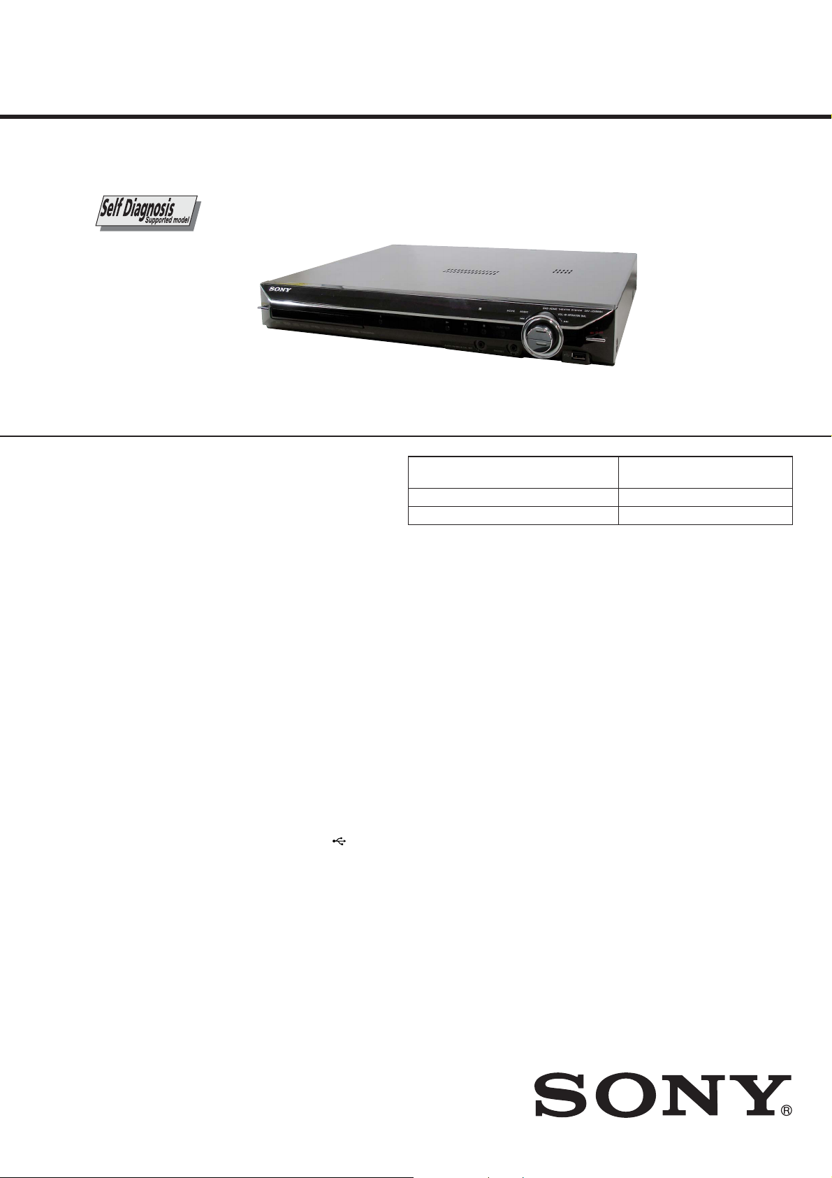
HCD-JZ8888K
SERVICE MANUAL
Ver. 1.0 2009.06
• HCD-JZ8888K is the amplifi er, DVD/CD
and tuner section in DAV-JZ8888K.
This system incorporates with Dolby* Digital and Dolby Pro
Logic (II) adaptive matrix surround decoder and the DTS** Digital
Surround System.
* Manufactured under license from Dolby Laboratories.
Dolby, Pro Logic, and the double-D symbol are trademarks of
Dolby Laboratories.
** Manufactured under license under U.S. Patent #’s:
5,451,942; 5,956,674; 5,974,380; 5,978,762; 6,487,535 & other
U.S. and worldwide patents issued & pending. DTS and DTS
Digital Surround are registered trademarks and the DTS logos
and Symbol are trademarks of DTS, Inc. © 1996-2008 DTS, Inc.
All Rights Reserved.
Model Name Using Similar Mechanism
Mechanism Type CDM85-DVBU102
Optical Pick-up Name KHM-313CAA
E Model
HCD-DZ290K/DZ295K/DZ390K/
DZ590K/DZ690K/DZ790K
Amplifi er Section
Stereo mode (rated) 108 W + 108 W (at 3 ohms,
1 kHz, 1% THD)
Surround mode (reference) RMS output power
FL/FR/C/SL/SR*: 144
watts (per channel at 3
ohms, 1 kHz, 10% THD)
Subwoofer L/Subwoofer
R*: 140 watts (at 3 ohms,
80 Hz, 10% THD)
* Depending on the decoding mode settings and the
source, there may be no sound output.
Inputs (Analog)
TV (AUDIO IN) Sensitivity: 450/250 mV
SAT/CABLE (AUDIO IN) Sensitivity: 450/250 mV
AUDIO IN/MIC Sensitivity: AUDIO IN
250/125 mV/MIC 1 mV
Inputs (Digital)
TV (COAXIAL IN/OPTICAL IN)
Impedance: 75 ohms/ Input Stream: Dolby
Digital 5.1ch/DTS 5.1ch/
Linear PCM 2ch
(Sampling Frequency: less
than 48 kHz)
Outputs (Analog)
Phones Accepts low- and high impedance headphones.
SPECIFICATIONS
Super Audio CD/DVD System
Laser Diode Properties Emission Duration:
Continuous
Laser Output: Less than
44.6μW
* This output is the value measurement at a distance
of 200mm from the objective lens surface on the
Optical Pick-up Block with 7mm aperture.
Signal format system
Mexican and Latin American models:
NTSC
Other models: NTSC/PAL
USB Section
(USB) port:
Maximum current: 500 mA
Tuner Section
System PLL quartz-locked digital
synthesizer
FM Tuner section
Tuning range
North American models: 87.5 MHz - 108.0 MHz
(100 kHz step)
Other models: 87.5 MHz - 108.0 MHz
(50 kHz step)
Antenna (aerial) FM wire antenna (aerial)
Antenna (aerial) terminals 75 ohms, unbalanced
Intermediate frequency 10.7 MHz
Video Section
Outputs VIDEO: 1 Vp-p 75 ohms
COMPONENT:
Y: 1 Vp-p 75 ohms
P
75 ohms
HDMI OUT: Type A (19 pin)
General
Power requirements
Mexican models: 120 V AC, 60 Hz
Latin American models: 110 V - 240 V AC,
50/60 Hz
Other models: 220 V - 240 V AC,
50/60 Hz
Power consumption On: 185 W
Standby: 0.3 W (at the
Power Saving mode)
Output voltage (DIGITAL MEDIA PORT)
DC 5 V
Output current (DIGITAL MEDIA PORT)
700 mA
Dimensions (approx.) 430 mm × 66 mm × 390 mm
(w/h/d) incl. projecting parts
Mass (approx.) 4.3 kg
B/CB, PR/CR: 0.7 Vp-p
– Continued on next page –
DVD RECEIVER
9-889-548-01
2009F04-1
2009.06
©
Sony Corporation
Audio&Video Business Group
Published by Sony Techno Create Corporation
HCD-JZ8888K
Supported fi le format
MP3 (MPEG 1 Audio Layer-3)
File Extension: mp3
Bitrate: 32 kbps - 320 kbps
Sampling frequencies: 32/44.1/48 kHz
WMA (USB device only)
File Extension: wma
Bitrate: 48 kbps - 192 kbps
Sampling frequencies: 44.1 kHz
AAC (USB device only)
File Extension: m4a
Bitrate: 48 kbps - 320 kbps
Sampling frequencies: 44.1 kHz
DivX
File Extension: avi/divx
Video codec: DivX video
Bitrate: 8 Mbps (MAX)
Frame rate: 30 fps
Resolution: 720 × 576
Audio codec: MP3
MPEG4
File format: MP4 File Format
File Extension: mp4/m4v
Video codec: MPEG4 Simple Profi le
(AVC is not compatible.)
Bitrate: 4 Mbps
Frame rate: 30 fps
Resolution: 720 × 576
Audio codec: AAC-LC (HE-AAC is not
compatible.)
DRM: Not compatible
Design and specifi cations are subject to change
without notice.
MODEL IDENTIFICATION
– Back Panel –
Model Part No.
E32 model
MX model
SP model
• Abbreviation
E32 : 110 – 240V AC area in E model
MX : Mexican model
SP : Singapore model
Parts No.
4-122-169-0[]
4-122-169-1[]
4-122-169-3[]
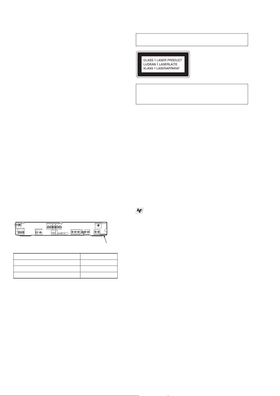
Laser component in this product is capable of emitting radiation
exceeding the limit for Class 1.
This appliance is classifi ed as
a CLASS 1 LASER product.
This marking is located on the
rear or bottom exterior.
CAUTION
Use of controls or adjustments or performance of procedures
other than those specifi ed herein may result in hazardous radia-
tion exposure.
NOTES ON CHIP COMPONENT REPLACEMENT
• Never reuse a disconnected chip component.
• Notice that the minus side of a tantalum capacitor may be damaged by heat.
FLEXIBLE CIRCUIT BOARD REPAIRING
• Keep the temperature of soldering iron around 270 °C during
repairing.
• Do not touch the soldering iron on the same conductor of the
circuit board (within 3 times).
• Be careful not to apply force on the conductor when soldering
or unsoldering.
UNLEADED SOLDER
Boards requiring use of unleaded solder are printed with the leadfree mark (LF) indicating the solder contains no lead.
(Caution: Some printed circuit boards may not come printed with
the lead free mark due to their particular size)
: LEAD FREE MARK
Unleaded solder has the following characteristics.
• Unleaded solder melts at a temperature about 40 °C higher
than ordinary solder.
Ordinary soldering irons can be used but the iron tip has to be
applied to the solder joint for a slightly longer time.
Soldering irons using a temperature regulator should be set to
about 350 °C.
Caution: The printed pattern (copper foil) may peel away if
the heated tip is applied for too long, so be careful!
• Strong viscosity
Unleaded solder is more viscous (sticky, less prone to fl ow)
than ordinary solder so use caution not to let solder bridges
occur such as on IC pins, etc.
• Usable with ordinary solder
It is best to use only unleaded solder but unleaded solder may
also be added to ordinary solder.
SAFETY-RELATED COMPONENT WARNING!
COMPONENTS IDENTIFIED BY MARK 0 OR DOTTED LINE
WITH MARK 0 ON THE SCHEMATIC DIAGRAMS AND IN
THE PARTS LIST ARE CRITICAL TO SAFE OPERATION.
REPLACE THESE COMPONENTS WITH SONY PARTS
WHOSE PART NUMBERS APPEAR AS SHOWN IN THIS
MANUAL OR IN SUPPLEMENTS PUBLISHED BY SONY.
2
SPECIAL COMPONENT NOTICE
The components identifi ed by mark 9 contain confi dential infor-
mation.
Strictly follow the instructions whenever the components are repaired and/or replaced.

TABLE OF CONTENTS
HCD-JZ8888K
1. SERVICING NOTES
............................................. 4
2. DISASSEMBLY
2-1. Case ................................................................................ 7
2-2. Front Panel Section ......................................................... 7
2-3. Back Panel Section ......................................................... 8
2-4. DVD Mechanism Deck ................................................... 8
2-5. POWER Board, USB Board ........................................... 9
2-6. MAIN Board, SP Board, DSP Board .............................. 9
2-7. IO-COMPONENT Board ............................................... 10
2-8. Tray ................................................................................. 10
2-9. Belt .................................................................................. 11
2-10. MS-203 Board ................................................................. 11
2-11. Base Unit ......................................................................... 12
2-12. Optical Pick-up ............................................................... 12
3. TEST MODE ............................................................ 13
4. ELECTRICAL ADJUSTMENTS ........................ 19
5. DIAGRAMS
5-1. Block Diagram –RF Section– ......................................... 21
5-2. Block Diagram –VIDEO Section– ................................. 22
5-3. Block Diagram –AUDIO Section– ................................. 23
5-4. Block Diagram –DSP Section– ....................................... 24
5-5. Block Diagram –AMP Section– ..................................... 25
5-6. Block Diagram –POWER Section– ................................ 26
5-7. Printed Wiring Board –MAIN Section (1/2)– ................. 28
5-8. Printed Wiring Boards –MAIN Section (2/2)– ............... 29
5-9. Schematic Diagram –MAIN Section (1/10)– ................. 30
5-10. Schematic Diagram –MAIN Section (2/10)– ................. 31
5-11. Schematic Diagram –MAIN Section (3/10)– ................. 32
5-12. Schematic Diagram –MAIN Section (4/10)– ................. 33
5-13. Schematic Diagram –MAIN Section (5/10)– ................. 34
5-14. Schematic Diagram –MAIN Section (6/10)– ................. 35
5-15. Schematic Diagram –MAIN Section (7/10)– ................. 36
5-16. Schematic Diagram –MAIN Section (8/10)– ................. 37
5-17. Schematic Diagram –MAIN Section (9/10)– ................. 38
5-18. Schematic Diagram –MAIN Section (10/10)– ............... 39
5-19. Printed Wiring Board –IO-COMPONENT Section– ...... 40
5-20. Schematic Diagram –IO-COMPONENT Section– ........ 41
5-21. Printed Wiring Board –DSP Section (1/2)– .................... 42
5-22. Printed Wiring Board –DSP Section (2/2)– .................... 43
5-23. Schematic Diagram –DSP Section– ................................ 44
5-24. Printed Wiring Board –SCORE Section– ....................... 45
5-25. Schematic Diagram –SCORE Section– .......................... 46
5-26. Printed Wiring Boards –FL-JACK, KEY-SW Section– .. 47
5-27. Schematic Diagram –FL-JACK Section– ....................... 48
5-28. Printed Wiring Boards –LED Section– ........................... 49
5-29. Schematic Diagram –LED Section– ............................... 50
5-30. Printed Wiring Boards –SP, USB Section– ..................... 51
5-31. Schematic Diagram –SP, USB Section– ......................... 52
5-32. Printed Wiring Board –POWER Section– ...................... 53
5-33. Schematic Diagram –POWER Section– ......................... 54
6. EXPLODED VIEWS
6-1. Overall Section ............................................................... 73
6-2. Front Panel Section ......................................................... 74
6-3. Chassis Section ............................................................... 75
6-4. DVD Mechanism Deck Section (CDM85-DVBU102) .. 76
7. ELECTRICAL PARTS LIST .............................. 77
3
HCD-JZ8888K
SECTION 1
SERVICING NOTES
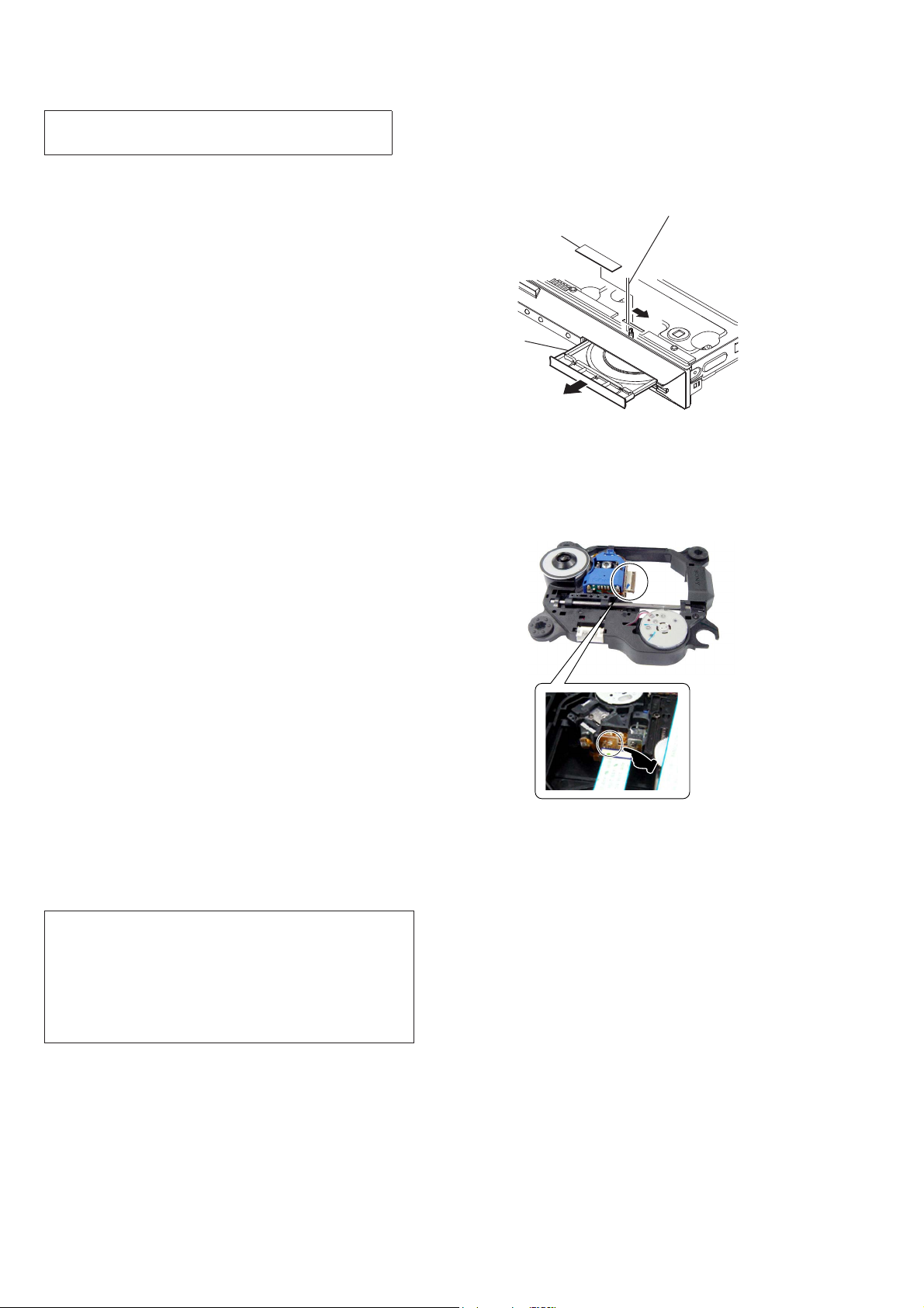
NOTES ON HANDLING THE OPTICAL PICK-UP
BLOCK OR BASE UNIT
The laser diode in the optical pick-up block may suffer electrostatic break-down because of the potential difference generated by
the charged electrostatic load, etc. on clothing and the human body.
During repair, pay attention to electrostatic break-down and also
use the procedure in the printed matter which is included in the
repair parts.
The fl exible board is easily damaged and should be handled with
care.
NOTES ON LASER DIODE EMISSION CHECK
The laser beam on this model is concentrated so as to be focused
on the disc refl ective surface by the objective lens in the optical
pickup block. Therefore, when checking the laser diode emission,
observe from more than 30 cm away from the objective lens.
LASER DIODE AND FOCUS SEARCH
1. Open the case and turn POWER on with no disc inserted.
2. Confi rm that the following operation is performed while
observing the objecting lens from the clearance of DVD
mechanism deck.
1) Confi rm that laser beam is spread.
2) Up and down motion of the objective lens. (2 times)
DISC TRAY LOCK
The disc tray lock function for the antitheft of an demonstration
disc in the store is equipped.
Setting Procedure :
1. Press the [
2. Press the [FUNCTION] button to set DVD function.
3. Insert a disc.
4. Press the [x] button and the [Z] button simultaneously for fi ve
seconds.
5. The message “LOCKED” is displayed and the tray is locked.
Releasing Procedure :
1. Press the [x] button and the [Z] button simultaneously for fi ve
seconds again.
2. The message “UNLOCKED” is displayed and the tray is
unlocked.
Note: When “LOCKED” is displayed, the tray lock is not released by
turning power on/off with the [
On cleaning discs, disc/lens cleaners
• Do not use cleaning discs or disc/lens cleaners (including wet
or spray types). These may cause the apparatus to malfunction.
IMPORTANT NOTICE
Caution: This system is capable of holding a still video image or
on-screen display image on your television screen indefi nitely.
If you leave the still video image or on-screen display image
displayed on your TV for an extended period of time you risk
permanent damage to your television screen.
Projection televisions are especially susceptible to this.
] button to turn the set on.
?/1
?/1
] button.
How to open the disc table when power switch turns off
Insert a tapering driver into the aperture of the unit bottom, and
slide it in the direction of the arrow.
Peel off the lavel and so the lever is moved
in the direction of the arrow with the thin rod.
lavel
tray
Precaution when installing a new OP unit/
Precaution before unsoldering the static electricity
prevention solder bridge
When installing a new OP unit, be sure to connect the fl exible
printed circuit board fi rst of all before removing the static electricity
prevention solder bridge by unsoldering.
Remove the static electricity prevention solder bridge by
unsoldering after the fl exible printed circuit board has already been
connected.
(Do not remove nor unsolder the solder bridge as long as the OP
unit is kept standalone.)
Attention when transported
Use this mode when returning the set to the customer after repair.
Procedure:
1. Press the [
2. Press the [FUNCTION] button to set the function “DVD”.
3. Remove all discs, and then press two buttons [
simultaneously.
4. After a message “MECHA LOCK” is displayed on the
fl uorescent indicator tube, pull out the AC plug.
5. To exit from this mode, press the [
on.
] button to turn the set on.
?/1
] and [
N
] button to turn the set
?/1
?/1
]
4
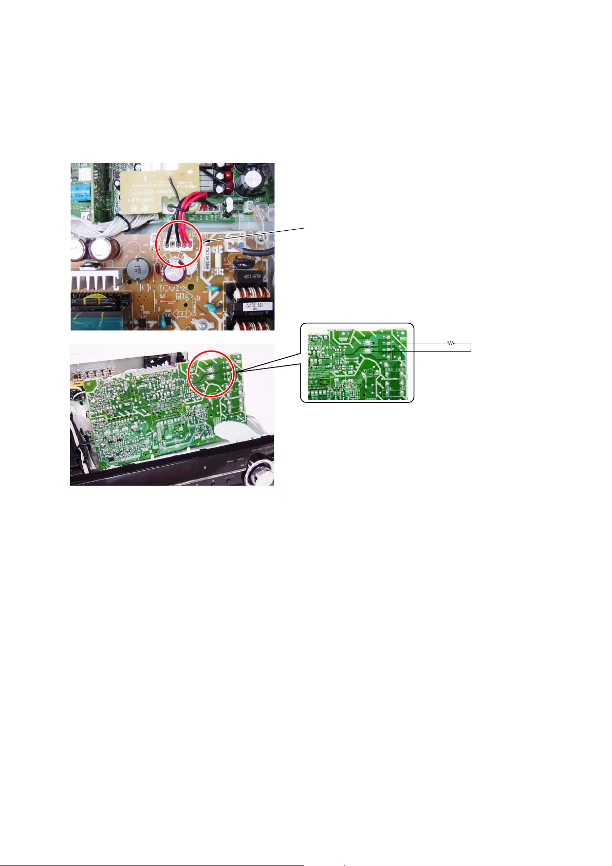
Discharge the charged electricity in capacitors to prevent electric shock as follows
When disassembling the machine, be sure to discharge the charged electricity in the following capacitors.
Use a resistor of 800 ohms, 2 Watts for discharging the following capacitors.
POWER board
C903: 390V
C932, C933, C934, CN904: 30V
Point of capacitor discharge for C932, C933, C934:
Connect to the red and black wire of CN904.
HCD-JZ8888K
Point of capacitor discharge for C903:
Connect to the foot of C903.
800:/2W
5
HCD-JZ8888K
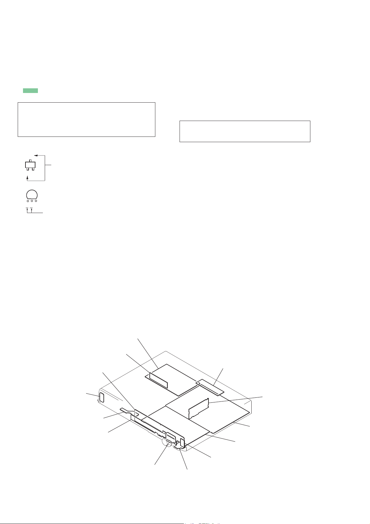
DISASSEMBLY
• This set can be disassembled in the order shown below.
SET
2-1. CASE
(Page 7)
2-2. FRONT PANEL SECTION
(Page 7)
2-3. BACK PANEL SECTION
(Page 8)
2-4. DVD MECHANISM DECK
(Page 8)
SECTION 2
2-5. POWER BOARD,
USB BOARD
(Page 9)
2-6. MAIN BOARD,
SP BOARD,
DSP BOARD
(Page 9)
2-7. IO-COMPONENT BOARD
(Page 10)
2-8. TRAY
(Page 10)
2-9. BELT
(Page 11)
2-10. MS-203 BOARD
(Page 11)
2-11. BASE UNIT
(Page 12)
2-12. OPTICAL PICK-UP
(Page 12)
6
Note: Follow the disassembly procedure in the numerical order given.
HCD-JZ8888K
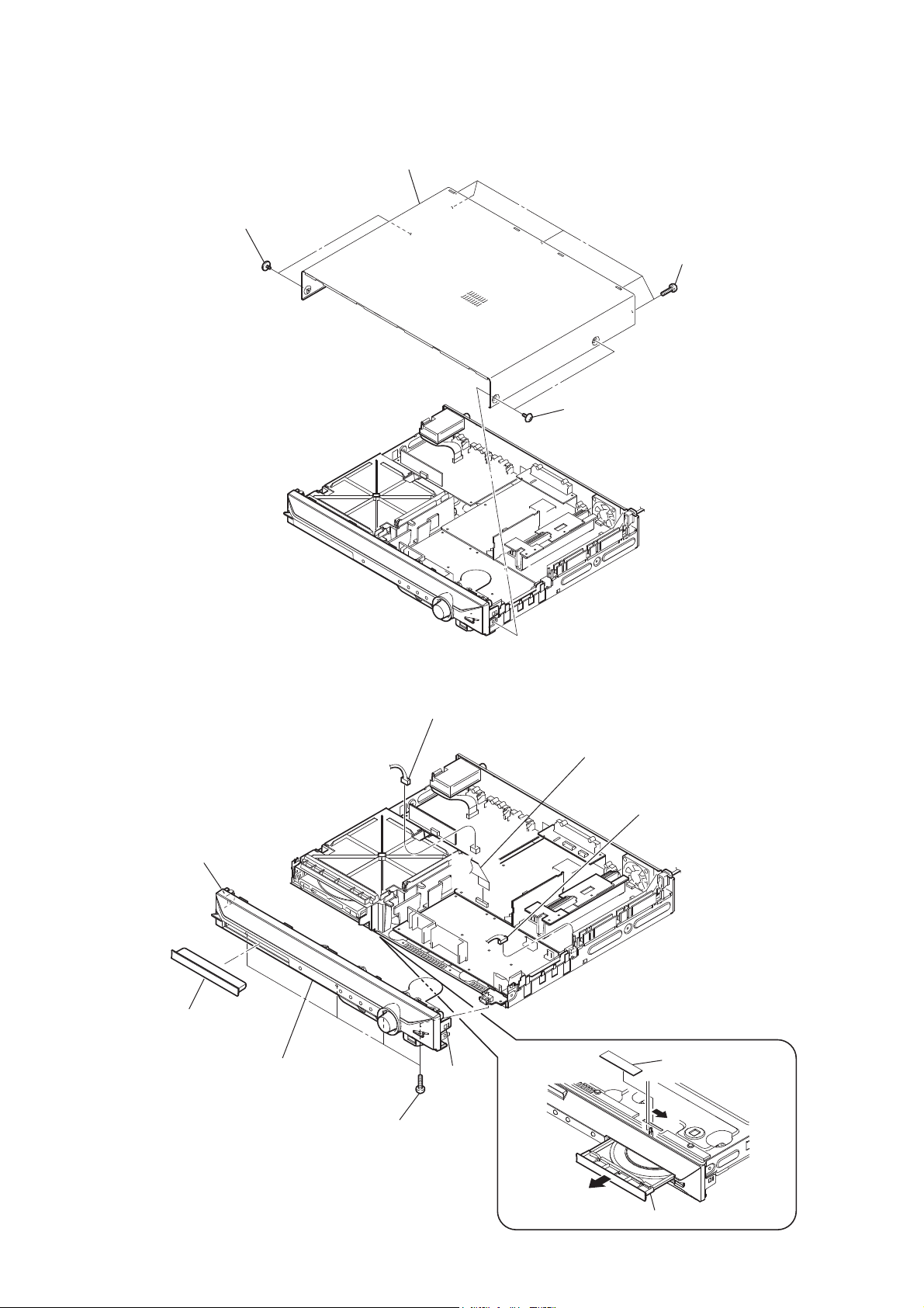
2-1. CASE
4 case
2 two screws
(case 3 TP2)
3 five screws
(BV/ring)
1 two screws
(case 3 TP2)
2-2. FRONT PANEL SECTION
9 claw
4 loading panel
0 front panel section
5 CN4014 (4P)
9 claw
8 four screws
(+BV3 (3-CR))
6 wire (flat type)(19 core)
(CN507)
7 CN3001 (3P)
1 label
2
3
tray
7
HCD-JZ8888K
2-3. BACK PANEL SECTION
3 wire (flat type) (9 core)
(CN4016)
0 back panel section
4 three screws
(+BVTP 3 u8)
5 two screws
(+BVTP 3 u8)
6 two screws
(+BVTP 3 u8)
7 screw
(+B 3 u6)
8 two screws
(+BVTP 3 u8)
9 screw
(+BVTP 3 u8)
2 CN3000 (2P)
1 CN901 (2P)
2-4. DVD MECHANISM DECK
4 screw
(+BV3 (3-CR))
7 cover (CDM-DSY)
8 two screws
(+BV3 (3-CR))
0 DVD mechanism deck
5 screw
(+BV3 (3-CR))
6 screw
(+BV3 (3-CR))
9 screw
(+BV3 (3-CR))
3 wire (flat type)(5 core)
(CN1202)
2 CN1201 (6P)
1 wire (flat type)(24 core)
(CN1101)
8
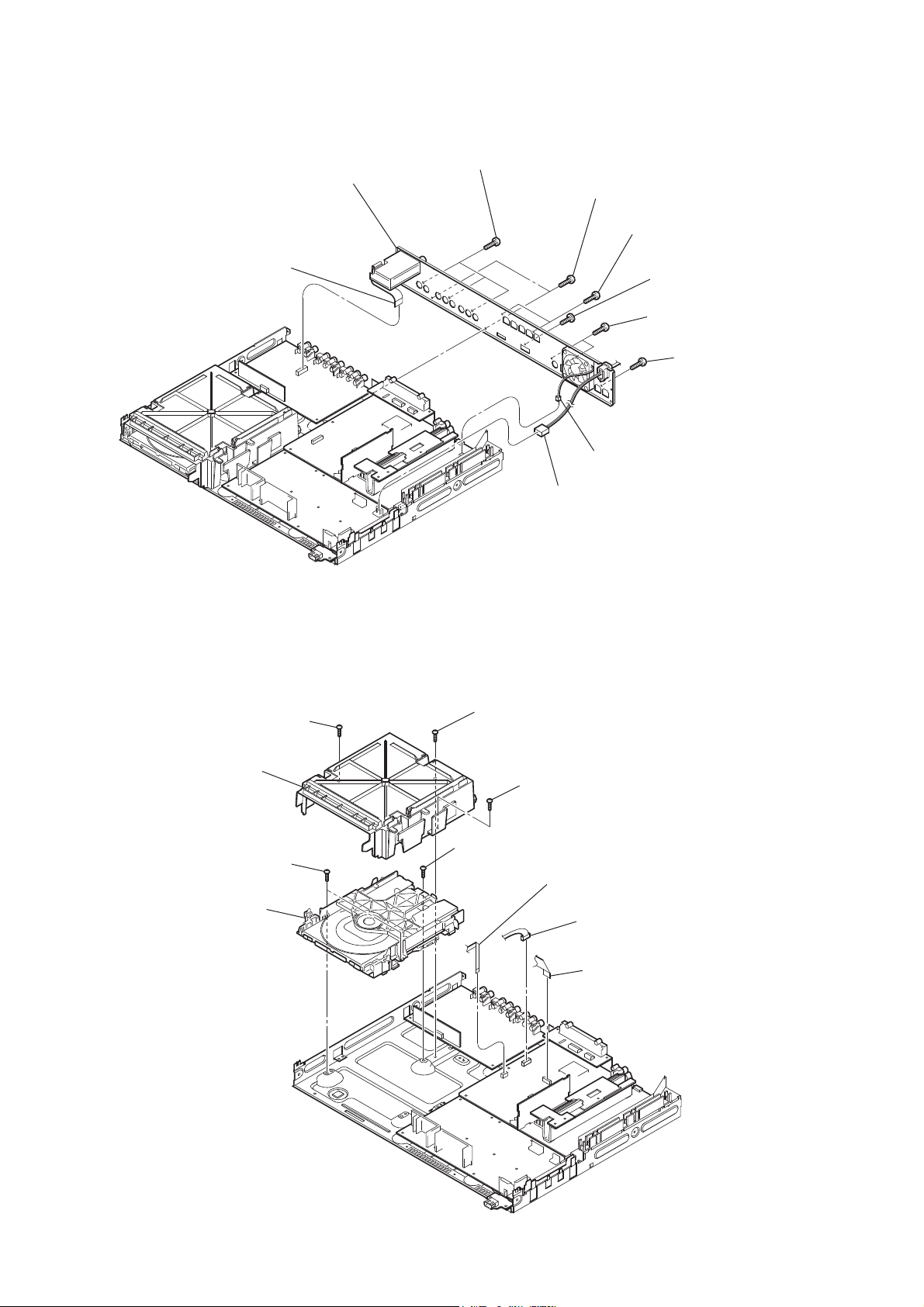
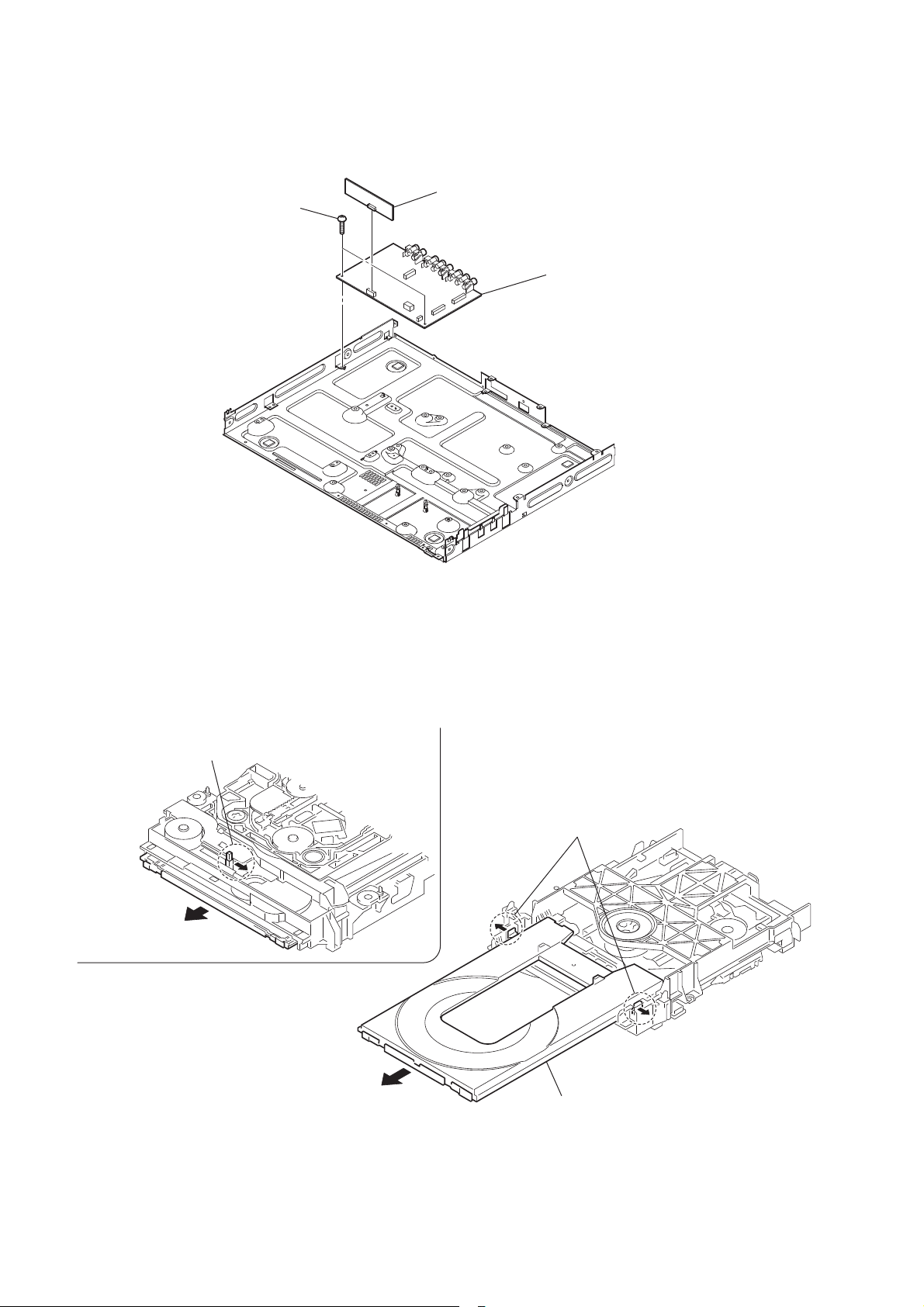
2-5. POWER BOARD, USB BOARD
HCD-JZ8888K
qd three screws
(+PWH 3 u8)
qh POWER board
1 two screws
(+BV3 (3-CR))
7 CN906 (13P)
qf three screws
(+PWH 3 u8)
8 CN904 (4P)
qa screw
(+BV3 (3-CR))
qs cover (rear)
9 screw
(+BV3 (3-CR))
0 cover (front)
4 two screws
(+BVTP 3 u8)
5 plate (POW) insulated
6 bracket (POW-DSY)
(SP model)
2 CN5201 (5P)
3 USB board
2-6. MAIN BOARD, SP BOARD, DSP BOARD
qs three screws
5 wire (flat type) (17 core) (CN472)
6 wire (flat type) (7 core) (CN302)
7 wire (flat type) (17 core) (CN503)
qg six screws
9 screw
(+BV3 (3-CR))
0 screw
(+BV3 (3-CR))
8 CN700 (3P)
qa DSP board
(+BV3 (3-CR))
lug
(+BV3 (3-CR))
qg two holder PC boards
qd heat sink section
4 SP board
3 two screws
(+BV3 (3-CR))
qf three radiation sheet
qf four radiation sheet
1 CN303 (4P)
2 CN304 (6P)
qh MAIN board
9
HCD-JZ8888K
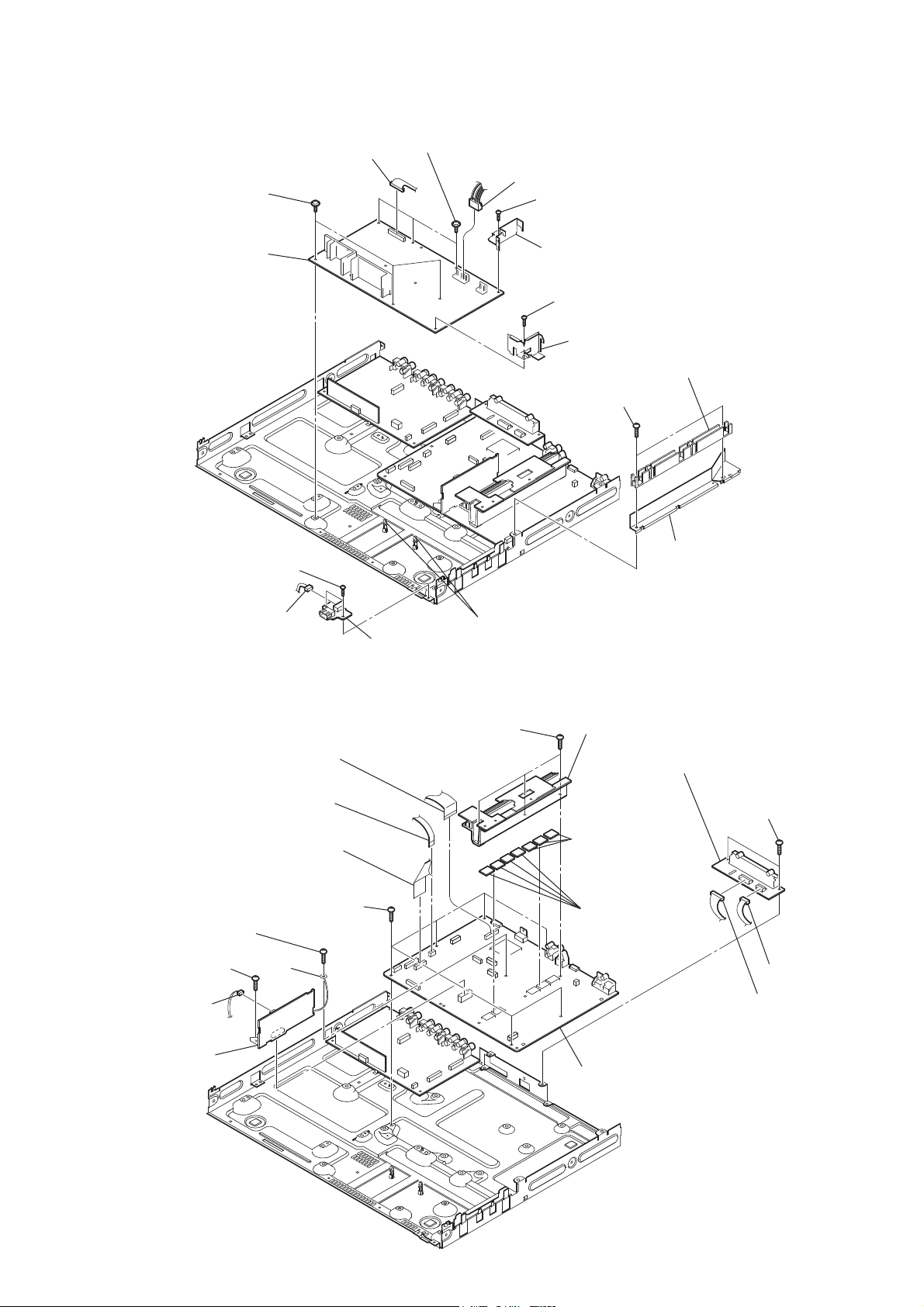
2-7. IO-COMPONENT BOARD
1 two screws
(+BV3 (3-CR))
3 SCORE board
2 IO-COMPONENT board
2-8. TRAY
Move the chuck cam
in the direction of the arrow.
bottom side
two claws
tray
10
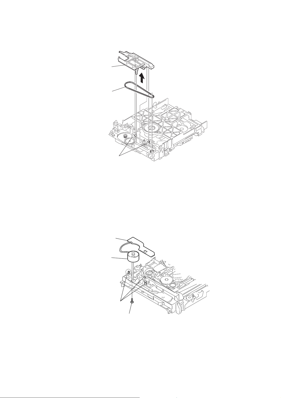
2-9. BELT
chuck cam
HCD-JZ8888K
belt
2-10. MS-203 BOARD
two claws
MS-203 board
DC motor
three claws
screw
(M 1.7 × 2.5)
11
HCD-JZ8888K
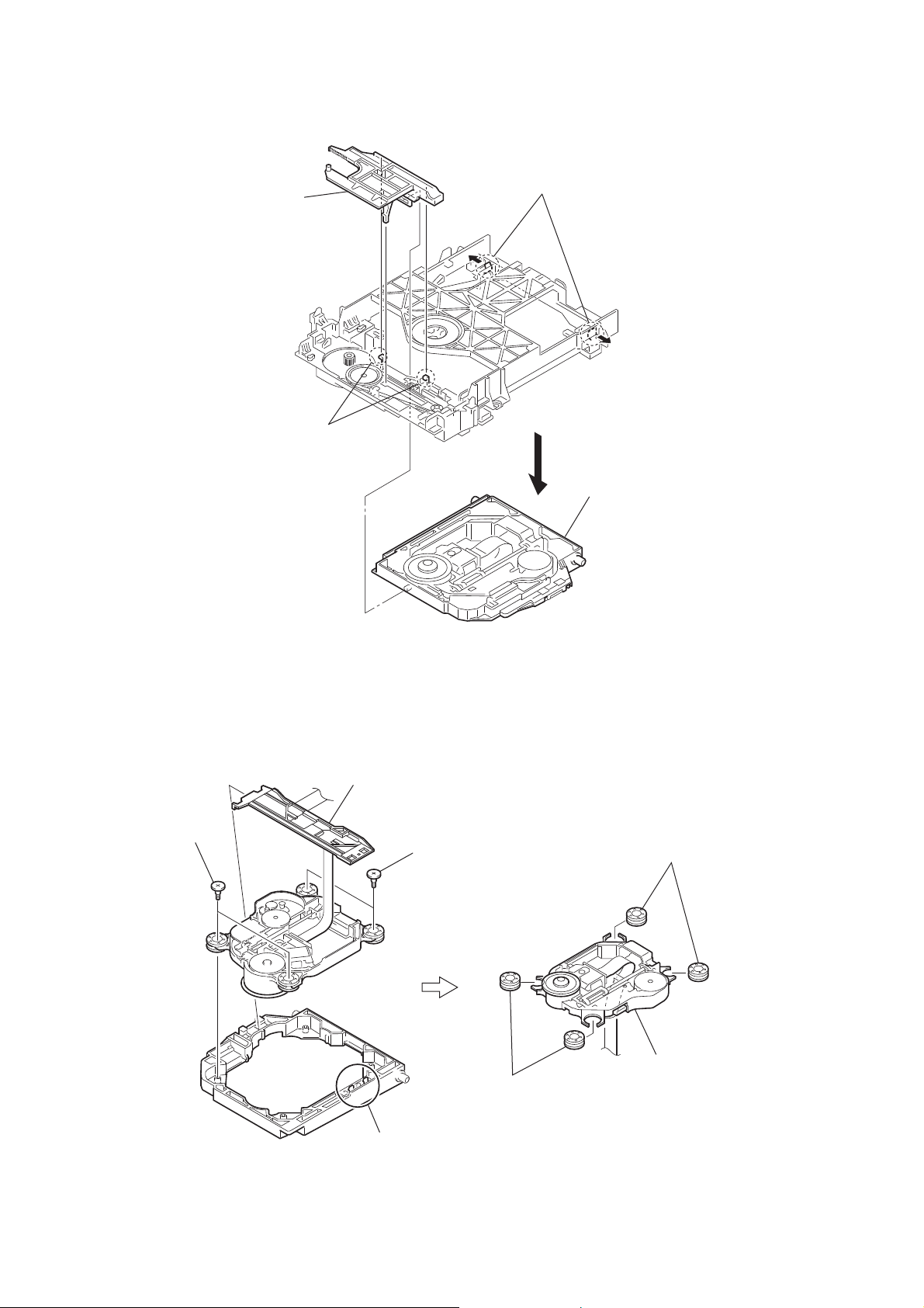
2-11. BASE UNIT
chuck cam
two claws
two claws
base unit
2-12. OPTICAL PICK-UP
two insulator screws
FFC holder
two insulator screws
two claws
two insulators
two insulators
optical pick-up
(KHM-313CAA)
12

SECTION 3
TEST MODE
HCD-JZ8888K
Note: Incorrect operations may be performed if the test mode is not
entered properly.
In this case, press the [?/1] button to turn the power off, and
retry to enter the test mode.
1. Cold Reset
• The cold reset clears all data including preset data stored
in the RAM to initial conditions. Execute this mode when
returning the set to the customers.
Procedure:
1. Press the [
2. Press three buttons [
] button to turn the power on.
?/1
], [N] and [
x
] simultaneously.
?/1
3. When this button is operated, display as “COLD RESET” for
a while and all of the settings are reset.
2. Panel Test Mode
• This mode is used to check the software version, FL and
KEY.
2-1. Display Test Mode
Procedure:
1. Press the [
2. Press three buttons [
] button to turn the power on.
?/1
], [.] and [FUNCTION] simultane-
x
ously.
3. When the display test mode is activated, all segments are turned
on. When the mode in, lamps of “MOVIE”, “MUSIC” and
“i-ENHANCER” are turn off.
4. To exit from this mode, press three buttons [x], [.] and
[FUNCTION] simultaneously.
2-2. Version Test Mode
Procedure:
1. When the display test mode is activated, press the [.] button and the message “TIGRE100K” (JZ8888K) is displayed,
the version test mode is activated.
2. Whenever the [.] button is pressed, the display changes in
the following order.
“TIGRE100K” (Model name) t “AS1A2*1” (Destination) t
t MC Version t SYS Version t UI Version t
t DVD Version t ST Version t TA Version t
t DSP Version t TM Version t MM Version t
t CLA Version t CEC Version t SAIR Version
*1: AS1A2 changes depending on destination.
3. Press the [>] button and the date of the software production
is displayed.
4. Press the [>] button again and the version is displayed.
5. To exit from this mode, press three buttons [x], [.] and
[FUNCTION] simultaneously.
2-4. Key Test Mode
Procedure:
1. When the display test mode is activated, press the [N] button,
to select the key test mode.
2. To enter the KEY test mode, the fl uorescent indicator displays
“K0 V0”. Each time an another button is pressed, “KEY” value
increases. However, once a button is pressed, it is no longer
taken into account. When all keys are pressed correctly, “K9
V0” is displayed.
3. When the [VOLUME] control is turned in the direction of (+),
“V0” is changed to “V1”, then ... “V9”.
When the [VOLUME] control is turned in the direction of (–),
“V0” is changed to “V9”, then ... “V1”.
4. To exit from this mode, press three buttons [
], [.] and
x
[FUNCTION] simultaneously.
3. Disc Tray Lock
• The disc tray lock function for the antitheft of an demonstra-
tion disc in the store is equipped.
Setting Procedure :
1. Press the [
] button to turn the set on.
?/1
2. Press the [FUNCTION] button to set DVD function.
3. Insert a disc.
4. Press the [x] button and the [Z] button simultaneously for fi ve
seconds.
5. The message “LOCKED” is displayed and the tray is locked.
Releasing Procedure :
1. Press the [x] button and the [Z] button simultaneously for fi ve
seconds again.
2. The message “UNLOCKED” is displayed and the tray is unlocked.
Note: When “LOCKED” is displayed, the tray lock is not released by
turning power on/off with the [?/1] button.
4. DVD Ship Mode
• Use this mode when returning the set to the customer after
repair.
Procedure:
1. Press the [
] button to turn the set on.
?/1
2. Press the [FUNCTION] button to set the function “DVD”.
3. Remove all discs, and then press two buttons [N] and [
?/1
simultaneously.
4. After a message “MECHA LOCK” h “UNPLUG” is displayed on the fl uorescent indicator tube, pull out the AC plug.
5. To exit from this mode, press the [
] button to turn the set
?/1
on.
]
2-3. FL Pattern Test Mode
Procedure:
1. When the display test mode is activated, press the [x] button,
to select the FL pattern test mode. When the FL pattern test
mode, half segments of FL display and lamps of “MOVIE”,
“REC TO USB” are turn on.
2. Press the [x] button, half segments of FL display and lamp of
“MUSIC” and “
, VOLUME Illumination” are turn on.
"/1
3. Next press the [x] button, all segments of FL display is turn
on.
4. To exit from this mode, press three buttons [x], [.] and
[FUNCTION] simultaneously.
13

HCD-JZ8888K
5. Product Out
• This mode moves the optical pick-up to the position durable
to vibration and clears all data including preset data stored in
the RAM to initial conditions. Use this mode when returning
the set to the customer after repair.
Procedure:
1. Press the [
] button to turn the power on.
?/1
2. Press the [FUNCTION] button to set the function “DVD”.
3. Remove all discs, and then press three buttons [x], [Z] and
[VOLUME+] simultaneously.
4. Displayed to message “SERVICE IN” on the fl uorescent indi-
cator tube when pressing in turn the [4] t [DVD MENU] t
[CLEAR] buttons on the remote commander.
5. After the “STANDBY” blinking display fi nishes, the message
“MECHA LOCK” h “UNPLUG” is displayed on the fl uo-
rescent indicator tube disconnect the AC power plug, then the
product out mode is set.
6. Color System Change (Except E32 model)
• Color system change to video signal format (NTSC/PAL).
Procedure:
1. Press the [
] button to turn the set on.
?/1
2. Press the [FUNCTION] button to set the function “DVD”.
3. Press the [
4. Press two buttons [.] and [
] button to turn the set OFF.
?/1
?/1
] simultaneously, and the
display of fl uorescent indicator tube changes to “COLOR
PAL” or “COLOR NTSC”.
DVD SECTION
7-1. GENERAL DESCRIPTION
• The IOP measurement allows you to make diagnosis and adjustment simply by using the remote commander and monitor TV. The instructions, diagnosis results, etc. are given on
the on-screen display (OSD).
Be sure to execute the IOP measurement when a BU (Base
Unit) is replaced.
7-2. HOW TO ENTER TEST MODE
While pressing the [
[VOLUME] control in the direction of (+) with the DVD player
in power on.
The Test Mode starts, displayed “SERVICE IN” on this model
display then the menu shown below will be displayed on the TV
screen.
* The display of the “Model Name” of the “Remocon Diagnosis
Menu” change with the model and the destination. Refer to
below on the model name.
JZ8888K : TIGRE100K
Remocon Diagnosis Menu
0. External Chip Check
1. Servo Parameter Check
2. Drive Manual Operation
3. Emergency History
4. Version Information
] and [Z] buttons simultaneously, turn
x
1
Model Name
IF-con : Ver. XX.XX (XXXX)
Syscon : Ver. X.XXX
*1: Changes depending on destination
: TIGRE100K_XX
*
The menu above is the Remocon Diagnosis Menu screen which
consists of fi ve main functions. At the bottom of the menu screen,
the model name and IF-con version. To exit from the Test Mode,
press the [
] button on the remote commander.
?/1
7-3. EXECUTING IOP MEASUREMENT
In order to execute IOP measurement, the following standard procedures must be followed.
(1) In power on, while pressing the [
] and [Z] buttons simultane-
x
ously, turn the [VOLUME] control in the direction of (+).
Remocon Diagnosis Menu
0. External Chip Check
1. Servo Parameter Check
2. Drive Manual Operation
3. Emergency History
4. Version Information
1
Model Name
IF-con : Ver. XX.XX (XXXX)
Syscon : Ver. X.XXX
*1: Changes depending on destination
: TIGRE100K_XX
*
14
HCD-JZ8888K
(2) Select “2. Drive Manual Operation” by pressing the [2] button
on the remote commander. The screen will appear as shown.
Drive Manual Operation
1. Servo Control
2. Track/Layer Jump
3. Manual Adjustment
4. Tray Aging Mode
5. MIRR time adjust
0. Return to Top Menu
(3) Select “3. Manual Adjustment” by pressing the [3] button on
the remote commander. The screen will appear as shown.
Manual Adjust
1. Track Balance Adjust:
2. Track Gain Adjust:
3. Focus Balance Adjust:
4. Focus Gain Adjust:
5. Eq Boost Adjust:
6. Iop:
7. TRV. Level:
8. S curve(FE) Level:
9. RFL(PI) Level:
0. MIRR Time:
Oo Change Value
[RETURN] Return to previous menu
(4) Select “6. IOP” by pressing the [6] button on the remote
commander.
7-4. EMERGENCY HISTORY
To check the emergency history, please follow the following procedure.
(1) From the Top Menu of Remocon Diagnosis Menu, select “3.
Emergency History Check” by pressing the [3] button on the
remote commander. The following screen appears on the onscreen display.
Emg. History Check
Laser Hours CD
01. 01 05 04 04
00 00 00 00 00 00 23 45
02. 02 02 01 01 00 A9 4B 00
00 00 00 00 00 00 23 45
[Next] Next Page [Prev] Prev Page
[O] Return to Top Menu
999h 59min
DVD 999h 59min
00 92 46 00
(2) You can check the total time when the laser is turned on during
playback of DVD and CD from the above menu. The maximum time, which can be displayed are 999h 59min.
(3) You can check the error code of latest 10 emergency history
from the above menu. To view the previous or next page of
emergency history, press [
] or [>] button on the remote
.
commander. The error code consists of the following three
blocks. The fi rst block indicates the error code. The second
block indicates the parameter and the third block indicates the
time of error code as shown below.
• Error Code
(5) Wait until a hexadecimal number appear.
Manual Adjust
1. Track Balance Adjust:
2. Track Gain Adjust:
3. Focus Balance Adjust:
4. Focus Gain Adjust:
5. Eq Boost Adjust:
6. Iop. 4E:
7. TRV. Level:
8. S curve(FE) Level:
9. RFL(PI) Level:
0. MIRR Time:
Oo Change Value
[RETURN] Return to previous menu
(6) Convert each data from hexadecimal to decimal using
conversion table.
(7) Please fi nd the label on the rear of the BU (Base Unit).
The default IOP value is written in the label.
(8) Subtract between these two values.
(9) If the remainder is smaller than 93 (decimal), then it is
OK. However if the value is higher than 93, then the BU is
defective and need to be change.
(10) Press the [RETURN] button on the remote commander to
return back to previous menu.
(11) Press the [0] button on the remote commander to return to Top
Menu.
Emg. History Check
Laser Hours CD 999h 59min
*1 *2
01. 01 05 04 04
00 00 00 00 00 00 23 45
02. 02 02 01 01 00 A9 4B 00
00 00 00 00 00 00 23 45
[Next] Next Page [Prev] Prev Page
[O] Return to Top Menu
DVD 999h 59min
00 92 46 00
*3
*1 : Error Code
*2 : Parameter of error code
*3 : Time of error code
The meaning of error code is as below:
01: Communication error (No reply from syscon)
02: Syscon hung up
03: Power OFF request when syscon hung up
19: Thermal shutdown
24: MoveSledHome error
25: Mechanical move error (5 Changer)
26: Mechanical move stack error
30: DC motor adjustment error
31: DPD offset adjustment error
32: TE balance adjustment error
33: TE sensor adjustment error
34: TE loop gain adjustment error
35: FE loop gain adjustment error
36: Bad jitter after adjustment
40: Focus NG
42: Focus layer jump NG
51: Spindle stop error
52: Open kick spindle error
15

HCD-JZ8888K
60: Focus on error
61: Seek fail error
62: Read Q data/ID error
70: Lead in data read fail
71: TOC read time out (CD)
80: Can’t buffering
81: Unknown media type
7-4-1. Clear the Laser Hour
Press [
DISPLAY] button and then press [CLEAR] button on the
remote commander. The data for both CD and DVD data are reset.
Emg. History Check
Laser Hours CD 0h 0min
01. 01 05 04 04
00 00 00 00 00 00 23 45
02. 02 02 01 01 00 A9 4B 00
00 00 00 00 00 00 23 45
[Next] Next Page [Prev] Prev Page
[O] Return to Top Menu
DVD 0h 0min
00 92 46 00
7-4-2. Clear the Emergency History
Press [DVD TOP MENU] button and then press [CLEAR] button
on the remote commander. The error code for all emergency history would be reset.
Emg. History Check
7-4-4. Return to the Top Menu of Remocon Diagnosis
Menu
Press [0] button on the remote commander.
7-5. CHECK VERSION INFORMATION
To check the version information, please follow the following procedure.
(1) From the Top Menu of Remocon Diagnosis Menu, select “4.
Version Information” by pressing the [4] button on the remote
commander. The following screen appears on the on-screen
display.
Version information
Firm (Main) : Ver. xxxxx
Firm (Sub) : xxxxx
RISC : xxxxx
8032 : xxxxx
Audio DSP : xxxxx
Servo DSP : xxxxx
Phy,Adr, : F.F.F.F
[O] Return to Top Menu
To return to the Top Menu of Remocon Diagnosis Menu, press
[0] button on the remote commander.
8. D.C.A.C. (AUTOMATIC ACOUSTIC FIELD CALIBRATION) TEST MODE
Laser Hours CD 999h 59min
01. 00 00 00 00
00 00 00 00 00 00 00 00
02. 00 00 00 00 00 00 00 00
00 00 00 00 00 00 00 00
[Next] Next Page [Prev] Prev Page
[O] Return to Top Menu
DVD 999h 59min
00 00 00 00
7-4-3. Clear the Initialize Setup Data
Press [DVD MENU] button and then press [CLEAR] button on the
remote commander.
Emg. History Check
Laser Hours CD
initialize setup data...
[Next] Next Page [Prev] Prev Page
[O] Return to Top Menu
999h 59min
DVD 999h 59min
Procedure:
1. Press the [
] button to turn the power on.
?/1
2. Press the [FUNCTION] button to set the function “ DVD”.
3. Insert Calibration mic (ECM-AC2) supplied as an accessory
into the AUDIO IN/A.CAL MIC jack.
4. While pressing the [x] and [Z] buttons simultaneously, turn
the [VOLUME] control in the direction of (–).
5. Confi rm that the following are shown on the display panel.
The JACK inserted/non-inserted detection display and the
STEREO/MONO detection display.
JACK :* * * *
1
1 “NON” : Not detected
“ST” : STEREO
“NOMO” : MONO
6. To exit from this mode, press the [x] and [Z] buttons simultaneously, turn the [VOLUME] control in the direction of (–).
16
HCD-JZ8888K
9. AMP TEST MODE
• This mode is used to measurement and test of the AMP connection.
Procedure:
1. Press the [
] button to turn the power on.
?/1
2. Press three buttons [x], [N] and [Z] simultaneously. When
the this mode, blink to segments (“SA-CD” and “CAT”) on FL
display.
3. Press [DISPLAY] button of the remote commander. When the
this mode is displayed as “MEASURE” on FL display.
Whenever the [DISPLAY] button is pressed, the AMP test
mode changes in the following order.
MEASURE t SAFETY
MEASURE: AMP measurement mode
SAFETY: AMP regulations, temperature, character mode
4. Press [MUTING] button on the remote commander. When the
this mode is displayed as “VOL N” on FL display.
Whenever the [MUTING] button is pressed, the VOL test
mode changes in the following order.
VOL N t VOL M/M
VOL N: Turn the [VOLUME] control, the display is
change in succession (MIN y MAX)
VOL M/M: Turn the [VOLUME] control in the direction of
(+) is change to “MIN”, turn the direction of (–)
is change to “MAX”.
5. To exit from this mode, press the [
] button to “COLD RE-
?/1
SET” and turn the power off.
10. DEMO PLAY MODE OUT
It is a mode to release the demonstration reproduct by the dedicated demonstration disc.
1. During playback the DEMO Disc, press the [
] and [N] but-
x
tons for fi ve seconds simultaneously.
2. The message “DEMO OFF” is displayed, a mode to reproduct
the demonstration is released.
11. DMPORT (DIGITAL MEDIA PORT) TEST
1. Connect the DMPORT CHECK JIG (P/N: J-2501-309-A) with
the terminal DMPORT.
2. Press the [
] button to turn the power on.
?/1
3. Confi rm that both LEDs of the DMPORT confi rmation JIG
lights. (Confi rmation the power supply line.)
4. Set the [FUNCTION] button with “DMPORT” on this model.
5. Press three buttons [x], [N] and [FUNCTION] simultaneously, the DMPORT test mode is activated.
6. It is confi rmed that “DMPORT OK” is displayed on this set
display. (Confi rmation of communication line)
7. To a pin jack of the DMPORT confi rmation JIG input informa-
tion relevant to audio signal (sine-wave 1.0Vrms) and composite video signal (white 100% 1.0Vp-p, color bar, etc.)
8. Confi rm the output of speakers and monitor TV. (Confi rmation
of analog signal)
9. To exit from this mode, press three buttons [x], [N] and
[FUNCTION] simultaneously.
VIDEO
AUDIO
color pattern
generator
AF oscillator
DMPORT
CHECK JIG
(P/N: J-2501-309-A)
J001 V
CN451
SET
MAIN
board
IO-COMPONENT
SP board
J4001
TV
board
FL speaker,
FR speaker
TB301
17

HCD-JZ8888K
12. PROTECTION FACTOR (SD DETECTION/
DC DETECTION) IDENTIFICATION TEST MODE
When an error is detected, the FL tube alternately displays
“PROTECTOR h PUSH POWER”.
r Press the [
* Buttons other than the [
“STANDBY” blinks three times on the FL tube.
r
The protection release state (POWER OFF) is established.
(No FL tube display)
r Press the [
The power to the system turns on, and the normal operation is
established. (Restore)
During the protection state:
1. If the AC plug is connected or disconnected during the
protection state, the protection state is released, and the
normal operation is established. (The protection state is not
maintained.)
2. The protection factor is displayed by pressing the [RETURN]
t [3] t [2] t [0] t [0] t [ANGLE] buttons of the
remote commander.
(during the “PROTECTOR h PUSH POWER” display).
k When SD is detected: Repeats
“SD DETECT h PROTECTOR”.
k When DC is detected: Repeats
“DC DETECT h PROTECTOR”.
] button.
?/1
] button two times.
?/1
] button are invalid.
?/1
PL: SD detection
When the “L” output from the SD (shutdown) port on the
S-MASTER POWER Driver Shutdown and voltage descent
(15V or less) of 30V power supply (PVDD) are detected.
DC detection
When the “L” output from the power/speaker error detection
circuit (DC detection port) is detected for two seconds
continually, the power system other than that of the FL tube
is turned off, and the protection state is established.
18
SECTION 4
ELECTRICAL ADJUSTMENTS
DVD SECTION
When the optical pick-up assy is replaced, perform the
“EXECUTING IOP MEASUREMENT”.
EXECUTING IOP MEASUREMENT (See page 14)
TUNER SECTION
[FM Tune Level Check]
generator
HCD-JZ8888K
SET
Procedure:
1. Turn the power on.
2. Input the following signal from Signal Generator to FM antenna input directly.
* Carrier Freq : A = 87.5 MHz, B = 98 MHz, C = 108 MHz
Deviation : 75 kHz
Modulation : 1 kHz
ANT input : 35 dBu (EMF)
Note: Please use 75 ohm “coaxial cable” to connect SG and the set. You
cannot use video cable for checking.
Please use SG whose output impedance is 75 ohm.
3. Set to FM tuner function and tune A, B and C signals.
4. Confi rm “TUNED” is lit on the display for A, B and C signals.
The mark of “TUNED” means “The selected station signal is received in good condition.”
FM ANTENNA
OUT (75 :)
19
HCD-JZ8888K
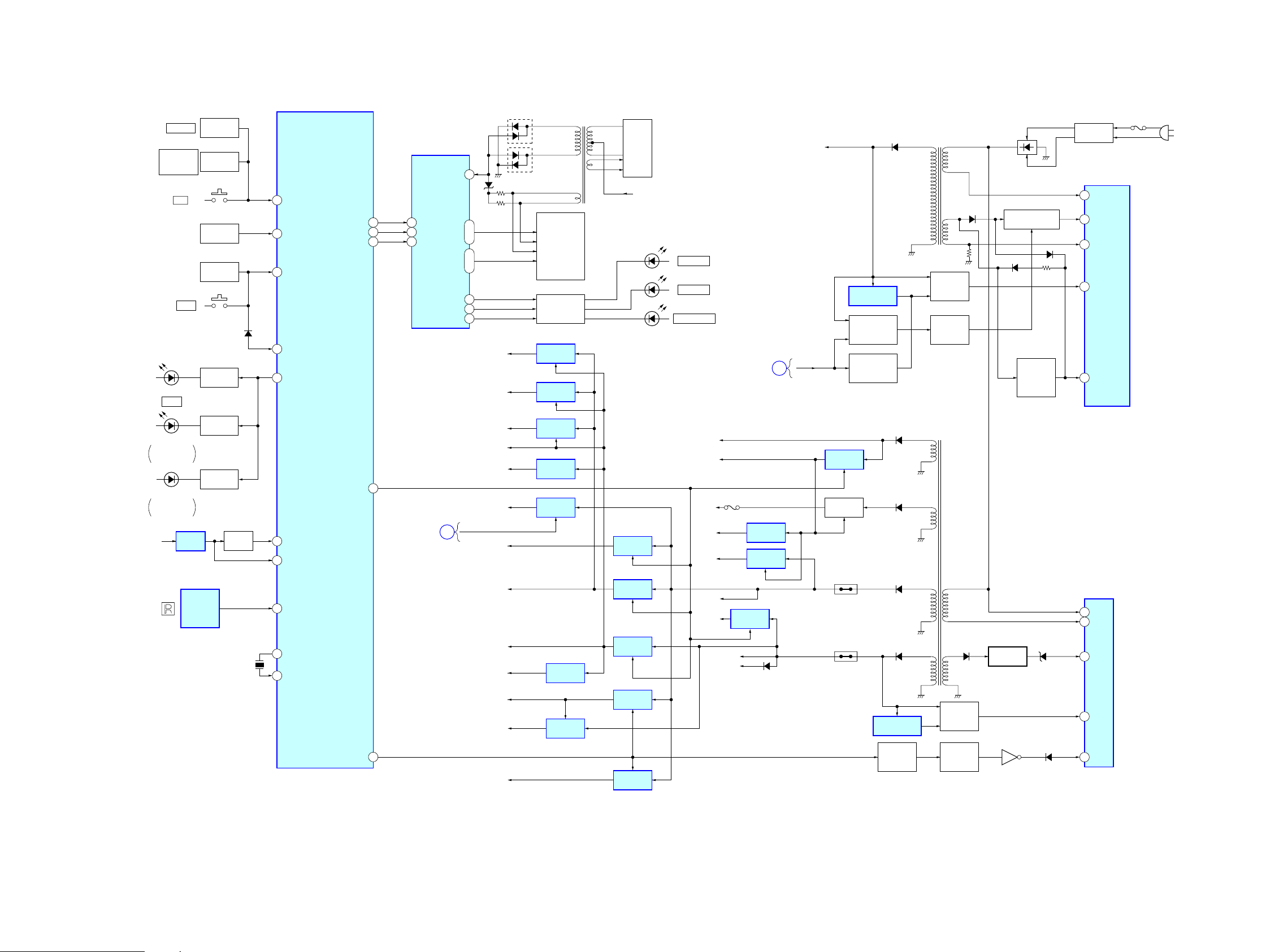
SECTION 5
DIAGRAMS
THIS NOTE IS COMMON FOR PRINTED WIRING BOARDS AND SCHEMATIC DIAGRAMS.
(In addition to this, the necessary note is printed in each block.)
For Printed Wiring Boards.
Note:
• X : Parts extracted from the component side.
• a : Through hole.
• : Pattern from the side which enables seeing.
(The other layers’ patterns are not indicated.)
Caution:
Pattern face side:
(SIDE B)
Parts face side:
(SIDE A)
• Indication of transistor.
C
Q
B
E
CEB
• Abbreviation
E32 : 110 – 240V AC area in E model
MX : Mexican model
SP : Singapore model
These are omitted.
Parts on the pattern face side seen
from the pattern face are indicated.
Parts on the parts face side seen from
the parts face are indicated.
These are omitted.
For Schematic Diagrams.
Note:
• All capacitors are in μF unless otherwise noted. (p: pF) 50
WV or less are not indicated except for electrolytics and
tantalums.
• All resistors are in Ω and 1/4 W or less unless otherwise
specifi ed.
• f : Internal component.
• C : Panel designation.
Note: The components identifi ed by mark 0 or dotted
line with mark 0 are critical for safety.
Replace only with part number specifi ed.
• A : B+ Line.
• B : B– Line.
• Voltages and waveforms are dc with respect to ground
under no-signal (detuned) conditions.
• Voltages and waveforms are dc with respect to ground in
service mode.
• Waveforms are taken with a oscilloscope.
Voltage variations may be noted due to normal production
tolerances.
no mark : TUNER (FM)
< > : DVD PLAY
* : Impossible to measure
• Voltages are taken with VOM (Input impedance 10 MΩ).
• Circled numbers refer to waveforms.
• Signal path.
F : TUNER
J : DVD PLAY
L : VIDEO
E : Y
a : CHROMA
r : COMPONENT VIDEO
N : MIC
• Abbreviation
E32 : 110 – 240V AC area in E model
MX : Mexican model
SP : Singapore model
• Circuit Boards Location
P-LED board
MS-203 board
IO-COMPONENT board
SCORE board
FL-JACK board
KEY-SW board
J-LED board
SP board
DSP board
MAIN board
POWER board
U-LED board
USB board
20
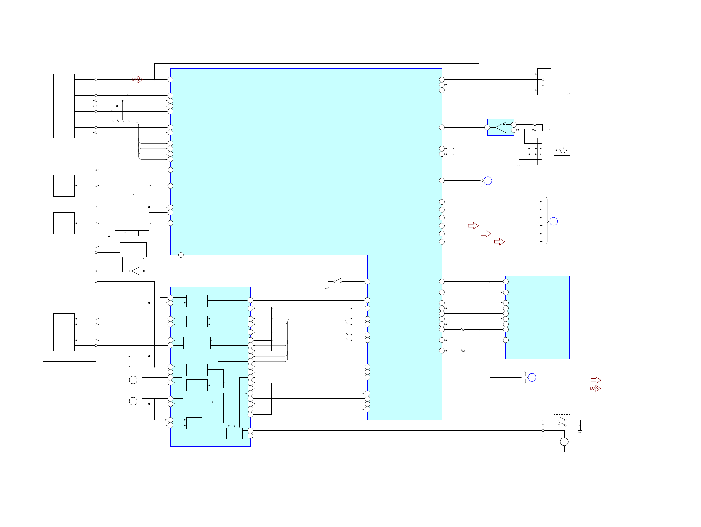
5-1. BLOCK DIAGRAM – RF Section –
RF
VOA/A
DETECTOR
OPTICAL PICK-UP
BLOCK
(KHM-313CAA)
LASER
DIODE
(FOR CD)
LASER
DIODE
(FOR DVD)
VOB/B
VOC/C
VOD/D
VOE/E+G
VOF/F+H
LD (780)
LD (650)
VR (650)
VR (780)
A
B
C
D
A
B
C
D
VC
Q1102 (1/2)
LD DRIVE
CONTROL (FOR CD)
PD
Q1102 (2/2)
LD DRIVE
CONTROL (FOR DVD)
Q1101
PD VOLUME
CONTROL
10
6
7
8
9
17
18
11
12
13
14
28
22
19
20
21
DVDRFIP
DVDA
DVDB
DVDC
DVDD
TNI
TPI
MA
MB
MC
MD
V20 (2.0V)
LD01
MDI1
MDI2
LD02
MSW
54
IC1101 (1/2)
CD/DVD RF AMP,
FOCUS/TRACKING ERROR AMP,
DVD SYSTEM CONTROL, DSP
V2REFO (2.8V)
RXD
TXD
VBUS_OC
USB_DM
USB_DP
VBUS_OE
ACLK
ALRCK
ABCK
ASDATA2
ASDATA1
ASDATA0
27
105
106
VBUS OVER CURRENT DETECT
197 1
45
44
196
203
205
204
223
225
226
VBUS_SW
IC2101
POWER
L
SECTION
(Page 26)
HCD-JZ8888K
CN1105
6
RFMON
5
V2REFO
RXD
TXD
USB 5V
CN5200
SECTION
(Page 24)
(SERVICE JIG)
DSP
2
1
2
3
VBUS
1
D-
2
D+
3
GND
4
ACLK
ALRCK
ABCK
AMP_D02
AMP_D01
AMP_D00
A
2AXIS
DEVICE
FOCUS/
TRACKING
COIL
MSW
VCC
FCS+
FCS-
TRK+
TRK-
REG02
REG01
(SLED MOTOR)
(SPINDLE MOTOR)
Q1103
MM
MM
SP+
SP-
SLSL+
I0P
IC1201
FOCUS/TRACKING DRIVER,
LOADING/SPINDLE/SLED MOTOR DRIVER
42
41
36
37
35
34
32
31
30
29
27
28
46
47
BUFFER
FOCUS COIL
DRIVE
TRACKING COIL
DRIVE
BUFFER
SLED MOTOR
DRIVE
SPINDLE MOTOR
DRIVE
BUFFER
MCS
40
43
48
1
12
3
4
9
10
13
16
17
15
6
7
45
19
20
22
21
25
24
VREFO
FOO
TRO
FMO
DMO
SPFG
(LIMITSW)
FMO
FOO
DMO
TRO
LIMITSW
53
39
IOPMON
VREFO [1.4V]
29
FMO
37
FOO
41
DMO
36
TRO
40
FWD
94
REV
95
38
TROPENPWM
OP_INP
35
MUTE123
157
MUTE
158
TSD_M
130
XSYSRST
IFCK
IFSDO
IFSDI
XIFCS
KMOD
MIC
OCSW
XIFBSY
CKSW
108
98
97
100
99
213
208
104
110
103
XSYSRST
IFSCK
IFSDO
IFSDI
XIFCS
KMOD
MIC
DVD RST
45
DVD_SCO
49
DVD_SDO
48
DVD_SDI
47
DVD XIFCS
51
KMODE
53
TV_SEL/MIC_DET_OUT/LED_LAT
52
CDM_OPEN_SW
44
DVD_XIFBUSY
50
XSYSRST
IC503 (1/6)
SYSTEM CONTROL
VIDEO
C
SECTION
(Page 22)
OCSW1/REVOCSW
CKSW/FWDCKSW
(CHUCK/TRAY DETECT)
LDM+
LDM-
S001
M
SIGNAL PATH
M001
(LOADING MOTOR)
: TUNER
: DVD PLAY
HCD-JZ8888K
2121
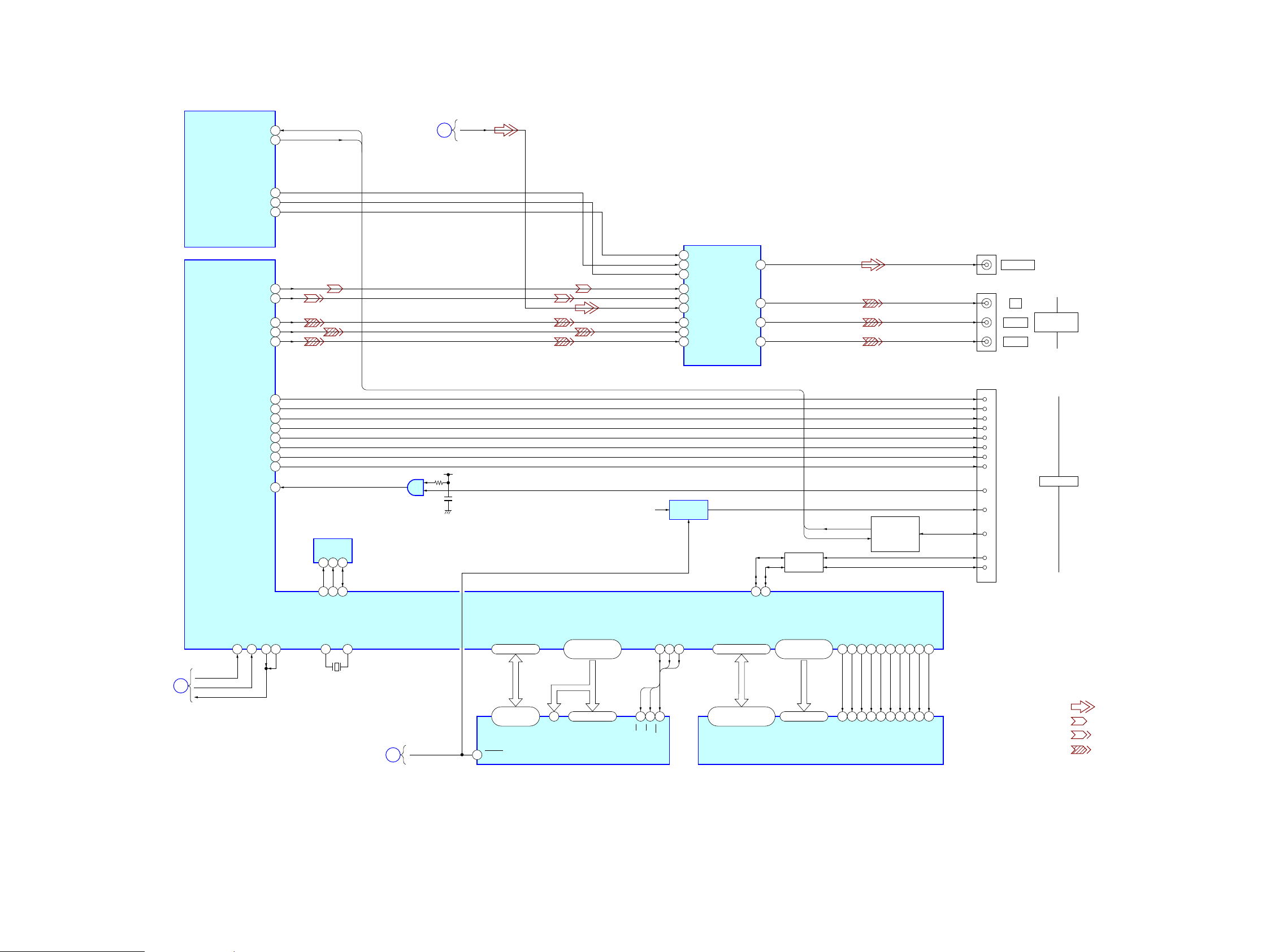
HCD-JZ8888K
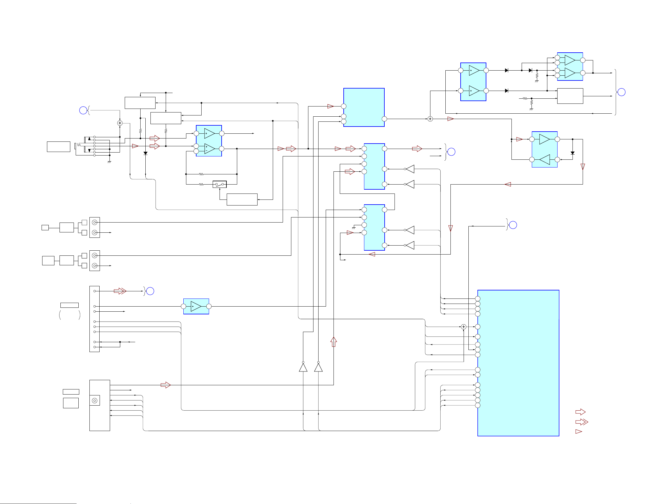
5-2. BLOCK DIAGRAM – VIDEO Section –
IC503 (2/6)
SYSTEM CONTROL
CEC_RX_IN
CEC_TX_OUT
6
26
82V_SEL1
81V_SEL0
83V_SEL2
191Y
189C
185Y/G
183B/Cb/Pb
182R/Cr/Pr
180TX2P
179TX2N
177TX1P
176TX1N
174TX0P
173TX0N
171TCKP
170TCKN
162HTPLG
CEC_RX_IN
CEC_TX_OUT
IC1103
EEPROM
WFEEWP
SCL6SDA
7
AUDIO
SECTION
VIDEO
B
(Page 23)
V_SEL1
V_SEL0
V_SEL2
IC4002
VIDEO DRIVER
5YC MIX
13 MUTE2
3MUTE1
6YIN
2CIN
4 CVBSIN
10 CYIN
12 CBIN
14 CRIN
+3.3V
2
4
IC1705
BUFFER
5
1
+6V
IC1707
+5V REG.
23CVBSOUT
20CYOUT
18CbOUT
16CrOUT
Q1701
LEVEL SHIFT
VOUT
CYOUT
CBOUT
CROUT
CEC_RX_IN
CEC_TX_OUT
Q9724,9726,
Q9728,9729
CEC RX/TX
INTERFACE
J4001 (1/2)
J4000
CN1701
1
3
4
6
7
9
10
12
19
18
13
15
16
VIDEO OUT
Y
PB/CB
PR/CR
TMDS DATA2 +
TMDS DATA2 –
TMDS DATA1 +
TMDS DATA1 –
TMDS DATA0 +
TMDS DATA0 –
TMDS CLOCK +
TMDS CLOCK –
HPD
+5V POWER
CEC
SCL
SDA
COMPONENT
VIDEO OUT
HDMI OUT
HCD-JZ8888K
AUDIO
SECTION
(Page 23)
112 101 102
SCL
SDA
SCORE/DIR_XSTATE
XVOICE/DIR_CSFLAG
Rt/DIR_DI
198
SCORE
XVOICE
D
MUSIC
Lt/DIR_DO
214
230
231 239 238
XTALI
X1101
27MHz
XTALO
RF
SECTION
IC1101 (2/2)
DVD SYSTEM CONTROL, DSP
XSYSRST
C
12
HD0–HD7
79,80,82–86,89
HD0–HD7
HD0–HD7
29,31,33,35,
38,40,42,44
DQ0–DQ7
RESET
HA0–HA21
56–64,67–75,77,
A0–A21
A0
25–16,10–1,48
A0–A19,NCDQ15/A-1
IC1102
FLASH ROM
87,91,92
A1–A21
XRD
XROMCS
76
XWR
11OE28CE2645
XWR66XRD78XROMCS
2,4,5,7,8,10,11,13,42,
WE
44,45,47,48,50,51,53
161
RD0–RD15
117–113,119–129
RD0–RD15
159
DDC_DA
DDC_CLK
RA0–RA11
139–141,143,144
149–155
22–26,29–35
A0–A11
IC1104
SDRAM
BA0
138
137
135
133
136
146
147
132
111
134
CKE
DQM1
DQM0
_CAS
_RAS
_RWE
_RCS
DRCLK
BA1
v SIGNAL PATH
: VIDEO
20
/CS
/WE
BA121BA0
CLK
/CAS17/RAS
CLKE
LDQM
UDQM
: Y
: CHROMA
37
39
15
18
16
19
38
: COMPONENT VIDEO
(Page 21)
2222
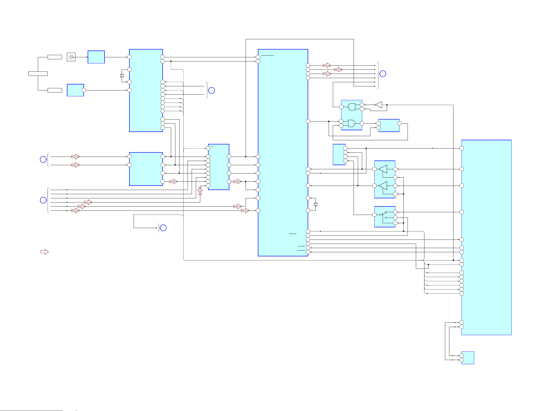
5-3. BLOCK DIAGRAM – AUDIO Section –
Q5007,5009,5012
MIC DC SWITCH
PLUG_DET
MO/ST_DET
Q5004,5005,5011
MIC DC SWITCH
D5008
(Page 25)
J5000
AUDIO IN/MIC/
A.CAL MIC
AMP
SECTION
F
PLUG_DET
SW3.3V
3 1
5
6
IC5003
MIC AMP
Q5010
7
F-AUDIO (R)
F-AUDIO (L)/MIC1
R-CH
DC_CONT
GAIN_CONT
IC4008
ELECTRONIC VOLUME
1
VIN1
4
DATA
5
CLK
INPUT SELECT
5 3
2
4
1
OUT1
IC4007
Y1 Y
Y2
Y3
Y0
HCD-JZ8888K
IC4202
ALC
SCORE DETECT
2
3
6
5
Q4201,4202
SCORE
DETECT
8
4
D4008
1
SCORE
7
VIDEO
XVOICE
D
SECTION
(Page 22)
MUSIC
IC4201
AF AMP
A+9V
D4203,4204
2
6
IC4010
ALC EQ AMP
5
MIC1+2
2
L-IN
R-IN
R-CH
Q4012
10
A
Q4011
9
B
ASEL0
ASEL1
E
SECTION
(Page 24)
3
MUSIC
DSP
7
D4201
D4202
1
TV
SAT/
CABLE
AUDIO
IN
AUDIO
IN
CN451
DMPORT
DIGITAL
MEDIA PORT
ANTENNA
75Ω FM
COAXIAL
J4001(2/2)
L
R
L
R
J4002
17
13
14
5
6
7
2
4
TU4001
FM
TUNER
PAC K
VIDEO
LCH
RCH
RXD
TXD
DET
VBUS (5V)
VIDEO 5V
R-CH
R-CH
L-CH
R-CH
TUNED
DI
DO
CK
CE
VIDEO
R-CH
VIDEO 5V
(DMPOART)
R-CH
B
(Page 22)
VIDEO
SECTION
DMP_TXD
DMP_RXD
DMP_DET
IC451
DMPOART
AUDIO AMP
3 1
Q5006,5008
MIC GAIN CONTROL
IC4005
INPUT SELECT
5 3
Y1 Y
2
Y2
4
Y3
10
A
1
Y0
9
B
R-CH
Q4013Q4014
Q4010
Q4009
DMP_DET
ASEL2
ASEL3
ASEL0
ASEL1
ASEL2
ASEL3
PLUG_DET
MO/ST_DET
GAIN_CONT
DC_CONT
DMP_TXD
DMP_RXD
TUNED
DI
DO
CK
CE
DSP_MASTER
IO_CE/ASEL0
84
IO_RESET/ASEL1
85
IO_DI/ASEL2
86
IO_DO/ASEL3
87
JACK1/JACK2/S-ART DET
65
MONO/ST_DET
90
MIC_GAIN
43
A.CAL MIC LEVEL/DSP_MASTER
91
DC_CONT
42
DMP_TX_OUT
35
DMP_RX_IN
36
TUNED
80
ST_DI/MIC_DATA
77
ST_DO
78
ST_CLK/MIC_CLK
79
ST_CE
76
DSP
G
SECTION
(Page 24)
IC503 (3/6)
SYSTEM CONTROL
R-ch is omitted due to same as L-ch.
SIGNAL PATH
: TUNER
DI
CK
: VIDEO
: MIC
HCD-JZ8888K
2323
HCD-JZ8888K
5-4. BLOCK DIAGRAM – DSP Section –
TV DIGITAL IN
AUDIO
SECTION
(Page 23)
RF
SECTION
(Page 21)
COAXIAL
OPTICAL
L-IN
E
R-IN
ACLK
ALRCK
ABCK
AMP_D00
A
AMP_D01
AMP_D02
v SIGNAL PATH
: TUNER
J501
IC502
OPTICAL
RECEIVER
OUT
IC501
WAVE
SHAPE
X301
24.576MHz
IC304
DIR
DIN2 (I)
5
(COAX)
XOUT (O)
21
XIN (I)
22
DIN (I)
42
(OPT)
13 VINL 14 4A
14 VINR
AUDIO (O)
DATA (O)
XMODE (I)
DO (O)
ERROR (O)
CSFLAG (O)
XSTATE (O)
BCK (O)
LRCK (O)
CKOUT (O)
IC303
A/D CONVERTER
DSP_MASTER
CL (I)
CE (I)
DI (I)
SCKI
LRCK
BCK
DOUT
24
16
DIR_ZERO
DIR_RST
48
DIR_CLK
38
DIR_CE
37
DIR_DIN
36
DIR_DO
35
DIR_ERR
34
CSFLAG
25
DIR_XSTATE
17
14
15
13
6
7
8
9
DSP_MASTER
AUDIO
G
SECTION
SI_A
DIR_CLK
DIR_DIN
SACD_SEL
H
SACD SELECT
1A/B
13 4B
11 3 A
10 3B
52A
62B
21A
31B
(Page 23)
AMP
SECTION
(Page 25)
IC306
4Y
3Y
2Y
1Y
SI_C
SI_D
IC700
DSP
NONAUDIO FLAG2
97
DSPIA DAI_P11
78
SI_B
DPFSCK DAI_P20
94
DPLRCK DAI_P18
88
DPBCK DAI_P19
89
LPCM FL/FR
79
DPSIB DAI_P12
LPCM SBL/SBR
82
DPSIE DAI_P15
LPCM SL/SR
80
DPSIC DAI_P13
LPCM C/SW
81
DPSID DAI_P14
12
LRCK
9
BCK
7
4
FL/FR DPSOA DAI_P6
SL/SR DPSOB DAI_P7
C/SW DPSOC DAI_P8
DPDVBCK DAI_P17
DPDVRCK DAI_P16
MOSI
MISO
SPICLK
CLKIN
XTAL
SPI_MAS DAI_P5
SF_CE FLAG3
FLAG0 INT_REQ
FLAG1 DIR_ERR
SPIDS
RESET
64
65
70
87
AND GATE
7
86
IC706
EEPROM
127
126
125
142
X700
25MHz
143
63
98
15
16
122
121
SCK
2
1
2
SO
5
SI
6
1
CE
IC705
AMP_D1
AMP_D2
AMP_D3
BCKO
LRCKO
MCKO
5
6
3
AMP
J
SECTION
(Page 25)
Q700
DELAY
IC703
DATA LATCH
1
D
CLK
2
IC702
BUS BUFFER
3 5
6
IC701
DATA SELECT
5
SF_MASTER
SF_CE
DIR_XSTATE
4
Q
IC503 (4/6)
SYSTEM CONTROL
DSP_MISO
DSP_MOSI
7
2
1
1
2
6
DSP_SPICLK
DSP_SF_CE
DSP_MASTER
DIR_XSTATE
DIR_ERR
DIR_CE
DIR_DO
CSFLAG
DIR_RST
DIR_ZERO
SACD_SEL
DSP_MISO
22
DSP_MOSI
24
DSP_SPICLK
23
DSP_SF_CE
21
68
A.CAL_OUT/DSP_INTR
DSP_SPIDS
25
DSP_RESET
27
17
DIR_XSTATE
10
DIR_ERR
70
DIR_HCE/eHDMI_SEL
100
DIR_HDOUT
19
DIR_CSFLAG
11
DIR_RST
18
DIR_ZERO
69
SACD_SEL
HCD-JZ8888K
29
E2P_CLK/S-AIR_CLK
30
E2P_SDA/S-AIR_SDA
IC505
EEPROM
5
SDA
6
SCL
2424
5-5. BLOCK DIAGRAM – AMP Section –
DSP
SECTION
(Page 24)
DSP
SECTION
(Page 24)
AUDIO
SECTION
(Page 23)
IC503 (5/6)
SYSTEM CONTROL
S_AIR_RST/C_SWR_SEL
S_AIR_ADC_SEL/DRIVER_C_EN
HP_MUTE/S_AIR_Rcv_SEL
DIR_CLK SHIFT
DIR_DIN SCDT
H
AMP_D1
AMP_D2
AMP_D3
J
BCKO
LRCKO
MCKO
IC3905
C/SWR SELECT
6
3
1 7
PLUG_DET
F
37
38
71
1DAMP_SCDT/DIR_DIN
2DAMP_SHIFT/DIR_CLK
59DAMP LAT1
60DAMP LAT2
61DAMP LAT3
57DAMP INIT
58SOFT MUTE
55OVERFLOW1
56OVERFLOW2
54DRIVE RST(EN)
67SD(DIAG)/PVDD_DET
66DC_DET
2
5
C_SWR_SEL
C_SWR_SEL
EN_C
HPMUTE
SCDT
SHIFT
LAT1
LAT2
LAT3
NS_INIT
SOFTMUTE
OVF1
OVF2
SD_PVDD_DET
DC-DET
AMP_D3
MCK0
BCK0
LRCK0
OVF2
SCDT
SHIFT
LAT3
NS_INIT
SOFTMUTE
AMP_D1
MCK0
BCK0
LRCK0
OVF1
SCDT
SHIFT
LAT1
NS_INIT
SOFTMUTE
AMP_D2
MCK0
BCK0
LRCK0
SCDT
SHIFT
LAT2
NS_INIT
SOFTMUTE
EN
IC3030
S-MASTER PROCESSOR
31
DATA
36 XFSIIN
30 BCK
29 LRCK
25 OVF FLAGL
24 OVF FLAGR
21 SCDT
22 SCSHIFT
23 SCLATCH
27 INIT
19 SOFTMUTE
IC3010
S-MASTER PROCESSOR
31
DATA
36 XFSIIN
30 BCK
29 LRCK
25 OVF FLAGL
24 OVF FLAGR
21 SCDT
22 SCSHIFT
23 SCLATCH
27 INIT
19 SOFTMUTE
IC3020
S-MASTER PROCESSOR
DATA
31
36 XFSIIN
30 BCK
29 LRCK
25 OVF FLAGL
21 SCDT
22 SCSHIFT
23 SCLATCH
27 INIT
19 SOFTMUTE
24 OVF FLAGR
Q3552 – 3555
B+ DOWN PROTECT
Q502,503
BUFFER
OUTR1(+)
OUTR1(+)
HCD-JZ8888K
IC3001
HEADPHONE AMP
3
2
5
IC3904
Y
A/B
Y
A/B
C/SWR SELECT
1
A
2
B
5
6
C/SWR SELECT
1
A
2
B
5
6
+31V
K
A/B
IC3902
A/B
POWER
SECTION
5
6
5
6
C_SWR_SELECT
Y
Y
SW
6OUTR1(+)
IC3903
SW
6OUTR2(–)
9OUTL1(–)
11OUTL2(+)
38FS0I
48XFS0IN
43HPOUTL2
45HPOUTL1
39HPOUTR2
41HPOUTR1
6
4OUTR2(–)
11OUTL1(+)
9OUTL2(–)
37FS0CKOUT
38FS0I
48XFS0IN
14XFS0OUT
6
4OUTR2(–)
11OUTL1(+)
9OUTL2(–)
38FS0I
48XFS0IN
14XFS0OUT
C
C
D3552
EN
C/SWR SELECT
1
A
2
B
IC3901
C/SWR SELECT
1
A
2
B
HP
HP
HP
HP
FR
FR
FL
FL
IC3051
CLOCK
OSCILLATOR
X3051
49.1MHZ
SR
SR
SL
SL
6
EN_C
1
7
(Page 26)
L
R
IC3500
DIGITAL POWER AMP
16 PWM_B
8 PWM_A
76/RESET
IC3400
DIGITAL POWER AMP
16 PWM_B
8 PWM_A
7
/RESET
IC3300
DIGITAL POWER AMP
16 PWM_B
8 PWM_A
76/RESET
IC3100
DIGITAL POWER AMP
16 PWM_B
8 PWM_A
7
/RESET
IC3150
DIGITAL POWER AMP
8 PWM_A
16 PWM_B
76/RESET
IC3200
DIGITAL POWER AMP
16 PWM_B
8 PWM_A
7
/RESET
IC3250
DIGITAL POWER AMP
8 PWM_A
16 PWM_B
7
/RESET
Q3551
DC BALANCE
PROTECT
OUT_B
OUT_A
SD
OUT_B
OUT_A
SD
6
OUT_B
OUT_A
SD
OUT_B
OUT_A
SD
6
OUT_A
OUT_B
SD
OUT_B
OUT_A
SD
6
OUT_A
OUT_B
SD
6
PLUG DET
HPMUTE
31
33
34
36
31
33
34
36
31
33
34
36
31
33
34
36
34
36
31
33
31
33
34
36
34
36
31
33
Q3081
H/P MUTE
DRIVE
LPF
LPF
D3551
LPF
LPF
LPF
LPF
LPF
LPF
LPF
LPF
LPF
LPF
LPF
LPF
M+14V
Q3251,3252
DC BALANCE
DETECT
Q3301,3302
DC BALANCE
DETECT
Q3101,3102
DC BALANCE
DETECT
Q3151,3152
DC BALANCE
DETECT
Q3401,3402
DC BALANCE
DETECT
Q3202,3201
DC BALANCE
DETECT
Q3000 – 3002
FAN
DRIVE
Q3116—3119
MUTE
Q3451,3452
DC BALANCE
DETECT
TB3901
TB301
FAN3001
DC FAN
(+)
L
(–)
SUBWOOFER
(+)
L
(–)
(–)
(+)
(+)
(–)
(+)
(–)
(+)
(–)
(+)
(–)
J5001
PHONES
SPEAKER
CENTER
FRONT R
SPEAKER
FRONT L
SUR R
SUR L
v SIGNAL PATH
: TUNER
HCD-JZ8888K
2525
HCD-JZ8888K
5-6. BLOCK DIAGRAM – POWER Section –
OPERATION
. >
D5400
@/1
D5601
KEY
ILLUMINATION
D5500—5502
KEY
ILLUMINATION
E+4V
S5501
VOLUME
S5500
DIAL
S5109
N
S5400
@/1
IC506
RESET
S5103,5600
FUNCTION
S5100—5102
FUNCTION
LED DRIVER
LED DRIVER
LED DRIVER
IC5002
REMOTE
CONTROL
RECEIVER
ROTARY
SWITCH
ROTARY
SWITCH
KEY
KEY
Q5400
Q5600
Q5500
D501
Q501
RESET
SYSTEM CONTROL
94 KEY2
95 KEY1
97 KEY0
73 KEY_INT
28 LED_PWM
12 RESET
20 AC CUT
4 SIRCS_IN
IC503 (6/6)
FL_CS
T5000
DC/DC
D5000
IC5001
FL DISPLAY
DRIVER
30VEE
7FL_CLK/LED_CLK
5FL_DATA/LED_DATA
3
39P.CONT1
8CLK
7DIN
9STB
P.CONT1
RF
SECTION
(Page 21)
S2 – 16
G1 – 12
L
15
–
29
42
–
31
1LED1
2LED2
3LED3
VBUS_SW
VIDEO+5V
(DMPORT)
D5002
+3.3V-3
(IC1101)
RF+3.3V
(IC1101)
+3.3V-2
(IC1101)
+3.3V-1
(IC1101)
+1.8V
(IC1101)
USB 5V
+5V
D5001
F1
F2
CONVERTER
TRANSFORMER
ND5000
FLUORESCENT
INDICATOR
TUBE
Q5001,5002,5601
LED DRIVER
IC1105
+3.3V REG.
IC1107
+3.3V REG.
IC1708
+3.3V REG.
IC 1110
+1.8V REG.
IC509
+5V REG.
Q5000
5V (FL)
IC452
+5V REG.
IC507
+5V REG.
DC/DC
CONVERTER
D5003
MOVIE
D5004
MUSIC
D5600
REC TO USB
M+14V
M+9V
(VIDEO)
(DSP)
A12V
+9V
+5V
+6V
+1.2V
F945
+1.2V REG.
AMP
SECTION
(Page 25)
P.CONT1
M+9V
IC4009
+9V REG.
IC4003
+5V REG.
IC707
K
M+14V
12V
+31V
(DIGITAL AMP)
EN
6V
IC941
+12V REG.
Q945
B+ SWITCH
PS956
IC932
SHUNT REG.
Q943,947
POWER DOWN
DETECT
Q949,950
POWER
PROTECT
D931
D912
D916
D911
T901
MAIN
TRANSFORMER
PC901
FEED BACK
PC903
STANDBY
CONTROL
T903
SUB
TRANSFORMER
D905
D901
Q901
POWER CONTROL
D914
Q951
OVER
CURRENT
PROTECT
D906
LF901,902
FILTER
IC901
SWITCHING
REGULATOR
3D
4VCC
2GND
5FB/OLP
1 OCP/SYNC
IC921
SWITCHING
REGULATOR
7VIN
9D
F901
(AC IN)
HCD-JZ8888K
X501
5MHz
Xout
13
15
Xin
41WRITE EMP P_CONT3
P.CONT3
D3.3V
+1.8V
(D-AMP)
5V
(FL)
+3.3V
(IC5001)
LED+5V
IC3050
+1.8V REG.
IC5000
+3.3V REG.
IC510
+3.3V REG.
IC504
+5V REG.
IC508
+5V REG.
E4V
E3.3V
D503
E+4V
PS954
P.CONT3
D947
IC923
SHUNT REG.
Q930
POWER
CONTROL
D902
PC902
FEED BACK
PC904
STANDBY
CONTROL
Q922
+21V REG.
Q921
DZ904
D923
4VCC
2FB
1ZC
2626
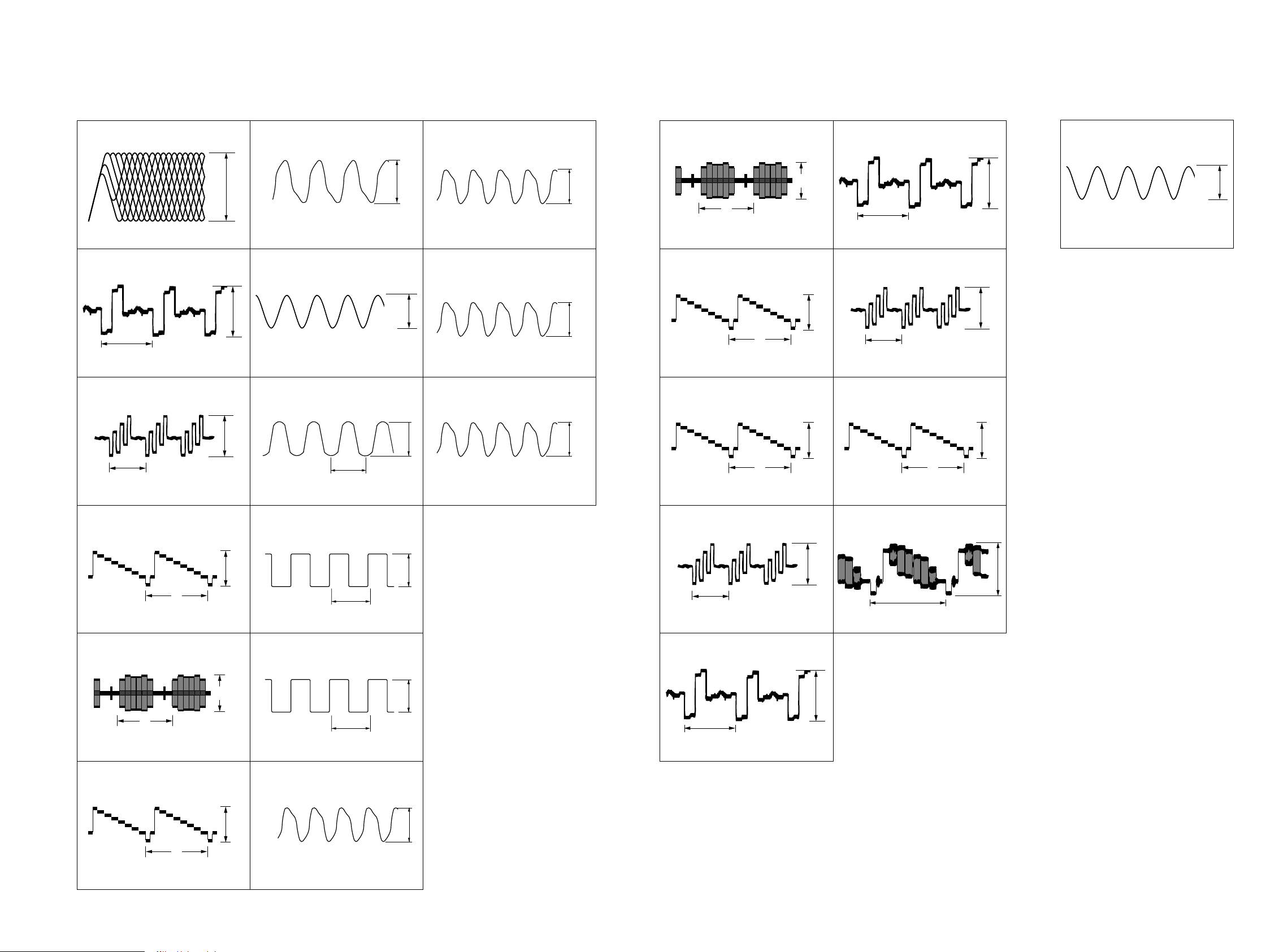
• Waveforms
HCD-JZ8888K
– MAIN Board –
1 IC1101 0 (DVDRFIP)
200 mV/DIV, 100 ns/DIV
2 IC1101 <z,x (R/Cr/Pr)
H
200 mV/DIV, 20 Ps/DIV
3 IC1101 <z,c (B/Cb/Pb)
650mVp-p
0.72Vp-p
7 IC1101 <xc, (XTALO)
27MHz
500 mV/DIV, 20 ns/DIV
8 IC503 qd (Xout)
5MHz
1 V/DIV, 100 ns/DIV
9 IC304 qd (CKOUT(O))
qd IC3051 2 (3Y)
1.6Vp-p 5Vp-p
1 V/DIV, 10 ns/DIV
49.1MHz
qf IC3010 rk (XFSOIN)
3.4Vp-p
49.1MHz
1 V/DIV, 10 ns/DIV
4.3Vp-p
qg IC3010 qf (XFSOOUT)
3.5Vp-p
– IO-COMPONENT Board –
1 IC4002 2 (Cin)
H
500 mV/DIV, 20 Ps/DIV
2 IC4002 6 (Yin)
H
500 mV/DIV, 20 Ps/DIV
3 IC4002 0 (CYin)
1Vp-p
1Vp-p
1Vp-p
6 IC4002 qh (Cr OUT)
H
500 mV/DIV, 20 Ps/DIV
7 IC4002 qk (Cb OUT)
H
500 mV/DIV, 20 Ps/DIV
8 IC4002 w; (CY OUT)
2Vp-p
1Vp-p
2Vp-p
– DSP Board –
1 IC700 <zvc (XTAL)
1.8Vp-p
25MHz
0.5 V/DIV, 20 ns/DIV
H
200 mV/DIV, 20 Ps/DIV
4 IC1101 <z,b (Y/G)
500 mV/DIV, 20 Ps/DIV
5 IC1101 <z,. (C)
H
500 mV/DIV, 20 Ps/DIV
6 IC1101 <z.z (Y)
H
0.72Vp-p
1Vp-p
1Vp-p
40.7nsec
1 V/DIV, 20 ns/DIV
0 IC304 qf (BCK(O))
163nsec
1 V/DIV, 50 ns/DIV
qa IC304 qg (LRCK(O))
10.4Psec
1 V/DIV, 5 Ps/DIV
qs IC304 wa (XOUT(O))
3.5Vp-p
3.5Vp-p
49.1MHz
1 V/DIV, 10 ns/DIV
4Vp-p
H
500 mV//DIV, 20 Ps/DIV
4 IC4002 qs (Cb in)
H
200 mV/DIV, 20 Ps/DIV
5 IC4002 qf (Cr in)
H
200 mV/DIV, 20 Ps/DIV
H
1 V/DIV, 20 Ps/DIV
9 IC4002 wd (CVBS OUT)
2.6Vp-p
0.72Vp-p
H
1 V/DIV, 20 Ps/DIV
0.72Vp-p
500 mV/DIV, 20 Ps/DIV
HCD-JZ8888K
1Vp-p
H
1 V/DIV, 20 ns/DIV
24.576MHz
4Vp-p
2727
HCD-JZ8888K
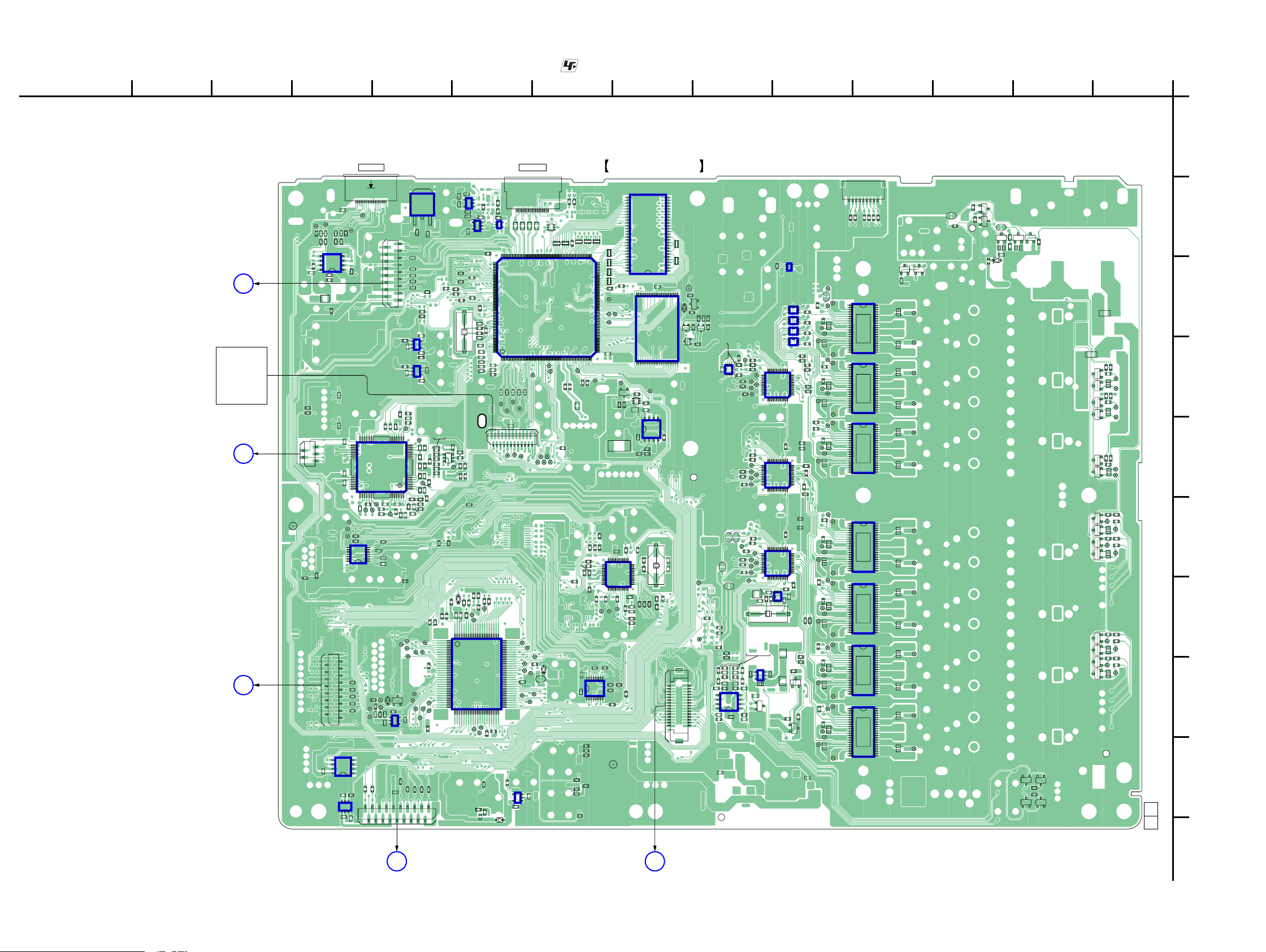
5-7. PRINTED WIRING BOARD – MAIN Section (1/2) –
CL327
R453
C457
R1246
R1247
2
4
CN1202
R328
IO-COMPONENT
BOARD
CN4003
(Page 40)
(KHM-313CAA)
IO-COMPONENT
K
DVD DRIVE
(1/2)
OPTICAL
( )
PICK-UP
D
MS-203
BOARD
CN001
(Page 29)
J
BOARD
CN4006
(Page 40)
(17P)
CN472
(17P)
CN503
• See page 20 for Circuit Boards Location.
CN451 CN1701
DMPORT HDMI OUT
IC1707
C1727
C1729
3
C1730
54
1
C1734
R1757
C1733
C1732
45
C1731
IC1708
R1159
R1160
R1161
R2187
R1146
R1183
R1184
R1185
C1153
X1101
C1152
C1148
C1147
C1139
C1138
C1137
C1135
R1114
C1113
R1123
R1107
R1124
Q1102
CL2103
R1109
R1110
R346
R344
R347
R531
R535
D501
R537
R540
R543
R532
R538
R539
CL529
CL528
R544
C514
C515
100 81
180
13
13
R1219
C1210
R1224
I
R2135
R1212
FB2124
FB2125
FB2122
FB2121
FB2120
C1186
C1195
C1208
R1210
C1203
R1215
R1214
JL510
C1198
C1211
JL506
O
C1183
R2116
IC1105
45
C1182
R1151
C1193
45
R1121
R1120
R1118
R1115
R1113
R1112
R1216
R1204
R1207
C1206
R1209
CL1201
C1205
R1208
R1225
R1220
R546
R547
R564
IC503
JL518
JL526
JL527
30 51
JL528
JL520
JL525
R592
R558
R570
R571
1
2
JL524
JL522
JL523
R621
R626
R620
JL453
R465
R451
L451
1
5
IC504
JL451
C452
C453
R452
IC451
85
R327
16
2
IC505
C526
C451
C462
C461
R456
14
C456
R454
R462
C1222
C1221
C1223
CL304
CL348
CL349
17
CN503
1
58
C520 R569
46
C516
18
JL452
R466
JL454
R457
R460
C1219
C1224
C1215
R343
R345
14 8
IC303
R514
R516
R518
R520
R523
JL532
JL531
14
13
C521
CN451
24
2536
IC1201
37
R1233
CL1208
17
R596
R598
R552
19
18
CL1207
R553
C1214
CL1206
R1230
C523
R1228
R1231
R348
C310
C309
C308
JL530
JL529
R597
C525
IC506
17
16
CN472
2
1
R1186
R1192
C1192
IC1107
R1222
R1227
C1213
13
48
C1212
R1223
CL1213
R1221
R333
JL507
JL508
JL509
JL517
Q501
D502
EB
R599
C524
R554
C522
CN507
(19P)
CN507
I
(Page 47)
IC1110
R2111
R2112
C1184
CL1205
CL1204
12
1
R1206
R1226
C1233
C1209
JL511
JL519
C527
R555
FL-JACK
BOARD
CN5001
• : Uses unleaded solder.
MAIN BOARD (SIDE A)
CN1701
R2115
CL2101
CL1121
C1136
R394
R407R408
RB1110
RB1112
R337
CL343
R405 R406
R384
RB1109
RB1113
R1156
JL1160
CL2102
Q1103
IC2101
R2191
C330
IC304
1
CL345
CL344
R356
JL471
CL2109
EB
R1116
R338
R1108
R395
C321
R340
R1117
FB2102
2536
12
C318
R574
2854
IC1104
IC1102
1
Q1101
85
C2103
14
R2192
R372
R370
24
R371
13
R342
R366
C319
R330
R341
3
1
R2101
193
R1752
R1742
C1725
13
45
IC1705
19
R1747
Q1701
64
RB1114
R1748
31
RB1103
RB1111
RB1104
R2114
RB1115
129192
128
1
L1701
L1702
L1703
L1704
IC1101
R2168
R1142
R2167
256
164
CL1116
1
2
R533
R534
JL501
R627
IC508
R622
D505
C1133
C1132
R1136
R577
CL1115
5031
C1120
C1101
CN1101
R618
C1121
CL1112
JL505
JL512
C533
C1122
CL1118
CL1114
JL502
C517
JL516
45
C1123
JL513
CL1117
CL1113
CL1101
C1124
23
JL503
R556
JL521
13
CL1105
CL1108
24
R2110
CL1302
CL1303
CL1301
CL1304
CL1305
JL504
D503
SL501
JL515
C542
65
CL1110
CL2107
R2127
R2128
R2121
R2123
L2101
R398
R397
R396
R364
37
R361
R362
R391
R390
R358
C332
16
18
C328
48
R336
9
IC306
R619
R617
R616
R625
R613
R610
R611
R615
R1111
C2101
R2193
R2194
R367
N
C1110
CL2108
X301
R368
R374
27
RB1106
RB1105
1
2548
D9712
R9935
Q9728
EB
Q9724
24
R2195
C327
C326
TP3006
R369
JL3062
29
CN305
1
DSP
BOARD
CN701
(Page 42)
CL1702
R9945
EB
EB
R9941
EB
LP301
30
IC3001
2
Q9729
C9972
R9929
R9934
R9928
Q9726
R9924
IC3905
R411
R3067
R3068
C3092
C3083
R3916
R3915
R3092
R3088
C544
LP501
C3919
SL3005
SL3006
R3076
R3074
R3075
R3922
85
1
4
TP3229
R3034
R3035
TP3231
R3037
TP3022
TP3129
R3023
R3024
TP3131
R3026
SL3003
SL3004
TP3024
R3012
TP3029
R3014
R3015
TP3002
R3017
14
85
C3008
TP3005
TP3032
TP3136
R3013
R3011
TP3036
TP3015
R3053
L3054
C3060
R3091 R3093
C3085 C3086
R3087 R3089
C3087 C3088
R3098 R3099
IC3050
R3094
R3090
C3055
C3093
R3086
C3084R3085
IC3903
IC3904
IC3901
IC3902
R3033
R3031
R3032
TP3230
TP3236
R3021
R3022
TP3130
IC3010
TP3026
TP3030
IC3051
C3059
R3052
X3051
45
C3052
R3047
EB
R505
IC501
24
2536
37
IC3030
R3057
24
2536
37
IC3020
24
2536
37
58
14
C3053
13
Q3081
L3053
L3051
R624
14
14
14
14
R3401
R3402
13
112
48
13
112
48
R3055
13
112
48
C3058
R3050
C3057
Q502
R3502
R3501
R3044
R3042
R3041
R3101
R3102
EB
R3043
R623
EB
R3054
R3251
R3201
C3003
85
85
85
85
R3301
R3302
R3304
R3908
JL3024
JL3036
R628
Q503
R3920
R3921
R3918
R3919
JL3042
R3152
R3202
JL3023
JL3029
JL3035
JL3041
R3252
R3254
JL3107
JL3110
R3151
JL3113
JL3116
TP3410
R3504
R3154
JL3047
JL3018
R3204
R3104
R3507
JL3048
R3404
R3407
JL3112
JL3013
R3307
JL3019
R3257
R3207
JL3030
R3157
R3107
JL3060
TP3510
TP3311
TP3250
TP3150
TP3110
C3926
C3925
C3924
C3922 C3923
C3920 C3921
SL3002
JL3098
JL3101
JL3104
JL3022
TP3210
JL3043
CN508
19
R605
R606
R607
R614
JL3046
1
C3504
22
JL3049
JL3011
1
C3404
22
JL3014
JL3017
1
C3304
IC3300 IC3500IC3400
22
1
C3254
IC3250IC3100 IC3150 IC3200
22
JL3025
1
JL3028
C3204
22
JL3031
JL3034
1
C3154
22
JL3037
JL3040
1
C3104
22
1234567891011121314
A
SL3007
R3559
EB
Q3554
SL3001
R3563
EB
R603
R604
Q3001 Q3002
EBEB
R3001
44
C3513
23
44
C3413
C3408
23
44
C3313 C3508
C3308
23
44
C3263
C3258
23
44
C3213
C3208
23
44
C3163
C3158
23
44
C3113
C3108
23
R3561
JL3045
JL3050
JL3010
JL3015
JL3016
JL3020
JL3021
JL3026JL3027
JL3032
JL3033
JL3038JL3039
JL3044
LP3000
Q3553
C3556
R3562
R3558
D3552
Q3555
R3552
R3556
Q3552
C3553
EBEB
Q3119
Q3551
EB
R3554
R3903
R3904
R3576
R3575
EBEB
R3577
JL3385
C3429
JL3386
Q3451 Q3452
R3275
R3276
EB
R3277
Q3251
JL3086
EBEBEBEBEBEBEBEBEBEBEB
C3129
JL3085
Q3252
R3325
R3326
Q3301Q3302
R3327
JL3052
JL3051
C3128
R3426
R3427
JL3053
R3425
JL3054
C3126
R3226
R3227
R3225
Q3201Q3202 Q3401Q3402
JL3055
JL3056
C3127
R3126
R3127
JL3058
Q3101Q3102Q3151Q3152
R3125
JL3057
C3124
R3176
R3177
R3175
JL3059
JL3087
C3125
LP3001
Q3117
BEBE
R3186
R3185
EB
EB
Q3116Q3118
1-878-150-
B
C
D
E
F
G
H
I
11
(11)
J
HCD-JZ8888K
2828
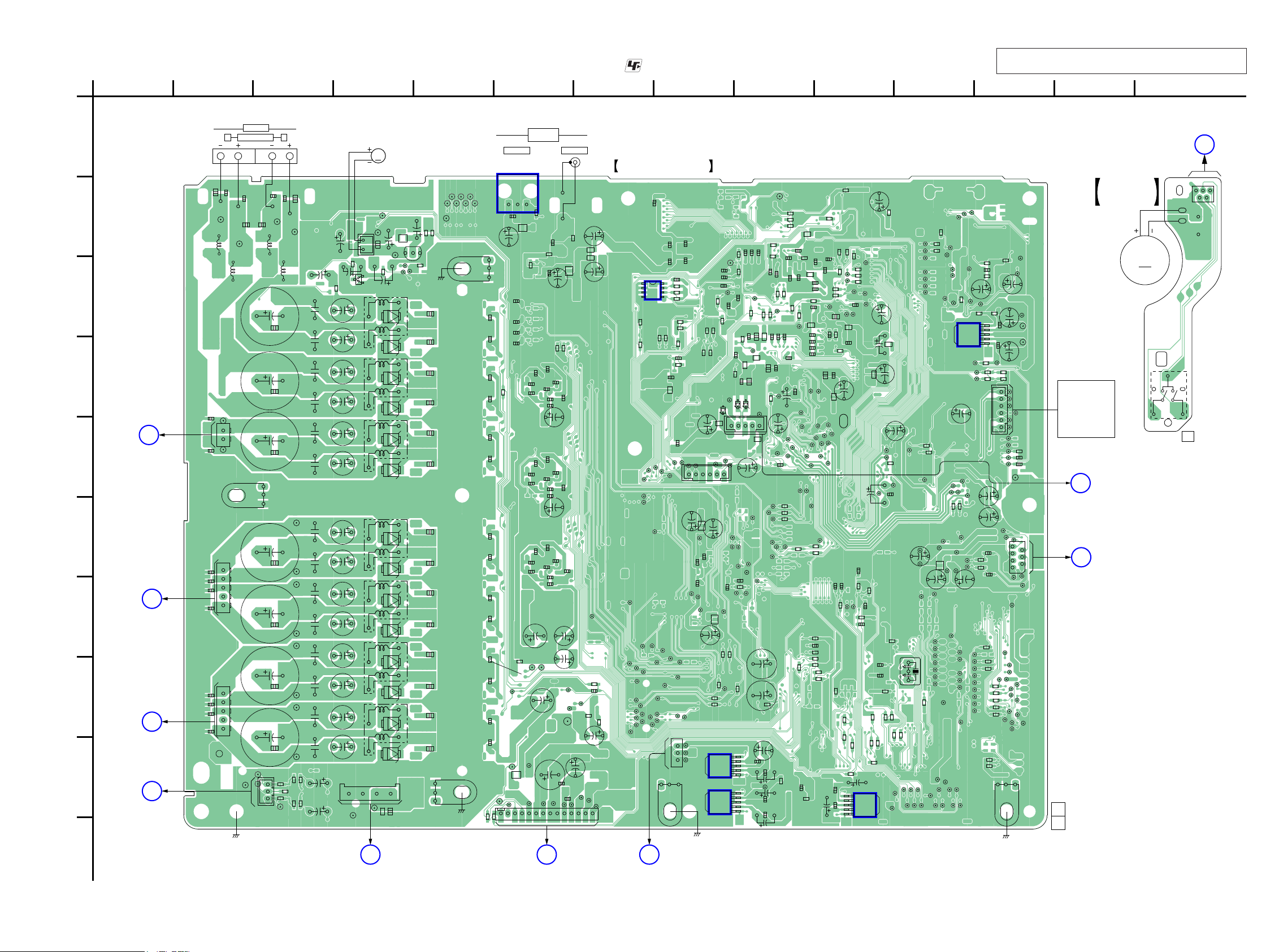
5-8. PRINTED WIRING BOARDS – MAIN Section (2/2) –
• See page 20 for Circuit Boards Location.
• : Uses unleaded solder.
HCD-JZ8888K
When IC1103 on the Main board is damaged, exchange the
new Main board for the Main board which IC damaged.
A
B
C
D
E
F
G
H
I
J
1
SP
BOARD
CN304
(Page 51)
SP
BOARD
CN304
(Page 51)
SP
BOARD
CN303
(Page 51)
FL-JACK
BOARD
CN5005
(Page 47)
B
C
A
E
234567891011121314
(Page 28)
MAIN BOARD
CN1202
D
1
5
CN001
42
12
SUBWOOFER
R
C3902
C3912
TP3308
L3902
TP3307
L3901
TP3305
C3373
2
CN3300
1
C3372
TP3306
EB3004
C3423
C3422
C3323
C3322
C3173
C3172
C3123
C3122
CN3200
15
5
CN3100
1
LP3001
(CHASSIS)
TB3901
SPEAKER
C3901
C3911 C3914
TP3083
JL3005
TP3082
L
C3904
C3903
TP3310
TP3309
L3904
L3903
C3516
C3517
C3416
C3417
C3316
C3317
TP3304
C3266
C3267
C3216
C3217
C3166
C3167
C3116
C3117
FB3109
FB3108
FB3107
CN3001
13
TP3081
TP3303
TP3302
TP3301
TP3104
TP3103
TP3102
TP3101
R3184
R3183
C3913
R3192
R3191
C3414 C3415
C3314 C3315 C3514 C3515
C3264 C3265
C3214 C3215
C3164 C3165
C3114 C3115
RED
BLK
C3561
C3552
C3082
C3081
12
C3551
R3551
D3551
R3553
C3512
L3501
C3509
C3412
L3401
C3409
C3312
L3301
C3309
C3262
C3259
C3212
L3201 L3202L3101 L3102
C3209
C3162
C3159
C3112
C3109
CN904
14
TP3054
G
FAN3001
M
TP3007
TP3000
C3002
CN3000
TP3001
R3002
C3001
D4501 D4502
D4402
D4401
D4301 D4302
D4251 D4252
D4202
D4201
D4152
D4151
D4111 D4112
TP3053
R3051
POWER
BOARD
CN904
(Page 53)
C3000
FAN
C3051
JL3096
L3000
EC
JL3002
D3302
JL3001
C3005
B
Q3000
R3006
R3004
C3506
C3507
C3406
C3407
C3306
C3307
C3256
C3257
C3206
C3207
C3156
C3157
C3106
C3107
CL548
CL555
R3003
(CHASSIS)
CL549
CL550
EB3002
(CHASSIS)
CL551
CL552
EB3001
CL553
CL554
C3503
C3505
C3403
C3405
C3303C3305
C3253C3255
C3203
C3205
C3153C3155
C3103
C3105
R630
C505
R629
1
IC502
IC502
IGO
C504
C3917
C3918
C3915
C3916
R3907
TP3004
L3052
CL558
CL556
R3040
CL557
L501
C3033
C3032
C3023
C3022
DIGITAL IN
R504
C3039
C3040
C3024
C3029
C3030
C3014
C3013
C3012
C3056
JL534
CL567
CL559
TV
R506
C3034
C3038
C3028
C3018
JL535
C3091
CN509
F
C501
R501
C508
C507
C3035
C3036
C3031
C3025
C3026
C3021
C3015
C3016
C3019
C3020
C553
CL560
(Page 53)
COAXIALOPTICAL
R3060
R3059
C3037
C3027
C3017
C3011
C3054
TP3003
JL3003
JL533
C551
C550
CL561
CL562
POWER
BOARD
CN906
L502
JL3004
CL563
J501
R502
R3096
C552
CL564
MAIN BOARD (SIDE B)
C1197
C1190
C1177
C3090
CL565
FB1108
FB1106
CL363
14
R3065
C3071
CL566
R3095
CL389
CL379
CL385
CL359
CL376
CL395
R9922
R9918
CL375
CL373
CL393
1
4
IC1103
CL570
CL575
CL573
CL576
CL360
CL358
CL381
CL377
CL382
CL387
CL390
CL391
CL396
O
CL577
C1181
C1180
C1191
C1179
C2130
R1135
R1193
58
R1191
R2151
R2150
R1105
R1106
R2160
C2100
R1198
C1102
FB1111
C2102
CL572
CL571
JL1108
JL1107
CL574
CL569
16
CN1105
C315
CL370
C325
CL346
CL380
CL374
CL357
CL372
CL384
CL383
CL378
CL386
CL394
CL388
CL392
1
CL397
CL398
CN304
CL399
3
ET301
(CHASSIS)
DSP
BOARD
CN700
C2119
C1158
C1160
R1154
C1155
R2156
R2158
R2152
R2157
R2159
D2101
15
C2112
FB2104
JL1111
JL1110
L303
C331
CL369
CL367
C329
C317
C323
CL341
CL326
CL347
L301
C304
R385
R404
CL371
R383
R382
IC510
66
15
15
IC507
CL2120
JL1109
CL353
R386
CL1123
C1127
R2155
JL1112
CL364
R1133
FB1116
C2116
D2102
CN2101
FB2105
C1119
CL366
R357
R1140
C1144
R1103
C316
R334
C1164
CL1109
D2103
CL578
C538
C529
C540
C532
C2114
FB1117
CL356
CL352
CL365
C1162
C2117
CL2121
R1155
C2115
C536
C528
R572
CL324
C1176
JL2113
CL368
C537
CL320
R1781
R1782
C1174
R1171
FB1115
R1101
CL323
CL325
CL321
CL322
CL568
C2503
(LOADING)
DVD DRIVE
(2/2)
MOTOR
H
(Page 51)
IO-COMPONENT
M
MS-203
BOARD
M001
S001
USB
BOARD
CN5201
BOARD
CN4011
(Page 40)
M
(CHUCK/TRAY DETECT)
1-861-327-
R1137
C1154
JL2118
CL302
JL2115
JL2114
CL301
FB1107
JL2110
CL471
C1163
JL2111
JL2121
JL2116
JL2108
R476
R478
R548
C554
R549
R550
R563
R2180
R2138
R560
R557
C545
R1744
C1169
C1151
C1129
JL2105
JL2107
C1161
C2108
FB1112
JL2109
CL2140
CL2123
C1159
JL2106
JL2104
C541
R2137
C510
JL2103
JL2103
R585
R1753
R1176
CL2139
CL2126
R1141
C509
R529
C546
R1132
CL2138
R559
R561
R593
R2181
C1170
FB1109
C1165
C1111
CL526
R586
C543
R1182
R1181
R2189
R1126
CL2124
CL2125
C1105
C512
R542
C511
CL527
R545
C513
15
IC509
CL2135
CL2141
C519
C518
R590
R541
C1187
C2109
FB2101
CL1107
R568
R591
R595
6
CL452
R2178
R490
JL472
R492
JL474
JL475
JL478
JL479
JL480
JL481
C1145
FB2103
C2110
C1112
CL2104
JL2102
R2129
CL1106
C1106
R581
R579
R594
R636
R567
CL547
X501
CL546
CL1203
C314
R566
CL545
CL544
CL543
CL542
CL1202
CL455
CL340
CL541
CL362
CL318
CL305
CL307
CL309
CL311
CL313
CL315
CL540
R1213
R1205
CL339
L302
C313
CL361
CL310
R582
CL538
CL539
CL537
CL453
R491
JL477
CL454
JL484
JL2124
CL342
CL338
CL317
CL534
CL536
CL535
JL473
JL476
CL458
JL482
R499
6
IC452
CL460
JL1213
JL1212
C1217
CL1211
CL1212
CL1209
R1232
R1234
CL350
CL459
CL336
C311
CL306
CL308
CL312
CL314
CL316
CL579
CL531
CL533
CL530
CL532
1-878-150-
CL451
C464
JL485
R461
15
R464
R1237
R1236
CL1210
CL337
CL335
R513
CL501
CL503
CL505
CL507
CL509
CL511
CL513
CL515
CL517
C1218
C1220
R331
R332
R508
R511
R515
R517
R519
R521
R522
CL510
JL483
R459
C463
R458
R463
CN1201
JL1210
JL1211
JL1209
JL1208
JL1207
C305
C303
CL518
R584
R583
C467
CL504
C466
CL506
6
1
CL512
CL514
JL456
CL502
CL521
R455
CL328
CL508
ET501
CL523
CL516
C465
CL522
CL525
R1239
R1238
CL330
CL524
C455
CL331
CN302
CL333
JL1206
JL1205
JL1204
JL1202
JL1201
CL520
CL329
1
C468
JL1203
7
CL519
CL456
2
6
CL457
R1243
C1226
C1225
CL461
CL334
CL332
JL455
CL462
SPINDLE/SLED
( )
(7P)
CN302
11
(11)
CL1701
R1751
R1749
R1750
FB1113
C2502
C1108
R1730
FB1118
C1172
C1109
C1175
C1156
C1171
R2185
R2184
R2179
R2103
R2104
CL2122
CL2137
C1126
C1115
C1116
C1130
C1140
C1146
C1149
C1125
C2118
C1117
C1114
JL2117
JL2120
C1118
JL2119
JL2112
JL2101
JL2122
JL2123
C1199
CL303
R484
R485
R489
R477
CL319
R573
C539
R609
C534
R612
C530
C531
(CHASSIS)
(Page 43)
HCD-JZ8888K
2929
 Loading...