

Sony HCD-H331, HCD-H331D Service Manual

HCD-H331/H331D
SERVICE MANUAL
r
HCD-H331/H331D is the tuner, deck,
CD and amplifier section in MHC-331,
MHC-D2, MHC-G33.
Photo : HCD-H331
Dolby noise reduction manufactured under license from
Dolby Laboratories Licensing Corporation.
“DOLBY” and the double-D symbol a are trademarks of
Dolby Laboratories Licensing Corporation.
CD
Section
Tape deck
Section
SPECIFICATIONS
US Model
HCD-H331/H331D
Canadian Model
E Model
Austr alian Model
HCD-H331
Model Name Using Similar Mechanism HCD-H881/H881D
CD Mechanism Type CDM38-5BD19
Base Unit Name BU-5BD19
Model Name Using Similar Mechanism NEW
Tape Transport Mechanism Type TCM-YSW47C24
AUDIO POWER SPECIFICATIONS
POWER OUTPUT AND TOTAL
HARMONIC DISTORTION :
with 6 ohm loads, both channels driven,
from 40-20kHz ; rated 100 watts per
channel minimum RMS power, with no
more then 0.9 % total harmonic distortion
from 250 milliwatts to rated output.
CD player section
System Compact disc and digital audio
system
Laser Semiconductor laser
Laser output Max 44.6µW*
*This output is the value measured at
a distance of 200 mm from the objective lens surface on the Optical
Pick-up Block with 7 mm aperture.
Wavelength 780–790 nm
Frequency response
2Hz – 20kHz (± 0.5 dB)
Signal-to-noise ratio
More than 90 dB
Dynamic range
More than 90 dB
Tuner section
FM stereo, FM/AM superheterodyne tuner
FM tuner section
Tuning range US, Canadian model :
87.5 - 108MHz (100kHz step)
EXCEPT US, Canadian model :
87.5 - 108MHz (50kHz step)
Antenna FM lead antenna
Antenna terminals
75 ohm unbalanced
Intermediate frequency
10.7 MHz
AM tuner section
Tuning range
US, Canadian model :
531-1,710kHz (with the tuning
interval set at 9 kHz)
530-1,710kHz (with the tuning
interval set at 10 kHz)
E, Argentine, Australian, Mexican
model :
531-1,602kHz (with the tuning
interval set at 9 kHz)
530-1,710kHz (with the tuning
interval set at 10 kHz)
Antenna AM loop antenna
External antenna terminals
MINI Hi-Fi COMPONENT SYSTEM
Intermediate frequency
450kHz
Amplifier section
US, Canadian model :
FTC 100W+100W (8ohm, 40-20kHz, 0.9% THD)
Continuous RMS power output
120W + 120W (8 ohm, 1kHz, 5% THD)
EXCEPT US, Canadian model :
Peak music power output
400W
Continuous RMS power output
20W + 20W (6 ohm, 1kHz, 10% THD)
Inputs
VIDEO IN (phono jacks) :
voltage 450 mV
impedance 47 kilohm
Outputs
PHONES (stereo phono jack) :
accepts headphones of 8 ohm or more
SPEAKER :
accepts impedance of 6 to 16 ohm
SUPER WOOFER :
voltage 1V, impedance 1 kilohms
(HCD-H331 only)
–Continued on page 2–
MICROFILM

TABLE OF CONTENTS
Tape player section
Recording system
Frequency response
Wow and flutter
Supplied accessories
AM loop antenna (1)
Remote RM-SC100P (1) (HCD-H331 : US, Canadian model)
Remote RM-SD25 (1) (EXCEPT HCD-H331 : US, Canadian model)
Sony SUM-3 (NS) batteries (2)
FM lead antenna (1)
Speaker cords (4)
General
Power requirements
US, Mexican model
Canadian model 70VA
Australian model 240V AC, 50/60Hz 70W
E, Argentine model
Dimensions Approx. 280x325x360 mm
Mass US, Canadian model
Design and specifications are subject to change without notice.
4-track 2-channel stereo
(DOLBY NR OFF)
60 - 13,000 Hz (±3 dB),
using Sony TYPEI cassette
60 - 14,000 Hz (±3 dB),
using Sony TYPEII cassette
±0.15% W. Peak (IEC)
0.1% W. RMS (NAB)
±0.2% W. Peak (DIN)
Destination Power requirements
120V AC,60Hz
110 - 120V/ 220 - 240V AC,
50/60Hz Adjustable with the
Voltage Selector
(111/8x127/8x141/4 in)
(w / h/ d)
incl. projecting parts and controls
Approx. 7kg (15 lb)
Other model
Approx. 9.0kg (19 lb 14 oz)
Power
consumption
70W
70W
Section Title Page
______ ____ ____
Specification .................................................................................1
1. SERVICING NOTES ........................................................... 4
2. GENERAL
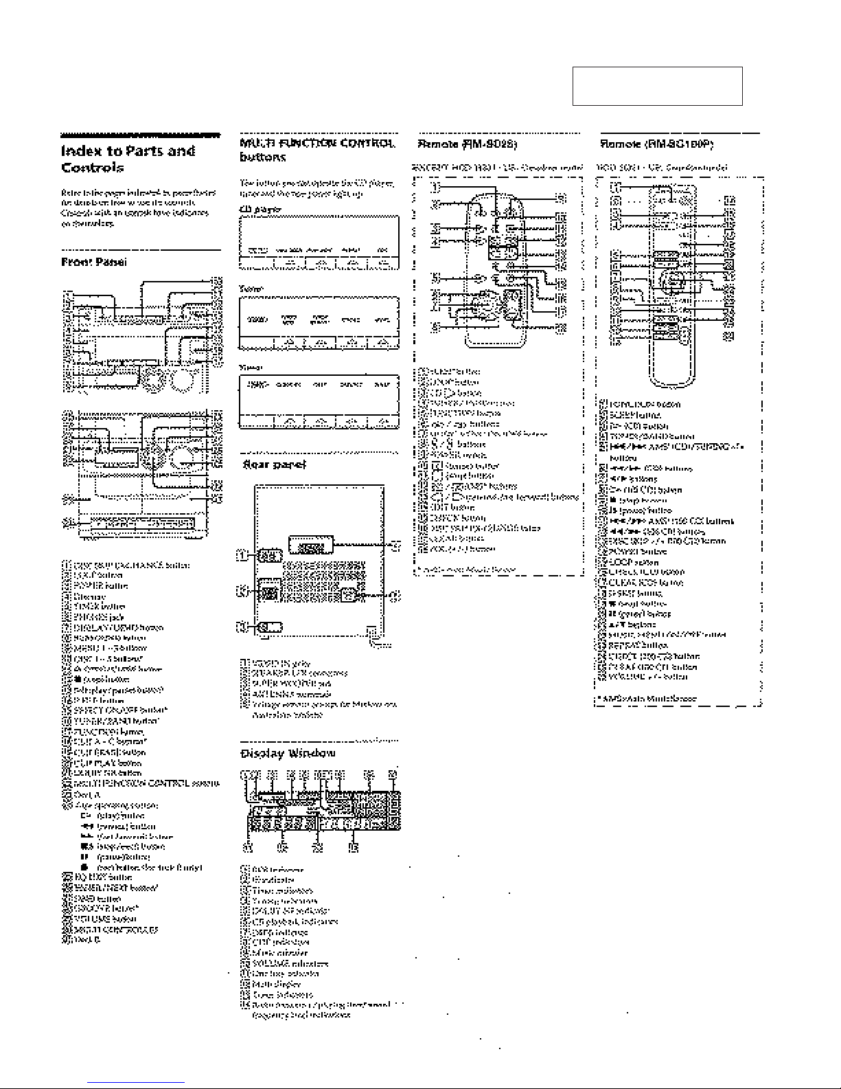
Index to Parts and Controls .................................................... 6
3. DISASSEMBLY
3-1. Front Panel Removal....................................................... 7
3-2. CD Block Removal ......................................................... 7
3-3. Lid (A)/(B) Assy, Cassette,
Mechanism Deck Block Removal................................... 8
4. MECHANICAL ADJUSTMENTS...................................... 9
5. ELECTRICAL ADJUSTMENTS ....................................... 9
6. EXPLANATION OF IC TERMINALS................................ 14
7. DIAGRAMS
7-1. Block Diagram – CD Section – ...................................... 19
7-2. Block Diagram – Main Section – ................................... 21
7-3. Circuit Board Location ................................................... 25
7-4. Printed Wiring Boards – Main Section – ........................ 26
7-5. Schematic Diagram – Main Section (2/2) –.................... 29
7-6. Schematic Diagram – Main Section (1/2) –.................... 31
7-7. Schematic Diagram – Panel Section – ............................ 36
7-8. Printed Wiring Boards – Panel Section –........................ 38
7-9. Printed Wiring Boards – BD Section –........................... 41
7-10. Schematic Diagram – BD Section – ............................. 43
7-11. IC Block Diagram ......................................................... 46
8. EXPLODED VIEWS
8-1. Chassis Section ............................................................... 48
8-2. Front Panel Section ......................................................... 49
8-3. Mechanism Section-1 ..................................................... 50
(TCM-YSW47C24)
8-4. Mechanism Section-2 ..................................................... 51
(TCM-YSW47C24)
8-5. Mechanism Section-3 ..................................................... 52
(TCM-YSW47C24)
8-6. Disc Table Assy Section (CDM38-5BD19).................... 53
8-7. CDM Chassis Section (CDM38-5BD19) ....................... 54
8-8. Base Unit Section-2 (BU-5BD19) .................................. 55
9. ELECTRICAL PARTS LIST .............................................. 56
– 2 –
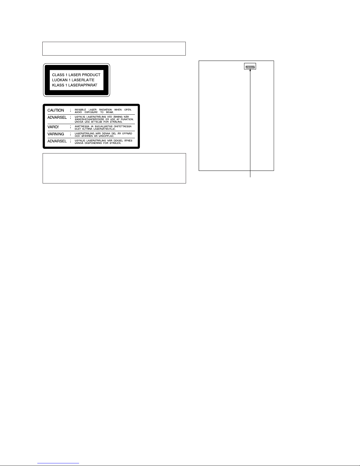
Laser component in this product is capable of emitting radiation
exceeding the limit for Class 1.
This appliance is classified as a
CLASS 1 LASER product. The
CLASS 1 LASER PRODUCT
MARKING is located on the
rear exterior.
This caution
label is located
inside the unit.
CAUTION
Use of controls or adjustments or performance of procedures other
than those specified herein may result in hazardous radiation
exposure.
SAFETY-RELATED COMPONENT WARNING!!
COMPONENTS IDENTIFIED BY MARK ! OR DOTTED LINE WITH
MARK ! ON THE SCHEMATIC DIAGRAMS AND IN THE PARTS
LIST ARE CRITICAL TO SAFE OPERATION.
REPLACE THESE COMPONENTS WITH SONY PARTS WHOSE
PART NUMBERS APPEAR AS SHOWN IN THIS MANUAL OR IN
SUPPLEMENTS PUBLISHED BY SONY.
MODEL IDENTIFICATION
– BACK PANEL–
4-979-270-0π : US model (H331)
4-979-270-1π : Canadian model
4-979-270-2π : US model (H331D)
4-979-271-0π : E model
4-979-271-1π : Australian model
4-979-271-2π : Mexican model
4-979-271-3π : Argentine model
ATTENTION AU COMPOSANT AYANT RAPPORT
LES COMPOSANTS IDENTIFIÉS PAR UNE MARQUE ! SUR LES
DIAGRAMMES SCHÉMATIQUES ET LA LISTE DES PIÈCES SONT
CRITIQUES POUR LA SÉCURITÉ DE FONCTIONNEMENT. NE
REMPLACER CES COMPOSANTS QUE PAR DES PIÈCES SONY
DONT LES NUMÉROS SONT DONNÉS DANS CE MANUEL OU
DANS LES SUPPLÉMENTS PUBLIÉS PAR SONY.
À LA SÉCURITÉ!
– 3 –
SAFETY CHECK-OUT
After correcting the original service problem, perform the following
safety check before releasing the set to the customer :
Check the antenna terminals, metal trim, "metallized" knobs, screws,
and all other exposed metal parts for AC leakage. Check leakage as
described below.
LEAKAGE TEST
The AC leakage from any exposed metal part to earth ground and
from all exposed metal parts to any exposed metal part having a return to chassis, must not exceed 0.5mA (500 microampers).
Leakage current can be measured by any one of three methods.
1. A commercial leakage tester, such as the Simpson 229 or RCA
WT-540A. Follow the manufacturers’ instructions to use these
instruments.
2. A battery-operated AC milliammeter. The Data Precision 245
digital multimeter is suitable for this job.
3. Measuring the v oltage drop across a resistor by means of a V OM
or battery-operated A C voltmeter . The “limit” indication is 0.75V,
so analog meters must have an accurate low-voltage scale. The
Simpson 250 and Sanwa SH-63Trd are examples of a passive
VOM that is suitable. Nearly all battery operated digital
multimeters that have a 2V AC range are suitable. (See Fig. A)
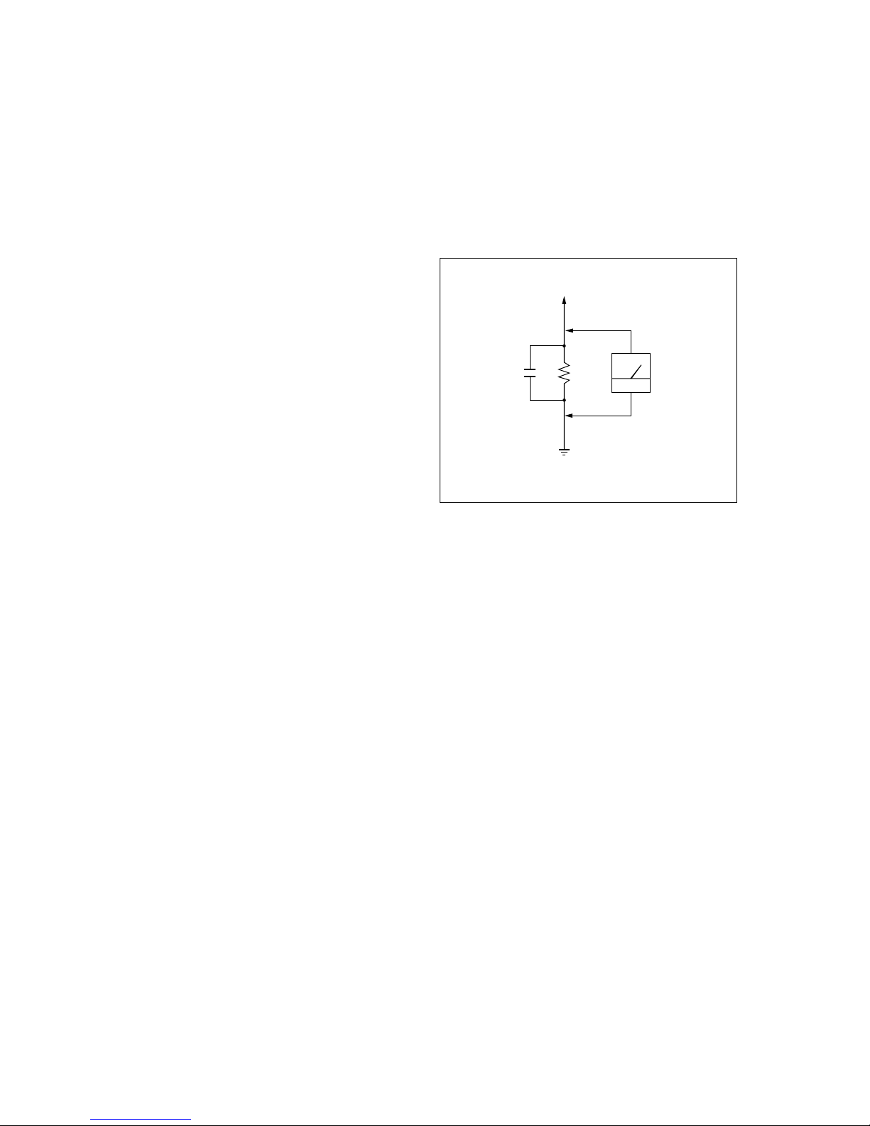
To Exposed Metal
Parts on Set
AC
0.15
1.5k
µ
F
Ω
Voltmeter
(0.75V)
Earth Ground
Fig. A. Using an AC voltmeter to check AC leakage.
– 4 –
SECTION 1
SERVICING NOTES
NOTES ON HANDLING THE OPTICAL PICK-UP BLOCK
OR BASE UNIT
The laser diode in the optical pick-up block may suffer electrostatic
breakdown because of the potential difference generated by the
charged electrostatic load, etc. on clothing and the human body.
During repair, pay attention to electrostatic breakdown and also use
the procedure in the printed matter which is included in the repair
parts.
The flexible board is easily damaged and should be handled with
care.
NOTES ON LASER DIODE EMISSION CHECK
The laser beam on this model is concentrated so as to be focused on
the disc reflective surface by the objectiv e lens in the optical pick-up
block. Therefore, when checking the laser diode emission, observe
more than 30 cm away from the objective lens.
r Tray (Slide) getting out procedure on the power supply is OFF
Rotate the BU CAM assembly in the direction of the arrow and pull out the slide.
CHUCK PLATE JIG ON REPAIRING
On repairing CD section, playing a disc without the CD lid, use Chuck
Plate Jig.
r Code number of Chuck Plate Jig : X-4918-255-1
Tray (Slied)
21
BU CAM assy
– 5 –
SECTION 2
GENERAL
This section is extracted from
instruction manual.
(HCD-H331)
– 6 –
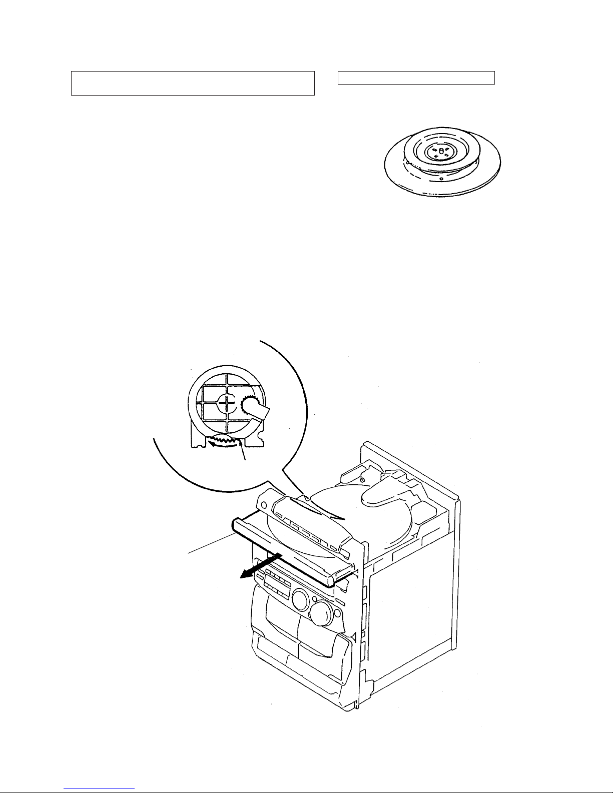
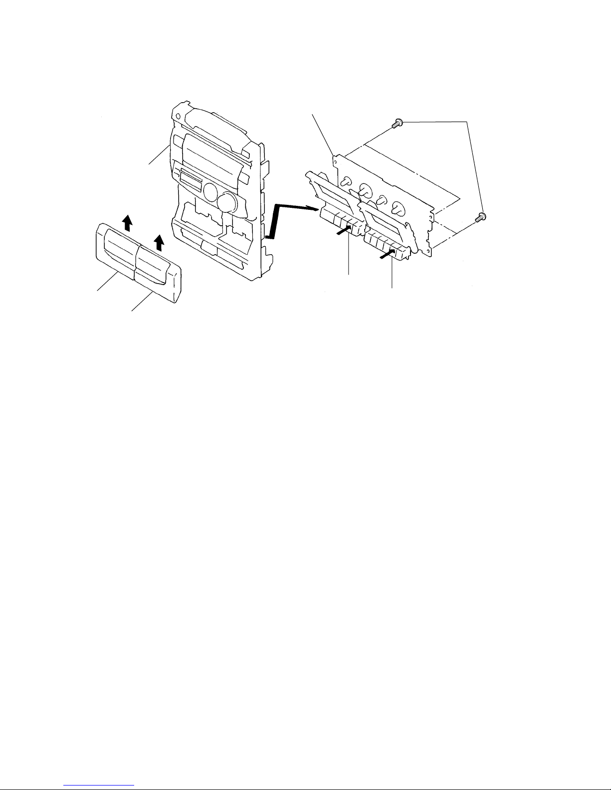
DISASSEMBLY
Note : Follow the disassembly procedure in the numerical order given.
3-1. FRONT PANEL REMOVAL
SECTION 3
3-2. CD BLOCK REMOVAL
1
Screw
+BVTT 3X8 (S)
2
Loading panel
CD block (CDM38-5BD19)
3
1
Screw
+BVTT 3X8 (S)
– 7 –
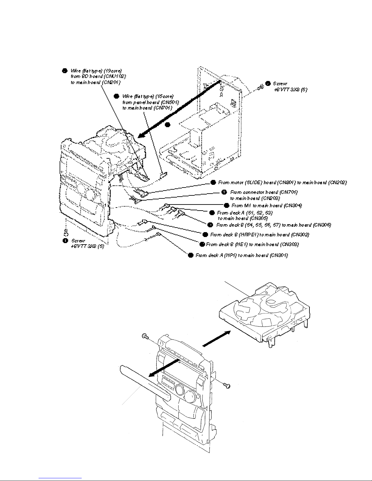
3-3. LID (A)/(B) ASSY, CASSETTE, MECHANISM DECK BLOCK REMOVAL
Front panel section
Lid (A) assy, Cassette
Lid (B) assy, Cassette
2
2
Mechanism deck block (TCM-YSW47C24)
4
1
1
Button (EJECT)
Button (EJECT)
3
Screw
+BVTP 2.6X8
– 8 –
SECTION 4
AF OSC
attenuator
47k
Ω
47k
Ω
51.2mV (–23.6dB)
CN307
R-CH
L-CH
CN308
MAIN BOARD
(Component side)
– Input point –
Output level
– measurement –
point
3
3
1
1
Output level
measurement
point
SECTION 5
MECHANICAL ADJUSTMENTS
PRECAUTION
1. Clean the following parts with a denatured-alcohol-moistened
swab :
record/playback head pinch rollers
erase head rubber belts
capstan
2. Demagnetize the record/playback head with a head demagnetizer.
3. Do not use a magnetized screwdriver for the adjustments.
4. After the adjustments, apply suitable locking compound to the
parts adjusted.
5. The adjustments should be performed with the rated power supply voltage unless otherwise noted.
rTorque Measurement
Mode Torque meter Meter reading
FWD CQ-102C
FWD
Back Tension
CQ-102C
FF/REW CQ-201B
30 to 80 g • cm
(0.42–1.11 oz• inch)
1.5 to 5.5 g • cm
(0.021–0.076 oz• inch)
55 to 130 g • cm
(0.77–1.80 oz• inch)
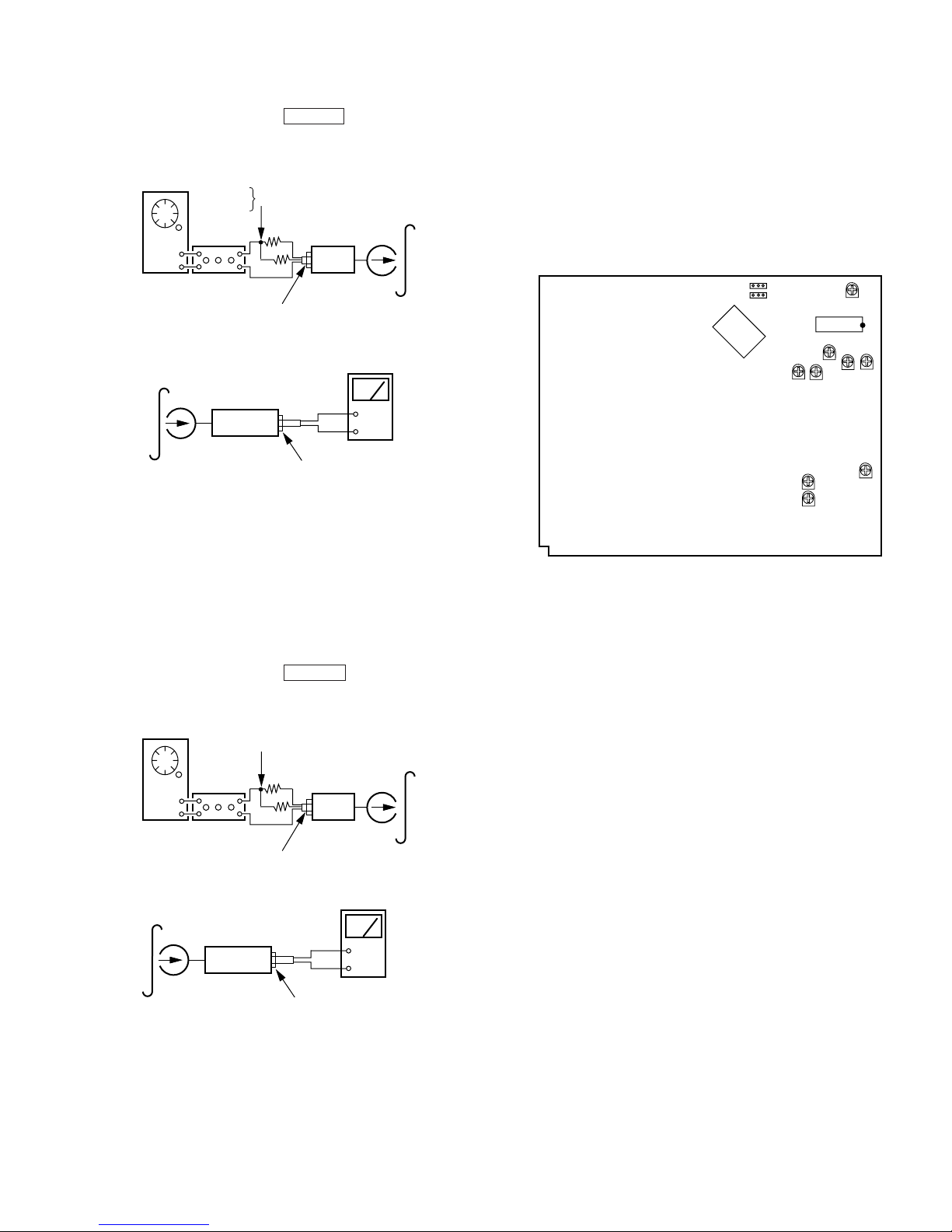
ELECTRICAL ADJUSTMENTS
DECK SECTION
1. The adjustment should be performed in the publication.
(Be sure to make playback adjustment at first.)
2. The adjustment and measurement should be performed for both
L-CH and R-CH.
r Switch position
DOLBY NR switch : OFF
FUNCTION button : OFF
EFECT switch : OFF
DBFB switch : OFF
3. Input point and output level measurement point.
rTape T ension Measurement
Torque Meter Meter Reading
CQ-403A
more than 100g
(more than 3.53 oz)
r
Tast tape
Tape Contents Use
P-4-A100 10kHz, –10dB Head Azimuth Adjustment
P-4-L300 315Hz, 0dB Level Adjustment
WS-48B 3kHz, 0dB Tape Speed Adjustment
0db=0.775V
Record/Playback Head Azimuth Adjustment
DECK A DECK B
Procedure :
1. Mode : Playback
test tape
P-4-A100
(10kHz, – 10dB)
set
Output level measurement point
level meter
+
–
– 9 –
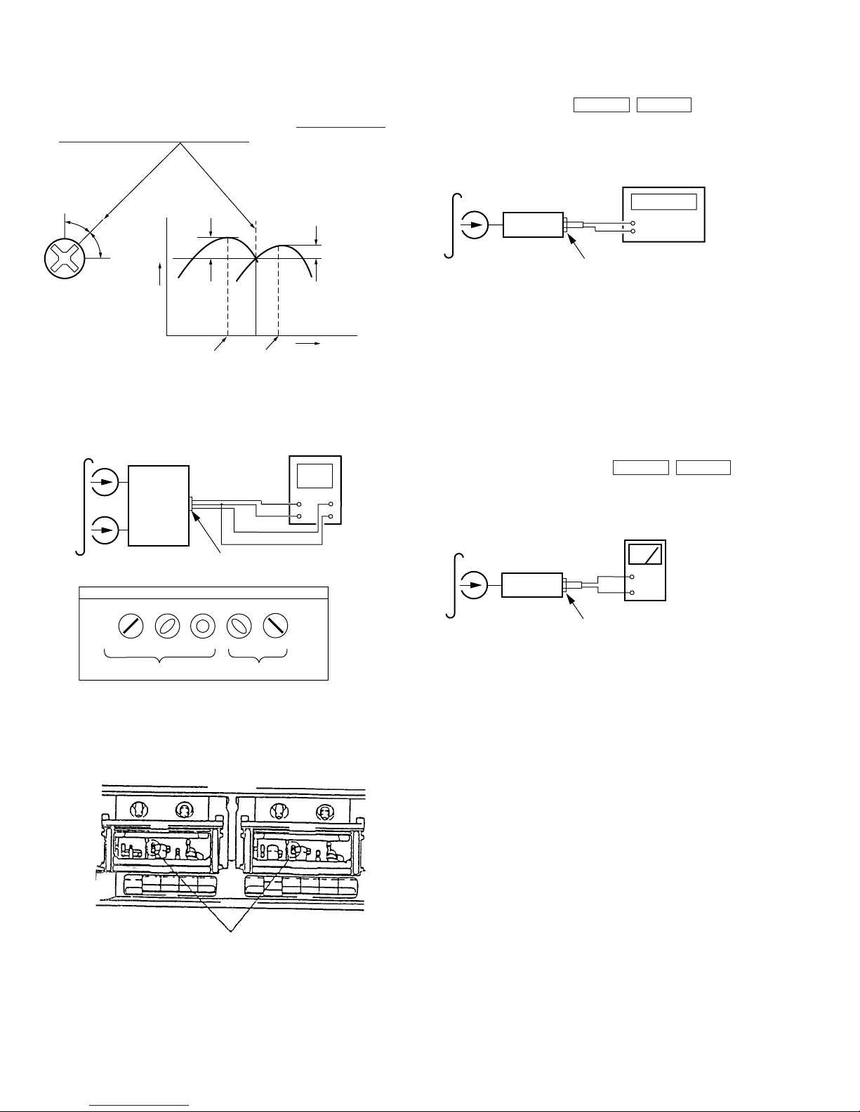
r
2. Turn the adjustment scre w for the maximum output levels. If these
levels do not match, turn the adjustment screw until both of output levels match together within 1dB.
L-CH
peak
within
Screw
position
R-CH
peak
output
level
1 dB
L-CH
peak
R-CH
peak
within
1 dB
screw position
3. Mode : Playback
test tape
P-4-A100
(10kHz, –10dB)
L-CH
set
R-CH
L
R
Output level measurement point
(see page 9)
screen pattern
oscilloscope
V
H
Tape Speed Adjustment DECK A DECK B
Procedure :
Mode : Playback
test tape
WS-48B
(3kHz, – 0dB)
set
Output level measurement point
(see page 9)
frequency counte
+
–
1. Set to FWD playback mode.
2. Adjust RV380 so that the frequency counter r eading becomes 3,000
± 15Hz.
r Frequency difference between the begining and the end of the tape
should be within ± 3%.
r Frequency difference between deck A and deck B the bigining of
the tape should be within 1.5%.
Adjustment Location : MAIN board. (see page 11)
Playback Level Adjustment DECK A DECK B
Procedure :
Mode : Playback
test tape
P-4-L300
(315Hz, 0dB)
set
level meter
+
–
in phase 45° 90° 135° 180
good
°
wrong
4. Change the review playback mode and repeat the steps 1 to 3.
5. After the adjustment, lock the adjustment screw with suitable locking compound.
Adjustment Location :
Adjustment screws
REC/PB head (deck B)
or PB head (deck A)
Output level measurement point
(see page 9)
Deck A is RV301 (L-CH) and RV401 (R-CH), deck B is RV302 (LCH) and RV402 (R-CH) so that adjustment within adjustment level
as follows.
Adjustment Level :
OUTPUT level : –7.2 to –8.2dB (– 301.5 to 338.3 mV)
level Difference between Channels : within 0.5dB
Comfrim the OUTPUT level does not change in playback mode while
changing the mode from playback to stop several times.
Adjustment Location : MAIN board. (see page 11)
– 10 –
CN307
RV304
RV404
RV380
RV401
RV301
RV402
RV403
RV302
RV303
IC303
IC901
CN308
Record Bias Adjustment DECK B
Procedure :
1. Mode : record
AF OSC
1) 315 Hz
2) 10kHz
attenuator
51.2mV (–23.6dB)
47k
Ω
47k
Input point (see page 9)
set
Ω
2. Mode : Playback
record
portion
blank tape
CS-123
level meter
Adjustment Level :
OUTPUT level : –23.3dB to –24.3dB (47.3 to 53.1mV)
Adjustment Location : MAIN board.
Adjustment Location :
[ MAIN BOARD ] – Component side –
set
+
–
Output level measurement point
(see page 9)
3. Confirm playback the signal recorded in step1 become adjustment
level as follows.
4. If these levels do not adjustment lev el, adjustment the RV304 (LCH) and RV404 (R-CH) to repeat step 1 and 4.
Adjustment level : Playback output of 315Hz to playback output
of 10kHz : 0 ± 0.5dB
Adjustment Location : MAIN board.
Record Level Adjustment DECK B
Procedure :
1. Mode : record
AF OSC
315Hz 51.2mV (–23.6dB)
47k
attenuator
Ω
47k
Ω
Input point (see page 9)
set
blank tape
CS-123
2. Mode : playback
record
portion
level meter
set
3. Confirm playback the signal recorded in step1 become adjustment
level as follows.
Output level measurement point
(see page 9)
4. If these levels do not adjustment lev el, adjustment the RV303 (LCH) and RV403 (R-CH) to repeat steps 1 and 2.
+
–
– 11 –

CD SECTION
s
+
–
oscilloscope
TP (RF)
BD board
TP (VC)
Note :
1. CD Block basically constructed to operate without adjustment.
Therefore, check each item in order given.
2. Use YEDS-18 disc (3-702-101-01) unless otherwise indicated.
3. Use the oscilloscope with more than 10MΩ impedance.
4. Clean an object lens by an applicator with neutral detergent when
the signal level is low than specified value with the following
checks.
Focus Bias Adjustment
This adjustment is to be done when the optical block is replaced.
5. Check the oscilloscope waveform (S-curve) is symmetrical
between A and B. And confirm peak to peak level within
2.4 ± 0.7Vp-p.
S-curve waveform
symmetry
A
within 2.4
B
±
0.7Vp-p
Adjustment procedure :
oscilloscope
(DC range)
BD board
TP (RF)
TP (VC)
+
–
1. Connect oscilloscope to test point TP (VC) and TP (RF) on BD
board.
2. Turned power switch ON. (Stop mode)
3. Put disc (YEDS-18) in and press the fl button.
4. Adjust RV101 so that the oscilloscope waveform is as shown in
the figure below (eye pattern).
A good eye pattern means that the diamond shape (◊) in the center
of the waveform can be clearly distinguished.
r
RF signal reference waveform (eye pattern)
VOLT/DIV : 0.2V
TIME/DIV : 500n
1.3 ± 0.3Vp-p
6. After check, remove the lead wire connected in step 2.
Note : r Try to measure several times to make sure that the ratio of
A : B or B : A is more than 10 : 7.
r Take sweep time as long as possible and light up the bright-
ness to obtain best waveform.
Adjustment Location : BD board. (see page 13)
RF Level Check
Procedure :
1. Connect oscilloscope to test point TP (VC) and TP (RF) on BD
board.
2. Turned Power switch on.
3. Put disc (YEDS-18) in and press the fl button.
4. Confirm that oscilloscope wav eform is clear and check RF signal
level is correct or not.
Note :
Clear RF signal waveform means that the shape “◊” can be clearly
distinguished at the center of the waveform.
r
RF signal waveform
When observing the eye pattern, set the oscilloscope for A C range
and raise vertical sensitivity.
Adjustment Location : MAIN board. (see page 13)
S-Curve Check
oscilloscope
BD board
TP (FEO)
TP (VC)
+
–
Procedure :
1. Connect oscilloscope to test point TP (VC) and TP (FEO) on BD
board.
2. Connect between test point TP (FOK) and GND by lead wire.
3. Turned Power switch on.
4. Put disc (YEDS-18) in and turned Power switch on again and
actuate the focus search. (actuate the focus search when disc table
is moving in and out.)
VOLT/DIV : 200mV
TIME/DIV : 500ns
level : 1.3
±
0.3Vp-p
Adjustment Location : BD board. (see page 13)
– 12 –

E-F Balance Check
oscilloscope
(DC range)
BD board
TP (TEO)
TP (VC)
+
–
Procedure :
1. Ground main board IC701 (pin #ª) with the lead wire.
2. Connect oscilloscope to test point TP (VC) and TP (TEO) on BD
board.
3. Turned Power switch on.
4. Put disc (YEDS-18) in and press the fl button.
5. Confirm that the osilloscope waveform is symmetrical on the
top and bottom in relation to 0V, and check this level.
Traverse waveform
A
0V
B
level : 300 ± 100mVp-p
specified value : r
A–B
2 (A+B)
r
A+B = 300 ± 100mVp-p
X100 = less than ± 7%
6. Remove the lead wire connected in step 1.
Focus/Tracking Gain Adjustment (RV102, RV103)
This gain has a margin, so even if it is slightly off. There is no problem.
Therefore, do not perform, this adjustment.
Please note that it should be fixed to mechanical center position when
you moved and do not know original position.
Adjustment Location :
[BD BOARD] (Conductor side)
FOK
IC102
FEI
TEI
PCK
FEO
TEO
RV103
RV102
VC
RF
IC101
RV101
GND
IC104
– 13 –

SECTION 6
EXPLANATION OF IC TERMINALS
IC501 ASD042 (SYSTEM CONTROL /FL DRIVE)
Pin No. Pin name I/O Description
1-7 GR1-7 O FL grid signal output.
8VDD – +5V
9, 10 LED9, 10 O LED drive signal open.
11 KEY SELECT O Not used. (Open)
12 VOL IN B I Volume encoder signal input.
13 REQ. GM I/O Request signal from/ to master control.
14 CLK MG I Serial clock input.
15 DATA GM O Serial data output.
16 DATA MG I Serial data input.
17 RESET I Reset signal input.
18 PANEL SW I CD door open detection input. Not used. (Open)
19 LED SELECT O LED select signal output.
20 AVSS – Ground.
21-24 SPEANA IN1-4 I Spectram analizer signal input. Not used (Ground)
25-28 KEY IN 1-4 I Key matrix input.
29 AVDD –
30 AVREF –
31 JOG IN B I Not used. (Ground)
32 XT2 I Not used. (Open)
33 VSS – Ground.
34 X1 I
35 X2 O
36, 37 LED7, 8 O LED drive signal output.
38, 39 LED5, 6 O Not used. (Open)
40-43 LED1-4 O LED drive signal output.
44 VOL IN A I Volume encoder signal input.
45 JOG IN A I Not used. (Ground)
46 RDY MG I RDY signal from master control.
47 SIRCS IN I SIRCS signal input.
48 IC (VPP) – Ground connection.
49-51 LEDS11-13 O LED drive signal output.
52 VDD – Not used.
53-70 SEG5-22 O FL segment signal output.
71 V. LOAD – –25V for FL
72-75 SEG1-4 O FL segment signal output.
76-80 GR8-12 O FL grid signal output
r Abbreviation
FL : FLUORESCENT INDICATOR TUBE
+5V.
X’tal (5MHz)
– 14 –
 Loading...