

Page 1
HCD-GZR7D/GZR8D/
GZR9D
SERVICE MANUAL
Ver. 1.0 2008.05
• HCD-GZR7D/GZR8D/GZR9D are the
tuner, deck, DVD and amplifi er section
in MHC-GZR7D/GZR8D/GZR9D.
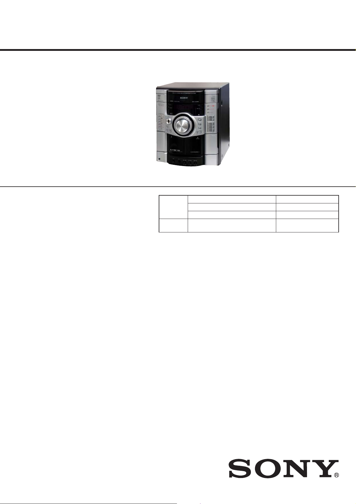
Photo: HCD-GZR8D
DVD
Section
Tape Deck
Section
E Model
HCD-GZR7D/GZR8D/GZR9D
Australian Model
HCD-GZR9D
Model Name Using Similar Mechanism HCD-GNZ777D/GNZ888D
DVD Mechanism Type CDM74HF-DVBU101//C
Optical Pick-up Name KHM-313CAB/C2RP
Model Name Using Similar Machanism HCD-GNZ777D/GNZ888D
Amplifi er Section
The following measured at AC 120, 220, 240 V, 50/60 Hz
MHC-GZR9D
Power output (rated): 100 W + 100 W (6 Ω at 1 kHz, 1% THD)
RMS output power (reference)
Front speaker: 180 W + 180 W (per channel at 6 Ω, 1 kHz,
10% THD)
Center speaker: 60 W (6 Ω at 1 kHz, 10% THD)
Surround speaker: 60 W + 60 W (per channel at 6 Ω, 1 kHz,
10% THD)
Subwoofer: 180 W (6 Ω at 80 Hz, 10% THD)
MHC-GZR8D
Power output (rated): 100 W + 100 W (6 Ω at 1 kHz, 1% THD)
RMS output power (reference)
Front speaker: 180 W + 180 W (per channel at 6 Ω, 1 kHz,
10% THD)
Center speaker: 60 W (6 Ω at 1 kHz, 10% THD)
Surround speaker: 60 W + 60 W (per channel at 6 Ω, 1 kHz,
10% THD)
SPECIFICATIONS
MHC-GZR7D
Power output (rated): 100 W + 100 W (6 Ω at 1 kHz, 1% THD)
RMS output power (reference):
180 W+ 180 W (per channel at 6 Ω, 1 kHz,
10% THD)
Inputs
VIDEO/SAT VIDEO IN (phono jack):
1 Vp-p, 75 ohms
VIDEO/SAT AUDIO IN L/R (phono jacks):
voltage 250/450 mV, impedance 47 kilohms
MIC 1/MIC 2 (phone jacks):
sensitivity 1 mV, impedance 10 kilohms
– Continued on next page –
9-889-156-01
2008E04-1
2008.05
©
DVD DECK RECEIVER
Sony Corporation
Audio Business Group
Published by Sony Techno Create Corporation
Page 2

HCD-GZR7D/GZR8D/GZR9D
Outputs
VIDEO OUT (phono jack):
max. output level 1 Vp-p, unbalanced, Sync
negative, load impedance 75 ohms
S VIDEO OUT (4-pin/mini-DIN jack):
Y: 1 Vp-p, unbalanced, Sync negative,
C: 0.286 Vp-p, load impedance 75 ohms
COMPONENT VIDEO OUT:
Y: 1 Vp-p, 75 ohms
PB/CB: 0.7 Vp-p, 75 ohms
P
DVD DIGITAL OUT (MHC-GZR7D only)
(Square optical connector jack, rear panel):
Wavelength 660 nm
PHONES (stereo mini jack):
accepts headphones of 8 ohms or more
SUBWOOFER OUT (MHC-GZR8D/GZR7D only):
Voltage 1 V, impedance 1 kilohms
FRONT SPEAKER:
MHC-GZR9D: Use only the supplied speaker SS-GZR9D.
MHC-GZR8D/GZR7D:
Use only the supplied speaker SS-GZR8D.
SURROUND SPEAKER (MHC-GZR9D/GZR8D only):
Use only the supplied speaker SS-RSX9D.
CENTER SPEAKER (MHC-GZR9D/GZR8D only):
Use only the supplied speaker SS-CTX9D.
SUBWOOFER (MHC-GZR9D only):
Use only the supplied subwoofer SS-WGV9D.
R/CR: 0.7 Vp-p, 75 ohms
USB section
Supported bit rate MP3 (MPEG 1 Audio Layer-3): 32 – 320 kbps
WMA: 48 – 192 kbps
AAC: 48 – 320 kbps
Sampling frequencies
MP3 (MPEG 1 Audio Layer-3): 32/44.1/48 kHz
WMA: 44.1 kHz
AAC: 44.1 kHz
(USB) port: Maximum current: 500 mA
Disc player section
System: Compact disc and digital audio and video system
Laser Diode Properties
Emission duration: Continuous Laser Output*:
Less than 44.6μW
*This output is the value measurement at a distance
of 200mm from the objective lens surface on the
Optical Pick-up Block with 7mm aperture.
Frequency response DVD (PCM 48 kHz): 2 Hz – 22 kHz (±1 dB)
CD: 2 Hz – 20 kHz (±0.5 dB)
Video color system format
NTSC and PAL
Tape deck section
Recording system: 4-track 2-channel, stereo
Tuner section
FM stereo, FM/AM superheterodyne tuner
FM tuner section
Tuning range: 87.5 – 108.0 MHz (50 kHz step)
Antenna: FM lead antenna
Antenna terminals: 75 Ω unbalanced
Intermediate frequency:
10.7 MHz
AM tuner section
Tuning range:
Australian model: 531 – 1,710 kHz (with 9 kHz tuning interval)
530 – 1,710 kHz (with 10 kHz tuning interval)
Other models: 531 – 1,602 kHz (with 9 kHz tuning interval)
530 – 1,610 kHz (with 10 kHz tuning interval)
Antenna: AM loop antenna
Antenna terminals: External antenna terminal
Intermediate frequency:
450 kHz
General
Power requirements
Australian model: AC 230 – 240 V, 50/60 Hz
Thai model: AC 220 V, 50/60 Hz
Other models: AC 120, 220, 230 – 240 V, 50/60 Hz, adjustable
with voltage selector
Power consumption
MHC-GZR9D: 270 W
MHC-GZR8D: 240 W
MHC-GZR7D: 170 W
Dimensions (w/h/d) (excl. speakers)
MHC-GZR9D: Approx. 280 × 325 × 415 mm
MHC-GZR8D/GZR7D:
Approx. 280 × 325 × 382 mm
Mass (excl. speakers)
MHC-GZR9D: Approx. 12 kg
MHC-GZR8D: Approx. 11.5 kg
MHC-GZR7D: Approx. 10.5 kg
Design and specifi cations are subject to change without notice.
SAFETY-RELATED COMPONET WARNING!
COMPONENTS IDENTIFIED BY MARK 0 OR DOTTED LINE
WITH MARK 0 ON THE SCHEMATIC DIAGRAMS AND IN
THE PARTS LIST ARE CRITICAL TO SAFE OPERATION.
REPLACE THESE COMPONENTS WITH SONY PARTS
WHOSE PART NUMBERS APPEAR AS SHOWN IN THIS
MANUAL OR IN SUPPLEMENTS PUBLISHED BY SONY.
2
Page 3

HCD-GZR7D/GZR8D/GZR9D
NOTES ON CHIP COMPONENT REPLACEMENT
• Never reuse a disconnected chip component.
• Notice that the minus side of a tantalum capacitor may be damaged by heat.
FLEXIBLE CIRCUIT BOARD REPAIRING
• Keep the temperature of soldering iron around 270 °C during
repairing.
• Do not touch the soldering iron on the same conductor of the
circuit board (within 3 times).
• Be careful not to apply force on the conductor when soldering
or unsoldering.
UNLEADED SOLDER
Boards requiring use of unleaded solder are printed with the leadfree mark (LF) indicating the solder contains no lead.
(Caution: Some printed circuit boards may not come printed with
the lead free mark due to their particular size)
: LEAD FREE MARK
Unleaded solder has the following characteristics.
• Unleaded solder melts at a temperature about 40 °C higher
than ordinary solder.
Ordinary soldering irons can be used but the iron tip has to be
applied to the solder joint for a slightly longer time.
Soldering irons using a temperature regulator should be set to
about 350 °C.
Caution: The printed pattern (copper foil) may peel away if
the heated tip is applied for too long, so be careful!
• Strong viscosity
Unleaded solder is more viscous (sticky, less prone to fl ow)
than ordinary solder so use caution not to let solder bridges
occur such as on IC pins, etc.
• Usable with ordinary solder
It is best to use only unleaded solder but unleaded solder may
also be added to ordinary solder.
NOTES ON LASER DIODE EMISSION CHECK
The laser beam on this model is concentrated so as to be focused
on the disc refl ective surface by the objective lens in the optical
pickup block. Therefore, when checking the laser diode emission,
observe from more than 30 cm away from the objective lens.
Laser component in this product is capable of emitting radiation
exceeding the limit for Class 1.
This appliance is classifi ed as
a CLASS 1 LASER product.
This marking is located on the
rear exterior.
CAUTION
Use of controls or adjustments or performance of procedures
other than those specifi ed herein may result in hazardous radia-
tion exposure.
NOTES ON HANDLING THE OPTICAL PICK-UP
BLOCK OR BASE UNIT
The laser diode in the optical pick-up block may suffer electrostatic break-down because of the potential difference generated by the
charged electrostatic load, etc. on clothing and the human body.
During repair, pay attention to electrostatic break-down and also
use the procedure in the printed matter which is included in the
repair parts.
The fl exible board is easily damaged and should be handled with
care.
3
Page 4
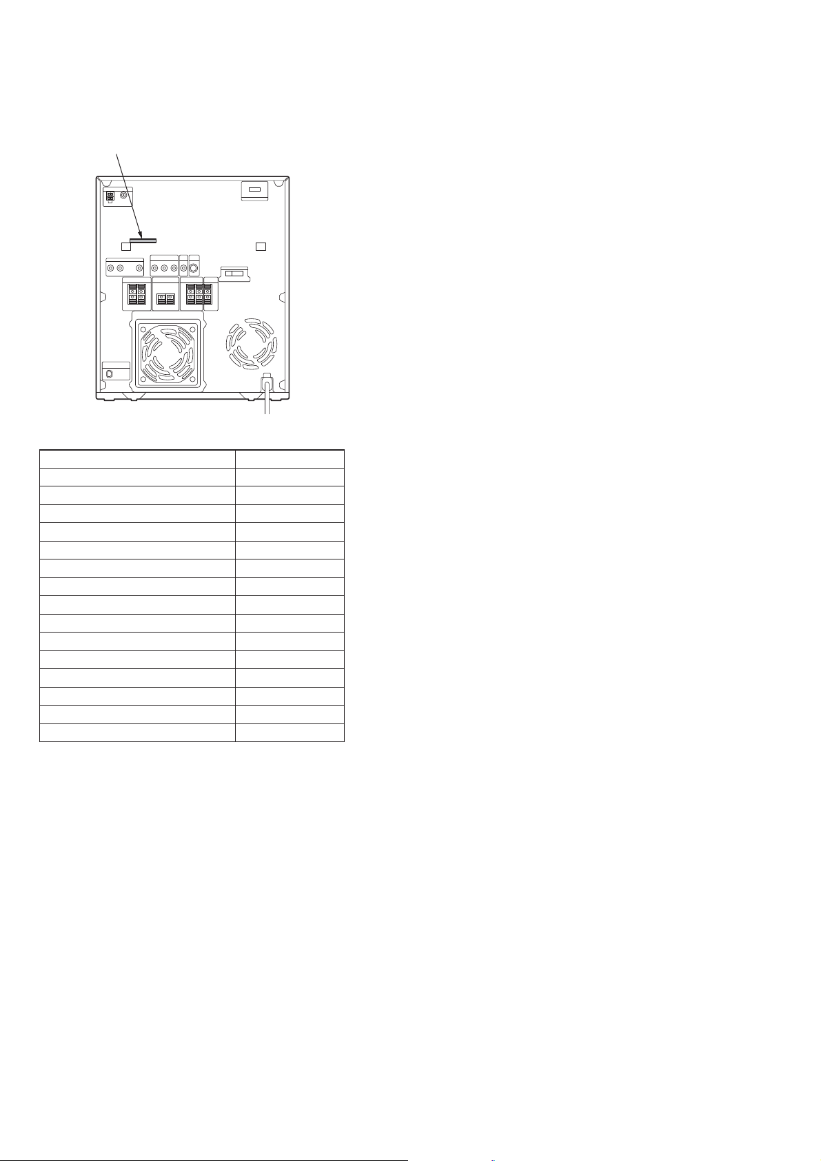
HCD-GZR7D/GZR8D/GZR9D
MODEL IDENTIFICATION
– Back Panel –
Parts No.
Model Parts No.
GZR9D: E3, E15
GZR9D: SP
GZR9D: PH
GZR9D: E2
GZR9D: AUS
GZR8D: E3, E15
GZR8D: E12
GZR8D: SP
GZR8D: TH
GZR8D: PH
GZR7D: E3, E15
GZR7D: E12
GZR7D: SP
GZR7D: TH
GZR7D: PH
• Abbreviation
E2 : 120V AC area in E model
E3 : 240V AC area in E model
E12 : 220 – 240V AC area in E model
E15 : Iran model
PH : Philippines model
SP : Singapore model
TH : Thai model
AUS : Australian model
3-285-875-1[]
3-285-875-4[]
3-285-875-6[]
3-285-875-7[]
3-285-875-8[]
3-291-798-1[]
3-291-798-3[]
3-291-798-4[]
3-291-798-5[]
3-291-798-6[]
3-291-799-1[]
3-291-799-3[]
3-291-799-4[]
3-291-799-5[]
3-291-799-6[]
4
Page 5

TABLE OF CONTENTS
HCD-GZR7D/GZR8D/GZR9D
1. SERVICING NOTES ............................................. 6
2. GENERAL
Guide to parts and controls ............................................. 8
3. DISASSEMBLY
3-1. Case ................................................................................. 20
3-2. Loading Panel ................................................................. 20
3-3. Tuner Pack, DMPORT Board ......................................... 21
3-4. DVD Block Section ........................................................ 21
3-5. Front Panel Section ......................................................... 22
3-6. SUB-TRANS Board ....................................................... 22
3-7. Back Panel Section ......................................................... 23
3-8. Boards Section ................................................................ 23
3-9. SURR & CENT AMP Board
(HCD-GZR8D/GZR9D) ................................................. 24
3-10. MAIN Board ................................................................... 24
3-11. REGULATOR Board ...................................................... 25
3-12. AMP FR & SW Board .................................................... 25
3-13. Tape Mechanism Deck .................................................... 26
3-14. MIC Board, HEADPHONE Board ................................. 26
3-15. Lid (TC-L), Lid (TC-R) .................................................. 27
3-16. PANEL Board, VOLUME Board,
KEY-RIGHT Board ........................................................ 27
3-17. USB Board ...................................................................... 28
3-18. KEY-LEFT Board ........................................................... 28
3-19. VIDEO Board ................................................................. 29
3-20. DMB18 Board ................................................................. 29
3-21. DVD Assy ....................................................................... 30
3-22. Optical Pick-up ............................................................... 30
3-23. DRIVER Board, SW Board ............................................ 31
3-24. SENSOR Board .............................................................. 31
3-25. MOTOR (TB) Board....................................................... 32
3-26. MOTOR (LD) Board ...................................................... 32
7-6. Printed Wiring Boards –Driver Section– ........................ 49
7-7. Schematic Diagram –Driver Section– ............................ 50
7-8. Printed Wiring Board –DMB18 Board (1/2)– ................ 51
7-9. Printed Wiring Board –DMB18 Board (2/2)– ................ 52
7-10. Schematic Diagram –DMB18 Board (1/5)– ................... 53
7-11. Schematic Diagram –DMB18 Board (2/5)– ................... 54
7-12. Schematic Diagram –DMB18 Board (3/5)– ................... 55
7-13. Schematic Diagram –DMB18 Board (4/5)– ................... 56
7-14. Schematic Diagram –DMB18 Board (5/5)– ................... 57
7-15. Printed Wiring Board –Main Section– ............................ 58
7-16. Schematic Diagram –Main Section (1/4)– ...................... 59
7-17. Schematic Diagram –Main Section (2/4)– ...................... 60
7-18. Schematic Diagram –Main Section (3/4)– ...................... 61
7-19. Schematic Diagram –Main Section (4/4)– ...................... 62
7-20. Printed Wiring Boards –Mic/Headphone Section– ......... 63
7-21. Schematic Diagram –Mic/Headphone Section– ............. 64
7-22. Printed Wiring Board –TC Section– ............................... 65
7-23. Schematic Diagram –TC Section– .................................. 66
7-24. Printed Wiring Board –Video Section–........................... 67
7-25. Schematic Diagram –Video Section– ............................. 68
7-26. Printed Wiring Board –DMPORT Section– .................... 69
7-27. Schematic Diagram –DMPORT Section– ...................... 70
7-28. Printed Wiring Boards –Regulator/USB Section– .......... 71
7-29. Schematic Diagram –Regulator/USB Section– .............. 72
7-30. Printed Wiring Boards –Panel Section– .......................... 73
7-31. Schematic Diagram –Panel Section– .............................. 74
7-32. Printed Wiring Boards –Front Speaker Section– ............ 75
7-33. Schematic Diagram –Front Speaker Section– ................ 76
7-34. Printed Wiring Boards –Surround/Center Speaker,
Subwoofer Section– (HCD-GZR8D/GZR9D) ................ 77
7-35. Schematic Diagram –Surround/Center Speaker,
Subwoofer Section– (HCD-GZR8D/GZR9D) ................ 78
7-36. Printed Wiring Boards –Power Section– ........................ 79
7-37. Schematic Diagram –Power Section– ............................. 80
4. TEST MODE ............................................................ 33
5. MECHANICAL ADJUSTMENTS ...................... 38
6. ELECTRICAL ADJUSTMENTS ........................ 39
7. DIAGRAMS
7-1. Block Diagram –RF/Servo Section– ............................... 43
7-2. Block Diagram –Video Section– .................................... 44
7-3. Block Diagram –Main Section– ..................................... 45
7-4. Block Diagram –Audio Section– .................................... 46
7-5. Block Diagram –Display/Power Section– ...................... 47
8. EXPLODED VIEWS
8-1. Overall Section ............................................................... 93
8-2. Front Panel Section-1 ...................................................... 94
8-3. Front Panel Section-2 ...................................................... 95
8-4. Back Panel Section ......................................................... 96
8-5. Chassis Section ............................................................... 97
8-6. DVD Block Section ........................................................ 98
8-7. DVD Mechanism Deck Section-1 .................................. 99
8-8. DVD Mechanism Deck Section-2 .................................. 100
9. ELECTRICAL PARTS LIST .............................. 101
5
Page 6
HCD-GZR7D/GZR8D/GZR9D
SECTION 1
SERVICING NOTES
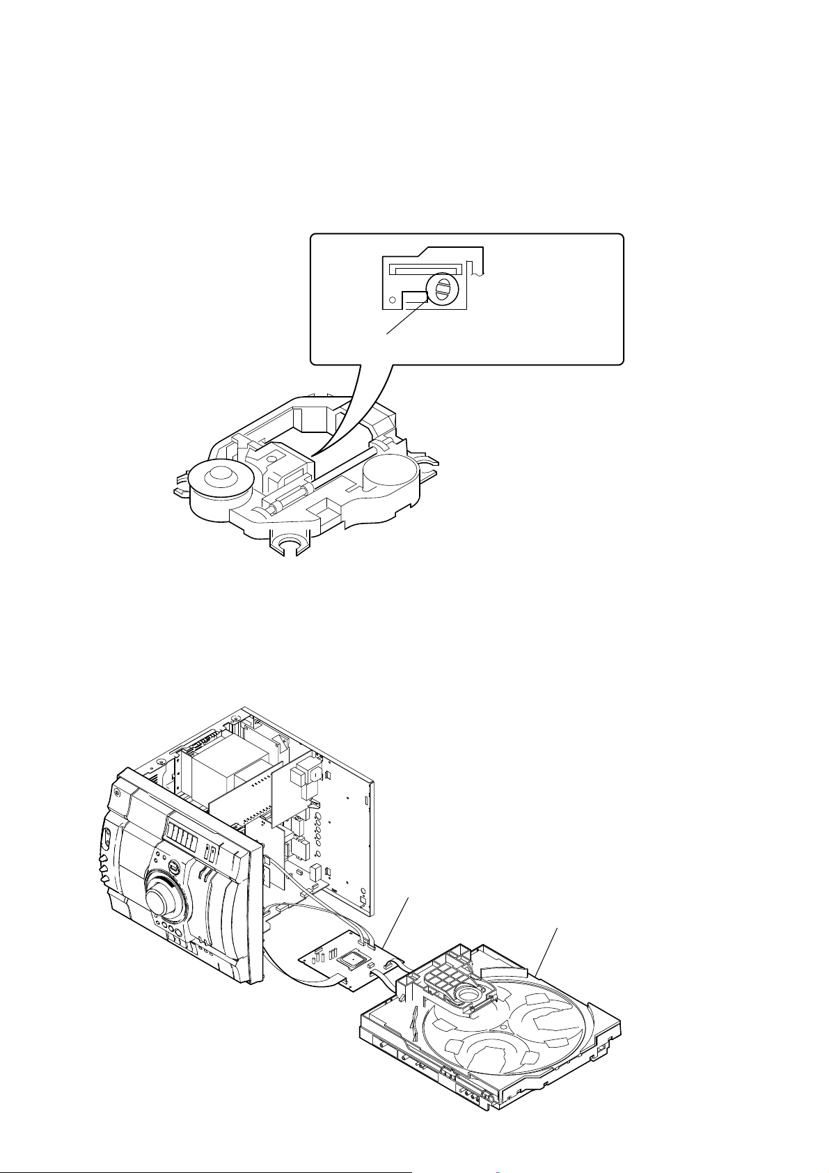
Notes on Disconnecting Between the OP Section (DVBU101) and the DMB18 Board
Note: When disconnecting between the OP section (DVBU101) and the DMB18 board, be sure to make a solder brige for electrostatic
prevention as illustrated in the fi gure (before disconnection).
On the contrary, when installing the OP section, never remove the solder bride until the OP section and the DMB18 board are
connected.
Be sure to remove the solder bridge after the OP section and the DMB18 board have been connected.
Perform solder bridging to prevent damage by electrostatic
discharge when handling the BU as a single unit.
Service Position for the DVD Mechanism Deck Section
Refer to the fi gure given below when disassembling the DVD mechanism deck section.
DMB18 board
DVD mechanism deck section
6
Page 7
HCD-GZR7D/GZR8D/GZR9D
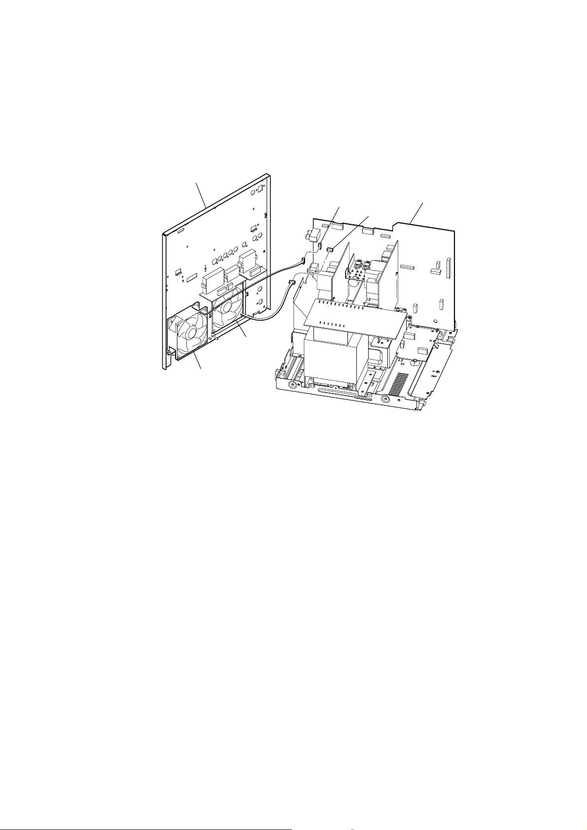
Notes on Installing the Two Cooling Fans (FAN901 and FAN902) (HCD-GZR8D/GZR9D)
Note: The HCD-GZR8D/GZR9D has two cooling fans (FAN901 and FAN902) used. The connectors of these fans have the same color
and the same number of pins.
When installing these fans, check the marking of CN601 and CN602 on the MAIN board and ensure that they are located correctly.
The CN601 on the MAIN board is to be attached with the connector of FAN901 where as the CN602 is to be attached with the
connector of FAN902.
back panel
FAN901
FAN902
CN601
MAIN board
CN602
7
Page 8
HCD-GZR7D/GZR8D/GZR9D
Guide to parts and controls
also be performed using the buttons on the unit having the same or similar names.
Unit
SECTION 2
GENERAL
This section is extracted
from instruction manual.
GB
12
8
Page 9
HCD-GZR7D/GZR8D/GZR9D
Remote
@/ (on/standby) (24, 79, 106,
129)
Unit: STANDBY indicator (118)
Remote: TV @/
1)
(on/standby)
(29)
DISPLAY (27, 33, 73, 107, 108)
Press to display the disc information or
clock in the front panel display.
Unit: ILLUMINATION (108, 129)
Press to change the illumination pattern
around MASTER VOLUME0.
Display
Disc tray
Remote sensor
Guide to parts and controls
Continued
M
13
GB
9
Page 10

HCD-GZR7D/GZR8D/GZR9D
ENTER (28, 33, 34, 39, 44, 49, 53,
58, 59, 60, 63, 71, 74, 76, 79, 83,
87, 95, 102, 105, 129)
Press to enter the settings.
SOUND FIELD (95)
surround sound.
Unit: GROOVE (94)
Press to reinforce the bass.
Unit: PRESET EQ (94)
Unit: EQ BAND/MEMORY (95)
Press to select the frequency band when
adjusting the equalizer.
REC TO USB (79, 83)
Press to transfer music from a disc or
record the sound from an analog audio
source to the connected optional USB
device.
Press to mark track numbers during
recording.
OPTIONS (74, 75, 107, 116)
Press to enter the option menus.
+
Unit: ; OPEN/CLOSE (38)
Press to load or eject a disc.
Unit: DISC SKIP/EX-CHANGE (38,
40)
Press to select a disc.
Press to exchange a disc while playing.
Remote: DISC SKIP (40, 79)
Press to select a disc.
Unit: DISC 1 – DISC 3 (40, 76, 79)
Press to select a disc.
Press to switch to the “DVD” function
from other function.
,
; PUSH/PUSH ; (74)
Press to insert or eject a tape.
-
Unit: O/ (play) (26, 38, 74, 87)
Remote: )
Press to start playback.
2)
(play) (38, 74, 87)
REC TOTAPE (76)
Press to record on a tape.
GB
14
9 (pause) (27, 39, 75)
Presstopauseplayback.
10
Page 11
HCD-GZR7D/GZR8D/GZR9D
Y (stop) (39, 72, 75, 79)
Presstostopplayback.
N/. (rewind/fast forward)
(39, 75)
Unit: / (39)
Remote:
Press to watch the slow-motion play.
SLOW/ SLOW (39)
TUNING +/– (71, 72, 73)
Press to tune in the desired station.
Remote: +/– (36, 39)
Press to select a folder.
Unit: OPERATION DIAL (39, 72, 74,
76, 95, 107)
Turn to select a track, chapter or video
Turn to select the preset station.
Remote: PRESET +/– (72)
Press to select the preset station.
Remote: / (go
backward/forward) (35, 37, 39,
74, 88)
Press to select a track, chapter or video
.
MIC 1/MIC 2 jacks (77, 98)
Connect a microphone.
MIC 1 LEVEL/MIC 2 LEVEL (98)
Turn to adjust the microphone volume.
ECHO LEVEL (99)
Turn to adjust the echo level.
/
PHONES jack
Connect the headphones.
0
Unit: MASTER VOLUME (38, 99,
105, 108)
Turn to adjust the volume.
Remote: VOLUME +/–2) (38, 99,
105)
Press to adjust the volume.
Remote: TV VOL +/–
Press to adjust the TV volume.
1)2)
(29)
Guide to parts and controls
Remote: TV CH +/–1) (29)
PresstochangetheTVchannels.
Continued
M
15
GB
11
Page 12

HCD-GZR7D/GZR8D/GZR9D
1
Unit: DVD (26, 27, 34, 38, 76, 79,
98)
Press to select the “DVD” function.
Unit: USB (76, 81, 85, 98)
Presstoselectthe“USB”function.
Unit: TAPE A/B (74, 75)
Press to select the “TAPE” function.
Presstoselect“TAPEA”or“TAPEB.”
Unit: TUNER/BAND (71, 72)
Press to select the “TUNER” function.
Press to switch among FM and AM band.
Unit: DMPORT (116)
Press to select the “DMPORT” function.
Unit: VIDEO/SAT (116)
Press to select the “VIDEO” or “SAT”
function.
Remote: FUNCTION +/– (27, 34,
38, 71, 74, 79, 83, 85, 98, 116)
Presstoselectthefunction.
2
(USB) port (78, 83, 85)
Connect an optional USB device.
(USB) indicator
Lights up in red when transferring or
recording to the connected optional USB
device or when erasing audio tracks or
folders.
3
(MHC-GZR9D only)
SUBWOOFER (30)
SUBWOOFER indicator (30)
Lights up when the subwoofer is turned
on.
4
PICTURE NAVI (54, 89)
Press to display the thumbnail pictures.
5
REPEAT/FM MODE (48, 73, 93)
Press to listen to a disc, an USB device, a
Press to select FM reception mode
(monaural or stereo).
6
AUDIO (41, 99, 112)
Press to display the current audio signal
ontheTVscreen.
7
SUBTITLE (40)
Pressto switchthelanguageofthe
subtitle (DVD VIDEO only).
D. TUNING (72)
Press to switch to the direct tuning mode.
16
GB
12
Page 13
HCD-GZR7D/GZR8D/GZR9D
8
ANGLE (40)
Press to change the angle (DVD VIDEO
with multi-angles only).
9
DVD/TUNER MENU (49, 52, 58,
71, 87)
Press to display the menu items on the
TV screen.
Press to preset the radio station.
:
DISPLAY (28, 35, 44, 49, 55, 59,
60, 63, 80, 87, 102, 112, 139)
Press to display the Control Menu on the
TV screen.
when the “DVD” function or “USB”
function is selected.
;
TV1) (29)
Press to operate the TV functions.
XK
D STEP $ (39)
Presstoplayoneframeat a timewhen
playback is paused.
ADVANCE (39, 53, 58, 87)
Press to advance the current scene during
playback.
REPLAY (39, 53, 58, 87)
Press to replay the previous scene during
playback.
XL
0 RETURN (43, 53, 59, 81, 88)
Presstoreturntothepreviousmenuon
the TV screen.
XM
7/W/#/C (28, 29, 44, 45, 49, 71,
80, 96, 105)
Press to select the menu items.
F
DVD TOP MENU (49)
Press to display the DVD title on the TV
screen.
FB
CLEAR (34, 36, 45, 51, 54, 70, 81,
89)
Press to delete a pre-programmed track
Press to erase audio tracks or folders
from the connected optional USB device.
-/--1)(29)
Press to enter a single digit or double
digit number.
FT
Numeric buttons2) (29, 39, 49, 60,
65, 72)
Press to select a track, chapter or video
Press to enter a password.
1)
10/0
Press to enter a double digit number.
Guide to parts and controls
Continued
M
17
GB
13
Page 14

HCD-GZR7D/GZR8D/GZR9D
FE
KEY CONTROL / (101)
Presstochangethekeytosuityourvocal
range.
SCORE (103)
Press to start or stop calculating your
vocal score.
KARAOKE MODE (99)
Press to select the Karaoke mode.
KARAOKE PON (101)
Press to activate the “Karaoke Pon”
function.
FG
TIME/TEXT (108, 110)
Press to change the information
appearing in the front panel display or
on-screen display.
FH
SLEEP (36, 105)
Press to set the Sleep Timer.
TV INPUT1) (29)
Press to switch the input sources.
FI
TIMER MENU (33, 105)
Presstosettheclockandthetimers.
FK
THEATRE SYNC (36)
Press to activate the “THEATRE SYNC”
function.
1)
details, see “Operating a Sony TV” (page 29).
2)
VOLUME +
remote have a tactile dot. Use the tactile dot
as a reference when operating the system.
FE
RH
, TV VOL + RH,
and )RTbuttons on the
18
GB
14
Page 15
Display
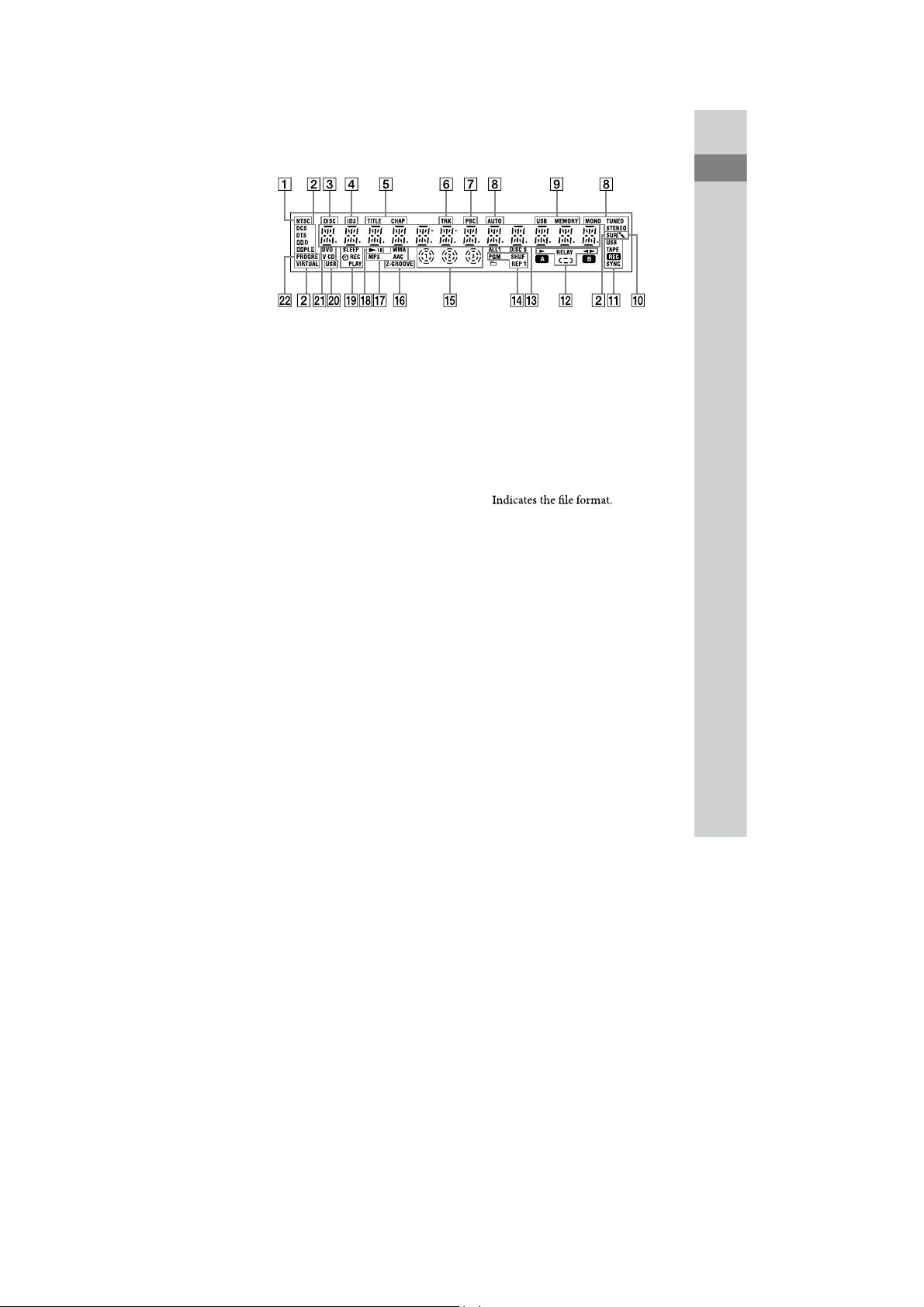
HCD-GZR7D/GZR8D/GZR9D
Guide to parts and controls
" Lights up when the output video
signal is NTSC. (27)
# Indicates the current surround
format.
$ Lights up when disc number is
displayed.
% Lights up when the ID3 tag
information is displayed.
& Lights up when the title or chapter
number is displayed.
' Lights up when the track information
is displayed.
( Lights up when playing VIDEO CD
with PBC function. (42)
) Lights up in “TUNER” function. (71)
* Lights up when the USB device is
recognized. (85)
+ Lights up when the Karaoke Mode is
turned on. (98)
, Lights up during transfer or
recording. (75, 78, 83)
- Indicates the tape playback direction.
(74)
. Displays the text information.
/ Indicates the selected play mode. (44)
0 Indicates the disc presence. (38)
1 Lights up when “GROOVE” or “Z-
GROOVE” is turned on. (94)
2
3 Indicates the playback status of the
disc or USB device.
4 Lights up when the timer is set. (105)
5 Lights up when the “USB” function is
selected. (85)
6 Indicates the type of disc being played
back. (38)
7 Lights up when “PROGRESSIVE
(COMPONENT OUT)” is set to
“ON.” (28)
19
GB
15
Page 16
HCD-GZR7D/GZR8D/GZR9D
Hooking up optional
components
To enhance your system, you can connect
optional components. Refer to the
operating instructions provided with
each component.
Rear panel
MHC-GZR9D
MHC-GZR8D
MHC-GZR7D
Other Operations
Continued
M
113
GB
16
Page 17

HCD-GZR7D/GZR8D/GZR9D
"
VIDEO/SAT AUDIO IN L/R jacks
Connect the audio output jacks of an
optional component (such as VCR or
satellite tuner).
#
VIDEO/SAT VIDEO IN jack
Connectthevideooutputjackofan
optional component (such as VCR or
satellite tuner).
$
COMPONENT VIDEO OUT jacks
Connect the component video input
jacks of the TV or projector. If your
TV accept progressive format signals,
you must use this connection and set
“PROGRESSIVE (COMPONENT
OUT)” to “ON” (page 28). You can
enjoy higher quality video images.
Note
You cannot output the video signal
from the VIDEO/SAT VIDEO IN
jack through the COMPONENT
VIDEO OUT jacks of this unit.
%
VIDEO OUT jack
Connect the video input jack of the
TV or projector.
&
S VIDEO OUT jack
Connect the S Video input jack of the
TV or projector. You can enjoy higher
quality video images when you select
the S VIDEO.
Note
You cannot output the video signal
from the VIDEO/SAT VIDEO IN
jack through the S VIDEO OUT jack
of this unit.
'
DMPORT (DIGITAL MEDIA
PORT)
Connect the DIGITAL MEDIA PORT
adapter (not supplied). You need to
connect the DIGITAL MEDIA PORT
adapter to an optional audio device
(portable audio player, etc.).
Notes
Available DIGITAL MEDIA PORT
adapters vary in each area.
Do not connect an adapter other than the
DIGITAL MEDIA PORT adapter.
Do not connect or disconnect the
DIGITAL MEDIA PORT adapter to/from
the DMPORT while the system is on.
When using a DIGITAL MEDIA PORT
adapter (not supplied) that has video
output function, connect the adapter
directlytotheTV.
114
GB
17
Page 18
HCD-GZR7D/GZR8D/GZR9D
(
D-LIGHT SYNC OUT jack
(Except for Russian and
Australian models)
Connect the D-LIGHT SYNC
controller (not supplied). You need
to connect the D-LIGHT SYNC
controller to the lighting device* (not
react according to control signals
transmitted by the D-LIGHT SYNC
controller upon receiving music
source from the system. For details
on the use of D-LIGHT SYNC
controller and lighting device, refer to
the respective operating instructions
supplied with the respective device.
* Refer to the D-LIGHT SYNC
controller operating instruction for the
recommended lighting device.
Note
depending on the connected lighting
device or the type of music being played
back.
)
SUBWOOFER OUT jack (MHCGZR8D/GZR7D only)
Connect the audio input jack of an
optional subwoofer*.
* SA-GNV111D is recommended. In some
areas, the SA-GNV111D may not yet be
available.
Note
occur depending on the connected
subwoofer or the type of music being
played back.
*
DVD DIGITAL OUT jack (MHCGZR7D only)
Connect the digital optical input jack
of an optional digital component
5.1 channel sound, if the connected
or DTS decoder.
Notes
Sound is output only when the system
functionissetto“DVD”or“USB.”
If you press AUDIO
(
orthebuttonsrelatedtoKaraoke
Mode, or if you connect or disconnect
microphones or headphones, the sound
6
, SOUND FIELD
Other Operations
Continued
M
115
GB
18
Page 19
DISASSEMBLY
• This set can be disassembled in the order shown below.
SET
HCD-GZR7D/GZR8D/GZR9D
SECTION 3
3-1. CASE
(Page 20)
3-2. LOADING PANEL
(Page 20)
3-3. TUNER PACK,
DMPORT BOARD
(Page 21)
3-4. DVD BLOCK SECTION
(Page 21)
3-5. FRONT PANEL SECTION
(Page 22)
3-13. TAPE MECHANISM DECK
(Page 26)
3-19. VIDEO BOARD
(Page 29)
3-20. DMB18 BOARD
(Page 29)
3-23. DRIVER BOARD,
SW BOARD
(Page 31)
3-21. DVD ASSY
(Page 30)
3-22. OPTICAL PICK-UP
(Page 30)
3-24. SENSOR BOARD
(Page 31)
3-25. MOTOR (TB) BOARD
(Page 32)
3-26. MOTOR (LD) BOARD
(Page 32)
3-14. MIC BOARD,
HEADPHONE BOARD
(Page 26)
3-15. LID (TC-L),
LID (TC-R)
(Page 27)
3-16. PANEL BOARD,
VOLUME BOARD,
KEY-RIGHT BOARD
(Page 27)
3-17. USB BOARD
(Page 28)
3-18. KEY-LEFT BOARD
(Page 28)
3-6. SUB-TRANS BOARD
(Page 22)
3-7. BACK PANEL SECTION
(Page 23)
3-8. BOARDS SECTION
(Page 23)
3-9. SURR & CENT AMP BOARD
(HCD-GZR8D/GZR9D)
(Page 24)
3-10. MAIN BOARD
(Page 24)
3-11. REGULATOR BOARD
(Page 25)
3-12. AMP FR & SW BOARD
(Page 25)
19
Page 20
HCD-GZR7D/GZR8D/GZR9D
Note: Follow the disassembly procedure in the numerical order given.
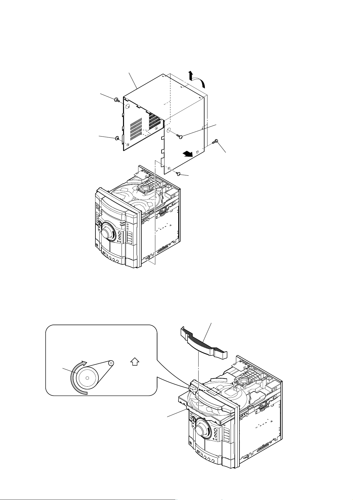
3-1. CASE
screw
(case 3 TP2)
screw
(case 3 TP2)
case
screw
(case 3 TP2)
screw
(case 3 TP2)
seven screws
(+BVTP 3 × 8)
3-2. LOADING PANEL
CD mechanism deck (CDM74)
Turn the pulley to the direction of the arrow.
pulley
Front panel side
Pull-out the disc tray.
loading panel
20
Page 21
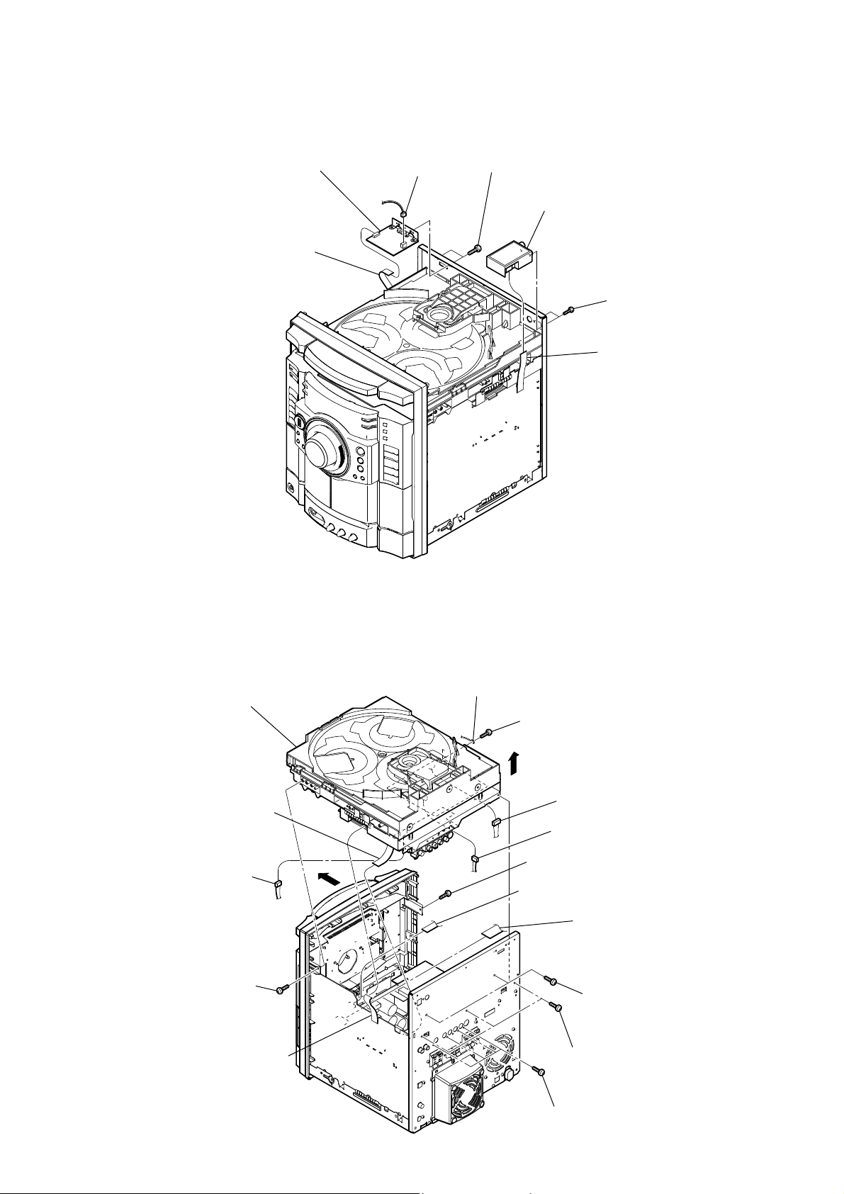
3-3. TUNER PACK, DMPORT BOARD
HCD-GZR7D/GZR8D/GZR9D
DMPORT board
wire (flat type)(9 core)
(CN201)
CN203 (2P)
two screws
(+BVTP 3 × 8)
tuner pack
two screws
(+BVTP 3 × 6)
connector (9 core)
3-4. DVD BLOCK SECTION
RK DVD block section
RG wire (flat type)(9 core)
(CN502)
RE CN903 (3P)
screw
(+BVTP 3 × 8)
wire (flat type)(13 core)
(CN701)
RH
wire
screw
(+BVTP 3 × 8)
RI
RT CN401 (5P)
RB CN111 (3P)
screw
(+BVTP 3 × 8)
wire (flat type)(15 core)
(CN503)
wire (flat type)(21 core)(CN201)
(HCD-GZR8D/GZR9D)
wire (flat type)(23 core)(CN202)
(HCD-GZR7D)
two screws
(+BVTP 3 × 8)
three screws
(+BVTP 3 × 8)
four screws
(+BVTP 3 × 8)
21
Page 22

HCD-GZR7D/GZR8D/GZR9D
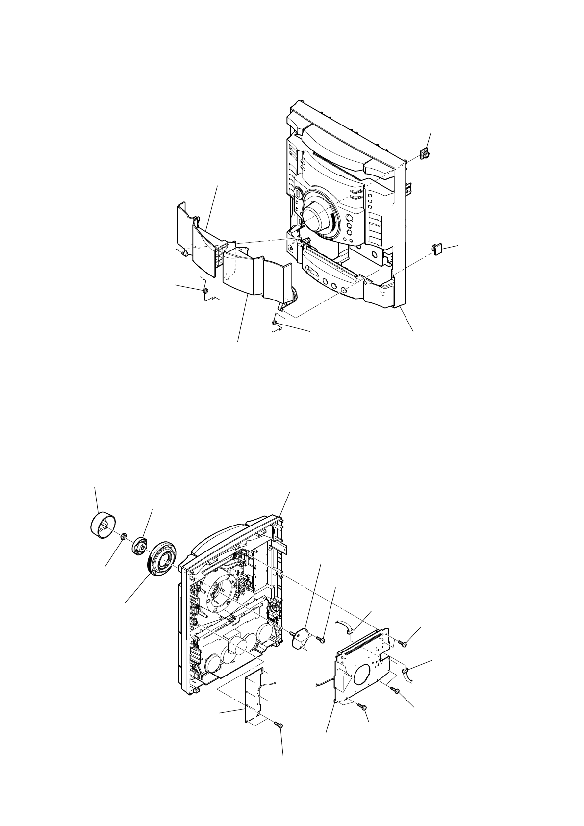
3-5. FRONT PANEL SECTION
front panel section
wire (flat type)(11 core)
(CN103)
CN073 (2P)
3-6. SUB-TRANS BOARD
CN901 (2P)
CN301 (3P)
CN302 (8P)
wire (flat type)(29 core)
(CN402)
wire (flat type)(9 core)
(CN101)
four screws
(+BVTP 3 × 8)
SUB-TRANS board
CN911 (4P)
three screws
(+BVTP 3 × 8)
22
Page 23

3-7. BACK PANEL SECTION
HCD-GZR7D/GZR8D/GZR9D
four screws
(+BVTP 3 × 8)
CN448 (4P)
(HCD-GZR9D)
CN447 (9P)
screw
(+BVTP 3 × 8)
five screws
(+BVTP 3 × 8)
CN602 (3P)
CN544 (6P)
(HCD-GZR8D/GZR9D)
back panel section
CN601 (3P)
3-8. BOARDS SECTION
boards section
screw
(+BVTP 3 × 6)
spring (EMC)
two screws
(+BVTP 3 × 8)
two screws
(+BV3 (3-CR))
two screws
(+BV3 (3-CR))
wire (flat type)(11 core)
(CN102)
CN443 (5P)
CN907 (11P)
23
Page 24

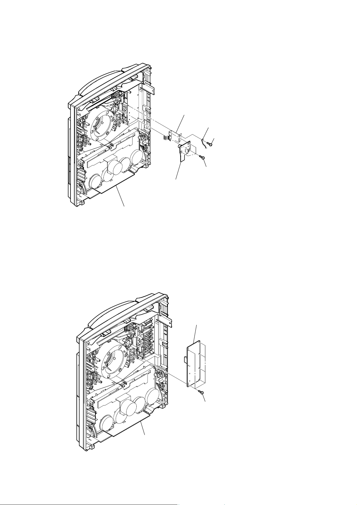
HCD-GZR7D/GZR8D/GZR9D
3-9. SURR & CENT AMP BOARD (HCD-GZR8D/GZR9D)
screw
(+BVTP 3 × 8)
duct (fan)
SURR & CENT AMP board
bracket (PWB AMP)
two screws
(+BVTP 3 × 8)
two screws
(transister)
CN444 (7P)
screw
(+BVTP 3 × 8)
3-10. MAIN BOARD
MAIN board
screw
(+BVTP 3 × 8)
AMP FR & SW board
REGULATOR board
24
Page 25
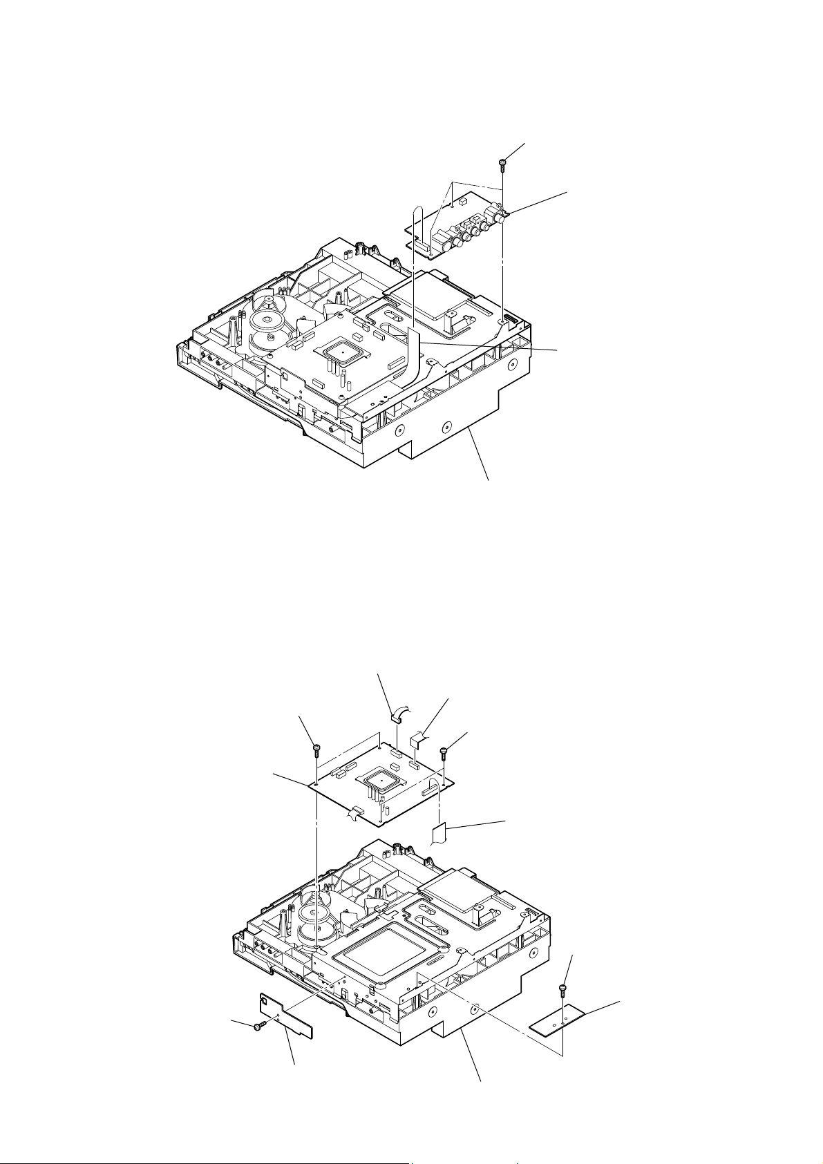
3-11. REGULATOR BOARD
HCD-GZR7D/GZR8D/GZR9D
four screws
(+BVTP 3 × 8)
REGULATOR board
AMP FR & SW board
3-12. AMP FR & SW BOARD
bracket (PWB AMP-B)
screw
(+BVTP 3 × 8)
bracket (PWB AMP)
screw
(+BVTP 3 × 8)
two screws
(transister)
screw
(+BVTP 3 × 8)
screw
(+BVTP 3 × 8)
AMP FR & SW board
screw
(+BVTP 3 × 8)
AMP HLDR board
heat sink assy
25
Page 26
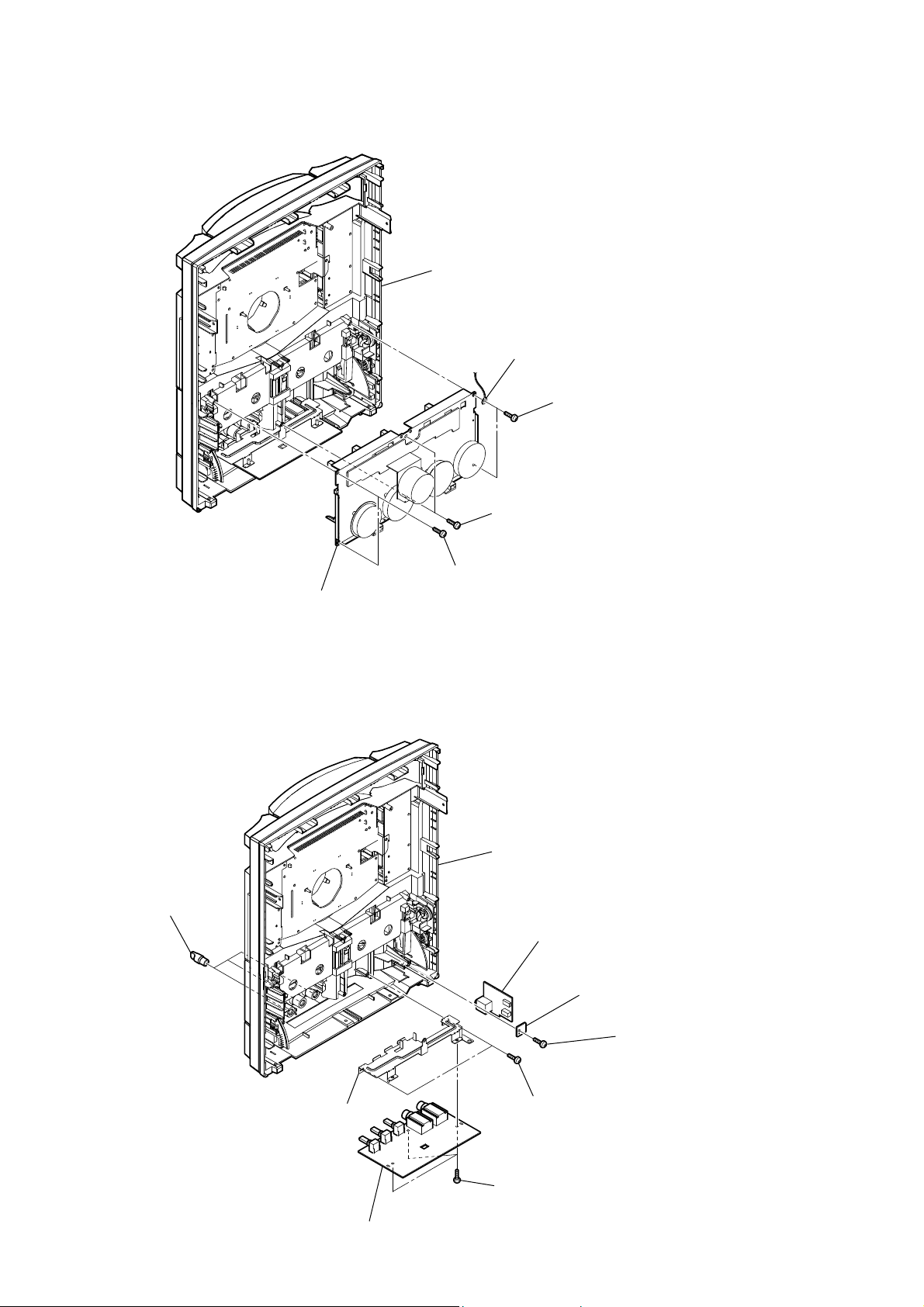
HCD-GZR7D/GZR8D/GZR9D
3-13. TAPE MECHANISM DECK
front panel assy
wire
two screws
(+BVTP 2.6 (3CR))
tape mechanism deck
3-14. MIC BOARD, HEADPHONE BOARD
three knobs (MIC)
two screws
(+BVTP 2.6 (3CR))
two screws
(+BVTP 2.6 (3CR))
front panel assy
HEADPHONE board
26
holder (MIC PWB)
HP HLDR board
screw
(+BVTP 2.6 (3CR))
two screws
(+BVTP 2.6 (3CR))
three screws
(+BVTP 2.6 (3CR))
MIC board
Page 27
3-15. LID (TC-L), LID (TC-R)
spring (TC-L)
HCD-GZR7D/GZR8D/GZR9D
damper
lid (TC-L)
damper
spring (TC-R)
lid (TC-R)
3-16. PANEL BOARD, VOLUME BOARD, KEY-RIGHT BOARD
knob (VOL)
holder (JOG)
nut
knob (JOG)
front panel assy
RG VOLUME board
RE three screws
(+BVTP 2.6 (3CR))
front panel assy
RB CN606 (3P)
two screws
(+BVTP 2.6 (3CR))
KEY-RIGHT board
PANEL board
seven screws
(+BVTP 2.6 (3CR))
RT CN608 (3P)
(HCD-GZR7D/GZR8D)
CN607 (5P)
(HCD-GZR9D)
three screws
six screws
(+BVTP 2.6 (3CR))
(+BVTP 2.6 (3CR))
27
Page 28
HCD-GZR7D/GZR8D/GZR9D
3-17. USB BOARD
plate (USB) ground
wire
screw
(+BVTP 2.6 (3CR))
three screws
(+BVTP 2.6 (3CR))
USB board
3-18. KEY-LEFT BOARD
front panel assy
KEY-LEFT board
28
six screws
(+BVTP 2.6 (3CR))
front panel assy
Page 29
3-19. VIDEO BOARD
HCD-GZR7D/GZR8D/GZR9D
three screws
(+BVTP 3 × 8)
VIDEO board
wire (flat type)(15 core)
(CN901)
3-20. DMB18 BOARD
DMB18 board
two screws
(+BVTP 3 × 8)
DVD mechanism block
CN201 (6P)
wire (flat type)(24 core)
(CN101)
two screws
(+BVTP 3 × 8)
wire (flat type)(21 core)(CN304)
(HCD-GZR8D/GZR9D)
wire (flat type)(23 core)(CN302)
(HCD-GZR7D)
screw
(+BVTP 3 × 8)
screw
(+BVTP 3 × 8)
FFC HLDR3 board
FFC HLDR2 board
DVD mechanism block
29
Page 30
HCD-GZR7D/GZR8D/GZR9D
3-21. DVD ASSY
FFC HLDR3 board
cover (CDM) section
screw
(+BVTP 3 × 8)
CN201 (6P)
screw
(+BVTP 3 × 8)
screw
(+BVTP 3 × 8)
screw
(+BVTP 3 × 8)
screw
(+BVTP 3 × 6)
spring (EMC)
wire (flat type)(24 core)
(CN101)
RB floating screw
(+PTPWH M2.6)
RT DVD assy
3-22. OPTICAL PICK-UP
two insulator screws
optical pick-up
DVD mechanism section
two insulators
two insulator screws
two insulators
30
holder (310)
Page 31

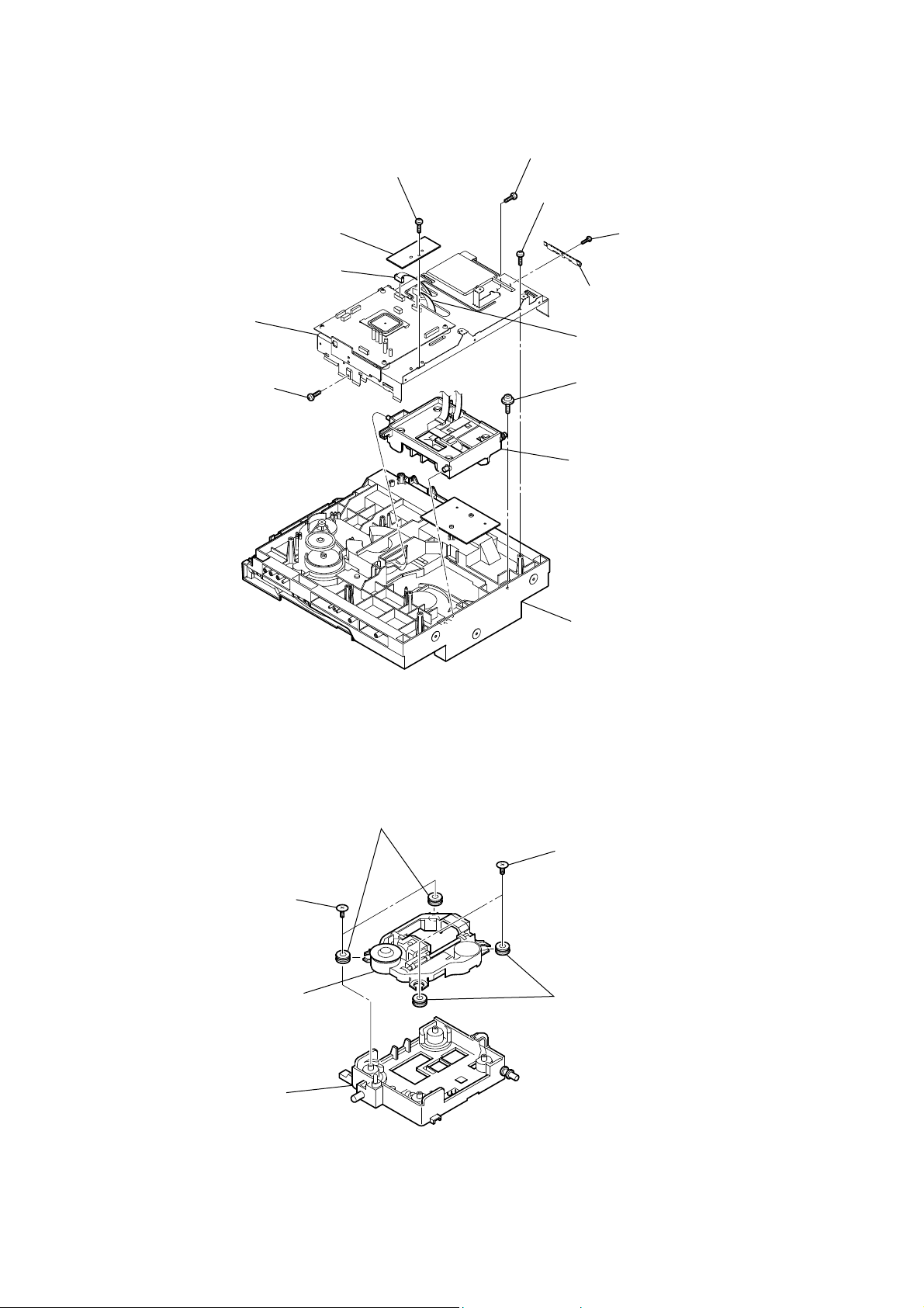
3-23. DRIVER BOARD, SW BOARD
HCD-GZR7D/GZR8D/GZR9D
CN702 (5 core)
CN703 (4P)
SW board
3-24. SENSOR BOARD
tray
screw
(+BTTP (M2.6))
floating
(+PTPWH M2.6)
screw
screw
(+BTTP (M2.6))
CN704 (2P)
SENSOR board
DRIVER board
two
screws
(+BTTP (M2.6))
belt (table)
floating
(+PTPWH M2.6)
pulley (table)
screw
floating
(+PTPWH M2.6)
screw
gear (geneva)
CN731
(3P)
31
Page 32

HCD-GZR7D/GZR8D/GZR9D
3-25. MOTOR (TB) BOARD
table assy
stopper
stopper
table motor assy (M741)
3-26. MOTOR (LD) BOARD
Remove the two solders of motor.
loading motor assy (M751)
MOTOR (TB) board
Remove the two solders of motor.
two
screws
(+BTTP (M2.6))
two
screws
(+BTTP (M2.6))
MOTOR (LD) board
32
belt (loading)
Page 33

SECTION 4
TEST MODE
HCD-GZR7D/GZR8D/GZR9D
[COLD RESET]
• The cold reset clears all data including preset data stored in the
RAM to initial conditions. Execute this mode when returning
the set to the customer.
Procedure:
1. Press the [
2. Press [ILLUMINATION] button, [ENTER] button and [
button simultaneously.
3. The message “COLD RESET” appears on the fl uorescent
indicator tube. Then, the fl uorescent indicator tube becomes
blank for a while, and the system is reset.
[COMMON TEST MODE]
• This mode is used to check operations of the respective section
of Equalizer level, volume and VACS ON/OFF.
Procedure:
• To enter Common Test Mode
1. Press [
2. Press [x] button, [ILLUMINATION] button and [DISC 3]
simultaneously.
3. The message “VACS0” appers on the fl uorescent indicator
tube.
• Check of Equalizer Level
1. Press [EQ BAND/MEMORY] button repeatedly until a
message “ALL EQ MIN” appears on the fl uorescent indicator
tube. GEQ decreases to its minimum.
2. Press [EQ BAND/MEMORY] button repeatedly until a
message “ALL EQ MAX” appears on the fl uorescent
indicator tube. GEQ increases to its maximum.
3. Press [EQ BAND/MEMORY] button repeatedly until a
message “ALL EQ FLAT” appears on the fl uorescent
indicator tube. GEQ is set to fl at.
• Check of Volume
1. When the [MASTER VOLUME] dial is turned
counterclockwise even slightly, the sound volume increases
to its maximum and message “VOLUME16” t “VOLUME
MAX” appears on the fl uorescent indicator tube.
2. When the [MASTER VOLUME] dial is turned clockwise
even slightly, the sound volume decreases to its minimum and
message “VOLUME16” t “VOLUME MIN” appears on the
fl uorescent indicator tube.
• Check of VACS (Variable Attenuation Control System)
ON/OFF Select
1. Press [REC TO TAPE] button repeatedly until a message
“VACS OFF” or “VACS ON” appears on the fl uorescent
indicator tube.
• To release from Common Test Mode
1. To release from this mode, press [
2. To cold reset is enforced at the same time.
] button to turn on the system.
?/1
] button to turn on the system.
?/1
?/1
?/1
] button.
[AMP TEST MODE]
• This mode is used to display the real time VACS level and
check operations of the respective sections of Equalizer band
and DBFB ON/OFF.
Procedure:
• To enter AMP Test Mode
1. Press [
]
2. Press [x] button, [EQ BAND/MEMORY] button and [REC
TO USB] button simultaneously.
3. The message “AMP TEST IN” appers of the fl uorescent
indicator tube.
• Check of VACS Display/AMP Adjustment Select
1. Press [REC TO TAPE] button repeatedly until a message
“V0 0 0” appears on the fl uorescent indicator tube. “0”
represents VACS level which is triggered by signal level.
2. Press [REC TO TAPE] button repeatedly until a message
“D +6 +2 +4” appears on the fl uorescent indicator tube. “+6”
represents Equalizer Low level, “+2” represents Equalizer
Mid level and “+4” represents Equalizer High level.
• Check of Equalizer Band Select
1. Press [EQ BAND/MEMORY] button repeatedly until a
message “LOW +6 dB” appears on the fl uorescent indicator
tube. EQ Band is set to Low level.
2. Press [EQ BAND/MEMORY] button repeatedly until a
message “MID +2 dB” appears on the fl uorescent indicator
tube. EQ Band is set to Middle level.
3. Press [EQ BAND/MEMORY] button repeatedly until a
message “HIGH +4 dB” appears on the fl uorescent indicator
tube. EQ Band is set to High level.
• Change of Equalizer Band
1. Press [EQ BAND/MEMORY] button repeatedly until a
message “LOW +6 dB” appears on the fl uorescent indicator
tube.
2. When the [OPERATION DIAL] ring is turned clockwise or
counterclockwise even slightly, “LOW +6 dB” change to
“LOW –8 dB” y “LOW +8 dB” appears on the fl uorescent
indicator tube.
3. Press [EQ BAND/MEMORY] button repeatedly until a
message “MID +2 dB” appears on the fl uorescent indicator
tube.
4. When the [OPERATION DIAL] ring is turned clockwise
or counterclockwise even slightly, “MID +2 dB” change to
“MID –8 dB” y “MID +8 dB” appears on the fl uorescent
indicator tube.
5. Press [EQ BAND/MEMORY] button repeatedly until a
message “HIGH +4 dB” appears on the fl uorescent indicator
tube.
6. When the [OPERATION DIAL] ring is turned clockwise or
counterclockwise even slightly, “HIGH +4 dB” change to
“HIGH –8 dB” y “HIGH +8 dB” appears on the fl uorescent
indicator tube.
] button to turn on the system.
?/1
• Check of DBFB ON/OFF Select
1. Press [OPTIONS] button repeatedly until a message “DBFB
OFF” or “DBFB ON” appears on the fl uorescent indicator
tube.
• To release from AMP Test Mode
1. To release from this mode, press [x] button, [EQ BAND/
MEMORY] button and [
] button simultaneously.
?/1
33
Page 34

HCD-GZR7D/GZR8D/GZR9D
[TCM OFFLINE MODE]
• This mode prevents the system from tuning off automatically
when TCM is not connected. Therefore, measurements can be
done even when TCM is not connected during production.
Procedure:
1. Press [
] button to turn on the system.
?/1
(SONY DEMO mode)
2. Press [SOUND FIELD] button, [EQ BAND/MEMORY]
button and [
] button simultaneously. The system will turn
?/1
on automatically.
3. The message “TCM OFFLINE” appers on the fl uorescent
indicator tube.
• To release from TCM OFFLINE Mode
1. To release from this model, press [
?/1
] button.
[PANEL TEST MODE]
• This mode is used to check the fl uorescent indicator tube,
LEDs, button, MASTER VOLUME dial OPERATION DIAL
ring, system software version, DVD lib version, model name
and destination.
Procedure:
1. Press [
] button to turn on the system.
?/1
2. Press [x] button, [ILLUMINATION] button and [DISC 2]
button simultaneously.
3. Power illuminator LEDs and segment in fl uorescent indicator
tube are lighted up.
4. When you want to enter to the system software version
display model, press [DISC 1] button. The system software
version appears on the fl uorescent indicator tube.
Press [DISC 1] button again, the DVD lib version appears on
the fl uorescent indicator tube.
5. Press [DISC 2] button the key encode test mode is activated.
6. In the key encode test mode,the fl uorescent indicator tube
displays “KEY 0 0 0 0”.
Each time a button pressed, cange the each numbers.
7. Press [DISC 3] button the mode name and destination on the
fl uorescent indicator tube.
• To release from Panal Test Mode
1. To release from this mode, press [x] button,
[ILLUMINATION] button and [DISC 2] button
simultaneously.
[DVD SHIP MODE (WITHOUT MEMORY CLEAR)]
• This mode moves the optical pick-up to the position durable to
vibration. Use this mode when returning the set to the customer
after repair.
Procedure:
1. Press [
] button to turn on the system.
?/1
2. Press [DVD] button, to set the “DVD NO DISC” mode.
3. press [
] button and [
Y
] button simultaneously.
?/1
The system will turn off automatically.
4. After the “STANDBY” blinking display fi nishes, a message
“LOCK” appears on the fl uorescent indicator tube and the
DVD ship mode is set.
[DVD SHIP MODE (WITHOUT MEMORY CLEAR)]
• This mode moves the optical pick-up to the position durable
to vibration and clears all data including preset data stored in
the RAM to initial conditions after the power supply is turned
off. Use this mode when returning the set to the customer after
repair.
Procedure:
1. Press [
] button to turn on the system.
?/1
2. Press [DVD] button, to set the “DVD NO DISC” mode.
3. press [ENTER] button, [GROOVE] button and [
?/1
] button
simultaneously.
4. After the “STANDBY” blinking display fi nishes, a message
“COLD RESET” appears on the fl uorescent indicator tube
and the DVD ship mode is set.
• To release from DVD Ship Mode
1. To release from this model, press [
?/1
] button.
[DISC THEFT PREVENTION MODE]
• This mode let you lock the disc tray. When this mode is
activated, the disc tray will not open.
Procedure:
1. Press [
] button to turn on the system.
?/1
2. Press [DVD] button.
3. Press [x] button and [Z OPEN/CLOSE] button
simultaneously and hold down until “LOCKED” or
“UNLOCKED” appers on the fl uorescent indicator tube
(around 5 seconds).
• To release from Disc Theft Prevention Mode
1. To release from this model, press [
?/1
] button.
[DVD COLOR SYSTEM MODE]
• This mode let you change the color system of the video output
from PAL to NTSC or vice-versa.
Procedure:
1. Press [
] button to turn on the system.
?/1
2. Press [DVD] button.
3. Press [
4. Press [X] button and [
] button to turn off the system.
?/1
] button simultaneously.
?/1
The system will turn off automatically.
5. The message “COLOR PAL” or “COLOR NTSC” appears on
the fl uorescent indicator tube.
• To release from DVD Color System Mode
1. To release from this model, press [
?/1
] button.
[DVD FIRMWARE VERSION MODE]
• This mode is used to display the DVD fi rmware version.
Procedure:
1. Press [
] button to turn on the system.
?/1
2. Press [DVD] button.
3. Press [
] button and [
x
] button simultaneously.
?/1
4. The version of DVD fi rmware appears on the on-screen
display on TV.
• To release from DVD Ship Mode
1. To release from this model, press [
34
?/1
] button.
• To release from DVD Firmware Version Mode
1. To release from this mode, press [
?/1
] button.
Page 35

HCD-GZR7D/GZR8D/GZR9D
[DVD REBOOT AVOIDANCE MODE]
• This mode is used to display the DVD Reboot Avoidance.
Procedure:
1. Press [
] button to turn on the system.
?/1
2. Press [DVD] button.
3. Press [DVD] button, [x] button and [DISC 3] button
simultaneously.
4. The message “MTK DBG” appears on the fl uorescent
indicator tube.
• To release from DVD Reboot Avoidance Mode
1. To release from this mode, press [
?/1
] button.
[AM TUNER STEP CHAGE]
• The step interval of AM channels can be toggled between 9
kHz and 10 kHz.
Procedure:
1. Press [
] button to turn off the system.
?/1
2. Press [TUNER/BAND] button repeatedly to select the “AM”.
3. Press [
4. Press [TUNING +] button and [
] button to turn on the system.
?/1
] button simultaneously.
?/1
The system will turn on automatically.
5. The message “AM 9k STEP” or “AM 10k STEP” appears
on the fl uorescent indicator tube and thus the channel step
change.
[VIDEO/SAT FUNCTION CHANGE]
• This mode let you change from VIDEO to SAT and vice-versa.
Procedure:
1. Press [
] button to turn on the system.
?/1
2. Press [VIDEO/SAT] button.
3. Press [VIDEO/SAT] button and [
] button simultaneously.
?/1
The function will change to SAT. Press the same button again
to change from SAT to VIDEO.
[DVD SERVICE MODE]
• This mode let you make diagnosis and adjustment easily by
using the remote commander and the TV. The instructions,
diagnostic results, etc. are given on the on-screen display.
• TEST DISC LIST
Be sure to use the DVD disc that matches the signal standards of
your region.
• CD
YEDS-18 (Part No.: 3-702-101-01)
PATD-012 (Part No.: 4-225-203-01)
• DVD SL (Single Layer)
NTSC : HLX-503 (Part No.: J-6090-069-A)
HLX-504 (Part No.: J-6090-088-A)
PAL : HLX-506 (Part No.: J-6090-077-A)
• DVD DL (Dual Layer)
NTSC : HLX-501 (Part No.: J-6090-071-A)
HLX-505 (Part No.: J-6090-089-A)
PAL : HLX-507 (Part No.: J-6090-078-A)
• Procedure to enter to DVD Service Mode:
1. Press [
] button to turn on the system.
?/1
2. Press [DVD] butoon.
3. Press [
] button and [Z OPEN/CLOSE] button
x
simultaneously and then turn the [MASTER VOLUME] dial
clockwise.
4. The message “SERVICE IN” appears on the fl uorescent
indicator tube and the Top Menu of Remocon Diagnosis
Menu appears on the on-screen display on the TV. The model
name, main unit’s micom version information (IF-con) and
DVD fi rmware version information (Syscon) are displayed at
the bottom of the on-screen display.
Remocon Diagnosis Menu
0. External Chip Check
1. Servo Parameter Check
2. Drive Manual Operation
3. Emergency History
4. Version Information
Model Name
IF-con
Syscon
: SSX2D_ME
: Ver. 01.00 (0000)
: Ver. 1.200
5. To execute each function, press its number by using numeric
button on the remote commander.
6. To release from this mode, press [
] button to turn off the
?/1
system.
• Execute IOP Measurement
In order to execute IOP measurement, the following standard
procedures must be followed.
1. From the Top Menu of Remocon Diagnosis Menu, select “2.
Drive Manual Operation” by pressing the [2] button on the
remote commander. The following screen appears on the onscreen display.
Drive Manual Operation
1. Servo Control
2. Track/Layer Jump
3. Manual Adjustment
4. Mecha test mode
5. MIRR time Adjust
0. Return to Top Menu
2. Select “3. Manual Adjustment” by pressing the [3] button on
the remote commander. The following screen appears on the
on-screen display.
Manual Adjust
1. Track Balance Adjust:
2. Track Gain Adjust:
3. Focus Balance Adjust:
4. Focus Gain Adjust:
5. Eg Boost Adjust:
6. Iop:
7. TRV. Level:
8. S curve (FE) Level:
9. RFL (PI) Level:
0. MIRR Time:
0P Change Value
RETURN Return to previous menu
35
Page 36

HCD-GZR7D/GZR8D/GZR9D
3. Select “6. Iop:” by pressing [6] button on the remote
commander.
4. Wait until a hexadecimal number appears in the on-screen
display as below:
Manual Adjust
1. Track Balance Adjust:
2. Track Gain Adjust:
3. Focus Balance Adjust:
4. Focus Gain Adjust:
5. Eg Boost Adjust:
6. Iop. ED
7. TRV. Level:
8. S curve (FE) Level:
9. RFL (PI) Level:
0. MIRR Time:
0P Change Value
RETURN Return to previous menu
5. Convert data from hexadecimal to decimal by using
conversion table.
6. Please fi nd the label on the rear of the BU (Base Unit).
The default IOP value is written in the label.
7. Subtract between these two values.
8. If the remainder is smaller than 93 (decimal), then it is OK.
However if the value is higher than 93, then the BU is
defective and need to be change.
9. Press [RETURN] button on the remote commander to return
to previous menu.
10. Press [0] button on the remote commander to return to the
Top Menu of Remocon Diagnosis Menu.
11. Press [
] button to turn off the system.
?/1
• Error Code
Example of Error code
1. 01 05 04 04 00 92 46 00
00 00 00 00 00 00 23 45
The meaning of error code is as below:
01: Communication error (No reply from syscon)
02: Syscon hung up
03: Power OFF request when syscon hung up
19: Thermal shutdown
24: MoveSledHome error
25: Mechanical move error (5 Changer)
26: Mechanical move stack error
30: DC motor adjustment error
31: DPD offset adjustment error
32: TE balance adjustment error
33: TE sensor adjustment error
34: TE loop gain adjustment error
35: FE loop gain adjustment error
36: Bad jitter after adjustment
40: Focus NG
42: Focus layer jump NG
52: Open kick spindle error
51: Spindle stop error
60: Focus on error
61: Seek fail error
62: Read Q data/ID error
70: Lead in data read fail
71: TOC read time out (CD)
80: Can’t buffering
81: Unknown media type
• Check Emergency History
To check the emergency history, please follow the following
procedure.
1. From the Top Menu of Remocon Diagnosis Menu, select “3.
Emergency History” by pressing the [3] button on the remote
commander. The following screen appears on the on-screen
display.
Emg. History Check
Laser Hours CD 999h 59min
1. 01 05 04 04
00 00 00 00
2. 02 02 01 01 00 A9 4B 00
00 00 00 00
Next Next Page Prev Prev Page
O Return to Top Menu
DVD 999h 59min
00 92 46 00
00 00 23 45
00 00 23 45
2. You can check the total time when the laser is turned on
during playback of DVD and CD from the above menu. The
maximum time, which can be displayed are 999h 59min.
3. You can check the error code of latest 10 emergency history
from the above menu. To view the previous or next page
of emergency history, press [.] or [>] on the remote
commander. The error code consists of
• Parameter of error code
This is the detail of error code.
Example of Error code
1. 01 05 04 04 00 92 46 00
00 00 00 00 00 00 23 45
• Time of error code
This is the laser time when an error occurred.
Example of Error code
1. 01 05 04 04 00 92 46 00
00 00 00 00 00 00 23 45
To clear the Laser Hours
Press [ DISPLAY] button and then press [CLEAR] button. The
data for both CD and DVD data are reset.
Emg. History Check
Laser Hours CD 0h 0min
1. 01 05 04 04
00 00 00 00 00 00 23 45
2. 02 02 01 01 00 A9 4B 00
00 00 00 00 00 00 23 45
Next Next Page Prev Prev Page
O Return to Top Menu
DVD 0h 0min
00 92 46 00
36
Page 37

To clear the Emergency History
Press [DVD TOP MENU] button and then press [CLEAR] button.
The error code for all emergency history would be reset.
Emg. History Check
HCD-GZR7D/GZR8D/GZR9D
Laser Hours CD 999h 59min
1. 00 00 00 00
00 00 00 00
2. 00 00 00 00 00 00 00 00
00 00 00 00 00 00 00 00
Next Next Page Prev Prev Page
O Return to Top Menu
DVD 999h 59min
00 00 00 00
00 00 00 00
To clear the Initialize Setup Data
Press [DVD/TUNER MENU] button and then press [CLEAR]
button on the remote commander.
Version information
Firm (Main) : Ver. xxxxx
Firm (Sub) : xxxxx
RISC : xxxxx
8032 : xxxxx
Audio DSP : xxxxx
Servo DSP : xxxxx
O Return to Top Menu
To return to the Top Menu of Remocon Diagnosis Menu
Press [0] button on the remote commander.
• Check Version Information
To check the version information, please follow the following
procedure.
1. From the Top Menu of Remocon Diagnosis Menu, select “4.
Version Information” by pressing the [4] button on the remote
commander. The following screen appears on the on-screen
display.
Emg. History Check
Laser Hours CD 999h 59min
Initialize setup data...
Next Next Page Prev Prev Page
O Return to Top Menu
DVD 999h 59min
To return to the Top Menu of Remocon Diagnosis Menu,
press [0] on the remote commander.
37
Page 38

HCD-GZR7D/GZR8D/GZR9D
SECTION 5
MECHANICAL ADJUSTMENTS
Precaution
1. Clean the following parts with a denatured alcohol-moistened
swab:
record/playback heads pinch rollers
erase head rubber belts
capstan idlers
2. Demagnetize the record/playback head with a head
demagnetizer.
3. Do not use a magnetized screwdriver for the adjustments.
4. After the adjustments, apply suitable locking compound to
the parts adjusted.
5. The adjustments should be performed with the rated power
supply voltage unless otherwise noted.
Torque Measurement
Mode Torque meter Meter reading
FWD CQ-102C
FWD
back tension
REV CQ-102RC
REV
back tension
FF/REW CQ-201B
FWD tension CQ-403A
REV tension CQ-403R
CQ-102C
CQ-102RC
3.06 N • m to 6.96 N • m
31 to 71 g • cm
(0.43 – 0.98 oz • inch)
0.19 N • m to 0.58 N • m
2 to 6 g • cm
(0.02 – 0.08 oz • inch)
3.06 N • m to 6.96 N • m
31 to 71 g • cm
(0.43 – 0.98 oz • inch)
0.19 N • m to 0.58 N • m
2 to 6 g • cm
(0.02 – 0.08 oz • inch)
6.96 N • m to 14.02 N • m
71 to 143 g • cm
(0.98 – 1.99 oz • inch)
9.80 N • m
100 g or more
(3.53 oz or more)
9.80 N • m
100 g or more
(3.53 oz or more)
38
Page 39

HCD-GZR7D/GZR8D/GZR9D
SECTION 6
ELECTRICAL ADJUSTMENTS
DVD SECTION
When the optical pick-up assy is replaced, perform the “Execute
IOP Measurement”.
Execute IOP Measurement (See page 35)
[TEST DISC LIST]
Be sure to use the DVD disc that matches the signal standards of
your region.
• CD
YEDS-18 (Part No.: 3-702-101-01)
PATD-012 (Part No.: 4-225-203-01)
• DVD SL (Single Layer)
NTSC : HLX-503 (Part No.: J-6090-069-A)
HLX-504 (Part No.: J-6090-088-A)
PAL : HLX-506 (Part No.: J-6090-077-A)
• DVD DL (Dual Layer)
NTSC : HLX-501 (Part No.: J-6090-071-A)
HLX-505 (Part No.: J-6090-089-A)
PAL : HLX-507 (Part No.: J-6090-078-A)
[RFMON Level Check]
Connection:
oscilloscope
DMB18 board
CN105 pin (RFMON)
CN105 pin (GND)
+
–
Checking Location: DMB18 board (Side A)
DMB18 BOARD (SIDE A)
IC102
IC101
IC201
CN110
CN105 pin
(RFMON)
IC104
CN401
CN105 pin
(GND)
TUNER SECTION
FM Tune Level Check
CN105
Procedure:
1. Connect an oscilloscope to CN105 pin 6 (RFMON) and
CN105 pin 3 (GND) on the DMB18 board.
2. Turn the power on.
3. Set the test disc (refer to the TEST DISC LIST) on the tray
and press [Y] button to playback.
4. Confi rm that oscilloscope waveform is clear and check
RFMON signal level is correct or not.
Note: A clear RFMON signal waveform means that the shape
“◊” can be clearly distinguished at the center of the
waveform.
RFMON signal waveform
VOLT/DIV: 200 mV
TIME/DIV: 500 nS
level: 0.58 ± 1.23 Vp-p (DVD)
0.57 ± 1.1 Vp-p (CD)
signal
generator
set
Procedure:
1. Turn on the set.
2. Input the following signal from signal generator to FM
antenna input directly.
Carrier frequency: A = 87.5 MHz, B = 98 MHz, C = 108 MHz
Deviation : 75 kHz
Modulation : 1 kHz
ANT input : 35 dBμ (EMF)
Note: Use 75 ohm coaxial cable to connect signal generator and
the set.
You cannot use video cable for checking.
Use signal generator whose output impedance is 75 ohm.
3. Set to FM tuner function and tune A, B and C signals.
4. Confi rm “TUNED” is lit on the display for A, B and C
signals.
When the selected station signal is received in good condition,
“TUNED” is displayed.
39
Page 40

HCD-GZR7D/GZR8D/GZR9D
VIDEO SECTION
Video Level Check (VIDEO BOARD)
Purpose
This adjustment is made to satisfy the NTSC standard, and if not
adjusted correctly, the brightness will be too large or small.
oscilloscope
75 Ω
set
+
–
J902
VIDEO OUT
Procedure:
1. Connect oscilloscope to VIDEO outjack.
2. Load a DVD reference disc playback.
3. Check the video signal level is 1.00±0.07Vp-p.
1.00 ± 0.07 Vp-p
(WHITE 100%)
DECK SECTION
0 dB = 0.775V
1. Demagnetize the record/playback head with a head
demagnetizer.
2. Do not use a magnetized screwdriver for the adjustments.
3. After the adjustments, apply suitable locking compound to
the parts adjust.
4. The adjustments should be performed with the rated power
supply voltage unless otherwise noted.
5. The adjustments should be performed in the order given in
this service manual. (As a general rule, playback circuit
adjustment should be completed before performing recording
circuit adjustment.)
6. The adjustments should be performed for both L-CH and
R-CH.
7. Switches and controls should be set as follows unless
otherwise specifi ed.
• Test Tape
Tape Signal Used for
P-4-A063 6.3 kHz, –10 dB Azimuth Adjustment
Record/Playback Head Azimuth Adjustment
DECK A DECK B
Note: Perform this adjustments for both decks
Procedure:
1. Mode: Playback
test tape
P-4-A063
(6.3 kHz, –10 dB)
MAIN board
IC101
pin XI (L-CH)
pin RM (R-CH)
level meter
+
MAIN board
IC101
pin U (GND)
–
2. Turn the adjustment screw and check output peaks. If the
peaks do not match for L-CH and R-CH, turn the adjustment
screw
so that outputs match within 1dB of peak.
output
level
within
1 dB
L-CH
peak
R-CH
peak
within
1 dB
screw
position
L-CH
peak
screw
position
R-CH
peak
40
Page 41

3. Mode: Playback
test tape
P-4-A063
(6.3 kHz, –10 dB)
L-CH
MAIN
board
IC101
R-CH
pin XI
pin U
L
R
pin RM
waveform of oscilloscope
oscilloscope
V
H
HCD-GZR7D/GZR8D/GZR9D
in phase
45° 90° 135° 180°
good wrong
4. After the adjustments, apply suitable locking compound to
the pats adjusted.
Adjustment Location: Playback Head (Deck A)
Record/Playback/Erase Head (Deck B)
forward
reverse
41
Page 42

HCD-GZR7D/GZR8D/GZR9D
• Circuit Boards Location
TRANS board
KEY-LEFT board
USB board
PANEL board
SECTION 7
DIAGRAMS
SUB-TRANS board
SP TERM(SURR,CENT,SW) board
(HCD-GZR8D/GZR9D)
SP-TERMINAL board
SURR & CENT AMP board
(HCD-GZR8D/GZR9D)
REGULATOR board
VOLUME board
KEY-RIGHT board
SW board
MOTOR (LD) board
MOTOR (TB) board
SENSOR board
AMP FR & SW board
MAIN board
DMPORT board
DMB18 board
VIDEO board
DRIVER board
42
HEADPHONE board
TC board
MIC board
Page 43

HCD-GZR7D/GZR8D/GZR9D
HCD-GZR7D/GZR8D/GZR9D
4343
7-1. BLOCK DIAGRAM – RF/SERVO Section –
: DVD (AUDIO)
: DVD (RF)
: DVD (DIGITAL)
• Signal Path
DETECTOR
10
6
7
8
9
14
13
18
17
256 1
DVDRFIP
DVDA
DVDB
DVDC
DVDD
TPI
TNI
MC
MD
C
D
LD01
MDI1
LD02
MSW
MDI2
OSP
OSN
CD/DVD RF AMP,
FOCUS/TRACKING ERROR AMP,
DVD SYSTEM PROCESSOR,
DIGITAL SERVO PROCESSOR
IC102 (1/2)
OPTICAL PICK-UP
BLOCK
2AXIS
DEVICE
FOCUS/
TRACKING
COIL
22
19
LIMITSW
53
21
20
36 48
43
37 1
LASER DRIVER
CONTROL
Q102 (2/2)
MEDIA SWITCH
CONTROL
Q101,103
LASER DRIVER
CONTROL
Q102 (1/2)
LASER
DIODE
(FOR CD)
LASER
DIODE
(FOR DVD)
FOCUS COIL
DRIVE
42
41
BUFFER
35 3
34 4
TRACKING COIL
DRIVE
32
37
41
36
40
29
35
FOCUS/TRACKING COIL DRIVER,
SPINDLE/SLED MOTOR DRIVER
IC201
27
28
SPINDLE MOTOR
DRIVE
MM
SPINDLE
46
47
FMO
FOO
DMO
TRO
VREFO
OP INP
39
IOPMON
FOO
RF
A
B
C
D
F
E
CD LD
PD
LIMIT
VR650
VR780
MSW
DVD LD
FCS+
FCS–
TRK+
VCC
TRK–
SP+
SP–
SL+
SL–
D
C
B
A
VREFO
VREFO
12
NB
B
11
NA
A
30
29
SLED MOTOR
DRIVE
MM
54
BUFFER
19
20
22
21
40
45
SYSTEM
CONTROL
IC401 (1/4)
98
IFCK
I-MTK-CLK
46
XIFCS
I-DVD-XIFS
43
108
PRST
O-MTK-MTRST
42
97
99
IFSDO
I-MTK-DATA
45
100
IFSDI
110
XIFBSY
KRMOD
O-MTK-IFBSY
41
I-DVD-KRMOD
39
O-MTK-DATA
44
TRO
FMO
FOO
DMO
TRO
10
13
FMO
DMO
157
MUTE123
158
MUTE
130
TSDM
213
O-MTK-MICREQ
40
MIC
208
SLED
Page 44

HCD-GZR7D/GZR8D/GZR9D
HCD-GZR7D/GZR8D/GZR9D
4444
DVD SYSTEM PROCESSOR
IC102 (2/2)
EEPROM
IC103
FLASH ROM
IC101
SDRAM
IC104
B
MAIN
SECTION
A
MAIN
SECTION
C
AUDIO
SECTION
AVDD3.3V
VDD1.8V
226
ASDAT0
206
ADIN
ASDAT1
ASDAT2
ASDAT3
215
SDPIF
65
SCL
SDA
RST
WE
OE
22-26,
29-35
HA0-HA21
HD0 – HD7
A1-A21
DATA & ADDRESS BUS
DATA & ADDRESS BUS
79,80,82-86,89 121-119,116,113,129-122 140,141,143,144,155-149
92,56-62,74-67,
91,63,64,75,87
HD0 – HD7 A0 – A21
HD0 – HD7
A0
2645
CE
12
RESET
WE
28OE11
A0 – A19DQ15/A-1
XROMCS
XWR
7876
XRD66XSYSRST
108
DQ0 – DQ7
DRCLK
CE
CE
RST
OE
38
DRCLK
RD0 – RD15
RA0 – RA11
RA0 – RA11
RD0 – RD15
136
RCS
19
RCS
133
RWE
16
RWE
135
RAS
18
RAS
134
CAS
17
CAS
DQM0
15
DQM0
DQM1
39
DQM1
CKE
37
CLKE
101
SCL
102
SDA
137
BA0
20
BA0
BA1
21
BA1
WE
29,31,33,35,38,40,42,44 25-16, 10 -1, 48
138 146 11 1 132 147
2,4,5,7,8,10,11,13,42,44,45,47,48,50,51,53
225
SL
RECA L
D/A CONVERTER
IC4602
A/D CONVERTER
IC3601
22
LOUT2
2
AINL
223
222
183
B/Cb/Pb
WIDE
RGB SEL/DSEL
189
C
191
Y
185
Y/G
182
R/Cr/Pr
187
C VBS
221
XRST
203
ACLK
DAC
204
ABCK
205
ALRCK
3
44
45
SDTI1
13
PDN
12
SCLK
11
MCLK
10
LRCK
9
SDTO
V
C
Y
YG
CR/R
CB/B
WIDE
DSEL
9
SDTI2
10
SDTI3
11
SDTI4
5
RSTB
1
MCLK
2
BICK
4
LRCK
7
SCL
8
3
SDA
20
FC
19
SW
18
LT
25
FL
OPTICAL
TRANSMITTER
DVD
DIGITAL OUT
OPTICAL
LOUT3
ROUT3
LOUT4
LOUT1
GZR7D
IC302
7
WP
112
EEWP
198
SCORE
214
210
209
XVOICE
XVOICE
SCORE
XTALI
XTALO
239
238
197
VBUS OE
VBUS OC
196
USB DP
USB DM
2
4
1
3
3
CN804
IC072
USB+5V
REG
IC075
USB +5V
DETECT
(USB)
2
1
USB DP
USB DM
USB+5V
1
4
5
IC105
+3.3V REG
+3.3V REG
+1.8V REG
VDD3.3V
SW+5V
3
1
IC110
SW+3.3V
4
5
IC107
RF+3.3V
UNREG11V
X101
27MHz
200
SCL
199
SDA
• Signal Path
: VIDEO
: COMPONENT VIDEO
: AUDIO
: DVD (RF)
: DVD (DIGITAL)
7-2. BLOCK DIAGRAM – VIDEO Section –
(Page 45)
(Page 45)
(Page 46)
Page 45

HCD-GZR7D/GZR8D/GZR9D
HCD-GZR7D/GZR8D/GZR9D
4545
7-3. BLOCK DIAGRAM – MAIN Section –
DLIGHT
AUDIO
SECTION
D
VIDEO
SECTION
B
AUDIO
SECTION
E
VIDEO
SECTION
A
1
21
3
2
9
22
15
16
28
26
27
29
31
45
4629
21
16
T001
HRPE901
REC/PB/ERASE
HEAD
(DECK B)
HP901
PB
HEAD
(DECK A)
REC/PB
HEAD
TAPE MECHANISM
DECK BLOCK
ERASE
HEAD
A-PHOTO
B-PHOTO
B-REC-REV
A-HALF
B-HALF
B-REC-FWD
CAP M+
R-CH
R-CH
R-CH
L-CH
R-CH
L-CH
15
567
43
42
44
52
37
1
24
57
76
77
62
58
4
23
4
1
6
2
27
26
21
20
18
16
2
6
10
25
12
9
14
313
59
11
12
30
23
26
9
8
27
28
36
41
18
17
19
14
6
10
1
3
2
8
7
6
5
B-SOL
A-SOL
CD-L
SAT/VIDEO-L
TUNER-L
CD-L
TAPE REC/PB AMP,SOUND CONTROL
IC101
SYSTEM CONTROL
IC401 (2/4)
RECAL
TONEOUTL
SWOUT
OUTL
PB1L
PB2L
RECA L
TONEOUT L
SW OUT
FL OUT
SOUND
D201
BUFFER
IC703 (2/2)
BUFFER
IC703 (1/2)
BUFFER
IC702
BUFFER
IC202
BUFFER
IC701
Q302
DVD9V
HP DET
SA2
SA1
DPLL/SURL
DATA
CLK
MIC
O-AUDIO-IC-DATA
O-AUDIO-IC-CLK
I-TU-DO
O-TU-DI
O-TU-CLK
O-TU-CE
I-TU-TUNE
O-TC-REC-MUTE
O-TC-REC/PB-SW
O-TC-REC-BIAS
O-TC-CAPM-CNT
O-TC-B-TRIG
O-VIDEO-MUTE
I-ILLUMINATION
I-VACS
O-VIDEO-SEL
I-DMP-DET
O-DMP-DATA
O-DVD-POWER
I-MIC/HP-DET
I-DMP-DATA
O-FRONT-A-MUTE
O-TC-A-TRIG
TC-A-SHUT
TC-B-SHUT
REC-REV
I-TC-STAT
TAPE-L
RECBL
DMPORT-L
DPL-L
CAPSTAN/
REEL MOTOR
CONTROL
Q103,105
SOLENOID A
CONTROL
Q107,916
SOLENOID B
CONTROL
Q104,106
BIAS OSC
Q453
MUTE
Q305
MUTE
Q405
MUTE
Q303
MUTE
Q301
MIC 1
LEVEL
RV851
MIC 2
LEVEL
RV852
VOL1
MIC2P
MIC1P
P0OUT
MCO
VOL2
MIC/ECHO LEVEL AMP
IC851
MIC SIGNAL
AMP
IC852
VOL3
ECHO
LEVEL
RV853
REC/PB
SWITCH
Q408
MUTE
Q252
FL,FR
MUTE
Q261
DBFB FEED
BACK AMP
Q128
POWER
CONTROL
Q303,304
D-LIGHT
+4.5V REG
Q301
D-LIGHT
SYNC OUT
J304
3
4
CN204
R-CH
R-CH
DMP+5V
Lch+
Lch-
Rch+
RchVBUS(5V)
VDIDEO(5V)
TXD
DET
RXD
13
14
11
12
2
4
5
6
7
VACS
CONTROL
Q101,102
V
C
Y
YG
WIDE
CB/B
DSEL
CR/R
CVBS IN
COMPONENT VIDEO/S VIDEO AMP
IC901
VIDEO SELECTOR
IC902
C-IN
Y-IN
CY-IN
S1
CB-IN
I/P
CR-IN
CVBS OUT
S-DC OUT
C OUT
Y OUT
MUTE1
MUTE2
CY OUT
CB OUT
CR OUT
REC MUTE
CONTROL
Q410
REC MUTE
Q409
PB AMP
IC301
REC AMP
IC401
Q454,455
+9V
74
75
5
60
FM 75Ω
COAXIAL
AM
J301
TM901
R-CH
L
R
R-CH
+9V
DO
DI
CL
CE
TUNE
RCH
LCH
+9V
DO
DI
CL
CE
TUNED
AUDIO IN
-2
-1
ANTENNA
MIC 1
J851
MIC 2
J852
VIDEO/SAT
VIDEO
OUT
J902
S VIDEO
OUT
Y
C
Y
-3
-2
-1
P
B/CB
PR/CR
J904
COMPONENT
VIDEO OUT
J901
DMPORT
DC5V 0.7A MAX
VIDEO/SAT
VIDEO IN
J903
SCORE
EXCEPT AUS MODEL
XVOICE
• Signal Path
• R-CH is omitted due to same as L-CH.
• Abbreviation
AUS: Australian model
: TAPE PLAY (DECK B)
: TUNER
: TAPE PLAY (DECK A)
: TAPE REC (DECK B)
: AUDIO
: VIDEO
: COMPONENT VIDEO
(Page 46)
(Page 46)
(Page 44)
(Page 44)
Page 46

HCD-GZR7D/GZR8D/GZR9D
HCD-GZR7D/GZR8D/GZR9D
4646
MAIN
SECTION
E
VIDEO
SECTION
C
DISPLAY/
POWER
SECTION
F
MAIN
SECTION
D
+
–
+
–
• Signal Path
: AUDIO
IC731
Q731
M751
(LOADING)
M741
(TABLE)
SYSTEM CONTROL
IC401 (3/4)
TABLE
ADDRESS
SENSOR
DISC TRAY
ADDRESS
DETECT
RE701
OPEN/CLOSE
DETECT
S751
CLOSE OPEN
IC701
LOADING
MOTOR
DRIVER
IC712
TABLE
MOTOR
DRIVER
SURROUND/CENTER
SPEAKER RELAY
CONTROL
Q402
MUTE
Q256,257
MUTE
Q253,255
PROTECT
Q504,505
OVERLOAD
DETECT
Q506,507
FRONT SPEAKER
RELAY SWITCH
Q615,617
RELAY
CONTROL
Q480
PROTECT
Q485-487
SUBWOOFER RELAY
CONTROL
Q403
RELAY
DRIVER
Q490
LED
DRIVER
Q607
THERMAL
DET
Q483,484
SUBWOOFER
MUTE
Q258,259
OVERLOAD
DET
Q441,443
OVERLOAD
DET
Q481,482
RELAY
CONTROL
Q488
MUTE
Q509
MUTE
Q489
PROTECT
Q401
POWER
CONTROL
Q607,608
FAN
DRIVE
Q604,616
FAN
DRIVE
Q601,603
FAN
CONTROL
Q605,606
FAN
CONTROL
Q613,614
FAN
PROTECT
Q609-611
FAN
DRIVE
Q612
GZR7D
15
SL EXT IN
SW IN
R-CH
CD-L
DPL-L
SW OUT
HP DET
SOUND
FL OUT
TONE OUT L
RECA L
FL
SL
O-DVD-POWER
PROTECT
UNREG15V
FAN901
SW
FC
LT
RECA L
3
SW OUT
24
SURR-L-IN
11
CENT-IN
16
SL OUT
29
SR OUT
26
C OUT
25
SURR-R-IN
15
IN Rch
IN SW
STBY
PRE DRIVER
IC501
+55V
PRE DRIVER
IC401 (GZR9D)
IC402 (GZR7D/GZR8D)
R-CH
R-CH
-55V +32V
TH441
-32V
19
20
17
OUT CH1+
8
OUT CH2+
10
OUT SW+
22
IN Lch
15
SURR-OUT-R+
6
SURR-OUT-L+
4
CENT OUT+
19
STBY
+32V
-32V
13
L LPF OUT
38
FL OUT
34
FL IN
33
O-SW-AMUTE
4
O-STK-MUTE
21
O-SURR-A-MUTE
2
O-SW-SP-RESET
38
O-CENTER-A-MUTE
3
O-FRONT-SP-RELAY
25
O-FAN
48
O-SUR & CEN-SP-RELAY
23
O-VOL-IC-CLK
73
CLOCK
DATA
1817
I-VOL-IC-DATA
78
I-CDM-OPEN
32
I-CDM-ENC
56
I-CDM-TBL-ADR-SW
33
LM-F
36
LM-R
O-CDM
37
SL LPFIN
6
LEE VOLIN
14
C LPF IN
13
L LPFIN
37
GZR9D
GZR7D
GZR7D/GZR8D
GZR8D/GZR9D
GZR8D/GZR9D
SUBWOOFER
OUT
J302
GZR7D/GZR8D
PHONES
J803
SUBWOOFER
JK402
JK401
SUBWOOFER
D612
FRONT
SPEAKER
4
L
R
3
2
1
4
3
2
1
6
5
+
–
+
–
SURROUND
SPEAKER
CENTER
SPEAKER
L
R
+
–
+
–
+
–
+
–
GZR9D
R-CH
R-CH
RELAY
DRIVER
Q501
7
9
4
2
TM-F
34
TM-R
35
7
9
4
2
ELECTRONIC VOLUME
IC201
3
1
SUBWOOFER PRE AMP
IC301
RY542
RY541
JK501
RY442
RY441
LED+9V
FAN902
R-CH
UNREG15V
R-CH
R-CH
R-CH
RELAY+B
FRONT SPEAKER
RELAY SWITCH
Q618,619
7-4. BLOCK DIAGRAM – AUDIO Section –
(Page 45)
(Page 44)
(Page 45)
(Page 47)
Page 47

HCD-GZR7D/GZR8D/GZR9D
HCD-GZR7D/GZR8D/GZR9D
4747
()
FLASH
PROGRAMMING
AUDIO
SECTION
F
81
•
84
I
88
91
XT2
92
XT1
13 I-AC-CUT5
IC553
CN401
2
4
5
1
VDD
RESET
SI-SO
FLMD0
+4V
REG
EVER10V
LED+9V
EVDD3.3V
VREF3.3V
8
2
1
IC071
IC601
IC073
DMP+5V
REG
4
REMOTE
CONTROL
SIGNAL
RECEIVER
2
1
IC552
AC CUT
DETECT
2
Q553
Q551,552
90 RESET
STANDBY
D611
67 I-KEY1
83 I-KEYWAKE-UP
X401
32.768kHz
94
X2
95
X1
81
I-RMC
70
O-FLD-CLK
9
O-DMP-SW
24
O-DVD-POWER
8
O-EEP-SDA
55
DVD-POWER-MONITOR
X402
20MHz
O-LED-ILL1
|
O-LED-ILL16
2
I
13
DR0
|
DR11
19
I
38
DR16
|
DR35
15
•
16
DR12
DR13
+55V
F909
–55V
AC IN ~
PT901
POWER TRANSFORMER
(MAIN)
PT902
POWER TRANSFORMER
(SUB)
SYSTEM CONTROL
IC401 (4/4)
80
USB-LED-RED
FUNCTION
KEY
S601-608
S609 (GZR9D)
66 I-KEY2
FUNCTION
KEY
S611-615
65 I-KEY3
48 SCK
72
O-FLD-DATA
49 SI
71
O-FLD-CHIPSELECT
51
CSB
69
O-FLD-RESET
52 RSTB
FUNCTION
KEY
64 I-KEY4
FUNCTION
KEY
63 I-VOL
68 O-LED-STBY
79 USB-LED-BLUE
MASTER
VOLUME
S621-627
S631-637
S651
RELAY
DRIVER
Q903
VOLTAGE
SELECTOR
S901
AUS
MODEL
AUS
MODEL
AUS
MODEL
EXCEPT AUS MODEL
EXCEPT
AUS
MODEL
EXCEPT
AUS
MODEL
EXCEPT AUS MODEL
RY901
0V
120V
220-240V
LED
DRIVER
Q601-606
Q720,721
D601-606
(POWER ILLUMINATOR)
LED
CONTROL
LED
DRIVER
Q609
D803,804
(USB ILLUMINATOR)
(BLUE)
D401 (GZR9D)
GZR8D/GZR9D
D403 (GZR7D/GZR8D)
LED
DRIVER
AC CUT
DETECT
Q608
D805,806
(USB ILLUMINATOR)
(RED)
RESET
89 SI/SO
93 FLMDO
F905
D402
D501
F908
F904
RECT
F906
D907
RECT
+32V
–32V
RECT
+32V
DMP+5V
2
DVD+5V
REG
4
+5V
SW+5V
F907
0V
120V
120V
220V220V
120V
230-240V
230-240V
220V
230-240V
D001
Q902
D908
RECT
RECT
D910
D902-903
RECT
DVD9V
-VFL
VF
VF
-29V
REG
+9V
EVER10V
SW+9V
–32V
UNREG11V
UNREG15V
RECT
1
IC003
Q012
1
+9V
REG
3
IC001
1
+9V
REG
3
IC002
1
+9V
REG
3
IC076
D003
D006
DVD3.3V
+9V
O-DVD-POWER
PROTECT
DVD9V
D002
Q011
D009
D551
2
1
DVD+9V
REG
4
+3.3V
REG
VDD+3.3V
SDA
EEPROM
SCL
5
VDD3.3V
IC551
SW+3.3V
7
O-EEP-SCL
6
52
I-POWER-MONITOR
49
O-STBY-RELAY
FL DISPLAY
CONTROL
Q701-712
FL DISPLAY DRIVER
IC701
FL DISPLAY
CONTROL
FL701
FLUORESCENT
INDICATOR TUBE
Q713,714
4
IC003
2
1
DVD+3.3V
REG
PROTECT
• Abbreviation
AUS: Australian model
7-5. BLOCK DIAGRAM – DISPLAY/POWER Section –
(Page 46)
Page 48

HCD-GZR7D/GZR8D/GZR9D
HCD-GZR7D/GZR8D/GZR9D
4848
For Schematic Diagrams.
Note:
• All capacitors are in μF unless otherwise noted. (p: pF) 50
WV or less are not indicated except for electrolytics and
tantalums.
• All resistors are in Ω and 1/4 W or less unless otherwise
specifi ed.
• 2 : nonfl ammable resistor.
• C : panel designation.
THIS NOTE IS COMMON FOR PRINTED WIRING BOARDS AND SCHEMATIC DIAGRAMS.
(In addition to this, the necessary note is printed in each block.)
• A : B+ Line.
• B : B– Line.
• Voltages and waveforms are dc with respect to ground
under no-signal (detuned) conditions.
no mark : FM
* : Impossible to measure
• Voltages are taken with VOM (Input impedance 10 MΩ).
Voltage variations may be noted due to normal production
tolerances.
• Waveforms are taken with a oscilloscope.
Voltage variations may be noted due to normal production
tolerances.
• Circled numbers refer to waveforms.
• Signal path.
F : AUDIO
f : TUNER
L : VIDEO
g : COMPONENT VIDEO
E : TAPE PLAY (DECK A)
d : TAPE PLAY (DECK B)
G : TAPE REC (DECK B)
J : DVD (AUDIO)
c : DVD (RF)
I : DVD (DIGITAL)
• Abbreviation
E2 : 120V AC area in E model
E3 : 240V AC area in E model
E12 : 220 – 240V AC area in E model
E15 : Iran model
PH : Philippines model
SP : Singapore model
TH : Thai model
AUS : Australian model
For Printed Wiring Boards.
Note:
• X : Parts extracted from the component side.
• Y : parts extracted from the conductor side.
•
: Pattern from the side which enables seeing.
(The other layers' patterns are not indicated.)
• Abbreviation
E2 : 120V AC area in E model
E3 : 240V AC area in E model
E12 : 220 – 240V AC area in E model
E15 : Iran model
PH : Philippines model
SP : Singapore model
TH : Thai model
AUS : Australian model
Note: The components identifi ed by mark 0 or dotted
line with mark 0 are critical for safety.
Replace only with part number specifi ed.
Caution:
Pattern face side:
(Conductor Side)
Parts face side:
(Component Side)
Parts on the pattern face side seen from
the pattern face are indicated.
Parts on the parts face side seen from
the parts face are indicated.
UNLEADED SOLDER
Boards requiring use of unleaded solder are printed with the leadfree mark (LF) indicating the solder contains no lead.
(Caution: Some printed circuit boards may not come printed with
the lead free mark due to their particular size)
: LEAD FREE MARK
Unleaded solder has the following characteristics.
• Unleaded solder melts at a temperature about 40 °C higher
than ordinary solder.
Ordinary soldering irons can be used but the iron tip has to be
applied to the solder joint for a slightly longer time.
Soldering irons using a temperature regulator should be set to
about 350 °C.
Caution: The printed pattern (copper foil) may peel away if
the heated tip is applied for too long, so be careful!
• Strong viscosity
Unleaded solder is more viscous (sticky, less prone to fl ow)
than ordinary solder so use caution not to let solder bridges
occur such as on IC pins, etc.
• Usable with ordinary solder
It is best to use only unleaded solder but unleaded solder may
also be added to ordinary solder.
• Waveforms
– DMB18 Board –
IC102 (DVDRFIP)
200 mV/DIV, 100 nsec/DIV
100 mV/DIV, 1 msec/DIV
IC102 F (FEO)
IC102 FB (TEO)
500 mV/DIV, 1 msec/DIV
IC102 [[ (Y)
500 mV/DIV, 20 μsec/DIV
IC102 [ (C)
500 mV/DIV, 20 μsec/DIV
IC102 [N (CVBS)
500 mV/DIV, 20 μsec/DIV
IC102 YY (XTALI)
500 mV/DIV, 20 nsec/DIV
700 mVp-p
0.2 Vp-p
0.6 Vp-p
0.8 Vp-p
0.7 Vp-p
27 MHz
H
H
0.4 Vp-p
0.8 Vp-p
H
– MAIN Board –
IC401 PT (XT1)
0.5 V/DIV, 20 μsec/DIV
IC401 PH (X1)
0.5 V/DIV, 20 nsec/DIV
1.4 Vp-p
32.768 kHz
0.8 Vp-p
20 MHz
Page 49

HCD-GZR7D/GZR8D/GZR9D
HCD-GZR7D/GZR8D/GZR9D
4949
1
A
B
C
D
E
F
G
H
234567891011121314
(DISC TRAY ADDRESS DETECT)
1
2
1
4
3
9
1
9
1
4
1
2
1
2
B
C
E
(TABLE)
(LOADING)
CN751
CLOSE OPEN
IC731
CN731
CN741
M741
CN742
CN721
M751
MAIN
BOARD
CN504
A
C715
C731
C735
C736
R701
R711
R731
R721
R722
R723
R736
R732
R733
R734
D701
D711
C751
IC712
IC701
CN704
C737
R713
R712
C741
R702
JW702
JW703
JW704
JW705
JW706
JW707
JW708
JW711
CN703
CN702
CN705
R751
C752
JW712
JW701
JW709
JW710
JW713
JW714
RE701
RE701
CN711
CN701
Q731
S751
(OPEN/CLOSE DETECT)
S751
7-6. PRINTED WIRING BOARDS – DRIVER Section –
• : Uses unleaded solder.• See page 42 for Circuit Boards Location.
Ref. No. Location
• Semiconductor
Location
D701 D-6
D711 D-6
IC701 F-6
IC712 F-7
IC731 E-11
Q731 C-9
(Page 58)
Page 50

HCD-GZR7D/GZR8D/GZR9D
HCD-GZR7D/GZR8D/GZR9D
5050
7-7. SCHEMATIC DIAGRAM – DRIVER Section –
• See page 81 for IC Block Diagrams.
IC B/D
IC B/D
↑
R751
C752CN705
CN704
CN721
CN751
C751
IC701
IC712
R701
R713
R711
R723 R721R722
C735C736C737
R736
R733
R731
C731
Q731
C741
CN703
IC731
CN731 CN741
CN742
C715
R702
R712
R732R734
D711
M751
M741
S751
CN701
D701
CN702
CN711
RE701
(Page 59)
Page 51

HCD-GZR7D/GZR8D/GZR9D
HCD-GZR7D/GZR8D/GZR9D
5151
1
A
B
C
D
E
F
G
H
I
234567891011
C1
E1
B1
B2
E2
C2
D1
S1
G2
G1
S2
D2
B C E
1
12
13
48
24
25
36
37
2
24
1
23
13
54
25 48
24 1
1
3
2
18
916
256
193
192
129
64
65
1
128
13
54
115
1630
1
54
27
28
C1502
R212
R3612
R3613
R219
R1101
R223
R225
R1114
R1115
R1116
R1129
C212
R1133
C214
CL101
R1135
CL103
CL104
CL105
CL107
CL108
C221
CL121
R1155
R1156
CL123
R1157
R1163
R1164
R1167
R1168
GZR7D
GZR8D/
GZR9D
GZR8D/
GZR9D
GZR8D/
GZR9D
GZR8D/
GZR9D
R1173
Q101
Q102
Q103
R1180
R5002
GZR7D:
E3,E12,E15
MODEL
GZR7D:
PH,SP,TH
MODEL
GZR8D:
E3,E12,E15/
GZR9D:
E3,E15,AUS
MODEL
GZR8D:
PH,SP,TH/
GZR9D:
PH,SP
MODEL
GZR9D:
E2 MODEL
R1182
R5003
RB103
R1187
RB104
R1188
R1189
RB105
RB106
RB107
RB108
RB109
R1190
R5012
R1193
R5013
RB110
RB111
RB112
R1197
RB113
RB114
RB115
R5023
RB121
FB106
FB108
C3719
D3501
D3502
R101
FB111
R102
R3504
R3505
R107
R108
C3729
R111
R114
R116
R117
R501
C3739
CN101
R505
R506
R507
R508
R509
R125
R510
R511
L3602
R512
R514
C3749
R515
R516
R519
R132
R134
R136
R138
FB1120
C3759
C101
FB1121
C102
FB1122
FB1123
FB1124
FB1125
R142
C3769
R536
R151
R730
C502
C503
C505
R159
JL103
JL104
C3779
CL201
CL202
CL203
R160
C124
CL204
CL205
R161
CL206
CL207
CL208
CL209
C130
CL210
C3789
CL211
C132
CL212
C133
C135
C137
C138
C139
C140
C146
C147
C148
C149
CL1103
CL1104
C169
JL160
C182
C184
CL1121
CL1122
C186
CL1123
CL1124
GZR7D
CL1125
CL1126
C192
C193
FL401
CL1135
C199
FL402
CL1136
FL403
CL1137
CL1138
CL1139
C3603
CL1140
CL1141
CL4601
CL4602
CL4603
CL4604
C3611
CL4605
GZR8D/GZR9D
CL4606
CL4607
CL4608
CL4609
FB3501
C3621
D3601
FB401
D3602
FB402
FB403
FB405
R3601
R3602
R3605
R3606
IC107
IC102
IC101
IC201
IC105
IC104
IC3601
IC4602
IC110
DMB18 BOARD (SIDE A)
11
(11)
1-876-252-
OPTICAL
PICK-UP
BLOCK (1/2)
7-8. PRINTED WIRING BOARD – DMB18 Section (1/2) –
• : Uses unleaded solder.• See page 42 for Circuit Boards Location.
D3501 B-3
D3502 B-3
D3601 C-3
D3602 C-3
IC101 G-6
IC102 F-6
IC104 F-4
IC105 G-3
IC107 D-8
IC110 E-2
IC201 G-8
IC3601 C-3
IC4602 C-4
Q101 E-8
Q102 D-8
Q103 E-8
Ref. No. Location
• Semiconductor Location (Side A)
Ref. No. Location
Page 52

HCD-GZR7D/GZR8D/GZR9D
HCD-GZR7D/GZR8D/GZR9D
5252
7-9. PRINTED WIRING BOARD – DMB18 Section (2/2) –
• : Uses unleaded solder.• See page 42 for Circuit Boards Location.
1
A
B
C
D
E
F
G
H
I
234567891011
5
8
14
C1118
JL4609
C1119
C1503
R210
R3611
R407
R213
R408
R214
R215
R216
D1101
D1102
R1102
R1103
R1104
R220
R3621
R221
R224
R1108
C1130
R226
R1110
R230 R231
R232
R233
R1117
R234
JL2501
C203
C205
C206
C208
C209
R246
R247
C210
C211
C213
R1134
C215
C219
C1161
CL106
R4403
R4404
CL109
JL201
JL202
JL203
JL204
JL205
JL206
C222
JL207
C224
CL110
JL208
JL209
R1145
CL112
CL113
CL114
CL115
CL116
CL117
CL118
JL210
JL211
R1150
R1151
OPTICAL
PICK-UP
BLOCK (2/2)
R1152
C233
R4804
R1154
R4806
R4807
R4423
GZR8D/
GZR9D
GZR8D/
GZR9D
GZR8D/
GZR9D
GZR8D/
GZR9D
R4424
R1176
R1177
R1178
R1179
R4443
R4444
R2504
JL3501
JL3502
JL3503
JL3504
JL3505
JL3506
JL3507
JL3508
R1184
JL3509
R1185
JL3510
JL3511
JL3512
JL3513
JL3514
R1191
JL3515
R1192
JL3516
JL3517
R1194
JL3518
JL3519
R1196
R1198
R4463
R4464
JL3520
JL3521
JL3524
JL3525
JL1201
JL1202
JL1203
JL1204
JL1205
JL1206
JL1207
JL1208
JL1209
JL1210
JL1211
JL1212
JL1213
JL1214
JL1215
FB107
FB109
FB112
R103
R105
FB115
R106
FB116
FB117
FB118
FB119
R109
R110
JL4701
JL4702
R112
JL4703
R113
JL4704
JL4705
R115
JL4706
JL4707
JL4708
R118
JL4709
R503
FB1101
FB1103
JL4710
R120
JL4711
R121
JL4712
JL4713
R123
JL4714
R124
JL4715
R1200
R321
R133
R135
R137
R139
R521
R522
R523
R524
R140
R141
C106
C108
R146
R532
C113
C114
C115
C116
R152
R153
FB1138
R154
FB1139
R155
C501
R156
FB1140
C120
FB1141
JL105
C121
FB1142
JL106
C122
FB1143
C123
JL107
JL108
C125
JL109
C126
C127
C129
JL110
JL111
JL112
R4701
R4702
R4703
R4704
R4705
R171
R4706
C136
R175
C144
R183
R184
FB1169
R185
R189
FB1170
FB1171
C151
FB1172
C152
C153
C154
R190
C155
R191
R192
C156
R193
C158
R195
C159
R197
R198
C160
C161
C162
C163
C164
CL1101
C165
CL1102
C167
C168
R781
R782
CL1107
CL1108
CL1109
C170
C171
C172
C174
C175
C176
C179
C180
C181
C183
CL1120
JL1101
JL1102
JL1103
JL1104
JL1105
JL1106
JL1107
JL1108
JL1109
C191
JL1110
C195
JL1111
JL1112
JL1113
C197
C198
JL1114
JL1115
JL1116
JL1117
JL1118
JL1119
C3602
C3606
C3607
JL1120
JL1121
JL1122
JL1123
JL1124
C1100
C1108
D3603
FB404
FB406
R3603
R204
JL4601
R205
R206
JL4603
R207
R208
C1114
JL4605
R209
C1115
C1116
JL4607
C1117
CN110
(For LINE-JIG)
ET002
C3608
CN303
C187
ET001
CN105
CN401
C402
C403
C190
C145
C1110
C1109
C506
C507C3605
C3609
C508
C177
X101
C111
C112
CN111
C117
C118
C119
C217
C218
CN201
ET003
C105
C220
IC103
16
1
15
6
22
23
2
20
21
1
14
2
15
1
13
1
2
14
15
CN302 (23P) (GZR7D)
CN304 (21P) (GZR8D/GZR9D)
DMB18 BOARD (SIDE B)
11
(11)
1-876-252-
D
VIDEO
BOARD
CN901
C
MAIN BOARD
CN202 (23P)
(GZR7D)
CN201 (21P)
(GZR8D/GZR9D)
F
USB
BOARD
JL822-824
EB
REGULATOR BOARD
CN074
MAIN BOARD
CN503
Ref. No. Location
• Semiconductor
Location (Side B)
D1101 F-7
D1102 F-7
D3603 C-3
IC103 G-6
(Page 67)
(Page 58)
(Page 71)
(Page 71)
(Page 58)
Page 53

HCD-GZR7D/GZR8D/GZR9D
HCD-GZR7D/GZR8D/GZR9D
5353
7-10. SCHEMATIC DIAGRAM – DMB18 Section (1/5) –
2
DMB18
BOARD
(3/5)
DMB18
BOARD
(5/5)
4
DMB18
BOARD
(4/5)
3
(5/5)
DMB18
BOARD
5
DMB18
BOARD
(2/5)
1
1.83.3
1.3
3.3
3.3
5.3
3.3
1.3
5.3
3.3
0
0
0
0
5
0
5
0
3.6
3.3
0.1
3.6
3.3
0.1
8
E
F
231
G
C
5964
A
D
7
B
47k
R124
0.01
C192
54
321
TK11133CSCL-G
IC105
CONT
GND
NOISE
VOUT
VIN
0.5%22R112
100k
R114
0
R109
0.01
C113
0.5%22R115
10k
R107
16V
C105
47
0.22
C195
47k
R117
0.22
C182
1k
R116
0.01
C101
22R121
0.01
C184
16VC112 47
1M
R108
1
2
3
4
5
6
7
8
9
10
11
12
13
14
15
16
17
18
19
20
21
22
23
24
CN101
24P
GND (LD)
LD (650)
NC
NC
PD
LD (780)
VR (650)
VR (780)
NC
VOE/E+G
VCC
VC
GND (PDIC)
VOF/F+H
VOB/B
VOA/A
RF
(LO:DVD.HI:CD)MSW
VOD/D
VOC/C
TRKTRK+
FCS+
FCS-
0.01
C106
0.5%22R113
5 4
32
1
TK11133CSCL-G
IC107
CONT
GND
NOISE
VOUT
VIN
0
R123
47k
R110
0.22
C193
22R118
RT1N241C-TP-1
Q103
22R120
100k
R1129
100
R111
D1 G2 S2
D2G1S1
UM6K1N-TN
Q101
Q102
QST8TR
LASER DRIVER CONTROL
JL1101
JL1102
JL1105
JL1106
JL1107
JL1108
JL1110
JL1111
JL1112
JL1113
JL1114
JL1115
JL1116
JL1117
JL1118
JL1119
JL1120
JL1121
JL1122
JL1123
JL1124
CL106
CL107
0
R1133
REG01
TRK-
TRK+
FCS+
FCS-
REG02
IOP
RF+3.3V
SW+5V
SW+3.3V
GND
IO
G
MM1661JTRE
IC110
1
C198
0.33
C183
16V
C187
47
1k
R1178
0.22
C186
10k
R151
FB112
0
R1134
CL112
CL113
CL114
CL115
CL116
CL117
CL118
CL1103
CL1104
JL1103
JL1104
JL1109
10V
C111
100
10
C129
0.1
C159
R102
0
VDD18
AVDD33
GND
PD
VC
MSW
VDD33
RF
LDO2
LDO1
FCS+
FCS-
FCS+
FCS-
TRK+
TRK-
DVD_LD
CD_LD
VOE
VOF
VOB
VOA
VOD
TRK+
TRK-
VOC
CD_LD
DVD_LD
DMB18 BOARD
(1/5)
+3.3V REG
+3.3V REG
IC105
IC107
IC110
+1.8V REG
1
2
3
Q101,103
MEDIA SWITCH CONTROL
OPTICAL
PICK-UP
BLOCK
(1/2)
VOA,VOB,VOC,
VOD,VOE,VOF
(Page 55)
(Page 57)
(Page 56)
(Page 57)
(Page 54)
Page 54

HCD-GZR7D/GZR8D/GZR9D
HCD-GZR7D/GZR8D/GZR9D
5454
7-11. SCHEMATIC DIAGRAM – DMB18 Section (2/5) –
• See page 48 for waveforms. • See page 87 for IC Pin Descriptions.
13
BOARD
10
(5/5)
DMB18
BOARD
(5/5)
DMB18
DMB18
(5/5)
11
BOARD
(1/5)
BOARD
1
DMB18
JL822-824
BOARD
F
USB
1
2
3
4
5
6
7
(3/5)
BOARD
DMB18
BOARD
CN503
(1/4)
MAIN
B
12
(5/5)
BOARD
DMB18
VIDEO
BOARD
CN901
D
7
9
8
DMB18
BOARD
(4/5)
DMB18
BOARD
(4/5)
DMB18
(4/5)
BOARD
6
1.7
1.2
0.9
3.3
1.7
1.7
1.7
1.7
1.7
2
2
2
2
1.9
1.9
0
0
3.3
3.3
3.3
2.9
2.1
1.5
1.5
1.5
1.5
1.5
1.7
1.5
1.5
1.8
0
0
3.3
0.8
1.8
0
0
0
0
1.8
2
2
2
1.9
1.9
1.5
2.7
0
0
3.3
3.3
2.2
1.3
1.3
2.8
2.7
1.3
2.3
2.1
000
0
1.7
1.5
1.4
1.2
1.7
1.7
1.801.8
0.1
2.7
1.8
0
0
3.3
0.1
3.3
3.3
3.3
0.2
3.3
3.2
3.2
3.2
3.3
3.3
2.8
3.301.9
1.5
1.9
0.3
0.3
3.3
0.6
1.1
1.1
1.1
0.7
0.4
1.2
0.7
0.3
1.5
1.6
3.3
3.3
3.1
3.3
3.3
3.3
3.2
1.1
1
0
0.2
0.1
1.8
1.7
0.2
3.3
1.5
3.3
0
0.1
0.1
2.2
1.1
1.6
1.6
3.3
3.3
3.3
2.9
1.8
2.9
0
1.3
3.3
3.3
0
1.8
1.8
0.7
0.7
0.4
3.3
0.4
0.7
3.3
0.4
0
1.2
3.3
3.3
3.103.1
3.100
1.6
1.6
1.6
1.4
3.300
3.301.800
1.7
3.3
1.7
3.2000003.3
3.3
1.6
3.3
1.8
1.8
0.9
0.9
0.3
0.3
3.3
1.701.9
1.5
3.3
3.3
0.1
1.3
1.3
1.4
1.7
GZR7D
1
2
3
4
5
6
6P
CN105
TXD
RXD
GND
+3.3V
V2REFO
RFMON
0.1
C149
0.1
C133
R185 47
0.01
C162
47R161
3.3kR1151
R146 47
100
R156
0.01C156
4700p
C199
2.7k
R1110
RB113
22X4
0.1C116
0.1
C137
0.01
C164
1C120
0.01
C175
0.033
C135
0R152
1C122
100
R101
0.01
C136
0.1
C126
R184 47
0.01C161
1C124
3.3kR1150
0.047
C148
0.1C115
0.1
C130
0.01
C155
47R159
0.1
C140
47R160
0.1
C125
3.3kR1152
0.01C163
R183 47
0.1
C132
16V
C177
47
0R155
22p
C139
0.01
C158
RB112
22X4
0.01
C174
100k
R132
0.01
C127
0.1
C146
0.01
C160
0.01
C176
1C123
0.047
C147
15k
R136
0.01
C144
R1115 0
C169 0.1
1C121
JL1213
JL1212
JL1211
JL1210
JL1209
JL1208
JL1207
JL1206
JL1205
JL1204
JL1203
JL1202
JL1201
JL160
JL107
JL108
JL109
JL110
JL111
JL112
JL106
JL105
JL104
JL103
CL108
CL105
CL104
CL103
CL101
TRO
FOO
IOPMON
SPFG
TSD_M
DMO
FMO
VREFO
R1173 0
0R1176
CL121
CL1101
CL1102
0R153
0R154
CL123
LIMITSW
0
R139
22
R1114
RB110 22X4
RB104
0X4
RB111
0X4
RB109
22X4
RB103
0X4
RB115
0X4
RB114
0X4
0R133
100R138
0
R175
0.5%R189 150
0.5%R197 150
0.5%R195 150
0.5%R192 150
0.5%R1102 150
0.5%R190 150
FB1121
FB1120
FB1124
FB1123
FB1125
FB1122
MUTE
R1182 0
MUTE123
R1188 0
SPDATA
R1187 47
0.1C171
100k
R142
0
R1167
10p
C152
15p
C153
1000p
C151
680kR141
FB107
50V
C145
10
FB1101
4.7
C1108
10V
C1109
100
FB1103
0R1145
FB106
1000pC138
470
R1168
10VC1110 100
47R125
0.1C114
CL1120
0.1C154
CL1139
CL1140
CL1141
0.1C165
FB109
CL109
100R171
100R1179
CL1138
CL1137
CL1136
CL1135
100R1184
100R1185
100R1180
1000p
C1161
100
R134
CL110
CL1107
CL1108
CL1109
R1154 10k
6.3VC117 47
6.3VC118 47
6.3VC119 47
5600p
C1502
FB115
FB116
10
C1115
0.1
C1114
0.1
C1116
10
C1117
FB117
0.1C 1118
4.7
C1503
FB118
0.1
C172
1000p
C1119
CL1121
CL1122
CL1123
CL1124
CL1125
CL1126
1500pC170
10k
R1155
2.7k
R730
XVOICE
R1117 1 0k
R1116 0
1kR140
SCORE
R1135 0
R1164 0
R1163 0
10k
R781
10k
R782
4.7kR1104
1
2
3
4
5
6
7
8
9
10
11
12
13
14
15
16
17
18
19
20
21
22
23
24
25
26
27
28
29
30
31
32
33
34
35
36
37
38
39
40
41
42
43
44
45
46
47
48
49
50
51
52
53
54
55
56
57
58
59
60
61
62
63
64
65 66 67 68 69 70 71 72 73 74 75 76 77 78 79 80 81 82 83
84 85 86 87 88 89 90 91 92 93 94 95 96 97 98 99
100 101 102 103 104 105 106 107 108 109
110
111
112
113 11 4
115 11 6 117
118 11 9
120 121 122 123 124 125 126 127 128
129
130
131
132
133
134
135
136
137
138
139
140
141
142
143
144
145
146
147
148
149
150
151
152
153
154
155
156
157
158
159
160
161
162
163
164
165
166
167
168
169
170
171
172
173
174
175
176
177
178
179
180
181
182
183
184
185
186
187
188
189
190
191
192
193194195196197198199200201202203204205206207208209210
21
1
212213214215216
217218219220221222
223224225226227228229230240 231232233234235236237238239241242243244255256 245246247248249250
251252253254
IC102
CXD9894R
OSN
RFGC
IREF
AVDD3
AGND
DVDA
DVDB
DVDC
DVDD
DVDRFIP
MA
MB
MC
MD
SA
SB
TNI
TPI
MDI1
MDI2
LDO2
LDO1
SVDD3
CSO
RFLVL
SGND
V2REFO
V2O
VREFO
FEO
TEO
TEZISLV
OP_OUT
OP_INN
OP_INP
DMO
FMO
TROPENPWM
IOPMON
TRO
FOO
AGND18
AVDD18
USB_DP
USB_DM
USB_VDD3
USB_VSS
PAD_V RT
USB_VDD18
USB_VSS
DIR_ERROR
DIR_AUDIO
LIMITSW
MSW
DVDD18
HA2
HA3
HA4
HA5
HA6
HA7
HA8
HA18
HA19
DVDD3
XWR
HA16
HA15
HA14
HA13
HA12
HA11
HA10
HA9
HA20
XROMCS
HA1
XRD
HD0
HD1
DVSS
HD2
HD3
HD4
HD5
HD6
HA21
RESERVED
HD7
DVSS
HA17
HA0
DVDD18
FWD
REV
DVDD3
IFSDO
IFCK
xIFCS
IFSDI
SCL
SDA
CKSW
OCSW
RXD
TXD
ICE
xSYSRST
RESERVED
xIFBSY
DQM0
EEWP
RD7
RD6
RD5
RD4
RD3
DVDD3
RD2
RD1
RD0
RD15
RD14
RD13
RD12
RD11
RD10
RD9
RD8
TSD_M
DVDD3
DQM1
_RWE
_CAS
_RAS
_RCS
BA0
BA1
RA10
RA0
RA1
DVDD18
RA2
RA3
DVDD3
DRCLK
CKE
DVSS
RA11
RA9
RA8
RA7
RA6
RA5
RA4
DVDD3
MUTE123
MUTE
DDC_DA
DVDD18
DDC_CLK
HTPLG
AGND3
EXT_RES
AVDD3
AVDD3
EXT_CAP
AGND3
AGND18
TXCN
TXCP
AVDD18
TX0N
TX0P
AGND18
TX1N
TX1P
AVDD18
TX2N
TX2P
AGND18
R/Cr/Pr
B/Cb/Pb
DACVSSA
Y/G
DACVDDA
CVBS
DACVSSB
C
DACVDDB
Y
DACVSSC
FS
VREF
DACVDDC
VBUS_OE
VBUS_OC
SCORE
DAC_SDA
DAC_SCL
SPLRCK
SPDATA
ACLK
ABCK
ALRCK
ADIN
DVDD3
MIC
WIDE
RGB_SEL/DSEL
TRG_SW
DVDD18
KMOD
XVOICE
SPDIF
APLLVDD3
APLLCAP
APLLVSS
ADACVSS2
ADACVSS1
AUD_LFE/DAC_XRST
AUD_RS/ASDATA3
AUD_R/ASDATA2
AVCM
AUD_L/ASDATA1
AUD_LS/ASDATA0
AUD_C
ADACVDD1
ADACVDD2
Rt
Lt
ADACVSS3
ADACVDD3
SADCVDD18
SADCVSS18
RFGND18
RFVDD18
XTALO
XTALI
JITFO
JITFN
PLLVSS
PLLVDD3
LPFON
LPFIP
LPFIN
LPFOP
ADCVDD3
ADCVSS
RFVDD3
RFRPDC
RFRPAC
HRFZC
CRTPLP
RFGND18
OSP
0.01
C108
RB121
10kX4
0.5%5.1k
R103
27MHz
X101
R1157
4.7
R1156
4.7
ALRCK
ASDATA0
ACLK
ASDATA2
ABCK
ASDATA3
ASDATA1
SPDIF
10k
R1189
10k
R1190
10kR1191
10kR1192
10k
R1193
FB119
0.5%
560
R1101
DAC_SCL
DAC_SDA
10k
R1194
0
R1196
1
2
3
4
5
6
7
8
9
10
11
12
13
14
15
CN110
15P
V-MUTE
V-SW
USB_OC
USB_SW
KRMOD
MICPEQ
DGND
IFSCK
IFSDO
IFSDI
XIFBSY
XIFCS
3.3V_MNT
XSYSRST
GND/OCSW1
JL1214
JL1215
10k
R1197
100R1198
DAC_XRST
FB1143
FB1139
FB1142
FB1138
FB1140
FB1171
FB1169
FB1141
FB1172
FB1170
10kR1200
1
2
3
CN111
3P
USB_GND
USB_DP
USB_DM
0R1177
R408 0
D1101
UDZSNPTE-173.6B
D1102
UDZSNPTE-173.6B
1
2
3
4
5
6
7
8
9
10
11
12
13
14
15
15P
CN303
V
D-GND
C
D-GND
Y
D-GND
Y/G
D-GND
Cb/B
WIDE
Cr/R
DSEL/DISCXEXT
RGBSEL
V-SW
V-MUTE
JL4708
JL4701
E
ET003
R4703 0
JL4712
JL4703
JL4702
0R4706
JL4715
JL4704
JL4706
0R4704
JL4711
R4701 0
JL4707
JL4705R4702 0
JL4713
JL4710
R321
0
JL4709
JL4714
0R4705
LDO1
LDO2
RF
VDD33
MSW
VC
PD
GND
AVDD33
VDD18
DRCLK
GND
EEWP
SDA
SCL
SYSRST
SW+3.3V
RA4,RA5,RA6,RA7,RA8,RA9,RA11,CLKE
RD8,RD9,RD10,RD11,RD12,RD13,RD14,RD15
CAS,DQM0,DQM1,RAS,RWE
BA0,BA1,RA0,RA1,RA2,RA3,RA10,RCS
RD0,RD1,RD2,RD3,RD4,RD5,RD6,RD7
HD0,HD1,HD2,HD3,HD4,HD5,HD6,HD7
XRD,XROMCS,XWR
GND
R1108 0
100R1103
R137 100
A0
A20
A13
A14
A15
A16
XWR
HD2
HD3
HD4
HD6
RD6
RD5
RD4
RD3
RD2
RD1
RD0
A19
A18
A2
A3
A4
A5
A6
A7
XROMCSA1XRD
HD0
HD1
HD5
HD7
A21
A17
RD7
RA4
RA5
RA6
RA7
RA8
RA9
RA11
CLKE
VOD
VOC
VOB
VOA
VOE
VOF
DMO
FMO
TRO
FOO
DMO
FMO
USBP
USBM
RD8
RD9
RD10
RD11
RD12
RD13
RD14
RD15
RAS
CAS
RWE
DQM1
DQM0
RA3
RA2
RA1
RA0
RA10
BA1
BA0
RCS
IFSDO
XIFCS
IFSDI
IFSDI
IFSCK
#DAC_SDA
#DAC_SCL
#ACLK
#ABCK
#ALRCK
#SPDATA
#MIC
#DSEL
#DAC_XRST
#ASDATA3
#ASDATA2
#ASDATA1
#ASDATA0
#ASDATA0
#ASDATA1
#ASDATA2
#ASDATA3
#DAC_XRST
#SPDIF
#XVOICE
#KMOD
#DSEL
#WIDE
#SPDATA
#ALRCK
#ABCK
#ACLK
#DAC_SCL
#DAC_SDA
#SCORE
USB_SW
#WIDE
V
C
Y
Y/G
CB/B
CR/R
Y
C
CB/B
Y/G
CR/R
V
XIFBSY
A8
USBM
USBP
#USB_OCD
A12
A11
A10
A9
IFSCK
IFSDO
XIFCS
XIFBSY
TRO
FOO
USB_SW
#MIC
#KMOD
#USB_OCD
#SPDIF
#SCORE
#XVOICE
USB_XO
USB_XI
GPIO
GPIO
RESERVED
RESERVED
GPIO
GPIO
GPIO
GPIO
GPIO
GPIO
GPIO
GPIO
GPIO
GPIO
GPIO
GPIO
GPIO
GPIO
GPIO
GPIO
GPIO
GPIO
GPIO
DMB18 BOARD
(2/5)
A0,A1,A2,A3,A4,A5,A6,A7,
A8,A9,A10,A11,A12,A13,A14,
A15,A16,A17,A18,A19,A20,A21
IC102
CD/DVD RF AMP,
VOA,VOB,VOC,
VOD,VOE,VOF
FOR
LINE-JIG
FOCUS/TRACKING ERROR AMP,
DVD SYSTEM PROCESSOR,
DIGITAL SERVO PROCESSOR
2 13
C
10 16
D
61
L
5
A
15
F
79
K
4
I
14
B
11
J
3
E
H
G
812
(Page 53)
(Page 57)
(Page 57)
(Page 72)
(Page 57)
(Page 55)
(Page 59)
(Page 57)
(Page 68)
(Page 56)
(Page 56)
(Page 56)
Page 55

HCD-GZR7D/GZR8D/GZR9D
HCD-GZR7D/GZR8D/GZR9D
5555
(2/5)
DMB18
BOARD
2
6
(1/5)
DMB18
BOARD
3.3
3.3
3.3
3.3
3.3
0.2
1.7
0.1
0.2
0
1.5
0.2
3.2
3.2
3.3
3.3
3.1
3.3
1.9
1.5
1.9
3.3
0.3
0.3
0.6
1.1
3.3
1.1
3.3
1.1
0.7
0.4
3.3
1.2
0.7
0.3
1.5
3.3
1.6
2.5
1.5
3.3
0
0.1
0.1
2.2
1.1
1.6
1.6
2.2
1.3
1.3
2.8
2.7
1.3
2.3
2.1
0
0
3.3
3.3
3.3
3.3
0
0
2.7
1.5
1.9
1.9
2
2
20
0
0
1.7
1.5
1.4
1.2
3.3
1.7
1.7
1.8
1.8
2.7
0.1
1
1
(GZR7D:E3,E12,E15)
(GZR7D:PH,SP,TH)
(GZR9D:E2)
(GZR8D:E3,E12,E15/GZR9D:E3,E15,AUS)
(GZR8D:PH,SP,TH/GZR9D:PH,SP)
C
5 101 98
A
H
4
B
6
D
72
F
E
11
G
3
RB106
47X4
1C102
0.1
C179
10kR105
8
7
6
5
4
3
2
1
S-24CS64A01-J8T1G
IC103
A0
A1
A2
GND
SDA
SCL
WP
VCC
1kR193
RB105
47X4
10kR106
16V
C190
47
1kR191
0.1
C191
0.1
C197
0.1
C180
SW+3.3V
FB108
0.1
C181
0.01
C1130
FB111
RB107
0X4
RB108
0X4
48
43
6
5
46
4
3
2
1
47
45
44
42
41
37
38
39
40
12
10
11
9
8
7
36
31
32
33
34
35
18
17
16
15
14
13
30
29
28
27
26
25
24
23
22
21
20
19
IC101
A15
A14
A13
A12
A11
A10
A9
A8
A19
N.C
WE
RESET
N.C.
WP/ACC
RY/BY
A18
A17
A7
A6
A5
A4
A3
A2
A1
A0
CE
VSS
OE
DQ0
DQ8
DQ1
DQ9
DQ2
DQ10
DQ3
DQ11
VCC
DQ4
DQ12
DQ5
DQ13
DQ6
DQ14
DQ7
DQ15/A-1
VSS
BYTE
A16
100
R198
0.01
C1100
1kR135
47
48
49
8
50
51
52
53
54
1
2
3
4
5
6
7
41
42
43
44
45
46
14
13
12
11
10
9
34
40
35
36
37
38
39 16
15
17
18
19
20
21
28 27
29
30
31
32
33
26
25
24
23
22
A2V64S40CTP-G6
IC104
VDD
DG0
VDDQ
DQ1
DQ2
VSSQ
DQ3
DQ4
VDDQ
DQ5
DQ6
VSSQ
DQ7
VDD
LDQM
WE
CAS
RAS
CS
BA0
BA1
A10/AP
A0
A1
A2
A3
VDDVSS
A4
A5
A6
A7
A8
A9
A11
NC
CLKE
CLK
UDQM
NC
VSS
DQ8
VDDQ
DQ9
DQ10
VSSQ
DQ11
DQ12
VDDQ
DQ13
DQ14
VSSQ
DQ15
VSS
1000p
C167
1000p
C168
SW+3.3V
SYSRST
SCL
SDA
EEWP
GND
DRCLK
XRD,XROMCS,XWR
HD0,HD1,HD2,HD3,HD4,HD5,HD6,HD7
CAS,DQM0,DQM1,RAS,RWE
BA0,BA1,RA0,RA1,RA2,RA3,RA10,RCS
RD0,RD1,RD2,RD3,RD4,RD5,RD6,RD7
RA4,RA5,RA6,RA7,RA8,RA9,RA11,CLKE
RD8,RD9,RD10,RD11,RD12,RD13,RD14,RD15
A16
A15
A14
A13
A12
A11
A10
A9
A20
A19
A18
A8
A7
A6
A5
A4
A3
A2
HD7
HD6
HD5
HD4
HD3
HD2
HD1
HD0
XRD
XROMCS
XWR
RA4
RA5
RA6
RA7
RA8
RA9
RA11
CLKE
RD7
RD6
RD3
RD2
RD1
RD0
A21
A1
A0
A17
RD8
RD9
RD10
RD11
RD12
RD13
RD14
RD15
RAS
CAS
RW
E
DQM0
DQM1
DQM1
RA3
RA2
RA1
RA0
RA10
BA1
BA0
RCS
RD5
RD4
DMB18 BOARD
(3/5)
A0,A1,A2,A3,A4,A5,A6,A7,
A8,A9,A10,A11,A12,A13,A14,
A15,A16,A17,A18,A19,A20,A21
IC103
EEPROM
64M SDRAM
IC104
32M FLASH ROM
IC101
IC101
ES29LV320EB70TG-CBA1-0802CE
ES29LV320EB70TG-CBA1-0802GA
ES29LV320EB70TG-CBA2-0802UC
ES29LV320EB70TG-CBA2-0802CE
ES29LV320EB70TG-CBA2-0802GA
7-12. SCHEMATIC DIAGRAM – DMB18 Section (3/5) –
(Page 54)
(Page 53)
Page 56

HCD-GZR7D/GZR8D/GZR9D
HCD-GZR7D/GZR8D/GZR9D
5656
7-13. SCHEMATIC DIAGRAM – DMB18 Section (4/5) –
• See page 81 for IC Block Diagrams.
BOARD
DMB18
(5/5)
14
3
BOARD
DMB18
(1/5)
C
BOARD
MAIN
(2/4)
CN202
CN201
MAIN
BOARD
U
(2/4)
DMB18
(2/5)
BOARD
(2/5)
BOARD
DMB18
(2/5)
DMB18
BOARD
CN074
REGULATOR
E
BOARD
9
8
IC B/D
IC B/D
7
2.6
2.6
2.6
5.3
3.6
0
3.2
1.7
1.6
1.7
1.4
5.3
2.6
2.6
2.6
2.6
2.6
2.6
2.6
2.6
2.6
5.3
5.3
1.2
0.6
0
3.1
3.1
0
3.2
1.7
1.2
1.7
1.6
GZR8D/GZR9D
GZR8D/GZR9D
GZR8D/GZR9D
GZR7D
GZR7D
G
8
C
56
D
1
A
47
F
92
B
113
E
H
10
1
2
3
4
5
5P
CN401
SW+5V
GND
SW+3.3V
SW+9V
MGND
EMI
G
FL401
EMI
G
FL403
EMI
G
FL402
FB405
FB402
FB406
FB403
FB401
FB404
6.3V
47
C402
6.3V
47
C403
GND
MTR_GND
JL4607
JL4605
JL4609
JL4603
JL4601
E
ET001
SW+5V
SW+3.3V
SW+9V
DAC_SDA
R514 100
R522 10k
CL4602
R4804
0
DAC_SCL
R507 100
CL4606
R519
0
CL4609
R515
4.7k
R523 10k
R536 0
R508 100
CL4604
R503
0
30
29
28
27
26
25
24
7
6
5
4
3
2
1
18
19
20
21
22
23
8
9
10
17
16
11
12
13
14
15
AK4359VF-E2
IC4602
MCLK
BICK
SDTI1
LRCK
RSTB
CAD0
SCL
SDA
SDTI2
SDTI3
SDTI4
DIF1
DEMO
DVDD
DVSS
I2C
ROUT4
LOUT4
ROUT3
LOUT3
ROUT2
LOUT2
P/S
ROUT1
LOUT1
VCOM
AVSS
AVDD
DZF2
DZF1
R509 100
R512 100
R505 100
CL4605
CL4608
R4806
47
R524 10k
CL4601
ASDATA2
ASDATA3
CL4603
R501
0
R506 100
C501
1000p
50V
C508
10
R510 100
R511 100
R516
4.7k
ASDATA0
10V
C507
100
CL4607
C505
0.47
C503
0.47
R532 0
R4807
0
C502
0.47
ASDATA1
10V
C506
100
R521 10k
R3621
100
GND
C3606
0.1
R3601 100
R3606 0
R3605 47
C3611
0.01
C3621
0.01
C3602
0.1
50V
C3608
10
MA2J1110GLS0
D3602
16V
C3605
47
50V
C3609
10
C3607
0.1
MA2J1110GLS0
D3601
R3611
100
R3602 100
ABCK
ACLK
E
ET002
JL3507
JL3512
JL3503
R3504
100
JL3505
JL3506
GND
JL3516
1
2
3
4
5
6
7
8
9
10
11
12
13
14
15
16
17
18
19
20
21
21PCN304
SCORE
XVOICE
A_GND
R-IN
A_GND
L-IN
A_GND
AU+5V
FL
A_GND
FR
A_GND
SL
SR
FC
SW
A_GND
Lt
A_GND
Rt
D-GND
SCORE
JL3515
SPDIF
JL3519
JL3504
XVOICE
MA2J1110GLS0
D3502
JL3525
JL3513
MA2J1110GLS0
D3501
JL3501
R3505
100
JL3509
JL3521
JL3514
JL3510
JL3520
JL3518
JL3502
JL3524
JL3517
JL3508
JL3511
1
2
3
4
5
6
7
8
9
10
11
12
13
14
15
16
17
18
19
20
21
22
23
23PCN302
SCORE
XVOICE
A_GND
R-IN
A_GND
L-IN
A_GND
AU+5V
FL
A_GND
FR
A_GND
NC
NC
NC
NC
A_GND
Lt
A_GND
Rt
D-GND
SPDIF
D-GND
ALRCK
L3602
10uH
SPDATA
MAZ8033G0LS0
D3603
100
R3603
16
15
14
13
12
11
10
9
8
7
6
5
4
3
2
1
AK5358AET-E2
IC3601
AINR
AINL
CKS1
VCOM
AGND
VA
VD
DGND
SDTO
LRCK
MCLK
SCLK
PDN
DIF
CKS2
CKS0
R3612
0
100
R3613
0.01
C3603
R4403
0
R4404
0
R4423
0
R4424
0
R4443
0
R4444
0
R4463
0
R4464
0
C3759
2200p
C3789
2200p
C3769
2200p
C3719
2200p
C3749
2200p
C3729
2200p
C3779
2200p
C3739
2200p
FB3501
0R407
SW+5V
DAC_XRST
(4/5)DMB18 BOARD
IC4602
D/A CONVERTER
IC3601
A/D CONVERTER
(Page 54)
(Page 72)
(Page 57)
(Page 54)
(Page 53)
(Page 60)
(Page 60)
(Page 54)
Page 57

HCD-GZR7D/GZR8D/GZR9D
HCD-GZR7D/GZR8D/GZR9D
5757
7-14. SCHEMATIC DIAGRAM – DMB18 Section (5/5) –
• See page 82 for IC Block Diagrams.
DMB18
BOARD
(2/5)
10
14
(4/5)
DMB18
BOARD
BOARD
(1/5)
DMB18
4
BOARD
11
(2/5)
DMB18
BOARD
(2/5)
DMB18
12
BOARD
DMB18
(2/5)
13
BOARD
DMB18
(1/5)
5
IC B/D
1.5
1.5
1.5
1.5
1.5
3.3
3.3
2.2
1.5
1.5
1.5
1.5
1.5
1.5
0
3.3
3.3
3.3
3.391.4
1.4
4.3
4.3
4.3
4.3
3.6
5.6
4.3
4.3
4.3
1.5
2.4
2.5
1.5
5.3
1.5
3.3
3.3
2.799
4.3
1
A
46
F
98
D
3
C
B
E
752
1
2
3
4
5
6
6P
CN201
SPSP+
LIMIT
(GND)LIMIT
SLSL+
10kR205
2.7k
R207
0.01C208
12kR216
47k
R210
1.2k
R204
6.8k
R213
33k
R209
12kR215
15k
R214
10kR206
10k
R212
33k
R208
0.01
C203
220p
C206
220p
C205
0.033
C209
4700p
C233
10k
R220
0.5%56k
R221
0.5%
100k
R223
0.5%
100k
R225
0.5%
56k
R226
0.033
C211
0.01
C212
1000p
C214
0.5%
18k
R232
0.5%
15k
R231
0.5%82k
R230
10k
R234
0.5%
33k
R233
0.01
C215
50V10
C218
50V10
C220
0.01
C224
0.01
C219
0.1C221
0.1C222
16V47
C217
C213
0.01
27k
R219
10k
R224
R2504
4.7k
0.01
C210
IOP
VREFO
FOO
TRO
RF+3.3V
FMO
DMO
MUTE123
MUTE
GND
MTR_GND
4.7k
R246
1k
R247
JL205
JL201
JL202
JL206
JL203
JL204
JL210
JL211
CL206
CL208
CL207
CL209
CL203
CL205
CL202
CL201
CL204
CL212
CL211
CL210
1
2
3
4
5
6
7
8
9
10
11
12
13 14 15 16 17 18 19 20 21 22 23 24
25
26
27
28
29
30
31
32
33
34
35
36
373839404142434445464748
FIN
FIN
FIN
FIN
FAN8036L
IC201
IN1OUT1
IN2+
IN2-
OUT2
RES1
RES2
REGCTL
IN3+
IN3-
OUT3
IN4+
IN4-
OUT4
CTL
FWD
REV
SGND
MUTE123
MUTE4
PS
TSD_M
PVCC2
DO5-
DO5+
PGND2
DO4-
DO4+
DO3-
DO3+
REGO2
REGO1
PGND1
DO2-
DO2+
DO1-
DO1+
PVCC1
REGVCC
OPOUT2
OPIN2-
OPIN2+
VREF
SVCC
OPOUT1
OPIN1-
OPIN1+
IN1+
GND
GND
GND
GND
LIMITSW
REG01
REG02
TSD_M
IOPMON
SPFG
FCS-
FCS+
TRK+
TRK-
SW+3.3V
SW+5V
SW+9V
FCS+
TRK+
TRK-
SLSL+
SPSP+
FCS-
SPSP+
SLSL+
FCSFCS+
TRK+
TRK-
-
-
DW-
+
+
+
D+
-
-
-
S
-
-
-
M
+
+
+
C
+
+
S
(5/5)DMB18 BOARD
FOCUS/TRACKING COIL DRIVER,
IC201
PICK-UP
BLOCK
OPTICAL
(2/2)
SPINDLE/SLED MOTOR DRIVER
(Page 54)
(Page 54)
(Page 53)
(Page 54)
(Page 56)
(Page 54)
(Page 53)
Page 58

HCD-GZR7D/GZR8D/GZR9D
HCD-GZR7D/GZR8D/GZR9D
5858
1
A
B
C
D
E
F
G
H
I
J
2 3 4 5 6 7 8 9 1011121314
13 13 13
1
210
11
112
2
1
8
9
1
2
10
11
1
13
1
28
9
2
1
28
29
1
3
1
3
E C B
12
3
4
5
4
5
1
2
1
2
21
20
1
2
22
23
11317
14 2
15
1
13
91
1
1
15
3
2
1
42
1
21
22
5
8
1
4
BCE
BCE
BCE
ECB ECB
BCE
B C E
ECB
E C B
E C B
BCE
BCE
BCE
BCE
ECB
BCE
ECB
ECB
ECB
BCE
BCE
ECB
31
30
1
51
80
50
100
81
1
14
56
43
15
28
42
29
1
4
5
8
ECB
ECB
ECB
ECB
ECB
ECB ECB
BCE
ECB
ECB
E C B
ECB
BCE
BCE
BCE
B C E
B C E
BCE
ECB
81458145
1 4
58
4
1
12
43
5
8
JW370
JW371
R401
JW372
R402
JW373
R403
JW374
JW180
R210
R404
JW181
JW375
R211
R405
CN001
JW182
JW376
R212
R406
JW183
JW377
R213
R407
JW378
JW184
R020
R214
R408
JW185
JW379
R021
ECB
R215
R409
JW186
R022
R216
JW187
R217
JW188
R218
JW189
R601
R219
R602
R603
JW380
R604
R410
JW381
R605
CN201 (21P) (GZR8D/GZR9D)
JW382
R606
CN202 (23P)
JW383
CN203 (17P)
(GZR8D/
GZR9D)
R607
R413
JW190
JW384
CN204 (13P)
(GZR7D)
R608
R220
R414
JW191
JW385
LP001
R609
R221
R415
CN205
JW192
JW386
R222
R416
JW387
JW193
R223
R417
JW388
JW194
R224
R418
JW195
JW389
R225
R419
EP101
R226
JW196
JW197
R227
JW198
R610
JW199
R611
CN401
R612
CN402
R613
JW390
R614
BLK
RED
BLK
RED
R420
JW391
R615
R421
JW392
R616
R422
JW393
R617
R423
JW394
R618
R424
R231
JW395
R619
R425
C001
R232
JW396
R426
C002
JW397
R233
R427
C003
JW398
R234
R428
C004
C005
JW399
CN601
R235
CN602
R236
C006
R237
C007
R620
R238
R239
R622
E C B
R623
R624
R625
C201
R626
C202
R627
R433
C203
R628
R240
R434
C010
C204
R629
R241
R435
C205
R242
R436
C012
C206
R243
R437
C207
R244
R438
C208
LP601
R245
R439
C209
R246
R248
GZR7D
GZR7D
R631
R249
R632
R633
R634
R440
C210
R635
R059
R441
C211
R636
R442
C212
R637
R443
C407
R638
R250
R444
C408
R639
R445
C215
C409
R446
C216
R253
R447
C217
R060
R254
R448
C218
C601
R255
R449
C219
C602
R256
C026
C603
R063
R257
C027
R640
C604
B C E
B C E
R064
R258
C410
C605
R259
C411
X401
C606
C412
X402
C607
C413
C608
R450
C220
C414
C609
R451
C221
R452
C222
R453
C223
R260
R454
C224
R261
R455
C225
R262
ECB
BCE
R456
C226
R263
R457
C227
C610
R264
R458
C228
C611
R265
R459
C229
C612
R266
R267
R268
R269
C423
R460
C230
GZR7D
C424
R461
C231
C425
R462
C232
C426
R463
C233
C427
R270
R464
C234
C428
R271
R465
C235
R272
R466
C236
R273
R467
C237
R274
R468
C238
R275
R469
C239
R276
R277
R278
C430
R279
C431
R470
R471
C241
R472
C242
R473
C243
R280
R474
C244
CN071
R281
R475
C245
R282
R476
C246
R283
R477
C247
R284
R478
C248
JW001
R285
R479
R286
R287
C059
R480
GZR8D/GZR9D
R481
C251
R482
C252
R483
C253
C060
JW200
R484
C254
JW201
R485
C255
D001
D002
JW202
R486
C256
JW203
R293
R487
C257
D003
D004
JW204
R488
E12 MODEL
GZR8D/GZR9D
EXCEPT E3,E15 MODEL
C258
R489
JW205
Q101
JW206
D006
Q102
ECB
ECB
D007
JW207
Q103
JW208
Q104
JW209
D009
Q105
Q106
Q107
R490
JW400
C260
R491
JW401
C261
D201
JW402
D202
JW403
JW404
JW210
JW405
JW211
Q301
JW406
JW212
Q302
JW213
Q303
JW214
Q304
JW409
JW215
JW216
JW217
JW218
JW219
JW220
JW221
JR401
JR402
JW222
JW223
JW224
C278
JW225
D601
JW226
D602
JW227
D603
JW228
D604
JW229
Q128
JW230
JW231
JW232
JW233
JW234
JW235
JW236
JW237
JW238
JW239
JW240
JW241
JW242
JW243
JW244
JW245
JW246
JW247
JW248
JW249
Q916
JW250
JW251
JW252
JW253
JW254
JW255
JW256
JW257
JW258
JW259
JW260
JW261
JW262
JW263
JW264
JW265
R101
JW266
R102
JW267
R103
JW268
R104
JW269
R105
R106
R107
R108
Q551
R109
Q552
Q553
JW270
JW271
GZR7D
R301
JW272
R302
JW273
R303
JW274
R110
R304
JW275
R111
R305
JW276
R112
R306
JW277
R113
R307
JW278
R114
R308
JW279
R115
R116
R117
Q178
R118
R119
R501
R502
R503
JW280
R504
TM901
FM/AM TUNER PACK
(SUPPLIED WITH THE ASSEMBLED BLOCK)
JW281
R311
CN101
R505
HT001
JW282
R312
CN102
R506
JW283
R313
CN103
JW284
R314
R120
JW285
R315
R121
R509
JW286
R316
R122
JW287
R317
R123
JW288
R124
JW289
R319
R701
EP002
R126
R703
R127
R704
R510
R1201 (EXCEPT AUS)
R705
R511
R706
R512
R513
JW290
R708
R514
LP101
JW291
R709
R321
R515
JW292
R322
R516
JW293
R323
R517
JW294
R518
R130
JW295
R325
R131
JW296
R326
R132
JW297
R327
R133
R328
JW298
R710
R134
JW299
R711
R135
CN501
GZR8D:E12,PH,SP,TH/GZR9D
R712
R136
CN502
CN503
R713
R137
R714
R138
CN504
R715
R139
R716
R717
R718
R719
C101
C102
C103
R140
C104
R141
C105
R142
C106
R143
C107
R144
R720
C108
R721
R722
R723
R724
R725
C301
R726
C302
R727
R728
R729
C111
C112
C306
C307
R150
C308
R151
CL001
C309
C115
R152
C116
R730
R155
C119
C501
R156
C502
R157
C503
C310
EXCEPT AUS MODEL
GZR7D/GZR8D
GZR7D
GZR8D/GZR9D
GZR8D/GZR9D
R158
C504
C311
R159
C505
C312
C314
C508
C120
C315
C121
C122
C316
C317
R160
C318
C701
R161
C319
C702
R162
C703
R163
C127
C704
R164
C128
C705
R165
C129
C706
R166
C707
R167
C708
R168
C320
C321
C709
R169
R551
C322
R552
R553
R554
C130
R555
C131
R556
C132
C133
C710
R170
R558
C134
C711
R171
R559
C135
R172
C136
C713
R173
C137
C715
R174
C138
C714
R175
C139
R176
R560
R561
R562
R563
R564
C140
C141
JL702
C142
C143
C144
C145
JL706
C146
C147
C148
C149
C151
C152
C153
C154
JW101
C155
JW102
C156
JW103
C157
JW104
C158
JW105
JW106
JW107
JW108
JW109
JW300
C160
JW301
GZR7D/GZR8D
GZR7D
GZR8D
GZR7D/GZR8D
GZR7D/GZR8D
GZR8D/GZR9D
GZR8D/
GZR9D
C161
D101
JW302
C162
TAPE
MECHANISM
DECK
D102
JW303
C163
D103
JW110
GZR8D/GZR9D
JW304
C164
D104
JW305
JW111
C165
JW306
JW112
C166
JW307
JW113
C167
D107
JW114
JW308
JR101
GZR7D
JW309
JW115
C551
Q011
Q012
JW116
JR102
C552
JW117
JR103
C553
JR104
JW118
C554
JW119
JR105
D301
C555
JR106
C556
JR107
C557
JR108
JW310
C170
C558
JW311
JR109
C559
Q401
JW312
Q402
JW313
Q403
JW120
JW314
JW121
JW315
C175
JW122
JW316
C176
JW123
JW317
JR110
FLASH
PROGRAMMING
JW124
JW318
JW319
JR111
JW125
JW126
JR112
JW127
JR113
JR114
JW128
JW129
JR115
Q601
JR116
Q602
JR117
Q603
JW320
JR118
Q604
JR119
JW321
Q605
JW322
Q606
JW323
Q607
JW324
JW130
Q608
JW131
JW325
D701
Q609
JW132
JW326
D702
JW133
JW327
JW134
JW328
D704
JW329
JW135
JW136
JW137
JW138
D708
Q610
JW139
Q611
Q612
Q613
JW330
Q614
Q615
JW331
GZR9D
Q616
FAN901
FAN902
JW332
Q617
JW333
Q618
JW334
JW140
Q619
JW141
JW335
JW142
JW336
JW337
JW143
JW144
JW338
JW339
GZR8D
GZR8D/GZR9D
GZR9D
JW145
JW146
JW147
JW148
JW149
JW340
JW341
JW342
JW343
JW150
JW344
JW151
JW346
JW152
JW347
JW153
JW348
JW154
JW349
JW155
JW156
JW157
JW158
JW159
JW350
E2 MODEL
JW351
JW352
JW353
JW354
JW160
JW161
JW355
Q251
FB201 (AUS)
R1202 (EXCEPT AUS)
FB202 (AUS)
R1215 (EXCEPT AUS)
FB215 (AUS)
R1214 (EXCEPT AUS)
FB214 (AUS)
JW162
JW356
Q252
JW163
JW357
Q253
JW358
JW164
Q254
JW165
JW359
Q255
J301
VIDEO/SAT
AUDIO IN
OPTICAL
-2
R
-1
L
J302
SUBWOOFER
OUT
J303
D-LIGHT
SYNC OUT
IC302
DVD
DIGITAL OUT
R001
R002
JW166
Q256
R003
JW167
Q257
R004
JW168
Q258
JW169
Q259
JW360
JW361
JW362
JW363
JW170
JW364
JW365
JW171
Q261
R201
JW366
JW172
R202
JW173
JW367
R203
JW368
JW174
R010
R204
JW369
JW175
D551
R205
JW176
D552
R206
JW177
D553
R013
R207
JW178
R014
R208
JW179
R209
R016
AM
FM 75Ω
COAXIAL
ANTENNA
B C E
IC302
IC001
IC002
IC301
IC401
IC553
IC551
IC552
IC201
IC003
IC101
IC701
IC702
IC703
MAIN BOARD
11
(11)
1-876-041-
M
SURR & CENT AMP BOARD
CN541
(GZR8D/GZR9D)
J
REGULATOR BOARD
CN071
N
TRANS BOARD
CN907
L
AMP FR & SW BOARD
CN442 (17P)
(GZR8D/GZR9D)
CN450 (13P)
(GZR7D)
G
MIC BOARD
CN852
H
TC
BOARD
CN008
C
DMB18
BOARD
CN302 (23P)
(GZR7D)
CN304 (21P)
(GZR8D/GZR9D)
B
DMB18 BOARD
CN110
I
DMPORT
BOARD
CN201
A
DRIVER BOARD
CN701
K
PANEL
BOARD
CN601
D001 G-8
D002 E-10
D003 G-9
D004 G-9
D006 E-9
D007 D-9
D009 D-9
D101 E-3
D102 E-3
D103 E-3
D104 E-3
D107 D-4
D201 I-5
D202 H-8
(D301) I-12
D551 C-4
D552 D-4
D553 D-4
D601 D-12
D602 D-11
D603 C-10
<D604> C-11
D701 I-9
D702 I-9
D704 I-9
D708 I-9
IC001 E-8
IC002 E-8
IC003 E-9
IC101 H-4
<IC201> F-5
[IC301] I-6
((IC302)) F-12
IC401 B-3
IC551 C-5
IC552 C-4
IC553 C-5
IC701 I-10
IC702 I-10
IC703 I-9
Q011 E-9
Q012 D-9
Q101 F-3
Q102 F-2
Q103 D-4
Q104 D-4
Q105 D-4
Q106 D-4
Q107 D-5
Q128 I-3
Q178 I-3
Q251 G-6
Q252 G-6
<Q253> I-7
<Q254> I-7
<Q255> I-8
<Q256> I-7
<Q257> I-8
Q258 H-7
Q259 H-7
Q261 H-6
(Q301) I-12
(Q302) I-12
(Q303) I-11
(Q304) I-12
Q401 A-3
Q402 C-6
Q403 F-6
Q551 C-4
Q552 C-4
Q553 C-4
Q601 E-12
Q602 E-12
Q603 E-12
Q604 C-12
Q605 C-11
Q606 C-12
Q607 D-11
Q608 E-11
<Q609> E-12
<Q610> E-11
<Q611> E-12
<Q612> C-11
<Q613> C-11
<Q614> C-11
Q615 E-11
Q616 D-12
Q617 E-11
Q618 E-11
Q619 E-11
Q916 D-4
7-15. PRINTED WIRING BOARD – MAIN Section –
• : Uses unleaded solder.• See page 42 for Circuit Boards Location.
Ref. No. Location
• Semiconductor Location
Ref. No. Location
( ) : Except AUS model
< > : HCD-GZR8D/GZR9D only
[ ] : HCD-GZR7D/GZR8D only
(( )) : HCD-GZR7D only
(Page 52)
(Page 73)
(Page 65)
(Page 79)
(Page 75)
(Page 63)
(Page 77)
(Page 71)
(Page 69)
(Page 49)
(Page 52)
Page 59

HCD-GZR7D/GZR8D/GZR9D
HCD-GZR7D/GZR8D/GZR9D
5959
7-16. SCHEMATIC DIAGRAM – MAIN Section (1/4) –
• See page 48 for waveforms. • See page 91 for IC Pin Descriptions.
1
2
BOARD
DRIVER
CN701
A
BOARD
DMB18
(2/5)
B
CN110
BOARD
DMPORT
CN201
I
BOARD
MAIN
(3/4)
2
CN601
PANEL
K
BOARD
MAIN BOARD (2/4)
1
3.303.3
3.3
0
0.9
0
0
0
0.6
3.32.9
9.8 4
5.2
1.2
0
0.7
3.3
3.3
2.1
3.3
0
3.3
0
0
0
0
0
0
3.2
1.1
0.2
0
1.1
0.8
2.5
3.3
3.3
000
0
3.3
0
0
3.3
3.303.302.9
000
3.3
3.303.303.1
3.1
3.1
0.1
0.1
4
0
3.3
4.1
0
0
0
0
0
0
3.1
0
0
2.9
3.3
3.3
3.3
0
3.3
3.3
0
3.3
3.3
1.7
2.4
1.7
0.7
1.1
0.900.1
2.80003.3
3.3
3.3
3.303.3
3.1
2.7
2.703.3
3.2
3.30000
0
0.7
432
1
1
(GZR8D/GZR9D)
1
(E2)
3
(PH,SP,TH)
2
(E12)
(AUS)
(E12)
4
(GZR8D)
(GZR9D)
E2 MODEL
46
A
H
72
B
D
9
F
I
3
C
G
12
J
1081 135
E
11
1
2
3
4
5
6
7
8
9
9P
CN501
TUNER-L
+9V
TUNER-R
TU-GND
TUNED
PLL_CE
PLL_DI
PLL_CLK
PLL_DO/STEREO
1
2
3
4
5
6
7
8
9
10
11
12
13
13P
CN504
OUT(OPEN)SW
D+3.3V
TBL ADDRESS SENS
E-3
E-2
E-1
TM-F
TM-R
LM-F
LM-R
GND
GND
M+9V
100R501
100R502
100R503
100R504
0.1
C501
25V100
C502
25V100
C503
1
2
3
4
5
6
7
8
9
9P
CN502
AOUT R
AGND
AOUT L
AVDD+9V
DMP DET
UART TXD
UART RXD
100R440
0.1C411
C559
0.12SC3052F-T1-LF
Q553
47kR486
100R480
10kR402
100R415
R563
4.7k
47kR487
10k
R425
100R468
100R435
R457
0.1
C431
100R481
1kR465
1kR463
100R479
C558
100
16V
100R473
47k
R554
100R472
100R422
C556
0.1
100R438
10kR403
20MHz
X402
C553
10
50V
C412
0.1
100R469
100
R551
R475
100R478
100R474
100R470
C423
1000p
100R424
R558
22k
R454 4.7k
25V
47
C554
R562
47k
100
R405
100R421
100R439
100
R552
MC2836
D552
100R467
1
C424
100R426
100R476
1kR464
100R428
100R423
R561
4.7k
R559
47k
R553
22k
100k
R556
C552
10
50V
100R437
0JR401
C555
0.22
100R406
6.3V
C430
1000
100R441
MC2836
D551
100R477
100R420
R458
ISA1235AC1TP-1EF
Q552
22k
R560
0.47C427
47k
R555
0.1
C551
100R416
100R434
100R436
100R482
0.1
C428
100k
R564
50V
1
C557
MA2J1110GLS0
D553
0.1
C505
C504 0.1
100R483
100R484
100R485
1kR462
100R461
100R460
220k
R456
1000p
C413
100R427
100R443
100R509
100R510
100R516
100R515
100R514
100R513
22kR451
22kR452
22kR453
22k
R449
22k
R450
22k
R447
22k
R448
22k
R445
100R442
100R419
100R417
100R407
100R408
100R410
10kR401
10k
R404
100R409
100R414
100R413
RT1P431C-TP-1
Q401
PROTECT
2.2k
R444
R471
100R459
1000pC414
8765
4321
S-24CS16A0I-J8T1G
IC551
A0A1A2
GND SDA
SCL
WP
VCC
100
R517
0
R518
1
2
3
4
5
6
7
8
9
10
11
12
13
14
15
16
17
18
19
20
21
22
23
24
25
26
27
28
29
29P
CN402
VF
VF
-VFL
D-GND
VREF
VDD+3.3V
VOL
KEY4
KEY3
KEY2
KEY1
LED-STBY
FLD-RESET
FLD-CLK
FLD-CS
FLD-DATA
USB-LED-BLUE
USB-LED-RED
REM
LED-ILL-1
LED-ILL-2
KED-ILL-3
LED-ILL-4
LED-ILL-5
LED-ILL-6
LED+9V
LED-GND
SW-LED
NC
4.7kR511
4.7kR512
1k
R505
1kR506
R488
R455
10k
2SC3052F-T1-LF
Q403
SUBWOOFER
RELAY CONTROL
2SC3052F-T1-LF
Q402
1kR418
1k
R433
2SC3052EF-T1-LEF
Q551
1
2
3
4
5
5P
CN401
FLMD0
VDD
GND
RESET
SI-SO
100R466
CL001
47kR446
1
2
3
4
5
6
7
8
9
10
11
12
13
14
15
15P
CN503
GND/OCSW1
XSYSRST
3.3V_MNT
XIFCS
XIFBSY
IFSDI
IFSDO
IFSCK
DGND
MICPEQ
KRMOD
USB_SW
USB_OC
V-SW
V-MUTE
8765
4321
NJM2370R04(TE1)
IC553
CONT
GNDNCNOISE
BYPASS
VOUT
NC
NC
VIN
32.768kHzX401
8pC425
7pC426
C407
100p
C408
100p
C409
100p
C410
100p
12345678
91011 121314151617181920212223
24 25 26 27 28 29 30
31
32
33
34
35
36
37
38
39
40
41
42
43
44
45
46
47
48
49
50
51525354555657
5859606162636465666768697071727374757677787980
81
82
83
84
85
86
87
88
89
90
91
92
93
94
95
96
97
98
99
100
IC401
uPD78F1106GF(S)-GAS-AX
O-FRONT-A-MUTE
O-SURR-A-MUTE
O-CENTER-A-MUTE
O-SW-A-MUTE
REC-REV
O-TC-B-TRIG
O-EEP-SCL
O-EEP-SDA
O-DMP-SW
O-TC-A-TRIG
O-VIDEO-SEL
O-VIDEO-MUTE
I-AC-CUT
O-TC-CAPM-CNT
O-AUDIO_IC-DATA
O-AUDIO_IC-CLK
O-TC-REC/PB_SW
O-TC-REC-MUTE
O-TC-REC-BIAS
EVss1
O-STK-MUTE
I-DMP-OVER-CURRENT
O-SUR&CEN-SP-RELAY
O-DVD-POWER
O-FRONT-SP-RELAY
O-TU-DI
O-TU-CLK
I-TU-DO
O-TU-CE
EVdd1
I-TU-TUNE
I-CDM-OPEN
I-CDM-TBL-ADR-SW
O-CDM-TM-F
O-CDM-TM-R
O-CDM-LM-F
O-CDM-LM-R
O-SW-SP-RELAY
I-DVD-KRMOD
O-MTK-MICREQ
O-MTK-IFBSY
O-MTK-MTRST
I-DVD-XIFS
O-MTK-DATA
I-MTK-DATA
I-MTK-CLK
AVref1
O-FAN
O-STBY
-RELAY
AVref0
AVss
I-POWER-MONITOR(ACP)
I-MODEL
I-SUFFIX
DVD-POWER-MONITOR(3.3V)
I-CDM-ENC(E1,E2,E3)
I-MIC/HP-DET
I-VACS
I-ILLUMINATION
I-TC-STAT(A-HALF/B-HALF/REC-FWD)
USB-LEVEL-SINK-DET
I-DMP-DET
I-VOL
I-KEY4
I-KEY3
I-KEY2
I-KEY1
O-LED-STBY
O-FLD-RESET
O-FLD-CLK
O-FLD-CHIPSELECT
O-FLD-DATA
O-VOL-IC-CLK
TC-A-SHUT
TC-B-SHUT
O-DMP-DATA
I-DMP-DATA
O-VOL-IC-DATA
USB-LED-BLUE
USB-LED-RED
I-RMC
O-LED-ILL1
I-KEYWAKE-UP
O-LED-ILL2
O-LED-ILL3
O-LED-ILL4
O-LED-ILL5
O-LED-ILL6
SI/SO
RESET
XT2
XT1
FLMD0
X2
X1
REGC
Vss
EVss
Vdd
EVdd0
4.7kR629
0.01
C508
4 3
12
PST8229UL
IC552
V-OUT
VDDNC
VSS
100R489
100kR490
100k
R491
-VFL
VREF
AOUT-R
TU-R
TU-L
AOUT-L
+9V
DVD9V
EVER10V
VF1
VF2
VDD+3.3V
USB_OC,USB_SW
31
29
26
27
28
68
80
93
727071
69
66
67
68
69
70
71
72
79
80
86
87
88
77
76
82
84
85
86
87
88
79
44
42
41
40
33
32
31
37
35
34
64
65
66
67
81
76
77
63
64
65
29
123
4
26
9
60
63
12
11
585955
57
37
36
35
34
33
32
62
52
5
6
10
14
15
16
171819
21
24
25
78
73
23
49
48
PROTECT
38
89
90
93
28
74
75
12
11
USB_OC
USB_SW
39
40
46
45
44
41
43
42
62
36
27
22
89
90
82
39
43
45
46
81
84
85
MAIN BOARD (1/4)
GND1
GND2
GND3
GND4
POWER CONTROL
IC553
IC552
AC CUT DETECT
4,9,21,22,24,25,38,
48,49,52,55,PROTECT
1,2,3,15,16,
21,23,58,59,
73,78,PROTECT
5,6,10,14,17,18,
19,57,60,74,75
IC401
SYSTEM CONTROL
IC551
EEPROM
FLASH
PROGRAMMING
R471,475
100
10k
R458
5.6k 180k
R488
22k
180k
3.3k
12k
R457
Q402
SURROUND/CENTER
SPEAKER RELAY CONTROL
Q551,552
RESET
Q553
AC CUT DETECT
TUNER
COAXIAL
FM/AM
ANTENNA
TM901
FM 757
AM
PACK
(SUPPLIED WITH THE
ASSEMBLED BLOCK)
(Page 74)
(Page 60)
(Page 61)
(Page 70)
(Page 54)
(Page 50)
Page 60

HCD-GZR7D/GZR8D/GZR9D
HCD-GZR7D/GZR8D/GZR9D
6060
7-17. SCHEMATIC DIAGRAM – MAIN Section (2/4) –
• See page 83 for IC Block Diagrams.
TC
BOARD
CN008
H
MIC
BOARD
CN852
G
DMB18
(4/5)
C
BOARD
U
(4/5)
DMB18
BOARD
CN304
CN302
SURR & CENT AMP
CN541
M
BOARD
MAIN
(3/4)
4
BOARD
MAIN
BOARD
3
(3/4)
1
MAIN BOARD (1/4)
IC B/D
IC B/D
99
0
0
0
0
00
0
0
0
0
0
9
0
0.6
3.3
0.6
0
0
3.3
4.5
2.5
4.5
4.5
2.5
4.5
4.3
4.3
4.5
4.5
4.4
4.4
4.5
4.2
4.5
4.5
4.3
4.5
3.8
4.5
4.4
4.5
0
0
4.5
3.8
4.5
4.3
4.5
4.3
4.3
4.5
4.5
4.5
4.5
4.4
4.4
4.444.5
4.3
4.3
4.3
4.3
4.5
4.5
4.5
9
4.5
4.5
4.3
4.3
4.3
0
0
09
8
5.4
6
6
1.6
1.1
4.50094.4
4.4
4.5
4.5
4.4
4.5
4.5
4.4
4.3
4.5
4.5
4.4
4.5
4.3
4.5
4.5
4.5
4.5
4.5
4.5
4.5
4.5
4.5
4.5
4.5
4.5
2.3
4.5
4.5
4.5
4.4
4.5
4.5
4.3
4.3
4.5
0.6
0
0.6
0
0.6
0
3.3
3.3
0
0
3.3
3.3
3.3
3.3
GZR7D/GZR8D
GZR7D
1
2
2
1
5
3
5
1
(GZR8D/GZR9D)
(GZR7D)
(GZR7D)
(GZR8D/GZR9D)
2
(GZR7D/GZR8D)
(GZR9D)
3
(GZR8D/GZR9D)
(GZR7D)
6
(GZR8D)
(GZR7D)
5
(GZR9D)
8
(GZR7D)
(GZR8D)
8
GZR7D/GZR8D
GZR8D/
GZR9D
GZR7D
99
999974 47
(GZR7D)
(GZR8D/GZR9D)
4
7
(GZR7D)
(GZR8D/GZR9D)
9
(GZR7D)
(GZR8D/GZR9D)
GZR8D/GZR9D
GZR9D GZR8D
AUS
MODEL
EXCEPT AUS
MODEL
GZR8D/GZR9D
GZR8D GZR9D
GZR8D/GZR9D
GZR7D
GZR7D
GZR8D/GZR9D
AUS
MODEL
EXCEPT AUS
MODEL
10
(AUS)
(EXCEPT AUS)
10
10
11
11
11
(EXCEPT AUS)
(AUS)
6
6
C
G
H
141 129 173 1510 11
D
K
F
J
162 1378
L
B
4
I
6
A
E
5
123456789101112131415161718192021
22 23 24 25 26 27 28 29 30 31 32 33 34 35 36 37 38 39 40 41 42
M61530FP-D60G
IC201
FR_LPFOUT
FR_LPFIN
SL_EXTIN
SL_VOLIN
SL_LPFOUT
SL_LPFIN
SR_EXTIN
SR_VOLIN
SR_LPFOUT
SR_LPFIN
C_VOLIN
C_LPFOUT
C_LPFIN
LFE_VOLIN
SW_IN
VCC
DATA
CLOCK
GND
TEST
AGC
SW_LPFOUT
SW_LPFIN
SW_OUT
C_OUT
SR_OUT
SR_BB2
SR_BB1
SL_OUT
SL_BB2
SL_BB1
FR_OUT
FR_IN
FL_OUT
REFOUT
REFIN
L_LPFIN
L_LPFOUT
R_LPFOUT
R_LPFIN
FL_LPFIN
FL_LPFOUT
4.7k
R113
0.01
C101
50V0.47
C158
0.1C105
0.01C104
10k
R115
50V10
C102
R118
50V10C120
50V
10
C138
50V10C103
50V
10
C137
50V
2.2
C141
10k
R121
50V1C147
50V10C122
50V10C115
4.7k
R114
2.2k
R112
50V
10
C121
50V10C130
50V10C108
C143
2.2k
R111
0.022C136
C145
50V
10
C152
2SC3052EF-T1-LEF
Q128
DBFB FEED BACK AMP
50V10C112
50V0.47C107
50V10C128
16V220C106
6800pC131
50V
10
C127
C146
50V10C119
6800pC132
1M
R124
0.01C134
0.01C133
0.022C135
2SC3052EF-T1-LEF
Q178
DBFB FEED BACK AMP
50V10C116
R117
10k
R122
10k
R116
50V10C111
C144
50V10C151
50V2.2C142
1
2
3
4
5
6
7
8
9
10
11
11P
CN102
PB-L
PB-R
A-GND
REC-R
REC-L
REC/PB_SW
+9V
REC-MUTE
O-BIAS
DECK-D-GND
NC
R158 4.7k
22kR165
22k
R170
R159 4.7k
22kR164
22k
R167
22kR163
1
2
3
4
5
6
7
8
9
10
11
11P
CN103
A-SOL
A-PHOTO
A-HALF
CAPM+
B-REC-FWD
M-GND
D-GND
B-PHOTO
B-HALF
B-REC-REV
B-SOL
22k
R169
22k
R166
22k
R168
R162 4.7k
R160 4.7k
R161 4.7k
50V10C15350V10C154
50V10C129
100R101
100R102
100R104
100R106
100R103
100R105
100
R107
100
R109
100R108
100R110
100R123
0.1
C166
1000p
C167
6800p
C175
6800p
C176
1kR156
1kR155
10k
R131
50V
0.22
C165
MC2837
D101
50V
22
C161
4.7k
R139
220
R141
220k
R142
MC2836
D102
220
R143
4.7k
R134
470p
C160
220k
R140
2SC3052EF-T1-LEF
Q102
VACS CONTROL
MC2837
D103
2SC3052EF-T1-LEF
Q101
VACS CONTROL
50V
2.2
C164
47k
R133
100k
R132
100
R130
220p
C202
220p
C201
220pC204
10kR201
10k
R202
470
R204
47k
R206
50V
C206
10
220p
C260
470
R203
47k
R205
50V
C205
10
1000pC208
2.2kR208
C210 R210
50V
10
C212
2.2kR207
1000pC207
C209R209
47k
R212
50V
10
C211
47k
R211
16V100
C25816V100C216
1M
R213
10kR215
0.047C215
1M
R214
10kR216
1MR217
50V
10
C217
50V10C218
0.22C220
0.22C222
0.22C219
0.22C221
680
R219
680
R220
50V
10
C223
50V
10
C224
50V10C225
1kR221
2.2k
R222
0.22
C226
50V
10
C227
0.1
C228
50V
1
C229
1kR233
1kR234100pC230
100pC232
0.1C233
47kR235
50V10
C234
50V10C235
1000pC238
4.7kR236
1000p
C236
10kR237
2.2kR238
50V
10
C239
50V10C237
1000pC245
50V10C243
1000p
C241
4.7kR239
10kR241
2.2kR243
50V10
C247
50V10C244
1000p
C242
4.7k
R240
1000pC246 10kR242
2.2kR244
50V10
C248
47kR245
47kR246
4.7k
R150
100
R064
100
R063
C307
0.01
50V22
C308
100
R308
0.1C203
25V100C231
0
R248
0
R218
FB201
FB202
FB214
2SC3052EF-T1-LEF
Q252
2SC3052EF-T1-LEF
Q251
2.2k
R263
47k
R267
RT1P141C-TP-1
Q261
2.2k
R264
4.7k
R268
50V
10
C155
50V
10
C156
470k
R257
2SC3052EF-T1-LEF
Q254
2.2k
R265
47k
R269
RT1P141C-TP-1
Q255
50V
4.7
C253
4.7k
R270
2.2k
R266
2SC3052EF-T1-LEF
Q253
50V
4.7
C254
4.7k
R275
47k
R274
50V4.7
C256
2SC3052EF-T1-LEF
Q256
2.2k
R273
RT1P141C-TP-1
Q257
50V4.7
C255
470k
R260
470k
R259
J302
1P
G
J301
2P
C306
0.1
R3050R307
0
R306
100k
100k
R303
100k
R304
1k
R301
1k
R302
220p
C301
220p
C302
0.1
C157
R126
0
0
R127
1k
R172
1k
R174
10k
R173
RT1N431C-TP-1
Q107
10k
R171
RT1N431C-TP-1
Q105
1k
R176
MC2836
D107
KTA1273-Y-AT
Q103
10k
R175
RT1N431C-TP-1
Q106
KTA1271Y-AT
Q104
KTA1271Y-AT
Q916
1 2 3 4 5 6 7 8 91011121314
15
16
17
18
19
20
21
22
23
24
25
26
27
28
2930313233343536373839404142
43
44
45
46
47
48
49
50
51
52
53
54
55
56
R2A15216FP
IC101
SAT/VIDEO-R
DMPORT-R
INFR
GAMER
INGAINOUTR
RECAR
RECBR
SA1 Karaoke Score
SA2 VACS Power Ill D-light
TRER
MID1R
MID2R
BASS1R
BASS2R
TONEOUTR
VOLINR
BB1R
BB2R
OUTR
AGCOUTR
DATA
CLK
SWOUT
AGCC
AGCOUTL
OUTL
BB2L
BB1L
VOLINL
TONEOUTL
BASS2L
BASS1L
MID2L
MID1L
TREL
RECBL
RECAL
INGAINOUTL
GAMEL
INFL
DMPORT-L
SAT/VIDEO-L
TUNER-L
CD-L
TAPE-L
MIC
VC
REFOUT
REFIN
GND
VCC
DPLL/SURL
DPLR/SURR
TAPE-R
CD-R
TUNER-R
R157 4.7k
C316 1000p
50V
C320
10
R322
470
R323
R321
10k
C318
47p
16V
C319
47
C317
22p
1
2
3
4
5
6
7
8
9
9P
CN101
O-MIC/HP-DET
MIC+9V
MIC-SIG
MIC SCORE
A-GND
D-GND
R-OUT
HP-GND
L-OUT
R284
0
R285
0
2.2k
R271
2.2k
R250
2.2k
R249
47k
R272
47k
R254
47k
R253
47k
R262
47k
R261
2.2k
R256
2.2k
R255
0.022C252
0.022C251
0.068
C140
0.068C139
C170
MA2J1110GLS0
D104
1
2
3
4
5
6
7
8
9
10
11
12
13
13PCN205
RELAY+B
RELAY-
SURR,CENT_ON/OFF
POWER_GND
STK-MUTE
PROTECT
UNREG.15V
P-GND
IN-SL
AMP-A_GND
IN-SR
CENT-GND
CENT-IN
R144
0
0
R227
FB215
R151
R152
50V
2.2
C278
1
2
3
4
5
6
7
8
9
10
11
12
13
14
15
16
17
18
19
20
21
21PCN201
D-GND
Rt
A_GND
Lt
A_GND
SW
FC
SR
SL
A_GND
FR
A_GND
FL
AU+5V
A_GND
L-IN
A_GND
R-IN
A_GND
XVOICE
SCORE
1
2
3
4
5
6
7
8
9
10
11
12
13
14
15
16
17
18
19
20
21
22
23
23PCN202
D-GND
SPDIF
D-GND
Rt
A_GND
Lt
A_GND
NC
NC
NC
NC
A_GND
FR
A_GND
FL
AU+5V
A_GND
L-IN
A_GND
R-IN
A_GND
XVOICE
SCORE
JW201
JW202
JW204
JW205
JW203
100V
4.7
C059
100V
4.7
C060
R1201
R1202
R1214 0
R1215
0
1kR119
1kR120
C148 220p
C149 220p
2W470
R060
2W470
R059
E
EP101
1.8k
R135
560
R136
6.8k
R137
2.7k
R138
VCC
GND
TOTX147L(F,T)
IC302
R226
0
JW339
100
R328
10V220C322
50V
2.2
C162
50V
0.47
C163
+9V
AOUT-L
TU-L
TU-R
AOUT-R
VREF
-VFL
MIC
INF-L
+9V
XVOICE
-VFL
SCORE
DVD3.3V
DVD9V
INF-R
CHASSIS
SW-OUT
DVD_A5V
DVD3.3V
RELAYUNREG15V
RELAY+B
MUSICL+R
DLIGHT
SW-MUTE
SOUND
HP-G,HP-L,HP-R
16V100C261
8
7
6
5
4
3
2
1
NJM4558V-TE2
IC301
GND
Vcc
17
19
16
73
78
15
58
3
PROTECT
21
23
74
60
1
57
18
HP-G
HP-L
HP-R
2
14
6
10
75
5
CD-R
CD-L
DPL-L
DPL-R
DPL-R
CD-L59CD-R
DPL-L
GND1
GND2
GND3
GND4
GND5
GND6
GND7
GND11
GND10
GND9
MAIN BOARD
(2/4)
SUBWOOFER PRE AMP
IC301
TAPE REC/PB AMP,SOUND CONTROL
IC101
OPTICAL TRANSMITTER
IC302
IC201
ELECTRONIC
5,6,10,14,
17,18,19,57,
60,74,75
1,2,3,15,16,
21,23,58,59,
73,78,PROTECT
2
3
1
-1
-2
L
R
AUDIO INVIDEO/SAT
SUBWOOFER
OUT
DVD
DIGITAL OUT
OPTICAL
TAPE
MECHANISM
DECK
Q103,105
CAPSTAN/REEL MOTOR CONTROL
Q104,106
SOLENOID B CONTROL
Q261
FL,FR MUTE
SOLENOID A CONTROL
Q107,916
0.18
C143,144
0.15
0.22
0.33
C145,146
0.22
C170
0.18
0
R151,152
10k
510
R117,118
620
560
2.2k
5.6k
R323
2200p
0
C209,210
R209,210
2.2k
0
JW201,202,203,204,205,
NO MT
MT
R227
VOLUME
Q253,254,256
MUTE
SL,SR MUTE
Q255
CENTER MUTE
Q257
R1201,1202
0
NO MT
MT
NO MT
FB201,202
Q251,252
MUTE
(Page 64)
(Page 66)
(Page 78)
(Page 61)
(Page 56)
(Page 56)
(Page 61)
(Page 59)
Page 61

HCD-GZR7D/GZR8D/GZR9D
HCD-GZR7D/GZR8D/GZR9D
6161
MAIN
2
BOARD
(1/4)
AMP FR & SW
CN442
L
BOARD
TRANS
CN907
N
BOARD
REGULATOR
CN071
J
BOARD
MAIN
(4/4)
5
BOARD
CN450
BOARD
AMP FR & SW
V
MAIN
3
BOARD
(2/4)
MAIN
4
BOARD
(2/4)
9
8.3
0.7
0
9 4.4
4.8
9
1.6
4.7
1.1
0.7
14.1
0.9
9
0
0.9
14.9
14.1
0
3.3
0
0
0.7
0.7
0
14.9
0.7
14.9
14.2
0
0
0.6
0
3.1
11.9
11.9
10.1
9.4
9.4
10.1
0.5
0.50
0.503.3
9.1
3.9
11.2
15.2
9.1
9
3.3
915.2
0.1
3.3
2.9
0
2.9
0.6
0
111
1
(GZR8D:E12,PH,SP,TH/GZR9D)
(GZR8D:E3,E15)
GZR8D/GZR9D
EXCEPT AUS MODEL
GZR8D:E12,PH,SP,TH MODEL/GZR9D
GZR7D/GZR8D
(GZR7D)
2
(GZR8D/GZR9D)
2
GZR7DGZR8D/GZR9D
1
12
3
4
5
6
7
8
9
10
11
CN001
11P
AC3-DC
-VFL
AC3-DC_GND
AC4
AC4
VF
VF
GND
EVER-10V
STBY-RELAY
AC-P
50V10
C606
R603
22k
50V1
C602
R602
22
25V
22
C601
R601
22
1
2
3
3P
CN601
VDD+ (NC)
GND
VDD+
16V
47
C603
220k
R606
4.7k
R612
220k
R604
50V
10
C604
22k
R605
R613
47k
0.01
C026
0.01
C027
10k
R014
22k
R013
25V
100
C003
10k
R293
22k
R010
25V
100
C002
25V
6800
C001
IO
COM
KIA7809API
IC001
IO
COM
KIA7809API
IC002
2SC5053T100Q
Q301
D-LIGHT +4.5V REG
2W82
R311
0.22
C315
JL706
5P
J303
34
21
5
2.2k
R315
2SC3052EF-T1-LEF
Q302
D-LIGHT INVERTER
8.2k
R314
220k
R316
33k
R319
0.47
C312
50V
C311
10
JL702
220
R313
R317
56k 25V
22
C310
1k
R312
25V
220
C314
0.1
C321
C309
1000p
0.1
C010
100k
R016
MC2838-T112-1
D009
RT1N141C-TP-1
Q011
PROTECT
25V
6800
C004
0.1
C006
0.1
C007
MUSICL+R
MIC
SCORE
GND
XVOICE
+9V
Q604
KTC3198GR-A
100k
R608
MA2J1110GLS0
D603
22k
R277
22k
R278
MA2J1110GLS0
D201
R276
50V
10
C605
KTA1271Y-AT
Q607
10k
R609
4.7k
R611
2.2k
R281
2SC3052EF-T1-LEF
Q258
SUBWOOFER MUTE
RT1P141C-TP-1
Q259
SUBWOOFER MUTE
470k
R258
47k
R282
4.7k
R283
R225
0
22
R001
MA2J1110GLS0
D003
MA2J1110GLS0
D006
25V
100
C012
MC2838-T112-1
D202
MAZ8047GHLS0
D002
MAZ8047GHLS0
D301
KTA1271Y-AT
Q303
10k
R325
4.7k
R326
2.2k
R280
47k
R279
1
2
3
3P
CN602
VDD+ (NC)
GND
VDD+
2.2k
R626
D604
MC2836-T112-1
KTA1266GR-AT
Q612
FAN DRIVE
2.2k
R623
25V
47
C611
16V
100
C610
2SC3052EF-T1-LEF
Q614
JW001
2SC3052EF-T1-LEF
Q613
R628
22k
2.2k
R625
220k
R619
16V
47
C609
22k
R618
680k
R617
R614
8.2
R615
8.2
25V
22
C607
R616
22k
50V1
C608
1
2
3
4
5
6
7
8
9
10
11
12
13
14
15
16
17
17PCN203
HP-L-OUT
HP-GND
HP-R-OUT
POWER_GND
STK-MUTE
SW-ON/OFF
UNREG.15V
RELAY_+B
GND(AC3-RELAY)
PROTECT
IN-F-L
AMP-IN-GND
IN-F-R
SW-GND
IN-SW
SW-GND
RELAY-SURR/CENT
1kR327
1kR631
2SC3052EF-T1-LEF
Q304
2SC3052EF-T1-LEF
Q608
2SC3052EF-T1-LEF
Q606
2SC3052EF-T1-LEF
Q605
2SC3052EF-T1-LEF
Q603
2SC3052EF-T1-LEF
Q601
2SC3052EF-T1-LEF
Q602
Q611 Q610 Q609
~
~
D3SB60F3
D001
RECT
1MR022
1
2
3
4
5
6
7
8
9
10
11
12
13
13PCN204
HP-L-OUT
HP-GND
HP-R-OUT
POWER_GND
STK-MUTE
SW-ON/OFF
UNREG.15V
RELAY_+B
GND(AC3-RELAY)
PROTECT
IN-F-L
AMP-IN-GND
IN-F-R
1
2
3
4
5
6
7
8
9
10
11
12
13
14
15
15P
CN071
DMP_OC-DET
DMP_5V_GND
UNREG-IN
DMP_5V_CONT.
USB_OC-DET
USB-GND
USB_5V_CONT.
DVD_5V_GND
DVD_5V_OUT
DVD_3.3V_GND
DVD_3.3V_OUT
DVD_15V_GND
DVD_15V_IN
DVD15V-ON/OFF
9V-OUT
50V
2.2
C257
IO
COM
KIA7809API
IC003
25V
47
C612
2SC3052EF-T1-LEF
Q615
100k
R286
Q012
+3.3V REG
KTC3198GR-A
MAZ8039GHLS0
D007
1k
R002
50V
10
C005
Q616
KTC3198GR-A
R607
4.7k
100
R634
100
R635
1W33
R632
1W33
R620
MAZ8068GHLS0
D601
10k
R624
4.7k
R622
1k
R627
4.7k
R610
18k
R020
4.7k
R021
3.3k
R003
MAZ8033G0LS0
D004
0JR402
E
EP002
1k
R633
2SC3052EF-T1-LEF
Q617
1k
R636
4.7k
R637
10kR223
10kR231
10kR224
10kR232
MAZ8120GMLS0
D602
1W
33
R004
1k
R640
2SC3052EF-T1-LEF
Q619
4.7k
R639
KTA1271Y-AT
Q618
10k
R638
0
R287
SOUND
SW-MUTE
DLIGHT
MUSICL+R
RELAY+B
UNREG15V
RELAY-
DVD3.3V
DVD_A5V
SW-OUT
CHASSIS
INF-R
DVD9V
DVD3.3V
SCORE
-VFL
XVOICE
+9V
MIC
VDD+3.3V
VF2
VF1
EVER10V
DVD9V
HP-G,HP-L,HP-R
USB_OC,USB_SW
INF-L
48
USB_SW
38
21
HP-G
USB_OC
55
PROTECT
52 49
HP-L
4
HP-R
XVOICE
SCORE
MUSICL+R
MUSICL+R
MIC
SCORE
XVOICE
MIC
22
9
24
PROTECT
25
24
GNG5
GND6
GND7
GND9
GND10
GND11
MAIN BOARD (3/4)
+9V REG
IC002
+9V REG
IC003
+9V REG
IC001
4,9,21,22,24,
25,38,48,49,
52,55,PROTECT
FAN902
FAN901
1
2
3
1
2
3
1
2
3
D-LIGHT
SYNC OUT
Q609-611
FAN PROTECT
Q601-603
FAN PROTECT
Q609-611
2SC3052F-T1-LF
2SC3052EF-T1-LEF
Q615,617
FRONT SPEAKER RELAY CONTROL
FRONT SPEAKER RELAY SWITCH
Q618,619
4.7k
R276
5.6k
H
6
F
117
J
D
10
K
G
32
E
451 98
L
B
A
I
12
C
13
Q303,304
POWER CONTROL
Q613,614
FAN CONTROL
FAN DRIVE
Q604,616
POWER CONTROL
Q607,608 Q605,606
FAN CONTROL
+
-
+
-
7-18. SCHEMATIC DIAGRAM – MAIN Section (3/4) –
(Page 59)
(Page 60)
(Page 60)
(Page 76)
(Page 76)
(Page 80)
(Page 72)
(Page 62)
Page 62

HCD-GZR7D/GZR8D/GZR9D
HCD-GZR7D/GZR8D/GZR9D
6262
7-19. SCHEMATIC DIAGRAM – MAIN Section (4/4) –
MAIN
(3/4)
5
BOARD
8.2 0 0 2.9
0
0.5 0
8.2 0 0 0
000
8.2 4.1 4.1 3.7
4.1
4.1 4
35
C
2
D
4
B
A
E
1
1.2k
R704
10V
100
C711
0.01C701
4.7k
R713
4.7k
R722
8765
4321
NJM2903M-TE2
IC701
GND
Vcc
47k
R716
10k
R712
22k
R705
4.7kR714
22k
R708
470p
C708
4.7k
R723
2.2k
R701
100
R709
MC2837
D701
47kR715
1.5k
R706
22k
R725
0.01C703
2.2k
R727
0.01C710
MC2837D708
4.7kR710
4.7kR711
1k
R720
16V
47
C714
16V47C704
100k
R721
25V
47
C705
0.01
C715
2.2k
R703
2.2k
R717
16V47
C702
16V
47
C706
50V
2.2
C707
8.2k
R718
50V
1
C709
MIC
SCORE
XVOICE
+9V
MUSICL+R
GND
0
R728
0
R729
0
R730
MA2J1110GLS0
D704
MC2837D702
100k
R719
47k
R724
50V
2.2
C713
4.7k
R726
8765
4321
NJM2903M-TE2
IC702
GND
Vcc
8765
4321
NJM3414AV(TE2)
IC703
GND
Vcc
MAIN BOARD (4/4)
BUFFER
IC702
BUFFER
IC703
BUFFER
IC701
(Page 61)
Page 63

HCD-GZR7D/GZR8D/GZR9D
HCD-GZR7D/GZR8D/GZR9D
6363
7-20. PRINTED WIRING BOARDS – MIC/HEADPHONE Section –
• : Uses unleaded solder.• See page 42 for Circuit Boards Location.
1
A
B
C
D
E
F
G
H
I
2 3 4 5 6 7 8 9 10 11 12 13 14
16
W802
CN801
R821
R822
R823
R824
LP801
C822
C823
C824
JW821
JW822
16
30
16
15
1
14
58
R851
R852
R853
R854
R855
R856
R858
R859
R860
R861
R862
R863
R864
R865
R867
R868
R869
CN851
CN852
91
R870
R871
R872
R873
LP852
R880
R881
R882
R883
R884
R885
R886
R887
R888
R889
C851
C852
C853
R890
C854
R891
JW801
C855
R892
JW802
C856
R893
JW803
C857
R894
JW804
C858
R895
JW805
C859
JW806
JW807
JW808
JW809
C860
C861
C862
C863
JW810
C864
JW811
JW812
C866
JW813
C867
JW814
C868
JR801
JW815
C869
JR802
JW816
JR803
JW817
JW818
JR804
JW819
JR805
JR806
JR807
RV851
RV852
RV853
C870
JR809
JW820
C875
C878
JR811
JW825
C879
JW826
JR814
JR815
JR816
C880
C881
C882
C885
C886
C887
C888
C889
C891
C892
D851
ET851
ET852
J852
J803
PHONES
MIC 2
J851
MIC 1
RV851
RV852
MIC 1 LEVEL
MIC 2 LEVEL
RV853
ECHO LEVEL
IC852
IC851
MIC BOARD
HEADPHONE BOARD
12
(12)
1-876-037-
12
(12)
1-876-036-
G
MAIN BOARD
CN101
(Page 58)
Page 64

HCD-GZR7D/GZR8D/GZR9D
HCD-GZR7D/GZR8D/GZR9D
6464
7-21. SCHEMATIC DIAGRAM – MIC/HEADPHONE Section –
• See page 85 for IC Block Diagrams.
BOARD
G
MAIN
(2/4)
CN101
IC B/D
2.5 2.6 5.1 2.5 2.6 0.1 0.9 0.9 1.9 2 5.1
2.5 2.6 0 2.6 2.6 2.6 5.1 2.6
4.5
4.5
4.5
4.5
4.5
4.5
9
B
1
E
4
A
37
C
2 968105
D
J852
0.1
C891
J851
C892
0.1
30292827262524
7654321
18 19 20 21 22 23
8910
1716
1112131415
IC851 TC9488FG
VDD
OSCC
OSCR
NC
VOL1
VOL2
VOL3
NC
VRO
VREF
VDA
NC
ALC1
MC1N
MC1P
MC2P
MC2N
ALC2NCVSA
MCO
PRIN
ADINNCDAOUT
VOLSTNCTEST
POOUT
VSS
10k
R894
10k
R891
1
2
3
4
5
6
6P
CN851
HP-DET
D-GND
HP-Rch
GND
HP-Lch
CASE GND
6.8k
R893
1
2
3
4
5
6
7
8
9
9P
CN852
O-MIC/HP-DET
MIC+9V
MIC-SIG
MIC SCORE
A-GND
D-GND
R-OUT
HP-GND
L-OUT
+
-
NJM4558V-TE2
IC852
(1/3)
3
2
1
+
-
NJM4558V-TE2
IC852
(2/3)
5
6
7
NJM4558V-TE2
IC852
(3/3)
8
POWER
4
GND
R861 1.5k
R862
100
R863 100
R865
4.7K
C858
68p
R853 1k
R852 10k
10kR851
16V
C857
47
16V
C856
47
50V
C853
1
35V
C855
4.7
50V
C854
1
R854
1k
R855
10k
R856
10k
C851
0.01
0.01
C852
10k
R858 R859
10k
50V
C859
1
50V
C860
1
R867
1.5k
C867
0.1
R860
1k
R868 12k
35V
C862
4.7
C863
1200p
R869 6.8k
R870
3.9k
C8641C866
4700p
R871
15k
C868
0.1
R872
330
R873
330
C870
0.01
D851
UDZSNPTE-175.1B
25V
C869
47
JR809 0
390pC879
47k
R883
10k
R882
100k
R881
50V
1
C878
10k
R880
50V
0.1
C880
15k
R884
22k
R885
0.001C885
35V
4.7
C886
0
R886
10V220
C881
0.1
C882
100k
R887
JR814 0
0JR815
JR811
0
16V
10
C888
47p
C887
2.2k
R889
2.2k
R888
R890 0
0.1
C889
JR816
0
35V
C861
4.7
10k
R892
27k
R895
16V
22
C875
50k
RV851
RV852
50k
RV853
50k
E
ET851
E
ET852
R864
100
J803
1000p
C823
C822
0.1
47
R823
1000p
C824
1
2
3
4
5
6
6P
CN801
HP-DET
D-GND
HP-Rch
GND
HP-Lch
CASE GND
47
R824
47
R821
47
R822
0JR801 0JR805
0JR8030JR804
MIC BOARD
IC851
MIC/ECHO
IC852
MIC SIGNAL AMP
HEADPHONE BOARD
MIC 1 LEVEL
MIC 2 LEVEL
ECHO LEVEL
MIC 1
MIC 2
PHONES
LEVEL AMP
(Page 60)
Page 65

HCD-GZR7D/GZR8D/GZR9D
HCD-GZR7D/GZR8D/GZR9D
6565
7-22. PRINTED WIRING BOARD – TC Section –
• : Uses unleaded solder.• See page 42 for Circuit Boards Location.
1
A
B
C
D
E
F
G
H
I
23456789101112
B C E
B C E
1
2
10
11
1
8
31
1
4
5
8
E C B
E C B
1
4
58
B C E
B C E
R401
R402
R403
R404
R405
R406
R407
R408
CN008
R411
R412
R413
R414
R423
R424
R427
R428
R429
R430
R431
R432
R433
R434
R435
R436
R437
R438
C401
C402
C403
R440
C404
R441
C405
R442
C406
R443
R444
C409
R449
C410
C411
C412
C413
R450
C414
R451
R452
C416
R453
C417
R454
C418
R455
R456
R457
R458
R459
R461
R462
R463
R464
C430
C433
R481
R482
R483
R484
R486
R487
C452
C453
C454
C456
Q301Q302
Q304
Q303
Q305
Q306
C461
D401
C462
C466
T001
W301
W302
R301
R302
R303
R304
R305
R306
R307
R308
R309
R310
R311
R312
R313
R314
R315
R316
R317
R318
R319
CN301
CN302
R320
R321
R322
R323
R324
R325
R326
LP301
LP302
C301
C302
C303
C304
R349
R350
R351
C315
C316
C317
C318
C323
C324
C327
C328
C329
C330
C350
C351
C352
C353
C354
JW301
C355
JW302
C356
JW303
JW304
JW305
JW306
JW307
JW308
JW309
D301
JW310
JW311
Q401
JW312
Q402
JW313
Q403
Q404
JR301
JW315
Q405
JR302
JW316
Q406
JW317
JR303
Q407
JW318
JR304
Q408
JW319
JR305
Q409
JR306
JR307
JR308
JR309
JW320
Q410
JW321
ET301
JR310
JR311
JR313
JR315
JR316
JR317
JR318
JR319
JR320
Q453
Q454
Q455
WHT
BLU
BLK
ERASE
REC/PB
(R-CH)
REC/PB
(L-CH)
HRPE901
REC/PB/ERASE
HEAD
(DECK B)
CN302
WHT
BLK
1
8
BLK
YEL
RED
BLK
BLU
PB
(R-CH)
PB
(L-CH)
HP901
PB HEAD
(DECK A)
CN301
1
3
RED
B C E
B C E
B C E
E C B
B C E
B C E
E C B
S D G
S D G
S D G S D G
E C B
B C E
IC401
IC301
TC BOARD
12
(12)
1-876-049-
H
MAIN BOARD
CN102
Ref. No. Location
• Semiconductor
Location
D301 F-9
D401 F-4
IC301 E-9
IC401 F-6
Q301 D-9
Q302 D-9
Q303 D-8
Q304 D-7
Q305 D-4
Q306 D-4
Q401 C-6
Q402 D-7
Q403 D-7
Q404 E-6
Q405 F-4
Q406 E-5
Q407 C-9
Q408 H-2
Q409 H-6
Q410 H-6
Q453 E-3
Q454 H-2
Q455 F-3
(Page 58)
Page 66

HCD-GZR7D/GZR8D/GZR9D
HCD-GZR7D/GZR8D/GZR9D
6666
7-23. SCHEMATIC DIAGRAM – TC Section –
(Page 60)
BOARD
(2/4)
H
MAIN
CN102
0
0.7
7.6
3.9
3.9
4
4
4
4
4
0
4
4
0
44
4
4
4
3.8
4
4
4
4
3.8
7.6
4
3.5
3.5
4
4
4
0
4
0
4
4
0
4
0
0
0
04
4
4
3.3
3.3
9
0
8.9
0.3
8.9
0.2
0.2
0
7.6
3.3
0
4
C
11
E
10 128
D
13
A
2 75
F
9
B
G
6
16V
47
C452
1
2
3
4
5
6
7
8
9
10
11
11P
CN008
NC(+12V)
DECK-D-GND
O-BIAS
REC-MUTE
+9V
REC/PB_SW
REC-L
REC-R
A-GND
PB-R
PB-L
50V
0.1
C401
50V
0.1
C402
0.1
C430
47p
C403
47p
C404
10pC411
10pC412
0.01
C417
0.01
C418
470k
R411
470k
R412
220k
R413
220k
R414
150k
R423
150k
R424
330p
C405
330p
C406
220p
C413
220p
C414
6.8k
R407
6.8k
R408
50V
10
C409
50V
10
C410
10
R427
10
R428
0.01
C433
47k
R442
10k
R451
10
R455
MC2838-T112-1
D401
2SC3052EF-T1-LEF
Q404
2SC3052EF-T1-LEF
Q403
2SC3052EF-T1-LEF
Q401
2SC3052EF-T1-LEF
Q402
2SC3052EF-T1-LEF
Q454
4.7k
R453
4.7k
R454
4.7
R458
0.001C453
15kR457
6800p
C454
0
R459
0.01
C456
470p
C462
470p
C461
0
R487
2SC3052EF-T1-LEF
Q408
REC/PB SWITCH
47k
R482
10k
R481
0
JR313
0
R483
2.2k
R484
100
R349
10k
R435
10k
R436
2.2k
R437
2.2k
R438
100k
R443
10k
R444
50V
10
C356
1k
R431
47k
R433
4700p
C466
10k
R429
4700p
C416
47k
R434
1k
R432
10k
R430
0
R350
0
R441
4.7kR307
4.7k
R308
0.01C355
100
R315
100
R316
47k
R303
47k
R304
220k
R306
+
-
NJM4558V-TE2
IC401
(1/3)
3
2
1
+
-
NJM4558V-TE2
IC401
(2/3)
5
6
7
NJM4558V-TE2
IC401
(3/3)
8
POWER
4
GND
1000p
C302
47k
R301
47k
R302
1000p
C301
+
-
NJM14558V-TE2
IC301
(1/3)
3
2
1
+
-
NJM14558V-TE2
IC301
(2/3)
5
6
7
NJM14558V-TE2
IC301
(3/3)
8
POWER
4
GND
6800p
C323
6800p
C324
470
R310
470
R309
47
R313
47
R314
220
R311
220
R312
4.7k
R323
4.7k
R324
470k
R317
470k
R318
47pC315
47pC316
50V
22
C318
50V
22
C317
220p
C327
220p
C328
16V
220
C350
0.1
C353
1k
R351
10V
220
C351
0.1
C352
100
R325
100
R326
1
2
3
4
5
6
7
8
8P
CN302
EH+ (WHITE)
EH- (BLACK)
GND (BLACK)
REC-L (BLUE)
PB-L (YELLOW)
PB-R (RED)
REC-R (WHITE)
GND (BLACK)
1
2
3
3P
CN301
Lch (RED)
REF (BLACK)
Rch (BLUE)
UDZW-TE17-4.3B
D301
220k
R305
0.1
C354
0
R486
100
R321
100
R322
6
2
1
3
5
4
T001
BIAS OSC TRANSFORMER
KTA1271Y-AT
Q455
RT1N141C-TP-1
Q409
REC MUTE
RT1N431C-TP-1
Q410
REC MUTE CONTROL
S
Q301
2SJ461-T
S
Q302
2SJ461-T
0
JR315
0
JR316
KTC3203Y-AT
Q453
BIAS OSC
S
2SK2158-T2B
Q303
S
2SK2158-T2B
Q304
0.047
C330
47k
R401
47k
R402
56k
R405
56k
R406
47k
R452
10k
R440
0.047
C329
JW312
ISA1235AC1TP-1EF
Q405
MUTE
ISA1235AC1TP-1EF
Q406
MUTE
ISA1235AC1TP-1EF
Q407
MUTE CONTROL
ISA1235AC1TP-1EF
Q305
ISA1235AC1TP-1EF
Q306
33k
R403
33k
R404
0
R456
0
R450
4.7
R449
0
R463
0
R464
220
R461
220
R462
470p
C303
470p
C304
15k
R319
15k
R320
+
-
+
-
+
-
-
-
+
+
TC BOARD
IC301
PB AMP
IC401
REC AMP
Q301-304
MUTE
HP901
PB HEAD
(DECK A)
PB
(L-CH)
PB
(R-CH)
HRPE901
REC/PB/ERASE
HEAD
(DECK B)
ERASE
REC/PB
(L-CH)
REC/PB
(R-CH)
Q305,306
MUTE
Q401-404
MUTE
Q454,455
REC BIAS CONTROL
Page 67

HCD-GZR7D/GZR8D/GZR9D
HCD-GZR7D/GZR8D/GZR9D
6767
7-24. PRINTED WIRING BOARD – VIDEO Section –
• : Uses unleaded solder.• See page 42 for Circuit Boards Location.
1
A
B
C
D
E
F
G
H
I
2 3 4 5 6 7 8 9 10 11 12 13 14
14
2
15
1
31
15
14
28
1
13
46
-1 -2 -3
J902
VIDEO
OUT
J901
COMPONENT
VIDEO OUT
P
R/CR PB/CB
J903
VIDEO IN
VIDEO/SAT
Y
J904
S VIDEO
OUT
1
3
2
4
EP901
EP902
TP901
TP902
L901
FB901
FB902
FB903
FB904
FB906
FB907
FB908
R901
R902
R903
R904
R905
R906
R907
R909
R910
R911
R912
R913
R914
R915
CN901
CN903
C902
C903
C904
C905
C906
C907
C908
C909
C910
C911
C912
C914
C915
C916
C917
C918
C919
C920
C921
C923
C924
C926
C927
C928
C929
C930
JW901
JW902
JW903
JW904
JW905
JW906
JW907
JW908
JW909
JW910
JW911
JW912
JW914
JW915
JR901
JW916
JR902
JW923
IC901
IC902
VIDEO BOARD
12
(12)
1-876-047-
O
REGULATOR BOARD
CN075
D
DMB18
BOARD
CN303
(Page 52)
(Page 71)
Page 68

HCD-GZR7D/GZR8D/GZR9D
HCD-GZR7D/GZR8D/GZR9D
6868
7-25. SCHEMATIC DIAGRAM – VIDEO Section –
• See page 85 for IC Block Diagrams.
(Page 54)
(Page 72)
(2/5)
D
CN303
BOARD
DMB18
O
CN075
BOARD
REGULATOR
IC B/D
IC B/D
2.3
0
2.3
0
3.3
2.6
0
5.3
0
0
2.3
5.3
1.4
1.4 3.2
1.3
5.3
5.3
4.9
1.1
3.3
0
0.1
0.1
0.1
0.1
2
A
3
D
78
C
B
46
E
51
50V1C902
22pC918
6.3V1000C915
6.3V
1000
C930
75R905
TP901
6.3V1000C916
TP902
50V22C906
75R906 0FB903
22pC919
100R901
50V1C908
0FB901
22pC920
10k
R903
75R907
0
FB906
22p
C924
6.3V1000C917
10V100C911
75
R913
50V1C904
22p
C923
0
JR901
50V1C909
10k
R911
100
R902
0
JR902
50V1C907
75
R909
0
FB907
0.1C910
0.1C905
0FB902
0FB904
22p
C921
50V1C903
10uH
L901
6.3V1000C914 75R904
28
27
26
25
24
23
22
21
20
19
18
17
16
15
14
13
12
11
10
9
8
7
6
5
4
3
2
1
MM1758XFBE
IC901
VCC1
C IN
MUTE1
CVBS IN
YC MIX
Y IN
GND1
BIAS
I/P
CY IN
CLP
CB IN
MUTE2
CR IN
GND2
CR OUT
GND2
CB OUT
GND2
CY OUT
Y OUT
GND2
CVBS OUT
S2
S1
C OUT
S-DC OUT
VCC2
J901
3P
J902
1P
16V
100
C929
0.01
C928
100
R912
J903
1P
0
FB908
1
2
3
3P
CN903
GND
5V
GND
1
2
34
5
6
MM1508XNRE
IC902
VCC
GND
75
R914
75
R910
75
R915
50V
1
C926
50V1
C927
50V
0.1
C912
3
4
1
2
G
J904
5P
1
2
3
4
5
6
7
8
9
10
11
12
13
14
15
15P
CN901
V-MUTE
V-SW
RGBSEL
DSEL/DISCXEXT
Cr/R
WIDE
Cb/B
D-GND
Y/G
D-GND
Y
D-GND
C
D-GND
V
E
EP901
E
EP902
VIDEO BOARD
IC901
COMPONENT VIDEO/S VIDEO AMP
IC902
VIDEO SELECTOR
P /C
R
P /C B
Y
B
VIDEO OUT
COMPONENT
R
-1
-2
-3
S VIDEO
OUT
VIDEO IN
VIDEO OUT
VIDEO/SAT
Page 69

HCD-GZR7D/GZR8D/GZR9D
HCD-GZR7D/GZR8D/GZR9D
6969
1
A
B
C
D
E
F
2 3 4 5 6 7 8 9 10 11 12 13 14
12
1
9
118
R214
R215
CN201
CN203
CN204
CN204
DMPORT
DC5V 0.7A MAX
R224
R227
R228
R229
R230
R231R232
R239
R241
C210
C211
JL001
JL002
JL006
JL010
JL011
JL012
JL013
JL014
JL015
JL016
JL017
JL018
C229
C230
C231
C232
C237
C238
C239
C240
C241
CL001
CL002
CL003
CL004
CL005
CL011
CL012
L200
1
8
4
5
R203
R204
R205
R206
R207
R208
R209
JL003
JL004
JL005
JL007
JL008
JL009
A001
JL020
CL006
CL007
IC202
DMPORT BOARD (SIDE A) DMPORT BOARD (SIDE B)
11
(11)
1-873-391-
11
(11)
1-873-391-
P
REGULATOR
BOARD
CN072
I
MAIN
BOARD
CN502
7-26. PRINTED WIRING BOARD – DMPORT Section –
• : Uses unleaded solder.• See page 42 for Circuit Boards Location.
(Page 58)
(Page 71)
Page 70

HCD-GZR7D/GZR8D/GZR9D
HCD-GZR7D/GZR8D/GZR9D
7070
7-27. SCHEMATIC DIAGRAM – DMPORT Section –
I
(1/4)
MAIN
BOARD
CN502
P
CN072
REGULATOR
BOARD
8.5 4.2 4.2 4.1
4.2 4.2 4.1
D
B
37
A
5641
C
2
0.1
C210
22k
R215
0.5%
0.5%
22k
R208
0.5%
22k
R203
22k
R214
0.5%
6.3V100
C211
CL001
CL002
CL003
CL004
CL005
CL006
CL007
CL011
CL012
JL001
JL002
JL003
JL004
JL005
JL006
JL007
JL008
JL009
JL010
JL011
JL012
JL013
JL014
JL017
JL018
JL020
Mount Mecha
289000001
A001
1
2
3
4
5
6
7
8
9
10
11
12
13
14
15
16
17
18
18P
CN204
PGND
VBUS(5V)
NC
VIDEO(5V)
RXD
TXD
DET
DGND
WM DET
WM A/D
Lch-
Rch-
Lch+
Rch+
WM RX
WM TX
VIDEO
VGND
0.5%22k
R227
0.5%
22k
R228
0.5%22k
R229
0.5%22k
R230
0.1
C237
16V
22
C238
R231
4.7k
R232
4.7k
C239
6.3V
47
C240
0.1
C241
0.1
R239
0
2P
CN203
5V(6V)
GND
0
R241
0
R204
100R205
0R206
100R224
R207
0
10uH
L200
100k
R209
8765
4321
NJM4558M-TE2
IC202
VSS
VCC
C231
50V1
C232
50V
1
C229
50V
1
C230
50V1
1
2
1
2
3
4
5
6
7
8
9
CN201
9P
UART RXD
UART TXD
DMP DET
AVDD+9V
L
AGND
R
DMPORT BOARD
BUFFER
IC202
DMPORT
DC5V 0.7A MAX
(Page 59)
(Page 72)
Page 71

HCD-GZR7D/GZR8D/GZR9D
HCD-GZR7D/GZR8D/GZR9D
7171
7-28. PRINTED WIRING BOARDS – REGULATOR/USB Section –
• : Uses unleaded solder.• See page 42 for Circuit Boards Location.
1
A
B
C
D
E
F
2 3 4 5 6 7 8 9 10 11 12 13 14
1
4
31
1
2
R801
R802
R803
R804
R805
R806
CN803
CN804
CN804
(USB)
CN805
C802
C803
JL821
JL822
JL823
JL824
D801
D802
D803
(BLUE)
D804
(BLUE)
D805
(RED)
D806
(RED)
D807
D808
D803-806
(USB ILLUMINATOR)
JR852
JR853
EP801
15 1
12
1
6
452
1
452
1
4
A005
5
2
1
452
1
2
4
5
1
1
3
1
58
41
2
R018
R019
R020
R021
C011
C012
R061
R062
R063
R064
R065
R066
R067
R070
R071
R072
R073
R075
R076
R077
R078
R080
R082
R084
R086
R088
CN071
CN072
CN073
CN074
R090
CN075
JW001
JW002
R092
JW003
JW004
R094
JW005
JW006
R096
JW007
JW008
R098
JW009
JW010
JW011
JW012
JW013
JW014
JW015
JW016
JW017
JW018
JW019
C071
C072
C073
JW020
C074
JW021
C075
JW022
C076
JW023
C077
JW024
C078
JW025
C079
JW026
JW027
JW028
JW029
JW030
JW031
JW032
JW033
R102
R104
R106
R0100
R017
IC003
IC071
IC073
IC075
IC076
IC072
USB BOARD
REGULATOR BOARD
12
(12)
1-876-045-
11
(11)
1-876-048-
F
DMB18
BOARD
CN111
Q
PANEL
BOARD
CN606
J
MAIN
BOARD
CN071
P
DMPORT BOARD
CN203
O
VIDEO BOARD
CN903
E
DMB18 BOARD
CN401
Ref. No. Location
• Semiconductor Location
Ref. No. Location Ref. No. Location
D801 C-2
D802 C-2
D803 C-3
D804 D-2
D805 C-2
D806 D-3
D807 C-3
D808 C-3
IC003 F-8
IC071 F-5
IC072 F-11
IC073 F-7
IC075 C-6
IC076 F-10
(Page 52)
(Page 73)
(Page 52)(Page 67)
(Page 69)
(Page 58)
Page 72

HCD-GZR7D/GZR8D/GZR9D
HCD-GZR7D/GZR8D/GZR9D
7272
7-29. SCHEMATIC DIAGRAM – REGULATOR/USB Section –
• See page 85 for IC Block Diagrams.
(Page 70)
(Page 68)
(Page 54)
(Page 56)
(Page 74)
(Page 61)
MAIN
(3/4)
J
BOARD
CN071
PANEL
CN606
Q
BOARD
DMB18
(2/5)
F
BOARD
CN111
BOARD
(4/5)
CN401
DMB18
E
BOARD
CN903
VIDEO
O
BOARD
P
DMPORT
CN203
IC B/D
IC B/D
IC B/D
IC B/D
IC B/D
9000
3.1 5 5.1
1.2
5.1
11.2
3.3
5.1
11.2
3.3
1.3
5.1
11.2
2.8
1.21.2
3.3
9.1
2.8
2.9
15.2
9
1
11
B
3 10
E
8
G
56
C
14D7
A
F
92
12345
IC071
BA00BC0WCP-V5E2
CTL
Vcc
GND
OUT
C
12345
IC072
BA00BC0WCP-V5E2
CTL
Vcc
GND
OUT
C
25V100
C078
50V
0.47
C077
1R104
10k
R084
1R092
8765
4321
NJM2903M-TE2
IC075
GND
VCC
330
R080
1R088
100
R086
1R098
1R0100
1R094
1R102
1R096
R082
8.2k
1R090
0.1
C079
1
3
4
5
6
CN074
5P
SW+5V
GND
SW+3.3V
SW+9V
MGND
33k
R061
10k
R063
R064
1k
47k
R062
12345
SI-3010KFE
IC076
Vc
Vin
GND
Vout
ADJ
1
2
2P
CN072
DMP+5V
DMP_GND
0
R075
0
R070
JW001 50V
C071
0.47
50V
C073
0.47
25V
100
C072
25V
100
C074
47k
R073
100k
R071
47k
R072
47k
R078
47k
R077
100k
R076
1
2
3
4
5
6
7
8
9
10
11
12
13
14
15
15P
CN071
DMP_OC-DET
DMP_5V_GND
UNREG-IN
DMP_5V_CONT.
USB_OC-DET
USB-GND
USB_5V_CONT.
DVD_5V_GND
DVD_5V_OUT
DVD_3.3V_GND
DVD_3.3V_OUT
DVD_15V_GND
DVD_15V_IN
DVD15V-ON/OFF
9V_OUT
47k
R067
12345
IC073
BA00BC0WCP-V5E2
CTL
Vcc
GND
OUT
C
100k
R066
25V
100
C076
47k
R065
50V
C075
0.47
R021
1k
1
2
3
3P
CN075
GND
5V
GND
1
2
2P
CN073
USB+5V
USB_GND
50V
10
C012
50V
C011
0.47
47k
R019
12345
IC003
BA00BC0WCP-V5E2
CTL
Vcc
GND
OUT
C
R020
1k
10k
R018
68k
R017
RB501V-40TE-17
D808 D802
UDZSNPTE-173.6B
E
EP801
JL821
D801
UDZSNPTE-173.6B
1L434FV22D0TDF01
D805
2.2R806
JL824
4P
CN804
1
2
3
4
470
R803
JL823
10V220
C802
10C803
2.2R805
JL822
1
2
3
3P
CN803
LED-9V
USB-LED-RED
USB-LED-BLUE
220
R802
1L544GB12E0CKTZ1
D803
1
2
2P
CN805
USB_GND
USB+5V
RB501V-40TE-17
D807
1L544GB12E0CKTZ1
D804
220
R801
470
R804
1L434FV22D0TDF01
D806
0
JR853
0
JR852
R106
0.47
REGULATOR BOARD
DMP +5V REG
IC071
USB +5V REG
IC072
DVD +5V REG
IC073
DVD +3.3V REG
IC003
DVD +9V REG
IC076
USB +5V DETECT
IC075
USB BOARD
(USB)
USB ILLUMINATOR
(BLUE)
D803,804 D805,806
(RED)
USB ILLUMINATOR
USB_GND
USB_DP
USB_DM
Page 73

HCD-GZR7D/GZR8D/GZR9D
HCD-GZR7D/GZR8D/GZR9D
7373
7-30. PRINTED WIRING BOARDS – PANEL Section –
• : Uses unleaded solder.• See page 42 for Circuit Boards Location.
1
A
B
C
D
E
F
G
H
2345678910111213
1
5
3
R602
GZR9D
R603
R604
R605
R606
R607
R608
R609
CN612
5P (GZR9D)
CN613
3P (GZR7D/GZR8D)
R655
S602
S603
S604
S605
S606
S607
S608
S609
R688
R698
13
R631
R632
R633
R634
R635
R636R637
S628
S628
S631
S632
S633
S631S632
S633
REC TO USB
REC TO TAPE
OPTIONS
S612
PRESET EQ
S613
GROOVE
S614
EQ BAND/
MEMORY
S602
S609
SUBWOOFER
SUBWOOFER
S603
DVD
S604
USB
S605
TAPE A/B
S607
DMPORT
S606
TUNER/
BAND
S608
VIDEO/
SAT
D611
STANDBY
D612
DISPLAY
ILLUMINATION
+
–
MASTER
VOLUME
S634
S634
S635
S635
S636
S636
S637
S637
DISC SKIP/
EX-CHANGE
DISC 1
DISC 2
DISC 3
ENTER
SOUND FIELD
OPEN/CLOSE
WH615
2
1
28
29
1
WH604
4
1
3
213
12 5
545053
1
3
5
1
3
ECB
ECB
ECB
ECB ECB
ECB
1
13
27
14
26
39
40
52
BCE
BCE
BCE
BCE
BCE
R601
R611
R612
R613
R614
R616
R619
CN601
R621
CN606
R622
R623
CN608
3P (GZR7D/GZR8D)
CN607
5P (GZR9D)
R624
R625
R626
C601
R656
R657
S601
R661
R662
R663
R664
R665
R666
S611
R671
S612
R672
S613
R673
S614
R674
R675
R676
S621
R681
S622
R682
R683
S623
S624
R684
S625
R685
S626
S626
TUNING +
TUNING –
R686
S627
S627
R687
JW605
JW606
JW607
JW608
JW609
D601
D602
D603
D604
JW610
Q701
D605
Q702
D606
Q703
JW613
Q704
JW614
Q705
JW615
JR601
Q706
Q707
JW617
Q708
Q709
JW619
Q710
D601-606
(POWER ILLUMINATOR)
Q711
JW621
WH605
Q712
JW622
Q713
JW623
Q714
JW624
JW625
JW627
JW628
JW629
Q720
Q721
JW631
JW632
JW633
JW634
JW635
JW637
JW638
FL701
FLUORESCENT INDICATOR TUBE
JW639
JW640
JW641
JW642
JW643
JW644
JW645
JW646
JW647
JW648
JW649
JW650
JW652
JW653
JW654
JW655
JW656
JW658
JW659
JW660
JW662
JW663
R701
R702
R703
R704
R705
R711
R712
R713
R714
R715
R716
R721
R722
R723
R724
R725
R726
R727
R728
R729
R730
R731
R732
R733
R734
C701
C702
C703
C704
C705
R741
C706
R742
C707
R743
C708
R744
C709
R745
R746
R747
R748
R749
R750
R751
R752
R753
R754
R755
R756
R757
R758
R759
R760
R761
R762
R763
R764
R765
R766
C731
C732
Q601
Q602
Q603
Q604
Q605
Q606
Q607
GZR9D
GZR9D
Q608
Q609
1
CN651
4
R615
W651
S615
S615
C651
C652
JW604
S651
312
S651
R767
R768
R769
R770
OPERATION DIAL
ECB
ECB
ECBECB
ECB
ECBECB
ECB
BCEBCE
BCE
BCEBCE
BCE
IC601
IC601
IC701
;
:
9
Y
.5
UN
KEY-RIGHT BOARD KEY-LEFT BOARDPANEL BOARD
VOLUME BOARD
12
(12)
1-876-046-
12
(12)
1-876-043-
12
(12)
1-876-042-
12
(12)
1-876-044-
K
MAIN
BOARD
CN402
Q
USB
BOARD
CN803
Ref. No. Location
• Semiconductor Location
Ref. No. Location Ref. No. Location Ref. No. Location Ref. No. Location Ref. No. Location Ref. No. Location Ref. No. Location
D601 C-8
D602 E-9
D603 F-8
D604 F-7
D605 E-6
D606 C-7
D611 A-13
(D612) B-13
IC601 C-5
IC701 B-7
Q601 E-10
Q602 E-9
Q603 F-7
Q604 F-6
Q605 F-6
Q606 F-6
(Q607) E-10
Q608 E-10
Q609 E-10
Q701 B-9
Q702 B-9
Q703 B-9
Q704 B-9
Q705 B-9
Q706 B-9
Q707 B-9
Q708 B-9
Q709 B-8
Q710 B-8
Q711 B-8
Q712 B-8
Q713 B-8
Q714 B-8
Q720 E-9
Q721 E-9
( ) : HCD-GZR9D only
(Page 58)
(Page 71)
Page 74

HCD-GZR7D/GZR8D/GZR9D
HCD-GZR7D/GZR8D/GZR9D
7474
7-31. SCHEMATIC DIAGRAM – PANEL Section –
(1/4)
K
BOARD
MAIN
CN402
CN803
Q
BOARD
USB
-29.2
3.3
1.7
1.7
3.1
2.8
0
3.3
-23.4
-14.3
-25.2
-25.2
-17.9
-14.5
-14.4
-19.8
-23.7
-23.7
-25.1
-12.6
-23.3
-21.4
-25.1
-14.3
-17.9
-16.2
-16.2
-19.7
-16.2
-21.6
-23.6
-23.6
-23.7
-23.6
-23.6
-23.6
-23.6
-23.6
-23.6
-23.6
-23.7
-23.7
-22.8 -22.8
3.3 3.3
-26.4 -26.4
-26.3 -26.4
-22.6 -22.7 -22.8
3.3 3.3 3.3 3.3 3.3 3.3 3.3 3.3 3.3 3.3 3.3 3.3
-22.8 -22.8 -22.8 -22.8 -22.8 -22.8 -22.8 -22.8 -22.8
-26.4 -26.4 -26.4 -26.4 -26.4 -26.4 -26.4 -26.4 -26.4 -26.4
0
6.8 6.7 6.7 6.7 6.7 6.7
00000
5.9
0
0
4.3
3.3
3.3
GZR7D/GZR8D
GZR9D
GZR9D
GZR9D
6.7
0
10 1411
H
E
2
B
741 9135
F
D
8
A
I
63 12
C
G
1L4344B22COCDT02
D601
1L4344B22COCDT02
D602
1L4344B22COCDT02
D603
1L4344B22COCDT02
D604
1L4344B22COCDT02
D605
1L4344B22COCDT02
D606
2SC3052EF-T1-LEF
Q601
2SC3052EF-T1-LEF
Q602
2SC3052EF-T1-LEF
Q603
2SC3052EF-T1-LEF
Q604
2SC3052EF-T1-LEF
Q605
2SC3052EF-T1-LEF
Q606
4.7kR705
470R704
470R703
470R702
470R701
100pC704
100pC703
100pC702
C701 100p
100p
C705
10V47
C707
0.1
C706
47k
R711
47k
R712
1.5k
R713
1.5k
R714
10k
R681
10k
R682
10k
R683
10k
R684
10k
R685
10k
R686
2SC3052EF-T1-LEF
Q607
LED DRIVER
10k
R687
22
R715
22
R716
2SC3052EF-T1-LEF
Q701
47k
R721
47k
R722
47k
R723
47k
R724
47k
R725
47k
R726
47k
R727
47k
R728
47k
R729
47k
R730
47k
R731
47k
R732
2SC3052EF-T1-LEF
Q702
2SC3052EF-T1-LEF
Q703
2SC3052EF-T1-LEF
Q704
2SC3052EF-T1-LEF
Q705
2SC3052EF-T1-LEF
Q706
2SC3052EF-T1-LEF
Q707
2SC3052EF-T1-LEF
Q708
2SC3052EF-T1-LEF
Q709
2SC3052EF-T1-LEF
Q710
2SC3052EF-T1-LEF
Q711
2SC3052EF-T1-LEF
Q712
47k
R734
47k
R733
2SC3052EF-T1-LEF
Q713
2SC3052EF-T1-LEF
Q714
47k
R741
47k
R742
47k
R743
47k
R744
47k
R745
47k
R746
47k
R747
47k
R748
47k
R749
47k
R750
47k
R751
47k
R752
47k
R753
47k
R754
3.3kR755
0.1C708
1
2
3
3P
WH605
D-GND
KEY4
D-GND
1
2
3
4
5
6
7
8
9
10
11
12
13
14
15
16
17
18
19
20
21
22
23
24
25
26
27
28
29
29P
CN601
NC
SW-LED
LED-GND
LED+9V
LED-ILL-6
LED-ILL-5
LED-ILL-4
LED-ILL-3
LED-ILL-2
LED-ILL-1
REM
USB-LED-RED
USB-LED-BLUE
FLD-DATA
FLD-CS
FLD-CLK
FLD-RESET
LED-STBY
KEY1
KEY2
KEY3
KEY4
VOL
VDD+3.3V
VREF
D-GND
-VFL
VF
VF
2SC3052EF-T1-LEF
Q609
LED DRIVER
10k
R616
10k
R619
2SC3052EF-T1-LEF
Q608
LED DRIVER
220
R601
10kR756
10kR757
10kR758
1k
R611
2.2k
R612
2.2k
R613
4.7k
R614
1k
R621
2.2k
R622
2.2k
R623
10k
R625
22k
R626
100
R656
VCC
OUT
GND
IC601
NJL24H400B-SA
1k
R657
0.22
C601
1 7 8 9 10 11 1256 14 19181713 16 2015 23 2421 22 42 44434037 3938 41 46 484745 5349 50 542
FL701
FLUORESCENT INDICATOR TUBE
S612
S623S622
S614S613
S625
S611
S626
S621
S624 S627
S601
50V2.2
C732
50V
2.2
C731
50V
22
C709
680R661
680R671
680R662
680R672
680R663
680R673
680R664
680R674
680R665
680R675
680R666
680R676
12345678910111213
15
16
17
18
19
20
21
22
23
24
25
26
2930313233343536373839
43
44
45
46
47
48
49
50
51
52
14
28
41
42
40
27
NJU3427FH2
IC701
NC
DR0(T0)
DR1(T1)
DR2(T2)
DR3(T3)
DR4(T4)
DR5(T5)
DR6(T6)
DR7(T7)
DR8(T8)
DR9(T9)
DR10(T10)
DR11(T11)
DR12(T12)
DR13(T13)
DR14(T14)
DR15(T15)
DR16(S19)
DR17(S18)
DR18(S17)
DR19(S16)
DR20(S15)
DR21(S14)
DR22(S13)
DR23(S12)
DR24(S11)
DR26(S9)
DR27(S8)
DR28(S7)
DR29(S6)
DR30(S5)
DR31(S4)
DR32(S3)
DR33(S2)
DR34(S1)
DR35(S0)
NC
VFDP
NC
VSS
XT
XTb
NC
SCK
SI
NC
CSb
RSTb
NC
DR25(S10)
NC
VDD
1
2
3
3P
CN606
USB-LED-BLUE
USB-LED-RED
LED-9V
1
2
3
4
4P
WH604
KEY2
AVREF
D-GND
VOL
100k
R760
2.2k
R761
1k
R764
150
R765
1k
R766
1k
R762
22k
R759
2SC3052EF-T1-LEF
Q721
2SC3052EF-T1-LEF
Q720
1
2
3
3PCN608
STBY-LED
D-GND
KEY1
1
2
3
4
5
5PCN607
STBY-LED
D-GND
KEY1
LED+9V
SW-LED-OUT
4.7k
R624
100
R763
S603S606
1k
R605
1
2
3
3PCN613
STBY-LED
D-GND
KEY1
10k
R609
1
2
3
4
5
5PCN612
STBY-LED
D-GND
KEY1
LED+9V
SW-LED-OUT
S604S607
1kR655
S605
1k
R698
S609
D612
SLR-325MCT31
330
R602
1k
R688
S602S608
680
R604
1.5k
R606
470
R603
4.7k
R608
2.2k
R607
SLR-325VCT31P
D611
S635
47k
R637
1
2
3
3P
WH615
D-GND
KEY4
D-GND
S633
1k
R631
S628
4.7k
R634
2.2k
R632
10k
R635
2.2k
R633
S632 S637S634
22k
R636
S636S631
10k
R615
S651
1
23
0.01
C651
S615
0.01
C652
22k
R770
1
2
3
4
4P
CN651
KEY2
AVREF
D-GND
VOL
100k
R767
47k
R768
22k
R769
0JR601
P20
P19
P18
P17
P16
P15
P14
P1P2P3P4P5P6P7P8P9
P10
P11
P12
P11
P12
P14
P17
P18
P19
P20
ST6
ST5
ST4
ST3
ST2
ST1
FL-CLK
FL-DATA
FL-CS
FL-RESET
1G
2G
3G
4G
5G
6G
7G
8G
9G
10G
11G
12G
P13
13G
14G
P16
P15
P13
P10
P9P8P7P6P5P4P3P2P1
1G2G3G4G5G6G7G8G9G
10G
11G
12G
13G
14G
FL-RESET
FL-CLK
ST6
ST4
ST3
ST2
ST1
FL-CS
FL-DATA
REM
SW-LED
USB-BLUE
USB-RED
VOL
LED-STBY
KEY4
USB-RED
SW-LED
USB-BLUE
REM
VOL
KEY4
LED-STBY
ST5
IC701
FL DISPLAY DRIVER
REMOTE CONTROL
IC601
1
2
3
SIGNAL RECEIVER
FL DISPLAY CONTROL
Q713,714
Q701-712
FL DISPLAY CONTROL
D601-606
(POWER ILLUMINATOR)
Q601-606
LED DRIVER
Q720,721
LED CONTROL
DISPLAY
ILLUMINATION
PRESET EQ GROOVE EQ BAND/
MEMORY
ENTER
SOUND FIELD
TUNING + TUNING -
MASTER
VOLUME
+
-
OPERATION DIAL
REC TO USB REC TO TAPE OPTIONS OPEN/CLOSE DISC SKIP/EX-CHANGE DISC 1 DIS C 2 DISC 3
SUBWOOFER
VIDEO/SAT
DMPORT
TUNER/BAND TAPE A/B
USB
DVD
STANDBY
/
/
( )
SUBWOOFER
PANEL BOARD
KEY-LEFT BOARD
KEY-RIGHT BOARD
VOLUME BOARD
(Page 72)
(Page 59)
Page 75

HCD-GZR7D/GZR8D/GZR9D
HCD-GZR7D/GZR8D/GZR9D
7575
7-32. PRINTED WIRING BOARDS – FRONT SPEAKER Section –
• : Uses unleaded solder.• See page 42 for Circuit Boards Location.
1
A
B
C
D
E
F
G
H
I
2345678910111213
23 119
15
B C E
E C B
17 13
1
14
19
1
7
B C E
B C E
B C E
B C E
E C B
E C B
E C B
B C E
E C B
B C E
E C B
E C B
R401
R402
R403
R404
R405
R406
R407
R408
R409
R410
R411
R412
R413
R414
R415
R416
R417
R418
R419
Q480
GZR9D
GZR8D/
GZR9D
R420
Q481
R421
Q482
R422
Q483
R423
Q484
R424
Q485
R425
Q486
R426
Q487
R427
Q488
R428
Q489
R429
H401 (GZR7D/GZR8D)
H402
H403 (GZR9D)
LP401
LP402
LP403
Q490
R430
R431
R432
R433
R434
R435
R436
R437
R438
R439
C403
R440
C404
R441
R445
C409
R446
R447
R448
R449
C410
C411
C412
C413
R450
C414
R451
R452
R453
R454
R455
R456
R457
R458
R459
CN442 (17P) (GZR8D/GZR9D) CN450 (13P) (GZR7D)
CN443
CN444
R460
R461
CN445
R462
CN446
R463
R464
R465
R466
R467
R468
R469
CN450
CN442
C431
C432
C433
R470
R471
C435
R472
R473
R474
GZR9D
R475
R476
R477
C441
C442
C443
C444
C445
TH441
C446
C447
C448
C451
C452
C453
R490
C454
JW401
R491
C455
JW402
R492
C456
JW403
R493
JW404
R494
JW405
R495
JW406
R496
JW407
R497
JW408
JW409
R499
GZR8D/
GZR9D
C461
D401 (GZR9D)
C462
D402
D403 (GZR7D/GZR8D)
C463
JW410
JW411
JW412
JW413
JW414
JW415
JW416
JW417
JW418
JW419
JW420
JW421
JW422
JW423
JW424
JW425
JW426
JW427
JW428
JW429
C481
RY441
RY442
JW430
JW431
JW432
C486
JW433
C487
JW434
JW435
JW436
JW437
JW438
JW439
JW440
JW441
JW442
JW443
JW444
JW445
JW446
JW447
JW448
JW449
D441
D442
D443
JW450
JW451
D445
JW452
D446
JW453
JW454
JW455
GZR8D/GZR9D
JW456
JW457
JW458
JW459
JW460
JW461
JW462
JW463
JW464
D481
D483
D484
D487 (GZR9D)
D488
(GZR9D)
D489
EP401
D491 (GZR7D/GZR8D)
D492 (GZR7D/GZR8D)
Q441
Q442
Q443
1
9
LP410
CN447
R478
R479
R480
R481
R482 R483
R486
R489
L445
L446
JK402
IC401 (23P) (GZR9D) IC402 (19P) (GZR7D/GZR8D)
AMP FR & SW BOARD
SP-TERMINAL
BOARD
11
(11)
1-876-035-
11
(11)
1-876-038-
RL
FRONT
SPEAKER
T
TRANS
BOARD
CN903
S
SP TERM(SURR,CENT,SW)
BOARD
CN448
(GZR8D/GZR9D)
R
SURR & CENT AMP
BOARD
CN544
(GZR8D/GZR9D)
L
MAIN BOARD
CN203 (17P)
(GZR8D/GZR9D)
CN204 (13P)
(GZR7D)
(D401) G-6
D402 C-8
<D403> G-6
D441 D-4
(D442) H-2
(D443) G-3
D445 C-2
D446 A-2
D481 D-4
D483 E-3
D484 B-8
(D487) B-2
(D488) B-2
D489 D-4
<D491> B-3
<D492> B-3
(IC401) E-1
<IC402> D-1
Q441 D-3
Q442 D-3
(Q443) H-1
[Q480] H-2
Q481 E-4
Q482 D-4
Q483 D-4
Q484 D-4
Q485 G-3
Q486 F-4
Q487 G-3
Q488 G-3
Q489 E-3
(Q490) G-4
Ref. No. Location
• Semiconductor Location
Ref. No. Location
( ) : HCD-GZR9D only
< > : HCD-GZR7D/GZR8D only
[ ] : HCD-GZR8D/GZR9D only
(Page 77)
(Page 77)
(Page 79)
(Page 58)
Page 76

HCD-GZR7D/GZR8D/GZR9D
HCD-GZR7D/GZR8D/GZR9D
7676
7-33. SCHEMATIC DIAGRAM – FRONT SPEAKER Section –
• See page 86 for IC Block Diagrams.
BOARD
SP TERM(SURR,CENT,SW)
CN448
S
BOARD
MAIN
(3/4)
L
V
(3/4)
MAIN
BOARD
CN203
CN204
BOARD
SURR & CENT AMP
CN544
BOARD
TRANS
CN903
R
T
IC B/D
IC B/D
31.4
-31.5
15.9
-15.9
-55.6
-55.5
55.9
000
0
55.7
000000000
0
-31.5
-15.9
0
0
0
31.4
55.7
55.9
0
0
-55.5
0
0
15.9
-55.6
0
0
0
13.8
0
13.8
0
32.1 0
0
15.7
0
15.5
3.4
0
0
0
0
15.515.5
0
0
0
0
0
0.7
0
0
14
GZR7D/GZR8D
GZR9D
4
4
GZR9D
53
GZR8D/GZR9D
GZR7D/GZR8D
GZR9D
(GZR8D/GZR9D)
4
(GZR7D)
(GZR9D)
1
(GZR7D/GZR8D)
2
(GZR9D)
(GZR7D/GZR8D)
(GZR7D)
3
(GZR8D/GZR9D)
(GZR7D)
5
(GZR8D/GZR9D)
6
6
7
7
(GZR7D)
(GZR8D/GZR9D)
6
(GZR7D)
(GZR8D/GZR9D)
7
GZR9D
2
GZR9D
GZR8D/GZR9D GZR7D
GZR8D/GZR9D
1
1
GZR7D/GZR8D
GZR9D
4 143 11
J
2
E
G
H
D
5791 10 12
I
6 13
F
A
C
158
B
5W0.22
R412
5W
0.22
R420
R428
R430
56k
R427
56k
R429
56k
R413
56k
R414
2.2k
R435
2.2k
R436
10R452
10R456
3.3kR426
100p
C445
100p
C446
50V
47
C447
50V47C448
50V
10
C441
50V
10
C442
470p
C443
470p
C444
100V
47
C461
100V
47
C462
1W2.2kR467
1W2.2kR468
ISA1235AC1TP-1EF
Q485
2SC3052EF-T1-LEF
Q486
2SC3052EF-T1-LEF
Q487
10k
R406
4.7k
R421
47k
R403
1k
R404
1k
R405
22k
R407
R438
2.2k
R423
R424
2.2k
50V
1
C486
2SC3052EF-T1-LEF
Q489
MUTE
1k
R418
35V
22
C463
22k
R402
100k
R401
2SC3052EF-T1-LEF
Q481
2SC3052EF-T1-LEF
Q482
2SC3052EF-T1-LEF
Q483
2SC3052EF-T1-LEF
Q484
10V100
C481
47k
R448
330
R445
18k
R447
47k
R449
100k
R446
100V
0.1
C403
100V
0.1
C404
100k
R476
100k
R477
22k
R493
22k
R494
MC2836
D441
2SC5625
Q441
2SC5625
Q442
1kR409
1k
R416
100k
R410
100k
R417
33k
R408
33k
R419
22k
R411
22k
R415
TH441
56k
R497
47k
R499
10R453
10R457
R470
R472
R471
R473
1000p
C487
16543211109871216151413 191817
IC402
STK415-130-E
+VL
-VL
+OFF_SET
-OFF_SET
-PRE
-VH
+VH
OUT_CH1+
OUT_CH1-
OUT_CH2+
OUT_CH2-
+PRE
SUB
GND
IN-LcH
NF-Lch
STBY
NF-Rch
IN-Rch
MTZJ-T-77-16BD445
MTZJ-T-77-16BD446
10R45010R451
10R45410R455
FSF05A20D488
FSF05A20D487
22k
R491
22k
R492
71V
2200
C411
71V
2200
C412
Mount Mecha
424441551
H401
Mount Mecha
424441551
H402
2.2k
R475
MAZ8091G0LS0
D489
~
~
D10XB20
D402
RECT
Q488
KTC3198GR-A
Q480
KTC3198GR-A
R422
~
~
RECT
D401/403
C409
C410
123456789101112131415 19181716 20 21 22 23
STK416-130-E
IC401
+VL
-VL
+OFF_SET
-OFF_SET
-PRE
-VH
+VH
OUT_CH1+
OUT_CH1-
OUT_CH2+
OUT_CH2-
+PRE
SUB
GND
IN-Lch
NF-Lch
STBY
NF-Rch
IN-Rch
IN-SW
NF-SW
OUT-SW+
OUT-SW-
RY441
30PRA20FCD491
30PRA20FCD492
MA2J1110GLS0
D483
MA2J1110GLS0
D481
1
2
3
4
5
5P
CN443
AC-VH
AC-VL
GND
AC-VL
AC-VH
1
2
3
4
5
6
7
8
9
10
11
12
13
14
15
16
17
17PCN442
HP-L-OUT
HP-GND
HP-R-OUT
POWER_GND
STK-MUTE
SW-ON/OFF
UNREG.15V
RELAY_+B
GND(AC3-RELAY)
PROTECT
IN-F-L
AMP-IN-GND
IN-F-R
SW-GND
IN-SW
SW-GND
RELAY-SURR/CENT
MA2J1110GLS0
D484
Mount Mecha
424441511
H403
R462 10k
50V
C431
10
R459 10 R458 10
R466 100
R474
47k
C432
470p
R463
10k
R433
100k
R461 10
R441
33k
5W
R425
0.22
C435
100p
2SC5625
Q443
OVERLOAD DET
MA2J1110GLS0
D443
R431
56k
R469 120
R460 10
MA2J1110GLS0
D442
R434
56k
R439
1k
R437
2.2k
R464 100
ISA1235AC1TP-1EF
Q490
RELAY DRIVER
50VC433 47
RY442
R465 120
R440
22k
R432
390
1
2
3
4
4P
CN445
SW-SP-OUT
SW-SP-GND
SW-SP-GND
SW-SP-OUT
1
3
4
5
6
7
8
9
CN446
8P
FRONT-L-SP
FRONT-L-SP
FRONT-L-GND
FRONT-L-GND
FRONT-R-SP
FRONT-R-SP
FRONT-R-GND
FRONT-R-GND
E
EP401
1
R495
100R490
100R496
1
2
3
4
5
6
7
8
9
10
11
12
13
13PCN450
HP-L-OUT
HP-GND
HP-R-OUT
POWER_GND
STK-MUTE
SW-ON/OFF
UNREG.15V
RELAY_+B
GND(AC3-RELAY)
PROTECT
IN-F-L
AMP-IN-GND
IN-F-R
0.1
C413
0.1
C414
0.1
C451
0.1
C455
0.1
C452
0.1
C454
C453
0.1
C456
0.1
1
2
3
4
5
6
7
7PCN444
AC-VL
AC-VL
AC-GND
SURR-GND
SURR-GND
CENT-GND
PROTECT
10
R479
1.7uHL446
10
R478
10
R486
JK402
4P
1
2
3
4
10
R483
1
3
4
5
6
7
8
9
CN447
8P
FRONT-L-SP
FRONT-L-SP
FRONT-L-GND
FRONT-L-GND
FRONT-R-SP
FRONT-R-SP
FRONT-R-GND
FRONT-R-GND
10
R482
10
R481
10
R480
1.7uHL445
10
R489
AMP FR & SW BOARD
PRE DRIVER
IC402
PRE DRIVER
IC401
SP-TERMINAL BOARD
Q441,442
OVERLOAD DET
Q485-487
PROTECT
Q481,482
OVERLOAD DET
Q483,484
THERMAL DET
Q480,488
RELAY CONTROL
FRONT
SPEAKER
L
R
+
+
-
R428,430
270
470
C409,410
2200 50V
3300 50V
D15XB20
D10XB20D403 R422
2.2k
0
R438
10k
4.7k
R470,472
120
180
R471,473
100
180
D401
(Page 78)
(Page 61)
(Page 61)
(Page 78)
(Page 80)
Page 77

HCD-GZR7D/GZR8D/GZR9D
HCD-GZR7D/GZR8D/GZR9D
7777
7-34. PRINTED WIRING BOARDS – SURROUND/CENTER SPEAKER, SUBWOOFER Section – (HCD-GZR8D/GZR9D)
• : Uses unleaded solder.• See page 42 for Circuit Boards Location.
1
A
B
C
D
E
F
G
H
I
2 3 4 5 6 7 8 9 10 11 12 13 14
19 1
13 1
17
1
8
B C E
E C B
E C B
B C E
E C B
E C B
B C E
H401
LP401
LP402
EP501
Q501
Q504
Q505
Q506
Q507
Q508
Q509
R501
R502
R503
R504
R505
R506
R507
R508
R509
R510
R511
R512
R513
R514
R515
R516
R517
R518
R519
R520
R521
R522
R523
R524
R525
R527
R528
R535
R536
R537
R539
C501
C502
C503
R540
C504
R541
C505
R542
R543 R544
C511
C512
R553
C517
R554
C518
R555
C519
R556
R557
R558
R559
C520
CN541
C521
C522
CN543
C523
CN544
R561
R562
C526
R563
C527
C528
R565
C529
R566
R567
R568
R569
C531
C532
C533
C534
C535
C536
C544
C547
JW501
JW502
JW503
JW504
JW505
JW506
JW507
JW508
JW509
D501
D503
JW510
JW511
D505
JW512
D506
JW513
JW514
D508
JW515
JW516
JW517
JW518
JW519
JW520
JW521
JW522
JW523
JW524
JW525
JW526
JW527
JW528
JW529
RY541
RY542
JW530
JW531
JW532
JW533
JW534
JW535
C589
JW536
D541
116
4
CN448
R484
R485
R487
R488
L541
L542
L543
RL
LP501
R545
R546
R547
R548
R549
R550
R551
R552
CN544
R560
R564 R570
R571
L443
JK401
GZR9D
SUBWOOFER
JK501
SURROUND
SPEAKER
CENTER
SPEAKER
IC501
SURR & CENT AMP BOARD (HCD-GZR8D/GZR9D)
SP TERM(SURR,CENT,SW)
BOARD
(HCD-GZR8D/GZR9D)
11
(11)
1-876-050-
11
(11)
1-876-330-
R
AMP FR & SW
BOARD
CN444
(GZR8D/GZR9D)
S
AMP FR & SW
BOARD
CN445
(GZR9D)
M
MAIN BOARD
CN205
(GZR8D/GZR9D)
Ref. No. Location
• Semiconductor Location (HCD-GZR8D/GZR9D only)
Ref. No. Location Ref. No. Location Ref. No. Location
D501 C-6
D503 F-5
D505 G-1
D506 F-2
D508 E-3
D541 C-3
IC501 D-1
Q501 G-5
Q504 F-3
Q505 F-3
Q506 G-1
Q507 C-3
Q508 C-3
Q509 D-3
(Page 75)
(Page 75)
(Page 58)
Page 78

HCD-GZR7D/GZR8D/GZR9D
HCD-GZR7D/GZR8D/GZR9D
7878
7-35. SCHEMATIC DIAGRAM – SURROUND/CENTER SPEAKER, SUBWOOFER Section – (HCD-GZR8D/GZR9D)
• See page 86 for IC Block Diagrams.
CN445
S
AMP FR & SW
BOARD
MAIN
(2/4)
BOARD
M
CN205
R
AMP FR & SW
BOARD
CN444
IC B/D
9.9
9.5
10.3
0
0
0
0
0
0
0
0
0
31.8
0
0
0
0
0
0
-31.8
-31.8
31.8
0
0
0
0
31.8
0
0
0
0
0
0
0
0
0
1
1
2
1
(GZR8D)
(GZR9D) (GZR9D)
(GZR8D)
2
(HCD-GZR8D/GZR9D)
(HCD-GZR8D/GZR9D)
GZR9D
10243
F
11
A
B
6 121 8
E
57D9
C
5W0.22
R509
5W0.22R510
5W
0.22
R520
47k
R513
47k
R514
47k
R522
47k
R515
47k
R516
47k
R524
2.2k
R511
2.2k
R512
2.2k
R521
10
R53910R54010R543
3.3kR519
100p
C519
100p
C520
100p
C547
50V47C517
50V47C518
50V47C523
50V
10
C511
50V
10
C512
50V
10
C521
470p
C589
470p
C544
470p
C522
50V
47
C526
50V
47
C527
2SC3052EF-T1-LEF
Q509
1k
R567
35V
22
C52833k
R568
100k
R569
2SC3052EF-T1-LEF
Q504
2SC3052EF-T1-LEF
Q505
10V
100
C529
MC2836
D541
2SC5625
Q507
2SC5625
Q508
1k
R5571kR558
100k
R561
100k
R562
33kR563
33kR566
22kR565
22kR553
2SC5625
Q506
1k
R525
100k
R528
33k
R527
22k
R559
56k
R535
47k
R536
47k
R537
10
R54110R54210R544
56
R506
56
R505
56
R504
1000p
C505
~
~
D10XB20
D501
RECT
100k
R501
100k
R502
50V
3300
C503
50V
3300
C504
56
R503
ISA1235AC1TP-1EF
Q501
RELAY DRIVER
10k
R507
4.7k
R508
RY541
RY542
16543211109871216151413 191817
STK433-260A-E
IC501
-PRE
-Vcc
+Vcc
SURR-OUT-L+
SURR-OUT-L-
SURR-OUT-R+
SURR-OUT-R-
+PRE
SUB
GND
SURR-L-IN
SURR-L-NF
STBY
SURR-R-NF
SURR-R-IN
CENT-IN
CENT-NF
CENT_OUT+
CENT_OUT-
Mount Mecha
424441551
H401
MA2J1110GLS0
D508
MA2J1110GLS0
D505
MA2J1110GLS0
D506
MA2J1110GLS0
D503
1
2
3
4
5
6
7
8
9
10
11
12
13
13P
CN541
RELAY+B
RELAY-
SURR,CENT_ON/OFF
POWER_GND
STK-MUTE
PROTECT
UNREG.15V
P-GND
IN-SL
AMP-A_GND
IN-SR
CENT-GND
CENT-IN
1
3
4
5
6
7
CN543
6P
S-R-SP_OUT
S-R-SP_GND
S-L-SP_GND
S-L-SP_OUT
C-SP-GND
C-SP-OUT
1
R554
100
R555
100
R556
1
8
3
4
5
6
7
CN544
7P
AC-VL
PROTECT
AC-VL
AC-GND
SURR-GND
SURR-GND
CENT-GND
0.1
C531
0.1
C533
0.1
C532
0.1
C534
0.1
C535
0.1
C536
0.1
C501
0.1
C502
R517
R518
R523 R560 10
R547 10
R551 10
R546 10 R548 10
R549 10
R571 10
L541
R484 10
L543
L443
R485 10
R564 10
R488 10
JK401 2P
1
2
3
4
5
6
6P
CN544
S-R-SP_OUT
S-R-SP_GND
S-L-SP_GND
S-L-SP_OUT
C-SP-GND
C-SP-OUT
R552 10
R545 10
1
2
3
4
4PCN448
SW-SP-OUT
SW-SP-GND
SW-SP-GND
SW-SP-OUT
R570 10
R487 10
JK501
6P
1
2
3
4
5
6
R550 10
L542
SURR & CENT AMP BOARD
PRE DRIVER
IC501
SP TERM(SURR,CENT,SW)
-
+
-
+
+
-
R517,518
620
510
R523
750
680
Q504,505
PROTECT
BOARD
+
-
SURROUND
SPEAKER
R
L
CENTER
SPEAKER
SUBWOOFER
Q506
OVERLOAD DETECT
Q507,508
OVERLOAD
DETECT
Q509
MUTE
(Page 76)
(Page 60)
(Page 76)
Page 79

HCD-GZR7D/GZR8D/GZR9D
HCD-GZR7D/GZR8D/GZR9D
7979
1
A
B
C
D
E
F
2 3 4 5 6 7 8 9 10 11 12 13 14
1
7
1
4
1
3
JW950
R910
CN901
CN908
CN911
LP903
FC901
AC IN ~
LP904
A001
PT902
POWER TRANSFORMER
(SUB)
S901
RY901
JW901
EXCEPT
AUS MODEL
AUS MODEL
AUS MODEL
AUS
MODEL
AUS
MODEL
AUS
MODEL
EXCEPT
AUS MODEL
EXCEPT AUS MODEL
JW902
JW903
JW905
JW906
JW907
JW909
D901
JW910
JW911
EXCEPT AUS MODEL
120V 220V 230-240V
230-240V 220V 120V
JW912
JW913
JW925
CEB
5
1
1
11
1
7
15
BCE
JW951
JW952
JW953
JW954
JW955
JW956
JW957
F904
F905
F906
F907
F908
F909
Q902
Q903
W901
R903
R904
R908
R912
R913
R914
R915
CN903
CN907
CN909
CN910
LP901
BLK
(CHASSIS)
C905
C906
C907
C908
C909
PT901
PT901
POWER TRANSFORMER
(MAIN)
C910
C911
C914
JL901
JL904
JL906
JL907
JL914
JL915
JL916
JL919
JL920
JL921
JL923
JL924
JL926
D902
D903
D904
D905
D906
D907
D908
JW917
JW918
EXCEPT
AUS MODEL
D910
JW920
(GZR7D/GZR8D)
D911
(GZR9D)
4
3
2
5
1
6
7
S901
VOLTAGE
SELECTOR
*
*
NOT REPLACEABLE:
BUILT IN TRANSFORMER.
SUB-TRANS BOARD
TRANS BOARD
11
(11)
1-876-040-
11
(11)
1-876-039-
T
AMP FR & SW
BOARD
CN443
N
MAIN BOARD
CN001
7-36. PRINTED WIRING BOARDS – POWER Section –
• : Uses unleaded solder.• See page 42 for Circuit Boards Location.
Ref. No. Location
• Semiconductor Location
Ref. No. Location
D901 B-3
D902 B-13
D903 B-13
D904 B-13
D905 B-13
D906 E-12
D907 C-12
D908 D-11
D910 C-13
(D911) D-11
Q902 E-12
Q903 C-13
( ) : HCD-GZR9D only
(Page 58)
(Page 75)
Page 80

HCD-GZR7D/GZR8D/GZR9D
HCD-GZR7D/GZR8D/GZR9D
8080
T
AMP FR & SW
BOARD
CN443
N
MAIN
BOARD
(3/4)
CN001
3
2
2
3
2
(GZR7D)
(GZR8D)
(GZR9D)
-38.1
-29.8
-29.2
GZR9D
GZR7D/GZR8D
EXCEPT AUS
MODEL
0.1
0.7
(GZR9D)
3
(GZR7D/GZR8D)
EXCEPT AUS
MODEL
AUS MODEL
EXCEPT AUS
MODEL
EXCEPT AUS MODEL
AUS
MODEL
AUS
MODEL
AUS MODEL
EXCEPT AUS
MODEL
4
4
(GZR7D)
(GZR8D/GZR9D)
1
1
1 6 11 141312
B
2 9
C
45
E
A
3
D
8710
25V
1000
C911
10EDB40-TB3
D902
10EDB40-TB3
D903
10EDB40-TB3
D904
10EDB40-TB3
D905
4.7k
R915
2SC3052EF-T1-LEF
Q903
RELAY DRIVER
JL914
JL915
MC2838-T112-1
D910
47k
R913
8.2k
R914
22k
R912
1
2
3
4
5
5P
CN903
AC-VH
AC-VL
PT-GND
AC-VL
AC-VH
1
2
3
4
5
6
7
8
9
10
11
11P
CN907
AC3-DC
AC3-DC_GND
AC4
AC4
VF
VF
D-GND
EVER-10V
STBY-RELAY
AC-P
-VFL
1
2
3
4
5
6
7
CN909
4P
AC-P2
NC
AC-P4
NC
AC-P5
NC
AC-P6
JW917
250V
F907
T3.15AL
JL926
1k
R904
F905
JL921
250V
F906
T5AL
JL919
JL916
50V
10
C909
JL924
JL907
MAZ8300GMLS0
D906
JL906
JL904
10k
R903
F909
F904
50V
100
C910
JL901
JL920
63V
220
C908
F908
10EDB40-TB3
D908
JL923
JW918
0.1
C905
0.1
C906
1
3
4
5
CN910
4P
SUB-AC1
SUB-AC2
RELAYRELAY+B
1
R908
~
~
D907
RECT
D20XB80-LF7003
0.1
C907
10EDB40-TB3
D911
JW920
C914
PT901
POWER TRANSFORMER
(MAIN)
1
2
12
13
14
18
16
17
15
11
10
3
5
6
7
8
9
19
JW925
JW902
1
2
3
4
5
6
7
CN908
4P
AC-P2
NC
AC-P4
NC
AC-P5
NC
AC-P6
22
R910
1
3
4
5
6
7
8
9
2
PT902
POWER TRANSFORMER
(SUB)
JW910
JW909
JW901
JW905
MA2J1110GLS0
D901
JW912
JW907
S901
4
2
3
7
6
5
1
JW950
JW903
JW906
1
3
CN901
2P
LIVE
NEUTRAL
1
2
3
4
4P
CN911
SUB-AC1
SUB-AC2
RELAY-
RELAY+B
RY901
123
4
E
W901
(CHASSIS)
2SB1238-PQR-TV2
Q902
-29V REG
0V
120V
220V
230-240V
NC
TRANS BOARD
SUB-TRANS BOARD
120V
120V
SELECTOR
AC IN ~
220V
F904,905
T6.3AL 250V
T8AL 250V
T10AL 250V
NOT REPLACEABLE:
BUILT IN TRANSFORMER.
NC
T10AL 250V
F908,909
T8AL 250V
220V
230-240V
230-240V
VOLTAGE
0V
120V
220-240V
FC901
C914
4.7 50V
3.3 50V
RECT
D902-905
7-37. SCHEMATIC DIAGRAM – POWER Section –
(Page 61)
(Page 76)
Page 81

• IC Block Diagrams
HCD-GZR7D/GZR8D/GZR9D
IC701 BA6956AN (DRIVER BOARD)
IC712 BA6956AN (DRIVER BOARD)
TSD
CONTROL LOGIC
1 2 3 4 5 6 7 8 9
VREF
OUT2
RNF
OUT1
VM
VCC
FIN
GND
RIN
IC3601 AK5358AET-E2 (DMB18 BOARD (4/5))
AINR
AINL
CKS1
VCOM
AGND
DGND
MODULATOR
1
MODULATOR
2
3
VOLTAGE
4
REFERENCE
5
VA
6
VD
7
8
DECIMATION
FILTER
DECIMATION
FILTER
SERIAL I/O
INTERFACE
DIVIDER
CLOCK
16
CKS0
15
CKS2
DIF
14
13
PDN
12
SCLK
MCLK
11
10
LRCK
SDTO
9
IC4602 AK4359VF-E2 (DMB18 BOARD (4/5))
AUDIO
I/F
1MCLK
SDA
SDTI2
SDTI3
SDTI4
DIF1
DEMO
DVDD
DVSS
2BICK
3SDTI1
4LRCK
5RSTB
6CAD0
7SCL
8
9
10
11
12
13
14
15
PCM
CONTROL
REGISTER
DATT
DATT DAC SCF LPF
DATT DAC SCF LPF
DATT DAC SCF LPF
DATT DAC SCF LPF
DATT DAC SCF LPF
DATT DAC SCF LPF
DATT DAC SCF LPF
DAC SCF
LPF
30
DZF1
DZF2
29
AVDD
28
AVSS
27
VCOM
26
LOUT1
25
ROUT1
24
P/S
23
LOUT2
22
21
ROUT2
LOUT3
20
ROUT3
19
LOUT4
18
ROUT4
17
16
I2C
81
Page 82

HCD-GZR7D/GZR8D/GZR9D
IC201 FAN8036L (DMB18 BOARD (5/5))
OPIN1-
OPIN1+
IN1+
1
IN1-
OPOUT1
SVCC
VREF
FIN
(GND)
OPIN2+
OPIN2-
OPOUT2
REGVCC
REG VCC
PVCC1
DO1+
373839404142434445464748
36
DO1-
OUT1
IN2+
OUT2
RES1
FIN
(GND)
RES2
REGCTL
IN3+
OUT3
IN4+
IN2-
IN3-
2
3
4
REG VCC REG VCC
5
6
REG VCC REG VCC
7
8
9
10
11
12
TSD
M
S
MUTE123
S
C
MUTE4
PS TSD_M
W
35
DO2+
DO2-
34
33
PGND1
32
REGO1
31
REGO2
FIN
(GND)
DO3+
30
29
DO3-
DO4+
28
DO4-
27
26
PGND2
DO5+
25
13 14 15 16 17 18 19 20 21 22 23 24
IN4-
OUT4
CTL
FWD
REV
SGND
FIN
(GND)
MUTE123
MUTE4
PS
TSD_M
PVCC2
DO5-
82
Page 83

IC101 R2A15216FP (MAIN BOARD (2/4))
INCR
INBR
INAR
54
55
DPLR/SURR
DPLL/SURL
52
5356
VCC
GND
REFIN
REFOUT
HCD-GZR7D/GZR8D/GZR9D
INAL
INBL
MIC
VC
INCL
43
4445464748495051
INDR
INER
INFR
GAMER
INGAINOUTR
RECAR
RECBR
SA1
SA2
TRER
MID1R
MID2R
BASS1R
BASS2R
1
2
3
4
5
6
7
8
9
10
TONE
11
(TRE,
12
MID,
13
BASS)
14
6 INPUT
SELECTOR
(R-CH)
+
VOCAL CUT
+
+
+
R
ELECTRICAL
VOLUME
INTERFACE
15 17 21 22 2419 20 231816 282625 27
BB1R
BB2R
VOLINR
TONEOUTR
OUTR
AGCOUTR
REFERENCE
+
SURROUND OR DPL IN
+
MCU
CLK
DATA
SWOUT
AUTO
GAIN
CONTROL
AGCC
AGCOUTL
OUTL
BB2L
BB1L
6 INPUT
SELECTOR
(L-CH)
+
+
+
TONE
L
(TRE,
MID,
BASS)
ELECTRICAL
VOLUME
42
INDL
41
INEL
40
INFL
39
GAMEL
38
INGAINOUTL
37
RECAL
36
RECBL
35
TREL
34
MID1L
33
MID2L
32
BASS1L
31
BASS2L
TONEOUTL
30
VOLINL
29
83
Page 84

HCD-GZR7D/GZR8D/GZR9D
IC201 M61530FP-D60G (MAIN BOARD (2/4)) (HCD-DZR8D/DZR9D)
FR LPFOUT
FR LPF IN
SL EXTIN
SL VOL IN
SL LPFOUT
SL LPF IN
SR EXTIN
SR VOL IN
SR LPFOUT
SR LPF IN
C VOL IN
1
FR-CH
LPF AMP
2
FR INPUT
GAIN CONTROL
SL VOL
INPUT SW
3
4
5
SL-CH
LPF AMP
6
SR VOL
INPUT SW
7
8
9
SR-CH
LPF AMP
10
11
SL-CH
VOLUME
SR-CH
VOLUME
C-CH
VOLUME
FL INPUT
GAIN
CONTROL
LPF AMP
VREF
AMP
OFF
ON
R-CH
L-CH
LPF AMP
FL OUTPUT
FL-CH
LPF AMP
SW
FR OUTPUT
SW
42
41
40
39
38
37
36
35
34
33
32
31
FL LPFOUT
FL LPF IN
R LPF IN
R LPF OUT
L LPF OUT
L LPF IN
REF IN
REF OUT
FL OUT
FR IN
FR OUT
SL BB1
C LPFOUT
C LPF IN
LFE VOL IN
SW IN
VCC
DATA
CLOCK
GND
TEST
AGC SW
SW-CH
LPF AMP
BUS BOOST
ON/OFF SW
BUS BOOST
ON/OFF SW
30
29
28
27
26
25
24
23
22
SL BB2
SL OUT
SR BB1
SR BB2
SR OUT
C OUT
SW OUT
SW LPF IN
LPF OUT
12
C-CH
LPF AMP
13
14
15
16
17
-CON
18
19
20
21
LFE-CH
VOLUME
SWMIX
SW
I/F
LFE-MIX
SW
AGC
BUS BOOST
BUS BOOST
SW OUTPUT
GAIN CONTROL
84
Page 85

IC851 TC9488FG (MIC BOARD)
VOLST
NC
TEST
POOUT
VSS
30
28
29
VREF
26
27
HCD-GZR7D/GZR8D/GZR9D
MC2P
MC2N
ALC2
NC
VSA
MCO
PRIN
ADIN
NC
DA OUT
24
25
22
23
VREF
20
21
18
19
ALC
16
17
VREF
ADPCM
ENCODE
5
VOL1 (CS)
POST
LPF
6
VOL2 (SCL)
ADC
7
VOL3 (SDA)
8NC9
VRO
VREF
VREF
VDA
VREF
ALCVOLUME CONTROL
15
1413121110
NC
ALC1
MC1N
MC1P
DAC S/H
ADPCM
DECODE
OSC
2
1
VDD
OSCC
3
OSCR
DELAY
DRAM
4
NC
IC901 MM1758XFBE (VIDEO BOARD) IC902 MM1508XNRE (VIDEO BOARD)
VCC1
C IN
MUTE1
CVBS IN
YC MIX
Y IN
GND1
BIAS
CY IN
CLP
CB IN
MUTE2
CR IN
S-DC OUT
S1/S2
150kΩ
1
BIAS
CLAMP
CLAMP
BIAS
CLAMP
150kΩ
BIAS
150kΩ
BIAS
6dB
6dB
6dB
6dB
6dB
6dB
+
150kΩ
BIAS
6dB–6dB
2
3
4
5
6
7
8
I/P
9
10
11
12
13
14
LOW-PASS
LOW-PASS
LOW-PASS
6.75MHz
LOW-PASS
FILTER
LOW-PASS
FILTER
13.5MHz
6.75MHz
LOW-PASS
FILTER
LOW-PASS
FILTER
13.5MHz
6.75MHz
LOW-PASS
FILTER
LOW-PASS
FILTER
13.5MHz
6.75MHz
FILTER
6.75MHz
FILTER
6.75MHz
FILTER
75Ω
DRIVER
75Ω
DRIVER
75Ω
DRIVER
75Ω
DRIVER
75Ω
DRIVER
75Ω
DRIVER
28 VCC2
27 S-DC OUT
26 C OUT
25 S1
24 S2
23 CVBS OUT
22 GND2
21 Y OUT
20 CY OUT
19 GND2
18 CB OUT
17 GND2
16 CR OUT
15 GND2
1SW
2OUT
6dB
DRIVER
3VCC
CLAMP CLAMP
BIAS
IC003 BA00BC0WCP-V5E2 (REGULATOR BOARD)
IC071 BA00BC0WCP-V5E2 (REGULATOR BOARD)
IC072 BA00BC0WCP-V5E2 (REGULATOR BOARD)
IC073 BA00BC0WCP-V5E2 (REGULATOR BOARD)
VREF
2
1
CTL
VCC
–
+
THERMAL
SHUT DOWN
DRIVER
OVER CURRENT
PROTECT
3
GND
VDD
4
6 IN1
5
4 IN2
OUT
GND
5
C
85
Page 86

HCD-GZR7D/GZR8D/GZR9D
IC076 SI3010KFE (REGULATOR BOARD)
VOUT
ADJ
4
5
IC401 STK416-130-E (AMP FR & SW BOARD) (HCD-GZR9D)
GND
VIN
VC
3
2
1
REF
–
+
TSD
5 6 8 9 10 11 12 13 14 15 16 17
1
-VL
+VL
-OFF_SET
+OFF_SET
-PRE
-VH
7
+VH
CH1_OUT-
CH1_OUT+
CH2_OUT-
CH2_OUT+
+PRE
SUB
GND
4
2 3
IN-Lch
NF-Lch
STBY
18 19
NF-Rch
20 21
IN-Rch
IN-SW
NF-SW
22 23
OUT-SW+
OUT-SW-
IC402 STK415-130-E (AMP FR & SW BOARD) (HCD-GZR7D/GZR8D)
5 6 8 9 10 11 12 13 14 15 16 17
1
-VL
+VL
-OFF_SET
+OFF_SET
-PRE
-VH
7
+VH
OUT_CH1-
OUT_CH1+
OUT_CH2-
OUT_CH2+
+PRE
SUB
GND
4
2 3
IN-Lch
NF-Lch
STBY
18 19
NF-Rch
IN-Rch
IC501 STK433-260A-E (SURR & CENT AMP BOARD) (HCD-GZR8D/GZR9D)
86
1 2 4 5 6 7 8 9 10 11 12 13
3
SUB
-PRE
-VCC
+VCC
SURR-OUT-L-
SURR-OUT-R-
SURR-OUT-L+
SURR-OUT-R+
+PRE
GND
SURR-L-IN
SURR-L-NF
STBY
14 15
SURR-R-IN
SURR-R-NF
16 17
CENT-IN
CENT-NF
18 19
CENT_OUT-
CENT_OUT+
Page 87

HCD-GZR7D/GZR8D/GZR9D
• IC Pin Function Descriptions
DMB18 BOARD (2/5) IC102 CXD9894R
(CD/DVD RF AMP, FOCUS/TRACKING ERROR AMP, DVD SYSTEM PROCESSOR, DIGITAL SERVO PROCESSOR)
Pin No. Pin Name I/O Description
1 OSN O RF offset cancellation capacitor connecting pin
2 RFGC O RF AGC loop capacitor connecting for DVD-ROM
3 IREF I Current reference input
4 AVDD3 — Analog power supply pin (+3.3 V)
5 AGND — Analog ground
6 DVDA I AC coupled input path A
7 DVDB I AC coupled input path B
8 DVDC I AC coupled input path C
9 DVDD I AC coupled input path D
10 DVDRFIP I AC coupled DVD RF signal input RFIP
11 MA I DC coupled main-beam RF signal input A
12 MB I DC coupled main-beam RF signal input B
13 MC I DC coupled main-beam RF signal input C
14 MD I DC coupled main-beam RF signal input D
15 SA I DC coupled sub-beam RF signal input A (Not used in this set)
16 SB I DC coupled sub-beam RF signal input B (Not used in this set)
17 TNI I 3 beam satellite PD signal negative input
18 TPI I 3 beam satellite PD signal positive input
19, 20 MDI1, MDI2 I Laser power monitor input
21, 22 LDO2, LDO1 O Laser driver output
23 SVDD3 — Analog power supply pin (+3.3 V)
24 CSO O Central servo output (Not used in this set)
25 RFLVL O RFRP low pass output (Not used in this set)
26 SGND — Ground pin for analog circuitry
27 V2REFO O Reference voltage 2.8 V output
28 V2O O Reference voltage 2.0 V output
29 VREFO O Reference voltage 1.4 V output
30 FEO O Focus error monitor output (Not used in this set)
31 TEO O Tracking error monitor output (Not used in this set)
32 TEZISLV O TE slicing level output
33 OP_OUT O SPFG via op amp (Op amp output)
34 OP_INN I Loop back input (Op amp negative input)
35 OP_INP I Raw SPFG signal input (Op amp positive input)
36 DMO O Disc motor control output. PWM output
37 FMO O Feed motor control output. PWM output
38 TROPENPWM O Tray PWM output/tray open output (Not used in this set)
39 IOPMON I General A/D input t Iop monitor
40 TRO O PDM output of tracking servo compensator
41 FOO O PDM output of focus servo compensator
42 AGND18 — Analog ground pin for DMPLL
43 AVDD18 — Analog power supply pin (+1.8 V) for DMPLL
44 USB_DP I/O USB port DPLUS pin
45 USB_DM I/O USB port DMINUS pin
46 USB_VDD3 — Power supply pin (+3.3 V) for USB
47 USB_VSS — Ground pin for USB
48 PAD_VRT I/O USB generating reference current
49 USB_VDD18 — Power supply pin (+1.8 V) for USB
50 USB_VSS — Ground pin for USB
51 DIR_ERROR I PLL lock error, input data error detection from DIR (L: non error)
52 DIR_AUDIO I PCM/non PCM detection input from DIR (L: PCM)
53 LIMITSW I Limit switch detection input
54 MSW O Media switch output (L: CD, H: DVD)
55 DVDD18 — Power supply pin (+1.8 V) for internal digital circuitry
87
Page 88

HCD-GZR7D/GZR8D/GZR9D
Pin No. Pin Name I/O Description
56 to 62 HA2 to HA8 O Host address output bit 2 to 8
63, 64 HA18, HA19 O Host address output bit 18, 19
65 DVDD3 — Power supply pin (+3.3 V) for internal digital circuitry
66 XWR O Write enable output (active Low)
67 to 74 HA16 to HA9 O Host address output bit 16 to 9
75 HA20 O Host address output bit 20
76 XROMCS O Chip select output (active Low)
77 HA1 O Host address output bit 1
78 XRD O Read enable output (active Low)
79, 80 HD0, HD1 O Host data output bit 0, 1
81 DVSS — Ground pin for internal digital circuitry
82 to 86 HD2 to HD6 O Host data output bit 2 to 6
87 HA21 O Host address output bit 21
88 RESERVED O Not used. (Open)
89 HD7 O Host data output bit 7
90 DVSS — Ground pin for internal digital circuitry
91 HA17 O Host address output bit 17
92 HA0 O Host address output bit 0
93 DVDD18 — Power supply pin (+1.8 V) for internal digital circuitry
94 FWD O Forward signal output for loading motor driver (Not used in this set)
95 REV O Reserve signal output for loading motor driver (Not used in this set)
96 DVDD3 — Power supply pin (+3.3 V) for internal digital circuitry
97 IFSDO O External CPU serial data output (H/W method)
98 IFCK O External CPU serial clock output (H/W method)
99 xIFCS O External CPU serial chip select output (active Low, H/W method)
100 IFSDI I External CPU serial data input (H/W method)
101 SCL O I2C clock output for EEPROM
102 SDA O I2C data output for EEPROM
103 CKSW I Chucking switch detection input (Not used in this set)
104 OCSW I Open/close switch detection input (Not used in this set)
105 RXD I Hardwired RS232C RXD input
106 TXD O Hardwired RS232C TXD output
107 ICE I ICE mode enable input (Not used in this set)
108 xSYSRST I MT1389 reset input (active Low)
109 RESERVED I Not used. (Open)
110 xIFBSY I External CPU ready/busy interrupt signal input (L: ready, H: busy)
111 DQM0 O Mask for DRAM output byte 0
112 EEWP O EEPROM write protect control output (L: write allowed)
113 to 117 RD7 to RD3 O DRAM data output bit 7 to 3
118 DVDD3 — Power supply pin (+3.3 V) for internal digital circuitry
119 to 121 RD2 to RD0 O DRAM data output bit 2 to 0
122 to 129 RD15 to RD8 O DRAM data output bit 15 to 8
130 TSD_M I Thermal shutdown monitor input
131 DVDD3 — Power supply pin (+3.3 V) for internal digital circuitry
132 DQM1 O Mask for DRAM output byte 1
133 _RWE O DRAM write enable output
134 _CAS O DRAM column address strobe output
135 _RAS O DRAM row address strobe output
136 _RCS O DRAM chip select output
137, 138 BA0, BA1 O DRAM bank address output 0, 1
139 RA10 O DRAM address output bit 10
140, 141 RA0, RA1 O DRAM address output bit 0, 1
142 DVDD18 — Power supply pin (+1.8 V) for internal digital circuitry
143, 144 RA2, RA3 O DRAM address output bit 2, 3
145 DVDD3 — Power supply pin (+3.3 V) for internal digital circuitry
146 DRCLK O DRAM clock output
88
Page 89

HCD-GZR7D/GZR8D/GZR9D
Pin No. Pin Name I/O Description
147 CKE O DRAM clock enable output
148 DVSS — Ground pin for internal digital circuitry
149 RA11 O DRAM address output bit 11
150 to 155 RA9 to RA4 O DRAM address output bit 9 to 4
156 DVDD3 — Power supply pin (+3.3 V) for internal digital circuitry
157 MUTE123 O Mute signal output for other motor drivers (SL, TRK, FCS)
158 MUTE O Mute signal output for spindle motor driver
159 DDC_DA I/O HDMI DDC line SDA
160 DVDD18 — Power supply pin (+1.8 V) for internal digital circuitry
161 DDC_CLK I/O HDMI DDC line CLK
162 HTPLG I Hot plug detection input
163 AGND3 — Analog ground pin for HDMI TX
164 EXT_RES I External resistor for HDMI TX
165, 166 AVDD3 — Analog power supply pin (+3.3 V) for HDMI TX
167 EXT_CAP I External capacitor for HDMI TX
168 AGND3 — Analog ground pin for HDMI TX
169 AGND18 — Analog ground pin for HDMI TX
170 TXCN O Negative TX CLK output (Not used in this set)
171 TXCP O Positive TX CLK output (Not used in this set)
172 AVDD18 — Analog power supply pin (+1.8 V) for HDMI TX
173 TX0N O Negative TX 0CH output (Not used in this set)
174 TX0P O Positive TX 0CH output (Not used in this set)
175 AGND18 — Analog ground pin for HDMI TX
176 TX1N O Negative TX 1CH output (Not used in this set)
177 TX1P O Positive TX 1CH output (Not used in this set)
178 AVDD18 — Analog power supply pin (+1.8 V) for HDMI TX
179 TX2N O Negative TX 2CH output (Not used in this set)
180 TX2P O Positive TX 2CH output (Not used in this set)
181 AGND18 — Analog ground pin for HDMI TX
182 R/Cr/Pr O Red or CR output
183 B/Cb/Pb O Blue or CB output
184 DACVSSA — Ground pin for video DAC circuitry
185 Y/G O Green or Y output
186 DACVDDA — Power supply pin (+3.3 V) for video DAC circuitry
187 CVBS O Analog composite output
188 DACVSSB — Ground pin for video DAC circuitry
189 C O Analog chroma output
190 DACVDDB — Power supply pin (+3.3 V) for video DAC circuitry
191 Y O Analog Y output
192 DACVSSC — Ground pin for video DAC circuitry
193 FS I Full scale adjustment input
194 VREF I Bandgap reference voltage (Not used in this set)
195 DACVDDC — Power supply pin (+3.3 V) for video DAC circuitry
196 VBUS_OE O VBUS control output enable output (L: output disable, H: output enable)
197 VBUS_OC I VBUS control over current input (L: over, H: non over)
198 SCORE I Calculation input of SCORE
199 DAC_SDA I SDA input from DIR
200 DAC_SCL I SCL input from DIR
201 SPLRCK I LRCK input from DIR (Fixed at L in this set)
202 SPDATA I Audio data input from DIR (Fixed at L in this set)
203 ACLK O Master clock output for audio DAC
204 ABCK O Audio bit clock output
205 ALRCK O Audio left/right channel clock output
206 ADIN I External analog audio data input
207 DVDD3 — Power supply pin (+3.3 V) for video DAC digital circuitry
208 MIC I Karaoke microphone detection signal input (L: mic removed, H: mic exist)
89
Page 90

HCD-GZR7D/GZR8D/GZR9D
Pin No. Pin Name I/O Description
209 WIDE O Voltage select output signal for S terminal (L; 4:3, H; 16:9)
210 RGB_SEL/DSEL O RGB select output (L: RGB enable, H: RGB disable)
211 TRG_SW I Slot in mechanism trigger switch detection input (Fixed at L in this set)
212 DVDD18 — Power supply pin (+1.8 V) for internal digital circuitry
213 KMOD O Karaoke mode status output (L: normal, H: karaoke)
214 XVOICE I MIC signal detection input (L: voice is absence, H: voice exist)
215 SPDIF O SPDIF output (HCD-GZR7D only)
216 APLLVDD3 — Power supply pin (+3.3 V) for audio clock circuitry
217 APLLCAP I APLL external capacitance conection
218 APLLVSS — Ground pin for audio clock circuitry
219 ADACVSS2 — Ground pin for audio DAC
220 ADACVSS1 — Ground pin for audio DAC
221 AUD_LFE/DAC_XRST O Audio LFE output/DAC XRST output
222 AUD_RS/ASDATA3 O Audio surround R output/audio serial data 3 output: down mixed L/R
223 AUD_R/ASDATA2 O Audio front R output/audio serial data 2 output: center/LFE
224 AVCM — Audio DAC reference voltage
225 AUD_L/ASDATA1 O Audio front L output/audio serial data 1 output: surround L/R
226 AUD_LS/ASDATA0 O Audio surround L output/audio serial data 0 output: front L/R
227 AUD_C O Audio center output (Not used in this set)
228 ADACVDD1 — Power supply pin (+3.3 V) for audio DAC
229 ADACVDD2 — Power supply pin (+3.3 V) for audio DAC
230 Rt O Analog audio down mixed Rt ch output (Fixed at L in this set)
231 Lt O Analog audio down mixed Lt ch output (Not used in this set)
232 ADACVSS3 — Ground pin for audio DAC
233 ADACVDD3 — Power supply pin (+3.3 V) for audio DAC
234 SADCVDD18 — Power supply pin (+1.8 V) for SACD ADC
235 SADCVSS18 — Ground pin for SACD ADC
236 RFGND18 — Ground pin for RF analog circuitry
237 RFVDD18 — Power supply pin (+1.8 V) for RF analog circuitry
238 XTALO O Crystal output (27 MHz)
239 XTALI I Crystal input (27 MHz)
240 JITFO O RF jitter meter output
241 JITFN I RF jitter meter input
242 PLLVSS — Ground pin for data PLL and related analog circuitry
243 PLLVDD3 — Power supply pin (+3.3 V) for data PLL and related analog circuitry
244 LPFON O Loop fi lter amplifi er negative output
245 LPFIP I Loop fi lter amplifi er positive input
246 LPFIN I Loop fi lter amplifi er negative input
247 LPFOP O Loop fi lter amplifi er positive output
248 ADCVDD3 — Power supply pin (+3.3 V) for ADC circuitry
249 ADCVSS — Ground pin for ADC circuitry
250 RFVDD3 — Power supply pin (+3.3 V) for RF analog circuitry
251 RFRPDC O RF ripple detection output
252 RFRPAC I RF ripple detection input (through AC-coupling)
253 HRFZC I High frequency RF ripple zero crossing input
254 CRTPLP O Defect level fi lter capacitor connecting
255 RFGND18 — Ground pin for RF digital circuitry
256 OSP O RF offset cancellation capacitor connecting pin
90
Page 91

HCD-GZR7D/GZR8D/GZR9D
MAIN BOARD (1/4) IC401 μPD78F1106GF(S)-GAS-AX (SYSTEM CONTROL)
Pin No. Pin Name I/O Description
1 O-FRONT-A-MUTE O Front speaker output mute (L: mute ON)
2 O-SURR-A-MUTE O Surround speaker output mute (L: mute ON) (HCD-GZR8D/GZR9D)
3 O-CENTER-A-MUTE O Center speaker output mute (L: mute ON) (HCD-GZR8D/GZR9D)
4 O-SW-A-MUTE O Subwoofer output mute (L: mute ON)
5 REC-REV I Tape deck signal input
6 O-TC-B-TRIG O Tape deck B trigger plunger control signal output
7 O-EEP-SCL O EEPROM communication (Clock) signal output
8 O-EEP-SDA I/O EEPROM communication (Data) signal input/output
9 O-DMP-SW O DMP adaptor power supply control signal output (H: power supply)
10 O-TC-A-TRIG O Tape deck A trigger plunger control signal output
11 O-VIDEO-SEL O
12 O-VIDEO-MUTE O Video output mute signal output (L: mute ON)
13 I-AC-CUT I AC cut decision signal input (L: AC cut)
14 O-TC-CAPM-CNT O Capstan motor control signal output
15 O-AUDIO_IC-DATA O R2A15216FP (IC101) communication (Data) signal output
16 O-AUDIO_IC-CLK O R2A15216FP (IC101) communication (Clock) signal output
17 O-TC-REC/PB_SW O Tape deck control signal output
18 O-TC-REC-MUTE O Tape deck B recording mute signal output
19 O-TC-REC-BIAS O Recording bias control signal output
20 EVss1 — Ground
21 O-STK-MUTE O Surround/center speaker amp ON/OFF signal output (H: amp ON) (HCD-GZR8D/GZR9D)
22
23
24 O-DVD-POWER O DMB18 board power supply control signal output
25 O-FRONT-SP-RELAY O Front speaker relay control signal output (L: relay ON)
26 O-TU-DI O Tuner IC communication (Data: MCU t TUNER) signal output
27 O-TU-CLK O Tuner IC communication (Clock) signal output
28 I-TU-DO I Tuner IC communication (Data: MCU T TUNER) signal input
29 O-TU-CE O Tuner IC communication (Chip enable) signal output
30 EVdd1 — Power supply pin (+3.3 V)
31 I-TU-TUNE I Tuner tuned data input
32 I-CDM-OPEN I Disc tray open signal input (L: open)
33 I-CDM-TBL-ADR-SW I Disc tray position signal input
34 O-CDM-TM-F O Disc table motor control signal output
35 O-CDM-TM-R O Disc table motor control signal output
36 O-CDM-LM-F O Disc tray motor control signal output
37 O-CDM-LM-R O Disc tray motor control signal output
38 O-SW-SP-RELAY O Subwoofer relay control signal output (L: relay ON)
39 I-DVD-KRMOD I Karaoke mode signal input (H: ON)
40 O-MTK-MICREQ O MIC IN information signal output (H: MIC IN, MCU t DMB18 board) signal output
41 O-MTK-IFBSY O Interface busy signal output
42 O-MTK-MTRST O MTK IC reset signal output (L: reset)
43 I-DVD-XIFS I Communication signal input from DMB18 board
44 O-MTK-DATA O Communication (Data: MCU t DMB18 board) signal output for DMB18 board
45 I-MTK-DATA I Communication (Data: MCU T DMB18 board) signal input from DMB18 board
46 I-MTK-CLK I Communication (Clock) signal input from DMB18 board
47 AVref1 — Analog reference voltage (+3.3 V)
48 O-FAN O Fan motor control signal output
49 O-STBY-RELAY O Main power relay signal output (H: relay ON)
50 AVref0 — Analog reference voltage (+3.3 V)
51 AVss — Analog ground
I-DMP-OVER-CUR-
RENT
O-SUR&CEN-SP-RE-
LAY
Video output select signal output (L: signal input from DMB18 board, H: signal input from
VIDEO/SAT (VIDEO IN))
I Not used. (Fixed at H in this set)
O Surround/center speaker relay control signal output (L: relay ON) (HCD-GZR8D/GZR9D)
91
Page 92

HCD-GZR7D/GZR8D/GZR9D
Pin No. Pin Name I/O Description
52
53 I-MODEL I Model identifi cation signal input
54 I-SUFFIX I Destination identifi cation signal input
55
56 I-CDM-ENC(E1,E2,E3) I Disc tray signal input
57 I-MIC/HP-DET I Mic in/headphone signal input
58 I-VACS I VACS signal input
59 I-ILLUMINATION I Audio level signal input for illumination
60
61 USB-LEVEL-SINK-DET I Not used. (Connect to AVss)
62 I-DMP-DET I DMPORT detection signal input
63 I-VOL I Volume signal input
64 I-KEY4 I Key 4 signal input
65 I-KEY3 I Key 3 signal input
66 I-KEY2 I Key 2 signal input
67 I-KEY1 I Key 1 signal input
68 O-LED-STBY O STANDBY LED control signal output (H: light ON)
69 O-FLD-RESET O FL display driver IC control (Reset) signal output
70 O-FLD-CLK O FL display driver IC control (Clock) signal output
71 O-FLD-CHIPSELECT O FL display driver IC control (Chip select) signal output
72 O-FLD-DATA O FL display driver IC control (Data) signal output
73 O-VOL-IC-CLK O M61530FP-D60G (IC201) control (Clock) signal output (HCD-GZR8D/GZR9D)
74 TC-A-SHUT I Deck A shut off signal input
75 TC-B-SHUT I Deck B shut off signal input
76 O-DMP-DATA O DMPORT adaptor control (Data: MCU t DMPORT) signal output
77 I-DMP-DATA I DMPORT adaptor control (Data: MCU T DMPORT) signal input
78 O-VOL-IC-DATA O M61530FP-D60G (IC201) control (Data) signal output (HCD-GZR8D/GZR9D)
79 USB-LED-BLUE O USB illuminator LED (Blue) control signal output
80 USB-LED-RED O USB illuminator LED (Red) control signal output
81 I-RMC I Remote control signal receiver sircs signal input
82 O-LED-ILL1 O Power illuminator LED 1 control signal output
83 I-KEYWAKE-UP I Power key interrupt signal input
84 O-LED-ILL2 O Power illuminator LED 2 control signal output
85 O-LED-ILL3 O Power illuminator LED 3 control signal output
86 O-LED-ILL4 O Power illuminator LED 4 control signal output
87 O-LED-ILL5 O Power illuminator LED 5 control signal output
88 O-LED-ILL6 O Power illuminator LED 6 control signal output
89 SI/SO I/O Data input/output for tool
90 RESET I System reset signal input
91 XT2 I Sub system clock signal input (32.768 kHz)
92 XT1 O Sub system clock signal output (32.768 kHz)
93 FLMD0 I FL mode setting signal input
94 X2 I Main system clock signal input (20 MHz)
95 X1 O Main system clock signal output (20 MHz)
96 REGC — Regulator ripple capacitor connecting
97 Vss — Ground
98 EVss — Ground
99 Vdd — Power supply pin (+3.3 V)
100 EVdd0 — Power supply pin (+3.3 V)
I-POWER-
MONITOR(ACP)
DVD-POWER-
MONITOR(3.3V)
I-TC-STAT(A-HALF/B-
HALF/REC-FWD)
I Power monitor signal input
I DVD power monitor signal input
I Tape deck signal input
92
Page 93

Note:
• -XX and -X mean standardized parts, so
they may have some difference from the
original one.
• Items marked “*” are not stocked since
they are seldom required for routine service. Some delay should be anticipated
when ordering these items.
• The mechanical parts with no reference
number in the exploded views are not supplied.
• Accessories are given in the last of this
parts list.
8-1. OVERALL SECTION
4
SECTION 8
EXPLODED VIEWS
• Abbreviation
E2 : 120V AC area in E model
E3 : 240V AC area in E model
E12 : 220 – 240V AC area in E model
E15 : Iran model
PH : Philippines model
SP : Singapore model
TH : Thai model
AUS : Australian model
#1
HCD-GZR7D/GZR8D/GZR9D
The components identifi ed by mark 0
or dotted line with mark 0 are critical for
safety.
Replace only with part number specifi ed.
3
not supplied
DVD block section
#1
1
4
not supplied
(DMPORT board)
5
#1
not supplied
#1
#1
#1
#1
#1
back panel section
#2
#1
#1
TM901
#1
3
#1
not supplied
chassis section
front panel section
2
Ref. No. Part No. Description Remark Ref. No. Part No. Description Remark
1 3-285-873-01 PANEL, LOADING (GZR8D/GZR9D:EXCEPT AUS)
1 3-285-873-11 PANEL, LOADING (GZR9D:AUS)
1 3-285-873-21 PANEL, LOADING (GZR7D)
2 3-077-331-21 +BV 3 (3-CR)
3 3-363-099-02 SCREW (CASE 3 TP2)
4 3-363-099-32 SCREW (CASE 3 TP2)
5 3-879-640-11 CASE (GZR7D)
5 3-879-640-31 CASE (GZR8D/GZR9D)
TM901 1-693-761-11 TUNER (FM/AM) (ANTENNA)
#1 7-685-646-79 SCREW +BVTP 3X8 TYPE2 IT-3
#2 7-685-645-79 SCREW +BVTP 3X6 TYPE2 IT-3
93
Page 94

HCD-GZR7D/GZR8D/GZR9D
8-2. FRONT PANEL SECTION-1
not supplied
(HP HLDR board)
not supplied
(HEADPHONE board)
58
59
60
57
not supplied
62
58
not supplied
not supplied
61
58
63
58
58
58
not supplied
56
54
54
61
58
64
not supplied
(MIC board)
65
51
55
front panel section-2
52
53
Ref. No. Part No. Description Remark Ref. No. Part No. Description Remark
51 2-638-220-11 KNOB (MIC)
52 3-285-826-01 LID (TC-R)
53 3-285-872-01 SPRING (TC-R)
54 2-669-613-01 SPRING, DETENT
55 3-285-871-01 SPRING (TC-L)
58 3-087-053-01 +BVTP 2.6 (3CR)
59 4-231-824-01 CAM (A), HEART
60 4-231-836-01 SPRING (HEART CAM-A)
61 4-224-104-41 DAMPER
62 1-417-657-13 MECHA DECK
56 3-285-825-01 LID (TC-L)
57 3-285-837-01 ORNAMENT (TOP) (GZR7D)
57 3-285-837-11 ORNAMENT (TOP) (GZR8D)
57 3-285-837-21 ORNAMENT (TOP) (GZR9D)
94
63 1-831-928-21 CABLE, FLEXIBLE FLAT (11 CORE)
64 4-231-841-01 SPRING (HEART CAM-B)
65 4-231-825-01 CAM (B), HEART
Page 95

8-3. FRONT PANEL SECTION-2
not supplied
(KEY-LEFT board)
113
112
114
not supplied
not supplied
(USB board)
114
115
114
116
HCD-GZR7D/GZR8D/GZR9D
114
117
114
111
106
107
105
109
108
110
104
supplied with S651
103
102
114
101
119
FL701
not supplied
(VOLUME board)
not supplied
(KEY-RIGHT board)
120
118
114
Ref. No. Part No. Description Remark Ref. No. Part No. Description Remark
101 X-2318-601-1 PANEL ASSY, FRONT (GZR7D/GZR8D)
101 X-2318-602-1 PANEL (9D) ASSY, FRONT (GZR9D)
102 4-225-252-01 CUSHION (FOOT)
103 4-252-223-01 SPRING, KNOB
104 3-285-839-01 HOLDER (JOG)
105 3-285-874-01 KNOB (VOL)
106 3-285-838-01 KNOB (JOG)
107 3-285-834-01 REFLECTOR (LED)
108 3-285-840-01 SHEET (LED)
109 3-285-841-01 ORNAMENT (USB)
110 3-285-842-01 INDICATOR (USB)
111 3-285-833-01 WINDOW (DISPLAY)
112 3-285-836-01 BUTTON (EQ)
113 X-2318-599-1 BUTTON (POWER) ASSY (GZR7D/GZR8D)
113 X-2318-600-1 BUTTON (POWER 9D) ASSY (GZR9D)
114 3-087-053-01 +BVTP 2.6 (3CR)
115 3-700-512-01 BASE (USB)
116 1-500-933-11 CORE, FERRITE
117 A-1488-020-A PANEL BOARD, COMPLETE (GZR9D)
117 A-1493-105-A PANEL BOARD, COMPLETE (GZR7D/GZR8D)
118 1-832-916-21 CABLE, FLEXIBLE FLAT (29 CORE)
119 3-285-828-01 BUTTON (DISC)
120 3-285-835-01 BUTTON (PLAY)
FL701 1-483-001-11 INDICATOR TUBE, FLUORESCENT
95
Page 96

HCD-GZR7D/GZR8D/GZR9D
8-4. BACK PANEL SECTION
not supplied
(SUB-TRANS board)
not supplied
#1
#3
FAN902
HCD-GZR8D/GZR9D
151
#1
#3
not supplied
not supplied
(SP TERM(SURR,CENT,SW) board)
#3
FAN901
not supplied
(SUB-TRANS board)
152
not supplied
not supplied
(SP-TERMINAL board)
#1
(GZR9D)
#1
#1
#1
#1
HCD-GZR7D
#3
#1
FAN901
not supplied
(SP-TERMINAL board)
Ref. No. Part No. Description Remark Ref. No. Part No. Description Remark
151 3-285-881-01 COVER (FAN) (GZR8D/GZR9D)
* 152 1-400-052-11 FILTER, CLAMP (FERRITE CORE) (AUS)
FAN901 1-787-400-11 D.C. FAN (GZR7D)
FAN901 1-787-400-31 FAN (DC) (GZR8D/GZR9D)
FAN902 1-787-400-21 FAN (DC) (GZR8D/GZR9D)
#1 7-685-646-79 SCREW +BVTP 3X8 TYPE2 IT-3
#3 7-685-647-79 SCREW +BVTP 3X10 TYPE2 IT-3
96
Page 97

HCD-GZR7D/GZR8D/GZR9D
8-5. CHASSIS SECTION
210
209
#1
208
not supplied
(TRANS board)
F907
F906
F908
F904
F905
F909
not supplied
207
206
not supplied
not supplied
(AMP HLDR board)
PT901
#1
not supplied
(REGULATOR board)
#1
#1
not supplied
#1
not supplied
#1
207
211
#1
207
210
not supplied
not supplied
207
FC901
204
214
#1
203
#1
not supplied
212
213
201
#1
202
#1
#2
205
not supplied
(TC board)
Ref. No. Part No. Description Remark Ref. No. Part No. Description Remark
201 1-832-053-21 CABLE, FLEXIBLE FLAT (9 CORE)
202 1-831-786-21 CABLE, FLEXIBLE FLAT (13 CORE)
203 A-1488-027-A MAIN BOARD, COMPLETE (GZR9D:E3,E15)
203 A-1489-658-A MAIN BOARD, COMPLETE (GZR9D:PH,SP)
203 A-1489-660-A MAIN BOARD, COMPLETE (GZR9D:E2)
203 A-1493-107-A MAIN BOARD, COMPLETE (GZR8D:E3,E15)
203 A-1493-113-A MAIN BOARD, COMPLETE (GZR8D:E12)
203 A-1493-118-A MAIN BOARD, COMPLETE (GZR8D:PH,SP,TH)
203 A-1493-879-A MAIN BOARD, COMPLETE (GZR7D:E3,E15)
203 A-1493-883-A MAIN BOARD, COMPLETE (GZR7D:E12)
203 A-1493-888-A MAIN BOARD, COMPLETE (GZR7D:PH,SP,TH)
203 A-1545-269-A MAIN BOARD, COMPLETE (GZR9D:AUS)
204 3-876-029-01 SPRING (EMC)
205 4-225-252-01 CUSHION (FOOT)
206 1-832-434-21 CABLE, FLEXIBLE FLAT (11 CORE)
207 3-077-331-21 +BV 3 (3-CR)
208 4-900-386-01 SCREW
209 A-1488-031-A AMP FR & SW BOARD, COMPLETE
(GZR9D:EXCEPT E2)
209 A-1493-110-A AMP FR & SW BOARD, COMPLETE (GZR8D)
209 A-1493-882-A AMP FR & SW BOARD, COMPLETE (GZR9D:E2)
not supplied
0 213 1-834-966-11 CORD, POWER (EXCEPT TH,AUS)
0 213 1-834-967-11 CORD, POWER (AUS)
214 3-703-244-00 BUSHING (2104), CORD (EXCEPT TH)
214 4-916-783-01 BUSHING, CORD (TH)
0 F904 1-532-506-33 FUSE (T6.3AL/250V) (GZR7D)
0 F904 1-533-949-33 FUSE, CYLINDRICAL (TIME LAG)
(T8AL/250V) (GZR8D)
0 F904 1-576-332-33 FUSE, CYLINDRICAL (TIME LAG)
(T10AL/250V) (GZR9D)
0 F905 1-532-506-33 FUSE (T6.3AL/250V) (GZR7D)
0 F905 1-533-949-33 FUSE, CYLINDRICAL (TIME LAG)
(T8AL/250V) (GZR8D)
0 F905 1-576-332-33 FUSE, CYLINDRICAL (TIME LAG)
(T10AL/250V) (GZR9D)
0 F906 1-532-505-33 FUSE (T5AL/250V)
0 F907 1-532-465-33 FUSE (T3.15AL/250V)
0 F908 1-533-949-33 FUSE, CYLINDRICAL (TIME LAG)
(T8AL/250V) (GZR7D/GZR8D)
0 F908 1-576-332-33 FUSE, CYLINDRICAL (TIME LAG)
(T10AL/250V) (GZR9D)
0 F909 1-533-949-33 FUSE, CYLINDRICAL (TIME LAG)
(T8AL/250V) (GZR7D/GZR8D)
209 A-1509-909-A AMP FR & SW BOARD, COMPLETE (GZR7D)
210 3-905-609-31 SCREW (TRANSISTOR)
211 A-1488-059-A SURR & CENT AMP BOARD, COMPLETE
(GZR9D)
211 A-1550-916-A SURR & CENT AMP BOARD, COMPLETE
(GZR8D)
0 212 1-569-008-22 ADAPTOR, CONVERSION 2P (E2,E3,E15,PH,SP)
0 213 1-834-288-21 POWER-SUPPLY CORD (TH)
0 F909 1-576-332-33 FUSE, CYLINDRICAL (TIME LAG)
(T10AL/250V) (GZR9D)
FC901 1-481-419-11 CORE, FERRITE
0 PT901 1-445-398-11 TRANSFORMER, POWER (MAIN) (GZR9D)
0 PT901 1-445-400-11 TRANSFORMER, POWER (MAIN) (GZR7D)
0 PT901 1-445-405-11 TRANSFORMER, POWER (MAIN) (GZR8D)
#1 7-685-646-79 SCREW +BVTP 3X8 TYPE2 IT-3
#2 7-685-645-79 SCREW +BVTP 3X6 TYPE2 IT-3
97
Page 98

HCD-GZR7D/GZR8D/GZR9D
8-6. DVD BLOCK SECTION
not supplied
(FFC HLDR2 board)
#1
not supplied
(FFC HLDR1 board)
#1
#1
not supplied
CDM74HF
not supplied
(FFC HLDR3 board)
not supplied
(VIDEO board)
#1
not supplied
255
#1
#1
#1
#2
252
253
256
#1
251
257
254
not supplied
Ref. No. Part No. Description Remark Ref. No. Part No. Description Remark
251 1-481-362-11 CORE, FERRITE
252 3-876-029-01 SPRING (EMC)
253 1-832-620-21 CABLE, FLEXIBLE FLAT (21 CORE)
(GZR8D/GZR9D)
253 1-832-630-21 CABLE, FLEXIBLE FLAT (23 CORE) (GZR7D)
254 A-1486-620-A DMB18 BOARD, COMPLETE (for SERVICE)
(GZR7D:E3,E15)
254 A-1486-622-A DMB18 BOARD, COMPLETE (for SERVICE)
(GZR7D:E12)
254 A-1486-623-A DMB18 BOARD, COMPLETE (for SERVICE)
(GZR7D:PH,SP,TH)
254 A-1486-624-A DMB18 BOARD, COMPLETE (for SERVICE)
(GZR8D:E3,E15)
254 A-1486-626-A DMB18 BOARD, COMPLETE (for SERVICE)
(GZR8D:E12)
254 A-1486-627-A DMB18 BOARD, COMPLETE (for SERVICE)
(GZR8D:PH,SP,TH)
254 A-1486-628-A DMB18 BOARD, COMPLETE (for SERVICE)
(GZR9D:E3,E15)
254 A-1486-631-A DMB18 BOARD, COMPLETE (for SERVICE)
(GZR9D:E2)
254 A-1486-632-A DMB18 BOARD, COMPLETE (for SERVICE)
(GZR9D:PH,SP)
254 A-1546-305-A DMB18 BOARD, COMPLETE (for SERVICE)
(GZR9D:AUS)
255 4-106-844-01 SHEET (DMB), COPPER LEAF
256 4-231-099-41 SHEET, RADIATION
257 1-832-589-21 CABLE, FLEXIBLE FLAT (15 CORE)
#1 7-685-646-79 SCREW +BVTP 3X8 TYPE2 IT-3
98
Page 99

8-7. DVD MECHANISM DECK SECTION-1
306
HCD-GZR7D/GZR8D/GZR9D
312
305
306
307
308
304
305
306
307
308
303
301
311
301
309
314
310
316
313
314
315
M741
302
chassis assy
Ref. No. Part No. Description Remark Ref. No. Part No. Description Remark
301 4-218-253-62 SCREW (M2.6), +BTTP
302 1-776-182-11 WIRE (FLAT TYPE) (5 CORE)
303 1-687-134-12 MOTOR (TB) BOARD
304 4-243-815-11 TABLE (LOADING)
305 4-245-571-02 GEAR (STOPPER)
306 4-218-252-61 SCREW (+PTPWH M2.6), FLOATING
307 4-245-570-01 GEAR (JOINT)
308 4-245-572-01 BUSHING (GEAR)
309 1-687-132-12 SENSOR BOARD
310 4-243-820-01 GEAR (TABLE)
311 4-243-819-01 GEAR (GENEVA)
312 4-243-816-21 TRAY
313 4-243-823-01 BELT (TABLE)
314 4-985-672-01 SCREW (+PTPWH M2.6), FLOATING
315 4-243-821-01 PULLEY (TABLE)
316 3-231-598-01 SHEET (BA)
M741 A-1108-965-A MOTOR ASSY, TABLE (TABLE)
99
Page 100

HCD-GZR7D/GZR8D/GZR9D
8-8. DVD MECHANISM DECK SECTION-2
355
358
M751
361
360
359
RE701
352
357
362
356
363
355
365
355
364
352
353
351
355
366
372
374
367
not supplied
not supplied
373
369
not supplied
368
371
369
368
375
369
369
not supplied
370
355
354
Ref. No. Part No. Description Remark Ref. No. Part No. Description Remark
351 A-1103-756-B DRIVER BOARD, COMPLETE
352 4-218-253-52 SCREW (M2.6), +BTTP
353 1-687-669-12 SW BOARD
354 4-244-034-01 BELT (LOADING)
355 4-985-672-01 SCREW (+PTPWH M2.6), FLOATING
356 4-225-844-01 GEAR (LOADING A)
357 4-224-613-11 GEAR (SHAFT)
358 1-687-133-12 MOTOR (LD) BOARD
359 4-244-108-01 GEAR, SWING
360 4-224-609-01 GEAR (LOADING C)
361 4-224-608-01 COLLAR, SWING
362 3-016-533-11 WASHER (FR), STOPPER
363 4-224-611-01 GEAR (LOADING B)
364 4-224-606-01 GEAR (RV)
352
365 4-243-818-01 GEAR (U/D)
366 2-541-918-01 LEVER (LIFTER (H))
367 2-345-983-01 PULLEY B (310), CHUCKING
368 3-087-599-01 SCREW, INSULATOR
369 2-634-618-01 INSULATOR
370 1-828-252-51 CABLE, FLEXIBLE FLAT (24 CORE)
0 371 8-820-322-04 OPTICAL PICK-UP (KHM-313CAB/C2RP)
372 4-251-923-01 YOKE (310)
373 2-345-982-01 PULLEY A (310), CHUCKING
374 4-243-817-22 CHASSIS
375 3-113-851-01 SHEET
M751 A-1108-966-A MOTOR ASSY, LOADING (LOADING)
RE701 1-477-680-12 ENCODER, ROTARY
(DISC TRAY ADDRESS DETECT)
100
 Loading...