

Page 1

HCD-F150/FR10
MICROFILM
SERVICE MANUAL
• This set is the tuner, deck, CD
and amplifier section in MHC-F150/FR10.
Manufactured under license from Dolby Laboratories
Licensing Corporation.
“DOLBY” and the double-D symbol a are trademarks
of Dolby Laboratories Licensing Corporation.
U.S and foreign patents licensed from Dolby
Laboratories Licensing Corporation.
photo : HCD-F150
CD
Section
Tape deck
Section
US Model
Canadian Model
HCD-F150
AEP Model
UK Model
E Model
Australian Model
HCD-FR10
Model Name Using Similar Mechanism HCD-F100/FR1
CD Mechanism Type CDM-46B1
Optical Pick-up Name KSS-213D/Q-NP
Model Name Using Similar Mechanism HCD-GRX5/RX66
T ape Transport Mechanism Type TCM-230AWR1
SPECIFICATIONS
AUDIO POWER SPECIFICATION:
U.S.A models:
POWER OUTPUT AND TOTAL HARMONIC DISTORTION:
with 8 Ω loads both channels driven, from 70–20,000 Hz; rates 100W
per channel minimum RMS power, with no more than 0.9% total
harmonic distortion from 250 mmW to rated output.
Amplifier section
North American models:
Front Speaker:
Continuous RMS power output
100 + 100 W
(8 Ω at 1 kHz, 10% THD)
Total harmonic distortion
less than 0.09%
(8 Ω at 1 kHz, 40W)
Rear Speaker:
Continuous RMS power output
12.5 + 12.5 W
(16 Ω at 1 kHz, 10% THD)
European models:
The follwing measured at AC 230 V, 50 Hz DIN power output (Rated)
50 + 50 W
(8 Ω at 1 kHz, DIN)
Continuous RMS power output (Reference)
60 + 60 W
(8 Ω at 1 kHz, 10% THD)
Other models:
The follwing measured at AC 120/240 V, 50/60 Hz
Continuous RMS power output (Rated)
110 + 110 W
(8 Ω at 1 kHz, 1% THD)
Continuous RMS power output (Reference)
130 + 130 W
(8 Ω at 1 kHz, 10% THD)
Peak music power output (Reference)
1500 W
The follwing measured at AC 110/220 V, 60 Hz
Continuous RMS power output (Rated)
90 + 90 W
(8 Ω at 1 kHz, 1% THD)
Continuous RMS power output (Reference)
110 + 110 W
(8 Ω at 1 kHz, 10% THD)
— Continued on next page —
MINI HI-FI COMPONENT SYSTEM
Page 2

Inputs
VIDEO/MD IN: (phono jacks) voltage 250 mV / 450 mV, impedance
47 kΩ
MIX MIC (except for Australian and European models): (phone jack)
sensitivity 1 mV, impedance
10 kΩ
Outputs
VIDEO/MD OUT (phono jacks): voltage 250 mV impedance 1 kΩ
PHONES (stereo phone jack): accepts headphones of 8 Ω or more
SPEAKER:
MHC-F150: accepts impedance of 8 to 16 Ω
MHC-FR10 (European models): accepts impedance of 8 to 16 Ω
MHC-FR10 (Other models): accepts impedance of 8 to 16 Ω
REAR SPEAKER: accepts impedance of 16 Ω
SUPER WOOFER: Voltage 1 V, impedance 1 kΩ
CD player section
System Compact disc and digital audio system
Laser Semiconductor laser (λ = 780 nm)
Emission duration: continuous
Laser output Max. 44.6 µW*
*This output is the value measured at a
distance of 200 mm from the objective
lens surface on the Optical Pick-up
Block with 7 mm aperture.
Frequency response 2 Hz – 20 kHz (±0.5 dB)
Wavelength 780 – 790 nm
Signal-to-noise ratio More than 90 dB
Dynamic range More than 90 dB
CD OPTICAL DIGITAL OUT
(Square optical connector jack, rear panel)
Wavelength: 600 nm
Output level: –18 dBm
Tape player section
Recording system 4-track 2-channel stereo
Frequency response 40 – 13,000 Hz (±3 dB), using Sony
(DOLBY NR OFF) TYPE I cassette
40 – 14,000 Hz (±3 dB), using Sony
TYPE II cassette
Tuner section
FM stereo, FM/AM superheterodyne tuner
AM tuner section
Tuning range
2 Band type:
North American models: 530 – 1,710 kHz
(with the interval set at 10 kHz)
531 – 1,710 kHz
(with the interval set at 9 kHz)
Other models: 531 – 1,602 kHz
(with the interval set at 9 kHz)
530 – 1,710 kHz
(with the interval set at 10 kHz)
3 Band type:
European models:
MW: 531 – 1,602 kHz
(with the interval set at 9 kHz)
LW: 153 – 279 kHz
(with the interval set at 3 kHz)
Other models:
MW: 531 – 1,602 kHz
(with the interval set at 9 kHz)
530 – 1,710 kHz
(with the interval set at 10 kHz)
SW: 5.95 – 17.90 MHz
(with the interval set at 5 kHz)
Antenna AM loop antenna
Antenna terminals External antenna terminals
Intermediate frequency 450 kHz
General
Power consumption
MHC-F150: 200 W
MHC-FR10:
European models: 150 W
Other models: 250 W
Dimensions (w/h/d) Approx. 280 × 375 × 455 mm
Mass
MHC-F150: Approx. 12 kg (26 lbs. 7 oz.)
MHC-FR10:
European models: Approx. 10 kg (22 lbs. 1 oz.)
Other models: Approx. 12 kg (26 lbs. 7 oz.)
FM tuner section
Tuning range
2 band models: 87.5 – 108.0 MHz
3 band (FM-MW-SW) models: 87.5 – 108.0 MHz
3 band (FM-MW-LW) models: 87.5 – 108.0 MHz
Antenna FM lead antenna
Antenna terminals 75 Ω unbalanced
Intermediate frequency 10.7 MHz
Supplied accessories AM loop antenna (1)
Remote
RM-SF150 (1)
Batteries (2)
FM lead antenna (1)
Speaker cords (4)
Design and specifications are subject to change without notice.
— 2 —
Page 3

CAUTION
Use of controls or adjustments or performance of procedures
other than those specified herein may result in hazardous radiation
exposure.
This appliance is classified as a CLASS 1 LASER product. The
CLASS 1 LASER PRODUCT MARKING is located on the rear
exterior.
SAFETY CHECK-OUT
After correcting the original service problem, perform the following
safety checks before releasing the set to the customer:
Check the antenna terminals, metal trim, “metallized” knobs, screws,
and all other exposed metal parts for AC leakage. Check leakage as
described below.
LEAKAGE TEST
The AC leakage from any exposed metal part to earth ground and
from all exposed metal parts to any exposed metal part having a
return to chassis, must not exceed 0.5 mA (500 microamperes).
Leakage current can be measured by any one of three methods.
Laser component in this product is capable of emitting radiation
exceeding the limit for Class 1.
The following caution label is located inside the unit.
1. A commercial leakage tester , such as the Simpson 229 or RCA
WT -540A. Follow the manufacturers’ instructions to use these
instruments.
2. A battery-operated AC milliammeter. The Data Precision 245
digital multimeter is suitable for this job.
3. Measuring the voltage drop across a resistor by means of a
VOM or battery-operated AC voltmeter . The “limit” indication
is 0.75 V, so analog meters must have an accurate low-voltage
scale. The Simpson 250 and Sanwa SH-63Trd are examples of
a passive VOM that is suitable. Nearly all battery operated
digital multimeters that have a 2V AC range are suitable. (See
Fig. A)
T o Exposed Metal
Parts on Set
AC
0.15
µ
F
1.5 k
Ω
Voltmeter
(0.75 V)
SAFETY-RELATED COMPONENT WARNING!!
COMPONENTS IDENTIFIED BY MARK ! OR DOTTED LINE WITH
MARK ! ON THE SCHEMATIC DIAGRAMS AND IN THE PARTS
LIST ARE CRITICAL TO SAFE OPERATION. REPLACE THESE
COMPONENTS WITH SONY PARTS WHOSE PART NUMBERS
APPEAR AS SHOWN IN THIS MANUAL OR IN SUPPLEMENTS
PUBLISHED BY SONY.
Earth Ground
Fig. A. Using an A C v oltmeter to check A C leakage.
ATTENTION AU COMPOSANT AYANT RAPPORT
À LA SÉCURITÉ!
LES COMPOSANTS IDENTIFÉS PAR UNE MARQUE ! SUR LES
DIAGRAMMES SCHÉMA TIQUES ET LA LISTE DES PIÈCES SONT
CRITIQUES POUR LA SÉCURITÉ DE FONCTIONNEMENT. NE
REMPLACER CES COMPOSANTS QUE PAR DES PIÈSES SONY
DONT LES NUMÉROS SONT DONNÉS DANS CE MANUEL OU
DANS LES SUPPÉMENTS PUBLIÉS PAR SONY.
— 3 —
Page 4

SERVICING NOTES
NOTES ON HANDLING THE OPTICAL PICK-UP
BLOCK OR BASE UNIT
The laser diode in the optical pick-up block may suffer electrostatic
break-down because of the potential difference generated by the
charged electrostatic load, etc. on clothing and the human body.
During repair, pay attention to electrostatic break-down and also
use the procedure in the printed matter which is included in the
repair parts.
The flexible board is easily damaged and should be handled with
care.
TABLE OF CONTENTS
1. GENERAL
– FRONT PANEL – ······························································· 5
– REAR PANEL –·································································· 6
2. DISASSEMBLY ······························································· 8
3. TEST MODE ··································································· 16
4. MECHANICAL ADJUSTMENTS ···························· 18
NOTES ON LASER DIODE EMISSION CHECK
The laser beam on this model is concentrated so as to be focused on
the disc reflective surface by the objective lens in the optical pickup block. Therefore, when checking the laser diode emission, observe
from more than 30 cm away from the objective lens.
LASER DIODE AND FOCUS SEARCH OPERATION
CHECK
Carry out the “S curve check” in “CD section adjustment” and check
that the S curve waveform is output repeatedly.
Notes on chip component replacement
• Never reuse a disconnected chip component.
• Notice that the minus side of a tantalum capacitor may be damaged
by heat.
Flexible Circuit Board Repairing
• Keep the temperature of the soldering iron around 270 ˚C during
repairing.
• Do not touch the soldering iron on the same conductor of the
circuit board (within 3 times).
• Be careful not to apply force on the conductor when soldering or
unsoldering.
5. ELECTRICAL ADJUSTMENTS
Deck Section ········································································21
CD Section ···········································································25
6. DIAGRAMS
6-1. Block Diagram –CD Section– ·········································· 27
6-2. Block Diagram –Main Section– ······································· 29
6-3. Block Diagram –Audio Section– ····································· 31
6-4. Circuit Boards Location ···················································33
6-5. Printed Wiring Board –BD Section– ································ 35
6-6. Schematic Diagram –BD Section– ··································· 37
6-7. Printed Wiring Board –CD Motor Section– ····················· 39
6-8. Schematic Diagram –CD Motor Section–························ 41
6-9. Printed Wiring Board –Audio Section– ···························· 43
6-10. Schematic Diagram –Audio Section– ······························ 45
6-11. Printed Wiring Board –Leaf SW Section– ·······················47
6-12. Schematic Diagram –Leaf SW Section– ·························· 49
6-13. Printed Wiring Board –Main Section– ·····························51
6-14. Schematic Diagram –Main (1/5) Section– ······················· 53
6-15. Schematic Diagram –Main (2/5) Section– ······················· 55
6-16. Schematic Diagram –Main (3/5) Section– ······················· 57
6-17. Schematic Diagram –Main (4/5) Section– ······················· 59
6-18. Schematic Diagram –Main (5/5) Section– ······················· 61
6-19. Printed Wiring Board –Panel Section– ····························· 63
6-20. Schematic Diagram –Panel Section– ·······························65
6-21. Printed Wiring Board –Power Section– ··························· 67
6-22. Schematic Diagram –Power Section– ······························ 69
6-23. Waveforms········································································ 71
6-24. IC Pin Function Description ············································· 72
6-25. IC Block Diagrams ··························································· 80
— 4 —
7. EXPLODED VIEWS ·····················································82
8. ELECTRICAL PARTS LIST ····································· 90
Page 5

– FRONT PANEL –
@ª#º#¡
#™#£#¢
1
@¶@•
@¢@∞@§
@™@£
!ª@º@¡
$º
#ª
#•
#¶
SECTION 1
GENERAL
#∞
345
2
#§
678
9!º
!£
!¡!™
!¢
!∞
!§
!•
1 1/u button
2 FUNCTION button
3 TAPE B ª (play) button
4 TAPE B · (play) button
5 CD fl (play, pause) button
6 DSP button
7 DBFB button
8 GROOVE button
9 CONTINUE, DIRECTION button
0 SHUFFLE, STEREO/MONO button
!¡ PROGRAM, DOLBY-NR button
!™ REPEAT, TUNER MEMORY button
!£ VOLUME Knob
!¢ CD PLUS ONE button
!∞ CYBER REMIX (LOOP, FLASH) button
!§ GROUP ENTRY button
!¶ Numeric buttons
!• PHONES jack
!ª CHECK button
@º CLEAR button
!¶
@¡ DELETE button
@™ REC button
@£ PAUSE button
@¢ MEMO INPUT button
@∞ MEMO SCAN button
@§ MEMO SEARCH button
@¶ HI-SPEED DUBBING button
@• CD SYNCHRO button
@ª DISPLAY/DEMO button
#º CLOCK TIMER SET button
#¡ TIMER SELECT button
#™ TUNER/BAND button
#£ TAPE A ª (play) button
#¢ TAPE A · (play) button
#∞ JOG dial
#§ STOP button
#¶ TUNING +, FORWARD button
#• ENTER button
#ª FILE SELECT button
$º TUNING-, BACKWARD button
— 5 —
Page 6

– REAR PANEL –
2
1
7
6
5
4
3
1 VIDEO/MD (AUDIO) jack
2 ANTENNA terminal
3 AC power cord
4 REAR SPEAKER terminal
5 SPEAKER terminal
6 CD DIGITAL OUT connector
7 SUPER WOOFER jack
— 6 —
Page 7

This section is extracted
from instruction manual.
— 7 —
Page 8
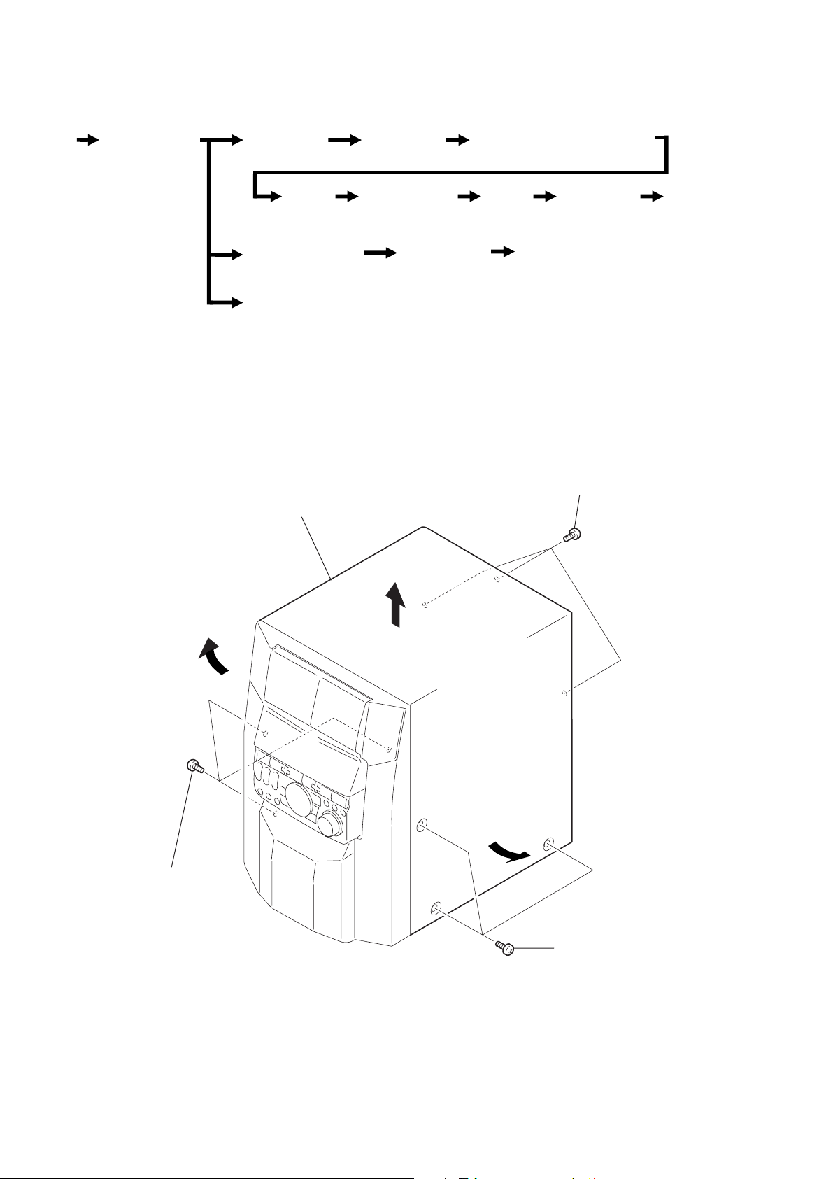
• This set can be disassembled in the order shown below.
SECTION 2
DISASSEMBLY
CASE
(Page 8)
Note: Follow the disassembly procedure in the numerical order given.
FRONT PANEL
SECTION
(Page 9)
BACK PANEL
(Page 10)
SUB
CHASSIS
(Page 11)
TAPE MECHANISM
DECK SECTION
(Page 14)
DOOR ASS’Y
(Page 9)
MAIN BOARD
(Page 10)
CD MECHANISM
DECK SECTION
(Page 12)
2-1. CASE
3
Case
POWER TRANSFORMER (T901)
(Page 11)
AUDIO BOARD
(Page 14)
BASE
UNIT
(Page 12)
BD BOARD,
SLED MOTOR
(M102)
(Page 13)
CAPSTAN MOTOR (M1)
(Page 15)
2
Three screws
(BVTP 3
OPTICAL
PICK-UP
(KSS-213D/Q-NP)
(Page 13)
×
8)
1
Three screws
(CASE3 TP2)
— 8 —
1
Three screws
(CASE3 TP2)
Page 9

2-2. FRONT PANEL SECTION
y
1
Wire (flat type)
(15 core)
8
Two claws
2
Wire (flat type)
(17 core)
5
Screws
(BVTT 3
6
Lug
×
8)
2-3. DOOR ASSY
1
Two screws
(PTPWH 2.6
4
Connector
3
Wire (flat type) (15 core)
8
Two claws
7
Three screws
(BVTP 3
×
8)
×
8)
2
Open the door ass'y
— 9 —
A
3
Remove the door ass'
to direction of the
arrow
A
.
Page 10

2-4. BACK PANEL
N
1
Wire (flat type) (13 core)
2
Connector
5
Thirteen screws
(BVTP 3
6
Remove the back panel
to direction of the arrow.
×
8)
4
Cover
3
Five screws
(BVTP 3
×
8)
2-5. MAIN BOARD
5
Two connectors
3
Four connectors
4
Three connectors
7
Remove the MAI
board to direction
of the arrow.
1
Wire (flat type) (16 core)
— 10 —
2
Wire (flat type) (9 core)
6
Two screws
(BVTP 3
×
8)
Page 11

2-6. POWER TRANSFORMER (T901)
d
)
4
Power transforme
3
Four screws
(BVTT 3
1
×
8)
Connector
2
Power cor
2-7. SUB CHASSIS
2
Three screws
(BVTP 3
1
(BVTT 3
3
Sub chassis
×
8)
Two screws
×
8)
— 11 —
2
Two screws
(BVTP 3
×
8
Page 12

2-8. CD MECHANISM DECK SECTION
)
5
Two screws
7
Reinforcement
1
Screw
(PTPWH 2.6
(BVTT 3
×
8)
×
6)
0
(BVTP 3
Screw
6
×
14)
Wire holder
8
Three screws
(BVTT 3
9
!¡
Screw
(BVTT 3
×
10)
Base (LOADING)
!™
×
10)
3
Bwo screws
(BVTP 3
Base (CDM
×
8)
2
Table (SO)
2-9. BASE UNIT
2
Bracket
1
Two screws
(BTVP 3
3
×
8)
Two tention springs
5
Base unit
4
Cover (CD)
4
Four screws
(PTPWH 2.6
×
8)
— 12 —
Page 13

2-10. BD BOARD, SLED MOTOR (M102)
)
6
Gear (A) (S)
5
Claw
!º
Two screws (+P 2 × 2)
!¡
Sled motor
(M102)
8
Gear cover
7
Three claws
9
Gear (B) (RP)
1
Wire (flat type) (16 core
4
BD board
3
four solders.
2-11. OPTICAL PICK-UP (KSS-213D/Q-NP)
3
Remove the optical
pick-up to direction
of the arrow
Removal
A
2
Screw (+PTPWH 2 × 5)
.
A
2
Sled shaft
1
Claw
— 13 —
Page 14

2-12. TAPE MECHANISM DECK SECTION
2
Remove the cassette lid (L) ass'y
to direction of the arrow
B
1
Remove the cassette lid (R) ass'y
to direction of the arrow
B
.
A
A
.
4
Remove the tape mechanism
deck section.
3
Three screws
(BVTP 2.6
3
Three screws
(BVTP 3
×
8)
×
6)
2-13. AUDIO BOARD
3
Two screws
(BTP 2.6
4
AUDIO board
×
4)
2
Break the soldering of two
flexible flat cables.
1
Four rivets
— 14 —
Page 15

2-14. CAPSTAN MOTOR (M1)
4
Removal the capstan motor
to direction of the arrow.
2
Hang the belt.
3
Hang the belt.
1
Two screws
(BTP 2.6
×
8)
— 15 —
Page 16

SECTION 3
TEST MODE
[MC Cold Reset]
* The cold reset clears all data including preset data stored in the
RAM to initial conditions. Execute this mode when returning
the set to the customer.
Procedure:
1. Press the three buttons STOP , ENTER and FUNCTION at
the same time.
2. The fluorescent indicator tube turns off for a moment and the
RAM is reset to the initial conditions.
[MC Hot Reset]
* This mode resets the set with the preset data kept stored in the
memory. This hot reset mode is performed also when the power
cord is plugged in and out.
Procedure:
1. Press the three buttons STOP , ENTER and GROUP 1 at the
same time.
2. The fluorescent indicator tube turns off for a moment and the
RAM is reset to the initial conditions.
[CD Initial]
* The CD INITIAL clears all of the CD related data. Execute
this mode when returning the set to the customer.
Procedure:
1. Press the three buttons STOP , ENTER and GROUP 4 at the
same time.
2. The message “ALL ERASE” appears on the fluorescent
indicator tube and the CD related data is reset to the initial
conditions.
[CD Line Test]
* The CD Line test displays the rotating time required for one
rotation by rotating the disc tray.
Procedure:
1. Press the three buttons STOP , ENTER and GROUP 5 at the
same time. The CD PLA Y LED and the CD PAUSE LED flash
alternately and the disc tray starts rotation.
2. The message “xx << y.y” appears on the fluorescent indicator
tube. The left numbers count up the discs starting from 1 to 51.
The left numbers “y.y” indicate the rotating time required for
one rotation by rotating the disc tray.
3. To exit the CD LINE test mode, execute the MC Hot Reset.
[CD Memo All Clear]
* The mode clears all contents of the CD disc memo. Execute
this mode when returning the set to the customer.
Procedure:
1. Press the two buttons MEMO INPUT and FLASH at the
same time.
2. The message “ALL ERASE” appears on the fluorescent
indicator tube and the CD disc memo is all cleared.
[GC Test Mode]
* This mode checks microprocessor version number, keys,
fluorescent tubes, LEDs and VACS (Variable Attenuation
Control System).
Procedure:
1. Press the three buttons STOP , ENTER and GROUP 2 at the
same time. The HCD-F250 enters the GC test mode, and all of
the fluorescent tubes and LEDs turn on.
2. From this state, any one of the three modes GROUP 1, GROUP
2 and GROUP 3 can be selected. Go to step 3 to enter the
GROUP 1 test mode. Go to step 5 to enter the GROUP 2 test
mode. Go to step 11 to enter the GROUP 3 test mode.
3. [GROUP 1 test mode ] From the state of step 2, press the
GROUP 1 button. Every pressing of the GROUP 1 button
advances the following check modes and displays in the given
order. Model name display, destination display, MC version
display, GC version display, DC version display, VC version
display and CC version display.
4. To exit the GC test mode and to return to the STANDBY mode,
press the STOP , ENTER and GROUP 2 buttons again.
5. [GROUP 2 test mode ] You can enter this mode directly from
step 2. When you performed steps 3, perform steps 4, then 1
and 2 before starting the step 5.
[GROUP 2 test mode ] From the GC test mode, press the
GROUP 2 button to enter the key check mode. The display: K
1, J 0, V 0 appears.
6. The value after K indicates the number of times that the key is
pressed. 1 is displayed because the GROUP 2 button has
already been pressed.
7. When other keys are pressed one after another, the key count
increases up to 42. The keys which have already been pressed,
are not counted.
8. The value after J indicates the number of clicks that the JOG
dial is rotated. The clockwise rotation increases the count value.
The counter-clockwise rotation decreases the count value.
9. The value after V also indicates amount of rotation of volume
control. The clockwise rotation increases the count value. The
counter-clockwise rotation decreases the count value.
10. To exit the GC test mode and to return to the STANDBY mode,
press the STOP , ENTER and GROUP 2 buttons again.
11. [GROUP 2 test mode ] You can enter this mode directly from
step 2. When you performed steps 3, perform steps 4, then 1
and 2 before starting the step 5.
[GROUP 3 test mode ] From the GC test mode, press the
GROUP 3 button to enter the VACS attenuation check mode.
The display: VOL NORMAL appears.
12. To exit the GC test mode and to return to the STANDBY mode,
press the STOP , ENTER and GROUP 2 buttons again.
[MC Test Mode]
* This mode checks operation of amplifier and cassette deck.
How to enter the MC test mode:
Press the three buttons of STOP , ENTER and GROUP 3 . “EQ
CHECK” display on the FL tube and the VOLUME display flash.
In addition the LEDs of the JOG dial, FF and REW flash indicating
the MC test mode.
Check procedure:
You can perform any of the following five steps. However, it is
recommended to perform them in the following order because the
skipped cannot be performed if the checks are not performed in the
given order.
1. EQ Check Mode
The GEQ becomes maximum when the JOG dial is turned
clockwise.
The GEQ becomes minimum when the JOG dial is turned
counter-clockwise.
The GEQ comes to center when the FILE SELECT button is
pressed.
— 16 —
Page 17

2. VOLUME Check Mode
The maximum volume is set, and the VOLUME MAX display
and the GEQ display are displayed for a moment regardless of
the amount of volume rotation.
The minimum volume is set, and the VOLUME MIN display
and the GEQ display are displayed for a moment regardless of
the amount of volume rotation.
3. Deck Check Mode
Install a tape to the deck B. Select T APE B with the FUNCTION
button.
Recording starts and PAUSE is released when the REC button
is pressed.
VIDEO is selected by the input FUNCTION.
Press the STOP button to stop recording and select TAPE B
with the FUNCTION button.
Rewind the tape by pressing the REW button and stop at the
recording start point. Start playback from the recording start
point.
4. High Speed Check Mode-1
Install a tape to the deck A. Select T APE A with the FUNCTION
button.
Press the PLAY button then press the HI-SPEED DUBBING
button during playback.
The normal playback is obtained during normal speed playback
and the double speed playback is obtained during the double
speed playback.
5. High Speed Check Mode-2
Install a tape to the deck B. Select T APE B with the FUNCTION
button.
Press the REC button. When the P AUSE is released , recording
is started.
When the HI-SPEED DUBBING button is pressed during
recording, the double speed recording is established only when
the button is pressed.
[Aging Mode]
The decks A and B are operated automatically for aging purpose.
When errors occur during aging, causes of errors are displayed and
the aging mode is stopped.
5. The tape A is rewound and stops at the shut-off. The aging
mode advances to the next step.
The message: TAPE A AG-5 appears.
6. The tape B is played back in the FWD mode. After two minutes
of the FWD playback, the aging mode advances to the next
step.
The message: TAPE B AG-2 appears.
7. The tape B runs in fast forward. After two minutes of fast
forward, or at the shut-off point, the tape is stopped and the
aging mode advances to the next step.
The message: TAPE B AG-3 appears.
8. The tape B is played back in the R VS mode. After two minutes
of the RVS playback, the aging mode advances to the next step.
The message: TAPE B AG-4 appears.
9. The tape B is rewound and stops at the shut-off. The aging
mode advances to the next step.
The message: TAPE B AG-5 appears.
[Function Change Mode]
* Select either VIDEO or MD of the external FUNCTION input.
Procedure:
1. Turn off the power.
2. Press the two buttons ENTER and POWER at the same time.
The main power is turned on and the other function of the
previous function is selected and displayed. “MD” or “VIDEO”
[AM TUNER STEP 9 kHz/10 kHz Selection Mode]
* Either the 9 kHz step or 10 kHz step can be selected for the AM
channel step.
Procedure:
1. Turn on the power and select TUNER using the FUNCTION
button.
2. Select AM with the TUNER/BAND button and turn off the
power.
3. Press the two buttons ENTER and POWER at the same time.
The main power is turned on and the other frequency step of
the previous mode is selected and displayed. “AM 9k STEP”
or “AM 10k STEP”
How to enter the aging mode
1. Turn on the main power. Install a playback tape to deck A and
install a blank tape to deck B.
2. Select TAPE A with the FUNCTION button.
3. Press the three buttons of STOP , ENTER and GROUP
ENTRY at the same time to enter the aging mode.
How to exit the aging mode.
Turn off the main power.
1. Rewind the tapes A and B. Tapes stop at the shut-off of tape A
and the aging mode advances to the next step.
The message: TAPE A AG-1 appears.
2. The tape A is played back in the FWD mode. After two minutes
of the FWD playback, the aging mode advances to the next
step.
The message: TAPE A AG-2 appears.
3. The tape A runs in fast forward. After two minutes of fast
forward, or at the shut-off point, the tape is stopped and the
aging mode advances to the next step.
The message: TAPE A AG-3 appears.
4. The tape A is played back in the RVS mode. After two minutes
of the RVS playback, the aging mode advances to the next step.
The message: TAPE A AG-4 appears.
— 17 —
Page 18

SECTION 4
e
MECHANICAL ADJUSTMENT
• TAPE MECHANISM DECK SECTION
Precaution
• Tor que Measurement
Mode
1. Clean the following parts with a denatured alcohol-moistened
swab:
record/playback heads pinch rollers
erase head rubber belts
capstan idlers
2. Demagnetize the record/playback head with a head
demagnetizer.
3. Do not use a magnetized screwdriver for the adjustments.
4. After the adjustments, apply suitable locking compound to the
parts adjusted.
5. The adjustments should be performed with the rated power
supply voltage unless otherwise noted.
FWD
FWD
back tension
REV
REV
back tension
FF/REW
FWD tension
REV tension
• CD MECHANISM DECK SECTION
To adjust the mechanism section, enter the mechanism section adjustment mode.
For how to enter the mechanism section adjustment mode, refer to each adjustment section.
Torque meter
CQ-102C
CQ-102C
CQ-102RC
CQ-102RC
CQ-201B
CQ-403A
CQ-403R
Meter reading
31 to 71 g • cm
(0.43 – 0.98 oz • inch)
2 to 6 g • cm
(0.02 – 0.08 oz • inch)
31 to 71 g • cm
(0.43 – 0.98 oz • inch)
2 to 6 g • cm
(0.02 – 0.08 oz • inch)
71 to 143 g • cm
(0.98 – 1.99 oz • inch)
100 g or more
(3.53 oz or more)
100 g or more
(3.53 oz or more)
DISC SENSOR ALIGMENT
1. Make sure that there is no disc in the unit.
2. Connect an oscilloscope to IC401$™, IC4024 of the MAIN board.
oscilloscop
IC401$™ D.SENS (CH1)
IC401
4
HHOUT (CH2)
GND
3. Turn the power switch on.
4. Press the p button, ENTER button and GROUP 5 button simultaneously.
— 18 —
Page 19
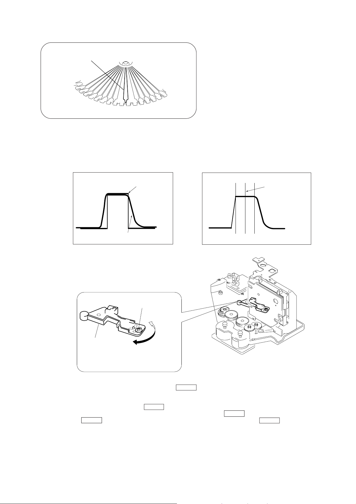
PLUS ONE
5. The disc table rotates in the clockwise direction. The disc table rotation time is displayed with ‘’PLUS ONE” slit as a measuring point.
6. Measure the waveform of the oscilloscope when the disc table is rotating.
7. Move the holder (sensor) center so that the flat portion center at the top of the D.SENS (CH1) input waveform and the ‘’H” center of
HHOUT (CH2) coincide.
D.SENS (CH1) waveform
Holder (sensor)
HHOUT (CH2) waveform
Fixed screw
Flat portion center of
D.SENS (CH1) waveform
8. Tighten the fixed screw to fix the disc table, then press the CLEAR button.
9. The disc table rotates in the counterclockwise direction. Measure the waveform and make sure that the flat portion center at the top of the
D.SENS (CH1) input waveform and the ‘’H” center of HHOUT (CH2) coincide.
10. If the adjustment is not successful, press the CLEAR button to rotate the disc table in the clockwise direction, and perform steps 6 to 9.
Note: During the adjustment mode, the rotational direction is switched each time the CLEAR button is pressed.
Pressing the CHECK button enters the loading mode which will be described later. Pressing the CLEAR button rotates the disc table
again.
— 19 —
Page 20
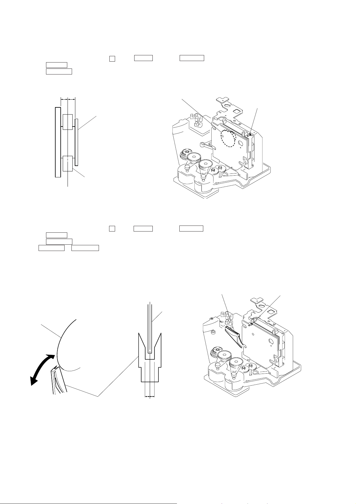
MAGNET ASSY ALIGMENT
)
1. Check that there is no disc in the unit and then turn ON the power. Open the door, and set a disc in the PLUS ONE slit.
2. Close the door, and while pressing the
3. Press the CHECK button, and set the loading mode.
4. Press the + ‚± button and chuck the disc.
5. Adjust the magnet assembly and magnet holder so that A=B as shown in the figure.
p button, ENTER button and GROUP 5 button simultaneously.
AB
Magnet ASSY
Magnet holder
Magnet ASSY
Screw (For adjustment
DISC HOLDER A ALIGMENT
1. Check that there is no disc in the unit and then turn ON the power. Open the door, and set a disc in the PLUS ONE slit.
2. Close the door, and while pressing the
3. Press the CHECK button, and set the loading mode.
4. Press the + ‚± button and chuck the disc.
5. Press + ‚± or ≠º – button to stop the disc holder A slightly away from the disc.
6. Rotate and adjust the adjusting screw so that the center of the disc and that of the disc holder coincide.
p button, ENTER button and GROUP 5 button simultaneously.
Disc
Disc holder A
a
a = b
Disc holder A
Disc
b
Screw (For adjustment)
— 20 —
Page 21

SECTION 5
ELECTRICAL ADJUSTMENTS
DECK SECTION
0 dB=0.775 V
1. Demagnetize the record/playback head with a head
demagnetizer.
2. Do not use a magnetized screwdriver for the adjustments.
3. After the adjustments, apply suitable locking compound to the
parts adjust.
4. The adjustments should be performed with the rated power
supply voltage unless otherwise noted.
5. The adjustments should be performed in the order given in this
service manual. (As a general rule, playback circuit adjustment
should be completed before performing recording circuit
adjustment.)
6. The adjustments should be performed for both L-CH and RCH.
7. Switches and controls should be set as follows unless otherwise
specified.
• Test Tape
Tape Signal Used for
P-4-A100 10 kHz, –10 dB Azimuth Adjustment
WS-48B 3 kHz, 0 dB Tape Speed Adjustment
P-4-L300 315 Hz, 0 dB Level Adjustment
Record/Playback Head Azimuth Adjustment
DECK A DECK B
Note: Perform this adjustments for both decks
Procedure:
1. Mode: Playback
test tape
P-4-A100
(10 kHz, –10 dB)
set
main board
CN301
Pin
3
(L-CH)
Pin
1
(R-CH)
main board
CN301
Pin
2
(GND)
level meter
+
–
2. Turn the adjustment screw and check output peaks. If the peaks
do not match for L-CH and R-CH, turn the adjustment screw
so that outputs match within 1dB of peak.
Output
level
within
1dB
L-CH
peak
R-CH
peak
within
1dB
Screw
position
L-CH
peak
Screw
position
R-CH
peak
3. Mode: Playback
test tape
P-4-A100
(10 kHz, –10 dB)
L-CH
MAIN
board
CN301
set
R-CH
waveform of oscilloscope
in phase 45°90°135°180
pin
L
R
pin
good
3
pin
1
2
oscilloscope
V
wrong
H
°
4. After the adjustments, apply suitable locking compound to the
pats adjusted.
Adjustment Location:Playback Head (Deck A).
Record/Playback/Erase Head (Deck B).
— 21 —
Page 22

Tape Speed Adjustment
r
Note: Start the Tape Speed adjustment as below after setting to the test
mode.
In the test mode, the tape speed is high during pressing the
HI-SPEED DUBBING button.
DECK B
Procedure:
1. Turn the power switch on.
2. Press the
p button, ENTER button and GROUP 3 button
simultaneously.
(The “VOLUME” on the fluorescent indicator tube will blink
while in the test mode.)
To exit from the test mode, press the
I/u button.
Mode: Playback
test tape
WS-48B
(3 kHz, 0 dB)
set
main board
CN301 (Pin
frequency counter
3
: L-CH)
(Pin
1
: R-CH)
+
–
1. Insert the WS-48B into the deck B.
2. Press the · button on the deck B.
3. Press the HI-SPEED DUBBING button in playback mode.
Then at HIGH speed mode.
4. Adjust RV1001 on the LEAF SW board do that frequency
counter reads 6,000 ± 180 Hz.
5. Press the HI-SPEED DUBBING button.
Then back to NORMAL speed mode.
6. Adjust RV1002 on the LEAF SW board so that frequency
counter reads 3,000 ± 90 Hz.
Adjustment Location: LEAF SW board
REC Bias Adjustment DECK B
Procedure:
INTRODUCTION
When set to the test mode performed in Tape Speed Adjustment,
when the tape is rewound after recording, the “REC memory mode”
which rewinds only the recorded portion and playback is set.
This “REC memory mode” is convenient for performing this
adjustment. During recording, the input signal FUNCTION will
automatically switch to VIDEO.
(If do not operation of stopped from recording complete, after
selecting DECK B with the FUNCTION button, and press
≠º – button then rewind to recording start position.)
1. Press [FUNCTION] button to select VIDEO. (This step is not
necessary if the above test mode has already been set.)
2. Insert a tape into deck B.
3. After press [ REC] button, press P button, then recording
r
start.
4. Mode: Record
MD/VIDEO (AUDIO) IN
1) 315 Hz
2) 10 kHz
AF OSC
attenuator
50 mV (–23.8 dB)
600
Ω
set
blank tape
CN-123
5. Mode: Playback
recorded
portion
level mete
Sample Value of Wow and filter
W,RMS (JIS) within 0.3%
(test tape: WS-48B)
Playback level Adjustment
DECK A DECK B
Procedure:
Mode: Playback
test tape
P-4-L300
(315 Hz, 0 dB)
set
main board
CN301 (Pin
(Pin
level meter
3
: L-CH)
1
: R-CH)
+
–
Deck A is RV311 (L-CH) and RV411 (R-CH), Deck B is RV301
(L-CH) and RV401 (R-CH) so that adjustment within adjustment
level as follows.
Adjustment Level:
CN301 PB level: 301.5 to 338.3 mV (–8.2 to –7.2 dB) level
difference between the channels: within ±0.5 dB
Adjustment Location: AUDIO board
3
1
+
–
: L-CH)
: R-CH)
set
CN301 (Pin
(Pin
6. Confirm playback the signal recorded in step 3 become
adjustable level as follows.
If these levels do not adjustable level, adjustment the RV341
(L-CH) and RV441 (R-CH) on the AUDIO board to repeat steps
4 and 5.
Adjustable level: Playback output of 315 Hz to playback
output of 10 kHz: ±1.0 dB
Adjustment Location: AUDIO board
REC Level Adjustment
DECK B
Procedure:
INTRODUCTION
When set to the test mode performed in Tape Speed Adjustment,
when the tape is rewound after recording, the “REC memory mode”
which rewinds only the recorded portion and playback is set.
This “REC memory mode” is convenient for performing this
adjustment. During recording, the input signal FUNCTION will
automatically switch to VIDEO.
(If do not operation of stopped from recording complete, after
selecting DECK B with the FUNCTION button, and press
≠º – button then rewind to recording start position.)
1. Press
[FUNCTION] button to select VIDEO. (This step is not
necessary if the above test mode has already been set.)
2. Insert a tape into deck B.
3. After press
[REC] button, press P button, then recording
r
start.
— 22 —
Page 23
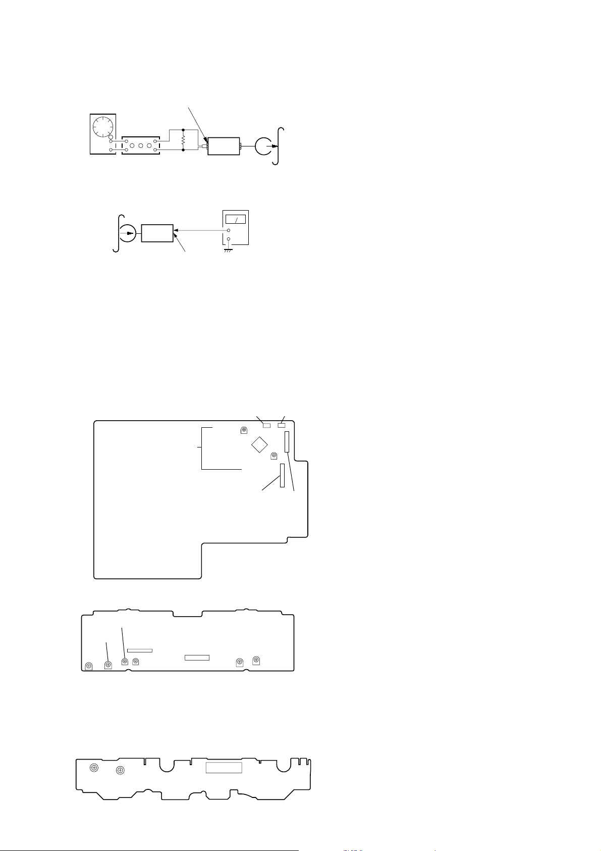
4. Mode: Record
r
MD/VIDEO (AUDIO) IN
AF OSC
315 Hz, 50 mV (–23.8 dB)
attenuator
5. Mode: Playback
recorded
portion
600
Ω
blank tape
CS-123
set
level mete
3
1
+
–
: L-CH)
: R-CH)
set
CN301 (Pin
(Pin
6. Confirm playback the signal recorded in step 3 become
adjustable level as follows.
If these levels do not adjustable level, adjustment the RV301
(L-CH) and RV351 (R-CH) on the MAIN board to repeat steps
4 and 5.
Adjustable level:
CN301 PB level: 47.2 to 53.0 mV (–24.3 to –23.3 dB)
Adjustment Location: MAIN board
[MAIN BOARD] (Component Side)
CN302
CN301
RV301
L
REC LEVEL
IC301
RV351
R
CN107
CN106
[AUDIO BOARD] (Component Side)
RV441
RV401
RV301
LR
PB LEVEL
– DECK B –
[LEAF SW BOARD] (Component Side)
TAPE SPEED
(NORMAL) (HIGH)
RV1002
RV1001
IC602
RV341
RL
REC BIAS
CN601
RV311
PB LEVEL
– DECK A –
CN1001
RV411
LR
— 23 —
Page 24

CD SECTION
Note :
1. CD Block is basically designed to operate without adjustment.
Therefore, check each item in order given.
2. Use YEDS-18 disc (3-702-101-01) unless otherwise indicated.
3. Use an oscilloscope with more than 10MΩ impedance.
4. Clean the object lens by an applicator with neutral detergent
when the signal level is low than specified value with the
following checks.
oscilloscope
BD board
TP (FE)
TP (VC)
S Curve Check
Procedure :
1. Press the 1/u button to turn ON the power .
2. Open the front cover, and press the CD PLUS ONE button.
3. Set the disc (YEDS-18) into the “PLUS ONE” slit.
4. Close the front cover, and chuck the disc.
5. Press the 1/u button to turn OFF the power.
6. Connect the oscilloscope to TP (FE) of the BD board.
7. Connect TP (ADJ) of the MAIN board and connect TP (GND)
with a lead wire.
8. Press the 1/u button to turn ON the power.
9. The first track will be played back automatically. When the
CHECK button is pressed, “S JI” will be displayed on the
fluorescent indicator tube, and focus search will be repeated.
10. Check the oscilloscope waveform (S-curve) is symmetrical
between A and B. And confirm peak to peak level within 1.8 ±
0.6 Vp-p.
S-curve waveform
symmetry
A
within 1.8 ± 0.6Vp-p
B
11. Turn OFF the power, and remove the lead wire connected at
step 7.
Note : • Try to measure several times to make sure than the ratio
of A : B or B : A is more than 10 : 7.
• Take sweep time as long as possible and light up the
brightness to obtain best waveform.
RF Level Check
oscilloscope
BD board
10. Confirm that oscilloscope waveform is clear and check RF signal
level is correct or not.
11. Turn OFF the power, and remove the lead wire connected at
step 7.
Note : A clear RF signal waveform means that the shape “◊” can be
clearly distinguished at the center of the waveform.
RF signal waveform
VOLT/DIV : 200mV
TIME/DIV : 500ns
level : 1.8 ± Vp-p
+0.3
–0.2
E-F Balance (Traverse) Check
The procedure for this checking method differs for when a general
remote control unit is used and not used.
oscilloscope
BD board
TP (TE)
TP (VC)
When a general remote commander is used:
1. Press the 1/u button to turn ON the power.
2. Open the front cover, and press the CD PLUS ONE button.
3. Set the disc (YEDS-18) into the “PLUS ONE” slit.
4. Close the front cover, and chuck the disc.
5. Press the 1/u button to turn OFF the power.
6. Connect the oscilloscope to TP (TE) of the BD board.
7. Connect TP (ADJ) of the MAIN board and connect TP (GND)
with a lead wire.
8. Press the 1/u button to turn ON the power.
9. Playback the fifth track of the disc.
10. Press the 3 button on the remote commander. (The tracking
servo and the sledding servo are turned OFF.)
11. Check the level B of the oscilliscope's waveform and the A (DC
voltage) of the center of the Traverse waveform.
Confirm the following :
A/B x 100 = less than ± 10%
Traverse waveform
0V
Center of the waveform
B
A (DC voltage)
level : 0.7 ± 0.3 Vp-p
TP (RF)
TP (VC)
Procedure :
1. Press the 1/u button to turn ON the power.
2. Open the front cover, and press the CD PLUS ONE button.
3. Set the disc (YEDS-18) into the “PLUS ONE” slit.
4. Close the front cover, and chuck the disc.
5. Press the 1/u button to turn OFF the power.
6. Connect the oscilloscope to TP (RF) of the BD board.
7. Connect TP (ADJ) of the MAIN board and connect TP (GND)
with a lead wire.
8. Press the 1/u button to turn ON the power.
9. Playback the fifth track of the disc.
— 24 —
12. Press the 8 button on the remote control unit. (The tracking ser vo and
sledding servo are turned ON.) Confirm the C (DC voltage) is almost equal
to the A (DC voltage) is step 11.
Traverse waveform
0V
Tracking servo
Sled servo
OFF
Tracking servo
Sled servo
ON
C (DC
voltage)
13. Turn OFF the power, and remove the lead wire connected at
step 7.
Page 25

oscilloscope
BD board
TP (TE)
TP (VC)
When a general remote commander is not used:
1. Solder lead wires to TP (DVDD) and TP (TOFF) on the BD
board severally.
2. Connect the oscilloscope to TP (TE) of the BD board .
3. Press the POWER button to turn ON the power.
4. Open the front cover, and press the CD PLUS ONE button.
5. Set the disc (YEDS-18) into the “PLUS ONE” slit.
6. Close the front cover, and chuck the disc.
7. Playback the fifth track of the disc.
8. Short-circuit the lead wire connected at step 1. (The tracking
servo is turned OFF)
9. Check the level B of the oscilliscope's waveform and the A
(DC voltage) of the center of the Traverse waveform.
Confirm the following :
A/B x 100 = less than ± 10%
Traverse waveform
0V
Center of the waveform
B
A (DC voltage)
About RV402 on the MAIN board
RV402 of the MAIN board r equires no adjustments. Please note
that it should be dixed to mechanical center position when you
moved and do not know origin position.
Adjustment Location :
[ BD BOARD ] — CONDUCTOR SIDE —
CN102
TP
(VC)
TP
(RF)
IC102
TP
(TOFF)
IC101
TP
(TE)
TP
(PLCK)
TP
(DVDD)
TP
(FE)
CN103
CN101
level : 0.7 ± 0.3 Vp-p
10. Disconnect the lead wire short-circuited at step 8. (The tracking
servo is turned ON.) Confirm the C (DC voltage) is almost equal
to the A (DC v oltage) is step 8.
Traverse waveform
C (DC
0V
Tracking servo
OFF
Tracking servo
ON
voltage)
11. Turn OFF the power, and remove the lead wire connected at
step 1.
RF PLL Free-run Frequency Check
Procedure :
1. Connect the frequenc y counter to TP (PLCK) of the BD board.
BD board
TP (PLCK)
frequency counter
[ MAIN BOARD ] — COMPONENT SIDE —
CN301
RV301
IC301
RV351
CN107
CN302
CN106
2. Press the POWER button to turn ON the power.
3. Open the front cover, and press the CD PLUS ONE button.
4. Set the disc (YEDS-18) into the “PLUS ONE” slit.
5. Close the front cover, and chuck the disc.
6. Playback the fifth track of the disc.
7. Confirm that reading on frequency counter is 4.3218 MHz ±
30 kHz.
— 25 —
Page 26
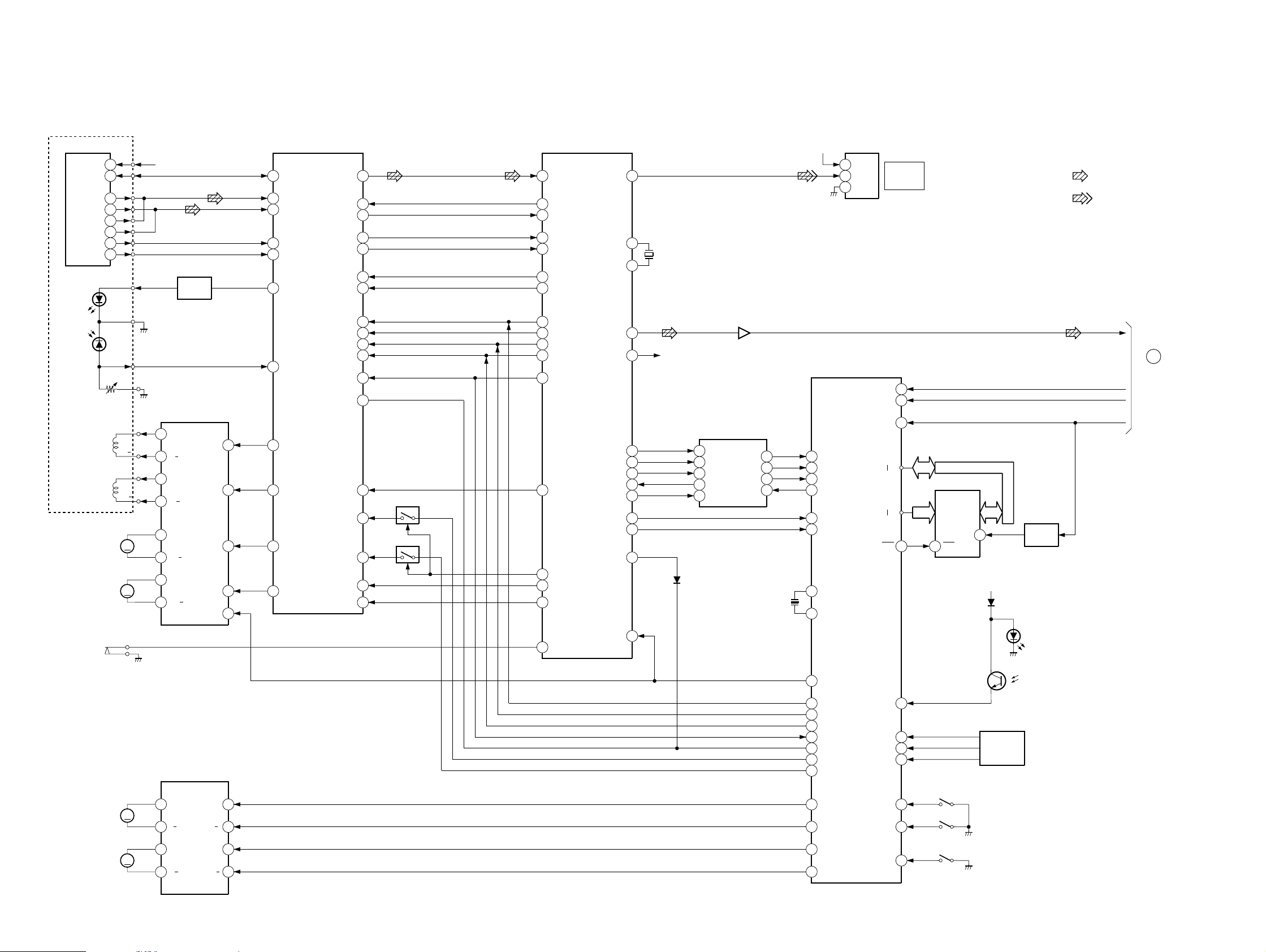
HCD-F150/FR10
6-1. BLOCK DIAGRAM — CD SECTION —
OPTICAL PICK-UP
BLOCK
(KSS -213 B/S-N)
DETECTOR
VCC
VC
7
8
A
4
B
2
C
1
D
5
E
6
F
10
LD
A+5V
Q103
LD
DRIVER
SECTION 6
DIAGRAMS
FOCUS/TRACKING/
SLED/SPINDLE SERVO
RF AMP
IC101
58
VR
2
FIN 1
1
FIN 2
3
E
4
F
62
LDD
RF SM
TES
HFL
DIGITAL SIGNAL
PROCESSOR
IC102
41
44SLI
49DEF
36
37
33JP+
32JP-
10
EFMI
9
EFMO
1
DEF
16
TES
15
HFL
19
JP+
20
JP-
D OUT
XO
31
XI
45
44
X101
16.9344M
A+5V
IC402
VDD
D IN
GND
CD
DIGITAL
OUT
• SIGNAL PATH
:CD
:DIGITAL OUT
FOCUS
COIL
TRACKING
COIL
M102
SLED
MOTOR
M101
SPINDOL
MOTOR
S101
LIMIT
VR
GND
PD
2
4
5
1
3
FILTER AMP
CD TEXT
DECODER
IC104
SBSO
WFCK
MCK
FXCK
SCOR
IC441
SRDT
SCLK
CD L
CD CHANGER
CONTROL
IC401
IIC DATA
12
11
13DQSY
6XMODE
X401
66
65
64
67
55
49
32
31
SRDT
SCLK
DQSY
XMODE
WRQ
SQOUT
XTAL
EXTAL
IIC CLK
RESET
D0
D7
A0
A14
WE
80
78
30
8
SRAM
IC411
27
29
WE
CE
20
815
U+5V
D402
Q411
RESET
SW
D51
D51
DISC
SENSOR(S)
IIC DATA
IIC CLK
RESET
B
TO/FROM
MAIN
BLOCK
(Page 29)
52DATA
CLK
50
CL
51
CE
TGL
DRF
SL+
SL-
CV-
53
34
54
35TOFF
Q102
31
Q101
30
40CV+
39
63
LDS
FCS/TRK COIL
SL/SP MOTOR
DRIVER
IC103
F+
18
F+
F
17
F
T+
19
T+
T
20
T
8
SL+
M
7
SL
6
SP+
M
SP
5
F IN
T IN
SL IN
SP IN
MUTE
15
22
10
3
2
16
FD
15
TO
29
SLD
27
SPD
56
61
57
54
18
17
26
12
13
27
COIN
4.2M
CQCK
RWC
TGL
TOFF
CONT3
CLV+
CLV-
CONT4
L CH
R CH
PW
SFSY
16M
CBCK
SBSY
WRQ
SQOUT
RD
RESET
37
40
49
50
60
51
47
53
55
3
58
R CH
D151
M61
LOADING
MOTOR
M62
TABLE
MOTOR
2
DB RESET
50
COIN
48
CQCK
58
RWC
MOTOR DRIVER
IC461
8
L+
57
TGL
54
DRF
47
SL+
59
SL-
L+
3
76
LD OUT
TSENS 1
TSENS 2
TSENS 3
M
9
L
11
T+
L
2
T+
16
M
T
10
16
T
17
77
LD IN
75
TBL L
74
TBL R
DOWN SW
DOOR SW
UP SW
42D SENS
62
61
63
70
71
69
TABL
SENSOR
IC51-53
S51
(UP)
S52
(DOWN)
S413
(DOOR)
Q51
DISC
SENSOR
— 27 — — 28 —
Page 27
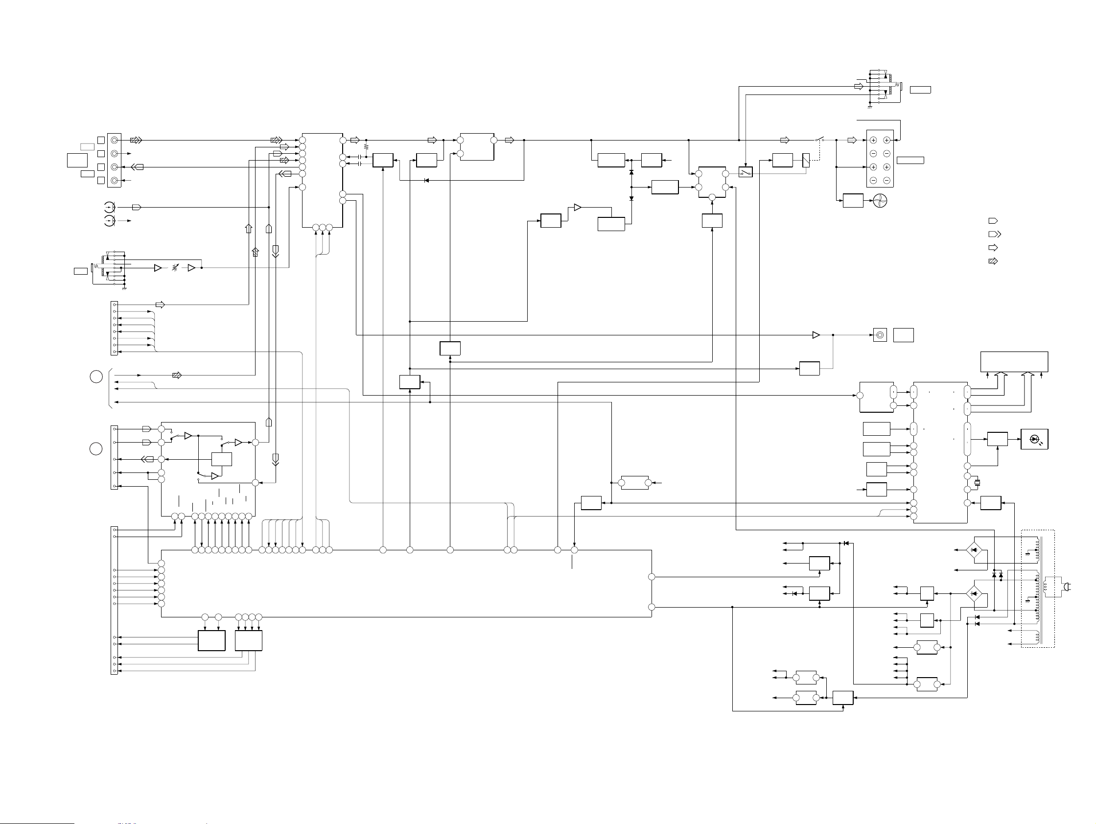
6-2. BLOCK DIAGRAM — MAIN SECTION —
HCD-F150/FR10
VIDEO/
MD
J782
J782
MIC
IN
OUT
PB
TO/FROM
TUNER
UNIT
TO/FROM
CD
BLOCK
(Page 28)
TO/FROM
AUDIO
BLOCK
(Page 32)
TO/FROM
BLOCK
R CH
Q703,704
VOLUME
P U+5V
D914
Q911-914
POWER
SWITCH
R CH
FAN
DRIVE
S651
TM701
LR
J191
SPEANA
4
IC603
S601-644
FUCTION
KEY
ROTARY
ENCODER
S652
JOG
SIRCS
IC402
A +7V
TC +7V
TC -7V
CD -UNREG
FAN M -UNREG
CD M+7V
P U+5V
CD U+5V
M U+5V
TC EMRG M+5V
IIC DATA
IIC CLK
A-7V
SOUND
J101
L
R
L
R
L
R
B
A
TC
16
CN102
CN106
CN107
ST L
ST D OUT
ST D IN
ST CLK
ST CE
TUNED
STEREO
ST MUTE
CD L
IIC DATA
IIC CLK
RESET
A PB L
B PB L
REC L
BIAS
RELAY
A 120/70
B 120/70
A PLAY
B PLAY
A HALF
B HALF
A SHUT
B SHUT
A TRG M+
B TRG M-
CAP M H/L
CAP M+
CAP M-
R CH
R CH
R CH
R CH
IC781 IC781
48
46
EQ
36
32
BIAS
33
BIAS
B NORM/CROM/METAL
A 120/70
19
17
97
TC RELAY
95
A PLAY
96
B PLAY
98
A HALF
28
B HALF
26
A SHUT
27
B SHUT
DOLBY PROLOGIC
MATRIX DECODER
IC301
DOLBY
B-NR
MS OUT
NROM/HIGH
REC/PB PASS
PB A/B
26
24
18
16
88
31
94
PB A/B
AMS IN93EQ H/N
R/P PASS
A TRG84B TRG
83
TRG
MOTOR
DRIVE
Q331-334
LN ON/OFF25NR ON/OFF23RN ON/OFF
BIAS ON/OFF
22
20
87
89
90
92
BIAS
TC MUTE
REC MUTE
NR ON/OFF
CAP H/L
82
85
CAP
MOTOR
DRIVE
Q335-343
40
43
ALC ON/OFF
15
ST MUTE
99
70
72
ST MUTE
ALC ON/OFF
CAPM CMT1M
CAP CTM2M86CAPM CNT1P
17
TUNED
STEREO
69
TUNED
STEREO
ST CE
68
CONTROL
IC101
69
IN A
66
IN B
67
IN C
68
IN D
57
REC B
58
REC A
2
MIC IN
ST CLK
ST D IN
ST D OUT
66
67
65
ST CE
ST CLK
ST D IN
ST D OUT
33
DATA
52
DATA
DATA
CLOCK
CLOCK
51
DATA
L OUT
BB A
BB B
KIY
VOL
CLOCK32LATCH
34
LATCH
LATCH
3
CLK
LATCH
36
39
38
60
40
Q111,112
DBFB
SWITCH
2
Q571,572
DBFB H/L
MUTE
CONT
1
Q113
MUTE
Q141
LINE MUTE
SYSTEM
CONTROL
IC501
Q575
MUTE
100
1
6
STK MUTE
POWER
AMP
IC801
10
Q801
OVER
LOAD DET
REAR AMP
IC831
Q292
MUTE
IIC CLK
IIC DATA
6
55
56
IIC CLK
IIC DATA
15
F RELAY
RESET
RESET
Q501
OVER
LOAD DET
Q831,834,881
D813
D863
RESET
3 1
IC502
CD POWER
POWER
Q811,812
HEAT
SENSOR
46
5
Q731
OVER
LOAD DET
M U D+5V
Q701,702
RDS D+5V
AUDIO D+5V
MUTE +5V
ST A+10V
PL VCC
TC M+12V
TC D+5V
CD A+5V
RELAY
DRIVE
+B
2 6
CONTROL
1
Q733
RELAY
IC701
7
MUTE
Q732
4
D917
MUTE
IC904
REG
IC903
REG
Q191
RY701
IC191
Q907,908
POWER
SWITCH
Q905,906
POWER
SWITCH
13
13
FAN
WOOFER
17
14
13
(FRONT)
SPEAKER
(REAR)
SUPER
J781
PHONS
DISPLAY CONTROL
IC601
34
SPEANA0
37
SPEANA3
32
L+R
26
KEY0
29
KEY3
19
VOL A
20
VOL B
21
JOG A
22
JOG B
33
SIRCS
10
RESET
24
DATA
23
CLOCK
MAIN +B
Q901,902,915
REG
Q916,951,952
REG
IC901
REG
IC902
REG
MAIN -B
13
13
SEG1
SEG20
G1
G13
LED1
LED16
LED SEL
D901-904
XO
XI
D821
D821
54
77
41
53
1
6
.
11
18
.
31
25
8
9
78VKK
• RCH is omitted
• Signal Path
: PB
: REC
: FM
: CD
FL601
DISPLAY
F1 F2
D611-628
D630-640
F1
F2
X601
Q910
-30V
REG
Q601-604
Q608-612
LED
DRIVER
T991
AC
IN
— 29 — — 30 —
Page 28
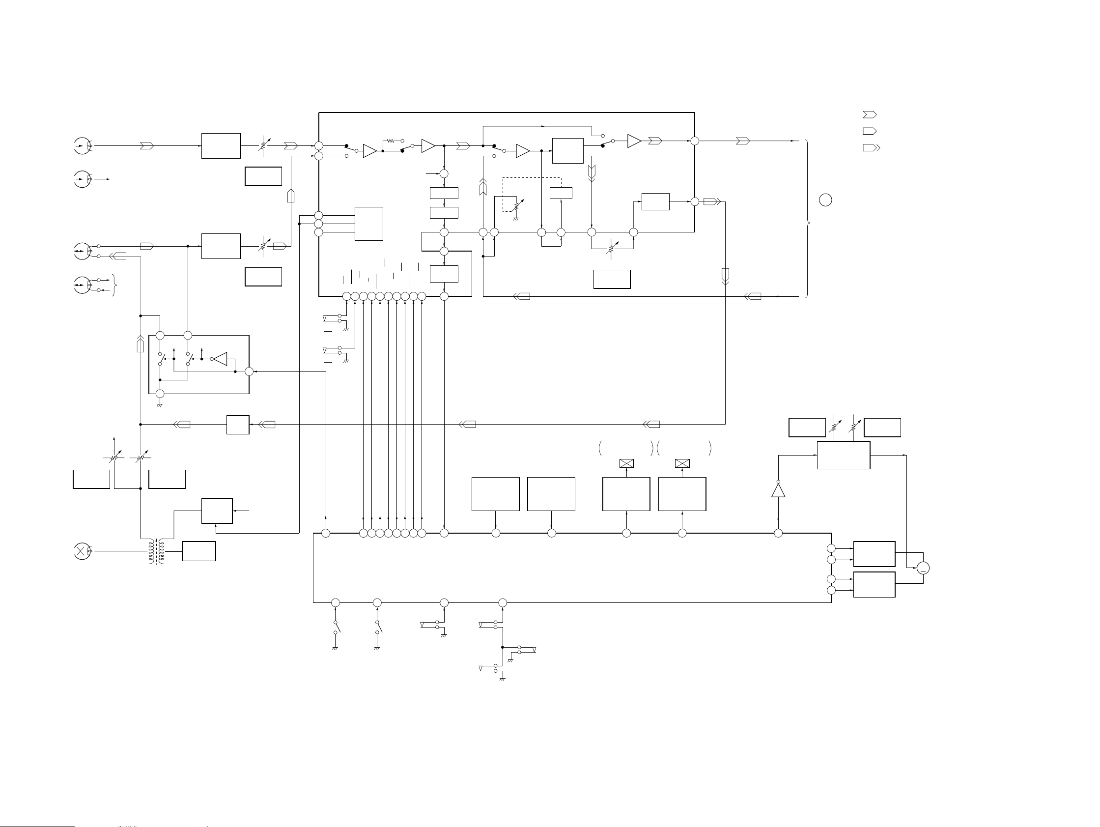
HCD-F150/FR10
6-3. BLOCK DIAGRAM — AUDIO SECTION —
HRP1
(PLAYBACK)
L-CH
R-CH R-CH
HRP2 (1/2)
(RECORD/PLAYBACK)
L-CH
R-CH R-CH
PB EQ AMP
(DECK A)
IC611
PB EQ AMP
(DECK B)
IC601
RV311
PB LEVEL (L)
(DECK A)
RV301
PB LEVEL (L)
(DECK B)
DECK PROCESS
DECK A/B SELECT, PB/REC EQ AMP,
DOLBY NR AMP, ALC, AMS
IC301
AIN (L)
48
BIN (L)
46
BIAS (N)
33
32
31
BIAS (C)
BIAS (M)
BIAS
CONTROL
CIRCUIT
B NORM/CROM
ALC ON/OFF
A 120/70
1516182022 23242517
19
NORM/HIGH
PB A/B
70
120
R-CH
NR ON/OFF
BIAS ON/OFF
RM ON/OFF
L.P.F.
BUFFER
AMS
CIRCUIT
REC/PB/PASS
LM ON/OFF
+
MAOUT
28
27
MSIN
26
MSOUT
RIN (L)
43
ALC (L)
44
DOLBY PASS
ROUT (L)
ALC
35 34
DOLBY NR
AMP
CIRCUIT
ALC
IN (L)
REC OUT (L)
39
RV301
REC LEVEL (L)
(DECK B)
EQ IN (L)
38
REC
EQ AMP
PB OUT (L)
EQ OUT
• SIGNAL PATH
: PLAYBACK (DECK A)
40
(L)
36
PB-L
REC-L
A
TO/FROM
MAIN
BLOCK
(Page 29)
: PLAYBACK (DECK B)
: RECORD
RV441
REC BIAS (R)
(DECK B)
HRP2 (2/2)
(ERASE)
R-CH
3
2
RV341
REC BIAS (L)
(DECK B)
BIAS OSC
T621
R-CH
REC/PB SWITCHING
IC602
1
R-CH
REC BIAS
SWITCH
Q623
BIAS OSC
Q621, 622
C331, L331
BIAS
TRAP
4
(A+7V)
S1004
(DECK A 120/70)
S1008
(DECK B 120/70)
RV1001
TAPE SPEED
82
CAP-M-H/L
(HIGH)
CAPM-CNT1P
CAPM-CNT2P
CAPM-CNT1M
CAPM-CNT2M
CAPSTAN MOTOR
CONTROL SWITCH
Q1001
17
77
85
86
SL1
TRIGGER PLUNGER
DECK A
ROTATION
DETECT SENSOR
(DECK A)
B+
TC-MUTE
R/P-PASS
31
AMS-IN
A-HALF
98
97
TC-RELAY
A-PLAY-SW
95 96
9994939290 898887
BIAS
PB-A/B
EQ-H/N
REC-MUTE
ALC-ON/OFF
NR-ON/OFF
B-PLAY-SW
IC1001
26
A-SHUT
B-HALF
28
ROTATION
DETECT SENSOR
(DECK B)
IC1002
27
B-SHUT
TRIGGER
PLUNGER DRIVE
(DECK A)
Q333, 334
84
SYSTEM CONTROLLER
IC501 (2/3)
A-TRG
SL2
TRIGGER PLUNGER
DECK B
TRIGGER
PLUNGER DRIVE
(DECK B)
Q331, 332
83
B-TRG
Q335
RV1002
TAPE SPEED
(NORMAL)
CAPSTAN
MOTOR DRIVE
Q336 – 339
CAPSTAN
MOTOR DRIVE
Q340 – 343
M
M1
(CAPSTAN)
S1003
(DECK A HALF)
16
S1001
(DECK A PLAY)
S1002
(DECK B PLAY)
— 31 —
S1006
(DECK B HALF)
S1009
(DECK B REC)
S1005
(DECK A REC)
— 32 —
Page 29
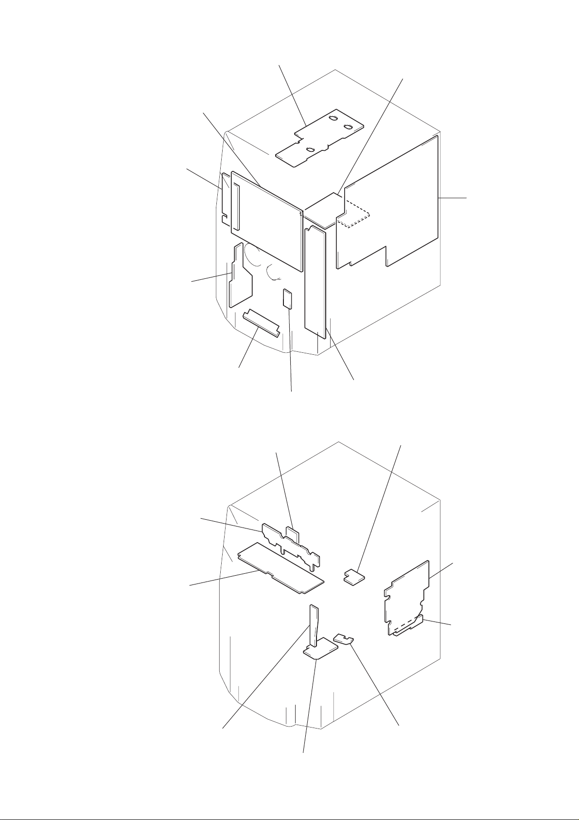
d
6-4. CIRCUIT BOARDS LOCATION
PANEL board
SW/POWER board
HP/MIC board
TRANS board
AMPLIFIER board
MAIN board
LEAF SW board
AUDIO board
DOOR LED board
CD MOTOR board
FUNC board
CD DOOR board
DISC SENSOR (S) board
BU board
DOOR SW boar
CD LED board
DISC SENSOR (R) board
TABLE SENSOR board
— 33 —
Page 30

THIS NOTE IS COMMON FOR PRINTED WIRING
BOARDS AND SCHEMATIC DIAGRAMS.
(In addition to this necessary note is printed in each
block.)
For schematic diagrams.
Note:
• All capacitors are in µF unless otherwise noted. pF: µµF
50 WV or less are not indicated except for electrolytics
and tantalums.
• All resistors are in Ω and
specified.
• % : indicates tolerance.
¢
•
• 2 : nonflammable resistor.
• 1 : fusible resistor.
• C : panel designation.
• U : B+ Line.
• V : B– Line.
• H : adjustment for repair.
• Voltages and waveforms are dc with respect to ground
• Voltages are tak en with a V OM (Input impedance 10 MΩ).
• Wavefor ms are taken with a oscilloscope.
• Circled numbers refer to waveforms.
• Signal path.
• Abbreviation
: internal component.
Note:
The components identified by mark ! or dotted
line with mark ! are critical for safety.
Replace only with part
number specified.
under no-signal (detuned) conditions.
Voltage variations may be noted due to normal produc-
tion tolerances.
F : FM
g : VIDEO/MD
E : PB (DECK A)
d : PB (DECK B)
G : REC (DECK B)
J : CD
c : CD DIGITAL
CND : Canadian
1
4
/
W or less unless otherwise
Note:
Les composants identifiés par
une marque ! sont critiques
pour la sécurité.
Ne les remplacer que par une
piéce portant le numéro
spécifié.
For printed wiring boards.
Note:
• X : parts extracted from the component side.
¢
•
• b : Pattern from the side which enables seeing.
: internal component.
— 34 —
Page 31
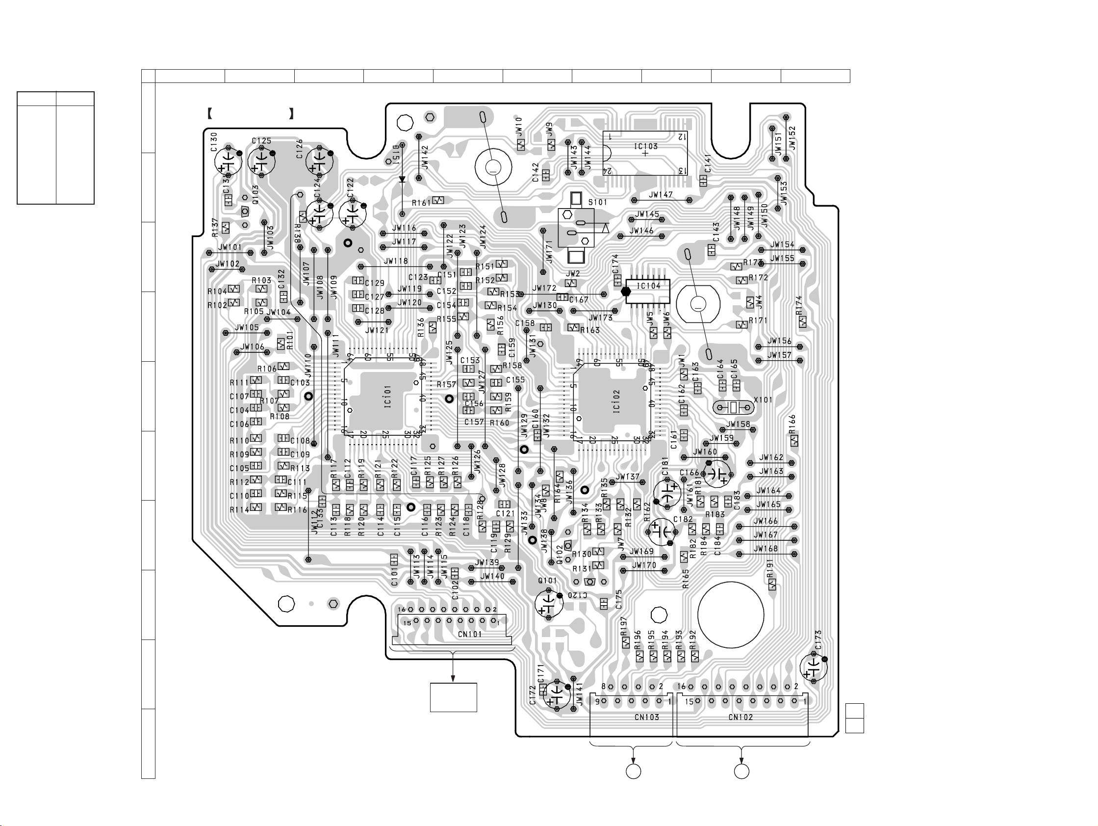
HCD-F150/FR10
6-5. PRINTED WIRING BOARD — BD SECTION — • See page 33 for Circuit Boards Location.
• Semiconductor
Location
Ref. No. Location
D151 B-4
IC101 E-4
IC102 E-7
IC103 B-8
IC104 C-8
Q101 H-6
Q102 G-6
Q103 B-2
12
A
B
C
D
BD BOARD
E
345678910
M101
SPINDLE
MOTOR
TP
(VC)
M
(LIMIT)
M102
SLED
MOTOR
M
E
F
G
H
I
TP
(TE)
TP
(FE)
TP
(RF)
TP
(TOFF)
TP
(DVDD)
JW135
E
TP
(PLCK)
E
J
OPTICAL
PICK-UP
TO
MAIN BOARD
M
CN402
(Page 52)
N
TO
MAIN BOARD
CN401
(Page 52)
— 35 — — 36 —
1-664-
353-
12
(12)
Page 32
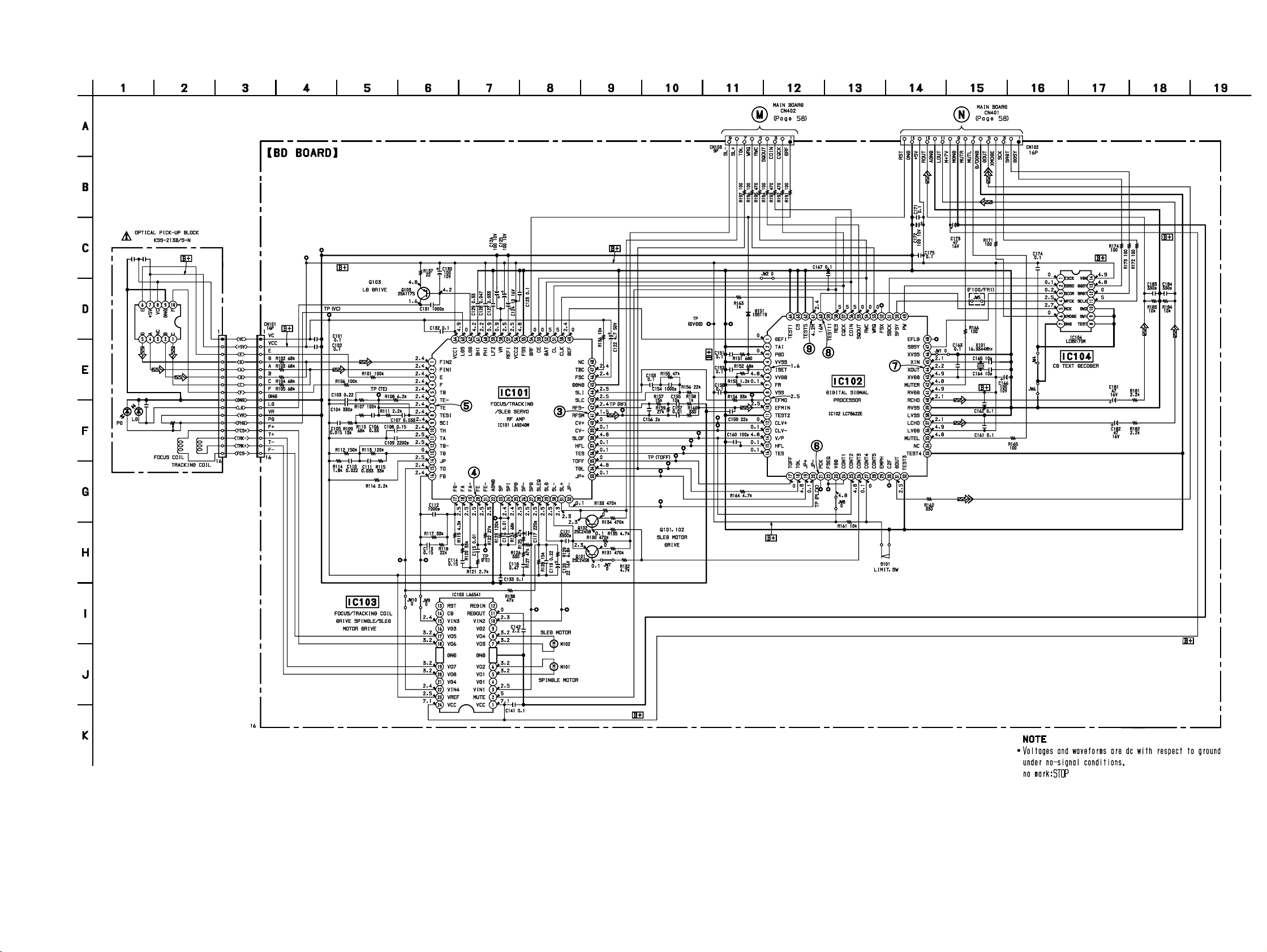
6-6. SCHEMATIC DIAGRAM — BD SECTION — • See page 71 for Waveforms. • See page 72 for IC Pin Functions.
HCD-F150/FR10
— 37 — — 38 —
Page 33
HCD-F150/FR10
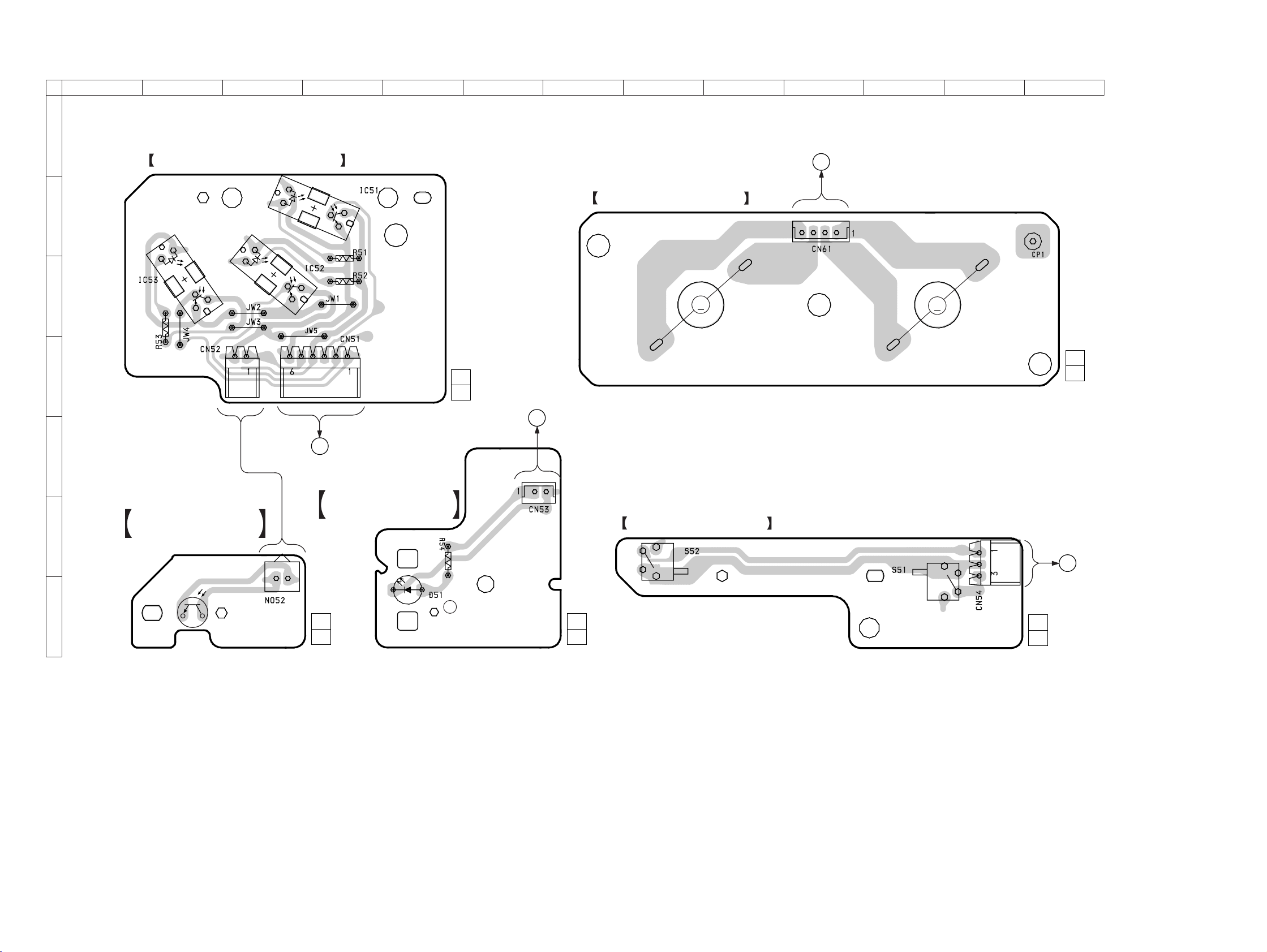
6-7. PRINTED WIRING BOARD — CD MOTOR SECTION — • See Page 33 for Circuit Boards Location.
12
A
B
C
D
E
345678910111213
TABLE SENSOR BOARD
MAIN BOARD
J
TO
CN451
(Page 52)
1-663-971-
11
(11)
TO
MAIN BOARD
CN453
(Page 52)
I
CD MOTOR BOARD
M62
TABLE MOTOR
M
TO
MAIN BOARD
CN461
(Page 52)
L
M61
LOADING MOTOR
M
1-663-974-
11
(11)
F
G
DISC SENSOR (R)
BOARD
Q51
1
1-663-972-
DISC SENSOR (S)
BOARD
11
(11)
1-663-973-
11
(11)
DOOR SW BOARD
(DOWN)
(UP)
1-663-975-
TO
MAIN BOARD
CN454
(Page 52)
K
11
(11)
— 39 — — 40 —
Page 34
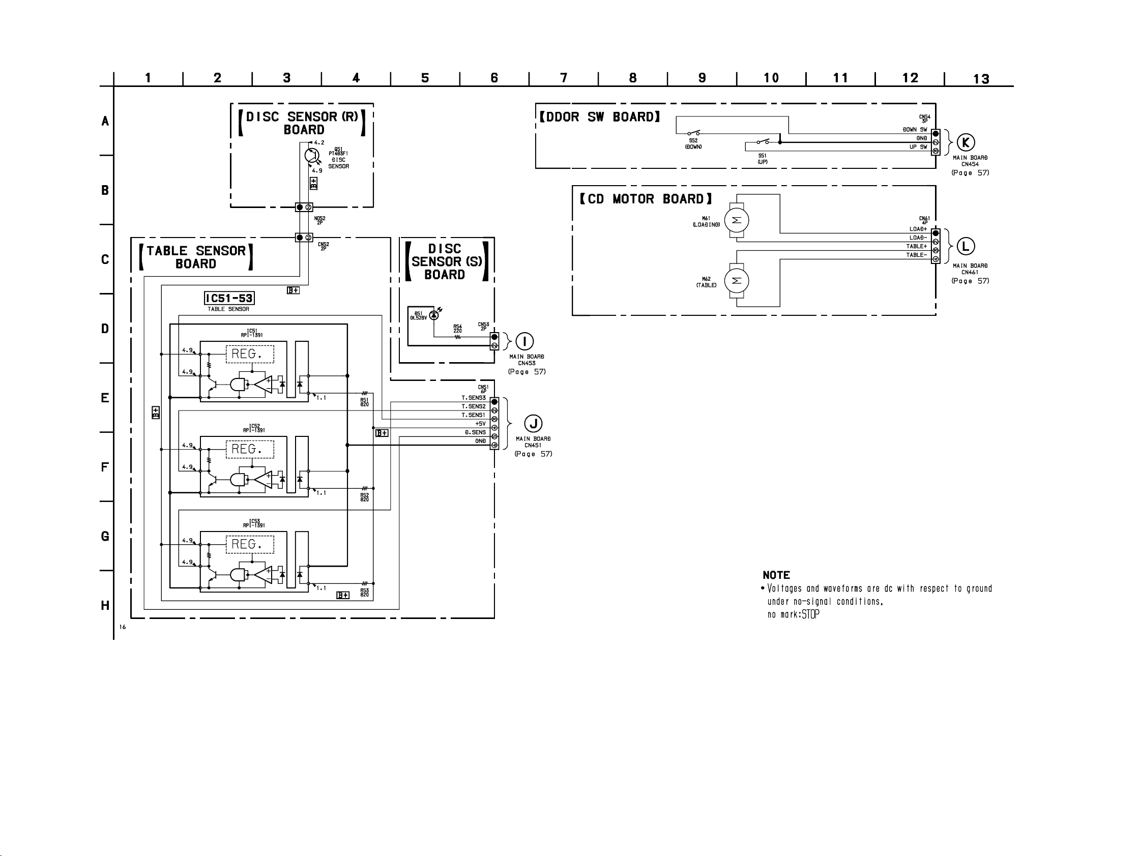
6-8. SCHEMATIC DIAGRAM — CD MOTOR SECTION —
HCD-F150/FR10
— 41 — — 42 —
Page 35
HCD-F150/FR10
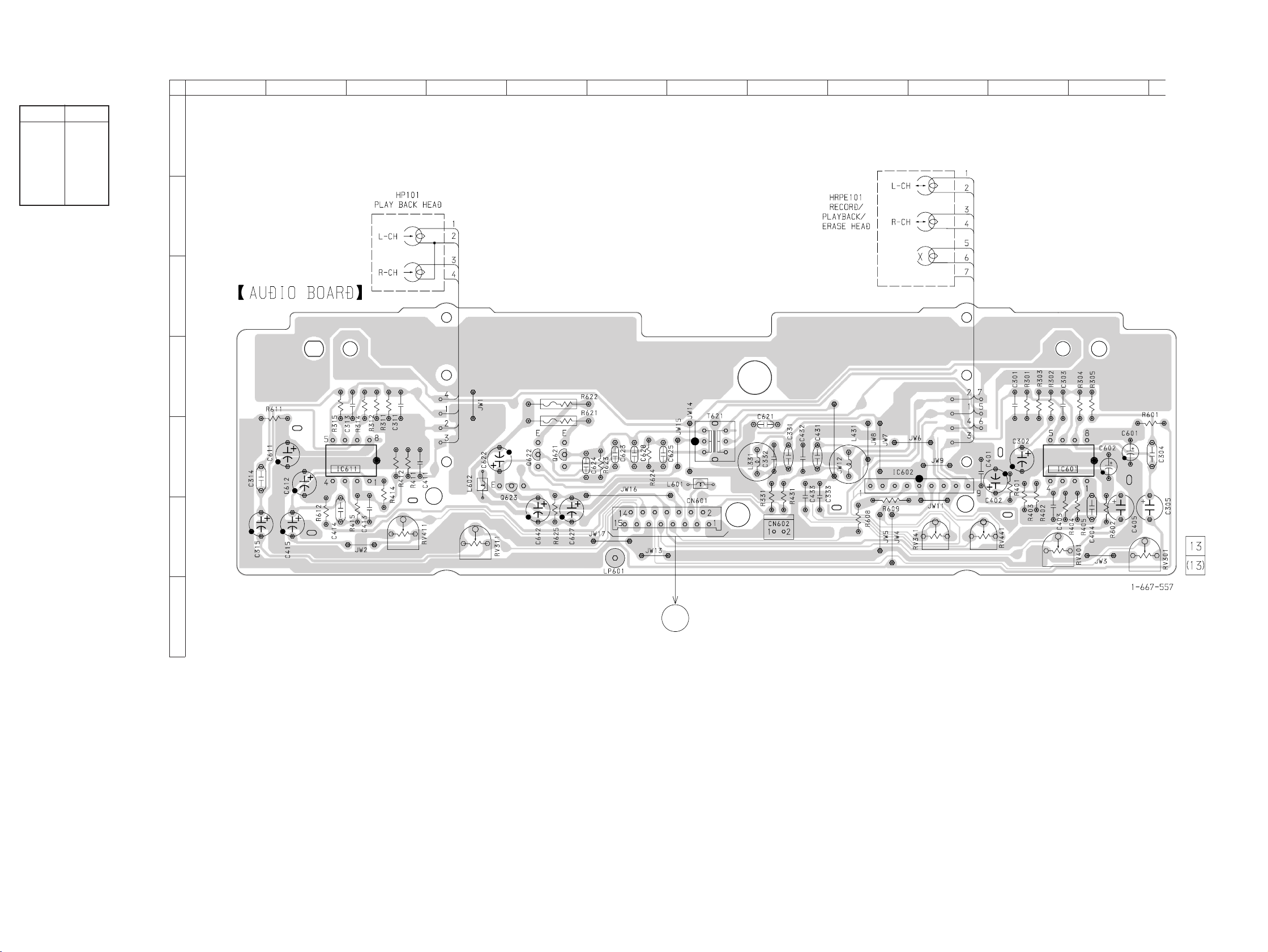
6-9. PRINTED WIRING BOARD — AUDIO SECTION — • See page 33 for Circuit Boards Location.
• Semiconductor
Location
Ref. No. Location
IC601 E-12
IC602 E-9
IC611 E-2
Q621 E-5
Q622 E-5
Q623 E-5
12
A
B
C
D
3456789101112
E
F
16
G
P
MAIN BOARD
CN106
(Page 51)
— 43 — — 44 —
Page 36
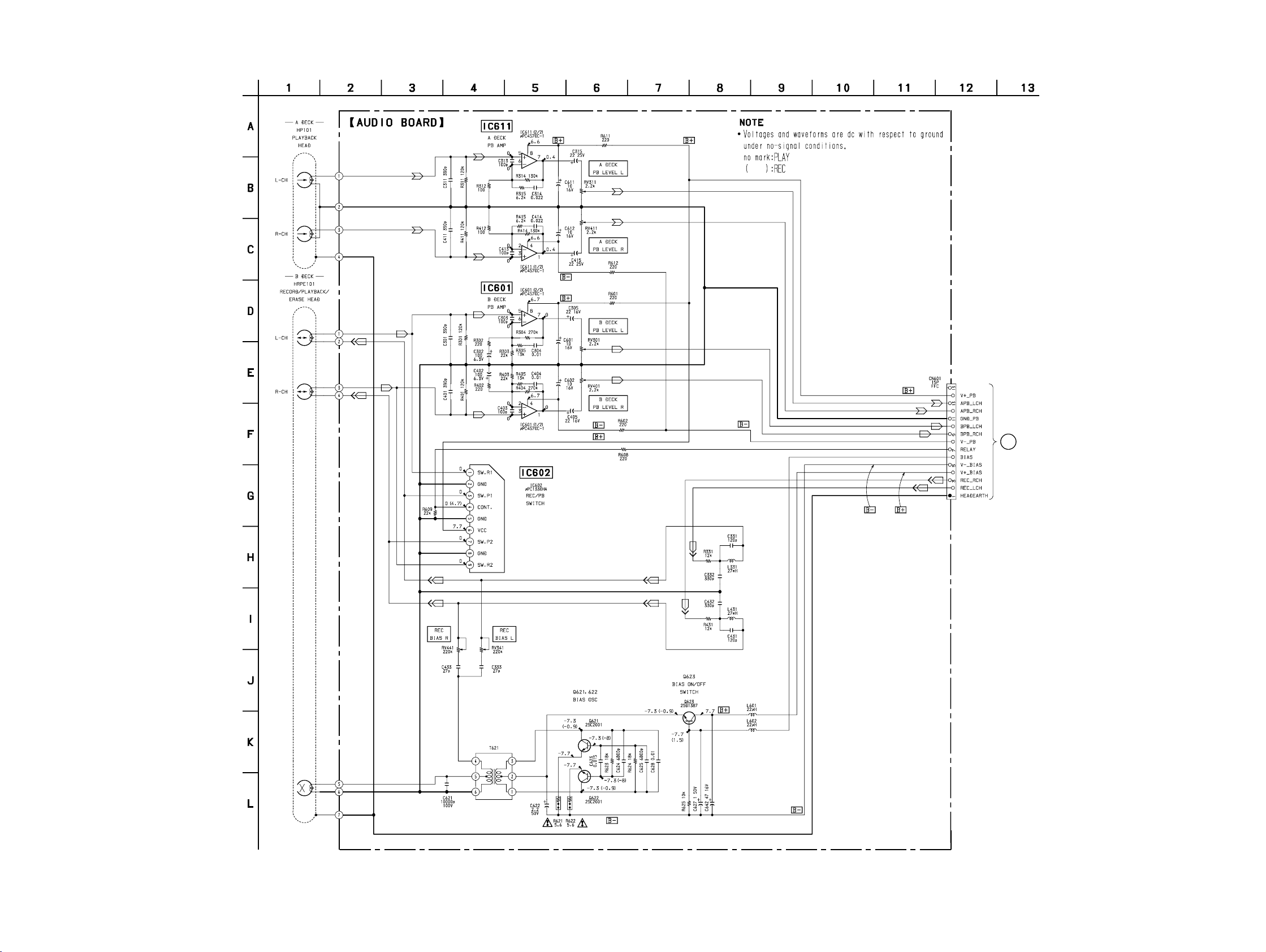
6-10. SCHEMATIC DIAGRAM — AUDIO SECTION —
HCD-F150/FR10
MAIN BOARD
P
(Page 55)
CN106
16
— 45 — — 46 —
Page 37
HCD-F150/FR10
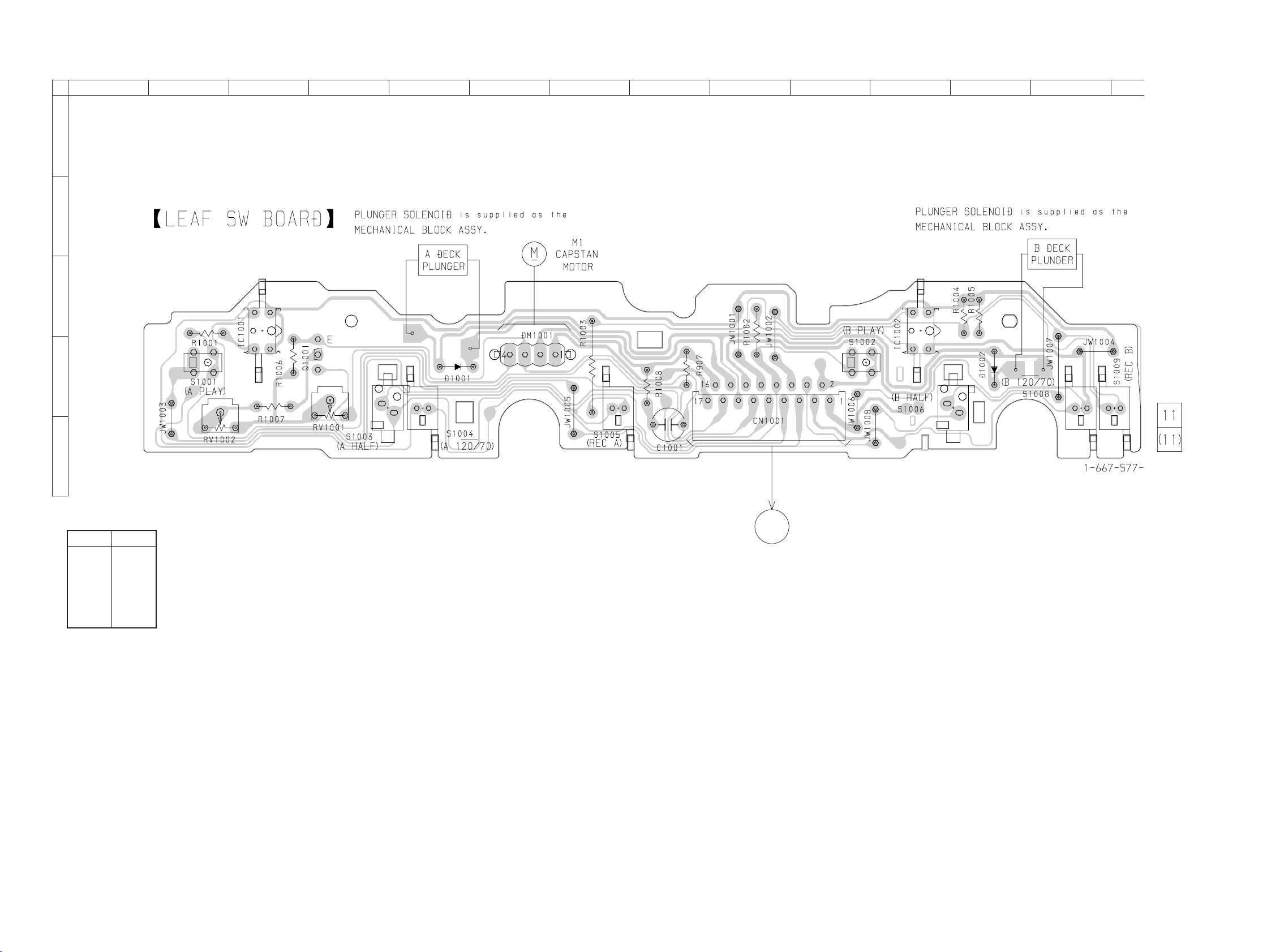
6-11. PRINTED WIRING BOARD — LEAF SW SECTION — • See page 33 for Circuit Boards Location.
12
A
B
C
D
345678910111213
E
• Semiconductor
Location
Ref. No. Location
D1001 D-5
D1002
IC1001 C-3
IC1002 C-11
Q1001 D-4
16
MAIN BOARD
Q
(Page 51)
CN107
— 47 — — 48 —
Page 38
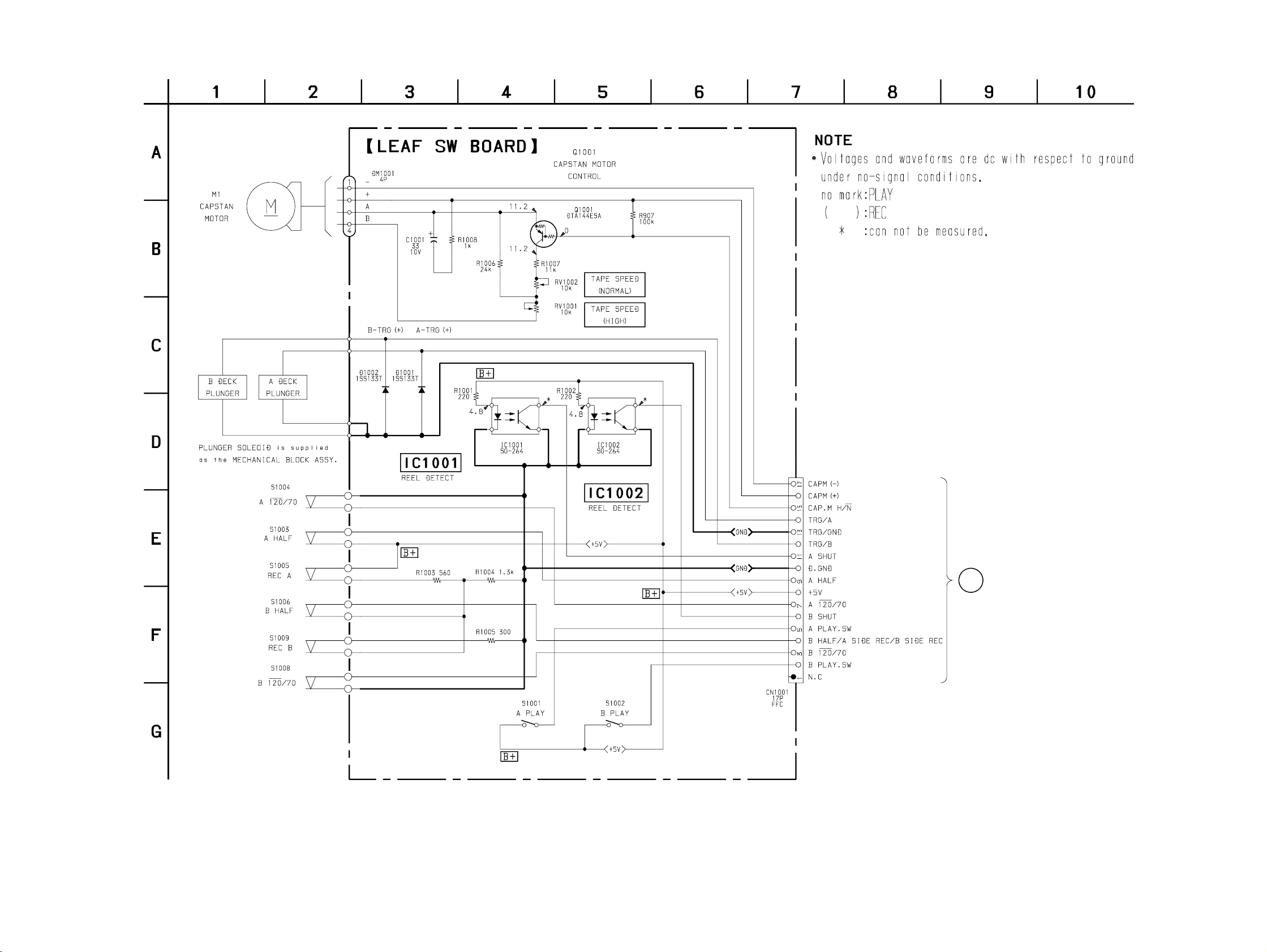
6-12. SCHEMATIC DIAGRAM — LEAF SW SECTION —
(Page 55)
MAIN BOARD
CN107
Q
16
HCD-F150/FR10
— 49 — — 50 —
Page 39
HCD-F150/FR10
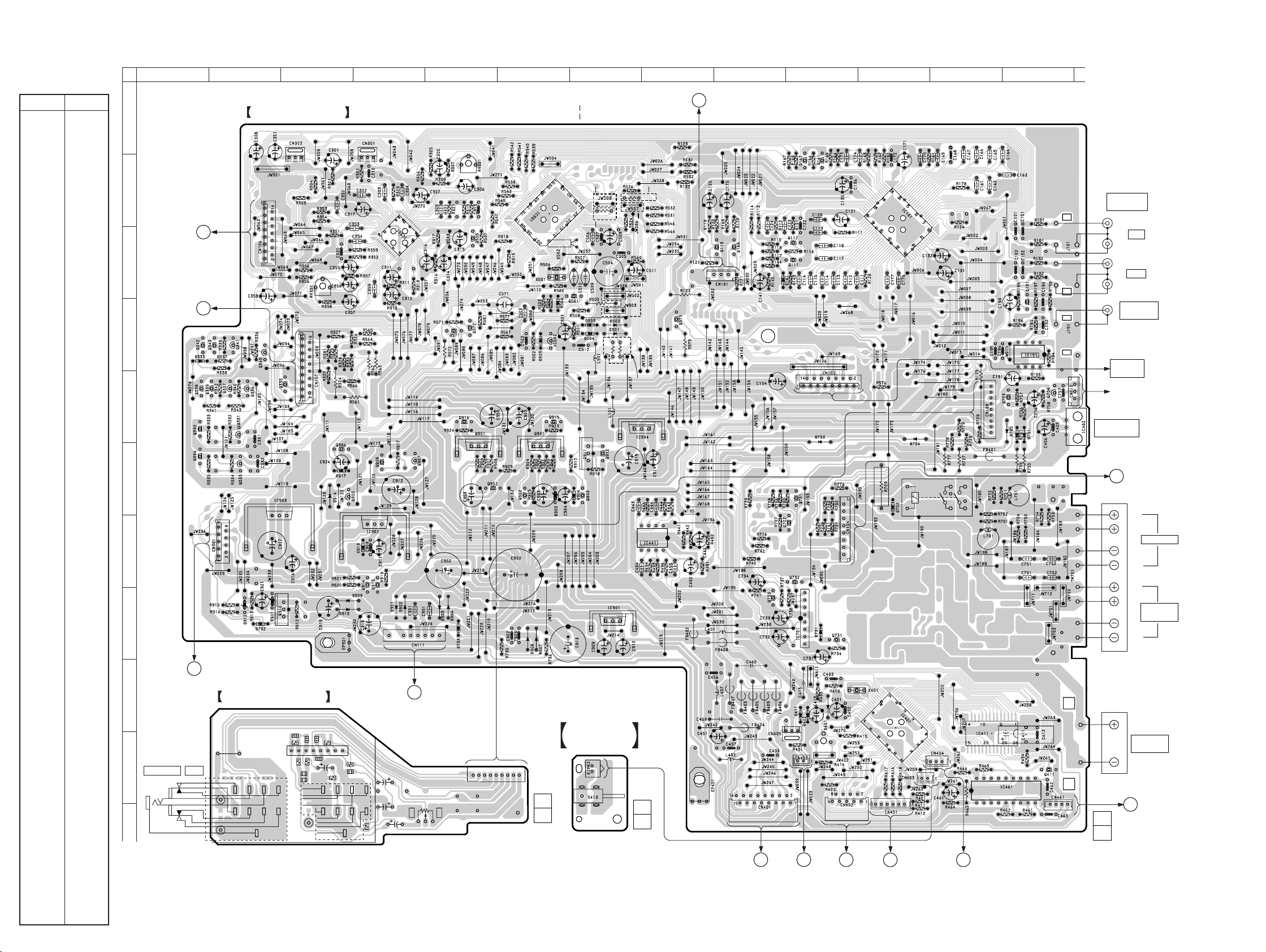
6-13. PRINTED WIRING BOARD — MAIN SECTION — • See page 33 for Circuit Boards Location.
• Semiconductor
Location
Ref. No. Location
D141 C-10
D333 D-1
D401 I-10
D402 I-10
D411 I-10
D501 D-7
D502 D-7
D503 D-7
D504 D-7
D505 D-6
D506 D-6
D701 E-13
D702 F-11
D703 E-10
D704 E-11
D705 E-13
D712 G-11
D731 H-10
D732 H-2
D733 H-5
D751 E-11
D901 H-4
D902 H-4
D903 H-5
D904 H-5
D905 F-6
D906 F-7
D907 I-6
D908 I-6
D909 H-4
D910 H-3
D911 H-2
D912 H-2
D913 G-4
D914 F-3
D917 F-3
IC101 B-11
IC191 D-13
IC301 C-4
IC401 I-11
IC402 E-13
IC411 I-12
IC441 G-8
IC461 J-13
IC501 B-6
IC502 D-6
IC701 H-10
IC901 H-7
IC902 G-4
IC903 F-2
IC904 E-8
Q111 C10
Q112 B-10
Q113 C-9
Q191 C-13
Q161 B-10
Q162 B-10
Q163 C-9
Q331 E-2
Q332 E-1
Q333 F-2
Q334 F-1
Q335 E-3
Q336 E-2
Q337 E-2
Q338 E-1
Q339 E-1
Q340 D-2
Q341 D-2
Q342 D-1
Q343 D-1
Q411 J-13
Q501 D-7
Q505 C-5
Q571 D-5
Q572 D-5
Q575 D-8
Q701 F-10
Q702 F-10
Q703 E-13
Q704 E-13
Q711 G-9
Q712 F-9
Q713 F-9
Q731 H-10
Q732 G-10
Q733 H-9
Q901 E-6
Q902 F-6
Q903 F-7
Q905 F-4
Q906 F-3
Q907 F-4
Q908 F-4
Q910 H-2
Q911 F-7
Q912 F-7
Q913 G-4
Q914 G-4
Q915 E-6
Q916 E-5
Q951 E-5
Q952 F-5
12
A
B
C
(Page 44)
AUDIO BOARD
CN601
(Page 48)
LEAF SW BOARD
CN1001
D
E
F
G
H
I
J781
J
PHONES
J782
MIC
K
16
TO
P
TO
Q
EEE
EEE
E
E
PANEL BOARD
A
TO
CN601
(Page 64)
E
E
HP/MIC BOARD
J781
345678910111213
TO
NO801
(Page 68)
EE
TO
BD BOARD
CN102
(Page 36)
E
E
E
(N.C)
N
TO
DISC SENSOR(S)
BOARD
CN53
(Page 39)
EE
40
41
E
E
1
8
E
8
1
E
40
41
IMJ
TO
BD BOARD
CN103
(Page 36)
MAIN BOARD
(N.C)
E
E
E
E
C784
R785
R784
C782
13
C783
C786
R788
C789
R782
R783
C781
J782
R781
(N.C)
E
E
3
EE
IC781
R787
C790
56
1
1
C799
C788
R789
43
14
E
1
C785
42
15
29
28
E
7
TO
TRANS BOARD
E
CN993
(Page 68)
RV781
51
80
81
E
E
E
E
E
19
NO781
100
1
EE
11
1-669-648-
(11)
X1:FR10:AEP,UK,G,AUS MODEL
X2:F150/FR10:SP,MY MODEL
50
31
30
R512
X1
E
1
3
E
R522
E
E
EE
CD DOOR
BOARD
1-669-650-
X1X2
R511
X2
F150/FR10:AUS,
SP,MY
MODEL
R523
FR10:AEP,
UK,G
MODEL
13
58
1
4
13
11
(11)
AMPLIFIER BOARD
B
E
— 51 — — 52 —
25
24
1
80
65
64
RY701
24
25
1
80
65
64
TO
TABLE SENSOR
BOARD
CN51
(Page 39)
E
58
1
4
1
E
9
19
1018
1-669-644-
K
TO
CN54
(Page 40)
DOOR SW BOARD
E
E
J101
VIDEO/MD
AUDIO
R
IN
L
R
OUT
L
J191
SUPER
WOOFER
TUNER
UNIT
FAN (FAN101)
IC402
CD DIGITAL
OUT
AMPLIFIER BOARD
C
TO
CN803
(Page 67)
TM701
R
L
SPEAKER
R
L
R
L
SPEAKER
R
L
TM702
CENTER
SPEAKER
CD MOTOR BOARD
L
11
(11)
REAR
TO
CN61
(Page 40)
Page 40
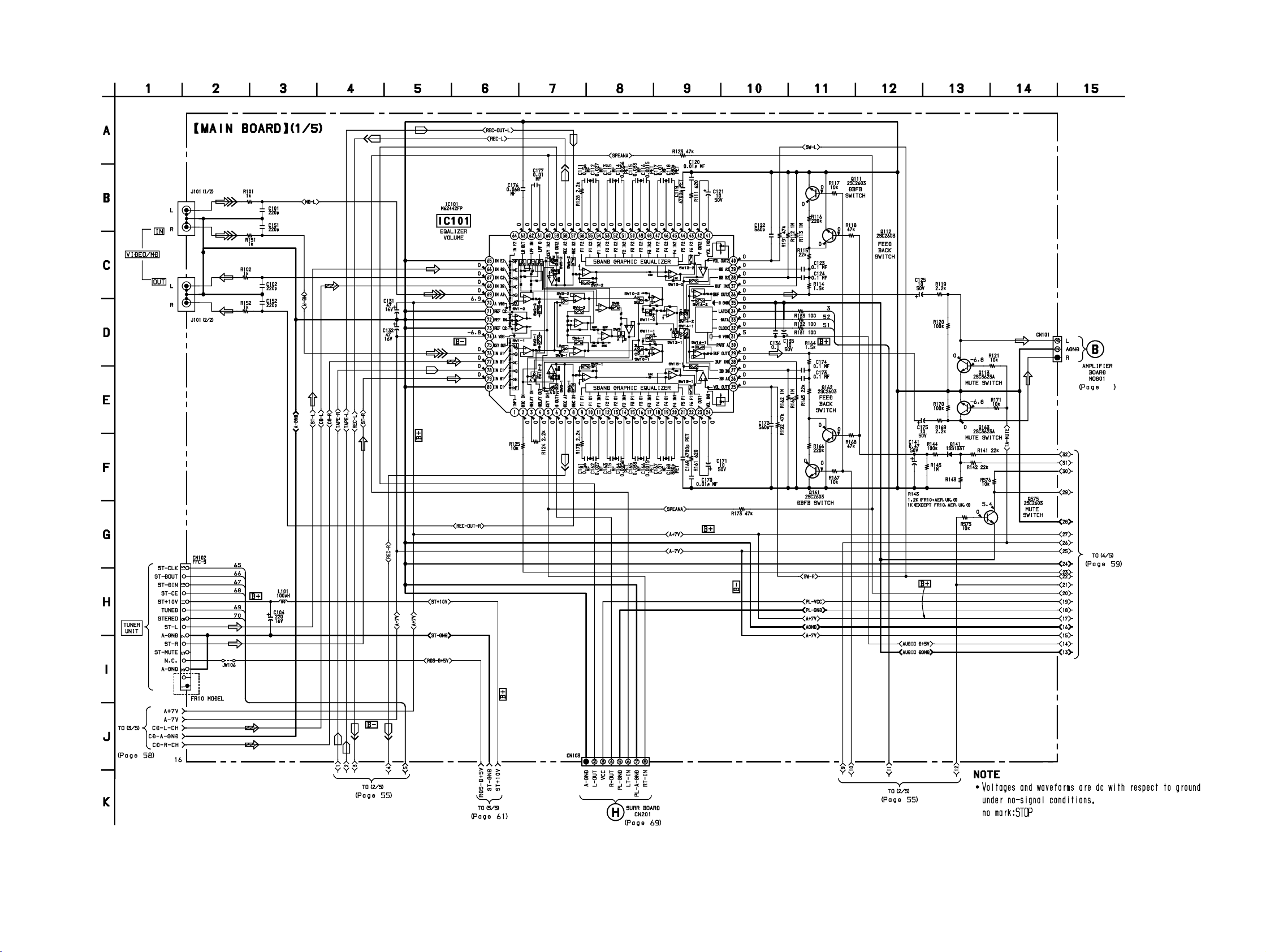
6-14. SCHEMATIC DIARGAM — MAIN (1/5) SECTION —
HCD-F150/FR10
69
— 53 — — 54 —
Page 41
HCD-F150/FR10
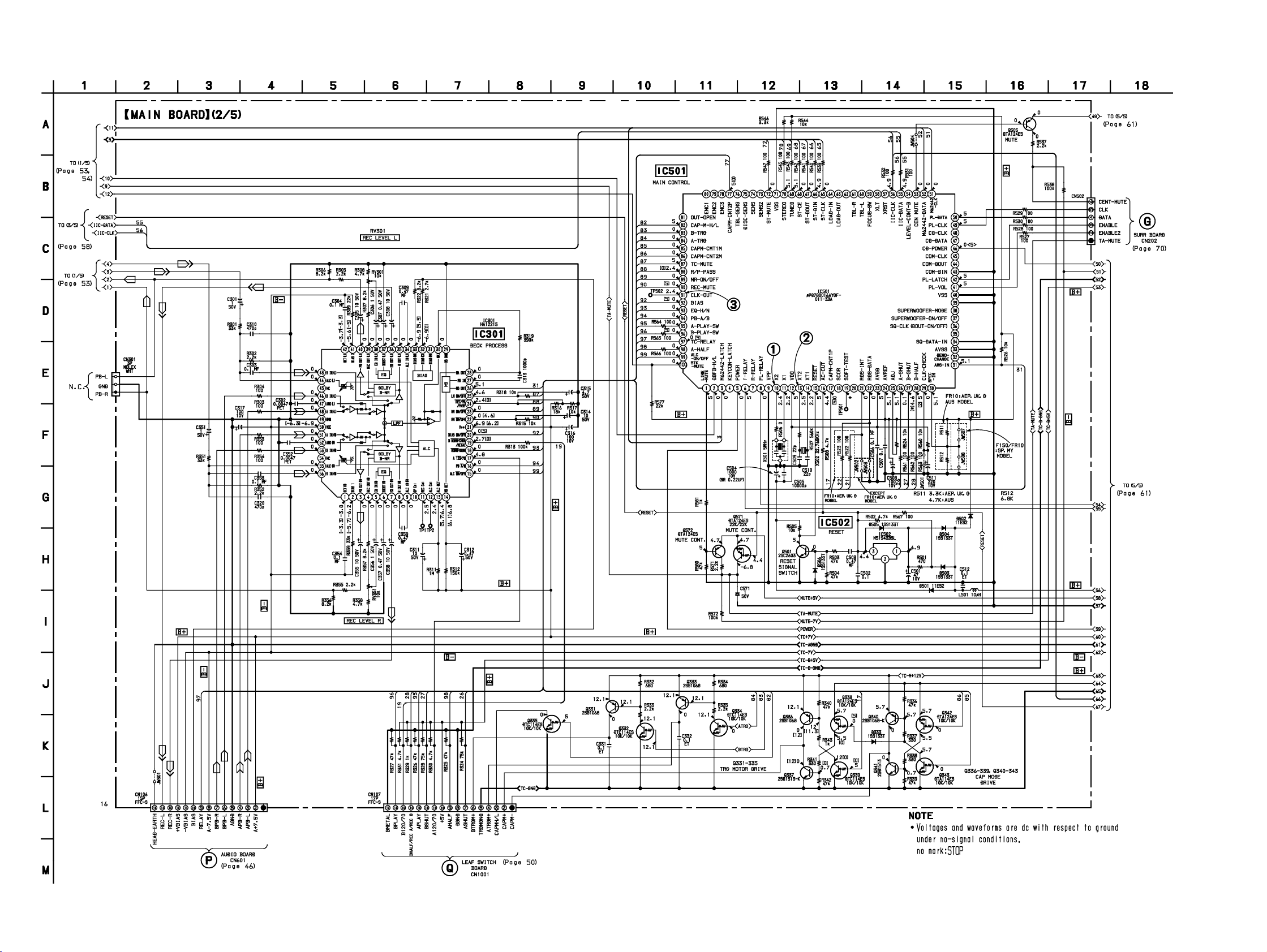
6-15. SCHEMATIC DIARGAM — MAIN (2/5) SECTION — • See page 51 for Printed Wiring Board. • See page 71 for Waveforms. • See page 77 for IC Pin Functions.
— 55 — — 56 —
Page 42
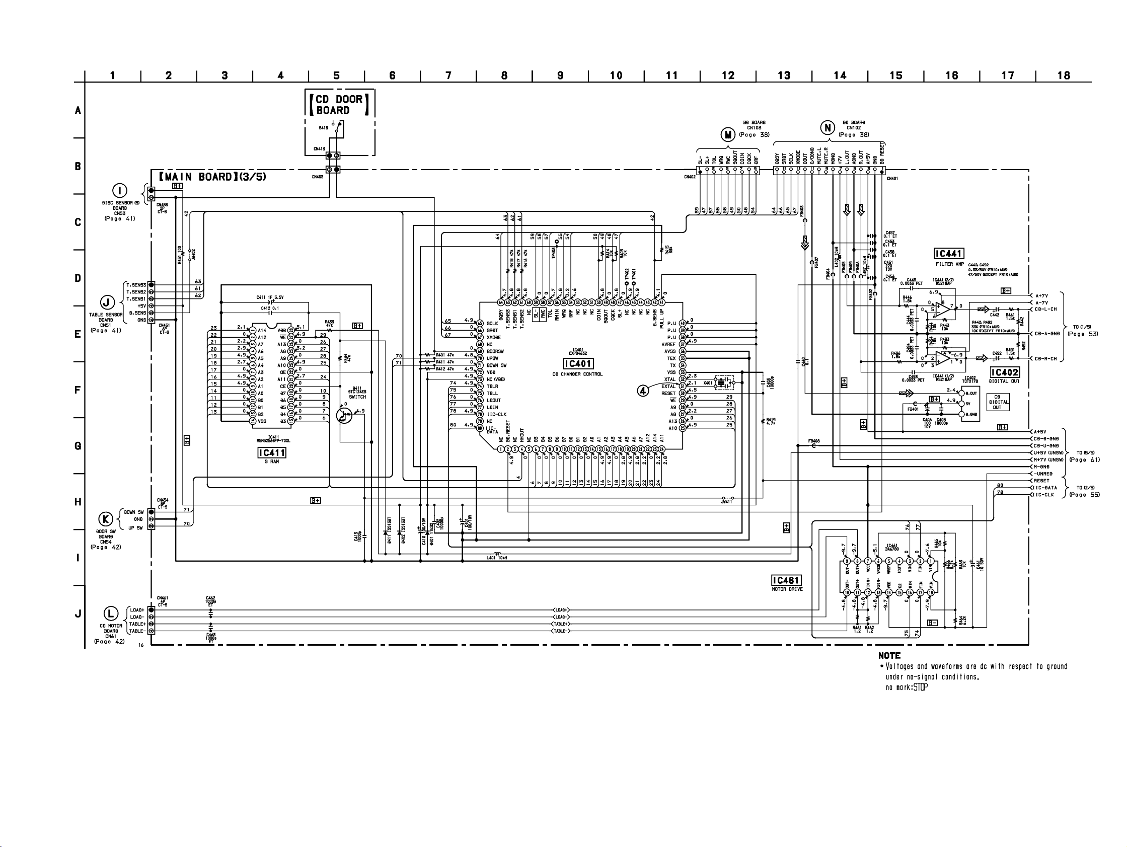
6-16. SCHEMATIC DIARGAM — MAIN (3/5) SECTION — • See page 51 for Printed Wiring Board. • See page 71 for Waveforms. • See page 76 for IC Pin Functions.
HCD-F150/FR10
— 57 — — 58 —
Page 43
HCD-F150/FR10
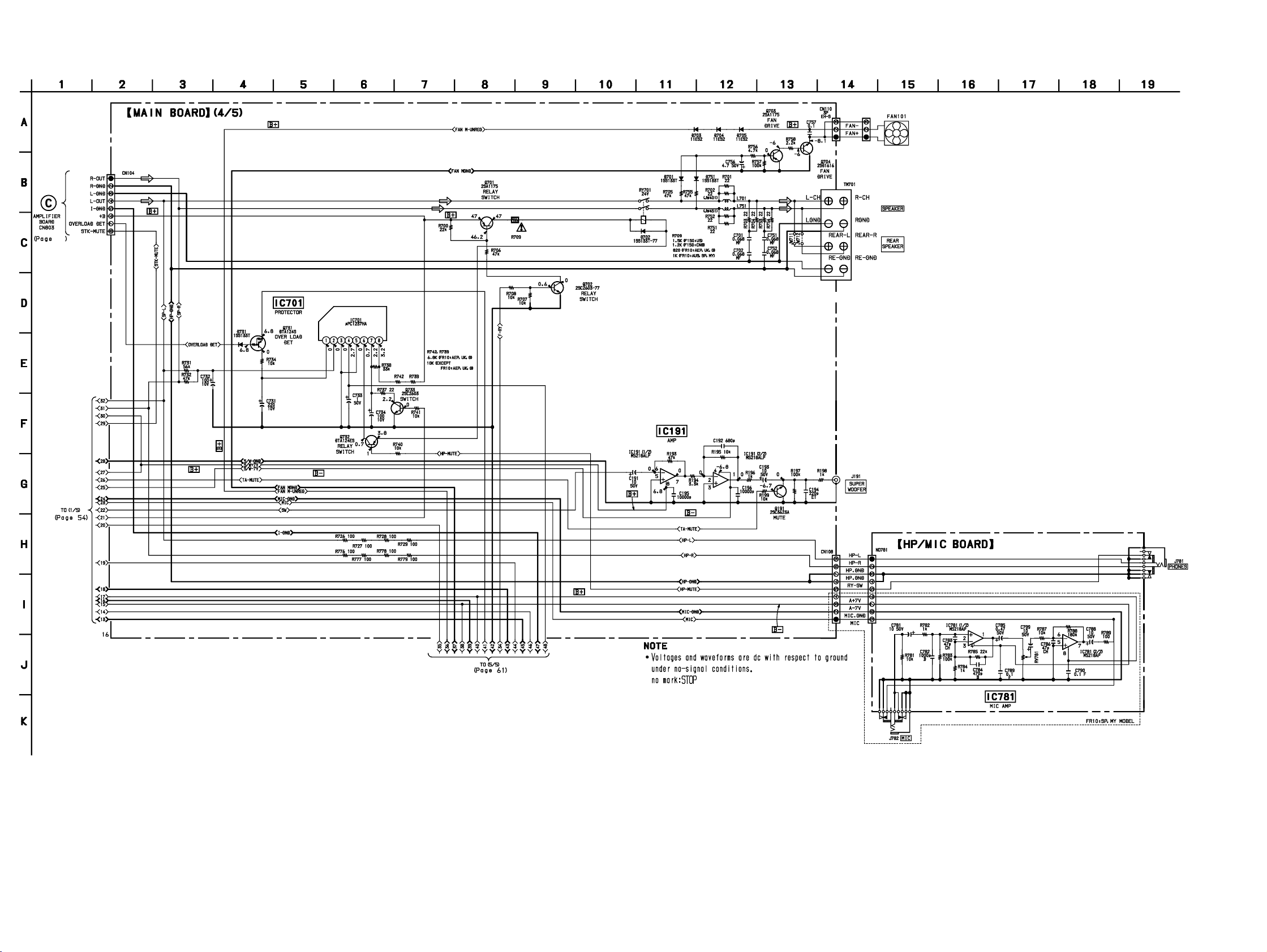
6-17. SCHEMATIC DIARGAM — MAIN (4/5) SECTION — • See page 51 for Printed Wiring Board. • See page 80 for IC Black Diagrams.
70
— 59 — — 60 —
Page 44
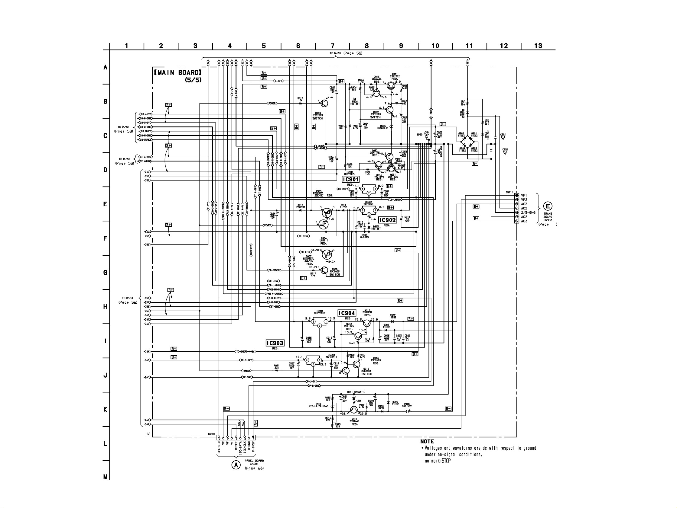
6-18. SCHEMATIC DIARGAM — MAIN (5/5) SECTION — • See page 51 for Printed Wiring Board.
HCD-F150/FR10
70
— 61 — — 62 —
Page 45
HCD-F150/FR10
A
TO
MAIN BOARD
CN501
FUNC BOARD
DOOR LED
BOARD
CD LED
BOARD
PANEL BOARD SW/POWER BOARD
PON BOARD
2
1
1-669-681-
11
(11)
1-669-651-
11
(11)
1-669-652-
11
(11)
1-669-654-
11
(11)
1-669
-646-
11
(11)
1-669-645-
11
(11)
1
10
1
2
3
VOLUME
DSP
ENTER
GROOVE
DBFB
CD
12345
GROUP ENTRY
FLASH
LOOP
CD PLUS ONE
REPEAT
CHECK
CLEAR
DELETE
FILE
SELECT
MEMO
SEARCH
MEMO
SCAN
MEMO
INPUT
DISYLAY/
DEMO
HI-SPEED
DUBBING
REC
PON
PAUSE
CD
SYNCHRD
TUNER/
BAND
CLOCK
TIMER
TIMER
SELECT
PROGRAM
SHUFFLE
CONTINUE
FUNCTION
1
10
1
5
TAPE A
TAPE A
TAPE B
TAPE B
E
1/
1
5
E
1
1
3
(JOG)
2
E
E
E
E
E
E
E
6869
65
42
FL601
17
512
16
NO609
S630
R660
NO610
(Page 51)
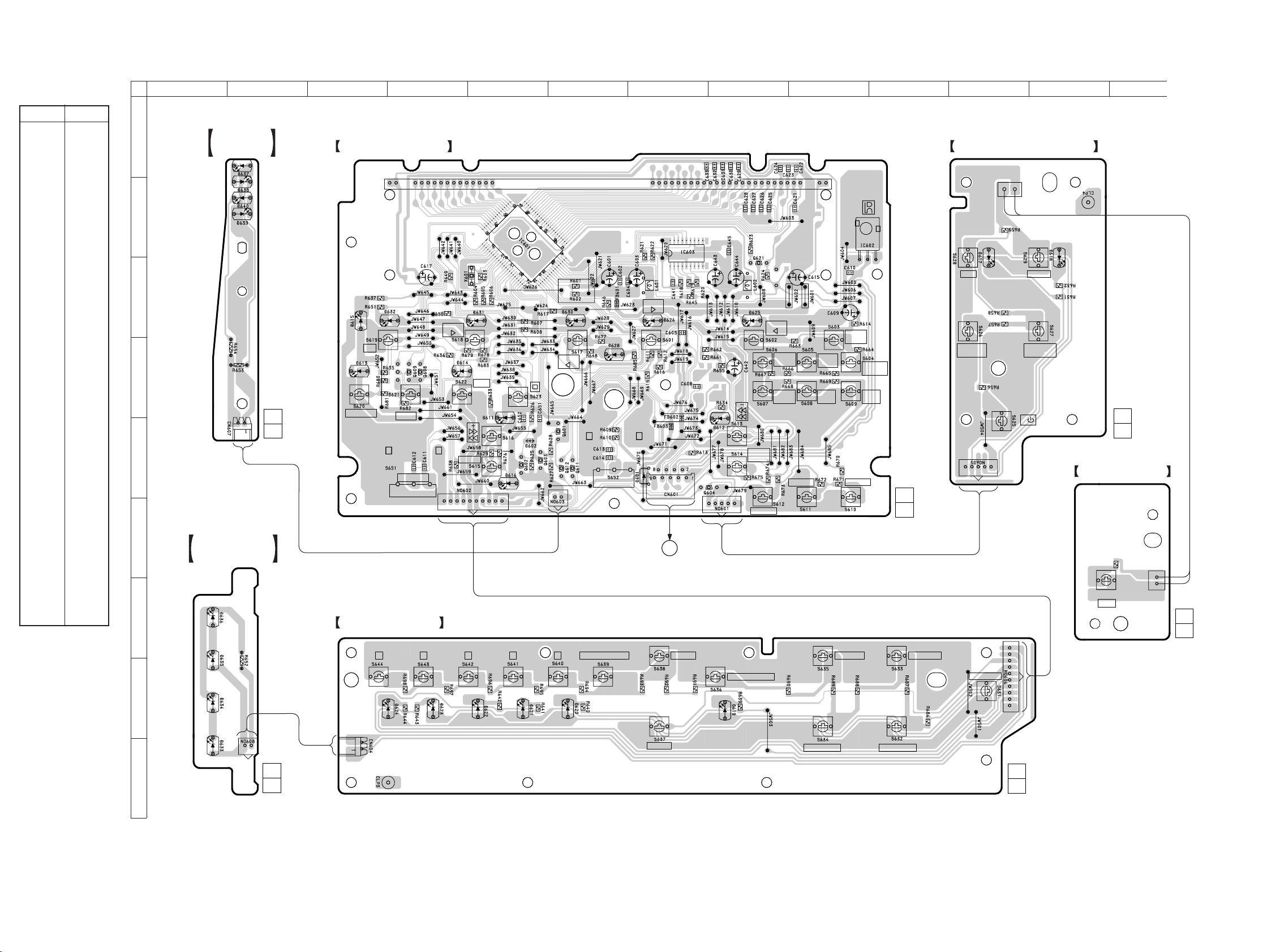
6-19. PRINTED WIRING BOARD — PANEL SECTION — • See page 33 for Circuit Boards Location.
• Semiconductor
Location
Ref. No. Location
D601 E-7
D602 E-5
D611 E-5
D612 E-8
D613 D-3
D614 D-4
D615 C-3
D616 E-5
D617 C-11
D618 B-12
D619 H-8
D620 H-6
D621 H-5
D622 H-5
D623 H-4
D624 H-3
D625 C-8
D626 C-7
D627 D-7
D628 C-6
D630 C-6
D631 C-5
D632 C-4
D633 I-1
D634 H-1
D635 H-1
D636 G-1
D637 A-2
D638 B-2
D639 B-2
D640 B-2
12
3456789101112
A
B
C
D
E
13
IC601 B-5
IC602 B-10
IC603 B-7
Q601 E-6
Q602 E-5
Q603 E-6
Q604 E-8
Q608 D-4
Q609 D-4
Q610 D-4
Q611 E-6
Q612 E-6
Q621 B-8
F
G
H
I
— 63 — — 64 —
Page 46
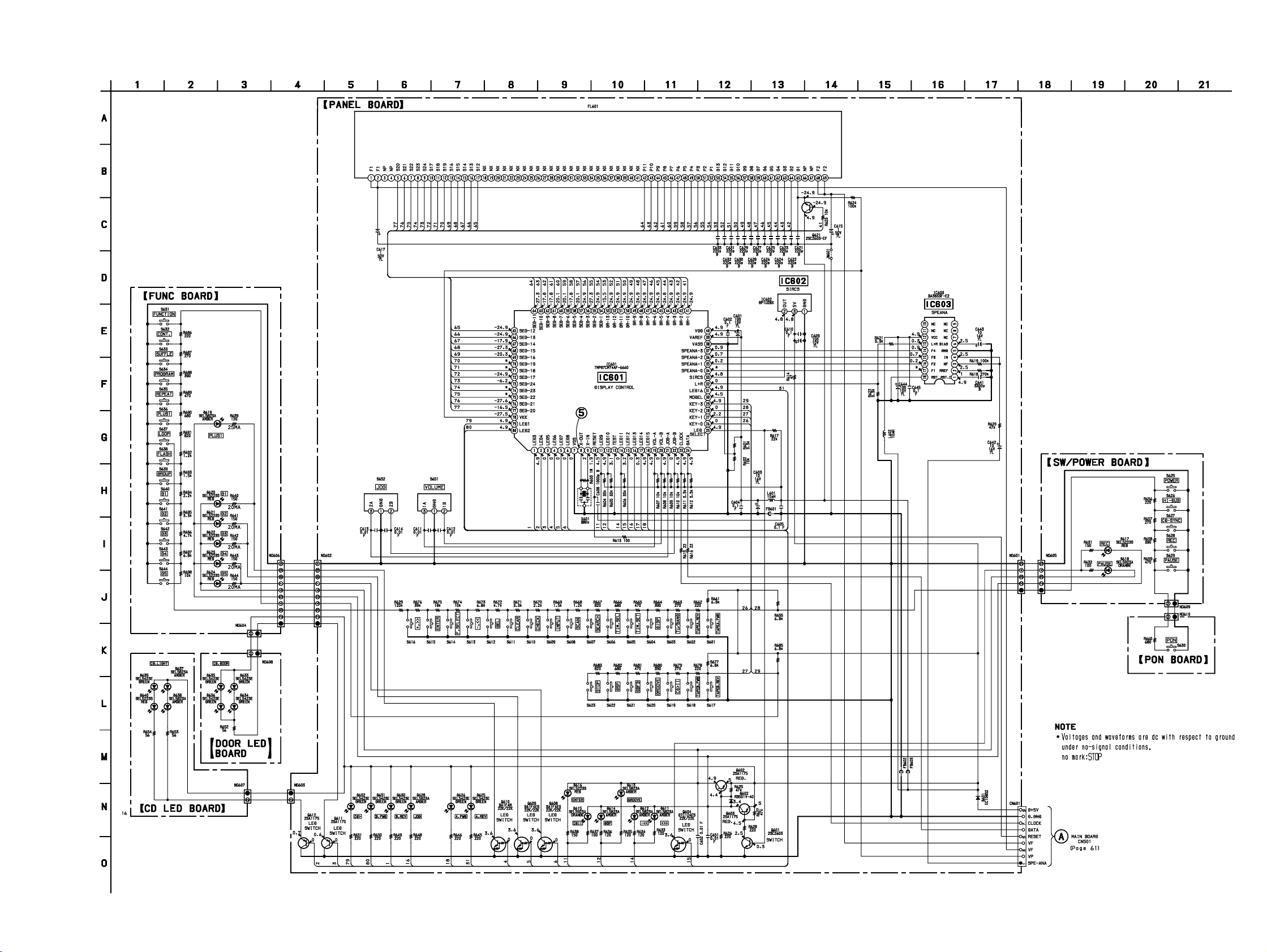
6-20. SCHEMATIC DIAGRAM — PANEL SECTION — • See page 80 for IC Black Diagrams.
HCD-F150/FR10
— 65 — — 66 —
Page 47
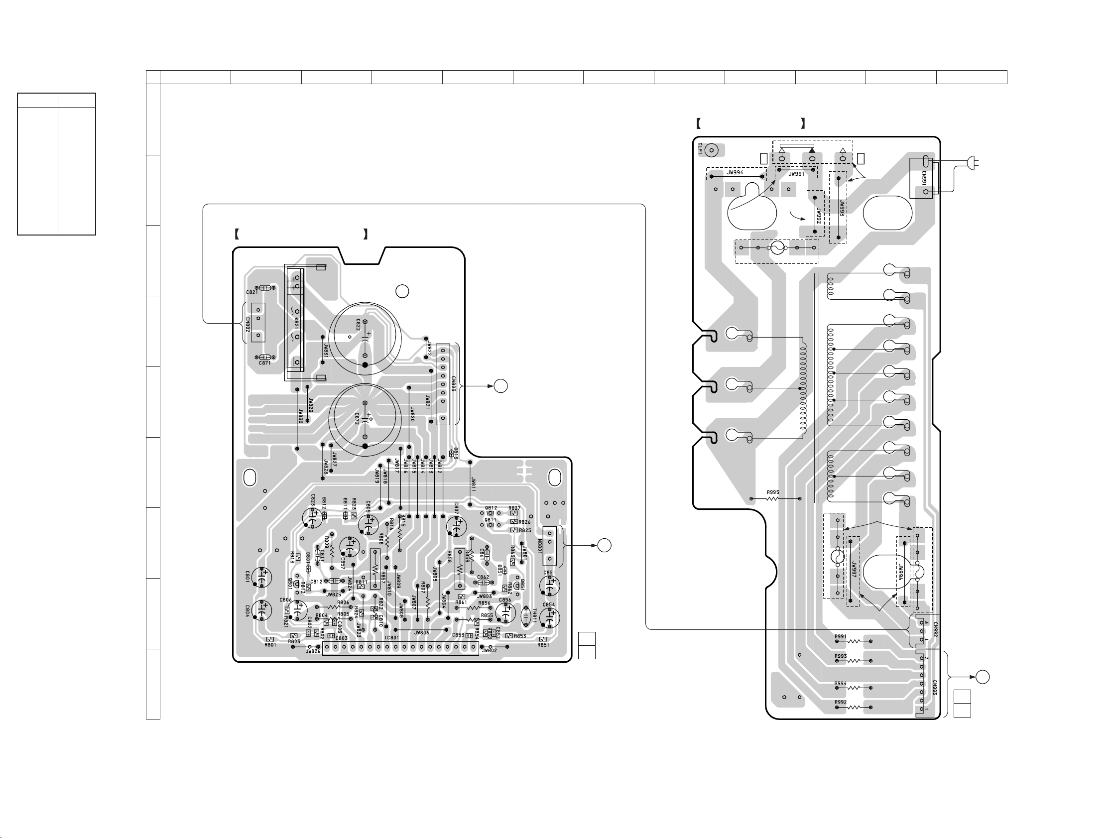
HCD-F150/FR10
6-21. PRINTED WIRING BOARD — POWER SECTION — • See page 33 for Circuit Boards Location.
• Semiconductor
Location
Ref. No. Location
D801 G-3
D811 F-3
D812 F-3
D813 F-5
D821 D-2
D851 G-6
IC801 H-4
Q801 H-2
Q811 G-5
Q812 F-5
Q851 G-6
12
A
B
C
D
3456789101112
AMPLIFIER BOARD
3
1
8
TRANS BOARD
FR10:AEP,UK,
G,SP,MY
MODEL
FR10:AEP,
UK,G,AUS
MODEL
F992
F150/FR10:AUS,SP,MY
MODEL
S991
AC
IN
FR10:SP,MY
MODEL
F150
MODEL
T991
E
F
G
H
16
I
C
TO
MAIN BOARD
1
E
118
CN104
(Page 52)
E
E
3
1
E
1-669-647-
B
TO
MAIN BOARD
CN101
(Page 52)
11
(11)
F994
FR10:AEP,UK,G,
SP,MY MODEL
F150/FR10:AUS
MODEL
1-669-649-
F993
(Page 51)
TO
MAIN BOARD
CN111
E
11
(11)
— 67 —
— 68 —
Page 48
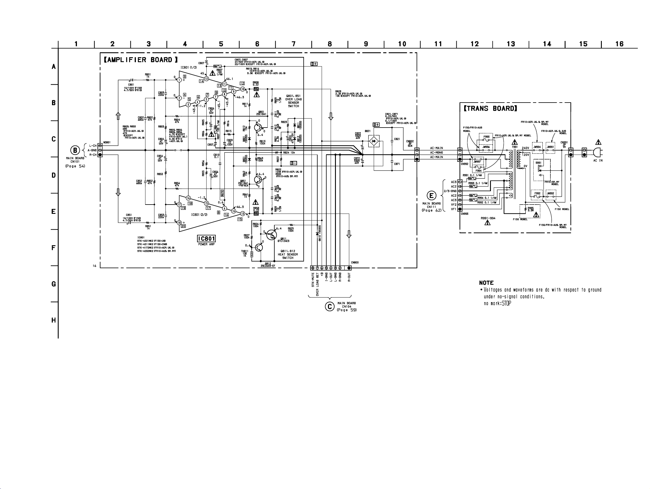
6-22. SCHEMATIC DIAGRAM — POWER SECTION —
HCD-F150/FR10
— 69 — — 70 —
Page 49
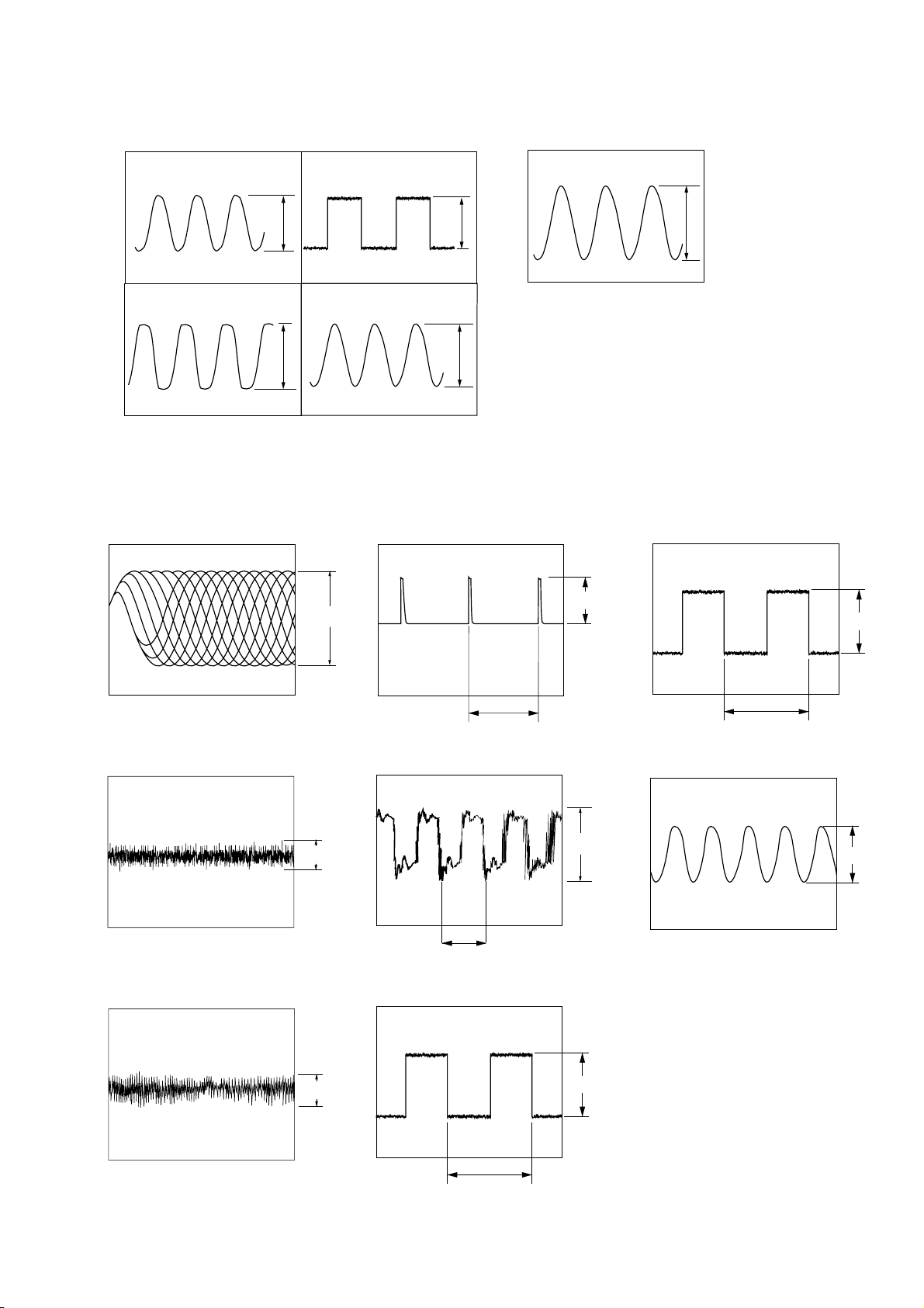
6-23. WAVEFORMS
– MAIN Section – – PANEL Section –
5
1
IC501 0 (X2)
3
IC501 (¡ (CLK-OUT)
IC601 8 (X-OUT)
5.5Vp-p
4.8Vp-p
2
IC501 !£ (XT2)
32.768 kHz
5 MHz
– BD Section –
1 IC101#£ (RFO) (PLAY MODE)
32.768 kHz
4
IC401 #¡ (EXTAL)
10 MHz
1.3 Vp-p
5.0Vp-p
3.6Vp-p
4 IC103@¶ (MDP)
8MHz
2.5 Vp-p
4.2Vp-p
7 IC103&¢ (WFCK)
5 Vp-p
2 IC1012 (FEI) (PLAY MODE)
3 IC101$¶ (TEI) (PLAY MODE)
0.5 Vp-p
0.2 Vp-p
5 IC103^º (XPCK)
230 µs
6 IC103^™ (RFCK)
7.8 µs
5 Vp-p
5 Vp-p
135 µs
8 IC103*ª (XTAI)
2.6 Vp-p
16.9344 MHz
135 µs
— 71 —
Page 50
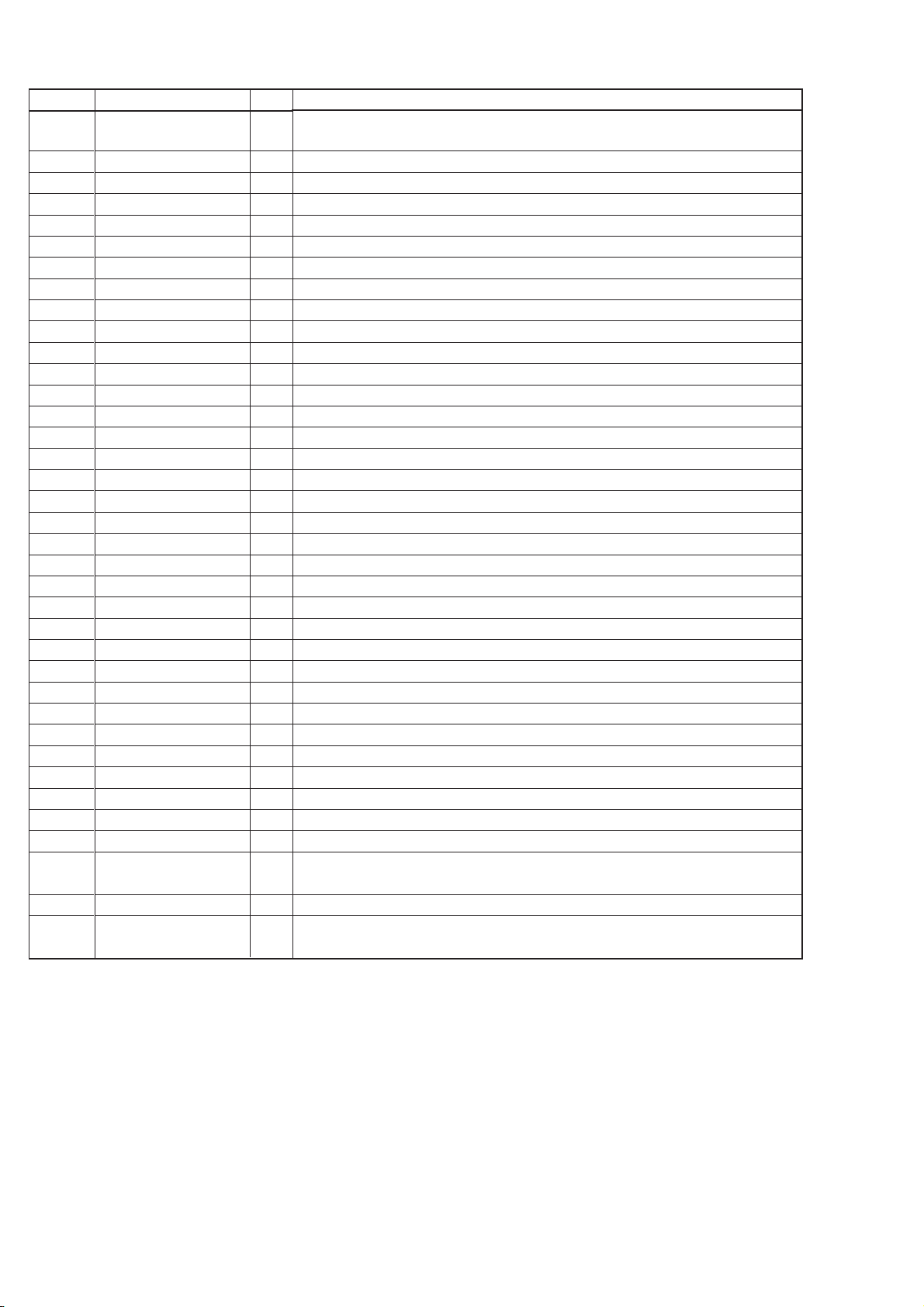
6-24. IC PIN FUNCTION DESCRIPTION
BD BOARD IC101 LA9240M
Pin No. Pin Name I/O Function
1
2
3
4
5
6
7
8
9
10
11
12
13
14
15
16
17
18
19
20
21
22
23
24
25
26
27
28
29
30
31
32
33
34
35
36
37
FIN2
FIN1
E
F
TB
TE–
TE
TESI
SCI
TH
TA
TD–
TD
JP
TO
FD
FD–
FA
FA–
FE
FE–
AGND
SP
SPI
SPG
SP–
SPD
SLEQ
SLD
SL–
SL+
JP–
JP+
TGL
TOFF
TES
HFL
Connected to the pick-up photodiode
I
Added with FIN1 to create RF signal, subtracted with FIN1 to create FE signal
Connected to the pick-up photodiode
I
Connected to the pick-up photodiode Subtracted with F to create TE signal
I
Connected to the pick-up photodiode
I
DC component of the TE signal is input
I
Connects the TE signal gain setting resistor between TE pins
I
TE signal output
O
TES (Track Error Sense) comparator input. The TE signal is band-passed and input
I
Shock detection input
I
Tracking gain time constant setting
I
TA amplifier output
O
Creates a tracking phase compensation constant between TD and VR pins
I
Tracking phase compensation setting
O
Tracking jump signal (kick pulse) amplitude setting
I
Tracking control signal output
O
Focusing control signal output
O
Creates a focusing phase compensation constant between FD and FA pins
I
Creates a focusing phase compensation constant between FD- and FA- pins
O
Creates a focusing phase compensation constant between FA and FE pins
I
FE signal output
O
Connects the FE signal gain setting resistor between TE pins
I
Analog signal Ground
—
Single end output of CV+ and CV- pin signal
O
Spindle amplifier input
I
Gain setting resistor is connected when the spindle 12cm mode
I
Works together with the SPD pin to connect to the spindle phase compensation constant
I
Spindle control signal output
O
Sled phase compensation constant is connected
I
Sled control signal output
O
Sled feeding signal is input from the microprocessor
I
Sled feeding signal is input from the microprocessor
I
Tracking jump signal is input from the DSP
I
Tracking jump signal is input from the DSP
I
Tracking gain control signal is input from the DSP Gain becomes low when TGL is “H”
I
Tracking off control signal is input from the DSP
I
Tracking becomes off when TOFF is “H”
Outputs TES signal to the DSP
O
HFL (High Frequency Level) is used to determine whether the main beam is
O
positioned on a pit or a mirror
— 72 —
Page 51
Pin No.
38
39
40
41
42
43
44
45
46
47
48
49
50
51
52
53
54
55
56
57
58
59
60
61
62
63
64
Pin Name I/O
SLOF
CV–
CV+
RFSM
RFS–
SLC
SLI
DGND
FSC
TBC
NC
DEF
CLK
CL
DA T
CE
DRF
FSS
VCC2
RFFI
VR
LF2
PH1
BH1
LDD
LDS
VCC1
O
O
—
O
—
O
O
—
O
O
—
Function
Sled servo off control input
I
CLV error signal is input from the digital signal processor
I
CLV error signal is input from the digital signal processor
I
RF output
Works together with the RFSM pin to set the RF gain and the 3T compensation constant for
I
the EFM signal
SLI (Slice Level Control) is output to control a data slice level of the RF waveform by the
digital signal processor
Input pin for controlling a data slice level by the digital signal processor
I
Digital Ground
Focus search smoothing capacitor output
TBC (Tracking Balance Control) sets a EF balance variable range
I
Not used
Defect detection output for a disc
Reference clock input The 4.23 MHz of the digital signal processor is input
I
Microprocessor command clock input
I
Microprocessor command data input
I
Microprocessor command chip enable input
I
DRF (Defect RF) outputs a RF level detection
FSS (Focus Search Select) is a switching pin for the focus search mode
I
(±search/+search for a reference voltage)
Servo system and digital system VCC
Reference voltage bus control is connected
I
Reference voltage output
Constant setting for a disc defect detection
I
Connected to the capacitor for the RF signal peak hold
I
Connected to the capacitor for the RF signal bottom hold
I
APC circuit output
APC circuit input
I
RF system VCC
• Abbreviation
EFM : Eight to Fourteen Modulation
APC : Auto Power Control
— 73 —
Page 52
BD BOARD IC102 LC78622E
Pin No. Pin Name I/O Function
1
2
3
4
5
6
7
8
9
10
11
12
13
14
15
16
17
18
19
20
21
22
23
24
25
26
27
28
DEFI
TAI
PDO
VVSS
ISET
VVDD
FR
VSS
EFMO
EFMIN
TEST2
CL V+
CL V–
V/P
HFL
TES
TOFF
TGL
JP+
JP–
PCK
FSEQ
VDD
CONT1
CONT2
CONT3
CONT4
CONT5
I
Defect detection signal (DEF) input (Be sure to connect to 0 when not in use)
I
PLL test input to incorporates a pull-down resistor (Be sure to connect to 0V)
O
PLL phase comparison output for external VCO control
—
PLL ground for the built-in VCO (Be sure to connect to 0 when not in use)
I
Connected to a current adjusting resistor for the PDO output
—
Built-in VCO power supply
I
Adjusts the VCO frequency range
—
Digital Ground to be sure to connect to 0
O
Slice level control to EFM signal output
I
Slice level control to EFM signal input
I
Test input to incorporates a pull-down resistor (Be sure to connect to 0V)
O
Disc motor control output (3-value output available depending on the command)
O
Rough servo/phase control automatic switching monitor output
O
“H”:rough servo, ‘’L”:phase servo
I
Tracking detection signal input (Schmidt input)
I
Tracking error signal input (Schmidt input)
O
Tracking OFF output
O
Tracking gain switching output (Raises gain when “L”)
O
Track jump control output (3-value output available depending on the command)
O
O
EFM data playback clock monitor (4.3218 MHz when phase is locked)
Sync signal detection output (“H” when a sync signal detected from the EFM signal and that
O
generated internally coincide)
—
Digital power supply
General purpose output 1. Performs control using a serial data command from the
microprocessor (When not in use, connect to 0V by setting to an input or set to an open state
I/O
by setting to an output)
General purpose output 2. Performs control using a serial data command from the
microprocessor (When not in use, connect to 0V by setting to an input or set to an open state
I/O
by setting to an output)
General purpose output 3. Performs control using a serial data command from the
microprocessor (When not in use, connect to 0V by setting to an input or set to an open state
I/O
by setting to an output)
General purpose output 4. Performs control using a serial data command from the
microprocessor (When not in use, connect to 0V by setting to an input or set to an open state
I/O
by setting to an output)
General purpose output 5. Performs control using a serial data command from the
microprocessor (When not in use, connect to 0V by setting to an input or set to an open state
I/O
by setting to an output)
• Abbreviation
PLL : Phase Locked Loop
EFM : Eight to Fourteen Modulation
— 74 —
Page 53
Pin No. Pin Name I/O Function
29
30
31
32
33
34
35
36
37
38
39
40
41
42
43
44
45
46
47
48
49
50
51
52
53
54
55
56
57
58
59
60
61
62
63
64
EMPH
C2F
DOUT
TEST3
TEST4
NC
MUTEL
LVDD
LCHO
LVSS
RVSS
RCHO
RVDD
MUTER
XVDD
XOUT
XIN
XVSS
SBSY
EFLG
PW
SFSY
SBCK
FSX
WRQ
RWC
SQOUT
COIN
CQCK
RES
TEST11
16M
4.2M
TEST5
CS
TEST1
O
Deemphasis monitor The deemphasis disc is being played back when “H”
O
C2 flag output
O
Digital OUT output (EIAJ format)
I
Test input Incorporates a pull-down resistor Be sure to connect to 0V
I
Test input Incorporates a pull-down resistor Be sure to connect to 0V
—
Not used Be sure to use it in an open state
O
L channel 1-bit DAC L channel mute output
—
L channel 1-bit DAC L channel power supply
O
L channel 1-bit DAC L channel output
—
L channel 1-bit DAC L channel ground Be sure to connect to 0V
—
R channel 1-bit DAC R channel ground Be sure to connect to 0V
O
R channel 1-bit DAC R channel output
—
R channel 1-bit DAC R channel power supply
O
R channel 1-bit DAC R channel mute output
—
Power supply for the crystal oscillator
O
Connected to the 16.9344 MHz crystal oscillator
I
—
Ground for the crystal oscillator Be sure to connect to 0V
O
Sync signal output for the subcode block
O
C1, C2, single correction, and double correction monitor
O
Subcode P, Q, R, S, T, U, W output
O
Subcode frame sync signal output
Rises when the subcode is in a standby
I
Subcode read clock input Schmidt input (Connect to 0V when not in use)
O
7.35 kHz sync signal output divided from the crystal oscillation
O
Subcode Q output standby output
I
Read/write control input Schmidt input
O
Subcode Q output
I
Command input from the microprocessor
Command input fetching clock input or subcode extracting clock input from SQOUT Schmidt
I
input
I
LC78622 reset input Temporarily set to “L” when the power is turned ON
O
Test output Use it in an open state (Normally, “L” output)
O
16.9344 MHz output
O
4.2336 MHz output
I
Test input. Incorporates a pull-down resistor. Be sure to connect to 0V
Chip select input Incorporates a pull-down resistor
I
Be sure to connect to 0V when not in control
I
Test input Does not incorporates a pull-down resistor Be sure to connect to 0V
Note) Supply the same potential to each power supply pin (VDD, VVDD, LVDD, RVDD, XVDD).
— 75 —
Page 54
MAIN BOARD IC401 CXP84632-031Q
Pin No.
1
2
3
4
5
6 to 13
14 to 28
29
30
31
32
33
34, 35
36
37
38 to 41
42
43 to 46
47
48
49
50
51 to 53
54
55
56
57
58
59
60
61 to 63
64
65
66
67
68
69
70
71
72
73
74
75
76
77
78
79
80
Pin Name
—
ICSW
—
HHOUT
—
D0 to D7
A0 to A14
/WE
RESET
10MHz
10MHz
VSS
—
AVSS
AVREF
—
D-SENS
—
SLED-P
CLK
SUBQ
DATA
—
FOK
WRQ
—
TGL
RWC
SLED-M
—
TSENS1 to TSENS3
DQSY
TCLK
TDATA
TMODE
—
DOORSW
OUTSW
INSW
VDD
—
TBLR
TBLL
LODOUT
LODIN
IICCLK
—
IICDAT
I/O
—
O
—
O
—
I/O
O
O
I
O
I
—
—
—
I
—
I
—
O
O
I
O
—
I
I
—
I
O
O
—
I
I
O
I
O
—
I
I
I
—
—
O
O
O
O
I
—
I/O
Function
Not used
IC reset signal output
Not used
Plus one LED signal output
Not used
SRAM data I/O
SRAM address output
SRAM write enable output
Reset signal input
X’tal(10MHz)
X’tal(10MHz)
Ground
Not used
Analog ground
Analog refernce voltage input
Not used
Disc detect sensor signal input
Not used
Sled motor control signal output
Clock signal output for LC78622E
CD sub-code input from LC78622E
Command output for LC78622E
Not used
DRF(FOK) signal input from LC78622E
Sub-code synchronizing signal input from LC78622E
Not used
Tracking gain control signal input from LC78622E
RWC(latch) output for LC78622E
Sled motor control output
Not used
Table sensor input
Data synchronizing signal input from decoder
Clock output for decoder
Data input from decoder
System down signal output for decoder
Not used
Front cover close detect input
Loading motor out detect input
Loading motor in detect input
Power supply(+5V)
Not used
Table motor counter clock wise turn signal output
Table motor clock wise turn signal output
Loading motor out direction signal output
Loading motor in direction signal output
Serial data clock input
Not used
Serial data I/O
— 76 —
Page 55
MAIN BOARD IC501 uPD780016AYGF-011-3BA
Pin No.
1
2
3
4
5
6
7
8
9
10
11
12
13
14
15
16
17
18
19
20
21
22
23
24
25
26
27
28
29
30
31
32
33
34
35
36
37
38
39
40
41
42
43
44
45
46
47
48
49
50
Pin Name
LINE-MUTE
DBFB-H/L
442-LT
—
POWER
F-RELAY
R-RELAY
PL-RELAY
VSS
X2
X1
VDD
XT2
XT1
RESET
AC-CUT
CAPM-CNT1P
SCOR
SOFT-TEST
CAPM-CNT2P
RDS-INT
RDS-DATA
VDD
AVREF
ADJ
A-SHUT
B-SHUT
B-HALF
—
SPEC-IN
AMS-IN
—
AVSS
SQ-DATA-IN
—
SQ-CLK
SW-ON/OFF
SW-MODE
—
VSS
VOL-LAT
PL-LAT
COM-DIN
COM-DOUT
COM-CLK
CD-POWER
CD-DATA
CD CLK
PL-CLK
PL-DATA
I/O
O
Line mute signal output
O
DBFB H/L select signal output
O
Latch signal output for IC101(M62442FP)
—
Not used
O
Power control signal output
O
Main speaker relay control signal output
O
Surround speaker relay control signal output(Not used)
O
Surround speaker relay control signal output
—
Ground
O
X’tal(5MHz)
I
X’tal(5MHz)
—
Power supply(+5V)
O
X’tal(32.768kHz)
I
X’tal(32.768kHz)
I
Reset signal input
I
AC check input
I
Capstan motor control 1(+) signal output
O
Subcode data request signal output(Not used)
O
Software test port
I
Capstan motor control 2(+) signal output(Not used)
I
Sirial data transfer clock input
I
Serial data input
—
Power supply(+5V)
I
Analog reference voltage input
I
CD adjust point port
I
Deck-A reel pulse detector
I
Deck-B reel pulse detector
I
Half detector signal input
—
Not used
I
Versin select signal input
I
AMS signal input
—
Not used
—
Analog ground
I
Sub code Q data input(Not used)
—
Not used
I
Sub code Q data clock input(Not used)
O
Super woofer ON/OFF control output(Not used)
O
Super woofer mode control output(Not used)
—
Not used
—
Ground
O
Latch signal 2 output for IC201(LV1041M)
O
Latch signal 1 output for IC201(LV1041M)
I
Common serial data input(Not used)
O
Common serial data output(Not used)
O
Common serial clock output(Not used)
O
CD power ON/OFF control output
O
CD data output(Not used)
O
CD clock output(Not used)
O
Clock signal output for IC201(LV1041M)
O
Data signal output for IC201(LV1041M)
Function
— 77 —
Page 56
Pin No. Pin Name I/O Function
51
52
53
54
55
56
57
58
59
60
61
62
63
64
65
66
67
68
69
70
71
72
73
74
75
76
77
78
79
80
81
82
83
84
85
86
87
88
89
90
91
92
93
94
95
96
97
98
99
100
442-CLK
442-DATA
CENTER-MUTE
-
IIC-DATA
IIC-CLK
XRST
XLT
FOCUS-SW
TBL-L
TBL-R
-
LOAD-OUT
LOAD-IN
ST-CLK
ST-DIN
ST-DOUT
ST-CE
TUNED
STEREO
VSS
ST-MUTE
SENS2
SENS
DISC-SENS
T-SENS
CAPM-CNT2P
ENC3
ENC2
ENC1
OUT-OPEN
CAP-M-H/L
B-TRG
A-TRG
CAPM-CNT1M
CAPM-CNT2M
TC-MUTE
R/PB/PAS
NR-ON/OFF
REC-MUTE
CLOCK-OUT
BIAS
EQ-H/N
PB-A/B
A-PLAY-SW
B-PLAY-SW
TC-RELAY
A-HALF
ALC
STK-MUTE
O
Clock signal output for IC101(M62442FP)
O
Data signal output for IC101(M62442FP)
O
Center speaker mute signal output
-
Not used
O
Serial data output
O
Serial data clock output
O
CD reset signal output(Not used)
O
CD latch signal output(Not used)
O
Focus switching signal output(Not used)
O
Table motor control signal output(Not used)
O
Table motor control signal output(Not used)
-
Not used
O
Loading motor control signal output(Not used)
O
Loading motor control signal output(Not used)
O
Tuner clock output
I
Tuner data input
O
Tuner data output
O
Tuner chip enable output
I
Tuned detection for tuner
I
Stereo detection for tuner
-
Ground
O
Tuner mute signal output
I
BD condition signal input(Not used)
I
BD condition signal input(Not used)
I
CD detection signal input(Not used)
I
CD table detection signal input(Not used)
O
Capstan motor control 2(+) signal output(Not used)
I
Disctray address detect encoder input(Not used)
I
Disctray address detect encoder input(Not used)
I
Disctray address detect encoder input(Not used)
I
Out switch signal input(Not used)
O
Capstan motor High/Nomal speed select signal output(Not used)
O
B-deck trigger motor control signal output
O
A-deck trigger motor control signal output
O
Capstan motor control 1(-) signal output
O
Capstan motor control 2(-) signal output
O
TC mute control signal output
I
REC/PB/PASS selection output
O
NR ON/OFF signal output
O
REC mute signal output
O
Clock check output
O
Bias control signal output
O
Equalizer High/Normal control output
O
PB deck A/B select output
I
Deck A play detect input
I
Deck B play detect input
O
Relay control output
I
Deck A cassette detect input
O
ALC control output
O
Power amp mute signal output
— 78 —
Page 57
MAIN BOARD IC601 TMP87CM74AF-6660
Pin No.
1 to 6
7
8
9
10
11,12
13
14 to 18
19,20
21,22
23
24
25
26 to 29
30
31
32
33
34 to 37
38
39
40
41 to 53
54 to 77
78
79,80
Pin Name
LED3 to LED8
VSS
XOUT
XIN
RESET
LED9,LED10
TEST
LED11 to LED15
VOLA,VOLB
JOGA,JOGB
SCL(IIC)
SDA(IIC)
LED SELECT
KEY0 to KEY3
MODEL
LED16
L+R
SIRCS
SPEANA0 to SPEANA3
AVSS
VAREF
VDD
GRID1 to GRID13
SEG1 to SEG24
VKK
LED1,LED2
I/O
O
LED driver output
—
Ground
O
X’tal(5MHz)
I
X’tal(5MHz)
I
Reset signal input
O
LED driver output
—
Not used
O
LED driver output
I
Rotaly encoder pulse input for Volume
I
Rotaly encoder pulse input for Jog
I
Serial data clock input
I
Serial data input
O
LED select signal output
I
Key input
I
Model No. input
O
LED driver output
I
Spectrum analyzer(high frequency)input
I
Remote commander signal input
I
Spectrum analyzer signal input
—
Ground
—
Analog reference voltage input
—
Power supply(+5V)
O
Fluorescent disply tube gride signal output
O
Fluorescent disply tube segment signal output
—
—
O
LED driver output
Function
— 79 —
Page 58
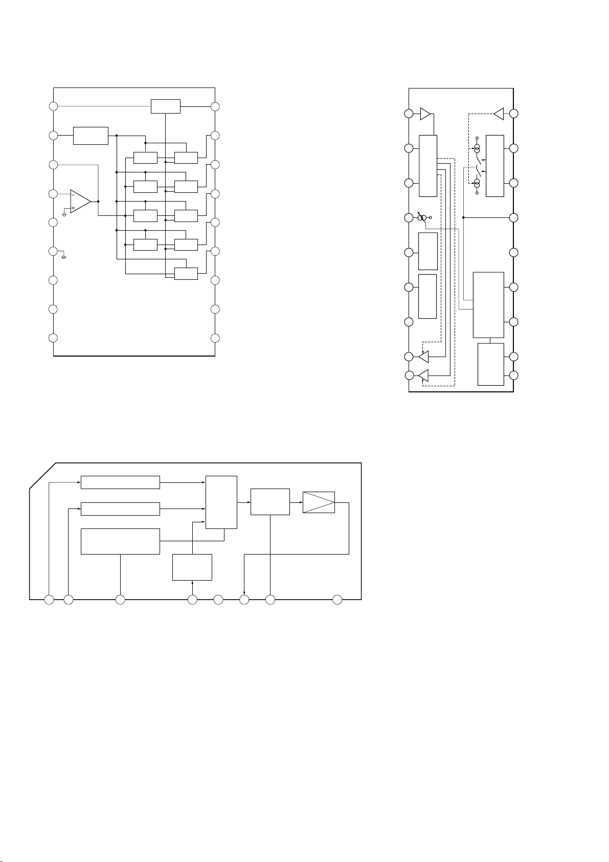
6-25. IC BLOCK DIAGRAMS
RESET
1
C
RESET
IC101 (MAIN BOARD) M62442FPIC603 (PANEL BOARD) BA3833F-E2
18
RESET
VIN1
1
18
VIN2
PREF
LINE
NF
LINE
IN
GND
BIAS
REFFERENCE
2
CURRENT
3
4
5
6
Bias
C
7
NC
8
NC
9
NC
BPF
BPF DET
BPF DET
BPF DET
DET
DET
17
f01
2
FIN1
16
f02
3
RIN1
15
f03
14
f04
13
f
12
VCC
11
NC
10
NC
IOUT
VREF
VREG
VCC
OUT1+
OUT1-
REVERSIBLE DRIVER
4
5
VOLTAGE
REFERENCE
6
LOW VOLTAGE
7
8
+-
9
FWD/REV CONTROLLER
VEE
OUTPUT
OUTPUT
17
16
COVERNER DRIVER
FWD/REV CONTROLLER
VEE VCC
15
14
13
AMPLIFIER
COVERNER
DETECTION
12
LOAD CURRENT
11
OUTPUT
10
COVERNER
FIN2
RIN2
CT2
VEE
FBIN-
FBIN+
OUT2+
OUT2-
IC701 (MAIN BOARD) UPC1237HA
OVER LOAD DET
CC ON
OFFSET DET
LATCH/
AUTORESET
AC OFF
1 2 3 4 5 6 7 8
F/F
DET
V
MUTE
CC
V
— 80 —
Page 59
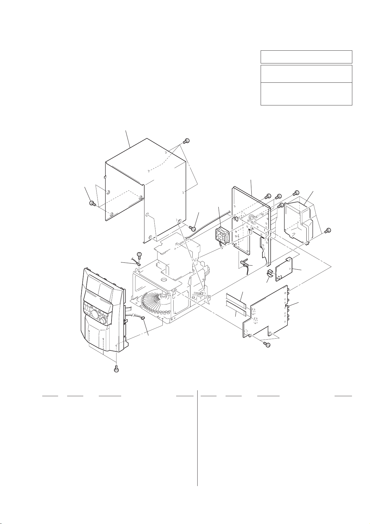
SECTION 7
1
2
#1
1
not suppliednot supplied
#2
not
supplied
#1
#1
8
9
7
5
6
10
FAN101
3
4
#1
#1
#1
#1
#1
EXPLODED VIEWS
NOTE:
• -XX, -X mean standardized parts, so they may
have some differences from the original one.
• Items marked “*” are not stocked since they
are seldom required for routine service. Some
delay should be anticipated when ordering these
items.
• Abbreviation
CND: Canadian
G: German
MY : Malaysia
SP: Singapore
AUS: Australian
7-1. CASE SECTION
• The mechanical parts with no reference number
in the exploded views are not supplied.
• Hardware (# mark) list and accessories and
packing materials are given in the last of this
parts list.
When indicating parts by reference number,
please include the board name.
The components identified by mark ! or
dotted line with mark ! are critical for safety .
Replace only with part number specified.
Les composants identifiés par une marque
! sont critiques pour la sécurité.
Ne les remplacer que par une pièce portant
le numéro spécifié.
Ref. No. Part No. Description Remarks Ref. No. Part No. Description Remarks
1 3-363-099-11 SCREW (CASE 3 TP2)
* 2 4-999-792-01 CASE
* 3 4-999-791-21 PANEL, BACK (FR10:AEP,UK,G)
* 3 4-999-791-41 PANEL, BACK (FR10:AUS)
* 3 4-999-791-51 PANEL, BACK (FR10:SP,MY)
* 3 4-999-791-61 PANEL, BACK (F150:US)
* 3 4-999-791-71 PANEL, BACK (F150:CND)
* 4 4-990-365-11 COVER
5 1-233-544-11 ENCAPSULATED COMPONENT (F150)
5 1-233-546-11 ENCAPSULATED COMPONENT (FR10)
6 1-769-972-11 WIRE(FLAT TYPE)(13 CORE)(F150/FR10:AUS)
* 7 A-4407-776-A MAIN BOARD, COMPLETE (F150:US)
* 7 A-4407-789-A MAIN BOARD, COMPLETE (FR10:AEP,UK,G)
* 7 A-4407-811-A MAIN BOARD, COMPLETE (FR10:SP,MY)
* 7 A-4407-830-A MAIN BOARD, COMPLETE (FR10:AUS)
* 7 A-4414-836-A MAIN BOARD, COMPLETE (F150:CND)
8 1-765-332-11 WIRE (FLAT TYPE) (15 CORE)
9 1-773-055-11 WIRE (FLAT TYPE) (17 CORE)
10 4-956-370-02 BAND, PLUG FIXED (FR10:UK,AUS)
FAN101 1-698-792-11 FAN, DC
6 1-773-004-11 WIRE(FLAT TYPE)(15 CORE)
(FR10:AEP,UK,G,SP,MY)
— 81 —
Page 60
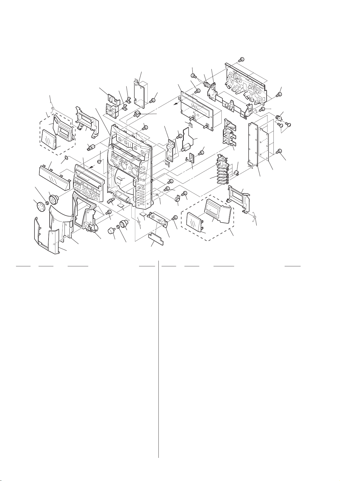
7-2. FRONT PANEL SECTION
#3
not
supplied
56
62
88
57
60
58
75
86
98
59
97
92
99
64
63
53
89
81
52
65
55
66
82
95
54
not
supplied
67
81
95
96
81
61
not supplied
91
80
51
90
68
81
81
79
81
69
81
81
94
72
84
71
81
73
83
87
85
70
77
74
93
76
78
81
81
84
94
81
not supplied
Ref. No. Part No. Description Remarks Ref. No. Part No. Description Remarks
* 51 1-669-681-11 DOOR LED BOARD
52 4-627-936-01 LOCK, MINIATURE SIDE
53 4-973-644-91 KNOB (MIC)(FR10:SP,MY)
54 4-999-653-01 RING (VOL)
55 4-999-655-01 KNOB (VOL)
56 4-999-654-01 KNOB (JOG)
57 4-999-652-01 RING (JOG)
58 4-999-657-01 WINDOW
59 X-4949-856-1 PANEL ASSY, SUB
60 4-999-686-01 SPRING (A DECK)
61 4-999-665-01 BUTTON (KARAOKE)(FR10:SP,MY)
62 X-4949-858-1 HOLDER (L) ASSY, CASSETTE
63 4-999-651-21 PANEL, FRONT (FR10:AUS)
63 4-999-651-31 PANEL, FRONT (FR10:SP,MY)
63 4-999-651-41 PANEL, FRONT (F150:US)
63 4-999-651-51 PANEL, FRONT (F150:CND)
63 4-999-651-61 PANEL, FRONT (FR10:AEP,UK,G)
64 4-999-648-01 BUTTON (POWER)
65 4-999-650-01 INDICATOR (PAUSE)
66 4-999-649-01 INDICATOR (REC)
* 67 1-669-652-11 SW/POWER BOARD
* 68 A-4407-778-A PANEL BOARD, COMPLETE (F150)
* 68 A-4407-791-A PANEL BOARD, COMPLETE (FR10:AEP,UK,G)
* 68 A-4407-824-A PANEL BOARD, COMPLETE (FR10:SP,MY)
* 68 A-4407-832-A PANEL BOARD, COMPLETE (FR10:AUS)
* 72 1-669-650-11 CD DOOR BOARD
73 4-999-645-01 BUTTON (GROUP)
74 4-999-646-01 INDICATOR (G.P)
75 4-999-683-01 RING (MIC) (FR10:SP,MY)
* 76 A-4407-821-A FUNC BOARD, COMPLETE
77 X-4949-859-1 HOLDER (R) ASSY, CASSETTE
78 4-999-687-01 SPRING (B DECK)
79 3-354-963-01 DAMPER
80 4-210-807-01 SPRING (DOOR 2), TORSION
81 4-951-620-01 SCREW (2.6X8), +BVTP
* 82 4-991-854-01 LABEL (DISC)
* 83 4-999-677-01 BRACKET (TC)
84 3-973-975-21 OIL DUMPER
85 4-999-672-01 WINDOW (TC B)
86 4-999-671-01 WINDOW (TC A)
87 X-4949-849-1 LID (A) ASSY, CASSETTE
88 4-999-676-01 LID (B), CASSETTE
89 4-999-681-01 DOOR (REAR)
90 4-999-682-01 INDICATOR (DOOR)
91 4-933-134-61 SCREW (+PTPWH M2.6X6)
92 4-995-728-01 HOLDER (A1), DISC
93 4-995-729-01 HOLDER (A2), DISC
94 4-996-243-01 SCREW (M2), +PSW
95 4-977-358-31 CUSHION
96 4-999-794-01 SPRING (DOOR), TORSION
69 1-769-920-11 WIRE (FLAT TYPE) (9 CORE)
70 4-999-647-01 BUTTON (FUNCTION)
* 71 1-669-648-11 HP/MIC BOARD
97 4-999-680-01 DOOR (CENTER)
98 4-999-679-01 DOOR (FRONT)
99 4-989-312-01 LATCH, NS
— 82 —
Page 61
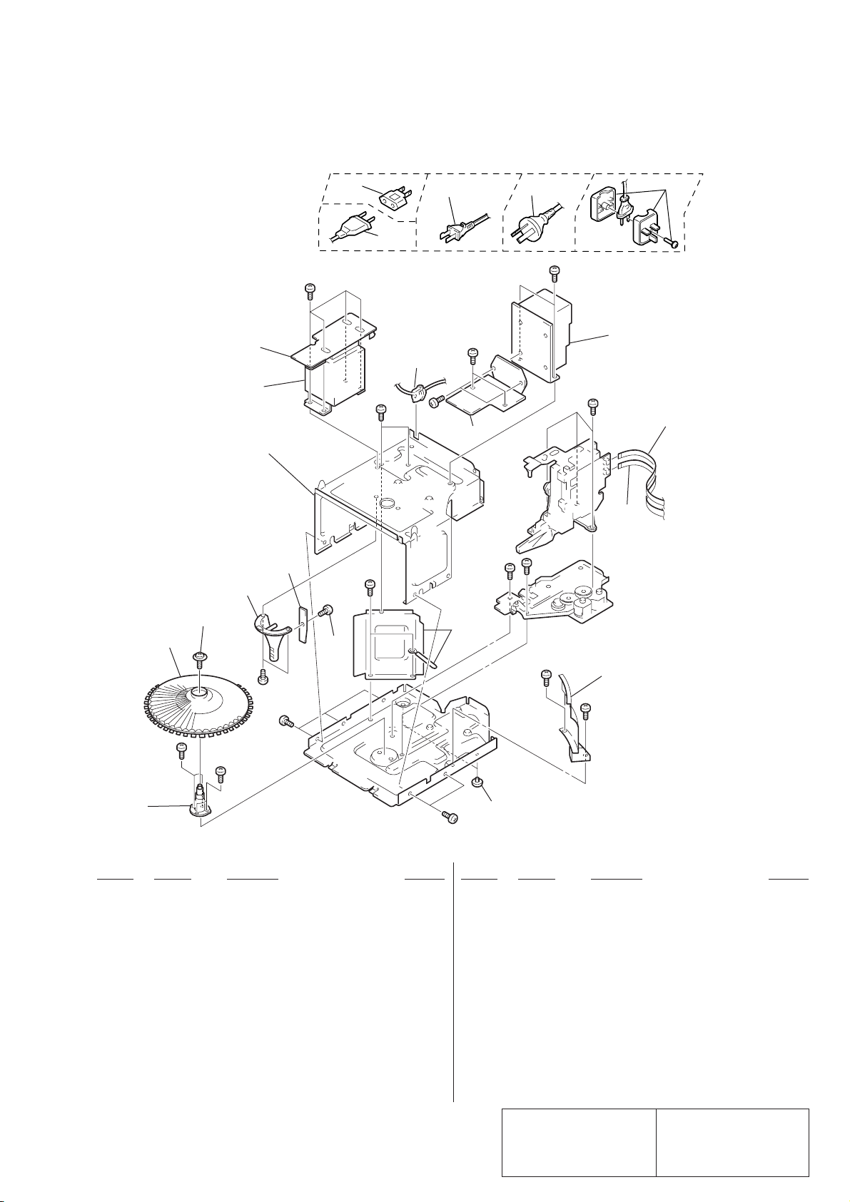
7-3. CHASSIS SECTION
107
T991
not
supplied
104
105
SP,MY MODEL
109
AEP,UK,G,SP,
#2
MY MODEL
#3
#2
114
US, CND MODEL AUS MODEL
114
#2
114
108
#4
115
#6
UK MODEL
109
#2
not supplied
#5
110
111
#5
103
102
#1
#1
#3
#3
106
101
Ref. No. Part No. Description Remarks Ref. No. Part No. Description Remarks
101 4-988-439-01 HOLDER, TABLE
102 4-988-434-01 TABLE (50)
103 4-957-577-31 SCREW PTP WH (2.6X8) (DIA. 10)
* 104 4-990-371-11 HOLDER (LED)
* 105 1-669-645-11 CD LED BOARD
106 4-951-620-01 SCREW (2.6X8), +BVTP
* 107 1-669-649-11 TRANS BOARD
108 3-703-244-00 BUSHING (2104), CORD
! 109 1-569-008-21 ADAPTOR, CONVERSION 2P (SP,MY)
! 109 1-770-019-11 ADAPTOR, CONVERSION PLUG 3P (UK)
not
supplied
#1
112
#1
113
#1
113 4-965-822-01 FOOT
! 114 1-690-609-21 CORD, POWER (US,CND)
! 114 1-696-847-11 CORD, POWER (AUS)
! 114 1-775-787-81 CORD, POWER (AEP,UK,G,SP,MY)
* 115 A-4407-780-A AMP BOARD, COMPLETE (F150:US)
* 115 A-4407-782-A AMP BOARD, COMPLETE (F150:CND)
* 115 A-4407-793-A AMP BOARD, COMPLETE (FR10:AEP,UK,G)
* 115 A-4407-808-A AMP BOARD, COMPLETE (FR10:AUS,SP,MY)
! T991 1-431-842-11 TRANSFORMER, POWER (AUS,SP,MY)
! T991 1-431-843-11 TRANSFORMER, POWER (US)
110 1-782-558-21 WIRE (FLAT TYPE) (16 CORE)
111 1-782-559-21 WIRE (FLAT TYPE) (9 CORE)
* 112 4-990-370-11 COVER (CD)
! T991 1-431-845-11 TRANSFORMER, POWER (AEP,UK,G)
! T991 1-431-844-11 TRANSFORMER, POWER (CND)
— 83 —
The components identified by
mark ! or dotted line with mark
! are critical for safety.
Replace only with part number
specified.
Les composants identifiés par
une marque ! sont critiques
pour la sécurité.
Ne les remplacer que par une
pièce portant le numéro spécifié.
Page 62
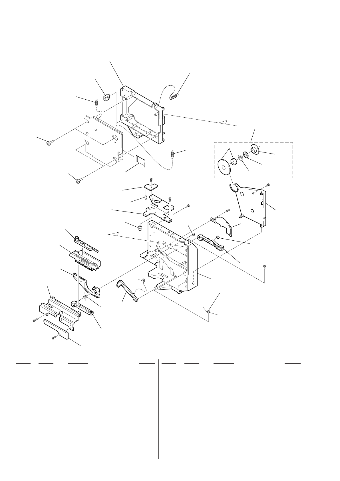
7-4. MECHANISM DECK SECTION-1 (CDM-46B1)
321
327
324
326
324
325
A
316
not supplied
318
#10
302
306
305
326
307
not supplied
A
304
303
323
328
322
319
308
309
#14
#10
#15
313
311
310
#10
not supplied
314
320
312
317
#15
315
#16
#10
301
Ref. No. Part No. Description Remarks Ref. No. Part No. Description Remarks
* 301 1-663-975-11 DOOR SW BOARD
* 302 4-988-427-01 COVER, CAM
303 4-988-420-01 SLIDER (LOADING)
304 4-988-436-01 SPRING (LOADING), TORSION
305 4-988-418-01 HOLDER (A), DISC
* 306 4-988-417-01 SLIDER (CAM)
307 4-988-433-01 SLIDER (LOCK)
308 X-4948-020-1 LEVER (LOADING) ASSY
309 4-988-438-01 SPRING (LEVER), TENSION
310 4-988-437-01 SPRING (HOLDER), TORSION
* 311 4-988-416-01 BASE, LOADING
312 4-988-419-01 HOLDER (B), DISC
313 4-992-069-01 SCREW (+PTPWH) (M2) (DIA. 7)
* 314 4-988-454-01 COVER (LEVER)
* 315 4-988-421-01 HOLDER (MAGNET)
316 A-4672-522-A MAGNET ASSY
317 4-960-633-11 YOKE (MAGNET)
318 4-999-139-01 PULLEY (B)
* 319 4-976-473-01 HOLDER (LED-S)
320 4-988-431-01 ROLLER (DISC)
321 X-4948-019-1 HOLDER ASSY, BU
322 1-777-874-11 WIRE (FLAT TYPE) (16 CORE)
* 323 1-663-973-11 DISC SENSOR (S) BOARD
324 4-988-440-01 SPRING (F-1), TENSION
325 4-988-441-01 SPRING (F-2), TENSION
326 4-957-577-21 SCREW PTP WH (2.6X8) (DIA. 10)
327 4-992-413-02 STOPPER
328 3-910-095-11 RUBBER, VIBRATION PROOF
— 84 —
Page 63
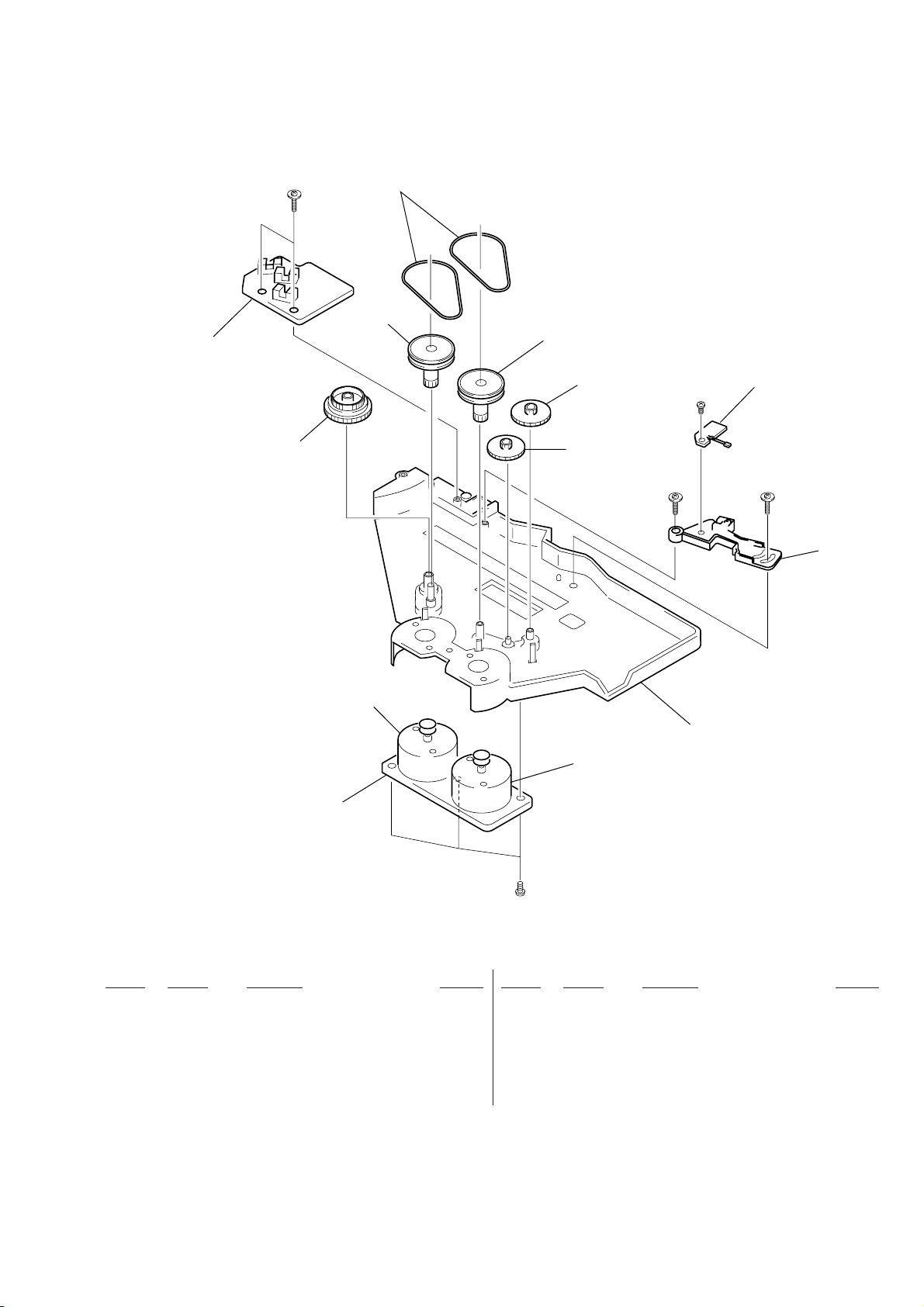
7-5. MECHANISM DECK SECTION-2 (CDM-46B1)
351
352
354
354
353
356
358
360
357
359
355
#1
M61
#20
#17
#14
#17
M62
Ref. No. Part No. Description Remarks Ref. No. Part No. Description Remarks
* 351 1-663-971-11 TABLE SENSOR BOARD
352 4-988-414-01 BELT
353 4-988-423-01 GEAR (A) (LOADING)
354 4-988-425-01 PULLEY
355 4-988-424-01 GEAR (TABLE)
* 357 4-988-426-01 BASE (CDM)
* 358 1-663-972-11 DISC SENSOR (R) BOARD
* 359 1-663-974-01 CD MOTOR BOARD
* 360 4-990-669-01 HOLDER (SENSOR)
M61 X-4948-434-1 MOTOR ASSY (LOADING)
356 4-988-432-01 GEAR (B) (LOADING)
M62 X-4948-434-1 MOTOR ASSY (TABLE)
— 85 —
Page 64
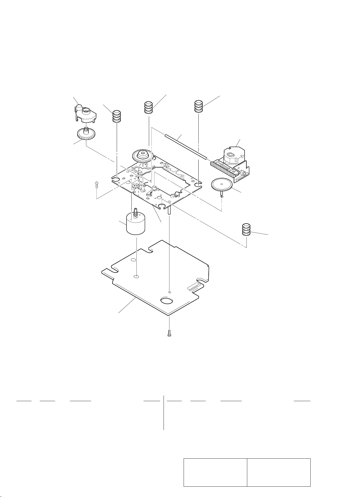
7-6. OPTICAL PICK UP SECTION (KSS-213D/Q-NP)
not supplied
403
#19
406
M102
406
M101
406
404
401
402
406
405
#18
Ref. No. Part No. Description Remarks Ref. No. Part No. Description Remarks
! 401 8-848-379-31 OPTICAL PICK-UP KSS-213D/Q-NP
402 2-626-907-01 GEAR (A) (S)
403 2-627-003-02 GEAR (B) (RP)
404 2-626-908-01 SHAFT, SLED
* 405 A-4699-869-A BD BOARD, COMPLETE
* 406 4-992-054-01 RUBBER, VIBRATION PROOF
M101 X-2646-110-1 T, T CHASSIS ASSY (MG) (F) (SPINDLE)
M102 X-2625-769-1 MOTOR GEAR ASSY (MB) (RP) (SLED)
The components identified by
mark ! or dotted line with mark
! are critical for safety.
Replace only with part number
— 86 —
specified.
Les composants identifiés par
une marque ! sont critiques
pour la sécurité.
Ne les remplacer que par une
pièce portant le numéro spécifié.
Page 65
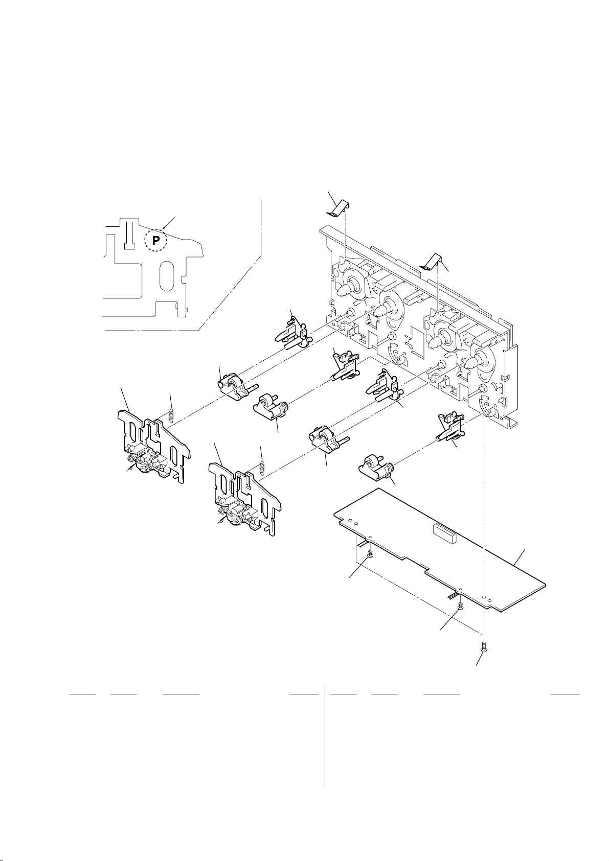
7-7. TAPE MECHANISM DECK SECTION-1
TCM-230AWR1
TCM-230PWR1
*
NOTE: Two types of parts which are not interchangeable are available for the Head deck (A) ASSY and Head
deck (B) ASSY.
When replacing the parts, refer to the following figure, and use the appropriate part
458
Parts with “P” mark: 230PWR1
Parts without “P” mark: 230AWR1
458
457
456
454
HP101
453
HRPE101
453
457
455
456
454
455
459
452
452
451
Ref. No. Part No. Description Remarks Ref. No. Part No. Description Remarks
451 3-376-464-11 SCREW (+PTT 2.6X6), GROUND POINT
452 3-911-116-21 RIVET, PUSH
453 3-016-574-01 SPRING (HEAD),TENSION
454 X-3374-156-2 PINCH LEVER (REV) ASSY
455 X-3374-155-2 PINCH LEVER (FWD) ASSY
456 3-016-564-01 BASE (PINCH LEVER FWD)
457 3-016-565-01 BASE (PINCH LEVER REV)
458 3-016-567-02 SPRING (CASSETTE), LEAF
* 459 A-2007-731-A AUDIO BOARD, COMPLETE
HP101 A-2056-681-A DECK (A) ASSY, HEAD (230AWR1) (*NOTE)
HP101 A-2056-683-A DECK (A) ASSY, HEAD (230PWR1) (*NOTE)
HRPE101A-2056-682-A DECK (B) ASSY, HEAD (230AWR1) (*NOTE)
HRPE101A-2056-684-A DECK (B) ASSY, HEAD (230PWR1) (*NOTE)
— 87 —
Page 66
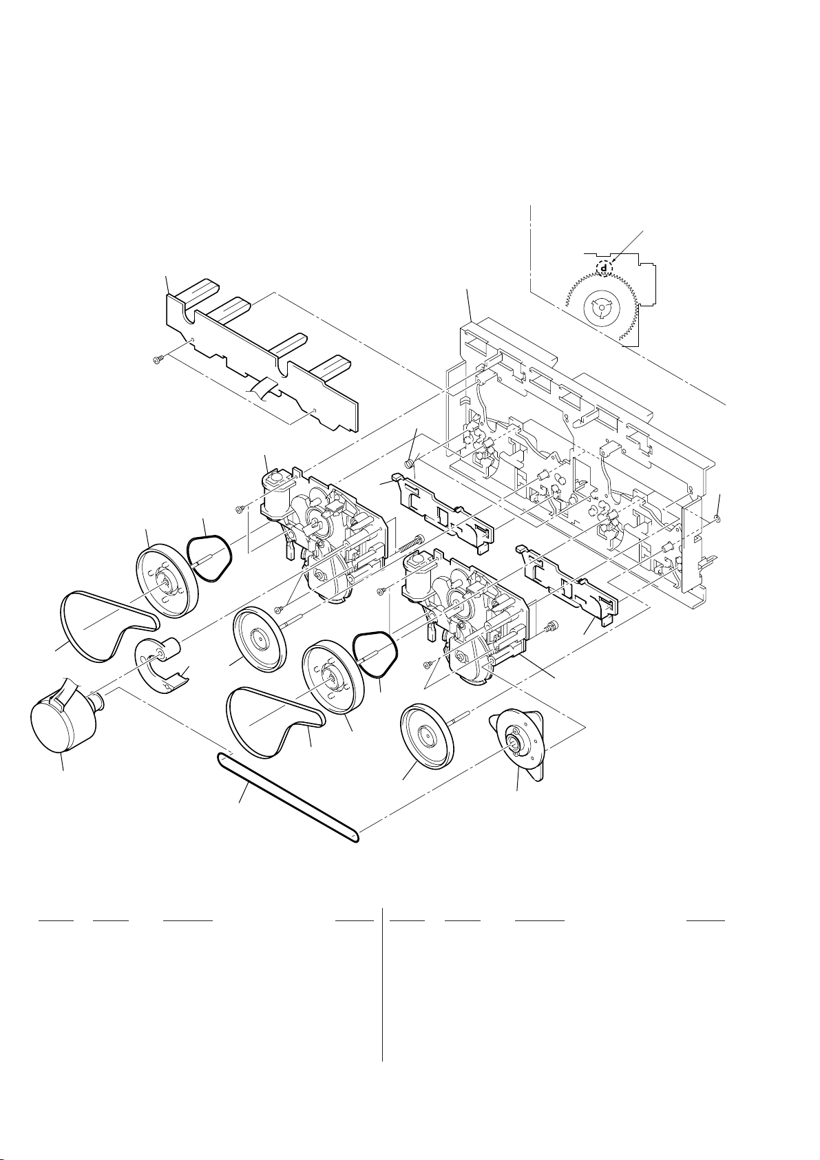
7-8. TAPE MECHANISM DECK SECTION-1
TCM-230AWR1
TCM-230PWR1
*
NOTE: Two types of parts which are not interchangeable are available
for the mechanical block assembly. When replacing the parts,
refer to the following figure, and use the appropriate part.
Parts with “P” mark: 230PWR1
Parts without “P” mark: 230AWR1
502
505
#7
511
508
504
506
#10
509
#10
510
#10
508
512
#12
#10
501
#11
510
509
513
505
502
M1
506
507
503
Ref. No. Part No. Description Remarks Ref. No. Part No. Description Remarks
* 501 X-3374-214-1 CHASSIS ASSY, MAIN
502 3-016-570-01 BELT (CAPSTAN)
503 3-016-569-01 BELT (TENSION)
504 3-017-360-01 BRACKET (MOTOR)
505 X-3374-234-1 FLYWHEEL (FWD) ASSY
506 X-3374-235-1 FLYWHEEL (REV) ASSY
507 X-3374-238-1 PULLEY ASSY, TENSION
508 3-024-405-01 BELT (FR)
509 A-2004-629-A MECHANICAL BLOCK ASSY (230AWR1)
(*NOTE)
509 A-2004-630-A MECHANICAL BLOCK ASSY (230PWR1)
(*NOTE)
510 3-016-566-01 SLIDER, REVERSE
* 511 A-2007-732-A LEAF SW BOARD, COMPLETE
512 3-016-575-01 SPRING, TORSION
513 3-019-208-01 WASHER, STOPPER
M1 A-2004-628-A MOTOR ASSY, CAPSTAN
— 88 —
Page 67
SECTION 8
ELECTRICAL PARTS LIST
AMP
NOTE:
When indicating parts by reference number,
please include the board name.
The components identified by mark ! or
dotted line with mark ! are critical for safety .
Replace only with part number specified.
Les composants identifiés par une marque
! sont critiques pour la sécurité.
Ne les remplacer que par une pièce portant
le numéro spécifié.
• Abbreviation
CND: Canadian
G: German
MY: Malaysia
Ref. No. Part No. Description Remarks Ref. No. Part No. Description Remarks
* A-4407-780-A AMP BOARD, COMPLETE (F150:US)
* A-4407-782-A AMP BOARD, COMPLETE (F150:CND)
* A-4407-793-A AMP BOARD, COMPLETE (FR10:AEP,UK,G)
* A-4407-808-A AMP BOARD, COMPLETE (FR10:AUS,SP,MY)
C801 1-128-582-11 ELECT 10uF 20% 100V
C801 1-126-963-11 ELECT 4.7uF 20% 50V
C802 1-163-007-11 CERAMIC CHIP 680PF 10% 50V
C803 1-163-001-11 CERAMIC CHIP 220PF 10% 50V
C804 1-126-967-11 ELECT 47uF 20% 50V
C806 1-126-967-11 ELECT 47uF 20% 50V
C807 1-128-560-11 ELECT 22uF 20% 100V
C807 1-126-967-11 ELECT 47uF 20% 50V
C809 1-128-560-11 ELECT 22uF 20% 100V
C809 1-126-965-11 ELECT 22uF 20% 50V
C810 1-163-038-91 CERAMIC CHIP 0.1uF 25V
C811 1-136-163-00 FILM 0.068uF 5% 50V
C812 1-136-163-00 FILM 0.068uF 5% 50V
C821 1-106-220-00 MYLAR 0.1uF 5% 100V
C821 1-136-169-00 FILM 0.22uF 5% 50V
SP: Singapore
AUS: Australian
*****************************
******************************
***********************************
************************************
< CAPACITOR >
• Due to standardization, replacements in the
parts list may be different from the parts
specified in the diagrams or the components
used on the set.
• -XX, -X mean standardized parts, so they may
have some difference from the original one.
• Items marked “*” are not stocked since they
are seldom required for routine service. Some
delay should be anticipated when ordering these
items.
• CAPACITORS:
uF: µF
C857 1-126-967-11 ELECT 47uF 20% 50V
C861 1-136-163-00 FILM 0.068uF 5% 50V
C862 1-136-163-00 FILM 0.068uF 5% 50V
C871 1-106-220-00 MYLAR 0.1uF 5% 100V
C871 1-136-169-00 FILM 0.22uF 5% 50V
C872 1-117-750-11 ELECT 3300uF 20% 63V
C872 1-126-974-11 ELECT 3300uF 20% 50V
(F150)
C872 1-125-866-11 ELECT 3300uF 20% 71V
(FR10)
CN803 1-564-511-11 PLUG, CONNECTOR 8P
(F150/FR10:AUS,SP,MY)
(FR10:AEP,UK,G)
(F150/FR10:AUS,SP,MY)
(FR10:AEP,UK,G)
(F150/FR10:AUS,SP,MY)
(FR10:AEP,UK,G)
D801 8-719-988-62 DIODE 1SS355
D811 8-719-988-62 DIODE 1SS355
D812 8-719-988-62 DIODE 1SS355
D813 8-719-988-62 DIODE 1SS355
D821 8-719-510-68 DIODE D5SBA20F01
D851 8-719-988-62 DIODE 1SS355
IC801 8-749-922-65 IC STK-4221MK2 (F150:US)
IC801 8-749-921-04 IC STK-4211MK2 (F150:CND)
IC801 8-749-920-10 IC STK-4172MK2 (FR10:AEP,UK,G)
IC801 8-749-921-68 IC STK-4231MK2 (FR10:AUS,SP,MY)
• RESISTORS
All resistors are in ohms.
METAL: metal-film resistor
METAL OXIDE: Metal Oxide-film resistor
F: nonflammable
• COILS
uH: µH
• SEMICONDUCTORS
In each case, u: µ, for example:
uA...: µA... , uPA... , µPA... ,
uPB... , µPB... , uPC... , µPC... ,
uPD..., µPD...
(FR10:AEP,UK,G)
(F150/FR10:AUS,SP,MY)
(FR10:AEP,UK,G)
(F150)
(FR10:AEP,UK,G)
(FR10:AUS,SP,MY)
< CONNECTOR >
< DIODE >
< IC >
C822 1-117-750-11 ELECT 3300uF 20% 63V
(F150)
C822 1-125-866-11 ELECT 3300uF 20% 71V
(FR10:AUS,SP,MY)
C822 1-126-974-11 ELECT 3300uF 20% 50V
(FR10:AEP,UK,G)
C823 1-126-925-11 ELECT 470uF 20% 10V
C851 1-128-582-11 ELECT 10uF 20% 100V
(F150)
C852 1-163-007-11 CERAMIC CHIP 680PF 10% 50V
C853 1-163-001-11 CERAMIC CHIP 220PF 10% 50V
C854 1-126-967-11 ELECT 47uF 20% 50V
C856 1-126-967-11 ELECT 47uF 20% 50V
C857 1-128-560-11 ELECT 22uF 20% 100V
(F150/FR10:AUS,SP,MY)
< TRANSISTOR >
Q801 8-729-140-84 TRANSISTOR 2SC1841-PAFAEA
Q811 8-729-900-36 TRANSISTOR DTC124ES
Q812 8-729-620-05 TRANSISTOR 2SC2603-EF
Q851 8-729-140-84 TRANSISTOR 2SC1841-PAFAEA
< RESISTOR >
R801 1-216-049-91 RES,CHIP 1K 5% 1/10W
R802 1-216-089-91 RES,CHIP 47K 5% 1/10W
R803 1-216-041-00 METAL CHIP 470 5% 1/10W
(F150/FR10:AUS,SP,MY)
R803 1-216-045-00 METAL CHIP 680 5% 1/10W
(FR10:AEP,UK,G)
R804 1-216-089-91 RES,CHIP 47K 5% 1/10W
— 89 —
Page 68
AMP
Ref. No. Part No. Description Remarks Ref. No. Part No. Description Remarks
R805 1-249-425-11 CARBON 4.7K 5% 1/4W F
R805 1-247-843-11 CARBON 3.3K 5% 1/4W
R806 1-249-425-11 CARBON 4.7K 5% 1/4W F
R806 1-247-843-11 CARBON 3.3K 5% 1/4W
R807 1-212-881-11 FUSIBLE 100 5% 1/4W F
R808 1-220-893-11 METAL 0.22 10% 5W
R808 1-220-755-11 METAL 0.22 10% 2W
R809 1-260-076-11 CARBON 10 5% 1/2W
R811 1-216-049-91 RES,CHIP 1K 5% 1/10W
R812 1-216-077-00 METAL CHIP 15K 5% 1/10W
R813 1-216-097-91 RES,CHIP 100K 5% 1/10W
R815 1-247-843-11 CARBON 3.3K 5% 1/4W
R815 1-249-417-11 CARBON 1K 5% 1/4W F
R816 1-247-843-11 CARBON 3.3K 5% 1/4W
R816 1-249-417-11 CARBON 1K 5% 1/4W F
R821 1-216-069-00 METAL CHIP 6.8K 5% 1/10W
R822 1-216-109-00 METAL CHIP 330K 5% 1/10W
R822 1-216-099-00 METAL CHIP 120K 5% 1/10W
R822 1-216-111-00 METAL CHIP 390K 5% 1/10W
R823 1-216-073-00 METAL CHIP 10K 5% 1/10W
R823 1-216-057-00 METAL CHIP 2.2K 5% 1/10W
R824 1-216-073-00 METAL CHIP 10K 5% 1/10W
R825 1-216-097-91 RES,CHIP 100K 5% 1/10W
R826 1-216-097-91 RES,CHIP 100K 5% 1/10W
R827 1-216-097-91 RES,CHIP 100K 5% 1/10W
R851 1-216-049-91 RES,CHIP 1K 5% 1/10W
R852 1-216-089-91 RES,CHIP 47K 5% 1/10W
R853 1-216-041-00 METAL CHIP 470 5% 1/10W
R853 1-216-045-00 METAL CHIP 680 5% 1/10W
R854 1-216-089-91 RES,CHIP 47K 5% 1/10W
R855 1-249-425-11 CARBON 4.7K 5% 1/4W F
R855 1-247-843-11 CARBON 3.3K 5% 1/4W
R856 1-249-425-11 CARBON 4.7K 5% 1/4W F
R856 1-247-843-11 CARBON 3.3K 5% 1/4W
! R857 1-212-881-11 FUSIBLE 100 5% 1/4W F
! R858 1-220-893-11 METAL 0.22 10% 5W
! R858 1-220-755-11 METAL 0.22 10% 2W
R859 1-260-076-11 CARBON 10 5% 1/2W
R861 1-216-049-91 RES,CHIP 1K 5% 1/10W
AUDIO
(F150/FR10:AUS,SP,MY)
(FR10:AEP,UK,G)
(F150/FR10:AUS,SP,MY)
(FR10:AEP,UK,G)
(F150/FR10:AUS,SP,MY)
(FR10:AEP,UK,G)
(F150/FR10:AUS,SP,MY)
(FR10:AEP,UK,G)
(F150/FR10:AUS,SP,MY)
(FR10:AEP,UK,G)
(F150)
(FR10:AEP,UK,G)
(FR10:AUS,SP,MY)
(F150/FR10:AUS,SP,MY)
(FR10:AEP,UK,G)
(F150/FR10:AUS,SP,MY)
(FR10:AEP,UK,G)
(F150/FR10:AUS,SP,MY)
(FR10:AEP,UK,G)
(F150/FR10:AUS,SP,MY)
(FR10:AEP,UK,G)
(F150/FR10:AUS,SP,MY)
(FR10:AEP,UK,G)
— 90 —
R862 1-216-077-00 METAL CHIP 15K 5% 1/10W
R863 1-216-097-91 RES,CHIP 100K 5% 1/10W
< THERMISTOR >
TH811 1-807-796-11 THERMISTOR
************************************************************
* A-2007-731-A AUDIO BOARD, COMPLETE
**********************
< CAPACITOR >
C301 1-162-289-31 CERAMIC 390PF 10% 50V
C302 1-126-968-11 ELECT 100uF 20% 6.3V
C303 1-162-282-31 CERAMIC 100PF 10% 50V
C304 1-130-483-00 MYLAR 0.01uF 5% 50V
C305 1-107-715-11 ELECT 22uF 20% 16V
C311 1-162-289-31 CERAMIC 390PF 10% 50V
C313 1-162-282-31 CERAMIC 100PF 10% 50V
C314 1-130-487-00 MYLAR 0.022uF 5% 50V
C315 1-126-233-11 ELECT 22uF 20% 50V
C331 1-137-427-11 FILM 120PF 5% 50V
C332 1-162-288-31 CERAMIC 330PF 10% 50V
C333 1-162-209-31 CERAMIC 27PF 5% 50V
C401 1-162-289-31 CERAMIC 390PF 10% 50V
C402 1-126-968-11 ELECT 100uF 20% 6.3V
C403 1-162-282-31 CERAMIC 100PF 10% 50V
C404 1-130-483-00 MYLAR 0.01uF 5% 50V
C405 1-107-715-11 ELECT 22uF 20% 16V
C411 1-162-289-31 CERAMIC 390PF 10% 50V
C413 1-162-282-31 CERAMIC 100PF 10% 50V
C414 1-130-487-00 MYLAR 0.022uF 5% 50V
C415 1-126-233-11 ELECT 22uF 20% 50V
C431 1-137-427-11 FILM 120PF 5% 50V
C432 1-162-288-31 CERAMIC 330PF 10% 50V
C433 1-162-209-31 CERAMIC 27PF 5% 50V
C601 1-104-396-11 ELECT 10uF 20% 16V
C602 1-104-396-11 ELECT 10uF 20% 16V
C611 1-104-396-11 ELECT 10uF 20% 16V
C612 1-104-396-11 ELECT 10uF 20% 16V
C621 1-137-150-11 FILM 0.01uF 5% 100V
C622 1-126-961-11 ELECT 2.2uF 20% 50V
C623 1-136-155-00 FILM 0.015uF 5% 50V
C624 1-130-481-00 MYLAR 0.0068uF 5% 50V
C625 1-130-481-00 MYLAR 0.0068uF 5% 50V
C627 1-124-903-11 ELECT 1uF 20% 50V
C628 1-136-153-00 FILM 0.01uF 5% 50V
C642 1-104-664-11 ELECT 47uF 20% 16V
< CONNECTOR >
CN601 1-568-834-11 SOCKET, CONNECTOR 15P
< IC >
IC601 8-759-111-44 IC UPC4570C-1
IC602 8-759-143-54 IC UPC1330HA
IC611 8-759-111-44 IC UPC4570C-1
The components identified by
mark ! or dotted line with mark
! are critical for safety.
Replace only with part number
specified.
Les composants identifiés par
une marque ! sont critiques
pour la sécurité.
Ne les remplacer que par une
pièce portant le numéro spécifié.
Page 69
AUDIO
Ref. No. Part No. Description Remarks Ref. No. Part No. Description Remarks
< COIL >
L331 1-410-780-11 INDUCTOR 27mH
L431 1-410-780-11 INDUCTOR 27mH
L601 1-414-193-41 INDUCTOR 220uH
L602 1-414-193-41 INDUCTOR 220uH
< TRANSISTOR >
Q621 8-729-142-46 TRANSISTOR 2SC2001-LK
Q622 8-729-142-46 TRANSISTOR 2SC2001-LK
Q623 8-729-801-93 TRANSISTOR 2SD1387
< RESISTOR >
R301 1-247-881-00 CARBON 120K 5% 1/4W
R302 1-249-409-11 CARBON 220 5% 1/4W F
R303 1-249-433-11 CARBON 22K 5% 1/4W
R304 1-247-889-00 CARBON 270K 5% 1/4W
R305 1-247-858-11 CARBON 13K 5% 1/4W
R311 1-247-881-00 CARBON 120K 5% 1/4W
R312 1-247-807-31 CARBON 100 5% 1/4W
R314 1-247-882-11 CARBON 130K 5% 1/4W
R315 1-247-850-11 CARBON 6.2K 5% 1/4W
R331 1-249-430-11 CARBON 12K 5% 1/4W
R401 1-247-881-00 CARBON 120K 5% 1/4W
R402 1-249-409-11 CARBON 220 5% 1/4W F
R403 1-249-433-11 CARBON 22K 5% 1/4W
R404 1-247-889-00 CARBON 270K 5% 1/4W
R405 1-247-858-11 CARBON 13K 5% 1/4W
R411 1-247-881-00 CARBON 120K 5% 1/4W
R412 1-247-807-31 CARBON 100 5% 1/4W
R414 1-247-882-11 CARBON 130K 5% 1/4W
R415 1-247-850-11 CARBON 6.2K 5% 1/4W
R431 1-249-430-11 CARBON 12K 5% 1/4W
R601 1-249-409-11 CARBON 220 5% 1/4W F
R602 1-249-409-11 CARBON 220 5% 1/4W F
R608 1-249-409-11 CARBON 220 5% 1/4W F
R609 1-249-433-11 CARBON 22K 5% 1/4W
R611 1-249-409-11 CARBON 220 5% 1/4W F
R612 1-249-409-11 CARBON 220 5% 1/4W F
R621 1-212-851-00 FUSIBLE 5.6 5% 1/4W F
R622 1-212-851-00 FUSIBLE 5.6 5% 1/4W F
R623 1-249-432-11 CARBON 18K 5% 1/4W
R624 1-249-432-11 CARBON 18K 5% 1/4W
R625 1-249-429-11 CARBON 10K 5% 1/4W
* A-4699-869-A BD BOARD, COMPLETE
*******************
< CAPACITOR >
C101 1-163-038-91 CERAMIC CHIP 0.1uF 25V
C102 1-163-038-91 CERAMIC CHIP 0.1uF 25V
C103 1-164-489-11 CERAMIC CHIP 0.22uF 10% 16V
C104 1-163-003-11 CERAMIC CHIP 330PF 10% 50V
C105 1-163-023-00 CERAMIC CHIP 0.015uF 5% 50V
C106 1-110-501-11 CERAMIC CHIP 0.33uF 10% 16V
C107 1-163-989-11 CERAMIC CHIP 0.033uF 10% 25V
C108 1-164-492-11 CERAMIC CHIP 0.15uF 10% 16V
C109 1-164-161-11 CERAMIC CHIP 0.0022uF 10% 100V
C110 1-163-037-11 CERAMIC CHIP 0.022uF 10% 25V
C111 1-163-989-11 CERAMIC CHIP 0.033uF 10% 25V
C112 1-163-009-11 CERAMIC CHIP 0.001uF 10% 50V
C113 1-164-492-11 CERAMIC CHIP 0.15uF 10% 16V
C114 1-164-492-11 CERAMIC CHIP 0.15uF 10% 16V
C115 1-164-232-11 CERAMIC CHIP 0.01uF 50V
C116 1-164-232-11 CERAMIC CHIP 0.01uF 50V
C117 1-163-001-11 CERAMIC CHIP 220PF 10% 50V
C118 1-107-823-11 CERAMIC CHIP 0.47uF 10% 16V
C119 1-164-489-11 CERAMIC CHIP 0.22uF 10% 16V
C120 1-124-234-00 ELECT 22uF 20% 16V
C121 1-164-182-11 CERAMIC CHIP 0.0033uF 10% 50V
C122 1-126-963-11 ELECT 4.7uF 20% 50V
C123 1-163-038-91 CERAMIC CHIP 0.1uF 25V
C124 1-104-396-11 ELECT 10uF 20% 16V
C125 1-126-177-11 ELECT 100uF 20% 10V
C126 1-126-177-11 ELECT 100uF 20% 10V
C127 1-163-989-11 CERAMIC CHIP 0.033uF 10% 25V
C128 1-163-809-11 CERAMIC CHIP 0.047uF 10% 25V
C129 1-110-501-11 CERAMIC CHIP 0.33uF 10% 16V
C130 1-124-443-00 ELECT 100uF 20% 10V
C131 1-163-009-11 CERAMIC CHIP 0.001uF 10% 50V
C132 1-163-038-91 CERAMIC CHIP 0.1uF 25V
C133 1-163-038-91 CERAMIC CHIP 0.1uF 25V
C141 1-163-038-91 CERAMIC CHIP 0.1uF 25V
C142 1-164-505-11 CERAMIC CHIP 2.2uF 16V
C151 1-107-725-11 CERAMIC CHIP 0.1uF 10% 16V
C152 1-107-725-11 CERAMIC CHIP 0.1uF 10% 16V
C153 1-107-725-11 CERAMIC CHIP 0.1uF 10% 16V
C154 1-163-009-11 CERAMIC CHIP 0.001uF 10% 50V
C155 1-163-093-00 CERAMIC CHIP 10PF 5% 50V
BD
< VARIABLE RESISTOR >
RV301 1-238-598-11 RES, ADJ, CARBON 2.2K
RV311 1-238-598-11 RES, ADJ, CARBON 2.2K
RV341 1-241-768-11 RES, ADJ, CARBON 220K
RV401 1-238-598-11 RES, ADJ, CARBON 2.2K
RV411 1-238-598-11 RES, ADJ, CARBON 2.2K
RV441 1-241-768-11 RES, ADJ, CARBON 220K
< TRANSFORMER >
T621 1-423-980-11 TRANSFORMER, BIAS OSCILLATION
************************************************************
— 91 —
C156 1-163-085-00 CERAMIC CHIP 2PF 50V
C157 1-164-232-11 CERAMIC CHIP 0.01uF 50V
C158 1-163-038-91 CERAMIC CHIP 0.1uF 25V
C159 1-163-101-00 CERAMIC CHIP 22PF 5% 50V
C160 1-163-117-00 CERAMIC CHIP 100PF 5% 50V
C161 1-163-038-91 CERAMIC CHIP 0.1uF 25V
C162 1-163-038-91 CERAMIC CHIP 0.1uF 25V
C163 1-163-038-91 CERAMIC CHIP 0.1uF 25V
C164 1-163-227-11 CERAMIC CHIP 10PF 0.5PF 50V
C165 1-163-227-11 CERAMIC CHIP 10PF 0.5PF 50V
C166 1-124-443-00 ELECT 100uF 20% 10V
C167 1-163-038-91 CERAMIC CHIP 0.1uF 25V
C171 1-163-038-91 CERAMIC CHIP 0.1uF 25V
C172 1-126-177-11 ELECT 100uF 20% 10V
C173 1-124-589-11 ELECT 47uF 20% 16V
Page 70

BD
Ref. No. Part No. Description Remarks Ref. No. Part No. Description Remarks
C174 1-163-038-91 CERAMIC CHIP 0.1uF 25V
C175 1-163-038-91 CERAMIC CHIP 0.1uF 25V
C181 1-104-664-11 ELECT 47uF 20% 16V
C182 1-104-664-11 ELECT 47uF 20% 16V
C183 1-163-003-11 CERAMIC CHIP 330PF 10% 50V
R121 1-216-059-00 METAL CHIP 2.7K 5% 1/10W
R122 1-216-083-00 METAL CHIP 27K 5% 1/10W
R123 1-216-099-00 METAL CHIP 120K 5% 1/10W
R124 1-216-093-00 METAL CHIP 68K 5% 1/10W
R125 1-216-089-91 RES,CHIP 47K 5% 1/10W
C184 1-163-003-11 CERAMIC CHIP 330PF 10% 50V
< CONNECTOR >
CN101 1-770-173-11 CONNECTOR, FFC/FPC 16P
CN102 1-691-894-21 SOCKET, CONNECTOR 16P
* CN103 1-568-852-11 SOCKET, CONNECTOR 9P
< DIODE >
D151 8-719-911-19 DIODE 1SS119
D151 8-719-991-33 DIODE 1SS133T-77
< IC >
IC101 8-759-449-64 IC LA9240M
IC102 8-759-449-65 IC LC78622E
IC103 8-759-449-66 IC LA6541
IC104 8-759-428-57 IC LC89170M
< JUMPER RESISTOR >
JW1 1-216-295-91 SHORT 0
JW2 1-216-295-91 SHORT 0
JW4 1-216-295-91 SHORT 0
JW5 1-216-295-91 SHORT 0
JW6 1-216-295-91 SHORT 0
JW7 1-216-295-91 SHORT 0
JW8 1-216-295-91 SHORT 0
JW9 1-216-295-91 SHORT 0
JW10 1-216-295-91 SHORT 0
< TRANSISTOR >
Q101 8-729-119-78 TRANSISTOR 2SC403SP-51
Q102 8-729-119-78 TRANSISTOR 2SC403SP-51
Q103 8-729-119-76 TRANSISTOR 2SA1175-HFE
< RESISTOR >
R101 1-216-097-91 RES,CHIP 100K 5% 1/10W
R102 1-216-093-00 METAL CHIP 68K 5% 1/10W
R103 1-216-093-00 METAL CHIP 68K 5% 1/10W
R104 1-216-093-00 METAL CHIP 68K 5% 1/10W
R105 1-216-093-00 METAL CHIP 68K 5% 1/10W
R106 1-216-097-91 RES,CHIP 100K 5% 1/10W
R107 1-216-097-91 RES,CHIP 100K 5% 1/10W
R108 1-216-068-00 METAL CHIP 6.2K 5% 1/10W
R109 1-216-076-00 METAL CHIP 13K 5% 1/10W
R110 1-216-093-00 METAL CHIP 68K 5% 1/10W
R111 1-216-057-00 METAL CHIP 2.2K 5% 1/10W
R112 1-216-101-00 METAL CHIP 150K 5% 1/10W
R113 1-216-099-00 METAL CHIP 120K 5% 1/10W
R114 1-216-055-00 METAL CHIP 1.8K 5% 1/10W
R115 1-216-085-00 METAL CHIP 33K 5% 1/10W
R116 1-216-057-00 METAL CHIP 2.2K 5% 1/10W
R117 1-216-085-00 METAL CHIP 33K 5% 1/10W
R118 1-216-081-00 METAL CHIP 22K 5% 1/10W
R119 1-216-064-00 METAL CHIP 4.3K 5% 1/10W
R120 1-216-085-00 METAL CHIP 33K 5% 1/10W
R126 1-216-037-00 METAL CHIP 330 5% 1/10W
R127 1-216-089-91 RES,CHIP 47K 5% 1/10W
R128 1-216-077-00 METAL CHIP 15K 5% 1/10W
R129 1-216-069-00 METAL CHIP 6.8K 5% 1/10W
R130 1-216-113-00 METAL CHIP 470K 5% 1/10W
R131 1-216-113-00 METAL CHIP 470K 5% 1/10W
R132 1-216-065-91 RES,CHIP 4.7K 5% 1/10W
R133 1-216-113-00 METAL CHIP 470K 5% 1/10W
R134 1-216-113-00 METAL CHIP 470K 5% 1/10W
R135 1-216-065-91 RES,CHIP 4.7K 5% 1/10W
R136 1-216-073-00 METAL CHIP 10K 5% 1/10W
R137 1-216-009-00 METAL CHIP 22 5% 1/10W
R138 1-216-089-91 RES,CHIP 47K 5% 1/10W
R141 1-216-083-00 METAL CHIP 27K 5% 1/10W
R151 1-216-045-00 METAL CHIP 680 5% 1/10W
R152 1-216-093-00 METAL CHIP 68K 5% 1/10W
R153 1-216-051-00 METAL CHIP 1.2K 5% 1/10W
R154 1-216-085-00 METAL CHIP 33K 5% 1/10W
R155 1-216-089-91 RES,CHIP 47K 5% 1/10W
R156 1-216-081-00 METAL CHIP 22K 5% 1/10W
R157 1-216-077-00 METAL CHIP 15K 5% 1/10W
R158 1-216-049-91 RES,CHIP 1K 5% 1/10W
R159 1-216-083-00 METAL CHIP 27K 5% 1/10W
R160 1-216-037-00 METAL CHIP 330 5% 1/10W
R161 1-216-073-00 METAL CHIP 10K 5% 1/10W
R162 1-216-037-00 METAL CHIP 330 5% 1/10W
R163 1-216-049-91 RES,CHIP 1K 5% 1/10W
R164 1-216-065-91 RES,CHIP 4.7K 5% 1/10W
R165 1-216-025-91 RES,CHIP 100 5% 1/10W
R166 1-216-025-91 RES,CHIP 100 5% 1/10W
R171 1-216-025-91 RES,CHIP 100 5% 1/10W
R172 1-216-025-91 RES,CHIP 100 5% 1/10W
R173 1-216-025-91 RES,CHIP 100 5% 1/10W
R174 1-216-025-91 RES,CHIP 100 5% 1/10W
R181 1-216-057-00 METAL CHIP 2.2K 5% 1/10W
R182 1-216-057-00 METAL CHIP 2.2K 5% 1/10W
R183 1-216-073-00 METAL CHIP 10K 5% 1/10W
R184 1-216-073-00 METAL CHIP 10K 5% 1/10W
R191 1-216-025-91 RES,CHIP 100 5% 1/10W
R192 1-216-041-00 METAL CHIP 470 5% 1/10W
R193 1-216-041-00 METAL CHIP 470 5% 1/10W
R194 1-216-025-91 RES,CHIP 100 5% 1/10W
R195 1-216-041-00 METAL CHIP 470 5% 1/10W
R196 1-216-025-91 RES,CHIP 100 5% 1/10W
R197 1-216-025-91 RES,CHIP 100 5% 1/10W
< SWITCH >
S101 1-572-085-11 SWITCH, LEAF (LIMIT SW)
< VIBRATOR >
X101 1-577-576-21 VIBRATOR, CRYSTAL 16.93MHz
************************************************************
— 92 —
Page 71
CD DOOR CD LED
CD MOTOR DISC SENSOR (R)
DISC SENSOR (S)
Ref. No. Part No. Description Remarks Ref. No. Part No. Description Remarks
* 1-669-650-11 CD DOOR BOARD
**************
< SWITCH >
S413 1-762-386-11 SWITCH, PUSH
*************************************************************
* 1-669-645-11 CD LED BOARD
*************
< DIODE >
D637 8-719-058-64 DIODE SEL5823A
D638 8-719-058-64 DIODE SEL5823A
D639 8-719-058-03 DIODE SEL5423E
D640 8-719-058-04 DIODE SEL5223S
< RESISTOR >
R653 1-249-402-11 CARBON 56 5% 1/4W F
R654 1-249-402-11 CARBON 56 5% 1/4W F
*************************************************************
* 1-663-974-11 CD MOTOR BOARD
****************
< CONNECTOR >
CN61 1-506-469-11 PIN, CONNECTOR 4P
M61 X-4948-434-1 MOTOR ASSY (LOADING)
M62 X-4948-434-1 MOTOR ASSY (TABLE)
*************************************************************
* 1-663-972-11 DISC SENSOR (R) BOARD
*********************
* 4-990-669-01 HOLDER (SENSOR)
7-685-132-19 SCREW +BTP 2.6X5 TYPE2 N-S
< TRANSISTOR >
Q51 8-729-926-31 PHOTO TRANSISTOR PT483F1S
*************************************************************
* 1-663-973-11 DISC SENSOR (S) BOARD
*********************
* 4-976-473-01 HOLDER (LED-S)
< CONNECTOR >
* CN53 1-568-951-11 PIN, CONNECTOR 2P
< DIODE >
D51 8-719-055-84 DIODE GL-528VS1
< RESISTOR >
R54 1-249-409-11 CARBON 220 5% 1/4W F
*************************************************************
* 1-669-681-11 DOOR LED BOARD
*************************************************************
* 1-663-975-11 DOOR SW BOARD
* CN54 1-568-941-11 PIN, CONNECTOR 3P
*************************************************************
* A-4407-821-A FUNC BOARD, COMPLETE
DOOR LED
D633 8-719-058-03 DIODE SEL5423E
D634 8-719-058-03 DIODE SEL5423E
D635 8-719-058-03 DIODE SEL5423E
D636 8-719-058-03 DIODE SEL5423E
R652 1-249-402-11 CARBON 56 5% 1/4W F
S51 1-571-958-11 SWITCH, PUSH (1 KEY)
S52 1-571-958-11 SWITCH, PUSH (1 KEY)
D619 8-719-058-64 DIODE SEL5823A (CD PLUS ONE)
D620 8-719-058-04 DIODE SEL5223S (1)
D621 8-719-058-04 DIODE SEL5223S (2)
D622 8-719-058-04 DIODE SEL5223S (3)
D623 8-719-058-04 DIODE SEL5223S (4)
D624 8-719-058-04 DIODE SEL5223S (5)
R639 1-216-027-00 METAL CHIP 120 5% 1/10W
R640 1-216-029-00 METAL CHIP 150 5% 1/10W
R641 1-216-029-00 METAL CHIP 150 5% 1/10W
R642 1-216-029-00 METAL CHIP 150 5% 1/10W
R643 1-216-029-00 METAL CHIP 150 5% 1/10W
R644 1-216-029-00 METAL CHIP 150 5% 1/10W
R686 1-216-033-00 METAL CHIP 220 5% 1/10W
R687 1-216-035-00 METAL CHIP 270 5% 1/10W
R688 1-216-039-00 METAL CHIP 390 5% 1/10W
R689 1-216-041-00 METAL CHIP 470 5% 1/10W
R690 1-216-045-00 METAL CHIP 680 5% 1/10W
R691 1-216-047-91 RES,CHIP 820 5% 1/10W
R692 1-216-051-00 METAL CHIP 1.2K 5% 1/10W
R693 1-216-053-00 METAL CHIP 1.5K 5% 1/10W
R694 1-216-057-00 METAL CHIP 2.2K 5% 1/10W
R695 1-216-061-00 METAL CHIP 3.3K 5% 1/10W
R696 1-216-065-91 RES,CHIP 4.7K 5% 1/10W
R697 1-216-069-00 METAL CHIP 6.8K 5% 1/10W
R698 1-216-073-00 METAL CHIP 10K 5% 1/10W
DOOR SW FUNC
***************
< DIODE >
< RESISTOR >
*************
< CONNECTOR >
< SWITCH >
*********************
< DIODE >
< RESISTOR >
— 93 —
Page 72
FUNC
Ref. No. Part No. Description Remarks Ref. No. Part No. Description Remarks
S631 1-762-875-21 SWITCH, KEYBOARD (FUNCTION)
S632 1-762-875-21 SWITCH, KEYBOARD (CONTINUE)
S633 1-762-875-21 SWITCH, KEYBOARD (SHUFFLE)
S634 1-762-875-21 SWITCH, KEYBOARD (PROGRAM)
S635 1-762-875-21 SWITCH, KEYBOARD (REPEAT)
S636 1-762-875-21 SWITCH, KEYBOARD (CD PLUS ONE)
S637 1-762-875-21 SWITCH, KEYBOARD (LOOP)
S638 1-762-875-21 SWITCH, KEYBOARD (FLASH)
S639 1-762-875-21 SWITCH, KEYBOARD (GROUP ENTER)
S640 1-762-875-21 SWITCH, KEYBOARD (1)
S641 1-762-875-21 SWITCH, KEYBOARD (2)
S642 1-762-875-21 SWITCH, KEYBOARD (3)
S643 1-762-875-21 SWITCH, KEYBOARD (4)
S644 1-762-875-21 SWITCH, KEYBOARD (5)
************************************************************
* 1-669-648-11 HP/MIC BOARD
HP/MIC LEAF SW
< SWITCH >
*************
R787 1-216-073-00 METAL CHIP 10K 5% 1/10W
(FR10:SP,MY)
R788 1-216-103-00 METAL CHIP 180K 5% 1/10W
(FR10:SP,MY)
R789 1-216-025-91 RES,CHIP 100 5% 1/10W
(FR10:SP,MY)
< VARIABLE RESISTOR >
RV781 1-225-458-11 RES, VAR, CARBON 50K (FR10:SP,MY)
************************************************************
* A-2007-732-A LEAF SW BOARD, COMPLETE
************************
< CAPACITOR >
C1001 1-124-286-00 ELECT 33uF 20% 10V
< CONNECTOR >
CN1001 1-568-860-11 SOCKET, CONNECTOR 17P
< CAPACITOR >
C781 1-126-964-11 ELECT 10uF 20% 50V
(FR10:SP,MY)
C782 1-163-009-11 CERAMIC CHIP 0.001uF 10% 50V
(FR10:SP,MY)
C783 1-163-243-11 CERAMIC CHIP 47PF 5% 50V
(FR10:SP,MY)
C784 1-163-005-11 CERAMIC CHIP 470PF 10% 50V
(FR10:SP,MY)
C785 1-126-959-11 ELECT 0.47uF 20% 50V
(FR10:SP,MY)
C786 1-163-243-11 CERAMIC CHIP 47PF 5% 50V
(FR10:SP,MY)
C788 1-126-964-11 ELECT 10uF 20% 50V
(FR10:SP,MY)
C789 1-115-339-11 CERAMIC CHIP 0.1uF 10% 50V
(FR10:SP,MY)
C790 1-115-339-11 CERAMIC CHIP 0.1uF 10% 50V
(FR10:SP,MY)
C799 1-126-964-11 ELECT 10uF 20% 50V
(FR10:SP,MY)
< IC >
IC781 8-759-634-50 IC M5218AL (FR10:SP,MY)
< JACK >
J781 1-784-224-11 JACK (LARGE TYPE)(PHONES)
J782 1-784-224-11 JACK (LARGE TYPE)(FR10:SP,MY)
< RESISTOR >
R781 1-216-073-00 METAL CHIP 10K 5% 1/10W
(FR10:SP,MY)
R782 1-216-049-91 RES,CHIP 1K 5% 1/10W
(FR10:SP,MY)
R783 1-216-097-91 RES,CHIP 100K 5% 1/10W
(FR10:SP,MY)
R784 1-216-049-91 RES,CHIP 1K 5% 1/10W
(FR10:SP,MY)
R785 1-216-081-00 METAL CHIP 22K 5% 1/10W
(FR10:SP,MY)
< DIODE >
D1001 8-719-911-19 DIODE 1SS119
D1002 8-719-911-19 DIODE 1SS119
< IC >
IC1001 8-749-014-38 IC PHOTO INTERRUPTER SG-264
IC1002 8-749-014-38 IC PHOTO INTERRUPTER SG-264
< TRANSISTOR >
Q1001 8-729-900-65 TRANSISTOR DTA144ES
< RESISTOR >
R907 1-247-879-11 CARBON 100K 5% 1/4W
R1001 1-249-409-11 CARBON 220 5% 1/4W F
R1002 1-249-409-11 CARBON 220 5% 1/4W F
R1003 1-249-414-11 CARBON 560 5% 1/4W F
R1004 1-247-834-11 CARBON 1.3K 5% 1/4W
R1005 1-247-818-11 CARBON 300 5% 1/4W
R1006 1-247-864-11 CARBON 24K 5% 1/4W
R1007 1-247-856-00 CARBON 11K 5% 1/4W
R1008 1-249-417-11 CARBON 1K 5% 1/4W F
< VARIABLE RESISTOR >
RV1001 1-241-785-11 RES, ADJ, CARBON 10K
RV1002 1-241-785-11 RES, ADJ, CARBON 10K
< SWITCH >
S1001 1-570-953-11 SWITCH, PUSH (1 KEY) (A PLAY)
S1002 1-570-953-11 SWITCH, PUSH (1 KEY) (B PLAY)
S1003 1-771-333-11 SWITCH, LEAF (A HALF)
S1004 1-771-205-11 SWITCH, LEAF (A 120/70)
S1005 1-771-205-11 SWITCH, LEAF (REC A)
S1006 1-771-333-11 SWITCH, LEAF (B HALF)
S1008 1-771-205-11 SWITCH, LEAF (B 120/70)
S1009 1-771-205-11 SWITCH, LEAF (REC B)
************************************************************
— 94 —
Page 73

MAIN
Ref. No. Part No. Description Remarks Ref. No. Part No. Description Remarks
* A-4407-776-A MAIN BOARD, COMPLETE (F150:US)
******************************
* A-4407-789-A MAIN BOARD, COMPLETE (FR10:AEP,UK,G)
************************************
* A-4407-830-A MAIN BOARD, COMPLETE (FR10:AUS)
*******************************
* A-4407-811-A MAIN BOARD, COMPLETE (FR10:SP,MY)
*********************************
* A-4414-836-A MAIN BOARD, COMPLETE (F150:CND)
*******************************
< CAPACITOR >
C195 1-162-306-11 CERAMIC 0.01uF 20% 16V
C196 1-162-306-11 CERAMIC 0.01uF 20% 16V
C301 1-126-960-11 ELECT 1uF 20% 50V
C302 1-130-479-00 MYLAR 0.0047uF 5% 50V
C303 1-136-165-00 FILM 0.1uF 5% 50V
C304 1-136-165-00 FILM 0.1uF 5% 50V
C305 1-126-964-11 ELECT 10uF 20% 50V
C306 1-126-960-11 ELECT 1uF 20% 50V
C307 1-126-959-11 ELECT 0.47uF 20% 50V
C308 1-126-964-11 ELECT 10uF 20% 50V
C101 1-162-286-21 CERAMIC 220PF 10% 50V
C102 1-162-286-21 CERAMIC 220PF 10% 50V
C104 1-126-934-51 ELECT 220UF 50V
C111 1-137-195-11 FILM 0.56uF 5% 50V
C112 1-136-158-00 FILM 0.027uF 5% 50V
C113 1-136-167-00 FILM 0.15uF 5% 50V
C114 1-130-480-00 MYLAR 0.0056uF 5% 50V
C115 1-130-489-00 MYLAR 0.033uF 5% 50V
C116 1-130-473-00 MYLAR 0.0015uF 5% 50V
C117 1-136-153-00 FILM 0.01uF 5% 50V
C118 1-162-288-31 CERAMIC 330PF 10% 50V
C119 1-130-479-00 MYLAR 0.0047uF 5% 50V
C120 1-136-153-00 FILM 0.01uF 5% 50V
C121 1-126-964-11 ELECT 10uF 20% 50V
C122 1-162-291-31 CERAMIC 560PF 10% 50V
C123 1-136-165-00 FILM 0.1uF 5% 50V
C124 1-136-165-00 FILM 0.1uF 5% 50V
C125 1-126-964-11 ELECT 10uF 20% 50V
C131 1-126-967-11 ELECT 47uF 20% 16V
C132 1-126-967-11 ELECT 47uF 20% 16V
C135 1-126-964-11 ELECT 10uF 20% 50V
C136 1-164-159-21 CERAMIC 0.1uF 50V
C141 1-126-959-11 ELECT 0.47uF 20% 50V
C151 1-162-286-21 CERAMIC 220PF 10% 50V
C152 1-162-286-21 CERAMIC 220PF 10% 50V
C161 1-137-195-11 FILM 0.56uF 5% 50V
C162 1-136-158-00 FILM 0.027uF 5% 50V
C163 1-136-167-00 FILM 0.15uF 5% 50V
C164 1-130-480-00 MYLAR 0.0056uF 5% 50V
C165 1-130-489-00 MYLAR 0.033uF 5% 50V
C166 1-130-473-00 MYLAR 0.0015uF 5% 50V
C167 1-136-153-00 FILM 0.01uF 5% 50V
C168 1-162-288-31 CERAMIC 330PF 10% 50V
C169 1-130-479-00 MYLAR 0.0047uF 5% 50V
C170 1-136-153-00 FILM 0.01uF 5% 50V
C171 1-126-964-11 ELECT 10uF 20% 50V
C172 1-162-291-31 CERAMIC 560PF 10% 50V
C173 1-136-165-00 FILM 0.1uF 5% 50V
C174 1-136-165-00 FILM 0.1uF 5% 50V
C175 1-126-964-11 ELECT 10uF 20% 50V
C176 1-136-495-11 FILM 0.068uF 5% 50V
C177 1-136-153-00 FILM 0.01uF 5% 50V
C191 1-126-964-11 ELECT 10uF 20% 50V
C192 1-162-292-31 CERAMIC 680PF 10% 50V
C193 1-126-964-11 ELECT 10uF 20% 50V
C194 1-162-286-21 CERAMIC 220PF 10% 50V
C309 1-136-173-00 FILM 0.47uF 5% 50V
C310 1-162-290-31 CERAMIC 470PF 10% 50V
C311 1-126-964-11 ELECT 10uF 20% 50V
C312 1-126-959-11 ELECT 0.47uF 20% 50V
C313 1-162-294-31 CERAMIC 0.001uF 10% 50V
C314 1-126-964-11 ELECT 10uF 20% 50V
C315 1-126-963-11 ELECT 4.7uF 20% 50V
C316 1-104-665-11 ELECT 100uF 20% 10V
C317 1-104-665-11 ELECT 100uF 20% 10V
C320 1-162-290-31 CERAMIC 470PF 10% 50V
C331 1-164-159-21 CERAMIC 0.1uF 50V
C332 1-164-159-21 CERAMIC 0.1uF 50V
C351 1-126-960-11 ELECT 1uF 20% 50V
C352 1-130-479-00 MYLAR 0.0047uF 5% 50V
C353 1-136-165-00 FILM 0.1uF 5% 50V
C354 1-136-165-00 FILM 0.1uF 5% 50V
C355 1-126-964-11 ELECT 10uF 20% 50V
C356 1-126-960-11 ELECT 1uF 20% 50V
C357 1-126-959-11 ELECT 0.47uF 20% 50V
C358 1-126-964-11 ELECT 10uF 20% 50V
C359 1-136-173-00 FILM 0.47uF 5% 50V
C401 1-104-665-11 ELECT 100uF 20% 10V
C402 1-162-306-11 CERAMIC 0.01uF 20% 16V
C403 1-162-306-11 CERAMIC 0.01uF 20% 16V
C405 1-162-306-11 CERAMIC 0.01uF 20% 16V
C406 1-104-665-11 ELECT 100uF 20% 10V
C410 1-104-665-11 ELECT 100uF 20% 10V
C411 1-110-489-11 CAPACITOR 1F 5.5V
C412 1-164-159-21 CERAMIC 0.1uF 50V
C413 1-162-294-31 CERAMIC 0.001uF 10% 50V
C442 1-126-967-11 ELECT 47uF 20% 50V
(F150/FR10:AEP,UK,G,SP,MY)
C442 1-124-252-00 ELECT 0.33uF 20% 50V
(FR10:AUS)
C443 1-130-477-00 MYLAR 0.0033uF 5% 50V
C444 1-130-477-00 MYLAR 0.0033uF 5% 50V
C451 1-126-934-11 ELECT 220uF 20% 10V
C453 1-164-159-21 CERAMIC 0.1uF 50V
C456 1-164-159-21 CERAMIC 0.1uF 50V
C457 1-164-159-21 CERAMIC 0.1uF 50V
C458 1-164-159-21 CERAMIC 0.1uF 50V
C460 1-164-159-21 CERAMIC 0.1uF 50V
C461 1-126-964-11 ELECT 10uF 20% 50V
C462 1-162-294-31 CERAMIC 0.001uF 10% 50V
C463 1-162-294-31 CERAMIC 0.001uF 10% 50V
C492 1-126-967-11 ELECT 47uF 20% 50V
(F150/FR10:AEP,UK,G,SP,MY)
C492 1-124-252-00 ELECT 0.33uF 20% 50V
(FR10:AUS)
— 95 —
Page 74

MAIN
Ref. No. Part No. Description Remarks Ref. No. Part No. Description Remarks
* CN108 1-568-954-11 PIN, CONNECTOR 5P (F150/FR10:AEP,UK,G)
C493 1-130-477-00 MYLAR 0.0033uF 5% 50V
C494 1-130-477-00 MYLAR 0.0033uF 5% 50V
C501 1-126-967-11 ELECT 47uF 20% 10V
C502 1-164-159-21 CERAMIC 0.1uF 50V
C503 1-136-173-00 FILM 0.47uF 5% 50V
C504 1-126-926-11 ELECT 1000uF 20% 10V
C505 1-162-306-11 CERAMIC 0.01uF 20% 16V
C506 1-136-165-00 FILM 0.1uF 5% 50V
C507 1-164-159-21 CERAMIC 0.1uF 50V
C508 1-104-665-11 ELECT 100uF 20% 10V
C509 1-164-027-11 CERAMIC 22PF 5% 50V
C510 1-164-027-11 CERAMIC 22PF 5% 50V
C511 1-126-934-11 ELECT 220uF 20% 10V
C512 1-164-159-21 CERAMIC 0.1uF 50V
C571 1-109-889-11 ELECT 1uF 20% 50V
C701 1-136-495-11 FILM 0.068uF 5% 50V
C702 1-136-495-11 FILM 0.068uF 5% 50V
C731 1-126-934-11 ELECT 220uF 20% 10V
C732 1-104-665-11 ELECT 100uF 20% 10V
C733 1-126-960-11 ELECT 1uF 20% 50V
C734 1-104-665-11 ELECT 100uF 20% 10V
C751 1-136-495-11 FILM 0.068uF 5% 50V
C752 1-136-495-11 FILM 0.068uF 5% 50V
C756 1-126-963-11 ELECT 4.7uF 20% 50V
C757 1-164-159-21 CERAMIC 0.1uF 50V
C901 1-136-165-00 FILM 0.1uF 5% 50V
C902 1-128-548-11 ELECT 4700uF 20% 25V
C903 1-104-666-11 ELECT 220uF 20% 25V
C904 1-126-967-11 ELECT 47uF 20% 16V
C905 1-126-940-11 ELECT 330uF 20% 16V
C908 1-162-301-11 CERAMIC 0.0015uF 30% 16V
C909 1-126-964-11 ELECT 10uF 20% 50V
C910 1-104-665-11 ELECT 100uF 20% 10V
C911 1-126-964-11 ELECT 10uF 20% 50V
C912 1-126-926-11 ELECT 1000uF 20% 10V
C913 1-126-943-11 ELECT 2200uF 20% 25V
C914 1-126-964-11 ELECT 10uF 20% 50V
C915 1-126-767-11 ELECT 1000uF 20% 16V
C916 1-126-964-11 ELECT 10uF 20% 50V
C917 1-126-767-11 ELECT 1000uF 20% 16V
C918 1-126-968-11 ELECT 100uF 20% 50V
C919 1-126-968-11 ELECT 100uF 20% 50V
C921 1-126-947-11 ELECT 47uF 20% 35V
C922 1-164-159-21 CERAMIC 0.1uF 50V
C923 1-164-159-21 CERAMIC 0.1uF 50V
C924 1-126-934-11 ELECT 220uF 20% 10V
C951 1-136-165-00 FILM 0.1uF 5% 50V
C952 1-126-943-11 ELECT 2200uF 20% 25V
C953 1-104-666-11 ELECT 220uF 20% 25V
C955 1-126-940-11 ELECT 330uF 20% 16V
* CN108 1-568-936-11 PIN, CONNECTOR 9P (FR10:AUS,SP,MY)
* CN110 1-564-506-11 PLUG, CONNECTOR 3P
* CN301 1-568-449-11 HOUSING, CONNECTOR(PC BOARD)3P
CN401 1-784-738-41 CONNECTOR, FFC 16P
CN402 1-784-731-41 CONNECTOR, FFC 9P
* CN403 1-568-951-11 PIN, CONNECTOR 2P
* CN451 1-568-955-11 PIN, CONNECTOR 6P
* CN453 1-568-951-11 PIN, CONNECTOR 2P
CN454 1-506-468-11 PIN, CONNECTOR 3P
CN461 1-506-469-11 PIN, CONNECTOR 4P
CN501 1-784-770-41 CONNECTOR, FFC 9P
< DIODE >
D141 8-719-991-33 DIODE 1SS133T-77
D333 8-719-991-33 DIODE 1SS133T-77
D401 8-719-200-82 DIODE 11ES2
D402 8-719-991-33 DIODE 1SS133T-77
D411 8-719-991-33 DIODE 1SS133T-77
D501 8-719-200-82 DIODE 11ES2
D502 8-719-200-82 DIODE 11ES2
D503 8-719-991-33 DIODE 1SS133T-77
D504 8-719-991-33 DIODE 1SS133T-77
D505 8-719-991-33 DIODE 1SS133T-77
D506 8-719-991-33 DIODE 1SS133T-77
D701 8-719-991-33 DIODE 1SS133T-77
D702 8-719-991-33 DIODE 1SS133T-77
D703 8-719-200-82 DIODE 11ES2
D704 8-719-200-82 DIODE 11ES2
D705 8-719-200-82 DIODE 11ES2
D731 8-719-991-33 DIODE 1SS133T-77
D732 8-719-991-33 DIODE 1SS133T-77
D733 8-719-991-33 DIODE 1SS133T-77
D751 8-719-991-33 DIODE 1SS133T-77
D901 8-719-200-82 DIODE 11ES2
D902 8-719-200-82 DIODE 11ES2
D903 8-719-200-82 DIODE 11ES2
D904 8-719-200-82 DIODE 11ES2
D905 8-719-935-39 DIODE HZS6B1LTD
D906 8-719-991-33 DIODE 1SS133T-77
D907 8-719-200-82 DIODE 11ES2
D908 8-719-200-82 DIODE 11ES2
D909 8-719-200-82 DIODE 11ES2
D910 8-719-200-82 DIODE 11ES2
D911 8-719-934-25 DIODE HZS33-1L
D912 8-719-921-44 DIODE MTZJ-5.1C
D913 8-719-991-33 DIODE 1SS133T-77
D914 8-719-200-82 DIODE 11ES2
D917 8-719-991-33 DIODE 1SS133T-77
< GROUND >
< CONNECTOR >
* CN101 1-564-506-11 PLUG, CONNECTOR 3P
CN102 1-784-774-41 CONNECTOR, FFC 13P (F150)
CN102 1-784-776-41 CONNECTOR, FFC 15P (FR10)
CN106 1-784-776-41 CONNECTOR, FFC 15P
CN107 1-784-778-41 CONNECTOR, FFC 17P
EP401 1-537-771-21 TERMINAL BOARD, GROUND
EP901 1-537-771-21 TERMINAL BOARD, GROUND
< FERRITE BEAD >
FB401 1-412-473-41 INDUCTOR 0UH
FB402 1-412-473-41 INDUCTOR 0UH
FB403 1-412-473-41 INDUCTOR 0UH
FB404 1-412-473-41 INDUCTOR 0UH
FB405 1-412-473-41 INDUCTOR 0UH
— 96 —
Page 75

MAIN
Ref. No. Part No. Description Remarks Ref. No. Part No. Description Remarks
FB406 1-412-473-41 INDUCTOR 0UH
FB407 1-412-473-41 INDUCTOR 0UH
FB408 1-412-473-41 INDUCTOR 0UH
FB409 1-412-473-41 INDUCTOR 0UH
< IC >
IC101 8-759-495-24 IC M62442FP-TP
IC191 8-759-634-51 IC M5218AP
IC301 8-759-495-26 IC HA12215
IC401 8-752-896-35 IC CXP84632-031Q
IC402 8-749-923-04 IC TOTX178
IC411 8-759-463-99 IC M5M5256DFP-70XL (CD DIGITAL)
IC441 8-759-634-51 IC M5218AP
IC461 8-759-356-03 IC BA6780
IC501 8-759-534-06 IC uPD780016AYGF-011-3BA
IC502 8-759-635-63 IC M51943BSL
IC701 8-759-111-68 IC UPC1237HA
IC901 8-759-604-86 IC M5F7807L
IC902 8-759-231-53 IC TA7805S
IC903 8-759-391-87 IC BA78M12P
IC904 8-759-604-38 IC M5F78M10
< JACK >
J101 1-573-028-31 JACK, PIN 4P (VIDEO/MD AUDIO)
J191 1-770-377-31 JACK, PIN 1P (SUPER WOOFER)
Q501 8-729-620-05 TRANSISTOR 2SC2603-EF
Q505 8-729-900-63 TRANSISTOR DTA124ES
Q571 8-729-900-63 TRANSISTOR DTA124ES
Q572 8-729-900-63 TRANSISTOR DTA124ES
Q575 8-729-620-05 TRANSISTOR 2SC2603-EF
Q701 8-729-119-76 TRANSISTOR 2SA1175-HFE
Q702 8-729-620-05 TRANSISTOR 2SC2603-EF
Q703 8-729-119-76 TRANSISTOR 2SA1175-HFE
Q704 8-729-111-29 TRANSISTOR 2SD1616A-K
Q731 8-729-900-63 TRANSISTOR DTA124ES
Q732 8-729-900-63 TRANSISTOR DTA124ES
Q733 8-729-620-05 TRANSISTOR 2SC2603-EF
Q901 8-729-209-15 TRANSISTOR 2SD2012
Q902 8-729-620-05 TRANSISTOR 2SC2603-EF
Q903 8-729-620-05 TRANSISTOR 2SC2603-EF
Q905 8-729-040-20 TRANSISTOR RT1P137L-TP
Q906 8-729-422-57 TRANSISTOR UN4111
Q907 8-729-040-20 TRANSISTOR RT1P137L-TP
Q908 8-729-620-05 TRANSISTOR 2SC2603-EF
Q910 8-729-030-19 TRANSISTOR 2SB1640
Q911 8-729-141-83 TRANSISTOR 2SB1094-LK
Q912 8-729-119-76 TRANSISTOR 2SA1175-HFE
Q913 8-729-620-05 TRANSISTOR 2SC2603-EF
Q914 8-729-620-05 TRANSISTOR 2SC2603-EF
Q915 8-729-620-05 TRANSISTOR 2SC2603-EF
< COIL >
L101 1-408-575-31 INDUCTOR 100uH
L401 1-410-509-11 INDUCTOR 10uH
L402 1-410-509-11 INDUCTOR 10uH
L457 1-410-509-11 INDUCTOR 10uH
L501 1-410-509-11 INDUCTOR 10uH
L701 1-420-872-00 COIL, AIR-CORE
L751 1-420-872-00 COIL, AIR-CORE
< TRANSISTOR >
Q111 8-729-661-90 TRANSISTOR 2SC2603
Q112 8-729-661-90 TRANSISTOR 2SC2603
Q113 8-729-141-31 TRANSISTOR 2SC3623ATP-LK
Q161 8-729-661-90 TRANSISTOR 2SC2603
Q162 8-729-661-90 TRANSISTOR 2SC2603
Q163 8-729-141-31 TRANSISTOR 2SC3623ATP-LK
Q191 8-729-141-31 TRANSISTOR 2SC3623ATP-LK
Q331 8-729-116-57 TRANSISTOR 2SB1068-K
Q332 8-729-900-80 TRANSISTOR DTC114ES
Q333 8-729-116-57 TRANSISTOR 2SB1068-K
Q334 8-729-900-80 TRANSISTOR DTC114ES
Q335 8-729-900-80 TRANSISTOR DTC114ES
Q336 8-729-116-57 TRANSISTOR 2SB1068-K
Q337 8-729-144-44 TRANSISTOR 2SD1513-K
Q338 8-729-900-63 TRANSISTOR DTA124ES
Q339 8-729-900-80 TRANSISTOR DTC114ES
Q340 8-729-116-57 TRANSISTOR 2SB1068-K
Q341 8-729-144-44 TRANSISTOR 2SD1513-K
Q342 8-729-900-63 TRANSISTOR DTA124ES
Q343 8-729-900-80 TRANSISTOR DTC114ES
Q411 8-729-900-36 TRANSISTOR DTC124ES
Q916 8-729-119-76 TRANSISTOR 2SA1175-HFE
Q951 8-729-141-83 TRANSISTOR 2SB1094-LK
Q952 8-729-119-76 TRANSISTOR 2SA1175-HFE
< RESISTOR >
R101 1-249-417-11 CARBON 1K 5% 1/4W F
R102 1-249-417-11 CARBON 1K 5% 1/4W F
R111 1-247-826-00 CARBON 620 5% 1/4W
R112 1-247-903-00 CARBON 1M 5% 1/4W
R113 1-247-903-00 CARBON 1M 5% 1/4W
R114 1-249-419-11 CARBON 1.5K 5% 1/4W F
R115 1-247-863-91 CARBON 22K 5% 1/4W
R116 1-247-887-00 CARBON 220K 5% 1/4W
R117 1-249-429-11 CARBON 10K 5% 1/4W
R118 1-249-437-11 CARBON 47K 5% 1/4W
R119 1-249-421-11 CARBON 2.2K 5% 1/4W F
R120 1-249-441-11 CARBON 100K 5% 1/4W
R121 1-249-429-11 CARBON 10K 5% 1/4W
R123 1-249-437-11 CARBON 47K 5% 1/4W
R124 1-249-421-11 CARBON 2.2K 5% 1/4W F
R125 1-249-429-11 CARBON 10K 5% 1/4W
R128 1-249-421-11 CARBON 2.2K 5% 1/4W F
R131 1-247-807-31 CARBON 100 5% 1/4W
R132 1-247-807-31 CARBON 100 5% 1/4W
R133 1-247-807-31 CARBON 100 5% 1/4W
R141 1-247-863-91 CARBON 22K 5% 1/4W
R142 1-247-863-91 CARBON 22K 5% 1/4W
R143 1-249-417-11 CARBON 1K 5% 1/4W F
(F150/FR10:AUS,SP,MY)
R143 1-249-418-11 CARBON 1.2K 5% 1/4W F
(FR10:AEP,UK,G)
R144 1-249-441-11 CARBON 100K 5% 1/4W
— 97 —
Page 76

MAIN
Ref. No. Part No. Description Remarks Ref. No. Part No. Description Remarks
R145 1-247-903-00 CARBON 1M 5% 1/4W
R151 1-249-417-11 CARBON 1K 5% 1/4W F
R152 1-249-417-11 CARBON 1K 5% 1/4W F
R161 1-247-826-00 CARBON 620 5% 1/4W
R162 1-247-903-00 CARBON 1M 5% 1/4W
R340 1-249-437-11 CARBON 47K 5% 1/4W
R341 1-249-411-11 CARBON 330 5% 1/4W
R342 1-249-437-11 CARBON 47K 5% 1/4W
R343 1-249-417-11 CARBON 1K 5% 1/4W F
R351 1-249-435-11 CARBON 33K 5% 1/4W
R163 1-247-903-00 CARBON 1M 5% 1/4W
R164 1-249-419-11 CARBON 1.5K 5% 1/4W F
R165 1-247-863-91 CARBON 22K 5% 1/4W
R166 1-247-887-00 CARBON 220K 5% 1/4W
R167 1-249-429-11 CARBON 10K 5% 1/4W
R168 1-249-437-11 CARBON 47K 5% 1/4W
R169 1-249-421-11 CARBON 2.2K 5% 1/4W F
R170 1-249-441-11 CARBON 100K 5% 1/4W
R171 1-249-429-11 CARBON 10K 5% 1/4W
R173 1-249-437-11 CARBON 47K 5% 1/4W
R178 1-249-421-11 CARBON 2.2K 5% 1/4W F
R191 1-249-437-11 CARBON 47K 5% 1/4W
R192 1-249-437-11 CARBON 47K 5% 1/4W
R193 1-249-437-11 CARBON 47K 5% 1/4W
R194 1-247-843-11 CARBON 3.3K 5% 1/4W
R195 1-249-429-11 CARBON 10K 5% 1/4W
R196 1-249-417-11 CARBON 1K 5% 1/4W F
R197 1-249-441-11 CARBON 100K 5% 1/4W
R198 1-249-417-11 CARBON 1K 5% 1/4W F
R199 1-249-429-11 CARBON 10K 5% 1/4W
R301 1-249-435-11 CARBON 33K 5% 1/4W
R302 1-249-421-11 CARBON 2.2K 5% 1/4W F
R303 1-247-807-31 CARBON 100 5% 1/4W
R304 1-247-807-31 CARBON 100 5% 1/4W
R305 1-249-421-11 CARBON 2.2K 5% 1/4W F
R306 1-249-428-11 CARBON 8.2K 5% 1/4W F
R307 1-249-428-11 CARBON 8.2K 5% 1/4W F
R308 1-249-425-11 CARBON 4.7K 5% 1/4W F
R309 1-247-863-91 CARBON 22K 5% 1/4W
R311 1-247-903-00 CARBON 1M 5% 1/4W
R312 1-247-883-00 CARBON 150K 5% 1/4W
R313 1-249-441-11 CARBON 100K 5% 1/4W
R315 1-249-429-11 CARBON 10K 5% 1/4W
R316 1-249-432-11 CARBON 18K 5% 1/4W
R317 1-249-429-11 CARBON 10K 5% 1/4W
R318 1-249-429-11 CARBON 10K 5% 1/4W
R319 1-247-893-11 CARBON 390K 5% 1/4W
R321 1-249-422-11 CARBON 2.7K 5% 1/4W F
R322 1-249-428-11 CARBON 8.2K 5% 1/4W F
R324 1-247-876-11 CARBON 75K 5% 1/4W
R325 1-249-437-11 CARBON 47K 5% 1/4W
R326 1-249-437-11 CARBON 47K 5% 1/4W
R327 1-249-437-11 CARBON 47K 5% 1/4W
R328 1-247-876-11 CARBON 75K 5% 1/4W
R329 1-249-417-11 CARBON 1K 5% 1/4W F
R330 1-249-425-11 CARBON 4.7K 5% 1/4W F
R331 1-249-425-11 CARBON 4.7K 5% 1/4W F
R332 1-249-415-11 CARBON 680 5% 1/4W F
R333 1-249-421-11 CARBON 2.2K 5% 1/4W F
R334 1-249-415-11 CARBON 680 5% 1/4W F
R335 1-249-421-11 CARBON 2.2K 5% 1/4W F
R336 1-249-437-11 CARBON 47K 5% 1/4W
R337 1-249-411-11 CARBON 330 5% 1/4W
R338 1-249-411-11 CARBON 330 5% 1/4W
R339 1-249-437-11 CARBON 47K 5% 1/4W
R352 1-249-421-11 CARBON 2.2K 5% 1/4W F
R353 1-247-807-31 CARBON 100 5% 1/4W
R354 1-247-807-31 CARBON 100 5% 1/4W
R355 1-249-421-11 CARBON 2.2K 5% 1/4W F
R356 1-249-428-11 CARBON 8.2K 5% 1/4W F
R357 1-249-428-11 CARBON 8.2K 5% 1/4W F
R358 1-249-425-11 CARBON 4.7K 5% 1/4W F
R359 1-249-435-11 CARBON 33K 5% 1/4W
R401 1-249-437-11 CARBON 47K 5% 1/4W
R405 1-249-429-11 CARBON 10K 5% 1/4W
R411 1-249-437-11 CARBON 47K 5% 1/4W
R412 1-249-437-11 CARBON 47K 5% 1/4W
R414 1-249-429-11 CARBON 10K 5% 1/4W
R415 1-249-435-11 CARBON 33K 5% 1/4W
R416 1-249-437-11 CARBON 47K 5% 1/4W
R417 1-249-437-11 CARBON 47K 5% 1/4W
R418 1-249-437-11 CARBON 47K 5% 1/4W
R419 1-249-425-11 CARBON 4.7K 5% 1/4W F
R433 1-249-437-11 CARBON 47K 5% 1/4W
R434 1-249-437-11 CARBON 47K 5% 1/4W
R441 1-249-419-11 CARBON 1.5K 5% 1/4W F
R442 1-249-429-11 CARBON 10K 5% 1/4W
(F150/FR10:AEP,UK,G,SP,MY)
R442 1-249-435-11 CARBON 33K 5% 1/4W
(FR10:AUS)
R443 1-249-429-11 CARBON 10K 5% 1/4W
R444 1-249-429-11 CARBON 10K 5% 1/4W
R446 1-249-420-11 CARBON 1.8K 5% 1/4W F
R451 1-247-807-31 CARBON 100 5% 1/4W
R461 1-249-382-11 CARBON 1.2 5% 1/6W F
R462 1-249-382-11 CARBON 1.2 5% 1/6W F
R463 1-249-429-11 CARBON 10K 5% 1/4W
R464 1-247-850-11 CARBON 6.2K 5% 1/4W
R465 1-249-429-11 CARBON 10K 5% 1/4W
R466 1-249-428-11 CARBON 8.2K 5% 1/4W F
R491 1-249-419-11 CARBON 1.5K 5% 1/4W F
R492 1-249-429-11 CARBON 10K 5% 1/4W
(F150/FR10:AEP,UK,G,SP,MY)
R492 1-249-435-11 CARBON 33K 5% 1/4W
(FR10:AUS)
R493 1-249-429-11 CARBON 10K 5% 1/4W
R494 1-249-429-11 CARBON 10K 5% 1/4W
R496 1-249-420-11 CARBON 1.8K 5% 1/4W F
R501 1-249-413-11 CARBON 470 5% 1/4W F
R502 1-249-425-11 CARBON 4.7K 5% 1/4W F
R503 1-249-437-11 CARBON 47K 5% 1/4W
R504 1-249-437-11 CARBON 47K 5% 1/4W
R505 1-249-429-11 CARBON 10K 5% 1/4W
R507 1-247-897-11 CARBON 560K 5% 1/4W
R508 1-249-425-11 CARBON 4.7K 5% 1/4W F
R511 1-247-843-11 CARBON 3.3K 5% 1/4W
(FR10:AEP,UK,G)
R511 1-249-425-11 CARBON 4.7K 5% 1/4W F
(FR10:AUS)
R512 1-249-427-11 CARBON 6.8K 5% 1/4W F
(FR10:AEP,UK,G,AUS)
— 98 —
Page 77
MAIN
Ref. No. Part No. Description Remarks Ref. No. Part No. Description Remarks
R522 1-247-807-31 CARBON 100 5% 1/4W
(FR10:AEP,UK,G)
R523 1-247-807-31 CARBON 100 5% 1/4W
(FR10:AEP,UK,G)
R524 1-249-429-11 CARBON 10K 5% 1/4W
R526 1-249-429-11 CARBON 10K 5% 1/4W
R531 1-247-807-31 CARBON 100 5% 1/4W
R736 1-249-425-11 CARBON 4.7K 5% 1/4W F
R737 1-247-791-91 CARBON 22 5% 1/4W
R738 1-249-435-11 CARBON 33K 5% 1/4W
R739 1-249-429-11 CARBON 10K 5% 1/4W
(F150/FR10:AUS,SP,MY)
R739 1-249-427-11 CARBON 6.8K 5% 1/4W F
(FR10:AEP,UK,G)
R532 1-247-807-31 CARBON 100 5% 1/4W
R537 1-249-421-11 CARBON 2.2K 5% 1/4W
R538 1-249-441-11 CARBON 100K 5% 1/4W
R539 1-247-807-31 CARBON 100 5% 1/4W
R540 1-247-807-31 CARBON 100 5% 1/4W
R541 1-247-807-31 CARBON 100 5% 1/4W
R542 1-247-807-31 CARBON 100 5% 1/4W
R543 1-247-807-31 CARBON 100 5% 1/4W
R544 1-249-429-11 CARBON 10K 5% 1/4W
R545 1-247-807-31 CARBON 100 5% 1/4W
R546 1-247-843-11 CARBON 3.3K 5% 1/4W
R547 1-247-807-31 CARBON 100 5% 1/4W
R560 1-249-429-11 CARBON 10K 5% 1/4W
R561 1-247-807-31 CARBON 100 5% 1/4W
R562 1-247-807-31 CARBON 100 5% 1/4W
R563 1-247-807-31 CARBON 100 5% 1/4W
R564 1-247-807-31 CARBON 100 5% 1/4W
R565 1-247-807-31 CARBON 100 5% 1/4W
R566 1-247-807-31 CARBON 100 5% 1/4W
R567 1-247-807-31 CARBON 100 5% 1/4W
R571 1-249-421-11 CARBON 2.2K 5% 1/4W F
R572 1-249-441-11 CARBON 100K 5% 1/4W
R575 1-249-429-11 CARBON 10K 5% 1/4W
R576 1-249-429-11 CARBON 10K 5% 1/4W
R577 1-247-863-91 CARBON 22K 5% 1/4W
R580 1-249-437-11 CARBON 47K 5% 1/4W
R581 1-249-417-11 CARBON 1K 5% 1/4W
R700 1-247-863-91 CARBON 22K 5% 1/4W
R701 1-247-791-91 CARBON 22 5% 1/4W
R702 1-247-791-91 CARBON 22 5% 1/4W
R703 1-247-791-91 CARBON 22 5% 1/4W
R704 1-247-791-91 CARBON 22 5% 1/4W
R705 1-249-437-11 CARBON 47K 5% 1/4W
R706 1-249-437-11 CARBON 47K 5% 1/4W
R707 1-249-429-11 CARBON 10K 5% 1/4W
R708 1-249-429-11 CARBON 10K 5% 1/4W
! R709 1-215-893-11 METAL OXIDE 1.5K 5% 2W F
(F150:US)
! R709 1-216-457-00 METAL OXIDE 1.2K 5% 2W F
(F150:CND)
! R709 1-216-456-00 METAL OXIDE 820 5% 2W F
(FR10:AEP,UK,G)
R740 1-249-429-11 CARBON 10K 5% 1/4W
R741 1-249-429-11 CARBON 10K 5% 1/4W
R742 1-249-429-11 CARBON 10K 5% 1/4W
(F150/FR10:AUS,SP,MY)
R742 1-249-427-11 CARBON 6.8K 5% 1/4W F
(FR10:AEP,UK,G)
R751 1-247-791-91 CARBON 22 5% 1/4W
R752 1-247-791-91 CARBON 22 5% 1/4W
R753 1-247-791-91 CARBON 22 5% 1/4W
R754 1-247-791-91 CARBON 22 5% 1/4W
R755 1-249-437-11 CARBON 47K 5% 1/4W
R756 1-249-425-11 CARBON 4.7K 5% 1/4W F
R757 1-249-441-11 CARBON 100K 5% 1/4W
R758 1-249-421-11 CARBON 2.2K 5% 1/4W F
R776 1-247-807-31 CARBON 100 5% 1/4W
R777 1-247-807-31 CARBON 100 5% 1/4W
R778 1-247-807-31 CARBON 100 5% 1/4W
R779 1-247-807-31 CARBON 100 5% 1/4W
R901 1-247-843-11 CARBON 3.3K 5% 1/4W
R902 1-249-415-11 CARBON 680 5% 1/4W F
R903 1-249-419-11 CARBON 1.5K 5% 1/4W F
R904 1-249-414-11 CARBON 560 5% 1/4W F
R905 1-249-425-11 CARBON 4.7K 5% 1/4W F
R906 1-247-843-11 CARBON 3.3K 5% 1/4W
R907 1-249-415-11 CARBON 680 5% 1/4W F
R908 1-249-429-11 CARBON 10K 5% 1/4W
R909 1-249-430-11 CARBON 12K 5% 1/4W
R910 1-249-429-11 CARBON 10K 5% 1/4W
R912 1-249-425-11 CARBON 4.7K 5% 1/4W F
R913 1-249-429-11 CARBON 10K 5% 1/4W
R914 1-247-815-91 CARBON 220 5% 1/4W
R915 1-247-815-91 CARBON 220 5% 1/4W
R917 1-249-437-11 CARBON 47K 5% 1/4W
R918 1-249-437-11 CARBON 47K 5% 1/4W
R919 1-249-425-11 CARBON 4.7K 5% 1/4W F
R920 1-247-863-91 CARBON 22K 5% 1/4W
R921 1-247-863-91 CARBON 22K 5% 1/4W
R923 1-249-383-11 CARBON 1.5 5% 1/6W F
R924 1-249-383-11 CARBON 1.5 5% 1/6W F
< VARIABLE RESISTOR >
! R709 1-215-892-11 METAL OXIDE 1K 5% 2W F
(FR10:AUS,SP,MY)
R716 1-249-437-11 CARBON 47K 5% 1/4W
R726 1-247-807-31 CARBON 100 5% 1/4W
R727 1-247-807-31 CARBON 100 5% 1/4W
R728 1-247-807-31 CARBON 100 5% 1/4W
R729 1-247-807-31 CARBON 100 5% 1/4W
R731 1-249-438-11 CARBON 56K 5% 1/4W
R732 1-249-437-11 CARBON 47K 5% 1/4W
R734 1-249-429-11 CARBON 10K 5% 1/4W
R735 1-249-425-11 CARBON 4.7K 5% 1/4W F
— 99 —
RV301 1-238-600-11 RES, ADJ, CARBON 10K
RV351 1-238-600-11 RES, ADJ, CARBON 10K
< RELAY >
RY701 1-515-920-11 RELAY (24V)
The components identified by
mark ! or dotted line with mark
! are critical for safety.
Replace only with part number
specified.
Les composants identifiés par
une marque ! sont critiques
pour la sécurité.
Ne les remplacer que par une
pièce portant le numéro spécifié.
Page 78

MAIN
Ref. No. Part No. Description Remarks Ref. No. Part No. Description Remarks
PANEL
< TERMINAL >
< DIODE >
TM701 1-694-055-31 TERMINAL BOARD (SP)
(F150/FR10:AUS,SP,MY)
TM701 1-694-055-41 TERMINAL BOARD (SP) (FR10:AEP,UK,G)
< VIBRATOR >
X401 1-579-175-11 VIBRATOR, CERAMIC 10MHz
X501 1-760-489-11 VIBRATOR, CERAMIC 5MHz
X502 1-567-098-41 VIBRATOR, CRYSTAL 32.768KHz
************************************************************
* A-4407-778-A PANEL BOARD, COMPLETE (F150)
****************************
* A-4407-791-A PANEL BOARD, COMPLETE (FR10:AEP,UK,G)
*************************************
* A-4407-832-A PANEL BOARD, COMPLETE (FR10:AUS)
********************************
* A-4407-824-A PANEL BOARD, COMPLETE (FR10:SP,MY)
**********************************
1-517-773-11 INDICATOR TUBE, FLUORESCENT
* 4-949-935-91 CUSHION (FL)
* 4-990-380-11 HOLDER, FL TUBE
< CAPACITOR >
C601 1-124-584-00 ELECT 100uF 20% 10V
C602 1-165-319-11 CERAMIC CHIP 0.1uF 50V
C603 1-126-157-11 ELECT 10uF 20% 16V
C604 1-165-319-11 CERAMIC CHIP 0.1uF 50V
C605 1-165-319-11 CERAMIC CHIP 0.1uF 50V
C608 1-163-009-11 CERAMIC CHIP 0.001uF 10% 50V
C609 1-124-584-00 ELECT 100uF 20% 10V
C610 1-165-319-11 CERAMIC CHIP 0.1uF 50V
C611 1-163-031-11 CERAMIC CHIP 0.01uF 50V
C612 1-163-031-11 CERAMIC CHIP 0.01uF 50V
C613 1-163-031-11 CERAMIC CHIP 0.01uF 50V
C614 1-163-031-11 CERAMIC CHIP 0.01uF 50V
C615 1-126-160-11 ELECT 1uF 20% 50V
C617 1-126-160-11 ELECT 1uF 20% 50V
C621 1-163-001-11 CERAMIC CHIP 220PF 10% 50V
C622 1-163-001-11 CERAMIC CHIP 220PF 10% 50V
C623 1-163-001-11 CERAMIC CHIP 220PF 10% 50V
C624 1-163-001-11 CERAMIC CHIP 220PF 10% 50V
C625 1-163-001-11 CERAMIC CHIP 220PF 10% 50V
C626 1-163-001-11 CERAMIC CHIP 220PF 10% 50V
D601 8-719-210-33 DIODE EC10DS2
D602 8-719-058-24 DIODE RB501V-40TE-17
D611 8-719-058-64 DIODE SEL5823A (FWD)
D612 8-719-058-64 DIODE SEL5823A (REW)
D613 8-719-058-64 DIODE SEL5823A (GROOVE)
D614 8-719-058-64 DIODE SEL5823A (DSP)
D615 8-719-057-97 DIODE SEL5923A (CD)
D616 8-719-058-04 DIODE SEL5223S (ENTER)
D625 8-719-058-03 DIODE SEL5423E (TAPE A REW)
D626 8-719-058-03 DIODE SEL5423E (TAPE A FWD)
D628 8-719-058-64 DIODE SEL5823A (JOG)
D630 8-719-058-03 DIODE SEL5423E (TAPE B REW)
D631 8-719-058-03 DIODE SEL5423E (TAPE B FWD)
D632 8-719-058-03 DIODE SEL5423E (CD)
< FERRITE BEAD >
FB601 1-500-451-11 FERRITE 0UH
FB602 1-500-451-11 FERRITE 0UH
FB603 1-500-451-11 FERRITE 0UH
< IC >
IC601 8-759-537-37 IC TMP87CM74AF-6660
IC602 8-749-011-05 IC GP1U28X
IC603 8-759-495-25 IC BA3833F-E2
< COIL >
L601 1-408-777-00 INDUCTOR CHIP 10uH
L602 1-408-777-00 INDUCTOR CHIP 10uH
< TRANSISTOR >
Q601 8-729-620-05 TRANSISTOR 2SC2603-EF
Q602 8-729-119-76 TRANSISTOR 2SA1175-HFE
Q603 8-729-119-76 TRANSISTOR 2SA1175-HFE
Q604 8-729-900-36 TRANSISTOR DTC124ES
Q605 8-729-900-36 TRANSISTOR DTC124ES
Q608 8-729-900-36 TRANSISTOR DTC124ES
Q609 8-729-900-36 TRANSISTOR DTC124ES
Q611 8-729-119-76 TRANSISTOR 2SA1175-HFE
Q612 8-729-119-76 TRANSISTOR 2SA1175-HFE
Q621 8-729-620-05 TRANSISTOR 2SC2603-EF
< RESISTOR >
C627 1-163-001-11 CERAMIC CHIP 220PF 10% 50V
C628 1-163-001-11 CERAMIC CHIP 220PF 10% 50V
C629 1-163-001-11 CERAMIC CHIP 220PF 10% 50V
C630 1-163-001-11 CERAMIC CHIP 220PF 10% 50V
C631 1-163-001-11 CERAMIC CHIP 220PF 10% 50V
C632 1-163-001-11 CERAMIC CHIP 220PF 10% 50V
C633 1-163-001-11 CERAMIC CHIP 220PF 10% 50V
C641 1-164-182-11 CERAMIC CHIP 0.0033uF 10% 50V
C642 1-126-157-11 ELECT 10uF 20% 16V
C643 1-126-157-11 ELECT 10uF 20% 16V
C644 1-124-584-00 ELECT 100uF 20% 10V
C645 1-165-319-11 CERAMIC CHIP 0.1uF 50V
C651 1-163-031-11 CERAMIC CHIP 0.01uF 50V
C652 1-163-031-11 CERAMIC CHIP 0.01uF 50V
R601 1-216-061-00 METAL CHIP 3.3K 5% 1/10W
R602 1-216-073-00 METAL CHIP 10K 5% 1/10W
R603 1-216-121-91 RES,CHIP 1M 5% 1/10W
R604 1-216-085-00 METAL CHIP 33K 5% 1/10W
R605 1-216-085-00 METAL CHIP 33K 5% 1/10W
R606 1-216-085-00 METAL CHIP 33K 5% 1/10W
R607 1-216-073-00 METAL CHIP 10K 5% 1/10W
R608 1-216-073-00 METAL CHIP 10K 5% 1/10W
R609 1-216-073-00 METAL CHIP 10K 5% 1/10W
R610 1-216-073-00 METAL CHIP 10K 5% 1/10W
R611 1-216-061-00 METAL CHIP 3.3K 5% 1/10W
R612 1-216-061-00 METAL CHIP 3.3K 5% 1/10W
R613 1-216-025-91 RES,CHIP 100 5% 1/10W
R614 1-216-017-91 RES,CHIP 47 5% 1/10W
R615 1-216-009-00 METAL CHIP 22 5% 1/10W
— 100 —
Page 79
PANEL
Ref. No. Part No. Description Remarks Ref. No. Part No. Description Remarks
R616 1-216-009-00 METAL CHIP 22 5% 1/10W
R617 1-216-081-00 METAL CHIP 22K 5% 1/10W
R618 1-216-107-00 METAL CHIP 270K 5% 1/10W
R619 1-216-097-91 RES,CHIP 100K 5% 1/10W
R620 1-216-089-91 RES,CHIP 47K 5% 1/10W
S606 1-762-875-21 SWITCH, KEYBOARD (TIMER SELECT)
S607 1-762-875-21 SWITCH, KEYBOARD (MEMO SEARCH)
S608 1-762-875-21 SWITCH, KEYBOARD (MEMO SCAN)
S609 1-762-875-21 SWITCH, KEYBOARD (MEMO INPUT)
S610 1-762-875-21 SWITCH, KEYBOARD (CHECK)
SW/POWERPON
R621 1-216-061-00 METAL CHIP 3.3K 5% 1/10W
R622 1-216-061-00 METAL CHIP 3.3K 5% 1/10W
R623 1-216-073-00 METAL CHIP 10K 5% 1/10W
R624 1-216-097-91 RES,CHIP 100K 5% 1/10W
R625 1-216-089-91 RES,CHIP 47K 5% 1/10W
R626 1-216-033-00 METAL CHIP 220 5% 1/10W
R627 1-216-089-91 RES,CHIP 47K 5% 1/10W
R628 1-216-033-00 METAL CHIP 220 5% 1/10W
R629 1-216-099-00 METAL CHIP 120K 5% 1/10W
R633 1-216-027-00 METAL CHIP 120 5% 1/10W
R634 1-216-027-00 METAL CHIP 120 5% 1/10W
R635 1-216-027-00 METAL CHIP 120 5% 1/10W
R636 1-216-027-00 METAL CHIP 120 5% 1/10W
R637 1-216-025-91 RES,CHIP 100 5% 1/10W
R638 1-216-029-00 METAL CHIP 150 5% 1/10W
R645 1-216-033-00 METAL CHIP 220 5% 1/10W
R646 1-216-033-00 METAL CHIP 220 5% 1/10W
R648 1-216-033-00 METAL CHIP 220 5% 1/10W
R649 1-216-033-00 METAL CHIP 220 5% 1/10W
R650 1-216-033-00 METAL CHIP 220 5% 1/10W
R651 1-216-033-00 METAL CHIP 220 5% 1/10W
R655 1-216-069-00 METAL CHIP 6.8K 5% 1/10W
R661 1-216-069-00 METAL CHIP 6.8K 5% 1/10W
R662 1-216-033-00 METAL CHIP 220 5% 1/10W
R663 1-216-035-00 METAL CHIP 270 5% 1/10W
S611 1-762-875-21 SWITCH, KEYBOARD (CLEAR)
S612 1-762-875-21 SWITCH, KEYBOARD (DELETE)
S613 1-762-875-21 SWITCH, KEYBOARD (REW)
S614 1-762-875-21 SWITCH, KEYBOARD (FILE SELECT)
S615 1-762-875-21 SWITCH, KEYBOARD (ENTER)
S616 1-762-875-21 SWITCH, KEYBOARD (FWD)
S617 1-762-875-21 SWITCH, KEYBOARD (TAPE B REW)
S618 1-762-875-21 SWITCH, KEYBOARD (TAPE B FWD)
S619 1-762-875-21 SWITCH, KEYBOARD (CD)
S620 1-762-875-21 SWITCH, KEYBOARD (GROOVE)
S621 1-762-875-21 SWITCH, KEYBOARD (DBFB)
S622 1-762-875-21 SWITCH, KEYBOARD (DSP)
S623 1-762-875-21 SWITCH, KEYBOARD (STOP)
S651 1-473-392-31 ENCODER, ROTARY (VOLUME)
S652 1-473-393-31 ENCODER, ROTARY (JOG)
< VIBRATOR >
X601 1-579-952-21 VIBRATOR, CERAMIC 8MHz
************************************************************
* 1-669-654-11 PON BOARD (FR10:SP,MY)
**********************
< RESISTOR >
R660 1-216-045-00 METAL CHIP 680 5% 1/10W
R664 1-216-039-00 METAL CHIP 390 5% 1/10W
R665 1-216-041-00 METAL CHIP 470 5% 1/10W
R666 1-216-045-00 METAL CHIP 680 5% 1/10W
R667 1-216-047-91 RES,CHIP 820 5% 1/10W
R668 1-216-051-00 METAL CHIP 1.2K 5% 1/10W
R669 1-216-053-00 METAL CHIP 1.5K 5% 1/10W
R670 1-216-057-00 METAL CHIP 2.2K 5% 1/10W
R671 1-216-061-00 METAL CHIP 3.3K 5% 1/10W
R672 1-216-065-91 RES,CHIP 4.7K 5% 1/10W
R673 1-216-069-00 METAL CHIP 6.8K 5% 1/10W
R674 1-216-073-00 METAL CHIP 10K 5% 1/10W
R675 1-216-079-00 METAL CHIP 18K 5% 1/10W
R676 1-216-689-11 METAL CHIP 39K 0.5% 1/10W
R677 1-216-069-00 METAL CHIP 6.8K 5% 1/10W
R678 1-216-033-00 METAL CHIP 220 5% 1/10W
R679 1-216-035-00 METAL CHIP 270 5% 1/10W
R680 1-216-039-00 METAL CHIP 390 5% 1/10W
R681 1-216-041-00 METAL CHIP 470 5% 1/10W
R682 1-216-045-00 METAL CHIP 680 5% 1/10W
R683 1-216-047-91 RES,CHIP 820 5% 1/10W
R685 1-216-069-00 METAL CHIP 6.8K 5% 1/10W
< SWITCH >
S601 1-762-875-21 SWITCH, KEYBOARD (TAPE A FWD)
S602 1-762-875-21 SWITCH, KEYBOARD (TAPE A REW)
S603 1-762-875-21 SWITCH, KEYBOARD (TUNER/BAND)
S604 1-762-875-21 SWITCH, KEYBOARD (DISPLAY/DEMO)
S605 1-762-875-21 SWITCH, KEYBOARD (CLOCK TIMER)
< SWITCH >
S630 1-762-875-21 SWITCH, KEYBOARD
************************************************************
* 1-669-652-11 SW/POWER BOARD
****************
< DIODE >
D617 8-719-058-04 DIODE SEL5223S (REC)
D618 8-719-057-97 DIODE SEL5923A (PAUSE)
< RESISTOR >
R631 1-216-029-00 METAL CHIP 150 5% 1/10W
R632 1-216-025-91 RES,CHIP 100 5% 1/10W
R656 1-216-033-00 METAL CHIP 220 5% 1/10W
R657 1-216-035-00 METAL CHIP 270 5% 1/10W
R658 1-216-039-00 METAL CHIP 390 5% 1/10W
R659 1-216-041-00 METAL CHIP 470 5% 1/10W
< SWITCH >
S625 1-762-875-21 SWITCH, KEYBOARD (POWER)
S626 1-762-875-21 SWITCH, KEYBOARD (HI-SPEED DUBBING)
S627 1-762-875-21 SWITCH, KEYBOARD (CD SYNCHRO)
S628 1-762-875-21 SWITCH, KEYBOARD (REC)
S629 1-762-875-21 SWITCH, KEYBOARD (PAUSE)
************************************************************
— 101 —
Page 80

TABLE SENSOR
Ref. No. Part No. Description Remarks Ref. No. Part No. Description Remarks
* 1-663-971-11 TABLE SENSOR BOARD
*******************
< CONNECTOR >
* CN51 1-568-944-11 PIN, CONNECTOR 6P
CN52 1-506-481-11 PIN, CONNECTOR 2P
< IC >
IC51 8-749-924-18 IC PHOTO INTERRUPTER RPI-1391
IC52 8-749-924-18 IC PHOTO INTERRUPTER RPI-1391
IC53 8-749-924-18 IC PHOTO INTERRUPTER RPI-1391
< RESISTOR >
R51 1-249-416-11 CARBON 820 5% 1/4W F
R52 1-249-416-11 CARBON 820 5% 1/4W F
R53 1-249-416-11 CARBON 820 5% 1/4W F
************************************************************
* 1-669-649-11 TRANS BOARD
************
TRANS
9 1-773-055-11 WIRE (FLAT TYPE) (17 CORE)
69 1-769-920-11 WIRE (FLAT TYPE) (9 CORE)
! 109 1-569-008-21 ADAPTOR, CONVERSION 2P (SP,MY)
! 109 1-770-019-11 ADAPTOR, CONVERSION PLUG 3P (UK)
110 1-782-558-21 WIRE (FLAT TYPE) (16 CORE)
111 1-782-559-21 WIRE (FLAT TYPE) (9 CORE)
! 114 1-690-609-21 CORD, POWER (US,CND)
! 114 1-696-847-11 CORD, POWER (AUS)
! 114 1-775-787-81 CORD, POWER (AEP,UK,G,SP,MY)
322 1-777-874-11 WIRE (FLAT TYPE) (16 CORE)
! 401 8-848-379-31 OPTICAL PICK-UP KSS-213D/Q-NP
FAN101 1-698-792-11 FAN, DC
HP101 A-2056-681-A DECK (A) ASSY, HEAD (230AWR1)
HP101 A-2056-683-A DECK (A) ASSY, HEAD (230PWR1)
HRPE101A-2056-682-A DECK (B) ASSY, HEAD (230AWR1)
HRPE101A-2056-684-A DECK (B) ASSY, HEAD (230PWR1)
M1 A-2004-628-A MOTOR ASSY, CAPSTAN
M101 X-2646-110-1 T, T CHASSIS ASSY (MG) (F) (SPINDLE)
M102 X-2625-769-1 MOTOR GEAR ASSY (MB) (RP) (SLED)
! T991 1-431-844-11 TRANSFORMER, POWER (CND)
1-533-217-31 HOLDER, FUSE
< CONNECTOR >
CN991 1-564-321-00 PIN, CONNECTOR 2P
* CN992 1-564-518-11 PLUG, CONNECTOR 3P
* CN993 1-564-522-11 PLUG, CONNECTOR 7P
< FUSE >
! F992 1-532-504-51 FUSE TIME LAG 4A/250V(FR10:AUS,SP,MY)
! F992 1-533-310-11 FUSE, GLASS TUBE6.3A 125V (F150)
! F993 1-532-505-31 FUSE TIME LAG 5A/250V(FR10:AEP,UK,G)
! F993 1-532-506-51 FUSE 6.3A/250V (FR10:SP,MY)
! F994 1-532-505-51 FUSE TIME LAG 5A/250V(FR10:AEP,UK,G)
! F994 1-532-506-51 FUSE 6.3A/250V (FR10:SP,MY)
< RESISTOR >
! R991 1-219-119-81 FUSIBLE 0.1 5% 1/4W F
! R992 1-219-119-81 FUSIBLE 0.1 5% 1/4W F
! R993 1-219-119-81 FUSIBLE 0.1 5% 1/4W F
! R994 1-219-119-81 FUSIBLE 0.1 5% 1/4W F
! R995 1-202-725-00 SOLID 3.3M 10% 1/2W (F150)
< SWITCH >
! S991 1-572-675-11 SWITCH,POWER VOLTAGE CHANGE
(FR10:SP,MY)
************************************************************
***************
MISCELLANEOUS
***************
5 1-233-544-11 ENCAPSULATED COMPONENT (F150)
5 1-233-546-11 ENCAPSULATED COMPONENT (FR10)
6 1-769-972-11 WIRE(FLAT TYPE)(13 CORE)(F150/FR10:AUS)
6 1-773-004-11 WIRE(FLAT TYPE)(15 CORE)
8 1-765-332-11 WIRE (FLAT TYPE) (15 CORE)
! T991 1-431-842-11 TRANSFORMER, POWER (AUS,SP,MY)
! T991 1-431-843-11 TRANSFORMER, POWER (US)
! T991 1-431-845-11 TRANSFORMER, POWER (AEP,UK,G)
************************************************************
ACCESSORIES & PACKING MATERIALS
*******************************
3-862-493-11 MANUAL,INSTRUCTION (ENGLISH)
3-862-493-21 MANUAL,INSTRUCTION (FRENCH) (CND)
3-862-493-31 MANUAL,INSTRUCTION (FRENCH/SPANISH)
(AEP,SP,MY)
3-862-493-41 MANUAL,INSTRUCTION (GERMAN) (AEP,UK)
3-862-493-51 MANUAL,INSTRUCTION
(ITALIAN/PORTUGUESE) (AEP)
3-862-493-61 MANUAL,INSTRUCTION (DUTCH/SWEDISH)
(AEP)
3-862-493-71 MANUAL,INSTRUCTION (CHINESE) (SP,MY)
8-917-636-90 REMOTE COMMANDER (RM-SF150)
4-991-151-21 BATTERY COVER (FOR RM-SF150)
************************************************************
***************
HARDWARE LIST
***************
#1 7-685-646-79 SCREW +BVTP 3X8 TYPE2 N-S
#2 7-685-872-09 SCREW +BVTT 3X8 (S)
#3 7-685-871-01 SCREW +BVTT 3X6 (S)
#4 7-685-650-79 SCREW +BVTP 3X16 TYPE2 IT-3
#5 7-685-873-09 SCREW +BVTT 3X10 (S)
#6 7-685-875-09 SCREW +BVTT 3X14 (S)
#7 7-685-781-09 SCREW +PTT 2X4 (S)
#8 7-685-783-09 SCREW +PTT 2X6 (S)
#9 7-685-851-04 SCREW +BVTT 2X4 (S)
#10 7-685-534-19 SCREW +BTP 2.6X8 TYPE2 N-S
#11 7-628-254-15 SCREW +PS 2.6X6
#12 7-628-254-50 SCREW +PS 2.6X16
#13 7-685-850-04 SCREW +BVTT 2X3 (S)
#14 7-685-132-19 SCREW +BTP 2.6X5 TYPE2 N-S
#15 7-685-107-11 SCREW +P 2X12 TYPE2 NON-SLIT
— 102 —
The components identified by
mark ! or dotted line with mark
! are critical for safety.
Replace only with part number
specified.
Les composants identifiés par
une marque ! sont critiques
pour la sécurité.
Ne les remplacer que par une
pièce portant le numéro spécifié.
Page 81

Ref. No. Part No. Description Remarks Ref. No. Part No. Description Remarks
#16 7-685-535-19 SCREW +BTP 2.6X10 TYPE2 N-S
#17 7-685-134-19 SCREW (+ PTPWH) (2.6X8)
#18 7-685-103-19 + PTPWH (2X5)
#19 7-627-553-17 SCREW,PRECISION +P 2X2
#20 7-621-770-67 SCREW +PWH 2.6X6
#21 7-685-852-04 SCREW +BVTT 2X5 (S)
— 103 —
Page 82

HCD-F150/FR10
9-922-841-11
Sony Corporation
Home A&V Products Company
— 104 —
Printed in Japan ©1998.4
98D1689-1
Published by Quality Assurance Dept.
(Shibaura)
 Loading...