

Sony HCD-CPZ1 Service Manual
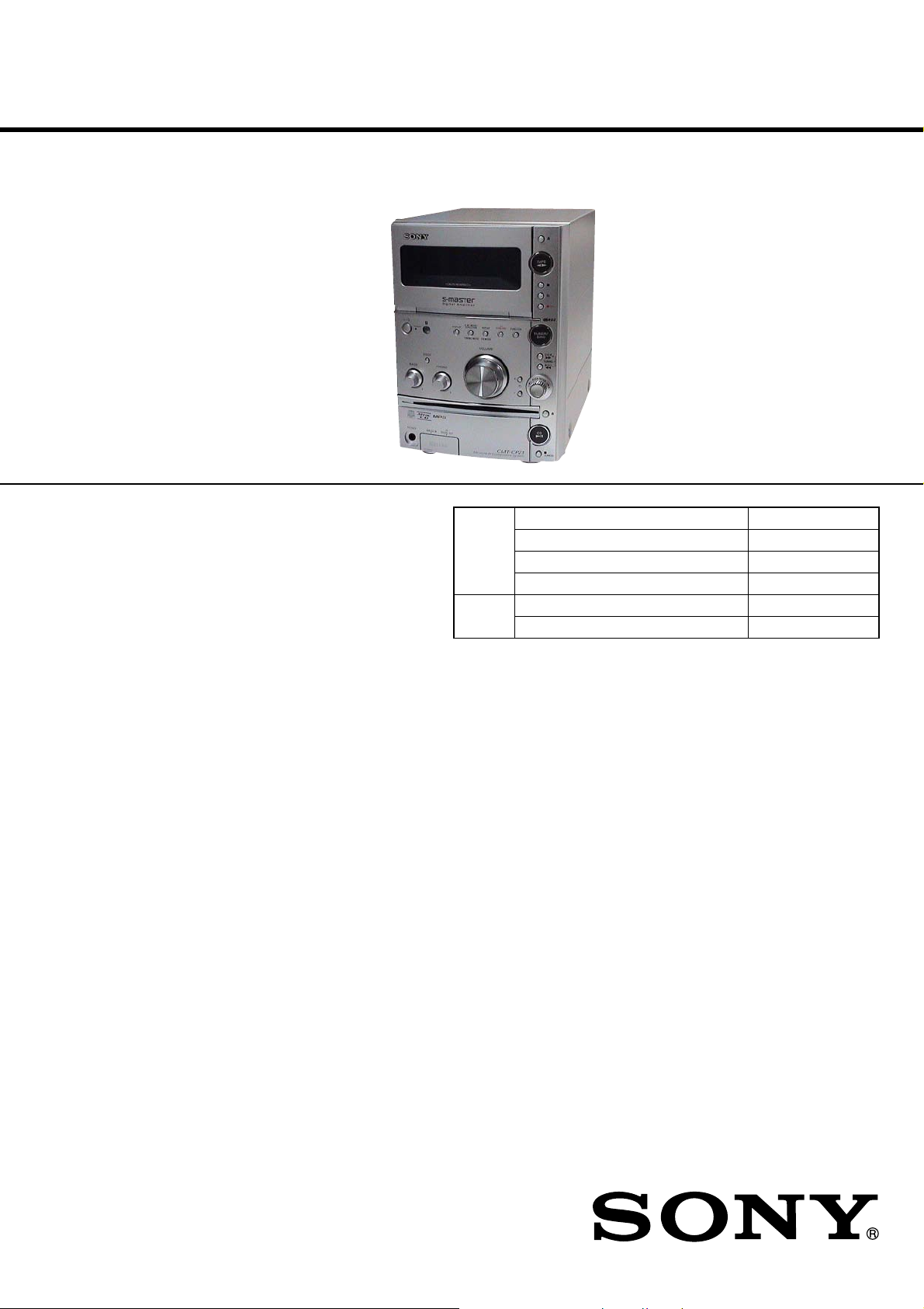
HCD-CPZ1
SERVICE MANUAL
Ver. 1.1 2005.05
HCD-CPZ1 is the amplifier, CD player, tape
deck and tuner section in CMT-CPZ1.
US and foreign patents licensed from Dolby
Laboratories.
CD CD Mechanism Type CDM80BH-F1BD83
Section Base Unit Name BU-F1BD83
TAPE Model Name Using Similar Mechanism NEW
Section Tape Transport Mechanism T ype CMAL1Z-255A
AEP Model
UK Model
Australian Model
Model Name Using Similar Mechanism NEW
Optical Pick-up Block Name
KSM-215DCP/C2NP
E Model
Amplifier section
European model:
DIN power output (rated): 60 + 60 watts (4 ohms at
1kHz, DIN)
Continuous RMS power output (refer en ce) :
75 + 75 watts ( 4 ohms at
1kHz, 10% THD)
Other models:
The following measured at AC 220 − 240 V, 50/60 Hz
DIN power output (rated) 60 + 60 watts
(4 ohms at 1 kHz, DIN)
Continuous RMS power output (refer en ce)
75 + 75 watts
(4 ohms at 1 kHz, 10%
THD)
Inputs
ANALOG IN (stereo mini jack):
Sensitivity 250 mV,
impedance 47 kilohms
Outputs
CD DIGITAL OUT: Optical Wavelength:
660 nm
PHONES (stereo mini jack):
accepts headphones with
an impedance of 8 ohms or
more
SPEAKER: accepts impedance of
4ohms
CD player section
System Compact disc and digital
audio system
SPECIFICATIONS
Laser Diode Properties Emissio n dur ation:
continuous
Laser Output: Less than
44.6 µW
(This output is the value
measurement at a distance
of 200 mm from the
objective lens surface on
the Optical Pick-up Block
with 7 mm aperture)
Frequency response 2 Hz − 20 kHz (±0.5 dB)
Wavelength 770 − 810nm
Tape deck section
Recording system 4-track 2-channel stereo
Frequency response 50 − 13,000 Hz (±3 dB),
using Sony TYPE I
cassettes
Tuner section
FM stereo, FM/AM superheterodyne tuner
FM tuner section
Tuning range 87.5 − 108.0 MHz
(50 kHz step)
Antenna FM lead antenna
Antenna terminals 75 ohms unbalanced
Intermediate frequency 10.7 MHz
AM tuner section
Tuning range
European, model: 531 − 1,602 kHz
(with the tuning interval
set at 9 kHz)
Other models: 531 − 1,602 kHz
(with the tuning interval
set at 9 kHz)
530 − 1,710 kHz
(with the tuning interval
set at 10 kHz)
Antenna AM loop antenna
Antenna terminals External antenna termi n al
Intermediate frequency 450 kHz
General
Power requirements
European model: 230 V AC, 50/60 Hz
Other models: 220 − 240 V AC, 50/60 Hz
Power consumption
European model: 60 watts
0.3 watts (in Power Saving
mode)
Other models: 60 watts
Dimensions (w/h/d) (excl. speakers):
Approx. 175 × 240 ×
295 mm
Mass (excl. speakers)
Amplifier/Tuner/Tape/CD section:
Approx. 3.8 kg
Design and specifications are subject to change
without notice.
9-879-454-02
2005E05-1
© 2005.05
COMPACT DISC DECK RECEIVER
Sony Corporation
Personal Audio Group
Published by Sony Engineering Corporation
HCD-CPZ1
Notes on chip component replacement
• Never reuse a disconnected chip component.
• Notice that the minus side of a tantalum capacitor may be
damaged by heat.
Flexible Circuit Board Repairing
• Keep the temperature of the soldering iron around 270 ˚C
during repairing.
• Do not touch the soldering iron on the same conductor of the
circuit board (within 3 times).
• Be careful not to apply force on the conductor when soldering
or unsoldering.
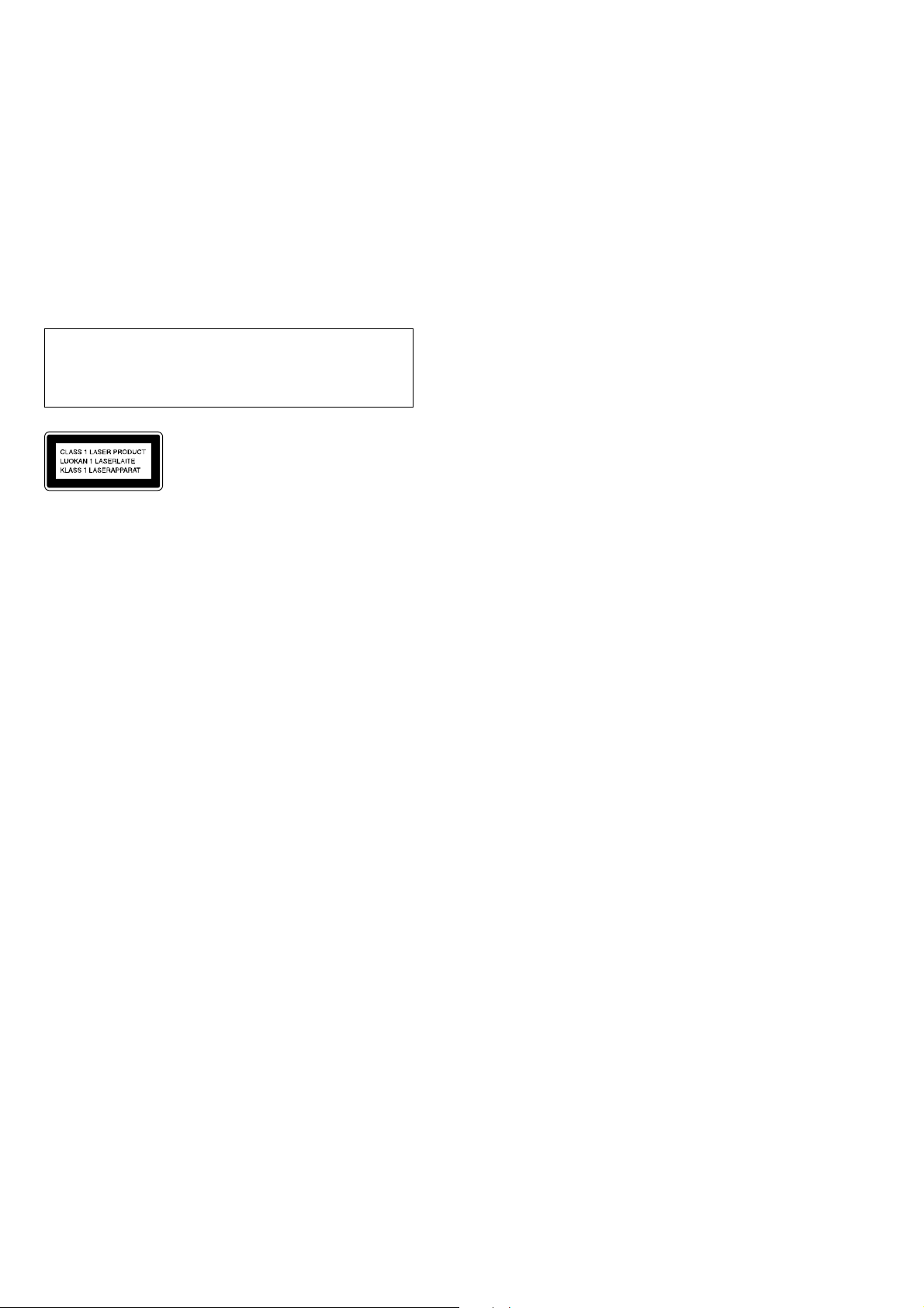
CAUTION
Use of controls or adjustments or performance of procedures
other than those specified herein may result in hazardous radiation
exposure.
This appliance is classified as
a CLASS 1 LASER product.
The CLASS 1 LASER
PRODUCT MARKING is
located on the rear exterior.
SAFETY-RELATED COMPONENT WARNING!!
COMPONENTS IDENTIFIED BY MARK 0 OR DOTTED LINE
WITH MARK 0 ON THE SCHEMATIC DIAGRAMS AND IN
THE PARTS LIST ARE CRITICAL TO SAFE OPERATION.
REPLACE THESE COMPONENTS WITH SONY PARTS WHOSE
PART NUMBERS APPEAR AS SHOWN IN THIS MANUAL OR
IN SUPPLEMENTS PUBLISHED BY SONY.
2

TABLE OF CONTENTS
HCD-CPZ1
1. SERVICING NOTES ............................................... 4
2. GENERAL ................................................................... 5
3. DISASSEMBLY
3-1. Disassembly Flow ........................................................... 6
3-2. Case ................................................................................. 7
3-3. Front Panel Section ......................................................... 7
3-4. TC Board, Mechanical Deck (CMAL1Z-255A) ............. 8
3-5. PANEL Board.................................................................. 8
3-6. MAIN Board.................................................................... 9
3-7. CD Mechanism Deck (CDM80BH-F1BD83) ................. 9
3-8. Chassis (Top) ................................................................... 10
3-9. Lever (Loading-L/R) ....................................................... 11
3-10. Lever (Disc Sensor), Lever (Disc Stop) .......................... 12
3-11. DRIVER Board,
Motor (Pulley) Assy (Loading) (M701) .......................... 12
3-12. BD Board......................................................................... 13
3-13. BU Section ...................................................................... 13
3-14. Optical Pick-up Block (KSM-215DCP).......................... 14
3-15. Lever (BU Lock) ............................................................. 14
3-16. Close Lever...................................................................... 15
3-17. Lever (DIR), Gear (IDL-B) ............................................. 15
3-18. Gear (IDL-C) ................................................................... 16
4. TEST MODE.............................................................. 17
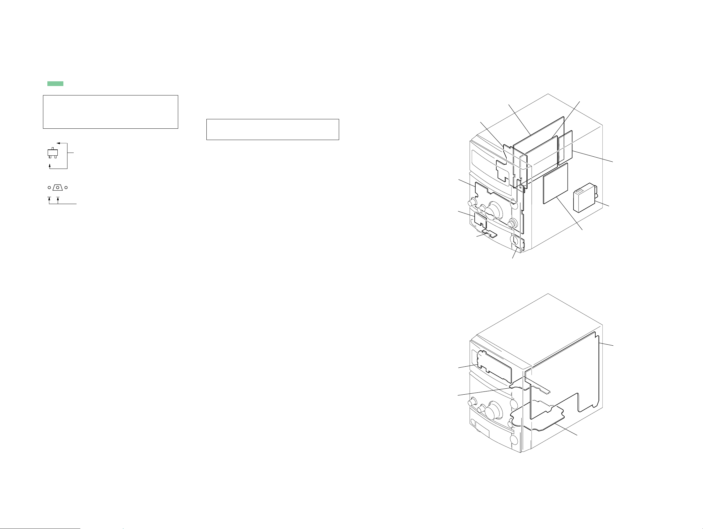
8. EXPLODED VIEWS
8-1. Case Section .................................................................... 58
8-2. Mechanical Deck (Tape) Section..................................... 59
8-3. Front Panel Section ......................................................... 60
8-4. Lid (TC) Section.............................................................. 61
8-5. Chassis Section................................................................ 62
8-6. Amp/Power Section......................................................... 63
8-7. CD Mechanism Deck Section-1
(CDM80BH-F1BD83)..................................................... 64
8-8. CD Mechanism Deck Section-2
(CDM80BH-F1BD83)..................................................... 65
8-9. CD Mechanism Deck Section-3
(CDM80BH-F1BD83)..................................................... 66
8-10. Base Unit Section (BU-F1BD83) .................................... 67
9. ELECTRICAL PARTS LIST................................ 68
5. MECHANICAL ADJUSTMENTS ....................... 19
6. ELECTRICAL ADJUSTMENTS ......................... 19
7. DIAGRAMS
7-1. Block Diagram
– CD SERVO/TAPE DECK/TUNER Section –.............. 20
7-2. Block Diagram – MAIN Section –.................................. 21
7-3. Block Diagram
– PANEL/KEY/POWER SUPPLY Section –.................. 22
7-4. Printed Wiring Board – BD Board – ............................... 24
7-5. Schematic Diagram – BD Board – .................................. 25
7-6. Printed Wiring Board – TC Board – ................................ 26
7-7. Schematic Diagram – TC Board – .................................. 27
7-8. Printed Wiring Board – DRIVER Board –...................... 28
7-9. Schematic Diagram – DRIVER Board –......................... 28
7-10. Printed Wiring Board – MAIN Board – .......................... 29
7-11. Schematic Diagram – MAIN Board (1/2) – .................... 30
7-12. Schematic Diagram – MAIN Board (2/2) – .................... 31
7-13. Schematic Diagram – AMP Board (1/2) – ...................... 32
7-14. Schematic Diagram – AMP Board (2/2) – ...................... 33
7-15. Printed Wiring Board – AMP Board – ............................ 34
7-16. Printed Wiring Board – SP Board – ................................ 35
7-17. Schematic Diagram – SP Board – ................................... 35
7-18. Printed Wiring Board – LCD Board –............................. 36
7-19. Schematic Diagram – LCD Board –................................ 37
7-20. Printed Wiring Boards – PANEL Section –..................... 38
7-21. Schematic Diagram – PANEL Section –......................... 39
7-22. Printed Wiring Boards – JACK Section – ....................... 40
7-23. Schematic Diagram – JACK Section –............................ 41
7-24. Printed Wiring Board – SW POWER Board – ................ 42
7-25. Schematic Diagram – SW POWER Board –................... 43
7-26. Printed Wiring Board – SUB POWER Board – .............. 44
7-27. Schematic Diagram – SUB POWER Board – ................. 45
3
HCD-CPZ1
Ver. 1.1
SECTION 1
SERVICING NOTES
NOTES ON HANDLING THE OPTICAL PICK-UP
BLOCK OR BASE UNIT
The laser diode in the optical pick-up block may suffer electrostatic
break-down because of the potential difference generated by the
charged electrostatic load, etc. on clothing and the human body.
During repair, pay attention to electrostatic break-down and also
use the procedure in the printed matter which is included in the
repair parts.
The flexible board is easily damaged and should be handled with
care.
NOTES ON LASER DIODE EMISSION CHECK
The laser beam on this model is concentrated so as to be focused on
the disc reflective surface by the objective lens in the optical pickup block. Therefore, when checking the laser diode emission,
observe from more than 30 cm away from the objective lens.
UNLEADED SOLDER
Boards requiring use of unleaded solder are printed with the leadfree mark (LF) indicating the solder contains no lead.
(Caution: Some printed circuit boards may not come printed with
the lead free mark due to their particular size)
: LEAD FREE MARK
Unleaded solder has the following characteristics.
• Unleaded solder melts at a temperature about 40 °C higher
than ordinary solder.
Ordinary soldering irons can be used but the iron tip has to be
applied to the solder joint for a slightly longer time.
Soldering irons using a temperature regulator should be set to
about 350 °C.
Caution: The printed pattern (copper foil) may peel away if
the heated tip is applied for too long, so be careful!
• Strong viscosity
Unleaded solder is more viscou-s (sticky, less prone to flow)
than ordinary solder so use caution not to let solder bridges
occur such as on IC pins, etc.
• Usable with ordinary solder
It is best to use only unleaded solder but unleaded solder may
also be added to ordinary solder.
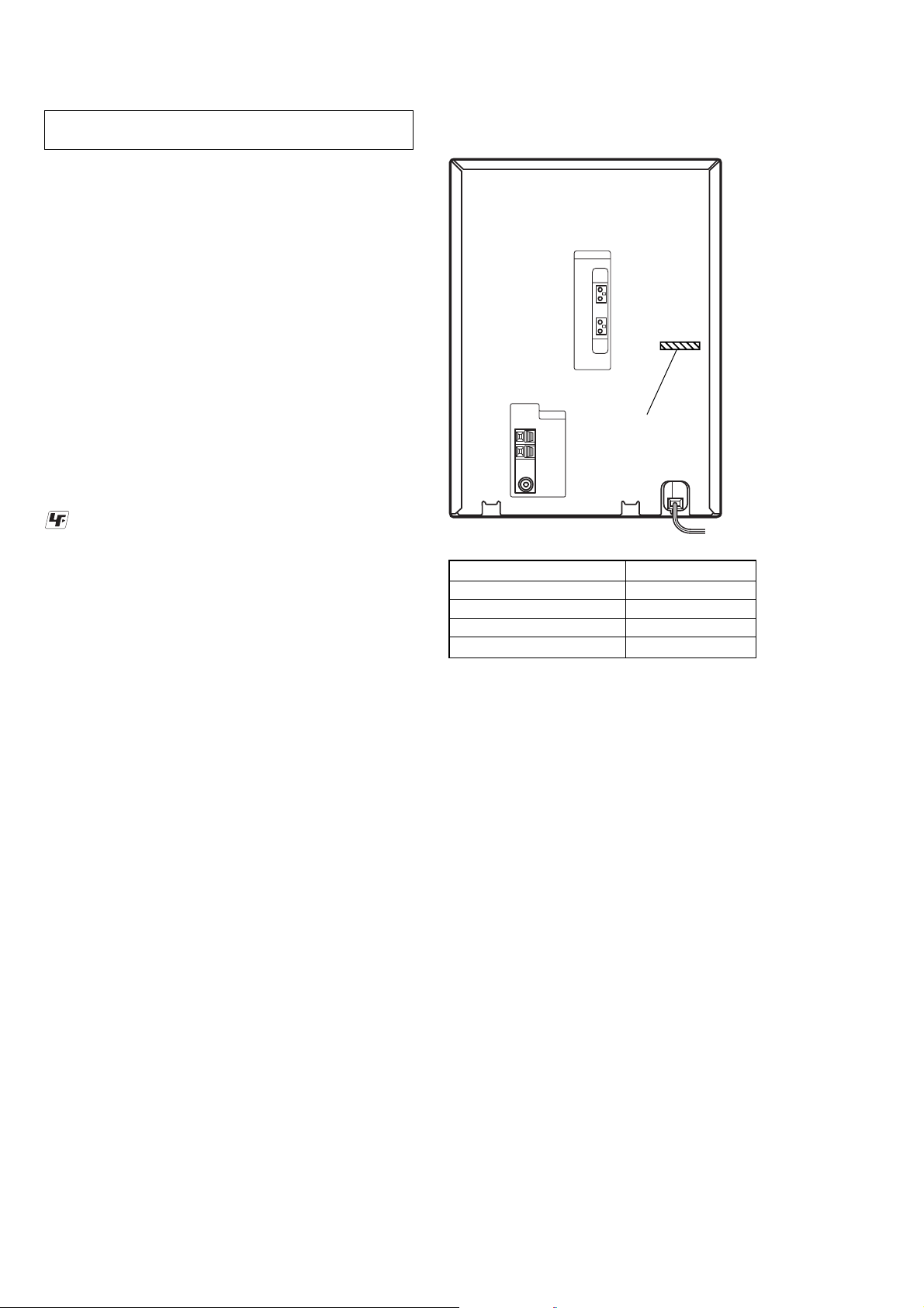
• MDDEL IDENTIFICATION
– Back Panel –
PART No.
Model PART No.
AEP, UK, East European models 2-514-690-0[]
Australian model 2-514-690-1[]
Korean model 2-514-690-2[]
Singapore model 2-514-690-3[]
4
Main unit
ALPHABETICAL ORDER
ANALOG IN jack ws
BASS control wh
CANCEL w;
CD DIGITAL OUT jack wd
CD SYNCHRO 0
DIRECTION wk
Disc slot wf
DISPLAY wl
Display window 3
DSGX wj
FM MODE 9
FUNCTION qs
Jog dial qf
PHONES jack wa
PLAY MODE wk
PUSH ENTER qg
Remote sensor 2
REPEAT 9
TREBLE control wg
TUNER/BAND qa
TUNING MODE wk
TUNING + / – qd
VOLUME control ql
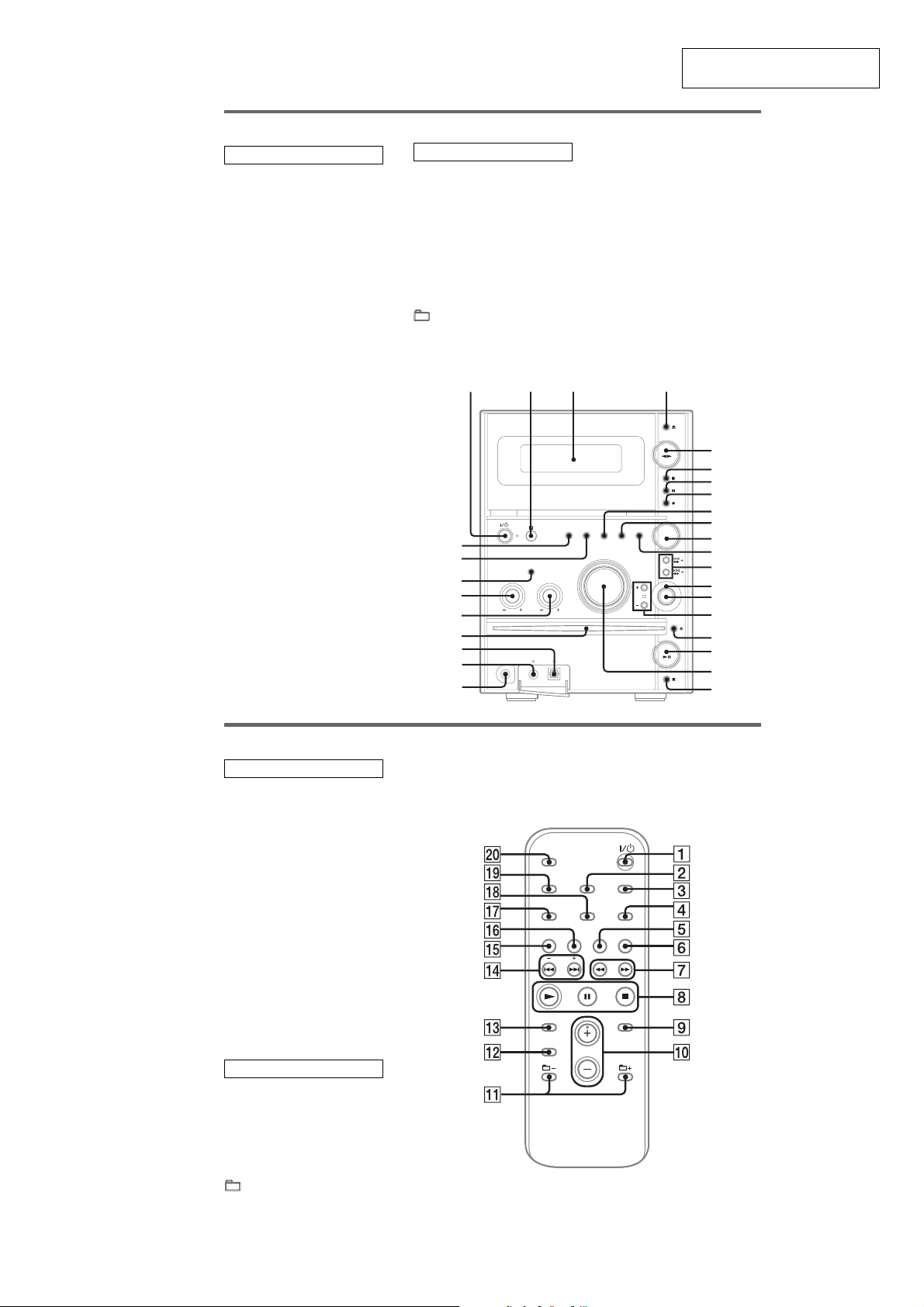
SECTION 2
GENERAL
BUTTON DESCRIPTIONS
?/1 (power) 1
TAPE Z (eject) 4
TAPE nN (play) 5
TAPE x (stop) 6
TAPE X (pause) 7
TAPE z REC (record) 8
lm/ML (rewind/fast
forward, go back/go forward)
qd
+/– (select group) qh
CD Z (eject) qj
CD NX (play) qk
CD x (stop) w;
1
wl
wk
wj
wh
wg
wf
wd
ws
wa
2
3
HCD-CPZ1
This section is extracted from
instruction manual.
4
5
6
7
8
9
0
qa
qs
qd
qf
qg
qh
qj
qk
ql
w;
Remote control
ALPHABETICAL ORDER
CD qh
CLEAR qd
CLOCK/TIMER SELECT 2
CLOCK/TIMER SET 3
DISPLAY ql
ENTER 9
EQ qs
FM MODE 4
FUNCTION 6
PLAY MODE qk
REPEAT 4
SLEEP w;
TAPE qg
TUNER BAND 5
TUNER MEMORY qj
TUNING MODE qk
VOLUME +/– q;
BUTTON DESCRIPTIONS
?/1 (power) 1
m/M (rewind/fast forward)
7
N (play) 8
X (pause) 8
x (stop) 8
+/– (select group) qa
./> (go back/go forward)
qf
+/– (tuning) qf
5
HCD-CPZ1
• This set can be disassembled in the order shown below.
3-1. DISASSEMBLY FLOW
SET
3-2. CASE
(Page 7)
3-3. FRONT PANEL SECTION
(Page 7)
SECTION 3
DISASSEMBLY
3-4. TC BOARD,
MECHANICAL DECK
(CMAL1Z-255A)
(Page 8)
3-5. PANEL BOARD
(Page 8)
3-8. CHASSIS (TOP)
(Page 10)
3-9. LEVER (LOADING-L/R)
(Page 11)
3-6. MAIN BOARD
(Page 9)
3-7. CD MECHANISM DECK
(CDM80BH-F1BD83)
(Page 9)
3-11. DRIVER BOARD,
MOTOR (PULLEY) ASSY
(LOADING) (M701)
(Page 12)
3-12. BD BOARD
3-10. LEVER (DISC SENSOR),
LEVER (DISC STOP)
(Page 12)
(Page 13)
3-13. BU SECTION
(Page 13)
3-14. OPTICAL PICK-UP BLOCK
(KSM-215DCP)
(Page 14)
3-15. LEVER (BU LOCK)
(Page 14)
3-16. CLOSE LEVER
(Page 15)
3-17. LEVER (DIR),
GEAR (IDL-B)
(Page 15)
3-18. GEAR (IDL-C)
(Page 16)
6
Note: Follow the disassembly procedure in the numerical order given.
)
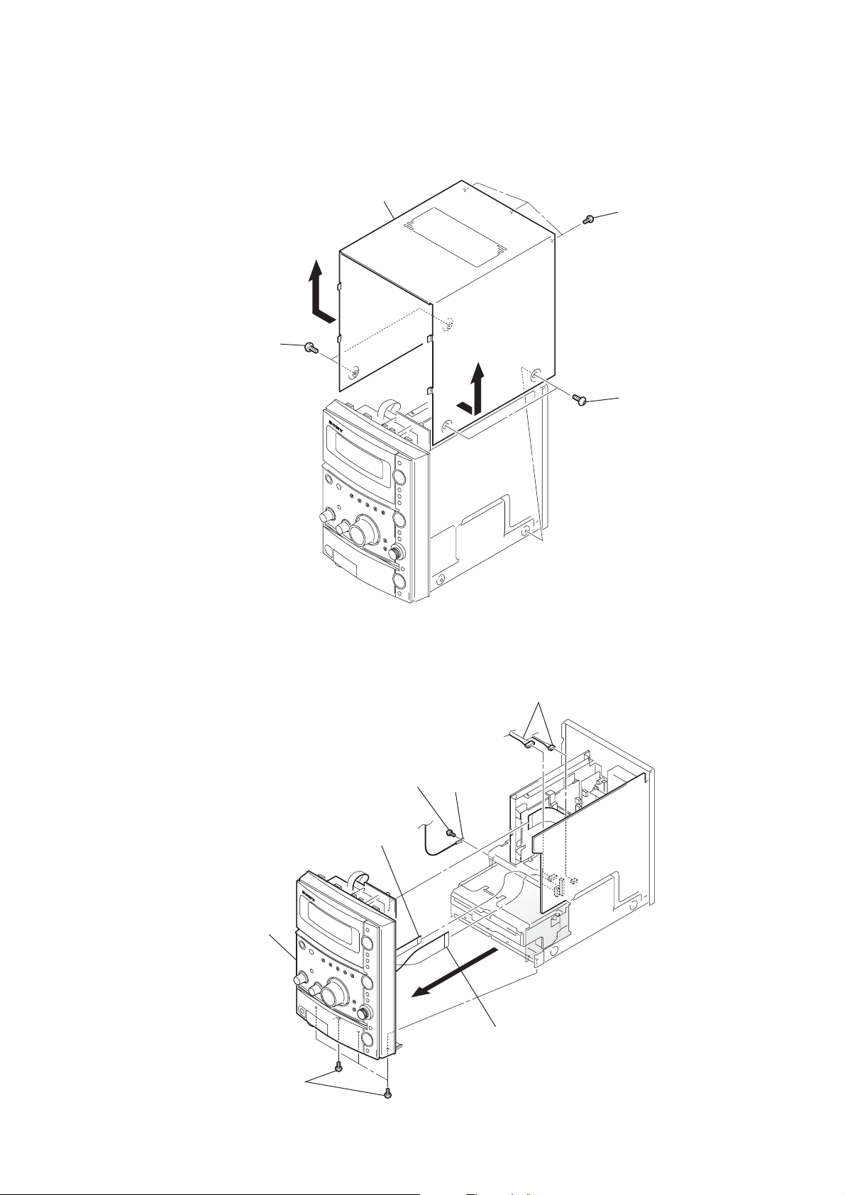
3-2. CASE
4
case
3
1
two screws
(case 3 TP2)
2
three screws
(B3)
HCD-CPZ1
3-3. FRONT PANEL SECTION
1
screw (B3)
2
3
terminal
5
two connectors
(CN303, CN307)
1
two screws
(case 3 TP2
7
front panel section
6
four screws
(B3)
4
wire (flat type) (9 core)
(CN304)
3
wire (flat type) (19 core)
(CN305)
7
HCD-CPZ1
3-4. TC BOARD, MECHANICAL DECK (CMAL1Z-255A)
6
terminal
5
four screws
(B3)
1
wire (flat type) (8 core)
4
TC board
3-5. PANEL BOARD
q;
lid (TC) section
5
torsion spring
(lid TC2)
2
knob (VOL)
8
two bosses
3
knob (TRE)
4
7
mechanical deck
(CMAL1Z-255A)
knob (BASS)
3
connector
2
three screws
(PTPWH 2)
1
knob (UD)
torsion spring
(lid TC2)
qs
PANEL board
qa
six screws
(B2.6)
7
9
bracket (TC)
6
three screws
(B2.6)
8
3-6. MAIN BOARD
n
5
3
wire (flat type) (21 core)
(CN302)
two connectors
(CN300, CN306)
5
two connectors
(CN201, CN202)
2
back panel
1
four screws
(B3)
1
three screws
(B3)
8
HCD-CPZ1
Ver. 1.1
MAIN board
4
wire (flat type) (23 core)
(CN308)
7
wire (flat type) (15 core) (AEP, UK and East European models),
wire (flat type) (11 core) (Singapore, Korean and Australian models)
(CN309)
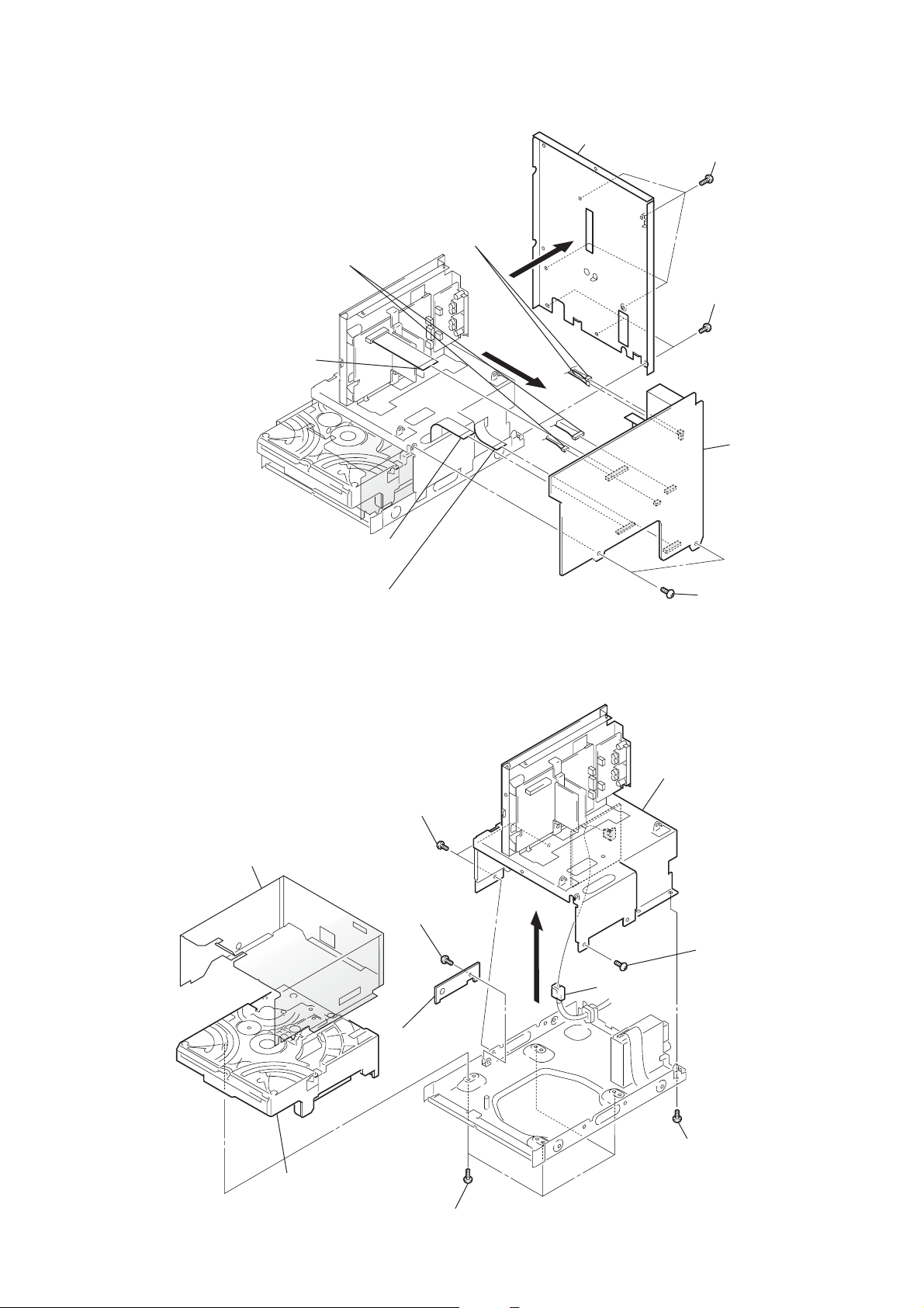
3-7. CD MECHANISM DECK (CDM80BH-F1BD83)
3
two screws
(B3)
7
cover (CDM)
5
screw (B3)
1
connector
(CN990)
6
two screws (B3)
4
AMP/POWER sectio
3
screw
(B3)
9
CD mechanism deck
(CDM80BH-F1BD83)
6
cover board
8
four screws
(B3)
2
screw (B3)
9
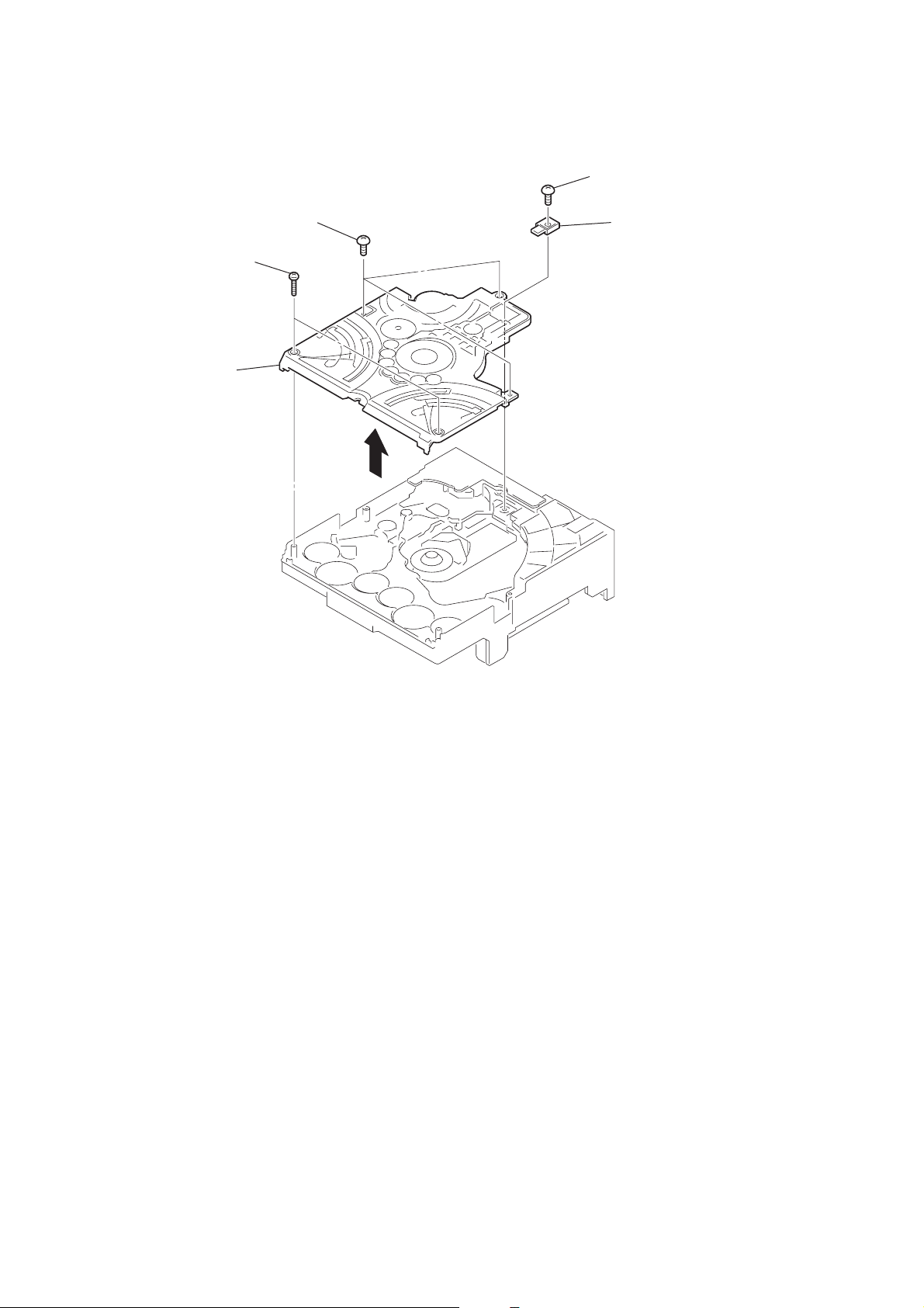
HCD-CPZ1
)
3-8. CHASSIS (TOP)
4
two screws
(P 2
5
chassis (top)
×
10)
3
three screws
(BVTP 2.6)
1
screw
(BVTP 2.6 )
2
lever (CL UP2
10
3-9. LEVER (LOADING-L/R)
)
HCD-CPZ1
6
lever (loading-R)
2
spr-T (loading-R) spr-T (loading-L)
5
two hooks
1
3
two hooks
4
lever (loading-L
PRECAUTION DURING LEVER (LOADING-R / L) INSTALLATION
Align the horizontal position.
lever (loading-L)
Install the
both levers so that they move symmetrically.
lever (loading-R)
11
HCD-CPZ1
d
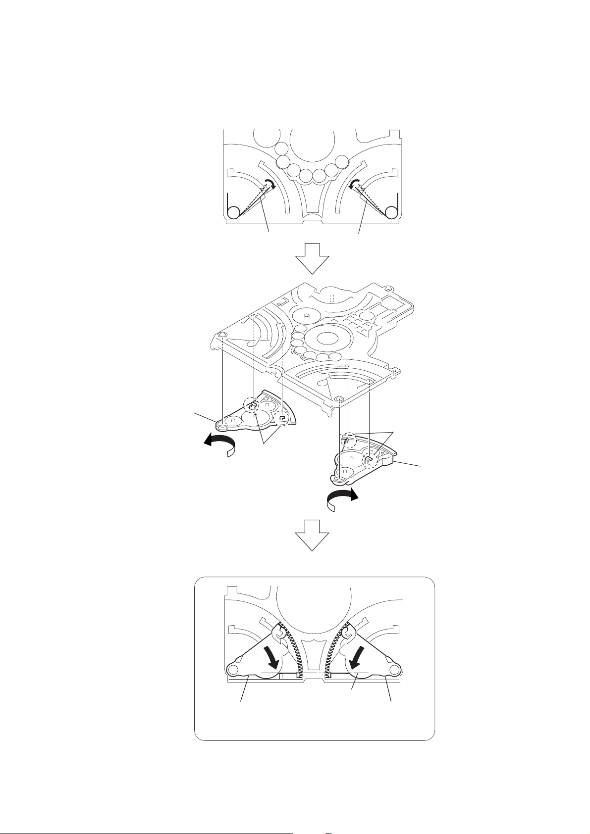
3-10. LEVER (DISC SENSOR), LEVER (DISC ST OP)
1
gear (cap)
2
gear (IDL-L)
PRECAUTION DURING LEVER (DISC STOP) INSTALLATION
5
two hooks
3
two claws
6
lever (disc stop)
4
lever (disc sensor)
hole
Install the lever (disc stop) so that the both holes
are aligned.
3-11. DRIVER BOARD, MOTOR (PULLEY) ASSY (LOADING) (M701)
2
two screws
(BVTP 2.6)
3
Remove soldering
from the two points.
hole
4
DRIVER boar
chassis (top)
lever (disc stop)
12
5
motor (pully) assy (loading)
(M701)
1
belt (MOT)
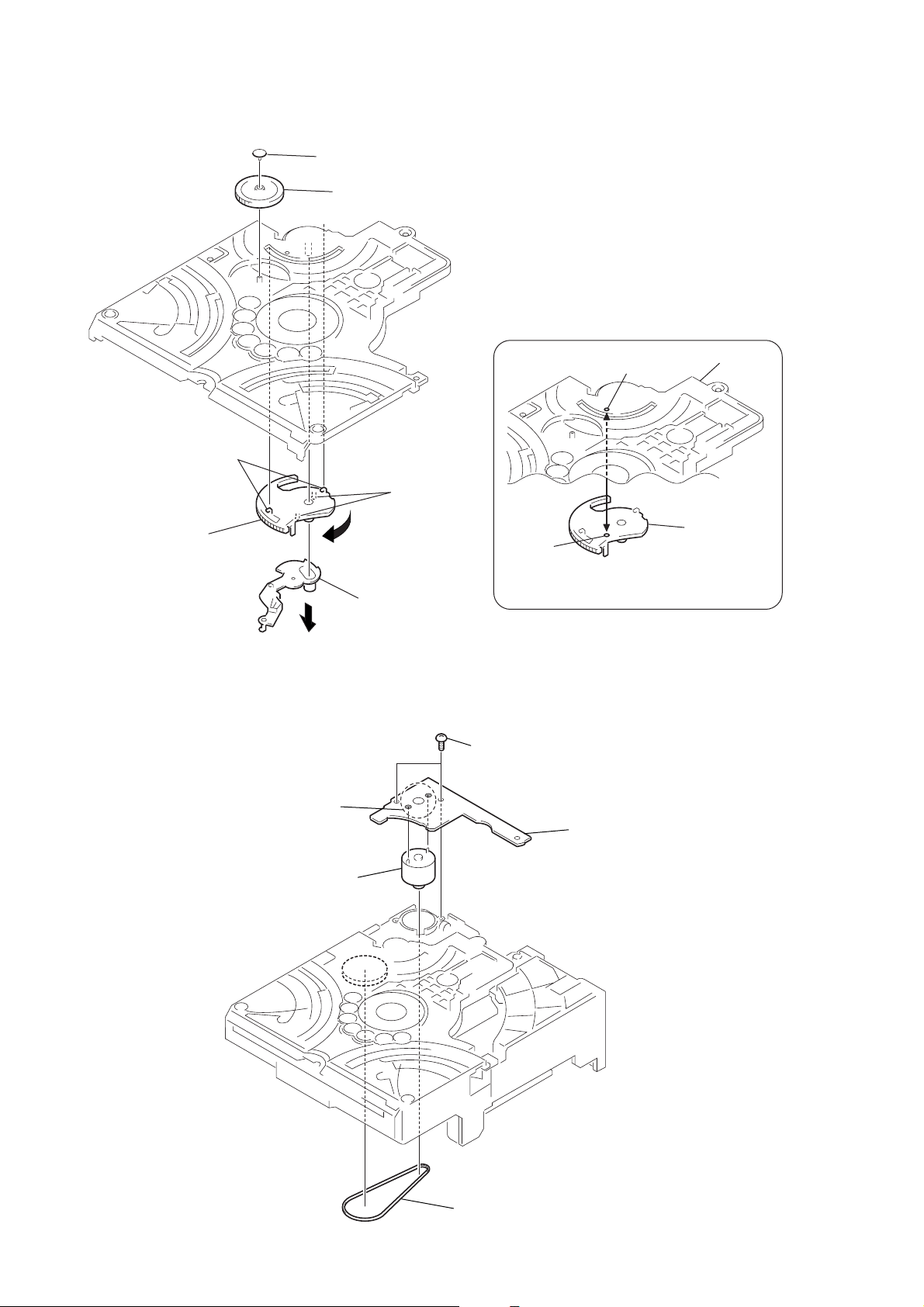
3-12. BD BOARD
)
2
5
BD board
wire (flat type) (16 core)
(CN301)
1
Remove soldering
from the four points.
3
4
HCD-CPZ1
sheet
wire (flat type) (23 core
(CN102)
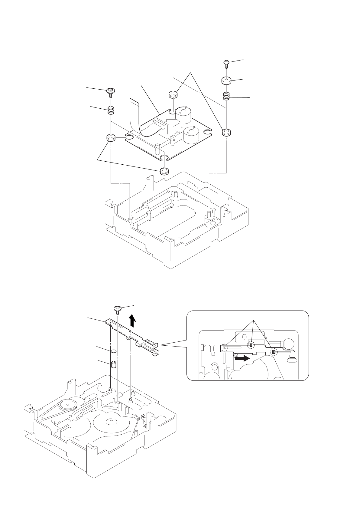
3-13. BU SECTION
6
BU section
4
screw
(PTPWH M2.6)
3
spring (holder down B)
5
screw
(PTPWH M2.6)
2
lever (CL UP2)
1
screw
(BVTP 2.6 )
13
HCD-CPZ1
)
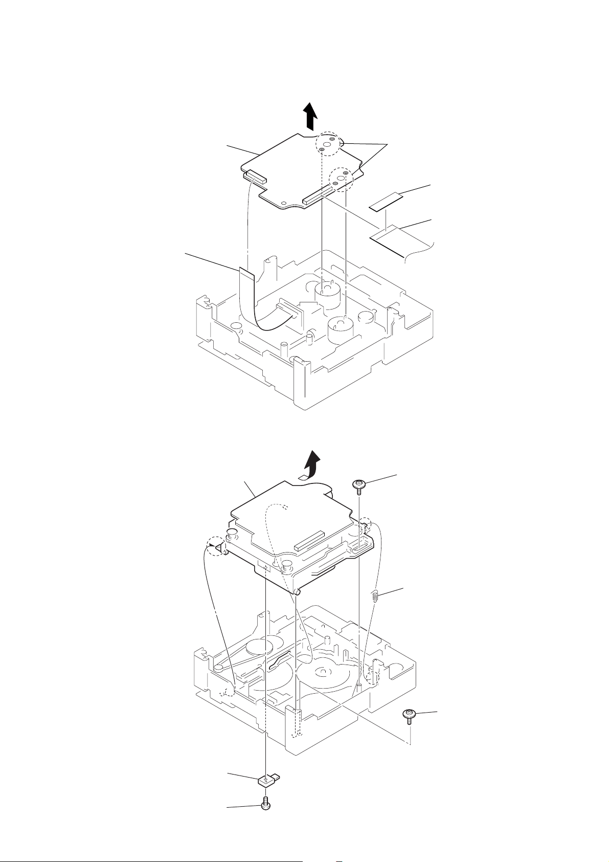
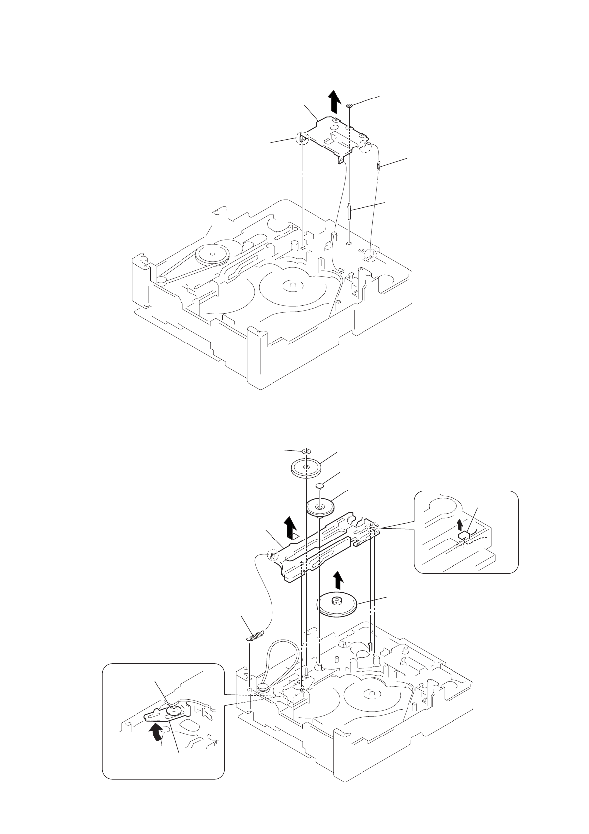
3-14. OPTICAL PICK-UP BLOCK (KSM-215DCP)
7
4
two screws
(PTPWH M2.6)
5
two coil springs (insulator)
6
two insulators
optical pick-up block
(KSM-215DCP)
6
two insulators
1
two screws
(BTTP M2.6)
2
two stoppers (BU)
3
two coil springs (insulator
3-15. LEVER (BU LOCK)
5
lever (BU lock)
2
gear (cap)
3
gear (BU lock)
1
screw (PTPWH M2.6)
4
three hooks
2
14
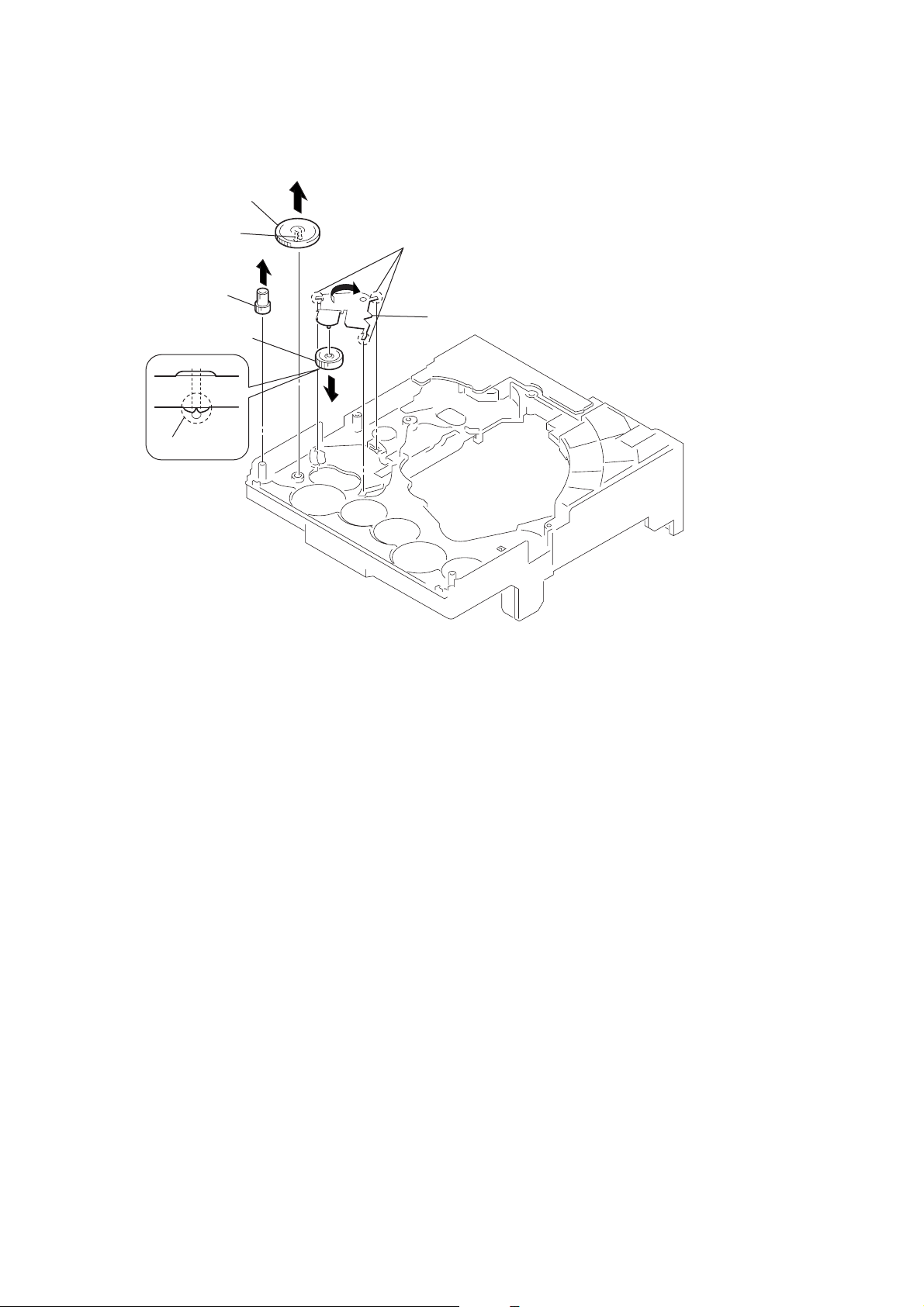
3-16. CLOSE LEVER
e
3
5
claw
close lever
1
washer (3-1-0.4)
2
4
shaft disc stop
HCD-CPZ1
SPR-E lever clos
3-17. LEVER (DIR), GEAR (IDL-B)
2
capstan retaining ring
9
1
tension coil spring (DIR)
6
Loosen the screw.
lever (DIR)
3
pulley (gear)
4
gear (cap)
5
gear (IDL-A)
q;
gear (IDL-B)
8
stopper
7
Hold the Release lever
and change the direction.
15
HCD-CPZ1
3-18. GEAR (IDL-C)
3
2
1
gear (IDL-F)
7
6
gear (IDL-D)
two claws
gear (IDL-C)
claw
4
three hooks
5
lever (gear loading)
16
SECTION 4
TEST MODE
HCD-CPZ1
[COMMON TEST MODE]
• This mode is used to check operations of Amplifier.
Procedure:
1. Press the I/1 key to turn the power ON.
2. Press three keys of [DSGX] and x (CD) and [PUSH ENTER]
JOG simultaneously.
3. When the COMMON test mode is activated, “s” blinks on
the liquid crystal display.
4. Turn the [BASS] knob counterclockwise, “TONE MIN” is
displayed on the liquid crystal display. Turn the [BASS] knob
clockwise, “TONE MAX” is displayed on the liquid crystal
display.
Turn the [TREBLE] knob clockwise or counterclockwise,
“TONEFLAT” is displayed on the liquid crystal display.
Turn the [VOLUME] knob counterclockwise, “VOL MIN” is
displayed on the liquid crystal display. Turn the [VOLUME]
knob clockwise, “VOL MAX” is displayed on the liquid crystal
display.
5. To release this mode, press the I/1 key.
[PANEL TEST MODE]
• This mode is used to check the liquid crystal display, LED,
model, destination, software version and key.
Procedure:
1. Press the I/1 key to turn the power ON.
2. Press three keys of [DSGX], [DISPLAY] and x (CD)
simultaneously.
3. Liquid crystal display and LEDs are all turned on.
4. When you want to enter the model, destination and version display
mode, press the [PLAY MODE/DIRECTION/TUNING MODE] key.
The model and destination are displayed alternately on the
liquid crystal display.
5. Each time [PLAY MODE/DIRECTION/TUNING MODE] key is
pressed, the display changes starting from MC version, GC
version, CD version, CDD version, CDMA version, CDMB
version, BDA version, BDB version, ST version, TA version,
TM version, and TC version this order , and returns to the MC
version display on the liquid crystal display.
6. Press the [REPEAT/FM MODE] key, the key check mode is
activated.
7. In the key check mode, the liquid crystal display displays “K0”.
Each time a key is pressed, “K” value increases. However,
once a key is pressed, it is no longer taken into account.
8. When [FUNCTION] key is pressed while the version numbers
are being displayed except model and destination, year, month
and day of the software creation display. When [FUNCTION]
key is pressed again, the display returns to the software version
display. When [PLAY MODE/DIRECTION/TUNING MODE] key
is pressed while year, month and day of the software creation
are being displayed, the year, month and day of creation of
the software versions are displayed on the liquid crystal display
in the same order of version display.
9. To release this mode, press three keys in the same manner as
step 2, or disconnect the power cord.
[COLD RESET]
• The cold reset clears all data including preset data stored in
the RAM to initial conditions. Execute this mode when
returning the set to the customer.
Procedure:
1. Press the I/1 key to turn the power ON.
2. Press three keys of I/1 , [DISPLAY] and x (TAPE)
simultaneously.
3. The liquid crystal display becomes blank instantaneously, and
the set is reset.
[SHIP MODE (NO MEMORY CLEAR)]
• This mode moves the optical pick-up to the position durable
to vibration. Use this mode when returning the set to the
customer after repair.
Procedure:
1. Press the I/1 key to turn the power ON.
2. Press the [FUNCTION] key to select “CD”.
3. Press three keys of [DSGX], x (CD) and +simultaneously and the ship mode is set.
[SHIP MODE (MEMORY CLEAR)]
• This mode moves the optical pick-up to the position durable
to vibration. Use this mode when returning the set to the
customer after repair.
Procedure:
1. Press the I/1 key to turn the power ON.
2. Press the [FUNCTION] key to select “CD”.
3. Press three keys of [DSGX], x (CD) and – simultaneously.
4. After the “ST ANDBY” display blinks, “LOCK” is displayed
on the liquid crystal display, and the ship mode is set.
[CD SLOT LOCK MODE]
• This mode is used to unable to take sample disc out of disc
slot in the shop.
Procedure:
1. Press the I/1 key to turn the power ON.
2. Press the [FUNCTION] key to select “CD”.
3. While pressing the Z (CD) key, press the x (CD) key for
5 seconds.
4. The message “LOCKED” is displayed on the liquid crystal
display and the disc slot is locked. (Even if pressing
the Z (CD) key, the message “LOCKED” is displayed on
the liquid crystal display and the disc slot is locked)
5. To release from this mode, pressing the Z (CD) key, press
the x (CD) key for 5 seconds.
6. The message “UNLOCKED” is displayed on the liquid crystal
display and the disc slot is unlocked.
[CD SERVICE MODE]
• This mode can run the CD sled motor freely. Use this mode,
for instance, when cleaning the optical pick-up.
Procedure:
1. Press the I/1 key to turn the power ON.
2. Press the [FUNCTION] key to select “CD”.
3. Press three keys of [PLAY MODE/DIRECTION/TUNING MODE],
M L and x (CD) simultaneously.
4. Press the M L key to move the optical pick-up to outside
track, or press the l m key to inside track.
5. Press the CD u key, “LD OFF” is displayed and laser diode
is turned off. Each time CD u key is pressed, laser diode
ON/OFF seitch is performed.
6. To release this mode, press the I/1 key.
[CD ERROR CODE MODE]
• This mode can be used for error display of CD section.
Procedure:
1. Press the I/1 key to turn the power ON.
2. Press the [FUNCTION] key to select “CD”.
3. Press three keys of [PLAY MODE/DIRECTION/TUNING MODE],
+ and x (CD) simultaneously.
Note: Error code is not displayed on the liquid crystal display.
17

HCD-CPZ1
Ver. 1.1
[CD SERVO TEST MODE]
• This mode used to ckeck operation of optical pick-up.
Procedure:
1. Press the I/1 key to turn the power ON.
2. Press the [FUNCTION] key to select “CD”.
3. Press three keys of [PLAY MODE/DIRECTION/TUNING MODE],
l m and x (CD) simultaneously.
4. When the CD servo test mode is activated, optical pick-up
moves.
[CD POWER MANAGE]
This mode is for switch the CD power supply on/off. Even if this
state pulls out AC plug, it is held.
Procedure:
1. Press the I/1 button to turn the power on.
2. Press the [FUNCTION] button to select CD function.
3. Press the I/1 button again to turn the power off (standby).
4. While pressing the x (CD) button, press the I/1 button.
5. It turns power on and display “CD POWER”, then display
“ON” or “OFF”.
[CHANGE-OVER THE AM TUNING INTERVAL]
(Singapore and Korean models)
The AM tuning interval can be changed over 9 kHz or 10 kHz.
Procedure:
1. Press the I/1 button to turn the power on.
2. Press the [TUNER, BAND] button to select TUNER (AM)
function.
3. Press the I/1 button again to turn the power off (standby).
4. While pressing the [TUNING +] button, press the I/1 button.
5. It turns power on and display “STEP 9kHz” or “STEP 10kHz”,
and thus the tuning interval is changed over.
18
SECTION 5
r
e
V
forward
reverse
MECHANICAL ADJUSTMENTS
HCD-CPZ1
SECTION 6
ELECTRICAL ADJUSTMENTS
PRECAUTION
1. Clean the following parts with a denatured alcohol-moistened
swab:
record/playback heads pinch rollers
erase head rubber belts
capstan idlers
2. Demagnetize the record/playback head with a head de-
magnetizer.
3. Do not use a magnetized screwdriver for the adjustments.
4. After the adjustments, apply suitable locking compound to
the parts adjusted.
5. The adjustments should be performed with the rated power
supply voltage unless otherwise noted.
TORQUE MEASUREMENT
Mode
FWD
FWD
back tension
REV
REV
back tension
FF/REW
FWD tension
REV tension
Torque meter
CQ-102C
CQ-102C
CQ-102RC
CQ-102RC
CQ-201B
CQ-403A
CQ-403R
Meter reading
3.06 N • m to 6.96 N • m
31 to 71 g • cm
(0.43 – 0.98 oz • inch)
0.19 N • m to 0.58 N • m
2 to 6 g • cm
(0.02 – 0.08 oz • inch)
3.06 N • m to 6.96 N • m
31 to 71 g • cm
(0.43 – 0.98 oz • inch)
0.19 N • m to 0.58 N • m
2 to 6 g • cm
(0.02 – 0.08 oz • inch)
6.96 N • m to 14.02 N • m
71 to 143 g • cm
(0.98 – 1.99 oz • inch)
9.80 N • m
100 g or more
(3.53 oz or more)
9.80 N • m
100 g or more
(3.53 oz or more)
0 dB=0.775 VDECK SECTION
1. Demagnetize the record/playback head with a head
demagnetizer.
2. Do not use a magnetized screwdriver for the adjustments.
• Test Tape
Tape Signal Used for
P-4-A063 6.3 kHz, -10 dB Azimuth Adjustment
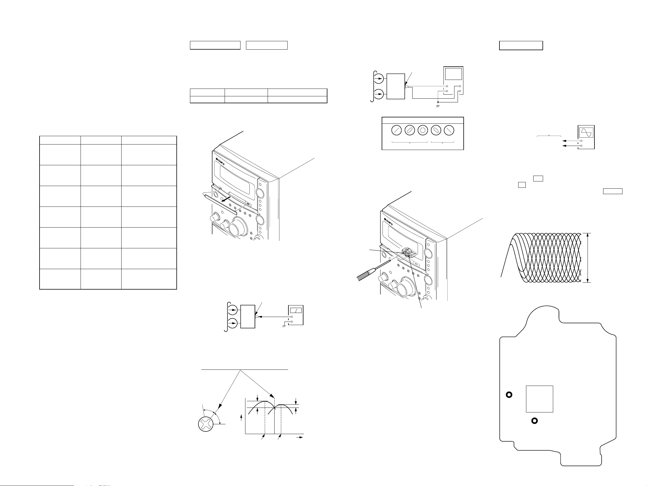
RECORD/PLA YBA CK HEAD AZIMUTH ADJUSTMENT
Note: Remove the cover (azimuth) before this adjustment.
Procedure:
1. Mode: Playback
test tape
P-4-A063
(6.3 kHz, –10 dB)
HP/MD board
PHONES jack
(J982)
level mete
3. Mode: Playback
test tape
P-4-A063
(6.3 kHz, –10 dB)
in phase 45°90°135°180
HP/MD board
PHONES jack
(J982)
set
waveform of oscilloscope
good
wrong
oscilloscope
H
V
°
4. After the adjustments, apply suitable locking compound to
the pats adjusted.
Adjustment Location: Record/Playback/Erase Head
CD SECTION
Note:
1. CD Block is basically constructed to operate without adjustment.
2. Use YEDS-18 disc (3-702-101-01) unless otherwise indicated.
3. Use an oscilloscope with more than 10 MW impedance.
4. Clean the object lens by an applicator with neutral deter gent when the
signal level is low than specified value with the following checks.
5. Check the focus bias check when optical pick-up block is replaced.
FOCUS BIAS CHECK
oscilloscop
(DC range)
BD board
TP (RFACI)
TP (VC)
Procedure :
1. Connect oscilloscope to TP (RFACI) and TP (VC) on the BD
board.
2. Press the I/1 button to turn the power ON, and press
the Z (CD) button to open the CD disc tray.
3. Set disc (YEDS-18) on the tray and press the CD u button
to playback.
4. Confirm that oscilloscope waveform is as sho wn in the figure
below. (eye pattern)
A good eye pattern means that the diamond shape (◊) in the
center of the waveform can be clearly distinguished.
Checking Location:
– BD Board (Conductor Side) –
+
–
VOLT/DIV: 200 m
TIME/DIV: 500 ns
level:
0.9
±
0.4 Vp-p
HCD-CPZ1
set
+
–
2. Turn the adjustment screw and check output peaks. If the peaks
do not match for L-CH and R-CH, turn the adjustment screw
so that outputs match within 1dB of peak.
Output
level
within
1dB
L-CH
peak
R-CH
peak
within
1dB
Screw
position
TP
(VC)
IC201
TP
(RFACI)
L-CH
peak
R-CH
Screw
position
peak
1919
HCD-CPZ1
Ver. 1.1
SECTION 7
DIAGRAMS
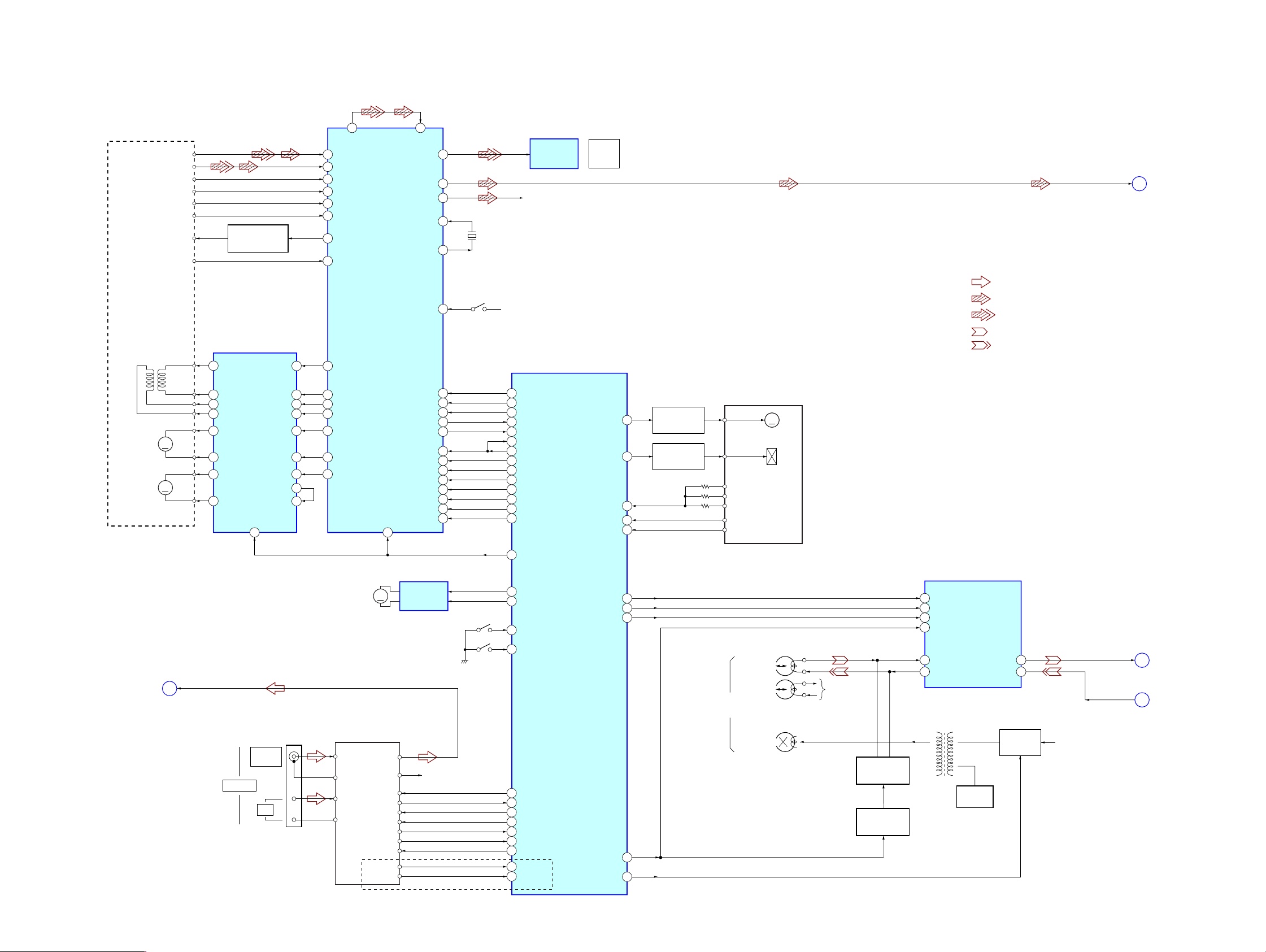
7-1. BLOCK DIAGRAM – CD SERVO/TAPE DECK/TUNER Section –
OPTICAL
PICK-UP BLOCK
(KSM-215DCP)
2-AXIS
DEVICE
FCS+
A
B
C
D
E
F
LD
PD
FOCUS/TRACKING COIL DRIVER,
SLED/SPINDLE MOTOR DRIVER
12
CH2OUTF
AUTOMATIC
POWER CONTROL
Q321
IC402
CH2FIN
6
70
RFACO
57
A
58
B
59
C
60
D
50
E
51
F
66
LD
67
PD
CD DSP
IC201
45
FFDR
71
RFACI
DOUT
AOUT1
AOUT2
XTAO
SSTP
XTAI
101
112
117
109
108
39
16.9344MHz
S201
(LIMIT)
X202
R-CH
D +3.3V
OPTICAL
TRANSCEIVER
IC981
SYSTEM CONTROLLER
IC301 (1/3)
CD
DIGITAL
OUT
• R-ch is omitted due to same as L-ch.
• SIGNAL PATH
: TUNER
: CD PLAY (ANALOG)
: CD PLAY (DIGITAL)
: TAPE PLAY
: TAPE REC
CD-L
B
(Page 21)
M402
(SLED)
M401
(SPINDLE)
(Page 21)
FCS–
TRK+
TRK–
M
M
A
SL+
SL–
SP+
SP–
TUNER-L
11
13
14
17
16
CH2OUTR
CH1OUTR
CH1OUTF
CH3OUTF
CH3OUTR18
CH4OUTF
CH4OUTR15
ANTENNA
MUTE
20
COAXIAL
CH2RIN
CH1RIN
CH1FIN
CH3FIN
CH3RIN 22
FM 75Ω
AM
OPIN+
OPOUT
CH4IN
7
46
44
43
41
38
FRDR
TRDR
TFDR
SFDR
SRDR42
MDP
M701
(LOADING)
TUNER UNIT
FM ANT
ANT GND
AM ANT
ANT GND
XRST
L OUT
R OUT
CLK
TUNED
STEREO
ST MUTE
RDS DATA
RDS INT
8
M
DI
DO
CE
MOTOR DRIVE
5
4
23
3
27
24
DATA
CLOK
XLAT
SENS
SCOR
DATA2
CLK2
XLAT-MP3
REQ-MP3
IREQ-MP3
ACK-MP3
SSTB-MP3
XTACN
LOADING
IC701
R-CH
89
11
16
20
26
12
90
13
14
10
15
85
7
S701
(OUT)
S702
(CHUCK)
35
CD DATA
37
CD CLK
88
CD XLAT
36
CD SENS
19
CD SCOR
6
MP3 DATA IN
5
MP3 DATA OUT
7
MP3 CLK
85
MP3 XLAT
86
MP3 REQ
84
MP3 IREQ
87
MP3 ACK
3
MP3 SSTB
82
CD XTACN
83
CD XRST
79
CDM LOAD OUT
80
CDM LOAD IN
77
CDM SW1 (OPEN)
76
CDM SW2 (CLOSE)
23
ST DATA OUT
22
ST DATA IN
21
ST CLK
24
ST CE
25
TUNED IN
55
STEREO
2
ST MUTE
26
RDS DATA
18
RDS INT
TC CAPM CNT1
TC TRIG
TC HALF/REC SW
TC PLAY
TC END SW
ALC
TC REC MUTE
TC LINE MUTE
TC PB/REC SW
BIAS ON/OFF
28
27
92
31
91
39
38
34
33
32
CAPSTAN/REEL
MOTOR DRIVE
Q692, 694
TRIGGER
PLUNGER DRIVE
Q691, 693
TAPE MECHANISM
M+10V
TRGM+
PACK
R REC
F REC
PLAY SW
END SW
HRPE601
(REC/PB/ERASE)
DECK BLOCK
MM
(CAPSTAN/REEL)
(DECK-A)
L-CH
R-CH R-CH
ERASE
REC/PB SWITCH
Q601, 602
Q681, 682
REC/PB SWITCH
Q680, 681, 688
REC/PB EQ AMP, ALC
IC601
11
ALC ON/OFF
15
RECMUTE ON/OFF
14
MUTE ON/OFF
13
A/B (REC RETURN ON/OFF)
36
BIN (R)
10
REC OUT (R)
BIAS OSC
T601
BIAS OSC
Q642, 643
PB OUT (R)
REC IN (R)
5
7
REC BIAS
SWITCH
Q639, 640
A +9V
TAPE PB-L
TAPE REC-L
C
D
(Page 21)
(Page 21)
HCD-CPZ1
(AEP, UK, East European models)
2020
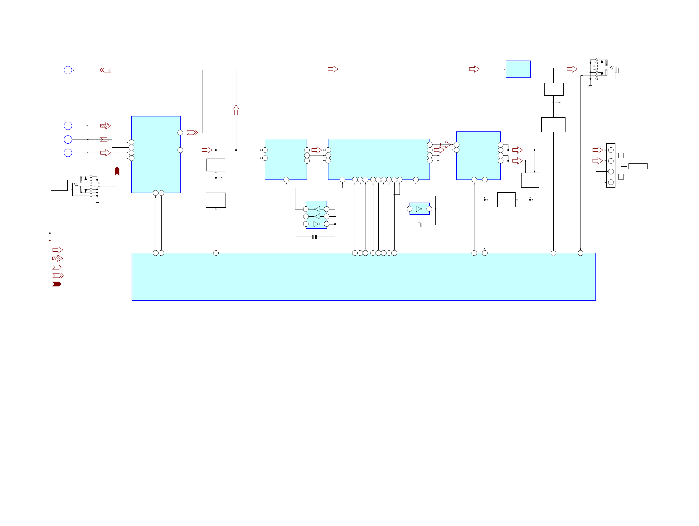
7-2. BLOCK DIAGRAM – MAIN Section –
HCD-CPZ1
J981
IN
D
B
C
A
TAPE REC-L
CD-L
TAPE PB-L
TUNER-L
(Page 20)
(Page 20)
(Page 20)
(Page 20)
ANALOG
R-ch is omitted due to same as L-ch.
Signal Path
: TUNER
: CD PLAY
: TAPE PLAY
: TAPE REC
: AUX IN
R-CH
INPUT SELECT,
ELECTRICAL VOLUME
7
B1
5
A1
9
C1
11
D1
IC501
18
51 50
SI
SC
17
AMP SI
AMP SC
SEL1
OUT1
HEADPHONE
AMP
IC502
MUTING
Q414
R-CH
MUTING
CONTROL
Q403, 404
53
HP MUTE
POWER DRIVER
2
22
MUTING
Q413
MUTING
CONTROL
Q401, 402
52
LINE MUTE
R-CH
R-CH
A/D CONVERTER
1
LIN
2
RIN
IC701
DOUT
LRCK
SCKI
15
12
BCK
11
10
OSC BUFFER
IC703
5 3
7
6
X701
12.288MHz
SYSTEM CONTROLLER
IC301 (2/3)
31
DATA
30
BCK
29
LRCK
36
1
2
XFSIIN
21
44
STREAM PROCESSOR
IC705
SCDT
SCSHIFT
SCLATCH
NSPMUTE
INIT
22
23
18
27
43
42
41
40
S-MASTER INIT
S-MASTER DATA
S-MASTER SHIFT
S-MASTER LATCH
S-MASTER NSP MUTE
SOFTMUTE
PGMUTE
OVF FLAGL24OVF FLAGR
19
20
25
47
48
49
S-MASTER OVF
S-MASTER PG MUTE
S-MASTER SOFT MUTE
OUTL1
OUTL2
OUTR1
OUTR2
XFSOIN
48
2 4
X702
49.152MHz
11
9
6
4
R-CH
R-CH
OSC
BUFFER
IC709
17
IC707
2
BP
AP
OUTA
OUTA
OUTB
OUTB
/RST
/SD
4
13
46
45
S-MASTER SD
S-MASTER RST
25
26
29
30
PROTECT
DETECT
Q701
DC
DETECT
Q702, 703
R-CH
R-CH
R-CH
R-CH
54
HP DET
J982
PHONES
+
L
–
+
J860
SPEAKER
R
–
HCD-CPZ1
2121
HCD-CPZ1
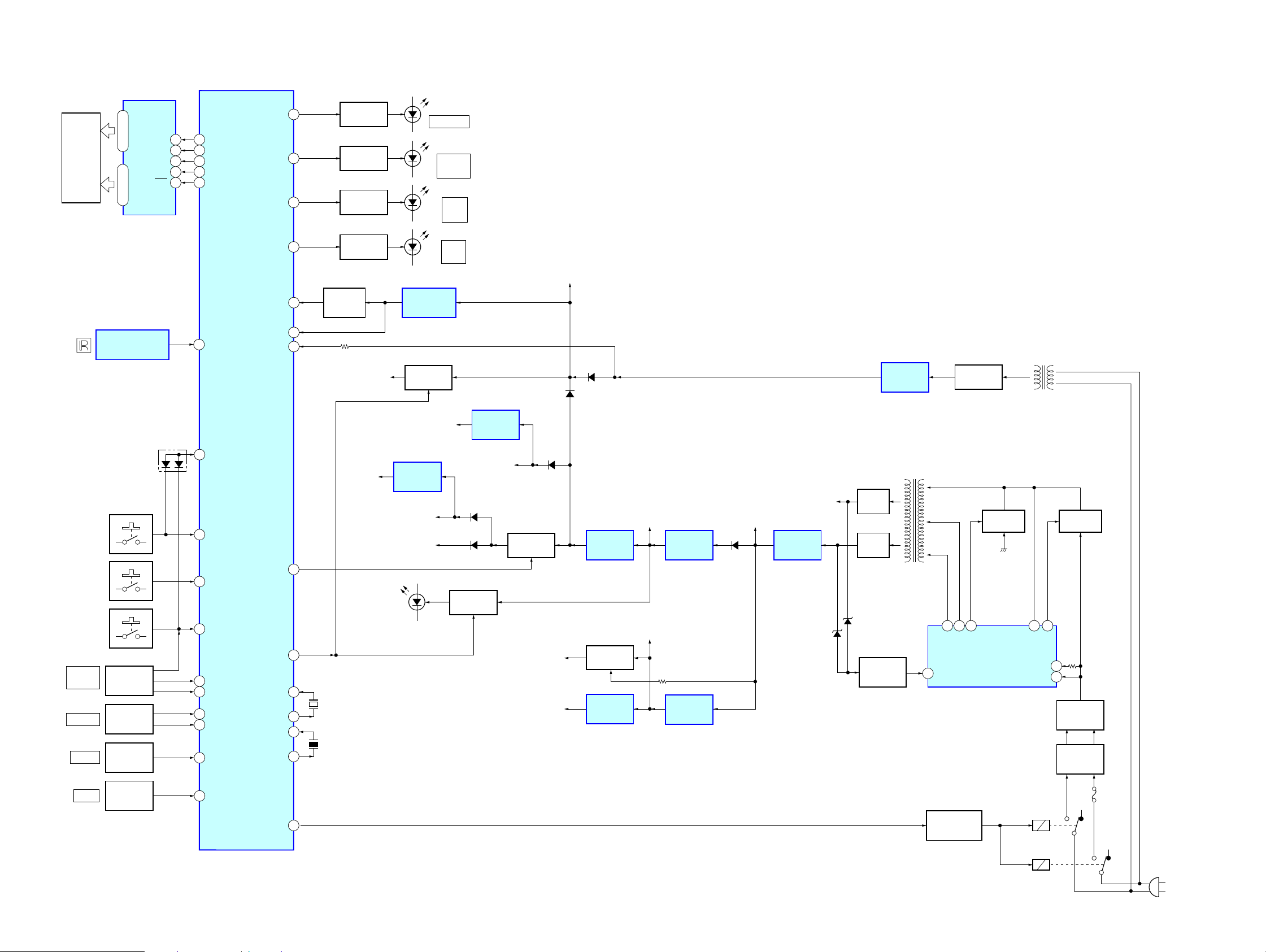
7-3. BLOCK DIAGRAM – PANEL/KEY/POWER SUPPLY Section –
LCD DRIVER
IC951
LED DRIVE
LED DRIVE
LED DRIVE
LIQUID
CRYSTAL
DISPLAY
LCD951
SEG1 – SEG37
64-61 1-37
COM1 – COM4
DATA
SCL
MODE
INH
LED STAND BY
59 LCD DATA
58
60 LCD SCL
57
56
59
60
61 LCD CE
58 LCD MODE
57 LCD INH
CE
LED TUNER
LED TAPE
72
66
65
Q901
Q902
Q903
D901
STANDBY
D902
TUNER
BAND
D903
TAPE
Y
S901 – 906
S907 – 912
S913 – 919
PUSH
ENTER
(JOG)
VOLUME
TREBLE
REMOTE CONTROL
RECEIVER
IC901
D303
ROTARY
ENCODER
RV904
ROTARY
ENCODER
RV903
ROTARY
ENCODER
RV902
4 SIRCS
SYSTEM CONTROLLER
IC301 (3/3)
74 WAKE UP KEY
97 KEY0
95 KEY1
94 KEY2
70 VOLUME A
71 VOLUME B
68 VOLUME A
69 VOLUME B
89 TREBLE
LED CD
XCIN
XCOUT
XIN
XOUT
IC302
B+ SWITCH
Q409, 410
S-MASTER
+1.8V
D904
CD
u
REGULATOR
S-MASTER
D502
D501
LED DRIVE
Q411, 412
+1.8V
IC704
+3.3V
B+ SWITCH
HEADPHONE AMP
Q407, 408
ADC +5V
µ-COM +3.3V
D202
+9V
D301
D302
REGULATOR
B+ SWITCH
REGULATOR
+4V
IC202
Q450
+5V
IC204
+7V
+9V
+7V
REGULATOR
IC201
+9V
REGULATOR
IC203
D203 – 205
+12V
+12V
REGULATOR
IC200
+28V
D34
RECT
D32
RECT
D31
D33
ISOLATOR
REGULATOR
TRANSFORMER
PH11
+4V
IC991
MAIN POWER
T31
SUB POWER
TRANSFORMER
T991
RECT
D992 – 995
SWITCHING
Q11
12
8
9
VC1
OCP
VG (L)
2
F/B
POWER CONTROL
IC11
SWITCHING
Q11
16
15
VS
VG (H)
1VSENSE
18VD
RECT
D1
LINE FILTER
T1, 2
RESET
SWITCH
Q301
X301
32.768kHz
X302
16MHz
LED DRIVE
Q904
LCD +3.3V
D +2.5V
RESET SIGNAL
GENERATOR
+2.5V
REGULATOR
IC202
D +3.3V
A +3.3V
D951, 952
(LCD BACK LIGHT)
67
12RESET
20AC CUT
1AC DET
81CD POWER ON/OFF
56LCD ON/OFF
10
11
15
13
BASS
HCD-CPZ1
ROTARY
ENCODER
RV901
90 BASS
POWER RELAY ON/OFF
F1
100
RELAY DRIVE
Q991
RY990
RY991
AC IN
2222
HCD-CPZ1
AMP board
SP board
TUNER PACK (FM/AM)
SUB POWER board
SUB PANEL board
MAIN board
BD board
DRIVER board
LCD board
OPT board
HP/MD board
PANEL board
TC board
SW POWER board
Ver. 1.1
• Note for Printed Wiring Boards and Schematic Diagrams
Note on Printed Wiring Board:
• X : parts extracted from the component side.
• Y : parts extracted from the conductor side.
f
•
• : Pattern from the side which enables seeing.
(The other layers' patterns are not indicated.)
Caution:
Pattern face side: Parts on the pattern face side seen from
(Conductor Side) the pattern face are indicated.
Parts face side: Parts on the parts face side seen from
(Component Side) the parts face are indicated.
• Indication of transistor.
: internal component.
C
Q
B
E
Q
B
CE
These are omitted.
These are omitted.
Note on Schematic Diagram:
• All capacitors are in µF unless otherwise noted. (p: pF)
50 WV or less are not indicated except for electrolytics
and tantalums.
• All resistors are in Ω and 1/
specified.
• f : internal component.
• 2 : nonflammable resistor.
• 5 : fusible resistor.
• C : panel designation.
Note: The components identified by mark 0 or dotted line
with mark 0 are critical for safety.
Replace only with part number specified.
• A : B+ Line.
• Voltages and waveforms are dc with respect to ground
under no-signal (detuned) conditions.
– BD Board –
no mark : CD PLAY
– TC Board –
no mark : TAPE PLAY
(): TAPE REC
– Other Section –
no mark : TUNER
(): CD PLAY
〈〈 〉〉 : TAPE PLAY
{ }: TAPE REC
• Voltages are taken with a V OM (Input impedance 10 MΩ).
Voltage variations may be noted due to normal production tolerances.
• Waveforms are taken with a oscilloscope.
Voltage variations may be noted due to normal production tolerances.
• Circled numbers refer to waveforms.
• Signal path.
F : TUNER
E : TAPE PLAY
a : TAPE REC
J : CD PLAY (ANALOG)
c : CD PLAY (DIGITAL)
j : AUX IN
• Abbreviation
AUS: Australian model
EE : East European model
KR : Korean model
SP : Singapore model
4
W or less unless otherwise
• Circuit Boards Location
HCD-CPZ1
2323
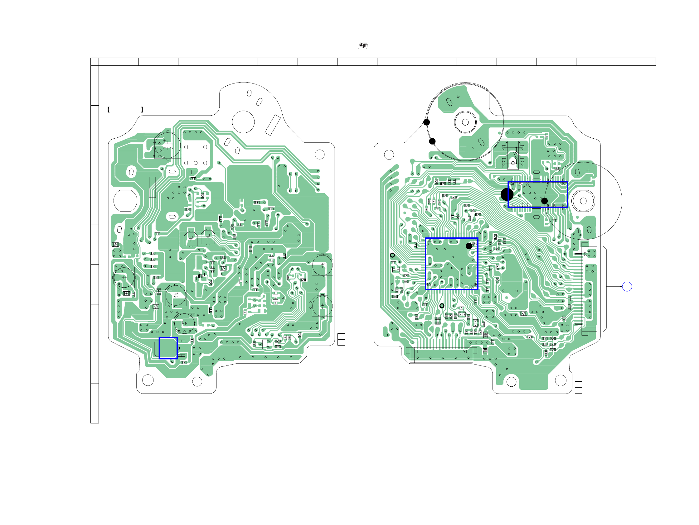
HCD-CPZ1
X201
C231
R256
C257
R260
C206
C205
C322
R323
R322
R321
R324
C223
C321
C268
C267
R271
R203
C226
R201
C227
C110
C108
C102
C203
C204
C270
C269
C101
R423
C202
R207
C215
R202
C201
C228
R421
C424
C210
Q321
C207
C275
C323
C406
R401
C401
C219
R276
C271
C104
C105
C107
C109
C232
C220
R249
R325
R326
M401
(SPINDLE)
M402
(SLED)
S201
(LIMIT)
C259
R257
C258
C260
C261
R258
R259
C208
R101
R265
R266
R267
C264
C265
R278
C111
C133
C214
R270
C221
C292
C291
R292
R291
C217
C132
C131
C218
C224
R451
R102
R103
R104
R105
R269
R107
R108
R110
R111
R279
C451
C256
C251
C252
C254
C253
R254
R255
R252
R253
CN301
C213
C222
C405
R113
C404
R452
C112
C452
R275
R277
C103
R112
C301
C302
C303
C273
R268
C113
CN102
C230
R250
R114
R272
R109
BD BOARD
(COMPONENT SIDE)
1-863-539-
11
(11)
TP
(VC)
TP
(RFACI)
1-863-539-
11
(11)
A
MAIN
BOARD
CN308
1 2 3 4 5 6 7 8 9 10 11 12 13 14
A
B
C
D
E
F
G
H
I
IC202
IC402
IC201
7-4. PRINTED WIRING BOARD – BD Section –
• See page 23 for Circuit Boards Location.
:Uses unleaded solder.
(Page 29)
HCD-CPZ1
2424
 Loading...