

Page 1
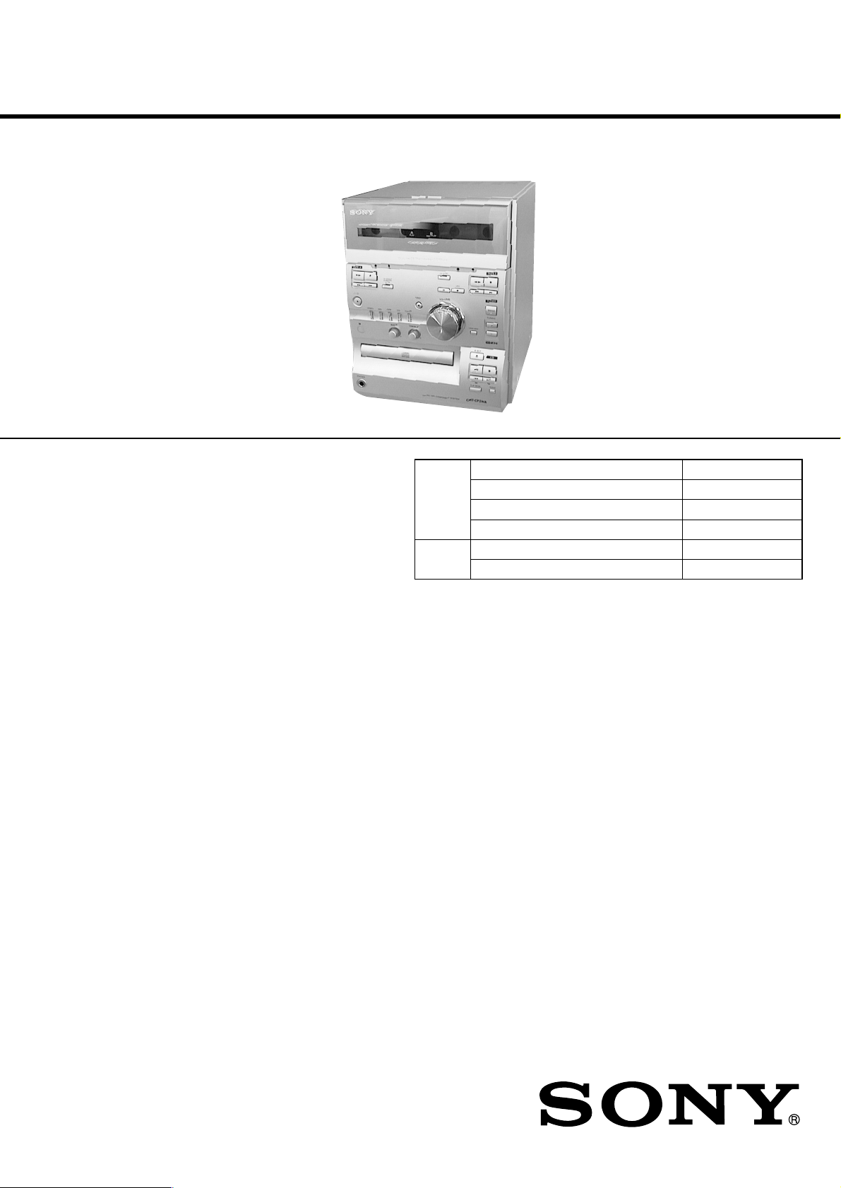
HCD-CP2A
SERVICE MANUAL
HCD-CP2A is the Amplifier, CD player,
Tape Deck and Tuner section in
CMT-CP2WA.
Dolby noise reduction manufactured under license
from Dolby Laboratories Licensing Corporation.
“DOLBY” and the double-D symbol ; are trademarks of Dolby Laboratories Licensing Corporation.
CD
Section
TAPE
Section
AEP Model
UK Model
E Model
Australian Model
Model Name Using Similar Mechanism NEW
CD Mechanism Type CDM55D-K5BD41
Base Unit Name BU-K5BD41
Optical Pick-up Name KSM-213CKP/K1N
Model Name Using Similar Mechanism NEW
Tape Transport Mechanism Type CMBL6Z112
SPECIFICATIONS
Amplifier section
European and Australian models:
DIN power output (rated): 30 + 30 W
Continuous RMS power output (reference):
Music power output (reference):
Other models:
The following measured at 230 V AC, 60 Hz
DIN power output (rated): 30 + 30 W
Continuous RMS power output (reference):
The following measured at 220 V AC, 60 Hz
DIN power output (rated): 28 + 28 W
Continuous RMS power output (reference):
Inputs
MD IN (phono jacks): Sensitivity 500 mV, impedance
VIDEO IN (phono jacks): Sensitivity 250 mV, impedance
Outputs
LINE OUT (phono jacks): Sensitivity 250 mV, impedance
OPTICAL DIGITAL OUT CD:
PHONES (stereo phone jack):
SPEAKER: Active speaker system, 6 ohms
(6 ohms at 1 kHz, DIN)
35 + 35 W
(6 ohms at 1 kHz, 10% THD)
130 W
(6 ohms at 1 kHz, DIN)
35 + 35 W
(6 ohms at 1 kHz, 10% THD)
(6 ohms at 1 kHz, DIN)
33 + 33 W
(6 ohms at 1 kHz, 10% THD)
47 kilohms
47 kilohms
1 kilohm
Optical
Accepts headphones with an
impedance of 8 ohms or more
CD player section
System Compact disc and digital audio
Laser Semiconductor laser
Laser output MAX 44.6
Wavelength 780 - 790 nm
Frequency response 20 Hz - 20 kHz (±0.5 dB)
Tape player section
Recording system 4-track 2-channel stereo
Frequency response (DOLBY NR OFF)
system
(λ = 780 nm)
Emission duration: continuous
µ
W*
* This output is the value
measured at a distance of
200 mm from the objective
lens surface on the Optical
Pick-up Block with 7 mm
aperture.
50 - 13,000 Hz (±3 dB), using a
Sony TYPE I cassette
50 - 14,000 Hz (±3 dB),
using a Sony TYPE II cassette
– Continued on next page –
COMPACT DISC DECK RECEIVER
Page 2

Tuner section
FM stereo, FM/AM superheterodyne tuner
FM tuner section
Tuning range 87.5 - 108.0 MHz
Antenna FM wire antenna
Antenna terminals 75 ohm unbalanced
Intermediate frequency 10.7 MHz
AM tuner section
Tuning range
European and Australian models:
Other models: 530 - 1,710 kHz
Antenna AM loop antenna, external antenna
Intermediate frequency 450 kHz
(50-kHz step)
531 - 1,602 kHz
(with the tuning interval set at
9 kHz)
(with the tuning interval set at
10 kHz)
531 - 1,602 kHz
(with the tuning interval set at
9 kHz)
terminal
TABLE OF CONTENTS
1. SERVICING NOTES ............................................... 3
2. GENERAL
Location of Controls ....................................................... 4
Setting the Time .............................................................. 5
Parts Identification for the Remote................................. 5
3. DISASSEMBLY ......................................................... 6
4. TEST MODE.............................................................. 10
5. MECHANICAL ADJUSTMENTS ....................... 11
6. ELECTRICAL ADJUSTMENTS
Tape Deck Section .......................................................... 11
CD Section ...................................................................... 14
General
Power requirements
European and Australian models:
Other models: 110 - 120 V or 220 - 240 V AC ,
Power consumption 70 W
Dimensions (w/h/d) Approx. 225 × 273 × 337 mm
Mass Approx. 6.7 kg
Design and specifications are subject to change
without notice.
230 V AC, 50/60 Hz
50/60 Hz
Adjustable with voltage selector
7
/8 × 10 3/4 × 13 3/8 in) incl.
(8
projecting parts and controls
(14 lb 12 oz)
7. DIAGRAMS
7-1. Note for Printed Wiring Boards and
Schematic Diagrams ....................................................... 15
7-2. Printed Wiring Board – CD Board – .............................. 16
7-3. Schematic Diagram – CD Section – ............................... 17
7-4. Printed Wiring Board – TC Board – ............................... 18
7-5. Schematic Diagram – TC Section – ............................... 19
7-6. Schematic Diagram – MAIN Section (1/3) –................. 20
7-7. Schematic Diagram – MAIN Section (2/3) –................. 21
7-8. Schematic Diagram – MAIN Section (3/3) –................. 22
7-9. Printed Wiring Board – MAIN Board – ......................... 23
7-10. Printed Wiring Board – LOADING Board –.................. 24
7-11. Printed Wiring Board – LCD Board – ............................ 24
7-12. Printed Wiring Boards
– AMP/HEADPHONE Boards – .................................... 24
7-13. Sc hematic Dia gram – AMP Section – ............................ 25
7-14. Printed Wiring Board – CONTROL Board – ................. 26
7-15. Sc hematic Diagram – CONTROL Section –.................. 27
7-16. Printed Wiring Board – POWER Board – ...................... 28
7-17. Sc hematic Dia gram – POWER Section – ...................... 28
7-18. IC Pin Function Description ........................................... 35
8. EXPLODED VIEWS ................................................ 38
9. ELECTRICAL PARTS LIST ............................... 43
SAFETY-RELATED COMPONENT WARNING!!
COMPONENTS IDENTIFIED BY MARK 0 OR DOTTED
LINE WITH MARK 0 ON THE SCHEMATIC DIAGRAMS
AND IN THE PARTS LIST ARE CRITICAL TO SAFE
OPERATION. REPLACE THESE COMPONENTS WITH
SONY PARTS WHOSE PART NUMBERS APPEAR AS
SHOWN IN THIS MANU AL OR IN SUPPLEMENTS PUBLISHED BY SONY.
2
Page 3
SECTION 1
SERVICING NOTES
Notes on chip component replacement
• Never reuse a disconnected chip component.
• Notice that the minus side of a tantalum capacitor may be damaged by heat.
Flexible Circuit Board Repairing
• Keep the temperature of the soldering iron around 270 ˚C during repairing.
• Do not touch the soldering iron on the same conductor of the
circuit board (within 3 times).
• Be careful not to apply force on the conductor when soldering
or unsoldering.
CAUTION
Use of controls or adjustments or performance of procedures
other than those specified herein may result in hazardous radiation exposure.
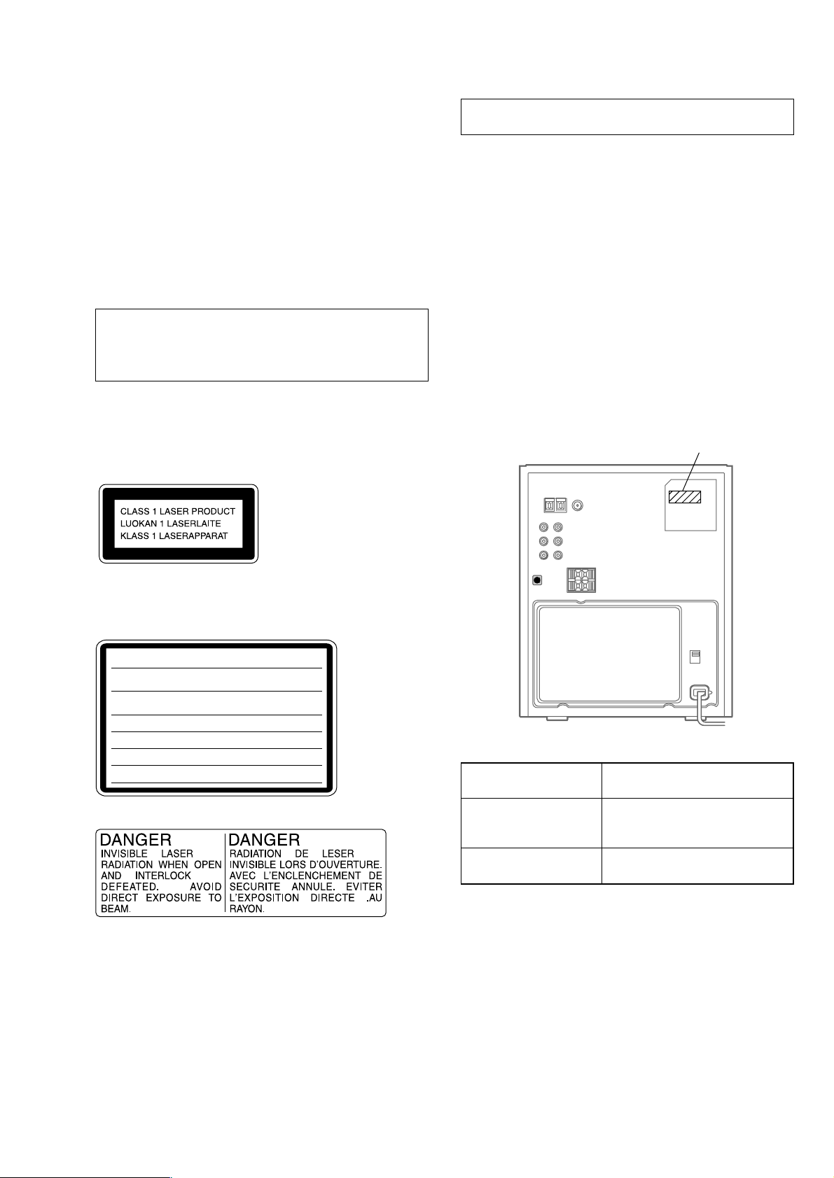
This appliance is classified as a CLASS 1 LASER product.
The CLASS 1 LASER PRODUCT MARKING is located on
the rear exterior.
NOTES ON HANDLING THE OPTICAL PICK-UP
BLOCK OR BASE UNIT
The laser diode in the optical pick-up block may suffer electrostatic break-down because of the potential difference generated
by the charged electrostatic load, etc. on clothing and the human
body.
During repair, pay attention to electrostatic break-down and also
use the procedure in the printed matter which is included in the
repair parts.
The flexible board is easily damaged and should be handled with
care.
NOTES ON LASER DIODE EMISSION CHECK
The laser beam on this model is concentrated so as to be focused
on the disc reflective surface by the objective lens in the optical
pick-up block. Therefore, when checking the laser diode emission, observe from more than 30 cm away from the objective lens.
• MODEL IDENTIFICATION
– Rear Panel –
Power Voltage Indication
Laser component in this product is capable of emitting radiation
exceeding the limit for Class 1.
The following caution label is located inside the unit.
CAUTION :
INTERLOCKS DEFEATED. AVOID EXPOSURE TO BEAM.
ADVARSEL :
SIKKERHEDSAFBRYDERE ER UDE AF FUNKTION. UNDGÅ UDSAETTELSE
FOR STRÅLING.
VORSICHT :
ABDECKUNG GEÖFFNET UND SICHEREITSVERRIEGELUNG
ÜBERBRÜCKT. NICHT DEM STRAHL AUSSETZEN.
VARO! :
TIINA NÄKYMÄTTÖMÄLLE LASERSÄTEILYLLE. ÄLÄ KATSO SÄTEESEEN.
VARNING :
OCH SPÄRREN ÄR URKOPPLAD. BETRAKTA EJ STRÅLEN.
ADVERSEL :
SIKKERHEDSLÅS BRYTES. UNNGÅ EKSPONERING FOR STRÅLEN.
VIGYAZAT! :
GÁRVESZÉLY! KERÜLJE A BESUGÁRZÁST!
INVISIBLE LASER RADIATION WHEN OPEN AND
USYNLIG LASERSTRÅLING VED ÅBNING NÅR
UNSICHTBARE LASERSTRAHLUNG, WENN
AVATTAESSA JA SUOJALUKITUS OHITETTAESSA OLET ALT -
OSYNLING LASERSTRÅLING NÄR DENNA DEL ÄR ÖPPNAD
USYNLIG LASERSTRÅLING NÅR DEKSEL ÅPNES OG
A BURKOLAT NYITÁSAKOR LÁTHATATLAN LÉZERSU-
Model Power V oltage Indication
AEP, UK,
North European and AC: 230 V -50/60 Hz 70 W
Australian models
Saudi Arabia
AC: 110 – 120/220 – 240 V
-50/60 Hz 70 W
3
Page 4
• LOCATION OF CONTROLS
– Front View –
123
qf
qg
b B x
mM
qh
qj
qk
w;ql
Xz
b B x
mM
+
–
Z
x
u
.>
M
m
SECTION 2
GENERAL
4
5
6
7
8
9
q;
qa
qs
qd
1 TAPE A deck
2 TAPE B deck
3 Liquid crystal display
4 TAPE B Y button
5 TAPE B x button
6 TAPE B M button
7 TAPE B m button
8 VOLUME knob
9 TREBLE knob
0 BASS knob
qa CD EJECT Z button
qs CD REPEAT button
qd CD PLAY MODE button
qf TAPE A x button
qg TAPE A Y button
qh TAPE A m button
qj TAPE A M button
qk Remote control sensor
ql PHONES jack
w; CD disc tray
ed
wa ws wd wfwg
b B x
mM
wa HI-SPEED DUBBING AtB button and indicator
ws DSG button and indicator
wd X button (TAPE A/B)
wf CD SYNC button and indicator
wg REC button
wh TUNING MODE button
Xz
b B x
mM
wh
wj
+
–
wk
wj TUNER BAND button
wk TUNING +/– buttons
wl CD u button
e; CD x button
ea > M button
Z
x
u
.>
M
m
wl
e;
ea
es . m button
ed I/1 button and indicator
ef VIDEO button and indicator
eg MD button and indicator
es
ekejehegef
eh TAPE button and indicator
ej CD button and indicator
ek TUNER button and indicator
4
Page 5
This section is extracted from
6
Step 2: Setting the time
Before you can use the system’s timer functions,
set the internal clock.
The clock uses a 24-hour system on the European
model, and a 12-hour system on other models.
The 24-hour system is used here for illustration
purposes.
3,5
1
2,4
1
Press TIMER SET.
The hour indication flashes.
000
2
Press l/L repeatedly to set the
hour.
1300
3
Press ENTER.
The minute indication flashes.
1300
4
Press l/L repeatedly to set the
minute.
1310
5
Press ENTER.
The clock starts working.
To reset the system clock
You can reset the system clock when the system is
on.
1 Press TIMER SET.
2 Press l/L repeatedly until
“SET CLOCK” appears, then press ENTER.
3 Repeat step 2 to 5 in “Step 2: Setting the time”.
Tip
If you make a mistake, start over from step 1.
33
Additional Information
Parts identification for
the remote
You can also operate the system with the supplied
remote.
Buttons marked with
“*” are provided only on the
remote.
TUNER
Remote
Button(s)
Function
TUNER/BAND
Selects FM or AM.
CD
Remote
Button(s)
Function
CD H
s Stops playback.
S Pauses playback.
l/L Selects a track (AMS: Automatic
Music Sensor).
j/J Locates a desired point in a
track.
CD REPEAT Repeats playback.
TAPE
Remote
Button(s)
For operating
the
Function
TAPE A (or B)
nN
Deck A or B Starts playback.
Each time you
press this button,
the tape reverses
direction.
s Deck A or B Stops playback.
S Deck A or B Pauses playback.
j/J Deck A or B Fast-forwards or
rewinds.
z REC Deck B Records to tapes.
Remote
Button(s)
Function
?/1 Turns on or off the system.
VOL +/– Adjusts the volume.
FUNCTION Selects the source.
TUNING MODE Selects “AUTO”, “PRESET” or
“MANUAL”.
MEMORY* Presets a station.
STEREO/MONO* Selects “STEREO” or “MONO”.
l/L Selects a preset number.
j/J Scans for a station or selects a
preset station.
Starts playback.
PLAY MODE Selects Shuffle, Program or
Normal Play.
DISPLAY* Changes the front panel display.
DIR MODE* Deck A or B Selects “
”,
“
” or “R”.
DOLBY NR* Deck A or B Turns on or off the
Dolby NR system.
TIMER
Remote
Button(s)
Function
SLEEP* Selects a sleep time.
TIMER SET* Sets the time, Daily Timer or
REC Timer.
TIMER SELECT* Checks the settings and turns on
or off the timer.
OTHERS
DSG Generates a more dynamic
sound.
instruction manual.
5
Page 6
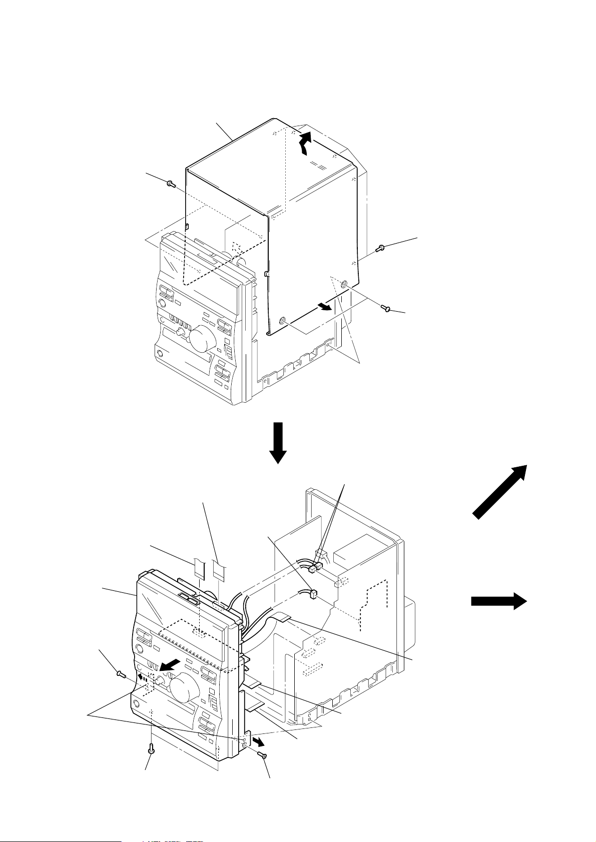
SECTION 3
s
DISASSEMBLY
Note: Follow the disassembly procedure in the numerical order given.
COVER (UPPER)
3 cover (upper)
1 two case screws
2 six screws
(BTP3 × 8)
1 two case screw
FRONT PANEL ASS’Y
1 wire (flat type)(14 core)
(CN401)
6 front panel ass’y
4 screw
(KTP3 × 6)
5 two bosses
1 wire (flat type)(17 core)(22 cm)
2 connector
(CN311)
2 two connectors
(CN805, 808)
1 wire (flat type)(21 core)
(CN803)
1 wire (flat type)(23 core)
(CN806)
1 wire (flat type)(FFC)(17 core)
(23 cm)(CN801)
3 two screws
(BTP3 × 8)
4 screw
(KTP3 × 6)
6
Page 7
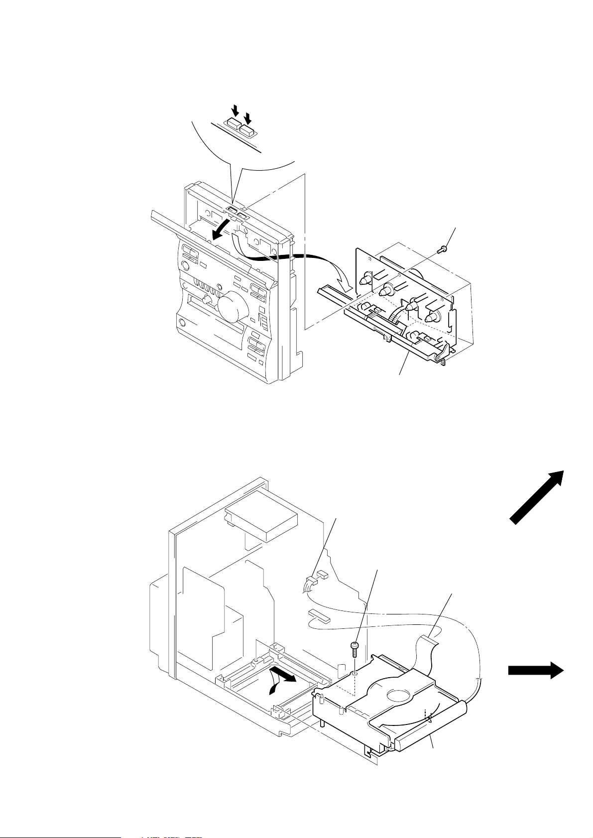
TAPE MECHANISM DECK SECTION
)
2 Push these buttons.
1 six screws
(BTP3 × 8
CD MECHANISM DECK (CDM55D-K5BD41)
3 tape mechanism deck section
2 connector
(CN304)
3 screw
(BTP3 × 8)
1 wire (flat type)(19 core)
(CN301)
4 CD mechanism deck
(CDM55D-K5BD41)
7
Page 8
BASE UNIT (BU-K5BD41)
2 base unit
(BU-K5BD41)
1 floating screw
(PTPWHM2.6)
TRAY, LOADING BOARD
3 Pull the tray pushing B.
2 belt (CDM55)
B
A
1 Rotate the gear(B) in
the direction of arrow A.
5 LOADING board
4 two screws
(BTP2.6 × 6)
8
Page 9
CAM (CDM55)
3 spacer (55)
4 pulley (LDG)
2 lever (SW)
1 torsion spring
6 gear (B)
5 gear (A)
7 roller
8 cam (CDM55)
9
Page 10
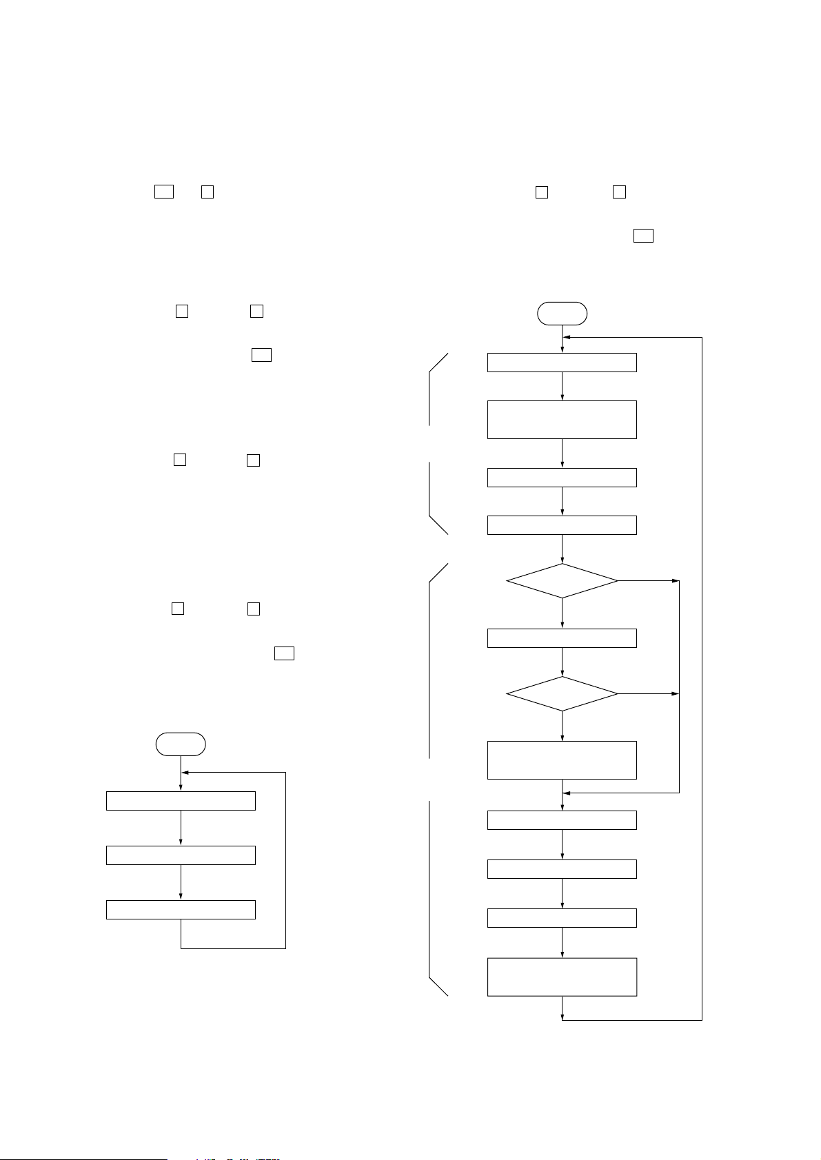
SECTION 4
TEST MODE
[MC Cold Reset]
• The cold reset clears all data including preset data stored in the
RAM to initial conditions. Execute this mode when returning
the set to the customer.
Procedure:
1. While pressing the I/1 and x (T APE A) button, connect the
power cord.
2. The set is reset.
[Liquid Crystal Display All Lit Check Mode]
Procedure:
1. Set to standby state.
2. Press thr ee buttons of x (TAPE B), x (CD), and [VIDEO]
(function) simultaneously.
3. Liquid crystal display are all turned on.
4. To release from this mode, press the I/1 button to turn the
power OFF.
[ROM Version Display Mode]
Procedure:
1. Set to standby state.
2. Press three buttons of x (TAPE B), x (CD), and [DSG] si-
multaneously.
3. The ROM version is displayed.
[Tape Deck Aging Mode]
This mode can be used for operation check of tape deck section.
Procedure:
1. Set tapes in the tape deck-A and B.
2. Set to standby state.
3. Press three buttons of x (TAPE B), x (CD), and [TAPE]
(function) simultaneously.
4. The aging is executed in bellow sequence.
5. To release from the aging mode, press the I/1 button to turn
the power OFF.
Aging mode sequence:
Start
FWD play for 2 minutes *1
Fast forward for
20 seconds or till shut off
TAPE A
REV play for 3 minutes
[CD Aging Mode]
This mode can be used for operation check of CD section.
Procedure:
1. Load a CD disc.
2. Set to standby state.
3. Press three buttons of x (TAPE B), x (CD), and [TUNER]
(function) simultaneously.
4. T he aging is executed in bellow sequence.
5. To release from the aging mode, press the I/1 button to turn
the power OFF.
Aging mode sequence:
Start
Open the disc tray
Close the disc tray
Play the last track
TAPE B
Rewind for 10 seconds
FWD Play
1 minute
REC pause for 3 seconds
FWD REC
3 minutes
Fast forward for
20 seconds or till shut off
REV play for 1 minute
REC pause for 3 seconds
REV REC for 3 minutes
Shut off
Shut off
10
Rewind for 30 seconds
or till shut off
*1) When it shuts off within 2 minutes, it
REV plays rest of the time then goes
to the next step.
Page 11
SECTION 5
MECHANICAL ADJUSTMENTS
SECTION 6
ELECTRICAL ADJUSTMENTS
PRECAUTION
1. Clean the following parts with a denatured-alcohol-moistened
swab:
record/playback heads pinch rollers
erase head rubber belts
capstan idlers
2. Demagnetize the record/playback head with a head demagnetizer.
3. Do not use a ma gnetized screwdriver for the adjustments.
4. After the adjustments, apply suitable locking compound to
the parts adjusted.
5. T he adjustments should be performed with the rated power
supply voltage unless otherwise noted.
• Torque Measurement
• Tape Tension Measurement
• Tor que Measurement
Mode Torque Meter Meter Reading
Forward CQ-102C 36 to 61 g•cm
Forward
Back Tension
Reverse CQ-102RC 36 to 61 g•cm
Reverse
Back Tension
FF, REW CQ-201B 61 to 143 g•cm
CQ-102C 2 to 6 g•cm
CQ-102RC 2 to 6 g•cm
3.53 ~ 5.98 mN•m
(0.50 – 0.84 oz•inch)
0.20 ~ 0.58 mN•m
(0.026 – 0.082 oz•inch)
3.53 ~ 5.98 mN•m
(0.50 – 0.84 oz•inch)
0.20 ~ 0.58 mN•m
(0.026 – 0.082 oz•inch)
5.99 ~ 14.02 mN•m
(0.85 – 1.98 oz•inch)
• T ape Tension Measurement
Mode Tension Meter Meter Reading
Forward CQ-403A
Reverse CQ-403R
more than 9.8 N
more than 100 g (3.52 oz)
more than 9.8 N
more than 100 g (3.52 oz)
0 dB=0.775 VTAPE DECK SECTION
1. Demagnetize the record/playback head with a head demagnetizer. (Do not bring the head demagnetizer close to the erase
head)
2. Do not use a magnetized screwdriver for the adjustments.
3. After the adjustments, apply suitable locking compound to
the parts adjust.
4. The adjustments should be performed with the rated power
supply voltage unless otherwise noted.
5. The adjustments should be performed in the order given in
this service manual. (As a general rule, playback circuit adjustment should be completed before performing recording
circuit adjustment)
6. The adjustments should be performed for both L-CH and Rch.
7. Switches and controls should be set as follows unless otherwise specified.
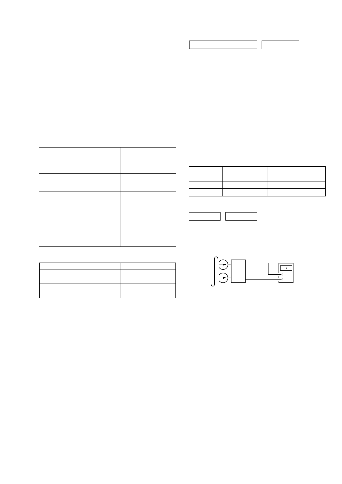
• Test T ape
Tape Signal Used for
P-4-A100 10 kHz, –10 dB Azimuth Adjustment
WS-48B 3 kHz, 0 dB Tape Speed Check
P-4-L300 315 Hz, 0 dB Level Adjustment
Record/ Playback Head Azimuth Adjustment
DECK A DECK B
Note: Perform this adjustments for both decks
Procedure:
test tape
P-4-A100
(10 kHz, –10 dB)
set
MAIN board
IC306
Pin r; (L-CH)
Pin 3 (R-CH)
MAIN board
IC306
Pin rl
level meter
+
–
11
Page 12
(
)
(
)
1. Mode: Playback (FWD)
e
2. Turn the adjustment screw and check output peaks. If the peaks
do not match for L-CH and R-CH, turn the adjustment screw
so that outputs match within 1dB of peak.
Tape Speed Check
Procedure:
Mode: Playback (FWD)
test tape
WS-48B
(3 kHz, 0 dB)
DECK A DECK B
frequency counter
within
output
level
1dB
L-CH
peak
R-CH
peak
within
1dB
Screw
position
L-CH
peak
Screw
position
R-CH
peak
3. Mode: Playback (FWD)
test tape
P-4-A100
(10 kHz, –10 dB)
L-CH
MAIN
board
IC401
set
R-CH
waveform of oscilloscope
in phase 45 °
pin r;
pin rl
L
R
pin
3
90 ° 135 ° 180 °
good
oscilloscope
V
wrong
H
4. Repeat steps 1 to 3 in playback (REV) mode.
5. After the adjustments, apply suitable locking compound to the
pats adjusted.
Adjustment Location: Record/Playback Head (Deck A and B)
and MAIN board.
set
MAIN board
IC306(Pin r; : L-CH)
Pin 3 : R-CH
+
–
1. Insert the WS-48B into the deck A and the blank tape into the
deck B.
2. Press the [HI-SPEED DUBBING] button and X button.
Then at HIGH speed dubbing.
3. Check that frequency counter reads 6,000 ± 180 Hz.
4. Press the x (TAPE A or B) button to stop the HIGH speed
dubbing.
5. Press the [REC ], X and Y button.
z
Then at NORMAL speed dubbing.
6. Check that frequency counter reads 3,000 ± 90 Hz.
7. Press the
x (T APE A or B) button to stop the NORMAL speed
dubbing.
8. Frequency difference between deck A and deck B the beginning of the tape should be within ± 1.5%.
Checking Location: MAIN board
Sample Value of Wow and flutter: 0.3% or less W. RMS (JIS)
(WS-48B)
Playback level Adjustment
DECK A DECK B
Procedure:
Mode: Playback (FWD)
test tape
P-4-L300
(315 Hz, 0 dB)
set
MAIN board
IC306 (Pin r; : L-CH)
level meter
+
–
Pin 3 : R-CH
12
forward
Deck A is RV401 (L-CH) and RV421 (R-CH), Deck B is RV402
(L-CH) and RV422 (R-CH) on the TC board so that adjustment
within adjustment level as follows.
Adjustment Level:
revers
IC306 PB level: 301.5 to 338.3 mV (–8.2 to –7.2 dB) level
difference between the channels: within ± 0.5 dB
Adjustment Location: TC and MAIN boards
Page 13
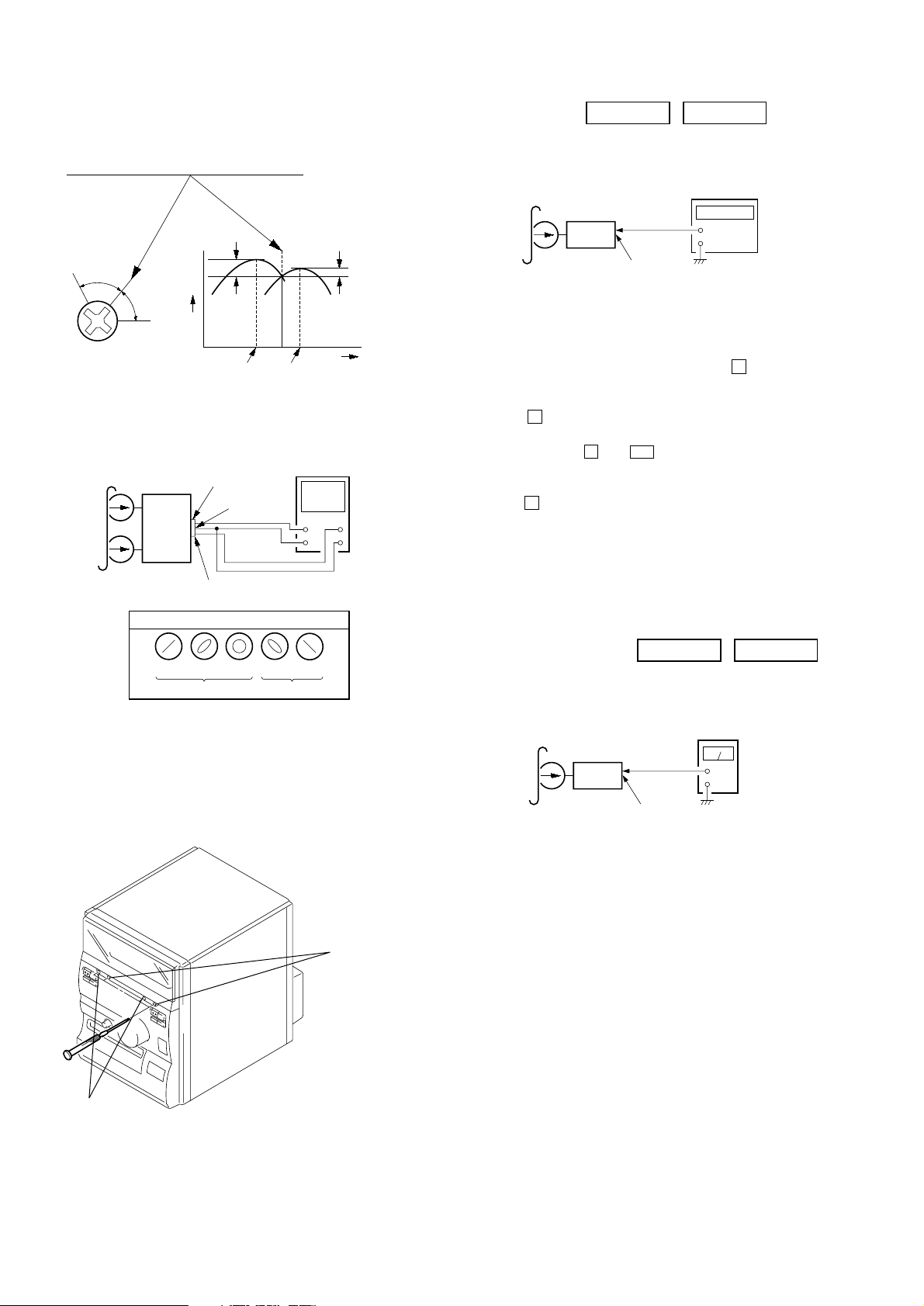
Record bias Current Adjustment
(
)
(
)
Procedure:
1. Mode: Record
Pin rd (L-CH) of IC306 on the MAIN board.
Pin th (R-CH) of IC306 on the MAIN board.
1) 315 Hz
2) 10 kHz
AF OSC
attenuator
Pin rl (GND) of IC306 on the MAIN
board.
50 mV (–23.8 dB)
600 Ω
2. Mode: Playback
recorded
portion
set
DECK B
set
level meter
+
–
blank tape
CN-123
Adjustment and Checking Location:
– MAIN BOARD (Conductor Side) –
Record Level (R)
Record Level (L)
49
RV201
3
RV101
40
IC306
IC306 (Pin r; : L-CH)
Pin 3 : R-CH
Confirm playback the signal recorded in step 1 become adjustable
limits as follows.
If these levels do not adjustable limits, adjustment the RV403 (LCH) and RV423 (R-CH) on the TC board to repeat steps 1 and 2.
Adjustable limits: Playback output of 315 Hz to playback output
of 10 kHz: 0 ± 0.5 dB
Adjustment Location: TC and MAIN boards
Record Level Adjustment
DECK B
Procedure:
1. Mode: Record
Pin rd (L-CH) of IC306 on the MAIN board.
Pin
th (R-CH) of IC306 on the MAIN board.
AF OSC
315 Hz, 50 mV (–23.8 dB)
attenuator
Pin
rl (GND) of IC306 on the MAIN board.
600 Ω
set
blank tape
CS-123
2. Mode: Playback
– TC BOARD (Component Side) –
Playback Level
(Deck-A)
LL LRR R
RV401 RV421 RV402 RV422
Playback Level
(Deck-B)
Record Bias
Current
RV403
RV423
recorded
portion
set
IC306 (Pin r; : L-CH)
level meter
+
–
Pin 3 : R-CH
Confirm playback the signal recorded in step 1 become adjustable
limits as follows.
If these levels do not adjustable limits, adjustment the RV101 (LCH) and R V201 (R-CH) on the MAIN board to repeat steps 1 and
2.
Adjustable limits:
IC306 PB level: 36.7 to 41.1 mV (–26.5 to –25.5 dB)
Adjustment Location: MAIN board
13
Page 14
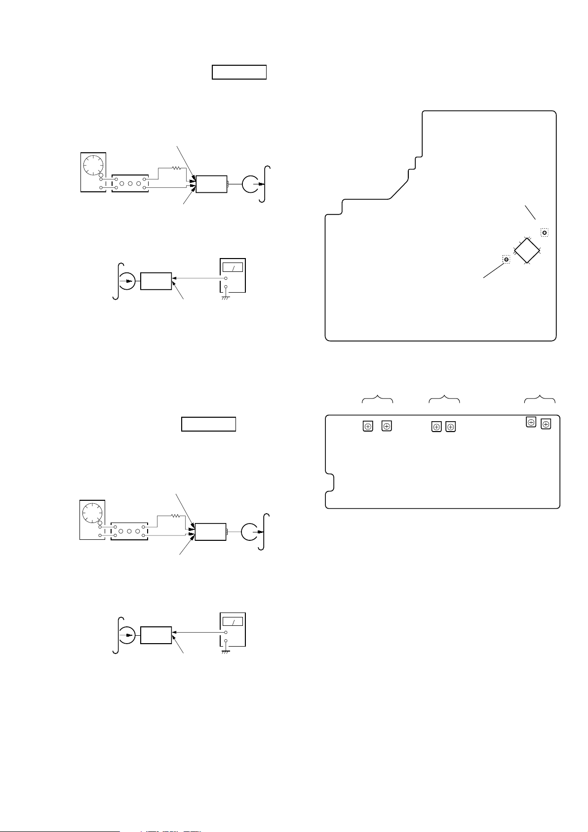
CD SECTION
V
Note:
1. CD Block is basically constructed to operate without
adjustment.
2. Use YEDS-18 disc (3-702-101-01) unless otherwise indicated.
3. Use an oscilloscope with more than 10 MΩ impedance.
4. Clean the object lens by an applicator with neutral detergent
when the signal level is low than specified value with the
following checks.
5. Check the focus bias check when optical block is replaced.
Focus Bias Check
oscilloscope
(DC range)
BD board
– CD BOARD (Conductor Side) –
TP (RF)
TP (VC)
+
–
Procedure :
1. Connect oscilloscope to TP (RF) and TP (VC) on the CD board.
2. Press the I/1 button to turn the power on, and press the Z
(CD) button to open the CD disc tray.
3. Put disc (YEDS-18) in and press the u (CD) button to playback.
4. Confirm that oscilloscope waveform is as shown in the figure
below. (eye pattern)
A good eye pattern means that the diamond shape ( ) in the
s
center of the waveform can be clearly distinguished.
VOLT/DIV: 200 m
TIME/DIV: 500 ns
level:
1.2 ± 0.1 Vp-p
Checking Location:
IC103
TP (RF)
TP (VC)
14
Page 15
SECTION 7
POWER board
LCD board
TC board
CONTROL board
HEADPHONE board
LOADING board
CD board
MAIN board
AMP board
TUNER PACK (TCB-020)(AEP, UK, Australian)
TUNER PACK (TCB-020N)(Saudi Arabia)
DIAGRAMS
HCD-CP2A
7-1. NOTE FOR PRINTED WIRING BOARDS AND SCHEMATIC DIAGRAMS
Note on Printed Wiring Boards:
• X : parts extracted from the component side.
• Y : parts extracted from the conductor side.
• W : indicates side identified with part number.
• b : Pattern from the side which enables seeing.
• Abbreviation
AUS : Australian model
EA : Saudi Arabia model
Note on Schematic Diagram:
• All capacitors are in µF unless otherwise noted. pF: µµF
50 WV or less are not indicated except for electrolytics
and tantalums.
• All resistors are in Ω and 1/
specified.
f
•
• C : panel designation.
Note: The components identified by mark 0 or dotted line
• U : B+ Line.
• V : B– Line.
• H : adjustment for repair.
• V oltages are taken with a VOM (Input impedance 10 MΩ).
• Waveforms are taken with a oscilloscope.
• Circled numbers refer to waveforms.
• Signal path.
• Abbreviation
: internal component.
with mark 0 are critical for safety.
Replace only with part number specified.
Voltage variations may be noted due to normal production tolerances.
Voltage variations may be noted due to normal production tolerances.
F : TUNER
E : TAPE PLAY (DECK A)
d : TAPE PLAY (DECK B)
G : TAPE REC
J : CD PLAY (ANALOG)
c : CD PLAY (DIGITAL)
AUS : Australian model
EA : Saudi Arabia model
4
• Circuit Boards Location
W or less unless otherwise
1515
Page 16
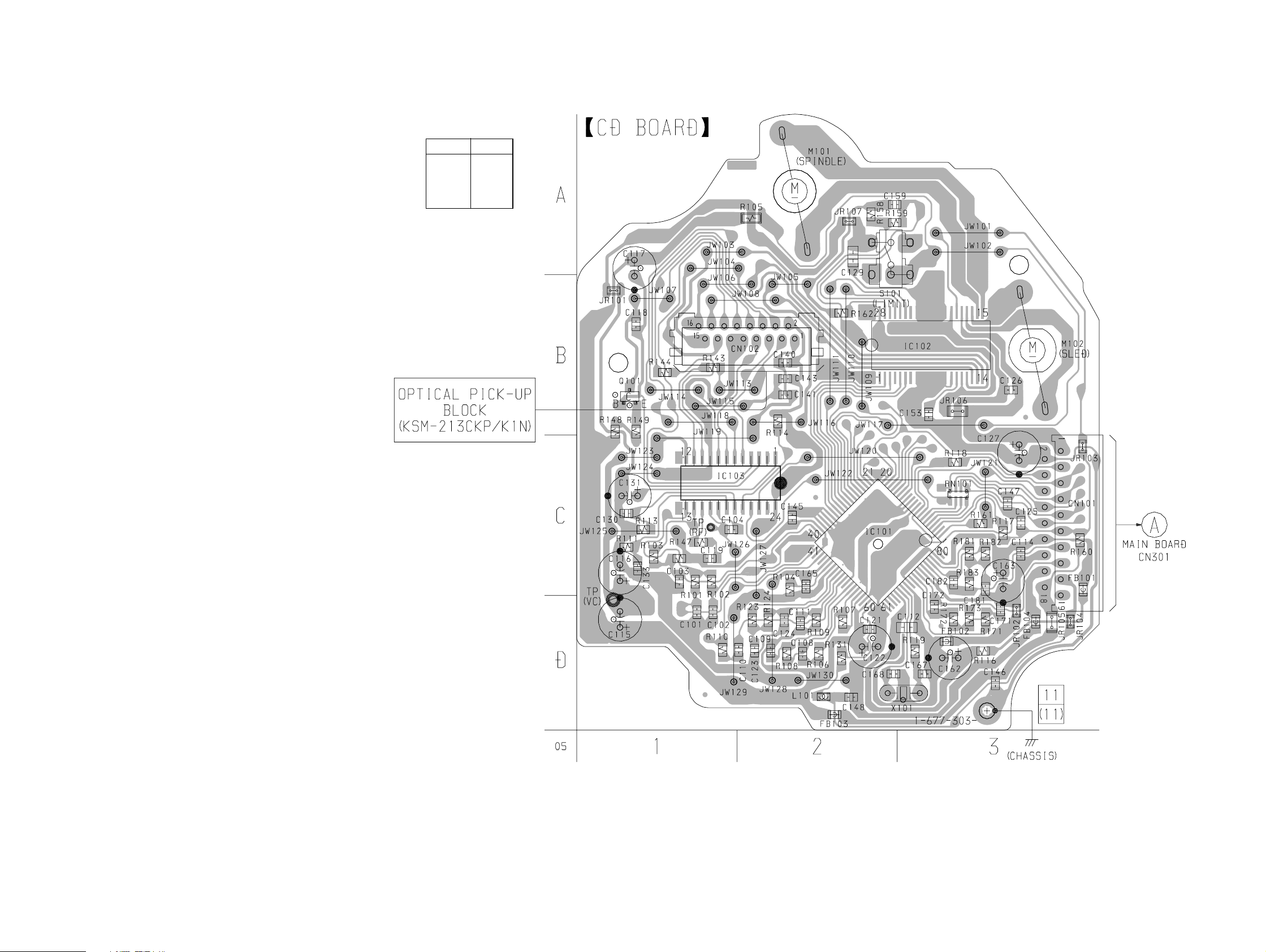
HCD-CP2A
7-2. PRINTED WIRING BOARD – CD Board – • See page 15 for Circuit Boards Location.
• Semiconductor
Location
Ref. No. Location
IC101 C-2
IC102 B-3
IC103 C-2
Q101 B-1
(Page 23)
1616
Page 17
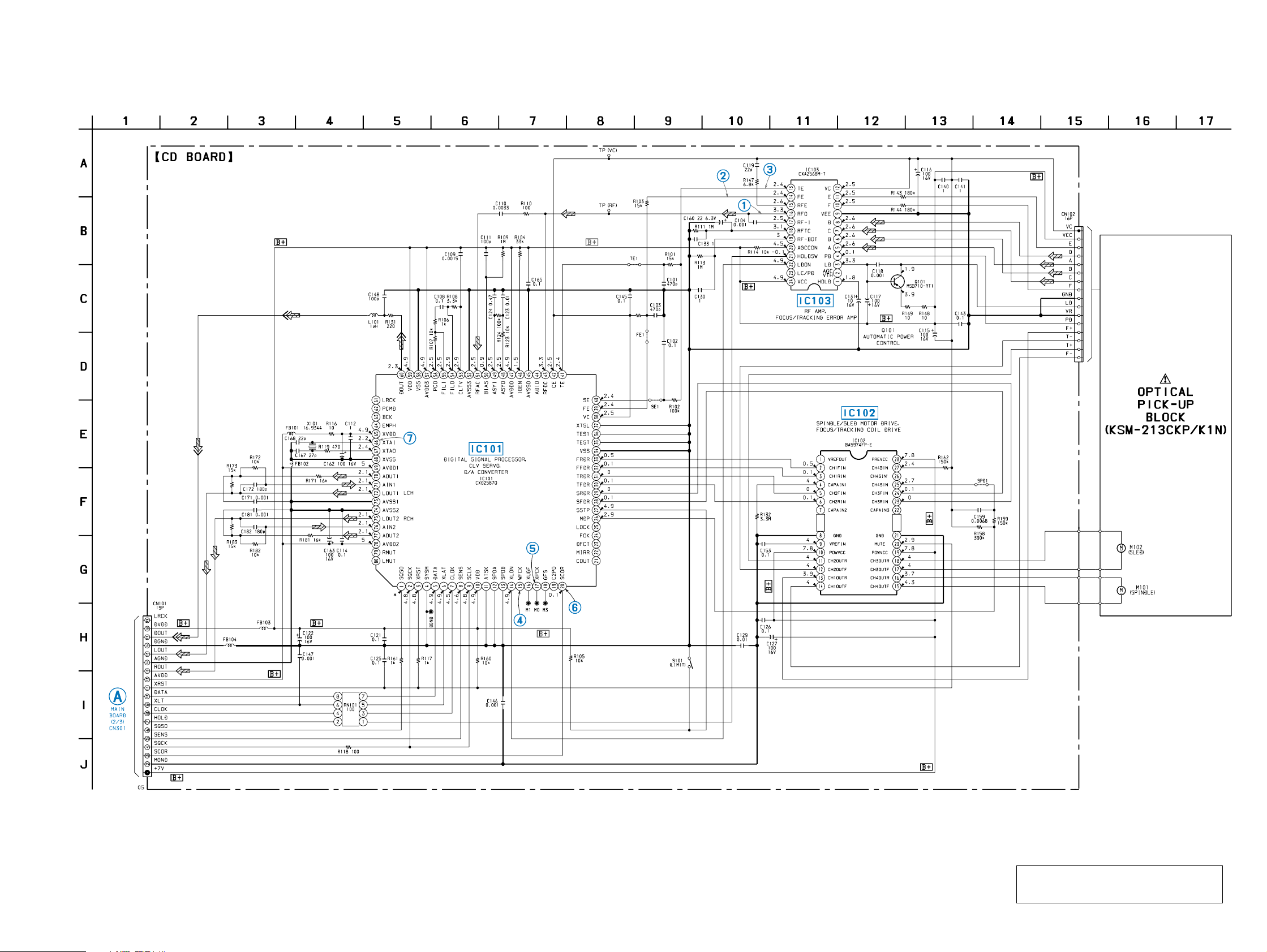
7-3. SCHEMATIC DIAGRAM – CD Section – • See page 29 for Waveforms. • See page 31 for IC Block Diagrams.
HCD-CP2A
(Page 21)
• Voltages and waveforms are dc with respect to ground
under no-signal conditions.
no mark : CD PLAY
The components identified by mark 0 or dotted
line with mark 0 are critical for safety.
Replace only with part number specified.
: Impossible to measure
∗
1717
Page 18

HCD-CP2A
7-4. PRINTED WIRING BOARD – TC Board – • See page 15 for Circuit Boards Location.
(Page 23)
• Semiconductor
Location
Ref. No. Location
IC401 B-6
IC402 B-2
IC403 B-2
Q401 B-2
Q402 B-1
Q403 A-2
Q404 A-2
1818
Page 19

7-5. SCHEMATIC DIAGRAM – TC Section – • See page 29 for Waveforms.
HCD-CP2A
(Page 20)
• Voltages and waveforms are dc with respect to ground
under no-signal conditions.
no mark : TAPE PLAY
〈〈 〉〉 : TAPE REC
1919
Page 20

HCD-CP2A
7-6. SCHEMATIC DIAGRAM – MAIN Section (1/3) –
(Page 19)
(Page 21)
(Page 22)
• Voltages and waveforms are dc with respect to ground
under no-signal (detuned) conditions.
no mark : FM
( ) : CD PLAY
[ ] : T APE PLAY
〈〈 〉〉 : TAPE REC
2020
Page 21

7-7. SCHEMATIC DIAGRAM – MAIN Section (2/3) – • See page 31 for IC Block Diagrams.
(Page 20)
HCD-CP2A
(Page 25)
(Page 28)
(Page 22)
(Page 17)
(Page 22)
(Page 22)
(Page 22)
(Page 22)
• Voltages and waveforms are dc with respect to ground
under no-signal (detuned) conditions.
no mark : FM
( ) : CD PLAY
[ ] : T APE PLA Y
2121
〈〈 〉〉 : TAPE REC
Page 22

HCD-CP2A
7-8. SCHEMATIC DIAGRAM – MAIN Section (3/3) – • See page 29 for Waveforms. • See page 31 for IC Block Diagrams.
(Page 21)
(Page 21)
(Page 21)
(Page 21)
(Page 20)
(Page 21)
• Voltages and waveforms are dc with respect to ground
under no-signal (detuned) conditions.
no mark : FM
( ) : CD PLAY
[ ] : T APE PLA Y
〈〈 〉〉 : TAPE REC
: Impossible to measure
∗
(Page 27)
2222
Page 23

7-9. PRINTED WIRING BOARD – MAIN Board – • See page 15 for Circuit Boards Location.
(Page 24)
(Page 16)
(Page 24)
(Page 24)
(Page
26)
(Page 18)
(Page 24)
HCD-CP2A
• Semiconductor Location
Ref. No. Location
D301 C-7
D302 G-7
D303 F-7
D304 H-5
D305 H-8
D306 H-10
D307 F-6
D308 F-7
D309 I-5
D310 G-10
D311 I-5
D314 I-9
D315 B-9
D316 H-10
D317 B-9
D318 H-9
D319 B-7
D320 G-8
D321 G-8
D323 C-7
D324 D-5
D326 H-10
D330 J-5
D331 J-5
D363 D-5
D805 B-6
D806 J-5
D807 I-5
D808 J-6
D809 J-6
D815 I-5
D816 F-1
D888 H-1
IC301 D-7
IC302 C-9
IC304 J-9
IC305 I-7
IC306 F-9
IC307 I-10
IC308 E-10
IC309 D-5
IC310 H-9
IC311 I-8
IC800 F-3
IC801 H-2
IC802 I-2
Ref. No. Location
IC803 B-5
Q101 C-10
Q102 D-9
Q103 D-9
Q106 B-9
Q111 F-9
Q201 C-9
Q202 D-9
Q203 D-9
Q206 A-9
Q211 F-8
Q303 I-5
Q304 I-5
Q306 F-6
Q309 H-10
Q310 I-9
Q311 J-9
Q312 I-9
Q313 B-9
Q314 B-7
Q315 B-8
Q316 B-8
Q317 H-5
Q318 H-5
Q319 H-10
Q320 H-10
Q321 B-9
Q322 B-9
Q323 H-8
Q324 H-8
Q361 E-4
Q362 F-4
Q363 E-4
Q364 E-5
Q365 E-5
Q366 E-4
Q367 F-4
Q800 J-7
Q801 J-7
Q804 J-6
Q805 J-7
Q806 J-6
Q830 B-6
Q850 I-6
Q851 I-5
(Page 28)
2323
Page 24

HCD-CP2A
7-10. PRINTED WIRING BOARD – LOADING Board – • See page 15 for Circuit Boards Location.
S1
DETECT
CN304
05
(LOADING)
DISC TRAY OPEN/CLOSE
S1
CLOSE
OPEN
C
(Page 23)
7-12. PRINTED WIRING BO ARDS – AMP/HEADPHONE Boar ds – • See page 15 for Circuit Boar ds Location.
• Semiconductor
Location
Ref. No. Location
IC101 D-3
IC201 E-3
IC303 F-1
(Page 28)
(Page 23)
Q110 D-1
Q210 D-1
Q305 D-1
7-11. PRINTED WIRING BOARD – LCD Board – • See page 15 for Circuit Boards Location.
(Page 23)
(Page 23)
2424
Page 25

7-13. SCHEMATIC DIAGRAM – AMP Section – • See page 31 for IC Block Diagrams.
HCD-CP2A
(Page 21)
(Page 28)
• Voltages and waveforms are dc with respect to ground
under no-signal (detuned) conditions.
no mark : FM
2525
Page 26

HCD-CP2A
• Semiconductor
7-14. PRINTED WIRING BOARD – CONTROL Board – • See page 15 for Circuit Boards Location.
Location
Ref. No. Location
D810 A-3
D811 B-5
D812 C-7
D813 C-6
D814 C-5
D817 C-6
D820 B-8
D821 C-7
D822 A-6
D823 D-6
IC804 D-8
Q807 A-4
Q808 C-4
Q809 C-7
Q810 C-6
Q811 C-5
Q812 B-7
Q813 C-6
Q814 C-8
Q815 C-7
Q816 B-6
(Page 23)
2626
Page 27

7-15. SCHEMATIC DIAGRAM – CONTROL Section –
HCD-CP2A
(Page 22)
• Voltages and waveforms are dc with respect to ground
under no-signal (detuned) conditions.
no mark : FM
2727
Page 28

HCD-CP2A
7-16. PRINTED WIRING BOARD – POWER Board – • See page 15 for Circuit Boards Location.
(Page 24)
(Page 23)
7-17. SCHEMATIC DIAGRAM – POWER Section –
(Page 25)
(Page 21)
• Semiconductor
Location
Ref. No. Location
D901 E-2
D907 C-4
D908 B-4
D909 D-4
D910 D-4
D911 B-3
D912 B-3
D913 B-2
D914 B-2
The components identified by mark 0 or dotted
line with mark 0 are critical for safety.
Replace only with part number specified.
2828
Page 29

• Waveforms
14.8 Vp-p
12 µs
– CD Board –
– TC Board –
1 IC103 qh (RFO) (CD Play Mode)
1.2 ±0.1 Vp-p
2 IC103 qf (FE) (CD Play Mode)
3 IC103 qd (TE) (CD Play Mode)
Approx.
200 mVp-p
6 IC101 w; (SCOR) (CD Play Mode)
5 V
13.2 ms
7 IC101 yh (XTAI) 2 Q402 base (REC Mode)
3 Vp-p
16.9344 MHz
1 Q402 collector (REC Mode)
12 µs
3 Q402 emitter (REC Mode)
2.2 Vp-p
4 IC101 qg (WFCK)
136 µs
5 IC101 qj (XPCK)
Approx.
380 mVp-p
5.1 Vp-p
5.9 Vp-p
340 mVp-p
12 µs
230 ns
29
Page 30

– MAIN Board –
1 IC802 wh (C/D)
34 ms
2 IC802 wl (LCD-CE)
34 ms
3 IC802 ea (EXTAL1)
6 IC803 qd (XI) (FM Mode) (AEP, UK only)
2.4 Vp-p
5 Vp-p
4.332 MHz
5 Vp-p
3.6 Vp-p
4.19 MHz
4 IC802 eg (TEX)
2.6 Vp-p
32.768 kHz
5 IC802 ya (RDS-CLK) (FM Mode) (AEP, UK only)
4.2 Vp-p
30
840 µs
Page 31

LEVEL SHIFT
INTERFACE
INTERFACE
INTERFACE
1 2 3 4 5 6 7 8 9 10 11 12 13 14
202122232425262728 19 18 17 16 15
F
R
RF
F
R
RF
R
R
F
F
MUTE
THERMAL
SHUTDOWN
VREFOUT
VREFIN
POWVCC
CH1FIN
CH1RIN
CH2FIN
CH2RIN
CH2OUTR
CH2OUTF
CH1OUTR
CH1OUTF
CAPAIN1
CAPAIN2
GND
PRFVCC
MUTE
POWVCC
CH4SIN'
CH4SIN
CH4BIN
CH3FIN
CH3RIN
CH3OUTR
CH3OUTF
CH4OUTR
CH4OUTF
CAPAIN3
GND
• IC Block Diagrams
– CD Board –
IC101 CXD2587Q
LRCK
PCMD
BCK
EMPH
XVDD
XTAI
XTAO
XVSS
AVDD1
AOUT1
AIN1
LOUT1
AVSS1
AVSS2
LOUT2
AIN2
AOUT2
AVDD2
RMUT
LMUT
VDD
AVDD3
DOUT
60
DIGITAL
OUT
61
62
63
64
65
66
67
68
69
70
71
72
73
74
75
76
77
78
79
80
D/A
INTERFACE
TIMING
LOGIC
OVER SAMPLING
PWM
3rd ORDER
NOISE SHAPER
DIGITAL FILTER
SERIAL IN
INTERFACE
59
58
INTERNAL BUS
PWM
VSS
57
ERROR
CORRECTOR
16K
RAM
SUBCODE
PROCESSOR
FILO
FILI
PCO
54
56
55
DIGITAL
PLL
EFM
DEMODULATOR
SERVO
INTERFACE
SERVO AUTO
SEQUENCER
AVSS3
CLTV
52
53
ASYI
BIAS
RFAC
51
49
50
ASYMMETRY
CORRECTION
48
ASYO
AVDD0
47
46
IGEN
45
AVSS0
ADIO
44
SERVO DSP
FOCUS
SERVO
TRACKING
SERVO
SLED
SERVO
CE
TE
RFDC
43
41
42
OPERATIONAL
AMPLIFIER
ANALOG SWITCH
A/D
CONVERTER
PWM GENERATOR
CLOCK
GENERATOR
FOCUS PWM
GENERATOR
TRACKING
PWM GENERATOR
SLED PWM
GENERATOR
DIGITAL
CLV
MIRR, DFCT,
FOK
DETECTOR
SE
40
FE
39
VC
38
XTSL
37
TES1
36
TEST
35
VSS
34
33
FRDR
32
FFDR
TRDR
31
TFDR
30
SRDR
29
28
SFDR
SSTP
27
MDP
26
25
LOCK
FOK
24
DFCT
23
22
MIRR
IC102 BA5974FP-E2
1
2
SQSO
3
XRST
SQCK
4
SYSM
CPU
INTERFACE
8
CLOK
9
10
13
14
11 12
VDD
SCLK
SENS
ATSK
SPOB
SPOA
1516171819
XUGF
XPCK
XLON
WFCK
GFS
C2PO
20
SCOR
7
5
6
XLAT
DATA
COUT
21
31
Page 32

IC103 CXA2568M-T6
HOLD
AGC VTH
VEE
+
–
VC
VC
VCC
APC LD AMP
50µA
+
–
+
–
VEE
RF SUMMING AMP
+
–
FOCUS ERROR AMP
+
–
VCC
+
–
VCC
VC
+
–
VC
RF EQ AMP
+
–
+
–
1
VEE
2
LD
3
4
PD
5
A
6
B
7
C
D
8
9
VC
10
F
APC PD AMP
+
–
+
–
VEE
–
+
VC
VEE
VC
+
–
24
23
22
21
20
19
18
17
16
15
14
VCC
LC/PD
LD ON
HOLD SW
AGC CONT
RF BOT
RFTC
RF I
RF O
RFE
FE
–
+
VC BUFFER
VC
–
+
VC
+
–
VEE
VCC
E
11
VC
VC
12
VC
TRACKING
ERROR AMP
TE
13
32
Page 33

– MAIN Board –
IC301 TDA7439 IC309 KA3082
SCL
DIG GND
IIC BUS
DECODER &
LATCH
TREBLE (R)
TREBLE (L)
MIN (L)
VREF
SUPPLY
MOUT (L)
BOUT (L)
BIN (L)
BOUT (R)
BIN (R)
MOUT (R)
MIN (R)
INR
18
VOLUME
TREBLE
MIDDLE
BASS
SPEAKER
ATTENUATOR
MUX OUT (R)
GAIN AMP
MULTIPLEXER
INL
161727282930 22 21 20 1926 25 24 23
VOLUME
TREBLE
MIDDLE
BASS
SPEAKER
ATTENUATOR
GAIN AMP
MULTIPLEXER
BIAS
GND
OUT1
DRIVER OUT
PRE DRIVER
VZ1
VCTL
LOGIC
SWITCH
5 6 7 8 9 101 2 3 4
IN1
IN2
VCC1
TSD
VCC2
VZ2
OUT2
1 2 3 4 5 6
CREF
VS
AGND
SDA
IC800 µPD7225GB-3B7
IC
S19
S18
S17
S16
S15
S14
56 49
55 54 53 52 51 50 48 47 46 45 44 43
1
S20
S21
2
S22
3
S23
4
S24
5
S25
S26
S27
S28
S29
S30
S31
CL1
6
7
8
9
10
11
12
13
SEGMENT
DECODER
OSC
DISPLAY DATA LATCH
COMMAND/DATA REGISTER
LCD DRIVER
DATA
MEMORY
ROUT
LOUT
VDD
DATA
POINTER
7 8
R-IN4
R-IN3
9 10
R-IN2
R-IN1
S13
BLINKING
DATA
MEMORY
COMMAND
DECODER
11 12
S12
L-IN1
S11
13 14
L-IN2
L-IN3
S10S9S8
L-IN4
42
41
40
39
38
37
36
35
34
33
32
31
30
29
15
MUX OUT (L)
IC
S7
S6
S5
S4
S3
S2
S1
S0
COM3
COM2
COM1
COM0
NC
WRITE
CONTROL
CS
BUSY
C/D
28272120 262524
IC
RESET
VSS
SERIAL
INTERFACE
SCK
VDD
23221918171615
SI
LCD TIMING
IC
CONTROL
14
CL2
SYNC
VLC1
VLC2
VLC3
33
Page 34

IC803 BU1924F-E2
RCLK
VDD2
NC
XO
141516 13 121110 9
VSS2
XI
T2
T1
PLL
1187.5Hz
BIPHASE
DECODER
DEFFERENTIAL
DECODER
1 43 65 872
QUAL
RDAT
VREF
– AMP Board –
IC101, 201 TDA7296
BIPOLAR
TRANSCONDACTANCE
INPUT STAGE
–
+
PLL 57kHz
RDS/ARI
COMPARATOR
8th SWITCHED
CAPACITOR
FILTER
ANTI-ALIASING
FILTER
MUX
MOS GAIN &
LEVEL SHIFTING
STAGE
CLOCK
ANALOG
VDD1
OUTPUT
STAGE
VSS1
THERMAL
SHUTDOWN
MOS
CMP
VSS3
SHORT
CIRCUIT
PROTECTION
TEST
DIGITAL
34
STBY-GND
STANDBY/
+VS
MUTE
14 1512 1310 118 96 753 41 2
NC
–VS
STBY
MUTE
NC
OUT
+PWVS
–PWVS
BOOST-
STRAP
IN+
NC
IN+ MUTE
BOOSTSTRAP
IN–
Page 35

7-18. IC PIN FUNCTION DESCRIPTION
• MAIN BOARD IC802 CXP84332-224Q (SYSTEM CONTROLLER)
Pin No. Pin Name I/O Description
1 A/B O Deck-A/B selection signal output to the HA12215F (IC306) “L”: deck-A, “H”: deck-B
2 TREBLE A I Jog dial pulse input from the rotary encoder (RV803 TREBLE) (A phase input)
REC (DUB/HI-DUB)
3
4 C-XRST O Reset signal output to the CXD2587Q (IC101) and BA5974FP (IC102) “L”: reset
5 AMP-S/B O Standby on/off control signal output to the power amplifier (IC101, 201) “L”: standby mode
6 AMP-MUTE O Muting on/off control signal output to the power amplifier (IC101, 201) “H”: muting on
7 REC-BIAS O
8 REC/PB O
CAP-MOTOR-CON
9
CAP-MOTOR-H/L
10
11 TRIG CON (A) O Deck-A side trigger plunger on/off control signal output “H”: plunger on
12 TRIG CON (B) O Deck-B side trigger plunger on/off control signal output “H”: plunger on
13 BASE A I Jog dial pulse input from the rotary encoder (RV802 BASE) (A phase input)
14 T-HALF (A) I Detection input from the deck-A cassette detect switch “L”: cassette in, “H”: no cassette
15 T-PLAY (A) I Detection input from the deck-A play detect switch “H”: deck-A play
16 T-SHUT (A) I Shut off detection signal input from the deck-A side reel pulse detector
17 T-SHUT (B) I Shut off detection signal input from the deck-B side reel pulse detector
18 T-PLAY (B) I Detection input from the deck-B play detect switch “H”: deck-B play
19 TU-TUNED I Tuning detection signal input from the tuner pack “L”: tuned
20 TU-DATA O PLL serial data output to the tuner pack
21 TU-CLK O PLL serial data transfer clock signal output to the tuner pack
22 TU-COUNT I PLL serial data input from the tuner pack
23 TU-CE O PLL chip enable signal output to the tuner pack
24 RDS-DATA I
25 RDS-ON O
26 C/D O Command data output to the liquid crystal display driver (IC800)
27 LCD DATA O Serial data output to the liquid crystal display driver (IC800)
28 LCD CLK O Serial data transfer clock signal output to the liquid crystal display driver (IC800)
29 LCD CE O Chip enable signal output to the liquid crystal display driver (IC800)
30 RESET I
31 EXTAL1 I Main system clock input terminal (4.19 MHz)
32 XTAL1 O Main system clock output terminal (4.19 MHz)
33 VSS — Ground terminal
34 TX O Sub system clock output terminal (32.768 kHz)
35 TEX I Sub system clock input terminal (32.768 kHz)
36 AVSS — Ground terminal (for A/D converter)
37 AVREF I Reference voltage (+5V) input terminal (for A/D converter)
38 SIMUKE I Destination setting terminal (A/D input)
39 B-HALF I Detection input from the deck-B half detect switch “L”: cassette in, “H”: no cassette
40 KEY1 I
O High speed dubbing control signal output to the HA12215F (IC306)
Recording bias on/off selection signal output to the HA12215F (IC306)
“L”: bias on, “H”: bias off
Recording/playback/pass selection signal output to the HA12215F (IC306)
“L”: recording mode, “H”: playback mode
O Capstan motor on/off control signal output terminal “H”: motor on
High/normal speed selection signal output of the capstan motor
O
“L”: normal speed, “H”: high speed
RDS serial data input from the RDS decoder (IC803)
(Used for the AEP, UK and North European models only)
Power supply on/off control signal output of the tuner pack (+7V) and RDS decoder (IC803)
(Used for the AEP, UK and North European models only)
System reset signal input from the reset signal generator (IC801) “L”: reset
For several hundreds msec. after the power supply rises, “L” is input, then it changes to “H”
Key input terminal (A/D input)
S800 to S807 (TUNING –/+, REC z, TAPE B M/m/x/Y, TUNER BAND keys input)
35
Page 36

Pin No. Pin Name I/O Description
e
41 KEY2 I
42 KEY3 I
43 KEY4 I
Key input terminal (A/D input) S808 to S815 (CD x/u, TUNING MODE, REPEAT, PLAY
MODE,CD > M/. m/Z keys input)
Key input terminal (A/D input)
S817 to S823 (DSG, VIDEO, MD, TAPE, CD, TUNER, I/1 keys input)
Key input terminal (A/D input)
S824 to S831 (X, CD SYNC, HI-SPEED DUBBING, TAPE A M/m/x/Y keys input)
44 BASE B I Jog dial pulse input from the rotary encoder (RV802 BASE) (B phase input)
45 TRAY-SW I
Disc tray position detect switch (S1) input terminal (A/D input)
“L”: open position, “M”: close position, “H”: moving
46 HOLD O Automatic power control hold signal output to the CXA2568M (IC103)
47 LCD-XRST O Reset signal output to the liquid crystal display driver (IC800) “L”: reset
48 TAPE O
49 TUNER O
50 CD O
Power supply on/off control signal output of the cassette holder back light
LED drive signal output of the TAPE indicator (D817) “H”: back light on (LED on)
Power supply on/off control signal output of the tuner pack (+9.5V)
LED drive signal output of the TUNER indicator (D814) “H”: tuner power on (LED on)
Power supply on/off control signal output of the CD block (+5V)
LED drive signal output of the CD indicator (D813) “H”: CD power on (LED on)
51 C-SQCK O Subcode Q data reading clock signal output to the CXD2587Q (IC101)
52 C-SQSO I Subcode Q data input from the CXD2587Q (IC101)
53 DSG O
LED drive signal output of the DSG (Dynamic Sound Generator) indicator (D811)
“H”: LED on
54 JOG-B I Jog dial pulse input from the rotary encoder (RV801 VOLUME) (B phase input)
55 CD-SENS I Internal status detection monitor input from the CXD2587Q (IC101)
56 REMOCON I Sircs remote control signal input from the remote control receiver (IC804)
57 JOG-A I Jog dial pulse input from the rotary encoder (RV801 VOLUME) (A phase input)
58 MD O
MD function control signal output terminal
LED drive signal output of the MD indicator (D812) “H”: MD (LED on)
59 SYNC O LED drive signal output of the CD SYNC indicator (D810) “H”: LED on
60 VIDEO O
61 RDS-CLK I
VIDEO function control signal output terminal
LED drive signal output of the VIDEO indicator (D821) “H”: VIDEO (LED on)
Serial data reading clock signal input from the RDS decoder (IC803)
(Used for the AEP, UK and North European models only)
62 C-SCOR I Subcode sync (S0+S1) detection signal input from the CXD2587Q (IC101)
63 WP I Wake up control signal input terminal
64 REG-CON O Main system power supply on/off control signal output terminal “H”: power on
65 TRAY-OPEN O Motor drive signal output to the disc tray open/close motor drive (IC309) “H” active *1
66 TRAY-CLOSE O Motor drive signal output to the disc tray open/close motor drive (IC309) “H” active *1
67 C-XLAT O Serial data latch pulse output to the CXD2587Q (IC101)
68 REC/PB O
Recording/playback selection signal output to the REC/PB switching (IC403)
“L”: playback mode, “H”: recording mode
69 TREBLE B I Jog dial pulse input from the rotary encoder (RV803 TREBLE) (B phase input)
70 SCK O Serial data transfer clock signal output to the TDA7439 (IC301)
71 SDA O
Serial data output to the TDA7439 (IC301)
72 VDD — Power supply terminal (+5V)
*1 Disc tray open/close motor (M901) control
Mod
Terminal
TRAY-OPEN (pin yg )
TRAY-CLOSE (pin yh )
Stop Table In Table Out Brake
“L”“L”“H”“H”
“L”“H”“L”“H”
36
Page 37

Pin No. Pin Name I/O Description
73 NC — Connected to power supply (+5V)
74 AU MUTE O Muting on/off control signal output terminal “H”: muting on
75 LINE MUTE O
76 C-CLK O Serial data transfer clock signal output to the CXD2587Q (IC101)
77 C-DATA O Serial data output to the CXD2587Q (IC101)
78 DOLBY O
79 REC-MUTE O
80 HI/NORMAL O
Line muting on/off selection signal output to the HA12215F (IC306)
“L”: tape playback, “H”: recoding
Dolby NR on/off selection signal output to the HA12215F (IC306)
“L”: dolby off, “H”: dolby on
Recording muting on/off selection signal output to the HA12215F (IC306)
“L”: muting off, “H”: muting on
Normal/high speed selection signal output to the HA12215F (IC306)
LED drive signal output of the HI-SPEED DUBBING indicator (D822)
“L”: normal speed, “H”: high speed (LED on)
37
Page 38

SECTION 8
EXPLODED VIEWS
NOTE:
• -XX and -X mean standardized parts, so they
may have some difference from the original
one.
• Color Indication of Appearance Parts
Example:
KNOB, BALANCE (WHITE) . . . (RED)
↑↑
Parts Color Cabinet's Color
• Abbreviation
AUS : Australian model
EA : Saudi Arabia model
• Items marked “*” are not stocked since they
are seldom required for routine service. Some
delay should be anticipated when ordering
these items.
• The mechanical parts with no reference number in the exploded views are not supplied.
• Hardware (# mark) list is given in the last of
the electrical parts list.
(1) COVER, TAPE MECHANISM DECK SECTION
11
9
8
3
10
9
#1
The components identified by
mark 0 or dotted line with mark
0 are critical for safety.
Replace only with part number
specified.
5
#8
12
#1
#1
6
6
4
2
13
#8
#1
1
#2
#1
#2
Ref. No. Part No. Description Remark
1 4-229-009-01 SPRING (CASSETTE B)
2 4-229-008-01 SPRING (CASSETTE A)
3 X-4952-972-1 HOLDER (A) SUB ASSY, CASSETTE
4 X-4952-973-1 HOLDER (B) SUB ASSY, CASSETTE
5 4-222-370-01 COVER (UPPER)
6 4-221-580-01 SCREW, CASE
38
Ref. No. Part No. Description Remark
8 4-229-015-01 SCREW (+BVTTWH) (2X6)
9 4-229-013-01 DAMPER
10 4-229-012-01 BRACKET (MD)
11 1-772-645-11 DECK, MECHANICAL (TCM) (CMBL6Z112)
12 4-229-016-01 CASE (TC), SHIELD
13 A-4473-593-A TC BOARD, COMPLETE
Page 39

(2) FRONT PANEL SECTION
#1
#3
#1
not supplied
#1
55
56
60
61
59
58
57
54
62
63
53
52
51
72
68
70
67
69
69
69
66
64
65
71
63
not supplied
Ref. No. Part No. Description Remark
51 X-4952-336-1 KNOB ASSY
52 4-229-014-01 KNOB (BASS)
53 X-4952-974-1 PANEL SUB ASSY, FRONT (AEP, UK)
53 X-4953-086-1 PANEL SUB ASSY, FRONT (EA, AUS)
54 4-222-362-01 WINDOW (CASSETTE)
55 4-222-368-01 SHEET (CASSETTE)
56 4-222-363-01 LID, CASSETTE
57 1-791-437-12 WIRE (FLAT TYPE) (FFC) (17 CORE) (23cm)
58 1-791-438-12 WIRE (FLAT TYPE) (FFC) (21 CORE)
59 1-678-409-11 LCD BOARD
60 4-217-319-01 PLATE, LCD LIGHT
61 4-222-376-01 BRACKET (LCD)
Ref. No. Part No. Description Remark
(DECK-A CASSETTE HOLDER BACK LIGHT)
(DECK-B CASSETTE HOLDER BACK LIGHT)
62 1-418-692-31 INDICATOR BLOCK, LED
63 4-222-388-01 SPRING (CASSETTE LID)
64 4-222-394-01 BRACKET (CASSETTE LID A)
65 4-222-395-01 BRACKET (CASSETTE LID B)
66 1-792-835-11 WIRE (FLAT TYPE) (23 CORE)
67 A-4473-594-A CONTROL BOARD, COMPLETE
68 4-218-204-01 FOOT (FRONT)
69 4-931-757-31 SCREW (DIA. 2.6X8) (IT3B), TAPPING
70 1-678-412-11 HEADPHONE BOARD
71 1-418-693-31 INDICATOR BLOCK, LED
72 4-226-047-01 NUT, HEXAGON
39
Page 40

(3) CHASSIS SECTION
113
CDM55D-K5BD41
not supplied
#1
102
T901
101
#1
116
#4
#4
104
#5
103
not
supplied
not
supplied
AEP, UK
114
#1
EA
#1
106
EA
114
#1
#1
#1
AEP, UK,
AUS
#1
AUS
114
UK
115
105
not supplied
112
Ref. No. Part No. Description Remark
101 1-792-834-11 WIRE (FLAT TYPE) (19 CORE)
102 1-678-416-11 POWER BOARD
103 X-4953-083-1 PANEL SUB ASSY, BACK (AEP, UK)
103 X-4953-084-1 PANEL SUB ASSY, BACK (EA)
103 X-4953-085-1 PANEL SUB ASSY, BACK (AUS)
110
108
#1
111
109
not
supplied
107
#1
#1
The components identified by mark 0 or dotted
line with mark 0 are critical for safety.
Replace only with part number specified.
Ref. No. Part No. Description Remark
108 1-792-832-11 WIRE (FLAT TYPE) (14 CORE)
109 1-792-833-11 WIRE (FLAT TYPE) (17 CORE) (22cm)
110 4-931-757-31 SCREW (DIA. 2.6X8) (IT3B), TAPPING
* 111 4-217-354-01 BUSHING, INSULATING
112 4-217-355-01 FOOT
104 1-678-414-11 PWB, RETAINER
105 A-4473-598-A MAIN BOARD, COMPLETE (AEP, UK)
105 A-4475-017-A MAIN BOARD, COMPLETE (EA)
105 A-4475-018-A MAIN BOARD, COMPLETE (AUS)
106 A-4303-600-A TUNER PACK (TCB-020) (AEP, UK, AUS)
106 A-4303-604-A TUNER PACK (TCB-020N) (EA)
107 A-4412-312-A AMP BOARD, COMPLETE (AEP, UK, AUS)
107 A-4412-468-A AMP BOARD, COMPLETE (EA)
40
113 4-227-281-01 LID (CD)
0 114 1-690-608-11 CORD, POWER (AUS)
0 114 1-696-169-11 CORD, POWER (AEP, UK)
0 114 1-696-169-21 CORD, POWER (EA)
0 115 1-770-019-11 ADAPTOR, CONVERSION PLUG 3P (UK)
116 4-217-350-11 STOPPER, CORD
0 T901 1-435-386-11 TRANSFORMER, POWER (AEP, UK, AUS)
0 T901 1-435-628-11 TRANSFORMER, POWER (EA)
Page 41

(4) CD MECHANISM DECK SECTION
(CDM55D-K5BD41)
154
159
#6
152
M901
153
157
166
158
155
156
160
161
162
151
165
Ref. No. Part No. Description Remark
151 4-224-894-01 TRAY
152 4-220-229-01 LEVER (SW)
153 4-220-239-01 SPRING, TORSION
154 4-221-816-01 BELT (CDM55)
155 4-220-234-01 PULLEY (LDG)
156 4-220-237-01 GEAR (A)
157 4-220-238-01 GEAR (B)
158 4-220-233-01 CAM (CDM55)
159 1-676-599-11 LOADING BOARD
163
BU-K5BD41
164
Ref. No. Part No. Description Remark
160 4-221-815-01 ROLLER
161 4-225-884-01 CHASSIS (55D)
162 X-4952-811-1 PULLEY (AT) ASSY
163 4-220-951-02 SHEET (KH)
164 4-985-672-01 SCREW (+PTPWHM2.6), FLOATING
165 4-925-315-31 DAMPER
166 4-227-598-01 SPACER (55)
M901 A-4672-891-A MOTOR (LD) ASSY (LOADING)
41
Page 42

(5) BASE UNIT SECTION
(BU-K5BD41)
201
202
201
204
201
203
205
202
202
201
202
#7
206
206
207
208
Ref. No. Part No. Description Remark
201 4-985-672-01 SCREW (+PTPWHM2.6), FLOATING
202 4-229-005-01 INSULATOR
0 203 8-848-483-05 OPTICAL PICK-UP KSM-213CKP/K1N
204 A-4725-097-A CD BOARD, COMPLETE
206
206
The components identified by mark 0 or dotted
line with mark 0 are critical for safety.
Replace only with part number specified.
Ref. No. Part No. Description Remark
205 1-791-495-11 WIRE, PARALLEL (FFC) (16 CORE)
206 4-229-004-01 SPRING, COMPRESSION
207 4-227-251-01 HOLDER (KSM)
208 4-221-817-02 SHAFT (BU)
42
Page 43

SECTION 9
ELECTRICAL PARTS LIST
AMP
NOTE:
• Due to standardization, replacements in the
parts list may be different from the parts specified in the diagrams or the components used
on the set.
• -XX and -X mean standardized parts, so they
may have some difference from the original
one.
• RESISTORS
All resistors are in ohms.
METAL: Metal-film resistor.
METAL OXIDE: Metal oxide-film resistor.
F: nonflammable
• Abbreviation
AUS : Australian model
EA : Saudi Arabia model
Ref. No. Part No. Description Remark Ref. No. Part No. Description Remark
A-4412-312-A AMP BOARD, COMPLETE (AEP, UK, AUS)
A-4412-468-A AMP BOARD, COMPLETE (EA)
*********************
* 4-217-354-01 BUSHING, INSULATING
4-931-757-31 SCREW (DIA.2.6X8) (IT3B), TAPPING
7-685-546-14 SCREW +BTP 3X8 TYPE2 N-S
< CAPACITOR >
C108 1-163-117-00 CERAMIC CHIP 100PF 5% 50V
C121 1-126-963-11 ELECT 4.7uF 20% 50V
C122 1-164-161-11 CERAMIC CHIP 0.0022uF 10% 100V
C123 1-126-233-11 ELECT 22uF 20% 50V
C124 1-164-004-11 CERAMIC CHIP 0.1uF 10% 25V
C125 1-164-004-11 CERAMIC CHIP 0.1uF 10% 25V
C126 1-126-965-11 ELECT 22uF 20% 50V
C127 1-130-495-00 MYLAR 0.1uF 5% 50V
C132 1-104-665-11 ELECT 100uF 20% 16V
C133 1-130-495-00 MYLAR 0.1uF 5% 50V
C208 1-163-117-00 CERAMIC CHIP 100PF 5% 50V
C221 1-126-963-11 ELECT 4.7uF 20% 50V
C222 1-164-161-11 CERAMIC CHIP 0.0022uF 10% 100V
C223 1-126-233-11 ELECT 22uF 20% 50V
C224 1-164-004-11 CERAMIC CHIP 0.1uF 10% 25V
C225 1-164-004-11 CERAMIC CHIP 0.1uF 10% 25V
C226 1-126-965-11 ELECT 22uF 20% 50V
C227 1-130-495-00 MYLAR 0.1uF 5% 50V
C232 1-104-665-11 ELECT 100uF 20% 16V
C233 1-130-495-00 MYLAR 0.1uF 5% 50V
C301 1-126-955-11 ELECT 4700uF 20% 35V
C302 1-126-955-11 ELECT 4700uF 20% 35V
C303 1-164-004-11 CERAMIC CHIP 0.1uF 10% 25V
C304 1-164-004-11 CERAMIC CHIP 0.1uF 10% 25V
C305 1-164-004-11 CERAMIC CHIP 0.1uF 10% 25V
C311 1-104-665-11 ELECT 100uF 20% 16V
C322 1-104-665-11 ELECT 100uF 20% 16V
C338 1-126-965-11 ELECT 22uF 20% 50V
C340 1-126-963-11 ELECT 4.7uF 20% 50V
C349 1-163-021-11 CERAMIC CHIP 0.01uF 10% 50V
C350 1-164-004-11 CERAMIC CHIP 0.1uF 10% 25V
C351 1-164-004-11 CERAMIC CHIP 0.1uF 10% 25V
< CONNECTOR >
• Items marked “*” are not stocked since they
are seldom required for routine service.
Some delay should be anticipated when ordering these items.
• SEMICONDUCTORS
In each case, u: µ, for example:
uA. . : µA. . uPA. . : µPA. .
uPB. . : µPB. . uPC. . : µPC. .
uPD. . : µPD. .
• CAPACITORS
uF: µF
• COILS
uH: µH
CN311 1-506-469-11 PIN, CONNECTOR 4P
IC101 8-759-584-38 IC TDA7296
IC201 8-759-584-38 IC TDA7296
IC303 8-759-545-66 IC NJM3414AMP (TE2)
L101 1-420-872-00 COIL, AIR-CORE (AEP, UK, AUS)
L201 1-420-872-00 COIL, AIR-CORE (AEP, UK, AUS)
Q110 8-729-920-31 TRANSISTOR DTC343TK
Q210 8-729-920-31 TRANSISTOR DTC343TK
Q305 8-729-038-67 TRANSISTOR KRC102S
R101 1-216-049-11 RES-CHIP 1K 5% 1/10W
R102 1-216-049-11 RES-CHIP 1K 5% 1/10W
R104 1-216-073-00 METAL CHIP 10K 5% 1/10W
R109 1-216-057-00 METAL CHIP 2.2K 5% 1/10W
R118 1-216-073-00 METAL CHIP 10K 5% 1/10W
R119 1-216-089-00 RES-CHIP 47K 5% 1/10W
R121 1-216-019-00 METAL CHIP 56 5% 1/10W
R123 1-216-045-00 METAL CHIP 680 5% 1/10W
R124 1-216-081-00 METAL CHIP 22K 5% 1/10W
R125 1-216-091-00 METAL CHIP 56K 5% 1/10W
R126 1-216-097-00 RES-CHIP 100K 5% 1/10W
R127 1-216-150-91 RES-CHIP 10 5% 1/8W
R128 1-216-150-91 RES-CHIP 10 5% 1/8W
R201 1-216-049-11 RES-CHIP 1K 5% 1/10W
R202 1-216-049-11 RES-CHIP 1K 5% 1/10W
R204 1-216-073-00 METAL CHIP 10K 5% 1/10W
R209 1-216-057-00 METAL CHIP 2.2K 5% 1/10W
R218 1-216-073-00 METAL CHIP 10K 5% 1/10W
R219 1-216-089-00 RES-CHIP 47K 5% 1/10W
R221 1-216-019-00 METAL CHIP 56 5% 1/10W
R223 1-216-045-00 METAL CHIP 680 5% 1/10W
R224 1-216-081-00 METAL CHIP 22K 5% 1/10W
R225 1-216-091-00 METAL CHIP 56K 5% 1/10W
R226 1-216-097-00 RES-CHIP 100K 5% 1/10W
R227 1-216-150-91 RES-CHIP 10 5% 1/8W
The components identified by
mark 0 or dotted line with mark
0 are critical for safety.
Replace only with part number
specified.
When indicating parts by reference
number, please include the board.
< IC >
< COIL >
< TRANSISTOR >
< RESISTOR >
* CN310 1-568-936-11 PIN, CONNECTOR 9P
R228 1-216-150-91 RES-CHIP 10 5% 1/8W
43
Page 44

AMP CD
Ref. No. Part No. Description Remark
R303 1-216-017-00 RES-CHIP 47 5% 1/10W
R310 1-216-017-00 RES-CHIP 47 5% 1/10W
R334 1-216-065-00 RES-CHIP 4.7K 5% 1/10W
R335 1-216-073-00 METAL CHIP 10K 5% 1/10W
R336 1-216-073-00 METAL CHIP 10K 5% 1/10W
< TERMINAL >
SJ301 1-694-598-11 TERMINAL BOARD (4P)
(SPEAKER, IMPEDANCE 6-16Ω)
**************************************************************
A-4725-097-A CD BOARD, COMPLETE
*******************
1-791-495-11 WIRE, PARALLEL (FFC) (16 CORE)
< CAPACITOR >
C101 1-163-005-11 CERAMIC CHIP 470PF 10% 50V
C102 1-164-004-11 CERAMIC CHIP 0.1uF 10% 25V
C103 1-163-005-11 CERAMIC CHIP 470PF 10% 50V
C104 1-163-009-11 CERAMIC CHIP 0.001uF 10% 50V
C108 1-164-004-11 CERAMIC CHIP 0.1uF 10% 25V
C109 1-163-011-11 CERAMIC CHIP 0.0015uF 10% 50V
C110 1-164-182-11 CERAMIC CHIP 0.0033uF 10% 50V
C111 1-163-251-11 CERAMIC CHIP 100PF 5% 50V
C112 1-107-682-11 CERAMIC CHIP 1uF 10% 16V
C114 1-163-038-00 CERAMIC CHIP 0.1uF 25V
C115 1-126-382-11 ELECT 100uF 20% 16V
C116 1-126-382-11 ELECT 100uF 20% 16V
C117 1-126-382-11 ELECT 100uF 20% 16V
C118 1-163-009-11 CERAMIC CHIP 0.001uF 10% 50V
C119 1-163-235-11 CERAMIC CHIP 22PF 5% 50V
Ref. No. Part No. Description Remark
C171 1-163-009-11 CERAMIC CHIP 0.001uF 10% 50V
C172 1-163-123-00 CERAMIC CHIP 180PF 5% 50V
C181 1-163-009-11 CERAMIC CHIP 0.001uF 10% 50V
C182 1-163-123-00 CERAMIC CHIP 180PF 5% 50V
< CONNECTOR >
CN101 1-691-078-41 HOUSING, CONNECTOR 19P
CN102 1-785-953-11 CONNECTOR, FFC/FPC
< FERRITE BEAD >
FB101 1-469-144-21 FERRITE 0uH
FB102 1-469-144-21 FERRITE 0uH
FB103 1-469-144-21 FERRITE 0uH
FB104 1-469-144-21 FERRITE 0uH
< IC >
IC101 8-752-386-85 IC CXD2587Q
IC102 8-759-549-28 IC BA5974FP-E2
IC103 8-752-085-51 IC CXA2568M-T6
< SHORT >
JR101 1-216-295-00 SHORT 0
JR102 1-216-295-00 SHORT 0
JR103 1-216-295-00 SHORT 0
JR104 1-216-295-00 SHORT 0
JR105 1-216-296-00 SHORT 0
JR106 1-216-296-00 SHORT 0
JR107 1-216-295-00 SHORT 0
< COIL >
L101 1-410-993-11 INDUCTOR CHIP 1uH
C121 1-163-038-00 CERAMIC CHIP 0.1uF 25V
C122 1-126-382-11 ELECT 100uF 20% 16V
C123 1-163-021-11 CERAMIC CHIP 0.01uF 10% 50V
C124 1-107-823-11 CERAMIC CHIP 0.47uF 10% 16V
C125 1-163-038-00 CERAMIC CHIP 0.1uF 25V
C126 1-163-038-00 CERAMIC CHIP 0.1uF 25V
C127 1-126-382-11 ELECT 100uF 20% 16V
C129 1-163-059-00 CERAMIC CHIP 0.01uF 10% 50V
C130 1-164-346-11 CERAMIC CHIP 1uF 16V
C131 1-124-233-11 ELECT 10uF 20% 16V
C133 1-164-346-11 CERAMIC CHIP 1uF 16V
C140 1-164-346-11 CERAMIC CHIP 1uF 16V
C141 1-164-346-11 CERAMIC CHIP 1uF 16V
C143 1-163-038-00 CERAMIC CHIP 0.1uF 25V
C145 1-163-038-00 CERAMIC CHIP 0.1uF 25V
C146 1-163-009-11 CERAMIC CHIP 0.001uF 10% 50V
C147 1-163-009-11 CERAMIC CHIP 0.001uF 10% 50V
C148 1-163-251-11 CERAMIC CHIP 100PF 5% 50V
C153 1-163-038-00 CERAMIC CHIP 0.1uF 25V
C159 1-163-019-00 CERAMIC CHIP 0.0068uF 10% 50V
C160 1-124-257-00 ELECT 2.2uF 20% 50V
C162 1-126-382-11 ELECT 100uF 20% 16V
C163 1-126-382-11 ELECT 100uF 20% 16V
C165 1-163-038-00 CERAMIC CHIP 0.1uF 25V
C167 1-163-237-11 CERAMIC CHIP 27PF 5% 50V
< TRANSISTOR >
Q101 8-729-010-08 TRANSISTOR MSB710-R
< RESISTOR >
R101 1-216-077-00 RES-CHIP 15K 5% 1/10W
R102 1-216-097-00 RES-CHIP 100K 5% 1/10W
R103 1-216-077-00 RES-CHIP 15K 5% 1/10W
R104 1-216-085-00 METAL CHIP 33K 5% 1/10W
R105 1-216-222-00 RES-CHIP 10K 5% 1/8W
R106 1-216-049-11 RES-CHIP 1K 5% 1/10W
R107 1-216-073-00 METAL CHIP 10K 5% 1/10W
R108 1-216-061-00 METAL CHIP 3.3K 5% 1/10W
R109 1-216-121-00 RES-CHIP 1M 5% 1/10W
R110 1-216-025-00 RES-CHIP 100 5% 1/10W
R111 1-216-121-00 RES-CHIP 1M 5% 1/10W
R113 1-216-121-00 RES-CHIP 1M 5% 1/10W
R114 1-216-073-00 METAL CHIP 10K 5% 1/10W
R116 1-216-001-00 METAL CHIP 10 5% 1/10W
R117 1-216-049-11 RES-CHIP 1K 5% 1/10W
R118 1-216-025-00 RES-CHIP 100 5% 1/10W
R119 1-216-041-00 METAL CHIP 470 5% 1/10W
R123 1-216-073-00 METAL CHIP 10K 5% 1/10W
R124 1-216-097-00 RES-CHIP 100K 5% 1/10W
R131 1-216-025-00 RES-CHIP 100 5% 1/10W
C168 1-163-235-11 CERAMIC CHIP 22PF 5% 50V
44
R132 1-216-133-00 METAL CHIP 3.3M 5% 1/10W
Page 45

CD CONTROL
Ref. No. Part No. Description Remark
R143 1-216-103-00 METAL CHIP 180K 5% 1/10W
R144 1-216-103-00 METAL CHIP 180K 5% 1/10W
R147 1-216-069-00 METAL CHIP 6.8K 5% 1/10W
R148 1-216-001-00 METAL CHIP 10 5% 1/10W
R149 1-216-001-00 METAL CHIP 10 5% 1/10W
R158 1-216-111-00 METAL CHIP 390K 5% 1/10W
R159 1-216-101-00 METAL CHIP 150K 5% 1/10W
R160 1-216-073-00 METAL CHIP 10K 5% 1/10W
R161 1-216-049-11 RES-CHIP 1K 5% 1/10W
R162 1-216-101-00 METAL CHIP 150K 5% 1/10W
R171 1-216-078-00 RES-CHIP 16K 5% 1/10W
R172 1-216-073-00 METAL CHIP 10K 5% 1/10W
R173 1-216-077-00 RES-CHIP 15K 5% 1/10W
R181 1-216-078-00 RES-CHIP 16K 5% 1/10W
R182 1-216-073-00 METAL CHIP 10K 5% 1/10W
R183 1-216-077-00 RES-CHIP 15K 5% 1/10W
< NETWORK RESISTOR >
RN101 1-233-576-11 RES, CHIP NETWORK 100
< SWITCH >
S101 1-771-853-11 SWITCH, DETECTION (LIMIT)
< VIBRATOR >
X101 1-781-776-21 VIBRATOR, CRYSTAL (16.9344MHz)
**************************************************************
A-4473-594-A CONTROL BOARD, COMPLETE
*************************
1-792-835-11 WIRE (FLAT TYPE) (23 CORE)
< CAPACITOR >
C819 1-124-259-11 ELECT 4.7uF 20% 16V
C820 1-163-021-11 CERAMIC CHIP 0.01uF 10% 50V
Ref. No. Part No. Description Remark
JR651 1-216-296-00 SHORT 0
JR652 1-216-296-00 SHORT 0
< TRANSISTOR >
Q807 8-729-038-67 TRANSISTOR KRC102S
Q808 8-729-038-67 TRANSISTOR KRC102S
Q809 8-729-038-67 TRANSISTOR KRC102S
Q810 8-729-038-67 TRANSISTOR KRC102S
Q811 8-729-038-67 TRANSISTOR KRC102S
Q812 8-729-038-67 TRANSISTOR KRC102S
Q813 8-729-038-67 TRANSISTOR KRC102S
Q814 8-729-038-67 TRANSISTOR KRC102S
Q815 8-729-038-67 TRANSISTOR KRC102S
Q816 8-729-038-67 TRANSISTOR KRC102S
< RESISTOR >
R800 1-216-079-00 METAL CHIP 18K 5% 1/10W
R801 1-216-069-00 METAL CHIP 6.8K 5% 1/10W
R802 1-216-061-00 METAL CHIP 3.3K 5% 1/10W
R803 1-216-055-00 METAL CHIP 1.8K 5% 1/10W
R804 1-216-051-00 METAL CHIP 1.2K 5% 1/10W
R805 1-216-047-00 RES-CHIP 820 5% 1/10W
R806 1-216-045-00 METAL CHIP 680 5% 1/10W
R807 1-216-065-00 RES-CHIP 4.7K 5% 1/10W
R808 1-216-065-00 RES-CHIP 4.7K 5% 1/10W
R809 1-216-065-00 RES-CHIP 4.7K 5% 1/10W
R810 1-216-065-00 RES-CHIP 4.7K 5% 1/10W
R811 1-216-079-00 METAL CHIP 18K 5% 1/10W
R812 1-216-069-00 METAL CHIP 6.8K 5% 1/10W
R813 1-216-061-00 METAL CHIP 3.3K 5% 1/10W
R814 1-216-055-00 METAL CHIP 1.8K 5% 1/10W
R815 1-216-051-00 METAL CHIP 1.2K 5% 1/10W
R816 1-216-047-00 RES-CHIP 820 5% 1/10W
R817 1-216-045-00 METAL CHIP 680 5% 1/10W
R819 1-216-069-00 METAL CHIP 6.8K 5% 1/10W
R820 1-216-061-00 METAL CHIP 3.3K 5% 1/10W
< CONNECTOR >
CN807 1-794-393-11 CONNECTOR, FFC/FPC 23P
< LED >
D810 8-719-074-42 LED SLR325VR-T31 (CD SYNC)
D811 8-719-074-42 LED SLR325VR-T31 (DSG)
D812 8-719-074-40 LED SLR325DU-T31 (MD)
D813 8-719-074-40 LED SLR325DU-T31 (CD)
D814 8-719-074-40 LED SLR325DU-T31 (TUNER)
D817 8-719-074-40 LED SLR325DU-T31 (TAPE)
D820 8-719-074-42 LED SLR325VR-T31 (I/1)
D821 8-719-074-40 LED SLR325DU-T31 (VIDEO)
D822 8-719-074-42 LED SLR325VR-T31
(HI SPEED DUBBING AtB)
D823 8-719-075-50 LED SELS6B14C-TP5 (DISC TRAY LIGHT)
< IC >
IC804 8-742-132-00 IC SBX1976-51P
< SHORT >
JR606 1-216-296-00 SHORT 0
R821 1-216-055-00 METAL CHIP 1.8K 5% 1/10W
R822 1-216-051-00 METAL CHIP 1.2K 5% 1/10W
R823 1-216-047-00 RES-CHIP 820 5% 1/10W
R824 1-216-045-00 METAL CHIP 680 5% 1/10W
R825 1-216-051-00 METAL CHIP 1.2K 5% 1/10W
R826 1-216-069-00 METAL CHIP 6.8K 5% 1/10W
R828 1-216-061-00 METAL CHIP 3.3K 5% 1/10W
R829 1-216-055-00 METAL CHIP 1.8K 5% 1/10W
R830 1-216-051-00 METAL CHIP 1.2K 5% 1/10W
R831 1-216-047-00 RES-CHIP 820 5% 1/10W
R832 1-216-045-00 METAL CHIP 680 5% 1/10W
R833 1-216-051-00 METAL CHIP 1.2K 5% 1/10W
R835 1-216-065-00 RES-CHIP 4.7K 5% 1/10W
R836 1-216-043-00 RES-CHIP 560 5% 1/10W
R837 1-216-065-00 RES-CHIP 4.7K 5% 1/10W
R838 1-216-043-00 RES-CHIP 560 5% 1/10W
R839 1-216-041-00 METAL CHIP 470 5% 1/10W
R841 1-216-073-00 METAL CHIP 10K 5% 1/10W
R842 1-216-033-00 METAL CHIP 220 5% 1/10W
R844 1-216-073-00 METAL CHIP 10K 5% 1/10W
R845 1-216-051-00 METAL CHIP 1.2K 5% 1/10W
R846 1-216-065-00 RES-CHIP 4.7K 5% 1/10W
45
Page 46

CONTROL HEADPHONE LCD LOADING MAIN
Ref. No. Part No. Description Remark
R847 1-216-065-00 RES-CHIP 4.7K 5% 1/10W
R848 1-216-065-00 RES-CHIP 4.7K 5% 1/10W
R849 1-216-065-00 RES-CHIP 4.7K 5% 1/10W
R851 1-216-073-00 METAL CHIP 10K 5% 1/10W
R852 1-216-073-00 METAL CHIP 10K 5% 1/10W
< ROTARY ENCODER >
RV801 1-473-392-11 ENCODER, ROTARY (VOLUME)
RV802 1-418-859-11 ENCODER, ROTARY (BASS)
RV803 1-418-859-11 ENCODER, ROTARY (TREBLE)
< SWITCH >
S800 1-571-760-11 SWITCH, KEY BOARD (TUNING −)
S801 1-571-760-11 SWITCH, KEY BOARD (TUNING +)
S802 1-571-760-11 SWITCH, KEY BOARD (REC z)
S803 1-571-760-11 SWITCH, KEY BOARD (TAPE B M)
S804 1-571-760-11 SWITCH, KEY BOARD (TAPE B m)
S805 1-571-760-11 SWITCH, KEY BOARD (TAPE B x)
S806 1-571-760-11 SWITCH, KEY BOARD (TAPE B Y)
S807 1-571-760-11 SWITCH, KEY BOARD (BAND)
S808 1-571-760-11 SWITCH, KEY BOARD (CD x)
S809 1-571-760-11 SWITCH, KEY BOARD (CD u)
S810 1-571-760-11 SWITCH, KEY BOARD (TUNING MODE)
S811 1-571-760-11 SWITCH, KEY BOARD (CD REPEAT)
S812 1-571-760-11 SWITCH, KEY BOARD (PLAY MODE)
S813 1-571-760-11 SWITCH, KEY BOARD (CD > M)
S814 1-571-760-11 SWITCH, KEY BOARD (CD . m)
S815 1-571-760-11 SWITCH, KEY BOARD (CD Z)
S817 1-571-760-11 SWITCH, KEY BOARD (DSG)
S818 1-571-760-11 SWITCH, KEY BOARD (VIDEO)
S819 1-571-760-11 SWITCH, KEY BOARD (MD)
S820 1-571-760-11 SWITCH, KEY BOARD (TAPE)
S821 1-571-760-11 SWITCH, KEY BOARD (CD)
S822 1-571-760-11 SWITCH, KEY BOARD (TUNER)
S823 1-571-760-11 SWITCH, KEY BOARD (I/1)
S824 1-571-760-11 SWITCH, KEY BOARD (X)
S825 1-571-760-11 SWITCH, KEY BOARD (CD SYNC)
S827 1-571-760-11 SWITCH, KEY BOARD
(HI SPEED DUBBING AtB)
S828 1-571-760-11 SWITCH, KEY BOARD (TAPE A M)
S829 1-571-760-11 SWITCH, KEY BOARD (TAPE A m)
S830 1-571-760-11 SWITCH, KEY BOARD (TAPE A x)
S831 1-571-760-11 SWITCH, KEY BOARD (TAPE A Y)
**************************************************************
Ref. No. Part No. Description Remark
< COIL >
L102 1-410-993-42 INDUCTOR CHIP 1uH
L202 1-410-993-42 INDUCTOR CHIP 1uH
**************************************************************
1-678-409-11 LCD BOARD
**********
< CONNECTOR >
CN802 1-793-599-11 CONNECTOR, FFC/FPC (ZIF) 17P
CN804 1-793-601-11 CONNECTOR, FFC/FPC (ZIF) 21P
< LED >
D800 8-719-075-51 LED SELS6B14C-LF62 (LCD BACK LIGHT)
D801 8-719-075-51 LED SELS6B14C-LF62 (LCD BACK LIGHT)
D802 8-719-075-51 LED SELS6B14C-LF62 (LCD BACK LIGHT)
D803 8-719-075-51 LED SELS6B14C-LF62 (LCD BACK LIGHT)
< SHORT >
JR601 1-216-296-00 SHORT 0
JR609 1-216-296-00 SHORT 0
< LIQUID CRYSTAL DISPLAY >
LCD801 1-803-542-11 DISPLAY PANEL, LIQUID CRYSTAL
**************************************************************
1-676-599-11 LOADING BOARD
**************
< CONNECTOR >
* CN1 1-568-943-11 PIN, CONNECTOR 5P
< SWITCH >
S1 1-771-799-11 SWITCH, LEVER (SLIDE)
(DISC TRAY OPEN/CLOSE DETECT)
**************************************************************
A-4473-598-A MAIN BOARD, COMPLETE (AEP, UK)
A-4475-017-A MAIN BOARD, COMPLETE (EA)
A-4475-018-A MAIN BOARD, COMPLETE (AUS)
**********************
7-685-546-14 SCREW +BTP 3X8 TYPE2 N-S
< CAPACITOR >
1-678-412-11 HEADPHONE BOARD
*****************
< CAPACITOR >
C135 1-163-009-11 CERAMIC CHIP 0.001uF 10% 50V
C235 1-163-009-11 CERAMIC CHIP 0.001uF 10% 50V
< JACK >
J301 1-785-925-11 JACK (PHONES)
46
C101 1-126-963-11 ELECT 4.7uF 20% 50V
C102 1-126-963-11 ELECT 4.7uF 20% 50V
C103 1-126-963-11 ELECT 4.7uF 20% 50V
C104 1-126-963-11 ELECT 4.7uF 20% 50V
C105 1-126-963-11 ELECT 4.7uF 20% 50V
C106 1-126-963-11 ELECT 4.7uF 20% 50V
C107 1-163-022-00 CERAMIC CHIP 0.012uF 10% 50V
C109 1-126-963-11 ELECT 4.7uF 20% 50V
C110 1-126-963-11 ELECT 4.7uF 20% 50V
C111 1-163-023-00 CERAMIC CHIP 0.015uF 5% 50V
C112 1-163-023-00 CERAMIC CHIP 0.015uF 5% 50V
C113 1-164-004-11 CERAMIC CHIP 0.1uF 10% 25V
C114 1-164-004-11 CERAMIC CHIP 0.1uF 10% 25V
C115 1-163-014-00 CERAMIC CHIP 0.0027uF 10% 50V
Page 47

MAIN
Ref. No. Part No. Description Remark
C116 1-163-005-11 CERAMIC CHIP 470PF 10% 50V
C117 1-163-005-11 CERAMIC CHIP 470PF 10% 50V
C118 1-163-005-11 CERAMIC CHIP 470PF 10% 50V
C119 1-126-963-11 ELECT 4.7uF 20% 50V
C129 1-163-005-11 CERAMIC CHIP 470PF 10% 50V
C130 1-104-664-11 ELECT 47uF 20% 16V
C131 1-163-117-00 CERAMIC CHIP 100PF 5% 50V
C141 1-163-005-11 CERAMIC CHIP 470PF 10% 50V
C142 1-164-004-11 CERAMIC CHIP 0.1uF 10% 25V
C143 1-130-495-00 MYLAR 0.1uF 5% 50V
C144 1-124-903-11 ELECT 1uF 20% 50V
C145 1-124-902-00 ELECT 0.47uF 20% 50V
C146 1-126-964-11 ELECT 10uF 20% 50V
C147 1-164-005-11 CERAMIC CHIP 0.47uF 25V
C148 1-126-964-11 ELECT 10uF 20% 50V
C149 1-163-017-00 CERAMIC CHIP 0.0047uF 5% 50V
C201 1-126-963-11 ELECT 4.7uF 20% 50V
C202 1-126-963-11 ELECT 4.7uF 20% 50V
C203 1-126-963-11 ELECT 4.7uF 20% 50V
C204 1-126-963-11 ELECT 4.7uF 20% 50V
C205 1-126-963-11 ELECT 4.7uF 20% 50V
C206 1-126-963-11 ELECT 4.7uF 20% 50V
C207 1-163-022-00 CERAMIC CHIP 0.012uF 10% 50V
C209 1-126-963-11 ELECT 4.7uF 20% 50V
C210 1-126-963-11 ELECT 4.7uF 20% 50V
C211 1-163-023-00 CERAMIC CHIP 0.015uF 5% 50V
C212 1-163-023-00 CERAMIC CHIP 0.015uF 5% 50V
C213 1-164-004-11 CERAMIC CHIP 0.1uF 10% 25V
C214 1-164-004-11 CERAMIC CHIP 0.1uF 10% 25V
C215 1-163-014-00 CERAMIC CHIP 0.0027uF 10% 50V
C216 1-163-005-11 CERAMIC CHIP 470PF 10% 50V
C217 1-163-005-11 CERAMIC CHIP 470PF 10% 50V
C218 1-163-005-11 CERAMIC CHIP 470PF 10% 50V
C219 1-126-963-11 ELECT 4.7uF 20% 50V
C229 1-163-005-11 CERAMIC CHIP 470PF 10% 50V
C230 1-104-664-11 ELECT 47uF 20% 16V
C231 1-163-117-00 CERAMIC CHIP 100PF 5% 50V
C241 1-163-005-11 CERAMIC CHIP 470PF 10% 50V
C242 1-164-004-11 CERAMIC CHIP 0.1uF 10% 25V
C243 1-130-495-00 MYLAR 0.1uF 5% 50V
C244 1-124-903-11 ELECT 1uF 20% 50V
C245 1-124-902-00 ELECT 0.47uF 20% 50V
C246 1-126-964-11 ELECT 10uF 20% 50V
C247 1-164-005-11 CERAMIC CHIP 0.47uF 25V
C248 1-126-964-11 ELECT 10uF 20% 50V
C249 1-163-017-00 CERAMIC CHIP 0.0047uF 5% 50V
C306 1-126-767-11 ELECT 1000uF 20% 16V
C307 1-164-004-11 CERAMIC CHIP 0.1uF 10% 25V
C308 1-164-004-11 CERAMIC CHIP 0.1uF 10% 25V
C309 1-126-965-11 ELECT 22uF 20% 50V
(AEP, UK, AUS)
C310 1-164-004-11 CERAMIC CHIP 0.1uF 10% 25V
C312 1-126-942-61 ELECT 1000uF 20% 25V
C313 1-126-942-61 ELECT 1000uF 20% 25V
C314 1-104-666-11 ELECT 220uF 20% 16V
C315 1-164-004-11 CERAMIC CHIP 0.1uF 10% 25V
C316 1-104-666-11 ELECT 220uF 20% 16V
Ref. No. Part No. Description Remark
C317 1-164-004-11 CERAMIC CHIP 0.1uF 10% 25V
C318 1-163-021-11 CERAMIC CHIP 0.01uF 10% 50V
C319 1-163-021-11 CERAMIC CHIP 0.01uF 10% 50V
C320 1-126-941-11 ELECT 470uF 20% 16V
C321 1-164-004-11 CERAMIC CHIP 0.1uF 10% 25V
C323 1-164-004-11 CERAMIC CHIP 0.1uF 10% 25V
C324 1-104-666-11 ELECT 220uF 20% 16V
C325 1-104-665-11 ELECT 100uF 20% 10V
C326 1-164-004-11 CERAMIC CHIP 0.1uF 10% 25V
C328 1-126-941-11 ELECT 470uF 20% 16V
C329 1-164-004-11 CERAMIC CHIP 0.1uF 10% 25V
C330 1-104-665-11 ELECT 100uF 20% 16V
C331 1-104-665-11 ELECT 100uF 20% 10V
C332 1-104-664-11 ELECT 47uF 20% 25V
C333 1-126-964-11 ELECT 10uF 20% 50V
C334 1-124-119-00 ELECT 330uF 20% 16V
C335 1-104-666-11 ELECT 220uF 20% 16V
C336 1-126-963-11 ELECT 4.7uF 20% 50V
C337 1-164-004-11 CERAMIC CHIP 0.1uF 10% 25V
C341 1-104-665-11 ELECT 100uF 20% 16V
C342 1-104-665-11 ELECT 100uF 20% 16V
C343 1-124-902-00 ELECT 0.47uF 20% 50V
C344 1-126-964-11 ELECT 10uF 20% 50V
C345 1-126-964-11 ELECT 10uF 20% 50V
C347 1-104-665-11 ELECT 100uF 20% 25V
C361 1-124-472-11 ELECT 470uF 20% 10V
C362 1-163-117-00 CERAMIC CHIP 100PF 5% 50V
C363 1-164-004-11 CERAMIC CHIP 0.1uF 10% 25V
C364 1-163-021-11 CERAMIC CHIP 0.01uF 10% 50V
C365 1-164-004-11 CERAMIC CHIP 0.1uF 10% 25V
C366 1-163-021-11 CERAMIC CHIP 0.01uF 10% 50V
C367 1-163-117-00 CERAMIC CHIP 100PF 5% 50V
C368 1-164-004-11 CERAMIC CHIP 0.1uF 10% 25V
C371 1-164-004-11 CERAMIC CHIP 0.1uF 10% 25V
C372 1-104-664-11 ELECT 47uF 20% 16V
C373 1-164-004-11 CERAMIC CHIP 0.1uF 10% 25V
C800 1-163-021-11 CERAMIC CHIP 0.01uF 10% 50V
C801 1-163-021-11 CERAMIC CHIP 0.01uF 10% 50V
C802 1-104-664-11 ELECT 47uF 20% 16V
C803 1-163-021-11 CERAMIC CHIP 0.01uF 10% 50V
C804 1-163-021-11 CERAMIC CHIP 0.01uF 10% 50V
C805 1-104-664-11 ELECT 47uF 20% 16V
C806 1-163-021-11 CERAMIC CHIP 0.01uF 10% 50V
C807 1-163-237-11 CERAMIC CHIP 27PF 5% 50V
C808 1-163-235-11 CERAMIC CHIP 22PF 5% 50V
C809 1-163-102-00 CERAMIC CHIP 24PF 5% 50V
C810 1-125-507-11 DOUBLE LAYER 0.22F 5.5V
C811 1-163-102-00 CERAMIC CHIP 24PF 5% 50V
C812 1-104-664-11 ELECT 47uF 20% 16V
(AEP, UK)
C813 1-163-096-00 CERAMIC CHIP 13PF 5% 50V
(AEP, UK)
C814 1-163-021-11 CERAMIC CHIP 0.01uF 10% 50V
(AEP, UK)
C815 1-163-096-00 CERAMIC CHIP 13PF 5% 50V
(AEP, UK)
C816 1-126-961-11 ELECT 2.2uF 20% 50V
(AEP, UK)
47
Page 48

MAIN
Ref. No. Part No. Description Remark
C817 1-163-003-11 CERAMIC CHIP 330PF 10% 50V
(AEP, UK)
C818 1-163-135-00 CERAMIC CHIP 560PF 5% 50V
(AEP, UK)
C850 1-163-021-11 CERAMIC CHIP 0.01uF 10% 50V
(AEP, UK)
C890 1-163-021-11 CERAMIC CHIP 0.01uF 10% 50V
C891 1-163-021-11 CERAMIC CHIP 0.01uF 10% 50V
C892 1-163-021-11 CERAMIC CHIP 0.01uF 10% 50V
C893 1-162-306-11 CERAMIC 0.01uF 30% 16V
< CONNECTOR >
* CN301 1-569-935-11 SOCKET, CONNECTOR 19P
CN302 1-569-931-11 CONNECTOR, FFC/FPC 14P
CN303 1-569-934-11 CONNECTOR, FFC/FPC 17P
* CN304 1-568-954-11 PIN, CONNECTOR 5P
CN801 1-793-600-11 CONNECTOR, FFC/FPC (ZIF) 17P
CN803 1-793-602-11 CONNECTOR, FFC/FPC (ZIF) 21P
* CN805 1-506-984-11 PIN, CONNECTOR (PC BOARD) 2P
CN806 1-794-393-11 CONNECTOR, FFC/FPC 23P
* CN808 1-506-984-11 PIN, CONNECTOR (PC BOARD) 2P
< DIODE >
D301 8-719-991-33 DIODE 1SS133T-77
D302 8-719-991-33 DIODE 1SS133T-77
D303 8-719-991-33 DIODE 1SS133T-77
D304 8-719-991-33 DIODE 1SS133T-77
D305 8-719-991-33 DIODE 1SS133T-77 (AEP, UK, AUS)
D306 8-719-200-82 DIODE 11ES2
D307 8-719-110-08 DIODE RD8.2ES-B2
D308 8-719-991-33 DIODE 1SS133T-77
D309 8-719-991-33 DIODE 1SS133T-77
D310 8-719-991-33 DIODE 1SS133T-77
D311 8-719-991-33 DIODE 1SS133T-77
D314 8-719-109-89 DIODE RD5.6ESB2
D315 8-719-991-33 DIODE 1SS133T-77
D316 8-719-921-75 DIODE MTZN-10B (AEP, UK, AUS)
D317 8-719-921-75 DIODE MTZN-10B
D318 8-719-991-33 DIODE 1SS133T-77
D319 8-719-921-63 DIODE MTZJ-7.5B
D320 8-719-991-33 DIODE 1SS133T-77
D321 8-719-991-33 DIODE 1SS133T-77
D323 8-719-929-15 DIODE HZS9.1NB2
D324 8-719-921-40 DIODE MTZJ-4.7C
D326 8-719-200-82 DIODE 11ES2
D330 8-719-991-33 DIODE 1SS133T-77
D331 8-719-991-33 DIODE 1SS133T-77
D363 8-719-991-33 DIODE 1SS133T-77
D805 8-719-982-11 DIODE MTZJ-4.3B (AEP, UK)
D806 8-719-991-33 DIODE 1SS133T-77
D807 8-719-991-33 DIODE 1SS133T-77
D808 8-719-991-33 DIODE 1SS133T-77
D809 8-719-991-33 DIODE 1SS133T-77
D815 8-719-991-33 DIODE 1SS133T-77
D816 8-719-991-33 DIODE 1SS133T-77
D888 8-719-991-33 DIODE 1SS133T-77
Ref. No. Part No. Description Remark
< IC >
IC301 8-759-585-01 IC TDA7439
IC302 8-759-909-71 IC BA4558F
IC304 8-759-646-54 IC KIA7808API
IC305 8-759-584-40 IC KA7908
IC306 8-759-495-26 IC HA12215F
IC307 8-759-646-53 IC KIA7812API
IC308 8-749-921-12 IC GP1F32T (OPTICAL DIGITAL OUT (CD))
IC309 8-759-584-65 IC KA3082
IC310 8-759-646-52 IC KIA7805API
IC311 8-759-646-54 IC KIA7808API
IC800 8-759-153-90 IC uPD7225GB-3B7
IC801 8-759-584-64 IC BMR0301H
IC802 8-752-915-53 IC CXP84332-224Q
IC803 8-759-557-36 IC BU1924F-E2 (AEP, UK)
< SHORT >
JR303 1-216-296-00 SHORT 0
JR304 1-216-296-00 SHORT 0
JR305 1-216-296-00 SHORT 0
JR307 1-216-296-00 SHORT 0
JR308 1-216-296-00 SHORT 0
JR309 1-216-296-00 SHORT 0
JR310 1-216-296-00 SHORT 0
JR311 1-216-296-00 SHORT 0
JR312 1-216-296-00 SHORT 0
JR313 1-216-296-00 SHORT 0
JR314 1-216-296-00 SHORT 0
JR315 1-216-296-00 SHORT 0
JR317 1-216-296-00 SHORT 0
JR318 1-216-296-00 SHORT 0
JR319 1-216-296-00 SHORT 0
JR320 1-216-296-00 SHORT 0
JR322 1-216-296-00 SHORT 0
JR323 1-216-296-00 SHORT 0
JR326 1-216-296-00 SHORT 0
JR328 1-216-296-00 SHORT 0
JR329 1-216-296-00 SHORT 0
JR330 1-216-296-00 SHORT 0
JR331 1-216-296-00 SHORT 0
JR332 1-216-296-00 SHORT 0
JR334 1-216-296-00 SHORT 0
JR335 1-216-296-00 SHORT 0
JR336 1-216-296-00 SHORT 0
JR337 1-216-296-00 SHORT 0
JR339 1-216-296-00 SHORT 0
JR341 1-216-296-00 SHORT 0
JR342 1-216-296-00 SHORT 0
JR343 1-216-296-00 SHORT 0
< COIL >
L301 1-410-993-11 INDUCTOR CHIP 1uH
L302 1-410-993-11 INDUCTOR CHIP 1uH
L303 1-410-993-11 INDUCTOR CHIP 1uH
L304 1-410-993-11 INDUCTOR CHIP 1uH
L801 1-410-993-11 INDUCTOR CHIP 1uH
48
L802 1-410-993-11 INDUCTOR CHIP 1uH
Page 49

MAIN
Ref. No. Part No. Description Remark
L803 1-410-993-11 INDUCTOR CHIP 1uH
< JACK >
PJ303 1-785-926-11 JACK, PIN 6P (LINE OUT, MD IN, VIDEO IN)
< TRANSISTOR >
Q101 8-729-920-31 TRANSISTOR DTC343TK
Q102 8-729-920-31 TRANSISTOR DTC343TK
Q103 8-729-920-31 TRANSISTOR DTC343TK
Q106 8-729-920-31 TRANSISTOR DTC343TK
Q111 8-729-920-31 TRANSISTOR DTC343TK
Q201 8-729-920-31 TRANSISTOR DTC343TK
Q202 8-729-920-31 TRANSISTOR DTC343TK
Q203 8-729-920-31 TRANSISTOR DTC343TK
Q206 8-729-920-31 TRANSISTOR DTC343TK
Q211 8-729-920-31 TRANSISTOR DTC343TK
Q303 8-729-038-55 TRANSISTOR KRA103S
Q304 8-729-038-67 TRANSISTOR KRC102S
Q306 8-729-038-67 TRANSISTOR KRC102S
Q309 8-729-052-82 TRANSISTOR KTA1281Y-AT
(AEP, UK, AUS)
Q310 8-729-019-00 TRANSISTOR 2SD2394-G
Q311 8-729-038-54 TRANSISTOR KRA102S
Q312 8-729-038-68 TRANSISTOR KRC103S
Q313 8-729-028-54 TRANSISTOR KTC3205
Q314 8-729-028-54 TRANSISTOR KTC3205
Q315 8-729-038-54 TRANSISTOR KRA102S
Q316 8-729-038-68 TRANSISTOR KRC103S
Q317 8-729-038-54 TRANSISTOR KRA102S
Q318 8-729-038-68 TRANSISTOR KRC103S
Q319 8-729-038-67 TRANSISTOR KRC102S (AEP, UK, AUS)
Q320 8-729-038-67 TRANSISTOR KRC102S (AEP, UK, AUS)
Q321 8-729-038-54 TRANSISTOR KRA102S
Q322 8-729-038-68 TRANSISTOR KRC103S
Q323 8-729-801-84 TRANSISTOR 2SB1013-4
Q324 8-729-038-68 TRANSISTOR KRC103S
Q361 8-729-202-56 TRANSISTOR 2SA950-Y
Q362 8-729-038-68 TRANSISTOR KRC103S
Q363 8-729-038-68 TRANSISTOR KRC103S
Q364 8-729-202-56 TRANSISTOR 2SA950-Y
Q365 8-729-038-68 TRANSISTOR KRC103S
Q366 8-729-202-56 TRANSISTOR 2SA950-Y
Q367 8-729-038-68 TRANSISTOR KRC103S
Q800 8-729-801-84 TRANSISTOR 2SB1013-4
Q801 8-729-038-67 TRANSISTOR KRC102S
Q804 8-729-037-02 TRANSISTOR KTA1266Y-AT
Q805 8-729-038-67 TRANSISTOR KRC102S
Q806 8-729-038-67 TRANSISTOR KRC102S
Q830 8-729-120-28 TRANSISTOR 2SC2412K-T-146-R
(AEP, UK)
Q850 8-729-037-02 TRANSISTOR KTA1266Y-AT
Q851 8-729-038-67 TRANSISTOR KRC102S
< RESISTOR >
R103 1-216-057-00 METAL CHIP 2.2K 5% 1/10W
R105 1-216-065-00 RES-CHIP 4.7K 5% 1/10W
R106 1-216-061-00 METAL CHIP 3.3K 5% 1/10W
R107 1-216-071-00 METAL CHIP 8.2K 5% 1/10W
Ref. No. Part No. Description Remark
R108 1-216-072-00 METAL CHIP 9.1K 5% 1/10W
R110 1-216-069-00 METAL CHIP 6.8K 5% 1/10W
R111 1-216-049-11 RES-CHIP 1K 5% 1/10W
R112 1-216-049-11 RES-CHIP 1K 5% 1/10W
R113 1-216-089-00 RES-CHIP 47K 5% 1/10W
R114 1-216-053-00 METAL CHIP 1.5K 5% 1/10W
R115 1-216-067-00 METAL CHIP 5.6K 5% 1/10W
R116 1-216-061-00 METAL CHIP 3.3K 5% 1/10W
R117 1-216-089-00 RES-CHIP 47K 5% 1/10W
R131 1-216-053-00 METAL CHIP 1.5K 5% 1/10W
R133 1-216-049-11 RES-CHIP 1K 5% 1/10W
R134 1-216-025-00 RES-CHIP 100 5% 1/10W
R135 1-216-089-00 RES-CHIP 47K 5% 1/10W
R136 1-216-049-11 RES-CHIP 1K 5% 1/10W
R137 1-216-049-11 RES-CHIP 1K 5% 1/10W
R138 1-216-073-00 METAL CHIP 10K 5% 1/10W
R141 1-216-077-00 RES-CHIP 15K 5% 1/10W
R142 1-216-055-00 METAL CHIP 1.8K 5% 1/10W
R143 1-216-081-00 METAL CHIP 22K 5% 1/10W
R144 1-216-071-00 METAL CHIP 8.2K 5% 1/10W
R145 1-216-065-00 RES-CHIP 4.7K 5% 1/10W
R146 1-216-065-00 RES-CHIP 4.7K 5% 1/10W
R147 1-216-061-00 METAL CHIP 3.3K 5% 1/10W
R203 1-216-057-00 METAL CHIP 2.2K 5% 1/10W
R205 1-216-065-00 RES-CHIP 4.7K 5% 1/10W
R206 1-216-061-00 METAL CHIP 3.3K 5% 1/10W
R207 1-216-071-00 METAL CHIP 8.2K 5% 1/10W
R208 1-216-072-00 METAL CHIP 9.1K 5% 1/10W
R210 1-216-069-00 METAL CHIP 6.8K 5% 1/10W
R211 1-216-049-11 RES-CHIP 1K 5% 1/10W
R212 1-216-049-11 RES-CHIP 1K 5% 1/10W
R213 1-216-089-00 RES-CHIP 47K 5% 1/10W
R214 1-216-053-00 METAL CHIP 1.5K 5% 1/10W
R215 1-216-067-00 METAL CHIP 5.6K 5% 1/10W
R216 1-216-061-00 METAL CHIP 3.3K 5% 1/10W
R217 1-216-089-00 RES-CHIP 47K 5% 1/10W
R231 1-216-053-00 METAL CHIP 1.5K 5% 1/10W
R233 1-216-049-11 RES-CHIP 1K 5% 1/10W
R234 1-216-025-00 RES-CHIP 100 5% 1/10W
R235 1-216-089-00 RES-CHIP 47K 5% 1/10W
R236 1-216-049-11 RES-CHIP 1K 5% 1/10W
R237 1-216-049-11 RES-CHIP 1K 5% 1/10W
R238 1-216-073-00 METAL CHIP 10K 5% 1/10W
R241 1-216-077-00 RES-CHIP 15K 5% 1/10W
R242 1-216-055-00 METAL CHIP 1.8K 5% 1/10W
R243 1-216-085-00 METAL CHIP 33K 5% 1/10W
R244 1-216-071-00 METAL CHIP 8.2K 5% 1/10W
R245 1-216-065-00 RES-CHIP 4.7K 5% 1/10W
R246 1-216-065-00 RES-CHIP 4.7K 5% 1/10W
R247 1-216-061-00 METAL CHIP 3.3K 5% 1/10W
R302 1-216-035-00 METAL CHIP 270 5% 1/10W
R304 1-216-065-00 RES-CHIP 4.7K 5% 1/10W
R305 1-216-089-00 RES-CHIP 47K 5% 1/10W
R306 1-216-065-00 RES-CHIP 4.7K 5% 1/10W
(AEP, UK, AUS)
R307 1-216-097-00 RES-CHIP 100K 5% 1/10W
(AEP, UK, AUS)
49
Page 50

MAIN
Ref. No. Part No. Description Remark
R308 1-216-073-00 METAL CHIP 10K 5% 1/10W
(AEP, UK, AUS)
R309 1-216-049-11 RES-CHIP 1K 5% 1/10W
(AEP, UK, AUS)
R311 1-216-089-00 RES-CHIP 47K 5% 1/10W
(AEP, UK, AUS)
R312 1-216-065-00 RES-CHIP 4.7K 5% 1/10W
R314 1-216-047-00 RES-CHIP 820 5% 1/10W
R316 1-216-033-00 METAL CHIP 220 5% 1/10W
R317 1-216-053-00 METAL CHIP 1.5K 5% 1/10W
R321 1-216-065-00 RES-CHIP 4.7K 5% 1/10W
R325 1-216-089-00 RES-CHIP 47K 5% 1/10W
R326 1-216-089-00 RES-CHIP 47K 5% 1/10W
R337 1-216-041-00 METAL CHIP 470 5% 1/10W
R338 1-216-001-00 METAL CHIP 10 5% 1/10W
R339 1-216-065-00 RES-CHIP 4.7K 5% 1/10W
R341 1-216-065-00 RES-CHIP 4.7K 5% 1/10W
R342 1-216-065-00 RES-CHIP 4.7K 5% 1/10W
R343 1-216-089-00 RES-CHIP 47K 5% 1/10W
R344 1-216-049-11 RES-CHIP 1K 5% 1/10W
R345 1-216-089-00 RES-CHIP 47K 5% 1/10W
R346 1-216-089-00 RES-CHIP 47K 5% 1/10W
R347 1-216-089-00 RES-CHIP 47K 5% 1/10W
R348 1-216-089-00 RES-CHIP 47K 5% 1/10W
R349 1-216-079-00 METAL CHIP 18K 5% 1/10W
R350 1-216-025-00 RES-CHIP 100 5% 1/10W
R351 1-216-121-00 RES-CHIP 1M 5% 1/10W
R352 1-216-097-00 RES-CHIP 100K 5% 1/10W
R353 1-216-073-00 METAL CHIP 10K 5% 1/10W
R354 1-216-077-00 RES-CHIP 15K 5% 1/10W
R355 1-216-065-00 RES-CHIP 4.7K 5% 1/10W
R356 1-216-057-00 METAL CHIP 2.2K 5% 1/10W
R357 1-216-061-00 METAL CHIP 3.3K 5% 1/10W
R358 1-216-061-00 METAL CHIP 3.3K 5% 1/10W
R359 1-216-089-00 RES-CHIP 47K 5% 1/10W
R360 1-216-089-00 RES-CHIP 47K 5% 1/10W
R361 1-216-089-00 RES-CHIP 47K 5% 1/10W
R390 1-216-089-00 RES-CHIP 47K 5% 1/10W
R501 1-216-065-00 RES-CHIP 4.7K 5% 1/10W
R502 1-216-065-00 RES-CHIP 4.7K 5% 1/10W
R503 1-216-065-00 RES-CHIP 4.7K 5% 1/10W
R504 1-216-065-00 RES-CHIP 4.7K 5% 1/10W
R505 1-216-065-00 RES-CHIP 4.7K 5% 1/10W
R506 1-216-065-00 RES-CHIP 4.7K 5% 1/10W
R507 1-216-065-00 RES-CHIP 4.7K 5% 1/10W
R508 1-216-065-00 RES-CHIP 4.7K 5% 1/10W
R509 1-216-065-00 RES-CHIP 4.7K 5% 1/10W
R510 1-216-065-00 RES-CHIP 4.7K 5% 1/10W
R511 1-216-065-00 RES-CHIP 4.7K 5% 1/10W
R512 1-216-065-00 RES-CHIP 4.7K 5% 1/10W
R513 1-216-109-00 METAL CHIP 330K 5% 1/10W
R517 1-216-073-00 METAL CHIP 10K 5% 1/10W
R518 1-216-073-00 METAL CHIP 10K 5% 1/10W
R519 1-216-073-00 METAL CHIP 10K 5% 1/10W
R520 1-216-081-00 METAL CHIP 22K 5% 1/10W
R522 1-216-049-11 RES-CHIP 1K 5% 1/10W
R523 1-216-049-11 RES-CHIP 1K 5% 1/10W
R524 1-216-073-00 METAL CHIP 10K 5% 1/10W
Ref. No. Part No. Description Remark
R526 1-216-073-00 METAL CHIP 10K 5% 1/10W
R527 1-216-073-00 METAL CHIP 10K 5% 1/10W
R530 1-216-065-00 RES-CHIP 4.7K 5% 1/10W
R531 1-216-065-00 RES-CHIP 4.7K 5% 1/10W
R532 1-216-065-00 RES-CHIP 4.7K 5% 1/10W
R533 1-216-065-00 RES-CHIP 4.7K 5% 1/10W
R534 1-216-065-00 RES-CHIP 4.7K 5% 1/10W
R535 1-216-065-00 RES-CHIP 4.7K 5% 1/10W
R536 1-216-065-00 RES-CHIP 4.7K 5% 1/10W
R537 1-216-065-00 RES-CHIP 4.7K 5% 1/10W
R538 1-216-065-00 RES-CHIP 4.7K 5% 1/10W
R539 1-216-065-00 RES-CHIP 4.7K 5% 1/10W
R540 1-216-065-00 RES-CHIP 4.7K 5% 1/10W
R541 1-216-065-00 RES-CHIP 4.7K 5% 1/10W
R543 1-216-065-00 RES-CHIP 4.7K 5% 1/10W
R544 1-216-065-00 RES-CHIP 4.7K 5% 1/10W
R545 1-216-065-00 RES-CHIP 4.7K 5% 1/10W
R546 1-216-065-00 RES-CHIP 4.7K 5% 1/10W
R547 1-216-065-00 RES-CHIP 4.7K 5% 1/10W
R548 1-216-065-00 RES-CHIP 4.7K 5% 1/10W
R550 1-216-065-00 RES-CHIP 4.7K 5% 1/10W
R551 1-216-065-00 RES-CHIP 4.7K 5% 1/10W
R552 1-216-065-00 RES-CHIP 4.7K 5% 1/10W
R553 1-216-065-00 RES-CHIP 4.7K 5% 1/10W
R554 1-216-065-00 RES-CHIP 4.7K 5% 1/10W
R555 1-216-065-00 RES-CHIP 4.7K 5% 1/10W
R601 1-216-041-00 METAL CHIP 470 5% 1/10W
R602 1-216-049-11 RES-CHIP 1K 5% 1/10W
R603 1-216-049-11 RES-CHIP 1K 5% 1/10W
R604 1-216-049-11 RES-CHIP 1K 5% 1/10W
R605 1-216-049-11 RES-CHIP 1K 5% 1/10W
R606 1-216-049-11 RES-CHIP 1K 5% 1/10W
R607 1-216-049-11 RES-CHIP 1K 5% 1/10W
R608 1-216-073-00 METAL CHIP 10K 5% 1/10W
R609 1-216-049-11 RES-CHIP 1K 5% 1/10W
R610 1-216-049-11 RES-CHIP 1K 5% 1/10W
R611 1-216-049-11 RES-CHIP 1K 5% 1/10W
R612 1-216-049-11 RES-CHIP 1K 5% 1/10W
R613 1-216-049-11 RES-CHIP 1K 5% 1/10W
R614 1-216-049-11 RES-CHIP 1K 5% 1/10W
R615 1-216-049-11 RES-CHIP 1K 5% 1/10W
R616 1-216-049-11 RES-CHIP 1K 5% 1/10W
R617 1-216-049-11 RES-CHIP 1K 5% 1/10W
R618 1-216-049-11 RES-CHIP 1K 5% 1/10W
R619 1-216-049-11 RES-CHIP 1K 5% 1/10W
R620 1-216-049-11 RES-CHIP 1K 5% 1/10W
R621 1-216-049-11 RES-CHIP 1K 5% 1/10W
R622 1-216-049-11 RES-CHIP 1K 5% 1/10W
R623 1-216-049-11 RES-CHIP 1K 5% 1/10W
R624 1-216-049-11 RES-CHIP 1K 5% 1/10W
R625 1-216-049-11 RES-CHIP 1K 5% 1/10W
R626 1-216-049-11 RES-CHIP 1K 5% 1/10W
R627 1-216-049-11 RES-CHIP 1K 5% 1/10W
R628 1-216-049-11 RES-CHIP 1K 5% 1/10W
R629 1-216-049-11 RES-CHIP 1K 5% 1/10W
R630 1-216-049-11 RES-CHIP 1K 5% 1/10W
R631 1-216-041-00 METAL CHIP 470 5% 1/10W
50
Page 51

MAIN PO WER
Ref. No. Part No. Description Remark
R634 1-216-013-00 METAL CHIP 33 5% 1/10W
R639 1-216-049-11 RES-CHIP 1K 5% 1/10W
R640 1-216-049-11 RES-CHIP 1K 5% 1/10W
R641 1-216-049-11 RES-CHIP 1K 5% 1/10W
R642 1-216-049-11 RES-CHIP 1K 5% 1/10W
R643 1-216-049-11 RES-CHIP 1K 5% 1/10W
R644 1-216-049-11 RES-CHIP 1K 5% 1/10W
R645 1-216-065-00 RES-CHIP 4.7K 5% 1/10W
R646 1-216-049-11 RES-CHIP 1K 5% 1/10W
R647 1-216-049-11 RES-CHIP 1K 5% 1/10W
R648 1-216-049-11 RES-CHIP 1K 5% 1/10W
R649 1-216-049-11 RES-CHIP 1K 5% 1/10W
R650 1-216-049-11 RES-CHIP 1K 5% 1/10W
R651 1-216-049-11 RES-CHIP 1K 5% 1/10W
R652 1-216-049-11 RES-CHIP 1K 5% 1/10W
R653 1-216-025-00 RES-CHIP 100 5% 1/10W
R654 1-216-049-11 RES-CHIP 1K 5% 1/10W
R655 1-216-049-11 RES-CHIP 1K 5% 1/10W
R656 1-216-049-11 RES-CHIP 1K 5% 1/10W
R657 1-216-049-11 RES-CHIP 1K 5% 1/10W
R658 1-216-049-11 RES-CHIP 1K 5% 1/10W
R659 1-216-049-11 RES-CHIP 1K 5% 1/10W
R660 1-216-049-11 RES-CHIP 1K 5% 1/10W
R661 1-216-049-11 RES-CHIP 1K 5% 1/10W
R662 1-216-049-11 RES-CHIP 1K 5% 1/10W
R664 1-216-049-11 RES-CHIP 1K 5% 1/10W
R665 1-216-049-11 RES-CHIP 1K 5% 1/10W
R666 1-216-049-11 RES-CHIP 1K 5% 1/10W
R667 1-216-049-11 RES-CHIP 1K 5% 1/10W
R668 1-216-049-11 RES-CHIP 1K 5% 1/10W
R669 1-216-049-11 RES-CHIP 1K 5% 1/10W
R670 1-216-049-11 RES-CHIP 1K 5% 1/10W
R671 1-216-049-11 RES-CHIP 1K 5% 1/10W
R674 1-216-049-11 RES-CHIP 1K 5% 1/10W
Ref. No. Part No. Description Remark
R853 1-216-113-00 METAL CHIP 470K 5% 1/10W
(AEP, UK)
R854 1-216-049-11 RES-CHIP 1K 5% 1/10W
(AEP, UK)
R855 1-216-065-00 RES-CHIP 4.7K 5% 1/10W
(AEP, UK)
R856 1-216-097-00 RES-CHIP 100K 5% 1/10W
(AEP, UK)
R857 1-216-035-00 METAL CHIP 270 5% 1/10W
(AEP, UK)
R860 1-216-065-00 RES-CHIP 4.7K 5% 1/10W
R861 1-216-089-00 RES-CHIP 47K 5% 1/10W
R862 1-216-065-00 RES-CHIP 4.7K 5% 1/10W
R863 1-216-089-00 RES-CHIP 47K 5% 1/10W
R870 1-216-073-00 METAL CHIP 10K 5% 1/10W
R888 1-216-073-00 METAL CHIP 10K 5% 1/10W
R891 1-216-089-00 RES-CHIP 47K 5% 1/10W
R892 1-216-041-00 METAL CHIP 470 5% 1/10W
R898 1-216-242-00 RES-CHIP 68K 5% 1/8W
(AEP, UK)
R899 1-216-242-00 RES-CHIP 68K 5% 1/8W
(AEP, UK)
< VARIABLE RESISTOR >
RV101 1-241-764-11 RES, ADJ, CARBON 10K
RV201 1-241-764-11 RES, ADJ, CARBON 10K
< VIBRATOR >
X800 1-567-098-41 VIBRATOR, CRYSTAL (32.768kHz)
X801 1-767-184-11 VIBRATOR, CERAMIC (4.19MHz)
X802 1-579-242-41 VIBRATOR, CRYSTAL (4.332MHz) (AEP, UK)
**************************************************************
1-678-416-11 POWER BOARD
*************
R675 1-216-049-11 RES-CHIP 1K 5% 1/10W
R676 1-216-049-11 RES-CHIP 1K 5% 1/10W
R677 1-216-049-11 RES-CHIP 1K 5% 1/10W
R678 1-216-049-11 RES-CHIP 1K 5% 1/10W
R679 1-216-049-11 RES-CHIP 1K 5% 1/10W
R680 1-216-049-11 RES-CHIP 1K 5% 1/10W
R681 1-249-403-11 CARBON 68 5% 1/4W
R682 1-216-027-00 METAL CHIP 120 5% 1/10W
R683 1-216-065-00 RES-CHIP 4.7K 5% 1/10W
R684 1-216-037-00 METAL CHIP 330 5% 1/10W
R685 1-216-031-00 METAL CHIP 180 5% 1/10W
R686 1-216-031-00 METAL CHIP 180 5% 1/10W
R687 1-216-089-00 RES-CHIP 47K 5% 1/10W
R688 1-216-065-00 RES-CHIP 4.7K 5% 1/10W
R693 1-216-065-00 RES-CHIP 4.7K 5% 1/10W
R694 1-216-045-00 METAL CHIP 680 5% 1/10W
(AUS)
R694 1-216-065-00 RES-CHIP 4.7K 5% 1/10W
R694 1-216-053-00 METAL CHIP 1.5K 5% 1/10W
(AEP, UK)
R695 1-216-065-00 RES-CHIP 4.7K 5% 1/10W
R696 1-216-097-00 RES-CHIP 100K 5% 1/10W
R697 1-216-065-00 RES-CHIP 4.7K 5% 1/10W
1-533-313-11 HOLDER, FUSE
< CAPACITOR >
0 C901 1-113-925-11 CERAMIC 0.01uF 20% 250V
(AEP, UK, AUS)
C907 1-101-005-00 CERAMIC 22000PF 50V
C908 1-101-005-00 CERAMIC 22000PF 50V
C909 1-101-005-00 CERAMIC 22000PF 50V
C910 1-101-005-00 CERAMIC 22000PF 50V
C911 1-161-494-00 CERAMIC 0.022uF 25V
C912 1-161-494-00 CERAMIC 0.022uF 25V
C913 1-161-494-00 CERAMIC 0.022uF 25V
C914 1-161-494-00 CERAMIC 0.022uF 25V
< CONNECTOR >
CN901 1-564-321-00 PIN, CONNECTOR 2P
CN902 1-766-276-11 PIN, CONNECTOR (PC BOARD) 3P
CN903 1-766-278-11 PIN, CONNECTOR (PC BOARD) 5P
(EA)
< DIODE >
D901 8-719-200-82 DIODE 11ES2 (AEP, UK, AUS)
D907 8-719-902-17 DIODE U15G
D908 8-719-902-17 DIODE U15G
D909 8-719-902-17 DIODE U15G
The components identified by mark 0 or dotted
line with mark 0 are critical for safety.
Replace only with part number specified.
51
Page 52

POWER TC
Ref. No. Part No. Description Remark
D910 8-719-902-17 DIODE U15G
D911 8-719-046-07 DIODE 2A02M
D912 8-719-046-07 DIODE 2A02M
D913 8-719-046-07 DIODE 2A02M
D914 8-719-046-07 DIODE 2A02M
< FUSE >
0 F901 1-533-464-11 FUSE, TIME-LAG (DIA. 5) (T0.8AL/250V)
0 F902 1-533-468-11 FUSE, TIME-LAG (DIA. 5) (T2AL/250V)
0 F903 1-533-468-11 FUSE, TIME-LAG (DIA. 5) (T2AL/250V)
< RELAY >
0 RY901 1-755-386-11 RELAY (AEP, UK, AUS)
< SWITCH >
0 S901 1-552-921-00 SWITCH, POWER (VOLTAGE SELECTOR) (EA)
< POWER TRANSFORMER >
0 T901 1-435-386-11 TRANSFORMER, POWER (AEP, UK, AUS)
0 T901 1-435-628-11 TRANSFORMER, POWER (EA)
**************************************************************
A-4473-593-A TC BOARD, COMPLETE
*******************
< CAPACITOR >
C401 1-163-005-11 CERAMIC CHIP 470PF 10% 50V
C402 1-104-665-11 ELECT 100uF 20% 16V
C403 1-163-117-00 CERAMIC CHIP 100PF 5% 50V
C404 1-130-487-00 MYLAR 0.022uF 5% 50V
C405 1-126-965-11 ELECT 22uF 20% 50V
C406 1-163-007-11 CERAMIC CHIP 680PF 10% 50V
C407 1-163-263-11 CERAMIC CHIP 330PF 5% 50V
C408 1-163-263-11 CERAMIC CHIP 330PF 5% 50V
C409 1-104-665-11 ELECT 100uF 20% 16V
C411 1-163-005-11 CERAMIC CHIP 470PF 10% 50V
C412 1-104-665-11 ELECT 100uF 20% 16V
C413 1-163-117-00 CERAMIC CHIP 100PF 5% 50V
C414 1-130-487-00 MYLAR 0.022uF 5% 50V
C415 1-126-965-11 ELECT 22uF 20% 50V
C421 1-163-005-11 CERAMIC CHIP 470PF 10% 50V
C422 1-104-665-11 ELECT 100uF 20% 16V
C423 1-163-117-00 CERAMIC CHIP 100PF 5% 50V
C424 1-130-487-00 MYLAR 0.022uF 5% 50V
C425 1-126-965-11 ELECT 22uF 20% 50V
C426 1-163-007-11 CERAMIC CHIP 680PF 10% 50V
C427 1-163-263-11 CERAMIC CHIP 330PF 5% 50V
C428 1-163-263-11 CERAMIC CHIP 330PF 5% 50V
C431 1-163-005-11 CERAMIC CHIP 470PF 10% 50V
C432 1-104-665-11 ELECT 100uF 20% 16V
C433 1-163-117-00 CERAMIC CHIP 100PF 5% 50V
C434 1-130-487-00 MYLAR 0.022uF 5% 50V
C435 1-126-965-11 ELECT 22uF 20% 50V
C461 1-104-665-11 ELECT 100uF 20% 16V
C462 1-104-665-11 ELECT 100uF 20% 16V
C463 1-104-665-11 ELECT 100uF 20% 16V
C464 1-104-665-11 ELECT 100uF 20% 16V
Ref. No. Part No. Description Remark
C466 1-126-964-11 ELECT 10uF 20% 50V
C467 1-163-021-11 CERAMIC CHIP 0.01uF 10% 50V
C468 1-137-150-11 MYLAR 0.01uF 5% 100V
C470 1-164-182-11 CERAMIC CHIP 0.0033uF 10% 50V
C471 1-164-182-11 CERAMIC CHIP 0.0033uF 10% 50V
C472 1-163-021-11 CERAMIC CHIP 0.01uF 10% 50V
C473 1-126-964-11 ELECT 10uF 20% 50V
C480 1-130-485-00 MYLAR 0.015uF 5% 50V
< CONNECTOR >
CN401 1-569-931-11 CONNECTOR, FFC/FPC 14P
< IC >
IC401 8-759-261-93 IC NJM4580LD
IC402 8-759-261-93 IC NJM4580LD
IC403 8-759-508-69 IC BA3126N
< COIL >
L401 1-469-449-11 INDUCTOR 100uH
< TRANSISTOR >
Q401 8-729-036-89 TRANSISTOR KTC3198GR-A
Q402 8-729-036-89 TRANSISTOR KTC3198GR-A
Q403 8-729-036-89 TRANSISTOR KTC3198GR-A
Q404 8-729-037-02 TRANSISTOR KTA1266Y-AT
< RESISTOR >
R401 1-216-107-00 METAL CHIP 270K 5% 1/10W
R402 1-216-025-00 RES-CHIP 100 5% 1/10W
R403 1-216-068-00 METAL CHIP 6.2K 5% 1/10W
R404 1-216-101-00 METAL CHIP 150K 5% 1/10W
R405 1-216-025-00 RES-CHIP 100 5% 1/10W
R406 1-216-075-00 METAL CHIP 12K 5% 1/10W
R411 1-216-107-00 METAL CHIP 270K 5% 1/10W
R412 1-216-025-00 RES-CHIP 100 5% 1/10W
R413 1-216-068-00 METAL CHIP 6.2K 5% 1/10W
R414 1-216-101-00 METAL CHIP 150K 5% 1/10W
R421 1-216-107-00 METAL CHIP 270K 5% 1/10W
R422 1-216-025-00 RES-CHIP 100 5% 1/10W
R423 1-216-068-00 METAL CHIP 6.2K 5% 1/10W
R424 1-216-101-00 METAL CHIP 150K 5% 1/10W
R425 1-216-025-00 RES-CHIP 100 5% 1/10W
R426 1-216-075-00 METAL CHIP 12K 5% 1/10W
R431 1-216-107-00 METAL CHIP 270K 5% 1/10W
R432 1-216-025-00 RES-CHIP 100 5% 1/10W
R433 1-216-068-00 METAL CHIP 6.2K 5% 1/10W
R434 1-216-101-00 METAL CHIP 150K 5% 1/10W
R461 1-216-033-00 METAL CHIP 220 5% 1/10W
R462 1-216-033-00 METAL CHIP 220 5% 1/10W
R463 1-216-033-00 METAL CHIP 220 5% 1/10W
R464 1-216-033-00 METAL CHIP 220 5% 1/10W
R465 1-216-033-00 METAL CHIP 220 5% 1/10W
R466 1-216-081-00 METAL CHIP 22K 5% 1/10W
R467 1-217-671-11 METAL CHIP 1 5% 1/10W
R468 1-216-308-00 METAL CHIP 4.7 5% 1/10W
R469 1-216-308-00 METAL CHIP 4.7 5% 1/10W
R470 1-216-081-00 METAL CHIP 22K 5% 1/10W
52
The components identified by mark 0 or dotted
line with mark 0 are critical for safety.
Replace only with part number specified.
Page 53

TC
Ref. No. Part No. Description Remark
R471 1-216-081-00 METAL CHIP 22K 5% 1/10W
R472 1-216-081-00 METAL CHIP 22K 5% 1/10W
R473 1-216-081-00 METAL CHIP 22K 5% 1/10W
< VARIABLE RESISTOR >
RV401 1-241-765-11 RES, ADJ, CARBON 22K
RV402 1-241-765-11 RES, ADJ, CARBON 22K
RV403 1-241-767-21 RES, ADJ, CARBON 100K
RV421 1-241-765-11 RES, ADJ, CARBON 22K
RV422 1-241-765-11 RES, ADJ, CARBON 22K
RV423 1-241-767-21 RES, ADJ, CARBON 100K
< TRANSFORMER >
T401 1-419-080-11 COIL
T421 1-419-080-11 COIL
T461 1-419-081-11 TRANSFORMER, BIAS OSCILLATION
************************************************************
MISCELLANEOUS
**************
11 1-772-645-11 DECK, MECHANICAL (TCM)
57 1-791-437-12 WIRE (FLAT TYPE) (FFC) (17 CORE) (23cm)
58 1-791-438-12 WIRE (FLAT TYPE) (FFC) (21 CORE)
62 1-418-692-31 INDICATOR BLOCK, LED
(DECK-A CASSETTE HOLDER BACK LIGHT)
66 1-792-835-11 WIRE (FLAT TYPE) (23 CORE)
Ref. No. Part No. Description Remark
71 1-418-693-31 INDICATOR BLOCK, LED
101 1-792-834-11 WIRE (FLAT TYPE) (19 CORE)
104 1-678-414-11 PWB, RETAINER
106 A-4303-600-A TUNER PACK (TCB-020) (AEP, UK, AUS)
106 A-4303-604-A TUNER PACK (TCB-020N) (EA)
108 1-792-832-11 WIRE (FLAT TYPE) (14 CORE)
109 1-792-833-11 WIRE (FLAT TYPE) (17 CORE) (22cm)
0 114 1-690-608-11 CORD, POWER (AUS)
0 114 1-696-169-11 CORD, POWER (AEP, UK)
0 114 1-696-169-21 CORD, POWER (EA)
0 115 1-770-019-11 ADAPTOR, CONVERSION PLUG 3P (UK)
0 203 8-848-483-05 OPTICAL PICK-UP KSM-213CKP/K1N
M901 A-4672-891-A MOTOR (LD) ASSY (LOADING)
0 T901 1-435-386-11 TRANSFORMER, POWER (AEP, UK, AUS)
0 T901 1-435-628-11 TRANSFORMER, POWER (EA)
************************************************************
#1 7-685-546-14 SCREW +BTP 3X8 TYPE2 N-S
#2 7-685-245-19 SCREW +KTP 3X6 TYPE2 NON-SLIT
#3 7-685-246-14 SCREW +KTP 3X8 TYPE2 NON-SLIT
#4 7-685-659-14 SCREW +BVTP 4X8 TYPE2 N-S
#5 7-685-544-19 SCREW +BTP 3X5 TYPE2 N-S
(DECK-B CASSETTE HOLDER BACK LIGHT)
**************
HARDWARE LIST
**************
#6 7-685-533-19 SCREW +BTP 2.6X6 TYPE2 N-S
#7 7-621-255-32 SCREW +P 2X5
#8 7-685-536-14 SCREW +BTP 2.6X12 TYPE2 N-S
The components identified by mark 0 or dotted
line with mark 0 are critical for safety.
Replace only with part number specified.
53
Page 54

HCD-CP2A
9-929-255-11
54
Sony Corporation
Audio Entertainment Group
Printed in Japan C 2000. 5
2000E0561-1
Published by HA Quality Assurance Dept.
 Loading...