

Page 1
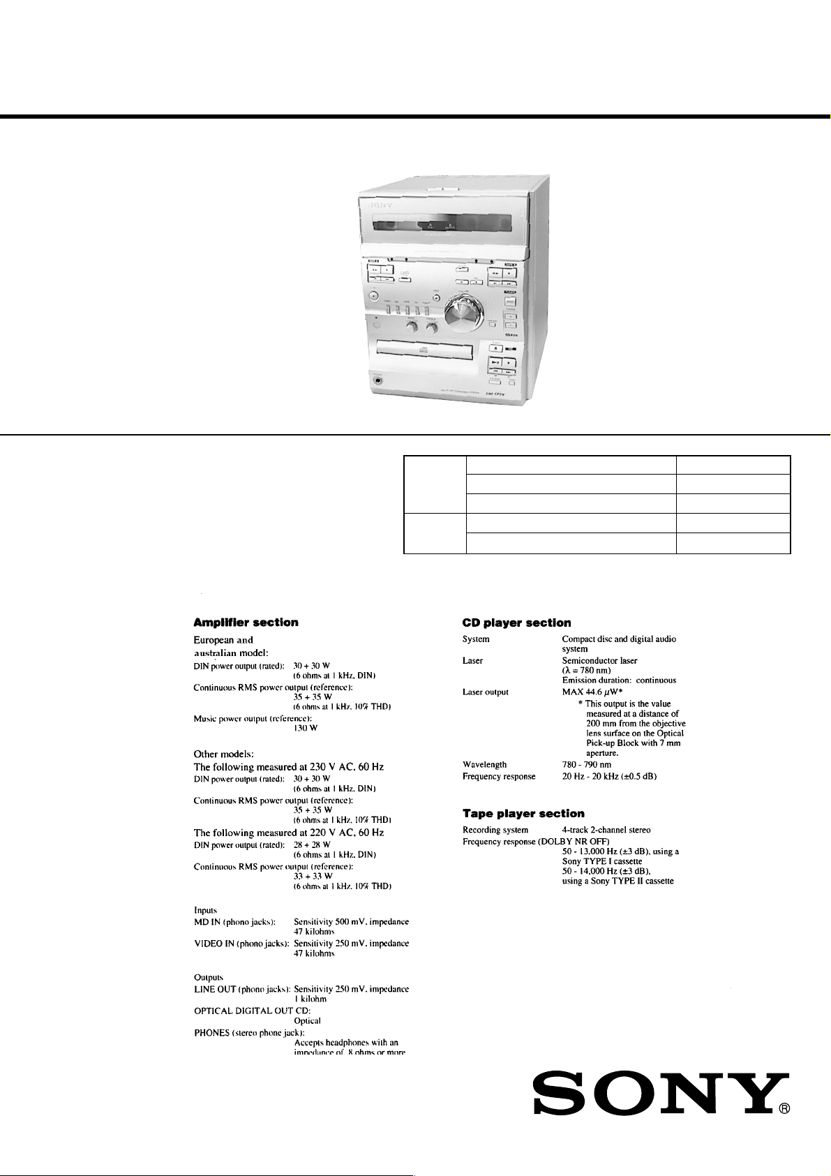
HCD-CP2
SERVICE MANUAL
HCD-CP2 is the Amplifier, CD player,
Tape Deck and Tuner section in
CMT-CP2.
Dolby noise reduction manufactured under license
from Dolby Laboratories Licensing Corporation.
“DOLBY” and the double-D symbol ; are trademarks of Dolby Laboratories Licensing Corporation.
CD
Section
Tape deck
Section
AEP Model
UK Model
E Model
Australian Model
Model Name Using Similar Mechanism NEW
CD Mechanism Type KSL-2130CCP/K1N
Optical Pick-up Name KSS-213C/K1N
Model Name Using Similar Mechanism HCD-W550
Tape Transport Mechanism Type TCM-220WR2E
SPECIFICATIONS
– Continued on next page –
MICRO HiFi COMPONENT SYSTEM
Page 2
TABLE OF CONTENTS
1. SERVICING NOTES ............................................... 3
2. GENERAL
Location of Controls ....................................................... 4
Setting the Time .............................................................. 5
3. DISASSEMBLY ......................................................... 6
4. TEST MODE.............................................................. 11
5. MECHANICAL ADJUSTMENTS ....................... 14
6. ELECTRICAL ADJUSTMENTS......................... 14
7. DIAGRAMS
7-1. Block Diagram – CD Section – ...................................... 19
7-2. Block Diagram – TAPE DECK Section – ...................... 20
7-3. Block Diagram – MAIN Section – ................................. 21
7-4. Block Diagram
– DISPLAY/POWER SUPPLY Section – ...................... 22
7-5. Note for Printed Wiring Boards and
Schematic Diagrams ....................................................... 23
7-6. Printed Wiring Board – CD Section – ............................ 24
7-7. Schematic Diagram – CD Section – ............................... 25
7-8. Printed Wiring Boards – TAPE DECK Section – .......... 26
7-9. Schematic Diagram – TAPE DECK Section – ............... 27
7-10. Printed Wiring Board – MAIN Board – ......................... 28
7-11. Printed Wiring Boards – LCD/LOADING Boards – ..... 29
7-12. Schematic Diagram – MAIN Section (1/3) –................. 31
7-13. Schematic Diagram – MAIN Section (2/3) –................. 32
7-14. Schematic Diagram – MAIN Section (3/3) –................. 33
7-15. Printed W iring Boards
– AMP/HEADPHONE Boards – .................................... 34
7-16. Schematic Diagram – POWER AMP Section – ............. 35
7-17. Printed Wiring Board – CONTROL Board – ................. 36
7-18. Schematic Diagram – KEY CONTROL Section – ........ 37
7-19. Printed Wiring Board – POWER Board – ...................... 38
7-20. Schematic Diagram – POWER SUPPLY Section –....... 38
7-21. IC Pin Function Description ........................................... 44
SAFETY-RELATED COMPONENT WARNING!!
COMPONENTS IDENTIFIED BY MARK 0 OR DOTTED
LINE WITH MARK 0 ON THE SCHEMATIC DIA GRAMS
AND IN THE PARTS LIST ARE CRITICAL TO SAFE
OPERATION. REPLACE THESE COMPONENTS WITH
SONY PARTS WHOSE PART NUMBERS APPEAR AS
SHOWN IN THIS MANU AL OR IN SUPPLEMENTS PUBLISHED BY SONY.
2
8. EXPLODED VIEWS................................................ 47
9. ELECTRICAL PARTS LIST ............................... 54
Page 3
SECTION 1
SERVICING NOTES
NOTES ON HANDLING THE OPTICAL PICK-UP
BLOCK OR BASE UNIT
The laser diode in the optical pick-up block may suffer electrostatic break-down because of the potential difference generated
by the charged electrostatic load, etc. on clothing and the human
body.
During repair, pay attention to electrostatic break-down and also
use the procedure in the printed matter which is included in the
repair parts.
The flexible board is easily damaged and should be handled with
care.
NOTES ON LASER DIODE EMISSION CHECK
The laser beam on this model is concentrated so as to be focused
on the disc reflective surface by the objective lens in the optical
pick-up block. Therefore, when checking the laser diode emission, observe from more than 30 cm away from the objecti ve lens.
Notes on chip component replacement
• Never reuse a disconnected chip component.
• Notice that the minus side of a tantalum capacitor may be damaged by heat.
Flexible Circuit Board Repairing
• Keep the temperature of the soldering iron around 270 ˚C during repairing.
• Do not touch the soldering iron on the same conductor of the
circuit board (within 3 times).
• Be careful not to apply force on the conductor when soldering
or unsoldering.
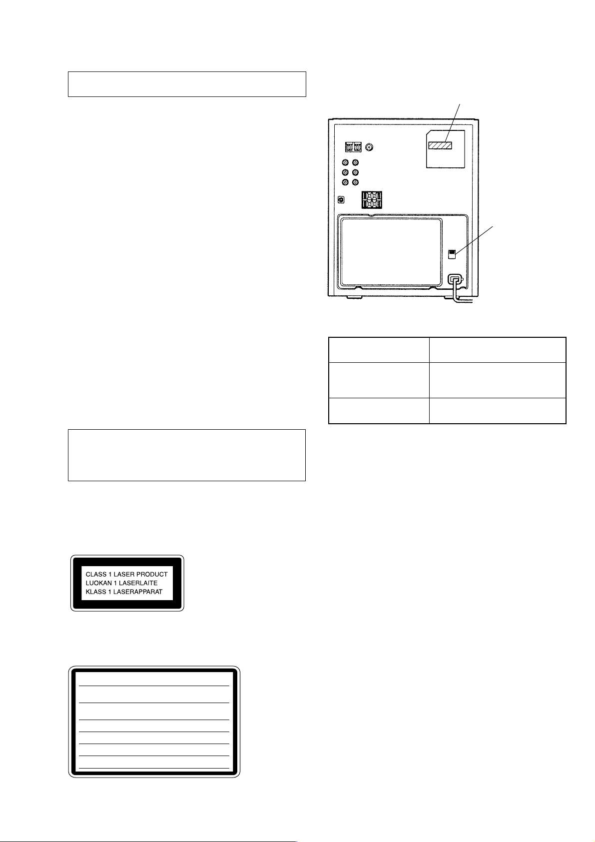
• MODEL IDENTIFICATION
– Rear Panel –
Power Voltage Indication
VOLTAGE SELECTOR
Switch
Model Pow er V oltage Indication
AEP, UK and
North European and AC: 230 V -50 Hz 70 W
Australian models
Saudi Arabia, AC: 110 – 120/
Singapore models 220 – 240 V -50/60 Hz 70 W
CAUTION
Use of controls or adjustments or performance of procedures
other than those specified herein may result in hazardous radiation exposure.
This appliance is classified as a CLASS 1 LASER product.
The CLASS 1 LASER PRODUCT MARKING is located on
the rear exterior.
Laser component in this product is capable of emitting radiation
exceeding the limit for Class 1.
The following caution label is located inside the unit.
CAUTION :
INTERLOCKS DEFEATED. AVOID EXPOSURE TO BEAM.
ADVARSEL :
SIKKERHEDSAFBRYDERE ER UDE AF FUNKTION. UNDGÅ UDSAETTELSE
FOR STRÅLING.
VORSICHT :
ABDECKUNG GEÖFFNET UND SICHEREITSVERRIEGELUNG
ÜBERBRÜCKT. NICHT DEM STRAHL AUSSETZEN.
VARO! :
TIINA NÄKYMÄTTÖMÄLLE LASERSÄTEILYLLE. ÄLÄ KATSO SÄTEESEEN.
VARNING :
OCH SPÄRREN ÄR URKOPPLAD. BETRAKTA EJ STRÅLEN.
ADVERSEL :
SIKKERHEDSLÅS BRYTES. UNNGÅ EKSPONERING FOR STRÅLEN.
VIGYAZAT! :
GÁRVESZÉLY! KERÜLJE A BESUGÁRZÁST!
INVISIBLE LASER RADIATION WHEN OPEN AND
USYNLIG LASERSTRÅLING VED ÅBNING NÅR
UNSICHTBARE LASERSTRAHLUNG, WENN
AVATTAESSA JA SUOJALUKITUS OHITETTAESSA OLET ALT-
OSYNLING LASERSTRÅLING NÄR DENNA DEL ÄR ÖPPNAD
USYNLIG LASERSTRÅLING NÅR DEKSEL ÅPNES OG
A BURKOLAT NYITÁSAKOR LÁTHATATLAN LÉZERSU-
3
Page 4
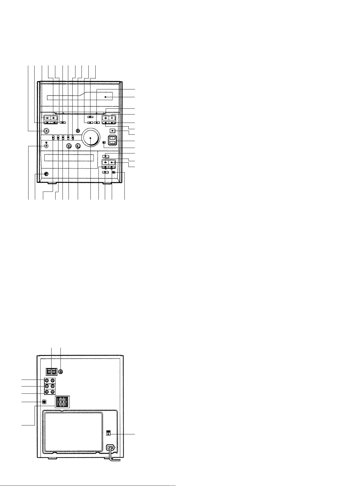
• LOCATION OF CONTROLS
– Front View –
3
wg
wf
– Rear View –
4
5
6
7
45217
6
wk
21
8
9
e;wlwh
0
ea
qa
SECTION 2
GENERAL
1 STANDBY ?/1 button and indicator
2 TAPE A m button
3 TAPE A Y button
qs
qd
qf
qg
qh
qj
qk
ql
w;
wa
ws
wd
eswj
eg
efed
4 TAPE A x button
5 TAPE A M button
6 HI-SPEED DUBBING button and indicator
7 CD button and indicator
8 TUNER button and indicator
9 DSG button and indicator
0 X button
qa CD SYNC button and indicator
qs REC z button
qd Liquid crystal display
qf TAPE B Y button
qg TAPE B x button
qh TAPE B M button
qj TAPE B m button
qk TUNER BAND button
ql TUNING +/– buttons
w; TUNING MODE button
wa EJECT Z button
ws CD u button
wd CD x button
wf Remote sensor
wg PHONES jack
wh VIDEO button and indicator
wj MD button and indicator
wk TAPE button and indicator
wl BASS switch
e; TREBLE switch
ea VOLUME knob
es CD . m button
ed PLAY MODE button
ef CD > M button
eg REPEAT button
1 AM ANTENNA terminals
2 FM ANTENNA jack or terminals
3 VOLTAGE SELECTOR switch
(Saudi Arabia, singapore models)
4 LINE OUT jacks
5 MD IN jacks
6 VIDEO IN jacks
7 DIGITAL OUT OPTICAL (CD) connector
8 SPEAKER terminals
8
4
3
Page 5
This section is extracted from
instruction manual.
5
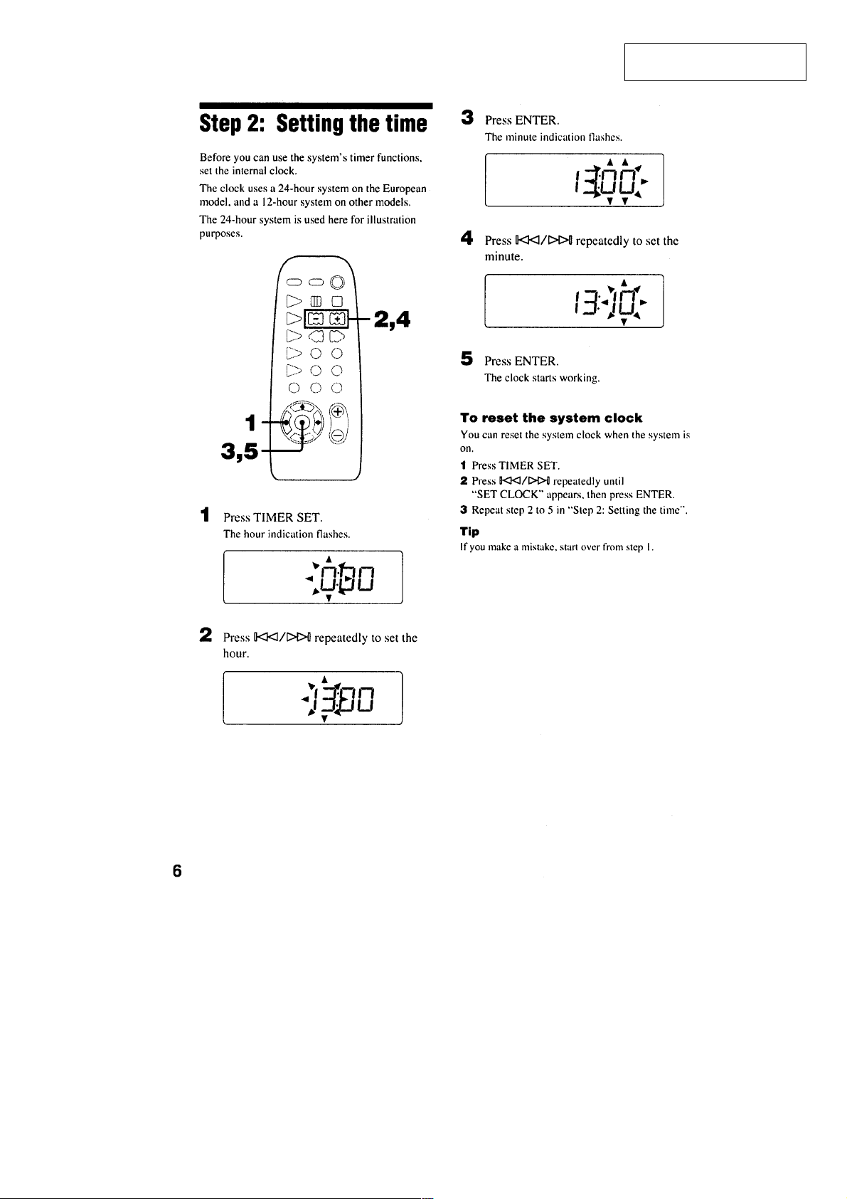
Page 6
SECTION 3
DISASSEMBLY
Note: Follow the disassembly procedure in the numerical order given.
COVER (UPPER)
3 cover (upper)
1 two case screws
FRONT PANEL ASSY
2 connector
(CN808)
2 six screws
(BTP3 × 8)
1 two case screws
2 connector
(CN805)
1 two flat cables
6 front panel assy
4 screw
(KTP3 × 6)
5 two bosses
3 two screws
(BTP3 × 8)
2 connector
(CN311)
(CN601, 1001)
(To page 8)
1 three flat cables
(CN801, 803, 806)
4 screws
(KTP3 × 6)
6
Page 7
TAPE MECHANISM DECK (TCM-220WR2E)
)
4 Push these buttons.
1 five screws
(BTP3 × 8)
2 screws (DIA. 12
3 harness
AUDIO BOARD
4 four screws
5 AUDIO board
5 TCM-220WR2E
1 connector
(CN651)
2 two rivets
(BTP2.6 × 4)
3 Break the soldering of
two flexible flat cables.
7
Page 8
CAPSTAN MOTOR
)
r
1 Break the soldering of
motor lead.
3 capstan motor
2 two screws
(BTP2.6 × 8
CD MECHANISM DECK (KSL-2130CCP/K1N)
3 two screws
(BTP3 × 8)
3 two screws
(BTP3 × 8)
4 CD mechanism deck
(KSL-2130CCP/K1N)
1 flat cable
(CN301)
2 connecto
(CN900)
8
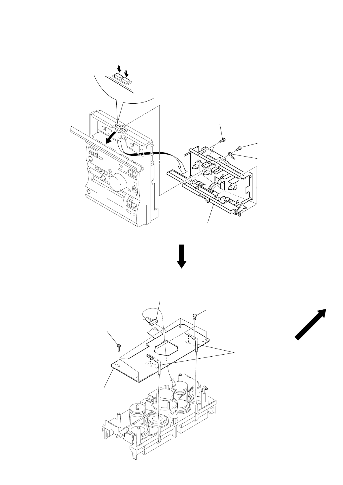
Page 9
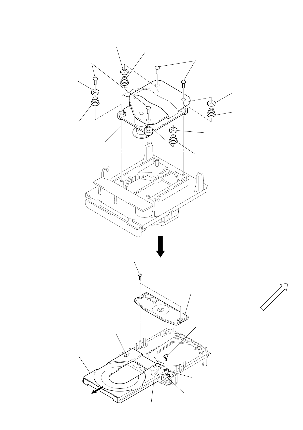
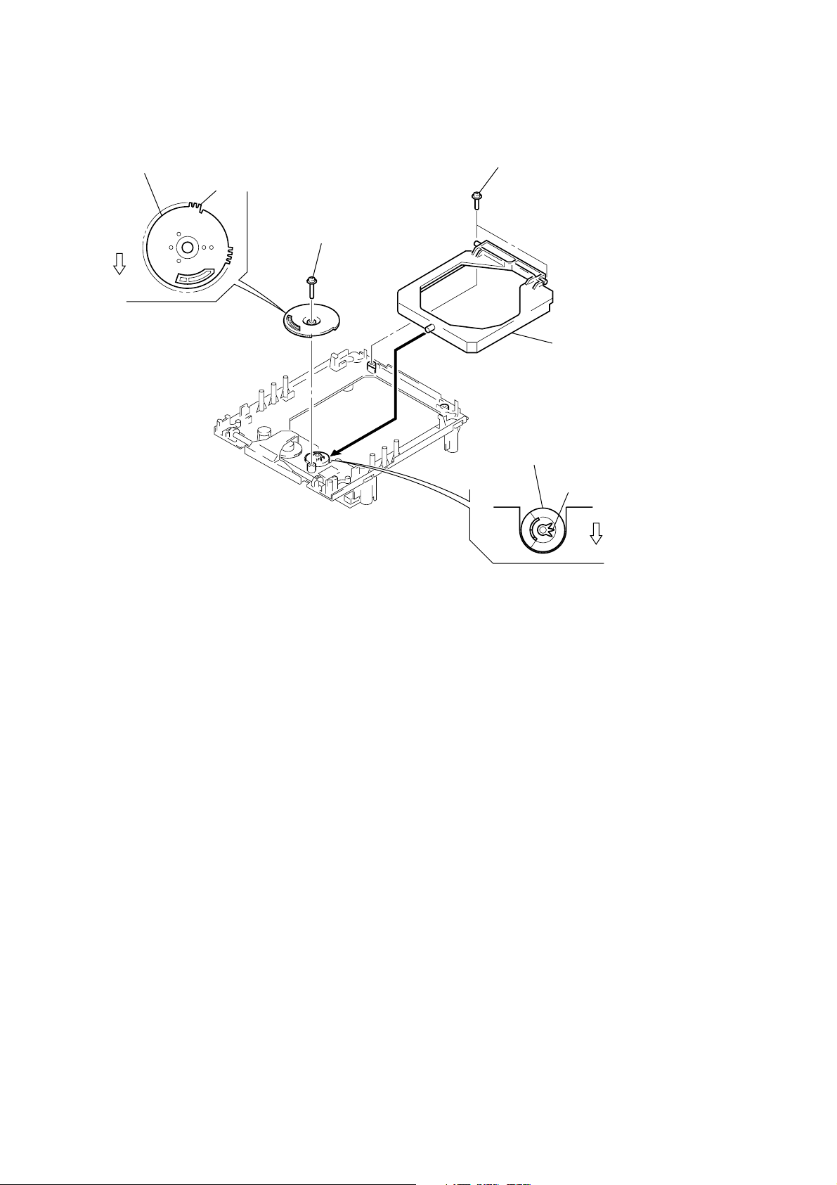
CD BOLCK ASSY
)
1 two screws
2 washer (2130)
3 coil spring
(front)
2 washer (2130)
(P2.6 × 10)
4 CD block assy
3 coil spring (front)
1 two screws
(P2.6 × 10)
2 washer (2130)
3 coil spring (front
2 washer (2130)
3 coil spring (front)
TRAY (2130)
4 Pull the tray (2130).
8 Remove the tray (2130).
1 two screws
(PTPWH2.6 × 7)
2 chucking yoke (K)
6 damper (S)
7 lock lever
A
5 claw
7 lock lever
3 Rotate the control cam
in the direction of arrow A.
9
Page 10
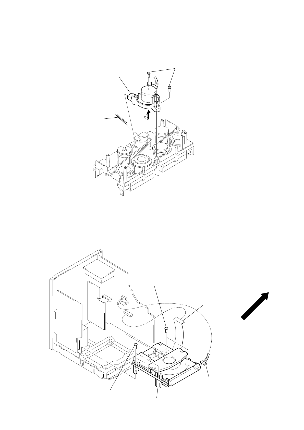
• SUB CHASSIS (2130) INSTALLATION
Note: Follow the assembly procedure in the numerical order given.
2 Install the drive gear with gear
position as shown in figure.
gear
front side
5 two screws
(PTPWH2.6 × 7)
3 screw
(PTPWH2.6 × 16)
4 sub chassis (2130)
1 Install the control cam
with gear position as shown
in figure.
gear
front side
10
Page 11
SECTION 4
TEST MODE
[MC Cold Reset]
• The cold reset clears all data including preset data stored in the
RAM to initial conditions. Execute this mode when returning
the set to the customer.
Procedure:
1. While pressing the ?/1 button, connect the power cord.
2. The set is reset.
[CD Aging Mode]
This mode can be used for operation check of CD section.
Procedure:
1. Load a CD disc.
2. Set to standby state.
3. Press three b uttons of x (TAPE B), x (CD), and [TUNER]
simultaneously.
4. The aging is executed in bellow sequence.
5. To release from the aging mode, press the ?/1 button to turn
the power OFF.
Aging mode sequence:
Start
Open the disc tray
Aging mode sequence:
FWD Play
REC pause for 3 seconds
FWD REC
Fast forward
REV Play
REC pause for 3 seconds
Start
Shut off
1 minute
Shut off
3 minutes
Shut off
1 minute
Close the disc tray
Play the last track
[Tape Deck Aging Mode]
This mode can be used for operation check of tape deck section.
Procedure:
1. Set a tape in the tape deck-B.
2. Set to standby state.
3. Press three buttons of x (TAPE B), x (CD), and [TAPE]
simultaneously.
4. The aging is executed in bellow sequence.
5. To release from the aging mode, press the ?/1 button to turn
the power OFF.
REV REC
3 minutes
Rewind
Shut off
[Liquid Crystal Display All Lit Check Mode]
Procedure:
1. Set to standby state.
2. Press three buttons of
x (TAPE B), x (CD), and [VIDEO]
simultaneously.
3. Liquid crystal display are all turned on.
4. To release from this mode, press the ?/1 button to turn the
power OFF.
[ROM Version Display Mode]
Procedure:
1. Set to standby state.
2. Press three buttons of x (TAPE B), x (CD), and [DSG] simultaneously.
3. The ROM version is displayed.
11
Page 12
[CD TEST MODE]
)
In the CD test mode, the set works as following sequence.
CD test mode sequence:
1. Enter the CD test mode
2. STOP mode
Press the u (CD)
button.
3. FOCUS mode
Press the u (CD)
button.
4. ALL SERVO
ON mode
Press the u (CD)
button.
5. LPC OFF
Press the u (CD)
button.
6. TRACKING
GAIN UP mode
Press the u (CD)
button.
mode
Press the x (CD)
button.
Press the x (CD)
button.
Press the x (CD)
button.
Press the x (CD)
button.
2. STOP Mode
1. Press the [EJECT ] button twice to disc tray open and close.
Z
(All servo ON)
2. Press the
> and . button to move the optical pick-up
to position of the track where signal is recorded.
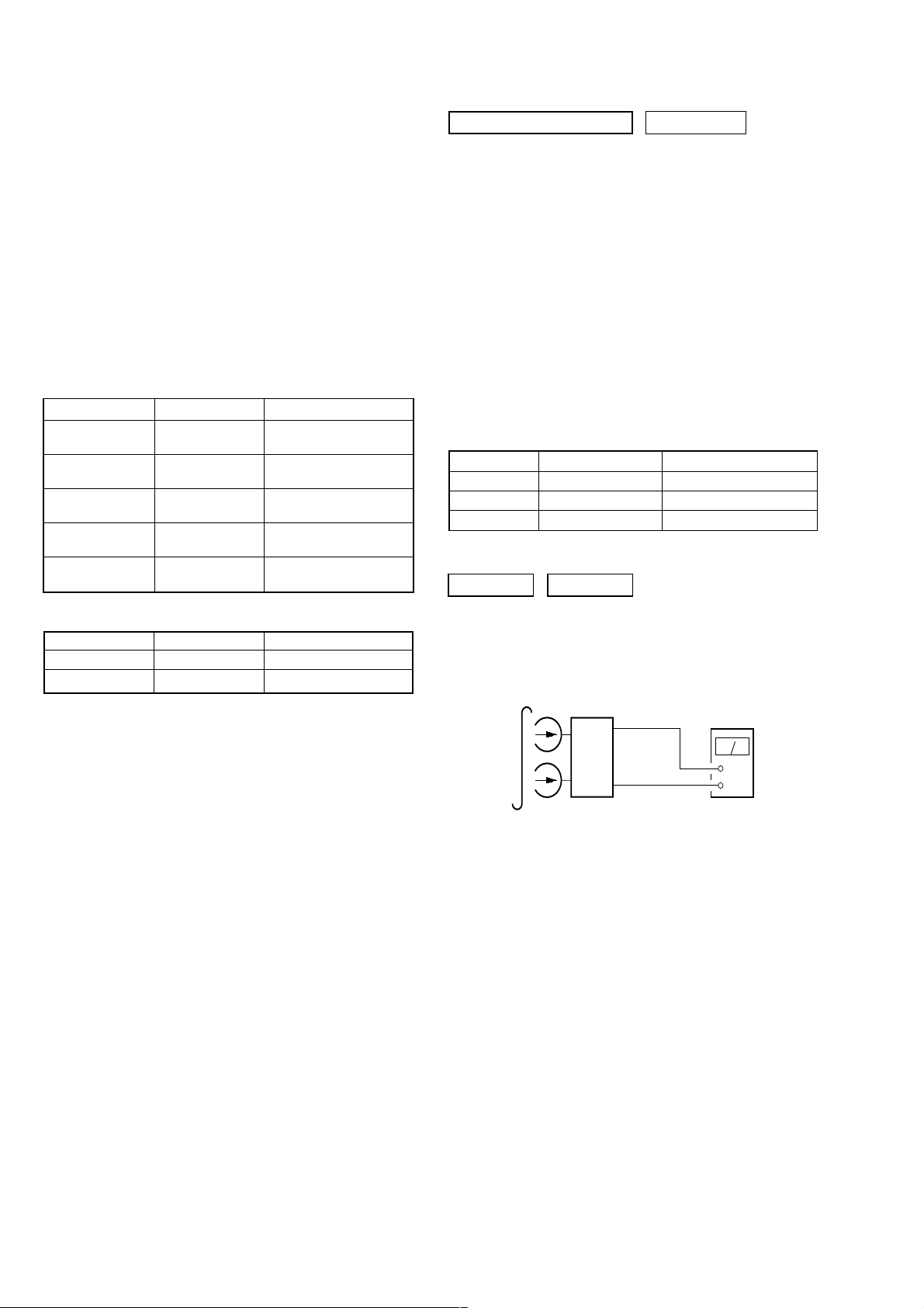
3. FOCUS Mode
1. Press the u button to enter the FOCUS mode and display
as below . (Focus servo ON. CLV-S , tacking and sled servo OFF)
Display
F
* * * *
2. Connect an oscilloscope to TP (TE) and TP (VC) on the CD
board.
Connection:
oscilloscope
(DC range)
BD board
TP (TE)
TP (VC)
+
–
3. Conf irm the traverse level and center values of waveform satisfy specified value as follows.
Traverse waveform
Center of the waveform
Note: TRACKING GAIN UP mode is not used in servicing.
1. Entering the CD Test Mode
1. Press the ?/1 button to turn the power ON.
2. Press the [EJECT ] button to open the disc tray, and put a
Z
disc.
3. Press the
4. Press the
[EJECT ] button to close the disc tray.
?/1 button to turn the power OFF.
Z
5. While pressing the both x (TAPE B) and x (CD) buttons,
press the [CD] (function) button.
6. Enter the CD test mode, and display as below for a few seconds.
Display
AUTO
F
Note: Lights up “STEREO” indication :LPC ON
Does not light up “STEREO” indication :LPC OFF
*) LPC: Laser power control
* * * *
STEREO
7. Then display as below, and enter the STOP mode.
Display
STEREO
* * * *
0 V
Specified value:
traverse level A : more than 350 mVp-p
center values B : 0 ± 50 mV
A
B (DC
voltage
12
Page 13

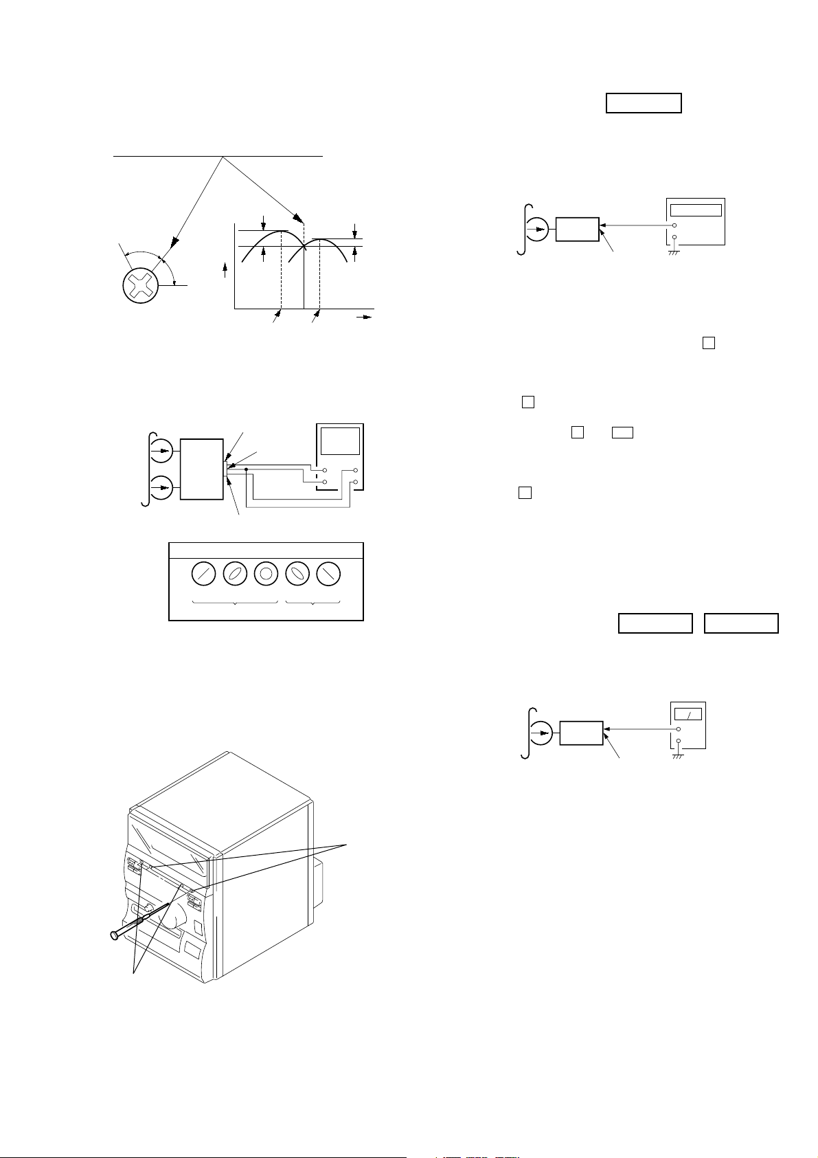
4. ALL SERVO ON Mode
V
1. Press the u button to enter the ALL SER VO ON mode and
display as below. (All servo ON)
Display
STEREO
P L
2. Connect an oscilloscope to TP (RF) and TP (VC) on the CD
board.
Connection:
BD board
* * * *
oscilloscope
(DC range)
Connecting Location:
– CD BOARD (Conductor Side) –
TP (GND)
TP (TE)
TP (VC)
IC701
IC703
TP (RF)
TP (RF)
TP (VC)
3. Confirm the RF level of waveform satisfy specified value as
follows.
RF signal waveform
Specified value:
RF level: 1 ± 0.3 Vp-p
5. LPC OFF Mode
1. Press the
as below. (LPC OFF)
x button to enter the LPC OFF mode and display
P L
* * * *
+
–
VOLT/DIV: 200 m
TIME/DIV: 500 ns
level:
1.2 ± 0.1 Vp-p
Display
2. Conf irm the RF le v el of w aveform is the same as the RF level
in “4. ALL SERVO ON mode”.
If the RF level is down from the RF level in “4. ALL SERVO
ON mode”, measure again after clean the object lens by an
applicator with lens cleaning liquid.
6. Releasing the CD Test Mode
1. Press the x (CD) button to stop rotate the disc.
2. Press the ?/1 button to release the CD test mode and turn the
power OFF.
13
Page 14
SECTION 5
MECHANICAL ADJUSTMENTS
SECTION 6
ELECTRICAL ADJUSTMENTS
PRECAUTION
1. Clean the follo wing parts with a denatured-alcohol-moistened
swab:
record/playback heads pinch rollers
erase head rubber belts
capstan idlers
2. Demagnetize the record/playback head with a head demagnetizer.
3. Do not use a magnetized screwdriver for the adjustments.
4. After the adjustments, apply suitable locking compound to
the parts adjusted.
5. The adjustments should be performed with the rated power
supply voltage unless otherwise noted.
• Torque Measurement
• Tape Tension Measurement
• T orque Measurement
Mode Torque Meter Meter Reading
Forward CQ-102C
Forward
Back Tension (0.026 – 0.082 oz•inch)
Reverse CQ-102RC
Reverse
Back Tension (0.026 – 0.082 oz•inch)
FF, REW CQ-201B
CQ-102C
CQ-102RC
36 to 61 g•cm
(0.50 – 0.84 oz•inch)
2 to 6 g•cm
36 to 61 g•cm
(0.50 – 0.84 oz•inch)
2 to 6 g•cm
61 to 143 g•cm
(0.85 – 1.98 oz•inch)
0 dB=0.775 VTAPE DECK SECTION
1. Demagnetize the record/playback head with a head demagnetizer. (Do not bring the head demagnetizer close to the erase
head)
2. Do not use a magnetized screwdriver for the adjustments.
3. After the adjustments, apply suitable locking compound to
the parts adjust.
4. The adjustments should be performed with the rated power
supply voltage unless otherwise noted.
5. The adjustments should be performed in the order given in
this service manual. (As a general rule, playback circuit adjustment should be completed before performing recording
circuit adjustment)
6. The adjustments should be performed for both L-CH and Rch.
7. Switches and controls should be set as follows unless otherwise specified.
• Test T ape
Tape Signal Used for
P-4-A100 10 kHz, –10 dB Azimuth Adjustment
WS-48B 3 kHz, 0 dB Tape Speed Adjustment
P-4-L300 315 Hz, 0 dB Level Adjustment
Record/ Playback Head Azimuth Adjustment
DECK A DECK B
• Tape T ension Measurement
Mode Tension Meter Meter Reading
Forward CQ-403A more than 100 g (3.52 oz)
Reverse CQ-403R more than 100 g (3.52 oz)
Note: Perform this adjustments for both decks
Procedure:
test tape
P-4-A100
(10 kHz, –10 dB)
MAIN board
IC401
Pin 8 (L-CH)
Pin eg (R-CH)
set
MAIN board
IC401
Pin rs
level meter
+
–
14
Page 15
+
–
set
test tape
WS-48B
(3 kHz, 0 dB)
MAIN board
IC401(Pin 8 : L-CH)
(Pin eg : R-CH)
frequency counter
(
)
1. Mode: Playback (FWD)
e
2. T urn the adjustment screw and check output peaks. If the peaks
do not match for L-CH and R-CH, turn the adjustment screw
so that outputs match within 1dB of peak.
within
output
level
1dB
L-CH
peak
R-CH
peak
within
1dB
Screw
position
L-CH
peak
Screw
position
R-CH
peak
3. Mode: Playback (FWD)
test tape
P-4-A100
(10 kHz, –10 dB)
L-CH
MAIN
board
IC401
set
R-CH
waveform of oscilloscope
pin 8
L
R
pin
pin rs
eg
oscilloscope
H
V
Tape Speed Adjustment DECK A
Procedure:
Turn the power switch on.
Mode: Playback (FWD)
1. Insert the WS-48B into the deck A and the blank tape into the
deck B.
2. Press the [HI-SPEED DUBBING] button and X button.
Then at HIGH speed dubbing.
3. Adjust RV652 on the A UDIO board do that frequency counter
reads 6,000 ± 180 Hz.
4. Press the x (TAPE A or B) button to stop the HIGH speed
dubbing.
5. Press the [REC ], X and Y button.
z
Then at NORMAL speed dubbing.
6. Adjust RV651 on the A UDIO board so that frequency counter
reads 3,000 ± 90 Hz.
7. Press the
x (TAPE A or B) b utton to stop the NORMAL speed
dubbing.
8. Frequency diff erence between deck A and deck B the beginning of the tape should be within ± 1.5%.
Adjustment Location: AUDIO and MAIN boards
in phase 45 °
90 ° 135 ° 180 °
good
wrong
4. Repeat steps 1 to 3 in playback (REV) mode.
5. After the adjustments, apply suitable locking compound to the
pats adjusted.
Adjustment Location: Record/Playback Head (Deck A and B)
and MAIN board.
revers
Sample Value of Wow and flutter: 0.3% or less W. RMS (JIS)
(WS-48B)
Playback level Adjustment
DECK A DECK B
Procedure:
Mode: Playback (FWD)
test tape
P-4-L300
(315 Hz, 0 dB)
set
MAIN board
IC401 (Pin 8 : L-CH)
level meter
+
–
Pin eg : R-CH
Deck A is RV311 (L-CH) and RV411 (R-CH), Deck B is RV301
(L-CH) and RV401 (R-CH) so that adjustment within adjustment
level as follows.
Adjustment Level:
IC401 PB level: 301.5 to 338.3 mV (–8.2 to –7.2 dB) level
difference between the channels: within ± 0.5 dB
Adjustment Location: AUDIO and MAIN boards
forward
15
Page 16
Record bias Current Adjustment
(
)
r
(
)
r
Procedure:
1. Mode: Record
Pin 6 (L-CH) of IC401 on the MAIN board.
Pin ej (R-CH) of IC401 on the MAIN board.
1) 315 Hz
2) 10 kHz
AF OSC
attenuator
50 mV (–23.8 dB)
600 Ω
DECK B
set
Adjustment Location:
– MAIN BOARD (Component Side) –
blank tape
CN-123
Pin rs (GND) of IC401 on the MAIN
board.
2. Mode: Playback
recorded
portion
set
IC401 (Pin 8 : L-CH)
level mete
+
–
Pin eg : R-CH
Confirm playback the signal recorded in step 1 become adjustable
limits as follows.
If these levels do not adjustable limits, adjustment the RV341 (LCH) and RV441 (R-CH) on the AUDIO board to repeat steps 1
and 2.
Adjustable limits: Playback output of 315 Hz to playback output
of 10 kHz: 0 ± 0.5 dB
Adjustment Location: AUDIO and MAIN boards
Record Level Adjustment
DECK B
Procedure:
1. Mode: Record
Pin 6 (L-CH) of IC401 on the MAIN board.
Pin
ej (R-CH) of IC401 on the MAIN board.
AF OSC
315 Hz, 50 mV (–23.8 dB)
600 Ω
attenuator
blank tape
CS-123
set
RV351
RECORD
LEVEL
IC401
RV301
– AUDIO BOARD (Conductor Side) –
TAPE SPEED
(NORMAL) (HIGH)
RV651
PB
LEVEL
RV311 L
RV411 R
– DECK A –– DECK B –
RV652
RV301
L
R
RV401
RECORD
BIAS CURRENT
RL
RV341
RV441
PB LEVEL
* As the adjustment parts is mounted on the component side, ad-
just it through a hole in the AUDIO board form conductor side.
(Except RV431, 441)
Pin
rs (GND) of IC401 on the MAIN board.
2. Mode: Playback
recorded
portion
set
IC401 (Pin 8 : L-CH)
level mete
+
–
Pin eg : R-CH
Confirm playback the signal recorded in step 1 become adjustable
limits as follows.
If these levels do not adjustable limits, adjustment the RV301 (LCH) and R V351 (R-CH) on the MAIN board to repeat steps 1 and
2.
Adjustable limits:
IC401 PB level: 36.7 to 41.1 mV (–26.5 to –25.5 dB)
Adjustment Location: MAIN board
16
Page 17
CD SECTION
V
Note:
1. CD Block is basically constructed to operate without
adjustment. Therefore, check each item in order given.
2. Use YEDS-18 disc (3-702-101-01) unless otherwise indicated.
3. Use an oscilloscope with more than 10 MΩ impedance.
4. Clean the object lens by an applicator with neutral detergent
when the signal level is low than specified value with the
following checks.
5. Adjust the focus bias adjustment when optical block is replaced.
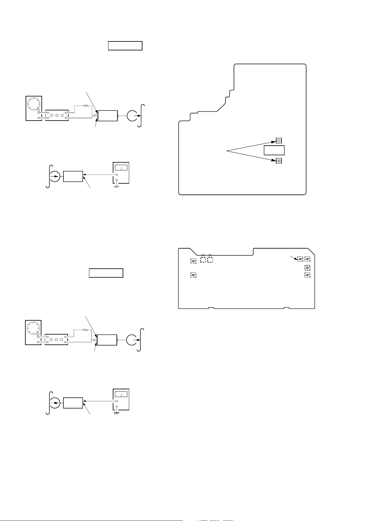
Focus Bias Check
oscilloscope
(DC range)
BD board
TP (RF)
TP (VC)
+
–
Procedure :
1. Connect oscilloscope to TP (RF) and TP (GND) on CD board.
2. Turned Power switch on.
3. Put disc (YEDS-18) in and press the [CD ] button to play-
u
back.
4. Confirm that oscilloscope waveform is as shown in the figure
below. (eye pattern)
A good eye pattern means that the diamond shape ( ) in the
s
center of the waveform can be clearly distinguished.
VOLT/DIV: 200 m
TIME/DIV: 500 ns
level:
1.2 ± 0.1 Vp-p
Adjustment Location:
– CD BOARD (Conductor Side) –
TP (GND)
IC701
IC703
TP (RF)
17
Page 18

18
Page 19
7-1. BLOCK DIAGRAM – CD Section –
HCD-CP2
SECTION 7
DIAGRAMS
DETECTOR
A
D
C
B
F
E
OPTICAL PICK-UP
(KSS-213C/K1N)
LASER DIODE
I-V AMP
DIGITAL
CLV
MDP
21
FILTER
3129
3330
FILI
PCO
FILO
CLTV
DIGITAL PLL
DEMODULATOR
PROCESSOR
SQSO
SQCK
SENS
5 4 6 7 9 85758 59
ERROR
CORRECTOR
EFM
SUB-CODE
CPU INTERFACE
DATA
CLOK
XLAT
SCOR
SBSO
INTERNAL BUS
XLON (MUTE)
EXCK
17 15
B+
16K
RAM
SPOA (LIMIT)
PCMD
BCK
LRCK
GTOP/
C2PO/
C2PO
D/A INTERFACE
RFCK/MNT1/XUGF
WFCK
EMPH
XROF/MNT3/GFS
DOUT
DIGITAL
OUT
S701
(LIMIT)
41
43
39
50
47
56
54 55
49
53
PCMDI
42
BCKI
LRCKI
EMPHI
SERIAL
INPUT
INTERFACE
CLOCK
GENERATOR
OSC
XTAI
SYSM (MUTE)
62 70
X701
16.9344MHz
44
40
XTAO
71
SAMPLING
DIGITAL
FILTER
PWM
AOUT1
AOUT2
C4M
XTSL
OVER
NOISE
SHAPER
PWM
65
76
52
51
75 66
AIN2
LOUT2
74 67
R-CH
AIN1
LOUT1
DIGITAL SIGNAL PROCESSOR,
CLV SERVO, D/A CONVERTER
IC703
PD1 I-V AMP
A
D
C
B
F
E
38
39
PD1
PD2 I-V AMP
PD2
+
F
41
E
42
RF
SUMMING
AMP
RF AMP,
FOCUS/TRACKING
SERVO
IC701 (1/2)
I-V
AMP
FOCUS
ERROR
AMP
TRACKING
ERROR
AMP
RF O
RF I
FOCUS OK
COMPARATOR
MIRR
AMP
DEFECT
AMP
FEO
FE BIAS
TEO
RF
33
32
FOCUS OK
AMP
TTL
IIL
1
40
45
FEI FE O
2
TEI
47
TTL
IIL
IIL
IIL DATA REGISTER
TTL
FOCUS PHASE
COMPENSATION
TRACKING PHASE
COMPENSATION
FOK
DATA
CLK
XLT
LOCK
XRST
SENS1
C.OUT
SENS2
TA O
27
22
20
21
19
23
25
24
26
6
13
35
ASYI
37
ASYO
38
XPCK/MNTO/XPCK
48
FOK
18
DATO
12
CLKO
14
XLTO
13
79
XRST
SEIN
10
CNIN
11
ASYMMETRY
CORRECTION
SERVO AUTO SEQUENCER
LD
LD
PD
PD
2-AXIS
DEVICE
(FOCUS)
05
T+
T–
(TRACKING)
F+
F–
(SPINDLE)
POWER CONTROL
M702
(SLED)
M701
AUTOMATIC
Q701
M
M
LD
36
LD
AMPPDAMP
FOCUS/TRACKING COIL DRIVE,
SPINDLE/SLED MOTOR DRIVE
IC702
T+
17
18
26
27
2
1
12
11
T–
F+
F–
SL+
SL–
SP+
SP–
TRACKING
COIL DRIVE
FOCUS
COIL DRIVE
SLED
MOTOR DRIVE
SPINDLE
MOTOR DRIVE
PD
37
(TIN)
20
FIN
25
SLED SERVO
IC701 (2/2)
SLIN
SPIN
SL O
3
16 14
9 1514
SLED
AMP
SL P
SPO
MUTE
7
SPIN
4
C-XRST
55
SENS2
76
77
54
51
52
C-DATA
C-SQCK
C-SQSO
CD-SENS1
SYSTEM CONTROLLER
IC802 (1/4)
67
C-CLK
C-XLAT
C-MUTE
62
C-SCOR
69
OPTICAL
TRANSCEIVER
IC308
• SIGNAL PATH
CD L-CH
A
(Page 21)
OPTICAL
DIGITAL
OUT (CD)
: CD PLAY (ANALOG OUT)
: CD PLAY (DIGITAL OUT)
R-CH : Same as L-CH.
1919
Page 20
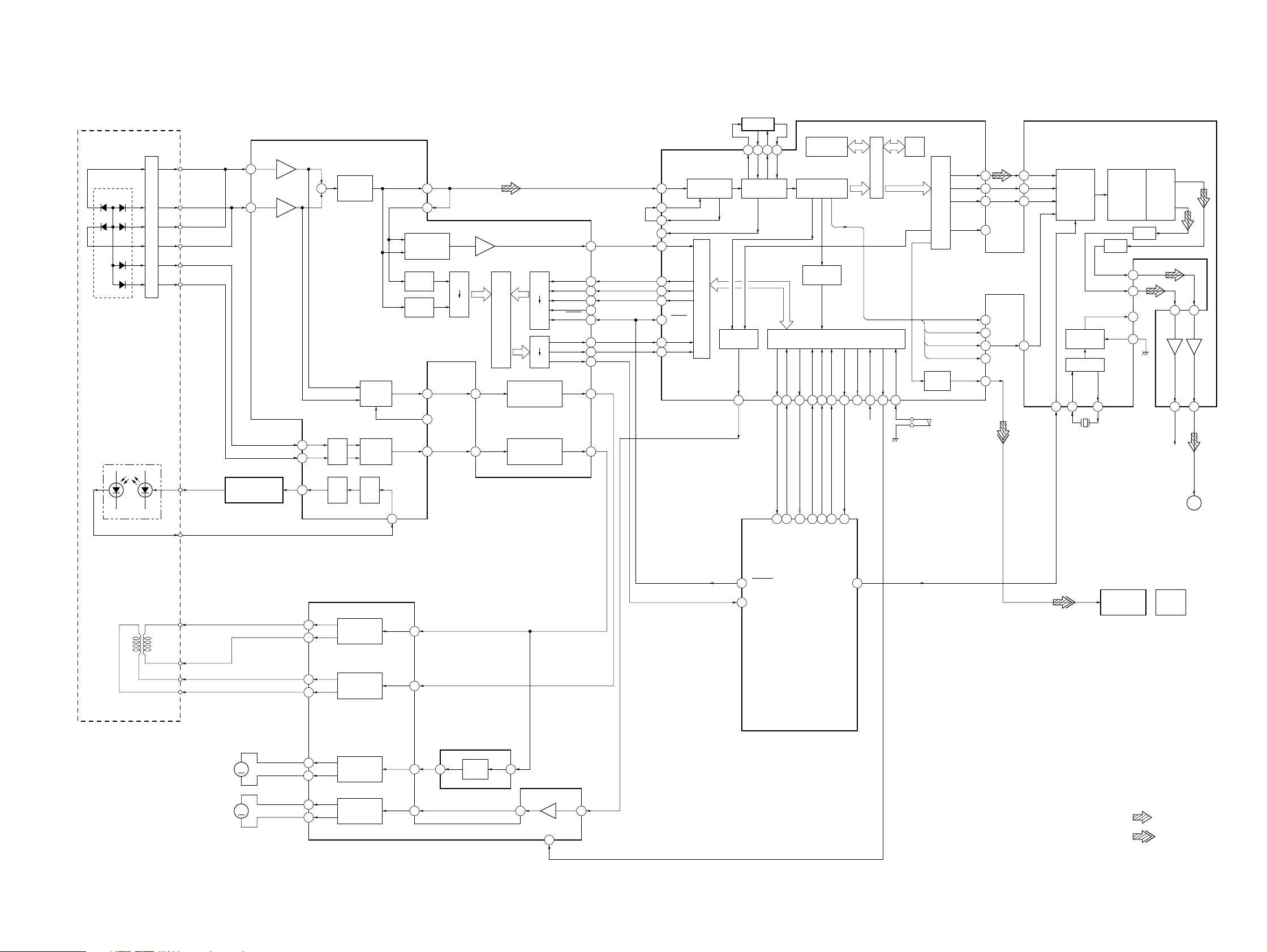
HCD-CP2
7-2. BLOCK DIAGRAM – TAPE DECK Section –
HP101
(PLAYBACK)
L-CH
R-CH R-CH
HRPE101 (1/2)
(RECORD/PLAYBACK)
L-CH
R-CH R-CH
3
R-CH
2
PB EQ AMP
(DECK A)
IC611
PB EQ AMP
(DECK B)
IC601
REC/PB SWITCHING
IC602
1
R-CH
RV311
PB LEVEL (L)
(DECK A)
RV301
PB LEVEL (L)
(DECK B)
4
DECK PROCESS
DECK A/B SELECT, PB/REC EQ AMP,
DOLBY NR AMP
AIN (L)
2
BIN (L)
4
NORM
25
CROM
24
METAL
23
A 120/70
15
S1004
(DECK A 120/70)
S1008
(DECK B 120/70)
IC401
70
120
BIAS
CONTROL
CIRCUIT
LM-ON/OFF
PB-A/B
122016
BIAS-ON/OFF
RM-ON/OFF
17 18191413
NORM/CROM/METAL
R-CH
NR-ON/OFF
REC/PB/PASS
NORM/HIGH
+
L.P.F.
BUFFER
28
27
AMS
CIRCUIT
21
MAOUT
MSIN
MSOUT
LED DEIVE
Q816
RIN (L)
6
DOLBY PASS
DOLBY NR
AMP
CIRCUIT
D822
HI-SPEED
DUBBING
RECOUT (L)
9
RV301
REC LEVEL (L)
(DECK B)
EQIN (L)
10
REC
EQ AMP
PBOUT (L)
EQOUT
• SIGNAL PATH
: PLAYBACK (DECK A)
8
PB-L
B
(Page 21)
: PLAYBACK (DECK B)
: RECORD
R-CH : Same as L-CH
(L)
11
REC-L
C
(Page 21)
REC/PB
D
(Page 22)
RV441
REC BIAS (R)
(DECK B)
HRPE101 (2/2)
(ERASE)
R-CH
RV341
REC BIAS (L)
(DECK B)
BIAS OSC
T621
BIAS OSC
Q621, 622
REC BIAS
SWITCH
Q623
05
C331, L331
BIAS
TRAP
B+
(A+8V)
D+5V
68
REC/PB
T-PLAY (A)
15 18
S1001
(DECK A PLAY)
1757
A/B
LINE MUTE
T-PLAY (B)
S1002
(DECK B PLAY)
79 78880
DOLBY
REC-BIAS
REC-MUTE
(DECK A HALF)
REC/PB
S1003
3
NORMAL/HI
HI DUB REC
14
T-HALF (A)
(DECK B HALF)
(DECK B REC)
ROTATION
DETECT SENSOR
(DECK A)
Q1001
16
S1006
S1009
TC-SHUT (A)
T-MODE
39
D+5V
ROTATION
DETECT SENSOR
(DECK B)
Q1002
17
TC-SHUT (B)
S1005
(DECK A REC)
SYSTEM CONTROLLER
IC802 (2/4)
10
CAP MOTOR H/L
Q406
TRIG MOTOR CON (B)
TRIG MOTOR H/L
12
13
RV652
TAPE SPEED
(HIGH)
CAPSTAN MOTOR
CONTROL SWITCH
9
CAP MOTOR CON
TRIG MOTOR CON (A)
11
5
6
RV651
TAPE SPEED
(NORMAL)
Q651
CAPSTAN
MOTOR CONTROL
Q403, 407
+12V (M)
TRIGGER MOTOR DRIVE
IC402
MOTOR
DRIVE
4
OUT1
OUT2
IN1
IN2
VZ
M1
M
(CAPSTAN)
2
10
M
M2
(TRIGGER)
20
20
TRIGGER
MOTOR CONTROL
Q408, 409
Page 21

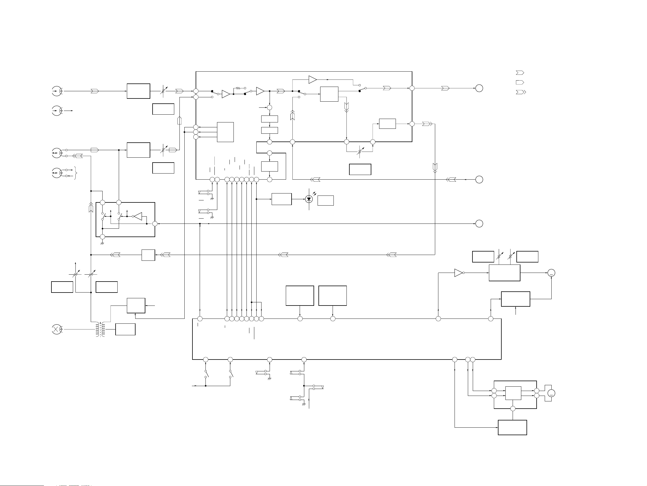
7-3. BLOCK DIAGRAM – MAIN Section –
HCD-CP2
(Page 20)
VIDEO IN
(Page 22)
(Page 19)
AM
MD IN
FM 75Ω
B
E
A
PB-L
PJ303 (1/2)
L
R
L
R
TUNER ON
CD-LCH
ANTENNA
R-CH
R-CH
05
TUNER PACK
FM ANT
ANT GND
ANT GND
AM ANT
MUTING
Q102, 103
L-CH
R-CH
FM-DET
TUNED
DO
DI
CE
CK
R-CH
REC-L
INPUT SELECT SWITCH,
TONE CONTROL,
ELECTRICAL VOLUME
IC301
TAPE-L
12
MD-L
11
CD-L
VIDEO-L
14
TU-L
13
MUTING
Q106
R-CH
2
3
10
11
8
9
4
5
R-CH
BAND-PASS
FILTER
Q830
(AEP, UK, North European)
RDS DECODER
MUX
4
XI XO
13 14
IC803
RDATA
RCLK
X803
4.332MHz
2
16
MO-L
15
INPUT SELECT SWITCH
SDA
SCL
130
SDA
71
SCK
70
TU-DATA
20
TU-CE
23
22
TU-COUNT
21
TU-CLK
RDS-DATA
24
RDS-CLK
61
19
TU-TUNED
VOLUME
IN-L
CONTROL
16
CIRCUIT
SYSTEM CONTROLLER
IC802 (3/4)
TONE
CONTROL
CIRCUIT
VIDEO
AU MUTE
AMP-STBY
AMP-MUTE
SPEAK RELAY
TEX
XTAL1
EXTAL1
MD
LOUT
ATT
ROUT
CONTROL SWITCH
56
60
2
6
5
CONTROL SWITCH
X800
32.768kHz
X801
4.19MHz
74
34
TX
35
32
31
6
5
MUTING
Q317, 318
MUTING
Q303, 304
LINE AMP
IC302
R-CH
D304
MUTING
Q101
R-CH
LED DRIVE
Q815
LED DRIVE
Q869
D812
D821
VIDEO
SPEAKER ON/OFF
SWITCH
Q335, 337
MD
3
POWER AMP
IC101
IN+
STBY
9 10
OUT
MUTE
14
R-CH
R-CH
OVER LOAD
DETECT
Q331, 332
SPEAKER PROTECT
RELAY DRIVE
Q333, 336
MUTING
Q120
R-CH
RY101
R-CH
R-CH
R-CH
SJ301
SPEAKER
IMPEDANCE
USE 6-16Ω
C
(Page 20)
L
PJ303 (2/2)
LINE OUT
R
J301
PHONES
+
L
–
–
R
+
65
66 6 10
45
TRAY-SW
DISC TRAY OPEN/CLOSE
MOTOR DRIVE
IC309
INPUT1TRAY-OPEN
5 2
OUT1
INPUT2TRAY-CLOSE
OUT2
(DISC TRAY CLOSE DET)
(DISC TRAY OPEN DET)
2121
M
M901
DISC TRAY
OPEN/CLOSE
S901
S902
• SIGNAL PATH
: TUNER (FM/AM)
: CD PLAY
: TAPE PLAY
: RECORD
R-CH : Same as L-CH
Page 22

HCD-CP2
7-4. BLOCK DIAGRAM – DISPLAY/POWER SUPPLY Section –
REC/PB
D
(Page 20)
LIQUID CRYSTAL
DISPLAY
LCD801
D811
DSG
D810
CD SYNC
LCD DRIVER
IC800
CAD
SCK
S0 – S31
1–12, 34–41, 42–48, 50–55
30 – 33
RESET
COM0 – COM3
REMOTE CONTROL
RECEIVER
IC804
RV801
VOLUME
S800 – 815, 817 – 833
26
CS
24
SI
23
22
27
LED DRIVE
Q808
LED DRIVE
Q807
ROTARY
ENCODER
RV801
05
26
27
28
29
47
53
59
56
57
46
40 – 44
C/D
LCD DATA
LCD CLK
LCD CE
LCD-XRST
DSG
CD SYNC
REMOCON
JOG-A
JOG-B
KEY1 – KEY5
SYSTEM CONTROLLER
IC802 (4/4)
RESET
REG-CON
TAPE
RDS-ON
TUNER
30
64
48
25
CD
50
49
D807
D806
LED DRIVE
LED DRIVE
LED DRIVE
Q813
Q810
Q811
D817
TAPE
D813
CD
D814
TUNER
D657 – 660
(LCD BACK LIGHT)
CASSETTE HOLDER
BACK LIGHT
D820
STANDBY
(DISC TRAY ILLUMINATION)
REGULATOR
CONTROL SWITCH
Q315, 316
REGULATOR
CONTROL SWITCH
Q311, 312
REGULATOR
CONTROL SWITCH
Q321, 322
BACK UP +5V
SYSTEM CONTROLLER (IC802) B+
RESET SIGNAL
GENERATOR
IC801
D808
D809
Q806
LED DRIVE
I/1
D823
TDA7439 (IC301) B+
TRIGGER MOTOR DRIVE (IC402) B+
Q814
FM 7.5V
FM CIRCUIT B+
RDS DECODER
(IC803) B+
CD BLOCK B+
+12V
RELAY B+
+9.5V
TUNER BLOCK B+
LED B+
+5V
B+ SWITCH
Q804, 805
B+ SWITCH
Q850, 851
Q812
D315
D804
B+ SWITCH
Q800, 801
REGULATOR
REGULATOR
REGULATOR
SWITCHING
Q323, 324
+7.5V
Q314
+5V
Q310
+9.5V
Q313
+5.6V
REGULATOR
IC310
(Saudi Arabia, Singapore)
POWER AMP
(IC101, 201)
(AEP, UK, North European, Australian)
POWER TRANSFORMER
(SUB)
T902
RECT
D903 – 906
POWER TRANSFORMER
(MAIN)
T901
B+
B–
RECT
D907 – 910
RY901
AEP, UK, North European,
Australian
CD BLOCK, DISC TRAY OPEN/
CLOSE MOTOR DRIVER (IC309) B+
22
+8V
22
AUDIO
CIRCUIT
+8V
–8V
+8V
REGULATOR
IC311
+8V
REGULATOR
IC304
–8V
REGULATOR
IC305
+12V
REGULATOR
IC306
RECT
D911 – 914
VOLTAGE
SELECTOR
S901
(Saudi Arabia, Singapore)
TUNER ON
AC IN
E
(Page 21)
Page 23

HCD-CP2
d
• Circuit Boards Location
LEAF SWITCH board
LCD board
CONTROL board
HEADPHONE board
AUDIO board
POWER board
TUNER board
AMP boar
7-5. NOTE FOR PRINTED WIRING BOARDS AND SCHEMATIC DIAGARAMS
Note on Printed Wiring Board:
• X : parts extracted from the component side.
• Y : parts extracted from the conductor side.
• x : parts mounted on the conductor side.
• b : Pattern from the side which enables seeing.
(The other layers' patterns are not indicated.)
Note on Schematic Diagram:
• All capacitors are in µF unless otherwise noted. pF: µµF
50 WV or less are not indicated except for electrolytics
and tantalums.
• All resistors are in Ω and 1/
specified.
• 5 : fusible resistor.
Note: The components identified by mark 0 or dotted line
with mark 0 are critical for safety.
Replace only with part number specified.
• U : B+ Line.
• V : B– Line.
• H : adjustment for repair.
• Voltages are tak en with a V OM (Input impedance 10 MΩ).
Voltage variations may be noted due to normal production tolerances.
• Waveforms are taken with a oscilloscope.
Voltage variations may be noted due to normal production tolerances.
• Circled numbers refer to waveforms.
• Signal path.
F : TUNER (FM/AM)
E : PLAYBACK (DECK A)
d : PLAYBACK (DECK B)
a :RECORD
J : CD PLAY (ANALOG OUT)
c : CD PLAY (DIGITAL OUT)
• Abbreviation
AUS : Australian model
AED : North European model
EA : Saudi Arabia model
SP : Singapore model
4
W or less unless otherwise
LOADING board
MAIN board
CD board
2323
Page 24

HCD-CP2
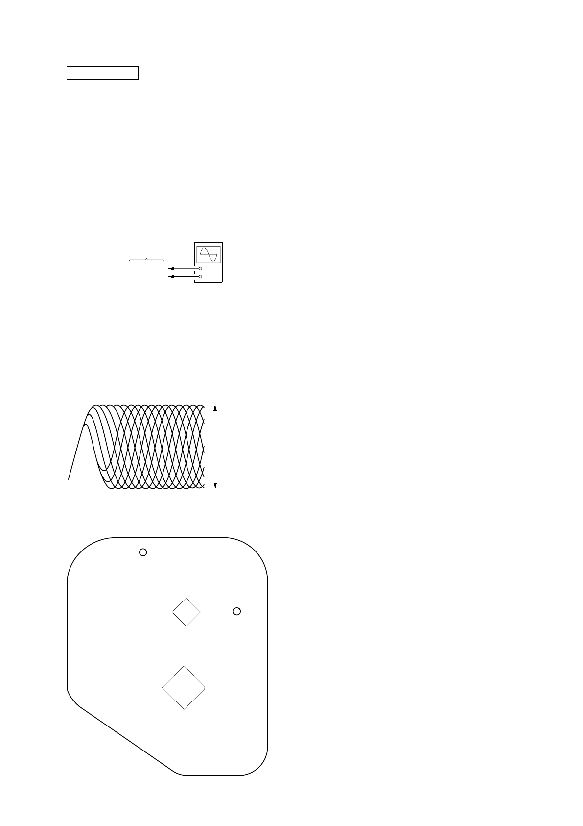
7-6. PRINTED WIRING BOARD – CD Section – • See page 23 for Circuit Boards Location.
• Semiconductor
Location
Ref. No. Location
IC701 C-5
IC702 C-2
IC703 F-5
Q701 B-6
(Page 28)
24
24
Page 25

7-7. SCHEMATIC DIAGRAM – CD Section – • See pag e 30 for Wavef orms. • See page 39 for IC Block Diagrams.
HCD-CP2
• Voltages and waveforms are dc with respect to ground
under no-signal conditions.
no mark : CD PLAY
The components identified by mark 0 or dotted
line with mark 0 are critical for safety.
Replace only with part number specified.
: Impossible to measure
∗
(Page 32)
2525
Page 26

HCD-CP2
( )
–
+
05
TO
AUDIO
BOARD
7-8. PRINTED WIRING BOARDS – TAPE DECK Section – • See page 23 for Circuit Boards Location.
(
)
( )
(Page 28)
B
TO
MOTOR
BOARD
( )
B
C
E
05
(DECK A PLAY)
05
(DECK A HALF)
(DECK A 120/70)
CB
(DECK A REC) (DECK B HALF)
CB
CB
c
(Page 28)
(DECK B PLAY)
(DECK B 120/70)(DECK B REC)
26
26
Page 27

7-9. SCHEMATIC DIAGRAM – TAPE DECK Section – • See page 30 for Waveform. • See page 42 for IC Block Diagram.
HCD-CP2
(Page 31)
(Page 31)
BMETAL
• Voltages and wavefor ms are dc with respect to ground
under no-signal conditions.
no mark : TAPE PLAY
( ) : RECORD
The components identified by mark 0 or dotted
line with mark 0 are critical for safety.
Replace only with part number specified.
2727
Page 28

HCD-CP2
• Semiconductor
Location
Ref. No. Location
D301 C-7
D304 H-5
D314 I-9
D315 B-8
D317 B-9
D318 H-9
D319 B-7
D320 G-7
D321 G-7
D322 E-5
D323 C-7
D324 D-5
D325 D-5
D330 I-5
D331 I-5
D804 F-1
D805 B-6
D806 I-5
D807 I-5
D808 I-6
D809 I-6
D815 I-5
D816 F-1
7-10. PRINTED WIRING BOARD – MAIN Board – • See page 23 for Circuit Boards Location.
(Page 29)
(Page 29)
(Page 29)
(Page 26)
IC301 D-7
IC302 C-9
IC304 I-9
IC305 I-7
IC306 I-9
IC308 E-9
IC309 C-5
IC310 H-9
IC311 I-8
IC401 G-8
IC402 F-9
IC800 F-3
IC801 H-2
IC802 I-2
IC803 B-5
Q101 C-9
Q102 D-9
Q103 D-9
Q106 B-9
Q201 C-9
Q202 D-9
Q203 D-9
Q206 A-9
Q303 I-5
Q304 I-5
Q310 I-9
Q311 I-9
Q312 I-9
Q313 B-9
Q314 B-8
Q315 B-8
Q316 B-8
Q317 H-5
Q318 H-5
Q321 B-9
Q322 B-9
Q323 H-9
Q324 H-9
Q403 F-9
Q406 G-9
Q407 G-9
Q408 F-9
Q409 G-9
Q800 I-7
Q801 I-7
Q804 I-6
Q805 I-7
Q806 I-6
Q830 B-6
Q850 I-6
Q851 I-5
(Page 26)
(Page 24)
(Page 36)
(Page 34)
28
28
(Page 38)
Page 29

7-11. PRINTED WIRING BOARDS – LCD/LOADING Boards –
M
M901
DISC TRAY
OPEN/CLOSE
S901
DISC TRAY
CLOSE DET
S902
DISC TRAY
OPEN DET
CN900
1
5
11
1-640-523-
F
LOADING BOARD
05
• See page 23 for Circuit Boards Location.
CN804
CN802
(Page 28)(Page 28)
(Page
28)
29
Page 30

• Wavef orms
p
– CD Board –
– MAIN Board –
1 IC701 1 (FEO) (CD Play Mode)
2 IC701 ed (RF O), IC703 eg (RF)
(CD Play Mode)
3 IC701 rg (TEO) (CD Play Mode)
Approx.
200 mVp-p
1.2 ± 0.1 Vp-p
6 IC703 rd (BCK) (CD Play Mode)
472 ns
7 IC703 u; XTAI (CD Play Mode)
16.9344 MHz
6.4 Vp-p
4.3 Vp-p
1 IC802 es (XTAL1)
5.2 Vp-p
4.19 MHz
2 IC802 ef (TX)
5.2 Vp-p
32.768 kHz
3 IC803 qd (XI)
Approx.
100 mVp-p
4 IC703 wa (MDP) (CD Play Mode)
2.8 Vp-
7.6 µs
5 IC703 el (LRCK) (CD Play Mode)
6.6 Vp-p
– AUDIO Board –
1 Q621, 622 (Collector)
(Record Mode)
11.3 µs
18.4 Vp-p
2.9 Vp-p
4.332 MHz
4 IC803 qh (RCLK)
4.4 Vp-p
840 µs
30
22.8 µs
Page 31

7-12. SCHEMATIC DIAGRAM – MAIN Section (1/3) – • See page 42 for IC Block Diagrams.
HCD-CP2
(Page 27)
(Page 27)
(Page 32)
(Page 33)
• Voltages are dc with respect to ground under no-signal
(detuned) conditions.
no mark : TUNER (FM/AM)
( ) : CD PLAY
{ } : TAPE PLAYBACK (DECK A)
[ ] : TAPE PLAYBACK (DECK B)
〈〈 〉〉 : RECORD
< > : MD/VIDEO
3131
Page 32

HCD-CP2
7-13. SCHEMATIC DIAGRAM – MAIN Section (2/3) – • See page 43 for IC Block Diagram.
(Page 35)
(Page 38)
(Page 31)
(Page
33)
(Page 33)
(Page 33)
(Page 33)
(Page 25)
32
(Page 33)
32
• Voltages are dc with respect to ground under no-signal
(detuned) conditions.
no mark : TUNER (FM/AM)
( ) : CD PLAY
{ } : TAPE PLAYBACK (DECK A)
[ ] : TAPE PLAYBACK (DECK B)
〈〈 〉〉 : RECORD
< > : MD/VIDEO
Page 33

7-14. SCHEMATIC DIAGRAM – MAIN Section (3/3) – • See page 30 for Waveforms. • See page 43 for IC Block Diagram.
HCD-CP2
(Page 32)
(Page 32)
(Page 32)
(Page
32)
(Page 31)
(Page 32)
(Page 37)
• Voltages and wavefor ms are dc with respect to ground
under no-signal (detuned) conditions.
no mark : TUNER (FM/AM)
( ) : CD PLAY
{ } : TAPE PLAYBACK (DECK A)
[ ] : TAPE PLAYBACK (DECK B)
〈〈 〉〉 : RECORD
< > : MD/VIDEO
3333
Page 34

HCD-CP2
7-15. PRINTED WIRING BOARDS – AMP/HEADPHONE Boards – • See page 23 for Circuit Boards Location.
• Semiconductor
Location
Ref. No. Location
D311 D-1
IC101 B-4
IC201 B-5
Q120 E-2
Q220 E-3
Q331 D-2
Q332 D-1
Q333 D-1
Q335 E-2
Q336 D-2
Q337 E-2
TO
AMP
BOARD
L305
L304
L306
JR103
(Page 38)
(Page 28)
TO HEADPHONE
BOARD
34
34
Page 35

7-16. SCHEMATIC DIAGRAM – POWER AMP Section – • See page 43 for IC Block Diagram.
HCD-CP2
(Page 32)
(Page 38)
• Voltages are dc with respect to ground under no-signal
(detuned) conditions.
no mark : TUNER (FM/AM)
( ) : CD PLAY
{ } : TAPE PLAYBACK (DECK A)
[ ] : TAPE PLAYBACK (DECK B)
〈〈 〉〉 : RECORD
< > : MD/VIDEO
3535
Page 36

HCD-CP2
7-17. PRINTED WIRING BOARD – CONTROL Board – • See page 23 for Circuit Boards Location.
• Semiconductor
Location
Ref. No. Location
D810 A-3
D811 B-5
D812 C-7
D813 C-6
D814 C-5
D817 C-6
D820 B-8
D821 C-7
D822 A-6
D823 D-6
IC804 D-8
Q807 A-4
Q808 C-4
Q809 C-7
Q810 C-6
Q811 C-5
Q812 B-7
Q813 C-6
Q814 C-8
Q815 C-7
Q816 B-6
(Page 28)
36
36
Page 37

7-18. SCHEMATIC DIAGRAM – KEY CONTROL Section –
HCD-CP2
(Page 33)
• Voltages are dc with respect to ground under no-signal
(detuned) conditions.
no mark : TUNER (FM/AM)
3737
Page 38

HCD-CP2
7-19. PRINTED WIRING BOARD – POWER Board –
• See page 23 for Circuit Boards Location.
(Page 28)
(Page 34)
7-20. SCHEMATIC DIAGRAM – POWER SUPPLY Section –
(Page 35)
(Page 32)
• Semiconductor
Location
Ref. No. Location
D902 E-3
D903 B-2
D904 B-2
D905 A-2
D906 A-2
D907 A-5
D908 A-5
D909 B-5
D910 B-5
D911 A-3
D912 A-3
D913 A-2
D914 A-2
The components identified by mark 0 or dotted
line with mark 0 are critical for safety.
Replace only with part number specified.
38
38
Page 39

• IC Block Diagrams
FZC
VC
TDFCT
TZC
ATSC
TEI
LPFI
TEO
VEE
EI
E
F
FE
BIAS
SL P
SL M
SL O
ISET
VCC
XRST
DATA
XLT
CLK
LOCK
SENS2
SENS1
C. OUT
VCC
DFCTO
IFB1 – IFB6
BAL1 – BAL4
TOG1 – TOG4
FS1 – FS4
TG1 – TG2
TM1 – TM7
PS1 – PS4
TGH
TGL
BALH
BALL
ATSC
DFCT
TM1
TG1
FS2
IFB1 – IFB6
VCC
VEE
VCC
VEE
VEE
PD 2
I-V AMP
FOK
CC2
CC1
CB
CP
RF O
RF I
RFTC
PD2
PD1
PD
LD
RF M
TA O
TA M
FSET
TG2
TGU
SRCH
FEO
FEI
FDFCT
FGD
FLB
FE O
FE M
TZC
FZC
FOL
FOH
MIRR
LDON
LPCL
LPC
TGFL
DFCT1
CC1
1 2 3
4
5
6
7
8 9 10
26
25
24
23
22
21
20
19
18
17
16
15
14
40
41
42
43
44
45
46
47
48
49
50
51
52
39
PD 1
I-V AMP
38
PD
AMP
37
LD
AMP
LASER
POWER
CONTROL
FOCUS BIAS
WINDOW
COMPARATOR
FOCUS ERROR
AMP
F I-V
AMP
E I-V
AMP
TGFL
TRACKING GAIN
WINDOW
COMPARATOR
E-F BALANCE
WINDOW
COMPARATOR
ATSC
WINDOW
COMPARATOR
TZC
COMPARATOR
TRACKING PHASE
COMPENSATION
CENTER
VOLTAGE
GENERATOR
FZC
COMPARATOR
FOCUS PHASE
COMPENSATION
CHARGE UP
FSET
ISET
IIC DATA REGISTER, INPUT SHIFT REGISTER,
ADDRESS DECODER, SENSE SELECTOR,
OUTPUT DECODER
TTL
↓
IIL
IIL
↓
TTL
IIL
↓
TTL
RF SUMMING
AMP
FOCUS OK
COMPARATOR
PEAK/BOTTOM
HOLD
PEAK/BOTTOM
HOLD
DEFECT
AMP
MIRR
COMPARATOR
36 34 31 30 29 28 27
35
33 32
BAL1 – BAL4
TM6
TM2
VCC
VEE
TM5
11 12 13
TG2
TM4
VCC
VEE
TM3
FS1
VCC
VEE
TOG1 – TOG4
TM7
FS4
DFCT
+
–
+
–
– CD Board –
IC701 CXA1992BR
39
Page 40

IC702 BA6898FP-E2
GND
OUT4-B
OUT4-A
IN4
28 27 26 25 24 22 21 20 19 18 17 16
IN4,VREF INVCC
VCC VCC
VCC
IN3,IN3
OUT3-A
OUT3-BNCOPIN-B
1523
NC
LEVEL SHIFT
–
+
+
–
LEVEL SHIFT
1 2 3 4 5 6 7 8 9 10 11 12 13 14
IN1
OUT1-B
OUT1-A
RESET
REG-B
–
+
REGOUT
REGULATOR
BIAS, T. S. D
MONITOR
+
MUTE
–
GND
DRIVER
MUTE
,
IN2
+
–
LEVEL SHIFT
IN2
LEVEL SHIFT
–
+
OUT2-A
GND
OUT2-B
+
OPOUT
–
40
Page 41

IC703 CXD2589Q
VDD
SYSM
AVSS
AVDD
AOUT1
AIN1
LOUT1
AVSS
XVDD
XTAI
XTAO
VSS
61
62
63
64
65
66
67
68
69
70
71
PWM
OSC
PWM
EXCK
SBSO
SCOR
WFCK
SERIAL-IN
INTERFACE
OVER SAMPLING
DIGITAL FILTER
3rd-ORDER
NOISE SHAPER
SUB CODE
PROCESSOR
ENPHI
EMPH
DOUT
C4M
XTSL
C2PO
CORRECTOR
GFS
ERROR
XPCK
XUGF
EFM
DEMODULATOR
VDD
16k
RAM
VSS
BCKI
BCK
PCMDI
45 44 43 42 4150 49 48 47 4655 54 53 52 5159 58 57 5660
PCMD
ASYMMETRY
CORRECTOR
DIGITAL
PLL
40
LRCKI
39
LRCK
38
ASYO
ASYI
37
BIAS
36
RF
35
AVDD
34
CLTV
33
AVSS
32
31
FILI
FILO
30
PCO
29
XVSS
AVSS
LOUT2
AIN2
AOUT2
AVDD
AVSS
XRST
VDD
DIGITAL
72
73
74
75
76
77
78
79
80
1 2 3 4 5 6 12 13 14 15 16 17 19 20
VSS
LMUTE
RMUTE
OUT
CPU
INTERFACE
7 8 9 10 11 18
SQCK
SQSO
SENS
DATA
XLAT
CLOK
SEIN
D/A
INTERFACE
CLOCK
GENERATOR
SERVO
AUTO
SEQUENCER
CNIN
DATO
XLTO
CLKO
SPOA
SPOB
XLON
FOK
VDD
VSS
OSC
DIGITAL
CLV
28
V16M
VCTL
27
VCKI
26
VPCO1
25
TES1
24
TES0
23
PWMI
22
21
MDP
41
Page 42

– AUDIO Board –
IC602 µPC1330HA
2
1
SW R1 GND SW P1
3
– MAIN Board –
IC301 TDA7439
4
CONT
INVERTER
COMPARATER
5
VCC
GND
6
SW P2 GND
7 8 9
SW R2
SCL
DIG GND
TREBLE (R)
TREBLE (L)
MIN (L)
MOUT (L)
BOUT (L)
BIN (L)
BOUT (R)
BIN (R)
MOUT (R)
IIC BUS
DECODER &
LATCH
VREF
SUPPLY
1 2 3 4 5 6
CREF
VS
AGND
SDA
MIN (R)
ROUT
LOUT
INR
18
VOLUME
TREBLE
MIDDLE
BASS
SPEAKER
ATTENUATOR
MUX OUT (R)
GAIN AMP
MULTIPLEXER
7 8
9 10
R-IN4
R-IN3
R-IN2
R-IN1
161727282930 22 21 20 1926 25 24 23
VOLUME
TREBLE
MIDDLE
BASS
SPEAKER
ATTENUATOR
GAIN AMP
MULTIPLEXER
11 12
13 14
L-IN1
L-IN2
INL
L-IN3
15
L-IN4
42
MUX OUT (L)
Page 43

IC309, 402 KA3082 IC803 BU1924F-E2 (AEP, UK, North European models)
VDD2
XI
DIGITAL
BIAS
GND
OUT1
DRIVER OUT
PRE DRIVER
VZ1
VCTL
LOGIC
SWITCH
5 6 7 8 9 101 2 3 4
IN1
IN2
VCC1
TSD
VCC2
VZ2
OUT2
RCLK
1187.5Hz
PLL
BIPHASE
DECODER
NC
PLL 57kHz
RDS/ARI
COMPARATOR
8th SWITCHED
CAPACITOR
FILTER
XO
141516 13 121110 9
CLOCK
VSS2
T1
TEST
T2
– AMP Board –
IC101, 201 TDA7296
BIPOLAR
TRANSCONDACTANCE
INPUT STAGE
–
+
IN+
NC
IN+ MUTE
IN–
STBY-GND
MOS GAIN &
LEVEL SHIFTING
STAGE
BOOST-
STRAP
BOOSTSTRAP
+VS
STANDBY/
MUTE
–VS
STBY
THERMAL
SHUTDOWN
MOS
OUTPUT
STAGE
MUTE
SHORT
CIRCUIT
PROTECTION
NC
NC
14 1512 1310 118 96 753 41 2
OUT
+PWVS
DEFFERENTIAL
1 43 65 872
QUAL
–PWVS
DECODER
RDAT
ANTI-ALIASING
VREF
FILTER
MUX
ANALOG
VDD1
VSS1
VSS3
CMP
43
Page 44

7-21. IC PIN FUNCTION DESCRIPTION
• MAIN BOARD IC802 CXP84332-168Q (SYSTEM CONTROLLER)
Pin No. Pin Name I/O Description
1 A/B O Deck-A/B selection signal output to the HA12203NT (IC401) “L”: deck-A, “H”: deck-B
2 AMP-STBY O Standby on/off control signal output to the power amplifier (IC101, 201) “L”: standby mode
3 HI DUB REC O High speed dubbing control signal output to the HA12203NT (IC401)
4 C-XRST O Reset signal output to the CXA1992BR (IC701) and CXD2589Q (IC703) “L”: reset
5 SPEAK RELAY O Speaker protect relay drive signal output terminal “H”: relay on
6 AMP-MUTE O Muting on/off control signal output to the power amplifier (IC101, 201) “H”: muting on
7 REC-BIAS O
Recording bias on/off selection signal output to the HA12203NT (IC401)
“L”: bias on, “H”: bias off
8 REC/PB O
CAP MOTOR
9
10
11
12
13
14 T-HALF (A) I
15 T-PLAY (A) I Detection input from the deck-A play detect switch (S1001) “H”: deck-A play
16 TC-SHUT (A) I Shut off detection signal input from the deck-A side reel pulse detector (Q1001)
17 TC-SHUT (B) I Shut off detection signal input from the deck-B side reel pulse detector (Q1002)
18 T-PLAY (B) I Detection input from the deck-B play detect switch (S1002) “H”: deck-B play
19 TU-TUNED I Tuning detection signal input from the tuner pack “L”: tuned
20 TU-DATA O PLL serial data output to the tuner pack
21 TU-CLK O PLL serial data transfer clock signal output to the tuner pack
22 TU-COUNT I PLL serial data input from the tuner pack
23 TU-CE O PLL chip enable signal output to the tuner pack
24 RDS-DATA I
CON
CAP MOTOR
H/L
TRIG MOTOR
CON (A)
TRIG MOTOR
CON (B)
TRIG MOTOR
H/L
Recording/playback/pass selection signal output to the HA12203NT (IC401)
“L”: recording mode, “H”: pass, “Hi-z”: playback mode
O Capstan motor on/off control signal output terminal “H”: motor on
High/normal speed selection signal output of the capstan motor
O
“L”: normal speed, “H”: high speed
Deck-A side trigger motor drive signal output to the trigger motor drive (IC402)
O
“H”: motor on
Deck-B side trigger motor drive signal output to the trigger motor drive (IC402)
O
“H”: motor on
O Trigger motor control signal output terminal
Detection input from the deck-A cassette detect switch (S1003)
“L”: cassette in, “H”: no cassette
RDS serial data input from the RDS decoder (IC803)
(Used for the AEP, UK and North European models only)
25 RDS-ON O
26 C/D O Command data output to the liquid crystal display driver (IC800)
27 LCD DATA O Serial data output to the liquid crystal display driver (IC800)
28 LCD CLK O Serial data transfer clock signal output to the liquid crystal display driver (IC800)
29 LCD CE O Chip enable signal output to the liquid crystal display driver (IC800)
30 RESET I
31 EXTAL1 I Main system clock input terminal (4.19 MHz)
32 XTAL1 O Main system clock output terminal (4.19 MHz)
33 VSS — Ground terminal
34 TX O Sub system clock output terminal (32.768 kHz)
35 TEX I Sub system clock input terminal (32.768 kHz)
36 AVSS — Ground terminal (for A/D converter)
Power supply on/off control signal output of the tuner pack (+7.5V) and RDS decoder (IC803)
(Used for the AEP, UK and North European models only)
System reset signal input from the reset signal generator (IC801) “L”: reset
For several hundreds msec. after the power supply rises, “L” is input, then it changes to “H”
44
Page 45

Pin No. Pin Name I/O Description
e
37 AVREF I Reference voltage (+5V) input terminal (for A/D converter)
38 SIMUKE I Destination setting terminal (A/D input)
39 T-MODE I Detection input from the deck-B half detect switch (S1006)
40 KEY1 I
Key input terminal (A/D input)
S800 to S807 (TUNING –/+, REC z, TAPE B m/M/x/Y, TUNER BAND keys input)
41 KEY2 I
42 KEY3 I
43 KEY4 I
Key input terminal (A/D input) S808 to S815 (CD x/u, TUNING MODE, REPEAT, PLAY
MODE,CD . m/> M, EJECT Z keys input)
Key input terminal (A/D input)
S817 to S823 (DSG, VIDEO, MD, TAPE, CD, TUNER, STANDBY I/1 keys input)
Key input terminal (A/D input)
S824 to S831 (X, CD SYNC, HI-SPEED DUBBING, TAPE A m/M/x/Y keys input)
44 KEY5 I Key input terminal (A/D input) S832 and S833 (BASS, TREBLE keys input)
45 TRAY-SW I
Disc tray position detect switch (S901, S902) input terminal (A/D input)
“L”: close position, “M”: open position, “H”: moving
46 JOG-B I Jog dial pulse input from the rotary encoder (RV801 VOLUME) (B phase input)
47 LCD-XRST O Reset signal output to the liquid crystal display driver (IC800) “L”: reset
48 TAPE O
49 TUNER O
50 CD O
Power supply on/off control signal output of the cassette holder back light
LED drive signal output of the TAPE indicator (D817) “H”: back light on (LED on)
Power supply on/off control signal output of the tuner pack (+9.5V)
LED drive signal output of the TUNER indicator (D814) “H”: tuner power on (LED on)
Power supply on/off control signal output of the CD block (+5V)
LED drive signal output of the CD indicator (D813) “H”: CD power on (LED on)
51 C-SQCK O Subcode Q data reading clock signal output to the CXD2589Q (IC703)
52 C-SQSO I Subcode Q data input from the CXD2589Q (IC703)
53 DSG O
LED drive signal output of the DSG (Dynamic Sound Generator) indicator (D811)
“H”: LED on
54 CD-SENS1 I
Internal status detection monitor input from the CXD2589Q (IC703)
(for FZC, DFCT1, TZC, etc.)
55 SENS2 I Internal status detection monitor input from the CXA1992BR (IC701) (for MIRR, DFCT2, etc.)
56 REMOCON I Sircs remote control signal input from the remote control receiver (IC804)
57 JOG-A I Jog dial pulse input from the rotary encoder (RV801 VOLUME) (A phase input)
MD function control signal output terminal
58 MD O
LED drive signal output of the MD indicator (D812)
“H”: MD (LED on) (“L” output when other functions)
59 CD SYNC O LED drive signal output of the CD SYNC indicator (D810) “H”: LED on
VIDEO function control signal output terminal
60 VIDEO O
LED drive signal output of the VIDEO indicator (D821)
“H”: VIDEO (LED on) (“L” output when other functions)
61 RDS-CLK I
Serial data reading clock signal input from the RDS decoder (IC803)
(Used for the AEP, UK and North European models only)
62 C-SCOR I Subcode sync (S0+S1) detection signal input from the CXD2589Q (IC703)
63 WP I Wake up control signal input terminal
64 REG-CON O Main system power supply on/off control signal output terminal “H”: power on
65 TRAY-OPEN O Motor drive signal output to the disc tray open/close motor drive (IC309) “H” active *1
66 TRAY-CLOSE O Motor drive signal output to the disc tray open/close motor drive (IC309) “H” active *1
*1 Disc tray open/close motor (M901) control
Mod
Terminal
TRAY-OPEN (pin yg )
TRAY-CLOSE (pin yh )
Stop Table In Table Out Brake
“L”“L”“H”“H”
“L”“H”“L”“H”
45
Page 46

Pin No. Pin Name I/O Description
67 C-XLAT O Serial data latch pulse output to the CXD2589Q (IC703)
68 REC/PB O
69 C-MUTE O Muting on/off control signal output to the CXD2589Q (IC703)
70 SCK O Serial data transfer clock signal output to the TDA7439 (IC301)
71 SDA O
72 VDD — Power supply terminal (+5V)
73 NC — Connected to power supply (+5V)
74 AU MUTE O Muting on/off control signal output terminal “H”: muting on
75 LINE MUTE O
76 C-CLK O Serial data transfer clock signal output to the CXD2589Q (IC703)
77 C-DATA O Serial data output to the CXD2589Q (IC703)
78 DOLBY O
Recording/playback selection signal output to the REC/PB switching (IC602)
“L”: playback mode, “H”: recording mode
Serial data output to the TDA7439 (IC301)
Line muting on/off selection signal output to the HA12203NT (IC401)
“L”: muting off, “H”: muting on
Dolby NR on/off selection signal output to the HA12203NT (IC401)
“L”: dolby off, “H”: dolby on
79 REC-MUTE O
80 NORMAL/HI O
Recording muting on/off selection signal output to the HA12203NT (IC401)
“L”: muting off, “H”: muting on
Normal/high speed selection signal output to the HA12203NT (IC401)
LED drive signal output of the HI-SPEED DUBBING indicator (D822)
“L”: normal speed, “H”: high speed (LED on)
46
Page 47

SECTION 8
3
4
1
2
6
5
6
#1
#2
#2
#1
#1
#1
#1
#3
TCM-220WR2E
7
EXPLODED VIEWS
NOTE:
• -XX and -X mean standardized parts, so they
may have some difference from the original
one.
• Color Indication of Appearance Parts
Example:
KNOB, BALANCE (WHITE) . . . (RED)
↑↑
Parts Color Cabinet's Color
• Abbreviation
AUS : Australian model
AED : North European model
EA : Saudi Arabia model
SP : Singapore model
(1) GENERAL SECTION
• Items marked “*” are not stocked since they
are seldom required for routine service. Some
delay should be anticipated when ordering
these items.
• The mechanical parts with no reference number in the exploded views are not supplied.
• Hardware (# mark) list is given in the last of
the electrical parts list.
The components identified by
mark 0 or dotted line with mark
0 are critical for safety.
Replace only with part number
specified.
Ref. No. Part No. Description Remark
1 4-222-365-01 SPRING (CASSETTE B)
2 4-222-364-01 SPRING (CASSETTE A)
3 X-4951-962-1 HOLDER (A) SUB ASSY, CASSETTE
4 X-4951-963-1 HOLDER (B) SUB ASSY, CASSETTE
Ref. No. Part No. Description Remark
5 4-222-370-01 COVER (UPPER)
6 4-221-580-01 SCREW, CASE
7 3-831-441-99 SPACER
47
Page 48

(2) FRONT PANEL SECTION
d
54
55
56
53
60
57
62
59
58
63
#1
64
65
#2
67
63
70
#1
62
66
#1
69
not supplie
69
69
52
51
supplied with
RV801
Ref. No. Part No. Description Remark
51 X-4952-108-1 KNOB ASSY
52 4-222-401-01 BUTTON (BASS)
53 X-4951-956-1 PANEL SUB ASSY, FRONT (AEP, UK, AED)
53 X-4952-135-1 PANEL SUB ASSY, FRONT (EA, SP, AUS)
54 4-222-362-01 WINDOW (CASSETTE)
55 4-222-368-01 SHEET (CASSETTE)
56 4-222-363-01 LID, CASSETTE
57 1-791-437-11 WIRE (FLAT TYPE) (17 CORE)
58 1-791-438-11 WIRE (FLAT TYPE) (21 CORE) (180mm)
59 1-675-150-11 LCD BOARD
68
Ref. No. Part No. Description Remark
61 4-222-376-01 BRACKET (LCD)
62 1-418-482-11 ILLUMINATION BLOCK, LED
63 4-222-388-01 SPRING (CASSETTE LID)
64 4-222-394-01 BRACKET (CASSETTE LID A)
65 4-222-395-01 BRACKET (CASSETTE LID B)
66 1-791-435-11 WIRE (FLAT TYPE) (21 CORE) (105mm)
67 A-4426-637-A CONTROL BOARD, COMPLETE
68 4-218-204-01 FOOT (FRONT)
69 4-931-757-31 SCREW (DIA.2.6X8) (IT3B), TAPPING
70 1-675-153-11 HEADPHONE BOARD
60 4-217-319-01 PLATE, LCD LIGHT
48
Page 49

(3) CHASSIS SECTION
102
113
#4
#4
103
114
UK
115
#1
#1
#1
#1
not supplied
101
T901
#1
#1
not
supplied
104
#1
112
not
supplied
110
111
#1
107
109
#1
108
106
#1
105
not
supplied
#1
#1
Ref. No. Part No. Description Remark
101 4-222-377-01 CHASSIS (LOWER)
102 1-675-155-11 POWER BOARD
103 4-222-361-01 PANEL, BACK (AEP, UK, AED)
103 4-222-361-21 PANEL, BACK (EA, SP)
103 4-222-361-31 PANEL, BACK (AUS)
104 1-675-154-11 RETAINER BOARD
105 A-4426-641-A MAIN BOARD, COMPLETE (AEP, UK, AED)
105 A-4426-844-A MAIN BOARD, COMPLETE (EA, SP)
105 A-4428-617-A MAIN BOARD, COMPLETE (AUS)
106 A-4411-460-A TUNER PACK (AEP, UK, AED)
106 A-4426-617-A TUNER PACK (EA, SP, AUS)
107 A-4426-642-A AMP BOARD, COMPLETE (AEP, UK, AED)
107 A-4426-842-A AMP BOARD, COMPLETE (EA, SP)
The components identified by mark 0 or dotted
line with mark 0 are critical for safety.
Replace only with part number specified.
Ref. No. Part No. Description Remark
107 A-4473-065-A AMP BOARD, COMPLETE (AUS)
108 1-791-436-11 WIRE (FLAT TYPE) (21 CORE)
109 1-791-434-11 WIRE (FLAT TYPE) (11 CORE)
110 4-931-757-31 SCREW (DIA.2.6X8) (IT3B), TAPPING
* 111 4-217-354-01 BUSHING, INSULATING
112 4-217-355-01 FOOT
113 4-217-332-01 LID, CD
0 114 1-690-608-11 CORD, POWER (WITH CONNECTOR) (AUS)
0 114 1-696-169-11 CORD, POWER
0 115 1-770-019-11 ADAPTOR, CONVERSION PLUG 3P (UK)
0 T901 1-435-100-11 TRANSFORMER, POWER (AEP, UK, AED, AUS)
0 T901 1-435-101-11 TRANSFORMER, POWER (EA, SP)
49
Page 50

(4) CD MECHANISM DECK SECTION-1
(KSL-2130CCP/K1N)
157
158
159
151
not
supplied
not
supplied
152
156
155
154
153
M901
161
not
supplied
160
not
supplied
157
162
not
supplied
164
165
169
167
Ref. No. Part No. Description Remark
* 151 2-646-290-01 TRAY (2130)
152 2-625-541-02 DAMPER (S)
153 2-625-279-01 SCREW (B 2.6X2.5), +
154 2-625-274-02 GEAR, MIDWAY
155 2-625-276-02 PULLEY, LOADING
156 3-653-387-00 BELT, LM
157 2-626-294-01 SCREW (+PTPWH) (2.6X7)
* 158 2-625-284-05 PLATE, CHUCKING
159 1-452-493-21 MAGNET
160 2-625-286-03 PULLEY, CHUCKING
163
165
166
167
#5
165
166
#5
167
#5
Ref. No. Part No. Description Remark
161 3-319-501-51 SCREW (+PTPWH) (2.6X16)
* 162 2-646-288-01 CHASSIS (2130), SUB
* 164 1-640-523-11 LOADING BOARD
* 165 2-627-234-01 INSULATOR
166 2-627-235-01 SPRING (REAR), COIL
167 2-646-289-01 WASHER (2130)
168 2-641-386-01 SCREW (2X5), TAPPING (S)
169 2-627-236-01 SPRING (FRONT), COIL
M901 X-2625-117-1 MOTOR ASSY, LOADING
50
Page 51

(5) CD MECHANISM DECK SECTION-2
(KSL-2130CCP/K1N)
not supplied
203
208
205
206
M702
207
not supplied
202
M701
209
204
201
Ref. No. Part No. Description Remark
201 A-4405-850-A CD BOARD, COMPLETE
202 2-625-188-02 GEAR (A)
203 2-627-003-02 GEAR (B) (RP)
204 1-773-126-11 WIRE (FLAT TYPE) (19 CORE)
205 2-626-908-01 SHAFT, SLED
0 206 8-820-070-02 OPTICAL PICK-UP KSM-213CCP/K1N
#6
The components identified by mark 0 or dotted
line with mark 0 are critical for safety.
Replace only with part number specified.
Ref. No. Part No. Description Remark
207 3-713-786-51 SCREW +P 2X3
208 2-641-386-01 SCREW (2X5), TAPPING (S)
209 1-773-113-11 WIRE (FLAT TYPE) (16 CORE)
M701 X-2646-381-1 MOTOR CHASSIS ASSY (MB) (SPINDLE)
M702 X-2625-769-1 MOTOR GEAR ASSY (MB) (RP) (SLED)
51
Page 52

(6) TAPE MECHANISM DECK SECTION-1
(TCM-220WR2E)
274
275
#8
272
(including z C)
z A
271
HP101
(including z A)
256
255
254
252
251
not supplied
#9
not supplied
257
259
#7
not supplied
not supplied
264
262
258
260
not supplied
HRPE101
(including z B)
253
256
255
254
265
261
273
266
263
267
268
270
264
not supplied
#9
259
271
257
z A
269
265
260
253
262
266
271
261
258
270
z B
263
#9
#8
r B
274
252
#7
251
Ref. No. Part No. Description Remark
251 3-908-560-01 SPRING, AZIMUTH ADJUSTMENT
252 3-919-684-01 SCREW, AZIMUTH ADJUSTMENT
253 X-3373-113-1 SLIDER (HEAD) ASSY
254 3-009-956-11 SPRING, HEAD TOGGLE
255 3-908-558-02 FITTING BLOCK, HEAD
256 3-908-557-02 ROTARY BLOCK, HEAD
* 257 3-908-559-01 STOPPER, AZIMUTH
258 3-908-555-01 SLIDER (REV SLIDER)
259 3-917-143-11 SPRING, TENSION
260 3-388-848-01 SCREW (P2X6) (B TIGHT)
261 3-939-371-01 SPRING (1), TENSION
262 X-3369-909-1 PINCH LEVER (REV) ASSY
263 X-3369-908-1 PINCH LEVER (FWD) ASSY
264 3-908-613-01 GEAR (S), REEL
not supplied
Ref. No. Part No. Description Remark
265 3-917-141-01 SPRING, COMPRESSION
266 X-3371-305-1 REEL (T) ASSY
267 3-669-465-01 WASHER (1.5), STOPPER
268 X-3370-173-1 TU ASSY
* 269 4-980-439-01 FULCRUM, HOLDER
270 3-917-142-01 SPRING, COMPRESSION
271 3-939-862-01 CLIP
* 272 A-2007-435-A AUDIO BOARD, COMPLETE
273 3-930-972-01 DETENT, HALF
274 3-354-963-01 DAMPER
275 3-938-863-01 STOPPER
HP101 1-500-093-11 HEAD, MAGNETIC (PLAYBACK) (DECK A)
HRPE1011-500-094-11 HEAD, MAGNETIC (REC/PB/ERASE) (DECK B)
52
Page 53

(7) TAPE MECHANISM DECK SECTION-2
(TCM-220WR2E)
318
319
M2
z C
313
323
302
309
317
316
314
#7
315
307
313
not
supplied
320
310
311
324312
#10
A
#5
310
308
307
304
305
A
303
306
#11
302
#12
321
#11
321
322
319
301
M1
#10
Ref. No. Part No. Description Remark
301 3-908-597-01 CAM (A)
302 3-908-608-11 SCREW, STEP
303 X-3372-930-1 ARM (A) ASSY, FR
304 X-3370-882-1 FLYWHEEL (AR) ASSY
305 3-928-047-01 PULLEY, TENSION
306 3-908-599-01 LEVER (REV-A)
307 3-908-601-01 SPRING (REV LEVER), TORSION
308 3-908-603-01 LEVER (TRIGGER A)
309 X-3367-593-1 FLYWHEEL (BF) ASSY
310 3-908-605-01 SPRING (TRIGGER), TORSION
311 3-908-609-01 GEAR, TRIGGER
312 3-913-845-11 BELT (A)
313 3-913-846-11 BELT (FR)
Ref. No. Part No. Description Remark
314 X-3370-171-1 FLYWHEEL (BR) ASSY
315 3-908-600-01 LEVER (REV-B)
* 316 1-650-669-11 LEAF SWITCH BOARD
317 3-908-598-01 CAM (B)
318 X-3372-931-1 ARM (B) ASSY, FR
319 3-911-114-01 SPRING (FR), TORSION
320 3-908-604-01 LEVER (TRIGGER B)
321 3-911-115-01 WASHER, STOPPER
322 X-3371-441-1 CHASSIS ASSY, MECHANICAL
323 3-917-176-11 BELT (B)
324 X-3370-172-1 FLYWHEEL (AF) ASSY
M1 X-3371-223-1 MOTOR ASSY, CAPSTAN
M2 A-2004-410-A MOTOR ASSY, DC (TRIGGER)
53
Page 54

AMP
SECTION 9
ELECTRICAL PARTS LIST
NOTE:
• Due to standardization, replacements in the
parts list may be different from the parts specified in the diagrams or the components used
on the set.
• -XX and -X mean standardized parts, so they
may have some difference from the original
one.
• RESISTORS
All resistors are in ohms.
METAL: Metal-film resistor.
METAL OXIDE: Metal oxide-film resistor.
F: nonflammable
• Abbreviation
AUS : Australian model
AED : North European model
EA : Saudi Arabia model
SP : Singapore model
Ref. No. Part No. Description Remark Ref. No. Part No. Description Remark
A-4426-642-A AMP BOARD, COMPLETE (AEP, UK, AED)
A-4426-842-A AMP BOARD, COMPLETE (EA, SP)
A-4473-065-A AMP BOARD, COMPLETE (AUS)
*********************
* 4-217-354-01 BUSHING, INSULATING
4-931-757-31 SCREW (DIA.2.6X8) (IT3B), TAPPING
< CAPACITOR >
C121 1-126-963-11 ELECT 4.7uF 20% 50V
C122 1-164-161-11 CERAMIC CHIP 0.0022uF 10% 100V
C123 1-104-665-11 ELECT 100uF 20% 16V
C124 1-164-004-11 CERAMIC CHIP 0.1uF 10% 25V
C125 1-164-004-11 CERAMIC CHIP 0.1uF 10% 25V
C126 1-126-965-11 ELECT 22uF 20% 50V
C127 1-130-495-00 MYLAR 0.1uF 5% 50V
C132 1-104-665-11 ELECT 100uF 20% 16V
C133 1-130-495-00 MYLAR 0.1uF 5% 50V
C221 1-126-963-11 ELECT 4.7uF 20% 50V
C222 1-164-161-11 CERAMIC CHIP 0.0022uF 10% 100V
C223 1-104-665-11 ELECT 100uF 20% 16V
C224 1-164-004-11 CERAMIC CHIP 0.1uF 10% 25V
C225 1-164-004-11 CERAMIC CHIP 0.1uF 10% 25V
C226 1-126-965-11 ELECT 22uF 20% 50V
C227 1-130-495-00 MYLAR 0.1uF 5% 50V
C232 1-104-665-11 ELECT 100uF 20% 16V
C233 1-130-495-00 MYLAR 0.1uF 5% 50V
C311 1-126-955-11 ELECT 4700uF 20% 35V
C340 1-126-955-11 ELECT 4700uF 20% 35V
C344 1-126-961-11 ELECT 2.2uF 20% 50V
C345 1-104-666-11 ELECT 220uF 20% 16V
C349 1-126-965-11 ELECT 22uF 20% 50V
C350 1-126-965-11 ELECT 22uF 20% 50V
< CONNECTOR >
* CN310 1-568-936-11 PIN, CONNECTOR 9P
CN311 1-506-469-11 PIN, CONNECTOR 4P
• Items marked “*” are not stocked since they
are seldom required for routine service.
Some delay should be anticipated when ordering these items.
• SEMICONDUCTORS
In each case, u: µ, for example:
uA. . : µA. . uPA. . : µPA. .
uPB. . : µPB. . uPC. . : µPC. .
uPD. . : µPD. .
• CAPACITORS
uF: µF
• COILS
uH: µH
IC201 8-759-584-39 IC TDA7296
JR101 1-216-295-00 SHORT 0
JR102 1-216-295-00 SHORT 0
L101 1-420-872-00 COIL, AIR-CORE
L201 1-420-872-00 COIL, AIR-CORE
Q120 8-729-920-31 TRANSISTOR DTC343TK-T-146
Q220 8-729-920-31 TRANSISTOR DTC343TK-T-146
Q331 8-729-230-91 TRANSISTOR 2SC2785-HFE
Q332 8-729-230-91 TRANSISTOR 2SC2785-HFE
Q333 8-729-801-84 TRANSISTOR 2SB1013-TP-34
Q335 8-729-900-53 TRANSISTOR DTC114EKA-T146
Q336 8-729-801-84 TRANSISTOR 2SB1013-TP-34
Q337 8-729-027-46 TRANSISTOR DTC114YK-T146
R121 1-216-190-00 RES, CHIP 470 5% 1/8W
R123 1-216-045-00 METAL CHIP 680 5% 1/10W
R124 1-216-081-00 METAL CHIP 22K 5% 1/10W
R125 1-216-091-00 METAL CHIP 56K 5% 1/10W
R126 1-216-097-00 RES, CHIP 100K 5% 1/10W
R127 1-216-150-91 RES, CHIP 10 5% 1/8W
R128 1-216-150-91 RES, CHIP 10 5% 1/8W
R221 1-216-190-00 RES, CHIP 470 5% 1/8W
R223 1-216-045-00 METAL CHIP 680 5% 1/10W
R224 1-216-081-00 METAL CHIP 22K 5% 1/10W
R225 1-216-091-00 METAL CHIP 56K 5% 1/10W
R226 1-216-097-00 RES, CHIP 100K 5% 1/10W
R227 1-216-150-91 RES, CHIP 10 5% 1/8W
R228 1-216-150-91 RES, CHIP 10 5% 1/8W
R328 1-216-097-00 RES, CHIP 100K 5% 1/10W
The components identified by
mark 0 or dotted line with mark
0 are critical for safety.
Replace only with part number
specified.
When indicating parts by reference
number, please include the board.
< SHORT >
< COIL >
< TRANSISTOR >
< RESISTOR >
< DIODE >
D311 8-719-200-02 DIODE IN4002AT-93
< IC >
IC101 8-759-584-39 IC TDA7296
54
R329 1-216-093-11 RES, CHIP 68K 5% 1/10W
R330 1-216-089-00 RES, CHIP 47K 5% 1/10W
R331 1-216-121-00 RES, CHIP 1M 5% 1/10W
R332 1-216-073-00 METAL CHIP 10K 5% 1/10W
R333 1-216-049-11 RES, CHIP 1K 5% 1/10W
R334 1-216-097-00 RES, CHIP 100K 5% 1/10W
Page 55

AMP AUDIO
Ref. No. Part No. Description Remark
R336 1-216-065-00 RES, CHIP 4.7K 5% 1/10W
R340 1-216-073-00 METAL CHIP 10K 5% 1/10W
R341 1-216-073-00 METAL CHIP 10K 5% 1/10W
R342 1-216-065-00 RES, CHIP 4.7K 5% 1/10W
R343 1-216-065-00 RES, CHIP 4.7K 5% 1/10W
< RELAY >
RY101 1-515-921-11 RELAY (12V)
< TERMINAL BOARD >
SJ301 1-694-598-11 TERMINAL BOARD 4P (SPEAKER)
**************************************************************
* A-2007-435-A AUDIO BOARD, COMPLETE
**********************
(including MOTOR BOARD)
< CAPACITOR >
C301 1-162-289-31 CERAMIC 390PF 10% 50V
C302 1-126-968-11 ELECT 100uF 20% 6.3V
C303 1-162-282-31 CERAMIC 100PF 10% 50V
C304 1-130-483-00 MYLAR 0.01uF 5% 50V
C305 1-107-715-11 ELECT 22uF 20% 16V
C311 1-162-289-31 CERAMIC 390PF 10% 50V
C313 1-162-282-31 CERAMIC 100PF 10% 50V
C314 1-130-487-00 MYLAR 0.022uF 5% 50V
C315 1-126-233-11 ELECT 22uF 20% 50V
C331 1-137-427-11 FILM 120PF 5% 50V
C332 1-162-288-31 CERAMIC 330PF 10% 50V
C333 1-162-209-31 CERAMIC 27PF 5% 50V
C401 1-162-289-31 CERAMIC 390PF 10% 50V
C402 1-126-968-11 ELECT 100uF 20% 6.3V
C403 1-162-282-31 CERAMIC 100PF 10% 50V
C404 1-130-483-00 MYLAR 0.01uF 5% 50V
C405 1-107-715-11 ELECT 22uF 20% 16V
C411 1-162-289-31 CERAMIC 390PF 10% 50V
C413 1-162-282-31 CERAMIC 100PF 10% 50V
C414 1-130-487-00 MYLAR 0.022uF 5% 50V
C415 1-126-233-11 ELECT 22uF 20% 50V
C431 1-137-427-11 FILM 120PF 5% 50V
C432 1-162-288-31 CERAMIC 330PF 10% 50V
C433 1-162-209-31 CERAMIC 27PF 5% 50V
C601 1-104-396-11 ELECT 10uF 20% 16V
C602 1-104-396-11 ELECT 10uF 20% 16V
C611 1-124-907-11 ELECT 10uF 20% 50V
C612 1-124-907-11 ELECT 10uF 20% 50V
C621 1-137-150-11 FILM 0.01uF 5% 100V
C622 1-126-961-11 ELECT 2.2uF 20% 50V
C623 1-136-155-00 FILM 0.015uF 5% 50V
C624 1-130-481-00 MYLAR 0.0068uF 5% 50V
C625 1-130-481-00 MYLAR 0.0068uF 5% 50V
C627 1-124-903-11 ELECT 1uF 20% 50V
C628 1-136-153-00 FILM 0.01uF 5% 50V
C642 1-104-664-11 ELECT 47uF 20% 16V
C651 1-161-494-00 CERAMIC 0.022uF 25V
Ref. No. Part No. Description Remark
< CONNECTOR >
CN601 1-695-382-31 PIN, CONNECTOR (PC BOARD) 21P
CN602 1-564-718-11 PIN, CONNECTOR (SMALL TYPE) 2P
* CN651 1-564-521-11 PLUG, CONNECTOR 6P
< IC >
IC601 8-759-111-44 IC uPC4570C-1
IC602 8-759-143-54 IC uPC1330HA
IC611 8-759-111-44 IC uPC4570C-1
< COIL >
L331 1-410-780-11 INDUCTOR 27mH
L431 1-410-780-11 INDUCTOR 27mH
< TRANSISTOR >
Q621 8-729-142-46 TRANSISTOR 2SC2001TP-LK
Q622 8-729-142-46 TRANSISTOR 2SC2001TP-LK
Q623 8-729-026-68 TRANSISTOR 2SD2525 (TP)
Q651 8-729-900-65 TRANSISTOR 2SA1345-TP
< RESISTOR >
R301 1-247-881-00 CARBON 120K 5% 1/4W
R302 1-249-409-11 CARBON 220 5% 1/4W
R303 1-249-433-11 CARBON 22K 5% 1/4W
R304 1-247-889-00 CARBON 270K 5% 1/4W
R305 1-247-858-11 CARBON 13K 5% 1/4W
R311 1-247-881-00 CARBON 120K 5% 1/4W
R312 1-247-807-31 CARBON 100 5% 1/4W
R314 1-247-882-11 CARBON 130K 5% 1/4W
R315 1-247-850-11 CARBON 6.2K 5% 1/4W
R331 1-249-430-11 CARBON 12K 5% 1/4W
R401 1-247-881-00 CARBON 120K 5% 1/4W
R402 1-249-409-11 CARBON 220 5% 1/4W
R403 1-249-433-11 CARBON 22K 5% 1/4W
R404 1-247-889-00 CARBON 270K 5% 1/4W
R405 1-247-858-11 CARBON 13K 5% 1/4W
R411 1-247-881-00 CARBON 120K 5% 1/4W
R412 1-247-807-31 CARBON 100 5% 1/4W
R414 1-247-882-11 CARBON 130K 5% 1/4W
R415 1-247-850-11 CARBON 6.2K 5% 1/4W
R431 1-249-430-11 CARBON 12K 5% 1/4W
R601 1-249-409-11 CARBON 220 5% 1/4W
R602 1-249-409-11 CARBON 220 5% 1/4W
R608 1-249-409-11 CARBON 220 5% 1/4W
R609 1-249-433-11 CARBON 22K 5% 1/4W
R611 1-249-409-11 CARBON 220 5% 1/4W
R612 1-249-409-11 CARBON 220 5% 1/4W
0 R621 1-212-851-00 FUSIBLE 5.6 5% 1/4W F
0 R622 1-212-851-00 FUSIBLE 5.6 5% 1/4W F
R623 1-249-432-11 CARBON 18K 5% 1/4W
R624 1-249-432-11 CARBON 18K 5% 1/4W
R625 1-249-429-11 CARBON 10K 5% 1/4W
R651 1-247-856-00 CARBON 11K 5% 1/4W
R652 1-247-856-00 CARBON 11K 5% 1/4W
R653 1-249-441-11 CARBON 100K 5% 1/4W
The components identified by mark 0 or dotted
line with mark 0 are critical for safety.
Replace only with part number specified.
55
Page 56

AUDIO CD
Ref. No. Part No. Description Remark
< VARIABLE RESISTOR >
RV301 1-238-598-11 RES, ADJ, CARBON 2.2K
RV311 1-238-598-11 RES, ADJ, CARBON 2.2K
RV341 1-238-551-11 RES, ADJ, CARBON 220K
RV401 1-238-598-11 RES, ADJ, CARBON 2.2K
RV411 1-238-598-11 RES, ADJ, CARBON 2.2K
RV441 1-238-551-11 RES, ADJ, CARBON 220K
RV651 1-238-599-11 RES, ADJ, CARBON 4.7K
RV652 1-238-599-11 RES, ADJ, CARBON 4.7K
< TRANSFORMER >
T621 1-423-980-11 TRANSFORMER, BIAS OSCILLATION
**************************************************************
A-4405-850-A CD BOARD, COMPLETE
*******************
1-785-953-11 CONNECTOR, FFC/FPC
< CAPACITOR >
C701 1-163-017-00 CERAMIC CHIP 0.0047uF 5% 50V
C702 1-163-021-11 CERAMIC CHIP 0.01uF 10% 50V
C703 1-163-019-00 CERAMIC CHIP 0.0068uF 10% 50V
C704 1-104-760-11 CERAMIC CHIP 0.047uF 10% 50V
C705 1-163-021-11 CERAMIC CHIP 0.01uF 10% 50V
C706 1-124-589-11 ELECT 47uF 20% 16V
C707 1-163-063-91 CERAMIC CHIP 0.022uF 10% 50V
C708 1-115-339-11 CERAMIC CHIP 0.1uF 10% 50V
C709 1-115-339-11 CERAMIC CHIP 0.1uF 10% 50V
C710 1-164-161-11 CERAMIC CHIP 0.0022uF 10% 100V
C711 1-163-231-11 CERAMIC CHIP 15PF 5% 50V
C712 1-163-009-11 CERAMIC CHIP 0.001uF 10% 50V
C713 1-115-339-11 CERAMIC CHIP 0.1uF 10% 50V
C714 1-115-339-11 CERAMIC CHIP 0.1uF 10% 50V
C715 1-124-234-00 ELECT 22uF 20% 16V
C716 1-115-339-11 CERAMIC CHIP 0.1uF 10% 50V
C717 1-163-021-11 CERAMIC CHIP 0.01uF 10% 50V
C718 1-135-181-21 TANTALUM CHIP 4.7uF 20% 6.3V
C719 1-124-589-11 ELECT 47uF 20% 16V
C720 1-163-017-00 CERAMIC CHIP 0.0047uF 5% 50V
C721 1-115-185-11 CERAMIC CHIP 0.033uF 10% 50V
C722 1-115-185-11 CERAMIC CHIP 0.033uF 10% 50V
C723 1-163-021-11 CERAMIC CHIP 0.01uF 10% 50V
C724 1-115-185-11 CERAMIC CHIP 0.033uF 10% 50V
C725 1-163-062-00 CERAMIC CHIP 0.018uF 10% 50V
Ref. No. Part No. Description Remark
C745 1-124-584-00 ELECT 100uF 20% 10V
C746 1-163-181-00 CERAMIC CHIP 100PF 5% 50V
C750 1-163-009-11 CERAMIC CHIP 0.001uF 10% 50V
C751 1-163-021-11 CERAMIC CHIP 0.01uF 10% 50V
C752 1-104-329-11 CERAMIC CHIP 0.1uF 10% 50V
C753 1-124-584-00 ELECT 100uF 20% 10V
C754 1-163-021-11 CERAMIC CHIP 0.01uF 10% 50V
C755 1-115-339-11 CERAMIC CHIP 0.1uF 10% 50V
C757 1-163-009-11 CERAMIC CHIP 0.001uF 10% 50V
C758 1-163-135-00 CERAMIC CHIP 560PF 5% 50V
C760 1-107-823-11 CERAMIC CHIP 0.47uF 10% 16V
C761 1-163-227-11 CERAMIC CHIP 10PF 0.5PF 50V
C763 1-163-005-11 CERAMIC CHIP 470PF 10% 50V
C764 1-163-227-11 CERAMIC CHIP 10PF 0.5PF 50V
C765 1-163-001-11 CERAMIC CHIP 220PF 10% 50V
C768 1-163-021-11 CERAMIC CHIP 0.01uF 10% 50V
C769 1-164-489-11 CERAMIC CHIP 0.22uF 10% 16V
C771 1-163-021-11 CERAMIC CHIP 0.01uF 10% 50V
C772 1-163-021-11 CERAMIC CHIP 0.01uF 10% 50V
C773 1-124-584-00 ELECT 100uF 20% 10V
C774 1-163-037-11 CERAMIC CHIP 0.022uF 10% 25V
C775 1-115-339-11 CERAMIC CHIP 0.1uF 10% 50V
C776 1-163-021-11 CERAMIC CHIP 0.01uF 10% 50V
C777 1-115-339-11 CERAMIC CHIP 0.1uF 10% 50V
C780 1-163-121-00 CERAMIC CHIP 150PF 5% 50V
C781 1-163-007-11 CERAMIC CHIP 680PF 10% 50V
C782 1-126-163-11 ELECT 4.7uF 20% 50V
C790 1-163-121-00 CERAMIC CHIP 150PF 5% 50V
C791 1-163-007-11 CERAMIC CHIP 680PF 10% 50V
C792 1-126-163-11 ELECT 4.7uF 20% 50V
C793 1-163-021-11 CERAMIC CHIP 0.01uF 10% 50V
C798 1-163-251-11 CERAMIC CHIP 100PF 5% 50V
C799 1-115-185-11 CERAMIC CHIP 0.033uF 10% 50V
< CONNECTOR >
* CNP702 1-569-913-11 S0CKET, CONNECTOR 19P
< FERRITE BEAD >
FB701 1-469-144-21 FERRITE 0uH
FB702 1-469-144-21 FERRITE 0uH
FB704 1-469-144-21 FERRITE 0uH
FB705 1-543-813-21 FERRITE 0uH
< IC >
C727 1-163-227-11 CERAMIC CHIP 10PF 0.5PF 50V
C728 1-124-589-11 ELECT 47uF 20% 16V
C729 1-126-162-11 ELECT 3.3uF 20% 50V
C730 1-164-344-11 CERAMIC CHIP 0.068uF 10% 25V
C731 1-163-243-11 CERAMIC CHIP 47PF 5% 50V
C732 1-163-021-11 CERAMIC CHIP 0.01uF 10% 50V
C736 1-163-251-11 CERAMIC CHIP 100PF 5% 50V
C737 1-163-059-91 CERAMIC CHIP 0.01uF 10% 50V
C739 1-163-251-11 CERAMIC CHIP 100PF 5% 50V
C741 1-163-023-00 CERAMIC CHIP 0.015uF 5% 50V
C742 1-163-021-11 CERAMIC CHIP 0.01uF 10% 50V
C743 1-124-589-11 ELECT 47uF 20% 16V
C744 1-124-472-11 ELECT 470uF 20% 10V
56
IC701 8-752-082-14 IC CXA1992BR
IC702 8-759-473-42 IC BA6898FP-E2
IC703 8-752-384-13 IC CXD2589Q
< SHORT >
JR701 1-216-295-00 SHORT 0
JR702 1-216-295-00 SHORT 0
JR704 1-216-295-00 SHORT 0
JR705 1-216-295-00 SHORT 0
JR706 1-216-295-00 SHORT 0
JR707 1-216-295-00 SHORT 0
JR709 1-216-295-00 SHORT 0
JR711 1-216-296-00 SHORT 0
Page 57

CD CONTROL
Ref. No. Part No. Description Remark
JR712 1-216-296-00 SHORT 0
JR713 1-216-296-00 SHORT 0
JR714 1-216-296-00 SHORT 0
JR715 1-216-296-00 SHORT 0
JR718 1-216-296-00 SHORT 0
JR719 1-216-296-00 SHORT 0
JR720 1-216-296-00 SHORT 0
JR722 1-216-296-00 SHORT 0
JR723 1-216-296-00 SHORT 0
JR724 1-216-296-00 SHORT 0
JR725 1-216-296-00 SHORT 0
JR726 1-216-296-00 SHORT 0
JR727 1-216-296-00 SHORT 0
JR728 1-216-296-00 SHORT 0
JR729 1-216-296-00 SHORT 0
JR730 1-216-296-00 SHORT 0
JR731 1-216-296-00 SHORT 0
JR732 1-216-296-00 SHORT 0
JR733 1-216-296-00 SHORT 0
JR734 1-216-296-00 SHORT 0
JR735 1-216-296-00 SHORT 0
JR736 1-216-296-00 SHORT 0
JR737 1-216-296-00 SHORT 0
JR738 1-216-296-00 SHORT 0
JR739 1-216-296-00 SHORT 0
JR740 1-216-296-00 SHORT 0
JR741 1-216-296-00 SHORT 0
JR742 1-216-296-00 SHORT 0
JR743 1-216-296-00 SHORT 0
< COIL>
L701 1-410-993-11 INDUCTOR 1uH
< TRANSISTOR >
Q701 8-729-101-07 TRANSISTOR 2SB798-T1-DLDK
< RESISTOR >
R701 1-216-095-00 METAL CHIP 82K 5% 1/10W
R702 1-216-242-00 RES, CHIP 68K 5% 1/8W
R703 1-216-242-00 RES, CHIP 68K 5% 1/8W
R704 1-216-242-00 RES, CHIP 68K 5% 1/8W
R705 1-216-242-00 RES, CHIP 68K 5% 1/8W
R706 1-216-095-00 METAL CHIP 82K 5% 1/10W
R707 1-216-105-00 RES, CHIP 220K 5% 1/10W
R708 1-216-295-00 SHORT 0
R709 1-216-101-00 METAL CHIP 150K 5% 1/10W
R711 1-216-101-00 METAL CHIP 150K 5% 1/10W
R712 1-216-109-00 METAL CHIP 330K 5% 1/10W
R713 1-216-295-00 SHORT 0
R714 1-216-073-00 METAL CHIP 10K 5% 1/10W
R715 1-216-073-00 METAL CHIP 10K 5% 1/10W
R716 1-216-070-00 METAL CHIP 7.5K 5% 1/10W
R717 1-216-097-00 RES, CHIP 100K 5% 1/10W
R718 1-216-117-00 METAL CHIP 680K 5% 1/10W
R719 1-216-150-91 RES, CHIP 10 5% 1/8W
R720 1-216-075-00 METAL CHIP 12K 5% 1/10W
R721 1-216-080-00 METAL CHIP 20K 5% 1/10W
Ref. No. Part No. Description Remark
R722 1-216-097-00 RES, CHIP 100K 5% 1/10W
R723 1-216-263-00 RES, CHIP 510K 5% 1/8W
R724 1-216-093-11 RES, CHIP 68K 5% 1/10W
R725 1-216-101-00 METAL CHIP 150K 5% 1/10W
R726 1-216-243-00 RES, CHIP 75K 5% 1/8W
R727 1-216-089-00 RES, CHIP 47K 5% 1/10W
R728 1-216-097-00 RES, CHIP 100K 5% 1/10W
R729 1-216-075-00 METAL CHIP 12K 5% 1/10W
R730 1-216-234-00 RES, CHIP 33K 5% 1/8W
R731 1-216-081-00 METAL CHIP 22K 5% 1/10W
R734 1-216-218-00 RES, CHIP 6.8K 5% 1/8W
R735 1-216-071-00 METAL CHIP 8.2K 5% 1/10W
R736 1-216-230-00 RES, CHIP 22K 5% 1/8W
R737 1-216-224-91 RES, CHIP 12K 5% 1/8W
R738 1-216-085-00 METAL CHIP 33K 5% 1/10W
R739 1-216-071-00 METAL CHIP 8.2K 5% 1/10W
R741 1-216-049-11 RES, CHIP 1K 5% 1/10W
R742 1-216-049-11 RES, CHIP 1K 5% 1/10W
R744 1-216-049-11 RES, CHIP 1K 5% 1/10W
R745 1-216-049-11 RES, CHIP 1K 5% 1/10W
R746 1-216-049-11 RES, CHIP 1K 5% 1/10W
R747 1-216-089-00 RES, CHIP 47K 5% 1/10W
R757 1-216-049-11 RES, CHIP 1K 5% 1/10W
R758 1-216-089-00 RES, CHIP 47K 5% 1/10W
R760 1-216-089-00 RES, CHIP 47K 5% 1/10W
R764 1-216-061-00 METAL CHIP 3.3K 5% 1/10W
R765 1-216-049-11 RES, CHIP 1K 5% 1/10W
R766 1-216-073-00 METAL CHIP 10K 5% 1/10W
R768 1-216-121-00 RES, CHIP 1M 5% 1/10W
R771 1-216-073-00 METAL CHIP 10K 5% 1/10W
R772 1-216-105-00 RES, CHIP 220K 5% 1/10W
R780 1-216-075-00 METAL CHIP 12K 5% 1/10W
R781 1-216-075-00 METAL CHIP 12K 5% 1/10W
R782 1-216-075-00 METAL CHIP 12K 5% 1/10W
R790 1-216-075-00 METAL CHIP 12K 5% 1/10W
R791 1-216-075-00 METAL CHIP 12K 5% 1/10W
R792 1-216-075-00 METAL CHIP 12K 5% 1/10W
R793 1-216-041-00 METAL CHIP 470 5% 1/10W
R794 1-216-025-00 RES, CHIP 100 5% 1/10W
R795 1-216-238-91 RES, CHIP 47K 5% 1/8W
R796 1-216-089-00 RES, CHIP 47K 5% 1/10W
< SWITCH >
S701 1-762-812-11 SWITCH, LEAF (LIMIT)
< VIBRATOR >
X701 1-767-226-11 VIBRATOR, CRYSTAL (16.9344MHz)
**************************************************************
A-4426-637-A CONTROL BOARD, COMPLETE
*************************
< CAPACITOR >
C819 1-124-259-11 ELECT 4.7uF 20% 50V
C820 1-163-021-11 CERAMIC CHIP 0.01uF 10% 50V
57
Page 58

CONTROL
Ref. No. Part No. Description Remark
< CONNECTOR >
CN807 1-569-937-11 SOCKET, CONNECTOR 21P
< LED >
D810 8-719-074-42 LED SLR325VR-T31 (CD SYNC)
D811 8-719-074-42 LED SLR325VR-T31 (DSG)
D812 8-719-074-40 LED SLR325DU-T31 (MD)
D813 8-719-074-40 LED SLR325DU-T31 (CD)
D814 8-719-074-40 LED SLR325DU-T31 (TUNER)
D817 8-719-074-40 LED SLR325DU-T31 (TAPE)
D820 8-719-074-42 LED SLR325VR-T31 (STANDBY I/1)
D821 8-719-074-40 LED SLR325DU-T31 (VIDEO)
D822 8-719-074-42 LED SLR325VR-T31 (HI-SPEED DUBBING)
D823 8-719-074-90 LED SELU6814C-TP5
(DISC TRAY ILLUMINATION)
< IC >
IC804 8-742-132-00 HYB IC SBX1976-51
(REMOTE CONTROL RECEIVER)
< TRANSISTOR >
Q807 8-729-900-53 TRANSISTOR DTC114EKA-T146
Q808 8-729-900-53 TRANSISTOR DTC114EKA-T146
Q809 8-729-900-53 TRANSISTOR DTC114EKA-T146
Q810 8-729-900-53 TRANSISTOR DTC114EKA-T146
Q811 8-729-900-53 TRANSISTOR DTC114EKA-T146
Q812 8-729-900-53 TRANSISTOR DTC114EKA-T146
Q813 8-729-900-53 TRANSISTOR DTC114EKA-T146
Q814 8-729-900-53 TRANSISTOR DTC114EKA-T146
Q815 8-729-900-53 TRANSISTOR DTC114EKA-T146
Q816 8-729-900-53 TRANSISTOR DTC114EKA-T146
< RESISTOR >
R800 1-216-079-00 METAL CHIP 18K 5% 1/10W
R801 1-216-069-00 METAL CHIP 6.8K 5% 1/10W
R802 1-216-061-00 METAL CHIP 3.3K 5% 1/10W
R803 1-216-055-00 METAL CHIP 1.8K 5% 1/10W
R804 1-216-051-00 METAL CHIP 1.2K 5% 1/10W
R805 1-216-047-00 RES, CHIP 820 5% 1/10W
R806 1-216-045-00 METAL CHIP 680 5% 1/10W
R807 1-216-065-00 RES, CHIP 4.7K 5% 1/10W
R808 1-216-065-00 RES, CHIP 4.7K 5% 1/10W
R809 1-216-065-00 RES, CHIP 4.7K 5% 1/10W
R810 1-216-065-00 RES, CHIP 4.7K 5% 1/10W
R811 1-216-079-00 METAL CHIP 18K 5% 1/10W
R812 1-216-069-00 METAL CHIP 6.8K 5% 1/10W
R813 1-216-061-00 METAL CHIP 3.3K 5% 1/10W
R814 1-216-055-00 METAL CHIP 1.8K 5% 1/10W
Ref. No. Part No. Description Remark
R825 1-216-047-00 RES, CHIP 820 5% 1/10W
R826 1-216-069-00 METAL CHIP 6.8K 5% 1/10W
R828 1-216-061-00 METAL CHIP 3.3K 5% 1/10W
R829 1-216-055-00 METAL CHIP 1.8K 5% 1/10W
R830 1-216-051-00 METAL CHIP 1.2K 5% 1/10W
R831 1-216-047-00 RES, CHIP 820 5% 1/10W
R832 1-216-045-00 METAL CHIP 680 5% 1/10W
R833 1-216-047-00 RES, CHIP 820 5% 1/10W
R834 1-216-043-00 RES, CHIP 560 5% 1/10W
R835 1-216-065-00 RES, CHIP 4.7K 5% 1/10W
R836 1-216-043-00 RES, CHIP 560 5% 1/10W
R837 1-216-065-00 RES, CHIP 4.7K 5% 1/10W
R838 1-216-043-00 RES, CHIP 560 5% 1/10W
R839 1-216-041-00 METAL CHIP 470 5% 1/10W
R840 1-216-043-00 RES, CHIP 560 5% 1/10W
R841 1-216-065-00 RES, CHIP 4.7K 5% 1/10W
R842 1-216-047-00 RES, CHIP 820 5% 1/10W
R843 1-216-043-00 RES, CHIP 560 5% 1/10W
R844 1-216-065-00 RES, CHIP 4.7K 5% 1/10W
R845 1-216-043-00 RES, CHIP 560 5% 1/10W
R846 1-216-045-00 METAL CHIP 680 5% 1/10W
R847 1-216-047-00 RES, CHIP 820 5% 1/10W
R848 1-216-051-00 METAL CHIP 1.2K 5% 1/10W
R850 1-216-065-00 RES, CHIP 4.7K 5% 1/10W
< ROTARY ENCODER >
RV801 1-473-392-11 ENCODER, ROTARY (VOLUME)
< SWITCH >
S800 1-571-760-11 SWITCH, KEY BOARD (TUNING –)
S801 1-571-760-11 SWITCH, KEY BOARD (TUNING +)
S802 1-571-760-11 SWITCH, KEY BOARD (REC z)
S803 1-571-760-11 SWITCH, KEY BOARD (TAPE B m)
S804 1-571-760-11 SWITCH, KEY BOARD (TAPE B M)
S805 1-571-760-11 SWITCH, KEY BOARD (TAPE B x)
S806 1-571-760-11 SWITCH, KEY BOARD (TAPE B Y)
S807 1-571-760-11 SWITCH, KEY BOARD (TUNER BAND)
S808 1-571-760-11 SWITCH, KEY BOARD (CD x)
S809 1-571-760-11 SWITCH, KEY BOARD (CD u)
S810 1-571-760-11 SWITCH, KEY BOARD (TUNING MODE)
S811 1-571-760-11 SWITCH, KEY BOARD (REPEAT)
S812 1-571-760-11 SWITCH, KEY BOARD (PLAY MODE)
S813 1-571-760-11 SWITCH, KEY BOARD (CD . m)
S814 1-571-760-11 SWITCH, KEY BOARD (CD > M)
S815 1-571-760-11 SWITCH, KEY BOARD (EJECT Z)
S817 1-571-760-11 SWITCH, KEY BOARD (DSG)
S818 1-571-760-11 SWITCH, KEY BOARD (VIDEO)
S819 1-571-760-11 SWITCH, KEY BOARD (MD)
R815 1-216-051-00 METAL CHIP 1.2K 5% 1/10W
R816 1-216-047-00 RES, CHIP 820 5% 1/10W
R817 1-216-045-00 METAL CHIP 680 5% 1/10W
R819 1-216-069-00 METAL CHIP 6.8K 5% 1/10W
R820 1-216-061-00 METAL CHIP 3.3K 5% 1/10W
R821 1-216-055-00 METAL CHIP 1.8K 5% 1/10W
R822 1-216-051-00 METAL CHIP 1.2K 5% 1/10W
R823 1-216-047-00 RES, CHIP 820 5% 1/10W
R824 1-216-045-00 METAL CHIP 680 5% 1/10W
58
S820 1-571-760-11 SWITCH, KEY BOARD (TAPE)
S821 1-571-760-11 SWITCH, KEY BOARD (CD)
S822 1-571-760-11 SWITCH, KEY BOARD (TUNER)
S823 1-571-760-11 SWITCH, KEY BOARD (STANDBY ?/1)
S824 1-571-760-11 SWITCH, KEY BOARD (X)
S825 1-571-760-11 SWITCH, KEY BOARD (CD SYNC)
S827 1-571-760-11 SWITCH, KEY BOARD (HI-SPEED DUBBING)
S828 1-571-760-11 SWITCH, KEY BOARD (TAPE A m)
S829 1-571-760-11 SWITCH, KEY BOARD (TAPE A M)
S830 1-571-760-11 SWITCH, KEY BOARD (TAPE A x)
Page 59

CONTROL HEADPHONE LCD LEAF SWITCH LOADING MAIN
Ref. No. Part No. Description Remark
S831 1-571-760-11 SWITCH, KEY BOARD (TAPE A Y)
S832 1-771-290-11 SWITCH, SLIDE (BASS)
S833 1-771-290-11 SWITCH, SLIDE (TREBLE)
**************************************************************
1-675-153-11 HEADPHONE BOARD
*****************
< JACK >
J301 1-785-925-11 JACK (PHONES)
**************************************************************
1-675-150-11 LCD BOARD
**********
4-217-319-01 PLATE, LCD LIGHT
< CONNECTOR >
CN802 1-793-599-11 SOCKET, CONNECTOR 17P
CN804 1-793-601-11 SOCKET, CONNECTOR 21P
< LED >
D657 8-719-075-51 LED SELS6B14C-LF62 (LCD BACK LIGHT)
D658 8-719-075-51 LED SELS6B14C-LF62 (LCD BACK LIGHT)
D659 8-719-075-51 LED SELS6B14C-LF62 (LCD BACK LIGHT)
D660 8-719-075-51 LED SELS6B14C-LF62 (LCD BACK LIGHT)
< SHORT >
JR601 1-216-296-00 SHORT 0
< LIQUID CRYSTAL DISPLAY >
LCD801 1-803-542-11 DISPLAY PANEL, LIQUID CRYSTAL
**************************************************************
Ref. No. Part No. Description Remark
S1009 1-571-281-21 SWITCH, LEAF (DECK B REC)
**************************************************************
* 1-640-523-11 LOADING BOARD
**************
< CONNECTOR >
* CN900 1-568-943-11 PIN, CONNECTOR 5P
< SWITCH >
S901 1-692-667-11 SWITCH, LEAF (DISC TRAY CLOSE DET)
S902 1-692-667-11 SWITCH, LEAF (DISC TRAY OPEN DET)
**************************************************************
A-4426-641-A MAIN BOARD, COMPLETE (AEP, UK, AED)
A-4426-844-A MAIN BOARD, COMPLETE (EA, SP)
A-4428-617-A MAIN BAORD, COMPLETE (AUS)
*********************
A-4411-460-A TUNER PACK (AEP, UK, AED)
A-4426-617-A TUNER PACK (EA, SP, AUS)
7-685-546-14 SCREW +BTP 3X8 TYPE2 N-S
< CAPACITOR >
C101 1-126-963-11 ELECT 4.7uF 20% 50V
C102 1-126-963-11 ELECT 4.7uF 20% 50V
C103 1-126-963-11 ELECT 4.7uF 20% 50V
C104 1-126-963-11 ELECT 4.7uF 20% 50V
C105 1-126-963-11 ELECT 4.7uF 20% 50V
C106 1-126-963-11 ELECT 4.7uF 20% 50V
C107 1-163-005-11 CERAMIC CHIP 470PF 10% 50V
C109 1-126-963-11 ELECT 4.7uF 20% 50V
C110 1-126-963-11 ELECT 4.7uF 20% 50V
C111 1-163-023-00 CERAMIC CHIP 0.015uF 5% 50V
* 1-650-669-11 LEAF SWITCH BOARD
******************
< CONNECTOR >
* CN1001 1-695-372-31 PIN, CONNECTOR (PC BOARD) 11P
< PHOTO REFLECTOR >
Q1001 8-749-010-90 PHOTO REFLECTOR NJL5165KA-H2
Q1002 8-749-010-90 PHOTO REFLECTOR NJL5165KA-H2
< RESISTOR >
R1001 1-247-818-11 CARBON 300 5% 1/4W
R1002 1-247-820-11 CARBON 360 5% 1/4W
R1003 1-249-414-11 CARBON 560 5% 1/4W
R1004 1-247-834-11 CARBON 1.3K 5% 1/4W
R1005 1-247-818-11 CARBON 300 5% 1/4W
< SWITCH >
S1001 1-692-832-11 SWITCH, PUSH (1KEY) (DECK A PLAY)
S1002 1-692-832-11 SWITCH, PUSH (1KEY) (DECK B PLAY)
S1003 1-572-248-11 SWITCH, LEAF (DECK A HALF)
S1004 1-571-281-21 SWITCH, LEAF (DECK A 120/70)
S1005 1-571-281-21 SWITCH, LEAF (DECK A REC)
S1006 1-572-248-11 SWITCH, LEAF (DECK B HALF)
S1008 1-571-281-21 SWITCH, LEAF (DECK B 120/70)
C112 1-163-023-00 CERAMIC CHIP 0.015uF 5% 50V
C113 1-164-004-11 CERAMIC CHIP 0.1uF 10% 25V
C114 1-164-004-11 CERAMIC CHIP 0.1uF 10% 25V
C115 1-163-014-00 CERAMIC CHIP 0.0027uF 10% 50V
C116 1-163-005-11 CERAMIC CHIP 470PF 10% 50V
C117 1-163-005-11 CERAMIC CHIP 470PF 10% 50V
C118 1-163-005-11 CERAMIC CHIP 470PF 10% 50V
C129 1-163-005-11 CERAMIC CHIP 470PF 10% 50V
C130 1-104-664-11 ELECT 47uF 20% 16V
C131 1-163-117-00 CERAMIC CHIP 100PF 5% 50V
C201 1-126-963-11 ELECT 4.7uF 20% 50V
C202 1-126-963-11 ELECT 4.7uF 20% 50V
C203 1-126-963-11 ELECT 4.7uF 20% 50V
C204 1-126-963-11 ELECT 4.7uF 20% 50V
C205 1-126-963-11 ELECT 4.7uF 20% 50V
C206 1-126-963-11 ELECT 4.7uF 20% 50V
C207 1-163-005-11 CERAMIC CHIP 470PF 10% 50V
C209 1-126-963-11 ELECT 4.7uF 20% 50V
C210 1-126-963-11 ELECT 4.7uF 20% 50V
C211 1-163-023-00 CERAMIC CHIP 0.015uF 5% 50V
C212 1-163-023-00 CERAMIC CHIP 0.015uF 5% 50V
C213 1-164-004-11 CERAMIC CHIP 0.1uF 10% 25V
C214 1-164-004-11 CERAMIC CHIP 0.1uF 10% 25V
C215 1-163-014-00 CERAMIC CHIP 0.0027uF 10% 50V
C216 1-163-005-11 CERAMIC CHIP 470PF 10% 50V
59
Page 60

MAIN
Ref. No. Part No. Description Remark
C217 1-163-005-11 CERAMIC CHIP 470PF 10% 50V
C218 1-163-005-11 CERAMIC CHIP 470PF 10% 50V
C229 1-163-005-11 CERAMIC CHIP 470PF 10% 50V
C230 1-104-664-11 ELECT 47uF 20% 16V
C231 1-163-117-00 CERAMIC CHIP 100PF 5% 50V
C301 1-163-017-00 CERAMIC CHIP 0.0047uF 5% 50V
C302 1-163-005-11 CERAMIC CHIP 470PF 10% 50V
C303 1-130-495-00 MYLAR 0.1uF 5% 50V
C304 1-124-907-11 ELECT 10uF 20% 50V
C305 1-124-903-11 ELECT 1uF 20% 50V
C306 1-104-665-11 ELECT 100uF 20% 16V
C307 1-124-907-11 ELECT 10uF 20% 50V
C308 1-124-907-11 ELECT 10uF 20% 50V
C309 1-124-903-11 ELECT 1uF 20% 50V
C310 1-124-443-00 ELECT 100uF 20% 10V
C312 1-126-942-61 ELECT 1000uF 20% 25V
C313 1-126-942-61 ELECT 1000uF 20% 25V
C314 1-104-666-11 ELECT 220uF 20% 16V
C315 1-164-004-11 CERAMIC CHIP 0.1uF 10% 25V
C316 1-104-666-11 ELECT 220uF 20% 16V
C317 1-164-004-11 CERAMIC CHIP 0.1uF 10% 25V
C318 1-104-666-11 ELECT 220uF 20% 16V
C319 1-164-004-11 CERAMIC CHIP 0.1uF 10% 25V
C320 1-104-665-11 ELECT 100uF 20% 16V
C321 1-164-004-11 CERAMIC CHIP 0.1uF 10% 25V
C323 1-164-004-11 CERAMIC CHIP 0.1uF 10% 25V
C324 1-104-665-11 ELECT 100uF 20% 16V
C325 1-104-665-11 ELECT 100uF 20% 16V
C326 1-164-004-11 CERAMIC CHIP 0.1uF 10% 25V
C327 1-104-665-11 ELECT 100uF 20% 16V
C328 1-104-665-11 ELECT 100uF 20% 16V
C329 1-164-004-11 CERAMIC CHIP 0.1uF 10% 25V
C330 1-104-665-11 ELECT 100uF 20% 16V
C331 1-104-665-11 ELECT 100uF 20% 16V
C332 1-124-480-11 ELECT 470uF 20% 25V
C333 1-124-907-11 ELECT 10uF 20% 50V
C334 1-124-119-00 ELECT 330uF 20% 16V
C335 1-104-666-11 ELECT 220uF 20% 16V
C336 1-124-903-11 ELECT 1uF 20% 50V
C337 1-164-004-11 CERAMIC CHIP 0.1uF 10% 25V
C339 1-124-907-11 ELECT 10uF 20% 50V
C341 1-163-021-11 CERAMIC CHIP 0.01uF 10% 50V
C346 1-164-004-11 CERAMIC CHIP 0.1uF 10% 25V
C347 1-104-664-11 ELECT 47uF 20% 16V
C348 1-164-004-11 CERAMIC CHIP 0.1uF 10% 25V
C351 1-163-017-00 CERAMIC CHIP 0.0047uF 5% 50V
C352 1-163-005-11 CERAMIC CHIP 470PF 10% 50V
C353 1-130-495-00 MYLAR 0.1uF 5% 50V
C355 1-124-903-11 ELECT 1uF 20% 50V
C357 1-124-907-11 ELECT 10uF 20% 50V
C358 1-124-907-11 ELECT 10uF 20% 50V
C359 1-124-903-11 ELECT 1uF 20% 50V
C360 1-124-443-00 ELECT 100uF 20% 10V
C380 1-104-665-11 ELECT 100uF 20% 16V
C401 1-162-851-11 CERAMIC 0.1uF 16V
C402 1-162-851-11 CERAMIC 0.1uF 16V
C403 1-162-851-11 CERAMIC 0.1uF 16V
C404 1-124-478-11 ELECT 100uF 20% 25V
Ref. No. Part No. Description Remark
C405 1-124-480-11 ELECT 470uF 20% 25V
C800 1-163-021-11 CERAMIC CHIP 0.01uF 10% 50V
C801 1-163-021-11 CERAMIC CHIP 0.01uF 10% 50V
C802 1-104-664-11 ELECT 47uF 20% 16V
C803 1-163-021-11 CERAMIC CHIP 0.01uF 10% 50V
C804 1-163-021-11 CERAMIC CHIP 0.01uF 10% 50V
C805 1-104-664-11 ELECT 47uF 20% 16V
C806 1-163-021-11 CERAMIC CHIP 0.01uF 10% 50V
C807 1-163-237-11 CERAMIC CHIP 27PF 5% 50V
C808 1-163-235-11 CERAMIC CHIP 22PF 5% 50V
C809 1-163-102-00 CERAMIC CHIP 24PF 5% 50V
C810 1-128-647-11 DOUBLE LAYER 0.1F
C811 1-163-102-00 CERAMIC CHIP 24PF 5% 50V
C812 1-104-664-11 ELECT 47uF 20% 16V
(AEP, UK, AED)
C813 1-163-239-11 CERAMIC CHIP 33PF 5% 50V
(AEP, UK, AED)
C814 1-163-021-11 CERAMIC CHIP 0.01uF 10% 50V
(AEP, UK, AED)
C815 1-163-239-11 CERAMIC CHIP 33PF 5% 50V
(AEP, UK, AED)
C816 1-126-963-11 ELECT 4.7uF 20% 50V
(AEP, UK, AED)
C817 1-163-002-11 CERAMIC CHIP 270PF 10% 50V
(AEP, UK, AED)
C818 1-163-135-00 CERAMIC CHIP 560PF 5% 50V
(AEP, UK, AED)
C850 1-164-004-11 CERAMIC CHIP 0.1uF 10% 25V
(AEP, UK, AED)
C851 1-163-019-00 CERAMIC CHIP 0.0068uF 10% 50V
(AEP, UK, AED)
< CONNECTOR >
* CN301 1-569-935-11 SOCKET, CONNECTOR 19P
* CN306 1-568-954-11 PIN, CONNECTOR 5P
CN401 1-569-937-11 SOCKET, CONNECTOR 21P
CN402 1-569-928-11 SOCKET, CONNECTOR 11P
CN801 1-793-600-11 SOCKET, CONNECTOR 17P
CN803 1-793-602-11 SOCKET, CONNECTOR 21P
* CN805 1-506-984-11 PIN, CONNECTOR (PC BOARD) 2P
CN806 1-569-937-11 SOCKET, CONNECTOR 21P
* CN808 1-506-984-11 PIN, CONNECTOR (PC BOARD) 2P
< DIODE >
D301 8-719-991-33 DIODE 1SS133T-77
D304 8-719-991-33 DIODE 1SS133T-77
D314 8-719-109-89 DIODE MTZJ-T-77-5.6B
D315 8-719-991-33 DIODE 1SS133T-77
D317 8-719-921-75 DIODE MTZN-T-77-10B
D318 8-719-991-33 DIODE 1SS133T-77
D319 8-719-921-63 DIODE MTZJ-T-77-7.5B
D320 8-719-991-33 DIODE 1SS133T-77
D321 8-719-991-33 DIODE 1SS133T-77
D322 8-719-991-33 DIODE 1SS133T-77
D323 8-719-929-15 DIODE MTZJ-T-77-9.1B
D324 8-719-981-95 DIODE MTZJ-T-77-2.7B
D325 8-719-991-33 DIODE 1SS133T-77
D330 8-719-991-33 DIODE 1SS133T-77
D331 8-719-991-33 DIODE 1SS133T-77
60
Page 61

MAIN
Ref. No. Part No. Description Remark
D804 8-719-991-33 DIODE 1SS133T-77
D805 8-719-982-11 DIODE MTZJ-T-77-4.3B (AEP, UK, AED)
D806 8-719-991-33 DIODE 1SS133T-77
D807 8-719-991-33 DIODE 1SS133T-77
D808 8-719-991-33 DIODE 1SS133T-77
D809 8-719-991-33 DIODE 1SS133T-77
D815 8-719-991-33 DIODE 1SS133T-77
D816 8-719-991-33 DIODE 1SS133T-77
< IC >
IC301 8-759-585-01 IC TDA7439
IC302 8-759-909-71 IC BA4558F-E2
IC304 8-759-584-41 IC K1A7808PI
IC305 8-759-584-40 IC KA7908
IC306 8-759-347-19 IC KIA7812PI
IC308 8-749-921-12 IC GP1F32T (OPTICAL DIGITAL OUT (CD))
IC309 8-759-584-65 IC KA3082
IC310 8-759-324-40 IC KIA7805PI
IC311 8-759-584-41 IC K1A7808PI
IC401 8-759-363-21 IC HA12203
IC402 8-759-584-65 IC KA3082
IC800 8-759-153-90 IC uPD7225GB-3B7
IC801 8-759-584-64 IC BMR0301H
IC802 8-752-908-92 IC CXP84332-168Q
IC803 8-759-557-36 IC BU1924F-E2 (AEP, UK, AED)
< SHORT>
Ref. No. Part No. Description Remark
JR343 1-216-296-00 SHORT 0
JR344 1-216-296-00 SHORT 0
JR345 1-216-296-00 SHORT 0
JR351 1-216-295-00 SHORT 0
JR354 1-216-295-00 SHORT 0
JR355 1-216-295-00 SHORT 0
< JACK >
PJ303 1-785-926-11 JACK, PIN 6P (LINE OUT, MD IN, VIDEO IN)
< TRANSISTOR >
Q101 8-729-920-31 TRANSISTOR DTC343TK-T-146
Q102 8-729-920-31 TRANSISTOR DTC343TK-T-146
Q103 8-729-920-31 TRANSISTOR DTC343TK-T-146
Q106 8-729-920-31 TRANSISTOR DTC343TK-T-146
Q201 8-729-920-31 TRANSISTOR DTC343TK-T-146
Q202 8-729-920-31 TRANSISTOR DTC343TK-T-146
Q203 8-729-920-31 TRANSISTOR DTC343TK-T-146
Q206 8-729-920-31 TRANSISTOR DTC343TK-T-146
Q303 8-729-027-31 TRANSISTOR DTA124EKA-T146
Q304 8-729-900-53 TRANSISTOR DTC114EKA-T146
Q310 8-729-019-00 TRANSISTOR 2SD2394-G
Q311 8-729-027-23 TRANSISTOR DTA114EKA-T146
Q312 8-729-901-00 TRANSISTOR DTC124EKA-T146
Q313 8-729-028-54 TRANSISTOR KTC3205-Y-AT
Q314 8-729-028-54 TRANSISTOR KTC3205-Y-AT
JR301 1-216-296-00 SHORT 0
JR302 1-216-296-00 SHORT 0
JR303 1-216-296-00 SHORT 0
JR306 1-216-296-00 SHORT 0
JR307 1-216-296-00 SHORT 0
JR308 1-216-296-00 SHORT 0
JR309 1-216-296-00 SHORT 0
JR310 1-216-296-00 SHORT 0
JR312 1-216-296-00 SHORT 0
JR314 1-216-296-00 SHORT 0
JR315 1-216-296-00 SHORT 0
JR316 1-216-296-00 SHORT 0
JR317 1-216-296-00 SHORT 0
JR318 1-216-296-00 SHORT 0
JR322 1-216-296-00 SHORT 0
JR323 1-216-296-00 SHORT 0
JR324 1-216-296-00 SHORT 0
JR325 1-216-296-00 SHORT 0
JR326 1-216-296-00 SHORT 0
JR329 1-216-296-00 SHORT 0
JR330 1-216-296-00 SHORT 0
JR331 1-216-296-00 SHORT 0
JR332 1-216-296-00 SHORT 0
JR333 1-216-296-00 SHORT 0
JR334 1-216-296-00 SHORT 0
JR335 1-216-296-00 SHORT 0
JR338 1-216-296-00 SHORT 0
JR339 1-216-296-00 SHORT 0
JR340 1-216-296-00 SHORT 0
JR341 1-216-296-00 SHORT 0
JR342 1-216-296-00 SHORT 0
Q315 8-729-027-23 TRANSISTOR DTA114EKA-T146
Q316 8-729-901-00 TRANSISTOR DTC124EKA-T146
Q317 8-729-027-23 TRANSISTOR DTA114EKA-T146
Q318 8-729-901-00 TRANSISTOR DTC124EKA-T146
Q321 8-729-027-23 TRANSISTOR DTA114EKA-T146
Q322 8-729-901-00 TRANSISTOR DTC124EKA-T146
Q323 8-729-801-84 TRANSISTOR 2SB1013-TP-34
Q324 8-729-901-00 TRANSISTOR DTC124EKA-T146
Q403 8-729-801-84 TRANSISTOR 2SB1013-TP-34
Q406 8-729-900-53 TRANSISTOR DTC114EKA-T146
Q407 8-729-900-53 TRANSISTOR DTC114EKA-T146
Q408 8-729-801-84 TRANSISTOR 2SB1013-TP-34
Q409 8-729-900-53 TRANSISTOR DTC114EKA-T146
Q800 8-729-801-84 TRANSISTOR 2SB1013-TP-34
Q801 8-729-900-53 TRANSISTOR DTC114EKA-T146
Q804 8-729-801-84 TRANSISTOR 2SB1013-TP-34
Q805 8-729-900-53 TRANSISTOR DTC114EKA-T146
Q806 8-729-900-53 TRANSISTOR DTC114EKA-T146
Q830 8-729-120-28 TRANSISTOR 2SC2412K-T-146-R
(AEP, UK, AED)
Q850 8-729-801-84 TRANSISTOR 2SB1013-TP-34
Q851 8-729-900-53 TRANSISTOR DTC114EKA-T146
< RESISTOR >
R103 1-216-057-00 METAL CHIP 2.2K 5% 1/10W
R105 1-216-055-00 METAL CHIP 1.8K 5% 1/10W
R106 1-216-069-00 METAL CHIP 6.8K 5% 1/10W
R107 1-216-071-00 METAL CHIP 8.2K 5% 1/10W
R108 1-216-072-00 METAL CHIP 9.1K 5% 1/10W
R109 1-216-057-00 METAL CHIP 2.2K 5% 1/10W
R110 1-216-069-00 METAL CHIP 6.8K 5% 1/10W
61
Page 62

MAIN
Ref. No. Part No. Description Remark
R111 1-216-049-11 RES, CHIP 1K 5% 1/10W
R112 1-216-049-11 RES, CHIP 1K 5% 1/10W
R113 1-216-089-00 RES, CHIP 47K 5% 1/10W
R114 1-216-057-00 METAL CHIP 2.2K 5% 1/10W
R115 1-216-067-00 METAL CHIP 5.6K 5% 1/10W
R116 1-216-069-00 METAL CHIP 6.8K 5% 1/10W
R117 1-216-089-00 RES, CHIP 47K 5% 1/10W
R118 1-216-073-00 METAL CHIP 10K 5% 1/10W
R131 1-216-053-00 METAL CHIP 1.5K 5% 1/10W
R133 1-216-049-11 RES, CHIP 1K 5% 1/10W
R134 1-216-025-00 RES, CHIP 100 5% 1/10W
R135 1-216-089-00 RES, CHIP 47K 5% 1/10W
R136 1-216-055-00 METAL CHIP 1.8K 5% 1/10W
R137 1-216-049-11 RES, CHIP 1K 5% 1/10W
R138 1-216-073-00 METAL CHIP 10K 5% 1/10W
R203 1-216-057-00 METAL CHIP 2.2K 5% 1/10W
R205 1-216-055-00 METAL CHIP 1.8K 5% 1/10W
R206 1-216-069-00 METAL CHIP 6.8K 5% 1/10W
R207 1-216-071-00 METAL CHIP 8.2K 5% 1/10W
R208 1-216-072-00 METAL CHIP 9.1K 5% 1/10W
R209 1-216-057-00 METAL CHIP 2.2K 5% 1/10W
R210 1-216-069-00 METAL CHIP 6.8K 5% 1/10W
R211 1-216-049-11 RES, CHIP 1K 5% 1/10W
R212 1-216-049-11 RES, CHIP 1K 5% 1/10W
R213 1-216-089-00 RES, CHIP 47K 5% 1/10W
R214 1-216-057-00 METAL CHIP 2.2K 5% 1/10W
R215 1-216-067-00 METAL CHIP 5.6K 5% 1/10W
R216 1-216-069-00 METAL CHIP 6.8K 5% 1/10W
R217 1-216-089-00 RES, CHIP 47K 5% 1/10W
R218 1-216-073-00 METAL CHIP 10K 5% 1/10W
R231 1-216-053-00 METAL CHIP 1.5K 5% 1/10W
R233 1-216-049-11 RES, CHIP 1K 5% 1/10W
R234 1-216-025-00 RES, CHIP 100 5% 1/10W
R235 1-216-089-00 RES, CHIP 47K 5% 1/10W
R236 1-216-055-00 METAL CHIP 1.8K 5% 1/10W
R237 1-216-049-11 RES, CHIP 1K 5% 1/10W
R238 1-216-073-00 METAL CHIP 10K 5% 1/10W
R301 1-216-085-00 METAL CHIP 33K 5% 1/10W
R302 1-216-035-00 METAL CHIP 270 5% 1/10W
R304 1-216-067-00 METAL CHIP 5.6K 5% 1/10W
R305 1-216-057-00 METAL CHIP 2.2K 5% 1/10W
R306 1-216-055-00 METAL CHIP 1.8K 5% 1/10W
R307 1-216-079-00 METAL CHIP 18K 5% 1/10W
R308 1-216-069-00 METAL CHIP 6.8K 5% 1/10W
R309 1-216-059-00 METAL CHIP 2.7K 5% 1/10W
R314 1-216-047-00 RES, CHIP 820 5% 1/10W
R316 1-216-033-00 METAL CHIP 220 5% 1/10W
R317 1-216-053-00 METAL CHIP 1.5K 5% 1/10W
R320 1-216-065-00 RES, CHIP 4.7K 5% 1/10W
R321 1-216-065-00 RES, CHIP 4.7K 5% 1/10W
R324 1-216-105-00 RES, CHIP 220K 5% 1/10W
R325 1-216-089-00 RES, CHIP 47K 5% 1/10W
R326 1-216-089-00 RES, CHIP 47K 5% 1/10W
R337 1-216-041-00 METAL CHIP 470 5% 1/10W
R338 1-216-001-00 METAL CHIP 10 5% 1/10W
R339 1-216-065-00 RES, CHIP 4.7K 5% 1/10W
R351 1-216-081-00 METAL CHIP 22K 5% 1/10W
R354 1-216-067-00 METAL CHIP 5.6K 5% 1/10W
Ref. No. Part No. Description Remark
R355 1-216-057-00 METAL CHIP 2.2K 5% 1/10W
R356 1-216-055-00 METAL CHIP 1.8K 5% 1/10W
R357 1-216-079-00 METAL CHIP 18K 5% 1/10W
R358 1-216-069-00 METAL CHIP 6.8K 5% 1/10W
R359 1-216-059-00 METAL CHIP 2.7K 5% 1/10W
R390 1-216-089-00 RES, CHIP 47K 5% 1/10W
R401 1-216-065-00 RES, CHIP 4.7K 5% 1/10W
R402 1-216-065-00 RES, CHIP 4.7K 5% 1/10W
R403 1-216-065-00 RES, CHIP 4.7K 5% 1/10W
R404 1-216-049-11 RES, CHIP 1K 5% 1/10W
R405 1-216-089-00 RES, CHIP 47K 5% 1/10W
R406 1-216-089-00 RES, CHIP 47K 5% 1/10W
R407 1-216-089-00 RES, CHIP 47K 5% 1/10W
R408 1-216-089-00 RES, CHIP 47K 5% 1/10W
R410 1-216-072-00 METAL CHIP 9.1K 5% 1/10W
R411 1-216-059-00 METAL CHIP 2.7K 5% 1/10W
R414 1-216-073-00 METAL CHIP 10K 5% 1/10W
R416 1-216-069-00 METAL CHIP 6.8K 5% 1/10W
R417 1-216-097-00 RES, CHIP 100K 5% 1/10W
R419 1-216-073-00 METAL CHIP 10K 5% 1/10W
R454 1-216-065-00 RES, CHIP 4.7K 5% 1/10W
R455 1-216-065-00 RES, CHIP 4.7K 5% 1/10W
R456 1-216-037-00 METAL CHIP 330 5% 1/10W
R457 1-216-069-00 METAL CHIP 6.8K 5% 1/10W
R458 1-216-073-00 METAL CHIP 10K 5% 1/10W
R461 1-216-089-00 RES, CHIP 47K 5% 1/10W
R462 1-216-065-00 RES, CHIP 4.7K 5% 1/10W
R500 1-216-065-00 RES, CHIP 4.7K 5% 1/10W
R501 1-216-065-00 RES, CHIP 4.7K 5% 1/10W
R502 1-216-065-00 RES, CHIP 4.7K 5% 1/10W
R503 1-216-097-00 RES, CHIP 100K 5% 1/10W
R504 1-216-097-00 RES, CHIP 100K 5% 1/10W
R505 1-216-065-00 RES, CHIP 4.7K 5% 1/10W
R506 1-216-065-00 RES, CHIP 4.7K 5% 1/10W
R507 1-216-065-00 RES, CHIP 4.7K 5% 1/10W
R508 1-216-065-00 RES, CHIP 4.7K 5% 1/10W
R509 1-216-065-00 RES, CHIP 4.7K 5% 1/10W
R510 1-216-065-00 RES, CHIP 4.7K 5% 1/10W
R511 1-216-065-00 RES, CHIP 4.7K 5% 1/10W
R512 1-216-065-00 RES, CHIP 4.7K 5% 1/10W
R513 1-216-065-00 RES, CHIP 4.7K 5% 1/10W
R514 1-216-065-00 RES, CHIP 4.7K 5% 1/10W
R515 1-216-065-00 RES, CHIP 4.7K 5% 1/10W
R516 1-216-097-00 RES, CHIP 100K 5% 1/10W
R517 1-216-109-00 METAL CHIP 330K 5% 1/10W
R518 1-216-065-00 RES, CHIP 4.7K 5% 1/10W
R519 1-216-065-00 RES, CHIP 4.7K 5% 1/10W
R520 1-216-097-00 RES, CHIP 100K 5% 1/10W
R521 1-216-065-00 RES, CHIP 4.7K 5% 1/10W
R522 1-216-049-11 RES, CHIP 1K 5% 1/10W
R523 1-216-049-11 RES, CHIP 1K 5% 1/10W
R524 1-216-049-11 RES, CHIP 1K 5% 1/10W
R525 1-216-065-00 RES, CHIP 4.7K 5% 1/10W
R526 1-216-049-11 RES, CHIP 1K 5% 1/10W
R527 1-216-049-11 RES, CHIP 1K 5% 1/10W
R528 1-216-049-11 RES, CHIP 1K 5% 1/10W
R529 1-216-049-11 RES, CHIP 1K 5% 1/10W
R530 1-216-065-00 RES, CHIP 4.7K 5% 1/10W
62
Page 63

MAIN
Ref. No. Part No. Description Remark
R531 1-216-049-11 RES, CHIP 1K 5% 1/10W
R532 1-216-049-11 RES, CHIP 1K 5% 1/10W
R533 1-216-049-11 RES, CHIP 1K 5% 1/10W
R534 1-216-049-11 RES, CHIP 1K 5% 1/10W
R535 1-216-049-11 RES, CHIP 1K 5% 1/10W
R537 1-216-049-11 RES, CHIP 1K 5% 1/10W
R538 1-216-049-11 RES, CHIP 1K 5% 1/10W
R539 1-216-049-11 RES, CHIP 1K 5% 1/10W
R540 1-216-049-11 RES, CHIP 1K 5% 1/10W
R541 1-216-049-11 RES, CHIP 1K 5% 1/10W
R542 1-216-049-11 RES, CHIP 1K 5% 1/10W
R543 1-216-101-00 METAL CHIP 150K 5% 1/10W
R544 1-216-049-11 RES, CHIP 1K 5% 1/10W
R545 1-216-049-11 RES, CHIP 1K 5% 1/10W
R546 1-216-065-00 RES, CHIP 4.7K 5% 1/10W
R548 1-216-049-11 RES, CHIP 1K 5% 1/10W
R549 1-216-065-00 RES, CHIP 4.7K 5% 1/10W
R550 1-216-049-11 RES, CHIP 1K 5% 1/10W
R551 1-216-049-11 RES, CHIP 1K 5% 1/10W
R552 1-216-065-00 RES, CHIP 4.7K 5% 1/10W
R553 1-216-073-00 METAL CHIP 10K 5% 1/10W
R554 1-216-073-00 METAL CHIP 10K 5% 1/10W
R555 1-216-065-00 RES, CHIP 4.7K 5% 1/10W
R556 1-216-049-11 RES, CHIP 1K 5% 1/10W
R557 1-216-073-00 METAL CHIP 10K 5% 1/10W
R558 1-216-049-11 RES, CHIP 1K 5% 1/10W
R559 1-216-049-11 RES, CHIP 1K 5% 1/10W
R560 1-216-065-00 RES, CHIP 4.7K 5% 1/10W
R561 1-216-049-11 RES, CHIP 1K 5% 1/10W
R562 1-216-049-11 RES, CHIP 1K 5% 1/10W
R563 1-216-049-11 RES, CHIP 1K 5% 1/10W
R564 1-216-065-00 RES, CHIP 4.7K 5% 1/10W
R565 1-216-049-11 RES, CHIP 1K 5% 1/10W
R566 1-216-089-00 RES, CHIP 47K 5% 1/10W
R567 1-216-065-00 RES, CHIP 4.7K 5% 1/10W
R568 1-216-049-11 RES, CHIP 1K 5% 1/10W
R569 1-216-065-00 RES, CHIP 4.7K 5% 1/10W
R570 1-216-049-11 RES, CHIP 1K 5% 1/10W
R571 1-216-013-00 METAL CHIP 33 5% 1/10W
R572 1-216-065-00 RES, CHIP 4.7K 5% 1/10W
R573 1-216-065-00 RES, CHIP 4.7K 5% 1/10W
R574 1-216-065-00 RES, CHIP 4.7K 5% 1/10W
R575 1-216-065-00 RES, CHIP 4.7K 5% 1/10W
R576 1-216-065-00 RES, CHIP 4.7K 5% 1/10W
R577 1-216-065-00 RES, CHIP 4.7K 5% 1/10W
R578 1-216-065-00 RES, CHIP 4.7K 5% 1/10W
R579 1-216-065-00 RES, CHIP 4.7K 5% 1/10W
R580 1-216-065-00 RES, CHIP 4.7K 5% 1/10W
R581 1-216-065-00 RES, CHIP 4.7K 5% 1/10W
R582 1-216-049-11 RES, CHIP 1K 5% 1/10W
R583 1-216-041-00 METAL CHIP 470 5% 1/10W
R584 1-216-065-00 RES, CHIP 4.7K 5% 1/10W
R585 1-216-041-00 METAL CHIP 470 5% 1/10W
R586 1-216-065-00 RES, CHIP 4.7K 5% 1/10W
R587 1-216-049-11 RES, CHIP 1K 5% 1/10W
R588 1-216-049-11 RES, CHIP 1K 5% 1/10W
R589 1-216-049-11 RES, CHIP 1K 5% 1/10W
Ref. No. Part No. Description Remark
R590 1-216-049-11 RES, CHIP 1K 5% 1/10W
R591 1-216-049-11 RES, CHIP 1K 5% 1/10W
R592 1-216-049-11 RES, CHIP 1K 5% 1/10W
R593 1-216-049-11 RES, CHIP 1K 5% 1/10W
R594 1-216-049-11 RES, CHIP 1K 5% 1/10W
R595 1-216-049-11 RES, CHIP 1K 5% 1/10W
R596 1-216-049-11 RES, CHIP 1K 5% 1/10W
R597 1-216-049-11 RES, CHIP 1K 5% 1/10W
R598 1-216-049-11 RES, CHIP 1K 5% 1/10W
R599 1-216-049-11 RES, CHIP 1K 5% 1/10W
R600 1-216-049-11 RES, CHIP 1K 5% 1/10W
R601 1-216-049-11 RES, CHIP 1K 5% 1/10W
R602 1-216-049-11 RES, CHIP 1K 5% 1/10W
R603 1-216-049-11 RES, CHIP 1K 5% 1/10W
R604 1-216-049-11 RES, CHIP 1K 5% 1/10W
R605 1-216-049-11 RES, CHIP 1K 5% 1/10W
R606 1-216-049-11 RES, CHIP 1K 5% 1/10W
R607 1-216-049-11 RES, CHIP 1K 5% 1/10W
R608 1-216-065-00 RES, CHIP 4.7K 5% 1/10W
R609 1-216-049-11 RES, CHIP 1K 5% 1/10W
R610 1-216-049-11 RES, CHIP 1K 5% 1/10W
R611 1-216-049-11 RES, CHIP 1K 5% 1/10W
R612 1-216-049-11 RES, CHIP 1K 5% 1/10W
R613 1-216-049-11 RES, CHIP 1K 5% 1/10W
R614 1-216-049-11 RES, CHIP 1K 5% 1/10W
R615 1-216-049-11 RES, CHIP 1K 5% 1/10W
R616 1-216-049-11 RES, CHIP 1K 5% 1/10W
R617 1-216-049-11 RES, CHIP 1K 5% 1/10W
R618 1-216-049-11 RES, CHIP 1K 5% 1/10W
R619 1-216-049-11 RES, CHIP 1K 5% 1/10W
R620 1-216-049-11 RES, CHIP 1K 5% 1/10W
R621 1-216-049-11 RES, CHIP 1K 5% 1/10W
R622 1-216-049-11 RES, CHIP 1K 5% 1/10W
R623 1-216-049-11 RES, CHIP 1K 5% 1/10W
R624 1-247-812-11 CARBON 160 5% 1/4W
R626 1-216-035-00 METAL CHIP 270 5% 1/10W
(AEP, UK, AED)
R633 1-216-027-00 METAL CHIP 120 5% 1/10W
R636 1-216-065-00 RES, CHIP 4.7K 5% 1/10W
R637 1-216-041-00 METAL CHIP 470 5% 1/10W
R638 1-216-089-00 RES, CHIP 47K 5% 1/10W
R639 1-216-021-00 METAL CHIP 68 5% 1/10W
R640 1-216-065-00 RES, CHIP 4.7K 5% 1/10W
R641 1-216-065-00 RES, CHIP 4.7K 5% 1/10W
R647 1-216-021-00 METAL CHIP 68 5% 1/10W
R650 1-216-065-00 RES, CHIP 4.7K 5% 1/10W
R853 1-216-113-00 METAL CHIP 470K 5% 1/10W
(AEP, UK, AED)
R854 1-216-043-00 RES, CHIP 560 5% 1/10W
(AEP, UK, AED)
R855 1-216-065-00 RES, CHIP 4.7K 5% 1/10W
(AEP, UK, AED)
R856 1-216-097-00 RES, CHIP 100K 5% 1/10W
(AEP, UK, AED)
R860 1-216-065-00 RES, CHIP 4.7K 5% 1/10W
R861 1-216-089-00 RES, CHIP 47K 5% 1/10W
R888 1-216-089-00 RES, CHIP 47K 5% 1/10W
R889 1-216-065-00 RES, CHIP 4.7K 5% 1/10W
63
Page 64

HCD-CP2
MAIN POWER
The components identified by mark 0 or dotted
line with mark 0 are critical for safety.
Replace only with part number specified.
Ref. No. Part No. Description Remark
< VARIABLE RESISTOR >
RV301 1-225-213-21 RES, ADJ, CARBON 2.2K
RV351 1-225-213-21 RES, ADJ, CARBON 2.2K
< VIBRATOR >
X800 1-567-098-41 VIBRATOR, CRYSTAL (32.768kHz)
X801 1-767-184-11 VIBRATOR, CERAMIC (4.19MHz)
X803 1-579-242-41 VIBRATOR, CRYSTAL (4.332MHz)
(AEP, UK, AED)
**************************************************************
1-675-155-11 POWER BOARD
*************
1-533-313-11 HOLDER, FUSE
< CAPACITOR >
0 C901 1-113-925-11 CERAMIC 0.01uF 20% 250V
(AEP, UK, AED, AUS)
C903 1-101-005-00 CERAMIC 22000PF 50V
(AEP, UK, AED, AUS)
C904 1-101-005-00 CERAMIC 22000PF 50V
(AEP, UK, AED, AUS)
C905 1-101-005-00 CERAMIC 22000PF 50V
(AEP, UK, AED, AUS)
C906 1-101-005-00 CERAMIC 22000PF 50V
(AEP, UK, AED, AUS)
C907 1-101-005-00 CERAMIC 22000PF 50V
C908 1-101-005-00 CERAMIC 22000PF 50V
C909 1-101-005-00 CERAMIC 22000PF 50V
C910 1-101-005-00 CERAMIC 22000PF 50V
C911 1-161-494-00 CERAMIC 0.022uF 25V
C912 1-161-494-00 CERAMIC 0.022uF 25V
C913 1-161-494-00 CERAMIC 0.022uF 25V
C914 1-161-494-00 CERAMIC 0.022uF 25V
< CONNECTOR >
CN901 1-766-276-11 PIN, CONNECTOR (PC BOARD) 3P
CN902 1-766-279-11 PIN, CONNECTOR (PC BOARD) 6P
CNP901 1-564-321-00 PIN, CONNECTOR 2P
< DIODE >
Ref. No. Part No. Description Remark
0 F903 1-533-468-11 FUSE, TIME-LAG (DIA.5) (T2AL/250V)
< RELAY >
0 RY901 1-755-321-11 RELAY (AEP, UK, AED, AUS)
< SWITCH >
0 S901 1-552-921-00 SWITCH, POWER (VOLTAGE CHANGE)
(VOLTAGE SELECTOR) (EA, SP)
< TRANSFORMER >
0 T901 1-435-100-11 TRANSFORMER, POWER (AEP, UK, AED, AUS)
0 T901 1-435-101-11 TRANSFORMER, POWER (EA, SP)
0 T902 1-433-811-11 TRANSFORMER, POWER (AEP, UK, AED, AUS)
**************************************************************
MISCELLANEOUS
**************
57 1-791-437-11 WIRE (FLAT TYPE) (17 CORE)
58 1-791-438-11 WIRE (FLAT TYPE) (21 CORE) (180mm)
62 1-418-482-11 ILLUMINATION BLOCK, LED
66 1-791-435-11 WIRE (FLAT TYPE) (21 CORE) (105mm)
108 1-791-436-11 WIRE (FLAT TYPE) (21 CORE)
109 1-791-434-11 WIRE (FLAT TYPE) (11 CORE)
0 114 1-696-169-11 CORD, POWER
0 115 1-770-019-11 ADAPTOR, CONVERSION PLUG 3P (UK)
159 1-452-493-21 MAGNET
204 1-773-126-11 WIRE (FLAT TYPE) (19 CORE)
0 206 8-820-070-02 OPTICAL PICK-UP KSM-213CCP/K1N
209 1-773-113-11 WIRE, FLAT TYPE (16 CORE)
HP101 1-500-093-11 HEAD, MAGNETIC (PLAY BACK) (DECK A)
HRPE1011-500-094-11 HEAD, MAGNETIC (REC/PB/ERASE) (DECK B)
M1 X-3371-223-1 MOTOR ASSY, CAPSTAN
M2 A-2004-410-A MOTOR ASSY, DC (TRIGGER)
M701 X-2646-381-1 MOTOR CHASSIS ASSY (MB) (SPINDLE)
M702 X-2625-769-1 MOTOR GEAR ASSY (MB) (RP) (SLED)
M901 X-2625-117-1 MOTOR ASSY, LOADING
0 T901 1-435-100-11 TRANSFORMER, POWER (AEP, UK, AED, AUS)
0 T901 1-435-101-11 TRANSFORMER, POWER (EA, SP)
**************************************************************
D902 8-719-200-82 DIODE 11ES2-TA1B (AEP, UK, AED, AUS)
D903 8-719-200-82 DIODE 11ES2-TA1B (AEP, UK, AED, AUS)
D904 8-719-200-82 DIODE 11ES2-TA1B (AEP, UK, AED, AUS)
D905 8-719-200-82 DIODE 11ES2-TA1B (AEP, UK, AED, AUS)
D906 8-719-200-82 DIODE 11ES2-TA1B (AEP, UK, AED, AUS)
D907 8-719-902-17 DIODE 1N5401
D908 8-719-902-17 DIODE 1N5401
D909 8-719-902-17 DIODE 1N5401
D910 8-719-902-17 DIODE 1N5401
D911 8-719-046-07 DIODE 2A02M
D912 8-719-046-07 DIODE 2A02M
D913 8-719-046-07 DIODE 2A02M
D914 8-719-046-07 DIODE 2A02M
< FUSE >
0 F901 1-533-464-11 FUSE, TIME-LAG (DIA.5) (T0.8AL/250V)
0 F902 1-533-468-11 FUSE, TIME-LAG (DIA.5) (T2AL/250V)
9-928-969-12
Sony Corporation
Audio Entertainment Group
64
**************
HARDWARE LIST
**************
#1 7-685-546-14 SCREW +BTP 3X8 TYPE2 N-S
#2 7-685-245-14 SCREW +KTP 3X6 TYPE2 NON-SLIT
#3 7-685-647-79 SCREW +PTP DIA.12 WH 3
#4 7-685-659-14 SCREW +BVTP 4X8 TYPE2 N-S
#5 7-685-135-19 SCREW +P 2.6X10 TYPE2 NON-SLIT
#6 7-621-255-32 SCREW +P 2X5
#7 7-685-533-19 SCREW +BTP 2.6X6 TYPE2 N-S
#8 7-685-131-19 SCREW +BTP 2.6X4 TYPE2 N-S
#9 7-685-862-09 SCREW +BVTT 2.6X6 (S)
#10 7-685-534-19 SCREW +BTP 2.6X8 TYPE2 N-S
#11 7-623-921-01 RING, RETAINING, CAPSTAN
#12 7-621-775-00 SCREW +B 2.6X3
#13 7-621-775-10 SCREW +B 2.6X4
2000E0030020-1F
Printed in Japan © 2000. 5
Published by HA Quality Assurance Dept.
 Loading...