

Page 1
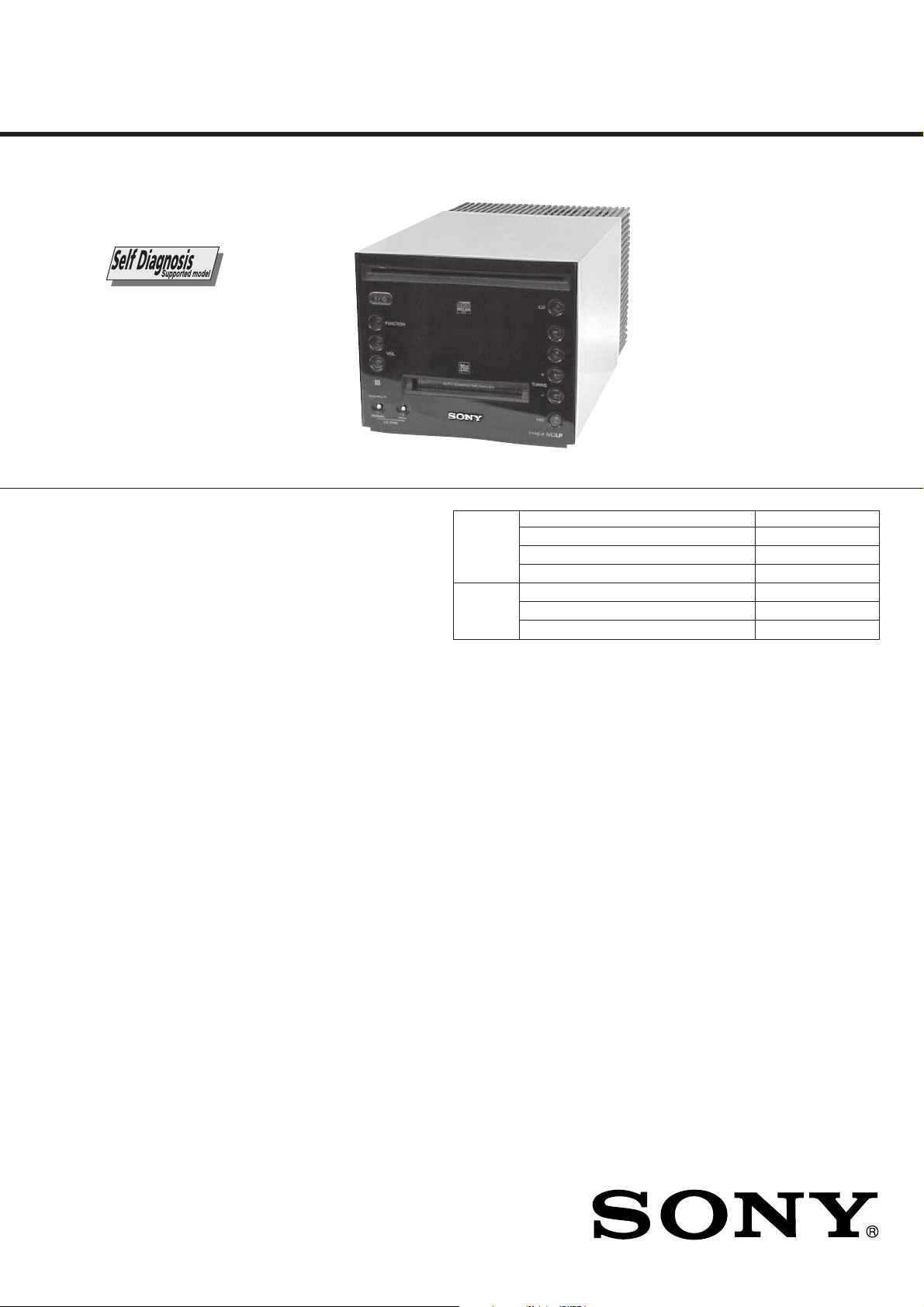
HCD-C5
SERVICE MANUAL
Ver 1.1 2001. 09
HCD-C5 is the Amplifier, CD player, MD
Deck and Tuner section in CMT-C5.
CD
Section
MD
Section
AEP Model
UK Model
E Model
Australian Model
Model Name Using Similar Mechanism New
CD Mechanism Type TN-CCD1001Z
Base Unit Name TT BASE ASSY
Optical Pick-up Name OPTIMA-720L1E
Model Name Using Similar Mechanism New
MD Mechanism Type MDM-7B4M
Optical Pick-up Name KMS-260E/Z-NP
Amplifier section
European model:
DIN power output (rated): 15 + 15 W
Continuous RMS power output (reference):
Music power output (reference):
Australian model:
The following measured at 230 V AC, 60 Hz
DIN power output (rated): 15 + 15 W
Continuous RMS power output (reference):
Other models:
The following measured at 220 V AC, 60 Hz
DIN power output (rated): 15 + 15 W
Continuous RMS power output (reference):
Inputs
TAPE IN (stereo minijack):
DIGITAL OPTICAL IN (Supported sampling
frequencies: 32 kHz, 44.1 kHz and 48 kHz)
Outputs
TAPE OUT (stereo minijack):
PHONES (stereo minijack):
(6 ohms at 1 kHz, DIN)
20 + 20 W
(6 ohms at 1 kHz, 10%
THD)
45 + 45 W
(6 ohms at 1 kHz, DIN)
20 + 20 W
(6 ohms at 1 kHz, 10%
THD)
(6 ohms at 1 kHz, DIN)
20 + 20 W
(6 ohms at 1 kHz, 10%
THD)
Sensitivity 250 mV,
impedance 47 kilohms
Sensitivity 250 mV,
impedance 1 kilohmes
Accepts headphones with
an impedance of 8 ohms
or more
SPECIFICATIONS
CD player section
System Compact disc and digital
Laser Semiconductor laser
Frequency response 2 Hz – 20 kHz
MD deck section
System MiniDisc digital audio
Laser Semiconductor laser
Sampling frequency 44.1 kHz
Frequency response 5 Hz – 20 kHz
Tuner section
FM stereo, FM/AM superheterodyne tuner
FM tuner section
Tuning range 87.5 – 108.0 MHz
Antenna FM wire antenna
Antenna terminals 75 ohm unbalanced
Intermediate frequency 10.7 MHz
AM tuner section
Tuning range
European model: 531 – 1,602 kHz
Other models: 530 – 1,710 kHz
Antenna AM loop antenna, external
Intermediate frequency 450 kHz
audio system
(λ = 780 nm)
Emission
duration: continuous
system
(λ=780 nm)
Emission duration:
continuous
(50-kHz step)
(with the tuning interval
set at 9 kHz)
(with the tuning interval
set at 10 kHz)
531 – 1,602 kHz
(with the tuning interval
set at 9 kHz)
antenna terminal
General
Power requirements
European model: 230 V AC, 50/60 Hz
Australian model: 230 V AC, 50/60 Hz
Other models: 220 V AC , 50/60 Hz
Power consumption
European model: See the nameplate
Other models: See the nameplate
Dimensions (w/h/d) Approx. 145 × 125 ×
Mass Approx. 4.5 kg
Supplied accessories Remote commander (1)
Design and specifications are subject to change
without notice.
0.5 W (at the power
saving mode)
273 mm incl. projecting
parts and controls
AM loop antenna (1)
FM wire antenna (1)
9-873-244-02
2001I1600-1
© 2001.9
MICRO HI-FI COMPONENT SYSTEM
Sony Corporation
Home Audio Company
Shinagawa Tec Service Manual Production Group
Page 2
HCD-C5
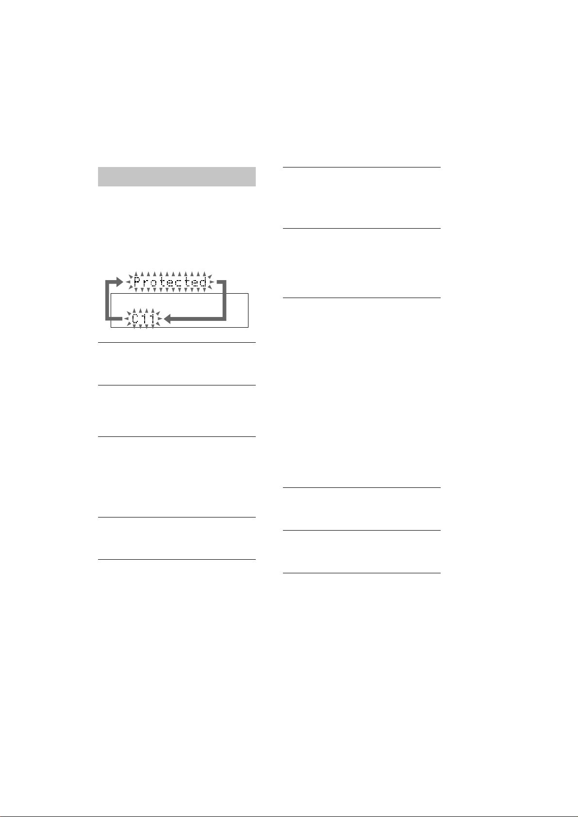
The self-diagnosis function consists of error codes for customers, which are displayed automatically when errors occur,
and error codes, which show the error history in the test mode during servicing. For details on how to view error codes
for the customer, refer to the following box in the instruction manual. For details on how to check error codes during
servicing, refer to the following “Procedure for using the Self-Diagnosis Function (Error History Display Mode)”.
SELF-DIAGNOSIS FUNCTION
Self-diagnosis display
This system has a Self-diagnosis display
function to let you know if there is a system
malfunction. The display shows a code made
up of 3 or 5 letters and a message alternately to
show you the problem. To solve the problem
refer to the following list. If any problem
persists, consult your nearest Sony dealer.
C11/Protected
The MD is protected against erasure.
cRemove the MD and slide the tab to close the
slot (see page 18).
C12/Cannot Copy
You tried to record a CD or MD with a format that
the system does not support, such as a CD-ROM.
cRemove the disc and turn off the system once,
then turn it on again.
C13/REC Error
Recording could not be performed properly.
cMove the system to a stable place, and start
recording over from the beginning.
The MD is dirty or scratched, or the MD does not
meet the standards.
cReplace the MD and start recording over from
the beginning.
C13/Read Error
The MD deck cannot read the disc information
properly.
cRemove the MD once, then load it again.
C14/Toc Error
The MD deck cannot read the disc information
properly.
cReplace the MD.
Erase all the recorded contents of the MD using
All Erase Function (see page 29).
C41/Cannot Copy
The sound source is a copy of a commercially
available music software, or you tried to record a
CD-R (Recordable CD).
cThe Serial Copy Management System prevents
making a digital copy (see page 48). You cannot
record a CD-R.
C71/Check OPT-IN
This appears momentarily because of the signal of
the digital broadcast during recording.
cThere is no affect on the recorded contents.
No component is connected to the DIGITAL
OPTICAL IN jack, or a digital component is not
connected properly.
cConnect a digital component to the DIGITAL
OPTICAL IN jack properly using a digital
connecting cable (not supplied, see page 43).
The connected digital component is not turned on.
cSee the operating instructions supplied with the
connected component and confirm whether the
component is turned on.
The digital connecting cable connected to the
DIGITAL OPTICAL IN jack is pulled out, or the
connected digital component is turned off during
digital recording.
cConnect the cable, or turn on the digital
component.
E0001/MEMORY NG
There is an error in the internal data that the system
needs in order to operate.
cConsult your nearest Sony dealer.
E0101/LASER NG
There is a problem with the optical pickup.
cThe optical pickup may have failed. Consult your
nearest Sony dealer.
2
Page 3

TABLE OF CONTENTS
SELF-DIAGNOSIS FUNCTION..................................... 2
1. SERVICING NOTES ............................................... 4
2. GENERAL ................................................................... 7
3. DISASSEMBLY ......................................................... 9
4. TEST MODE ............................................................... 24
5. ELECTRICAL ADJUSTMENTS
CD Section ...................................................................... 33
MD Section ..................................................................... 34
6. DIAGRAMS
6-1. NOTE FOR PRINTED WIRING BOARDS AND
SCHEMATIC DIAGRAMS ............................................ 45
– Wav e forms................................................................... 45
– Circuit Boards Location............................................... 45
6-2. Block Diagram – CD Servo Section –............................ 46
6-3. Block Diagram – MD Servo Section –........................... 47
6-4. Block Diagram – MAIN Section –................................. 48
6-5. Printed Wiring Boards – CD Section – .......................... 49
6-6. Schematic Diagram – CD Section –............................... 50
6-7. Printed Wiring Board – BD (MD) Board – .................... 51
6-8. Schematic Diagram – BD (MD) Board (1/2) –.............. 52
6-9. Schematic Diagram – BD (MD) Board (2/2) –.............. 53
6-10. Printed Wiring Board – MD DIGITAL Board – ............ 54
6-11. Schematic Diagram – MD DIGITAL Board – ............... 55
6-12. Printed Wiring Board – UCOM Board –........................ 56
6-13. Schematic Diagram – UCOM Board –........................... 57
6-14. Printed Wiring Boards – AUDIO Section –.................... 58
6-15. Schematic Diagram – AUDIO Section –........................ 59
6-16. Printed Wiring Board – PANEL Board – ....................... 60
6-17. Schematic Diagram – PANEL Board – .......................... 61
6-18. Printed Wiring Boards – POWER Section – .................. 62
6-19. Schematic Diagram – POWER Section – ...................... 63
6-20. IC Block Diagrams ......................................................... 64
6-21. IC Pin Function Description ........................................... 68
HCD-C5
7. EXPLODED VIEWS ................................................ 76
8. ELECTRICAL PARTS LIST .............................. 86
3
Page 4
HCD-C5
SECTION 1
SERVICING NOTE
NOTES ON HANDLING THE OPTICAL PICK-UP
BLOCK OR BASE UNIT
The laser diode in the optical pick-up block may suffer electrostatic
break-down because of the potential difference generated by the
charged electrostatic load, etc. on clothing and the human body.
During repair, pay attention to electrostatic break-down and also
use the procedure in the printed matter which is included in the
repair parts.
The flexible board is easily damaged and should be handled with
care.
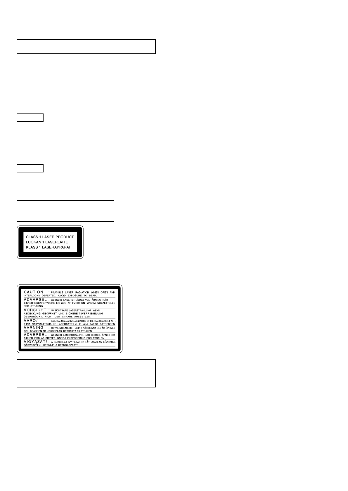
FOR CD
NOTES ON LASER DIODE EMISSION CHECK
The laser beam on this model is concentrated so as to be focused on
the disc reflective surface by the objective lens in the optical pickup block. Therefore, when checking the laser diode emission,
observe from more than 30 cm away from the objective lens.
FOR MD
NOTES ON LASER DIODE EMISSION CHECK
Never look into the laser diode emission from right above when
checking it for adjustment. It is feared that you will lose your sight.
Laser component in this product is capable
of emitting radiation exceeding the limit for
Class 1.
This appliance is classified as a CLASS 1 LASER product. The
CLASS 1 LASER PRODUCT MARKING is located on the bottom
exterior.
This caution
label is
located inside
the unit.
CAUTION
Use of controls or adjustments or performance of procedures
other than those specified herein may result in hazardous radiation
exposure.
Notes on chip component replacement
• Never reuse a disconnected chip component.
• Notice that the minus side of a tantalum capacitor may be
damaged by heat.
Flexible Circuit Board Repairing
• Keep the temperature of soldering iron around 270˚C
during repairing.
• Do not touch the soldering iron on the same conductor of the
circuit board (within 3 times).
• Be careful not to apply force on the conductor when soldering
or unsoldering.
4
SAFETY-RELATED COMPONENT WARNING!!
COMPONENTS IDENTIFIED BY MARK 0 OR DOTTED LINE WITH
MARK 0 ON THE SCHEMATIC DIAGRAMS AND IN THE PARTS
LIST ARE CRITICAL TO SAFE OPERATION. REPLACE THESE
COMPONENTS WITH SONY PARTS WHOSE PART NUMBERS
APPEAR AS SHOWN IN THIS MANUAL OR IN SUPPLEMENTS
PUBLISHED BY SONY.
Page 5
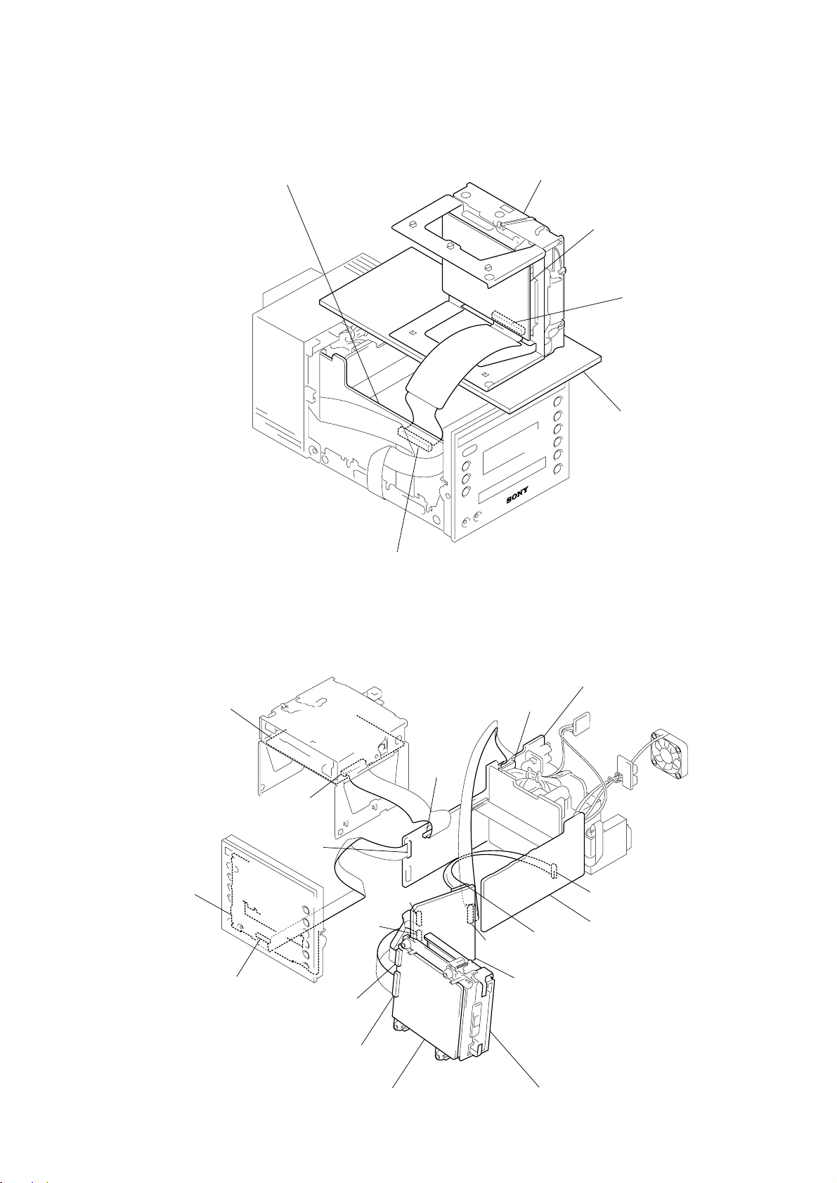
SERVICE POSITION OF THE CD MECHANISM DECK
D
UCOM BOARD
HCD-C5
CD MECHANISM DECK
(TN-CCD1001Z)
BD (CD) BOAR
CN101
STAND
CN204
SERVICE POSITION OF THE MD MECHANISM DECK
BD (CD) BOARD
CN204
CN101
CN201
PANEL BOARD
CN702
CN703
CN701
CN203
CN201
UCOM BOARD
CN102
AUDIO BOARD
CN601
CN103
CN102
BD (MD) BOARD
MD DIGITAL BOARD
MD MECHANISM (MDM-7B4M)
5
Page 6
HCD-C5
B
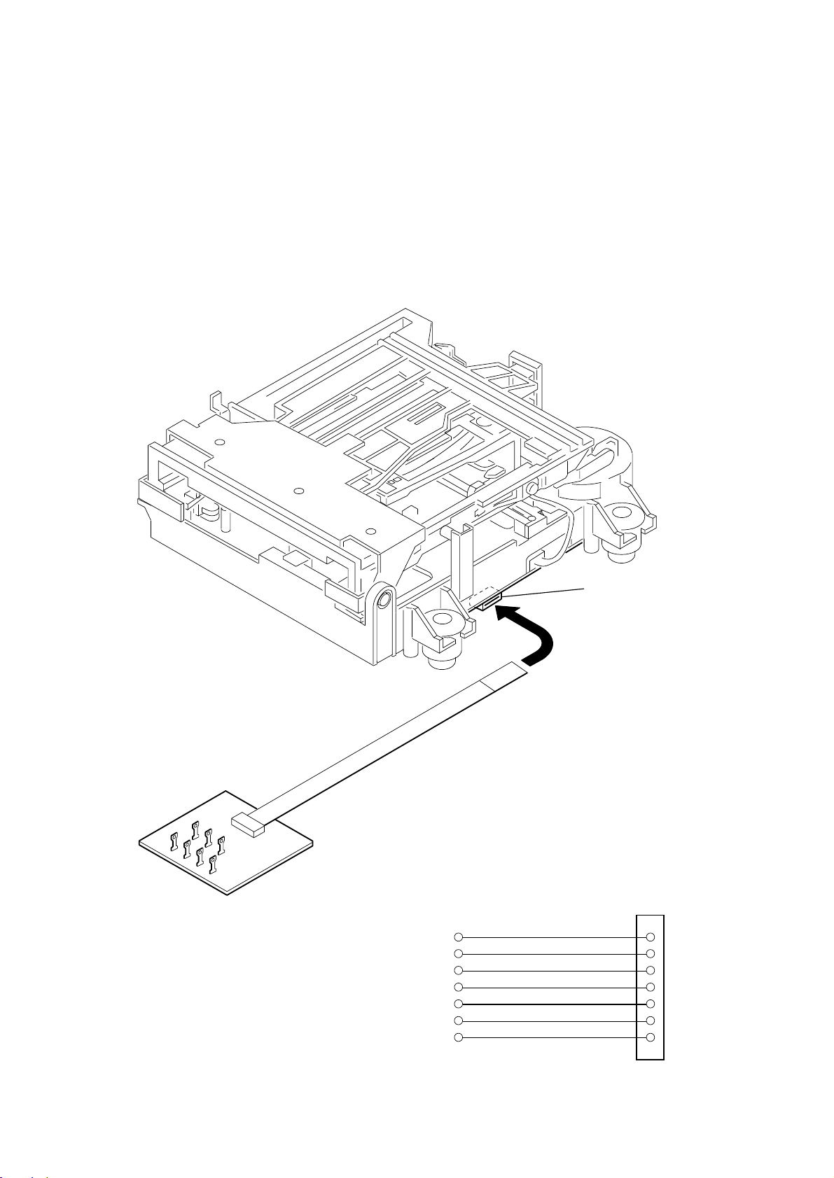
JIG FOR CHECKING BD (MD) BOARD WAVEFORM
The special jig (J-2501-196-A) is useful for checking the waveform of the BD (MD) board. The names of ter minals and the checking items
to be performed are shown as follows.
I+3V : For measuring IOP (Check the deterioration of the optical pick-up laser)
IOP : For measuring IOP (Check the deterioration of the optical pick-up laser)
GND : Ground
TE : Tracking error signal (Traverse adjustment)
FE : Focus error signal
VC : Reference level for checking the signal
RF : RF signal (Check jitter)
I+3V
GND
FE
RF
IOP
TE
VC
I+3V
IOP
GND
TE
FE
VC
RF
CN105
1
I+3V
IOP
GND
for 7
TE
FE
VC
RF
7
6
Page 7
SECTION 2
GENERAL
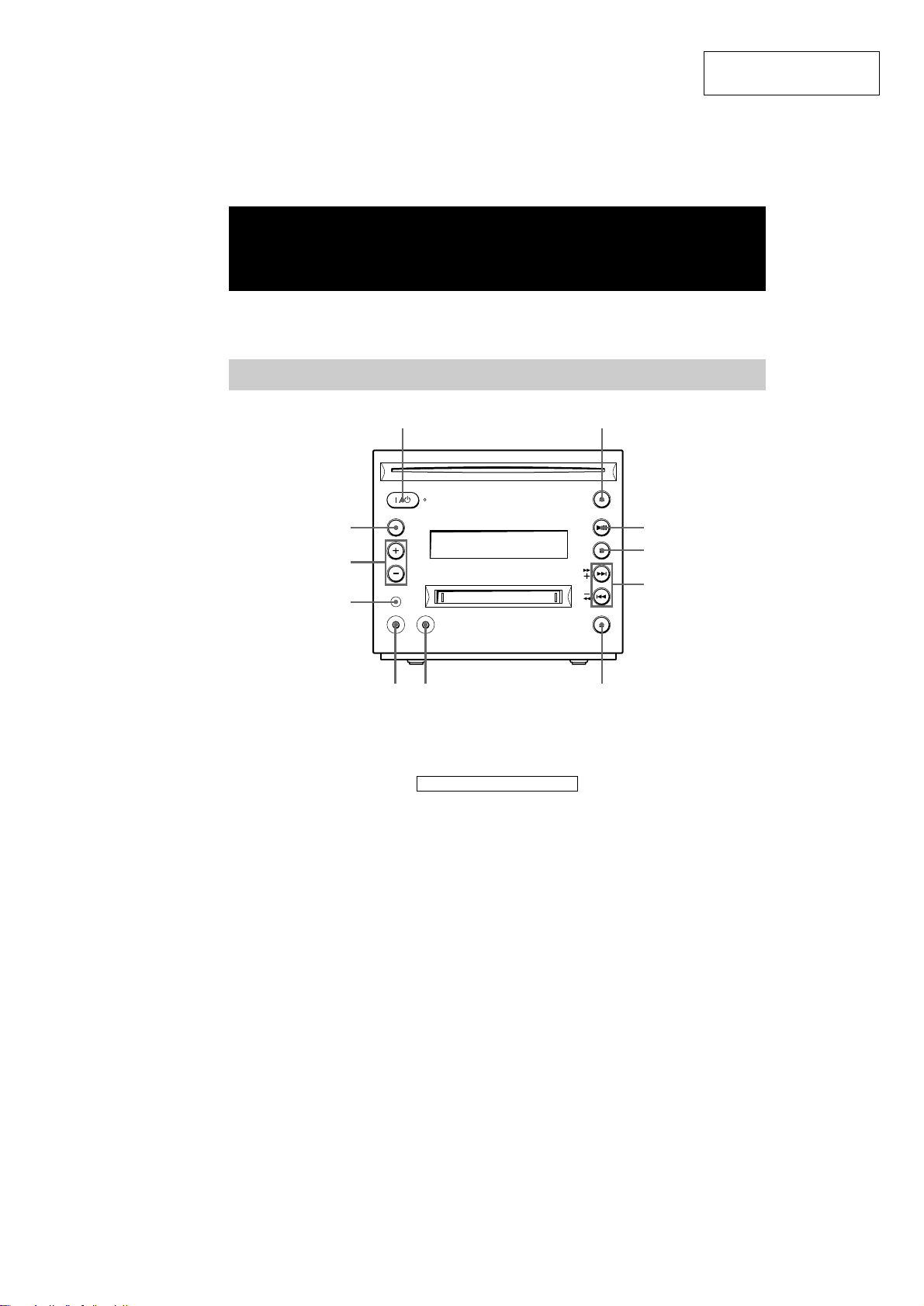
Parts Identification
The items are arranged in alphabetical order.
Refer to the pages indicated in parentheses () for details.
Main unit
12
HCD-C5
This section is extracted
from instruction manual.
qa
0
9
CD SYNC HIGH 7 (19, 51)
CD SYNC NORMAL 8 (19)
CD Z 2 (10, 51)
FUNCTION qa (9, 11, 13, 14, 16,
21–37, 44)
MD Z 6 (15, 18, 26)
REC/REC IT 8 (20, 21, 24, 26,
44, 51)
Remote sensor 9
TUNING +/– 5 (36, 37)
VOL +/– q; (40)
3
4
5
678
BUTTON DESCRIPTIONS
@/1 (power) 1 (7, 18, 26, 27, 37,
40, 42)
u 3 (9–11, 14–16, 19, 20, 25,
44)
x 4 (10, 11, 15, 16, 19–21, 26,
44)
. > 5 (10, 11, 13, 15, 16,
22–35)
m M 5 (10, 15, 30, 32)
4
7
Page 8
HCD-C5
Remote control
wk
wj
wh
wg
wf
wd
ws
wa
w;
Parts Identification
1 234
5
6
7
8
9
0
qa
qs
qd
qf
qg
qhqjqkql
CD x qh (10)
CD X ws (10)
CD N wd (9, 11, 20)
CLEAR 9 (11, 16, 28, 38)
CLOCK/TIMER SELECT 6
(41, 42)
CLOCK/TIMER SET 7 (8, 40,
41)
CURSOR T/t wh (8, 13, 28)
DBFB qf (39)
DISPLAY wk (8, 12, 17, 38)
ENTER/YES 8 (8, 11, 13, 14,
16, 21–36, 38, 40–42)
FM MODE qj (37)
FUNCTION w; (9, 11, 13, 14, 16,
19, 21–37, 44)
Letter/Number buttons wj (10,
13, 15, 16, 27, 28, 37)
Setting the time
1
Turn on the system.
2
Press CLOCK/TIMER SET on the
remote.
If you are setting the clock for the first time,
go to step 5.
3
Press – or + (. or >) on the
remote repeatedly until “CLOCK SET?”
appears in the display.
4
Press ENTER/YES on the remote.
The day indication flashes.
5
Press – or + (. or >) on the
remote repeatedly to set the day, and
then press ENTER/YES or CURSORt
on the remote.
The hour indication flashes.
MD x qs (15)
MD X wf (15)
MD N wg (14, 16, 19, 20, 25)
MENU/NO q; (13, 14, 22–26,
28–36)
NAME EDIT/SELECT 3 (13,
27, 28, 38)
PLAY MODE qk (9, 11, 14, 16,
26, 34, 35)
PRESET EQ qg (39)
REPEAT qj (10, 15)
SCROLL 5 (12, 14, 17, 28)
SLEEP 1 (39)
TIME 2 (8, 11, 12, 16, 17)
TUNER BAND wa (36, 37)
TUNING MODE qk (36, 37)
TUNING +/– ql (36, 37)
VOL +/– qd (40)
6
Press – or + (. or >) on the
remote to set the hour, and then press
ENTER/YES or CURSORt on the
remote.
The minute indication flashes.
7
Press – or + (. or >) on the
remote repeatedly to set the minute,
and then press ENTER/YES on the
remote.
If you made a mistake
Press TCURSOR or CURSORt on the
remote until the indication you wish to change
(day, hour, minute) flashes, and then change
the setting.
To reset the time
Start over from step 1.
BUTTON DESCRIPTIONS
@/1 (power) 4 (7, 18, 26, 27, 37,
40, 42)
. > qa (10, 11, 13–16, 22–
35, 40–42)
–/+ qa (8, 40, 42)
m M wh (10, 15, 30, 32, 42)
5
8
Page 9
• This set can be disassembled in the order shown below.
BOTTOM PLATE, CASE
(Page 10)
JACK BOARD, HP BOARD,
REAR COVER
(Page 18)
OVER WRITE HEAD
(Page 23)
SET
LOADING MOTOR (M703),
SPINDLE MOTOR (M701),
SLED MOTOR (M702)
(Page 22)
PANEL BOARD
(Page 10)
UCOM BOARD,
AMP POWER BOARD
(Page 19)
AUDIO BOARD,
POWER BOARD,
POWER TRANSFORMER
(T900) (1)
(Page 20)
CD MECHANISM DECK
(TN-CCD1001Z),
BD (CD) BOARD
(Page 11)
AUDIO BOARD,
POWER BOARD,
POWER TRANSFORMER
(T900) (2)
(Page 20)
MD MECHANISM DECK
(MDM-7B4M),
MD DIGITAL BOARD
(Page 21)
CONNECTOR BOARD
(Page 12)
FEED MOTOR ASSY (M903)
(Page 15)
REAR DAMPER BRACKET
(Page 15)
SW BOARD
(Page 14)
FRONT BRACKET SECTION,
LOADING MOTOR ASSY
(M902)
(Page 13)
SPINDLE MOTOR ASSY
(M904)
(Page 18)
BASE SECTION
(Page 17)
OPTICAL PICK-UP
(OPTIMA-720L1E),
SCREW GUIDE,
FEED SCREW ASSY, etc.
(Page 16)
OPTICAL PICK-UP
(OPTIMA-720L1E)
(Page 16)
HOLDER ASSY
(Page 21)
OP-SUB SECTION
(Page 23)
BD (MD) BOARD
(Page 22)
TUNER PACK,
D. C. FAN (M901)
(Page 19)
• The dotted square with arrow ( →) prompts you to move to the ne xt job when all of the w or ks within the dotted square ( ) are
completed.
HCD-C5
SECTION 3
DISASSEMBLY
9
Page 10
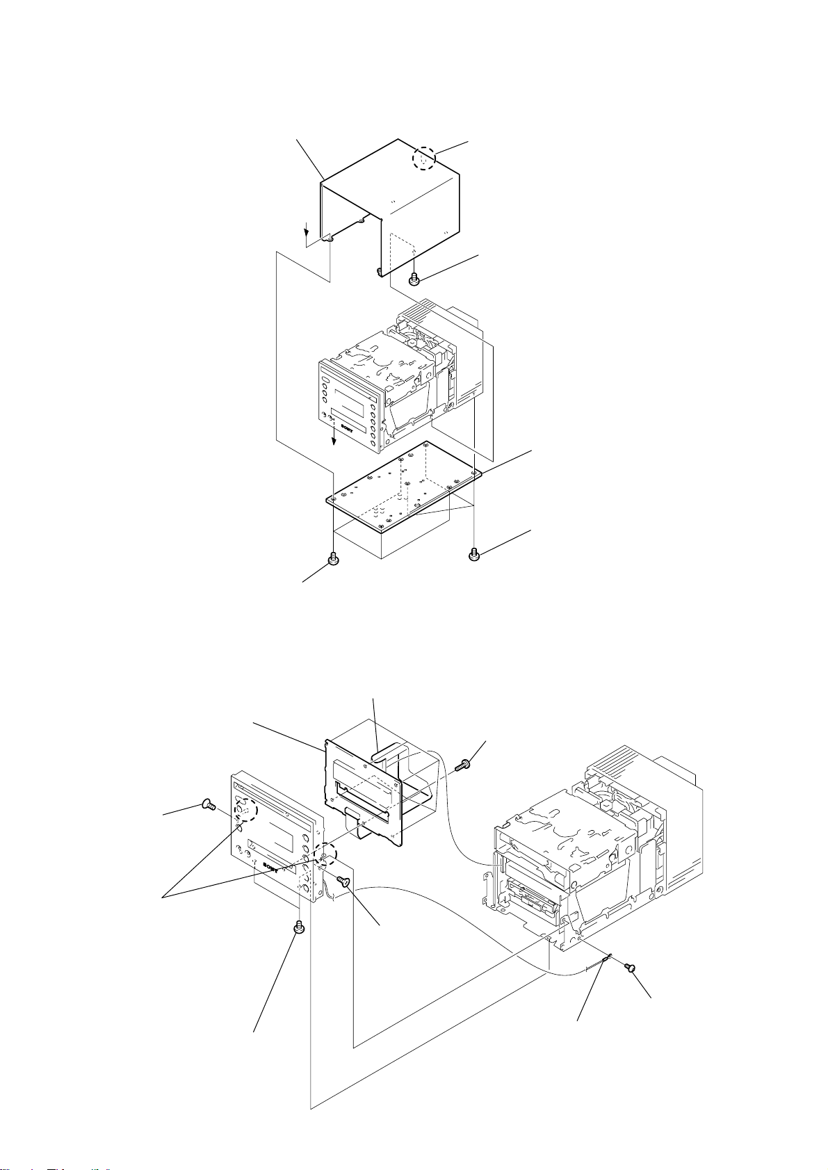
HCD-C5
)
Note: Follow the disassembly procedure in the numerical order given.
3-1. BOTTOM PLATE, CASE
6
case
A
A
5
claw
4
screw
(+BVTT 3 x 5)
3
2
(+BVTT 3 x 5)
bottom plate
three screws
3-2. PANEL BOARD
3
screw (+K 3 x 6)
8
two claws
9
PANEL board
1
four screws
(+BVTT 3 x 5)
6
wire (flat type)
(16 core) (CN201)
2
screw
(+K 3 x 6)
7
six screws
(+B 2 x 6)
10
1
two screws
(+BVTT 3 x 5)
5
ground wire
4
screw
(+BVTT 3 x 5
Page 11
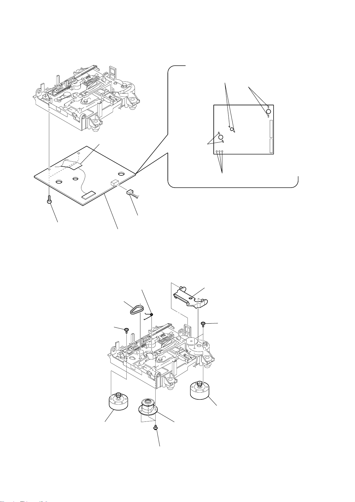
3-3. CD MECHANISM DECK (TN-CCD1001Z), BD (CD) BOARD
d
CN1
qd
CD mechanism deck
(TN-CCD1001Z)
7
board to board connector
9
two screws
(+BVTT 2.6 x 5)
CN103
qs
cushion (A)
q;
screw
(+BVTT 2 x 5)
qa
bracket (CD), foot (felt)
8
HCD-C5
BD (CD) boar
6
four screws
(+BVTT 3 x 5)
3
two screws
(+BVTT 3 x 5)
4
screw
(+BVTT 3 x 5)
5
wire (flat type) (29 core)
(CN204)
2
screw
(+BVTT 3 x 5)
1
two screws
(+BVTT 3 x 5)
11
Page 12
HCD-C5
d
3-4. CONNECTOR BOARD
6
(+P 2 x 2.5)
7
wire clamper
screw
5
FPC holder
8
CONNECTOR boar
1
Remove solderings
starting from the
left LOADING (+),
(–), red and black.
2
Remove solderings starting from the left
green, yellow, orange, red and brown.
3
Remove solderings starting from
the top left SPINDLE (+), (–), FD
MOTOR (+), (–) and the LIMIT
switch that has no polarity.
4
Remove the soldering.
12
Page 13
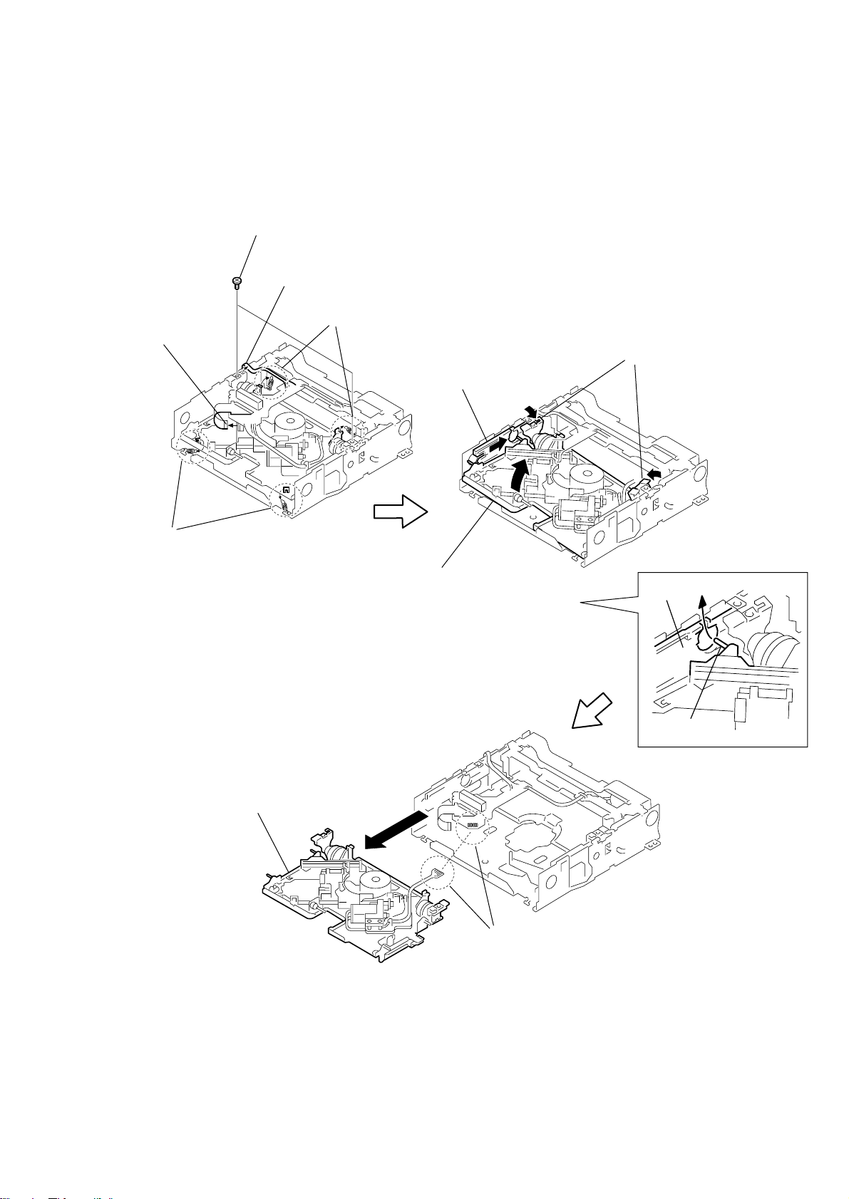
3-5. FRONT BRACKET SECTION, LOADING MOTOR ASSY (M902)
8
Remove it in the direction of
5
Remove the two
hang-up springs (FZ).
the arrow
when viewed from the rear of
the front bracket.
7
(M 2 x 4)
screw
A
from the left side
2
(M 2 x 2.5)
screw
HCD-C5
A
6
screw
(+P 2 x 3)
3
three claws
Note during re-assembling
When re-assembling, align the positions as shown.
1
FPC holder
4
Raise the
CONNECTOR board.
3
Move down the gear mount
bracket in the direction of the
arrow
B
.
B
1
wire clamper
3
loading motor assy (M902)
4
screw
(+P 2 x 3.0)
2
loading belt
2
Remove two solderings.
1
front backet section
13
Page 14
HCD-C5
3-6. SW BOARD
Release it from
2
the detents.
3
1
eleven claws
(BRN)
(RED)
(ORG)
(YEL)
(GRN)
2
switch (S3)
(Disc Existence, Chucking, Releasing detect)
1
Remove two solderings.
q;
SW board
5
Remove two solderings.
3
Remove two solderings.
14
9
Remove five solderings.
8
switch (S4)
(8cm Disc Eject End detect)
7
Remove two solderings.
4
switch (S2)
(12cm Disc/12cm
Disc Eject End detect)
6
switch (S1)
(Disc IN/8cm Disc detect)
Page 15
3-7. FEED MOTOR ASSY (M903)
t
two screws
1
(+P 2 x 10)
3
2
Remove the
soldering.
4
pulley gear
5
screw
(+P 2 x 3.0)
7
feed motor assy
(M903)
6
FD gear bracke
HCD-C5
3-8. REAR DAMPER BRACKET
2
screw
(+P 2 x 2.5)
4
screw
(+P 2 x 3)
1
wire clamper
3
two screws
(+P 2 x 3)
5
rear damper bracket
15
Page 16
HCD-C5
3-9. OPTICAL PICK-UP (OPTIMA-720L1E), SCREW GUIDE, FEED SCREW ASSY, etc.
4
screw
(+P 2 x 10)
6
optical pick-up (OPTIMA-720L1E),
screw guide,
feed screw assy, etc.
2
two screws
(+P 2 x 10)
1
pick-up flexible board
5
Slant the CONNECTOR board
in the direction of the arrow
A
.
A
3
feed motor assy (M903),
FD gear bracket, etc.
3-10. OPTICAL PICK-UP (OPTIMA-720L1E)
3
4
pulley M
1
screw guide
8
(OPTIMA-720L1E)
detent spring
optical pick-up
2
screw
(+P 1.7 x 6)
5
feed screw assy
7
pulley guide spring
16
6
screw
(+P 1.4 x 2)
Page 17
3-11. BASE SECTION
1
pick-up flexible
board
5
two screws
(+P2 x 5)
4
Remove solderings from
the damper pins.
2
springs (FZ) as shown.
Remove the two hang-up
1
Move the holder (L) in the
direction of the arrow
A
A
HCD-C5
2
Remove the two damper
.
pins toward inside.
3
Remove the two hang-up
springs (R) as shown.
2
base section
(
2
Remove the base block while the
mechanism is in the Loading IN state.)
B
3
Slant the base block in the
direction of the arrow
and remove the base
block from the main unit in
a manner that the lock pin
passes through the groove
of the holder (L) as shown.
B
holder (L)
lock pin
1
Remove solderings.
17
Page 18
HCD-C5
s
n
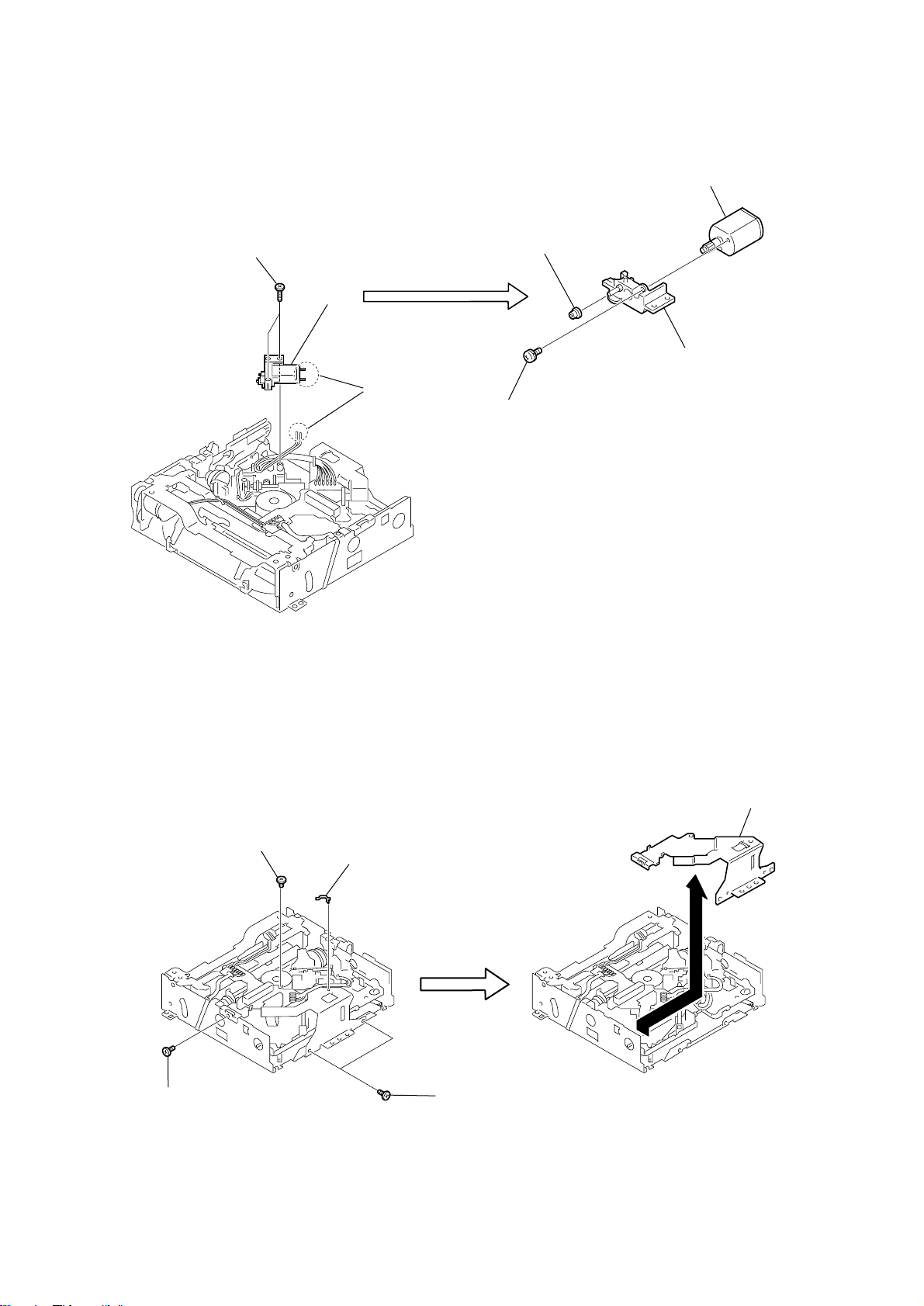
3-12. SPINDLE MOTOR ASSY (M904)
3
open to direction of the arrow
1
clip arm spring (L)
A
A
2
clip arm spring
4
two screws
(+P 1.7 x 2.2)
5
turn table
6
washer
8
spindle motor assy
(M904)
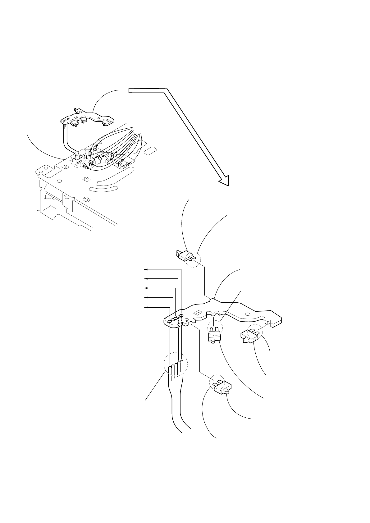
3-13. JACK BOARD, HP BOARD, REAR COVER
1
screw
(+BVTT 3 x 5)
2
four screws
(+BV 3 x 12)
3
three screws
(+BV 3 x 8)
7
5
connector
(CN109)
9
two nuts
(N4)
spindle motor
6
connector
(CN110)
4
screw
(+PTPWH 3 x 8)
2
connector
(CN107)
7
HP board
3
JACK board
1
two screws
(+BV 3 x 8)
8
two screw
(+B 4 x 16)
D.C.fa
(M901)
q;
rear cover
Note for re-installation-1
When installing the rear cover,
be careful that the three harnesses
coming from
2
Connector (CN107)”,
“
5
Connector (CN109)”,
“
6
Connector (CN110)”,
“
and the harness coming from the
DC fan (M901) must not contact the
heat sink (IC902) and the diode
(D981) and the heat sink (IC904).
18
POWER board
heat sink (IC902)
diode (D981)
Note for re-installation-2
When installing the rear cover, be careful that the three
harnesses coming from
2
Connector (CN107)”,
“
5
Connector (CN109)”,
“
6
Connector (CN110)”,
“
and the harness coming from the D.C. fan (M901) must not
be pinched by the rear cover, the UCOM board, power
transformer (T900) and tuner pack.
Page 19
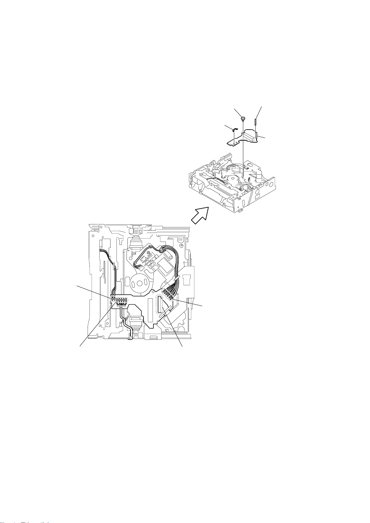
3-14. TUNER PACK, D. C. FAN (M901)
n
Note for re-installation
When installing the tuner pack, insert the three harnesses
connected to CN105 and connected to CN106 and
connected to CN108 of the AUDIO board, in between the
flat cable (11 core or 15 core) and the tuner pack in the
direction of the arrow so that the flat cable
(11 core or 15 core) must be inserted.
CN108
D.C.fan (M901)
CN105
CN106
2
wire (flat type)
(11 core or 15 core)
4
(CN105)
HCD-C5
connector
5
(M901)
1
screw
(+BV 3 x 8)
D.C. fa
wire (flat type)
AUDIO board
(11 core or 15 core)
tuner pack
3-15. UCOM BOARD, AMP POWER BOARD
8
AMP POWER baord
CN852
Note for re-installation
(routing the harnesses)
Be careful that the two harnesses between
CN995 and CN992 of the power transformer
(T900) and the POWER board must not
contact the heat sink (IC902) on the POWER
board and the flat cable (19 core) that
is inserted to CN203 on the UCOM board.
heat sink (IC902)
CN995
POWER baord
wire (flat type)
(19 core)
CN203
AMP POWER
board
3
(After slanted toward outside,
remove it straight up toward outside.)
7
board to board
connector
2
wire (flat type)
(19 core) (CN203)
tuner pack
CN206
CN901
3
connector
(CN851)
1
wire (flat type)
(19 core) (CN101)
9
CN205
A
5
board to board
connector
A
4
(+BVTT 3 x 5)
6
wire (flat type)
(16 core) (CN201)
UCOM board
two screws
UCOM board
CN851
CN992 power transformer (T900)
19
Page 20
HCD-C5
r
3-16. AUDIO BOARD, POWER BOARD, POWER TRANSFORMER (T900) (1)
6
AUDIO board, POWER boad,
power transformer (T900 ), etc.
1
two screws
(+BVTT 3 x 5)
5
connector
(CN102)
2
(+BV 3 x 8)
3
four screws
4
two screws
(+BVTT 3 x 5)
(+BVTT 3 x 5)
3-17. AUDIO BOARD, POWER BOARD, POWER TRANSFORMER (T900) (2)
qs
insulated plates (POWER)
qa
nylon rivet (DIA 3.5)
q;
D.C.fan (M901)
qg
9
connector (CN105)
qh
AUDIO board
POWER board
qf
board to board
connector
screw
qd
insulated plates (POWER) 2
2
connector (CN992)
3
clamp
1
connector (CN995)
20
CN103
7
wire (flat type) (11 core)
(from tuner pack)
CN902
8
tuner pack
5
connector (CN991)
4
power transforme
(T900)
6
power cord
Page 21
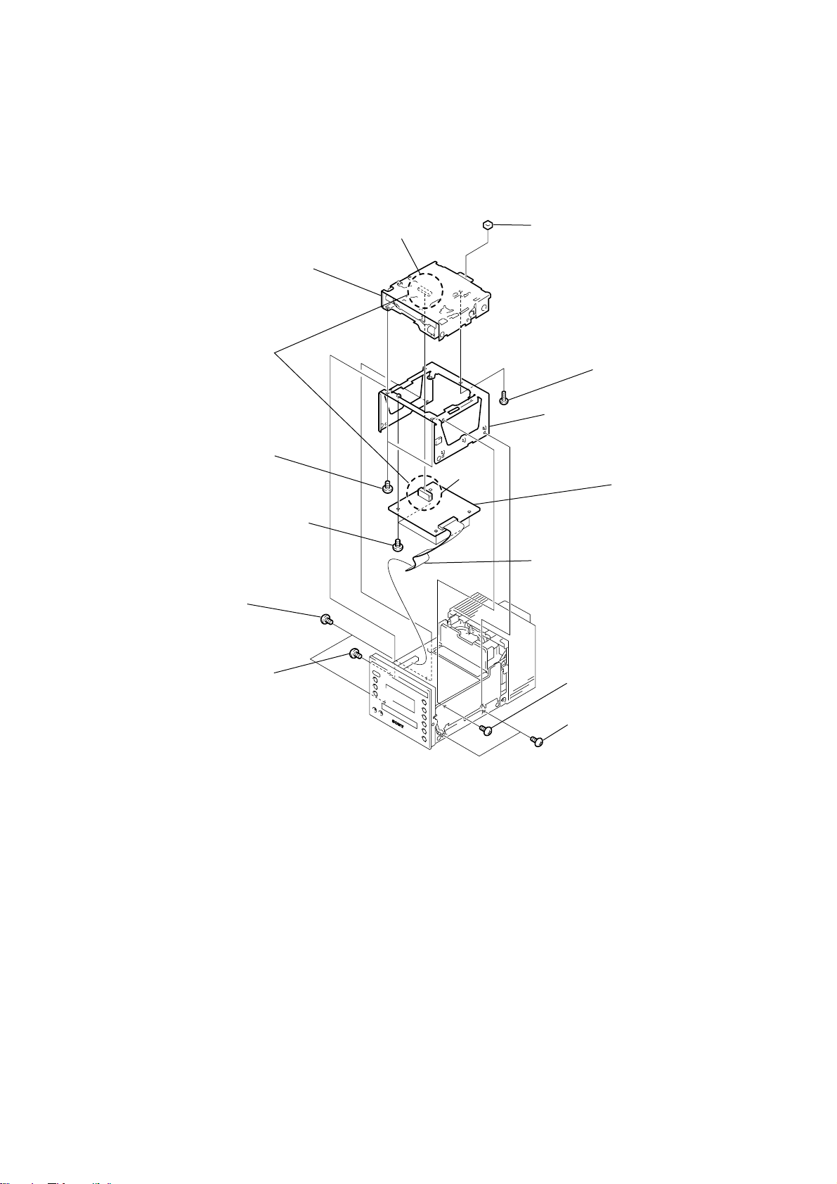
3-18. MD MECHANISM DECK (MDM-7B4M), MD DIGITAL BOARD
k
7
two screws
(+BVTT 3 x 5)
4
shield (MD2)
2
two screws
(+BVTT 3 x 5)
3
ground
wire
8
MD DIGITAL board
1
four screws
(+BVTT 3 x 5)
9
shield (MD1)
HCD-C5
q;
four screws, step
Slant the shield (MD1), shield (MD2) and
the MD DIGITAL board in the direction of
the arrow and remove the two
screws (+BVTT 3 x 5).
2
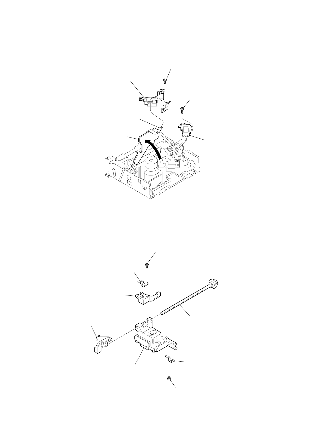
3-19. HOLDER ASSY
1
tension spring (holder)
qa
qs
screw
(+BTN 1.7 x 3)
3
holder assy
four insulators
qd
ground wire
5
wire (flat type)
(17 core) (CN703)
6
wire (flat type)
(27 core) (CN702)
qf
MD mechanism deck
(MDM-7B4M)
2
hoo
21
Page 22
HCD-C5
)
)
3-20. BD (MD) BOARD
2
Remove two solderings.
(spindle)
1
Remove two solderings.
(sled)
M702
M701
6
(CN101)
5
two screws
(+BP TRI 2 x 6 CZN)
flexible board
8
BD (MD) board
7
connector (CN104)
3
Remove two
solderings.
(loading)
M703
S102
4
Remove three solderings.
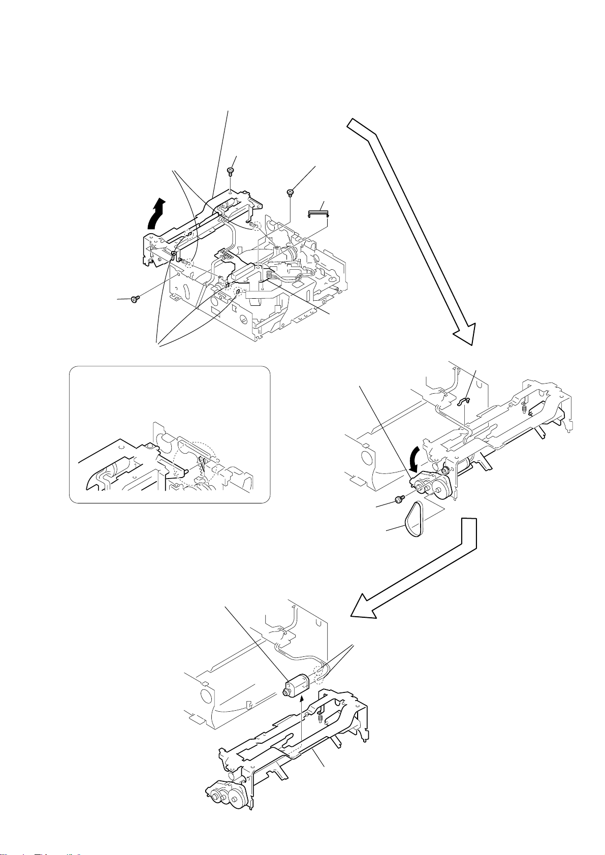
3-21. LOADING MOTOR (M703), SPINDLE MOTOR (M701), SLED MOTOR (M702)
1
3
torsion spring (spindle)
2
belt (loading)
lever (head)
22
4
two screws
(+PWH 1.7 x 3.5)
5
loading motor (M703)
7
spindle motor (M701)
6
three tapping screws (M1.7)
8
two screws
(+PWH 1.7 x 3.5
9
sled motor (M702
Page 23
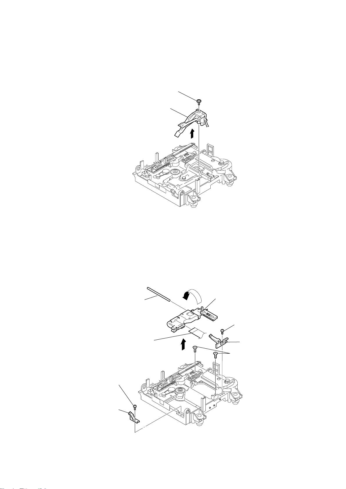
3-22. OVER WRITE HEAD
)
2
over write hrad
(HR901)
1
screw (+P 1.7 x 6)
HCD-C5
3-23. OP-SUB SECTION
1
screw
(+BP TRI 2 x 6 CZN)
2
base (BU-D)
8
main shaft
9
flexible board
6
7
q;
optical pick-up (for MD)
3
screw
(+BP TRI 2 x 6 CZN
4
base (BU-A)
5
screw (+KTP 2 x 6)
23
Page 24
HCD-C5
SECTION 4
TEST MODE
[Factory Preset Mode]
∗ This mode clears all data including preset data stored in the
RAM to initial conditions. Excute this mode when returning
the set to the customer.
Procedure:
1. Press the ?/1 button to turn the power on.
2. Press the FUNCTION z button to set the CD function.
(except the TUNER function)
3. Press three buttons VOL + , CD Z and MD Z
simultaneously.
4. The message “COLD RESET” blinks and the present contents
are reset to the default values.
[Version and Destination Display Mode]
∗ The version or destination is displayed.
Procedure:
1. Press the ?/1 button to turn the power on.
2. To enter the test mode, press the three buttons VOL + , x
and MD Z simultaneously.
3. The model and destination are displayed.
4. Press the REC/REC IT/NORMAL and u buttons simul-
taneously.
5. The version is displayed as “STR/CD V . ”.
6. Press the REC/REC IT/NORMAL and u buttons simul-
taneously.
7. The version is displayed as “MD V . ”.
8. Press the REC/REC IT/NORMAL and u buttons simul-
taneously, then the mode returns to step 3.
9. To exit from this mode, press the ?/1 button to turn the
power off.
[FL Tube Test Mode]
∗ All fluorecent segments and LEDs are tested.
Procedure:
1. Press the ?/1 button to turn the power on.
2. To enter the test mode, press three buttons VOL + , x and
./m TUNING - simultaneously.
3. All segments and LEDs are turned on.
4. Press the REC/REC IT/NORMAL and u buttons simul-
taneously.
5. All segments are turned off (All LEDs still lit).
6. Press the REC/REC IT/NORMAL and u buttons simul-
taneously.
7. Almost half segments are turned on. (PATTERN 1)
[Key Test Mode]
∗ Keyboard check.
Procedure:
1. Press the ?/1 button to turn the power on.
2. To enter the test mode, press three buttons VOL + , x and
>/M TUNING + simultaneously.
3. In the key test mode, the fluorecent indicator displays
“KEY00”.
4. Each time a button is pressed, “KEY ” value increases.
However, once a button is pressed, it is no longer taken into
account.
5. To exit from this mode, press three buttons simultaneously as
step 2 , or disconnect the power cord.
[Amp Test Mode]
Procedure:
1. Press the ?/1 button to turn the power on.
2. Press three buttons VOL - , CD Z and MD Z simulta-
neously.
3. Press two buttons REC/REC IT/NORMAL and x simulta-
neously.
4. The message “7 [TESTMIN]” is displayed for a few seconds.
5. Press two buttons REC/REC IT/NORMAL and x simulta-
neously again.
6. Each time two buttons are depressed, the display changes as
“8 [TESTMID]” , “9 [TESTMAX]”, and “10 [TESTSUR]” .
7. Press the VOL + button, the display changes “VOLUME 21”
to “VOLUME MAX”.
8. Press the VOL - button, the display changes “VOLUME 21”
to “VOLUME MIN”.
9. To exit from this mode, press the ?/1 button to turn the
power off and cold reset is executed.
[CD Test Mode]
∗ The CD system versions are displayed.
Procedure:
1. Press the ?/1 button to turn the power on.
2. Press the FUNCTION z button to set the CD function.
3. Press three buttons of VOL + , x and CD SYNC HIGH
simultaneusly.
4. The message “dut CD VER” is displayed.
5. Press the CD Z button and the version “CD
played.
6. Press the >/M TUNING + button and “CDSYS ”
is displayed.
7. Each time the >/M TUNING + button is depressed ,
the display changes as “CDMA S”, “CDBD O”, “CDCD M”.
8. By depressing the ./m TUNING - button the versions
are displayed in reverse.
9. To exit this mode, press the ?/1 button to turn the power off .
. ” is dis-
8. Press the REC/REC IT/NORMAL and u buttons simul-
taneously.
9. The segments which are turned on in step 7 are turned off,
then remaining segments are turned on. (PATTERN 2)
10. Press the REC/REC IT/NORMAL and u buttons simul-
taneously, the mode returms to step 3 and all segments are
turned on.
11. To exit from this mode, press the ?/1 button to turn the
power off.
24
Page 25
HCD-C5
[CD Aging Mode]
Procedure:
1. Press the ?/1 button to turn the power on.
2. Press the FUNCTION z button to set the CD function, and
insert a disc.
3. Press three buttons of VOL - , CD Z and
>/M TUNING + simultaneusly.
4. The message “Eject” is displayed, a disc is ejected and inserted again automatically.
5. The sequence during the CD aging mode is following as below.
CD aging mode sequence:
CD disc eject
CD disc in
TOC reading
Playback the first track
Playback the last track
Display the number of aging
MD SECITON
Note 1: About “R”
As this unit has only a few buttons, some operations require
the use of remote commander (RM-SC5BEN/provided with
unit: 1-476-649-21) buttons. These operations are indicated
as “R” in this manual.
Example: MENU/NO “R” ...Press the MENU/NO b utton of
the remote commander.
Note 2: Incorrect operations may be performed if the MD test mode
is not entered properly.
In this case, press the ?/1 button to turn the po wer of f, and
retry to enter the MD test mode.
1. PRECAUTIONS FOR USE OF TEST MODE
• As operations related to loading will be performed regardless of
the test mode operations being performed, be sure to check that
the disc is stopped before setting and removing it.
Even if the MD Z button is pressed while the disc is rotating
during continuous playback, continuous recording, etc., the disc
will not stop rotating.
Therefore, it will be ejected while rotating.
Be sure to press the MD Z button after pressing the
MENU/NO “R” button and the rotation of disc is stopped.
6. To exit this mode , press the ?/1 button to turn the power
off.
[CD/MD Aging Mode]
∗ Aging of CD and MD is performed at the same time.
Procedure:
1. Press the ?/1 button to turn the power on.
2. Press the FUNCTION z button to set the CD function.
3. Insert a disc (CD) and a recordable disc (MD).
4. Press three buttons of VOL + , u and MD Z
simultaneusly.
5. The message “Eject” is displayed and aging started.
6. The sequence of CD aging is same as the CD aging mode,
however the MD aging is r epetition of changing the track after
a few seconds recording.
7. The number of aging is displayed in hexadecimal. For example,
AGING00000011 means the 17th rouine of aging.
8. To exit this mode, press the ?/1 b utton to turn the power of f,
or press three buttons of VOL + , CD Z and MD Z simul-
taneously and cold reset is executed.
1-1. Recording laser emission mode and operating
buttons
• Continuous recording mode (CREC 1MODE)
• Laser power check mode (LDPWR CHECK)
• Laser power adjustment mode (LDPWR ADJUST)
• Comparison with initial Iop value written in nonv olatile memory
(Iop Compare)
• Write current Iop value in read nonvolatile memory using microprocessor (Iop NV Save)
• Traverse (MO) check (EF MO CHECK)
• Traverse (MO) adjustment (EF MO ADJUST)
• When pressing the REC/REC IT button.
2. SETTING THE TEST MODE
The following is the method of entering the test mode.
Procedure: 1. Press the ?/1 button to turn the power on.
2. Press the FUNCTION z button to set the MD
function.
3. Press three buttons of VOL - , x , and
CD SYNC HIGH (MD) simulta neously.
When the test mode is set, “[Check]” will be
displayed. Pressing the
. “R” or > “R” button between the
following three groups; ··· Tt [Check] Tt
[Service] Tt [Develop] Tt ···.
Note: Do not use the test mode in the [Develop] group.
If used, the unit may not operate normally.
If the [Develop] group is set accidentally, press the
MENU/NO “R” button immediately to exit the [Develop] group.
3. RELEASING THE TEST MODE
Procedure 1: Press the REPEAT “R” button to display “Initial-
ize”, then release the MD test mode.
Procedure 2: Press two button of VOL - and MD Z to display
“Intialize”, then release the MD test mode.
25
Page 26
HCD-C5
4. BASIC OPERATIONS OF THE TEST MODE
All operations are performed using the . “R” , > “R” , ENTER/YES “R” and MENU/NO “R” .
The functions of these buttons are as follows.
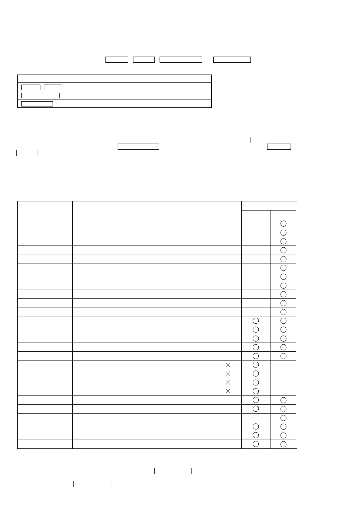
Function name Function
. “R” , > “R” buttons Changes parameters and modes
ENTER/YES “R” button Proceeds onto the next step. Finalizes input
MENU/NO “R” button Returns to previous step. Stops operations
5. SELECTING THE TEST MODE
There are 26 types of test modes as shown below. The groups can be switched by pressing the . “R” or > “R” button.
After selecting the group to be used, press the ENTER/YES “R” button. After setting a certain group, pressing the . “R” or
> “R” button switches modes shown belo w.
Refer to “Group” in the table for details can be selected.
All items used for servicing can be treated using group [Service]. So be carefully not to enter other groups by mistake.
Note: Do not use the test mode in the [Develop] group.
If used, the unit may not operate normally.
If the [Develop] group is set accidentally, press the MENU/NO “R” button immediately to exit the [Develop] group.
Display
AUTO CHECK
Err Display
TEMP ADJUST
LDPWR ADJUST
Iop Write
Iop NV Save
EF MO ADJUST
EF CD ADJUST
FBIAS ADJUST
AG Set (MO)
AG Set (CD)
TEMP CHECK
LDPWR CHECK
EF MO CHECK
EF CD CHECK
FBIAS CHECK
ScurveCHECK
VERIFYMODE
DETRK CHECK
0920 CHECK
Iop Read
Iop Compare
ADJ CLEAR
INFORMATION
CPLAY1MODE
CREC 1MODE
No.
Automatic self-diagnosis
C01
Error history display, clear
C02
Temperature compensation offset adjustment
C03
Laser power adjustment
C04
Iop data writing
C05
Writes current Iop value in read nonv olatile memory using microprocessor
C06
Traverse (MO) adjustment
C07
Traverse (CD) adjustment
C08
Focus bias adjustment
C09
Auto gain output level adjustment (MO)
C10
Auto gain output level adjustment (CD)
C11
Temperature compensation offset check
C12
Laser power check
C13
Traverse (MO) check
C14
Traverse (CD) check
C15
Focus bias check
C16
S-curve check
C17
Nonvolatile memory check
C18
Detrack check
C19
Most circumference check
C25
Iop data display
C26
Comparison with initial Iop value written in nonvolatile memory
C27
Initialization of nonvolatile memory for adjustment values
C28
Display of microprocessor version, etc.
C31
Continuous playback mode
C34
Continuous recording mode
C35
Details
Mark
Group
Check Service
• For details of each adjustment mode, refer to “5. Electrical Adjustments”.
For details of “Err Display”, refer to “Self-Diagnosis Function” on page 2.
• If a different mode has been selected by mistake, press the MENU/NO “R” button to release that mode.
• Modes with (×) in the Mark column are not used for servicing and therefore are not described in detail. If these modes are set
accidentally, press the MENU/NO “R” button to release the mode immediately.
26
Page 27
HCD-C5
“CREC 1MID” t “CREC 1OUT” t “CREC 1IN”
5-1. Operating the Continuous Playback Mode
1. Entering the continuous playback mode
(1) Set the disc in the unit. (Whichev er recordable discs or discs
for playback only are available)
(2) Press the . “R” or > “R” button to display
“CPLAY1MODE” (C34).
(3) Press the ENTER/YES “R” button to change the display
to “CPLAY1MID”.
(4) When access completes, the display changes to “C =
AD = )”.
Note: The numbers “ ” displayed show you error rates and ADER.
2. Changing the parts to be played back
(1) Press the ENTER/YES “R” button during continuous play-
back to change the display as below.
“CPLAY1MID” t “CPLAY1OUT” t “CPLAY1IN”
When pressed another time, the parts to be played back can
be moved.
(2) When access completes, the display changes to “C =
AD = )”.
Note: The numbers “ ” displayed show you error rates and ADER.
3. Ending the continuous playback mode
(1) Press the MENU/NO “R” button. The display will change
to “CPLAY1MODE” (C34).
(2) Press the MD Z button and take out the disc.
Note: The playback start addresses for IN, MID, and OUT
are as follows.
IN : 40h cluster
MID : 300h cluster
OUT : 700h cluster
5-2. Operating the Continuous Recording Mode (Use
only when performing self-recording/palyback
check)
1. Enter ing the continuous recording mode
(1) Set a recordable disc in the unit.
(2) Press the . “R” or > “R” button to display “CREC
1MODE” (C35).
(3) Press the ENTER/YES “R” b utton to change the display to
“CREC 1MID”.
(4) When access completes, the display changes to “CREC 1(
)” and “ REC ” is displayed.
Note: The numbers “ ” displa yed shows you the recording posi-
REC
tion addresses.
2. Changing the parts to be recorded
(1) When the ENTER/YES “R” button is pressed during con-
tinuous recording, the display changes as below.
When pressed another time, the parts to be recorded can be
changed. “ REC ” goes off.
REC
(2) When access completes, the display changes to “CREC 1(
)” and “ REC ” is displayed.
Note: The numbers “ ” displayed shows you the recording posi-
tion addresses.
REC
3. Ending the continuous recording mode
(1) Press the MENU/NO “R” button. The display changes to
“CREC 1MODE” (C35) and “ REC ” goes off.
REC
(2) Press the MD Z button and take out the disc.
Note 1: The recording start addresses for IN, MID, and OUT are
as follows.
IN : 40h cluster
MID : 300h cluster
OUT : 700h cluster
Note 2: The MENU/NO “R” button can be used to stop recording
Note 3: Do not perform continuous recording for long periods of
Note 4: During continuous recording, be careful not to apply vi-
anytime.
time above 5 minutes.
bration.
27
Page 28
HCD-C5
6. FUNCTIONS OF OTHER BUTTONS
Function
u
x
M “R”
m “R”
x + >/M TUNING +
VOL - + CD Z
MD Z
REPEAT “R”
Sets continuous playback when this is pressed in the STOP state. When this is pressed during continuous playback, playback position moves.
Stops continuous playback and continuous recording
The sled moves to the outer circumference only when this is pressed
The sled moves to the inner circumference only when this is pressed
Switches the spindle servo mode (CLV S y CLV A)
Switches the displayed contents each time the button is pressed
Ejects the disc
Releases the test mode
7. AUTOMATIC SELF-DIAGNOSIS FUNCTION
This test mode performs CREC and CPLAY automatically for mainly checking the characteristics of the optical pick-up.
To perform this test mode, the laser power must first be checked.
Perform AUTO CHECK after the laser power check and Iop Compare.
Procedure:
1. Press the . “R” or > “R” button to display “AUTO CHECK” (C01).
2. Press the
performed. In this case, perform the laser power check and Iop Compare, and then repeat from enter the MD test mode.
3. If a disc is in the mechanical deck, it will be ejected forcibly.
“DISC IN” will be displayed in this case. Load a test disc (MDW-74/GA-1) which can be recorded.
4. If a disc is loaded at step 3, the check will start automatically.
5. When “XX CHECK” is displayed, the item corresponding to XX will be performed.
When “060 CHECK” completes, the disc loaded at step 3 will be ejected. “DISC IN” will be displayed. Load the check disc
(TDYS-1).
6. When the disc is loaded in step 5, the check will automatically be resumed from “07 CHECK”.
7. After completing to test item 12 (“oC CHECK”), check OK or NG will be displayed. If all items are OK, “CHK ALL OK” will
be displayed. If any item is NG, it will be displayed as “NG:xxxx”.
ENTER/YES “R” button. If “LDPWR ” is displayed, it means that the laser power check has not been
Contents
When “CHK ALL OK” is displayed, it means that the optical pick-up is normal. Check the operations of other parts (spindle
motor, sled motor, etc.).
When displayed as “NG:xxxx”, it means that the optical pick-up is faulty. In this case, replace the optical pick-up.
8. INFORMATION
Display the software version.
Procedure:
1. Press the . “R” or > “R” button to display “INFORMATION” (C31).
2. Press the ENTER/YES “R” button.
3. The software version will be displayed.
4. Press the MENU/NO “R” button to end this mode.
28
Page 29

HCD-C5
IOP DATA RECORDING AND DISPLAY WHEN OPTICAL PICK-UP AND NON-VOLATILE MEMORY (IC195
OF BD (MD) BOARD) ARE REPLACED
The IOP value labeled on the optical pick-up can be recorded in
the non-volatile memory . By recording the v alue, it will eliminate
the need to look at the value on the label of the optical pick-up.
When replacing the optical pick-up or non-volatile memory (IC195
of BD (MD) board), record the IOP value on the optical pick-up
according to the following procedure.
Record Procedure:
1. Press the ?/1 button to turn the power on.
2. Press the FUNCTION z button to set the MD function.
3. Press three buttons of VOL - , x and CD SYNC HIGH ,
simultaneously to enter the MD test mode and display
“[Check]”.
4. Press the . “R” or > “R” button to display
“[Service]”.
5. Press the ENTER/YES “R” button to display “AUTO
CHECK”, and press the > “R” button to display “Iop
Write”.
6. Press the ENTER/YES “R” button.
7. The display becomes “Ref= @@@.@” (@ is an arbitrary number) and the numbers which can be changed will blink.
8. Input the IOP value written on the optical pick-up.
To select the number : Press the
. “R” or > “R” button.
To select the digit : Press two buttons of VOL - and
CD Z simultaneously.
9. When the ENTER/YES “R” button is pressed, the display
becomes “Measu=@@@.@” (@ is an arbitrary number).
10. As the adjustment results are recorded for the step 9 value.
Leave it as it is and press the ENTER/YES “R” button.
11. “Complete!” will be displayed momentarily. The value will
be recorded in the non-volatile memory and the display will
become “Iop Write”.
12. Press the REPEAT “R” button, or press two buttons of
VOL - and MD Z simultaneously. to complete. “Initializ e”
will be displayed and release the MD test mode.
WHEN MEMORY NG IS DISPLAYED
If the nonvolatile memory data is abnormal, “E001 MEMOR Y NG”
will be displayed so that the MD deck does not continue operations. In this case, set the test mode promptly and perform the
following procedure.
Procedure:
1. Enter the MD test mode.
2. Normally a message for selecting the test mode will be displayed.
However if the nonvolatile memory is abnormal, the following
will be displayed “INIT EEP?”.
3. Press the x and MD Z buttons simultaneously.
4. Press the . “R” or > “R” button to display “MDM-7B4M”.
5. Press the ENTER/YES “R” button. If the nonvolatile memory is
successfully overwritten, the normal MD test mode will be set
and a message to select the MD test mode will be displayed.
Display Precedure:
1. Press the ?/1 button to turn the power on.
2. Press the FUNCTION z button to set the MD function.
3. Press three buttons of VOL - , x , and CD SYNC HIGH
simultaneously to enter the MD test mode and display
“[Check]”.
4. Press the . “R” or > “R” button to display “[Service]”.
5. Press the ENTER/YES “R” button to display “AUTO
CHECK”, and press the > “R” button to display “Iop Read”.
6. Press the ENTER/YES “R” button.
7. “@@.@/##.#” is displayed and the recorded contents are displayed.
@@.@ : Indicates the Iop value labeled on the pick-up.
##.# : Indicates the Iop value after adjustment.
8. Press the REPEAT “R” button to complete. “Initialize” will
be displayed and release the MD test mode.
29
Page 30
HCD-C5
CHECKS PRIOR TO PARTS REPLACEMENT AND ADJUSTMENTS IN MD
Before performing repairs, perform the following checks to determine the faulty locations up to a certain extent.
Details of the procedures are described in “5 Electrical Adjustments”.
Criteria for Determination
(Unsatisfactory if specified value is not satisfied)
Laser power check
(6-2 : See page 37)
Auto check
(6-4 : See page 38)
Temperature
compensation
offset check
(6-1 : See page 37)
Note:
The criteria for determination above is intended merely to determine if satisfactory or not, and does not serve as the specified value for adjustments.
When performing adjustments, use the specified values for adjustments.
• 0.9 mW power
Specified value : figure1
• 7.0 mW power
Specified value : figure2
Iop (at 7.0mW)
• Labeled on the optical pick-up
Iop value ± 10mA
• Unsatisfactory if displayed as “NG: XXXX”
(X is an arbitrary number)
• Unsatisfactory if displayed as “T=@@ (##) [NG]”
(@@, ## are both arbitrary numbers)
• Clean the optical pick-up
• Adjust again
• Replace the optical pick-up
• Replace the optical pick-up
• Replace the optical pick-up
• Check for disconnection of the circuits around D101
(BD (MD) board)
• Check the signals around IC101, IC151, CN102, CN103
(BD (MD) board)
Measure if unsatisfactory
Figure1:
SPECIFIED VALUE
KMS-260B
KMS-260E
0.85 to 0.91 mW
0.90 to 0.96 mW
Figure2:
SPECIFIED VALUE
KMS-260B
KMS-260E
6.8 to 7.2 mW
7.0 to 7.5 mW
RETRY CAUSE DISPLAY MODE IN MD
• In this test mode, the causes for retry of the unit during recording can be displayed on the fluorescent indicator tube. During
playback, the “track mode” for obtaining track information will be set.
This is useful for locating the faulty part of the unit.
• The following will be displayed :
During recording and stop : Retry cause, number of retries, and number of retry errors.
During playback : Information such as type of disc played, part played, copyright.
These are displayed in hexadecimal.
Precedure:
1. Load a recordable disc whose contents can be erased into the unit.
2. Press the MENU/NO “R” button. When “Edit Menu” is displayed on the fluorescent indicator tube, press the
. “R” or > “R” button to display “All Erase?”.
3. Press the ENTER/YES “R” button.
4. When “All Erase??” is displayed on the fluorescent indicator tube.
5. Press the ENTER/YES “R” button to display “Complete!”.
6. Press the REC/REC IT button to start recording. Then press the u button and start recording. If recording cannot be performed,
press the FUNCTION z button and set a different function.
7. Press three buttons of VOL - , u and CD SYNC HIGH simultaneously to enter the retry cause display mode.
8. To check the “track mode”, press the u button to start playback.
9. To release this mode, press the ?/1 button to turn the power of f. W hen “TOC” goes off, disconnect the power plug from the
outlet.
If the test mode cannot be released, refer to “Factory Preset” on page 24.
30
Page 31

HCD-C5
Fig. 1 Reading the Test Mode Display
(During recording and stop)
RTs@@c##e
fluorescent indicator tube
@@ : Cause of retry
## : Number of retries
: Number of retry errors
**
Reading the Retry Cause Display
Higher Bits
Hexadecimal
Bit
Binary
84218421
b7 b6 b5 b4 b3 b2 b1 b0
00000001
00000010
00000100
00001000
00010000
00100000
01000000
10000000
**
Lower Bits
Hexadecimal
01
02
04
08
10
20
40
80
Fig. 2 Reading the Test Mode Display
(During playback)
@@ ###
**
$$
fluorescent indicator tube
@@: Parts No. (name of area named on TOC)
## : Cluster
: Sector
**
$$ : Track mode (Track information such as
copyright information of each part)
Cause of Retry
shock
ader5
Discontinuous address
DIN unlock
FCS incorrect
IVR rec erraor
CLV unlock
Access fault
When track jump (shock) is detected
When ADER was counted more than five times
continuously
When ADIP address is not continuous
When DIN unlock is detected
When not in focus
When ABCD signal level exceeds the specified range
When CLV is unlocked
When access operation is not performed normally
Occurring conditions
Reading the Display:
Convert the hexadecimal display into binary display. If more than two causes, they will be added.
Example
When 42 is displayed:
Higher bit: 4 = 0100 t b6
Lower bit : 2 = 0010 t b1
In this case, the retry cause is combined of “CLV unlock” and “ader5”.
When A2 is displayed:
Higher bit: A = 1010 t b7 + b5
Lower bit : 2 = 0010 t b1
The retry cause in this case is combined of “Access fault”, “IVR rec error”, and “ader5”.
31
Page 32

HCD-C5
Reading the Retry Cause Display
Higher Bit
Hexadecimal
Bit
Binary
84218421
b7 b6 b5 b4 b3 b2 b1 b0
00000001
00000010
00000100
00001000
00010000
00100000
01000000
10000000
Reading the Display:
Convert the hexadecimal display into binary display. If more than two causes, they will be added.
Example When 84 is displayed:
Higher bit: 8 = 1000 t b7
Lower bit : 4 = 0100 t b2
In this case, as b2 and b7 are 1 and others are 0, it can be determined that the retry cause is combined of “Emphasis OFF”, “Monaural”,
“Original”, “Copyright”, and “Write allowed”.
Lower Bits
Hexadecimal
01
02
04
08
10
20
40
80
When 0
Emphasis OFF
Monaural
This is 2-bit display. Normally 01.
01:Normal audio. Others:Invalid
Audio (Normal)
Original
Copyright
Write prohibited
Details
When 1
Emphasis ON
Stereo
Invalid
Digital copy
No copyright
Write allowed
Example When 07 is displayed:
Higher bit: 0 = 0000 t All 0
Lower bit : 7 = 0111 t b0 + b1 + b2
In this case, as b0, b1, and b2 are 1 and others are 0, it can be determined that the retry cause is combined of “Emphasis ON”, “Stereo”,
“Original”, “Copyright”, and “Write prohibited”.
Hexadecimal t Binary Conversion Table
Hexadecimal Binary Hexadecimal Binary
0 0000 8 1000
1 0001 9 1001
2 0010 A 1010
3 0011 B 1011
4 0100 C 1100
5 0101 D 1101
6 0110 E 1110
7 0111 F 1111
32
Page 33

SECTION 5
V
TP
(RFAC)
TP
(DVC 1.65V)
IC103
IC101
ELECTRICAL ADJUSTMENTS
HCD-C5
CD SECTION
Note 1:
1. CD Block is basically designed to operate without adjustment. Therefore, check each item in order given.
2. Use YEDS-18 disc (3-702-101-01) unless otherwise indicated.
3. Use an oscilloscope with more than 10MΩ impedance.
4. Clean the object lens by an applicator with neutral detergent when the
signal level is low than specified value with the following checks.
Note 2:
As the laser diode in the optical pick-up (OPTIMA-720L1E) is easily
damaged by static electricity, solder the laser tap of the flexible
board when handling it. Before disconnecting the connector, solder
first. Before connecting the connector, be careful not to remo ve the
solder. Also take adequate measures to prevent damage by static
electricity. Handle the flexible board with care as it breaks easily.
pick-up
Checking Location:
– BD (CD) BOARD –
laser tap
frexible board
RF Level Check
Connection:
oscilloscope
(AC range)
BD (CD) board
TP (RFAC)
TP (DVC 1.65V)
+
–
Procedure:
1. Connect an oscilloscope to test point TP (RFAC) and TP (DVC
1.65V) on the BD (CD) board.
2. Turn the power on.
3. Put the disc (YEDS-18) in to playback the number five track.
4. Confirm that oscilloscope waveform is clear and check RF signal level is correct or not.
Note: A clear RF signal waveform means that the shape “◊” can be clearly
distinguished at the center of the waveform.
RF signal waveform
Checking Location: BD (CD) board
VOLT/DIV: 200 m
TIME/DIV: 500 ns
level: 1.1
±
0.3 Vp-p
33
Page 34

HCD-C5
MD SECTION
Note 1:About “R”
As this unit has only a few buttons, some operations require the use of remote commander (RM-SC5BEN/provided with unit: 1-476-649-11)
buttons. These operations are indicated as “R” in this manual.
Example: MENU/NO “R” ...Press the MENU/NO button of the remote commander.
Note 2:Incorrect operations may be performed if the MD test mode is not entered properly.
In this case, press the ?/1 button to turn the power off, and retry to enter the MD test mode.
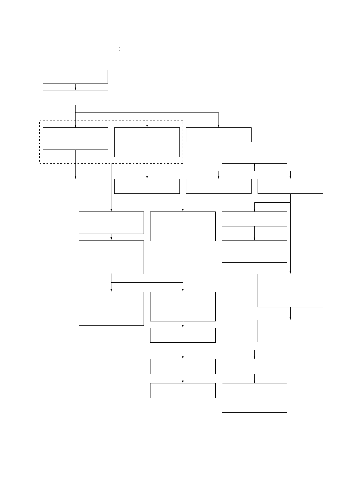
1. PARTS REPLACEMENT AND ADJUSTMENT
If malfunctions caused by optical pick-up such as sound skipping are suspected, follow the following check.
Check before replacement
Start
6-2.
Laser Power Check
(See page 37)
OK
6-3.
Iop Compare
(See page 37)
OK
6-4.
Auto Check
(See page 38)
OK
Other faults are suspected.
Check the mechanism parts (spindle motor, sled motor, etc.).
NG
NG
NG
Replace optical pick-up or MDM-7B4B
34
Page 35

Adjustment flow
Start
HCD-C5
• Abbreviation
OP: optical pick-up
Replace IC195
NO
Replace OP or IC195
NO
Replace IC101, IC195, or D101
NO
Replace OP, IC190, or IC195
NO
YES
YES
YES
YES
After turning off and then on the power,
initialize the EEPROM
For details, refer to “WHEN MEMORY NG IS DIS-
PLAYED” in Section 4. TEST MODE (See page 29)
7.INITIAL SETTING OF ADJUSTMENT VALUE
(See page 40)
9.TEMPERATURE COMPENSATION OFFSET
ADJUSTMENT (See page 40)
10. LASER POWER ADJUSTMENT (See page 40)
Replace OP, IC102, IC190,
or IC195
NO
Replace OP, IC101, IC151,
or IC195
NO
Replace OP
NO
6-4. Auto Check
(See page 38)
End adjustments
YES
YES
YES
11. Iop NV SAVE (See page 41)
12.TRAVERSE ADJUSTMENT (See page 41)
13.FOCUS BIAS ADJUSTMENT (See page 43)
16.AUTO GAIN CONTROL OUTPUT LEVEL
ADJUSTMENT (See page 44)
8.RECORDING AND DISPLAYING THE IOP
INFORMATION (See page 40)
35
Page 36

HCD-C5
d
2. PRECAUTIONS FOR CHECKING LASER DIODE
EMISSION
T o check the emission of the laser diode dur ing adjustments, ne ver
view directly from the top as this may lose your eye-sight.
3.
PRECAUTIONS FOR USE OF OPTICAL PICK-UP
(KMS-260B/260E)
As the laser diode in the optical pick-up is easily damaged by static
electricity, solder the laser tap of the flexible board when handling
it.
Before disconnecting the connector, solder first. Befor e connecting
the connector, be careful not to remov e the solder. Also take adequate
measures to prevent damage by static electricity . Handle the flexible
board with care as it breaks easily.
pick-up
flexible boar
4. PRECAUTIONS FOR ADJUSTMENTS
1. When replacing the following parts, perform the adjustments
and checks with
2. Set the MD test mode when performing adjustments.
After completing the adjustments, exit the MD test mode.
Perform the adjustments and checks in “Group Service” of the
MD test mode.
3. Perform the adjustments to be needed in the order shown.
4. Use the following tools and measuring devices.
• Check Disc (TDYS-1) (Part No. : 4-963-646-01)
• Test Disk (MDW-74/GA-1) (Part No. : 4-229-747-01)
• Laser power meter LPM-8001 (Part No. : J-2501-046-A)
or MD Laser power meter 8010S (Part No. : J-2501-145-A)*
• Oscilloscope (Measure after performing CAL of prove.)
• Digital voltmeter
• Thermometer
• Jig for checking BD (MD) board waveform
(Part No. : J-2501-196-A)
5. When observing several signals on the oscilloscope, etc.,
make sure that VC and ground do not connect inside the
oscilloscope.
(VC and ground will become short-circuited.)
6. Using the above jig enables the waveform to be check ed without
the need to solder.
(Refer to Servicing Notes on page 6.)
7. As the disc used will affect the adjustment results, make sure
that no dusts nor fingerprints are attached to it.
in the order shown in the following table.
1
Optical pick-up flexible board
Adjustment
7. Initial setting of adjustment value
8. Recording of Iop information
9. Temperature compensation
offset adjustment
10. Laser power adjustment
11. Iop NV Save
12. Traverse adjustment
13. Focus bias adjustment
16. Auto gain control output level
adjustment
6-4.AUTO CHECK
laser tap
Optical
Pick-up
*1Laser power meter
When performing laser power checks and adjustment (electrical
adjustment), use of the new MD laser power meter 8010S (Part
No. J-2501-145-A) instead of the conventional laser power
meter is convenient.
It sharply reduces the time and trouble to set the laser power
meter sensor onto the objective lens of optical pick-up.
Parts to be replaced
IC101 IC102 IC151 IC190 IC195 D101
36
Page 37

HCD-C5
r
r
KMS260B
20101
H0576
lOP = 57.6 mA in this case
lOP (mA) = Digital voltmeter reading (mV)/1 (
Ω
)
(Optical pick-up label)
For details of the method for
checking this value, refer to
“8. Recording and Displaying
the Iop Information”
5. USING THE CONTINUOUSLY RECORDED DISC
* This disc is used in focus bias adjustment and error rate check.
The following describes how to create a continuous recording
disc.
1. Insert a disc (blank disc) commercially available.
2. Press the . “R” or > “R” button and display “CREC 1MODE”
(C35).
3. Press the ENTER/YES “R” button again to display “CREC 1
MID”.
Display “CREC 1(0300)” and start to recording.
4. Complete recording within 5 minutes.
5. Press the MENU/NO “R” button and stop recording .
6. Press the MD Z button and remove the disc.
The above has been how to create a continuous recorded data for
the focus bias adjustment and error rate check.
Note: Be careful not to apply vibration during continuous recording.
6. CHECKS PRIOR TO REPAIRS
These checks are performed before replacing parts according to
“approximate specifications” to determine the faulty locations. For
details, refer to “Checks Prior to Parts Replacement and Adjustments
in MD” (see page 30).
Procedure:
1. Set the laser power meter on the objective lens of the optical
pick-up. (When it cannot be set properly, press the m “R” button
or M “R” button to move the optical pick-up.)
Connect the digital volt meter to CN105 pin 1 (I+3V) and
CN105 pin 2 (IOP).
2. Then, press the . “R” or > “R” button and display
“LDPWR CHECK” (C13).
3. Press the ENTER/YES “R” button once and display “LD 0.9mW$
”. Check that the reading of the laser power meter becomes
specified value.
SPECIFIED VALUE
KMS-260B
KMS-260E
0.85 to 0.91 mW
0.90 to 0.96 mW
4. Press the ENTER/YES “R” button once more and display “ LD
7.0mW$ ”. Check that the reading the laser power meter and
digital volt meter satisfy the specified value.
Specified V alue:
Laser power meter reading :
KMS-260B
KMS-260E
7.0 to 0.2 mW
7.25 to 0.25 mW
Digital voltmeter reading : Optical pick-up displayed value ± 10%
6-1. Temperature Compensation Offset Check
When performing adjustments, set the internal temperature and room
temperature to 22 to 28ºC.
Procedure:
1. Press the
. “R” or > “R” button to display “TEMP
CHECK” (C12).
2. Press the ENTER/YES “R” button.
3. “T=@@(##) [OK]” should be displayed. If “T=@@ (##) [NG]”
is displayed, it means that the results are bad.
(@@ indicates the current value set, and ## indicates the value
written in the non-volatile memory.)
6-2. Laser Power Check
Before starting adjustment;
The laser power adjustment value changes depending upon the types
of the optical pick-up (KMS-260B or KMS-260E).
Check the type of the optical pick-up before starting adjustment.
(See the illustrations “The method of identifying the optical pickup” on page 41)
Before checking, check the Iop value of the optical pick-up.
(Refer to 8. Recording and Displaying the Iop Information (see page
40))
Connection:
laser
power mete
5. Press the MENU/NO “R” button and display “LDPWR
CHECK” (C13) and stop the laser emission.
(The MENU/NO “R” b utton is ef fecti v e at all times to stop the
laser emission.)
Note: After step 4, each time the ENTER/YES “R” button is pressed, the
display will be switched to “LD 0.7W$ ”and “LD 6.2mW$ ”
“LD WP $ ”. Nothing needs to be performed here.
Checking Location: BD (MD) board (see page 44)
6-3. Iop Compare
The current Iop value at laser power 7.0 mW output and reference
Iop value (set at shipment) written in the nonvolatile memory are
compared, and the rate of increase/decrease will be displayed in
percentage.
Note: Perform this function with the optical pick-up set at room tempera-
ture.
Optical pick-up
objective lens
BD (MD) board
CN105 pin 1 (I+3V)
CN105 pin 2 (IOP)
Procedure:
1. Press the . “R” or > “R” button to display “Iop Compare”
(C27).
2. Press the ENTER/YES “R” button and start measurements.
digital voltmete
3. When measurements complete, the display changes to “± xx%
yy”.
xx is the percentage of increase/decrease, and OK or NG is
displayed at yy to indicate whether the percentage of increase/
+
–
decrease is within the allowable range.
4. Press the MENU/NO “R” button to end.
37
Page 38

HCD-C5
+
–
oscilloscope
(DC range)
V: 0.1 V/div
H: 10 ms/div
BD (MD) board
CN105 pin 4 (TE)
CN105 pin 6 (VC)
6-4. Auto Check
This test mode performs CREC and CPLAY automatically for
mainly checking the characteristics of the optical pick-up. T o perform
this test mode, the laser power must first be check ed. Perform Auto
Check after the laser power check and Iop compare.
Procedure:
1. Press the . “R” or > “R” button to display “AUTO CHECK”
(C01).
2. Press the ENTER/YES “R” button. If “LDPWR ” is
displayed, it means that the laser power check has not been
performed. In this case, perform the laser power check and Iop
Compare, and then repeat from enter the MD test mode.
3. If a disc is in the mechanical deck, it will be ejected forcibly.
“DISC IN” will be displayed in this case. Load a test disc (MDW 74/GA-1) which can be recorded.
4. If a disc is loaded at step 3, the check will start automatically.
5. When “XX CHECK” is displayed, the item corresponding to
XX will be performed.
When “06 CHECK” completes, the disc loaded at step 3 will be
ejected. “DISC IN” will be displayed. Load the check disc
(TDYS-1).
6. When the disc is loaded in the step 5, the check will automatically
be resumed from “07 CHECK”.
7. After completing to test item 12 (“oC CHECK”), check OK or
NG will be displayed. If all items are OK, “CHK ALL OK” will
be displayed. If any item is NG, it will be displayed as
“NG:xxxx”.
When “CHK ALL OK” is displayed, it means that the optical pickup is normal. Check the operations of other parts (spindle motor,
sled motor, etc.).
When displayed as “NG:xxxx”, it means that the optical pick-up is
faulty. In this case, replace the optical pick-up.
6-5. Other Checks
All the following checks are performed by the Auto Check mode.
They therefore need not be performed in normal operation.
6-6. Traverse Check
6-7. Focus Bias Check
6-8. C PLAY Check
6-9. Self-Recording/Playback Check
6-6. Traverse Check
Note 1:Data will be erased during MO reading if a recorded disc is
used in this adjustment.
Note 2:If the traverse waveform is not clear, connect the oscilloscope
as shown in the following figure so that it can be seen more
clearly.
oscilloscope
(DC range)
BD (MD) board
CN105 pin 4 (TE)
CN105 pin
6
(VC)
330 k
Ω
+
–
10 pF
Connection:
Procedure:
1. Connect an oscilloscope to CN105 pin 4 (TE) and CN105 pin
6 (VC) on the BD (MD) board.
2. Load a disc (any available on the market). (Refer to Note 1)
3. Press the M “R” button to move the optical pick-up outside
the pit.
4. Press the . “R” or > “R” button to display “EF MO
CHECK”(C14).
5. Press the ENTER/YES “R” button to display “EFB = MOR”. (Laser power READ power/Focus serv o ON/tracking servo
OFF/spindle (S) servo ON)
6. Observe the waveform of the oscilloscope, and check that the
specified value is satisfied. Do not press the . “R” or
> “R” button.
(Read power traverse checking)
Traverse Waveform
38
A
VC
B
Specified value : Below 10% offset value
I
A – B
Offset value (%) = X 100
I
2 (A + B)
7. Press the ENTER/YES “R” button to display “EFB = MO-
W”.
8. Observe the waveform of the oscilloscope, and check that the
specified value is satisfied. Do not press the . “R” or
> “R” button. (Write power traverse checking)
Traverse Waveform
A
VC
B
Specified value : Below 10% offset value
I
A – B
Offset value (%) = X 100
I
2 (A + B)
Page 39

HCD-C5
9. Press the ENTER/YES “R” button to display “EFB = MO-
P”.
Then, the optical pick-up moves to the pit area automatically
and servo is imposed.
10. Observe the waveform of the oscilloscope, and check that the
specified value is satisfied. Do not press the . “R” or
> “R” button.
Traverse Waveform
A
VC
B
Specified value : Below 10% offset value
I
A – B
Offset value (%) = X 100
I
2 (A + B)
11. Press the ENTER/YES “R” button to display “EF MO CHECK”
(C14).
The disc stops rotating automatically.
12. Press the MD Z button and take out the disc.
13. Load the check disc (TDYS-1).
14. Press the . “R” or > “R” button and display “EF CD
CHECK” (C15).
15. Press the ENTER/YES “R” button to display “EFB = CD”.
Servo is imposed automatically.
16. Observe the waveform of the oscilloscope, and check that the
specified value is satisfied. Do not press the . “R” or
> “R” button.
Traverse Waveform
A
VC
B
Specified value : Below 10% offset value
I
A – B
Offset value (%) = X 100
I
2 (A + B)
17. Press the ENTER/YES “R” button to display “EF CD
CHECK” (C15).
18. Press the MD Z button and take out the check disc (TDYS-1).
Checking Location: BD (MD) board (see page 44)
6-7. Focus Bias Check
Change the focus bias and check the focus tolerance amount.
Procedure:
1. Load the test disc (MDW-74/GA-1).
2. Press the . “R” or > “R” button to display “CPLAY
1MODE” (C34).
3. Press the ENTER/YES “R” button to display “CPLA Y 1MID”.
4. Press the MENU/NO “R” button when “C = AD =
” is displayed.
5. Press the . “R” or > “R” button to display “FBIAS
CHECK” (C16).
6. Press the ENTER/YES “R” button to display “ / c =
”.
The first four digits indicate the C1 error rate, the two digits
after [/] indicate ADER, and the 2 digits after [c =] indicate the
focus bias value.
Check that the C1 error is below 20 and ADER is below 2.
7. Press the ENTER/YES “R” button to display “ / b =
”.
Check that the C1 error is about 100 and ADER is below 2.
8. Press the ENTER/YES “R” button to display “ / a =
”.
Check that the C1 error is about 100 and ADER is below 2.
9. Press the MENU/NO “R” button, then press the MD Z button
and take out the test disc.
6-8. C PLAY Check
MO Error Rate Check
Procedure:
1. Load the test disc (MDW-74/GA-1).
2. Press the . “R” or > “R” button to display “CPLAY
1MODE” (C34).
3. Press the ENTER/YES “R” button to display “CPLA Y 1MID”.
4. The display changes to “C = AD = ”.
5. If the C1 error rate is below 20, check that ADER is 00.
6. Press the MENU/NO “R” button to stop playback, then press
the MD Z button and take out the test disc.
CD Error Rate Check
Procedure:
1. Load the check disc (TDYS-1).
2. Press the . “R” or > “R” button to display “CPLAY
1MODE” (C34).
3. Press the ENTER/YES “R” button to display “CPLA Y 1MID”.
4. The display changes to “C =
AD = )”.
5. Check that the C1 error rate is below 20.
6. Press the MENU/NO “R” button to stop playback, then press
the MD Z button and take out the check disc.
6-9. Self-Recording/playback Check
Prepare a continuous recording disc using the unit to be repaired
and check the error rate.
Procedure:
1. Load a recordable disc (blank disc).
2. Press the . “R” or > “R” button to display “CREC
1MODE” (C34).
3. Press the ENTER/YES “R” button to display “CREC 1MID”.
4. When recording starts, “ REC ” and display “CREC 1 @@@@”
REC
(@@@@ is the address).
5. About 1 minute later, press the MENU/NO “R” button to stop
continuous recording.
6. Press the . “R” or > “R” button to display “CPLAY
1 MODE” (C34).
7. Press the ENTER/YES “R” button to display “CPLAY 1
MID”.
8. “C = AD = )” will be displayed.
9. Check that the C1 error becomes below 20 and the AD error
below 2.
10. Press the MENU/NO “R” button to stop playback, then press
the MD Z button and take out the disc.
39
Page 40

HCD-C5
+
–
BD (MD) board
digital voltmeter
CN105 pin 1 (I+3V)
CN105 pin
2
(IOP)
7. INITIAL SETTING OF ADJUSTMENT VALUE
Note:
Mode which sets the adjustment results recorded in the non-volatile memory
to the initial setting value. However the results of the temperature compensation offset adjustment will not change to the initial setting value.
If initial setting is performed, perform all adjustments again excluding the
temperature compensation offset adjustment.
For details of the initial setting, refer to “4. Precautions for Adjustments”
(See page 36) and execute the initial setting before the adjustment as required.
Procedure:
1. Press the . “R” or > “R” button to display “ADJ
CLEAR” (C28).
2. Press the ENTER/YES “R” button. “Complete!” will be
displayed momentarily and initial setting will be executed, after
which “ADJ CLEAR” (C28) will be displayed.
8. RECORDING AND DISPLAYING THE IOP
INFORMATION
The IOP data can be recorded in the non-volatile memory . The IOP
value on the optical pick-up label and the IOP value after the
adjustment will be recorded. Recording these data eliminates the
need to read the label on the optical pick-up.
Recording Procedure:
1. Press the . “R” or > “R” button to display “Iop Write”
(C05), and press the ENTER/YES “R” button.
2. The display becomes “Ref=@@@.@” (@ is an arbitrary
number) and the numbers which can be changed will blink.
3. Input the IOP value on the optical pick-up label.
To select the number : Press the . “R” or > “R” b utton.
To select the digit : Press two buttons of VOL - and
CD Z simultaneously.
4. When the ENTER/YES “R” button is pressed, the display
becomes “Measu=@@@.@” (@ is an arbitrary number).
5. As the adjustment results are recorded for the step 4 value. Leave
it as it is and press the ENTER/YES “R” button.
6. “Complete!” will be displayed momentarily. The value will be
recorded in the non-volatile memory and the display will become
“Iop Write” (C05).
Procedure:
1. Press the . “R” or > “R” button to display “TEMP
ADJUST” (C03).
2. Press the ENTER/YES “R” button to select the “TEMP
ADJUST” mode.
3. “TEMP = [OK]” and the current temperature data will be
displayed.
4. To save the data, press the ENTER/YES “R” button.
When not saving the data, press the MENU/NO “R” button.
5. When the ENTER/YES “R” button is pressed, “TEMP =
SAVE” will be displayed and turned back to “TEMP ADJUST”
(C03) display then. When the MENU/NO “R” button is pressed,
“TEMP ADJUST” (C03) will be displayed immediately.
Specified V alue:
The “TEMP = ” should be within “E0 - EF”, “F0 - FF”, “00 0F”, “10 - 1F” and “20 - 2F”.
10.LASER POWER ADJUSTMENT
Before starting adjustment;
The laser power adjustment value changes depending upon the types
of the optical pick-up (KMS-260B or KMS-260E).
Check the type of the optical pick-up before starting adjustment.
(See the illustrations “The method of identifying the optical pickup on page 41.)
Check the IOP value of the optical pick-up before adjustments.
(Refer to 8. Recording and Displaying the Iop Information)
Connection:
Optical pick-up
objective lens
laser
power meter
Display Procedure:
1. Press the . “R” or > “R” button to display “Iop
Read”(C26) and press the ENTER/YES “R” button.
2. “@@.@/##.#” is displayed and the recorded contents are
displayed.
@@.@ indicates the IOP value on the optical pick-up label.
##.# indicates the IOP value after adjustment
3. To end, press the MENU/NO “R” button to display “Iop Read”
(C26).
9. TEMPERATURE COMPENSATION OFFSET
ADJUSTMENT
Save the temperature data at that time in the non-volatile memory
as 25 ˚C reference data.
Note:
1. Usually, do not perform this adjustment.
2. Perform this adjustment in an ambient temperature of 22 ˚C to 28 ˚C. Per-
form it immediately after the power is turned on when the internal temperature of the unit is the same as the ambient temperature of 22 ˚C to 28 ˚C.
3. When D101 has been replaced, perform this adjustment after the tem-
perature of this part has become the ambient temperature.
40
Procedure:
1. Insert the laser power meter probe into the disc insertion slot
and set it on top of the objective lens of the optical pick-up.
(When it cannot be set properly, press the
M “R” button to move the optical pick-up)
m “R” button or
Connect the digital voltmeter to CN105 pin 1 (I+3V) and
CN105pin 2 (IOP) on the BD (MD) board.
2. Press the . “R” or > “R” button to display “LDPWR
ADJUST” (C04).
(Laser power : For adjustment)
3. Press the ENTER/YES “R” button once to display “LD 0.9 mW
$ ”.
4. Press the . “R” or > “R” button until the laser power
meter reading matches with the specified value as described in
the following table.
SPECIFIED VALUE
KMS-260B
KMS-260E
0.85 to 0.91 mW
0.90 to 0.96 mW
Press the ENTER/YES “R” button after setting the range knob
of the laser power meter, and save the adjustment results.
(“LD SAVE $ ” will be displayed for a moment)
5. Then “LD 7.0 mW $ ” will be displayed.
Page 41

HCD-C5
UV adhesive agent
Optical pick-up
(KMS-260B/260E)
Pink : KMS-260B
White : KMS-260E
UV adhesive agent =
+
–
oscilloscope
(DC range)
10 pF
330 k
Ω
CN105 pin 4 (TE)
CN105 pin
6
(VC)
BD (MD) board
6. Press the . “R” or > “R” button so that the reading
of the laser power meter becomes the specified value, pr ess the
ENTER/YES “R” button to save it.
SPECIFIED VALUE
Note: Do not perform the emission with 8.4 mW more than 15 seconds
continuously.
KMS-260B
KMS-260E
6.9 to 7.1 mW
7.2 to 7.3 mW
7. Then, press the . “R” or > “R” button to display
“LDPWR CHECK” (C13).
8. Press the ENTER/YES “R” button once to display “LD
0.9mW$ ”. Check that the reading of the laser power meter
matches with the specified value as described in the following
table.
SPECIFIED VALUE
KMS-260B
KMS-260E
0.85 to 0.91 mW
0.90 to 0.96 mW
9. Press the ENTER/YES “R” button once more to display “LD
8.4mW$ ”. Check that the reading the laser power meter and
digital voltmeter satisfy the specified value.
Note down the digital voltmeter reading value.
Specified V alue:
Laser power meter reading :
SPECIFIED VALUE
Digital voltmeter reading :
(Optical pick-up label)
KMS260B
20101
H0576
lOP = 57.6 mA in this case
lOP (mA) = Digital voltmeter reading (mV)/1 (
KMS-260B
KMS-260E
Value on the optical pick-up label ±10%
For details of the method for
checking this value, refer to
“8. Recording and Displaying
the Iop Information”
7.0 to 0.2 mW
7.25 to 0.25 mW
Ω
)
10. Press the MENU/NO “R” button to display “LDPWR CHECK”
(C13) and stop the laser emission.
(The MENU/NO “R” button is effecti ve at all times to stop the
laser emission)
11. Press the . “R” or > “R” button to display “Iop Write”
(C05).
12. Press the ENTER/YES “R” button. When the display becomes
“Ref=@@@.@” (@ is an arbitrary number), press the
ENTER/YES “R” button to display “Measu=@@@.@” (@ is
an arbitrary number).
13. The numbers which can be changed will blink. Input the Iop
value noted down at step 9.
T o select the number : Press the . “R” or > “R” button.
T o select the digit :Press two buttons of VOL - and
CD Z simultaneously.
14.
When the ENTER/YES “R” button is pressed, “Complete!” will
be displayed momentarily. The value will be recorded in the nonvolatile memory and the display will become “Iop Write” (C05).
Note: After step 9, each time the ENTER/YES “R” button is pressed, the
display will be switched to “LD 0.7mW$ ”, “LD 6.2mW$ ”
and “LD WP ” Nothing needs to be performed here.
The method of identifying the optical pick-up
(KMS-260B/260E)
11.Iop NV SAVE
Write the reference values in the nonvolatile memory to perform
“Iop compare”. As this involves rewriting the reference values, do
not perform this procedure except when adjusting the laser power
during replacement of the optical pick-up and when replacing the
IC102. Otherwise the optical pick-up check may deteriorate.
Note:
Perform this function with the optical pick-up set at room temperature.
Procedure:
1.
Press the . “R” or > “R” button to display “Iop NV Save”
(C06).
2. Press the ENTER/YES “R” button and display “Iop [stop]”.
3. After the display changes to “Iop =xxsave?”, press the
ENTER/YES “R” button.
4. After “Complete!” is displa yed momentarily, the display chang es
to “Iop 7.0 mW”.
5. After the display changes to “Iop=yysave?”, press the
ENTER/YES “R” button.
6. When “Complete!” is displayed, it means that Iop NV saving
has been completed.
12. TRAVERSE ADJUSTMENT
Note 1: Data will be erased during MO reading if a recorded disc is
used in this adjustment.
Note 2: If the traverse waveform is not clear, connect the oscilloscope
as shown in the following figure so that it can be seen more
clearly.
Connection:
oscilloscope
(DC range)
BD (MD) board
CN105 pin 4 (TE)
CN105 pin 6 (VC)
+
–
V: 0.1 V/div
H: 10 ms/div
41
Page 42

HCD-C5
Procedure:
1. Connect an oscilloscope to CN105 pin 4 (TE) and CN105 pin
6 (VC) on the BD (MD) board.
2. Load a disc (any available on the market). (Refer to Note 1)
3. Press the M “R” button to move the optical pick-up outside
the pit.
4. Press the . “R” or > “R” button to display “EF MO
ADJUST” (C07).
5.
Press the ENTER/YES “R” button to display “EFB = MOR”.
(Laser power READ power/Focus serv o ON/tracking servo
OFF/spindle (S) servo ON)
6. Press the . “R” or > “R” button so that the waveform of
the oscilloscope becomes the specified value.
(When the . “R” or > “R” button is pressed, the of
“EFB= ” changes and the waveform changes) In this adjustment,
waveform varies at intervals of approx. 2%. Adjust the waveform
so that the specified value is satisfied as much as possible.
(Read power traverse adjustment)
Traverse Waveform
A
VC
B
Specification A = B
7. Press the ENTER/YES “R” button and save the result of
adjustment to the non-volatile memory (“EFB = SAVE”
will be displayed for a moment. Then “EFB = MO-W” will
be displayed).
8. Press the . “R” or > “R” button so that the waveform of
the oscilloscope becomes the specified value.
(When the . “R” or > “R” b utton is pressed, the
of
“EFB= ” changes and the waveform changes) In this
adjustment, waveform varies at interv als of approx. 2%. Adjust
the waveform so that the specified v alue is satisf ied as much as
possible. (Write power traverse adjustment)
Traverse Waveform
A
VC
B
11. Press the . “R” or > “R” button until the waveform of
the oscilloscope moves closer to the specified value.
In this adjustment, waveform varies at interv als of approx. 2%.
Adjust the waveform so that the specified value is satisfied as
much as possible.
Traverse Waveform
A
VC
B
Specification A = B
12. Press the ENTER/YES “R” button, and save the adjustment
results in the non-volatile memory. (“EFB = SAVE” will be
displayed for a moment)
Next “EF MO ADJUST” (C07) is displayed. The disc stops
rotating automatically.
13. Press the MD Z button and take out the disc.
14. Load the check disc (TDYS-1).
15. Press the . “R” or > “R” button to display “EF CD
ADJUST” (C08).
16. Press the ENTER/YES “R” button to display “EFB = CD”.
Servo is imposed automatically.
17. Press the . “R” or > “R” button so that the waveform of
the oscilloscope moves closer to the specified value.
In this adjustment, waveform varies at interv als of approx. 2%.
Adjust the waveform so that the specified value is satisfied as
much as possible.
Traverse Waveform
A
VC
B
Specification A = B
18. Press the ENTER/YES “R” button, display “EFB = SA VE”
for a moment and save the adjustment results in the non-volatile
memory.
Next “EF CD ADJUST” (C08) will be displayed.
19. Press the MD Z button and take out the check disc.
Specification A = B
9. Press the ENTER/YES “R” button, and save the adjustment
results in the non-volatile memory . (“EFB = SA VE” will be
displayed for a moment)
10. “EFB = MO-P” will be displayed.
The optical pick-up moves to the pit area automatically and
servo is imposed.
42
Adjustment Location: BD (MD) board (see page 44)
Page 43

HCD-C5
13. FOCUS BIAS ADJUSTMENT
Procedure:
1. Load the continuously-recorded disc. (Refer to “5. USING
THE CONTINUOUSLY RECORDED DISC” (See page 37))
2. Press the . “R” or > “R” button to display “CPLAY 1
MODE” (C34).
3. Press the ENTER/YES “R” button to display “CPLA Y 1MID”.
4. Press the MENU/NO “R” button when “C = = ” is
displayed.
5. Press the . “R” or > “R” button to display “FBIAS
ADJUST” (C09).
6. Press the ENTER/YES “R” button to display “ / a =
T”.
The first four digits indicate the C1 error rate, the two digits
after “/ ” indicate ADER, and the 2 digits after “a =” indicate
the focus bias value.
7. Press the > “R” button and find the focus bias value at
which the C1 error rate becomes about 220 (refer to Note 2).
8. Press the ENTER/YES “R” button to display “ / b =
T”.
9. Press the . “R” button and find the focus bias value at
which the C1 error rate becomes about 220.
10. Press the ENTER/YES “R” button to display “ / c =
T”.
11. Check that the C1 error rate is below 20 and ADER is 00. Then
press the ENTER/YES “R” button.
12. If the “( )” in “ - - ( )” is above 20, press the
ENTER/YES “R” button.
If below 20, press the MENU/NO “R” button and repeat the
adjustment from step 2.
13. Press thet MD Z button and take out the disc.
Note 1: The relation between the C1 error and focus bias is as shown in
Note 2: As the C1 error rate changes, perform the adjustment using the
the following figure. Find points A and B in the follo wing figure
using the above adjustment. The focal point position C is automatically calculated from points A and B.
average value.
C1 error
about
220
Focus bias value
B
CA
14. ERROR RATE CHECK
14-1. CD Error Rate Check
Procedure:
1. Load the check disc (TDYS-1).
2. Press the . “R” or > “R” button and display “CPLA Y 1
MODE” (C34).
3. Pr ess the ENTER/YES “R” button and display “CPLAY 1
MID”.
4. The display changes to “C = AD = )”.
5. Check that the C1 error rate is below 20.
6. Press the MENU/NO “R” button to stop playback, then press
the MD Z button and take out the check disc.
14-2. MO Error Rate Check
Procedure:
1. Load the continuously-recorded disc. (Refer to “5. USING THE
CONTINUOUSLY RECORDED DISC” (See page 37))
2. Press the . “R” or > “R” button to display “CPLAY 1
MODE” (C34).
3. Press the ENTER/YES “R” button to display “CPLA Y 1MID”.
4. The display changes to “C1 = AD = )”.
5. If the C1 error rate is below 20, check that ADER is 00.
6. Press the MENU/NO “R” button to stop playback, then press
the MD Z button and take out the disc.
15. FOCUS BIAS CHECK
Change the focus bias and check the focus tolerance amount.
Procedure:
1. Load the continuously-recorded disc. (Refer to “5. USING
THE CONTINUOUSLY RECORDED DISC” (See page 37))
2. Press the . “R” or > “R” button to display “CPLAY 1
MODE” (C34).
3. Press the ENTER/YES “R” button twice to display “CPLAY
1 MID”.
4. Press the MENU/NO “R” button when “C1 =
)” is displayed.
5. Press the . “R” or > “R” button to display “FBIAS
CHECK” (C16).
6. Press the ENTER/YES “R” button to display “ / c =
”.
The first four digits indicate the C1 error rate, the two digits
after “/ ” indicate ADER, and the 2 digits after “c =” indicate
the focus bias value.
Check that the C1 error is below 20 and ADER is below 2.
7. Press the ENTER/YES “R” button and display “ / b
= ”.
Check that the C1 error is about 100 and ADER is below 2.
8. Press the ENTER/YES “R” button and display “ / a
= ”.
Check that the C1 error is about 100 and ADER is below 2
9. Press the MENU/NO “R” button, then press the MD Z button
and take out the disc.
AD =
Note: If the C1 error and ADER are above other than the specified
value at points a (step 8. in the above) or b (step 7. in the abov e),
the focus bias adjustment may not have been carried out properly. Adjust from the beginning again.
43
Page 44

HCD-C5
16. AUTO GAIN CONTROL OUTPUT LEVEL ADJUSTMENT
Be sure to perform this adjustment when the optical pick-up is replaced.
If the adjustment results becomes “Adjust NG!”, the optical pick-up may be faulty or the servo system circuits may be abnormal.
16-1. CD Auto Gain Control Output Level Adjustment
Procedure:
1. Load the check disc (TDYS-1).
2. Press the . m “R” or M > “R” button to display “AG Set (CD)” (C11).
3. When the ENTER/YES “R” button is pressed, the adjustment will be performed automatically.
“Complete!” will then be displayed momentarily when the value is recorded in the non-volatile memory, after which the
display changes to “AG Set (CD)” (C11).
4. Press the MD Z button and take out the check disc.
16-2. MO Auto Gain Control Output Level Adjustment
Procedure:
1. Load the test disc (MDW-74/GA-1).
2. Press the . “R” or > “R” button to display “AG Set (MO)” (C10).
3. When the ENTER/YES “R” button is pressed, the adjustment will be performed automatically.
“Complete!” will then be displayed momentarily when the value is recorded in the non-volatile memory, after which the
display changes to “AG Set (MO)” (C10).
4. Press the MD Z button and take out the test disc.
Adjustment and checking Loacation:
– BD (MD) BOARD (Component Side) –
D101
CN101
Note: It is useful to use the jig for checking the waveform. (Refer to Servicing Notes on page 6)
– BD (MD) BOARD (Conductor Side) –
IC190
IC151
IC101
CN105
1
7
1. I+3V
2. IOP
3. GND
4. TE
5. FE
6. VC
7. RF
44
Page 45

SECTION 6
d
d
DIAGRAMS
HCD-C5
Ver 1.1 2001.09
6-1. NOTE FOR PRINTED WIRING BOARDS AND SCHEMATIC DIAGRAMS
(In addition to this, the necessary note is printed in each block)
Note on Printed Wiring Boards:
• X : parts extracted from the component side.
a
•
• Y : parts extracted from the conductor side.
• b : Pattern from the side which enables seeing.
Caution:
Pattern face side: Parts on the pattern face side seen from
(Conductor B) the pattern face are indicated.
Parts face side: Parts on the parts face side seen from
(Component A) the parts face are indicated.
(The other layers' patterns are not indicated.)
• Indication of transistor.
• Abbreviation
: Through hole.
C
Q
B
E
B
AUS : Australian model
HK : Hong Kong model
KR : Korean model
These are omitted.
Q
CE
These are omitted.
Note on Schematic Diagram:
• All capacitors are in µF unless otherwise noted. pF: µµF
50 WV or less are not indicated except for electrolytics
and tantalums.
• All resistors are in Ω and 1/
specified.
• 5 : fusible resistor.
• C : panel designation.
• A : B+ Line.
• B : B– Line.
Note: The components identified by mark 0 or dotted line
with mark 0 are critical for safety.
Replace only with part number specified.
• Voltages are taken with a VOM (Input impedance 10 MΩ).
Voltage variations may be noted due to normal production tolerances.
• Waveforms are taken with a oscilloscope.
Voltage variations may be noted due to normal production tolerances.
• Circled numbers refer to waveforms.
• Signal path.
F : FM
J : CD (ANALOG)
c : CD (DIGITAL)
p : PB (MD)
l : REC (MD)
I : DIGITAL IN (OPTICAL)
E : PB (TAPE)
G : REC (TAPE)
4
W or less unless otherwise
• Circuit Boards Location
POWER board
PANEL board
HP board
JACK boar
AUDIO board
• Waveforms
1
IC101 us XTAO
29.5 µs
5
IC151 o; (FS4)
176.4kHz
4.0Vp-p
VOLT/DIV : 1V AC
TIME/DIV : 20 nsec
3.5Vp-p
2
IC101 ek (RF)
6
IC701 qd XOUT
100 ns
1.3Vp-p
3.2 Vp-p
VOLT/DIV : 1V AC
TIME/DIV : 40 nsec
3
IC101 ef (FE)
(Play mode)
7
IC501 eh XT2
30.5 µs
VOLT/DIV : 1V AC
TIME/DIV : 20
0.2Vp-p
3.2Vp-p
µ
4
IC101 wh (TE)
(Play mode)
8
IC501 ek X2
sec
50 ns
VOLT/DIV : 1V AC
TIME/DIV : 40 nsec
1.6Vp-p
3.1 Vp-p
SW board
CONNECTOR board
AMP POWER boardUCOM board
BD (CD) boar
BD (MD) board MD DIGITAL board
4545
Page 46

HCD-C5
6-2. BLOCK DIAGRAM – CD SERVO SECTION –
• Signal Path
: CD (DIGITAL)
:DIGITAL IN (OPTICAL)
OPTICAL PICK-UP
BLOCK
OPTIMA-720L1E
1/2VCC
9
VCC
8
VA
4
VB
6
VC
2
VE
3
VF
7
LD
10
GND
5
MD
1
VR
F+
FOCUS
COIL
TRACKING
COIL
F-
TR+
TR-
+5V
Q101
LD
DRIVE
M903
FEED
MOTOR
M904
SPINDLE
MOTOR
RV101
M
M
27
25
7
6
8
9
10
11
1
VCC
19 TE_BAL
2
MOTOR/COIL DRIVER
14
VO1(+)
13
VO1(-)
12
VO2(+)
11
VO2(-)
SD+
15
VO4(+)
SD-
16
VO4(-)
SP+
18
VO3(-)
SP-
17
VO3(+)
VC
VFC
B
A
C
D
E
F
LD
PD
IC103
RF AMP
RFAC
RFDCO
RFDCI
IC102
OPIN1(+)
OPIN1(-)
OPIN2(+)
OPIN(2-)
OPIN4(+)
OPIN4(-)
OPIN3(-)
+5V
Q102
SWITCH
26
RFC
15
28
16FE
18TE
SW
12
FEI
17
29
S5
LIMIT
IN
2
3
5
6
27
26
23 MDP
SWITCH
IC221
D OUT
XTSL
DATA
CLOK
XLAT
SQSO
SENS
SCLK
SQCK
SCOR
XRST
XTAI
XTAO
DIGITAL
OPTICAL
64
69
4
6
5
76
7
8
77
15
2
71
72
DIGITAL
OPTICAL
INPUT
IC101
DIGITAL SERVO,
DIGITAL SIGNAL PROCESSOR
50
RFAC
43
RFDC
39
FE
41
TE
40
SE
26 SSTP
33
FFDR
34
FRDR
31
TFDR
32
TRDR
29
SFDR
30
SRDR
25
IN
CTRL1(1-2)
DATA
CLK
XLT
SQSO
SENS
SCLK
SCOR
XRST
X201
33.8688MHz
LDON
IC222
SELECTOR
5
1
3
2
13
12
S1 (Disc IN/8cm Disc Detect)
(12cm Disc/12cm Disc Eject End Detect)
S2
S3 (Disc Existence, Chacking, Releasing Detect)
S4 (8cm Disc Eject End Detect)
6
4
10
11
9
8
DIN, OPTO
OPTO
IC501(1/2)
MASTER CONTROL
18
CTRL1
7
CXD-DATA
8
CXD-CLK
11
CXD-XLT
15
SUBQ
14
SENSE
17
SCLK
95
SCOR
29
BDRST
30
SW1
31
SW2
32
SW3
33
SW4
13
LDON
A
LODPOS
LODNEG
MD
SERVO
SECTION
(Page 47)
LOADING MOTOR DRIVER
27
26
7
FIN
9
RIN
IC1102
OUT1
OUT2
4
2
M
M902
(LOADING)
PWM1
PWM2
PWM3
4646
12
19
20
PWM1
PWM2
PWM3
+3.3V
Q103,D101
+3.3V
REG
+5V
Page 47

6-3. BLOCK DIAGRAM – MD SERVO SECTION –
HCD-C5
OPTICAL PICK-UP
I J
LASER DIODE
2-AXIS
DEVICE
(TRACKING)
HF MODULE
(KMS-260B)
F
C B
A
D
E
DETECTOR
LDPD
FCS+
(FOCUS)
FCS–
TRK+
TRK–
MOD
HR901
OVER WRITE HEAD
I
J
VC VC
B
A
C
D
E
F
ILCC
POWER CONTROL
PD
LASER ON
SWITCH
FOCUS/TRACKING COIL DRIVER,
M701
(SPINDLE)
M702
(SLED)
IC141
SPINDLE/SLED MOTOR DRIVER
MM
M
LD+3V
Q121, 122
AUTOMATIC
Q101
OUT4F
6
OUT4R
8
OUT2F
27
OUT2R
25
OUT1F
21
23
OUT1R
OUT3F
12
10
OUT3R
D101
TEMP
SENSOR
16
PSB
1
2
3
15
14
4
5
6
7
8
9
11
10
IN4R
IN4F
IN2F
IN2R
IN1F
IN1R
IN3F
IN3R
I
J
TEMPR
TEMPI
A
B
C
D
E
F
APC
PD
AMP
AMP
3
4
29
30
19
18
14
15
48 47
MORFO
RF AMP
I-V
I-V
LD/PD
AMP
SPFD
SPRD
IC181, Q181 182
OVER WRITE
HEAD DRIVE
MORFI
RFO
46 40
B.P.F.
3T
TEMP
AT
B.P.F.
AMP
ABCD
AMP
SERIAL/PARALLEL
CONVERTER,
APCREF
12
83 13 67 65 66 75 74 63 64
APCREF
SFDR
92
SRDR
91
FFDR
88
FRDR
89
TFDR
86
TRDR
85
SCTX
WBL
ADFM
FOCUS
ERROR AMP
TRACKING
ERROR AMP
COMMAND
DECODER
SWDT
SCLK
XLAT
181716
10
XRST
AUTOMATIC
POWER
CONTROL
DIGITAL SERVO
SIGNAL
PROCESS
PWM GENERATOR
SIGNAL PROCESSOR
IC151 (1/2)
DIGITAL SIGNAL PROCESSOR,
EFM/ACIRC ENCODER/DECODER,
SHOCK PROOF MEMORY CONTROLLER,
ATRAC ENCODER/DECODER
IC101
RF AMP,
FOCUS/TRACKING ERROR AMP
AGCI
RF AGC
& EQ
EQ
WBL
PEAK &
BOTTOM
ADIN
3029
3T
WBL
EQ
V-I
CONVERTER
RECP
AUX1
ABCD
A/D CONVERTER
FROM CPU
INTERFACE
AUTO
SEQUENCER
IC151 (2/2)
DIGITAL SERVO
RF
AUX
PEAK
BOTM
ADFG
ABCD
FE
TE
SE
F0CNT
FE
TE
SE
ANALOG MUX
38
33
37
36
32
35
34
26
28
20
PEAK
XLRF
CKRF
DTRF
BOTM
FILTER
BUP+3.3V
80
81
82
XLAT
SCLK
SWDT
100
60
59
62
61
53
54
57
78
79
EFMO
FILI
PCO
CLTV
FILO
ASYO
ASYI
COMPA-
RFI
RATOR
ADFG
DEMODULATOR/
DECODER
F0CNT
IC861
RESET
Q131 - 134
HF MODULE
SWITCH
PLL
ADIP
SWITCH
Q861
SPINDLE
SERVO
SPFD
94 93
15 68
TX
SHOCK PROOF
EFM/ACIRC
SUBCODE
PROCESSOR
SPRD
DQSY
12 11 14 9 8 5 6 7 1 2 3 4
MEMORY CONTROLLER
ENCODER/DECODER
SQSY
XINT
INTERFACE
SENS
VC
SRDT
ATRAC
ENCODER/DECODER
CPU
SWDT
SCLK
XLAT
35
18
20 25 58 32 33 50 59 48 1931
DQSY
12
S-RST
LDON
57
52
DIG-RST
54
WRPWR
56
MOD
IC871
LOADING
MOTOR DRIVER
SQSY
XINT
67 66
9 7
OUT1
4 2
LOAD-IN
LOAD-OUT
FIN
RIN
VREF
OUT2
SENS
VCC
SRDT
6
1
SWDT
SCLK
M
M703
(LOADING)
(REFLECT
43
-A
IC102
WAVEFORM
LD+3.3V
SHAPER
IC151 (1/2)
SAMPLING
CONVERTER
DIGITAL
INTERFACE
XLAT
VOLTAGE SWITCH
(LIMIT IN)
→ PROTECT)
DADTI
RATE
XBCKI
LRCKI
AUDIO
FS256
CLOCK
GENERATOR
INTERNAL BUS
MONITOR
CONTROL
MNT0
MNT1
MNT2
SHOCK (MNT1)
IC701
MASTER CONTROLLER
Q871, 872
REFERENCE
(OUT)
(PLAY)
(REC)
IOP
ADDT
25
22
24
23
DIN0
19
DIN1
20
DOUT
21
DADT
26
XBCK
28
LRCK
27
29
MNT3
XBUSY (MNT2)
M+7V
S101
S103
S104
S105
S102
DADTI
XBCKI
LRCKI
DIN
DOUT
PDOWN
P-DOWN
65
55
49
51
53
61
44
89
LOAD-LO
LIMIT-IN
OUT-SW
PLAY-SW
REC-SW
REFLECT
PROTECT
IOP
OSCI
OSCO
D0 – D3
A00 – A09
XOE
XWE
XRAS
XCAS
XIN-T
XOUT-T
XIN
XOUT
OPTSEL
ADPDWN
EEP-WP
EEP-CLK
EEP-DATA
MUTE
SLICER-SEL
DA-RESET
SPDIF-LOCK
I2C-BUSY
I2C-CLK
I2C-DAT
SPDIF-CUT
IC190
+3.3V
3 1
REG
X171
90MHz
16
17
48, 49, 50, 51
34 – 31, 36 – 40, 45
43
47
46
44
10
11
15
13
81
82
47
45
60
76
79
78
80
23
29
30
72
22
23
I2C-BUSY
I2C-CLK
I2C-DATA
+5VLD+3.3 V
1, 2, 24, 25
DQ1 – DQ4
A0 – A9
5, 9 – 12, 14 – 18
OE
WE
3
RAS
4
CAS
X717
32kHz
X720
10MHz
OPTO
IC195
EEPROM
7
WP
SCL
6
SDA
5
Q211
SWITCH
IC153
D-RAM
MUTE
DOUT
DIN
15 16 33 37 29
SPDIF0
MUTE
12
SLICER-SEL
13
1
RESET
LOCK
21
+3.3V
7
DIN
XBCKI
SPDIF1
IIS-OUT-BCK
IC211
D/A
CONVERTER
Q201,202
+B
SWITCH
DATAI
XBCKI
13 1211
BCK
DATAO
PWON
LRCKI
IIS-OUT-WS
VDDA (DAC)
LRCKI
• Signal Path
: PB (MD)
: REC (MD)
: CD (DIGITAL)
: CD (ANALOG)
IC201
A/D
CONVERTER
WS
1
VINL
3
VINR
SYSCLK
8
CLKOUT
VOUTL
VOUTR
R-CH
18
22
R-CH
32
DIN , OPTO
PDOWN , MUTE
REC-L
MD-L
I2C-DATA,I2C-CLK,
I2C-BUSY
A
CD
SERVO
SECTION
(Page 46)
B
MAIN
SECTION
(Page 48)
C
MAIN
SECTION
(Page 48)
D
MAIN
SECTION
(Page 48)
4747
Page 48

HCD-C5
6-4. BLOCK DIAGRAM – MAIN SECTION –
TAPE
J102
IN
J101
OUT
ANTENA
FM75Ω
AM
ı
R-CH
R-CH
TUNER PACK
L-CH
R-CH
CL
DO
DI
CE
TUNED
STEREO
MUTE
R-CH
PC LINK
MD
SERVO
SECTION
(Page 47)
CN207
+5V
SOUND PROCESSOR
37
CD/MD
38
TC
39
ST
6
5
4
D
3
1
2
PCLINK-INSERTED
I2C-DATA, I2C-CLK, I2C-BUSY
CLK
DATA
IC301
20
I2C BUS BUFFER
LAT
CLK
22 21
IC212
7
LY
2
LX
SYS +5V
REC
35
OUT
25
B-O
26
B-I
27
V-O
28
DATA
6
SY
SX
3
IC602
REMOTE
SENSOR
S602-605
FUNCTION
KEY
S606-609
FUNCTION
KEY
S610-613
FUNCTION
KEY
D942
IC941
RESET
D941
Q211
SWITCH
Q212
SWITCH
1
MUTING
31
Q311
DBFB
SWITCH
Q101
POWERKEY
AC-DET
I2C-CLK
I2C-DATA
I2C-BUSY
Q221-224
SIRCS/
DETECT
SWITCH
MD-L
REC-L
Q102
SWITCH
Q941
RESET
MD
SERVO
C
SECTION
(Page 47)
MUTING
D343
IC501 (2/2)
MASTER CONTROL
54
REC-MUTE
64
VOL-DATA
63
VOL-CLK
62
VOL-CE
43
PLL-CLK
45
PLL-DI(ST UCOM)
44
PLL-DO(UCOM ST)
46
PLL-CE
49
TUNED
48
STEREO
47
ST-MUTE
92
PCPON
SCL
5
SDA
3
KBD-CHK
60
HELP
57
94
SIRCS
93
KEY-RM
77
KEY1
78
KEY2
79
KEY3
91
AC-CUT
34
RESET
Q331
PRE-MUTE
SPK-RELAY
FL-DATA
FL-CLK
FL-CE
FL-RST
ON/STANDBY
BDPWR
PWR-RELAY
MD-PWR
DMUTE
HEADPHONE AMP
5
6
52
56
XT1
35
36
XT2
39
X1
X2
38
1
2
4
6
72
65
LED
28
69
70
24
IC302
+
–
PDOWN
MUTE
7
X502
32.768kHz
X501
20MHz
16
SDATA
SCK
15
14
CS
RST
13
Q604
LED
DRIVER
Q202
MUTING
SWITCH
IC601
FL DRIVER
DIG0 16G
DIG1
ı
DIG14
DIG15 01G
SEG0
ı
SEG34
B
12
11
ı
1
•
64
ı
62
61
59
ı
33
•
31
ı
24
BACKUP
+5V/+2.7V
SYS +5V
MD
SERVO
SECTION
(Page 47)
Q601
SWITCH
Q602
SWITCH
FLUORESCENT
INDICATOR TUBE
VF
5
6
ı
19
20
21
ı
55
VF
(STANDBY)
(KEY BACK LIGHT)
CD+5V
A +3.3V
MD D+3.3V
BUP +3.3V
D925
A-MUTE
FL601
15G
ı
02G
P01
ı
P35
D601
D602-610
Q341
MUTING
`/1
Q911,912
B+
SWITCH
(RECHARGEABLE)
BT921
POWER AMP
FL -30V
CD+10V
ST+10V
MDM+5V
LED+5V
CD+7V
PRE+7V
CDM+5V
MD H/M+5V
IC906
+4V
3 1
REG
D926
D927
AMP-L
A-MUTE
RELAY
Q232
H/P
DETECT
+B
-B
Q971
-30V
REG
IC901
+10V
3 1
REG
IC902
+5V
3 1
REG
IC903
+7V
3 1
REG
IC904
+5V
3 1
REG
IC905
+5V
3 1
REG
IC907
+5.6V
3
REG
2
3
CN208
8
2
R-CH
D851
VF
VF
D992
1
D993
L
D971-974
D982-985
D981
D961-964
SPEAKER
T900
MAIN
TRANSFORMER
Q991
RELAY
DRIVER
Q103
FAN
DRIVER
T901
SUB
TRANSFORMER
J103
PHONES
• R-CH is omitted due to same as L-CH.
• Signal Path
: FM
: CD(ANALOG)
: PB(MD)
: REC(MD)
: PB(TAPE)
: REC(TAPE)
RY991
M901
(D.C. FAN)
AC IN
4848
Page 49

HCD-C5
6-5. PRINTED WIRING BOARDS – CD SECTION –
IC1102
• See page 45 for Circuit Boards Location.
IC102
IC103
SW BOARD
(8cm Disc Eject End Detect)
(Disc IN/8cm Disc Detect)
S2
(12cm Disc/12cm Disc
Eject End Detect)
1-682-099-
CONNECTOR BOARD
GRN
YEL
S4
S1
ORG
RED
BRN
• Semiconductor
Location
Ref. No. Location
D101 D-2
IC101 D-3
IC102 A-2
S3
(Disc Existence, Chacking,
Releasing Detect)
IC103 A-4
IC1102 B-1
Q101 B-4
Q102 A-3
Q103 D-2
M902
+
LOADING
MOTOR
GRN
YEL
ORG
RED
BRN
(Page 56)
IC101
RFAC
DVC1.65V
(OPTIMA-720L1E)
14
1
CN1
1-682-100-
26
13
+
M904
SPINDLE
MOTOR
+
M903
FEED
S5
(LIMIT IN)
MOTOR
4949
Page 50

HCD-C5
6-6. SCHEMATIC DIAGRAM – CD SECTION –
• See page 45 for Wavefoms. • See page 64 for IC Pin Function Description.
IC B/D
IC B/D
(Page 57)
IC B/D
IC B/D
TRTR+
FF+
M
(8cm Disc Eject End Detect)
(Disc Existence, Chacking, Releasing Detect)
(Disc IN/8cm Disc Detect)
N
(12cm Disc/12cm Disc Eject End Detect)
O
5050
Page 51

HCD-C5
6-7. PRINTED WIRING BOARD – BD (MD) BOARD –
OPTICAL PICK - UP
BLOCK
BD (MD) BOARD (SIDE A)
E
5
1
E
E
4
3
E
(KMS-260E/Z-NP)
• See page 45 for Circuit Boards Location.
BD (MD) BOARD (SIDE B)
S102
PROTECT
REFLECT
M703
IC141
M701
IC151
IC101
IC102
• Semiconductor
Location
Side A
Ref. No. Location
D101 A-1
Q101 B-1
Q131 B-1
Q132 B-1
Q133 B-1
Q134 B-1
E
• Semiconductor
Location
Side B
Ref. No. Location
4E5
3
1
IC153
D181 D-3
D183 D-3
IC101 A-3
IC102 B-3
IC141 C-1
IC151 C-2
IC153 C-3
IC181 D-3
IC190 D-1
IC195 D-2
HR901
OVER
WRITE HEAD
R162
R153
C174
X171
IC190
R177
IC195
17
D C
TO
MD DIGITAL
BOARD
CN703
(Page 54)
C173
MD DIGITAL
BOARD
(Page 54)
Q121 B-3
Q122 B-3
Q181 C-3
Q182 D-3
E
E
IC181
M702
TO
CN702
5151
Page 52

HCD-C5
6-8. SCHEMATIC DIAGRAM – BD (MD) BOARD (1/2) –
(MD
)
(KMS-260E/Z-NP)
0
• See page 45 for Wavefoms. • See page 65 for IC Block Diagrams. • See page 68 for IC Pin Function Description.
(MD)
(Page 53)
2
3
4
(MD)
(Page 53)
M701
BH6519FS-E2
IC B/D
M702
(MD)
(Page 53)
5252
Page 53

HCD-C5
6-9. SCHEMATIC DIAGRAM – BD (MD) BOARD (2/2) –
(MD)
(MD)
(Page 52)
• See page 45 for Wavefoms. • See page 69 for IC Pin Function Description.
153
4400D
MD
C
702
(Page 55)
(MD)
(Page 52)
(MD)
(Page 52)
5
EFM /ACIRC EONCODER / DECODER,
SHOCK PROOF MEMORY CONTROLLER,
ATRAC ENCODER / DECODER
,
M703
MD
D
703
(Page 55)
5353
Page 54

HCD-C5
6-10. PRINTED WIRING BOARD – MD DIGITAL BOARD –
(Page 58)
IC201
IC211
• See page 45 for Circuit Boards Location.
(Page 51)
• Semiconductor
Location
Ref. No. Location
D211 A-3
IC201 B-1
IC211 B-2
IC701 D-2
IC861 D-5
IC871 D-5
Q201 D-7
Q202 C-7
Q211 A-2
Q861 D-5
Q871 D-3
Q872 C-3
IC701
(Page 56)
(Page 51)
IC871
IC861
5454
Page 55

HCD-C5
6-11. SCHEMATIC DIAGRAM – MD DIGITAL BOARD –
• See page 45 for Wavefoms. • See page 65, 66 for IC Block Diagrams. • See page 72 for IC Pin Function Description.
(Page 57)
10K 1/16W
10K
1/16W
(Page 59)
IC B/D
IC B/D
IC B/D
IC B/D
(2/2)(2/2)
(Page 53)(Page 53)
5555
Page 56

HCD-C5
Ver 1.1 2001.09
6-12. PRINTED WIRING BOARD – UCOM BOARD –
IC221
DIGITAL
OPTICAL
INPUT
IC222
• See page 45 for Circuit Boards Location.
(Page 54)
• Semiconductor Location
Ref. No. Location
D214 B-1
D221 C-9
D222 B-9
D232 D-1
D513 B-9
D910 D-3
D923 B-3
D924 B-3
D925 D-4
D926 D-4
D927 D-4
D941 D-4
D942 D-4
D943 D-5
IC212 C-3
Ref. No. Location
IC221 A-1
IC222 A-1
IC501 D-6
IC941 D-5
Q202 D-4
Q211 C-3
Q212 C-3
Q221 B-9
Q222 C-9
Q223 C-9
Q224 B-9
Q232 D-2
Q911 B-4
Q912 B-4
Q941 D-4
SPEAKERS
IC212
(Page 62)
IC941
(Page 58)
IC501
(Page 49)
(HK,KR,AUS)
(AEP,UK)
(Page 60)
12
12
(Page 58)
(Page 62)
5656
Page 57

6-13. SCHEMATIC DIAGRAM – UCOM BOARD –
HCD-C5
Ver 1.1 2001.09
• See page 45 for Wavefoms. • See page 67 for IC Block Diagrams. • See page 74 for IC Pin Function Description.
IC B/D
(Page 50)
(Page 55)
(Page 59)
(AEP,UK)
R538 10k
(HK,KR,AUS)
(Page 61)
DIGITAL
OPTICAL INPUT
(Page 59)
SPEAKER
(Page 63)
D232
ISS355
TE-17
1000
470 1/16W
C241
4.7
16V
6.3V
FB537
BLM21B102S
(Page 63)
5757
Page 58

HCD-C5
Ver 1.1 2001.09
6-14. PRINTED WIRING BOARDS – AUDIO SECTION –
• See page 45 for Circuit Boards Location.
(Page 56)
• Semiconductor Location
Ref. No. Location
D101 B-6
D111 D-5
D301 C-4
D103 B-6
D343 B-5
D393 B-5
IC301 B-2
IC302 B-4
Ref. No. Location
Q101 B-6
Q102 B-6
Q103 A-7
Q151 C-6
Q311 C-1
Q331 B-3
Q361 B-3
Q381 B-3
IC301
(AEP,UK)
IC302
(AEP,UK)
B
(Page 54) (Page 62)
(AEP,UK)
(AEP,UK)
12
12
(Page 56)
OUT
TAPE
IN
(AEP,UK,KR)
5858
Page 59

6-15. SCHEMATIC DIAGRAM – AUDIO SECTION –
OUT
HCD-C5
Ver 1.1 2001.09
• See page 64 for IC Block Diagrams.
TAPE
IN
(AEP,UK,KR)
D111
MTZJ-T-77-5.1B
C111
10 10V
IC B/D
RDS DATA
+5V
FM SIGNAL OUT
RDS INT
RDS DATA
R111
330
(AEP,UK)
RDS INT
RDS DATA
(Page 55)
B
(Page 63)
(Page 57)
(Page 57)
D301
1SS355TE
-17
RDS INT
(AEP,UK)
5959
Page 60

HCD-C5
6-16. PRINTED WIRING BOARD – PANEL BOARD –
• See page 45 for Circuit Boards Location.
IC601
• Semiconductor
Location
Ref. No. Location
D601 A-5
D602 B-5
D603 B-5
D604 C-5
D605 A-1
D606 B-1
D607 B-1
D608 C-1
D609 C-1
D610 D-1
IC601 B-3
IC602 C-5
Q601 C-3
Q602 B-3
Q604 D-3
(Page 56)
IC602
6060
Page 61

HCD-C5
6-17. SCHEMATIC DIAGRAM – PANEL BOARD –
• See page 67 for IC Block Diagrams.
IC B/D
(Page 57)
6161
Page 62

HCD-C5
6-18. PRINTED WIRING BOARDS – POWER SECTION –
(Page 56)
IC901
• See page 45 for Circuit Boards Location.
(Page 56)
IC902
T900
MAIN
TRANSFORMER
SUB
TRANSFORMER
EB902 EB901
IC905
IC906
IC903
IC904
IC907
(Page 58)
12
12
• Semiconductor Location
Ref. No. Location
D906 D-4
D921 E-5
D961 D-3
D962 D-3
D963 D-3
D964 D-3
D971 A-2
B
D972 B-2
D973 A-2
D974 B-2
D975 A-2
D976 A-1
D981 A-5
D982 A-3
D983 A-3
D984 A-2
Ref. No. Location
D985 A-2
D991 C-2
D992 E-3
D993 E-2
IC901 B-2
IC902 A-3
IC903 B-4
IC904 C-4
IC905 D-4
IC906 D-4
IC907 E-5
Q971 B-2
Q991 E-3
6262
Page 63

6-19. SCHEMATIC DIAGRAM – POWER SECTION –
T4AL/250V
T4AL/250V
HCD-C5
Ver 1.1 2001.09
(Page 57)
1.8k
1/10W
B
(Page 59)
(Page 57)
6363
Page 64

HCD-C5
2
3
1
5
OPIN2 +
6
OPIN2 –
7
OPOUT2
8
GND
9
STBY1
4
BIAS IN
OPIN1 +
OPIN1 –
OPOUT1
11
12
13
14
10
PowVcc1
VO2 (–)
VO2 (+)
VO1 (–)
VO1 (+)
OPIN3 +
OPIN3 –
OPOUT3
GND
STBY2
PreVcc
OPIN4 +
OPIN4 –
OPOUT4
PowVcc2
VO3 (–)
VO3 (+)
VO4 (–)
VO4 (+)
Vcc
STAND BY
CH1 2 3
Level
Shift
Level
Shift
Level
Shift
Vcc
STAND BY
CH4
Vcc
Level
Shift
27
26
28
24
23
22
21
20
25
18
17
16
15
19
10k
10k
10k
10k
10k
10k
10k
10k
10k
10k
10k
10k
10k
10k
20k
10k
10k
10k
10k
10k
10k
10k
10k
10k
6-20. IC BLOCK DIAGRAMS
VREFI
SUR R
SUR C
IN1A
IN1B
IN1C
IN1D
REC OUT1
INBAS1
NFBAS1
FBAS1
FTRE1
TONE OUT1
VOL IN1
FBB1
NFBB1
INBB1
OUT1
DGND
LATCH
DATA
IC301 M62428AFP600C (AUDIO BOARD)
AVDD
REF AMP
1
2
SURROUND SW
3
4
–
5
6
7
8
9
10
11
12
13
14
15
16
17
18
19
20
21
+
BASS BOOST SW
+
–
BB
AMP1
–
BASS
AMP1
+
BUFF
AMP1
B
MIX
AMP1
+
–
+
–
TONE
AMP1
+
–
FIN
AMP1
CPU
INTERFACE
AMP2
FIN
AMP2
AAB
–
TONE
AGND
+
+
+
MIX
AMP2
–
–
–
+
–
+
BUFF
AMP2
BASS
AMP2
BASS BOOST SW
VREF
BB
AMP2
42
AGND
41
VREFO
MIC
–
AMP
+
–
40
MIC IN
+
39
IN2A
IN2B
38
IN2C
37
IN2D
36
REC OUT2
35
INBAS2
34
NFBAS2
33
FBAS2
32
FTRE2
31
TONE OUT2
30
VOL IN2
29
FBB2
28
NFBB2
27
+
–
INBB2
26
OUT2
25
AVDD
24
DVDD
23
CLK
22
FSTO
CAM
RFAC
ASYI
ASYO
ASYE
BIAS
XPCK
FILO
PCO
CLTV
MDP
LOCK
PWMI
SENS
DATA
XLAT
CLOK
SCOR
SBSO
EXCK
SCSY
SQSO
SQCK
RFDC
IGEN
FILI
CE
TE
SE
FE
VC
IC101 CXD3068Q (BD (CD) BOARD)
FCK
XTSL
XTAO
XTAI
CLOCK
GENERATOR
ASYMMETRY
CORRECTOR
DIGITAL
PLL
DIGITAL
CLV
CPU
INTERFACE
OPAMP
ANALOG SW
V16M
VPCO
VCTL
CONVERTER
XUGF
EFM
DEMODURATOR
INTERFACE
A/D
ADIO
GFS
SERVO
AUTO
EMPH
W
SUB CODE
PROCESSOR
CORRECTOR
SERVO
INTERFACE
MIRR
DFCT
FOK
SERVO DSP
FOCUS
SERVO
TRACKING
SERVO
SLED
SERVO
ERROR
32K
RAM
C2PO
LRCK
WDCK
D/A
INTERFACE
DIGITAL
SERVO BLOCK
PWM GENERATOR
FOCUS PWM
GENERATOR
TRACKING PWM
GENERATOR
SLED PWM
GENERATOR
PCMD
OUT
BCK
MUTE
TES1
TEST
XRST
MD2
DOUT
SOUT
SOCK
XOLT
SCLK
COUT
SSTP
ATSK
MIRR
DFCT
FOK
FFDR
FRDR
TFDR
TRDR
SFDR
SRDR
AC SUM
IC103 CXA2581N-T4 (BD (CD) BOARD)
RW/ROM
A
–
+
B
C
DVC
D
DVC
APC AMP
A
B
C
D
APC-OFF
RW/ROM
VC
(Hi-Z)
(H/L)
–
+
SUMMING
A
GM
GM
RFAC
AMP
BCD
B
D
A
C
VOFST
RW/ROM
EQ ON/OFF
RW/ROM
B
–
C
+
A
D
RW/ROM
RW/ROM
–
+
RW/ROM
RW/ROM
–
+
RW/ROM
EQ IN
GND
DVCC
DVC
RFAC
DVC
VC
LD
1
PD
2
3
4
5
6
A
7
B
8
C
9
D
10
E
11
F
12
SW
13
14
15
VOFST
VOFST
DC OFST
30
RFDCI
29
–
+
DVC
VCC
EQ
RFAC
VCA
VCC
–
+
DVC
VC
VC
–
+
DVC
VC
RFDCO
28
VC
VC
27
RFC
26
VFC
25
BST
24
RFG
23
VCC
22
21
CEI
20
CE
19
TE BAL
18
TE
17
FEI
16
FE
IC102 BA5982FP-E2 (BD (CD) BOARD)
6464
Page 65

IC1102 BA6956AN (BD (CD) BOARD)
IC871 BA6956AN (MD DIGITAL BOARD)
HCD-C5
IC201 µDA1360TS (MD DIGITAL BOARD)
TSD
CONTROL LOGIC
1 2 3 4 5 6 7 8 9
VREF
OUT2
RNF
OUT1
VM
VCC
FIN
GND
IC141 BH6519FS-E2 (BD (MD) BOARD)
CAPA–
CAPA+
IN2R
IN2F
VM2
OUT2F
PGND2
OUT2R
VM12
32
31
30
29
28
27
26
25
24
CHARGE
PUMP.
OSC
INTERFACE
AMP
AMP
RIN
23
AMP
OUT1R
PGND1
22
21
OUT1F
AMP
VM1
20
PREDRIVEPREDRIVE
VINL
VREF
VINR
IN1F
19
18
INTERFACE
1
2
3
4VREF (N)
5VREF (P)
6SFOR
7PWON
8SYSCLK
IN1R
16
VDDA
15
VSSA
–
+
–
+
DD
V
ADC
( )
ADC
( )
DECIMATION
FILTER
CLOCK
CONTROL
DC-
CANCELLATION
FILTER
DIGITAL
INTERFACE
14 FSEL
13 DATAO
12 WS
11 BCK
10 VSSD
9 VDDD
17
DD
V
PREDRIVEPREDRIVE
INTERFACE
1
2
3
VG
GND
IN4R
AMP
4
5
6
7
8
9
10
IN4F
VM4
OUT4F
PGND4
OUT4R
VM34
OUT3R
11
PGND3
12
AMPAMPAMP
OUT3F
13
VM3
INTERFACE
14
15
IN3F
IN3R
PSB
16
PSB
65
Page 66

HCD-C5
IC211 µDA1350AH (MD DIGITAL BOARD)
RESET
VDDD (C)
VSSD
RTCB43VDDD42PREEM041NC40NC
44
1
2
3
4VSSD (C)
5L3DATA
6L3CLOCK
7DATAI
8BCKI
9WSI
10L3MODE
11NC
L3
INTERFACE
IEC 958
DECODER
12
13
14NC15
TEST238NC
39
DATA
OUTPUT
INTERFACE
WSO36DATAO
37
17
SELSTATIC
35
18
19
DATA
INPUT
INTERFACE
AUDIO FEATURE PROCESSOR
INTERPOLATOR
NOISE SHAPER
DAC DAC
20
21
TEST1
34
CLOCK
AND
TIMING
CIRCUIT
22
33
BCKO
VDDA (PLL)
32
31 VSSA (PLL)
PREEM1
30
29
CLKOUT
28 NC
27 VDDA
26 VSSA
25 VSSA (DAC)
24 VREF
23
TC
MUTE
SELCHAN
SPDIF016SPDIF1
VOUT L
VDDA (DAC)
SELCLK
SELSPDIF
IC861 M62016L (MD DIGITAL BOARD)
COM
+
–
COM
+
–
1
GND INT RESET CD VCC
2 3
INTERRUPT SIGNAL
GENERATING BLOCK
RESET SIGNAL
GENERATING BLOCK
4
5
LOCK
VOUT R
66
Page 67

DIG11
|
DIG0
RES
12
13
HCD-C5
IC601 M66004M8FP-200D (PANEL BOARD)
1
|
DIGITAL
OUTPUT
CIRCUIT
64
61
|
DIG12
|
DIG15
CS
CLK
DATA
P1
P0
CC
V
XOUT
XIN
SS
V
SEG35
|
SEG27
VP
14
15
16
17
18
19
1
20
21
22
23
|
31
32
SERIAL
RECEIVE
CIRCUIT
OUTPUT
PORT
(2BIT)
CLOCK
GENERATOR
CIRCUIT
DECODER
(35BIT x 16)
RAM WRITE
CODE
WRITE
INDICATION
CODE
RESISTOR
(8BIT x 16)
SEGMENT OUTPUT CIRCUIT
INDICATION
CONTROLLER
INDICATION
CONTROL
RESISTOR
CODE/COMMAND
CONTROL
CIRCUIT
CODE SELECT
DECODER
(35BIT x 16)
60
59
33
|
CC
2
V
SEG0
|
SEG26
IC212 BA8274F-E2 (UCOM BOARD)
Vcc
8
1
N.C.
LY
7
Buffer
Buffer
2
LX
SY
6
3
SX
N.C.
5
4
GND
67
Page 68

HCD-C5
6-21. IC PIN FUNCTION DESCRIPTION
• IC101 CXA2523AR (RF AMP, FOCUS/TRACKING ERROR AMP) (BD (MD) BOARD)
I/OPin NamePin No. Description
1
2
3
4 to 9
10
11
12
13
14
15
16
17
18
19
20
21
22
23
24
25
26
27
28
29
30
31
32
33
34
35
36
37
38
39
40
41
42
43
44
45
46
47
48
I
J
VC
A to F
PD
APC
APCREF
GND
TEMPI
TEMPR
SWDT
SCLK
XLAT
XSTBY
F0CNT
VREF
EQADJ
3TADJ
VCC
WBLADJ
TE
CSLED
SE
ADFM
ADIN
ADAGC
ADFG
AUX
FE
ABCD
BOTM
PEAK
RF
RFAGC
AGCI
COMPO
COMPP
ADDC
OPO
OPN
RFO
MORFI
MORFO
I
I-V converted RF signal I input from the optical pick-up block detector
I
I-V converted RF signal J input from the optical pick-up block detector
O
Middle point voltage (+1.65V) generation output terminal
I
Signal input from the optical pick-up detector
I
Light amount monitor input from the optical pick-up block laser diode
—
Laser amplifier output terminal to the automatic power control circuit
I
Reference voltage input for setting laser power from the CXD2662R (IC151)
O
Ground terminal
I
Connected to the temperature sensor
I
Output terminal for a temperature sensor reference voltage
I
Writing serial data input from the CXD2662R (IC151)
I
Serial data transfer clock signal input from the CXD2662R (IC151)
I
Serial data latch pulse signal input from the CXD2662R (IC151)
O
Standby signal input terminal “L”: standby (fixed at “H” in this set)
Center frequency control voltage input terminal of internal circuit (BPF22, BPF3T, EQ) input
I
from the CXD2662R (IC151)
O
Reference voltage output terminal Not used (open)
I
Center frequency setting terminal for the internal circuit (EQ)
I
Center frequency setting terminal for the internal circuit (BPF3T)
—
Power supply terminal (+3.3V)
I
Center frequency setting terminal for the internal circuit (BPF22)
O
Tracking error signal output to the CXD2662R (IC151)
I
Connected to the external capacitor for low-pass filter of the sled error signal
O
Sled error signal output to the CXD2662R (IC151)
O
FM signal output of the ADIP
I
Receives a ADIP FM signal in AC coupling
I
Connected to the external capacitor for ADIP AGC
O
ADIP duplex signal (22.05 kHz ± 1 kHz) output to the CXD2662R (IC151)
O
Auxiliary signal (I3 signal/temperature signal) output to the CXD2662R (IC151)
O
Focus error signal output to the CXD2662R (IC151)
O
Light amount signal (ABCD) output to the CXD2662R (IC151)
O
Light amount signal (RF/ABCD) bottom hold output to the CXD2662R (IC151)
O
Light amount signal (RF/ABCD) peak hold output to the CXD2662R (IC151)
O
Playback EFM RF signal output to the CXD2662R (IC151)
I
Connected to the external capacitor for RF auto gain control circuit
I
Receives a RF signal in AC coupling
O
User comparator output terminal Not used (open)
I
User comparator input terminal Not used (fixed at “L”)
I
Connected to the external capacitor for cutting the low band of the ADIP amplifier
O
User operational amplifier output terminal Not used (open)
I
User operational amplifier inversion input terminal Not used (fixed at “L”)
O
RF signal output terminal
I
Receives a MO RF signal in AC coupling
O
MO RF signal output terminal
68
Page 69

HCD-C5
• IC151 CXD2662R
• (DIGITAL SIGNAL PROCESSOR, EFM/ACIRC ENCODER/DECODER, SHOCK PROOF MEMORY CONTROLLER,
ATRAC ENCODER/DECODER) (BD (MD) BOARD)
I/OPin NamePin No. Description
1
2
3
4
5
6
7
8
9
10
11
12
13
14
15
16
17
18
19
20
21
22
23
24
25
26
27
28
29
30
31 to 34
35
36 to 40
41
42
43
44
45
46
47
* I (S) stands for schmitt input, I (A) for analog input, O (3) for 3-state output, and O (A) for analog output in the column I/O.
MNT0 (FOK)
MNT1 (SHCK)
MNT2 (XBUSY)
MNT3 (SLOC)
SWDT
SCLK
XLAT
SRDT
SENS
XRST
SQSY
DQSY
RECP
XINT
TX
OSCI
OSCO
XTSL
DIN0
DIN1
DOUT
DATI
LRCKI
XBCKI
ADDT
DADT
LRCK
XBCK
FS256
DVDD
A03 to A00
A10
A04 to A08
A11
DVSS
XOE
XCAS
A09
XRAS
XWE
O
O
O
O
I
I (S)
I (S)
O (3)
O (3)
I (S)
O
O
I
O
O
I
O
I
I
I
O
I
I
I
I
O
O
O
O
—
O
O
O
O
—
O
O
O
O
O
Focus OK signal output terminal “H” is output when focus is on (“L”: NG) Not used (open)
Track jump detection signal output to the MD mechanism controller (IC1001)
Busy monitor signal output to the MD mechanism controller (IC1001)
Spindle servo lock status monitor signal output to the MD mechanism controller (IC1001) (open)
Writing serial data signal input from the MD mechanism controller (IC1001)
Serial data transfer clock signal input from the MD mechanism controller (IC1001)
Serial data latch pulse signal input from the MD mechanism controller (IC1001)
Reading serial data signal output to the MD mechanism controller (IC1001)
Internal status (SENSE) output to the MD mechanism controller (IC1001)
Reset signal input from the MD mechanism controller (IC1001) “L”: reset
Subcode Q sync (SCOR) output to the MD mechanism controller (IC1001)
“L” is output every 13.3 msec Almost all, “H” is output
Digital In U-bit CD format subcode Q sync (SCOR) output to the MD mechanism controller
(IC1001) “L” is output every 13.3 msec Almost all, “H” is output
Laser power selection signal input from the MD mechanism controller (IC1001)
“L”: playback mode, “H”: recording mode
Interrupt status output to the MD mechanism controller (IC1001)
Magnetic head on/off signal output to the over write head drive (IC181)
System clock signal (90.3168 MHz) input terminal
System clock signal (512Fs=90.3168 MHz) output terminal Not used (open)
Input terminal for the system clock frequency setting
“L”: 45.1584 MHz, “H”: 90.3168 MHz (fixed at “H” in this set)
Digital audio signal input terminal when recording mode Not used
Digital audio signal input terminal when recording mode
Digital audio signal output terminal when playback mode
Recording data input from the A/D converter (IC1005)
L/R sampling clock signal (44.1 kHz) input from the D/A converter (IC1006), A/D converter
(IC1005)
Bit clock signal (2.8224 MHz) input from the D/A converter (IC1006), A/D converter (IC1005)
Recording data input terminal Not used (fixed at “L”)
Playback data output terminal Not used (open)
L/R sampling clock signal (44.1 kHz) output terminal Not used (open)
Bit clock signal (2.8224 MHz) output terminal Not used (open)
Clock signal (11.2896 MHz) output terminal Not used (open)
Power supply terminal (+3.3V) (digital system)
Address signal output to the D-RAM (IC152)
Address signal output to the D-RAM (IC152) (open)
Address signal output to the D-RAM (IC152)
Address signal output to the external D-RAM Not used (open)
Ground terminal (digital system)
Output enable signal output to the D-RAM (IC152) “L” active
Column address strobe signal output to the D-RAM (IC152) “L” active
Address signal output to the D-RAM (IC152)
Row address strobe signal output to the D-RAM (IC152) “L” active
Write enable signal output to the D-RAM (IC152) “L” active
69
Page 70

HCD-C5
I/OPin NamePin No. Description
48
49
50
51
52
53
54
55
56
57
58
59
60
61
62
63
64
65
66
67
68
69
70
71
72
73
74
75
76
77
78
79
80
81
82
83
84
85
86
87
88
89
90
91
92
93
* I (S) stands for schmitt input, I (A) for analog input, O (3) for 3-state output, and O (A) for analog output in the column I/O.
D1
D0
D2
D3
MVCI
ASYO
ASYI
AVDD
BIAS
RFI
AVSS
PCO
FILI
FILO
CLTV
PEAK
BOTM
ABCD
FE
AUX1
VC
ADIO
AVDD
ADRT
ADRB
AVSS
SE
TE
DCHG
TEST4
ADFG
F0CNT
XLRF
CKRF
DTRF
APCREF
TEST0
TRDR
TFDR
DVDD
FFDR
FRDR
FS4
SRDR
SFDR
SPRD
I/O
I/O
I/O
I/O
I (S)
O
I (A)
—
I (A)
I (A)
—
O (3)
I (A)
O (A)
I (A)
I (A)
I (A)
I (A)
I (A)
I (A)
I (A)
O (A)
—
I (A)
I (A)
—
I (A)
I (A)
I (A)
I
I (S)
O
O
O
O
O
O
O
O
—
O
O
O
O
O
O
Two-way data bus with the D-RAM (IC152)
Digital in PLL oscillation input from the external VCO Not used (fixed at “L”)
Playback EFM full-swing output terminal
Playback EFM asymmetry comparator voltage input terminal
Power supply terminal (+3.3V) (analog system)
Playback EFM asymmetry circuit constant current input terminal
Playback EFM RF signal input from the CXA2523AR (IC101)
Ground terminal (analog system)
Phase comparison output for master clock of the recording/playback EFM master PLL
Filter input for master clock of the recording/playback master PLL
Filter output for master clock of the recording/playback master PLL
Internal VCO control voltage input of the recording/playback master PLL
Light amount signal (RF/ABCD) peak hold input from the CXA2523AR (IC101)
Light amount signal (RF/ABCD) bottom hold input from the CXA2523AR (IC101)
Light amount signal (ABCD) input from the CXA2523AR (IC101)
Focus error signal input from the CXA2523AR (IC101)
Auxiliary signal (I3 signal/temperature signal) input from the CXA2523AR (IC101)
Middle point voltage (+1.65V) input from the CXA2523AR (IC101)
Monitor output of the A/D converter input signal Not used (open)
Power supply terminal (+3.3V) (analog system)
A/D converter operational range upper limit voltage input terminal (fixed at “H” in this set)
A/D converter operational range lower limit voltage input terminal (fixed at “L” in this set)
Ground terminal (analog system)
Sled error signal input from the CXA2523AR (IC101)
Tracking error signal input from the CXA2523AR (IC101)
Connected to the +3.3V power supply
nput terminal for the test Not used (fixed at “H”)
ADIP duplex FM signal (22.05 kHz ± 1 kHz) input from the CXA2523AR (IC101)
Filter f0 control signal output to the CXA2523AR (IC101)
Serial data latch pulse signal output to the CXA2523AR (IC101)
Serial data transfer clock signal output to the CXA2523AR (IC101)
Writing serial data output to the CXA2523AR (IC101)
Control signal output to the reference voltage generator circuit for the laser automatic power
control
Input terminal for the test Not used (open)
Tracking servo drive PWM signal (–) output to the BH6511FS (IC141)
Tracking servo drive PWM signal (+) output to the BH6511FS (IC141)
Power supply terminal (+3.3V) (digital system)
Focus servo drive PWM signal (+) output to the BH6511FS (IC141)
Focus servo drive PWM signal (–) output to the BH6511FS (IC141)
Clock signal (176.4 kHz) output terminal (X’tal system) Not used (open)
Sled servo drive PWM signal (–) output to the BH6511FS (IC141)
Sled servo drive PWM signal (+) output to the BH6511FS (IC141)
Spindle servo drive PWM signal (–) output to the BH6511FS (IC141)
70
Page 71

I/OPin NamePin No. Description
94
95
96
97
98
99
100
* I (S) stands for schmitt input, I (A) for analog input, O (3) for 3-state output, and O (A) for analog output in the column I/O.
SPFD
FGIN
TEST1
TEST2
TEST3
DVSS
EFMO
O
I (S)
I
I
I
—
O
Spindle servo drive PWM signal (+) output to the BH6511FS (IC141)
Input terminal for the test (fixed at “L”)
Ground terminal (digital system)
EFM signal output terminal when recording mode
HCD-C5
71
Page 72

HCD-C5
• IC701 M30803MG-A03FP MASTER CONTROLLER (MD DIGITAL BOARD)
I/OPin NamePin No. Description
1
2
3
4
5 to 7
8
9
10
11
12
13
14
15
16
17
18
19
20
21
22
23
24
25
26
27
28
29
30
31
32
33
34
35
36
37
38
39
40
41
42
43
44
45
46
47
48
49
(FLDT)
(FLCK)
(LEVEL-L)
(LEVEL-R)
—
BYTE
CNVSS
XIN-T
XOUT-T
S-RST
XOUT
VSS
XIN
VCC
NMI
DQSY
P-DOWN
SQSY
(KB-CLK)
(KB-DATA)
I2C-BUSY
(A1-OUT)
XINT
(BEEP)
(XELT)
(I2C-POWER)
I2C-CLK
I2C-DAT
SWDT
SRDT
SCLK
(KB-CLK-CTL)
(CLIP-TX0)
(CLIP-RX0)
(CLIP-CLK0)
(MUTE)
(ADA-RESET)
(ADA-LATCH)
EPM
(CLIP-SEL)
—
PROTECT
EEP-CLK
CE
EEP-WP
XBUSY(MNT2)
OUT-SW
—
Not used
—
Not used
—
Not used
—
Not used
—
Not used
—
Data bus changed signal input (Connected to ground)
—
Processor mode selection terminal
I
Not used
I
Not used
I
System reset input
O
Main clock output (10MHz)
I
Ground
O
Main clock input (10MHz)
—
Power supply
I
Fixed at H (Pull-up)
—
Digital in sync signal input (Record system)
I
Power down detection signal input (L:Power down)
ADIP (MO) sync signal or subcode Q (PIT) sync signal input from the CXD2662R
I
(Playback system)
I
Not used
I
Not used
—
I2C cable connect check signal output
—
Not used
O
Interrupt status signal input from the CXD2662R
—
Not used
I
Not used
—
Not used
—
I2C serial clock input/output
—
I2C serial data input/output
I/O
Writing data signal output to the serial bus
I/O
Reading data signal input from the serial bus
O
Clock signal output to the serial bus
I
Not used
O
Not used
—
Not used
—
Not used
—
Not used
—
Not used
—
Not used
—
Not used (Pull-down)
—
Not used
—
Not used
I
Recording protection tab detection signal input from the protection detection switch (H:Protect)
O
Clock signal output to the EEP-ROM
I
Fixed at H (Pull-up)
O
Write protect signal output to the EEP ROM (L:Write enable)
I
Busy signal input from the CXD2662R
I
Detection signal input from the loading out detection switch
72
Page 73

50
51
52
53
54
55
56
57
58
59
60
61
62
63
64
65
66
67
68
69
70
71
72
73 to 75
76
77
78
79
80
81
82
83 to 84
85
86
87
88
89
90 to 95
96
97
98
99
100
XLATCH
PLAY-SW
D-RESET
REC—SW
WRPWR
LIMIT—IN
MOD
LDON
SENS
SHOCK(MNT1)
EEP—DATA
REFLECT
VCC
—
VSS
LOAD—LO
LOAD—OUT
LOAD—IN
(MODEL0)
(MODEL1)
MODEL2
MODEL3
SPDIF—CUT
—
DAC—MUTE
LINE—MUTE
DA—RESET
SLICER—SEL
SPDIF—LOCK
OPTSEL
ADPDWN
—
TP1
TP2
TP3
TP4
IOP
—
AVSS
—
VREF
AVCC
—
I/OPin NamePin No. Description
O
Lacth signal output to the DSP IC
I
Detection signal input from the playback position detection switch (L:PLAY)
O
Digital reset signal output to the CXD2662R and the motor driver (L:Reset)
I
Detection signal input from the recording position detection switch (L:REC)
O
Write power ON/OFF signal output (L:OFF, H:ON)
I
Detection signal input from the limit switch (L:Sled limit-in, H:Sled limit-out)
O
Modulation signal output to the laser diode (L:OFF, H:ON)
O
Laser ON/OFF control signal output (H:Laser ON)
I
SENS signal input from the CXD2662R
I
Track jump signal input from the CXD2662R
I/O
Data signal input/output terminal with the EEP-ROM
Disc reflection rate detection input from the reflect detection switch
I
(H:Disc with low reflection rate)
—
Power supply (+3.3V)
—
Not used
—
Ground
O
Loading motor voltage control signal output (L:High voltage, H:Low voltage)
O
Loading motor control signal output (H:Out)
O
Loading motor control signal output (H:In)
—
Not used
—
Not used
I
Model setting input terminal
I
Model setting input terminal
O
Power control signal output for the PLL power supply of the D/A converter
—
Not used
O
Muting signal output to the D/A converter
—
Not used
O
Reset signal output to the D/A converter (L:Active)
O
IEC958 input select signal output to the D/A converter
I
LOCK signal input from the D/A converter
O
Optical input selection signal output
O
Power control signal output to the A/D converter
—
Not used
—
Not used
—
Not used
—
Not used
—
Not used
I
Optical pick-up voltage (current) detect signal input
—
Not used
—
Ground (Analog)
—
Not used
I
Reference voltage input terminal
—
Power supply (Analog)
—
Not used
HCD-C5
73
Page 74

HCD-C5
• IC501 µPD703032AYGF-M01-3BA MASTER CONTROL (UCOM BOARD)
I/OPin NamePin No. Description
1
2
3
4
5
6
7
8
9
10
11
12
13
14
15
16
17
18
19
20
21
22
23
24
25
26
27
28
29
30
31
32
33
34
35
36
37
38
39
40
41
42
43
44
45
46
47
48
49
50
SW3(ENC-A)
SW4(ENC-B)
PLL-DO(µCOM-ST)
PLL-DI(ST-µCOM)
FL-DATA
FL-CLK
SDA
FL-CE
SCL
FL-RST
CXD-DATA
CXD-CLK
EVDD
EVSS
CXD-XLT
PWM1
LDON
SENSE
SUBQ
CHECK
SCLK
CTRL1
PWM2
PWM3
VPP
SP-MUTE
1-4
DMUTE
AMUTE
LODNEG
LODPOS
BDPWR
BDRST
SW1
SW2
RESET
XT1
XT2
REGC
X2
X1
VSS
VDD
CLKOUT
PLL-CLK
PLL-CE
ST-MUTE
STEREO
TUNED
RDS-DATA
O
FL tube data signal output
O
FL tube clock signal output
I/O
IIC data signal input or output
O
FL tube enable signal output
I/O
IIC clock signal input or output
O
FL tube reset signal output
O
Data signal output to DSP
O
Clock signal output to DSP
—
Power supply for I/O port
—
Ground for I/O port
O
Latch signal output to DSP
O
PWM1 signal output
O
Laser power control signal output
I
CD SENSE signal input
I
CD SUBQ signal input
O
Not used (open)
O
CD SUBQ clock signal output
O
CTRL1 (setting double speed) signal output
O
PWM2 signal output
O
PWM3 signal output
—
Not used
O
Not used (open)
O
Not used (open)
O
Muting signal output to DAC
O
Not used (open)
O
Loading motor control signal output
O
Loading motor control signal output
O
CD power control signal output
O
CD reset signal output
I
Loading switch signal input
I
Loading switch signal input
I
Loading switch signal input
I
Loading switch signal input
I
Systen reset input
I
Sub clock input
—
Sub clock output
—
Terminal for regulator clock
—
Main system clock output
I
Main system clock input
—
Ground
—
Power supply
O
Clock output (open)
O
Tuner clock signal output
O
Tuner data signal output
I
Tuner data signal input
O
Tuner chip enable signal output
O
Tuner muting signal output
I
Stereo tuning signal input
I
TUNED detect signal input
I
RDS data signal input
74
Page 75

51
52
53
54
55
56
57
58
59
60
61
62
63
64
65
66
67
68
69
70
71
72
73
74
75
76
77
78
79
80
81
82
83
84
85
86
87
88
89
90
91
92
93
94
95
96
97
98
99
100
PROTECT
PRE-MUTE
PWR-MUTE
REC-MUTE
HP-MUTE
SPK-RELAY
HELP
BVDD
BVSS
KBD-CHK
KBD-DATA
VOL-CE
VOL-CLK
VOL-DATA
LED
FAN-ON
HP-IN
IO-RST
PWR-RELAY
MD-PWR
FL-ON
ON/STANDBY
DIMMER
AVDD
AVSS
AVREF
KEY1
KEY2
KEY3
ADJ
DEST1
DEST2
DEST3
DEST4
MODEL1
MODEL2
DEVICE1
DEVICE2
KBD-CLKO
KBD-CLKI
AC-CUT
PCPON
KEY-RM
SIRCS
SCOR
RDS-CLK
IO-DI
IO-DO
IO-CLK
IO-CE
I/OPin NamePin No. Description
I
Not used (pull-up)
O
Pre-amplifier muting signal output
O
Not used (open)
O
REC output muting signal output
O
Not used (open)
O
Speaker relay control signal output
I/O
IIC busy signal input or output
—
Power supply for bus interface
—
Ground for bus interface
I
PC LINK inserted detect signal input
I
Key board data input (pull-up)
O
Volume latch signal output to the sound processor
O
Volume clock signal output to the sound processor
O
Volume data signal output to the sound processor
O
LED control signal output
O
Not used (open)
I
Headphone detect signal input (pull-down)
O
Not used (open)
O
Power relay control signal output
O
MD power control signal output
O
Not used (open)
O
STANDBY LED control signal output
O
Not used (open)
—
Analog power supply
—
Analog ground
—
Analog reference voltage
I
Key input signal from function switch
I
Key input signal from function switch
I
Key input signal from function switch
I
Adjust mode input (pull-up)
I
Destination setting input
I
Destination setting input
I
Destination setting input
I
Destination setting input
I
Model setting input
I
Model setting input
I
Device setting input
I
Device setting input
O
Keyboard clock output (pull-up)
I
Keyboard clock input (pull-up)
I
AC off detect signal input
I
PC power detect signal input for PC LINK
I
Remote control receiver or power key detect signal input
I
Remote control receiver data signal input
I
CD Q-data request signal input
I
RDS clock signal input
—
Not used (open)
—
Not used (open)
—
Not used (open)
—
Not used (open)
HCD-C5
75
Page 76

HCD-C5
7
Ver 1.1 2001.09
NOTE:
• -XX, -X mean standardized parts, so they may
have some differences from the original one.
• Items marked “*” are not stocked since they
are seldom required for routine service. Some
delay should be anticipated when ordering these
items.
• The mechanical parts with no reference number
in the exploded views are not supplied.
7-1. OVERALL SECTION
2
b
c
a
#1
1
SECTION 7
EXPLODED VIEWS
• Hardware (# mark) list and accessories and
packing materials are given in the last of this
parts list.
• Abbreviation
AUS : Australian model
HK : Hong Kong model
KR : Korean model
3
#3
11
#4
4
11
7
#1
5
TM-CCD1001Z
not supplied
9
8
#1
The components identified by mark 0 or
dotted line with mark 0 are critical for safety.
Replace only with part number specified.
#5
#6
#
6
#1
#2
front panel section
Ref. No. Part No. Description Remarks Ref. No. Part No. Description Remarks
1 1-757-791-11 WIRE (FLAT TYPE) (16 CORE)
2 4-233-859-01 CASE
3 4-886-865-01 CUSHION (A)
4 A-4476-934-A BD BOARD, COMPLETE
5 4-235-553-01 SPACER (A)
6 1-773-289-11 WIRE (FLAT TYPE) (29 CORE)
#1
#1
b
#2
c
a
#1
7 7-685-903-21 SCREW +PTPWH 3X8 (TYPE2)
8 1-681-712-11 HP BOARD
9 4-233-862-11 COVER, REAR (AEP,UK,KR)
9 4-233-862-21 COVER, REAR (AUS,HK)
10 1-681-381-11 JACK BOARD
∗ 11 4-930-336-71 FOOT (FELT)
#1
#8
#1
#7
chassis section
#1
not supplied
10
76
Page 77

7-2. FRONT PANEL SECTION
HCD-C5
51
54
not supplied
55
53
not supplied
52
#9
#9
not supplied
not supplied
#9
56
57
#10
58
Ref. No. Part No. Description Remarks Ref. No. Part No. Description Remarks
51 X-4953-691-1 PANEL ASSY (B), FRONT
52 4-942-636-01 EMBLEM (NO.3.5), SONY
53 4-233-846-01 ESCUTCHEON (MD)
54 4-233-847-01 ESCUTCHEON (CD)
55 4-233-840-01 PANEL, FRONT
56 A-4476-936-A PANEL BOARD, COMPLETE
57 4-228-323-01 SPRING (MD)
58 4-228-335-11 LID (MD)
77
Page 78

HCD-C5
Ver 1.1 2001.09
7-3. CHASSIS SECTION-1
#1
101
108
112
not
supplied
114
102
111
104
103
105
106
107
d
M901
109
#1
110
T900
113
d
#1
#1
Ref. No. Part No. Description Remarks Ref. No. Part No. Description Remarks
101 A-4476-947-A UCOM BOARD, COMPLETE (AEP,UK)
101 A-4727-413-A UCOM BOARD, COMPLETE (AUS, HK.KR)
102 1-681-380-11 AMP POWER BOARD
103 3-703-244-00 BUSHING (2104), CORD
0 104 1-696-847-11 CORD, POWER (AUS)
0 104 1-769-079-21 CORD, POWER (KR)
0 104 1-777-071-21 CORD, POWER (AEP,UK,HK)
105 1-769-943-11 WIRE (FLAT TYPE) (11CORE) (AUS, HK.KR)
105 1-773-007-11 WIRE (FLAT TYPE) (15 CORE) (AEP,UK)
106 1-693-529-11 TUNER PACK (FM/AM) (AEP,UK)
#7
107 A-4727-414-A POWER BOARD, COMPLETE (HK,KR)
108 1-773-110-11 WIRE (FLAT TYPE) (19 CORE)
109 A-4476-938-A AUDIO BOARD, COMPLETE (AUS,HK,KR)
109 A-4476-949-A AUDIO BOARD, COMPLETE (AEP,UK)
110 3-701-748-00 CLAMP
111 4-812-134-31 RIVET (DIA. 3.5), NYLON
112 4-234-235-01 INSULATED PLATE (POWER)
113 4-937-971-01 CUSHION
114 4-237-035-01 INSULATED PLATE (POWER) 2
M901 1-698-997-11 FAN, D.C.
106 1-693-531-11 TUNER PACK (FM/AM) (AUS,HK)
106 1-693-536-11 TUNER PACK (FM/AM) (KR)
107 A-4476-948-A POWER BOARD, COMPLETE (AEP,UK,AUS)
78
0 T900 1-437-239-11 TRANSFORMER, POWER (AEP,UK,AUS)
0 T900 1-437-241-11 TRANSFORMER, POWER (HK,KR)
The components identified by mark 0 or dotted
line with mark 0 are critical for safety.
Replace only with part number specified.
Page 79

7-4. CHASSIS SECTION-2
d
154
#1
155
not supplied
#1
HCD-C5
156
157
158
151
not
supplied
#1
not
supplied
152
MDM-7B4M
not supplie
Ref. No. Part No. Description Remarks Ref. No. Part No. Description Remarks
151 4-231-555-01 INSULATOR
152 4-228-643-21 SCREW (+BVTTWH M3), STEP
154 1-773-138-11 WIRE (FLAT TYPE) (19 CORE)
155 A-4725-732-A MD DIGITAL BOARD, COMPLETE
156 1-757-079-11 WIRE (FLAT TYPE) (17 CORE)
157 1-757-080-11 WIRE (FLAT TYPE) (27 CORE)
158 4-231-113-01 SCREW (1.7X3), BTN
79
Page 80

HCD-C5
7-5. CD MECHANISM DECK SECTION (TN-CCD1001Z)
#11
404
not
supplied
405
#11
front bracket
section
M902
#11
#11
401
#13
402
#12
403
base section
404
not
supplied
chassis section
#12
not
supplied
a
409
401
406
407
#14
a
408
402
Ref. No. Part No. Description Remarks Ref. No. Part No. Description Remarks
401 4-236-062-01 PIN, DAMPER
402 4-236-087-01 SPRING (FZ), HANG UP
403 4-236-114-01 BELT, LOADING
404 4-236-088-01 SPRING (R), HANG UP
405 4-236-101-01 DAMPER (J)
406 1-682-100-11 CONNECTOR BOARD
407 4-236-105-01 HOLDER, FPC
408 1-682-101-11 PICK-UP FLEXIBLE BOARD
409 1-815-750-11 CONNECTOR
M902 X-4954-023-1 MOTOR ASSY, LOADING
80
Page 81

7-6. CD MECHANISM DECK SECTI – FRONT BRACKET SECTION (TN-CCD1001Z)
not supplied
not supplied
460
not
458
461
supplied
459
458
HCD-C5
462
454
455
457
456
453
#11
not supplied
452
451
not
supplied
Ref. No. Part No. Description Remarks Ref. No. Part No. Description Remarks
451 4-236-112-01 SPRING (R), LOADING PULLEY
452 4-236-115-01 BRACKET (J), FRONT
453 4-236-111-01 SPRING (L), LOADING PULLEY
454 4-236-106-01 BRACKET, GEAR MOUNT
455 4-236-108-01 GEAR (3), LOADING
457 4-236-118-01 WASHER (117)
458 4-236-116-01 WASHER (113)
459 4-236-110-01 ROLLER, LOADING
460 X-4954-024-1 SHAFT ASSY, LOADING ROLLER
461 4-236-117-01 WASHER, WAVE
456 4-236-107-01 GEAR (2), LOADING
462 4-236-109-01 GEAR (5), LOADING
81
Page 82

HCD-C5
7-7. CD MECHANISM DECK SECTION – BASE SECTION (TN-CCD1001Z)
#15
#19
510
511
not
supplied
513
not supplied
M904
#17
not supplied
504
#17
507
#20
509
502
503
#18
512
508
506
505
501
514
515
507
516
S5
e
e
#17
M903
517
518
#17
#16
519
#13
Ref. No. Part No. Description Remarks Ref. No. Part No. Description Remarks
501 X-4954-022-1 SCREW ASSY, FEED
502 4-236-104-01 SPRING, PULLEY GUIDE
0 503 1-758-631-11 OPTICAL PICK-UP BLOCK (OPTIMA-720L1E)
504 4-236-092-01 GUIDE, PULLEY
505 4-236-094-01 PULLEY (M)
506 4-236-095-01 SPRING, DETENT
507 4-236-101-01 DAMPER (J)
508 X-4954-025-1 BASE ASSY, TT
509 4-236-097-01 CLAMP
510 4-236-100-01 PLATE, CLAMP
511 4-236-099-01 RETAINER, 8CM STOPPER
512 4-236-102-01 SPRING (L), CLIP ARM
513 4-236-098-01 STOPPER, 8CM
514 4-236-096-01 SPRING, CLIP ARM
515 4-236-103-01 GUIDE, SCREW
516 4-236-090-01 BASE, FM
517 4-236-091-01 BRACKET, FD GEAR
518 4-236-093-01 SPRING, THRUST
519 4-236-089-01 GEAR, PULLEY
S5 1-786-212-11 SWITCH (DETECTION) (LIMIT IN)
M903 X-4954-020-1 MOTOR ASSY, FEED
M904 X-4954-021-1 MOTOR ASSY, SPINDLE
The components identified by mark 0 or dotted
line with mark 0 are critical for safety.
Replace only with part number specified.
82
Page 83

7-8. CD MECHANISM DECK SECTION – CHASSIS SECTION (TN-CCD1001Z)
HCD-C5
565
558
S3
564
S1
S2
S4
563
554
562
559
561
555
560
#11
554
not
supplied
566
567
568
569
553
557
552
556
Ref. No. Part No. Description Remarks Ref. No. Part No. Description Remarks
551 4-236-085-01 ARM, SLIDE
552 4-236-086-01 SPRING, SLIDE ARM
553 4-236-073-01 ARM (R), S
554 4-236-074-01 SPRING, S ARM
555 4-236-064-01 HOLDER, S ARM
556 4-236-063-01 HOLDER, UPPER
557 4-236-113-01 ACTUATOR, SWITCH
558 1-682-099-11 SW BOARD
559 4-236-065-01 ARM (L), S
560 4-236-080-01 ARM (R), HOLDER
561 4-236-082-01 HOLDER (R)
562 4-236-084-01 SPRING, LOADING GEAR
563 4-236-083-01 GEAR (6), LOADING
564 4-236-081-01 HOLDER (L)
565 4-236-079-01 ARM (L), HOLDER
566 4-236-077-01 SPRING, TRIGGER
567 4-236-076-01 TRIGGER (Z)
568 4-236-078-01 ARM, TRIGGER
569 4-236-075-01 LEVER, TRIGGER
S1 1-786-214-11 SWITCH (DETECTION)
S2 1-786-213-11 SWITCH (DETECTION)
S3 1-786-213-11 SWITCH (DETECTION)
S4 1-786-214-11 SWITCH (DETECTION) (8cm Disc Eject detect)
551
(Disc IN/8cm Disc detect)
(12cm Disc/12cm Disc Eject End detect)
(Disc Existence, Chucking, Releasing detect)
83
Page 84

HCD-C5
7-9. MD MECHANISM DECK SECTION-1 (MDM-7B4M)
721
not supplied
704
703
711
702
710
705
not supplied
not supplied
not
supplied
#21
708
707
706
717
713
718
714
715
716
707
719
720
702
701
Ref. No. Part No. Description Remarks Ref. No. Part No. Description Remarks
∗ 701 4-996-267-01 BASE (BU-D)
702 4-231-319-01 SCREW (2X6) CZN, +B (P) TRI
703 4-226-994-01 GUIDE (L)
704 A-4735-075-A HOLDER ASSY
705 X-4952-665-1 SPRING (SHT) ASSY, LEAF
706 4-227-002-01 GEAR, PULLEY
707 3-372-761-01 SCREW (M1.7), TAPPING
708 4-2270-250-1 BELT (LOADING)
710 4-229-533-01 SPRING (STOPPER), TORSION
711 4-227-012-01 SPRING (HOLDER), TENSION
713 4-226-995-01 SLIDER (EJ)
714 4-227-013-01 SPRING (EJ), TENSION
715 4-226-996-01 LIMITTER (EJ)
716 4-226-997-04 SLIDER
717 4-226-998-01 LEVER (CHG)
718 4-227-007-01 GEAR (SB)
719 4-227-006-01 GEAR (SA)
720 4-226-999-01 LEVER (HEAD)
721 A-4680-638-B PLATE (HOLDER) ASSY, RETAINER
84
Page 85

7-10. MD MECHANISM DECK SECTION-2 – (MDM-7B4M)
HCD-C5
759
753
751
S102
758
757
760
754
761
M701
756
763
761
HR901
764
762
#22
#22
765
756
752
766
752
751
767
755
M702
752
M703
752
768
751
Ref. No. Part No. Description Remarks Ref. No. Part No. Description Remarks
751 4-231-319-01 SCREW (2X6) CZN, +B (P) TRI
752 3-372-761-01 SCREW (M1.7), TAPPING
753 4-227-008-01 GEAR (SC)
754 4-227-009-01 GEAR (SD)
755 4-226-989-01 CHASSIS
756 4-232-270-01 SCREW (1.7X3.5), +PWH
757 4-226-993-01 RACK
758 4-227-014-01 SPRING (RACK), COMPRESSION
759 1-678-514-11 FLEXIBLE BOARD
0 760 A-4672-541-A MINI DISK OPTICAL PICK-UP (KMS-260B)
763 4-226-992-01 BASE, SL
764 4-227-023-01 SPRING (SPINDLE), TORSION
765 4-227-004-01 GEAR (LC)
766 4-227-005-01 GEAR (LD)
767 4-226-990-01 BASE (BU-A)
768 A-4726-344-A BD (MD) BOARD, COMPLETE
HR901 1-500-670-11 HEAD, OVER WRITE
M701 A-4672-898-A MOTOR ASSY, SPINDLE
M702 A-4735-076-A MOTOR ASSY, SLED
M703 A-4735-074-A MOTOR ASSY, LOADING
761 4-988-560-01 SCREW (+P 1.7X6)
762 4-996-265-01 SHAFT, MAIN
S102 1-771-957-11 SWITCH, PUSH (2 KEY) (REFLECT→PROTECT)
The components identified by mark 0 or dotted
line with mark 0 are critical for safety.
Replace only with part number specified.
85
Page 86

HCD-C5
Ver 1.1 2001.09
AMP AUDIO
NOTE:
• Due to standardization, replacements in the
parts list may be different from the parts
specified in the diagrams or the components
used on the set.
• -XX, -X mean standardized parts, so they
may have some difference from the original
one.
• Items marked “*” are not stocked since they
are seldom required for routine service.
Some delay should be anticipated when
ordering these items.
• CAPACITORS:
uF: µF
Ref. No. Part No. Description Remarks Ref. No. Part No. Description Remarks
1-681-380-11 AMP POWER BOARD
∗∗∗∗∗∗∗∗∗∗∗∗∗∗∗∗∗
< CAPACITOR >
C851 1-136-165-00 FILM 0.1uF 5.00% 50V
C852 1-136-165-00 FILM 0.1uF 5.00% 50V
C853 1-128-549-11 ELECT 3300uF 20.00% 35V
C854 1-128-549-11 ELECT 3300uF 20.00% 35V
< CONNECTOR >
ELECTRICAL PARTS LIST
• RESISTORS
All resistors are in ohms.
METAL: metal-film resistor
METAL OXIDE: Metal Oxide-film resistor
F: nonflammable
• COILS
uH: µH
• SEMICONDUCTORS
In each case, u: µ, for example:
uA...: µA... , uPA... , µPA... ,
uPB... , µPB... , uPC... , µPC... ,
uPD..., µPD...
SECTION 8
• Abbreviation
AUS : Australian model
HK : Hong Kong model
KR : Korean model
When indicating parts by reference number,
please include the board name.
The components identified by mark 0 or
dotted line with mark 0 are critical for safety.
Replace only with part number specified.
C310 1-124-261-00 ELECT 10uF 20% 50V
C311 1-124-261-00 ELECT 10uF 20% 50V
C312 1-136-165-00 FILM 0.1uF 5.00% 50V
C313 1-124-464-11 ELECT 0.22uF 20% 50V
C314 1-137-365-11 MYLAR 0.0015uF 5.00% 50V
C315 1-124-261-00 ELECT 10uF 20% 50V
C316 1-136-165-00 FILM 0.1uF 5.00% 50V
C317 1-136-165-00 FILM 0.1uF 5.00% 50V
C321 1-124-261-00 ELECT 10uF 20% 50V
C322 1-124-261-00 ELECT 10uF 20% 50V
CN851 1-564-506-11 PLUG, CONNECTOR 3P
CN852 1-779-939-11 CONNECTOR, BOARD TO BOARD 7P
< DIODE >
D851 8-719-028-23 DIODE D3SBA20-4101
< FUSE >
0 F851 1-533-471-11 FUSE, GLASS TUBE (DIA. 5) T4AL/250V
0 F852 1-533-471-11 FUSE, GLASS TUBE (DIA. 5) T4AL/250V
< FUSE HOLDER >
FH851 1-533-293-11 FUSE HOLDER
FH852 1-533-293-11 FUSE HOLDER
FH853 1-533-293-11 FUSE HOLDER
FH854 1-533-293-11 FUSE HOLDER
< RESISTOR >
R851 1-260-107-11 CARBON 4.7K 5% 1/2W
∗∗∗∗∗∗∗∗∗∗∗∗∗∗∗∗∗∗∗∗∗∗∗∗∗∗∗∗∗∗∗∗∗∗∗∗∗∗∗∗∗∗∗∗∗∗∗∗∗∗∗∗∗∗∗∗∗∗∗∗
A-4476-938-A AUDIO BOARD, COMPLETE (AUS,HK,KR)
A-4476-949-A AUDIO BOARD, COMPLETE (AEP,UK)
∗∗∗∗∗∗∗∗∗∗∗∗∗∗∗∗∗∗∗∗∗∗
< CAPACITOR >
C323 1-124-261-00 ELECT 10uF 20% 50V
C324 1-128-057-11 ELECT 330uF 20.00% 6.3V
C325 1-137-367-11 MYLAR 0.0033uF 5.00% 50V
C326 1-162-960-11 CERAMIC CHIP 220PF 10% 50V
C331 1-124-257-00 ELECT 2.2uF 20% 50V
C332 1-119-772-11 ELECT 47uF 20% 25V
C333 1-119-772-11 ELECT 47uF 20% 25V
C334 1-162-927-11 CERAMIC CHIP 100PF 5% 50V
C335 1-119-772-11 ELECT MELF 47uF 20.00% 35V
C336 1-124-257-00 ELECT 2.2uF 20% 50V
C344 1-124-465-00 ELECT 0.47uF 20% 50V
C351 1-124-257-00 ELECT 2.2uF 20% 50V
C352 1-162-927-11 CERAMIC CHIP 100PF 5% 50V
C353 1-124-257-00 ELECT 2.2uF 20% 50V
C354 1-162-965-11 CERAMIC CHIP 0.0015uF 10% 50V
C355 1-124-257-00 ELECT 2.2uF 20% 50V
C359 1-124-261-00 ELECT 10uF 20% 50V
C360 1-124-261-00 ELECT 10uF 20% 50V
C361 1-124-261-00 ELECT 10uF 20% 50V
C362 1-136-165-00 FILM 0.1uF 5.00% 50V
C363 1-124-464-11 ELECT 0.22uF 20% 50V
C364 1-137-365-11 MYLAR 0.0015uF 5.00% 50V
C365 1-124-261-00 ELECT 10uF 20% 50V
C366 1-136-165-00 FILM 0.1uF 5.00% 50V
C367 1-136-165-00 FILM 0.1uF 5.00% 50V
C102 1-162-962-11 CERAMIC CHIP 470PF 10% 50V
C111 1-124-227-00 ELECT 10uF 20% 10V
C121 1-164-156-00 CERAMIC CHIP 0.1 25V
C152 1-162-962-11 CERAMIC CHIP 470PF 10% 50V
C301 1-124-257-00 ELECT 2.2uF 20% 50V
C302 1-162-927-11 CERAMIC CHIP 100PF 5% 50V
C303 1-124-257-00 ELECT 2.2uF 20% 50V
C304 1-162-965-11 CERAMIC CHIP 0.0015uF 10% 50V
C305 1-124-257-00 ELECT 2.2uF 20% 50V
C309 1-124-261-00 ELECT 10uF 20% 50V
86
(AEP,UK)
C381 1-124-257-00 ELECT 2.2uF 20% 50V
C382 1-119-772-11 ELECT 47uF 20% 25V
C383 1-119-772-11 ELECT 47uF 20% 25V
C384 1-162-927-11 CERAMIC CHIP 100PF 5% 50V
< CONNECTOR >
CN101 1-784-780-11 CONNECTOR, FFC 19P
∗ CN102 1-568-936-11 PIN, CONNECTOR 9P
CN103 1-778-240-11 CONNECTOR, BOARD TO BOARD 5P
CN104 1-568-830-11 CONNECTOR, FFC 11P (AUS,HK,KR)
CN104 1-784-776-11 CONNECTOR, FFC 15P (AEP,UK)
Page 87

HCD-C5
Ver 1.1 2001.09
AUDIO BD (CD)
Ref. No. Part No. Description Remarks Ref. No. Part No. Description Remarks
CN105 1-564-506-11 PLUG, CONNECTOR 3P
∗ CN106 1-568-934-11 PIN, CONNECTOR 7P
∗ CN108 1-568-943-11 PIN, CONNECTOR 5P
< DIODE >
R321 1-216-839-11 METAL CHIP 33K 5% 1/16W
R322 1-216-857-11 METAL CHIP 1M 5% 1/16W
R323 1-216-821-11 METAL CHIP 1K 5% 1/16W
R324 1-216-821-11 METAL CHIP 1K 5% 1/16W
R325 1-216-821-11 METAL CHIP 1K 5% 1/16W
D101 8-719-200-82 DIODE 11ES2-TA1B
D103 8-719-988-61 DIODE 1SS355TE-17
D111 8-719-923-34 DIODE MTZJ-T-77-5.1B (AEP,UK)
D301 8-719-988-61 DIODE 1SS355TE-17
D343 8-719-988-61 DIODE 1SS355TE-17
D393 8-719-988-61 DIODE 1SS355TE-17
< TERMINAL >
EPT102 1-537-771-21 TERMINAL BOARD, GROUND
< IC >
IC301 8-759-494-40 IC M62428AFP600C
IC302 8-759-167-88 IC NJM4565D (AEP,UK)
< CONDUCTOR >
JR303 1-216-864-11 METAL CHIP 0 5% 1/16W
JR304 1-216-864-11 METAL CHIP 0 5% 1/16W
JR305 1-216-864-11 METAL CHIP 0 5% 1/16W
JR306 1-216-864-11 METAL CHIP 0 5% 1/16W
< TRANSISTOR >
Q101 8-729-120-28 TRANSISTOR 2SC1623-T1-L5L6
Q102 8-729-424-08 TRANSISTOR UN2111-TX
Q103 8-729-120-28 TRANSISTOR 2SC3052EF-T1-LEF
Q151 8-729-120-28 TRANSISTOR 2SC1623-T1-L5L6
Q311 8-729-120-28 TRANSISTOR 2SC1623-T1-L5L6
Q331 8-729-046-97 TRANSISTOR 2SD1938(F)-T(TX).SO
Q361 8-729-120-28 TRANSISTOR 2SC1623-T1-L5L6
Q381 8-729-046-97 TRANSISTOR 2SD1938(F)-T(TX).SO
R326 1-216-831-11 METAL CHIP 6.8K 5% 1/16W
R327 1-249-433-11 CARBON 22K 5% 1/4W
R331 1-216-821-11 METAL CHIP 1K 5% 1/16W
R332 1-216-833-11 METAL CHIP 10K 5% 1/16W
R333 1-216-833-11 METAL CHIP 10K 5% 1/16W
R334 1-216-821-11 METAL CHIP 1K 5% 1/16W
R335 1-216-835-11 METAL CHIP 15K 5% 1/16W
R336 1-216-833-11 METAL CHIP 10K 5% 1/16W
R338 1-216-845-11 METAL CHIP 100K 5% 1/16W
0 R339 1-249-405-11 CARBON 100 5% 1/4WF
R340 1-216-845-11 METAL CHIP 100K 5% 1/16W
R341 1-216-845-11 METAL CHIP 100K 5% 1/16W
R343 1-216-845-11 METAL CHIP 100K 5% 1/16W
R344 1-247-903-00 CARBON 1M 5% 1/4W
R352 1-216-821-11 METAL CHIP 1K 5% 1/16W
R353 1-216-845-11 METAL CHIP 100K 5% 1/16W
R354 1-216-821-11 METAL CHIP 1K 5% 1/16W
R359 1-216-845-11 METAL CHIP 100K 5% 1/16W
R362 1-216-829-11 METAL CHIP 4.7K 5% 1/16W
R363 1-218-296-11 RES-CHIP 75K 5% 1/16W
R364 1-216-839-11 METAL CHIP 33K 5% 1/16W
R365 1-216-857-11 METAL CHIP 1M 5% 1/16W
R366 1-249-441-11 CARBON 100K 5% 1/4W
R367 1-216-837-11 METAL CHIP 22K 5% 1/16W
R381 1-216-821-11 METAL CHIP 1K 5% 1/16W
R382 1-216-833-11 METAL CHIP 10K 5% 1/16W
R383 1-216-833-11 METAL CHIP 10K 5% 1/16W
R384 1-216-821-11 METAL CHIP 1K 5% 1/16W
R385 1-216-835-11 METAL CHIP 15K 5% 1/16W
R386 1-216-833-11 METAL CHIP 10K 5% 1/16W
< RESISTOR >
R102 1-216-821-11 METAL CHIP 1K 5% 1/16W
R103 1-216-833-11 METAL CHIP 10K 5% 1/16W
R104 1-216-821-11 METAL CHIP 1K 5% 1/16W
R105 1-216-845-11 METAL CHIP 100K 5% 1/16W
R111 1-247-819-11 CARBON 330 5% 1/4W
(AEP,UK)
R112 1-216-829-11 METAL CHIP 4.7K 5% 1/16W
R152 1-216-821-11 METAL CHIP 1K 5% 1/16W
R153 1-216-833-11 METAL CHIP 10K 5% 1/16W
R154 1-216-821-11 METAL CHIP 1K 5% 1/16W
R155 1-216-845-11 METAL CHIP 100K 5% 1/16W
R302 1-216-821-11 METAL CHIP 1K 5% 1/16W
R303 1-216-845-11 METAL CHIP 100K 5% 1/16W
R304 1-216-821-11 METAL CHIP 1K 5% 1/16W
R309 1-216-845-11 METAL CHIP 100K 5% 1/16W
R312 1-216-829-11 METAL CHIP 4.7K 5% 1/16W
R313 1-218-296-11 RES-CHIP 75K 5% 1/16W
R314 1-216-839-11 METAL CHIP 33K 5% 1/16W
R315 1-216-857-11 METAL CHIP 1M 5% 1/16W
R316 1-249-441-11 CARBON 100K 5% 1/4W
R317 1-216-837-11 METAL CHIP 22K 5% 1/16W
R388 1-216-845-11 METAL CHIP 100K 5% 1/16W
R393 1-216-845-11 METAL CHIP 100K 5% 1/16W
∗∗∗∗∗∗∗∗∗∗∗∗∗∗∗∗∗∗∗∗∗∗∗∗∗∗∗∗∗∗∗∗∗∗∗∗∗∗∗∗∗∗∗∗∗∗∗∗∗∗∗∗∗∗∗∗∗∗∗
A-4476-934-A BD (CD) BOARD, COMPLETE
∗∗∗∗∗∗∗∗∗∗∗∗∗∗∗∗∗∗∗∗∗∗∗
7-685-852-04 SCREW +BVTT 2X5 (S)
< CAPACITOR >
C101 1-164-315-11 CERAMIC CHIP 470PF 5.00% 50V
C102 1-107-826-11 CERAMIC CHIP 0.1uF 10.00% 16V
C103 1-164-315-11 CERAMIC CHIP 470PF 5.00% 50V
C104 1-162-967-11 CERAMIC CHIP 0.0033uF 10% 50V
C107 1-162-921-11 CERAMIC CHIP 33PF 5% 50V
C108 1-164-360-11 CERAMIC CHIP 0.1uF 16V
C109 1-164-360-11 CERAMIC CHIP 0.1uF 16V
C110 1-107-826-11 CERAMIC CHIP 0.1uF 10.00% 16V
C111 1-124-589-11 ELECT 47uF 20% 16V
C112 1-124-589-11 ELECT 47uF 20% 16V
The components identified by mark 0 or dotted
line with mark 0 are critical for safety.
Replace only with part number specified.
87
Page 88

HCD-C5
BD (CD)
Ref. No. Part No. Description Remarks Ref. No. Part No. Description Remarks
C113 1-124-584-00 ELECT 100uF 20% 10V
C114 1-162-964-11 CERAMIC CHIP 0.001uF 10% 50V
C115 1-124-589-11 ELECT 47uF 20% 16V
C117 1-164-360-11 CERAMIC CHIP 0.1uF 16V
C118 1-115-156-11 CERAMIC CHIP 1uF 10V
D101 8-719-056-77 DIODE UDZ-TE-17-3.9B
< DIODE >
< FERRITE BEAD >
C119 1-115-156-11 CERAMIC CHIP 1uF 10V
C120 1-126-513-11 ELECT 47uF 20.00% 6.3V
C154 1-164-360-11 CERAMIC CHIP 0.1uF 16V
C159 1-162-968-11 CERAMIC CHIP 0.0047uF 10% 50V
C161 1-164-360-11 CERAMIC CHIP 0.1uF 16V
C162 1-162-974-11 CERAMIC CHIP 0.01uF 50V
C164 1-128-499-11 ELECT 220uF 20.00% 16V
C180 1-162-927-11 CERAMIC CHIP 100PF 5% 50V
C181 1-162-927-11 CERAMIC CHIP 100PF 5% 50V
C182 1-162-927-11 CERAMIC CHIP 100PF 5% 50V
C183 1-162-927-11 CERAMIC CHIP 100PF 5% 50V
C184 1-162-969-11 CERAMIC CHIP 0.0068uF 10% 25V
C185 1-162-969-11 CERAMIC CHIP 0.0068uF 10% 25V
C186 1-126-934-11 ELECT 220uF 20.00% 10V
C187 1-164-360-11 CERAMIC CHIP 0.1uF 16V
C188 1-162-974-11 CERAMIC CHIP 0.01uF 50V
C191 1-165-176-11 CERAMIC CHIP 0.047uF 10.00% 16V
C192 1-165-176-11 CERAMIC CHIP 0.047uF 10.00% 16V
C193 1-165-176-11 CERAMIC CHIP 0.047uF 10.00% 16V
C194 1-165-176-11 CERAMIC CHIP 0.047uF 10.00% 16V
C201 1-126-934-11 ELECT 220uF 20.00% 10V
C202 1-164-360-11 CERAMIC CHIP 0.1uF 16V
C203 1-162-915-11 CERAMIC CHIP 10PF 0.5PF 50V
C204 1-162-915-11 CERAMIC CHIP 10PF 0.5PF 50V
C205 1-164-360-11 CERAMIC CHIP 0.1uF 16V
C206 1-162-927-11 CERAMIC CHIP 100PF 5% 50V
C209 1-162-927-11 CERAMIC CHIP 100PF 5% 50V
C211 1-107-826-11 CERAMIC CHIP 0.1uF 10.00% 16V
C212 1-162-965-11 CERAMIC CHIP 0.0015uF 10% 50V
C213 1-162-967-11 CERAMIC CHIP 0.0033uF 10% 50V
C215 1-117-863-11 CERAMIC CHIP 0.47uF 10.00% 6.3V
C216 1-162-970-11 CERAMIC CHIP 0.01uF 10% 25V
C221 1-164-360-11 CERAMIC CHIP 0.1uF 16V
C222 1-164-360-11 CERAMIC CHIP 0.1uF 16V
C224 1-164-360-11 CERAMIC CHIP 0.1uF 16V
C227 1-164-360-11 CERAMIC CHIP 0.1uF 16V
C228 1-115-156-11 CERAMIC CHIP 1uF 10V
C229 1-164-360-11 CERAMIC CHIP 0.1uF 16V
C230 1-126-382-11 ELECT 100uF 20.00% 6.3V
C231 1-126-934-11 ELECT 220uF 20.00% 10V
C234 1-162-974-11 CERAMIC CHIP 0.01uF 50V
C235 1-162-974-11 CERAMIC CHIP 0.01uF 50V
C236 1-117-863-11 CERAMIC CHIP 0.47uF 10.00% 6.3V
C237 1-117-863-11 CERAMIC CHIP 0.47uF 10.00% 6.3V
C240 1-162-964-11 CERAMIC CHIP 0.001uF 10% 50V
C1109 1-164-360-11 CERAMIC CHIP 0.1uF 16V
C1110 1-126-934-11 ELECT 220uF 20.00% 10V
C1111 1-162-974-11 CERAMIC CHIP 0.01uF 50V
< CONNECTOR >
CN101 1-784-751-11 CONNECTOR, FFC 29P
CN103 1-815-510-11 CONNECTOR, BOARD TO BOARD 26P
FB101 1-500-445-21 FERRITE 0uH
< IC >
IC101 8-752-408-73 IC CXD3068Q
IC102 8-759-536-50 IC BA5982FP-E2
IC103 8-752-089-74 IC CXA2581N-T4
IC1102 8-759-598-69 IC BA6956AN
< CONDUCTOR >
JR201 1-216-864-11 METAL CHIP 0 5% 1/16W
< TRANSISTOR >
Q101 8-729-049-31 TRANSISTOR 2SB710A-RTX
Q102 8-729-015-74 TRANSISTOR UN5111-TX
Q103 8-729-920-85 TRANSISTOR 2SD1664-T100-QR
< RESISTOR >
R102 1-216-835-11 METAL CHIP 15K 5% 1/16W
R103 1-216-845-11 METAL CHIP 100K 5% 1/16W
R104 1-216-835-11 METAL CHIP 15K 5% 1/16W
R105 1-216-821-11 METAL CHIP 1K 5% 1/16W
R109 1-216-846-11 METAL CHIP 120K 5% 1/16W
R111 1-216-846-11 METAL CHIP 120K 5% 1/16W
R113 1-216-827-11 METAL CHIP 3.3K 5% 1/16W
R114 1-216-845-11 METAL CHIP 100K 5% 1/16W
R115 1-216-841-11 METAL CHIP 47K 5% 1/16W
R116 1-216-841-11 METAL CHIP 47K 5% 1/16W
R117 1-216-847-11 METAL CHIP 150K 5% 1/16W
R118 1-216-835-11 METAL CHIP 15K 5% 1/16W
R120 1-216-849-11 METAL CHIP 220K 5% 1/16W
R122 1-216-845-11 METAL CHIP 100K 5% 1/16W
R123 1-216-797-11 METAL CHIP 10 5% 1/16W
R124 1-216-798-11 RES-CHIP 12 5% 1/16W
R125 1-216-834-11 METAL CHIP 12K 5% 1/16W
R126 1-216-834-11 METAL CHIP 12K 5% 1/16W
R158 1-216-833-11 METAL CHIP 10K 5% 1/16W
R159 1-216-841-11 METAL CHIP 47K 5% 1/16W
R162 1-216-847-11 METAL CHIP 150K 5% 1/16W
R180 1-216-845-11 METAL CHIP 100K 5% 1/16W
R181 1-216-846-11 METAL CHIP 120K 5% 1/16W
R182 1-216-843-11 METAL CHIP 68K 5% 1/16W
R183 1-216-843-11 METAL CHIP 68K 5% 1/16W
R184 1-216-849-11 METAL CHIP 220K 5% 1/16W
R185 1-216-849-11 METAL CHIP 220K 5% 1/16W
R186 1-216-843-11 METAL CHIP 68K 5% 1/16W
R187 1-216-843-11 METAL CHIP 68K 5% 1/16W
R188 1-216-849-11 METAL CHIP 220K 5% 1/16W
R189 1-216-849-11 METAL CHIP 220K 5% 1/16W
R190 1-216-837-11 METAL CHIP 22K 5% 1/16W
R191 1-216-837-11 METAL CHIP 22K 5% 1/16W
R192 1-216-837-11 METAL CHIP 22K 5% 1/16W
R193 1-216-837-11 METAL CHIP 22K 5% 1/16W
88
Page 89

HCD-C5
BD (CD) BD (MD)
Ref. No. Part No. Description Remarks Ref. No. Part No. Description Remarks
R196 1-216-839-11 METAL CHIP 33K 5% 1/16W
R197 1-216-839-11 METAL CHIP 33K 5% 1/16W
R198 1-216-839-11 METAL CHIP 33K 5% 1/16W
R199 1-216-839-11 METAL CHIP 33K 5% 1/16W
R201 1-216-839-11 METAL CHIP 33K 5% 1/16W
C111 1-117-720-11 CERAMIC CHIP 4.7uF 10V
C112 1-110-563-11 CERAMIC CHIP 0.068uF 10.00% 16V
C113 1-162-968-11 CERAMIC CHIP 0.0047uF 10% 50V
C114 1-125-837-11 CERAMIC CHIP 1uF 10% 6.3V
C115 1-162-966-11 CERAMIC CHIP 0.0022uF 10% 50V
R202 1-216-833-11 METAL CHIP 10K 5% 1/16W
R203 1-216-845-11 METAL CHIP 100K 5% 1/16W
R204 1-216-827-11 METAL CHIP 3.3K 5% 1/16W
R205 1-216-821-11 METAL CHIP 1K 5% 1/16W
R206 1-216-833-11 METAL CHIP 10K 5% 1/16W
R207 1-216-857-11 METAL CHIP 1M 5% 1/16W
R212 1-216-813-11 METAL CHIP 220 5% 1/16W
R215 1-216-864-11 METAL CHIP 0 5% 1/16W
R216 1-216-813-11 METAL CHIP 220 5% 1/16W
R217 1-216-829-11 METAL CHIP 4.7K 5% 1/16W
R218 1-216-821-11 METAL CHIP 1K 5% 1/16W
R219 1-216-833-11 METAL CHIP 10K 5% 1/16W
R220 1-216-864-11 METAL CHIP 0 5% 1/16W
R221 1-216-813-11 METAL CHIP 220 5% 1/16W
R226 1-216-809-11 METAL CHIP 100 5% 1/16W
R227 1-216-845-11 METAL CHIP 100K 5% 1/16W
R228 1-216-853-11 METAL CHIP 470K 5% 1/16W
R229 1-216-825-11 METAL CHIP 2.2K 5% 1/16W
R230 1-216-789-11 METAL CHIP 2.2 5% 1/16W
R231 1-216-825-11 METAL CHIP 2.2K 5% 1/16W
R302 1-216-837-11 METAL CHIP 22K 5% 1/16W
R303 1-216-837-11 METAL CHIP 22K 5% 1/16W
R304 1-216-837-11 METAL CHIP 22K 5% 1/16W
R305 1-216-837-11 METAL CHIP 22K 5% 1/16W
R1133 1-216-813-11 METAL CHIP 220 5% 1/16W
C116 1-164-227-11 CERAMIC CHIP 0.022uF 10% 25V
C117 1-162-970-11 CERAMIC CHIP 0.01uF 10% 25V
C118 1-165-176-11 CERAMIC CHIP 0.047uF 10.00% 16V
C119 1-165-176-11 CERAMIC CHIP 0.047uF 10.00% 16V
C120 1-164-156-11 CERAMIC CHIP 0.1uF 25V
C121 1-164-156-11 CERAMIC CHIP 0.1uF 25V
C125 1-117-720-11 CERAMIC CHIP 4.7uF 10V
C128 1-164-156-11 CERAMIC CHIP 0.1uF 25V
C131 1-117-720-11 CERAMIC CHIP 4.7uF 10V
C132 1-164-156-11 CERAMIC CHIP 0.1uF 25V
C133 1-164-156-11 CERAMIC CHIP 0.1uF 25V
C141 1-126-206-11 ELECT CHIP 100uF 20% 6.3V
C142 1-164-156-11 CERAMIC CHIP 0.1uF 25V
C143 1-164-156-11 CERAMIC CHIP 0.1uF 25V
C144 1-162-970-11 CERAMIC CHIP 0.01uF 10% 25V
C145 1-164-156-11 CERAMIC CHIP 0.1uF 25V
C151 1-117-370-11 CERAMIC CHIP 10uF 10V
C152 1-164-156-11 CERAMIC CHIP 0.1uF 25V
C153 1-164-156-11 CERAMIC CHIP 0.1uF 25V
C154 1-126-206-11 ELECT CHIP 100uF 20% 6.3V
C155 1-164-156-11 CERAMIC CHIP 0.1uF 25V
C156 1-164-156-11 CERAMIC CHIP 0.1uF 25V
C157 1-164-156-11 CERAMIC CHIP 0.1uF 25V
C158 1-162-927-11 CERAMIC CHIP 100PF 5% 50V
C159 1-162-927-11 CERAMIC CHIP 100PF 5% 50V
R1134 1-216-821-11 METAL CHIP 1K 5% 1/16W
< NETWORK >
RN201 1-233-576-11 RES, CHIP NETWORK 100
RN202 1-233-576-11 RES, CHIP NETWORK 100
< VARIABLE RESISTOR >
RV101 1-238-602-11 RES, ADJ, CARBON 47K
< VIBRATOR >
X201 1-579-834-11 VIBRATOR, CRYSTAL 33.8688MHz
∗∗∗∗∗∗∗∗∗∗∗∗∗∗∗∗∗∗∗∗∗∗∗∗∗∗∗∗∗∗∗∗∗∗∗∗∗∗∗∗∗∗∗∗∗∗∗∗∗∗∗∗∗∗∗∗∗∗∗∗
A-4726-344-A BD (MD) BOARD, COMPLETE
∗∗∗∗∗∗∗∗∗∗∗∗∗∗∗∗∗∗∗∗∗∗∗
< CAPACITOR >
C101 1-135-259-11 TANTAL. CHIP 10uF 20.00% 6.3V
C102 1-135-259-11 TANTAL. CHIP 10uF 20.00% 6.3V
C103 1-162-970-11 CERAMIC CHIP 0.01uF 10% 25V
C104 1-164-227-11 CERAMIC CHIP 0.022uF 10% 25V
C105 1-115-416-11 CERAMIC CHIP 0.001uF 5.00% 25V
C106 1-162-970-11 CERAMIC CHIP 0.01uF 10% 25V
C107 1-162-970-11 CERAMIC CHIP 0.01uF 10% 25V
C108 1-162-969-11 CERAMIC CHIP 0.0068uF 10% 25V
C109 1-164-677-11 CERAMIC CHIP 0.033uF 10.00% 16V
C110 1-163-038-00 CERAMIC CHIP 0.1uF 25V
C160 1-162-927-11 CERAMIC CHIP 100PF 5% 50V
C161 1-162-970-11 CERAMIC CHIP 0.01uF 10% 25V
C162 1-162-970-11 CERAMIC CHIP 0.01uF 10% 25V
C163 1-125-891-11 CERAMIC CHIP 0.47uF 10.00% 10V
C164 1-162-927-11 CERAMIC CHIP 100PF 5% 50V
C165 1-162-968-11 CERAMIC CHIP 0.0047uF 10% 50V
C166 1-125-891-11 CERAMIC CHIP 0.47uF 10.00% 10V
C167 1-164-245-11 CERAMIC CHIP 0.015uF 10.00% 25V
C169 1-164-156-11 CERAMIC CHIP 0.1uF 25V
C173 1-164-156-11 CERAMIC CHIP 0.1uF 25V
C174 1-162-970-11 CERAMIC CHIP 0.01uF 10% 25V
C180 1-117-370-11 CERAMIC CHIP 10uF 10V
C181 1-126-206-11 ELECT CHIP 100uF 20% 6.3V
C182 1-163-038-00 CERAMIC CHIP 0.1uF 25V
C183 1-164-156-11 CERAMIC CHIP 0.1uF 25V
C184 1-117-970-11 ELECT CHIP 22uF 20.00% 10V
C185 1-131-872-11 CERAMIC CHIP 1000PF 10% 630V
C191 1-126-206-11 ELECT CHIP 100uF 20% 6.3V
C192 1-164-156-11 CERAMIC CHIP 0.1uF 25V
C193 1-126-206-11 ELECT CHIP 100uF 20% 6.3V
C194 1-164-156-11 CERAMIC CHIP 0.1uF 25V
C195 1-164-156-11 CERAMIC CHIP 0.1uF 25V
C196 1-164-156-11 CERAMIC CHIP 0.1uF 25V
C1401 1-117-720-11 CERAMIC CHIP 4.7uF 10V
89
Page 90

HCD-C5
BD (MD)
Ref. No. Part No. Description Remarks Ref. No. Part No. Description Remarks
< CONNECTOR >
CN101 1-766-833-21 CONNECTOR, FFC/FPC (ZIF) 21P
CN102 1-784-835-21 CONNECTOR,FFC(LIF(NON-ZIF))27P
CN103 1-784-869-21 CONNECTOR,FFC(LIF(NON-ZIF))17P
∗ CN104 1-580-055-21 PIN, CONNECTOR (SMD) 2P
CN105 1-784-859-21 CONNECTOR, FFC(LIF(NON-ZIF))7P
< DIODE >
D101 8-719-988-61 DIODE 1SS355TE-17
D181 8-719-080-81 DIODE FS1J6
D183 8-719-080-81 DIODE FS1J6
< IC >
IC101 8-752-080-95 IC CXA2523AR
IC102 8-759-473-51 IC TLV2361CDBV
IC141 8-759-836-79 IC BH6519FS-E2
IC151 8-752-404-64 IC CXD2662R
IC153 8-759-671-27 IC MSM51V4400D-10TSK-FS
IC181 8-759-481-17 IC MC74ACT08DTR2
IC190 8-759-677-64 IC L88M35T
IC195 8-759-640-41 IC BR24C08F-E2
< CONDUCTOR >
JW201 1-216-295-00 SHORT 0
JW202 1-216-295-00 SHORT 0
JW203 1-216-295-00 SHORT 0
JW903 1-216-295-00 SHORT 0
JW904 1-216-295-00 SHORT 0
< CONDUCTOR / FERRITE BEAD >
L101 1-500-245-11 FERRITE 0uH
L102 1-500-245-11 FERRITE 0uH
L103 1-500-245-11 FERRITE 0uH
L105 1-414-235-22 FERRITE 0uH
L106 1-500-245-11 FERRITE 0uH
L121 1-500-245-11 FERRITE 0uH
L122 1-500-245-11 FERRITE 0uH
L131 1-500-245-11 FERRITE 0uH
L141 1-216-296-11 SHORT 0
L142 1-216-296-11 SHORT 0
L143 1-216-296-11 SHORT 0
L144 1-216-296-11 SHORT 0
L145 1-216-296-11 SHORT 0
L146 1-469-855-21 FERRITE 0uH
L147 1-469-855-21 FERRITE 0uH
L161 1-500-245-11 FERRITE 0uH
L171 1-500-245-11 FERRITE 0uH
L180 1-469-855-21 FERRITE 0uH
L181 1-469-855-21 FERRITE 0uH
L182 1-500-245-11 FERRITE 0uH
L183 1-216-296-11 SHORT 0
L184 1-216-296-11 SHORT 0
< TRANSISTOR >
Q101 8-729-403-35 TRANSISTOR UN5113-TX
Q121 8-729-403-35 TRANSISTOR UN5113-TX
Q122 8-729-101-07 TRANSISTOR 2SB798-T1DK
Q131 8-729-026-53 TRANSISTOR 2SA1576A-T106-QR
Q132 8-729-903-10 TRANSISTOR FMW1-T-148
Q133 8-729-402-93 TRANSISTOR UN5214-TX
Q134 8-729-402-93 TRANSISTOR UN5214-TX
Q181 8-729-018-75 TRANSISTOR 2SJ278MYTR
Q182 8-729-017-65 TRANSISTOR 2SK1764KYTR
< RESISTOR >
R101 1-216-829-11 METAL CHIP 4.7K 5% 1/16W
R102 1-216-853-11 METAL CHIP 470K 5% 1/16W
R103 1-216-863-11 RES-CHIP 3.3M 5% 1/16W
R104 1-216-853-11 METAL CHIP 470K 5% 1/16W
R105 1-216-825-11 METAL CHIP 2.2K 5% 1/16W
R106 1-216-825-11 METAL CHIP 2.2K 5% 1/16W
R107 1-216-825-11 METAL CHIP 2.2K 5% 1/16W
R108 1-216-833-11 METAL CHIP 10K 5% 1/16W
R109 1-216-845-11 METAL CHIP 100K 5% 1/16W
R110 1-216-845-11 METAL CHIP 100K 5% 1/16W
R111 1-216-833-11 METAL CHIP 10K 5% 1/16W
R112 1-216-829-11 METAL CHIP 4.7K 5% 1/16W
R113 1-216-833-11 METAL CHIP 10K 5% 1/16W
R114 1-216-827-11 METAL CHIP 3.3K 5% 1/16W
R115 1-216-833-11 METAL CHIP 10K 5% 1/16W
R116 1-216-839-11 METAL CHIP 33K 5% 1/16W
R117 1-216-837-11 METAL CHIP 22K 5% 1/16W
R118 1-218-855-11 METAL CHIP 2.2K 0.5% 1/16W
R119 1-218-863-11 METAL CHIP 4.7K 0.5% 1/16W
R120 1-218-889-11 METAL CHIP 56K 0.5% 1/16W
R121 1-218-863-11 METAL CHIP 4.7K 0.5% 1/16W
R122 1-218-855-11 METAL CHIP 2.2K 0.5% 1/16W
R123 1-216-819-11 METAL CHIP 680 5% 1/16W
R124 1-216-809-11 METAL CHIP 100 5% 1/16W
R125 1-216-815-11 METAL CHIP 330 5% 1/16W
R126 1-216-819-11 METAL CHIP 680 5% 1/16W
R127 1-216-845-11 METAL CHIP 100K 5% 1/16W
R128 1-219-724-11 METAL CHIP 1 1% 1/4W
R129 1-216-298-00 METAL CHIP 2.2 5% 1/10W
R130 1-216-829-11 METAL CHIP 4.7K 5% 1/16W
R131 1-216-833-11 METAL CHIP 10K 5% 1/16W
R132 1-216-839-11 METAL CHIP 33K 5% 1/16W
R133 1-216-821-11 METAL CHIP 1K 5% 1/16W
R134 1-216-821-11 METAL CHIP 1K 5% 1/16W
R135 1-216-821-11 METAL CHIP 1K 5% 1/16W
R136 1-216-302-00 METAL CHIP 2.7 5% 1/10W
R138 1-216-833-11 METAL CHIP 10K 5% 1/16W
R150 1-216-833-11 METAL CHIP 10K 5% 1/16W
R151 1-216-833-11 METAL CHIP 10K 5% 1/16W
R153 1-216-833-11 METAL CHIP 10K 5% 1/16W
R155 1-216-864-11 METAL CHIP 0 5% 1/16W
R156 1-216-864-11 METAL CHIP 0 5% 1/16W
R158 1-216-809-11 METAL CHIP 100 5% 1/16W
R162 1-216-833-11 METAL CHIP 10K 5% 1/16W
R167 1-216-833-11 METAL CHIP 10K 5% 1/16W
R168 1-216-845-11 METAL CHIP 100K 5% 1/16W
R169 1-216-855-11 METAL CHIP 680K 5% 1/16W
R170 1-216-827-11 METAL CHIP 3.3K 5% 1/16W
R171 1-216-821-11 METAL CHIP 1K 5% 1/16W
R173 1-216-821-11 METAL CHIP 1K 5% 1/16W
R174 1-216-811-11 METAL CHIP 150 5% 1/16W
R177 1-216-805-11 METAL CHIP 47 5% 1/16W
R179 1-216-295-00 SHORT 0
R181 1-216-841-11 METAL CHIP 47K 5% 1/16W
R182 1-216-841-11 METAL CHIP 47K 5% 1/16W
90
Page 91

HCD-C5
Ver 1.1 2001.09
BD (MD) CONNECTOR MD DIGITALHP JACK
Ref. No. Part No. Description Remarks Ref. No. Part No. Description Remarks
R183 1-216-841-11 METAL CHIP 47K 5% 1/16W
R184 1-220-942-11 METAL CHIP 3.3 1% 1/4
R185 1-220-942-11 METAL CHIP 3.3 1% 1/4
R195 1-216-833-11 METAL CHIP 10K 5% 1/16W
R196 1-216-833-11 METAL CHIP 10K 5% 1/16W
∗ CN107 1-568-934-11 PIN, CONNECTOR 7P
< CONNECTOR >
< JACK >
R197 1-216-833-11 METAL CHIP 10K 5% 1/16W
R218 1-216-864-11 METAL CHIP 0 5% 1/16W
< SWITCH >
S101 1-762-596-21 SWITCH, PUSH (1 KEY) (LIMIT-IN)
S103 1-771-956-21 SWITCH, PUSH (1 KEY) (OUT)
S104 1-771-955-21 SWITCH, PUSH (1 KEY) (PLAY)
S105 1-771-955-21 SWITCH, PUSH (1 KEY) (REC)
< VIBRATOR >
X171 1-781-569-21 OSCILLATOR, CRYSTAL 90MHz
∗∗∗∗∗∗∗∗∗∗∗∗∗∗∗∗∗∗∗∗∗∗∗∗∗∗∗∗∗∗∗∗∗∗∗∗∗∗∗∗∗∗∗∗∗∗∗∗∗∗∗∗∗∗∗∗∗∗∗∗
1-682-100-11 CONNECTOR BOARD
∗∗∗∗∗∗∗∗∗∗∗∗∗∗∗∗∗
< CONNECTOR >
CN1 1-815-750-11 CONNECTOR
∗∗∗∗∗∗∗∗∗∗∗∗∗∗∗∗∗∗∗∗∗∗∗∗∗∗∗∗∗∗∗∗∗∗∗∗∗∗∗∗∗∗∗∗∗∗∗∗∗∗∗∗∗∗∗∗∗∗∗∗
1-681-712-11 HP BOARD
∗∗∗∗∗∗∗∗∗
< CAPACITOR >
C337 1-162-964-11 CERAMIC CHIP 0.001uF 10% 50V
C338 1-162-294-31 CERAMIC 0.001uF 10% 50V
C339 1-162-964-11 CERAMIC CHIP 0.001uF 10% 50V
J101 1-793-439-11 JACK (SMALL TYPE) (TAPE OUT)
J102 1-793-439-11 JACK (SMALL TYPE) (TAPE IN)
< RESISTOR >
R101 1-216-845-11 METAL CHIP 100K 5% 1/16W
R151 1-216-845-11 METAL CHIP 100K 5% 1/16W
∗∗∗∗∗∗∗∗∗∗∗∗∗∗∗∗∗∗∗∗∗∗∗∗∗∗∗∗∗∗∗∗∗∗∗∗∗∗∗∗∗∗∗∗∗∗∗∗∗∗∗∗∗∗∗∗∗∗∗∗
A-4725-732-A MD DIGITAL BOARD, COMPLETE
∗∗∗∗∗∗∗∗∗∗∗∗∗∗∗∗∗∗∗∗∗∗∗∗∗∗
< CAPACITOR >
C200 1-124-584-00 ELECT 100uF 20% 10V
C201 1-164-156-11 CERAMIC CHIP 0.1uF 25V
C202 1-124-589-11 ELECT 47uF 20% 16V
C203 1-164-156-11 CERAMIC CHIP 0.1uF 25V
C204 1-124-261-00 ELECT 10uF 20% 50V
C205 1-164-156-11 CERAMIC CHIP 0.1uF 25V
C207 1-164-156-11 CERAMIC CHIP 0.1uF 25V
C208 1-164-156-11 CERAMIC CHIP 0.1uF 25V
C211 1-164-156-11 CERAMIC CHIP 0.1uF 25V
C212 1-124-584-00 ELECT 100uF 20% 10V
C213 1-164-156-11 CERAMIC CHIP 0.1uF 25V
C214 1-124-261-00 ELECT 10uF 20% 50V
C215 1-124-261-00 ELECT 10uF 20% 50V
C216 1-164-156-11 CERAMIC CHIP 0.1uF 25V
C217 1-164-156-11 CERAMIC CHIP 0.1uF 25V
< CONNECTOR >
∗ CN109 1-568-954-11 PIN, CONNECTOR 5P
CN110 1-506-469-11 PIN, CONNECTOR 4P
< JACK >
J103 1-794-702-11 JACK, HEADPHONE (PHONES)
< TRANSISTOR >
Q341 8-729-046-97 TRANSISTOR 2SD1938(F)-T(TX).SO
Q391 8-729-046-97 TRANSISTOR 2SD1938(F)-T(TX).SO
< RESISTOR >
R337 1-249-407-11 CARBON 150 5% 1/4W F
R342 1-249-429-11 CARBON 10K 5% 1/4W
R387 1-249-407-11 CARBON 150 5% 1/4W F
R392 1-216-833-11 METAL CHIP 10K 5% 1/16W
∗∗∗∗∗∗∗∗∗∗∗∗∗∗∗∗∗∗∗∗∗∗∗∗∗∗∗∗∗∗∗∗∗∗∗∗∗∗∗∗∗∗∗∗∗∗∗∗∗∗∗∗∗∗∗∗∗∗∗∗
1-681-381-11 JACK BOARD
∗∗∗∗∗∗∗∗∗∗∗
< CAPACITOR >
C101 1-162-927-11 CERAMIC CHIP 100PF 5% 50V
C122 1-162-964-11 CERAMIC CHIP 1000PF 50V
(AEP,UK,KR)
C151 1-162-927-11 CERAMIC CHIP 100PF 5% 50V
C218 1-162-964-11 CERAMIC CHIP 0.001uF 10% 50V
C219 1-162-964-11 CERAMIC CHIP 0.001uF 10% 50V
C221 1-164-156-11 CERAMIC CHIP 0.1uF 25V
C222 1-124-589-11 ELECT 47uF 20% 16V
C223 1-164-156-11 CERAMIC CHIP 0.1uF 25V
C701 1-124-584-00 ELECT 100uF 20% 10V
C702 1-164-156-11 CERAMIC CHIP 0.1uF 25V
C703 1-126-245-11 ELECT 330uF 20.00% 6.3V
C704 1-162-964-11 CERAMIC CHIP 0.001uF 10% 50V
C705 1-162-964-11 CERAMIC CHIP 0.001uF 10% 50V
C706 1-162-970-11 CERAMIC CHIP 0.01uF 10% 25V
C707 1-162-970-11 CERAMIC CHIP 0.01uF 10% 25V
C719 1-164-156-11 CERAMIC CHIP 0.1uF 25V
C723 1-164-156-11 CERAMIC CHIP 0.1uF 25V
C726 1-164-156-11 CERAMIC CHIP 0.1uF 25V
C730 1-162-964-11 CERAMIC CHIP 0.001uF 10% 50V
C738 1-162-927-11 CERAMIC CHIP 100PF 5% 50V
C740 1-162-927-11 CERAMIC CHIP 100PF 5% 50V
C742 1-162-927-11 CERAMIC CHIP 100PF 5% 50V
C743 1-162-970-11 CERAMIC CHIP 0.01uF 10% 25V
C748 1-162-927-11 CERAMIC CHIP 100PF 5% 50V
C749 1-162-970-11 CERAMIC CHIP 0.01uF 10% 25V
C751 1-162-970-11 CERAMIC CHIP 0.01uF 10% 25V
C756 1-162-927-11 CERAMIC CHIP 100PF 5% 50V
C791 1-164-156-11 CERAMIC CHIP 0.1uF 25V
91
Page 92

HCD-C5
PANELMD DIGITAL
Ref. No. Part No. Description Remarks Ref. No. Part No. Description Remarks
C843 1-164-156-11 CERAMIC CHIP 0.1uF 25V
C861 1-164-156-11 CERAMIC CHIP 0.1uF 25V
C862 1-115-869-11 ELECT 0.33uF 20.00% 50V
C863 1-164-156-11 CERAMIC CHIP 0.1uF 25V
C864 1-162-970-11 CERAMIC CHIP 0.01uF 10% 25V
R220 1-216-817-11 METAL CHIP 470 5% 1/16W
R221 1-216-809-11 METAL CHIP 100 5% 1/16W
R222 1-216-825-11 METAL CHIP 2.2K 5% 1/16W
R223 1-216-833-11 METAL CHIP 10K 5% 1/16W
R701 1-216-817-11 METAL CHIP 470 5% 1/16W
C871 1-124-584-00 ELECT 100uF 20% 10V
C872 1-164-156-11 CERAMIC CHIP 0.1uF 25V
C873 1-162-970-11 CERAMIC CHIP 0.01uF 10% 25V
< CONNECTOR >
CN201 1-790-669-21 PIN, CONNECTOR (PC BOARD) 9P
CN701 1-784-741-11 CONNECTOR, FFC 19P
CN702 1-784-384-11 CONNECTOR, FFC/FPC 27P
CN703 1-784-376-11 CONNECTOR, FFC/FPC 17P
< DIODE >
D211 8-719-104-34 DIODE 1S2835-T1
< FERRITE BEAD / CONDUCTOR >
FB217 1-469-116-21 FERRITE 0UH
FB701 1-469-324-21 FERRITE 0UH
FB702 1-469-324-21 FERRITE 0UH
FB703 1-469-324-21 FERRITE 0UH
FB704 1-216-864-11 METAL CHIP 0 5% 1/16W
< IC >
IC201 8-759-675-78 IC UDA1360TS/N1.118
IC211 8-759-675-77 IC UDA1350AH
IC701 6-800-339-01 IC M30803MG-A03FP
IC861 8-759-481-02 IC M62016L
IC871 8-759-598-69 IC BA6956AN
R702 1-216-809-11 METAL CHIP 100 5% 1/16W
R717 1-216-833-11 METAL CHIP 10K 5% 1/16W
R724 1-216-833-11 METAL CHIP 10K 5% 1/16W
R726 1-216-831-11 METAL CHIP 6.8K 5% 1/16W
R727 1-216-829-11 METAL CHIP 4.7K 5% 1/16W
R730 1-216-833-11 METAL CHIP 10K 5% 1/16W
R743 1-216-833-11 METAL CHIP 10K 5% 1/16W
R749 1-216-833-11 METAL CHIP 10K 5% 1/16W
R751 1-216-833-11 METAL CHIP 10K 5% 1/16W
R752 1-216-833-11 METAL CHIP 10K 5% 1/16W
R754 1-216-833-11 METAL CHIP 10K 5% 1/16W
R767 1-216-833-11 METAL CHIP 10K 5% 1/16W
R768 1-216-833-11 METAL CHIP 10K 5% 1/16W
R786 1-216-833-11 METAL CHIP 10K 5% 1/16W
R787 1-216-833-11 METAL CHIP 10K 5% 1/16W
R815 1-216-837-11 METAL CHIP 22K 5% 1/16W
R816 1-216-841-11 METAL CHIP 47K 5% 1/16W
R824 1-216-809-11 METAL CHIP 100 5% 1/16W
R861 1-216-849-11 METAL CHIP 220K 5% 1/16W
R862 1-216-845-11 METAL CHIP 100K 5% 1/16W
R863 1-216-837-11 METAL CHIP 22K 5% 1/16W
R871 1-216-829-11 METAL CHIP 4.7K 5% 1/16W
R872 1-216-824-11 METAL CHIP 1.8K 5% 1/16W
R873 1-216-825-11 METAL CHIP 2.2K 5% 1/16W
< VIBRATOR >
< CONDUCTOR >
JR210 1-216-296-11 SHORT 0
< COIL >
L701 1-412-533-21 INDUCTOR 47uH
< TRANSISTOR >
Q201 8-729-421-22 TRANSISTOR UN2211-TX
Q202 8-729-026-49 TRANSISTOR 2SA1037AK-T146-QR
Q211 8-729-424-08 TRANSISTOR UN2111-TX
Q861 8-729-120-28 TRANSISTOR 2SC1623-T1-L5L6
Q871 8-729-421-22 TRANSISTOR UN2211-TX
Q872 8-729-602-36 TRANSISTOR 2SA1602TP-1EF
< RESISTOR >
R201 1-218-272-11 RES-CHIP 5.1K 5% 1/16W
R202 1-218-272-11 RES-CHIP 5.1K 5% 1/16W
R211 1-216-813-11 METAL CHIP 220 5% 1/16W
R213 1-216-833-11 METAL CHIP 10K 5% 1/16W
R214 1-216-809-11 METAL CHIP 100 5% 1/16W
R215 1-216-833-11 METAL CHIP 10K 5% 1/16W
R216 1-216-833-11 METAL CHIP 10K 5% 1/16W
R217 1-216-809-11 METAL CHIP 100 5% 1/16W
R218 1-216-809-11 METAL CHIP 100 5% 1/16W
R219 1-216-809-11 METAL CHIP 100 5% 1/16W
X720 1-579-175-11 VIBRATOR, CERAMIC 10MHz
∗∗∗∗∗∗∗∗∗∗∗∗∗∗∗∗∗∗∗∗∗∗∗∗∗∗∗∗∗∗∗∗∗∗∗∗∗∗∗∗∗∗∗∗∗∗∗∗∗∗∗∗∗∗∗∗∗∗∗∗
A-4476-936-A PANEL BOARD, COMPLETE
∗∗∗∗∗∗∗∗∗∗∗∗∗∗∗∗∗∗∗∗∗∗
4-233-850-01 HOLDER (FL)
< CAPACITOR >
C603 1-124-247-11 ELECT 10uF 20.00% 35V
C623 1-162-306-11 CERAMIC 0.01uF 30.00% 16V
C624 1-162-282-31 CERAMIC 100PF 10% 50V
C626 1-162-927-11 CERAMIC CHIP 100PF 5% 50V
C635 1-124-247-11 ELECT 10uF 20.00% 35V
C636 1-126-153-11 ELECT 22uF 20% 6.3V
C637 1-164-156-11 CERAMIC CHIP 0.1uF 25V
C640 1-162-927-11 CERAMIC CHIP 100PF 5% 50V
C641 1-162-970-11 CERAMIC CHIP 0.01uF 10% 25V
C642 1-162-306-11 CERAMIC 0.01uF 30.00% 16V
C643 1-162-970-11 CERAMIC CHIP 0.01uF 10% 25V
C646 1-165-319-91 CERAMIC CHIP 0.1uF 50V
C647 1-162-290-31 CERAMIC 470PF 10% 50V
C648 1-162-286-31 CERAMIC 220PF 10.00% 50V
C649 1-162-286-31 CERAMIC 220PF 10.00% 50V
C650 1-162-286-31 CERAMIC 220PF 10.00% 50V
C651 1-162-286-31 CERAMIC 220PF 10.00% 50V
C652 1-162-286-31 CERAMIC 220PF 10.00% 50V
C653 1-162-286-31 CERAMIC 220PF 10.00% 50V
C654 1-162-286-31 CERAMIC 220PF 10.00% 50V
92
Page 93

HCD-C5
Ver 1.1 2001.09
PANEL POWER
Ref. No. Part No. Description Remarks Ref. No. Part No. Description Remarks
C655 1-162-286-31 CERAMIC 220PF 10.00% 50V
C656 1-162-286-31 CERAMIC 220PF 10.00% 50V
C657 1-162-286-31 CERAMIC 220PF 10.00% 50V
C658 1-162-286-31 CERAMIC 220PF 10.00% 50V
C659 1-162-286-31 CERAMIC 220PF 10.00% 50V
R624 1-249-433-11 CARBON 22K 5% 1/4W
R639 1-216-797-11 METAL CHIP 10 5% 1/16W
R640 1-249-413-11 CARBON 470 5% 1/4W
R641 1-216-819-11 METAL CHIP 680 5% 1/16W
R642 1-216-821-11 METAL CHIP 1K 5% 1/16W
C660 1-162-286-31 CERAMIC 220PF 10.00% 50V
C661 1-162-286-31 CERAMIC 220PF 10.00% 50V
C662 1-162-286-31 CERAMIC 220PF 10.00% 50V
C664 1-124-247-11 ELECT 10uF 20.00% 35V
C665 1-124-589-11 ELECT 47uF 20% 16V
< CONNECTOR >
∗ CN601 1-784-738-11 CONNECTOR, FFC 16P
< DIODE >
D601 8-719-300-71 DIODE SEL2210R-TP3 (?/1)
D602 8-719-072-76 DIODE SEL5E23C-TP15 (FUNCTIONz)
D603 8-719-072-76 DIODE SEL5E23C-TP15 (VOL +)
D604 8-719-072-76 DIODE SEL5E23C-TP15 (VOL –)
D605 8-719-072-76 DIODE SEL5E23C-TP15 (CDZ)
D606 8-719-072-76 DIODE SEL5E23C-TP15 (u)
D607 8-719-072-76 DIODE SEL5E23C-TP15 (x)
D608 8-719-072-76 DIODE SEL5E23C-TP15 (>)
D609 8-719-072-76 DIODE SEL5E23C-TP15 (.)
D610 8-719-072-76 DIODE SEL5E23C-TP15 (MDZ)
< FILTER >
FL601 1-518-755-11 INDICATOR TUBE, FLUORESCENT
< IC >
IC601 8-759-297-23 IC M66004M8FP-200D
IC602 8-759-827-69 IC NJL63H400A-1 (g)
R643 1-216-817-11 METAL CHIP 470 5% 1/16W
R644 1-216-819-11 METAL CHIP 680 5% 1/16W
R645 1-216-821-11 METAL CHIP 1K 5% 1/16W
R646 1-216-817-11 METAL CHIP 470 5% 1/16W
R647 1-216-819-11 METAL CHIP 680 5% 1/16W
R648 1-216-821-11 METAL CHIP 1K 5% 1/16W
< SWITCH >
S602 1-762-875-21 SWITCH, KEYBOARD
(REC/REC IT/CD SYNC NORMAL)
S603 1-762-875-21 SWITCH, KEYBOARD (VOL –)
S604 1-762-875-21 SWITCH, KEYBOARD (VOL +)
S605 1-762-875-21 SWITCH, KEYBOARD (FUNCTIONz)
S606 1-762-875-21 SWITCH, KEYBOARD (?/1)
S607 1-762-875-21 SWITCH, KEYBOARD (CDZ)
S608 1-762-875-21 SWITCH, KEYBOARD (u)
S609 1-762-875-21 SWITCH, KEYBOARD (x)
S610 1-762-875-21 SWITCH, KEYBOARD (CD SYNC HIGH)
S611 1-762-875-21 SWITCH, KEYBOARD (MDZ)
S612 1-762-875-21 SWITCH, KEYBOARD (./m/TUNING–)
S613 1-762-875-21 SWITCH, KEYBOARD (>/M/TUNING+)
∗∗∗∗∗∗∗∗∗∗∗∗∗∗∗∗∗∗∗∗∗∗∗∗∗∗∗∗∗∗∗∗∗∗∗∗∗∗∗∗∗∗∗∗∗∗∗∗∗∗∗∗∗∗∗∗∗∗∗∗
A-4427-414-A POWER BOARD, COMPLETE (HK,KR)
A-4476-948-A POWER BOARD, COMPLETE (AEP,UK,AUS)
∗∗∗∗∗∗∗∗∗∗∗∗∗∗∗∗∗∗∗∗∗∗∗
< CAPACITOR >
< TRANSISTOR >
Q601 8-729-120-28 TRANSISTOR 2SC3052EF-T1-LEF
Q602 8-729-120-28 TRANSISTOR 2SC3052EF-T1-LEF
Q604 8-729-120-28 TRANSISTOR 2SC3052EF-T1-LEF
< RESISTOR >
R601 1-249-441-11 CARBON 100K 5% 1/4W
R602 1-249-441-11 CARBON 100K 5% 1/4W
R603 1-249-417-11 CARBON 1K 5% 1/4W
R604 1-249-417-11 CARBON 1K 5% 1/4W
R607 1-249-441-11 CARBON 100K 5% 1/4W
R608 1-216-838-11 METAL CHIP 27K 5% 1/16W
R609 1-216-821-11 METAL CHIP 1K 5% 1/16W
R610 1-216-821-11 METAL CHIP 1K 5% 1/16W
R611 1-216-821-11 METAL CHIP 1K 5% 1/16W
R612 1-216-821-11 METAL CHIP 1K 5% 1/16W
R614 1-216-813-11 METAL CHIP 220 5% 1/16W
R615 1-216-813-11 METAL CHIP 220 5% 1/16W
R616 1-216-813-11 METAL CHIP 220 5% 1/16W
R617 1-216-813-11 METAL CHIP 220 5% 1/16W
R618 1-216-809-11 METAL CHIP 100 5% 1/16W
R619 1-216-813-11 METAL CHIP 220 5% 1/16W
R620 1-216-813-11 METAL CHIP 220 5% 1/16W
R621 1-216-813-11 METAL CHIP 220 5% 1/16W
R622 1-216-813-11 METAL CHIP 220 5% 1/16W
R623 1-216-829-11 METAL CHIP 4.7K 5% 1/16W
C902 1-126-767-11 ELECT 1000uF 20.00% 16V
C903 1-126-964-11 ELECT 10uF 20.00% 50V
C904 1-126-916-11 ELECT 1000uF 20.00% 6.3V
C905 1-126-964-11 ELECT 10uF 20.00% 50V
C906 1-126-926-11 ELECT 1000uF 20.00% 10V
C907 1-126-964-11 ELECT 10uF 20.00% 50V
C908 1-126-935-11 ELECT 470uF 20.00% 10V
C909 1-126-964-11 ELECT 10uF 20.00% 50V
C910 1-126-916-11 ELECT 1000uF 20.00% 6.3V
C912 1-126-916-11 ELECT 1000uF 20.00% 6.3V
C914 1-126-935-11 ELECT 470uF 20.00% 10V
C922 1-126-933-11 ELECT 100uF 20.00% 16V
C961 1-136-165-00 FILM 0.1uF 5.00% 50V
C962 1-126-944-11 ELECT 3300uF 20.00% 25V
C971 1-136-165-00 FILM 0.1uF 5.00% 50V
C974 1-126-968-11 ELECT 100uF 20.00% 50V
C975 1-126-964-11 ELECT 10uF 20.00% 50V
C976 1-126-964-11 ELECT 10uF 20.00% 50V
C981 1-136-165-00 FILM 0.1uF 5.00% 50V
C982 1-136-165-00 FILM 0.1uF 5.00% 50V
C983 1-135-933-11 ELECT 22000uF 20% 16V
C984 1-128-548-11 ELECT 4700uF 20.00% 25V
0 C991 1-113-925-11 CERAMIC 0.01uF 20.00% 250V
C992 1-126-963-11 ELECT 4.7uF 20.00% 50V
The components identified by mark 0 or dotted
line with mark 0 are critical for safety.
Replace only with part number specified.
93
Page 94

HCD-C5
Ver 1.1 2001.09
POWER SW UCOM
Ref. No. Part No. Description Remarks Ref. No. Part No. Description Remarks
< CONNECTOR >
∗ CN901 1-770-732-11 CONNECTOR, BOARD TO BOARD 15P
CN902 1-778-241-11 CONNECTOR, BOARD TO BOARD 5P
CN991 1-564-321-00 PIN, CONNECTOR 2P
∗ CN992 1-564-321-21 PIN, CONNECTOR 2P
∗ CN995 1-564-511-11 PLUG, CONNECTOR 8P
< DIODE >
D906 8-719-991-33 DIODE 1SS133T-77
D921 8-719-200-82 DIODE 11ES2-TA1B
D961 8-719-200-82 DIODE 11ES2-TA1B
D962 8-719-200-82 DIODE 11ES2-TA1B
D963 8-719-200-82 DIODE 11ES2-TA1B
D964 8-719-200-82 DIODE 11ES2-TA1B
D971 8-719-200-82 DIODE 11ES2-TA1B
D972 8-719-200-82 DIODE 11ES2-TA1B
D973 8-719-200-82 DIODE 11ES2-TA1B
D974 8-719-200-82 DIODE 11ES2-TA1B
D975 8-719-982-24 DIODE MTZJ-T-77-33A
D976 8-719-921-40 DIODE MTZJ-T-77-4.7A
D981 8-719-028-23 DIODE D3SBA20-4101
D982 8-719-200-82 DIODE 11ES2-TA1B
D983 8-719-200-82 DIODE 11ES2-TA1B
D984 8-719-200-82 DIODE 11ES2-TA1B
D985 8-719-200-82 DIODE 11ES2-TA1B
D991 8-719-991-33 DIODE 1SS133T-77
D992 8-719-991-33 DIODE 1SS133T-77
D993 8-719-991-33 DIODE 1SS133T-77
< BRACKET >
0 R981 1-219-120-81 FUSIBLE 0.15 5% 1/4W
0 R982 1-240-877-11 FUSIBLE 0.15 5% 1/2W
R991 1-249-429-11 CARBON 10K 5% 1/4W
R992 1-216-833-11 METAL CHIP 10K 5% 1/16W
R993 1-249-413-11 CARBON 470 5% 1/4W
R994 1-249-413-11 CARBON 470 5% 1/4W
R995 1-216-055-11 METAL CHIP 1.8K 5% 1/10W
R995 1-216-827-11 METAL CHIP 3.3K 5% 1/16W
R996 1-247-791-91 CARBON 22 5% 1/4W
< RELAY >
0 RY991 1-755-276-11 RELAY, POWER
< TRANSFORMER >
0 T901 1-437-243-11 TRANSFORMER, POWER (SUB) (AEP,UK,AUS)
0 T901 1-437-245-11 TRANSFORMER, POWER (SUB) (HK,KR)
∗∗∗∗∗∗∗∗∗∗∗∗∗∗∗∗∗∗∗∗∗∗∗∗∗∗∗∗∗∗∗∗∗∗∗∗∗∗∗∗∗∗∗∗∗∗∗∗∗∗∗∗∗∗∗∗∗∗∗∗
1-682-099-11 SW BOARD
∗∗∗∗∗∗∗∗∗
< SWITCH >
S1 1-786-214-11 SWITCH (DETECTION)
(Disc IN/8cm Disc Detect)
S2 1-786-212-11 SWITCH (DETECTION)
(12cm Disc/12cm Disc Eject End Detect)
S3 1-786-213-11 SWITCH (DETECTION)
(Disc Existence, Chaking, Releasing Detect)
S4 1-786-214-11 SWITCH (DETECTION)
(8cm Disc Eject End Detect)
∗∗∗∗∗∗∗∗∗∗∗∗∗∗∗∗∗∗∗∗∗∗∗∗∗∗∗∗∗∗∗∗∗∗∗∗∗∗∗∗∗∗∗∗∗∗∗∗∗∗∗∗∗∗∗∗∗∗∗∗
EB901 4-924-906-21 BRACKET (MT)
EB902 4-924-906-21 BRACKET (MT)
< IC >
IC901 8-759-231-57 IC TA7810S
IC902 8-759-701-75 IC NJM7805FA
IC903 8-759-450-49 IC uPC2907HF
IC904 8-759-701-75 IC NJM7805FA
IC905 8-759-701-75 IC NJM7805FA
IC906 8-759-686-72 IC uPC29L04J-T
IC907 8-759-647-11 IC uPC2905HF
< LINE FILTER >
0 LF991 1-419-625-11 COIL, LINE FILTER
< TRANSISTOR >
Q971 8-729-141-83 TRANSISTOR 2SB1375
Q991 8-729-120-28 TRANSISTOR 2SC1623-T1-L5L6
< RESISTOR >
0 R971 1-219-153-11 FUSIBLE 10 5% 1/4W
R972 1-260-103-11 CARBON 2.2K 5% 1/2W
R973 1-249-429-11 CARBON 10K 5% 1/4W
R974 1-249-413-11 CARBON 470 5% 1/4W
R975 1-249-413-11 CARBON 470 5% 1/4W
A-4427-413-A UCOM BOARD, COMPLETE (AUS,HK,KR)
A-4476-947-A UCOM BOARD, COMPLETE (AEP,UK)
∗∗∗∗∗∗∗∗∗∗∗∗∗∗∗∗∗∗∗∗∗∗
∗ 4-363-146-00 HEAT SINK, V.OUT
7-685-646-79 SCREW +BVTP 3X8 TYPE2 N-S
< LITHIUM BATTERY >
BT921 1-528-938-11 BATTERY, LITHIUM ION SECONDARY
< CAPACITOR >
C201 1-126-176-11 ELECT 220uF 20% 10V
C202 1-119-774-11 ELECT 100uF 20.00% 16V
C203 1-164-159-11 CERAMIC 0.1uF 50V
C204 1-104-665-11 ELECT 100uF 20.00% 10V
C206 1-119-941-11 ELECT 470uF 20.00% 6.3V
C208 1-164-156-11 CERAMIC CHIP 0.1uF 25V
C211 1-162-970-11 CERAMIC CHIP 0.01uF 10% 25V
C212 1-162-294-31 CERAMIC 0.001uF 10% 50V
C213 1-162-294-31 CERAMIC 0.001uF 10% 50V
C216 1-126-786-11 ELECT 47uF 20.00% 16V
C222 1-164-156-11 CERAMIC CHIP 0.1uF 25V
C223 1-164-156-11 CERAMIC CHIP 0.1uF 25V
C224 1-136-165-00 FILM 0.1uF 5.00% 50V
C225 1-164-156-11 CERAMIC CHIP 0.1uF 25V
C226 1-162-927-11 CERAMIC CHIP 100PF 5% 50V
94
The components identified by mark 0 or dotted
line with mark 0 are critical for safety.
Replace only with part number specified.
Page 95

HCD-C5
UCOM
Ref. No. Part No. Description Remarks Ref. No. Part No. Description Remarks
C231 1-162-927-11 CERAMIC CHIP 100PF 5% 50V
C241 1-127-820-11 CERAMIC 4.7uF 16V
C243 1-162-970-11 CERAMIC CHIP 0.01uF 10% 25V
C244 1-162-964-11 CERAMIC CHIP 0.001uF 10% 50V
C294 1-162-964-11 CERAMIC CHIP 0.001uF 10% 50V
C501 1-126-916-11 ELECT 1000uF 20.00% 6.3V
C502 1-164-156-11 CERAMIC CHIP 0.1uF 25V
C503 1-162-970-11 CERAMIC CHIP 0.01uF 10% 25V
C504 1-126-160-11 ELECT 1uF 20% 50V
C505 1-162-970-11 CERAMIC CHIP 0.01uF 10% 25V
C506 1-164-159-11 CERAMIC 0.1uF 50V
C507 1-164-156-11 CERAMIC CHIP 0.1uF 25V
C509 1-164-156-11 CERAMIC CHIP 0.1uF 25V
C510 1-162-970-11 CERAMIC CHIP 0.01uF 10% 25V
C535 1-162-917-11 CERAMIC CHIP 15PF 5% 50V
C536 1-162-920-11 CERAMIC CHIP 27PF 5% 50V
C911 1-164-159-11 CERAMIC 0.1uF 50V
C941 1-126-964-11 ELECT 10uF 20.00% 50V
C942 1-164-156-11 CERAMIC CHIP 0.1uF 25V
C943 1-164-156-11 CERAMIC CHIP 0.1uF 25V
< CONNECTOR >
∗ CN201 1-784-738-11 CONNECTOR, FFC 16P
CN202 1-784-780-11 CONNECTOR, FFC 19P
CN203 1-764-698-11 SOCKET, CONNECTOR (NON ZIF)19P
CN204 1-568-844-11 CONNECTOR, FFC 29P
CN205 1-766-956-11 CONNECTOR, BOARD TO BOARD 15P
∗ CN206 1-774-813-11 CONNECTOR, BOARD TO BOARD 7P
CN207 1-774-136-11 CONNECTOR, ROUND TYPE 6P
CN208 1-774-281-11 CONNECTOR (DIN) 8P
CN209 1-774-281-11 CONNECTOR (DIN) 8P
CN212 1-506-469-11 PIN, CONNECTOR 4P
< DIODE >
FB213 1-216-864-11 METAL CHIP 0 5% 1/16W
FB214 1-216-864-11 METAL CHIP 0 5% 1/16W
FB222 1-216-864-11 METAL CHIP 0 5% 1/16W
FB537 1-414-813-21 EMI FERRITE (SMD)
< IC >
IC212 8-759-683-99 IC BA8274F-E2
IC221 8-749-017-36 IC TORX-179
IC222 8-759-548-57 IC SN74LV00ANSR
IC501 6-800-396-01 IC uPD703032AYGF-M01-3BA
IC941 8-759-637-58 IC PST592C-T
< CONDUCTOR >
JR200 1-216-864-11 METAL CHIP 0 5% 1/16W
JR203 1-216-864-11 METAL CHIP 0 5% 1/16W
JR205 1-216-864-11 METAL CHIP 0 5% 1/16W
JR208 1-216-864-11 METAL CHIP 0 5% 1/16W
JR209 1-216-864-11 METAL CHIP 0 5% 1/16W
JR210 1-216-864-11 METAL CHIP 0 5% 1/16W
JR212 1-216-864-11 METAL CHIP 0 5% 1/16W
JR213 1-216-864-11 METAL CHIP 0 5% 1/16W
JR214 1-216-864-11 METAL CHIP 0 5% 1/16W
JR215 1-216-864-11 METAL CHIP 0 5% 1/16W
JR216 1-216-864-11 METAL CHIP 0 5% 1/16W
JR217 1-216-864-11 METAL CHIP 0 5% 1/16W
JR219 1-216-864-11 METAL CHIP 0 5% 1/16W
JR225 1-216-864-11 METAL CHIP 0 5% 1/16W
JR226 1-216-864-11 METAL CHIP 0 5% 1/16W
JR227 1-216-864-11 METAL CHIP 0 5% 1/16W
< CONDUCTOR >
L551 1-216-864-11 METAL CHIP 0 5% 1/16W
L552 1-216-864-11 METAL CHIP 0 5% 1/16W
D214 8-719-988-61 DIODE 1SS355TE-17
D221 8-719-988-61 DIODE 1SS355TE-17
D222 8-719-988-61 DIODE 1SS355TE-17
D232 8-719-988-61 DIODE 1SS355TE-17
D513 8-719-988-61 DIODE 1SS355TE-17
D910 8-719-921-40 DIODE MTZJ-T-77-4.7B
D923 8-719-991-33 DIODE 1SS133T-77
D924 8-719-991-33 DIODE 1SS133T-77
D925 8-719-988-61 DIODE 1SS355TE-17
D926 8-719-988-61 DIODE 1SS355TE-17
D927 8-719-988-61 DIODE 1SS355TE-17
D941 8-719-988-61 DIODE 1SS355TE-17
D942 8-719-988-61 DIODE 1SS355TE-17
D943 8-719-988-61 DIODE 1SS355TE-17
< TERMINAL >
EPT101 1-537-770-21 TERMINAL BOARD, GROUND
< CONDUCTOR / COIL >
FB201 1-216-864-11 METAL CHIP 0 5% 1/16W
FB202 1-216-864-11 METAL CHIP 0 5% 1/16W
FB205 1-216-864-11 METAL CHIP 0 5% 1/16W
FB211 1-412-473-21 INDUCTOR 0uH
FB212 1-216-864-11 METAL CHIP 0 5% 1/16W
< TRANSISTOR >
Q202 8-729-424-08 TRANSISTOR UN2111-TX
Q211 8-729-025-28 TRANSISTOR 2SK1828TE85L
Q212 8-729-025-28 TRANSISTOR 2SK1828TE85L
Q221 8-729-120-28 TRANSISTOR 2SC1623-T1-L5L6
Q222 8-729-120-28 TRANSISTOR 2SC1623-T1-L5L6
Q223 8-729-120-28 TRANSISTOR 2SC1623-T1-L5L6
Q224 8-729-120-28 TRANSISTOR 2SC1623-T1-L5L6
Q232 8-729-120-28 TRANSISTOR 2SC1623-T1-L5L6
Q911 8-729-421-22 TRANSISTOR UN2211-TX
Q912 8-729-040-20 TRANSISTOR RT1P137L-TP
Q941 8-729-120-28 TRANSISTOR 2SC1623-T1-L5L6
< RESISTOR >
R212 1-249-429-11 CARBON 10K 5% 1/4W
R213 1-216-833-11 METAL CHIP 10K 5% 1/16W
R214 1-216-825-11 METAL CHIP 2.2K 5% 1/16W
R215 1-216-825-11 METAL CHIP 2.2K 5% 1/16W
R217 1-216-833-11 METAL CHIP 10K 5% 1/16W
R218 1-216-845-11 METAL CHIP 100K 5% 1/16W
R219 1-249-417-11 CARBON 1K 5% 1/4W
R221 1-249-413-11 CARBON 470 5% 1/4W
R222 1-216-809-11 METAL CHIP 100 5% 1/16W
R224 1-216-853-11 METAL CHIP 470K 5% 1/16W
95
Page 96

HCD-C5
Ver 1.1 2001.09
UCOM
Ref. No. Part No. Description Remarks Ref. No. Part No. Description Remarks
R225 1-216-841-11 METAL CHIP 47K 5% 1/16W
R226 1-216-853-11 METAL CHIP 470K 5% 1/16W
R227 1-216-841-11 METAL CHIP 47K 5% 1/16W
R228 1-216-841-11 METAL CHIP 47K 5% 1/16W
R236 1-249-429-11 CARBON 10K 5% 1/4W
R560 1-249-417-11 CARBON 1K 5% 1/4W
R561 1-249-417-11 CARBON 1K 5% 1/4W
R562 1-216-809-11 METAL CHIP 100 5% 1/16W
R563 1-216-809-11 METAL CHIP 100 5% 1/16W
R564 1-216-809-11 METAL CHIP 100 5% 1/16W
R242 1-247-807-31 CARBON 100 5% 1/4W
R243 1-216-821-11 METAL CHIP 1K 5% 1/16W
R244 1-216-845-11 METAL CHIP 100K 5% 1/16W
R245 1-216-845-11 METAL CHIP 100K 5% 1/16W
R292 1-247-807-31 CARBON 100 5% 1/4W
R501 1-247-807-31 CARBON 100 5% 1/4W
R502 1-247-807-31 CARBON 100 5% 1/4W
R503 1-216-825-11 METAL CHIP 2.2K 5% 1/16W
R504 1-247-807-31 CARBON 100 5% 1/4W
R505 1-216-825-11 METAL CHIP 2.2K 5% 1/16W
R506 1-247-807-31 CARBON 100 5% 1/4W
R507 1-247-807-31 CARBON 100 5% 1/4W
R508 1-216-809-11 METAL CHIP 100 5% 1/16W
R509 1-216-833-11 METAL CHIP 10K 5% 1/16W
R510 1-216-833-11 METAL CHIP 10K 5% 1/16W
R511 1-247-807-31 CARBON 100 5% 1/4W
R512 1-247-887-00 CARBON 220K 5% 1/4W
R513 1-247-807-31 CARBON 100 5% 1/4W
R514 1-247-807-31 CARBON 100 5% 1/4W
R515 1-247-807-31 CARBON 100 5% 1/4W
R516 1-216-837-11 METAL CHIP 22K 5% 1/16W
R517 1-247-807-31 CARBON 100 5% 1/4W
R518 1-247-807-31 CARBON 100 5% 1/4W
R519 1-247-887-00 CARBON 220K 5% 1/4W
R520 1-249-421-11 CARBON 2.2K 5% 1/4W
R521 1-216-833-11 METAL CHIP 10K 5% 1/16W
R522 1-216-833-11 METAL CHIP 10K 5% 1/16W
R523 1-216-833-11 METAL CHIP 10K 5% 1/16W
R524 1-216-809-11 METAL CHIP 100 5% 1/16W
R525 1-216-833-11 METAL CHIP 10K 5% 1/16W
R526 1-247-807-31 CARBON 100 5% 1/4W
R527 1-247-807-31 CARBON 100 5% 1/4W
R528 1-249-429-11 CARBON 10K 5% 1/4W
R529 1-247-807-31 CARBON 100 5% 1/4W
R530 1-249-417-11 CARBON 1K 5% 1/4W
R565 1-216-835-11 METAL CHIP 15K 5% 1/16W
R566 1-216-835-11 METAL CHIP 15K 5% 1/16W
R567 1-249-429-11 CARBON 10K 5% 1/4W
R568 1-216-835-11 METAL CHIP 15K 5% 1/16W
R569 1-216-809-11 METAL CHIP 100 5% 1/16W
R570 1-216-809-11 METAL CHIP 100 5% 1/16W
R572 1-216-823-11 METAL CHIP 1.5K 5% 1/16W
R577 1-216-821-11 METAL CHIP 1K 5% 1/16W
R578 1-216-821-11 METAL CHIP 1K 5% 1/16W
R579 1-216-821-11 METAL CHIP 1K 5% 1/16W
R580 1-216-833-11 METAL CHIP 10K 5% 1/16W
R581 1-216-833-11 METAL CHIP 10K 5% 1/16W
R583 1-216-833-11 METAL CHIP 10K 5% 1/16W
R584 1-216-833-11 METAL CHIP 10K 5% 1/16W
(AEP,UK)
R585 1-216-833-11 METAL CHIP 10K 5% 1/16W
R586 1-216-833-11 METAL CHIP 10K 5% 1/16W
R587 1-216-833-11 METAL CHIP 10K 5% 1/16W
R588 1-216-833-11 METAL CHIP 10K 5% 1/16W
R590 1-249-417-11 CARBON 1K 5% 1/4W
R591 1-249-437-11 CARBON 47K 5% 1/4W
R592 1-216-821-11 METAL CHIP 1K 5% 1/16W
R593 1-216-833-11 METAL CHIP 10K 5% 1/16W
R594 1-216-821-11 METAL CHIP 1K 5% 1/16W
R595 1-249-417-11 CARBON 1K 5% 1/4W
R596 1-216-821-11 METAL CHIP 1K 5% 1/16W
R597 1-216-809-11 METAL CHIP 100 5% 1/16W
R910 1-260-103-11 CARBON 2.2K 5% 1/2W
R911 1-216-864-11 METAL CHIP 0 5% 1/16W
R921 1-216-813-11 METAL CHIP 220 5% 1/16W
R941 1-216-817-11 METAL CHIP 470 5% 1/16W
R942 1-216-833-11 METAL CHIP 10K 5% 1/16W
R943 1-216-841-11 METAL CHIP 47K 5% 1/16W
R946 1-216-837-11 METAL CHIP 22K 5% 1/16W
R947 1-216-841-11 METAL CHIP 47K 5% 1/16W
R531 1-249-417-11 CARBON 1K 5% 1/4W
R532 1-249-417-11 CARBON 1K 5% 1/4W
R533 1-249-417-11 CARBON 1K 5% 1/4W
R535 1-249-429-11 CARBON 10K 5% 1/4W
R536 1-216-851-11 METAL CHIP 330K 5% 1/16W
R538 1-249-429-11 CARBON 10K 5% 1/4W
R543 1-216-809-11 METAL CHIP 100 5% 1/16W
R544 1-216-809-11 METAL CHIP 100 5% 1/16W
R545 1-216-821-11 METAL CHIP 1K 5% 1/16W
R546 1-216-809-11 METAL CHIP 100 5% 1/16W
R547 1-216-809-11 METAL CHIP 100 5% 1/16W
R548 1-216-809-11 METAL CHIP 100 5% 1/16W
R549 1-216-809-11 METAL CHIP 100 5% 1/16W
R550 1-216-809-11 METAL CHIP 100 5% 1/16W
R551 1-249-429-11 CARBON 10K 5% 1/4W
R554 1-216-809-11 METAL CHIP 100 5% 1/16W
R556 1-249-421-11 CARBON 2.2K 5% 1/4W
R557 1-216-833-11 METAL CHIP 10K 5% 1/16W
R558 1-216-833-11 METAL CHIP 10K 5% 1/16W
R559 1-216-833-11 METAL CHIP 10K 5% 1/16W
96
< VIBRATOR >
X501 1-760-014-31 VIBRATOR, CERAMIC 20MHz
X502 1-567-098-41 VIBRATOR, CRYSTAL 32.768kHz
∗∗∗∗∗∗∗∗∗∗∗∗∗∗∗∗∗∗∗∗∗∗∗∗∗∗∗∗∗∗∗∗∗∗∗∗∗∗∗∗∗∗∗∗∗∗∗∗∗∗∗∗∗∗∗∗∗∗∗∗
MISCELLANEOUS
∗∗∗∗∗∗∗∗∗∗∗∗∗∗
1 1-757-791-11 WIRE (FLAT TYPE) (16 CORE)
6 1-773-289-11 WIRE (FLAT TYPE) (29 CORE)
0 104 1-696-847-11 CORD, POWER (AUS)
0 104 1-769-079-21 CORD, POWER (KR)
0 104 1-777-071-21 CORD, POWER (AEP,UK,HK)
105 1-769-943-11 WIRE (FLAT TYPE) (11CORE) (AUS,HK,KR)
105 1-773-007-11 WIRE (FLAT TYPE) (15 CORE) (AEP,UK)
106 1-693-529-11 TUNER PACK (FM/AM) (AEP,UK)
106 1-693-531-11 TUNER PACK (FM/AM) (AUS,HK)
106 1-693-536-11 TUNER PACK (FM/AM) (KR)
The components identified by mark 0 or dotted
line with mark 0 are critical for safety.
Replace only with part number specified.
Page 97

HCD-C5
Ver 1.1 2001.09
Ref. No. Part No. Description Remarks Ref. No. Part No. Description Remarks
108 1-773-110-11 WIRE (FLAT TYPE) (19 CORE)
154 1-773-138-11 WIRE (FLAT TYPE) (19 CORE)
156 1-757-079-11 WIRE (FLAT TYPE) (17 CORE)
157 1-757-080-11 WIRE (FLAT TYPE) (27 CORE)
408 1-682-101-11 PICK-UP FLEXIBLE BOARD
0 503 1-758-631-11 OPTICAL PICK-UP (OPTIMA-720L1E)
759 1-678-514-11 FLEXIBLE BOARD
0 760 A-4672-541-A OPTICAL PICK-UP (KMS-260B)
HR901 1-500-670-11 HEAD, OVER WRITE
M701 A-4672-898-A MOTOR ASSY, SPINDLE
M702 A-4735-076-A MOTOR ASSY, SLED
M703 A-4735-074-A MOTOR ASSY, LOADING
M901 1-698-997-11 FAN, D.C.
M902 X-4954-023-1 MOTOR ASSY, LOADING
M903 X-4954-020-1 MOTOR ASSY, FEED
M904 X-4954-021-1 MOTOR ASSY, SPINDLE
S1 1-786-214-11 SWITCH (DETECTION)
(Disc IN/8cm Disc detect)
S2 1-786-213-11 SWITCH (DETECTION)
(12cm Disc/12cm Disc Eject End detect)
S3 1-786-213-11 SWITCH (DETECTION)
(Disc Existence, Chucking, Releasing detect)
S4 1-786-214-11 SWITCH (DETECTION) (8cm Disc Eject detect)
#1 7-685-870-01 SCREW +BVTT 3X5 (S)
#2 7-685-245-19 SCREW +KTP 3X6 TYPE2 NON-SLIT
#3 7-685-852-04 SCREW +BVTT 2X5 (S)
#4 7-685-861-01 SCREW +BVTT 2.6X5 (S)
#5 7-685-648-79 SCREW +BVTP 3X12 TYPE2 N-S
#6 7-682-565-09 SCREW +B 4X16
#7 7-685-646-79 SCREW +BVTP 3X8 TYPE2 N-S
#8 7-684-024-04 N 4, TYPE 2
#9 7-685-104-19 SCREW +P 2X6 TYPE2 NON-SLIT
#10 7-685-504-19 SCREW +BTP 2X6 TYPE2 N-S
#11 7-685-101-11 SCREW +P 2X3 NON-SLIT TYPE2
#12 7-685-103-19 SCREW +P 2X5 TYPE2 NON-SLIT
#13 7-627-553-38 SCREW, PRECISION +P 2X3
#14 7-627-553-28 SCREW, PRECISION +P 2X2.5
#15 7-627-553-17 PRECISION SCREW +P 2X2 TYPE 3
#16 7-627-553-78 SCREW, PRECISION +P 2X10
#17 7-627-553-68 SCREW, PRECISION +P 2X6 TYPE3
#18 7-627-552-77 SCREW, PRECISION +P 1.7X6
#19 7-627-552-88 SCREW, PRECISION +P 1.7X2.2
#20 7-627-551-18 SCREW, PRECISION +P 1.4X2
∗∗∗∗∗∗∗∗∗∗∗∗∗∗
HARDWARE LIST
∗∗∗∗∗∗∗∗∗∗∗∗∗∗
S5 1-786-212-11 SWITCH (DETECTION) (LIMIT IN)
S102 1-771-957-11 SWITCH, PUSH (2 KEY) (REFLECT→PROTECT)
0 T900 1-437-239-11 TRANSFORMER, POWER (AEP,UK,AUS)
0 T900 1-437-241-11 TRANSFORMER, POWER (HK,KR)
∗∗∗∗∗∗∗∗∗∗∗∗∗∗∗∗∗∗∗∗∗∗∗∗∗∗∗∗∗∗∗∗∗∗∗∗∗∗∗∗∗∗∗∗∗∗∗∗∗∗∗∗∗∗∗∗∗∗∗∗
#21 7-685-850-04 SCREW +BVTT 2X3 (S)
#22 7-685-204-19 SCREW +KTP 2X6 TYPE2 NON-SLIT
The components identified by mark 0 or dotted
line with mark 0 are critical for safety.
Replace only with part number specified.
97
Page 98

HCD-C5
REVISION HISTORY
Clicking the version allows you to jump to the revised page.
Also, clicking the version at the upper right on the revised page allows you to jump to the next revised
page.
Ver. Date Description of Revision
1.1 2001.09 Addition of Australian, Hong Kong and Korean models.
1.0 2001.07 New
 Loading...