

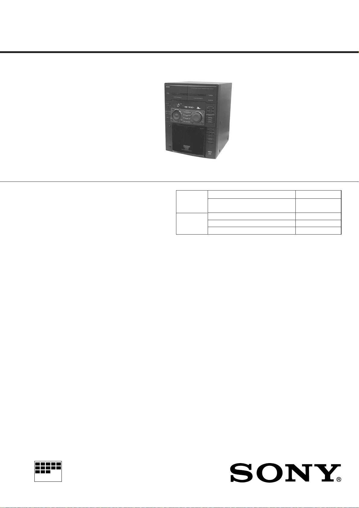
HCD-F50/F100/FR1
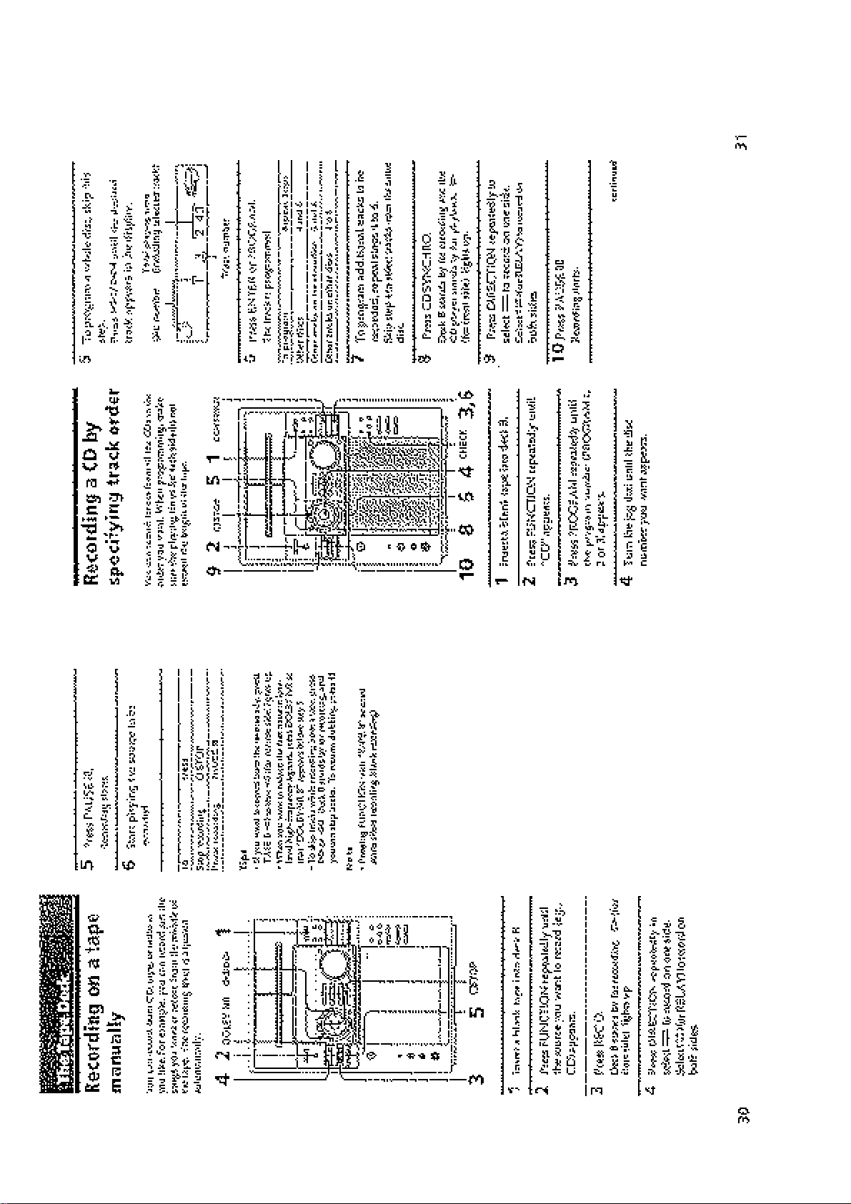
SERVICE MANUAL
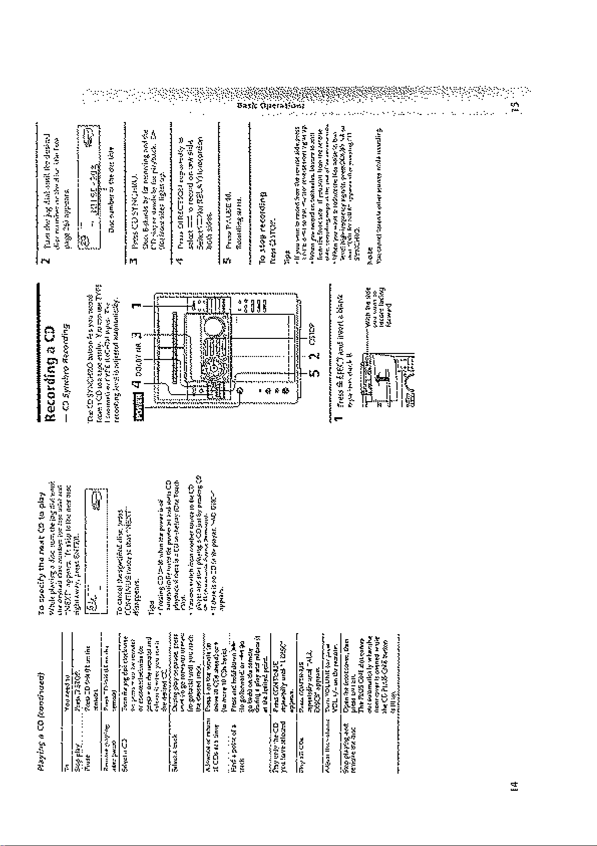
HCD-F50/F100/FR1 is the tuner, deck,
CD and amplifier section in MHC-F50/
F100/FR1.
Photo: HCD-FR1
US Model
Canadian Model
HCD-F50/F100
AEP Model
UK Model
E Model
Australian Model
HCD-FR1
* Dolby noise reduction manufacrured
under license from Dolby Laboratories
Licensing corporation.
"DOLBY" and the double-D symbol a
are trademarks of Dolby Laboratories
Licensing Corporation.
For the US model
AUDIO POWER SPECIFICATIONS
POWER OUTPUT AND TOTAL
HARMONIC DISTORTION:
With 8 ohm loads, both channels driven, from
70-20,000 Hz; rated 100 watts per channel
minimum RMS power, with no more than
0.9% total harmonic distortion from 250
milliwatts to rated output.
Amplifier section
Continuous RMS power output
Canadian model
100+100 watts
(8 ohms at 1 kHz, 5% THD)
(F100)
60+60 watts
(6 ohms at 1 kHz, 5% THD)
(F50)
Other models 100+100 watts
(8 ohm at 1 kHz, 10% THD)
Peak music power output (EXCEPT US, Canadian) :
1400 watts
CD
Section
Tape deck
Section
Model Name Using Similar Mechanism NEW
CD Mechanism Type
Optical Pick-up Name
Model Name Using
Tape Transport Mechanism Type TCM-220WR2
SPECIFICATIONS
Inputs VIDEO/MD IN (phono jacks) :
Outputs VIDEO/MD OUT (phono jacks)
voltage 250 mV,impedance 47
kilohms
MIX MIC (phone jack)
(Singapore model):
sensitivity 1 mV,
impedance 10 kilohms
: voltage 250 mV impedance
1 kilohms
PHONES (stereo phone jack) :
accepts headphones of 8 ohms or
more.
SPEAKER : accepts impedance of
8 to 16 ohms (F100/FR1)
accepts impedance of 6 to 16 ohms
(F50)
SURROUND SPEAKER
(F100/FR1):
accepts impedance of 16 ohms.
SUPER WOOFER (F100/FR1):
V oltage 1 V, impedance 1 kilo ohm
CDM-46B1 (F100/FR1)
CDM-46B2 (F50)
KSS-213B/S-N
Similar Mechanism HCD-D690/XB6
CD player section
System Compact disc and digital audio
system
Laser Semiconductor laser
(λ=780nm)
Emission duration: continuous
Laser output Max. 44.6 µW*
*This output is the value measured at a distance of 200 mm
from the objective lens surface
-on the Optical Pick-up Block
with 7 mm aperture.
Wavelength 780-790 nm
CD OPTICAL DIGITAL OUT
(Square optical connector jack, rear panel)
Wavelength 600 nm
– Continued on next page –
MICROFILM
MINI HI-FI COMPONENT SYSTEM
Tape player section
Recording system 4-track 2-channel stereo
Frequency response 60 - 13,000 Hz (±3 dB), using Sony TYPE I cassette
(DOLBY NR OFF) 60 - 14,000 Hz (±3 dB), using Sony TYPE II cassette
Tuner section
FM stereo, FM/AM superheterodyne tuner
FM tuner section
Tuning range 87.5 - 108,0 MHz
Antenna terminals 75 ohm unbalanced
Intermediate frequency 10.7 MHz
AM tuner section
Tuning range
North American model:
530 - 1,710 kHz
(with the AM tuning interval set at 10kHz)
531 - 1,710 kHz
(with the AM tuning interval set at 9 kHz)
Singaporian model: MW 531 - 1,602 kHz
(with the MW tuning interval set at 9 kHz)
530 - 1,710 kHz
(with the MW tuning interval set at 10 kHz)
SW 5.95 - 17.90 MHz
(with the SW tuning interval set at 5 kHz)
Other models:
531 - 1,602 kHz
(with the AM tuning interval set at 9 kHz)
530 - 1,710 kHz
(with the AM tuning interval set at 10 kHz)
Intermediate frequency 450 kHz
Antenna AM loop antenna
External antenna terminal
General
Power requirements
North American model: 120 V AC, 60 Hz
Australian model: 220 - 240 V AC, 50/60 Hz
AEP, UK, G models: 220 - 230V AC, 50/60 Hz
Other models: 110 - 120 V or 220 - 240 V AC,
50/60 Hz Adjustable with voltage selector
Power consumption
U.S. model: 195 watts (HCD-F100)
110 watts (HCD-F50)
Canadian model: 195 watts (HCD-F100)
120 watts (HCD-F50)
Other models: 210 watts
Dimensions (w/h/d) Approx. 280×375×450 mm
Mass Approx. 11.5 kg (HCD-F100/FR1)
Approx. 10 kg (HCD-F50)
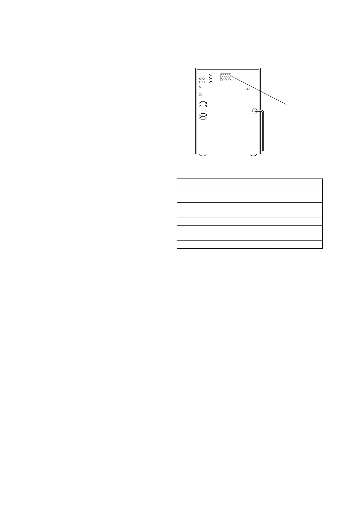
MEDEL IDENTIFICATION
– BACK PANEL –
PARTS No.
MODEL PARTS NO.
F50 : US model 4-990-400-0π
F50 : Canadeian model 4-990-400-1π
F100 : US model 4-990-364-0π
F100 : Canadian model 4-990-364-1π
FR1 : AEP, UK, German model 4-990-364-2π
FR1 : E model 4-990-364-5π
FR1 : Australian model 4-990-364-6π
FR1 : Singapore model 4-990-364-9π
Supplied accessories: AM loop antena (1)
Remote RM-SF100 (1) (F100/FR1)
Remote RM-SF50 (1) (F50)
Sony SUM-3 (N5)
batteries (2)
FM lead antenna (1)
Speaker coreds (2)
Design and specifications are subject to change without notice.
– 2 –
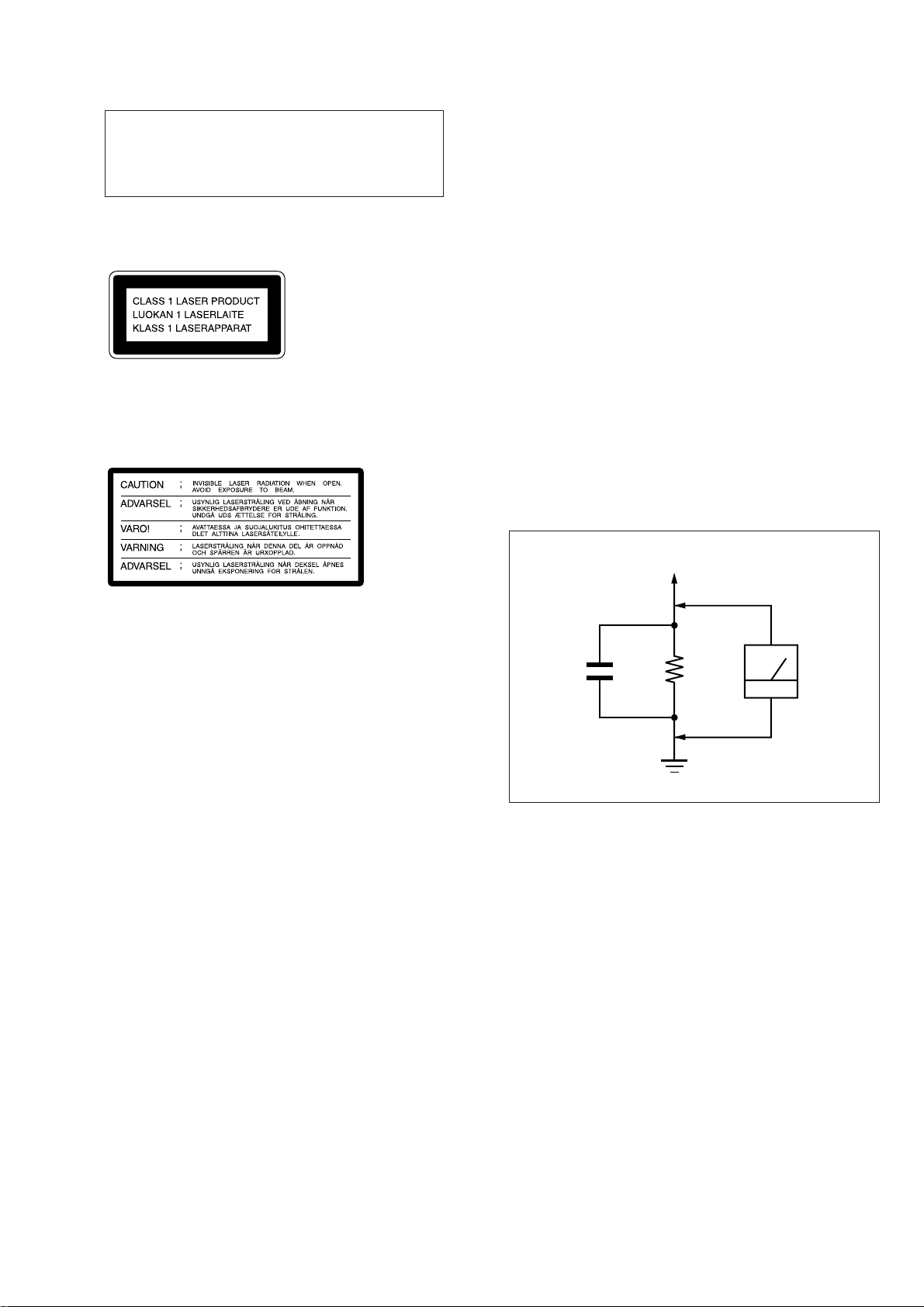
CAUTION
Use of controls or adjustments or performance of
procedures other than those specified herein may
result in hazardous radiation exposure.
This appliance is classified as a CLASS 1 LASER product.
The CLASS 1 LASER PRODUCT MARKING is located on
the rear exterior.
Laser component in this product is capable of emitting radiation
exceeding the limit for Class 1.
The following caution label is located inside the unit.
SAFETY CHECK-OUT
After correcting the original service problem, perform the following safety check before releasing the set to the customer:
Check the antenna terminals, metal trim, “metallized” knobs,
screws, and all other exposed metal parts for AC leakage.
Check leakage as described below.
LEAKAGE TEST
The AC leakage from any exposed metal part to earth ground and
from all exposed metal parts to any exposed metal part having a
return to chassis, must not exceed 0.5 mA (500 microampers.).
Leakage current can be measured by any one of three methods.
1. A commercial leakage tester, such as the Simpson 229 or RCA
WT -540A. Follow the manuf acturers’ instructions to use these
instruments.
2. A battery-operated AC milliammeter . The Data Precision 245
digital multimeter is suitable for this job.
3. Measuring the voltage drop across a resistor by means of a
VOM or battery-operated AC voltmeter. The “limit” indication is 0.75 V, so analog meters must have an accurate lowvoltage scale. The Simpson 250 and Sanwa SH-63Tr d are examples of a passive VOM that is suitable. Nearly all battery
operated digital multimeters that have a 2 V A C range are suitable. (See Fig. A)
To Exposed Metal
Parts on Set
SAFETY-RELATED COMPONENT WARNING!!
COMPONENTS IDENTIFIED BY MARK ! OR DOTTED
LINE WITH MARK ! ON THE SCHEMATIC DIA GRAMS
AND IN THE PARTS LIST ARE CRITICAL TO SAFE
OPERATION. REPLACE THESE COMPONENTS WITH
SONY PARTS WHOSE PART NUMBERS APPEAR AS
SHOWN IN THIS MANUAL OR IN SUPPLEMENTS PUBLISHED BY SONY.
AC
0.15 µF
1.5 k
Ω
Earth Ground
voltmeter
(0.75 V)
Fig. A. Using an AC voltmeter to check AC leakage.
ATTENTION AU COMPOSANT AYANT RAPPORT
À LA SÉCURITÉ!
LES COMPOSANTS IDENTIFIÉS P AR UNE MARQUE !
SUR LES DIAGRAMMES SCHÉMATIQUES ET LA LISTE
DES PIÈCES SONT CRITIQUES POUR LA SÉCURITÉ
DE FONCTIONNEMENT. NE REMPLACER CES COMPOSANTS QUE PAR DES PIÈCES SONY DONT LES
NUMÉROS SONT DONNÉS DANS CE MANUEL OU
DANS LES SUPPLÉMENTS PUBLIÉS PAR SONY.
– 3 –

TABLE OF CONTENTS
Servicing Notes ...........................................................................4
1. GENERAL ....................................................................5
2. DISASSEMBLY ......................................................... 25
3. TEST MODE ..............................................................33
4. MECHANICAL ADJUSTMENTS ........................36
5. ELECTRICAL ADJUSTMENTS
Deck Section.................................................................... 39
Tuner Section...................................................................41
CD Section.......................................................................42
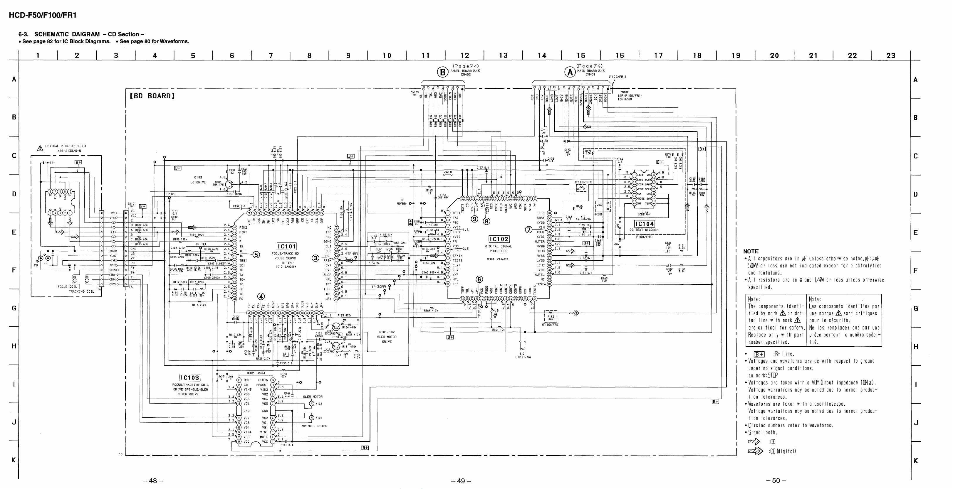
6. DIAGRAMS ................................................................44
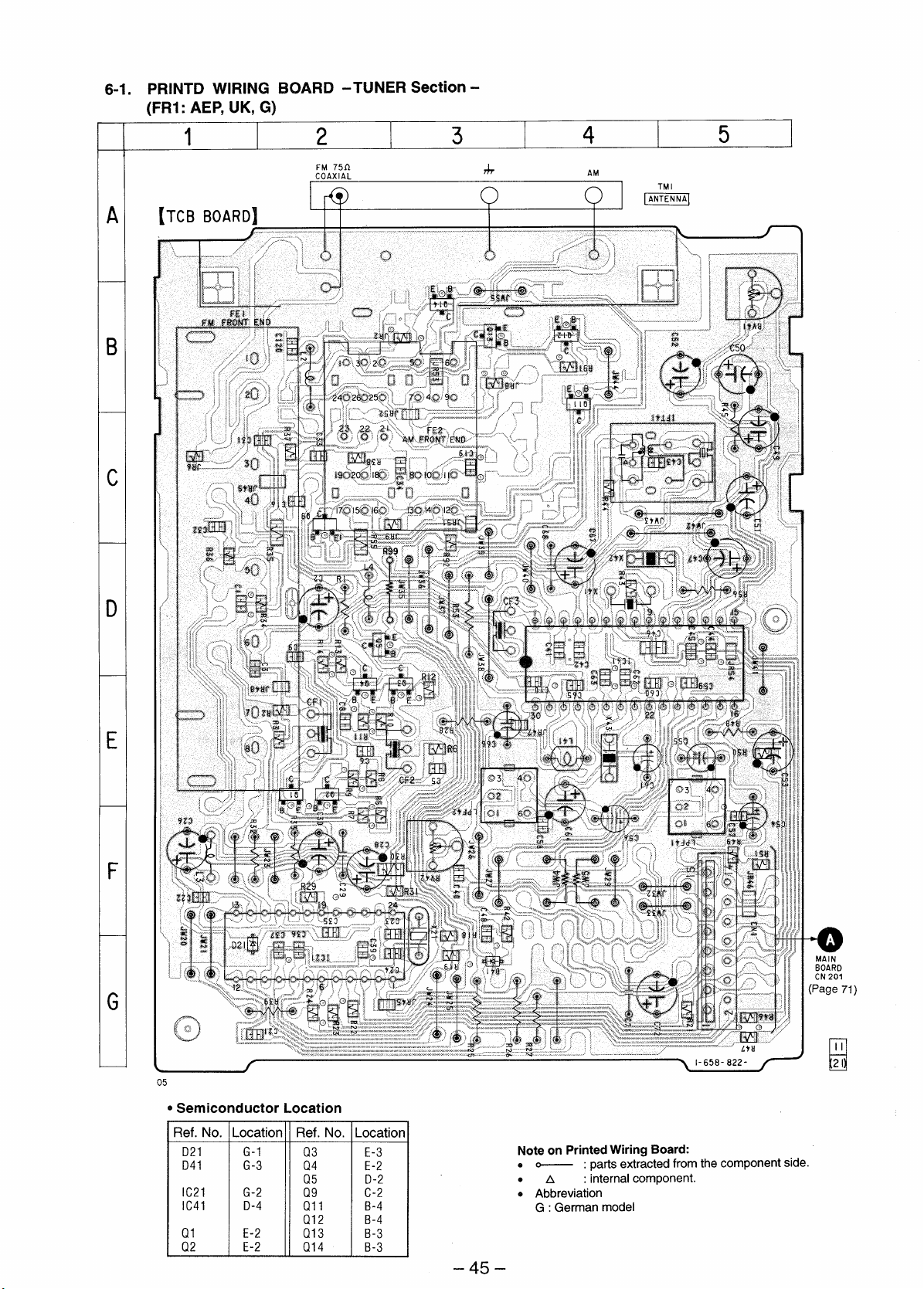
6-1. Printed Wiring Board –Tuner Section– ........................... 45
6-2. Schematic Diagram –Tuner Section– ..............................46
6-3. Schematic Diagram –CD Section– ..................................48
6-4. Printed Wiring Board –CD Section– ...............................51
6-5. Printed Wiring Boards –CD Motor Section–...................54
6-6. Schematic Diagram –CD Motor Section– .......................55
6-7. Printed Wiring Boards –Deck Section–........................... 57
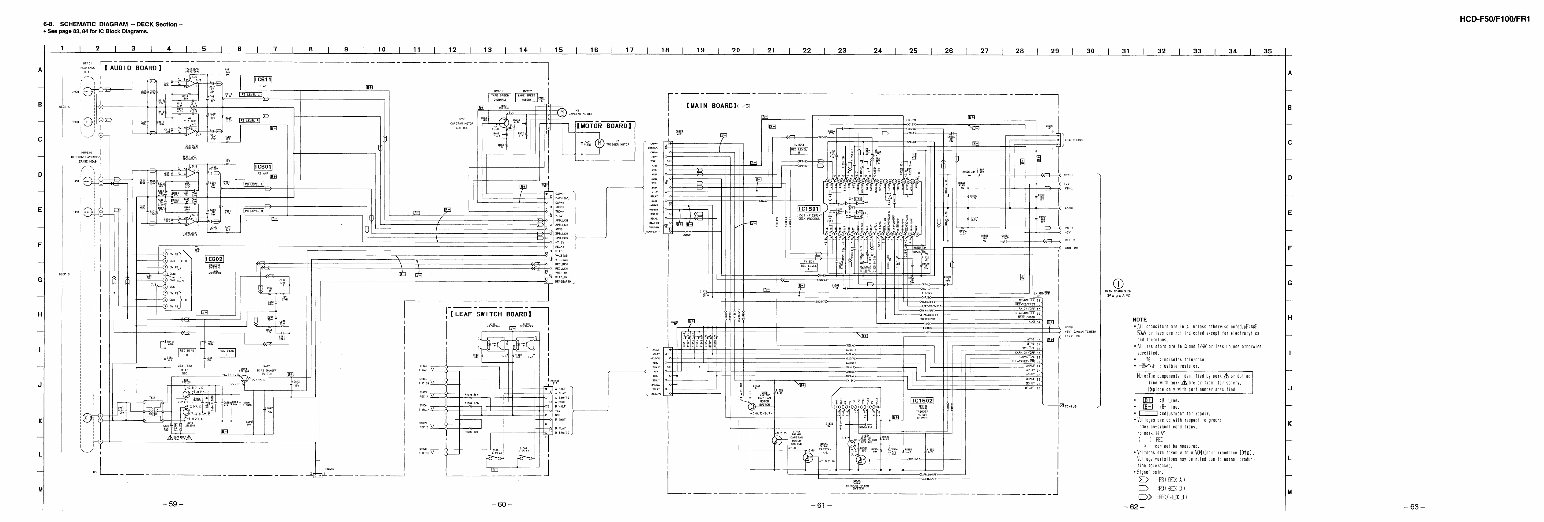
6-8. Schematic Diagram –Deck Section– ...............................59
6-9. Schematic Diagram –Main /Power Section–................... 64
6-10. Printed Wiring Boards –Main /Power Section– .............. 69
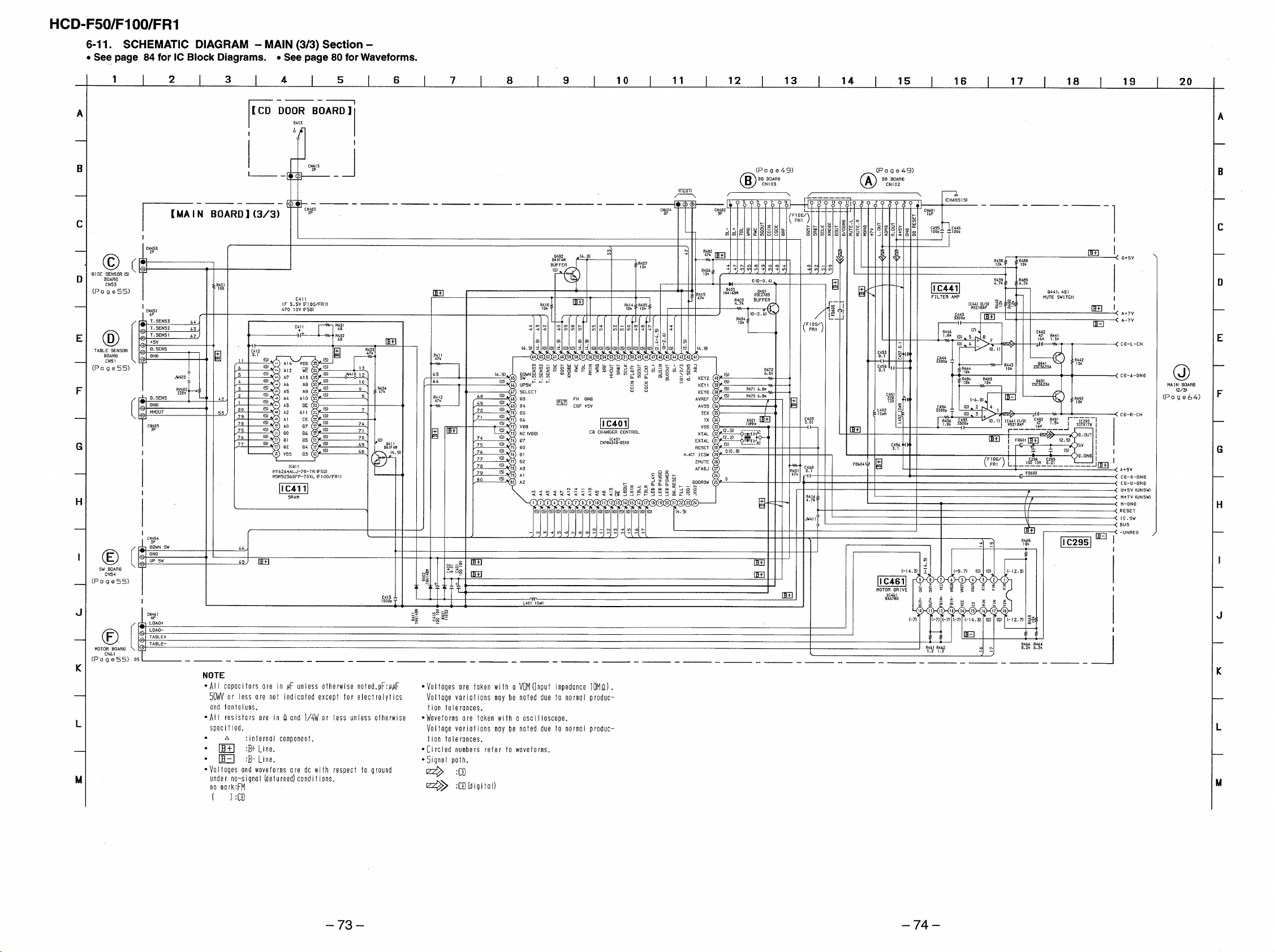
6-11. Schematic Diagram –Main (3/3) Section– ...................... 73
6-12. Printed Wiring Boards –Panel Section– ..........................75
6-13. Schematic Diagram –Panel Section–............................... 77
6-14. IC Pin Function Description ............................................85
7. EXPLODED- VIEWS ...............................................95
8. ELECTRICAL PARTS LIST ..............................104
SERVICING NOTES
NOTES ON HANDLING THE OPTICAL PICK-UP
BLOCK OR BASE UNIT
The laser diode in the optical pick-up block may suffer electrostatic break-down because of the potential difference generated
by the charged electrostatic load, etc. on clothing and the human
body.
During repair, pay attention to electrostatic break-down and also
use the procedure in the printed matter which is included in the
repair parts.
The flexible board is easily damaged and should be handled with
care.
NOTES ON LASER DIODE EMISSION CHECK
The laser beam on this model is concentrated so as to be focused
on the disc reflective surface by the objective lens in the optical
pick-up block. Therefore, when checking the laser diode emission,
observe from more than 30 cm away from the objective lens.
LASER DIODE AND FOCUS SEARCH OPERATION
CHECK
Carry out the “S curve check” in “CD section adjustment” and
check that the S curve waveform is output repeatedly.
Notes on chip component replacement
• Never reuse a disconnected chip component.
• Notice that the minus side of a tantalum capacitor may be dam-
aged by heat.
Flexible Circuit Board Repairing
• Keep the temperature of the soldering iron around 270 ˚C dur-
ing repairing.
• Do not touch the soldering iron on the same conductor of the
circuit board (within 3 times).
• Be careful not to apply force on the conductor when soldering
or unsoldering.
– 4 –
SECTION 1
GENERAL
This section is extracted
from instruction manual.
– 5 –
– 6 –
– 7 –
– 8 –
– 9 –
– 10 –
– 11 –
– 12 –
– 13 –
– 14 –
– 15 –
– 16 –
– 17 –
– 18 –
– 19 –
– 20 –

– 21 –
– 22 –
– 23 –
– 24 –
• This set can be disassembled in the order shown below.
SECTION 2
DISASSEMBLY
CASE
(Page 25)
FRONT PANEL
SECTION
(Page 26)
BACK PANEL
(Page 27)
SUB
CHASSIS
(Page 28)
TAPE MECHANISM
DECK SECTION
(Page 31)
DOOR ASS’Y
(Page 26)
MAIN BOARD
(Page 27)
CD MECHANISM
DECK SECTION
(Page 29)
• Abbreviation
G : German
SP : Singapore
AUS : Australian
Note: Follow the disassembly procedure in the numerical order given.
CASE
3
case
POWER TRANSFORMER (T901)
(Page 28)
AUDIO BOARD
(Page 31)
BASE
UNIT
(Page 29)
BD BOARD,
SLED MOTOR
(M102)
(Page 30)
CAPSTAN MOTOR (M1)
(Page 32)
2
three screws
(BVTP 3
OPTICAL
PICK-UP
(KSS-213B/S-N)
(Page 30)
×
8)
1
three screws
(CASE3 TP2)
1
three screws
(CASE3 TP2)
– 25 –
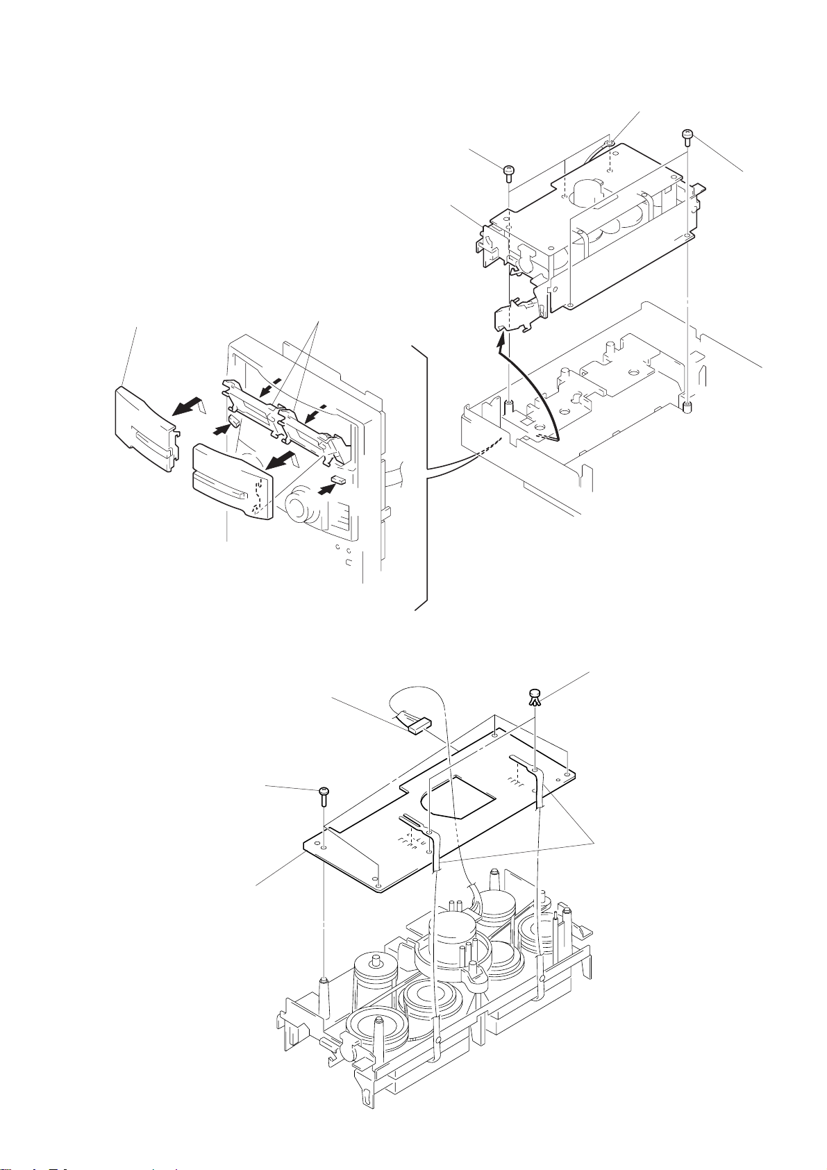
FRONT PANEL SECTION
1
wire (flat type) (21 core)
(CN601)
8
two claw
7
three screws
(BVTP 3
2
wire (flat type) (11 core)
(CN1001)
×
8)
5
screw (BVTT 3 × 8)
(FR1: AEP, UK, German)
8
two claw
6
lug
(FR1: AEP, UK, German)
4
connector
(CN403)
3
wire (flat type) (15 core) (EXCEPT FR1: SP)
wire (flat type) (19 core ) (FR1: SP)
(CN102)
DOOR ASS’Y
1
two screws
(PTPWH 2.6
×
6)
3
A
Remove the door ass’y
to direction of the
arrow
A
.
2
Open the door ass’y
– 26 –
BACK PANEL
1
wire (flat type) (13 core) (F50/F100/FR1: E, AUS)
wire (flat type) (15 core ) (FR1: AEP, UK, G, SP)
(CN1)
2
connector
(CN 105)
5
thirteen screws
(BVTP 3
6
Remove the back panel
to direction of the arrow.
×
4
8)
3
cover
five screws
(BVTP 3
×
8)
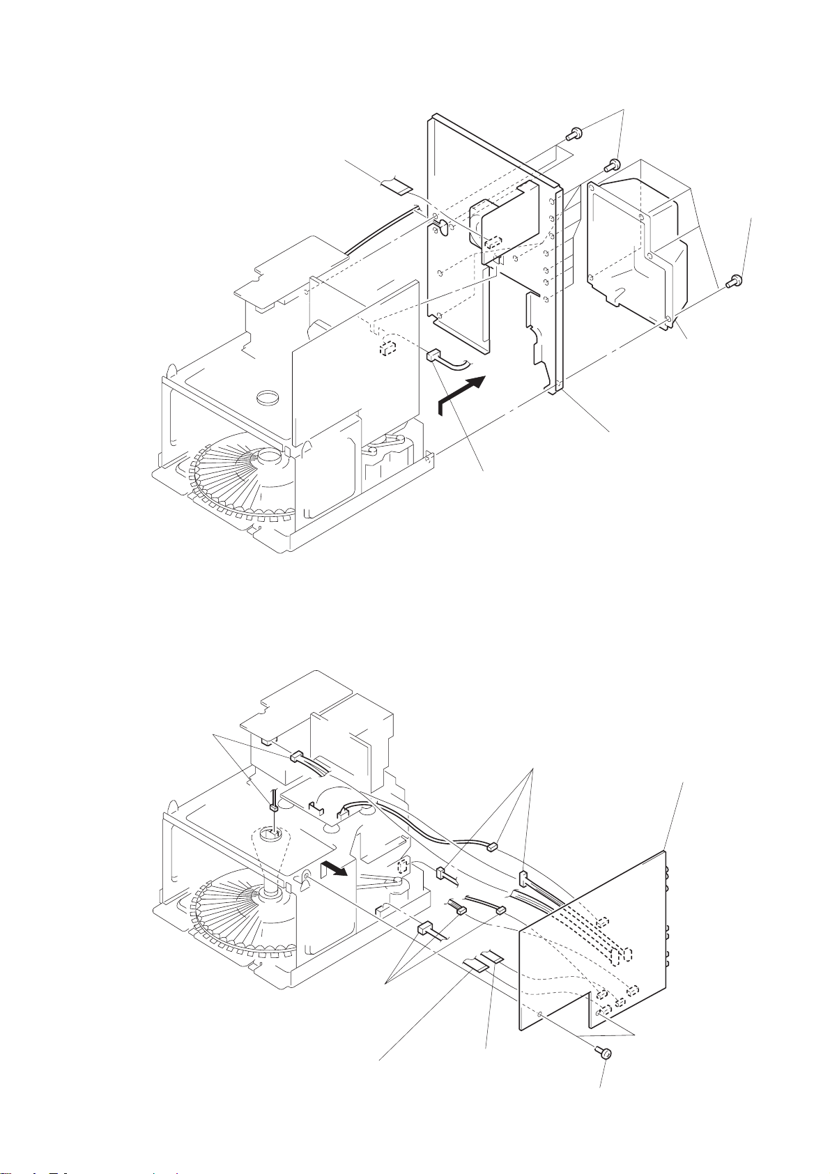
MAIN BOARD
3
two connectors
(CN901, 904)
3
threeconnectors
(CN61, 451, 453)
3
threeconnectors
(CN54, 202, 802)
5
Remove the MAIN
board to direction
of the arrow.
1
wire (flat type) (16 core)
(CN401)
2
wire (flat type) (9 core)
(CN402)
– 27 –
4
two screws
(BVTP 3
×
8)
POWER TRANSFORMER (T901)
4
power transformer
(T901)
3
four screws
(BVTT 3
1
×
8)
connector
(CN903)
2
power cord
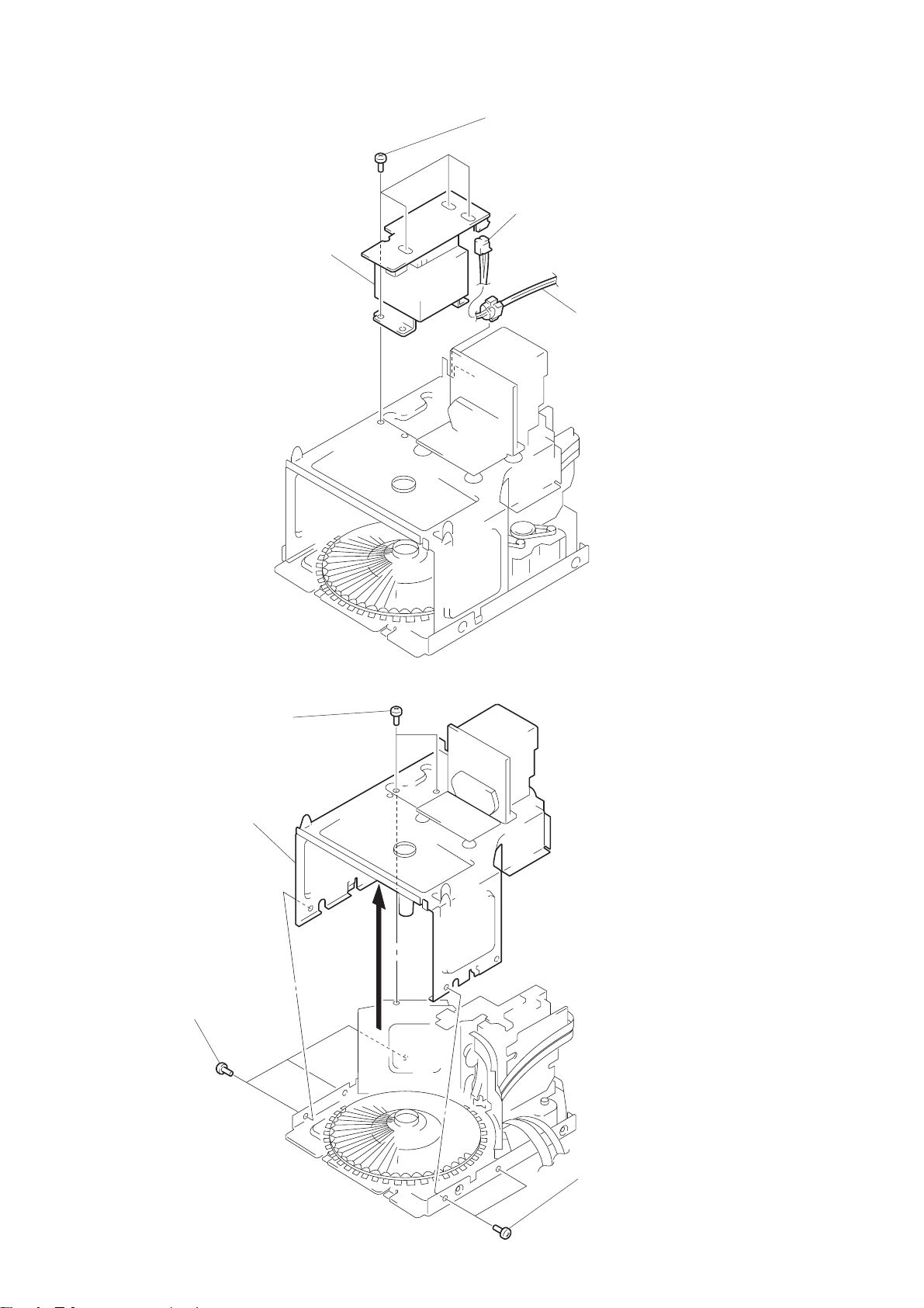
SUB CHASSIS
2
1
3
sub chassis
three screws
(BVTP 3
×
8)
two screws
(BVTT 3
×
8)
– 28 –
2
two screws
(BVTP 3
×
8)
CD MECHANISM DECK SECTION
5
two screws
7
1
screw
(PTPWH 2.6
reinforcement
×
8)
(BVTT 3
×
6)
!º
screw
(BVTP 3
6
wire holder
×
14)
!¡
screw
(BVTT 3
8
three screws
(BVTT 3
×
10)
×
10)
9
base (LOADING)
3
two screws
(BVTP 3
!™
base (CDM)
×
8)
2
table (S0)
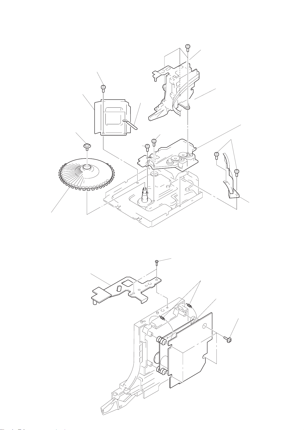
BASE UNIT
2
bracket
1
two screws
(BTP 2.6
×
8)
3
two tention springs
5
base unit
4
4
four screws
(PTPWH 2.6
cover (CD)
×
8)
– 29 –
BD BOARD, SLED MOTOR (M102)
6
gear (A) (S)
!º
two screws
(2
×
3)
!¡
sled motor
(M102)
5
claw
8
gear cover
7
three claws
9
gear (B) (RP)
1
wire (flat type) (16 core)
(CN101)
4
BD board
OPTICAL PICK-UP (KSS-213B/S-N)
3
Remove the optical
pick-up to direction
of the arrow
3
Removal
four solders.
A
.
A
2
screw
(B 2
×
5)
sled shaft
2
– 30 –
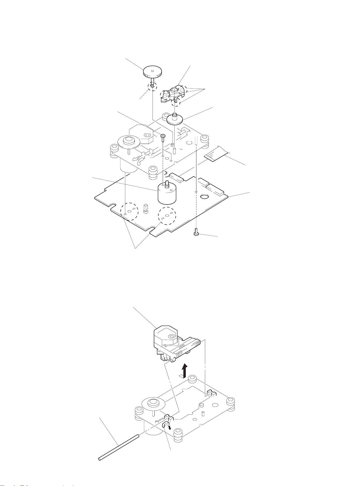
1
claw
TAPE MECHANISM DECK SECTION
Open two c assette
2
Remove the cassette lid (L) ass’y
to direction of the arrow
B
B
.
1
holders.
A
3
three screws
(BVTP 2.6
Remove the tape mechanism
5
deck section to direction of
the arrow
C
×
8)
.
C
4
lug
3
two screws
(BVTP 2.6
×
8)
2
Remove the cassette lid (R) ass’y
to direction of the arrow
AUDIO BOARD
4
four screws
(BTP 2.6
5
AUDIO board
A
.
2
1
connector
(CN651)
×
4)
two rivets
3
Break the soldering of two
flexible flat cables.
– 31 –

CAPSTAN MOTOR (M1)
4
1
Break the soldering of
motor lead.
Removal the capstan motor
to direction of the arrow.
3
claw
2
two screws
(BTP 2.6
×
8)
5
Hang the
two belts.
– 32 –

SECTION 3
TEST MODE
[MC Cold Reset]
• The cold reset clears all data including preset data stored in
the RAM to initial conditions. Execute this mode when returning the set to the customer.
Procedure:
1. Press three buttons FUNCTION , ENTER and CD PLUS 1
simultaneously.
2. The fluorescent indicator tube becomes blank instantaneously ,
and the set is reset.
[MC Hot Reset]
• This mode resets the set with the preset data kept stored in the
memory. The hot reset mode functions same as if the power
cord is plugged in and out.
Procedure:
1. Press three buttons FUNCTION , ENTER and
CONTINUE/TUNING MODE simultaneously.
2. The fluorescent indicator tube becomes blank instantaneously ,
and the set is reset.
[MC Test Mode]
• This mode can be used for operation check of Ampsection,
Tuner section and Deck section.
Procedure:
• Press three buttons FUNTION , ENTER
and PROGRAM simultaneously.
In the MC Test Mode, blinking the fluorescent indicator tube
displays “Volume”.
1. Test Mode in Amp Section
• Press GEQ MEMO button to GEG maximum and SUR
off.
• Press EFFECT button to GEQ flat and SUR off.
• Press GEQ FILE button to GEQ minimum and SUR off.
• Rotarion VOLUME knob in “+” derection a little, the
fuorescent indicator tube displays “Volume MAX”.
• Rotation VOLUME knob in “–” direction a little, the
fluorescent indicator tube displays “Volume MIN”.
• Other function is a regular.
2. Test Mode in Tuner Section
• In the preset mode
• If after cold reset, preset value set a master control I.C.
• Receive tuning UP/DN sircs irrepective of during
testmode.
3. Test Mode in Deck Section
• If recording, function to Video and line mute off.
• Rewind after recording the tape stop to begin the recording
point.
• If press HI-SPEED DUBBING button during recoeding,
exactly the tape speed fast.
• If press HI-SPEED DUBIING button during playback,
the tape speed fast. One more press button, back to a
normal.
[Change-over of FUNCTION Name]
• The FUNCTION name of external input terminal can be
changed over to VIDEO or MD.
Procedure:
1. Press POWER button to turn the set OFF.
2. Press POWER button together with GROOVE button, and
the power is turned on, the display of fluorescent indicator
tube changes to “MD” or “VIDEO” instantaneously, and thus
the FUNCTION is changed over.
[Change-over of AM T uner Step between 9kHz and 10kHz]
• A step of AM channels can be changed over between 9kHz
and 10kHz.
Procedure:
1. Press POWER button to turn the set ON.
2. Select the function “TUNER”, and press TUNER/BAND
button to select the BAND “AM”.
3. Press POWER button to turn the set OFF.
4. Press ENTER and POWER buttons simultaneously , and the
display of fluorescent indicator tube changes to “AM 9k STEP”
or “AM 10k STEP”, and thus the c hannel step is changed over .
[LED and Fluorescent Indicator Tube All Lit, Key Check
Mode]
Procedure:
1. Press three buttons FUNCTION ,
ENTER and SHUFFLE simultaneously.
2. LEDs and fluorescent indicator tube are all turned on.
Press CD PLUS 1 button, the fluorescent indicator tube displays MC version, GC version, model name and destination to
cycle.
3. Press CONTINUE button, and the key check mode is activated.
4. In the key check mode, the fluorescent indicator tube displays
“K 1 V0 J0”. Each time a button is pressed, “K”value increases. However , once a button is pressed, it is no longer taken
into account.
“J” value increases like 1, 2, 3 ... if rotating JOG knob in “+”
direction, or it decreases like 0, 9, 8 ... if rotating in “–” direction.
“V” value increases like 1, 2, 3 ... if rotating VOLUME knob
in “+” direction, or it decreases like 0, 9, 8 ... if rotating in “–
” direction.
5. To exit from this mode, press three buttons in the same manner a step 1, or disconnect the power cord.
[ADJ MODE]
Procedure:
1. Press the POWER button to turn the power ON.
2. Open the front cover, and press the PLUS ONE button.
3. Set the disc (YEDS-18 : 3-702-101-01) in the PLUS ONE slit.
4. Close the front cover, and chuck the disc.
5. Press the POWER button, and turn OFF the power.
6. Connect TP (TP301:ADJ) of the DISPLAY board and the
ground with a lead wire.
7. Press the POWER button and turn ON the power.
The ADJ mode is set with the above.
Differences with normal mode
• No high speed search is performed during access
• Ignored even if GFS becomes L
• Ignored even if Q data cannot be read
• Spindle servo gain is set to 12 cm mode (Even with 8 cm disc)
The following special functions will work when certain functions
are pressed in this mode.
Special functions in ADJ mode
(The ( ) buttons function only with the general purpose remote.)
Button Function
(3)
(8)
CHECK
CLEAR
Tracking servo, sled servo OFF
Tracking servo, sled servo ON
S shape observation mode
Eccentric measurement mode
– 33 –

[Aging Mode]
• This mode can be used for operation check of CD section and
tape deck section.
• If an error occurred:
The aging operation stops.
• If no error occurs:
The aging operation continues repeatedly.
1. Aging Mode in CD Section
• Operating jig (HCD-F50 only)
Remote Commander (for aging mode): J-2501-123-A
1-1. Operating Method of Aging Mode
1. Turn ON the power of the unit. Open the front cover.
2. Press three buttons ENTER , FUNCTION and
MEMO INPUT simultaneously .
3. When the disc set mode is set, the ( and P LEDs blink.
4. Rotate the JOG dial. The slits (No. 10, 20, 30, 40, 51) for set-
ting the discs will come forward. Insert the discs into these
slits. Do not set the discs in other slits.
5. Set the use/disuse of the self protection function in errors. Press
the REPEA T b utton. When REPEAT is displayed on the fluorescent indicator tube, the self protection function during the
error will become “Use”.
If the REPEAT display is OFF, it means that the function is
not used. (Normally set to “Use” when performing aging.)
7. Cloase the front cover and press the ^ button.
8. The ( LED will light up, the aging mode is set, and aging
is started.
9. The aging cycle lasts 3 minutes. When problems occur during
aging, the error number will be displayed on the fluorescent
indicator tube, ( LED blinks, and the P LED will
light up.
(Refer to the following table for the details of the errors.)
10. Aging will be repeated as long as no errors occur.
11. After each aging cycle, the number displayed on the Fluores-
cent indicator tube will increase.
12. To end aging, press the POWER button
1-2. CD Section Sequence
• During the aging mode, compact disces are seleted in the fol-
lowing sequence:
Sequence of Aging Mode
Order of Disc Chenge
(1 sycle takes 3 minutes)
Disc change
No.51
Load in
No.20
TOC read
No.40
Access of last track
No.30
3 second playback
No.10
Access of first track
No.40*
3 second playback
Load out
* DISC No.40 chucks twice during one cycle.
To differentiate, the “PROGRAM” indicator of the fluorescent indicator tube will light up during the second chucking.
Error Display
DISC
51
Disc number
number of agings
0C
Err
26
Error code
Error code
Code number
Err 01
Err 02
Err 03
Err 04
Err 05
Err 06
Err *1
Err *2
Err *3
Err *4
Err *5
Err *6
DISC sensor check 1
DISC sensor check 2
Table operation check 2
Loading operation check 1
Loading operation check 2
BU related check 1
BU related check 2
BU related check 3
BU related check 4
BU related check 5
BU related check 6
Name
No disc in the specified slit
Disc in other slits
No function
No table sensor input
Load in timeover
Load out timeover
Access timeover
High speed search NG
Q data read error
BU operation (From focus search to until signal can be read) timeover
GFS monitor error
Focus cannot be imposed by focus search
The * numbers mean the following according to the state of the unit during aging
2 : From chucking to end of TOC read
3 : From end of TOC read to end of last track playback
4 : From end of last track playback to end of first track playback
Contents
– 34 –

2. Aging Mode in Tape Deck Section (HCD-F100/FR1
only)
2-1. Operating Method of Aging Mode
1. Load a commercially available 10-minute tape into the decks
A and B respectively.
(If a 10-minute tape is not available, another tape may be used
but a cycle time will be longer.)
2. Select the function “TAPE”.
3. Rewind tapes in advance by pressing 0 button respectively
on decks A and B.
4. Press three buttons ENTER , FUNCTION , and
MEMO INPUT simultaneously.
5. Press TAPE A ( button. (This button triggers the aging
mode.)
6. The aging mode is activated if “AGING A” is displayed on
the fluorescent indicator tube.
7. In the aging mode, the aging is executed in a sequence given
in “2-2. Operation during Aging Mode”.
The aging continues unless an alarm occurred.
8. To exit from the aging mode, press POWER button to turn
the set OFF.
2-2. Operation during Aging Mode
In the aging mode, the program is executed in the following
sequence.
1. A tape on FWD side is played for one minute.
2. PAUSE STOP is made.
3. Recording is made for 3 minutes. (For the deck not having the
record function, the play is executed. In this case, ( LED
does not light up.)
4. FF is executed up to the end of tape.
5. A tape is reversed, and the tape on REV side is played for one
minute.
6. PAUSE STOP is made.
7. Recording is made for 3 minutes. (For the deck not having the
record function, the play is executed. In this case, 9 LED
does not light up.)
8. FF is executed up to the end of tape.
9. Steps 1 through 8 are executed for the other deck.
10. Steps 1 through 9 are repeated unless an alarm occurred.
Location:
[MAIN BOARD] (Component Side)
CN401
CN402
1 2 3
CN404
IC461
2-3. Deck Section Sequence
• During the aging mode, decks are selected in the following
sequence:
Deck A (FWD) → Deck A (REV)
↑ ↓
Deck B (REV) ← Deck B (FWD)
– 35 –

SECTION 4
MECHANICAL ADJUSTMENT
• TAPE MECHANISM DECK SECTION
PRECAUTION
1. Clean the following parts with a denatured-alcohol-moistened
swab:
• Tor que Measurement
Torque Torque Meter Meter Reading
Forward CQ-102C
record/playback head pinch roller
erase head rubber belts
capstan idlers
Forward
Back Tension (0.026 – 0.082 oz•inch)
2. Demagnetize the record/playback head with a head demagnetizer.
Reverse CQ-102RC
3. Do not use a magnetized screwdriver for the adjustments.
4. After the adjustments, apply suitable locking compound to the
parts adjusted.
5. The adjustments should be performed with the rated power
supply voltage unless otherwise noted.
Reverse
Back Tension (0.026 – 0.082 oz•inch)
FF, REW CQ-201B
• Tape Tension Measurement
Torque Tension Meter Meter Reading
Forward CQ-403A more than 100 g (3.52 oz)
Reverse CQ-403R more than 100 g (3.52 oz)
• CD MECHANISM DECK SECTION
To adjust the mechanism section, enter the mechanism section adjustment mode.
For how to enter the mechanism section adjustment mode, refer to each adjustment section.
CQ-102C
CQ-102RC
36 to 61g•cm
(0.50 – 0.84 oz•inch)
2 to 6g•cm
36 to 61g•cm
(0.50 – 0.84 oz•inch)
2 to 6g•cm
61 to 143g•cm
(0.85 – 1.98 oz•inch)
DISC SENSOR ALIGMENT
1. Make sure that there is no disc in the unit.
2. Connect an oscilloscope to CN405 of the MAIN board.
oscilloscope
D SENS
GND
HH OUT
MAIN board
CN405
3. While pressing the CLEAR and CD PLUS 1 buttons at the same time and turn ON the power.
0 =
POWER button
button
SENS (CH1)
TEST (CH2)
GND
) +
CD PLUS 1 button
button
– 36 –
CLEAR button
CHECK button

4. The fluorescent indicator tube shows as follows, and the mechanism section adjustment mode is set.
PLUS ONE
5. The disc table rotates in the counterclockwise direction. The disc table rotation time is displayed with ‘’PLUS ONE” slit as a measuring
point. (“LEFt” is displayed initially.)
6. Measure the waveform of the oscilloscope when the disc table is rotating.
7. Move the holder (sensor) center so that the flat portion center at the top of the SENS (CH1) input waveform and the ‘’H” center of TEST
(CH2) coincide.
Holder (sensor)
TEST (CH2) waveform
SENS (CH1) waveform
Fixed screw
Flat portion center of
SENS (CH1) waveform
8. Tighten the fixed screw to fix the disc table, then press the CLEAR button.
9. The disc table rotates in the clockwise direction. Measure the waveform and make sure that the flat portion center at the top of the SENS
(CH1) input waveform and the ‘’H” center of TEST (CH2) coincide.
10. If the adjustment is not successful, press the CLEAR button to rotate the disc table in the counterclockwise direction, and perform steps
6 to 9.
Note:During the adjustment mode, the rotational direction is switched each time the CLEAR button is pressed. Immediately after the
button is pressed, “LEFt” or “rght” is displayed to notify of the rotational direction.
Pressing the CHECK button enters the loading mode which will be described later . Pressing the CLEAR button rotates the disc table
again.
– 37 –

MAGNET ASSY ALIGMENT
1. Check that there is no disc in the unit and then turn ON the power. Open the door, and set a disc in the PLUS ONE slit.
2. Turn OFF the power, close the door , and w hile pressing the CLEAR and CD PLUS 1 buttons simultaneously, turn ON the power ag ain.
3. Press the CHECK button, and set the loading mode.
4. Press the ) + button and chuck the disc.
5. Adjust the magnet assembly and magnet holder so that A=B as shown in the figure.
AB
Magnet ASSY
Magnet holder
Magnet ASSY
Screw (For adjustment)
DISC HOLDER A ALIGMENT
1. Check that there is no disc in the unit and then turn ON the power. Open the door, and set a disc in the PLUS ONE slit.
2. Turn OFF the power, close the door , and w hile pressing the CLEAR and CD PLUS 1 buttons simultaneously, turn ON the power ag ain.
3. Press the CHECK button, and set the loading mode.
4. Press the ) + button and chuck the disc.
5. Press ) + or 0 = button to stop the disc holder A slightly away from the disc.
6. Rotate and adjust the adjusting screw so that the center of the disc and that of the disc holder coincide.
Disc
Disc holder A
a
a = b
Disc holder A
Disc
b
Screw (For adjustment)
– 38 –
SECTION 5
main
board
CN207
set
test tape
P-4-A100
(10kHz, –10dB)
pin
3
oscilloscope
L-CH
R-CH
V
H
waveform of oscilloscope
in phase 45°90°135°180
°
good
wrong
pin
2
pin
1
L
R
reverse
forward
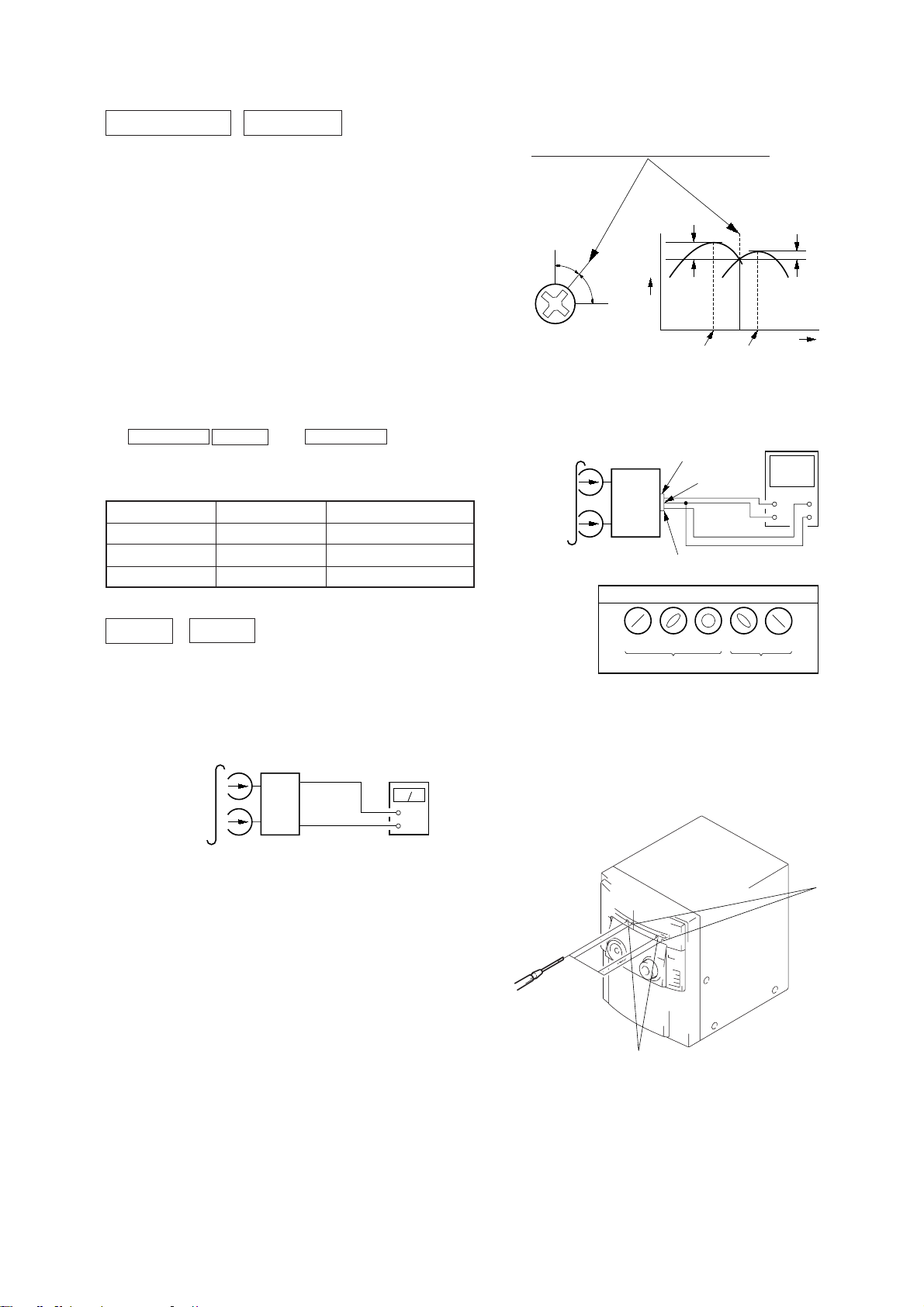
ELECTRICAL ADJUSTMENTS
DECK SECTION 0dB=0.775V
1. Demagnetize the record/playback head with a head demagne-
tizer. (Do not bring the head demagnetizer close to the erase
head.)
2. Do not use a magnetized screwdriver for the adjustments.
3. After the adjustments, apply suitable locking compound to the
parts adjust.
4. The adjustments should be performed with the rated power
supply voltage unless otherwise noted.
5. The adjustments should be performed in the order given in
this service manual. (As a general rule, playback circuit adjustment should be completed before performing recording
circuit adjustment.)
6. The adjustments should be performed for both L-CH and R-
ch.
7. Switches and controls should be set as follows unless other-
wise specified.
8. Set to test mode. (Press key switch same time
FUNCTION ENTER and PROGRAM button.)
• Test Tape
Tape Signal Used for
P-4-A100 10kHz, –10 dB Azimuth Adjustment
WS-48B 3kHz, 0dB Tape Speed Adjustment
P-4-L300 315Hz 0dB Level Adjustment
2. Turn the adjustment screw and check output peaks. If the peaks
do not match for L-CH and R-CH, turn the adjustment screw
so that outputs match within 1dB of peak.
output
level
within
1dB
L-CH
peak
R-CH
peak
within
1dB
Screw
position
L-CH
peak
Screw
position
R-CH
peak
3. Mode: Playback (FWD)
Record/Playback Head Azimuth Adjustment
DECK A DECK B
Note: Perform this adjustments for both decks
Procedure:
1. Mode: Playback (FWD)
test tape
P-4-A100
(10KHz, –10dB)
set
main board
CN207
Pin
1
(L-CH)
Pin
3
(R-CH)
main board
CN207
2
Pin
level meter
+
–
4. Repeat steps 1 to 3 in playback (REV) mode.
5. After the adjustments, apply suitable locking compound to the
pats adjusted.
Adjustment Location: Record/Playback Head (Deck A and B)
and MAIN board.
– 39 –

Tape Speed Adjustment DECK A
Note: Start the Tape Speed adjustment as below after setting to
the test mode.
In the test mode, the tape speed is high during pressing the
HIGH SPEED DUBBING button.
Procedure:
1. Turn the power switch on.
2. Press the FUNCTION button, ENTER button and
PROGRAM button simultaneously.
To exit from the test mode, press the POWER button.
Mode: Playback (FWD)
1. Insert the WS-48B into the deck A and the blank tape into the
test tape
WS-48B
(3 kHz, 0 dB)
set
main board
CN207 (Pin
(Pin 3 :R-CH)
frequency counter
+
–
1
: L-CH)
deck B.
2. Press the REC button and ( button on the deck B. Then
the deck B is at recording mode.
3. Set the deck A to playback mode.
4. Keep pressing the HIGH SPEED DUBBING button in play-
back mode.
Then at HIGH speed mode.
5. Adjust R V652 on the AUDIO board do that frequency counter
reads 6,000 ± 90 Hz.
6. Take off the HIGH SPEED DUBBING button.
Then at NORMAL speed mode.
7. Adjust R V651 on the A UDIO board so that frequenc y counter
reads 3,000 ± 90 Hz.
8. Frequency difference between deck A and deck B the begin-
ning of the tape should be within ± 1.5 %.
Adjustment Location: AUDIO board
Sample Volue of Wow and Flutter: 0.3% or less W.RMS
(WS-48B)
Playback level Adjustment DECK A DECK B
Procedure:
Mode: Playback (FWD)
test tape
P-4-L300
(315 Hz, 0 dB)
set
main board
CN207 (Pin
(Pin
level meter
1
: L-CH)
3
: R-CH)
+
–
Deck A is RV311 (L-CH) and RV411 (R-CH), Deck B is RV301
(L-CH) and RV401 (R-CH) so that adjustment within adjustment
level as follows.
Adjustment Level:
CN207 PB level: 301.5 to 338.3 mV (–8.2 to –7.2 dB) level
difference between the channels: within ±0.5 dB
Adjustment Location: AUDIO and MAIN boards
Record bias Current Adjustment DECK B
Procedure:
1. Mode: record
Pin 6 (L-CH) of IC1501 on the main board.
Pin
#
(L-CH) of IC1501 on the main board.
1) 315 Hz
2) 10 kHz
AF OSC
attenuator
Pin 2 (GND) of ICN207 on the main board.
50 mV (–23.8 dB)
Ω
600
set
blank tape
CN-123
2. Mode: Playback
recorded
portion
set
CN207 (Pin
(Pin
level meter
1
: L-CH)
3
: R-CH)
+
–
Confirm playback the signal recorded in step 1 become adjustable
limits as follows.
If these levels do not adjustable limits, adjustment the R V341 (L-CH)
and RV441 (R-CH) on the AUDIO board to repeat steps 1 and 2.
Adjustable limits: Playback output of 315 Hz to playback output
of 10kHz: ±0.5 dB
Adjustment Location: AUDIO and MAIN boards
Record Level Adjustment DECK B
Procedure:
1. Mode: record
Pin
6
(L-CH) of IC1501 on the main board.
Pin
#
(R-CH) of IC1501 on the main board.
AF OSC
315 Hz, 50 mV (–23.8 dB)
Ω
attenuator
Pin
2
(GND) of CN207 on the main board.
600
blank tape
CS-123
set
2. Mode: Playback
recorded
portion
set
CN207 (Pin
(Pin
level meter
1
: L-CH)
3
: R-CH)
+
–
Confirm playback the signal recorded in step 1 become adjustable
limits as follows.
If these levels do not adjustable limits, adjustment the RV1501 (LCH) and RV1551 (R-CH) on the main boar d to repeat steps 1 and 2.
Adjustable limits:
CN207 PB level: 47.3 to 53.1 mV (–24.3 to –23.3 dB)
Adjustment Location: MAIN board
– 40 –
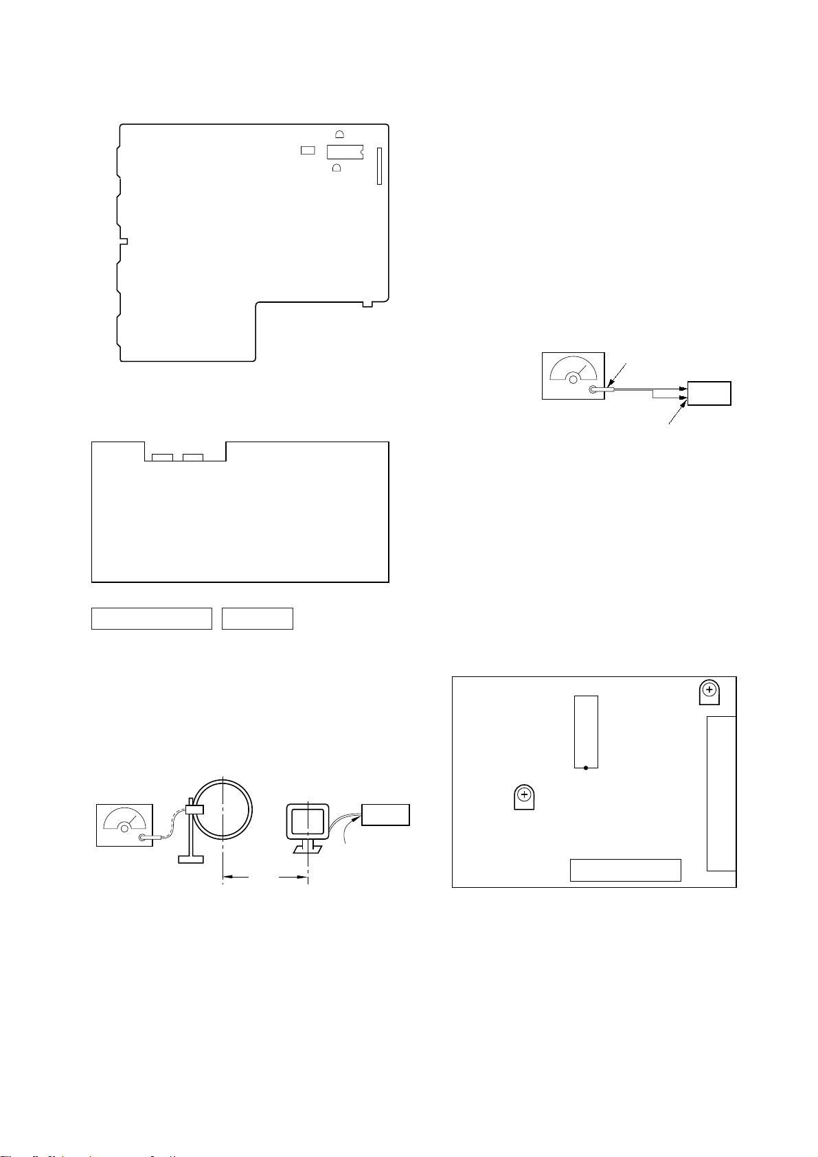
[MAIN BOARD] (Component Side)
CN207
RV1501
RV1551
IC1501
CN205
AM Tuned Level Adjustment
Band: AM or MW
Procedure:
1. Set the output of SSG so that the input level of the set becomes 55 dB.
2. Tune the set to 999 kHz.
3. Adjust R V41 to the point (moment) when the TUNED indicator will change from going off to going on.
Adjustment Location : TCB board
FM Section Adjustment
Note: This adjustment should be performed after the AM Tuned
Level Adjustment due to the same adjustment element.
Setting:
FM RF stereo signal
generator
75
Ω
coaxial
[AUDIO BOARD] (Conductor Side)
RV301
®
RV401
®
PB LEVEL
– DECK B –
RECORD
BAIS
R
L
RV441RV341
R
L
TAPE SPEED
(NORMAL)
RV651
®
PB
LEVEL
– DECK A –
(HIGH)
RV652
RV311
RV411
R
®
L
®
®
TUNER SECTION 0dB=1µV
(HCD-FR1: AEP, UK, German model only)
Note: As a front-end (FE1) is difficult to repair if faulty, replace
it with new one.
AM Section Adjustment
Setting:
loop antenna A
AM RF signal
generator
loop antenna B
set
set
Carrier frequency : 98 MHz
Modulation : AUDIO 1 kH, 75 kHz
deviation (100%)
FM ANTENNA terminal
(TM1) (75
Ω
open)
FM Tuned Level Adjustment
Band: FM
Procedure:
1. Supply a 25dBµ 98 MHz signal from the ANTENNA terminal.
2. Tune the set to 98 MHz.
3. If the TUNED indicator does not light, adjust RV42 to the
point (moment) when the TUNED indicator will change from
going off to going on.
Adjustment Location: TCB board
[TCB BOARD] (Component Side)
IC41
RV42
RV41
TM1
30% amplitude
modulation by
400 Hz signal
60 cm
AM ANTENNA
terminal (TM1)
FE1
– 41 –

CD SECTION
Note :
1. CD Block is basically designed to operate without adjustment.
Therefore, check each item in order given.
2. Use YEDS-18 disc (3-702-101-01) unless otherwise indicated.
3. Use an oscilloscope with more than 10MΩ impedance.
4. Clean the object lens by an applicator with neutral detergent when
the signal level is low than specified value with the following
checks.
oscilloscope
BD board
TP (FE)
TP (VC)
10. Confirm that oscilloscope waveform is clear and check RF signal level is correct or not.
11. Turn OFF the power, and remove the lead wire connected at
step 7.
Note : A clear RF signal waveform means that the shape “◊” can
be clearly distinguished at the center of the waveform.
RF signal waveform
VOLT/DIV : 200mV
TIME/DIV : 500ns
level : 1.8 ± Vp-p
+0.3
–0.2
S Curve Check
Procedure :
1. Press the POWER button to turn ON the power .
2. Open the front cover, and press the CD PLUS1 button.
3. Set the disc (YEDS-18) into the “PLUS ONE” slit.
4. Close the front cover, and chuck the disc.
5. Press the POWER button to turn OFF the power.
6. Connect the oscilloscope to TP (FE) of the BD board.
7. Connect CN404 pin 2 of the MAIN board and the ground
(CN404 pin 1 or 3) with a lead wire.
8. Press the POWER button to turn ON the power.
9. The first track will be played back automatically. When the
CHECK button is pressed, “S JI” will be displayed on the fluorescent indicator tube, and focus search will be repeated.
10. Check the oscilloscope waveform (S-curve) is symmetrical be-
tween A and B. And confirm peak to peak le vel within 1.8 ± 0.6
Vp-p.
S-curve waveform
symmetry
A
within 1.8 ± 0.6Vp-p
B
11. Turn OFF the power, and remove the lead wire connected at
step 7.
Note : • Try to measure several times to make sure than the ratio
of A : B or B : A is more than 10 : 7.
• Take sweep time as long as possible and light up the
brightness to obtain best waveform.
RF Level Check
oscilloscope
BD board
E-F Balance (Traverse) Check
The procedure for this checking method differs for when a general remote control unit is used and not used.
oscilloscope
BD board
TP (TE)
TP (VC)
When a general remote commander is used:
1. Press the POWER button to turn ON the power.
2. Open the front cover, and press the CD PLUS1 button.
3. Set the disc (YEDS-18) into the “PLUS ONE” slit.
4. Close the front cover, and chuck the disc.
5. Press the POWER button to turn OFF the power.
6. Connect the oscilloscope to TP (TE) of the BD board.
7. Connect CN404 pin 2 of the MAIN board and the ground
(CN404 pin 1 or 3) with a lead wire.
8. Press the POWER button to turn ON the power.
9. Playback the fifth track of the disc.
10. Press the 3 button on the remote commander. (The tracking
servo and the sledding servo are turned OFF.)
11. Check the level B of the oscilliscope's waveform and the A (DC
voltage) of the center of the Traverse waveform.
Confirm the following :
A/B x 100 = less than ± 10%
Traverse waveform
0V
Center of the waveform
B
A (DC voltage)
level : 0.7 ± 0.3 Vp-p
TP (RF)
TP (VC)
Procedure :
1. Press the POWER button to turn ON the power.
2. Open the front cover, and press the CD PLUS1 button.
3. Set the disc (YEDS-18) into the “PLUS ONE” slit.
4. Close the front cover, and chuck the disc.
5. Press the POWER button to turn OFF the power.
6. Connect the oscilloscope to TP (RF) of the BD board.
7. Connect CN404 pin 2 of the MAIN board and the ground
(CN404 pin 1 or 3) with a lead wire.
8. Press the POWER button to turn ON the power.
9. Playback the fifth track of the disc.
12. Press the 8 button on the remote control unit. (The tracking
servo and sledding servo are turned ON.) Confirm the C (DC
voltage) is almost equal to the A (DC voltage) is step 11.
Traverse waveform
0V
Tracking servo
Sled servo
OFF
Tracking servo
Sled servo
ON
13. Turn OFF the power, and remove the lead wire connected at
step 7.
– 42 –
C (DC
voltage)

oscilloscope
BD board
TP (TE)
TP (VC)
When a general remote commander is not used:
1. Solder lead wires to TP (DVDD) and TP (TOFF) on the BD
board severally.
2. Connect the oscilloscope to TP (TE) of the BD board.
3. Press the POWER button to turn ON the power.
4. Open the front cover, and press the CD PLUS1 button.
5. Set the disc (YEDS-18) into the “PLUS ONE” slit.
6. Close the front cover, and chuck the disc.
7. Playback the fifth track of the disc.
8. Short-circuit the lead wire connected at step 1. (The tracking
servo is turned OFF)
9. Check the level B of the oscilliscope's waveform and the A (DC
voltage) of the center of the Traverse waveform.
Confirm the following :
A/B x 100 = less than ± 10%
Traverse waveform
0V
Center of the waveform
B
A (DC voltage)
About RV402 on the MAIN board
RV402 of the MAIN board requires no adjustments. Please note
that it should be dixed to mechanical center position when you
moved and do not know origin position.
Adjustment Location :
[ BD BOARD ] — CONDUCTOR SIDE —
CN102
TP
(VC)
TP
(RF)
IC102
TP
(TOFF)
IC101
TP
(TE)
TP
(PLCK)
TP
(DVDD)
TP
(FE)
CN103
CN101
level : 0.7 ± 0.3 Vp-p
10. Disconnect the lead wire short-circuited at step 8. (The track-
ing servo is turned ON.) Confirm the C (DC voltage) is almost
equal to the A (DC voltage) is step 8.
Traverse waveform
C (DC
0V
Tracking servo
OFF
Tracking servo
ON
voltage)
11. Turn OFF the power, and remove the lead wire connected at
step 1.
RF PLL Free-run Frequency Check
Procedure :
1. Connect the frequency counter to TP (PLCK) of the BD board.
BD board
TP (PLCK)
frequency counter
[ MAIN BOARD ] — COMPONENT SIDE —
D901
IC461
RV402
CN404
CN402 CN401
2. Press the POWER button to turn ON the power.
3. Open the front cover, and press the CD PLUS1 button.
4. Set the disc (YEDS-18) into the “PLUS ONE” slit.
5. Close the front cover, and chuck the disc.
6. Playback the fifth track of the disc.
7. Confirm that reading on frequency counter is 4.3218 MHz ± 30
kHz.
– 43 –

• Circuit Board Location
SECTION 6
DIAGRAMS
POWER AMP board
PANEL board
HP/MIC board
TRANS board
TCB board (FR1: AEP, UK, German)
FM/AM TUNER
ENCAPSULATED COMPONENT
(EXCEPT FR1: AEP, UK, German)
MAIN board
PANEL board
AUDIO board
LEAF SWITCH
board
CD DOOR board
MOTOR board
DISC SENSOR (S)
board
BD board
SW board
CD LED board
TABLE SENSOR board
CD MOTOR board
DISC SENSOR (R) board
– 44 –


• Waveforms
3.1 Vp-p
32.768 kHz
4.3 Vp-p
8 MHz
– TUNER Section –
1 IC21 @¢ (X OUT)
2 IC41 @£ (VCO)
222 ns
2.2 µs
4.8 Vp-p
4.8 Vp-p
6 IC102 @¡ (PLCK)
4.32 MHz
7 IC102 $¢ (X OUT)
33.867 MHz
!¡ IC301 !¢ (XT1)
5.8 Vp-p
– PANEL Section –
1 IC21 @¢ (X OUT)
5.2 Vp-p
– BD Section –
3 IC101 $¡ (RFSM) (PLAY MODE)
4 IC101 @º (FE) (PLAY MODE)
5 IC101 7 (TE) (PLAY MODE)
1.4 Vp-p
400 mVp-p
8 IC102 ^º (16M)
5.5 Vp-p
33.867 MHz
9 IC102 ^¡ (4.2M)
5.8 Vp-p
4.23 MHz
– MAIN Section –
!º IC301 !¡ (X1)
1 Vp-p
4.4 Vp-p
5 MHz
– 80 –

• IC Block Diagrams
– TUNER Section –
IC21 LC72130
XOUT
VSS
AOUT2
AIN2
21222324
PD2
20 19 18 17 16 15
PHASE DETECTOR
CHARGE PUMP
PD1
AIN1
AOUT1
VDD
FMIN
AMIN
14
IO2
13
IC41 LA1835
UNLOCK
DETECTOR
REFERENCE
DIVIDER
2
B
C
I/F
2 345 6 7 8 9
1
CL
CE
D0
BO5
D1
AM-OSC
FM-AFC
XIN
FM-SD
SWALLOW COUNTER
1/16, 1/17 4BITS
12BITS PROGRAMMABLE
DATA SHIFT REGISTER LATCH
AM-RF-IN
AGC
DRIVER
BO1
AM. CUT
BO2
AM/FM
POWER
ON
RESET
10
BO3
VCO
BO4
1/2
11
IO1
MPX-IN
UNIVERSAL
COUNTER
12
IFIN
OUT R
OUT L
20 19 18 17 16
21222324252627282930
AMP-IN R
AMP-IN LRL
ALC
BUFF
LEVEL
DET
FM
IF
1
S METER
FM-IN
AM
OSC
S-CURVE
FM
DET
AM
MIX
2 3
AM
RF. AMP
AGC
FMIFAM
DET
AM/FM
BUFF
AM-MIX
COMP
IF
TUNING
AM
DRIVE
AM-IF
GND
FM
GND
REG
5 6 7 8 9 10
4
IF
REG
TU-LED
AM/FM
ST-LED
SW
DET
VCC
VCC
DECODER
ANTI BIRDIE
STEREO
DRIVE
FF
VCO
PHASE
DET
IF-BUFF
FF
AM. SD
FF
STEREO
SW
TRIG
PILOT
DET
AM. SD
MUTE
1514131211
AM/FM
VCO-STOP
– 81 –

– CD Section –
IC103
LA6541
VCC
MUTE
VINL
VGL
VO1
VO2
VO3
VO4
VG2
VIN2
REG OUT
REG IN
1
2
11kΩ 11kΩ
11kΩ
LEVEL
SHIFT
BTL
DRIVER
BTL
DRIVER
LEVEL
SHIFT
REGULATOR
3
4
5
6
7
8
9
10
11
1
12
LEVEL
SHIFT
BTL
DRIVER
BTL
DRIVER
LEVEL
SHIFT
RESET
+
+
11kΩ
Vcc
VCC
24
23
VREF
VIN4
22
VG4
21
VO8
20
VO7
19
VO6
18
17
VO5
VG3
16
15
VIN3
14
CD
13
RES
IC104 LC89170M
1
EXCK
2
SBSO
SCOR
3
4
WFCK
5
MCK
XMODE
6
7 8
GND
32 WORD X 8 BIT
DUAL PORT RAM
SYNCHRONIZATION
CPU INTERFACE
TIMING
&
SIGNAL
PROTECTION
CRC
CHECKER
VDD
VDD
14
13
DQSY
SRDT
12
11
SCLK
10
SW2
9
SW1
TEST
– 82 –

– DECK Section –
IC602 µPC1330HA
2
1
SW R1 GND SW P1
3
– MAIN Section –
IC102 MC14052BCP
13
SELECT AVDD
INVERTER
COMPARATER
GND
6
5
VCC
7 8 9
SW P2 GND
SW R2
3
6 7 8
INH7 VEE VSS
4
CONT
1016
0 1 2 3 SELECT B 0 1 2 3
12 11
1514
9
1
IC281 µPC1237HA
OVER LOAD DET
OFFSET DET
LATCH/
AUTORESET
1 2 3
F/F
AC OFF
DET
4 5 6 7 8
5
CC
V
MUTE
ON
2
4
CC
V
– 83 –

IC461 BA6780 IC901 LA5617
VIN1
FIN1
RIN1
IOUT
VREF
VREG
VCC
OUT1+
OUT1-
1
2
3
REVERSIBLE DRIVER
4
5
VOLTAGE
REFERENCE
6
LOW VOLTAGE
7
8
+-
9
FWD/REV CONTROLLER
VEE
OUTPUT
OUTPUT
COVERNER
18
17
16
COVERNER DRIVER
FWD/REV CONTROLLER
VEE VCC
15
14
13
AMPLIFIER
DETECTION
12
LOAD CURRENT
11
OUTPUT
10
COVERNER
VIN2
FIN2
RIN2
CT2
VEE
FBIN-
FBIN+
OUT2+
OUT2-
CURRENT
ON/OFF
LIMITER
VMUTE VCC
VREF
VCC
ERROR
AMP
2 3
VCC
CN1
4
EN
1
VO1
CURRENT
LIMITER
5 6 7 8 9 10
GND
EN DISPLAY
ON/OFF
140uA
~_
COMPARATER
VREF
~_
1.8V
NC
CN2
ERROR
AMP
START
CIRCUIT
VREF
OVER HEAT
PROTECT
VEE
VO2
IC1502 LB1641
T.S.D O.C.P
1
GND
MOTOR
DRIVE
2 3
DRIVE
MOTOR
NOISE
FILTER
FWD/REV/STOP
CONTROL LOGIC
5 6 7 8 9 10
4
VCC 1
FWD.IN
REV.IN
CLAMP
VCC 2
NOISE
MOTOR
DRIVE
FILTER
DRIVE
MOTOR
– 84 –

6-14. IC PIN FUNCTION DESCRIPTION
BD BOARD IC101 LA9240M (FOCUS/TRACKING/SLED SERVO)
Pin No.
1
2
3
4
5
6
7
8
9
10
11
12
13
14
15
16
17
18
19
20
21
22
23
24
25
26
27
28
29
30
31
32
33
34
35
36
37
Pin Name I/O
FIN2
FIN1
E
F
TB
TE–
TE
TESI
SCI
TH
TA
TD–
TD
JP
TO
FD
FD–
FA
FA–
FE
FE–
AGND
SP
SPI
SPG
SP–
SPD
SLEQ
SLD
SL–
SL+
JP–
JP+
TGL
TOFF
TES
HFL
Function
Connected to the pick-up photodiode
I
Added with FIN1 to create RF signal, subtracted with FIN1 to create FE signal
Connected to the pick-up photodiode
I
Connected to the pick-up photodiode Subtracted with F to create TE signal
I
Connected to the pick-up photodiode
I
DC component of the TE signal is input
I
Connects the TE signal gain setting resistor between TE pins
I
TE signal output
O
TES (Track Error Sense) comparator input. The TE signal is band-passed and input
I
Shock detection input
I
Tracking gain time constant setting
I
TA amplifier output
O
Creates a tracking phase compensation constant between TD and VR pins
I
Tracking phase compensation setting
O
Tracking jump signal (kick pulse) amplitude setting
I
Tracking control signal output
O
Focusing control signal output
O
Creates a focusing phase compensation constant between FD and FA pins
I
Creates a focusing phase compensation constant between FD- and FA- pins
O
Creates a focusing phase compensation constant between FA and FE pins
I
FE signal output
O
Connects the FE signal gain setting resistor between TE pins
I
Analog signal Ground
–
Single end output of CV+ and CV- pin signal
O
Spindle amplifier input
I
Gain setting resistor is connected when the spindle 12cm mode
I
Works together with the SPD pin to connect to the spindle phase compensation constant
I
Spindle control signal output
O
Sled phase compensation constant is connected
I
Sled control signal output
O
Sled feeding signal is input from the microprocessor
I
Sled feeding signal is input from the microprocessor
I
Tracking jump signal is input from the DSP
I
Tracking jump signal is input from the DSP
I
Tracking gain control signal is input from the DSP Gain becomes low when TGL is “H”
I
Tracking off control signal is input from the DSP
I
Tracking becomes off when TOFF is “H”
Outputs TES signal to the DSP
O
HFL (High Frequency Level) is used to determine whether the main beam is positioned
O
on a pit or a mirror
– 85 –

Pin No.
38
39
40
41
42
43
44
45
46
47
48
49
50
51
52
53
54
55
56
57
58
59
60
61
62
63
64
Pin Name I/O Function
SLOF
CV–
CV+
RFSM
RFS–
SLC
SLI
DGND
FSC
TBC
NC
DEF
CLK
CL
DAT
CE
DRF
FSS
VCC2
RFFI
VR
LF2
PH1
BH1
LDD
LDS
VCC1
Sled servo off control input
I
CLV error signal is input from the digital signal processor
I
CLV error signal is input from the digital signal processor
I
RF output
O
Works together with the RFSM pin to set the RF gain and the 3T compensation constant
I
for the EFM signal
SLI (Slice Level Control) is output to control a data slice level of the RF waveform by the
O
digital signal processor
Input pin for controlling a data slice level by the digital signal processor
I
Digital Ground
–
Focus search smoothing capacitor output
O
TBC (Tracking Balance Control) sets a EF balance variable range
I
Not used
–
Defect detection output for a disc
O
Reference clock input The 4.23 MHz of the digital signal processor is input
I
Microprocessor command clock input
I
Microprocessor command data input
I
Microprocessor command chip enable input
I
DRF (Defect RF) outputs a RF level detection
O
FSS (Focus Search Select) is a switching pin for the focus search mode (±search/+search
I
for a reference voltage)
Servo system and digital system VCC
–
Reference voltage bus control is connected
I
Reference voltage output
O
Constant setting for a disc defect detection
I
Connected to the capacitor for the RF signal peak hold
I
Connected to the capacitor for the RF signal bottom hold
I
APC circuit output
O
APC circuit input
I
RF system VCC
–
• Abbreviation
EFM : Eight to Fourteen Modulation
APC : Auto Power Control
– 86 –

BD BOARD IC102 LC78622E (DIGITAL SIGNAL PROCESSOR)
Pin No.
1
2
3
4
5
6
7
8
9
10
11
12
13
14
15
16
17
18
19
20
21
22
23
24
25
26
27
28
Pin Name I/O Function
DEFI
TAI
PDO
VVSS
ISET
VVDD
FR
VSS
EFMO
EFMIN
TEST2
CLV+
CLV–
V/P
HFL
TES
TOFF
TGL
JP+
JP–
PCK
FSEQ
VDD
CONT1
CONT2
CONT3
CONT4
CONT5
I
Defect detection signal (DEF) input (Be sure to connect to 0 when not in use)
I
PLL test input to incorporates a pull-down resistor (Be sure to connect to 0V)
O
PLL phase comparison output for external VCO control
–
PLL ground for the built-in VCO (Be sure to connect to 0 when not in use)
I
Connected to a current adjusting resistor for the PDO output
–
Built-in VCO power supply
I
Adjusts the VCO frequency range
–
Digital Ground to be sure to connect to 0
O
Slice level control to EFM signal output
I
Slice level control to EFM signal input
I
Test input to incorporates a pull-down resistor (Be sure to connect to 0V)
O
Disc motor control output (3-value output available depending on the command)
O
Rough servo/phase control automatic switching monitor output
O
“H”:rough servo, ‘’L”:phase servo
I
Tracking detection signal input (Schmidt input)
I
Tracking error signal input (Schmidt input)
O
Tracking OFF output
O
Tracking gain switching output (Raises gain when “L”)
O
Track jump control output (3-value output available depending on the command)
O
O
EFM data playback clock monitor (4.3218 MHz when phase is locked)
Sync signal detection output (“H” when a sync signal detected from the EFM signal and
O
that generated internally coincide)
–
Digital power supply
General purpose output 1. Performs control using a serial data command from the
I/O
microprocessor (When not in use, connect to 0V by setting to an input or set to an open
state by setting to an output)
General purpose output 2. Performs control using a serial data command from the
I/O
microprocessor (When not in use, connect to 0V by setting to an input or set to an open
state by setting to an output)
General purpose output 3. Performs control using a serial data command from the
I/O
microprocessor (When not in use, connect to 0V by setting to an input or set to an open
state by setting to an output)
General purpose output 4. Performs control using a serial data command from the
I/O
microprocessor (When not in use, connect to 0V by setting to an input or set to an open
state by setting to an output)
General purpose output 5. Performs control using a serial data command from the
I/O
microprocessor (When not in use, connect to 0V by setting to an input or set to an open
state by setting to an output)
• Abbreviation
PLL : Phase Locked Loop
EFM : Eight to Fourteen Modulation
– 87 –

Pin No.
29
30
31
32
33
34
35
36
37
38
39
40
41
42
43
44
45
46
47
48
49
50
51
52
53
54
55
56
57
58
59
60
61
62
63
64
Pin Name I/O Function
EMPH
C2F
DOUT
TEST3
TEST4
NC
MUTEL
LVDD
LCHO
LVSS
RVSS
RCHO
RVDD
MUTER
XVDD
XOUT
XIN
XVSS
SBSY
EFLG
PW
SFSY
SBCK
FSX
WRQ
RWC
SQOUT
COIN
CQCK
RES
TEST11
16M
4.2M
TEST5
CS
TEST1
O
Deemphasis monitor The deemphasis disc is being played back when “H”
O
C2 flag output
O
Digital OUT output (EIAJ format)
I
Test input Incorporates a pull-down resistor Be sure to connect to 0V
I
Test input Incorporates a pull-down resistor Be sure to connect to 0V
–
Not used Be sure to use it in an open state
O
L channel 1-bit DAC L channel mute output
–
L channel 1-bit DAC L channel power supply
O
L channel 1-bit DAC L channel output
–
L channel 1-bit DAC L channel ground Be sure to connect to 0V
–
R channel 1-bit DAC R channel ground Be sure to connect to 0V
O
R channel 1-bit DAC R channel output
–
R channel 1-bit DAC R channel power supply
O
R channel 1-bit DAC R channel mute output
–
Power supply for the crystal oscillator
O
Connected to the 16.9344 MHz crystal oscillator
I
–
Ground for the crystal oscillator Be sure to connect to 0V
O
Sync signal output for the subcode block
O
C1, C2, single correction, and double correction monitor
O
Subcode P, Q, R, S, T, U, W output
Subcode frame sync signal output
O
Rises when the subcode is in a standby
I
Subcode read clock input Schmidt input (Connect to 0V when not in use)
O
7.35 kHz sync signal output divided from the crystal oscillation
O
Subcode Q output standby output
I
Read/write control input Schmidt input
O
Subcode Q output
I
Command input from the microprocessor
Command input fetching clock input or subcode extracting clock input from SQOUT
I
Schmidt input
I
LC78622 reset input Temporarily set to “L” when the power is turned ON
O
Test output Use it in an open state (Normally, “L” output)
O
16.9344 MHz output
O
4.2336 MHz output
I
Test input. Incorporates a pull-down resistor. Be sure to connect to 0V
Chip select input Incorporates a pull-down resistor
I
Be sure to connect to 0V when not in control
I
Test input Does not incorporates a pull-down resistor Be sure to connect to 0V
Note) Supply the same potential to each power supply pin (VDD, VVDD, LVDD, RVDD, XVDD).
– 88 –

MAIN BOARD IC301 µPD780016YGF-013-3BA (MASTER CONTROL)
Pin No. Pin Name I/O Function
1 TA-MUTE O Line mute signal output
2 DBFB-H/L O DBFB H/L select signal output
3 427-LAT O Latch signal output for IC201 (M62427FP)
4 K-CON-LAT O
5 K-CON-ON O
6 F-RELAY O Main speaker relay control output (Not used)
7 R-RELAY O Surround speaker relay control output (Not used)
8 PL-RELAY O Surround speaker relay control output (Not used)
9 TEST I Connected ground
10 X2 O
11 X1 I
12 VDD – Power supply (+5V)
13 XT2 O
14 XT1 I
15 RESET I Reset signal input
16 (INT/IN) I
17 (INT/IN/OUT) I
18 SCOR O Subcode data request signal output
19 SOFT-TEST O Software test port
20 AC-CUT I Reset signal input
21 RDS-INT I Serial data transfer clock signal input
22 RDS-DATA I Serial data input (Not used)
23 VDD – Power supply (+5V)
24 AVDD I Analog reference voltage input
25 ADJ I CD adjust point port
26 A-SHUT I A Deck reel pulse detector
27 B-SHUT I B Deck reel pulse detector
28 B-HALF I Half detector signal input
29 CLK-CHECK I Connected ground
30 SPEC-IN I Version select signal input
31 ADJ 2 I Connected ground
32
DEMO-MODE
33 AVSS – Ground
34 SQ-DATA-IN I Subcode Q data clock input
35 — – Not used
36 SQ-CLK I Sub code Q data clock input (Not used)
37 SW-ON/OFF O Not used
38, 39 FUNC 1, 2 I Connected ground
40 VSS – Ground
41 VOL-LAT O
42 PL-LAT O
43 COM-DIN I Connected ground
Not used
X'tal (5MHz)
X'tal (32.768 kHz)
Connected ground
I DEMO H/L select signal input
Not used
– 89 –

Pin No. Pin Name I/O Function
44 COM-DOUT O Common serial data output
45 COM-CLK O Common serial clock output
46 CD-POWER O CD power on signal output (Not used)
47 CD-DATA O CD data output (Not used)
48 CD-CLK O CD clock output (Not used)
49 MSM-CND O DJ effect command output (Not used)
50 MSM-BUSY I Busy signal input
51 MSM-LAT O Serial latch pulse output (Not used)
52 MSM-NAR I NAR signal input (Not used)
53 MSM-CH O CH select output (Not used)
54
INPUT-CHANGE
55 1IC-DATA O Data output for IC601
56 1IC-CLK O Clock output for IC601
57 XRST O CD reset signal output (Not used)
58 XLT O CD latch signal output (Not used)
59 FOUCUS-SW O Focus switching signal output (Not used)
60 TBL-L O
61 TBL-R O
62 TRAY-LED O CD tray LED ON/OFF output (Not used)
63 LOAD-OUT O
64 LOAD-IN O
65 ST-CLK O Tuner clock output
66 ST-DIN I Tuner data input
67 ST-DOUT O Tuner data output
68 ST-CE O Tuner chip enable output
69 TUNED I Tuned detection for tuner
70 STEREO I Stereo detection for tuner
71 VSS – Ground
72 ST-MUTE O Tuner mute signal output
73 SENS2 I
74 SENS I
75 DISC-SENS I Not used
76 T-SENS I CD table detection signal input
77 UPSW I Up SW (S201) signal input (Not used)
78 ENC 3 I
79 ENC 2 I Disctray address detect encoder input
80 ENC 1 I
81 OUT-OPEN I Out switch signal input
82 CAP-H/N O Capstan motor H/N speed select signal output
83 A-TRG O Trigger motor control output
84 B-TRG O Trigger motor control output
85 TRG-LOW O Trigger motor control output
86
CAP-M-ON/OFF
O GAIN control output
Table motor control output (Not used)
Loading motor control signal output (Not used)
BD Condition signal input
O Capstan motor ON/OFF signal output
– 90 –

Pin No. Pin Name I/O Function
87 PB-A/B O PB Deck A/Deck B select output
88 EQ-H/N O Equalizer H/N select output
89 BIAS O Bias ON/OFF signal output
90 REC-MUTE O REC mute ON/OFF selection output
91 NR-ON/OFF O NR ON/OFF signal output
92 R/P-PASS O REC/PB/PASS selection output
93 TC-MUTE O TC mute ON/OFF selection output
94 A-PLAY-SW I Deck A play detect
95 B-PLAY-SW I Deck B play detect
96 RELAY O REC/PB head selection output for IC602
97 A-HALF I Deck A cassette detect
98 POWER O POWER ON/OFF signal output
99 SW-F-CON O Super woofer mode signal output (Not used)
100 STK-MUTE O Power amp ON/OFF signal output
– 91 –

MAIN BOARD IC401 CPX84340-051Q (CD CHANGER CONTROL)
Pin No. Pin Name I/O Function
1-5 A3-A7 O SRAM address signal output
6 A12 O SRAM address signal output
7 A14 O SRAM address signal output
8-11 A11-A8 O SRAM address signal output
12 A13 O SRAM address signal output
13 WE O SRAM write enable signal output
14 LDOUT O Loading motor out direction signal output
15 LDIN O Loading motor in direction signal output
16 TBLL O Table motor clock width turn signal output
17 TRLR O Table motor cunter clock width turn signal output
18 LED (PLAY) O LED()drive signal output
19 LED (PAUSE) O LED()drive signal output
20 LED (POWER) O LED(power)drive signal output
21 BD. RESET O BD section reset signal output
22 FLLT O Fluorescent indicator drive IC latch output
23, 24 Jog1, Jog2 I Rotaly encoder signal input
25 DOOR SW I Front cover cloase ditect signal input
26 O No connection
27 AFADJ O No connection
28 ZMUTE O No connection
29 ICSW O Switched +5 V output
30 RESET I Reset signal input
31 EXTAL I Oscillator connection pin
32 XTAL I Oscillator connection pin
33 VSS – Ground
34 TX – No connection
35 TEX – Ground
36 AVSS – Ground
37 AVREF – +5 V
38-40 KEY0-KEY2 I Operation key (analog) input
41 TEST I Test terminal
42 D. SENS I Disk senser (analog) input
43 CD1/2/3 I CD1/2/3 switch
44 SL– O Sled motor output (–)
45 BUSOUT O Control bus signal output
46 BUSIN I Control bus signal input
47 SL+ O Sled motor output (+)
48 CQCK O Clock signal output
49 SQOUT I Sub code reading data input
50 COIN O Command data output
51 SCLK O Clock signal output for LC89170M(IC104) at BD board. (HCD-F100/FR1 only)
52 SRDT I Data input from LC89170M (IC104) at BD board (HCD-F100/FR1 only)
53 HHOUT O Plus one LED output
54 DRF I DRF (FOK) input
55 WRQ I Sub-code synchronizing signal input
56 RMIN I SCRCS input
57 TGL I Tracking gain control signal input
58 RWC O RWC (latch) output
59 XMODE O Reset signal output for LC89170M (IC104) at BD board (HCD-F100/FR1 only)
– 92 –

Pin No. Pin Name I/O Function
60 DQSY I Data synchronizing signal input from LC89170 M (IC104) at BD board (HCD-F100/FR1 only)
61 TGC O Tracking gain control signal output
62-64 TSENS1-TSENS3 I Table sensor input
65 DOWNSW I Loading out switch input
66 UPSW I Loading in switch input
67 SELECT I Operation select signal input
68-71 D3-D6 I/O SRAM data signal input-output
72 VDD – +5V
73 NC (VDD) – +5V
74 D7 I/O SRAM data signal input-output
75-77 D0-D2 I/O SRAM data signal input-output
78-80 A0-A2 O SRAM address signal output
– 93 –

PANEL BOARD IC601 TMP87CH75F-6541 (DISPLAY CONTROL)
Pin No. Pin Name I/O Function
1 SEG-35 O Fluorescent display tube segment signal output
2 V-LOAD – –30V for Fluorescent display tube
3-10 LED1-LED8 O LED driver output
11 VSS – Ground
12 X-OUT O X'tal (8MHz)
13 X-IN I X'tal (8MHz)
14 RESET I Reset signal input from master control
15, 16 LED9, LED10 O LED driver output
17 TEST I Connected ground
18 LED 11 O LED driver output
19 LED 16 O LED driver output
20-23
33-35 KEY1-KEY3 I Key input
36, 37 LED 18, 19 O LED driver output
42-45 SPEANA 1-4 I Spectrum analyzer signal input
51-66 GR-1-GR-16 O Fluorescent display tube gride signal output
67-100
LED12-LED15
24 VOL-A I Rotaly encoder pulse input
25
AU-BUS-IN
26 JOG-A I Rotaly encoder pulse input
27 CLOCK I Serial clock input from master control
28 DATA I Serial data input from master control
29 LED 17 O LED driver output (Not used)
30 VDD – Power supply (+5V)
31 VSS – Ground
32 MODEL I Connected ground
38
AU-BUS-OTP
39 SIRCS I Remote commander signal input
40 VOL-B I Rotaly encoder pulse input
41 JOG-B I Rotaly encoder pulse input
46 L + R I Spectrum analyzer (high frequency) input
47 LED 20 O LED driver output
48 VASS – Ground
49 VAREF I Analog reference voltage input
50 VDD – Power supply (+5V)
SEG-1-SEG-34
O LED driver output
I AU-BUS signal input
– AU-BUS signal output
O Fluorescent display tube segment signal output
– 94 –
SECTION 7
)
EXPLODED VIEWS
NOTE:
• -XX and -X mean standardized parts, so they
may have some difference from the original
one.
• Color Indication of Appearance Parts
Example:
KNOB, BALANCE (WHITE) . . . (RED)
↑↑
Parts Color Cabinet's Color
• Abbreviation
CND : Canadian G : German
SP : Singapore AUS : Australia
(1) CASE SECTION
2
1
• Items marked “*” are not stocked since they
are seldom required for routine service. Some
delay should be anticipated when ordering
these items.
• The mechanical parts with no reference num-
ber in the exploded views are not supplied.
• Hardware (# mark) list are given in the last of
the electrical parts list.
#1
1
The components identified by mark
! or dotted line with mark ! are
critical for safety.
Replace only with part number
specified.
Les composants identifiés par une
marque ! sont critiquens pour la
sécurité.
Ne les remplacer que par une pièce
portant le neméro spécifié.
3
#1
#1
#1
#1(F100 / FR1
#1
FRONT PANEL SECTION
FR1: AEP, UK, G
not supplied
#2
FAN101
F100 / FR1
FR1: UK, AUS
4
6
5
7
9
not supplied
#1
Ref. No. Part No. Description Remark Ref. No. Part No. Description Remark
1 3-363-099-01 SCREW (CASE 3 TP2)
* 2 4-990-363-01 CASE (F50)
* 2 4-990-363-21 CASE (F100/FR1)
* 3 4-990-364-01 PANEL, BACK (F100: US)
* 3 4-990-364-11 PANEL, BACK (F100: CND)
* 3 4-990-364-21 PANEL, BACK (FR1: AEP, UK, G)
* 3 4-990-364-51 PANEL, BACK (FR1: E)
* 3 4-990-364-61 PANEL, BACK (FR1: AUS)
* 3 4-990-364-91 PANEL, BACK (FR1: SP)
* 3 4-990-400-01 PANEL, BACK (F50: US)
* 3 4-990-400-11 PANEL, BACK (F50: CND)
4 4-956-370-12 BAND, PLUG FIXED (FR1: UK, AUS)
* 5 4-990-365-01 COVER
6 A-4303-574-A TCB BOARD (FR1: AEP, UK, G)
6 1-233-544-11 ENCAPSULATED COMPONENT (F50/F100)
6 1-233-545-11 ENCAPSULATED COMPONENT (FR1: E, AUS)
6 1-233-546-11 ENCAPSULATED COMPONENT (FR1: SP)
7 1-769-971-11 WIRE (FLAT TYPE) (13 CORE)
7 1-773-003-11 WIRE (FLAT TYPE) (15 CORE) (90mm)
* 8 A-4398-366-A MAIN BOARD, COMPLETE (F50)
* 8 A-4398-368-A MAIN BOARD, COMPLETE (F100)
* 8 A-4398-394-A MAIN BOARD, COMPLETE (FR1: SP)
* 8 A-4398-400-A MAIN BOARD, COMPLETE (FR1: E)
* 8 A-4398-408-A MAIN BOARD, COMPLETE (FR1: AUS)
* 8 A-4398-413-A MAIN BOARD, COMPLETE (FR1: AEP, UK, G)
9 1-773-156-11 WIRE (FLAT TYPE) (21 CORE)
10 1-769-688-31 WIRE (FLAT TYPE) (11 CORE)
FAN101 1-698-792-11 FAN, DC (F100/FR1)
10
#1
8
(F50/F100/FR1: E, AUS)
(FR1: AEP, UK, G, SP)
– 95 –

d
(2) FRONT PANEL SECTION
not supplied
56
not supplied
68
TCM-220WR2
63
not supplied
64
supplied with S601
62
65
54
53
56
not supplied
supplied with J751
FR1: SP
75
FR1: SP
58
F100/FR1
53
58
56
56
71
supplied with RV751
66
FR1: SP
supplied
with J771
56
57
56
72
56
56
56
56
not supplie
70
73
61
not supplied
60
supplied with S602
52
51
Ref. No. Part No. Description Remark
51 X-4948-493-1 PANEL ASSY, FRONT (FR1: SP)
51 X-4948-497-1 PANEL ASSY, FRONT (F50: US)
51 X-4948-505-1 PANEL ASSY, FRONT
51 X-4948-506-1 PANEL ASSY, FRONT (F50: CND)
51 X-4948-531-1 PANEL ASSY, FRONT (F100: US)
52 X-4948-560-1 DOOR ASSY
53 4-989-312-01 LATCH, NS
54 4-990-399-01 PLATE, JOG ORNAMENTAL
55 X-4948-532-1 BUTTON (TEXT) ASSY (F100/FR1)
56 4-951-620-01 SCREW (2.6X8), +BVTP
57 3-354-963-01 DAMPER
58 4-933-134-61 SCREW (+PTPWH M2.6X6)
59 4-990-373-01 SPRING (DOOR 2), TORSION
60 4-990-361-01 SPRING (DOOR), TORSION
61 4-990-386-01 KNOB (VOL) (F100/FR1)
(F100: CND/FR: AEP, UK, E, G, AUS)
59
74
Ref. No. Part No. Description Remark
64 4-962-708-11 EMBLEM (4-A), SONY
65 4-990-393-01 BUTTON (EJECT) (L) (6 EJECT)
66 4-973-644-01 KNOB (MIC) (FR1: SP)
* 68 1-665-908-11 HP/MIC BOARD
* 70 A-4398-388-A PANEL BOARD, COMPLETE (F100)
* 70 A-4398-391-A PANEL BOARD, COMPLETE (F50)
* 70 A-4398-398-A PANEL BOARD, COMPLETE (FR1: SP)
* 70 A-4398-406-A PANEL BOARD, COMPLETE (FR1: E)
* 70 A-4398-411-A PANEL BOARD, COMPLETE (FR1: AUS)
* 70 A-4398-420-A PANEL BOARD, COMPLETE (FR1: AEP, UK, G)
71 1-773-011-11 WIRE (FLAT TYPE) (15 CORE) (170mm)
71 1-773-116-11 WIRE (FLAT TYPE) (19 CORE) (FR1: SP)
* 72 1-665-910-11 CD DOOR BOARD
73 4-990-394-01 BUTTON (EJECT) (R) (EJECT 6)
74 X-4948-494-2 LID (R) ASSY, CASSETTE (FR1)
(EXCEPT FR1: SP)
61 4-990-386-12 KNOB (VOL) (F50)
62 4-990-385-01 KNOB (JOG) (F100/FR1)
62 4-990-385-11 KNOB (JOG) (F50)
63 X-4948-538-1 LID (L) ASSY, CASSETTE
74 X-4948-496-1 LID (R) ASSY, CASSETTE (F50)
74 X-4948-539-1 LID (R) ASSY, CASSETTE (F100)
75 4-990-379-01 BUTTON (KARAOKE PON) (FR1: SP)
– 96 –
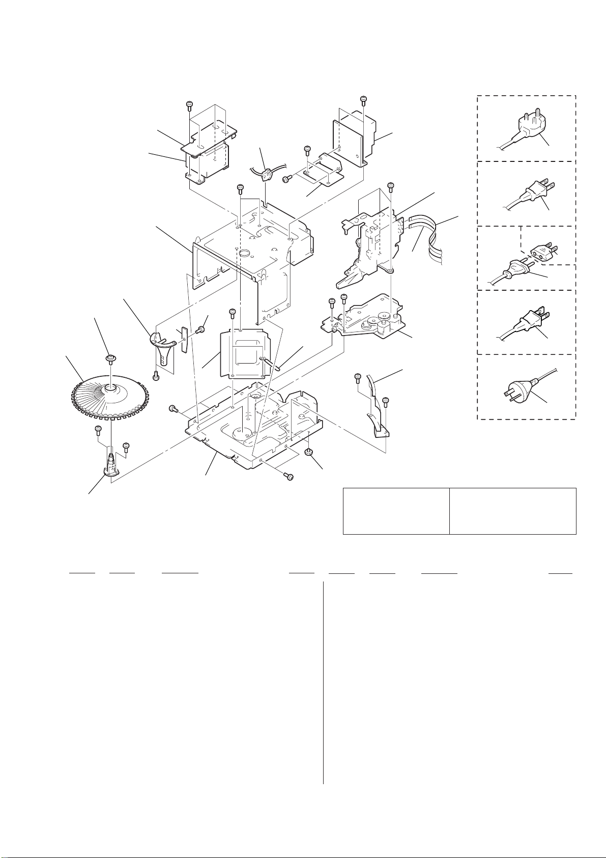
(3) CHASSIS SECTION
102
103
T109
104
107
not supplied
105
#1
#1
#2
not
supplied
106
#2
#3
108
#2
#4
109
not supplied
#6
#5
#1
#2
not supplied
#5
111
112
#1
not supplied
110
not supplied
UK
E
AEP, G,
SP
US, CND
AUS
114
114
SP
115
114
114
114
#3
#3
not supplied
#1
101
Ref. No. Part No. Description Remark
101 4-988-439-01 HOLDER, TABLE
102 4-988-434-11 TABLE (50)
103 4-957-577-31 SCREW PTP WH (2.6X8) (DIA. 10)
* 104 4-990-371-01 HOLDER (LED)
* 105 1-665-913-11 CD LED BOARD
106 4-951-620-01 SCREW (2.6X8), +BVTP
* 107 1-665-909-11 TRANS BOARD
* 108 3-703-244-00 BUSHING (2104), CORD (EXCEPT FR1: E)
108 3-703-571-11 BUSHING (S) (4516), CORD (FR1: E)
* 109 A-4398-376-A POWER AMP BOARD, COMPLETE (F50)
* 109 A-4398-382-A POWER AMP BOARD, COMPLETE (F100: US)
* 109 A-4398-403-A POWER AMP BOARD, COMPLETE
* 109 A-4398-416-A POWER AMP BOARD, COMPLETE
* 109 A-4398-748-A POWER AMP BOARD, COMPLETE (F100: CND)
(FR1: E, SP, AUS)
(FR1: AEP,UK,G)
113
The components identified by
mark ! or dotted line with
mark ! are critical for safety.
Replace only with part number
specified.
Ref. No. Part No. Description Remark
110 1-782-558-21 WIRE (FLAT TYPE) (16 CORE) (280mm)
110 1-782-560-21 WIRE (FLAT TYPE) (10 CORE) (F50)
111 1-782-559-21 WIRE (FLAT TYPE) (9 CORE)
* 112 4-990-370-01 COVER (CD)
113 4-965-822-01 FOOT
! 114 1-575-651-11 CORD, POWER (AEP, G, SP)
! 114 1-575-653-11 CORD, POWER (E)
! 114 1-690-608-11 CORD, POWER (AUS)
! 114 1-690-609-21 CORD, POWER (US, CND)
! 114 1-751-529-11 CORD, POWER (UK)
! 115 1-569-008-11 ADAPTOR, CONVERSION 2P (SP)
! T901 1-431-348-11 TRANSFORMER, POWER (F100: US)
! T901 1-431-349-11 TRANSFORMER, POWER (F100: CND)
! T901 1-431-350-11 TRANSFORMER, POWER (FR1: E, SP, AUS)
! T901 1-431-351-11 TRANSFORMER, POWER (FR1: AEP, UK, G)
Les composants identifiés par une
marque ! sont critiques pour la
sécurité.
Ne les remplacer que par une pièce
portant le neméro spécifié.
(F100/FR1)
! T901 1-431-352-11 TRANSFORMER, POWER (F50: US, CND)
– 97 –

(4) TAPE MECHANISM DECK SECTION-1
(TMC-220W2)
157
151
158
155
#7
159
#7
153
152
154
Ref. No. Part No. Description Remark
151 X-4946-663-1 HOLDER (L) ASSY, CASSETTE
152 X-4946-664-1 HOLDER (R) ASSY, CASSETTE
153 4-959-231-11 SPRING (L), TORSION
154 4-959-232-11 SPRING (R), TORSION
155 3-354-963-01 DAMPER
#7
156
Ref. No. Part No. Description Remark
* 156 4-980-439-01 FULCRUM, HOLDER
157 3-354-957-01 JOINT (LOCK LEVER)
* 158 3-354-953-01 LEVER (LOCK LEVER L)
* 159 3-354-954-01 LEVER (LOCK LEVER R)
155
not supplied
#3
157
– 98 –
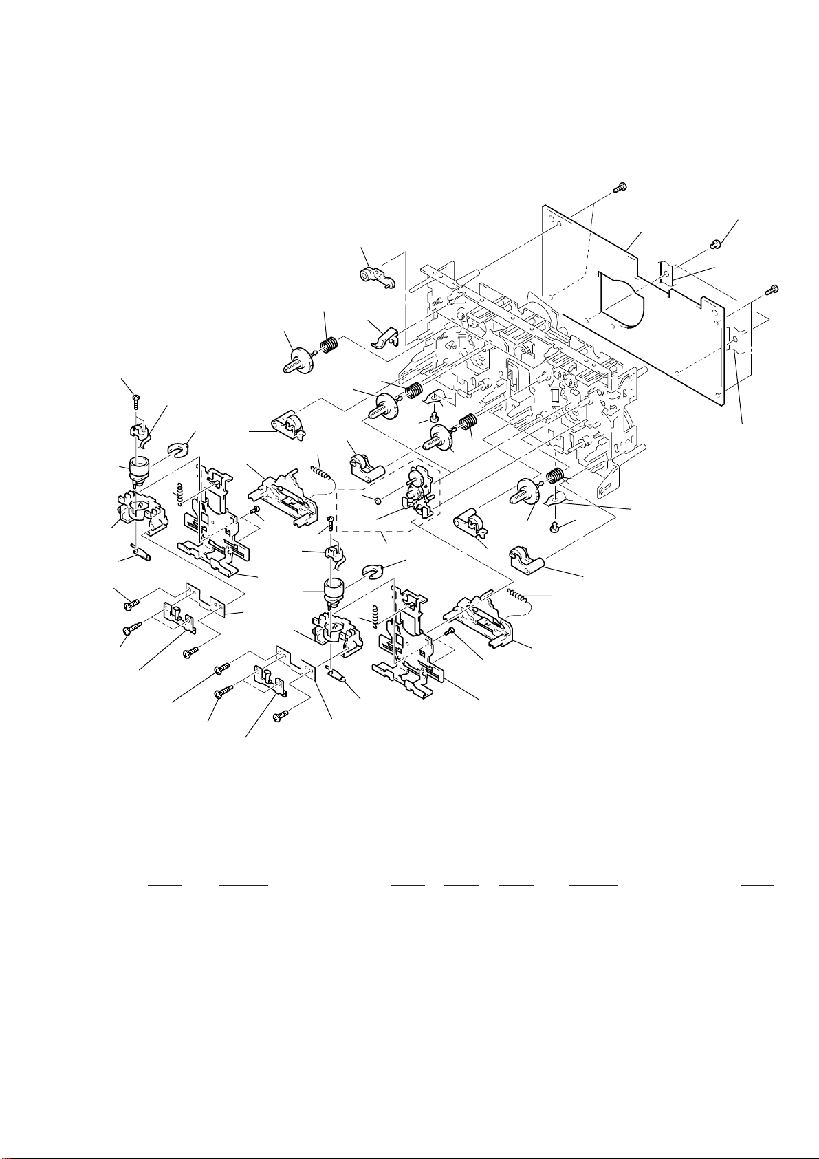
9
(5) TAPE MECHANISM DECK SECTION-2
(TCM-220WR2)
#9
not supplied
206
205
204
not supplied
202
201
HP101
(including
259
207
#8
•
A)
212
208
214
210
not supplied
HRPE101
(including
203
206
not supplied
205
211
•
215
B)
216
223
221
222
213
217
not supplied
209
218
219
207
•
214
A
215
212
210
216
208
211
222
219
213
220
(including
B
•
•
219
C)
A
•
•
#
B
not supplied
202
#8
not supplied
204
201
Ref. No. Part No. Description Remark
201 3-908-560-01 SPRING, AZIMUTH ADJUSTMENT
202 3-919-684-01 SCREW, AZIMUTH ADJUSTMENT
203 X-3373-113-1 SLIDER (HEAD) ASSY
204 3-908-556-01 SPRING, HEAD TOGGLE
205 3-908-558-02 FITTING BLOCK, HEAD
206 3-908-557-02 ROTARY BLOCK, HEAD
* 207 3-908-559-01 STOPPER, AZIMUTH
208 3-908-555-01 SLIDER (REV SLIDER)
209 3-917-143-11 SPRING, TENSION
210 3-388-848-01 SCREW (P2X6) (B TIGHT)
211 3-939-371-01 SPRING (1), TENSION
212 X-3369-909-1 PINCH LEVER (REV) ASSY
213 X-3369-908-1 PINCH LEVER (FWD) ASSY
203
Ref. No. Part No. Description Remark
214 3-908-613-01 GEAR (S), REEL
215 3-917-141-01 SPRING, COMPRESSION
216 X-3371-305-1 REEL (T) ASSY
217 3-669-465-01 WASHER (1.5), STOPPER
218 X-3370-173-1 TU ASSY
219 3-939-862-01 CLIP
* 220 A-2007-131-A AUDIO BOARD, COMPLETE
221 3-930-972-01 DETENT, HALF
222 3-917-142-01 SPRING, COMPRESSION
223 3-938-863-01 STOPPER
HP101 1-500-093-11 HEAD, MAGNETIC (PLAYBACK)
HRPE1011-500-094-11 HEAD, MAGNETIC (REC/PB/ERASE)
– 99 –

(6) TAPE MECHANISM DECK SECTION-3
(TCM-220WR2)
r C : MOTOR board (supplied with AUDIO board)
268
269
M2
r
C
263
252
272
259
267
266
264
#8
M1
265
257
263
270
#10
260
262
not supplied
261
#10
273
#11
260
258
255
254
253
257
256
252
#12
#13
271
#12
271
274
269
251
Ref. No. Part No. Description Remark
251 3-908-597-01 CAM (A)
252 3-908-608-11 SCREW, STEP
253 X-3372-930-1 ARM (A) ASSY, FR
254 X-3370-882-1 FLYWHEEL (AR) ASSY
255 3-928-047-01 PULLEY, TENSION
256 3-908-599-01 LEVER (REV-A)
257 3-908-601-01 SPRING (REV LEVER), TORSION
258 3-908-603-01 LEVER (TRIGGER A)
259 X-3367-593-1 FLYWHEEL (BF) ASSY
260 3-908-605-01 SPRING (TRIGGER), TORSION
261 3-908-609-01 GEAR, TRIGGER
262 3-913-845-11 BELT (A)
263 3-913-846-11 BELT (FR)
– 100 –
Ref. No. Part No. Description Remark
264 X-3370-171-1 FLYWHEEL (BR) ASSY
265 3-908-600-01 LEVER (REV-B)
* 266 1-650-669-11 LEAF SWITCH BOARD
267 3-908-598-01 CAM (B)
268 X-3372-931-1 ARM (B) ASSY, FR
269 3-914-111-01 SPRING (FR), TORSION
270 3-908-604-01 LEVER (TRIGGER B)
271 3-911-115-01 WASHER, STOPPER
272 3-917-176-11 BELT (B)
273 X-3370-172-1 FLYWHEEL (AF) ASSY
274 X-3371-441-1 CHASSIS ASSY, MECHANICAL
M1 X-3371-223-1 MOTOR ASSY, CAPSTAN
M2 A-2004-410-A MOTOR ASSY, DC (TRIGGER)

(7) MECHANISM DECK SECTION 1
321
327
324
326
326
324
325
316
318
317
not supplied
not supplied
A
215
314
320
312
311
310
313
309
308
304
303
301
302
305
306
307
328
319
323
322
A
#10
#10
#14
#10
#15
#10
#15
#16
not supplied
(CDM-46 B1: F100 / FR1)
(CDM-46 B2: F50)
Ref. No. Part No. Description Remark
* 301 1-663-975-11 SW BOARD
* 302 4-988-427-01 COVER, CAM
303 4-988-420-01 SLIDER (LOADING)
304 4-988-436-01 SPRING (LOADING), TORSION
305 4-988-418-01 HOLDER (A), DISC
* 306 4-988-417-01 SLIDER (CAM)
307 4-988-433-01 SLIDER (LOCK)
308 X-4948-020-1 LEVER (LOADING) ASSY
309 4-988-438-01 SPRING (LEVER), TENSION
310 4-988-437-01 SPRING (HOLDER), TORSION
Ref. No. Part No. Description Remark
* 315 4-988-421-01 HOLDER (MAGNET)
316 A-4672-385-A MAGNET ASSY
317 4-960-633-01 YOKE (MAGNET)
318 4-960-632-11 PULLEY (B)
* 319 4-976-473-01 HOLDER (LED-S)
320 4-988-431-01 ROLLER (DISC)
321 X-4948-019-1 HOLDER ASSY, BU
322 1-777-874-11 WIRE (FLAT TYPE) (16 CORE) (75mm)
* 323 1-663-973-11 DISC SENSOR (S) BOARD
324 4-988-440-01 SPRING (F-1), TENSION
* 311 4-988-416-01 BASE, LOADING
312 4-988-419-01 HOLDER (B), DISC
313 4-992-069-01 SCREW (+PTPWH) (M2) (DIA. 7)
* 314 4-988-454-01 COVER (LEVER)
325 4-988-441-01 SPRING (F-2), TENSION
326 4-957-577-21 SCREW PTP WH (2.6X8) (DIA. 10)
327 4-992-413-02 STOPPER
328 3-910-095-11 RUBBER, VIBRATION PROOF
– 101 –

(8) MECHANISM DECK SECTION 2
(CDM-46 B1: F100 / FR1)
(CDM-46 B2: F50)
351
#17
355
354
352
354
353
356
#17
#14
358
#20
360
M602
359
Ref. No. Part No. Description Remark
* 351 1-663-971-11 TABLE SENSOR BOARD
352 4-988-414-01 BELT
353 4-988-423-01 GEAR (A) (LOADING)
354 4-988-425-01 PULLEY
355 4-988-424-01 GEAR (TABLE)
357
M601
#1
Ref. No. Part No. Description Remark
* 357 4-988-426-01 BASE (CDM)
* 358 1-663-972-11 DISC SENSOR (R) BOARD
* 359 1-663-974-11 CD MOTOR BOARD
* 360 4-990-669-01 HOLDER (SENSOR)
M61 X-4948-434-1 MOTOR ASSY (LOADING)
356 4-988-432-01 GEAR (B) (LOADING)
M62 X-4948-434-1 MOTOR ASSY (TABLE)
– 102 –

(9) OPTICAL PICK UP SECTION
(KSM-213 BFN/M-NP)
not supplied
403
#19
406
M102
406
M101
406
404
401
402
406
405
Ref. No. Part No. Description Remark
! 401 8-848-379-31 OPTICAL PICK-UP KSS-213B/S-N
402 2-626-907-01 GEAR (A) (S)
403 2-627-003-02 GEAR (B) (RP)
404 2-626-908-01 SHAFT, SLED
* 405 A-4699-536-A BD BOARD, COMPLETE (F50)
– 103 –
#18
The components identified by
mark ! or dotted line with
mark ! are critical for safety.
Replace only with part number
specified.
Ref. No. Part No. Description Remark
* 405 A-4699-675-A BD BOARD, COMPLETE (F100/FR1)
* 406 4-992-054-01 RUBBER, VIBRATION PROOF
M101 X-2646-110-1 T, T CHASSIS ASSY (MG) (F) (SPINDLE)
M102 X-2625-769-1 MOTOR GEAR ASSY (MB) (RP) (SLED)
Les composants identifiés par une
marque ! sont critiques pour la
sécurité.
Ne les remplacer que par une pièce
portant le neméro spécifié.

AUDIO
SECTION 8
ELECTRICAL PARTS LIST
NOTE:
• Due to standardization, replacements in the
parts list may be different from the parts specified in the diagrams or the components used on
the set.
• -XX and -X mean standardized parts, so they
may have some difference from the original one.
• RESISTORS
All resistors are in ohms.
METAL: Metal-film resistor.
METAL OXIDE: Metal oxide-film resistor.
F: nonflammable
• Items marked “*” are not stocked since they
are seldom required for routine service.
Some delay should be anticipated when ordering these items.
Ref. No. Part No. Description Remark
A-2007-131-A AUDIO BOARD, COMPLETE
**********************
< CAPACITOR >
C301 1-162-289-31 CERAMIC 390PF 10% 50V
C302 1-126-968-11 ELECT 100uF 20% 6.3V
C303 1-162-282-31 CERAMIC 100PF 10% 50V
C304 1-130-483-00 MYLAR 0.01uF 5% 50V
C305 1-107-715-11 ELECT 22uF 20% 16V
• SEMICONDUCTORS
In each case, u: µ, for example:
uA. . : µA. . uPA. . : µPA. .
uPB. . : µPB. . uPC. . : µPC. .
uPD. . : µPD. .
• CAPACITORS
uF: µF
• COILS
uH: µH
• Abbreviation
CND : Canadian
G : German
SP : Singapore
The components identified by mark
! or dotted line with mark ! are
critical for safety.
Replace only with part number
specified.
Les composants identifiés par une
marque ! sont critiquens pour la
sécurité.
Ne les remplacer que par une pièce
portant le neméro spécifié.
When indicating parts by reference
number, please include the board.
Ref. No. Part No. Description Remark
CN602 1-564-718-11 PIN, CONNECTOR (SMALL TYPE) 2P
* CN651 1-564-521-11 PLUG, CONNECTOR 6P
< IC >
IC601 8-759-111-44 IC uPC4570C-1
IC602 8-759-143-54 IC uPC1330HA
IC611 8-759-111-44 IC uPC4570C-1
< COIL >
C311 1-162-289-31 CERAMIC 390PF 10% 50V
C313 1-162-282-31 CERAMIC 100PF 10% 50V
C314 1-130-487-00 MYLAR 0.022uF 5% 50V
C315 1-126-233-11 ELECT 22uF 20% 50V
C331 1-137-427-11 FILM 120PF 5% 50V
C332 1-162-288-31 CERAMIC 330PF 10% 50V
C333 1-162-209-31 CERAMIC 27PF 5% 50V
C401 1-162-289-31 CERAMIC 390PF 10% 50V
C402 1-126-968-11 ELECT 100uF 20% 6.3V
C403 1-162-282-31 CERAMIC 100PF 10% 50V
C404 1-130-483-00 MYLAR 0.01uF 5% 50V
C405 1-107-715-11 ELECT 22uF 20% 16V
C411 1-162-289-31 CERAMIC 390PF 10% 50V
C413 1-162-282-31 CERAMIC 100PF 10% 50V
C414 1-130-487-00 MYLAR 0.022uF 5% 50V
C415 1-126-233-11 ELECT 22uF 20% 50V
C431 1-137-427-11 FILM 120PF 5% 50V
C432 1-162-288-31 CERAMIC 330PF 10% 50V
C433 1-162-209-31 CERAMIC 27PF 5% 50V
C601 1-104-396-11 ELECT 10uF 20% 16V
C602 1-104-396-11 ELECT 10uF 20% 16V
C611 1-124-907-11 ELECT 10uF 20% 50V
C612 1-124-907-11 ELECT 10uF 20% 50V
C621 1-137-150-11 FILM 0.01uF 5% 100V
C622 1-126-961-11 ELECT 2.2uF 20% 50V
L331 1-410-780-11 INDUCTOR 27mH
L431 1-410-780-11 INDUCTOR 27mH
< TRANSISTOR >
Q621 8-729-142-46 TRANSISTOR 2SC2001-LK
Q622 8-729-142-46 TRANSISTOR 2SC2001-LK
Q623 8-729-801-93 TRANSISTOR 2SD1387
Q651 8-729-900-65 TRANSISTOR DTA144ES
< RESISTOR >
R301 1-247-881-00 CARBON 120K 5% 1/4W
R302 1-249-409-11 CARBON 220 5% 1/4W
R303 1-249-433-11 CARBON 22K 5% 1/4W
R304 1-247-889-00 CARBON 270K 5% 1/4W
R305 1-247-858-11 CARBON 13K 5% 1/4W
R311 1-247-881-00 CARBON 120K 5% 1/4W
R312 1-247-807-31 CARBON 100 5% 1/4W
R314 1-247-882-11 CARBON 130K 5% 1/4W
R315 1-247-850-11 CARBON 6.2K 5% 1/4W
R331 1-249-430-11 CARBON 12K 5% 1/4W
R401 1-247-881-00 CARBON 120K 5% 1/4W
R402 1-249-409-11 CARBON 220 5% 1/4W
R403 1-249-433-11 CARBON 22K 5% 1/4W
R404 1-247-889-00 CARBON 270K 5% 1/4W
R405 1-247-858-11 CARBON 13K 5% 1/4W
C623 1-136-155-00 FILM 0.015uF 5% 50V
C624 1-130-481-00 MYLAR 0.0068uF 5% 50V
C625 1-130-481-00 MYLAR 0.0068uF 5% 50V
C627 1-124-903-11 ELECT 1uF 20% 50V
C628 1-136-153-00 FILM 0.01uF 5% 50V
C642 1-104-664-11 ELECT 47uF 20% 16V
< CONNECTOR >
CN601 1-695-382-31 PIN, CONNECTOR (PC BOARD) 21P
R411 1-247-881-00 CARBON 120K 5% 1/4W
R412 1-247-807-31 CARBON 100 5% 1/4W
R414 1-247-882-11 CARBON 130K 5% 1/4W
R415 1-247-850-11 CARBON 6.2K 5% 1/4W
R431 1-249-430-11 CARBON 12K 5% 1/4W
R601 1-249-409-11 CARBON 220 5% 1/4W
R602 1-249-409-11 CARBON 220 5% 1/4W
R608 1-249-409-11 CARBON 220 5% 1/4W
R609 1-249-433-11 CARBON 22K 5% 1/4W
R611 1-249-409-11 CARBON 220 5% 1/4W
– 104 –

AUDIO BD
Ref. No. Part No. Description Remark
R612 1-249-409-11 CARBON 220 5% 1/4W
! R621 1-212-851-00 FUSIBLE 5.6 5% 1/4W F
! R622 1-212-851-00 FUSIBLE 5.6 5% 1/4W F
R623 1-249-432-11 CARBON 18K 5% 1/4W
R624 1-249-432-11 CARBON 18K 5% 1/4W
R625 1-249-429-11 CARBON 10K 5% 1/4W
R651 1-247-856-00 CARBON 11K 5% 1/4W
R652 1-247-856-00 CARBON 11K 5% 1/4W
R653 1-249-441-11 CARBON 100K 5% 1/4W
< VARIABLE RESISTOR >
RV301 1-238-598-11 RES, ADJ, CARBON 2.2K
RV311 1-238-598-11 RES, ADJ, CARBON 2.2K
RV341 1-238-551-11 RES, ADJ, CARBON 220K
RV401 1-238-598-11 RES, ADJ, CARBON 2.2K
RV411 1-238-598-11 RES, ADJ, CARBON 2.2K
RV441 1-238-551-11 RES, ADJ, CARBON 220K
RV651 1-238-599-11 RES, ADJ, CARBON 4.7K
RV652 1-238-599-11 RES, ADJ, CARBON 4.7K
< TRANSFORMER >
T621 1-423-980-11 TRANSFORMER, BIAS OSCILLATION
************************************************************
Ref. No. Part No. Description Remark
C128 1-163-809-11 CERAMIC CHIP 0.047uF 10% 25V
C129 1-110-501-11 CERAMIC CHIP 0.33uF 10% 16V
C130 1-124-443-00 ELECT 100uF 20% 10V
C131 1-163-009-11 CERAMIC CHIP 0.001uF 10% 50V
C132 1-163-038-00 CERAMIC CHIP 0.1uF 25V
C133 1-163-038-00 CERAMIC CHIP 0.1uF 25V
C141 1-163-038-00 CERAMIC CHIP 0.1uF 25V
C142 1-164-505-11 CERAMIC CHIP 2.2uF 16V
C151 1-107-725-11 CERAMIC CHIP 0.1uF 10% 16V
C152 1-107-725-11 CERAMIC CHIP 0.1uF 10% 16V
C153 1-107-725-11 CERAMIC CHIP 0.1uF 10% 16V
C154 1-163-009-11 CERAMIC CHIP 0.001uF 10% 50V
C155 1-163-093-00 CERAMIC CHIP 10PF 5% 50V
C156 1-163-085-00 CERAMIC CHIP 2PF 50V
C157 1-164-232-11 CERAMIC CHIP 0.01uF 50V
C158 1-163-038-00 CERAMIC CHIP 0.1uF 25V
C159 1-163-101-00 CERAMIC CHIP 22PF 5% 50V
C160 1-163-117-00 CERAMIC CHIP 100PF 5% 50V
C161 1-163-038-00 CERAMIC CHIP 0.1uF 25V
C162 1-163-038-00 CERAMIC CHIP 0.1uF 25V
C163 1-163-038-00 CERAMIC CHIP 0.1uF 25V
C164 1-163-227-11 CERAMIC CHIP 10PF 0.5PF 50V
C165 1-163-227-11 CERAMIC CHIP 10PF 0.5PF 50V
* A-4699-536-A BD BOARD, COMPLETE (F50)
* A-4699-675-A BD BOARD, COMPLETE (F100/FR1)
********************
< CAPACITOR >
C101 1-163-038-00 CERAMIC CHIP 0.1uF 25V
C102 1-163-038-00 CERAMIC CHIP 0.1uF 25V
C103 1-164-489-11 CERAMIC CHIP 0.22uF 10% 16V
C104 1-163-003-11 CERAMIC CHIP 330PF 10% 50V
C105 1-163-023-00 CERAMIC CHIP 0.015uF 5% 50V
C106 1-110-501-11 CERAMIC CHIP 0.33uF 10% 16V
C107 1-163-989-11 CERAMIC CHIP 0.033uF 10% 25V
C108 1-164-492-11 CERAMIC CHIP 0.15uF 10% 16V
C109 1-163-013-11 CERAMIC CHIP 0.0022uF 10% 50V
C110 1-163-037-11 CERAMIC CHIP 0.022uF 10% 50V
C111 1-163-989-11 CERAMIC CHIP 0.033uF 10% 25V
C112 1-163-009-11 CERAMIC CHIP 0.001uF 10% 50V
C113 1-164-492-11 CERAMIC CHIP 0.15uF 10% 16V
C114 1-164-492-11 CERAMIC CHIP 0.15uF 10% 16V
C115 1-164-232-11 CERAMIC CHIP 0.01uF 50V
C116 1-164-232-11 CERAMIC CHIP 0.01uF 50V
C117 1-163-001-11 CERAMIC CHIP 220PF 10% 50V
C118 1-107-823-11 CERAMIC CHIP 0.47uF 10% 16V
C119 1-164-489-11 CERAMIC CHIP 0.22uF 10% 16V
C120 1-124-234-00 ELECT 22uF 20% 16V
C121 1-164-182-11 CERAMIC CHIP 0.0033uF 10% 50V
C122 1-126-963-11 ELECT 4.7uF 20% 50V
C123 1-163-038-00 CERAMIC CHIP 0.1uF 25V
C124 1-104-396-11 ELECT 10uF 20% 16V
C125 1-123-661-11 ELECT 100uF 20% 6.3V
C126 1-123-661-11 ELECT 100uF 20% 6.3V
C127 1-163-989-11 CERAMIC CHIP 0.033uF 10% 25V
C166 1-124-443-00 ELECT 100uF 20% 10V
C167 1-163-038-00 CERAMIC CHIP 0.1uF 25V
C171 1-163-038-00 CERAMIC CHIP 0.1uF 25V
C172 1-123-661-11 ELECT 100uF 20% 6.3V
C173 1-124-589-11 ELECT 47uF 20% 16V
C174 1-163-038-00 CERAMIC CHIP 0.1uF 25V
(F100/FR1)
C175 1-163-038-00 CERAMIC CHIP 0.1uF 25V
C181 1-104-664-11 ELECT 47uF 20% 16V
C182 1-104-664-11 ELECT 47uF 20% 16V
C183 1-163-003-11 CERAMIC CHIP 330PF 10% 50V
C184 1-163-003-11 CERAMIC CHIP 330PF 10% 50V
< CONNECTOR >
CN101 1-770-173-11 CONNECTOR, FFC/FPC 16P
CN102 1-568-853-11 SOCKET, CONNECTOR 10P (F50)
CN102 1-691-894-21 SOCKET, CONNECTOR 16P (F100/FR1)
* CN103 1-568-852-11 SOCKET, CONNECTOR 9P
< DIODE >
D151 8-719-987-63 DIODE 1N4148M (F100/FR1)
< IC >
IC101 8-759-449-64 IC LA9240M
IC102 8-759-449-65 IC LC78622E
IC103 8-759-449-66 IC LA6541
IC104 8-759-428-57 IC LC89170M (F100/FR1)
< JUMPER RESISTOR >
JW1 1-216-295-00 CONDUCTOR, CHIP (2012)
JW2 1-216-295-00 CONDUCTOR, CHIP (2012)
JW3 1-216-295-00 CONDUCTOR, CHIP (2012) (F50)
– 105 –
The components identified by
mark ! or dotted line with
mark ! are critical for safety.
Replace only with part number
specified.
Les composants identifiés par une
marque ! sont critiques pour la
sécurité.
Ne les remplacer que par une pièce
portant le neméro spécifié.

BD CD DOOR CD LED
Ref. No. Part No. Description Remark
JW4 1-216-295-00 CONDUCTOR, CHIP (2012) (F100/FR1)
JW5 1-216-295-00 CONDUCTOR, CHIP (2012) (F100/FR1)
JW6 1-216-295-00 CONDUCTOR, CHIP (2012)
JW7 1-216-295-00 CONDUCTOR, CHIP (2012)
JW8 1-216-295-00 CONDUCTOR, CHIP (2012)
JW9 1-216-295-00 CONDUCTOR, CHIP (2012)
JW10 1-216-295-00 CONDUCTOR, CHIP (2012)
< TRANSISTOR >
Q101 8-729-119-78 TRANSISTOR 2SC403SP-51
Q102 8-729-119-78 TRANSISTOR 2SC403SP-51
Q103 8-729-119-76 TRANSISTOR 2SA1175-HFE
< RESISTOR >
R101 1-216-097-00 METAL GLAZE 100K 5% 1/10W
R102 1-216-093-00 METAL CHIP 68K 5% 1/10W
R103 1-216-093-00 METAL CHIP 68K 5% 1/10W
R104 1-216-093-00 METAL CHIP 68K 5% 1/10W
R105 1-216-093-00 METAL CHIP 68K 5% 1/10W
R106 1-216-097-00 METAL GLAZE 100K 5% 1/10W
R107 1-216-097-00 METAL GLAZE 100K 5% 1/10W
R108 1-216-068-00 METAL CHIP 6.2K 5% 1/10W
R109 1-216-076-00 METAL CHIP 13K 5% 1/10W
R110 1-216-093-00 METAL CHIP 68K 5% 1/10W
R111 1-216-057-00 METAL CHIP 2.2K 5% 1/10W
R112 1-216-109-00 METAL CHIP 330K 5% 1/10W
R113 1-216-099-00 METAL CHIP 120K 5% 1/10W
R114 1-216-055-00 METAL CHIP 1.8K 5% 1/10W
R115 1-216-087-11 METAL CHIP 39K 5% 1/10W
Ref. No. Part No. Description Remark
R158 1-216-049-11 METAL GLAZE 1K 5% 1/10W
R159 1-216-083-00 METAL CHIP 27K 5% 1/10W
R160 1-216-037-00 METAL CHIP 330 5% 1/10W
R161 1-216-073-00 METAL CHIP 10K 5% 1/10W
R162 1-216-037-00 METAL CHIP 330 5% 1/10W
(F100/FR1)
R163 1-216-049-11 METAL GLAZE 1K 5% 1/10W
R164 1-216-065-00 METAL CHIP 4.7K 5% 1/10W
R165 1-216-025-00 METAL GLAZE 100 5% 1/10W
R166 1-216-025-00 METAL GLAZE 100 5% 1/10W
R171 1-216-025-00 METAL GLAZE 100 5% 1/10W
(F100/FR1)
R172 1-216-025-00 METAL GLAZE 100 5% 1/10W
(F100/FR1)
R173 1-216-025-00 METAL GLAZE 100 5% 1/10W
(F100/FR1)
R174 1-216-025-00 METAL GLAZE 100 5% 1/10W
(F100/FR1)
R181 1-216-057-00 METAL CHIP 2.2K 5% 1/10W
R182 1-216-057-00 METAL CHIP 2.2K 5% 1/10W
R183 1-216-073-00 METAL CHIP 10K 5% 1/10W
R184 1-216-073-00 METAL CHIP 10K 5% 1/10W
R191 1-216-025-00 METAL GLAZE 100 5% 1/10W
R192 1-216-041-00 METAL CHIP 470 5% 1/10W
R193 1-216-041-00 METAL CHIP 470 5% 1/10W
R194 1-216-025-00 METAL GLAZE 100 5% 1/10W
R195 1-216-041-00 METAL CHIP 470 5% 1/10W
R196 1-216-025-00 METAL GLAZE 100 5% 1/10W
R197 1-216-025-00 METAL GLAZE 100 5% 1/10W
R116 1-216-057-00 METAL CHIP 2.2K 5% 1/10W
R117 1-216-085-00 METAL CHIP 33K 5% 1/10W
R118 1-216-081-00 METAL CHIP 22K 5% 1/10W
R119 1-216-069-00 METAL CHIP 6.8K 5% 1/10W
R120 1-216-085-00 METAL CHIP 33K 5% 1/10W
R121 1-216-059-00 METAL CHIP 2.7K 5% 1/10W
R122 1-216-083-00 METAL CHIP 27K 5% 1/10W
R123 1-216-099-00 METAL CHIP 120K 5% 1/10W
R124 1-216-093-00 METAL CHIP 68K 5% 1/10W
R125 1-216-089-00 METAL GLAZE 47K 5% 1/10W
R126 1-216-037-00 METAL CHIP 330 5% 1/10W
R127 1-216-089-00 METAL GLAZE 47K 5% 1/10W
R128 1-216-077-00 METAL CHIP 15K 5% 1/10W
R129 1-216-069-00 METAL CHIP 6.8K 5% 1/10W
R130 1-216-113-00 METAL CHIP 470K 5% 1/10W
R131 1-216-113-00 METAL CHIP 470K 5% 1/10W
R132 1-216-065-00 METAL CHIP 4.7K 5% 1/10W
R133 1-216-113-00 METAL CHIP 470K 5% 1/10W
R134 1-216-113-00 METAL CHIP 470K 5% 1/10W
R135 1-216-065-00 METAL CHIP 4.7K 5% 1/10W
R136 1-216-073-00 METAL CHIP 10K 5% 1/10W
R137 1-216-009-00 METAL CHIP 22 5% 1/10W
R138 1-216-089-00 METAL GLAZE 47K 5% 1/10W
R151 1-216-045-00 METAL CHIP 680 5% 1/10W
R152 1-216-093-00 METAL CHIP 68K 5% 1/10W
R153 1-216-051-00 METAL CHIP 1.2K 5% 1/10W
R154 1-216-085-00 METAL CHIP 33K 5% 1/10W
R155 1-216-089-00 METAL GLAZE 47K 5% 1/10W
R156 1-216-081-00 METAL CHIP 22K 5% 1/10W
R157 1-216-077-00 METAL CHIP 15K 5% 1/10W
< SWITCH >
S101 1-572-085-11 SWITCH, LEAF (LIMIT)
< VIBRATOR >
X101 1-577-576-21 VIBRATOR, CRYSTAL (16.9344MHz)
************************************************************
* 1-665-910-11 CD DOOR BOARD
**************
< SWITCH >
S413 1-762-936-11 SWITCH, LEVER (DOOR DET)
************************************************************
* 1-665-913-11 CD LED BOARD
*************
< CONNECTOR >
CN904 1-506-481-11 PIN, CONNECTOR 2P
< LED >
D391 8-719-058-64 LED SEL5823A-TP15
D392 8-719-058-64 LED SEL5823A-TP15
D393 8-719-058-04 LED SEL5223S-TP15
D394 8-719-058-03 LED SEL5423E-TP15
< RESISTOR >
R395 1-249-412-11 CARBON 390 5% 1/4W
************************************************************
– 106 –

DISC SENSOR (R)CD MOTOR
DISC SENSOR (S)
Ref. No. Part No. Description Remark Ref. No. Part No. Description Remark
* 1-663-974-11 CD MOTOR BOARD
CN61 1-506-469-11 PIN, CONNECTOR 4P
************************************************************
* 1-663-972-11 DISC SENSOR (R) BOARD
* 4-990-669-01 HOLDER (SENSOR)
7-685-132-19 SCREW +BTP 2.6X5 TYPE2 N-S
Q51 8-729-926-31 PHOTO TRANSISTOR PT483F1S
************************************************************
* 1-663-973-11 DISC SENSOR (S) BOARD
* 4-976-473-01 HOLDER (LED-S)
* CN53 1-568-951-11 PIN, CONNECTOR 2P
D51 8-719-055-84 DIODE GL-528VS1
****************
< CONNECTOR >
*********************
< TRANSISTOR >
*********************
< CONNECTOR >
< DIODE >
IC751 8-759-634-50 IC M5218AL (FR1: SP)
J751 1-573-151-11 JACK, LARGE TYPE (MIC) (FR1: SP)
J771 1-573-151-11 JACK, LARGE TYPE (PHONES)
R751 1-249-429-11 CARBON 10K 5% 1/4W
R752 1-249-417-11 CARBON 1K 5% 1/4W
R753 1-249-441-11 CARBON 100K 5% 1/4W
R754 1-249-417-11 CARBON 1K 5% 1/4W
R755 1-249-433-11 CARBON 22K 5% 1/4W
R761 1-249-429-11 CARBON 10K 5% 1/4W
R762 1-247-885-00 CARBON 180K 5% 1/4W
R763 1-249-409-11 CARBON 220 5% 1/4W
R764 1-247-903-00 CARBON 1M 5% 1/4W
HP/MIC
< IC >
< JACK >
< RESISTOR >
LEAF SWITCH
(FR1: SP)
(FR1: SP)
(FR1: SP)
(FR1: SP)
(FR1: SP)
(FR1: SP)
(FR1: SP)
(FR1: SP)
(FR1: SP)
< RESISTOR >
R54 1-249-409-11 CARBON 220 5% 1/4W
************************************************************
* 1-665-908-11 HP/MIC BOARD
*************
< CAPACITOR >
C751 1-126-961-11 ELECT 2.2uF 20% 50V
(FR1: SP)
C752 1-162-294-31 CERAMIC 0.001uF 10% 50V
(FR1: SP)
C754 1-162-215-31 CERAMIC 47PF 5% 50V
(FR1: SP)
C755 1-162-293-31 CERAMIC 820PF 10% 50V
(FR1: SP)
C756 1-126-959-11 ELECT 0.47uF 20% 50V
(FR1: SP)
C761 1-162-215-31 CERAMIC 47PF 5% 50V
(FR1: SP)
C763 1-126-964-11 ELECT 10uF 20% 50V
(FR1: SP)
C765 1-164-159-11 CERAMIC 0.1uF 50V
(FR1: SP)
C766 1-164-159-11 CERAMIC 0.1uF 50V
(FR1: SP)
C776 1-164-159-11 CERAMIC 0.1uF 50V
< VARIABLE RESISTOR >
RV751 1-225-458-11 RES, VAR, CARBON 50K (FR1: SP) (MIC-VOL)
************************************************************
* 1-650-669-11 LEAF SWITCH BOARD
******************
< CONNECTOR >
* CN1001 1-568-854-11 SOCKET, CONNECTOR 11P
< TRANSISTOR >
Q1001 8-749-010-90 TRANSISTOR PHOTO REFLECTOR NJL5165KA-H
Q1002 8-749-010-90 TRANSISTOR PHOTO REFLECTOR NJL5165KA-H
< RESISTOR >
R1001 1-247-818-11 CARBON 300 5% 1/4W
R1002 1-247-820-11 CARBON 360 5% 1/4W
R1003 1-249-414-11 CARBON 560 5% 1/4W
R1004 1-247-834-11 CARBON 1.3K 5% 1/4W
R1005 1-247-818-11 CARBON 300 5% 1/4W
< SWITCH >
S1001 1-692-832-11 SWITCH, PUSH (1 KEY) (A PLAY)
S1002 1-692-832-11 SWITCH, PUSH (1 KEY) (B PLAY)
S1003 1-572-248-11 SWITCH, LEAF (A HALF)
S1004 1-571-281-21 SWITCH, LEAF (A CrO2)
S1005 1-571-281-21 SWITCH, LEAF (REC A)
< CONNECTOR >
* CN751 1-568-453-11 PIN, CONNECTOR (PC BOARD) 4P
(EXCEPT FR1: SP)
* CN751 1-566-973-11 PIN, CONNECTOR (PC BOARD) 8P (FR1: SP)
S1006 1-572-248-11 SWITCH, LEAF (B HALF)
S1008 1-571-281-21 SWITCH, LEAF (B CrO2)
S1009 1-571-281-21 SWITCH, LEAF (REC B)
************************************************************
– 107 –

MAIN
Ref. No. Part No. Description Remark
* A-4398-366-A MAIN BOARD, COMPLETE (F50)
* A-4398-368-A MAIN BOARD, COMPLETE (F100)
* A-4398-394-A MAIN BOARD, COMPLETE (FR1: SP)
* A-4398-400-A MAIN BOARD, COMPLETE (FR1: E)
* A-4398-408-A MAIN BOARD, COMPLETE (FR1: AUS)
* A-4398-413-A MAIN BOARD, COMPLETE (FR1: AEP, UK, G)
**********************
7-685-646-79 SCREW +BVTP 3X8 TYPE2 N-S
< CAPACITOR >
C121 1-162-286-31 CERAMIC 220PF 10% 50V
(FR1: AEP, UK, G)
C122 1-162-286-31 CERAMIC 220PF 10% 50V
(FR1: AEP, UK, G)
C123 1-162-306-11 CERAMIC 0.01uF 20% 16V
C131 1-130-493-00 MYLAR 0.068uF 5% 50V
(FR1: AEP, UK, G)
C132 1-130-493-00 MYLAR 0.068uF 5% 50V
(FR1: AEP, UK, G)
C140 1-126-960-11 ELECT 1uF 20% 50V
(F100/FR1)
C171 1-162-286-31 CERAMIC 220PF 10% 50V
(FR1: AEP, UK, G)
C172 1-162-286-31 CERAMIC 220PF 10% 50V
(FR1: AEP, UK, G)
C173 1-162-306-11 CERAMIC 0.01uF 20% 16V
C181 1-130-493-00 MYLAR 0.068uF 5% 50V
(FR1: AEP, UK, G)
C182 1-130-493-00 MYLAR 0.068uF 5% 50V
(FR1: AEP, UK, G)
C191 1-126-963-11 ELECT 4.7uF 20% 50V
(F100/FR1)
C192 1-164-159-11 CERAMIC 0.1uF 50V
(F100/FR1)
C201 1-136-169-00 FILM 0.22uF 5% 50V
C202 1-136-169-00 FILM 0.22uF 5% 50V
C203 1-130-493-00 MYLAR 0.068uF 5% 50V
C204 1-130-493-00 MYLAR 0.068uF 5% 50V
C205 1-130-486-00 MYLAR 0.018uF 10% 50V
C206 1-130-486-00 MYLAR 0.018uF 10% 50V
C207 1-130-480-00 MYLAR 0.0056uF 5% 50V
C208 1-130-479-00 MYLAR 0.0047uF 5% 50V
C209 1-130-474-00 MYLAR 0.0018uF 5% 50V
C210 1-126-964-11 ELECT 10uF 20% 50V
C211 1-126-964-11 ELECT 10uF 20% 50V
C212 1-130-481-00 MYLAR 0.0068uF 5% 50V
C213 1-136-165-00 FILM 0.1uF 5% 50V
C214 1-136-165-00 FILM 0.1uF 5% 50V
C215 1-130-471-00 MYLAR 0.001uF 5% 50V
(FR1: SP)
C216 1-136-167-00 FILM 0.15uF 5% 50V
(FR1: SP)
C217 1-126-964-11 ELECT 10uF 20% 50V
(F100/FR1)
C221 1-126-933-11 ELECT 100uF 20% 10V
C222 1-126-933-11 ELECT 100uF 20% 10V
C223 1-126-964-11 ELECT 10uF 20% 50V
C224 1-162-290-31 CERAMIC 470PF 10% 50V
C226 1-126-964-11 ELECT 10uF 20% 50V
C231 1-126-960-11 ELECT 1uF 20% 50V
Ref. No. Part No. Description Remark
C242 1-162-292-31 CERAMIC 680PF 10% 50V
(F100/FR1)
C243 1-126-964-11 ELECT 10uF 20% 50V
(F100/FR1)
C244 1-162-286-31 CERAMIC 220PF 10% 50V
(FR1: AEP, UK, G)
C245 1-162-306-11 CERAMIC 0.01uF 20% 16V
(F100/FR1)
C246 1-162-306-11 CERAMIC 0.01uF 20% 16V
(F100/FR1)
C247 1-164-159-11 CERAMIC 0.1uF 50V
(F50/F100/FR1: AEP, UK, G)
C251 1-136-169-00 FILM 0.22uF 5% 50V
C252 1-136-169-00 FILM 0.22uF 5% 50V
C253 1-130-493-00 MYLAR 0.068uF 5% 50V
C254 1-130-493-00 MYLAR 0.068uF 5% 50V
C255 1-130-486-00 MYLAR 0.018uF 10% 50V
C256 1-130-486-00 MYLAR 0.018uF 10% 50V
C257 1-130-480-00 MYLAR 0.0056uF 5% 50V
C258 1-130-479-00 MYLAR 0.0047uF 5% 50V
C259 1-130-474-00 MYLAR 0.0018uF 5% 50V
C260 1-126-964-11 ELECT 10uF 20% 50V
C261 1-126-964-11 ELECT 10uF 20% 50V
C262 1-130-481-00 MYLAR 0.0068uF 5% 50V
C263 1-136-165-00 FILM 0.1uF 5% 50V
C264 1-136-165-00 FILM 0.1uF 5% 50V
C267 1-126-964-11 ELECT 10uF 20% 50V
(F100/FR1)
C276 1-126-964-11 ELECT 10uF 20% 50V
C278 1-126-965-11 ELECT 22uF 20% 50V
C279 1-126-965-11 ELECT 22uF 20% 50V
C281 1-126-933-11 ELECT 100uF 20% 10V
C282 1-126-961-11 ELECT 2.2uF 20% 50V
C283 1-126-933-11 ELECT 100uF 20% 10V
(F100)
C283 1-126-923-11 ELECT 220uF 20% 10V
(F50/FR1)
C284 1-126-923-11 ELECT 220uF 20% 10V
C291 1-126-959-11 ELECT 0.47uF 20% 50V
C295 1-162-306-11 CERAMIC 0.01uF 20% 16V
(F100/FR1)
C296 1-126-933-11 ELECT 100uF 20% 10V
(F100/FR1)
C301 1-126-967-11 ELECT 47uF 20% 16V
C302 1-164-159-11 CERAMIC 0.1uF 50V
C303 1-136-173-00 FILM 0.47uF 5% 50V
C304 1-126-916-11 ELECT 1000uF 20% 6.3V
C305 1-164-159-11 CERAMIC 0.1uF 50V
C307 1-126-933-11 ELECT 100uF 20% 10V
C309 1-164-027-11 CERAMIC 22PF 5% 50V
C310 1-164-056-11 CERAMIC 27PF 5% 50V
C311 1-162-306-11 CERAMIC 0.01uF 20% 16V
C312 1-162-294-31 CERAMIC 0.001uF 10% 50V
C314 1-162-294-31 CERAMIC 0.001uF 10% 50V
C315 1-126-933-11 ELECT 100uF 20% 10V
C316 1-161-494-00 CERAMIC 0.022uF 25V
C401 1-126-933-11 ELECT 100uF 20% 10V
C402 1-162-306-11 CERAMIC 0.01uF 20% 16V
C403 1-162-306-11 CERAMIC 0.01uF 20% 16V
– 108 –

MAIN
Ref. No. Part No. Description Remark Ref. No. Part No. Description Remark
C410 1-126-933-11 ELECT 100uF 20% 10V
C411 1-110-489-11 CAPACITOR 1F 5.5V
(F100/FR1)
C411 1-126-925-11 ELECT 470uF 20% 10V
(F50)
C412 1-164-159-11 CERAMIC 0.1uF 50V
C413 1-162-294-31 CERAMIC 0.001uF 10% 50V
C442 1-126-967-11 ELECT 47uF 20% 16V
C443 1-130-477-00 MYLAR 0.0033uF 5% 50V
C444 1-130-477-00 MYLAR 0.0033uF 5% 50V
C445 1-162-282-31 CERAMIC 100PF 10% 50V
C451 1-126-923-11 ELECT 220uF 20% 10V
C453 1-164-159-11 CERAMIC 0.1uF 50V
C456 1-164-159-11 CERAMIC 0.1uF 50V
C457 1-164-159-11 CERAMIC 0.1uF 50V
C458 1-164-159-11 CERAMIC 0.1uF 50V
C460 1-164-159-11 CERAMIC 0.1uF 50V
C492 1-126-967-11 ELECT 47uF 20% 16V
C493 1-130-477-00 MYLAR 0.0033uF 5% 50V
C494 1-130-477-00 MYLAR 0.0033uF 5% 50V
C495 1-162-282-31 CERAMIC 100PF 10% 50V
C900 1-126-964-11 ELECT 10uF 20% 50V
C901 1-164-159-11 CERAMIC 0.1uF 50V
C902 1-164-159-11 CERAMIC 0.1uF 50V
C903 1-136-165-00 FILM 0.1uF 5% 50V
C904 1-128-548-11 ELECT 4700uF 20% 25V
C906 1-126-933-11 ELECT 100uF 20% 10V
C909 1-126-964-11 ELECT 10uF 20% 50V
C910 1-126-933-11 ELECT 100uF 20% 10V
C911 1-126-964-11 ELECT 10uF 20% 50V
C912 1-126-916-11 ELECT 1000uF 20% 6.3V
C913 1-126-943-11 ELECT 2200uF 20% 25V
C914 1-126-767-11 ELECT 1000uF 20% 16V
C915 1-126-967-11 ELECT 47uF 20% 16V
C916 1-164-159-11 CERAMIC 0.1uF 50V
C917 1-126-968-11 ELECT 100uF 20% 50V
C918 1-126-968-11 ELECT 100uF 20% 50V
C919 1-126-964-11 ELECT 10uF 20% 50V
C920 1-126-964-11 ELECT 10uF 20% 50V
C921 1-106-220-00 MYLAR 0.1uF 5% 100V
(F100/FR1: E, SP, AUS)
C921 1-136-165-00 FILM 0.1uF 5% 50V
(F50/FR1: AEP, UK, G)
C922 1-117-750-11 ELECT 3300uF 20% 63V
(F100/FR1: E, SP, AUS)
C922 1-126-974-11 ELECT 3300uF 20% 50V
(F50/FR1: AEP, UK, G)
C923 1-126-964-11 ELECT 10uF 20% 50V
C924 1-126-964-11 ELECT 10uF 20% 50V
C925 1-126-964-11 ELECT 10uF 20% 50V
C930 1-164-159-11 CERAMIC 0.1uF 50V
C953 1-136-165-00 FILM 0.1uF 5% 50V
C954 1-126-943-11 ELECT 2200uF 20% 25V
C956 1-126-933-11 ELECT 100uF 20% 10V
C971 1-106-220-00 MYLAR 0.1uF 5% 100V
(F100/FR1: E, SP, AUS)
C971 1-136-165-00 FILM 0.1uF 5% 50V
(F50/FR1: AEP, UK, G)
C972 1-117-750-11 ELECT 3300uF 20% 63V
(F100/FR1: E, SP, AUS)
C972 1-126-974-11 ELECT 3300uF 20% 50V
(F50/FR1: AEP, UK, G)
C1501 1-130-479-00 MYLAR 0.0047uF 5% 50V
C1502 1-162-290-31 CERAMIC 470PF 10% 50V
C1503 1-164-159-11 CERAMIC 0.1uF 50V
C1504 1-126-960-11 ELECT 1uF 20% 50V
C1505 1-126-964-11 ELECT 10uF 20% 50V
C1506 1-126-964-11 ELECT 10uF 20% 50V
C1507 1-126-960-11 ELECT 1uF 20% 50V
C1508 1-126-933-11 ELECT 100uF 20% 10V
C1521 1-126-964-11 ELECT 10uF 20% 50V
C1522 1-126-964-11 ELECT 10uF 20% 50V
C1523 1-126-933-11 ELECT 100uF 20% 16V
C1531 1-164-159-11 CERAMIC 0.1uF 50V
C1532 1-164-159-11 CERAMIC 0.1uF 50V
C1533 1-164-159-11 CERAMIC 0.1uF 50V
C1534 1-126-935-11 ELECT 470uF 20% 16V
C1551 1-130-479-00 MYLAR 0.0047uF 5% 50V
C1552 1-162-290-31 CERAMIC 470PF 10% 50V
C1553 1-164-159-11 CERAMIC 0.1uF 50V
C1554 1-126-960-11 ELECT 1uF 20% 50V
C1555 1-126-964-11 ELECT 10uF 20% 50V
C1556 1-126-964-11 ELECT 10uF 20% 50V
C1557 1-126-960-11 ELECT 1uF 20% 50V
C1558 1-126-933-11 ELECT 100uF 20% 10V
< CONNECTOR >
CN102 1-568-834-11 SOCKET, CONNECTOR 15P (EXCEPT FR1: SP)
CN102 1-568-802-11 SOCKET, CONNECTOR 19P (FR1: SP)
CN105 1-564-506-11 PLUG, CONNECTOR 3P (F100/FR1)
* CN201 1-568-832-11 SOCKET, CONNECTOR 13P
(F50/F100/FR1: E, AUS)
CN201 1-568-834-11 SOCKET, CONNECTOR 15P
(FR1: AEP, UK, G, SP)
* CN202 1-564-506-11 PLUG, CONNECTOR 3P
CN205 1-568-838-11 SOCKET, CONNECTOR 21P
* CN206 1-568-830-11 SOCKET, CONNECTOR 11P
* CN207 1-568-449-11 HOUSING, CONNECTOR (PC BOARD) 3P
CN401 1-568-853-11 SOCKET, CONNECTOR 10P (F50)
CN401 1-691-894-21 SOCKET, CONNECTOR 16P (F100/FR1)
* CN402 1-568-852-11 SOCKET, CONNECTOR 9P
* CN403 1-568-951-11 PIN, CONNECTOR 2P
* CN404 1-568-449-11 HOUSING, CONNECTOR (PC BOARD) 3P
* CN405 1-568-449-11 HOUSING, CONNECTOR (PC BOARD) 3P
* CN451 1-568-955-11 PIN, CONNECTOR 6P
* CN453 1-568-951-11 PIN, CONNECTOR 2P
< DIODE >
D140 8-719-987-63 DIODE 1N4148M (F100/FR1)
D141 8-719-815-85 DIODE 1S1585 (F100/FR1: E, SP, AUS)
D141 8-719-987-63 DIODE 1N4148M (F50/FR1: AEP, UK, G)
D191 8-719-815-85 DIODE 1S1585 (F100/FR1: E, SP, AUS)
D191 8-719-987-63 DIODE 1N4148M (FR1: AEP, UK, G)
D192 8-719-815-85 DIODE 1S1585 (F100/FR1: E, SP, AUS)
D192 8-719-987-63 DIODE 1N4148M (FR1: AEP, UK, G)
D281 8-719-815-85 DIODE 1S1585 (F100/FR1: E, SP, AUS)
D281 8-719-987-63 DIODE 1N4148M (F50/FR1: AEP, UK, G)
– 109 –

MAIN
Ref. No. Part No. Description Remark
D291 8-719-987-63 DIODE 1N4148M
D301 8-719-024-99 DIODE 11ES2-NTA2B
D302 8-719-024-99 DIODE 11ES2-NTA2B
D303 8-719-987-63 DIODE 1N4148M
D304 8-719-987-63 DIODE 1N4148M
D305 8-719-987-63 DIODE 1N4148M
D306 8-719-987-63 DIODE 1N4148M
D307 8-719-987-63 DIODE 1N4148M
D401 8-719-024-99 DIODE 11ES2-NTA2B
D402 8-719-987-63 DIODE 1N4148M
D403 8-719-987-63 DIODE 1N4148M
D411 8-719-987-63 DIODE 1N4148M
D901 8-719-510-68 DIODE D5SBA20F01 (F100/FR1: E, SP, AUS)
D901 8-719-028-23 DIODE D3SBA20-4101 (F50/FR1: AEP, UK, G)
D902 8-719-024-99 DIODE 11ES2-NTA2B
D903 8-719-024-99 DIODE 11ES2-NTA2B
D904 8-719-024-99 DIODE 11ES2-NTA2B
D905 8-719-024-99 DIODE 11ES2-NTA2B
D906 8-719-024-99 DIODE 11ES2-NTA2B
D907 8-719-024-99 DIODE 11ES2-NTA2B
D908 8-719-024-99 DIODE 11ES2-NTA2B
D909 8-719-024-99 DIODE 11ES2-NTA2B
D910 8-719-002-60 DIODE UZL-33L
D911 8-719-010-43 DIODE UZ-5.6BSC
D912 8-719-024-99 DIODE 11ES2-NTA2B
Ref. No. Part No. Description Remark
IC902 8-759-604-86 IC M5F7807L (F50)
IC903 8-759-231-53 IC TA7805S
IC904 8-759-604-39 IC M5F78M12 (F50/F100)
IC904 8-759-231-58 IC TA7812S (FR1)
IC1501 8-759-363-21 IC HA12203NT
IC1502 8-759-822-09 IC LB1641
< JACK >
J101 1-695-188-31 JACK, PIN 4P (VIDEO/MD (AUDIO))
J241 1-770-377-31 JACK, PIN 1P (SUPER WOOFER) (F100/FR1)
< COIL >
L131 1-420-872-00 COIL, AIR-CORE
L181 1-420-872-00 COIL, AIR-CORE
L301 1-410-509-11 INDUCTOR 10uH
L401 1-410-509-11 INDUCTOR 10uH
L402 1-410-509-11 INDUCTOR 10uH
L457 1-410-509-11 INDUCTOR 10uH
< TRANSISTOR >
Q101 8-729-141-30 TRANSISTOR 2SC3623A-LK
Q142 8-729-140-84 TRANSISTOR 2SC1841-PAFAEA
(F100/FR1: E, SP, AUS)
Q142 8-729-119-78 TRANSISTOR 2SC403SP-51
(F50/FR1: AEP, UK, G)
D913 8-719-024-99 DIODE 11ES2-NTA2B
D914 8-719-024-99 DIODE 11ES2-NTA2B
D915 8-719-001-42 DIODE UZL-11M1
D921 8-719-987-63 DIODE 1N4148M
D951 8-719-987-63 DIODE 1N4148M
D952 8-719-987-63 DIODE 1N4148M
< GROUND TERMINAL >
EPT1 1-537-770-21 TERMINAL BOARD, GROUND
< FERRITE BEAD >
FB601 1-412-473-21 INDUCTOR 0UH (F100/FR1)
FB602 1-412-473-21 INDUCTOR 0UH
FB603 1-412-473-21 INDUCTOR 0UH (F100/FR1)
FB604 1-412-473-21 INDUCTOR 0UH
< IC >
IC102 8-759-000-48 IC MC14052BCP
IC201 8-759-460-02 IC M62427FP-A
IC231 8-759-634-51 IC M5218AP
IC241 8-759-634-51 IC M5218AP (F100/FR1)
IC281 8-759-111-68 IC uPC1237HA
IC295 8-749-923-04 IC TOTX178 (CD DIGITAL OUT OPTICAL)
(F100/FR1)
IC301 8-759-479-45 IC uPD780016YGF-013-3BA
IC302 8-759-635-63 IC M51943BSL
IC401 8-752-884-76 IC CXP84340-051Q
IC411 8-759-412-71 IC HY6264ALJ-70-TR (F50)
IC411 8-759-463-99 IC M5M5256DFP-70XL (F100/FR1)
IC441 8-759-634-51 IC M5218AP
IC461 8-759-356-03 IC BA6780
IC901 8-759-288-53 IC LA5617
IC902 8-759-071-48 IC M5F7807S (F100/FR1)
Q143 8-729-119-76 TRANSISTOR 2SA1175-HFE (F100/FR1)
Q151 8-729-141-30 TRANSISTOR 2SC3623A-LK
Q191 8-729-119-76 TRANSISTOR 2SA1175-HFE (F100/FR1)
Q192 8-729-111-29 TRANSISTOR 2SD1616A-K (F100/FR1)
Q202 8-729-119-78 TRANSISTOR 2SC403SP-51
Q203 8-729-119-78 TRANSISTOR 2SC403SP-51
Q204 8-729-141-30 TRANSISTOR 2SC3623A-LK
Q231 8-729-900-63 TRANSISTOR DTA124ES
Q232 8-729-900-63 TRANSISTOR DTA124ES
Q241 8-729-141-30 TRANSISTOR 2SC3623A-LK (F100/FR1)
Q252 8-729-119-78 TRANSISTOR 2SC403SP-51
Q253 8-729-119-78 TRANSISTOR 2SC403SP-51
Q254 8-729-141-30 TRANSISTOR 2SC3623A-LK
Q281 8-729-119-78 TRANSISTOR 2SC403SP-51
Q282 8-729-900-63 TRANSISTOR DTA124ES
Q283 8-729-900-63 TRANSISTOR DTA124ES
Q301 8-729-119-78 TRANSISTOR 2SC403SP-51
Q401 8-729-119-78 TRANSISTOR 2SC403SP-51
Q402 8-729-900-36 TRANSISTOR DTC124ES
Q411 8-729-900-36 TRANSISTOR DTC124ES
Q441 8-729-141-30 TRANSISTOR 2SC3623A-LK
Q491 8-729-141-30 TRANSISTOR 2SC3623A-LK
Q901 8-729-040-20 TRANSISTOR RT1P137L-TP
Q902 8-729-119-78 TRANSISTOR 2SC403SP-51
Q903 8-729-030-18 TRANSISTOR 2SD2525
Q904 8-729-030-19 TRANSISTOR 2SB1640
Q905 8-729-040-20 TRANSISTOR RT1P137L-TP
Q906 8-729-900-63 TRANSISTOR DTA124ES
Q907 8-729-119-78 TRANSISTOR 2SC403SP-51
Q1531 8-729-801-93 TRANSISTOR 2SD1387
Q1532 8-729-900-80 TRANSISTOR DTC114ES
Q1533 8-729-900-80 TRANSISTOR DTC114ES
Q1534 8-729-119-77 TRANSISTOR 2SA1175-FEK
Q1535 8-729-900-80 TRANSISTOR DTC114ES
– 110 –

MAIN
Ref. No. Part No. Description Remark Ref. No. Part No. Description Remark
< RESISTOR >
R121 1-249-424-11 CARBON 3.9K 5% 1/4W
R122 1-247-887-00 CARBON 220K 5% 1/4W
R123 1-249-426-11 CARBON 5.6K 5% 1/4W
R124 1-249-429-11 CARBON 10K 5% 1/4W
R126 1-249-417-11 CARBON 1K 5% 1/4W
R127 1-249-441-11 CARBON 100K 5% 1/4W
R131 1-260-076-11 CARBON 10 5% 1/2W
R132 1-260-076-11 CARBON 10 5% 1/2W
(FR1: AEP, UK, G)
R133 1-260-091-11 CARBON 220 5% 1/2W
(F50)
R133 1-260-093-11 CARBON 330 5% 1/2W
(FR1: AEP, UK, G)
R133 1-260-095-11 CARBON 470 5% 1/2W
(F100/FR1: E, SP, AUS)
R134 1-260-091-11 CARBON 220 5% 1/2W
(F50)
R134 1-260-093-11 CARBON 330 5% 1/2W
(FR1: AEP, UK, G)
R134 1-260-095-11 CARBON 470 5% 1/2W
(F100/FR1: E, SP, AUS)
R141 1-249-429-11 CARBON 10K 5% 1/4W
R143 1-249-433-11 CARBON 22K 5% 1/4W
(F100/FR1)
R144 1-249-417-11 CARBON 1K 5% 1/4W
! R147 1-215-893-11 METAL OXIDE 1.5K 5% 2W F
(F100/FR1: E, SP, AUS)
! R147 1-216-456-00 METAL OXIDE 820 5% 2W F
(F50/FR1: AEP, UK, G)
R148 1-247-899-11 CARBON 680K 5% 1/4W
(F100/FR1)
R149 1-247-887-00 CARBON 220K 5% 1/4W
(F100/FR1)
R171 1-249-424-11 CARBON 3.9K 5% 1/4W
R172 1-247-887-00 CARBON 220K 5% 1/4W
R173 1-249-426-11 CARBON 5.6K 5% 1/4W
R174 1-249-429-11 CARBON 10K 5% 1/4W
R176 1-249-417-11 CARBON 1K 5% 1/4W
R177 1-249-441-11 CARBON 100K 5% 1/4W
R181 1-260-076-11 CARBON 10 5% 1/2W
R182 1-260-076-11 CARBON 10 5% 1/2W
(FR1: AEP, UK, G)
R183 1-260-091-11 CARBON 220 5% 1/2W
(F50)
R183 1-260-093-11 CARBON 330 5% 1/2W
(FR1: AEP, UK, G)
R183 1-260-095-11 CARBON 470 5% 1/2W
(F100/FR1: E, SP, AUS)
R184 1-260-091-11 CARBON 220 5% 1/2W
(F50)
R184 1-260-093-11 CARBON 330 5% 1/2W
(FR1: AEP, UK, G)
R191 1-249-425-11 CARBON 4.7K 5% 1/4W
(F100/FR1)
R192 1-249-441-11 CARBON 100K 5% 1/4W
(F100/FR1)
R193 1-249-421-11 CARBON 2.2K 5% 1/4W
(F100/FR1)
R194 1-249-437-11 CARBON 47K 5% 1/4W
(F100/FR1)
R195 1-249-437-11 CARBON 47K 5% 1/4W
(F100/FR1)
R199 1-247-807-31 CARBON 100 5% 1/4W
(EXCEPT FR1: SP)
R201 1-247-856-00 CARBON 11K 5% 1/4W
(FR1: SP)
R202 1-249-433-11 CARBON 22K 5% 1/4W
(FR1: SP)
R203 1-249-441-11 CARBON 100K 5% 1/4W
R204 1-249-441-11 CARBON 100K 5% 1/4W
R205 1-249-433-11 CARBON 22K 5% 1/4W
(FR1: SP)
R207 1-249-431-11 CARBON 15K 5% 1/4W
R208 1-249-437-11 CARBON 47K 5% 1/4W
(F100/FR1)
R209 1-249-441-11 CARBON 100K 5% 1/4W
R210 1-247-899-11 CARBON 680K 5% 1/4W
(F50)
R210 1-247-903-00 CARBON 1M 5% 1/4W
(F100/FR1)
R212 1-249-419-11 CARBON 1.5K 5% 1/4W
R213 1-249-433-11 CARBON 22K 5% 1/4W
R214 1-247-887-00 CARBON 220K 5% 1/4W
R215 1-247-903-00 CARBON 1M 5% 1/4W
R216 1-249-429-11 CARBON 10K 5% 1/4W
R217 1-249-437-11 CARBON 47K 5% 1/4W
R218 1-249-429-11 CARBON 10K 5% 1/4W
R219 1-249-429-11 CARBON 10K 5% 1/4W
R220 1-249-429-11 CARBON 10K 5% 1/4W
R221 1-249-425-11 CARBON 4.7K 5% 1/4W
R222 1-249-425-11 CARBON 4.7K 5% 1/4W
R223 1-247-807-31 CARBON 100 5% 1/4W
R226 1-249-421-11 CARBON 2.2K 5% 1/4W
R227 1-249-441-11 CARBON 100K 5% 1/4W
R228 1-249-429-11 CARBON 10K 5% 1/4W
R231 1-249-437-11 CARBON 47K 5% 1/4W
R232 1-249-437-11 CARBON 47K 5% 1/4W
R234 1-247-886-11 CARBON 200K 5% 1/4W
R235 1-249-433-11 CARBON 22K 5% 1/4W
R236 1-249-437-11 CARBON 47K 5% 1/4W
R237 1-249-417-11 CARBON 1K 5% 1/4W
R241 1-249-437-11 CARBON 47K 5% 1/4W
(F100/FR1)
R242 1-247-843-11 CARBON 3.3K 5% 1/4W
(F100/FR1)
R184 1-260-095-11 CARBON 470 5% 1/2W
(F100/FR1: E, SP, AUS)
– 111 –
R243 1-249-429-11 CARBON 10K 5% 1/4W
The components identified by
mark ! or dotted line with
mark ! are critical for safety.
Replace only with part number
specified.
Les composants identifiés par une
marque ! sont critiques pour la
sécurité.
Ne les remplacer que par une pièce
portant le neméro spécifié.
(F100/FR1)

MAIN
Ref. No. Part No. Description Remark
R244 1-249-425-11 CARBON 4.7K 5% 1/4W
(F100/FR1)
R245 1-247-895-00 CARBON 470K 5% 1/4W
(F100/FR1)
R247 1-249-429-11 CARBON 10K 5% 1/4W
(F100/FR1)
R248 1-247-899-11 CARBON 680K 5% 1/4W
R249 1-247-887-00 CARBON 220K 5% 1/4W
R253 1-249-441-11 CARBON 100K 5% 1/4W
R254 1-249-441-11 CARBON 100K 5% 1/4W
R257 1-249-431-11 CARBON 15K 5% 1/4W
R258 1-249-437-11 CARBON 47K 5% 1/4W
(F100/FR1)
R259 1-249-441-11 CARBON 100K 5% 1/4W
R260 1-247-899-11 CARBON 680K 5% 1/4W
(F50)
R260 1-247-903-00 CARBON 1M 5% 1/4W
(F100/FR1)
R262 1-249-419-11 CARBON 1.5K 5% 1/4W
R263 1-249-433-11 CARBON 22K 5% 1/4W
R264 1-247-887-00 CARBON 220K 5% 1/4W
R265 1-247-903-00 CARBON 1M 5% 1/4W
R266 1-249-429-11 CARBON 10K 5% 1/4W
R267 1-249-437-11 CARBON 47K 5% 1/4W
R271 1-249-425-11 CARBON 4.7K 5% 1/4W
R272 1-249-425-11 CARBON 4.7K 5% 1/4W
R276 1-249-421-11 CARBON 2.2K 5% 1/4W
R277 1-249-441-11 CARBON 100K 5% 1/4W
R278 1-249-429-11 CARBON 10K 5% 1/4W
R280 1-249-433-11 CARBON 22K 5% 1/4W
R281 1-249-429-11 CARBON 10K 5% 1/4W
(F100/FR1: E, SP, AUS)
R281 1-249-427-11 CARBON 6.8K 5% 1/4W
(F50/FR1: AEP, UK, G)
R282 1-249-429-11 CARBON 10K 5% 1/4W
(F100/FR1: E, SP, AUS)
R282 1-249-427-11 CARBON 6.8K 5% 1/4W
(F50/FR1: AEP, UK, G)
R283 1-249-435-11 CARBON 33K 5% 1/4W
R284 1-249-397-11 CARBON 22 5% 1/4W
R285 1-249-441-11 CARBON 100K 5% 1/4W
R286 1-249-429-11 CARBON 10K 5% 1/4W
R288 1-249-439-11 CARBON 68K 5% 1/4W
R289 1-249-437-11 CARBON 47K 5% 1/4W
R291 1-249-433-11 CARBON 22K 5% 1/4W
R292 1-249-433-11 CARBON 22K 5% 1/4W
R293 1-249-416-11 CARBON 820 5% 1/4W
(F100/FR1: E, SP, AUS)
R293 1-249-417-11 CARBON 1K 5% 1/4W
(F50/FR1: AEP, UK, G)
R294 1-249-441-11 CARBON 100K 5% 1/4W
R295 1-247-903-00 CARBON 1M 5% 1/4W
R296 1-249-421-11 CARBON 2.2K 5% 1/4W
R299 1-247-801-31 CARBON 100 5% 1/4W
(F50/F100/FR1: E, AUS)
R301 1-249-413-11 CARBON 470 5% 1/4W
R302 1-249-417-11 CARBON 1K 5% 1/4W
R303 1-249-437-11 CARBON 47K 5% 1/4W
R304 1-249-437-11 CARBON 47K 5% 1/4W
R305 1-249-429-11 CARBON 10K 5% 1/4W
Ref. No. Part No. Description Remark
R309 1-249-417-11 CARBON 1K 5% 1/4W
R310 1-249-425-11 CARBON 4.7K 5% 1/4W
R311 1-247-897-11 CARBON 560K 5% 1/4W
R325 1-247-843-11 CARBON 3.3K 5% 1/4W
(FR1: AEP, UK, G)
R325 1-249-427-11 CARBON 6.8K 5% 1/4W
(FR1: E)
R325 1-249-425-11 CARBON 4.7K 5% 1/4W
(FR1: AUS)
R326 1-249-427-11 CARBON 6.8K 5% 1/4W
(FR1: AEP, UK, G, AUS)
R326 1-249-425-11 CARBON 4.7K 5% 1/4W
(FR1: E)
R330 1-247-807-31 CARBON 100 5% 1/4W
R331 1-247-807-31 CARBON 100 5% 1/4W
R339 1-247-807-31 CARBON 100 5% 1/4W
R340 1-247-807-31 CARBON 100 5% 1/4W
R349 1-247-807-31 CARBON 100 5% 1/4W
R350 1-247-807-31 CARBON 100 5% 1/4W
R351 1-247-807-31 CARBON 100 5% 1/4W
R352 1-247-807-31 CARBON 100 5% 1/4W
R353 1-249-429-11 CARBON 10K 5% 1/4W
R354 1-247-843-11 CARBON 3.3K 5% 1/4W
R355 1-247-807-31 CARBON 100 5% 1/4W
R381 1-247-807-31 CARBON 100 5% 1/4W
R401 1-249-437-11 CARBON 47K 5% 1/4W
R402 1-249-437-11 CARBON 47K 5% 1/4W
R403 1-249-425-11 CARBON 4.7K 5% 1/4W
R404 1-249-429-11 CARBON 10K 5% 1/4W
R405 1-249-429-11 CARBON 10K 5% 1/4W
R406 1-249-429-11 CARBON 10K 5% 1/4W
R407 1-249-429-11 CARBON 10K 5% 1/4W
R410 1-249-429-11 CARBON 10K 5% 1/4W
R411 1-249-437-11 CARBON 47K 5% 1/4W
R412 1-249-437-11 CARBON 47K 5% 1/4W
R414 1-249-429-11 CARBON 10K 5% 1/4W
R415 1-249-437-11 CARBON 47K 5% 1/4W
R416 1-249-425-11 CARBON 4.7K 5% 1/4W
R431 1-249-403-11 CARBON 68 5% 1/4W
R432 1-249-403-11 CARBON 68 5% 1/4W
R433 1-249-437-11 CARBON 47K 5% 1/4W
R434 1-249-437-11 CARBON 47K 5% 1/4W
R438 1-249-429-11 CARBON 10K 5% 1/4W
R439 1-249-425-11 CARBON 4.7K 5% 1/4W
R440 1-249-430-11 CARBON 12K 5% 1/4W
R441 1-249-419-11 CARBON 1.5K 5% 1/4W
R442 1-249-429-11 CARBON 10K 5% 1/4W
R443 1-249-429-11 CARBON 10K 5% 1/4W
R444 1-249-429-11 CARBON 10K 5% 1/4W
R446 1-249-420-11 CARBON 1.8K 5% 1/4W
R451 1-247-807-31 CARBON 100 5% 1/4W
R461 1-249-382-11 CARBON 1.2 5% 1/6W
R462 1-249-382-11 CARBON 1.2 5% 1/6W
R463 1-249-429-11 CARBON 10K 5% 1/4W
R464 1-247-850-11 CARBON 6.2K 5% 1/4W
R465 1-249-429-11 CARBON 10K 5% 1/4W
R466 1-249-428-11 CARBON 8.2K 5% 1/4W
R470 1-249-427-11 CARBON 6.8K 5% 1/4W
R471 1-249-427-11 CARBON 6.8K 5% 1/4W
– 112 –

MAIN MOTOR
Ref. No. Part No. Description Remark Ref. No. Part No. Description Remark
R472 1-249-427-11 CARBON 6.8K 5% 1/4W
R488 1-249-429-11 CARBON 10K 5% 1/4W
R489 1-249-425-11 CARBON 4.7K 5% 1/4W
R490 1-249-430-11 CARBON 12K 5% 1/4W
RV1501 1-238-598-11 RES, ADJ, CARBON 2.2K
RV1551 1-238-598-11 RES, ADJ, CARBON 2.2K
< RELAY >
PANEL
R491 1-249-419-11 CARBON 1.5K 5% 1/4W
R492 1-249-429-11 CARBON 10K 5% 1/4W
R493 1-249-429-11 CARBON 10K 5% 1/4W
R494 1-249-429-11 CARBON 10K 5% 1/4W
R496 1-249-420-11 CARBON 1.8K 5% 1/4W
R901 1-249-437-11 CARBON 47K 5% 1/4W
R902 1-249-437-11 CARBON 47K 5% 1/4W
R913 1-249-409-11 CARBON 220 5% 1/4W
R914 1-249-425-11 CARBON 4.7K 5% 1/4W
R915 1-249-429-11 CARBON 10K 5% 1/4W
R916 1-249-409-11 CARBON 220 5% 1/4W
R917 1-249-409-11 CARBON 220 5% 1/4W
R919 1-247-887-00 CARBON 220K 5% 1/4W
R920 1-249-417-11 CARBON 1K 5% 1/4W
R921 1-247-895-00 CARBON 470K 5% 1/4W
R951 1-249-425-11 CARBON 4.7K 5% 1/4W
R952 1-249-425-11 CARBON 4.7K 5% 1/4W
R1501 1-249-435-11 CARBON 33K 5% 1/4W
R1502 1-249-417-11 CARBON 1K 5% 1/4W
R1503 1-249-426-11 CARBON 5.6K 5% 1/4W
R1504 1-247-840-00 CARBON 2.4K 5% 1/4W
R1505 1-249-433-11 CARBON 22K 5% 1/4W
R1506 1-249-421-11 CARBON 2.2K 5% 1/4W
R1507 1-249-428-11 CARBON 8.2K 5% 1/4W
R1521 1-249-430-11 CARBON 12K 5% 1/4W
RY141 1-755-141-11 RELAY (24V) (F50/F100/FR1: E, SP, AUS)
RY141 1-515-920-11 RELAY (24V) (FR1: AEP, UK, G)
< TERMINAL >
TM131 1-694-302-11 TERMINAL BOARD (CHECKER PIN)
(SPEAKER) (F50)
TM131 1-537-240-31 TERMINAL BOARD (CHECKER PIN)
(SPEAKER) (F100/FR1: E, SP, AUS)
TM131 1-537-801-11 TERMINAL BOARD (SPEAKER)
(FR1: AEP, UK, G)
TM132 1-537-240-31 TERMINAL BOARD (CHECKER PIN)
(SURROUND SPEAKER) (F100/FR1: E, SP, AUS)
TM132 1-537-801-11 TERMINAL BOARD (SURROUND SPEAKER)
(FR1: AEP, UK, G)
< VIBRATOR >
X301 1-760-489-11 VIBRATOR, CERAMIC (5MHz)
X302 1-567-098-41 VIBRATOR, CRYSTAL (32.768kHz)
X401 1-579-175-11 VIBRATOR, CERAMIC (10MHz)
************************************************************
MOTOR BOARD
*************
(Included in AUDIO BOARD, COMPLETE)
< CAPACITOR >
R1522 1-249-426-11 CARBON 5.6K 5% 1/4W
R1524 1-249-429-11 CARBON 10K 5% 1/4W
R1525 1-249-432-11 CARBON 18K 5% 1/4W
R1526 1-249-429-11 CARBON 10K 5% 1/4W
R1527 1-249-429-11 CARBON 10K 5% 1/4W
R1529 1-249-441-11 CARBON 100K 5% 1/4W
R1531 1-247-843-11 CARBON 3.3K 5% 1/4W
R1532 1-249-411-11 CARBON 330 5% 1/4W
R1533 1-249-427-11 CARBON 6.8K 5% 1/4W
R1534 1-249-429-11 CARBON 10K 5% 1/4W
R1535 1-249-425-11 CARBON 4.7K 5% 1/4W
R1536 1-249-425-11 CARBON 4.7K 5% 1/4W
R1541 1-249-425-11 CARBON 4.7K 5% 1/4W
R1542 1-249-425-11 CARBON 4.7K 5% 1/4W
R1543 1-249-425-11 CARBON 4.7K 5% 1/4W
R1544 1-249-417-11 CARBON 1K 5% 1/4W
R1545 1-249-437-11 CARBON 47K 5% 1/4W
R1546 1-249-437-11 CARBON 47K 5% 1/4W
R1547 1-249-437-11 CARBON 47K 5% 1/4W
R1548 1-249-437-11 CARBON 47K 5% 1/4W
R1551 1-249-433-11 CARBON 22K 5% 1/4W
R1552 1-249-417-11 CARBON 1K 5% 1/4W
R1553 1-249-426-11 CARBON 5.6K 5% 1/4W
R1554 1-247-840-00 CARBON 2.4K 5% 1/4W
R1555 1-249-433-11 CARBON 22K 5% 1/4W
R1556 1-249-421-11 CARBON 2.2K 5% 1/4W
R1557 1-249-428-11 CARBON 8.2K 5% 1/4W
C651 1-161-494-00 CERAMIC 0.022uF 25V
************************************************************
* A-4398-388-A PANEL BOARD, COMPLETE (F100)
* A-4398-391-A PANEL BOARD, COMPLETE (F50)
* A-4398-398-A PANEL BOARD, COMPLETE (FR1: SP)
* A-4398-406-A PANEL BOARD, COMPLETE (FR1: E)
* A-4398-411-A PANEL BOARD, COMPLETE (FR1: AUS)
* A-4398-420-A PANEL BOARD, COMPLETE (FR1: AEP, UK, G)
***********************
* 4-990-380-01 HOLDER, FL TUBE
< CAPACITOR >
C601 1-162-294-31 CERAMIC 0.001uF 10% 50V
C602 1-164-159-11 CERAMIC 0.1uF 50V
C603 1-124-221-11 ELECT 10uF 20% 6.3V
C606 1-126-160-11 ELECT 1uF 20% 50V
C610 1-162-282-31 CERAMIC 100PF 10% 50V
C611 1-162-282-31 CERAMIC 100PF 10% 50V
C612 1-162-282-31 CERAMIC 100PF 10% 50V
C613 1-162-282-31 CERAMIC 100PF 10% 50V
C614 1-162-282-31 CERAMIC 100PF 10% 50V
C615 1-162-282-31 CERAMIC 100PF 10% 50V
C616 1-162-282-31 CERAMIC 100PF 10% 50V
C617 1-162-282-31 CERAMIC 100PF 10% 50V
C618 1-162-282-31 CERAMIC 100PF 10% 50V
C619 1-162-282-31 CERAMIC 100PF 10% 50V
C620 1-162-282-31 CERAMIC 100PF 10% 50V
< VARIABLE RESISTOR >
RV402 1-241-768-11 RES, ADJ, CARBON 220K
C621 1-162-282-31 CERAMIC 100PF 10% 50V
C622 1-162-282-31 CERAMIC 100PF 10% 50V
C623 1-162-282-31 CERAMIC 100PF 10% 50V
– 113 –

PANEL
Ref. No. Part No. Description Remark
C624 1-162-289-31 CERAMIC 390PF 10% 50V
C625 1-162-306-11 CERAMIC 0.01uF 20% 16V
C626 1-126-933-11 ELECT 100uF 20% 10V
C627 1-162-306-11 CERAMIC 0.01uF 20% 16V
C628 1-162-306-11 CERAMIC 0.01uF 20% 16V
C629 1-162-306-11 CERAMIC 0.01uF 20% 16V
C630 1-162-306-11 CERAMIC 0.01uF 20% 16V
C633 1-162-306-11 CERAMIC 0.01uF 20% 16V
C634 1-162-306-11 CERAMIC 0.01uF 20% 16V
C635 1-162-306-11 CERAMIC 0.01uF 20% 16V
C636 1-126-160-11 ELECT 1uF 20% 50V
C637 1-164-159-11 CERAMIC 0.1uF 50V
C638 1-136-169-00 FILM 0.22uF 5% 50V
C639 1-136-169-00 FILM 0.22uF 5% 50V
C640 1-162-306-11 CERAMIC 0.01uF 20% 16V
C641 1-136-169-00 FILM 0.22uF 5% 50V
C642 1-136-159-00 FILM 0.033uF 5% 50V
C643 1-162-302-11 CERAMIC 0.0022uF 30% 16V
C644 1-136-169-00 FILM 0.22uF 5% 50V
C646 1-162-293-31 CERAMIC 820PF 10% 50V
C647 1-136-169-00 FILM 0.22uF 5% 50V
C648 1-164-159-11 CERAMIC 0.1uF 50V
C649 1-126-154-11 ELECT 47uF 20% 6.3V
C650 1-136-169-00 FILM 0.22uF 5% 50V
C651 1-164-159-11 CERAMIC 0.1uF 50V
< CONNECTOR >
CN601 1-568-834-11 SOCKET, CONNECTOR 15P (EXCEPT FR1: SP)
CN601 1-568-802-11 SOCKET, CONNECTOR 19P (FR1: SP)
* CN602 1-568-450-11 HOUSING, CONNECTOR (PC BOARD) 4P
(EXCEPT FR1: SP)
* CN602 1-566-970-11 HOUSING, CONNECTOR (PC BOARD) 8P
(FR1: SP)
< DIODE >
D601 8-719-058-64 LED SEL5823A-TP15 (MEMO SEARCH)
(F100/FR1)
D602 8-719-058-64 LED SEL5823A-TP15 (MEMO SCAN)
(F100/FR1)
D603 8-719-058-64 LED SEL5823A-TP15 (CD PLUS1)
D604 8-719-058-64 LED SEL5823A-TP15 (GROOVE)
D605 8-719-058-64 LED SEL5823A-TP15 (TUNER/BAND)
D606 8-719-058-64 LED SEL5823A-TP15 (TAPE A)
D607 8-719-057-39 LED HLMF-K505-2UL (”)
D608 8-719-057-39 LED HLMF-K505-2UL (“)
D609 8-719-058-64 LED SEL5823A-TP15 (TAPE B)
D610 8-719-057-39 LED HLMF-K505-2UL (”)
D611 8-719-057-39 LED HLMF-K505-2UL (“)
D612 8-719-058-64 LED SEL5823A-TP15 (CD)
D613 8-719-057-39 LED HLMF-K505-2UL (”)
D614 8-719-301-59 LED SEL2910A (P)
D615 8-719-058-04 LED SEL5223S-TP15 (ENTER)
D616 8-719-058-64 LED SEL5823A-TP15 (+ ) +)
D617 8-719-058-64 LED SEL5823A-TP15 (– 0 =)
D620 8-719-057-30 LED HLMF-K205-2UL (EFFECT)
D621 8-719-058-04 LED SEL5223S-TP15 (REC)
D622 8-719-057-97 LED SEL5923A-TP15 (PAUSE)
D630 8-719-987-63 DIODE 1N4148M
Ref. No. Part No. Description Remark
D649 8-719-987-63 DIODE 1N4148M
D650 8-719-987-63 DIODE 1N4148M
D651 8-719-987-63 DIODE 1N4148M
D652 8-719-987-63 DIODE 1N4148M
D653 8-719-987-63 DIODE 1N4148M
D654 8-719-987-63 DIODE 1N4148M
D655 8-719-987-63 DIODE 1N4148M
D656 8-719-987-63 DIODE 1N4148M
< FLUORESCENT INDICATOR TUBE >
FL601 1-517-651-11 INDICATOR TUBE, FLUORESCENT
< IC >
IC601 8-759-462-23 IC TMP87CM75F-6541
IC602 8-759-339-53 IC GP1U28XB
< COIL >
L601 1-410-509-11 INDUCTOR 10uH
< TRANSISTOR >
Q601 8-729-119-76 TRANSISTOR 2SA1175-HFE
Q602 8-729-119-76 TRANSISTOR 2SA1175-HFE
Q604 8-729-119-76 TRANSISTOR 2SA1175-HFE
Q605 8-729-119-76 TRANSISTOR 2SA1175-HFE
Q606 8-729-119-76 TRANSISTOR 2SA1175-HFE
Q611 8-729-119-78 TRANSISTOR 2SC403SP-51
< RESISTOR >
R601 1-247-903-00 CARBON 1M 5% 1/4W
R602 1-247-807-31 CARBON 100 5% 1/4W
R606 1-249-437-11 CARBON 47K 5% 1/4W
R607 1-249-437-11 CARBON 47K 5% 1/4W
R608 1-247-843-11 CARBON 3.3K 5% 1/4W
R609 1-247-843-11 CARBON 3.3K 5% 1/4W
R610 1-249-425-11 CARBON 4.7K 5% 1/4W
R611 1-249-429-11 CARBON 10K 5% 1/4W
R613 1-249-425-11 CARBON 4.7K 5% 1/4W
(F50)
R613 1-249-433-11 CARBON 22K 5% 1/4W
(F100/FR1)
R614 1-249-427-11 CARBON 6.8K 5% 1/4W
(F50)
R614 1-249-433-11 CARBON 22K 5% 1/4W
(F100/FR1)
R615 1-249-437-11 CARBON 47K 5% 1/4W
R616 1-249-437-11 CARBON 47K 5% 1/4W
R617 1-249-429-11 CARBON 10K 5% 1/4W
R619 1-249-401-11 CARBON 47 5% 1/4W
R621 1-249-419-11 CARBON 1.5K 5% 1/4W
R622 1-249-401-11 CARBON 47 5% 1/4W
R623 1-249-403-11 CARBON 68 5% 1/4W
R624 1-247-807-31 CARBON 100 5% 1/4W
R625 1-249-407-11 CARBON 150 5% 1/4W
R626 1-249-407-11 CARBON 150 5% 1/4W
R627 1-249-409-11 CARBON 220 5% 1/4W
R628 1-249-411-11 CARBON 330 5% 1/4W
R629 1-249-413-11 CARBON 470 5% 1/4W
– 114 –

PANEL
Ref. No. Part No. Description Remark Ref. No. Part No. Description Remark
R630 1-249-415-11 CARBON 680 5% 1/4W
R631 1-249-417-11 CARBON 1K 5% 1/4W
R632 1-249-419-11 CARBON 1.5K 5% 1/4W
R633 1-249-421-11 CARBON 2.2K 5% 1/4W
R634 1-247-843-11 CARBON 3.3K 5% 1/4W
(F100/FR1)
R635 1-249-427-11 CARBON 6.8K 5% 1/4W
(F100/FR1)
R636 1-249-431-11 CARBON 15K 5% 1/4W
(F100/FR1)
R691 1-249-437-11 CARBON 47K 5% 1/4W
R692 1-247-895-00 CARBON 470K 5% 1/4W
R693 1-249-419-11 CARBON 1.5K 5% 1/4W
R694 1-247-897-11 CARBON 560K 5% 1/4W
R695 1-249-437-11 CARBON 47K 5% 1/4W
R696 1-247-895-00 CARBON 470K 5% 1/4W
R698 1-247-897-11 CARBON 560K 5% 1/4W
R699 1-249-437-11 CARBON 47K 5% 1/4W
R700 1-247-895-00 CARBON 470K 5% 1/4W
R637 1-249-413-11 CARBON 470 5% 1/4W
R638 1-249-419-11 CARBON 1.5K 5% 1/4W
R639 1-249-401-11 CARBON 47 5% 1/4W
R640 1-249-403-11 CARBON 68 5% 1/4W
R641 1-247-807-31 CARBON 100 5% 1/4W
R642 1-249-407-11 CARBON 150 5% 1/4W
R643 1-249-407-11 CARBON 150 5% 1/4W
R644 1-249-409-11 CARBON 220 5% 1/4W
R645 1-249-411-11 CARBON 330 5% 1/4W
R646 1-249-413-11 CARBON 470 5% 1/4W
R647 1-249-415-11 CARBON 680 5% 1/4W
R648 1-249-417-11 CARBON 1K 5% 1/4W
R649 1-249-419-11 CARBON 1.5K 5% 1/4W
R650 1-249-421-11 CARBON 2.2K 5% 1/4W
R651 1-247-843-11 CARBON 3.3K 5% 1/4W
R652 1-249-427-11 CARBON 6.8K 5% 1/4W
R653 1-249-431-11 CARBON 15K 5% 1/4W
R654 1-249-419-11 CARBON 1.5K 5% 1/4W
R655 1-249-401-11 CARBON 47 5% 1/4W
R656 1-249-403-11 CARBON 68 5% 1/4W
R657 1-247-807-31 CARBON 100 5% 1/4W
R658 1-249-407-11 CARBON 150 5% 1/4W
R659 1-249-407-11 CARBON 150 5% 1/4W
R660 1-249-409-11 CARBON 220 5% 1/4W
R661 1-249-411-11 CARBON 330 5% 1/4W
R663 1-249-409-11 CARBON 220 5% 1/4W
R664 1-249-409-11 CARBON 220 5% 1/4W
(F100/FR1)
R666 1-249-409-11 CARBON 220 5% 1/4W
R667 1-249-409-11 CARBON 220 5% 1/4W
R669 1-249-409-11 CARBON 220 5% 1/4W
R670 1-249-409-11 CARBON 220 5% 1/4W
R672 1-249-409-11 CARBON 220 5% 1/4W
R673 1-249-409-11 CARBON 220 5% 1/4W
R675 1-249-409-11 CARBON 220 5% 1/4W
R676 1-249-409-11 CARBON 220 5% 1/4W
R677 1-249-409-11 CARBON 220 5% 1/4W
R678 1-249-402-11 CARBON 56 5% 1/4W
R680 1-249-409-11 CARBON 220 5% 1/4W
R681 1-249-409-11 CARBON 220 5% 1/4W
R682 1-249-409-11 CARBON 220 5% 1/4W
R683 1-249-434-11 CARBON 27K 5% 1/4W
R684 1-247-895-00 CARBON 470K 5% 1/4W
R685 1-249-419-11 CARBON 1.5K 5% 1/4W
R686 1-247-897-11 CARBON 560K 5% 1/4W
R687 1-249-437-11 CARBON 47K 5% 1/4W
R688 1-247-895-00 CARBON 470K 5% 1/4W
R689 1-249-419-11 CARBON 1.5K 5% 1/4W
R690 1-247-897-11 CARBON 560K 5% 1/4W
< SWITCH >
S601 1-475-296-11 ENCODER, ROTARY (JOG)
S602 1-467-869-11 ENCODER, ROTARY (VOLUME)
S603 1-571-760-11 SWITCH, KEY BOARD (GROOVE)
S604 1-762-751-11 SWITCH, TACTILE (SPECTRUM ANALYZER)
S605 1-762-751-11 SWITCH, TACTILE (DISPLAY/DEMO)
S606 1-762-751-11 SWITCH, TACTILE (t/CLOCK SET)
S607 1-762-751-11 SWITCH, TACTILE (TIMER SELECT)
S608 1-762-751-11 SWITCH, TACTILE (CD PLUS1)
S609 1-762-751-11 SWITCH, TACTILE (CONTINUE TUNING MODE)
S610 1-762-751-11 SWITCH, TACTILE (SHUFFLE STEREO/MONO)
S611 1-762-751-11 SWITCH, TACTILE (PROGRAM TUNER MEMORY)
S612 1-762-751-11 SWITCH, TACTILE (FLASH)
S613 1-762-751-11 SWITCH, TACTILE (REPEAT)
S614 1-762-751-11 SWITCH, TACTILE (CLEAR)
S615 1-762-751-11 SWITCH, TACTILE (CHECK)
S616 1-762-751-11 SWITCH, TACTILE (MEMO INPUT) (F100/FR1)
S617 1-762-751-11 SWITCH, TACTILE (MEMO SCAN) (F100/FR1)
S618 1-762-751-11 SWITCH, TACTILE (MEMO SEARCH) (F100/FR1)
S619 1-762-751-11 SWITCH, TACTILE (FUNCTION)
S620 1-762-751-11 SWITCH, TACTILE (p STOP)
S621 1-762-751-11 SWITCH, TACTILE (EFFECT)
S622 1-762-751-11 SWITCH, TACTILE (– 0 =)
S623 1-762-751-11 SWITCH, TACTILE (+ ) +)
S624 1-762-751-11 SWITCH, TACTILE (ENTER)
S625 1-762-751-11 SWITCH, TACTILE (GEQ FILE)
S626 1-762-751-11 SWITCH, TACTILE (GEQ MEMO)
S627 1-571-760-11 SWITCH, KEY BOARD (TAPE B “)
S628 1-571-760-11 SWITCH, KEY BOARD (TAPE A “)
S629 1-571-760-11 SWITCH, KEY BOARD (TUNER BAND)
S630 1-571-760-11 SWITCH, KEY BOARD (TAPE A ”)
S631 1-571-760-11 SWITCH, KEY BOARD (TAPE B ”)
S632 1-571-760-11 SWITCH, KEY BOARD (CD ” P)
S633 1-762-751-11 SWITCH, TACTILE (SUR)
S634 1-571-760-11 SWITCH, KEY BOARD (DBFB)
S635 1-762-751-11 SWITCH, TACTILE (LOOP)
S636 1-762-751-11 SWITCH, TACTILE (POWER)
S637 1-762-751-11 SWITCH, TACTILE (KARAOKE-PON/MPX)
(FR1: SP)
S638 1-762-751-11 SWITCH, TACTILE (PAUSE P)
S639 1-762-751-11 SWITCH, TACTILE (REC r)
S640 1-762-751-11 SWITCH, TACTILE (HI-SPEED DUBBING)
S641 1-762-751-11 SWITCH, TACTILE (CD SYNCHRO)
S642 1-762-751-11 SWITCH, TACTILE (DOLBY NR)
S643 1-762-751-11 SWITCH, TACTILE (DIRECTION)
< VIBRATOR >
X601 1-579-125-11 VIBRATOR, CERAMIC (8MHz)
************************************************************
– 115 –

POWER AMP
Ref. No. Part No. Description Remark
* A-4398-376-A POWER AMP BOARD, COMPLETE (F50)
* A-4398-382-A POWER AMP BOARD, COMPLETE (F100: US)
* A-4398-403-A POWER AMP BOARD, COMPLETE
(FR1: E, SP, AUS)
* A-4398-416-A POWER AMP BOARD, COMPLETE
(FR1: AEP, UK, G)
* A-4398-748-A POWER AMP BOARD, COMPLETE (F100: CND)
***************************
< CAPACITOR >
C801 1-128-582-11 ELECT 10uF 20% 100V
(F100)
C801 1-126-963-11 ELECT 4.7uF 20% 50V
(F50/FR1)
C802 1-162-294-31 CERAMIC 0.001uF 10% 50V
C803 1-162-286-31 CERAMIC 220PF 10% 50V
C804 1-126-967-11 ELECT 47uF 20% 50V
C806 1-126-967-11 ELECT 47uF 20% 50V
C807 1-128-560-11 ELECT 22uF 20% 100V
(F100/FR1: E, SP, AUS)
C807 1-126-968-11 ELECT 100uF 20% 50V
(F50/FR1: AEP, UK, G)
C809 1-128-560-11 ELECT 22uF 20% 100V
(F100/FR1: E, SP, AUS)
C809 1-126-965-11 ELECT 22uF 20% 50V
(F50/FR1: AEP, UK, G)
C811 1-130-493-00 MYLAR 0.068uF 5% 50V
C812 1-130-493-00 MYLAR 0.068uF 5% 50V
C817 1-164-159-11 CERAMIC 0.1uF 50V
(FR1: AEP, UK, G)
C818 1-162-294-31 CERAMIC 0.001uF 10% 50V
(FR1: AEP, UK, G)
Ref. No. Part No. Description Remark
D851 8-719-815-85 DIODE 1S1585 (F100/FR1: E, SP, AUS)
D851 8-719-987-63 DIODE 1N4148M (F50/FR1: AEP, UK, G)
< GROUND TERMINAL >
EPT2 1-537-770-21 TERMINAL BOARD, GROUND
< IC >
IC801 8-749-922-65 IC STK-4221MK2 (F100: US/FR1: E, SP, AUS)
IC801 8-749-921-04 IC STK-4211MK-2 (F100: CND)
IC801 8-749-900-34 IC STK-4182MK2 (FR1: AEP, UK, G)
IC801 8-749-920-10 IC STK-4172MK2 (F50)
< TRANSISTOR >
Q801 8-729-140-84 TRANSISTOR 2SC1841-PAFAEA
Q831 8-729-900-36 TRANSISTOR DTC124ES (F100/FR1)
Q832 8-729-119-78 TRANSISTOR 2SC403SP-51 (F100/FR1)
Q851 8-729-140-84 TRANSISTOR 2SC1841-PAFAEA
< RESISTOR >
R801 1-249-417-11 CARBON 1K 5% 1/4W
R802 1-249-437-11 CARBON 47K 5% 1/4W
R803 1-249-413-11 CARBON 470 5% 1/4W
(F100/FR1: E, SP, AUS)
R803 1-249-415-11 CARBON 680 5% 1/4W
(F50/FR1: AEP, UK, G)
R804 1-249-437-11 CARBON 47K 5% 1/4W
R805 1-249-429-11 CARBON 10K 5% 1/4W
(F100/FR1: E, SP, AUS)
R805 1-249-427-11 CARBON 6.8K 5% 1/4W
(F50/FR1: AEP, UK, G)
C841 1-126-925-11 ELECT 470uF 20% 10V
C842 1-164-159-11 CERAMIC 0.1uF 50V
C851 1-128-582-11 ELECT 10uF 20% 100V
C851 1-126-963-11 ELECT 4.7uF 20% 50V
(F50/FR1)
C852 1-162-294-31 CERAMIC 0.001uF 10% 50V
C853 1-162-286-31 CERAMIC 220PF 10% 50V
C854 1-126-967-11 ELECT 47uF 20% 50V
C856 1-126-967-11 ELECT 47uF 20% 50V
C857 1-128-560-11 ELECT 22uF 20% 100V
(F100/FR1: E, SP, AUS)
C857 1-126-968-11 ELECT 100uF 20% 50V
(F50/FR1: AEP, UK, G)
C861 1-130-493-00 MYLAR 0.068uF 5% 50V
C862 1-130-493-00 MYLAR 0.068uF 5% 50V
< CONNECTOR >
CN802 1-564-511-11 PLUG, CONNECTOR 8P
< DIODE >
D801 8-719-815-85 DIODE 1S1585 (F100/FR1: E, SP, AUS)
D801 8-719-987-63 DIODE 1N4148M (F50/FR1: AEP, UK, G)
D841 8-719-987-63 DIODE 1N4148M
D842 8-719-987-63 DIODE 1N4148M
(F100)
R806 1-249-429-11 CARBON 10K 5% 1/4W
(F100/FR1: E, SP, AUS)
R806 1-249-427-11 CARBON 6.8K 5% 1/4W
(F50/FR1: AEP, UK, G)
! R807 1-212-881-11 FUSIBLE 100 5% 1/4W F
! R808 1-217-156-00 WIREWOUND 0.22 10% 5W F
(F100/FR1: E, SP, AUS)
! R808 1-208-602-11 WIREWOUND 0.22 10% 2W F
(F50/FR1: AEP, UK, G)
R809 1-249-397-11 CARBON 22 5% 1/4W
R811 1-249-417-11 CARBON 1K 5% 1/4W
R812 1-249-431-11 CARBON 15K 5% 1/4W
R813 1-249-441-11 CARBON 100K 5% 1/4W
R814 1-260-105-11 CARBON 3.3K 5% 1/2W
(F100/FR1: E, SP, AUS)
R814 1-260-099-11 CARBON 1K 5% 1/2W
(F50/FR1: AEP, UK, G)
R816 1-260-105-11 CARBON 3.3K 5% 1/2W
(F100/FR1: E, SP, AUS)
R816 1-260-099-11 CARBON 1K 5% 1/2W
(F50/FR1: AEP, UK, G)
R820 1-249-393-11 CARBON 10 5% 1/4W
R825 1-249-429-11 CARBON 10K 5% 1/4W
(F100/FR1: E, SP, AUS)
– 116 –
The components identified by
mark ! or dotted line with
mark ! are critical for safety.
Replace only with part number
specified.
Les composants identifiés par une
marque ! sont critiques pour la
sécurité.
Ne les remplacer que par une pièce
portant le neméro spécifié.

POWER AMP SW TABLE SENSOR
Ref. No. Part No. Description Remark Ref. No. Part No. Description Remark
R825 1-249-427-11 CARBON 6.8K 5% 1/4W
(F50/FR1: AEP, UK, G)
R826 1-249-429-11 CARBON 10K 5% 1/4W
(F100/FR1: E, SP, AUS)
R826 1-249-427-11 CARBON 6.8K 5% 1/4W
(F50/FR1: AEP, UK, G)
R829 1-249-397-11 CARBON 22 5% 1/4W
R831 1-249-441-11 CARBON 100K 5% 1/4W
(F100/FR1)
R832 1-249-441-11 CARBON 100K 5% 1/4W
(F100/FR1)
R833 1-249-441-11 CARBON 100K 5% 1/4W
(F100/FR1)
R841 1-249-427-11 CARBON 6.8K 5% 1/4W
R842 1-247-891-00 CARBON 330K 5% 1/4W
(F100/FR1: E, SP, AUS)
R842 1-247-881-00 CARBON 120K 5% 1/4W
(F50/FR1: AEP, UK, G)
R843 1-249-429-11 CARBON 10K 5% 1/4W
(F100/FR1: E, SP, AUS)
R843 1-249-421-11 CARBON 2.2K 5% 1/4W
(F50/FR1: AEP, UK, G)
R851 1-249-417-11 CARBON 1K 5% 1/4W
TH801 1-807-796-11 THERMISTOR 10K (F100/FR1)
************************************************************
* 1-663-975-11 SW BOARD
* CN54 1-568-941-11 PIN, CONNECTOR 3P
S51 1-571-958-11 SWITCH, PUSH (1 KEY) (UP)
S52 1-571-958-11 SWITCH, PUSH (1 KEY) (DOWN)
************************************************************
* 1-663-971-11 TABLE SENSOR BOARD
* CN51 1-568-944-11 PIN, CONNECTOR 6P
CN52 1-506-481-11 PIN, CONNECTOR 2P
< THERMISTOR >
**********
< CONNECTOR >
< SWITCH >
*******************
< CONNECTOR >
< IC >
TCB
R852 1-249-437-11 CARBON 47K 5% 1/4W
R853 1-249-413-11 CARBON 470 5% 1/4W
(F100/FR1: E, SP, AUS)
R853 1-249-415-11 CARBON 680 5% 1/4W
(F50/FR1: AEP, UK, G)
R854 1-249-437-11 CARBON 47K 5% 1/4W
R855 1-249-429-11 CARBON 10K 5% 1/4W
(F100/FR1: E, SP, AUS)
R855 1-249-427-11 CARBON 6.8K 5% 1/4W
(F50/FR1: AEP, UK, G)
R856 1-249-429-11 CARBON 10K 5% 1/4W
(F100/FR1: E, SP, AUS)
R856 1-249-427-11 CARBON 6.8K 5% 1/4W
(F50/FR1: AEP, UK, G)
! R857 1-212-881-11 FUSIBLE 100 5% 1/4W F
! R858 1-217-156-00 WIREWOUND 0.22 10% 5W F
(F100/FR1: E, SP, AUS)
! R858 1-208-602-11 WIREWOUND 0.22 10% 2W F
(F50/FR1: AEP, UK, G)
R859 1-249-397-11 CARBON 22 5% 1/4W
R861 1-249-417-11 CARBON 1K 5% 1/4W
R862 1-249-431-11 CARBON 15K 5% 1/4W
R863 1-249-441-11 CARBON 100K 5% 1/4W
R875 1-249-429-11 CARBON 10K 5% 1/4W
(F100/FR1: E, SP, AUS)
R875 1-249-427-11 CARBON 6.8K 5% 1/4W
(F50/FR1: AEP, UK, G)
R876 1-249-429-11 CARBON 10K 5% 1/4W
(F100/FR1: E, SP, AUS)
R876 1-249-427-11 CARBON 6.8K 5% 1/4W
(F50/FR1: AEP, UK, G)
R879 1-249-397-11 CARBON 22 5% 1/4W
IC51 8-749-924-18 IC PHOTO INTERRUPTER RPI-1391
IC52 8-749-924-18 IC PHOTO INTERRUPTER RPI-1391
IC53 8-749-924-18 IC PHOTO INTERRUPTER RPI-1391
< RESISTOR >
R51 1-249-416-11 CARBON 820 5% 1/4W
R52 1-249-416-11 CARBON 820 5% 1/4W
R53 1-249-416-11 CARBON 820 5% 1/4W
************************************************************
* A-4303-574-A TCB BOARD, COMPLETE (FR1: AEP, UK, G)
********************
< CAPACITOR >
C1 1-163-141-00 CERAMIC CHIP 0.001uF 5% 50V
C2 1-126-967-11 ELECT 47uF 20% 16V
C3 1-163-038-00 CERAMIC CHIP 0.1uF 25V
C5 1-163-031-11 CERAMIC CHIP 0.01uF 50V
C6 1-163-038-00 CERAMIC CHIP 0.1uF 25V
C8 1-163-031-11 CERAMIC CHIP 0.01uF 50V
C9 1-163-031-11 CERAMIC CHIP 0.01uF 50V
C10 1-163-031-11 CERAMIC CHIP 0.01uF 50V
C16 1-163-038-00 CERAMIC CHIP 0.1uF 25V
C19 1-163-249-11 CERAMIC CHIP 82PF 5% 50V
C21 1-163-141-00 CERAMIC CHIP 0.001uF 5% 50V
C22 1-163-031-11 CERAMIC CHIP 0.01uF 50V
C23 1-163-235-11 CERAMIC CHIP 22PF 5% 50V
C24 1-163-239-11 CERAMIC CHIP 33PF 5% 50V
C26 1-126-967-11 ELECT 47uF 20% 16V
C28 1-126-967-11 ELECT 47uF 20% 16V
C29 1-162-306-11 CERAMIC 0.01uF 30% 16V
C30 1-126-961-11 ELECT 2.2uF 20% 50V
C31 1-163-031-11 CERAMIC CHIP 0.01uF 50V
– 117 –
The components identified by
mark ! or dotted line with
mark ! are critical for safety.
Replace only with part number
specified.
Les composants identifiés par une
marque ! sont critiques pour la
sécurité.
Ne les remplacer que par une pièce
portant le neméro spécifié.

TCB
Ref. No. Part No. Description Remark
C32 1-163-038-00 CERAMIC CHIP 0.1uF 25V
C33 1-163-038-00 CERAMIC CHIP 0.1uF 25V
C34 1-163-229-11 CERAMIC CHIP 12PF 5% 50V
C35 1-163-038-00 CERAMIC CHIP 0.1uF 25V
C36 1-163-141-00 CERAMIC CHIP 0.001uF 5% 50V
C37 1-163-141-00 CERAMIC CHIP 0.001uF 5% 50V
C39 1-163-141-00 CERAMIC CHIP 0.001uF 5% 50V
C40 1-163-031-11 CERAMIC CHIP 0.01uF 50V
C41 1-163-031-11 CERAMIC CHIP 0.01uF 50V
C42 1-163-038-00 CERAMIC CHIP 0.1uF 25V
C43 1-163-038-00 CERAMIC CHIP 0.1uF 25V
C44 1-163-031-11 CERAMIC CHIP 0.01uF 50V
C45 1-163-038-00 CERAMIC CHIP 0.1uF 25V
C46 1-163-077-00 CERAMIC CHIP 0.1uF 10% 25V
C47 1-126-967-11 ELECT 47uF 20% 16V
C48 1-163-031-11 CERAMIC CHIP 0.01uF 50V
C49 1-126-959-11 ELECT 0.47uF 20% 50V
C50 1-126-960-11 ELECT 1uF 20% 50V
C51 1-126-960-11 ELECT 1uF 20% 50V
C52 1-126-963-11 ELECT 4.7uF 20% 50V
C53 1-126-964-11 ELECT 10uF 20% 50V
C54 1-104-396-11 ELECT 10uF 20% 16V
C55 1-104-396-11 ELECT 10uF 20% 16V
C56 1-104-396-11 ELECT 10uF 20% 16V
C57 1-163-017-00 CERAMIC CHIP 0.0047uF 5% 50V
C58 1-163-017-00 CERAMIC CHIP 0.0047uF 5% 50V
Ref. No. Part No. Description Remark
< FRONT END >
FE1 1-693-357-11 FRONT END (4 GAND)
FE2 1-233-514-11 ENCAPSULATED COMPONENT
< IC >
IC21 8-759-288-54 IC LC72130
IC41 8-759-176-03 IC LA1835
< IFT >
IFT41 1-409-636-11 TRANSFORMER, IF (CERAMICFILTER)
< CHIP CONDUCTOR >
JR2 1-216-295-00 CONDUCTOR, CHIP (2012)
JR6 1-216-295-00 CONDUCTOR, CHIP (2012)
JR8 1-216-295-00 CONDUCTOR, CHIP (2012)
JR9 1-216-295-00 CONDUCTOR, CHIP (2012)
JR45 1-216-295-00 CONDUCTOR, CHIP (2012)
JR46 1-216-296-00 CONDUCTOR, CHIP (3216)
JR47 1-216-295-00 CONDUCTOR, CHIP (2012)
JR48 1-216-295-00 CONDUCTOR, CHIP (2012)
JR49 1-216-296-00 CONDUCTOR, CHIP (3216)
JR51 1-216-295-00 CONDUCTOR, CHIP (2012)
JR52 1-216-295-00 CONDUCTOR, CHIP (2012)
JR53 1-216-296-00 CONDUCTOR, CHIP (3216)
JR54 1-216-295-00 CONDUCTOR, CHIP (2012)
C59 1-163-809-11 CERAMIC CHIP 0.047uF 10% 25V
C60 1-163-809-11 CERAMIC CHIP 0.047uF 10% 25V
C61 1-126-301-11 ELECT 1uF 20% 50V
C62 1-163-141-00 CERAMIC CHIP 0.001uF 5% 50V
C63 1-163-017-00 CERAMIC CHIP 0.0047uF 5% 50V
C64 1-126-967-11 ELECT 47uF 20% 16V
C65 1-163-031-11 CERAMIC CHIP 0.01uF 50V
C66 1-126-162-11 ELECT 3.3uF 20% 50V
C67 1-126-933-11 ELECT 100uF 20% 10V
C68 1-162-306-11 CERAMIC 0.01uF 30% 16V
C71 1-162-306-11 CERAMIC 0.01uF 30% 16V
C72 1-126-967-11 ELECT 47uF 20% 16V
C120 1-163-105-00 CERAMIC CHIP 33PF 5% 50V
< FILTER >
CF1 1-567-389-11 FILTER, CERAMIC
CF2 1-760-393-11 FILTER, CERAMIC
CF3 1-760-393-11 FILTER, CERAMIC
< CONNECTOR >
* CN1 1-695-338-11 PIN, CONNECTOR (PC BOARD) 15P
< DIODE >
D21 8-719-976-99 DIODE DTZ5.1B
D41 8-719-016-74 DIODE 1SS352
< JUMPER RESISTOR >
JW4 1-249-413-11 CARBON 470 5% 1/4W
JW5 1-249-413-11 CARBON 470 5% 1/4W
< COIL >
L2 1-414-142-11 INDUCTOR, MICRO 1uH
L3 1-410-521-11 INDUCTOR, MICRO 100uH
L4 1-410-515-11 INDUCTOR, MICRO 33uH
L41 1-407-500-00 MICRO INDUCTOR 4.7mH
< LOW PASS FILTER >
LPF41 1-239-845-11 FILTER, LOW PASS
LPF42 1-239-845-11 FILTER, LOW PASS
< TRANSISTOR >
Q1 8-729-201-27 TRANSISTOR 2SC2715-Y
Q2 8-729-201-27 TRANSISTOR 2SC2715-Y
Q3 8-729-201-27 TRANSISTOR 2SC2715-Y
Q4 8-729-201-27 TRANSISTOR 2SC2715-Y
Q5 8-729-424-08 TRANSISTOR MUN2111T1
Q9 8-729-216-22 TRANSISTOR 2SA1162-G
Q11 8-729-421-22 TRANSISTOR MUN2211T1
Q12 8-729-421-22 TRANSISTOR MUN2211T1
Q13 8-729-421-22 TRANSISTOR MUN2211T1
Q14 8-729-421-22 TRANSISTOR MUN2211T1
– 118 –

TRANSTCB
Ref. No. Part No. Description Remark
< RESISTOR >
R1 1-249-401-11 CARBON 47 5% 1/4W
R2 1-216-037-00 METAL CHIP 330 5% 1/10W
R3 1-216-037-00 METAL CHIP 330 5% 1/10W
R5 1-216-037-00 METAL CHIP 330 5% 1/10W
R6 1-216-081-00 METAL CHIP 22K 5% 1/10W
R7 1-216-037-00 METAL CHIP 330 5% 1/10W
R8 1-216-037-00 METAL CHIP 330 5% 1/10W
R9 1-216-081-00 METAL CHIP 22K 5% 1/10W
R10 1-216-037-00 METAL CHIP 330 5% 1/10W
R11 1-216-081-00 METAL CHIP 22K 5% 1/10W
R12 1-216-037-00 METAL CHIP 330 5% 1/10W
R13 1-216-037-00 METAL CHIP 330 5% 1/10W
R14 1-216-081-00 METAL CHIP 22K 5% 1/10W
R18 1-216-073-00 METAL CHIP 10K 5% 1/10W
R19 1-216-073-00 METAL CHIP 10K 5% 1/10W
R21 1-216-049-11 METAL CHIP 1K 5% 1/10W
R22 1-216-049-11 METAL CHIP 1K 5% 1/10W
R23 1-216-049-11 METAL CHIP 1K 5% 1/10W
R24 1-216-025-00 METAL CHIP 100 5% 1/10W
R25 1-249-417-11 CARBON 1K 5% 1/4W
R26 1-249-437-11 CARBON 47K 5% 1/4W
R27 1-249-429-11 CARBON 10K 5% 1/4W
R28 1-249-417-11 CARBON 1K 5% 1/4W
R29 1-216-061-00 METAL CHIP 3.3K 5% 1/10W
R30 1-216-186-00 METAL CHIP 330 5% 1/8W
R31 1-216-025-00 METAL CHIP 100 5% 1/10W
R32 1-249-425-11 CARBON 4.7K 5% 1/4W
R33 1-249-425-11 CARBON 4.7K 5% 1/4W
R34 1-216-065-00 METAL CHIP 4.7K 5% 1/10W
R35 1-216-214-00 METAL CHIP 4.7K 5% 1/8W
R36 1-216-025-00 METAL CHIP 100 5% 1/10W
R37 1-216-073-00 METAL CHIP 10K 5% 1/10W
R38 1-216-089-00 METAL CHIP 47K 5% 1/10W
R39 1-249-429-11 CARBON 10K 5% 1/4W
R42 1-216-073-00 METAL CHIP 10K 5% 1/10W
R43 1-216-042-00 METAL CHIP 510 5% 1/10W
R44 1-216-013-00 METAL CHIP 33 5% 1/10W
R45 1-247-843-11 CARBON 3.3K 5% 1/4W
R46 1-216-073-00 METAL CHIP 10K 5% 1/10W
R47 1-216-097-00 METAL CHIP 100K 5% 1/10W
R48 1-249-417-11 CARBON 1K 5% 1/4W
R49 1-216-049-11 METAL CHIP 1K 5% 1/10W
R50 1-216-065-00 METAL CHIP 4.7K 5% 1/10W
R51 1-216-065-00 METAL CHIP 4.7K 5% 1/10W
R53 1-249-429-11 CARBON 10K 5% 1/4W
Ref. No. Part No. Description Remark
< TERMINAL >
TM1 1-537-488-11 TERMINAL BOARD (ANT) (ANTENNA)
< VIBRATOR >
X21 1-760-549-31 VIBRATOR, CRYSTAL (4.5MHz)
X41 1-760-220-11 FILTER, CERAMIC (10.7MHz)
X42 1-527-981-00 FILTER, CERAMIC (450kHz)
X43 1-577-075-21 OSCILLATOR, CERAMIC (456kHz)
************************************************************
* 1-665-909-11 TRANS BOARD
************
1-533-217-31 HOLDER, FUSE
< CONNECTOR >
* CN901 1-564-525-11 PLUG, CONNECTOR 10P
CN903 1-564-321-00 PIN, CONNECTOR 2P
< FUSE >
! F901 1-532-388-31 FUSE, TIME LAG (2A 250V) (FR1: AUS)
! F902 1-532-504-31 FUSE, TIME LAG (4A 250V) (FR1: E, SP)
! F902 1-533-310-11 FUSE, GLASS TUBE (6.3A 125V) (F50)
! F903 1-532-505-31 FUSE, TIME LAG (5A 250V) (FR1: AEP, UK, G)
! F903 1-532-506-31 FUSE, TIME LAG (6.3A 250V) (FR1: E, SP)
! F904 1-532-505-31 FUSE, TIME LAG (5A 250V) (FR1: AEP, UK, G)
! F904 1-532-506-31 FUSE, TIME LAG (6.3A 250V) (FR1: E, SP)
< RESISTOR >
! R901 1-219-120-11 FUSIBLE 0.15 5% 1/4W F
! R902 1-219-120-11 FUSIBLE 0.15 5% 1/4W F
! R903 1-219-119-81 FUSIBLE 0.1 5% 1/4W F
(F50/F100)
! R903 1-219-120-11 FUSIBLE 0.15 5% 1/4W F
(FR1)
! R904 1-219-119-81 FUSIBLE 0.1 5% 1/4W F
(F50/F100)
! R904 1-219-120-11 FUSIBLE 0.15 5% 1/4W F
(FR1)
! R907 1-202-725-00 SOLID 3.3M 10% 1/2W
(F50/F100)
< SWITCH >
! S901 1-572-675-11 SWITCH, POWER VOLTAGE CHANGE
(VOLTAGE SELECTOR) (FR1: E, SP)
< TRANSFORMER >
R55 1-216-162-00 METAL CHIP 33 5% 1/8W
R56 1-249-393-11 CARBON 10 5% 1/4W
R91 1-216-295-00 CONDUCTOR, CHIP (2012)
R92 1-216-073-00 METAL CHIP 10K 5% 1/10W
R99 1-249-399-11 CARBON 33 5% 1/4W
< VARIABLE RESISTOR >
RV41 1-238-601-11 RES, ADJ, CARBON 22K
RV42 1-238-600-11 RES, ADJ, CARBON 10K
! T901 1-431-348-11 TRANSFORMER, POWER (F100: US)
! T901 1-431-349-11 TRANSFORMER, POWER (F100: CND)
! T901 1-431-350-11 TRANSFORMER, POWER (FR1: E, SP, AUS)
! T901 1-431-351-11 TRANSFORMER, POWER (FR1: AEP, UK, G)
! T901 1-431-352-11 TRANSFORMER, POWER (F50)
************************************************************
The components identified by
mark ! or dotted line with
mark ! are critical for safety.
Replace only with part number
specified.
Les composants identifiés par une
marque ! sont critiques pour la
sécurité.
Ne les remplacer que par une pièce
portant le neméro spécifié.
– 119 –

HCD-F50/F100/FR1
Ref. No. Part No. Description Remark
MISCELLANEOUS
**************
6 1-233-544-11 ENCAPSULATED COMPONENT (F50/F100)
6 1-233-545-11 ENCAPSULATED COMPONENT (FR1: E, AUS)
6 1-233-546-11 ENCAPSULATED COMPONENT (FR1: SP)
7 1-769-971-11 WIRE (FLAT TYPE) (13 CORE) (90mm)
(F50/F100/FR1: E, AUS)
7 1-773-003-11 WIRE (FLAT TYPE) (15 CORE) (90mm)
(FR1: AEP, UK, G, SP)
9 1-773-156-11 WIRE (FLAT TYPE) (21 CORE)
10 1-769-688-31 WIRE (FLAT TYPE) (11 CORE)
71 1-773-011-11 WIRE (FLAT TYPE) (15 CORE) (170mm)
(EXCEPT FR1: SP)
71 1-773-116-11 WIRE (FLAT TYPE) (19 CORE) (FR1: SP)
110 1-782-558-21 WIRE (FLAT TYPE) (280mm) (16 CORE)
(F100/FR1)
110 1-782-560-21 WIRE (FLAT TYPE) (10 CORE) (F50)
111 1-782-559-21 WIRE (FLAT TYPE) (9 CORE)
! 114 1-575-651-11 CORD, POWER (AEP, G, SP)
! 114 1-575-653-11 CORD, POWER (E)
! 114 1-690-608-11 CORD, POWER (AUS)
! 114 1-690-609-21 CORD, POWER (US, CND)
! 114 1-751-529-11 CORD, POWER (UK)
! 115 1-569-008-11 ADAPTOR, CONVERSION 2P (SP)
322 1-777-874-11 WIRE (FLAT TYPE) (16 CORE) (75mm)
! 401 8-848-379-31 OPTICAL PICK-UP KSS-213B/S-N
Ref. No. Part No. Description Remark
**************
HARDWARE LIST
**************
#1 7-685-646-79 SCREW +BVTP 3X8 TYPE2 IT-3
#2 7-685-872-09 SCREW +BVTT 3X8 (S)
#3 7-685-871-01 SCREW +BVTT 3X6 (S)
#4 7-685-650-79 SCREW +BVTP 3X16 TYPE2 IT-3
#5 7-685-873-09 SCREW +BVTT 3X10 (S)
#6 7-685-875-09 SCREW +BVTT 3X14 (S)
#7 7-685-862-09 SCREW +BVTT 2.6X6 (S)
#8 7-685-533-19 SCREW +BTP 2.6X6 TYPE2 N-S
#9 7-685-131-19 SCREW +BTP 2.6X4 TYPE2 N-S
#10 7-685-534-19 SCREW +BTP 2.6X8 TYPE2 N-S
#11 7-621-775-10 SCREW +B 2.6X4
#12 7-623-921-01 RING, RETAINING, CAPSTAN
#13 7-621-775-00 SCREW +B 2.6X3
#14 7-685-132-19 SCREW +BTP 2.6X5 TYPE2 N-S
#15 7-685-107-11 SCREW +P 2X12 TYPE2 NON-SLIT
#16 7-685-135-19 SCREW +BTP 2.6X10 TYPE2 N-S
#17 7-685-134-19 SCREW +PTPWH 2.6X8 (TYPE2)
#18 7-621-772-20 SCREW +B 2X5
#19 7-621-255-15 SCREW +P 2X3
#20 7-621-770-67 SCREW +PWH 2.6X6
FAN101 1-698-792-11 FAN, DC (F100/FR1)
HP101 1-500-093-11 HEAD, MAGNETIC (PLAYBACK)
HRPE1011-500-094-11 HEAD, MAGNETIC (REC/PB/ERASE)
M1 A-2004-409-A MOTOR ASSY, CAPSTAN
M2 A-2004-410-A MOTOR ASSY, DC (TRIGGER)
M101 X-2646-110-1 T, T CHASSIS ASSY (MG) (F) (SPINDLE)
M102 X-2625-769-1 MOTOR GEAR ASSY (MB) (RP) (SLED)
M61 X-4948-434-1 MOTOR ASSY (LOADING)
M62 X-4948-434-1 MOTOR ASSY (TABLE)
! T901 1-431-348-11 TRANSFORMER, POWER (F100: US)
! T901 1-431-349-11 TRANSFORMER, POWER (F100: CND)
! T901 1-431-350-11 TRANSFORMER, POWER (FR1: E, SP, AUS)
! T901 1-431-351-11 TRANSFORMER, POWER (FR1: AEP, UK, G)
! T901 1-431-352-11 TRANSFORMER, POWER (F50: US, CND)
************************************************************
The components identified by
mark ! or dotted line with
mark ! are critical for safety.
Replace only with part number
specified.
Les composants identifiés par une
marque ! sont critiques pour la
sécurité.
Ne les remplacer que par une pièce
portant le neméro spécifié.
9-960-949-11
Sony Corporation
Home A&V Products Company
– 120 –
Printed in Japan © 1997. 5
97E0594-1
Published by General Engineering Dept.
(Shibaura)

HCD-F50/F100/FR1
US Model
Canadian Model
HCD-F50/F100
SERVICE MANUAL
Australian Model
CORRECTION-1
Correct your service manual as shown below.
Subject : Correction of ADJ mode
(SPM-98016)
: indicate corrected portion
Page INCORRECT CORRECT
[ADJ MODE]
Procedure:
1. Press the POWER button to turn the power ON.
2. Open the front cover, and press the PLUS ONE button.
3. Setthe disc (YEDS-18:3-702-101-01) in the PLUS ONE
33
slit.
4. Close the front cover, and chuck the disc.
5. Press the POWER button, and turn OFF the power.
6. Connect TP (TP301:ADJ) of the DISPLAY board and
the ground with a lead wire.
7. Press the power button and turn ON the power.
[ADJ MODE]
Procedure:
1. Press the POWER button to turn the power ON.
2. Open the front cover, and press the PLUS ONE button.
3. Setthe disc(YEDS-18:3-702-101-01) inthe PLUS ONE
slit.
4. Close the front cover, and chuck the disc.
5. Press the POWER button, and turn OFF the power.
6. Short pin 1 and pin 3 of CN404 on the MAIN board.
7. Press the power button and turn ON the power.
AEP Model
UK Model
E Model
HCD-FR1
9-960-949-91
Sony Corporation
Home A&V Products Company
Printed in Japan ©1998.8
98H001689-1
Published by Quality Assurance Dept.
(Shibaura)
 Loading...